Embed Size (px)
Citation preview

Analysis and wafer-level design of a high-order silicon vibration isolator for resonating MEMS devices
Sang Won Yoon12 Sangwoo Lee1 Noel C Perkins3 and Khalil Najafi1 1 Department of Electrical Engineering and Computer Science University of
Michigan Ann Arbor MI USA 2 Toyota Research Institute of North America Ann Arbor MI USA 3 Department of Mechanical Engineering University of Michigan Ann Arbor MI
USA
2011 J Micromech Microeng 21 015017 AbstractThis paper presents the analysis and preliminary design fabrication and measurement for mechanical vibration-isolation platforms especially designed for resonating MEMS devices including gyroscopes Important parameters for designing isolation platforms are specified and the first platform (in designs with cascaded multiple platforms) is crucial for improving vibration-isolation performance and minimizing side-effects on integrated gyroscopes This isolation platform made from a thick silicon wafer substrate for an environment-resistant MEMS package incorporates the functionalities of a previous design including vacuum packaging and thermal resistance with no additional resources This platform consists of platform mass isolation beams vertical feedthroughs and bonding pads Two isolation platform designs follow from two isolation beam designs lateral clampedndashclamped beams and vertical torsion beams The beams function simultaneously as mechanical springs and electrical interconnects The vibration-isolation platform can yield a multi-dimensional high-order mechanical low pass filter The isolation platform
Journal of Micromechanics and MicroengineeringHighlights of 2011Editor-in-Chief M G Allen Georgia Institute of Technology Atlanta USA
Dear colleague
I am delighted to present a collection of abstracts from papers that represent the highlights of 2011 papers published in Journal of Micromechanics and Microengineering
These are intended as a showcase for the exciting research we present across all areas of MEMS and microscale research
The chosen articles were identified as some of the highest quality papers we have published in 2011 by our team of expert referees
To find out more about Journal of Micromechanics and Microengineering and read the full-text versions please go to iopscienceorgjmm
Best wishes
Dr Ian Forbes Publisher Journal of Micromechanics and Microengineering
ww
Journal of Micromechanicsand Microengineering
ww ww
iopscienceorgjmm
ISSN 0960-1317
Journal of Micromechanicsand Microengineering Structures devices and systemsPAPERS
115001 Integrated nanohole array surface plasmon resonance sensing device using a dual-wavelength sourceC Escobedo S Vincent A I K Choudhury J Campbell A G Brolo D Sinton and R Gordon
115002 Microthermoforming of microfluidic substrates by soft lithography (microTSL) optimization using design ofexperimentsM Focke D Kosse D Al-Bamerni S Lutz C Muller H Reinecke R Zengerle and F von Stetten
115003 Self-aligned mask renewal for anisotropically etched circular micro- and nanostructuresPeter Kaspar Sebastian Holzapfel Erich J Windhab and Heinz Jackel
115004 Improving the height of replication in EHD patterning by optimizing the electrical properties of thetemplateXin Li Jinyou Shao Yucheng Ding Hongmiao Tian and Hongzhong Liu
115005 Development of individually-addressable parylene microtube arraysYuefa Li Hongen Tu Raymond Iezzi Paul Finlayson and Yong Xu
115006 Visualization of turbulent reactive mixing in a planar microscale confined impinging-jet reactorYanxiang Shi Vishwanath Somashekar Rodney O Fox and Michael G Olsen
115007 An analytical model and verification for MEMS Pirani gaugesF Santagata E Iervolino L Mele A W van Herwaarden J F Creemer and P M Sarro
115008 Controlled deposition of solndashgel sensor material using hemiwickingMorten Bo Mikkelsen Rodolphe Marie Jan H Hansen Dorota Wencel Colette McDonagh Hans Ole Nielsenand Anders Kristensen
115009 Modeling fabrication and demonstration of a rib-type cantilever switch with an extended gate electrodeMin-Wu Kim Yong-Ha Song and Jun-Bo Yoon
115010 Photolithographic structuring of stretchable conductors and sub-kPa pressure sensorsC L Tuinea-Bobe P Lemoine M U Manzoor M Tweedie R A Drsquosa C Gehin and E Wallace
115011 The effect of meniscus on the permeability of micro-post arraysChan Byon and Sung Jin Kim
115012 Development of patterned carbon nanotubes on a 3D polymer substrate for the flexible tactile sensorapplicationChih-Fan Hu Wang-Shen Su and Weileun Fang
115013 Polymerization shrinkage stress measurement for a UV-curable resist in nanoimprint lithographyAlborz Amirsadeghi Jae Jong Lee and Sunggook Park
115014 Rapid nano impact printing of silk biopolymer thin filmsRobert D White Caprice Gray Ethan Mandelup Jason J Amsden David L Kaplan and Fiorenzo G Omenetto
115015 Silicon-based bridge wire micro-chip initiators for bismuth oxidendashaluminum nanothermiteC S Staley C J Morris R Thiruvengadathan S J Apperson K Gangopadhyay and S Gangopadhyay
115016 A dynamic model of valveless micropumps with a fluid damping effectT X Dinh and Y Ogami
115017 Novel temperature compensation technique for force-sensing piezoresistive devicesJoshua Scott and Eniko T Enikov
115018 Highly sensitive ZnO thin film bulk acoustic resonator for hydrogen detectionDa Chen Jing-jing Wang Qi-xin Liu Yan Xu De-hua Li and Yi-jian Liu
(Continued on inside back cover)
Bibliographic codes CODEN JMMIEZ 21 (11) 115001ndash115033 (2011) ISSN 0960-1317
Volume 21 Number 11 November 2011
Journal of Microm
echanics and Microengineering
Vol 21 No 11 115001ndash115033
Novem
ber 2011
Volume 21 Number 11 November 2011
JMM21-11cover-UKindd 2-4 27102011 0735
2281IMPACT FACTOR
As listed in the 2010 ISI Journal Citation Reportsreg
iopscienceorgjmm Journal of Micromechanics and Microengineering Highlights 2011 1
Lateral and vertical vibration-isolation platforms bonded on a single substrate wafer
possesses eight interconnects within a 122 times 122 mm2 footprint The contact resistance ranges from 4ndash11 Ω depending on the beam design Vibration measurements using a laser-Doppler vibrometer demonstrate that the lateral vibration-isolation platform suppresses external vibration having frequencies exceeding 21 kHz
DID YOU KNOW
JMM offers rapid publication times mdash your paper can be online within
30 days of acceptance
2 Journal of Micromechanics and Microengineering Highlights 2011 iopscienceorgjmm
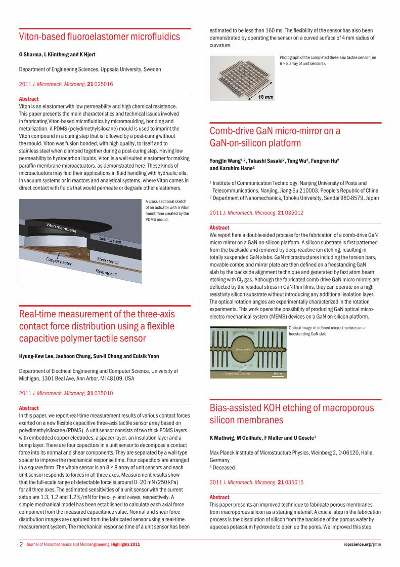
Viton-based fluoroelastomer microfluidics
G Sharma L Klintberg and K Hjort Department of Engineering Sciences Uppsala University Sweden
2011 J Micromech Microeng 21 025016 AbstractViton is an elastomer with low permeability and high chemical resistance This paper presents the main characteristics and technical issues involved in fabricating Viton-based microfluidics by micromoulding bonding and metallization A PDMS (polydimethylsiloxane) mould is used to imprint the Viton compound in a curing step that is followed by a post-curing without the mould Viton was fusion bonded with high quality to itself and to stainless steel when clamped together during a post-curing step Having low permeability to hydrocarbon liquids Viton is a well-suited elastomer for making paraffin membrane microactuators as demonstrated here These kinds of microactuators may find their applications in fluid handling with hydraulic oils in vacuum systems or in reactors and analytical systems where Viton comes in direct contact with fluids that would permeate or degrade other elastomers
Bias-assisted KOH etching of macroporous silicon membranes
K Mathwig M Geilhufe F Muumlller and U Goumlsele1
Max Planck Institute of Microstructure Physics Weinberg 2 D-06120 Halle Germany 1 Deceased
2011 J Micromech Microeng 21 035015 AbstractThis paper presents an improved technique to fabricate porous membranes from macroporous silicon as a starting material A crucial step in the fabrication process is the dissolution of silicon from the backside of the porous wafer by aqueous potassium hydroxide to open up the pores We improved this step
Comb-drive GaN micro-mirror on a GaN-on-silicon platform
Yongjin Wang12 Takashi Sasaki2 Tong Wu2 Fangren Hu2 and Kazuhiro Hane2
1 Institute of Communication Technology Nanjing University of Posts and
Telecommunications Nanjing Jiang-Su 210003 Peoples Republic of China 2 Department of Nanomechanics Tohoku University Sendai 980-8579 Japan
2011 J Micromech Microeng 21 035012 AbstractWe report here a double-sided process for the fabrication of a comb-drive GaN micro-mirror on a GaN-on-silicon platform A silicon substrate is first patterned from the backside and removed by deep reactive ion etching resulting in totally suspended GaN slabs GaN microstructures including the torsion bars movable combs and mirror plate are then defined on a freestanding GaN slab by the backside alignment technique and generated by fast atom beam etching with Cl2 gas Although the fabricated comb-drive GaN micro-mirrors are deflected by the residual stress in GaN thin films they can operate on a high resistivity silicon substrate without introducing any additional isolation layer The optical rotation angles are experimentally characterized in the rotation experiments This work opens the possibility of producing GaN optical micro-electro-mechanical-system (MEMS) devices on a GaN-on-silicon platformReal-time measurement of the three-axis
contact force distribution using a flexible capacitive polymer tactile sensor
Hyung-Kew Lee Jaehoon Chung Sun-Il Chang and Euisik Yoon Department of Electrical Engineering and Computer Science University of Michigan 1301 Beal Ave Ann Arbor MI 48109 USA
2011 J Micromech Microeng 21 035010 AbstractIn this paper we report real-time measurement results of various contact forces exerted on a new flexible capacitive three-axis tactile sensor array based on polydimethylsiloxane (PDMS) A unit sensor consists of two thick PDMS layers with embedded copper electrodes a spacer layer an insulation layer and a bump layer There are four capacitors in a unit sensor to decompose a contact force into its normal and shear components They are separated by a wall-type spacer to improve the mechanical response time Four capacitors are arranged in a square form The whole sensor is an 8 times 8 array of unit sensors and each unit sensor responds to forces in all three axes Measurement results show that the full-scale range of detectable force is around 0ndash20 mN (250 kPa) for all three axes The estimated sensitivities of a unit sensor with the current setup are 13 12 and 12mN for the x- y- and z-axes respectively A simple mechanical model has been established to calculate each axial force component from the measured capacitance value Normal and shear force distribution images are captured from the fabricated sensor using a real-time measurement system The mechanical response time of a unit sensor has been
A cross-sectional sketch of an actuator with a Viton membrane created by the PDMS mould
Optical image of defined microstructures on a freestanding GaN slab
Photograph of the completed three-axis tactile sensor (an 8 times 8 array of unit sensors)
estimated to be less than 160 ms The flexibility of the sensor has also been demonstrated by operating the sensor on a curved surface of 4 mm radius of curvature
iopscienceorgjmm Journal of Micromechanics and Microengineering Highlights 2011 3
Analysis of nanoscale mechanical grasping under ambient conditions
Hui Xie1 Pierre Lambert2 and Steacutephane Reacutegnier1
1 Institut des Systegravemes Intelligents et Robotique Universiteacute Pierre et Marie
CurieCNRS UMR7222 BC 173 4 Place Jussieu 75005 Paris France 2 BEAMS Department Universiteacute libre de Bruxelles CP 16556 50 Avenue FD
Roosevelt B-1050 Bruxelles Belgium
2011 J Micromech Microeng 21 045009 AbstractIn this paper in order to understand mechanical grasping at the nanoscale contact mechanics between nanogrippers and nanoobjects is studied Contact models are introduced to simulate elastic contacts between various profiles of a flat surface sphere and cylinder for different types of nanoobjects and nanogrippers Analyses and evaluation instances indicate that friction forces commonly used in macro-grasping to overcome gravity at the nanoscale are often insufficient to overcome the relatively strong adhesion forces when picking up the nanoobject deposited on a substrate due to the tiny contact area For stable nanoscale grasping nonparallel two-finger grippers with a lsquoVrsquo configuration are demonstrated to have better grasping capabilities than parallel grippers To achieve mechanical nanoscale grasping a nanogripper constructed from two microcantilevers is presented Experimental results for the pick-and-place manipulation of silicon nanowires validate the theoretical analyses and capabilities of the proposed nanogripper
Thermal nanoimprint process for high-temperature fabrication of mesoscale epitaxial exchange-biased metallic wire arrays
W Zhang1 D N Weiss23 and K M Krishnan1
1 Department of Materials Science and Engineering University of Washington
Seattle WA 98195 USA 2 Washington Technology Center Seattle WA 98195 USA 3 Department of Electrical Engineering University of Washington Seattle WA
98195 USA
2011 J Micromech Microeng 21 045024
Nonparallel configuration of the dual-tip nanogripper
by biasing the silicon wafer electrically against the KOH By monitoring the currentndashtime characteristics a good control of the process is achieved and the yield is improved Also the etching can be stopped instantaneously and automatically by short-circuiting Si and KOH Moreover the bias-assisted etching allows for the controlled fabrication of silicon dioxide tube arrays when the silicon pore walls are oxidized and inverted pores are released
A trans-scaled nanofabrication using 3D diffuser lithography metal molding and nano-imprinting
Dong-Haan Kim1 Joo-Hyung Lee Hyung Suk Lee2 and Jun-Bo Yoon Department of Electrical Engineering KAIST 335 Gwahangno Yuseong-gu Daejeon 305-701 Korea 1 Present address Doosan Heavy Industries and Construction Co Ltd
1303-22 Seocho-dong Seocho-gu Seoul 137-920 Korea 2 Present address Samsung Electronics Co Ltd San 16 Banwol-dong
Hwasung Gyeonggi-do 445ndash701 Korea
2011 J Micromech Microeng 21 045025 AbstractThis paper describes our proposal and successful demonstration of a trans-scaled nanofabrication using conventional micro-technologies In order to achieve this we first performed lsquo3D diffuser lithographyrsquo which is simply conventional contact microlithography with an optical diffuser sheet to make submicron-sized nanopatterns on a photoresist mold We then replicated these patterns onto a nickel mold thereby successfully fabricating nickel nano-tip arrays 300 nm in diameter without the use of any specially-designed nanopatterning equipment or techniques Then the conventional thermal nano-imprinting onto a PMMA target was conducted using the fabricated Ni stamp producing nano-dot arrays in an area of several hundreds of microns per side where each dot diameter was 700 nm with 58 uniformity The largest size which can accommodate this method depends on the size of the conventional contact lithography tool which currently extends to several meters according to contemporary machinery The proposed method is cost effective for mass production and can be applied to various fields of nanoscale applications
SEM images of the fabricated nano-tip arrays in the photoresist mold using 3D diffuser lithography
AbstractA thermal nanoimprint process for the high-temperature (400 degC) fabrication of submicron epitaxial metallic wire arrays over areas gt 1 times 1 cm2 is reported Based on a method using an imprinted polymeric bilayer resist template that is transferred to a metallic (molybdenum) mask this process is enabled by an appropriate undercut profile of the Mo mask The undercut profile is obtained from a distinctive wedge-shaped profile of the polymeric resist layers by carefully controlling the etch parameters Using flexible ethylene tetrafluoroethylene imprint molds we demonstrate defect-free imprinting on MgO substrates Epitaxial patterning is demonstrated with FeMnPd bilayer wire arrays subsequently grown along well-defined crystallographic orientations X-ray diffraction of the patterned arrays reveals that the MnPd can be grown in two different crystallographic orientations (c-axis and a-axis normals) The epitaxial nature of the patterned arrays is further confirmed by magnetic measurements that demonstrate the competing effects of intrinsic (magnetocrystalline and exchange) and lithography-induced shape anisotropies on the magnetization reversal characteristics along different directions with respect to the axis of the wire arrays
4 Journal of Micromechanics and Microengineering Highlights 2011 iopscienceorgjmm
Micromachined array-type Mirau interferometer for parallel inspection of MEMS
J Albero1 S Bargiel1 N Passilly1 P Dannberg2 M Stumpf2 U D Zeitner2 C Rousselot1 K Gastinger3 and C Gorecki1
1 Deacutepartement MN2S FEMTO-ST (UMR CNRS 6174) 16 Route de Gray 25030
Besanccedilon Cedex France 2 Fraunhofer IOF A-Einstein-Str 7 07745-Jena Germany 3 SINTEF IKT Optical Measurement Systems and Data Analysis N-7465
Trondheim Norway
2011 J Micromech Microeng 21 065005 AbstractWe present the development of an array type of micromachined Mirau interferometers operating in the regime of low coherence interferometry (LCI) and adapted for massively parallel inspection of MEMS The system is a combination of free-space micro-optical technologies and silicon micromachining based on the vertical assembly of two glass wafers The probing wafer carries an array of refractive microlenses diffractive gratings to correct chromatic and spherical aberrations and reference micro-mirrors The semitransparent beam splitter plate is based on the deposition of a dielectric multilayer sandwiched between two glass wafers The interferometer matrix is the key element of a novel inspection system aimed to perform parallel inspection of MEMS The fabricated demonstrator including 5 times 5 channels allows consequently decreasing the measurement time by a factor of 25 In the following the details of fabrication processes of the micro-optical components and their assembly are described The feasibility of the LCI is demonstrated for the measurement of a wafer of MEMS sensors
Single-DNA-molecule trapping with silicon nanotweezers using pulsed dielectrophoresis
Momoko Kumemura1 Dominique Collard12 Naoyoshi Sakaki1 Christophe Yamahata14 Maho Hosogi3 Gen Hashiguchi3 and Hiroyuki Fujita1
1 Institute of Industrial Science The University of Tokyo 4-6-1 Komaba
Meguro-ku Tokyo 153-8505 Japan 2 LIMMSCNRS-IIS (UMI 2820) The University of Tokyo 4-6-1 Komaba
Meguro-ku Tokyo 153-8505 Japan 3 Research Institute of Electronics Shizuoka University 3-5-1 Jyouhoku
Naka-ku Hamamatsu-shi Shizuoka 432-8011 Japan 4 Present address Ecole Polytechnique Feacutedeacuterale de Lausanne Microsystem
Lab CH-1015 Lausanne Switzerland
2011 J Micromech Microeng 21 054020
Fabrication and electrical integration of robust carbon nanotube micropillars by self-directed elastocapillary densification
Michaeumll F L De Volder123 Sei Jin Park1 Sameh H Tawfick1 Daniel O Vidaud1 and A John Hart1
1 Department of Mechanical Engineering University of Michigan 2350
Hayward Street Ann Arbor MI 48109 USA 2 IMEC Kapeldreef 75 3001 Heverlee Belgium 3 Department of Mechanical Engineering Katholieke Universiteit Leuven 3001
Leuven Belgium
2011 J Micromech Microeng 21 045033 AbstractVertically aligned carbon nanotube (CNT) lsquoforestrsquo microstructures fabricated by chemical vapor deposition (CVD) using patterned catalyst films typically have a low CNT density per unit area As a result CNT forests have poor bulk properties and are too fragile for integration with microfabrication processing We introduce a new self-directed capillary densification method where a liquid is controllably condensed onto and evaporated from the CNT forests Compared to prior approaches where the substrate with CNTs is immersed in a liquid our condensation approach gives significantly more uniform structures and enables precise control of the CNT packing density We present a set of design rules and parametric studies of CNT micropillar densification by self-directed capillary action and show that self-directed capillary densification enhances Youngs modulus and electrical conductivity of CNT micropillars by more than three orders of magnitude Owing to the outstanding properties of CNTs this scalable process will be useful for the integration of CNTs as a functional material in microfabricated devices for mechanical electrical thermal and biomedical applications
Effect of the catalyst pattern shape and the top crust on the pillar cross-section after densification (a) polygonal pillars (b) polygonal pillars where the crust was removed by plasma etching before densification
Optical image of the IR sensor formed through the probing wafer image produced by the lenses with the diffractive correction and the micromirror before the beam-splitter assembly
AbstractDNA manipulation based on dielectrophoresis between microfabricated electrodes is one of the most efficient methods for the physical handling of molecules Dielectrophoresis is routinely used for stretching and trapping DNA molecules between the opposing tips of silicon nanotweezers However the precise number of trapped molecules is difficult to predict as a continuous application of ac voltage continually attracts the molecules while the electric-field-induced fluid flow prevents them from bridging the tips To circumvent this difficulty the dielectrophoresis signal is applied during very short intervals In this pulsed mode the electrohydrodynamic fluid flow is lessened and the molecule trapping success rate is greatly enhanced A fluorescently labeled single λ-DNA molecule was successfully stretched and captured by the silicon nanotweezers with 50 ms pulses of a 1 MHz 1 MV mminus1 ac dielectrophoresis voltage This single-molecule trapping between the tweezers tips is monitored in real time under fluorescence imaging
iopscienceorgjmm Journal of Micromechanics and Microengineering Highlights 2011 5
Simulating anisotropic etching of silicon in any etchant evolutionary algorithm for the calibration of the continuous cellular automaton
M A Gosaacutelvez12 N Ferrando3 Y Xing4 Prem Pal5 K Sato1 J Cerdaacute3 and R Gadea3
1 Department of Micro-Nanosystems Engineering Nagoya University 464-
8603 Aichi Japan 2 Department of Materials Physics University of the Basque Country (UPV-
EHU) Donostia International Physics Center (DIPC) and Centro de Fiacutesica de Materiales (CFM-MPE) 20018 Donostia-San Sebastian Spain
3 Instituto de Intrumentacioacuten para Imagen Molecular Universidad Politeacutecnica de Valencia 46022 Valencia Spain
4 Laboratory for Micro-Nano Medical Devices Southeast University Nanjing Peoplersquos Republic of China
5 MEMS and MicroNano Systems Laboratory Department of Physics Indian Institute of Technology Hyderabad India
2011 J Micromech Microeng 21 065017 AbstractAn evolutionary algorithm is presented for the automated calibration of the continuous cellular automaton for the simulation of isotropic and anisotropic wet chemical etching of silicon in as many as 31 widely different and technologically relevant etchants including KOH KOH+IPA TMAH and TMAH+Triton in various concentrations and temperatures Based on state-of-the-art evolutionary operators we implement a robust algorithm for the simultaneous optimization of roughly 150 microscopic removal rates based on the minimization of a cost function with four quantitative error measures including (i) the error between simulated and experimental macroscopic etch rates for numerous surface orientations all over the unit sphere (ii) the error due to underetching asymmetries and floor corrugation features observed in simulated silicon samples masked using a circular pattern (iii) the error associated with departures from a step-flow-based hierarchy in the values of the microscopic removal rates and (iv) the error associated with deviations from a step-flow-based clustering of the microscopic removal rates For the first time we present the calibration and successful simulation of two technologically relevant CMOS compatible etchants namely TMAH and especially TMAH+Triton providing several comparisons between simulated and experimental MEMS structures based on multi-step etching in these etchants
Comparison of simulation and experiment for single-step etching Experiment (a)ndash(b) TMAH 25 wt + Triton 01 vol and (c) TMAH 25 wt Simulation (d)ndash(e) TMAH 25 wt + Triton 01 vol and (f ) TMAH 25 wt Mask patterns black = oxide white = bare silicon (T = 80 degC) The difference between R100 in (a)ndash(c) and Rtarget in (d)ndash(f ) is due to the fact that the EA calibrations have been obtained for slightly different etch rates than in (a)ndash(c) due to the variability of the experimental etch rates when different experiments are performed
Microfabrication of diamond-based slow-wave circuits for mm-wave and THz vacuum electronic sources
M R Lueck1 D M Malta1 K H Gilchrist1 C L Kory2 G T Mearini2
and J A Dayton2
1 Center for Materials and Electronic Technologies RTI International 3040
Cornwallis Road Research Triangle Park NC 27709 USA 2 Teraphysics 110 Alpha Park Cleveland OH USA
2011 J Micromech Microeng 21 065022 AbstractPlanar and helical slow-wave circuits for THz radiation sources have been made using novel microfabrication and assembly methods A biplanar slow-wave circuit for a 650 GHz backward wave oscillator (BWO) was fabricated through the growth of diamond into high aspect ratio silicon molds and the selective metallization of the tops and sidewalls of 90 μm tall diamond features using lithographically created shadow masks Helical slow-wave circuits for a 650 GHz BWO and a 95 GHz traveling wave tube were created through the patterning of trenches in thin film diamond electroplating of gold half-helices and high accuracy bonding of helix halves The development of new techniques for the microfabrication of vacuum electronic components will help to facilitate compact and high-power sources for terahertz range radiation
Formation of micronano-scale wrinkling patterns atop shape memory polymers
Y Zhao1 W M Huang1 and Y Q Fu2
1 School of Mechanical and Aerospace Engineering Nanyang Technological
University 50 Nanyang Avenue Singapore 639798 2 Thin Film Centre Scottish Union of Physics Alliance (SUPA) University of the
West of Scotland Paisley PA1 2BE UK
2011 J Micromech Microeng 21 067007 AbstractWrinkling patterns in shape memory polymer (SMP) sputter deposited with a thin layer (10 s nm in thickness) of gold atop are systematically investigated under various conditions Depending on the surface condition heating temperature and pre-straining different patterns of micronano-scaled wrinkles are produced Although elastic buckling of the gold layer is the mechanism behind all types of wrinkles the shape memory effect (SME) and thermal expansion mismatch (TEM) are the driving force for different patterns after heating to different temperatures ie the evolution of wrinkle pattern is due to the SME after heating to low temperatures and the TEM after heating to high temperatures The flexibility and convenience in using SMP to achieve different wrinkling patterns is demonstrated
SEM images of helical slow-wave circuits for (a b) the 95 GHz TWT and (c d) the 650 GHz BWO (b) The silicon has been partially etched away from the diamond for illustration The 95 GHz helix was fabricated with a rounded shape while the 650 GHz helix is square
(a)
(b)
6 Journal of Micromechanics and Microengineering Highlights 2011 iopscienceorgjmm
Low temperature wafer-level bonding for hermetic packaging of 3D microsystems
C S Tan14 J Fan124 D F Lim2 G Y Chong2 and K H Li3
1 CINTRA CNRSNTUTHALES UMI 3288 Research Techno Plaza 50 Nanyang
Drive Singapore 637553 2 School of Electrical and Electronic Engineering Nanyang Technological
University 50 Nanyang Avenue Singapore 639798 3 Temasek LaboratoriesNTU Nanyang Technological University Research
Techno Plaza 50 Nanyang Drive Singapore 637553 4 Contributed equally to this work
2011 J Micromech Microeng 21 075006 AbstractMetallic copperndashcopper (CundashCu) thermo-compression bonding oxidendashoxide (SiO2ndashSiO2) fusion bonding and siliconndashsilicon (SindashSi) direct bonding are investigated for potential application as hermetic seal in 3D microsystem packaging Cavities are etched to a volume of 14 times 10minus3 cm3 in accordance with the MIL-STD-883E standard prescribed for microelectronics packaging In the case of metal bonding a clean Cu layer with a thickness of 300 nm and a Ti barrier layer with an underlying thickness of 50 nm are used The wafer pair is bonded at 300 degC under the application of a bonding force of 5500 N for 1 h On the other hand SindashSi bonding and SiO2ndashSiO2 bonding are initiated at room ambient after surface activation followed by annealing in inert ambient at 300 degC for 1 h The bonded cavities are stored in a helium bomb chamber and the leak rate is measured with a mass spectrometer An excellent helium leak rate below 5 times 10minus9 atm cm3 sminus1 is detected for all cases and this is at least ten times better than the reject limit
A self-adaptive thermal switch array for rapid temperature stabilization under various thermal power inputs
Xiaobao Geng Pragnesh Patel Amitabh Narain and Dennis Desheng Meng Multi-Scale Energy System (MuSES) Laboratory Department of Mechanical Engineering Engineering Mechanics Michigan Technological University 815 R L Smith Building 1400 Townsend Drive Houghton MI 49931 USA
2011 J Micromech Microeng 21 085018 AbstractA self-adaptive thermal switch array (TSA) based on actuation by low-melting-point alloy droplets is reported to stabilize the temperature of a heat-generating microelectromechanical system (MEMS) device at a predetermined range (ie the optimal working temperature of the device) with neither a control circuit nor electrical power consumption When the temperature is below this range the TSA stays off and works as a thermal insulator Therefore the MEMS device can quickly heat itself up to its optimal working temperature during startup Once this temperature is reached TSA is automatically turned on to increase the thermal conductance working as an effective thermal spreader As a result the MEMS device tends to stay at its optimal working temperature without complex thermal management components and the associated parasitic power loss A prototype TSA was fabricated and characterized to prove the concept The stabilization temperatures under various power inputs have been studied both experimentally and theoretically Under the increment of power input from 38 to 58 W the temperature of the device increased only by 25 degC due to the stabilization effect of TSA
50 nm thick AlN film-based piezoelectric cantilevers for gravimetric detection
P Ivaldi1 J Abergel1 M H Matheny2 L G Villanueva2 R B Karabalin2 M L Roukes2 P Andreucci1 S Hentz12 and E Defayuml1
1 CEA-LETI MINATEC Campus 17 Rue des Martyrs 38054 Grenoble Cedex 9 France 2 Kavli Nanoscience Institute California Institute of Technology Pasadena CA
91125 USA
2011 J Micromech Microeng 21 085023 AbstractDue to low power operation intrinsic integrability and compatibility with CMOS processing aluminum nitride (AlN) piezoelectric (PZE) microcantilevers are a very attractive paradigm for resonant gas sensing In this paper we theoretically investigate their ultimate limit of detection and enunciate design rules for performance optimization The reduction of the AlN layer thickness is found to be critical We further report the successful development and implementation in cantilever structures with a 50 nm thick active PZE AlN layer Material characterizations demonstrate that the PZE e31 coefficient can remain as high as 08 C mminus2 Electrically transduced frequency responses of the fabricated devices are in good agreement with analytical predictions Finally we demonstrate the excellent frequency stability with a 10minus8 minimum Allan deviation This exceptionally low noise operation allows us to expect a limit of detection as low as 53 zg μmminus2 and demonstrate the strong potential of AlN PZE microcantilevers for high resolution gas detection
Room temperature direct bonding of LiNbO3 crystal layers and its application to high-voltage optical sensing
D Tulli1 D Janner1 and V Pruneri12
1 ICFOmdashInstitut de Ciegravencies Fotograveniques Mediterranean Technology Park
08860 Castelldefels Barcelona Spain 2 ICREAmdashInstitucioacute Catalana de Recerca i Estudis Avanccedilats Barcelona Spain
2011 J Micromech Microeng 21 085025
SEM picture of the fabricated cantilever
Working principle of a self-adaptive TSA (a) TSA stays off under low temperature (b) LMA droplets melt to automatically turn the TSA on under high temperature
iopscienceorgjmm Journal of Micromechanics and Microengineering Highlights 2011 7
Analytical extraction of residual stresses and gradients in MEMS structures with application to CMOS-layered materials
F Fachin1 S A Nikles2 J Dugundji1 and B L Wardle1
1 Massachusetts Institute of Technology 77 Massachusetts Avenue
Cambridge MA 02139 USA 2 MEMSIC Inc Andover MA 01810 USA
2011 J Micromech Microeng 21 095017 AbstractAccurate thin-film characterization is a key requirement in the MEMS industry Residual stresses determine both the final shape and the functionality of released micromachined structures and should therefore be accurately assessed To date a number of techniques to characterize thin-film materials have been developed from substrate curvature measurement to methods that exploit the post-release deformation of test structures These techniques have some major drawbacks from high implementation costs to accuracy limitations due to improper boundary condition modeling Here we present a new technique for the characterization of multilayered composite MEMS structures that uses easily accessible experimental information on the post-release deformation of microbridges only with no need for multiple beam lengths The method is based on an analytical solution of the (post-)buckling problem of microbridges including the effect of residual stresses (both mean and gradient) and non-ideal clamping (boundary flexibility) The method allows simultaneous characterization of both the mean and the gradient residual stress components as well as the effective boundary condition associated with the fabrication process yielding approximately one order of magnitude improvement in resolution compared to extant methods using the same type and number of test structures The higher resolution is largely attributable to proper accounting for boundary flexibility by our method with the boundary condition for the structures in this work being ~90 as stiff in bending relative to the commonly assumed perfectly clamped condition Additional enhancement can be achieved with post-release deformation measurements of simple cantilevers in addition to the microbridges The method is useful as it ensures very low stress extraction uncertainty using a limited number of microbridge test structures and it is transferrable to package-stress characterization The analytical approach can also be extended to device design quantifying the effect of residual stresses and boundary flexibility on a structurersquos post-release state
A smart and self-sufficient frequency tunable vibration energy harvester
C Eichhorn R Tchagsim N Wilhelm and P Woias Department of Microsystems Engineering (IMTEK) University of Freiburg Freiburg Germany
2011 J Micromech Microeng 21 104003 AbstractWe present a piezoelectric energy-harvesting system which is able to self-tune its resonance frequency in an energy-autonomous way in order to extend its efficient operation over a large frequency range The system consists of a resonant and frequency-tunable piezoelectric generator and a control unit In predefined temporal intervals the control unit analyzes the ambient vibration frequency decides whether an adjustment of the generators resonance frequency is necessary or not and delivers the appropriate voltage to a piezoelectric actuator which alters the generatorrsquos mechanical stiffness to tune its resonance frequency The control unit has been optimized to an ultralow power consumption which means that up to 90 of the harvested energy can be fed to the powered electrical load which could be an embedded system With frequency-tunable generators the application range of vibration energy harvesters can be extended to environments with a non-constant vibration frequency like eg the surface of an engine with a varying number of revolutions per minute Furthermore the presented system opens the door to off-the-shelf solutions for environments with constant but uncommon vibration frequencies With the smart tuning algorithm presented in this work our system is even able to compensate typical weak points of piezoelectrically tunable harvesters like eg hysteresis effects the temperature dependence of the mechanical stiffness and aging effects
AbstractLiNbO3 is a crystal widely used in photonics and acoustics for example in electro-optic modulation nonlinear optical frequency conversion electric field sensing and surface acoustic wave filtering It often needs to be combined with other materials and used in thin layers to achieve the adequate device performance In this paper we investigate direct bonding of LiNbO3 crystals with other dielectric materials such as Si and fused silica (SiO2) and we show that specific surface chemical cleaning together with Ar or O2 plasma activation can be used to increase the surface free energy and achieve effective bonding at room temperature The resulting hybrid material bonding is very strong making the dicing and grinding of LiNbO3 layers as thin as 15 μm possible To demonstrate the application potentials of the proposed bonding technique we have fabricated and characterized a high-voltage field sensor with high sensitivity in a domain inverted and bonded LiNbO3 waveguide substrate
Effects of acoustic vibration on microheater-induced vapor bubble incipience in a microchannel
Xiaopeng Qu and Huihe Qiu Department of Mechanical Engineering Hong Kong University of Science and Technology Clear Water Bay Kowloon Hong Kong
2011 J Micromech Microeng 21 105015 AbstractA simultaneous temperature measurement and high-speed visualization study has been carried out to investigate the effects of acoustic vibration on vapor bubble dynamics and flow boiling in a single microchannel which is formed by bonding a bottom Pyrex glass wall with a top PDMS (polydimethylsiloxane) wall A single platinum serpentine microheater fabricated on the Pyrex glass substrate and integrated into the microchannel is used to generate vapor bubbles and measure local wall temperature simultaneously The temperature variations and flow pattern maps in terms of acoustic frequency and acoustic signal amplitude are presented respectively It is found that the acoustic vibration can induce bubble incipience with a relatively low heating power The frequency acoustic signal amplitude and flow rate are important factors affecting vapor bubble incipience A lower acoustic signal amplitude can promote bubble incipience to happen easily but no obvious effect when further increasing the acoustic amplitude to a relatively high level A low flow rate can advance bubble incipience while a very high flow rate can hinder bubble incipience under the same acoustic and heating conditions The experimental results are instructive for the design of novel microfluid and MEMS (microelectromechanical systems) devices such as lab-on-a-chip or thermal management devices
FE-SEM micrograph of a gold nano-dot array generated by annealing
8 Journal of Micromechanics and Microengineering Highlights 2011 iopscienceorgjmm
Rapid fabrication of an ordered nano-dot array by the combination of nano-plastic forming and annealing methods
Masahiko Yoshino Hiroki Ohsawa and Akinori Yamanaka Tokyo Institute of Technology 2-12-1 O-okayama Meguroku Tokyo 152-8552 Japan
2011 J Micromech Microeng 21 125017 AbstractIn this paper a new fabrication method for an ordered nano-dot array is developed Combination of coating nano-plastic forming and annealing processes is studied to produce uniformly sized and ordered gold nano-dot array on a quartz glass substrate The experimental results reveal that patterning of a groove grid on the gold-coated substrate with NPF is effective to obtain the ordered gold nano-dot array In the proposed fabrication process the size of the gold nano-dot can be controlled by adjusting the groove grid size A minimum gold nano-dot array fabricated on a quartz-glass substrate was 93 nm in diameter and 100 nm in pitch Furthermore the mechanism of nano-dot array generation by the presented process is investigated Using a theoretical model it is revealed that the proposed method is capable of fabrication of smaller nano-dots than 10 nm by controlling process conditions adequately
Integrated nanohole array surface plasmon resonance sensing device using a dual-wavelength source
C Escobedo1 S Vincent2 A I K Choudhury2 J Campbell2 A G Brolo3 D Sinton4 and R Gordon2
1 Department of Mechanical Engineering University of Victoria PO Box 3055
STN CSC V8W 3P6 Victoria BC Canada 2 Department of Electrical and Computer Engineering University of Victoria
PO Box 3055 V8W 3P6 Victoria BC Canada 3 Department of Chemistry University of Victoria V8P 5C2 Victoria BC
Canada 4 Department of Mechanical and Industrial Engineering University of Toronto
5 Kings College Rd M5S 3G8 Toronto ON Canada
2011 J Micromech Microeng 21 115001 AbstractIn this paper we demonstrate a compact integrated nanohole array-based surface plasmon resonance sensing device The unit includes a LED light source driving circuitry CCD detector microfluidic network and computer interface all assembled from readily available commercial components A dual-wavelength LED scheme was implemented to increase spectral diversity and isolate intensity variations to be expected in the field The prototype shows bulk sensitivity of 266 pixel intensity unitsRIU and a limit of detection of 6 times 10minus4 RIU Surface binding tests were performed demonstrating functionality as a surface-based sensing system This work is particularly relevant for low-cost point-of-care applications especially those involving multiple tests and field studies While nanohole arrays have been applied to many sensing applications and their suitability to device integration is well established this is the first demonstration of a fully integrated nanohole array-based sensing device
The effect of meniscus on the permeability of micro-post arrays
Chan Byon and Sung Jin Kim School of Mechanical Aerospace and Systems Engineering Korea Advanced Institute of Science and Technology Daejeon 305-701 Korea
2011 J Micromech Microeng 21 115011 AbstractThis study aims to investigate the effect of meniscus curvature on the permeability of the micro-post arrays which are widely used for applications of microfluidics An analytical model that accounts for the meniscus curvature
Biotinndashstreptavidin binding curve for the array of 275 nm hole size and 420 nm hole pitch The streptavidin solution was introduced at 10 min And saturation was achieved after sim40 min
SEM image of the copper micro-post-array fabricated in this study post-array (hexagonal d = 60 μm l = 90 μm H = 90 μm)
is developed The model considers two common array types quadratic and hexagonal arrays The permeability of micro-post arrays is estimated using the capillary rate of rise experiment and numerical simulation The results obtained from the analytical model match the experimental and numerical results within the error of 5 over the range of parameters commonly found in microfluidic applications (006 lt d lt 06 and H gt 02) where d and H are the post-diameter and the post-height respectively which are normalized by the pitch Based on the analytic results the effects of the post-diameter post-height and the contact angle on the permeability of post-arrays are investigated It is shown that the previous permeability models based on the flat meniscus assumption overestimate the experimental value by 26 for the quadratic array and 24 for the hexagonal array when cos θ = 1 d = 05 and H =1 The effect of the meniscus curvature is shown to become more pronounced as the contact angle or the post-height decreases
2 Journal of Micromechanics and Microengineering Highlights 2011 iopscienceorgjmm
Viton-based fluoroelastomer microfluidics
G Sharma L Klintberg and K Hjort Department of Engineering Sciences Uppsala University Sweden
2011 J Micromech Microeng 21 025016 AbstractViton is an elastomer with low permeability and high chemical resistance This paper presents the main characteristics and technical issues involved in fabricating Viton-based microfluidics by micromoulding bonding and metallization A PDMS (polydimethylsiloxane) mould is used to imprint the Viton compound in a curing step that is followed by a post-curing without the mould Viton was fusion bonded with high quality to itself and to stainless steel when clamped together during a post-curing step Having low permeability to hydrocarbon liquids Viton is a well-suited elastomer for making paraffin membrane microactuators as demonstrated here These kinds of microactuators may find their applications in fluid handling with hydraulic oils in vacuum systems or in reactors and analytical systems where Viton comes in direct contact with fluids that would permeate or degrade other elastomers
Bias-assisted KOH etching of macroporous silicon membranes
K Mathwig M Geilhufe F Muumlller and U Goumlsele1
Max Planck Institute of Microstructure Physics Weinberg 2 D-06120 Halle Germany 1 Deceased
2011 J Micromech Microeng 21 035015 AbstractThis paper presents an improved technique to fabricate porous membranes from macroporous silicon as a starting material A crucial step in the fabrication process is the dissolution of silicon from the backside of the porous wafer by aqueous potassium hydroxide to open up the pores We improved this step
Comb-drive GaN micro-mirror on a GaN-on-silicon platform
Yongjin Wang12 Takashi Sasaki2 Tong Wu2 Fangren Hu2 and Kazuhiro Hane2
1 Institute of Communication Technology Nanjing University of Posts and
Telecommunications Nanjing Jiang-Su 210003 Peoples Republic of China 2 Department of Nanomechanics Tohoku University Sendai 980-8579 Japan
2011 J Micromech Microeng 21 035012 AbstractWe report here a double-sided process for the fabrication of a comb-drive GaN micro-mirror on a GaN-on-silicon platform A silicon substrate is first patterned from the backside and removed by deep reactive ion etching resulting in totally suspended GaN slabs GaN microstructures including the torsion bars movable combs and mirror plate are then defined on a freestanding GaN slab by the backside alignment technique and generated by fast atom beam etching with Cl2 gas Although the fabricated comb-drive GaN micro-mirrors are deflected by the residual stress in GaN thin films they can operate on a high resistivity silicon substrate without introducing any additional isolation layer The optical rotation angles are experimentally characterized in the rotation experiments This work opens the possibility of producing GaN optical micro-electro-mechanical-system (MEMS) devices on a GaN-on-silicon platformReal-time measurement of the three-axis
contact force distribution using a flexible capacitive polymer tactile sensor
Hyung-Kew Lee Jaehoon Chung Sun-Il Chang and Euisik Yoon Department of Electrical Engineering and Computer Science University of Michigan 1301 Beal Ave Ann Arbor MI 48109 USA
2011 J Micromech Microeng 21 035010 AbstractIn this paper we report real-time measurement results of various contact forces exerted on a new flexible capacitive three-axis tactile sensor array based on polydimethylsiloxane (PDMS) A unit sensor consists of two thick PDMS layers with embedded copper electrodes a spacer layer an insulation layer and a bump layer There are four capacitors in a unit sensor to decompose a contact force into its normal and shear components They are separated by a wall-type spacer to improve the mechanical response time Four capacitors are arranged in a square form The whole sensor is an 8 times 8 array of unit sensors and each unit sensor responds to forces in all three axes Measurement results show that the full-scale range of detectable force is around 0ndash20 mN (250 kPa) for all three axes The estimated sensitivities of a unit sensor with the current setup are 13 12 and 12mN for the x- y- and z-axes respectively A simple mechanical model has been established to calculate each axial force component from the measured capacitance value Normal and shear force distribution images are captured from the fabricated sensor using a real-time measurement system The mechanical response time of a unit sensor has been
A cross-sectional sketch of an actuator with a Viton membrane created by the PDMS mould
Optical image of defined microstructures on a freestanding GaN slab
Photograph of the completed three-axis tactile sensor (an 8 times 8 array of unit sensors)
estimated to be less than 160 ms The flexibility of the sensor has also been demonstrated by operating the sensor on a curved surface of 4 mm radius of curvature
iopscienceorgjmm Journal of Micromechanics and Microengineering Highlights 2011 3
Analysis of nanoscale mechanical grasping under ambient conditions
Hui Xie1 Pierre Lambert2 and Steacutephane Reacutegnier1
1 Institut des Systegravemes Intelligents et Robotique Universiteacute Pierre et Marie
CurieCNRS UMR7222 BC 173 4 Place Jussieu 75005 Paris France 2 BEAMS Department Universiteacute libre de Bruxelles CP 16556 50 Avenue FD
Roosevelt B-1050 Bruxelles Belgium
2011 J Micromech Microeng 21 045009 AbstractIn this paper in order to understand mechanical grasping at the nanoscale contact mechanics between nanogrippers and nanoobjects is studied Contact models are introduced to simulate elastic contacts between various profiles of a flat surface sphere and cylinder for different types of nanoobjects and nanogrippers Analyses and evaluation instances indicate that friction forces commonly used in macro-grasping to overcome gravity at the nanoscale are often insufficient to overcome the relatively strong adhesion forces when picking up the nanoobject deposited on a substrate due to the tiny contact area For stable nanoscale grasping nonparallel two-finger grippers with a lsquoVrsquo configuration are demonstrated to have better grasping capabilities than parallel grippers To achieve mechanical nanoscale grasping a nanogripper constructed from two microcantilevers is presented Experimental results for the pick-and-place manipulation of silicon nanowires validate the theoretical analyses and capabilities of the proposed nanogripper
Thermal nanoimprint process for high-temperature fabrication of mesoscale epitaxial exchange-biased metallic wire arrays
W Zhang1 D N Weiss23 and K M Krishnan1
1 Department of Materials Science and Engineering University of Washington
Seattle WA 98195 USA 2 Washington Technology Center Seattle WA 98195 USA 3 Department of Electrical Engineering University of Washington Seattle WA
98195 USA
2011 J Micromech Microeng 21 045024
Nonparallel configuration of the dual-tip nanogripper
by biasing the silicon wafer electrically against the KOH By monitoring the currentndashtime characteristics a good control of the process is achieved and the yield is improved Also the etching can be stopped instantaneously and automatically by short-circuiting Si and KOH Moreover the bias-assisted etching allows for the controlled fabrication of silicon dioxide tube arrays when the silicon pore walls are oxidized and inverted pores are released
A trans-scaled nanofabrication using 3D diffuser lithography metal molding and nano-imprinting
Dong-Haan Kim1 Joo-Hyung Lee Hyung Suk Lee2 and Jun-Bo Yoon Department of Electrical Engineering KAIST 335 Gwahangno Yuseong-gu Daejeon 305-701 Korea 1 Present address Doosan Heavy Industries and Construction Co Ltd
1303-22 Seocho-dong Seocho-gu Seoul 137-920 Korea 2 Present address Samsung Electronics Co Ltd San 16 Banwol-dong
Hwasung Gyeonggi-do 445ndash701 Korea
2011 J Micromech Microeng 21 045025 AbstractThis paper describes our proposal and successful demonstration of a trans-scaled nanofabrication using conventional micro-technologies In order to achieve this we first performed lsquo3D diffuser lithographyrsquo which is simply conventional contact microlithography with an optical diffuser sheet to make submicron-sized nanopatterns on a photoresist mold We then replicated these patterns onto a nickel mold thereby successfully fabricating nickel nano-tip arrays 300 nm in diameter without the use of any specially-designed nanopatterning equipment or techniques Then the conventional thermal nano-imprinting onto a PMMA target was conducted using the fabricated Ni stamp producing nano-dot arrays in an area of several hundreds of microns per side where each dot diameter was 700 nm with 58 uniformity The largest size which can accommodate this method depends on the size of the conventional contact lithography tool which currently extends to several meters according to contemporary machinery The proposed method is cost effective for mass production and can be applied to various fields of nanoscale applications
SEM images of the fabricated nano-tip arrays in the photoresist mold using 3D diffuser lithography
AbstractA thermal nanoimprint process for the high-temperature (400 degC) fabrication of submicron epitaxial metallic wire arrays over areas gt 1 times 1 cm2 is reported Based on a method using an imprinted polymeric bilayer resist template that is transferred to a metallic (molybdenum) mask this process is enabled by an appropriate undercut profile of the Mo mask The undercut profile is obtained from a distinctive wedge-shaped profile of the polymeric resist layers by carefully controlling the etch parameters Using flexible ethylene tetrafluoroethylene imprint molds we demonstrate defect-free imprinting on MgO substrates Epitaxial patterning is demonstrated with FeMnPd bilayer wire arrays subsequently grown along well-defined crystallographic orientations X-ray diffraction of the patterned arrays reveals that the MnPd can be grown in two different crystallographic orientations (c-axis and a-axis normals) The epitaxial nature of the patterned arrays is further confirmed by magnetic measurements that demonstrate the competing effects of intrinsic (magnetocrystalline and exchange) and lithography-induced shape anisotropies on the magnetization reversal characteristics along different directions with respect to the axis of the wire arrays
4 Journal of Micromechanics and Microengineering Highlights 2011 iopscienceorgjmm
Micromachined array-type Mirau interferometer for parallel inspection of MEMS
J Albero1 S Bargiel1 N Passilly1 P Dannberg2 M Stumpf2 U D Zeitner2 C Rousselot1 K Gastinger3 and C Gorecki1
1 Deacutepartement MN2S FEMTO-ST (UMR CNRS 6174) 16 Route de Gray 25030
Besanccedilon Cedex France 2 Fraunhofer IOF A-Einstein-Str 7 07745-Jena Germany 3 SINTEF IKT Optical Measurement Systems and Data Analysis N-7465
Trondheim Norway
2011 J Micromech Microeng 21 065005 AbstractWe present the development of an array type of micromachined Mirau interferometers operating in the regime of low coherence interferometry (LCI) and adapted for massively parallel inspection of MEMS The system is a combination of free-space micro-optical technologies and silicon micromachining based on the vertical assembly of two glass wafers The probing wafer carries an array of refractive microlenses diffractive gratings to correct chromatic and spherical aberrations and reference micro-mirrors The semitransparent beam splitter plate is based on the deposition of a dielectric multilayer sandwiched between two glass wafers The interferometer matrix is the key element of a novel inspection system aimed to perform parallel inspection of MEMS The fabricated demonstrator including 5 times 5 channels allows consequently decreasing the measurement time by a factor of 25 In the following the details of fabrication processes of the micro-optical components and their assembly are described The feasibility of the LCI is demonstrated for the measurement of a wafer of MEMS sensors
Single-DNA-molecule trapping with silicon nanotweezers using pulsed dielectrophoresis
Momoko Kumemura1 Dominique Collard12 Naoyoshi Sakaki1 Christophe Yamahata14 Maho Hosogi3 Gen Hashiguchi3 and Hiroyuki Fujita1
1 Institute of Industrial Science The University of Tokyo 4-6-1 Komaba
Meguro-ku Tokyo 153-8505 Japan 2 LIMMSCNRS-IIS (UMI 2820) The University of Tokyo 4-6-1 Komaba
Meguro-ku Tokyo 153-8505 Japan 3 Research Institute of Electronics Shizuoka University 3-5-1 Jyouhoku
Naka-ku Hamamatsu-shi Shizuoka 432-8011 Japan 4 Present address Ecole Polytechnique Feacutedeacuterale de Lausanne Microsystem
Lab CH-1015 Lausanne Switzerland
2011 J Micromech Microeng 21 054020
Fabrication and electrical integration of robust carbon nanotube micropillars by self-directed elastocapillary densification
Michaeumll F L De Volder123 Sei Jin Park1 Sameh H Tawfick1 Daniel O Vidaud1 and A John Hart1
1 Department of Mechanical Engineering University of Michigan 2350
Hayward Street Ann Arbor MI 48109 USA 2 IMEC Kapeldreef 75 3001 Heverlee Belgium 3 Department of Mechanical Engineering Katholieke Universiteit Leuven 3001
Leuven Belgium
2011 J Micromech Microeng 21 045033 AbstractVertically aligned carbon nanotube (CNT) lsquoforestrsquo microstructures fabricated by chemical vapor deposition (CVD) using patterned catalyst films typically have a low CNT density per unit area As a result CNT forests have poor bulk properties and are too fragile for integration with microfabrication processing We introduce a new self-directed capillary densification method where a liquid is controllably condensed onto and evaporated from the CNT forests Compared to prior approaches where the substrate with CNTs is immersed in a liquid our condensation approach gives significantly more uniform structures and enables precise control of the CNT packing density We present a set of design rules and parametric studies of CNT micropillar densification by self-directed capillary action and show that self-directed capillary densification enhances Youngs modulus and electrical conductivity of CNT micropillars by more than three orders of magnitude Owing to the outstanding properties of CNTs this scalable process will be useful for the integration of CNTs as a functional material in microfabricated devices for mechanical electrical thermal and biomedical applications
Effect of the catalyst pattern shape and the top crust on the pillar cross-section after densification (a) polygonal pillars (b) polygonal pillars where the crust was removed by plasma etching before densification
Optical image of the IR sensor formed through the probing wafer image produced by the lenses with the diffractive correction and the micromirror before the beam-splitter assembly
AbstractDNA manipulation based on dielectrophoresis between microfabricated electrodes is one of the most efficient methods for the physical handling of molecules Dielectrophoresis is routinely used for stretching and trapping DNA molecules between the opposing tips of silicon nanotweezers However the precise number of trapped molecules is difficult to predict as a continuous application of ac voltage continually attracts the molecules while the electric-field-induced fluid flow prevents them from bridging the tips To circumvent this difficulty the dielectrophoresis signal is applied during very short intervals In this pulsed mode the electrohydrodynamic fluid flow is lessened and the molecule trapping success rate is greatly enhanced A fluorescently labeled single λ-DNA molecule was successfully stretched and captured by the silicon nanotweezers with 50 ms pulses of a 1 MHz 1 MV mminus1 ac dielectrophoresis voltage This single-molecule trapping between the tweezers tips is monitored in real time under fluorescence imaging
iopscienceorgjmm Journal of Micromechanics and Microengineering Highlights 2011 5
Simulating anisotropic etching of silicon in any etchant evolutionary algorithm for the calibration of the continuous cellular automaton
M A Gosaacutelvez12 N Ferrando3 Y Xing4 Prem Pal5 K Sato1 J Cerdaacute3 and R Gadea3
1 Department of Micro-Nanosystems Engineering Nagoya University 464-
8603 Aichi Japan 2 Department of Materials Physics University of the Basque Country (UPV-
EHU) Donostia International Physics Center (DIPC) and Centro de Fiacutesica de Materiales (CFM-MPE) 20018 Donostia-San Sebastian Spain
3 Instituto de Intrumentacioacuten para Imagen Molecular Universidad Politeacutecnica de Valencia 46022 Valencia Spain
4 Laboratory for Micro-Nano Medical Devices Southeast University Nanjing Peoplersquos Republic of China
5 MEMS and MicroNano Systems Laboratory Department of Physics Indian Institute of Technology Hyderabad India
2011 J Micromech Microeng 21 065017 AbstractAn evolutionary algorithm is presented for the automated calibration of the continuous cellular automaton for the simulation of isotropic and anisotropic wet chemical etching of silicon in as many as 31 widely different and technologically relevant etchants including KOH KOH+IPA TMAH and TMAH+Triton in various concentrations and temperatures Based on state-of-the-art evolutionary operators we implement a robust algorithm for the simultaneous optimization of roughly 150 microscopic removal rates based on the minimization of a cost function with four quantitative error measures including (i) the error between simulated and experimental macroscopic etch rates for numerous surface orientations all over the unit sphere (ii) the error due to underetching asymmetries and floor corrugation features observed in simulated silicon samples masked using a circular pattern (iii) the error associated with departures from a step-flow-based hierarchy in the values of the microscopic removal rates and (iv) the error associated with deviations from a step-flow-based clustering of the microscopic removal rates For the first time we present the calibration and successful simulation of two technologically relevant CMOS compatible etchants namely TMAH and especially TMAH+Triton providing several comparisons between simulated and experimental MEMS structures based on multi-step etching in these etchants
Comparison of simulation and experiment for single-step etching Experiment (a)ndash(b) TMAH 25 wt + Triton 01 vol and (c) TMAH 25 wt Simulation (d)ndash(e) TMAH 25 wt + Triton 01 vol and (f ) TMAH 25 wt Mask patterns black = oxide white = bare silicon (T = 80 degC) The difference between R100 in (a)ndash(c) and Rtarget in (d)ndash(f ) is due to the fact that the EA calibrations have been obtained for slightly different etch rates than in (a)ndash(c) due to the variability of the experimental etch rates when different experiments are performed
Microfabrication of diamond-based slow-wave circuits for mm-wave and THz vacuum electronic sources
M R Lueck1 D M Malta1 K H Gilchrist1 C L Kory2 G T Mearini2
and J A Dayton2
1 Center for Materials and Electronic Technologies RTI International 3040
Cornwallis Road Research Triangle Park NC 27709 USA 2 Teraphysics 110 Alpha Park Cleveland OH USA
2011 J Micromech Microeng 21 065022 AbstractPlanar and helical slow-wave circuits for THz radiation sources have been made using novel microfabrication and assembly methods A biplanar slow-wave circuit for a 650 GHz backward wave oscillator (BWO) was fabricated through the growth of diamond into high aspect ratio silicon molds and the selective metallization of the tops and sidewalls of 90 μm tall diamond features using lithographically created shadow masks Helical slow-wave circuits for a 650 GHz BWO and a 95 GHz traveling wave tube were created through the patterning of trenches in thin film diamond electroplating of gold half-helices and high accuracy bonding of helix halves The development of new techniques for the microfabrication of vacuum electronic components will help to facilitate compact and high-power sources for terahertz range radiation
Formation of micronano-scale wrinkling patterns atop shape memory polymers
Y Zhao1 W M Huang1 and Y Q Fu2
1 School of Mechanical and Aerospace Engineering Nanyang Technological
University 50 Nanyang Avenue Singapore 639798 2 Thin Film Centre Scottish Union of Physics Alliance (SUPA) University of the
West of Scotland Paisley PA1 2BE UK
2011 J Micromech Microeng 21 067007 AbstractWrinkling patterns in shape memory polymer (SMP) sputter deposited with a thin layer (10 s nm in thickness) of gold atop are systematically investigated under various conditions Depending on the surface condition heating temperature and pre-straining different patterns of micronano-scaled wrinkles are produced Although elastic buckling of the gold layer is the mechanism behind all types of wrinkles the shape memory effect (SME) and thermal expansion mismatch (TEM) are the driving force for different patterns after heating to different temperatures ie the evolution of wrinkle pattern is due to the SME after heating to low temperatures and the TEM after heating to high temperatures The flexibility and convenience in using SMP to achieve different wrinkling patterns is demonstrated
SEM images of helical slow-wave circuits for (a b) the 95 GHz TWT and (c d) the 650 GHz BWO (b) The silicon has been partially etched away from the diamond for illustration The 95 GHz helix was fabricated with a rounded shape while the 650 GHz helix is square
(a)
(b)
6 Journal of Micromechanics and Microengineering Highlights 2011 iopscienceorgjmm
Low temperature wafer-level bonding for hermetic packaging of 3D microsystems
C S Tan14 J Fan124 D F Lim2 G Y Chong2 and K H Li3
1 CINTRA CNRSNTUTHALES UMI 3288 Research Techno Plaza 50 Nanyang
Drive Singapore 637553 2 School of Electrical and Electronic Engineering Nanyang Technological
University 50 Nanyang Avenue Singapore 639798 3 Temasek LaboratoriesNTU Nanyang Technological University Research
Techno Plaza 50 Nanyang Drive Singapore 637553 4 Contributed equally to this work
2011 J Micromech Microeng 21 075006 AbstractMetallic copperndashcopper (CundashCu) thermo-compression bonding oxidendashoxide (SiO2ndashSiO2) fusion bonding and siliconndashsilicon (SindashSi) direct bonding are investigated for potential application as hermetic seal in 3D microsystem packaging Cavities are etched to a volume of 14 times 10minus3 cm3 in accordance with the MIL-STD-883E standard prescribed for microelectronics packaging In the case of metal bonding a clean Cu layer with a thickness of 300 nm and a Ti barrier layer with an underlying thickness of 50 nm are used The wafer pair is bonded at 300 degC under the application of a bonding force of 5500 N for 1 h On the other hand SindashSi bonding and SiO2ndashSiO2 bonding are initiated at room ambient after surface activation followed by annealing in inert ambient at 300 degC for 1 h The bonded cavities are stored in a helium bomb chamber and the leak rate is measured with a mass spectrometer An excellent helium leak rate below 5 times 10minus9 atm cm3 sminus1 is detected for all cases and this is at least ten times better than the reject limit
A self-adaptive thermal switch array for rapid temperature stabilization under various thermal power inputs
Xiaobao Geng Pragnesh Patel Amitabh Narain and Dennis Desheng Meng Multi-Scale Energy System (MuSES) Laboratory Department of Mechanical Engineering Engineering Mechanics Michigan Technological University 815 R L Smith Building 1400 Townsend Drive Houghton MI 49931 USA
2011 J Micromech Microeng 21 085018 AbstractA self-adaptive thermal switch array (TSA) based on actuation by low-melting-point alloy droplets is reported to stabilize the temperature of a heat-generating microelectromechanical system (MEMS) device at a predetermined range (ie the optimal working temperature of the device) with neither a control circuit nor electrical power consumption When the temperature is below this range the TSA stays off and works as a thermal insulator Therefore the MEMS device can quickly heat itself up to its optimal working temperature during startup Once this temperature is reached TSA is automatically turned on to increase the thermal conductance working as an effective thermal spreader As a result the MEMS device tends to stay at its optimal working temperature without complex thermal management components and the associated parasitic power loss A prototype TSA was fabricated and characterized to prove the concept The stabilization temperatures under various power inputs have been studied both experimentally and theoretically Under the increment of power input from 38 to 58 W the temperature of the device increased only by 25 degC due to the stabilization effect of TSA
50 nm thick AlN film-based piezoelectric cantilevers for gravimetric detection
P Ivaldi1 J Abergel1 M H Matheny2 L G Villanueva2 R B Karabalin2 M L Roukes2 P Andreucci1 S Hentz12 and E Defayuml1
1 CEA-LETI MINATEC Campus 17 Rue des Martyrs 38054 Grenoble Cedex 9 France 2 Kavli Nanoscience Institute California Institute of Technology Pasadena CA
91125 USA
2011 J Micromech Microeng 21 085023 AbstractDue to low power operation intrinsic integrability and compatibility with CMOS processing aluminum nitride (AlN) piezoelectric (PZE) microcantilevers are a very attractive paradigm for resonant gas sensing In this paper we theoretically investigate their ultimate limit of detection and enunciate design rules for performance optimization The reduction of the AlN layer thickness is found to be critical We further report the successful development and implementation in cantilever structures with a 50 nm thick active PZE AlN layer Material characterizations demonstrate that the PZE e31 coefficient can remain as high as 08 C mminus2 Electrically transduced frequency responses of the fabricated devices are in good agreement with analytical predictions Finally we demonstrate the excellent frequency stability with a 10minus8 minimum Allan deviation This exceptionally low noise operation allows us to expect a limit of detection as low as 53 zg μmminus2 and demonstrate the strong potential of AlN PZE microcantilevers for high resolution gas detection
Room temperature direct bonding of LiNbO3 crystal layers and its application to high-voltage optical sensing
D Tulli1 D Janner1 and V Pruneri12
1 ICFOmdashInstitut de Ciegravencies Fotograveniques Mediterranean Technology Park
08860 Castelldefels Barcelona Spain 2 ICREAmdashInstitucioacute Catalana de Recerca i Estudis Avanccedilats Barcelona Spain
2011 J Micromech Microeng 21 085025
SEM picture of the fabricated cantilever
Working principle of a self-adaptive TSA (a) TSA stays off under low temperature (b) LMA droplets melt to automatically turn the TSA on under high temperature
iopscienceorgjmm Journal of Micromechanics and Microengineering Highlights 2011 7
Analytical extraction of residual stresses and gradients in MEMS structures with application to CMOS-layered materials
F Fachin1 S A Nikles2 J Dugundji1 and B L Wardle1
1 Massachusetts Institute of Technology 77 Massachusetts Avenue
Cambridge MA 02139 USA 2 MEMSIC Inc Andover MA 01810 USA
2011 J Micromech Microeng 21 095017 AbstractAccurate thin-film characterization is a key requirement in the MEMS industry Residual stresses determine both the final shape and the functionality of released micromachined structures and should therefore be accurately assessed To date a number of techniques to characterize thin-film materials have been developed from substrate curvature measurement to methods that exploit the post-release deformation of test structures These techniques have some major drawbacks from high implementation costs to accuracy limitations due to improper boundary condition modeling Here we present a new technique for the characterization of multilayered composite MEMS structures that uses easily accessible experimental information on the post-release deformation of microbridges only with no need for multiple beam lengths The method is based on an analytical solution of the (post-)buckling problem of microbridges including the effect of residual stresses (both mean and gradient) and non-ideal clamping (boundary flexibility) The method allows simultaneous characterization of both the mean and the gradient residual stress components as well as the effective boundary condition associated with the fabrication process yielding approximately one order of magnitude improvement in resolution compared to extant methods using the same type and number of test structures The higher resolution is largely attributable to proper accounting for boundary flexibility by our method with the boundary condition for the structures in this work being ~90 as stiff in bending relative to the commonly assumed perfectly clamped condition Additional enhancement can be achieved with post-release deformation measurements of simple cantilevers in addition to the microbridges The method is useful as it ensures very low stress extraction uncertainty using a limited number of microbridge test structures and it is transferrable to package-stress characterization The analytical approach can also be extended to device design quantifying the effect of residual stresses and boundary flexibility on a structurersquos post-release state
A smart and self-sufficient frequency tunable vibration energy harvester
C Eichhorn R Tchagsim N Wilhelm and P Woias Department of Microsystems Engineering (IMTEK) University of Freiburg Freiburg Germany
2011 J Micromech Microeng 21 104003 AbstractWe present a piezoelectric energy-harvesting system which is able to self-tune its resonance frequency in an energy-autonomous way in order to extend its efficient operation over a large frequency range The system consists of a resonant and frequency-tunable piezoelectric generator and a control unit In predefined temporal intervals the control unit analyzes the ambient vibration frequency decides whether an adjustment of the generators resonance frequency is necessary or not and delivers the appropriate voltage to a piezoelectric actuator which alters the generatorrsquos mechanical stiffness to tune its resonance frequency The control unit has been optimized to an ultralow power consumption which means that up to 90 of the harvested energy can be fed to the powered electrical load which could be an embedded system With frequency-tunable generators the application range of vibration energy harvesters can be extended to environments with a non-constant vibration frequency like eg the surface of an engine with a varying number of revolutions per minute Furthermore the presented system opens the door to off-the-shelf solutions for environments with constant but uncommon vibration frequencies With the smart tuning algorithm presented in this work our system is even able to compensate typical weak points of piezoelectrically tunable harvesters like eg hysteresis effects the temperature dependence of the mechanical stiffness and aging effects
AbstractLiNbO3 is a crystal widely used in photonics and acoustics for example in electro-optic modulation nonlinear optical frequency conversion electric field sensing and surface acoustic wave filtering It often needs to be combined with other materials and used in thin layers to achieve the adequate device performance In this paper we investigate direct bonding of LiNbO3 crystals with other dielectric materials such as Si and fused silica (SiO2) and we show that specific surface chemical cleaning together with Ar or O2 plasma activation can be used to increase the surface free energy and achieve effective bonding at room temperature The resulting hybrid material bonding is very strong making the dicing and grinding of LiNbO3 layers as thin as 15 μm possible To demonstrate the application potentials of the proposed bonding technique we have fabricated and characterized a high-voltage field sensor with high sensitivity in a domain inverted and bonded LiNbO3 waveguide substrate
Effects of acoustic vibration on microheater-induced vapor bubble incipience in a microchannel
Xiaopeng Qu and Huihe Qiu Department of Mechanical Engineering Hong Kong University of Science and Technology Clear Water Bay Kowloon Hong Kong
2011 J Micromech Microeng 21 105015 AbstractA simultaneous temperature measurement and high-speed visualization study has been carried out to investigate the effects of acoustic vibration on vapor bubble dynamics and flow boiling in a single microchannel which is formed by bonding a bottom Pyrex glass wall with a top PDMS (polydimethylsiloxane) wall A single platinum serpentine microheater fabricated on the Pyrex glass substrate and integrated into the microchannel is used to generate vapor bubbles and measure local wall temperature simultaneously The temperature variations and flow pattern maps in terms of acoustic frequency and acoustic signal amplitude are presented respectively It is found that the acoustic vibration can induce bubble incipience with a relatively low heating power The frequency acoustic signal amplitude and flow rate are important factors affecting vapor bubble incipience A lower acoustic signal amplitude can promote bubble incipience to happen easily but no obvious effect when further increasing the acoustic amplitude to a relatively high level A low flow rate can advance bubble incipience while a very high flow rate can hinder bubble incipience under the same acoustic and heating conditions The experimental results are instructive for the design of novel microfluid and MEMS (microelectromechanical systems) devices such as lab-on-a-chip or thermal management devices
FE-SEM micrograph of a gold nano-dot array generated by annealing
8 Journal of Micromechanics and Microengineering Highlights 2011 iopscienceorgjmm
Rapid fabrication of an ordered nano-dot array by the combination of nano-plastic forming and annealing methods
Masahiko Yoshino Hiroki Ohsawa and Akinori Yamanaka Tokyo Institute of Technology 2-12-1 O-okayama Meguroku Tokyo 152-8552 Japan
2011 J Micromech Microeng 21 125017 AbstractIn this paper a new fabrication method for an ordered nano-dot array is developed Combination of coating nano-plastic forming and annealing processes is studied to produce uniformly sized and ordered gold nano-dot array on a quartz glass substrate The experimental results reveal that patterning of a groove grid on the gold-coated substrate with NPF is effective to obtain the ordered gold nano-dot array In the proposed fabrication process the size of the gold nano-dot can be controlled by adjusting the groove grid size A minimum gold nano-dot array fabricated on a quartz-glass substrate was 93 nm in diameter and 100 nm in pitch Furthermore the mechanism of nano-dot array generation by the presented process is investigated Using a theoretical model it is revealed that the proposed method is capable of fabrication of smaller nano-dots than 10 nm by controlling process conditions adequately
Integrated nanohole array surface plasmon resonance sensing device using a dual-wavelength source
C Escobedo1 S Vincent2 A I K Choudhury2 J Campbell2 A G Brolo3 D Sinton4 and R Gordon2
1 Department of Mechanical Engineering University of Victoria PO Box 3055
STN CSC V8W 3P6 Victoria BC Canada 2 Department of Electrical and Computer Engineering University of Victoria
PO Box 3055 V8W 3P6 Victoria BC Canada 3 Department of Chemistry University of Victoria V8P 5C2 Victoria BC
Canada 4 Department of Mechanical and Industrial Engineering University of Toronto
5 Kings College Rd M5S 3G8 Toronto ON Canada
2011 J Micromech Microeng 21 115001 AbstractIn this paper we demonstrate a compact integrated nanohole array-based surface plasmon resonance sensing device The unit includes a LED light source driving circuitry CCD detector microfluidic network and computer interface all assembled from readily available commercial components A dual-wavelength LED scheme was implemented to increase spectral diversity and isolate intensity variations to be expected in the field The prototype shows bulk sensitivity of 266 pixel intensity unitsRIU and a limit of detection of 6 times 10minus4 RIU Surface binding tests were performed demonstrating functionality as a surface-based sensing system This work is particularly relevant for low-cost point-of-care applications especially those involving multiple tests and field studies While nanohole arrays have been applied to many sensing applications and their suitability to device integration is well established this is the first demonstration of a fully integrated nanohole array-based sensing device
The effect of meniscus on the permeability of micro-post arrays
Chan Byon and Sung Jin Kim School of Mechanical Aerospace and Systems Engineering Korea Advanced Institute of Science and Technology Daejeon 305-701 Korea
2011 J Micromech Microeng 21 115011 AbstractThis study aims to investigate the effect of meniscus curvature on the permeability of the micro-post arrays which are widely used for applications of microfluidics An analytical model that accounts for the meniscus curvature
Biotinndashstreptavidin binding curve for the array of 275 nm hole size and 420 nm hole pitch The streptavidin solution was introduced at 10 min And saturation was achieved after sim40 min
SEM image of the copper micro-post-array fabricated in this study post-array (hexagonal d = 60 μm l = 90 μm H = 90 μm)
is developed The model considers two common array types quadratic and hexagonal arrays The permeability of micro-post arrays is estimated using the capillary rate of rise experiment and numerical simulation The results obtained from the analytical model match the experimental and numerical results within the error of 5 over the range of parameters commonly found in microfluidic applications (006 lt d lt 06 and H gt 02) where d and H are the post-diameter and the post-height respectively which are normalized by the pitch Based on the analytic results the effects of the post-diameter post-height and the contact angle on the permeability of post-arrays are investigated It is shown that the previous permeability models based on the flat meniscus assumption overestimate the experimental value by 26 for the quadratic array and 24 for the hexagonal array when cos θ = 1 d = 05 and H =1 The effect of the meniscus curvature is shown to become more pronounced as the contact angle or the post-height decreases
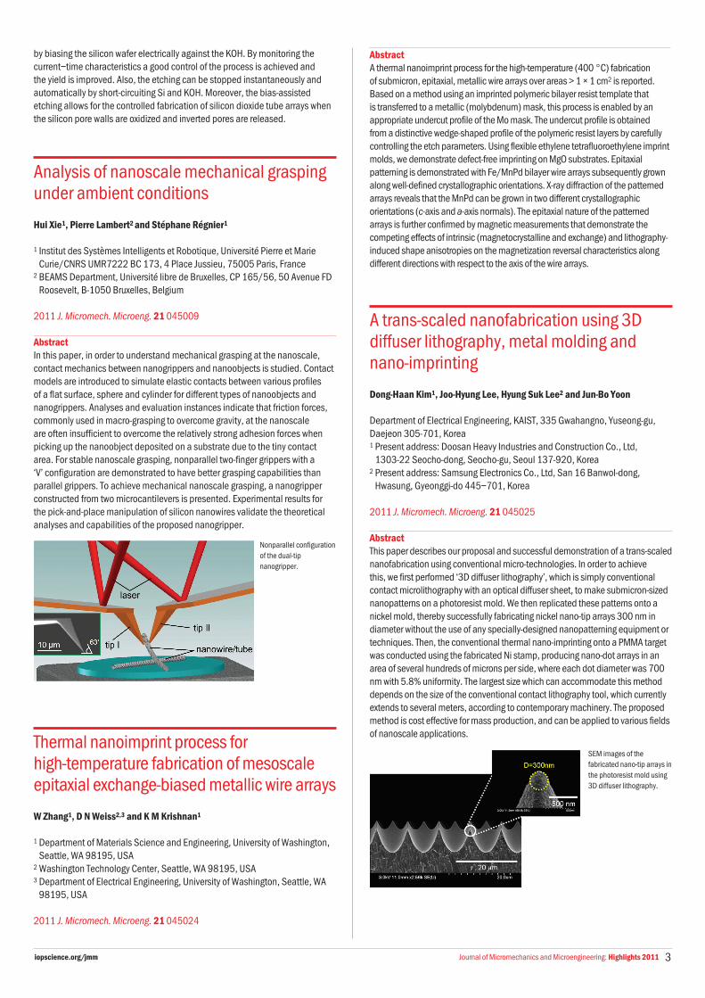
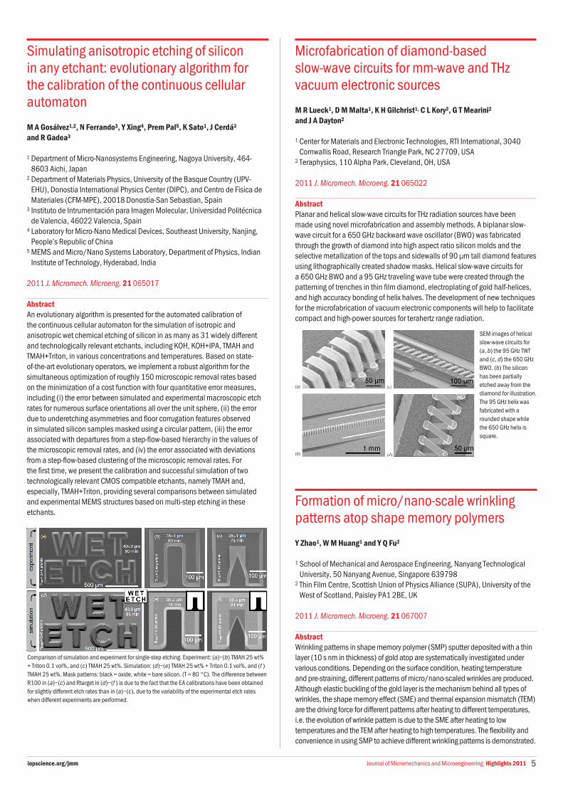
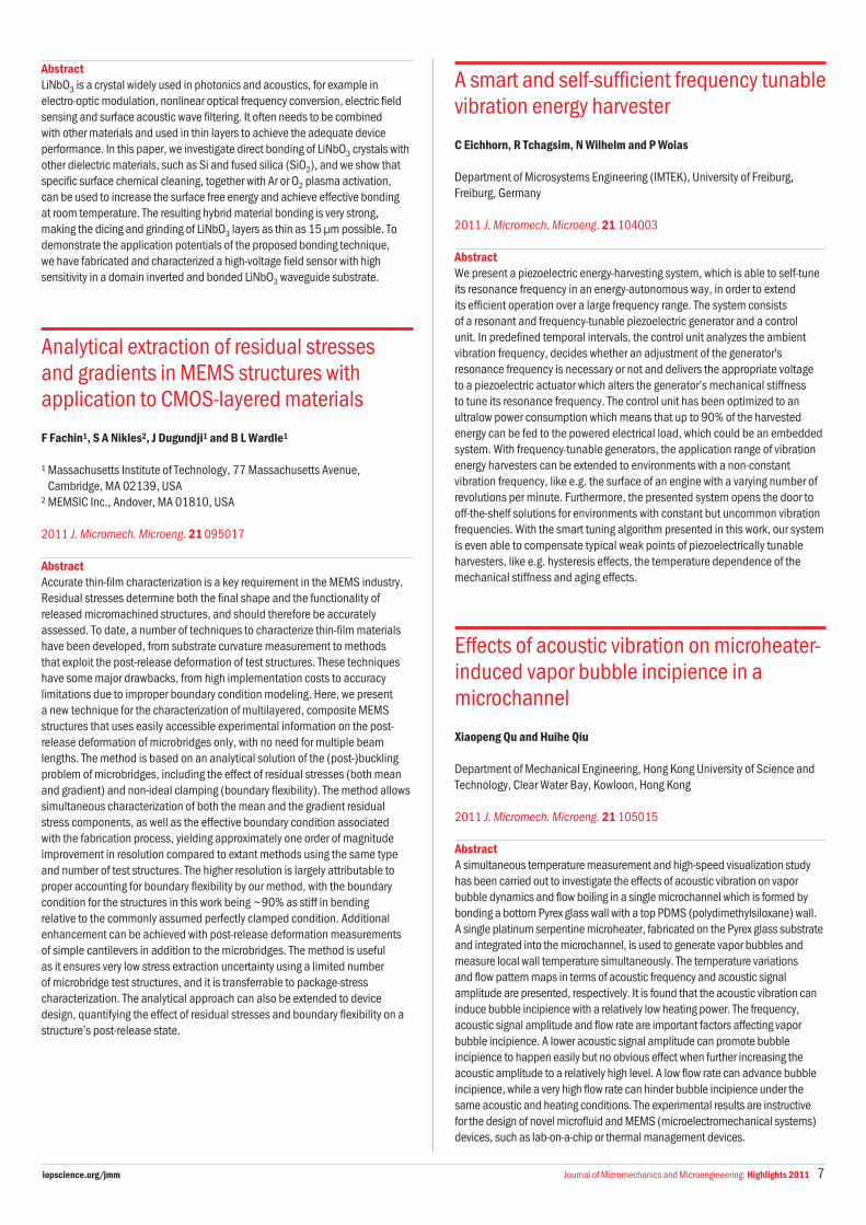
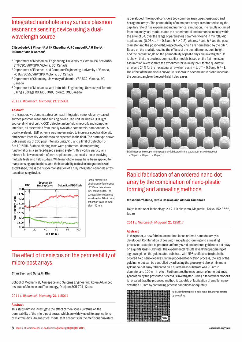