Embed Size (px)
DESCRIPTION
crash. quantum physics. Atomic, materials, chemistry modeling. device modeling < 50nm (1000 atoms). Semi-classical device modeling. device parameters. Towards parameter-free device modeling. Jesse Maassen (Supervisor : Prof. Hong Guo) - PowerPoint PPT Presentation
Citation preview
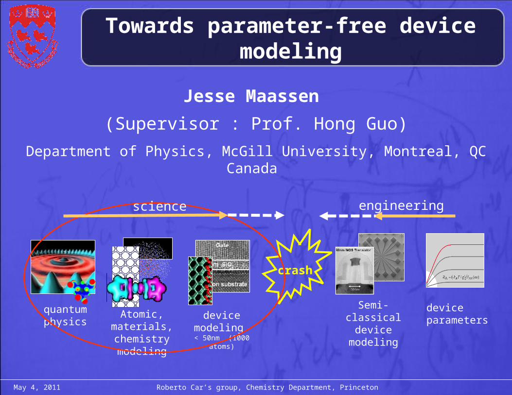
Jesse Maassen
(Supervisor : Prof. Hong Guo)Department of Physics, McGill University, Montreal, QC Canada
Semi-classical device
modeling
device parametersAtomic, materials,
chemistry modeling
quantum physics device modeling < 50nm (1000 atoms)
crash
science engineering
May 4, 2011 Roberto Car’s group, Chemistry Department, Princeton
Towards parameter-free device modeling
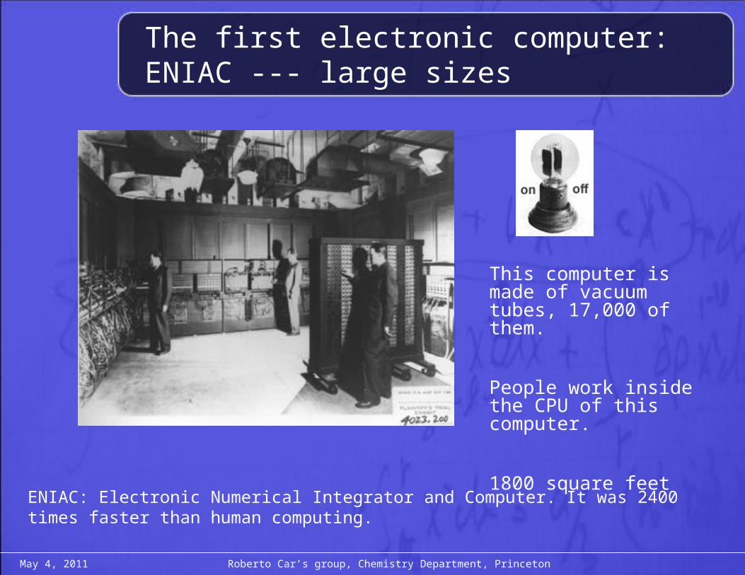
The first electronic computer: ENIAC --- large sizes
This computer is made of vacuum tubes, 17,000 of them.
People work inside the CPU of this computer.
1800 square feet
ENIAC: Electronic Numerical Integrator and Computer. It was 2400 times faster than human computing.
May 4, 2011 Roberto Car’s group, Chemistry Department, Princeton

Today: transistors are very small
200 million transistors can fit on each of these pin head.
€
1960 : L ≈10μm
2000 : L ≈100nm
2010 : L = 22nm
How to compute charge conduction in these atomic systems?
Line of ~ 50 atoms
May 4, 2011 Roberto Car’s group, Chemistry Department, Princeton
As the size of a device goes down, physics change
Channel Length, L
1 mm
0.1 mm
10 µm
1 µ m
0.1 µm
10 nm
1 nm
0.1 nm
Transistor
2000
Atomic dimensions
1975
2016
Top
Bottom
Macroscopicdimensions
L
May 4, 2011 Roberto Car’s group, Chemistry Department, Princeton
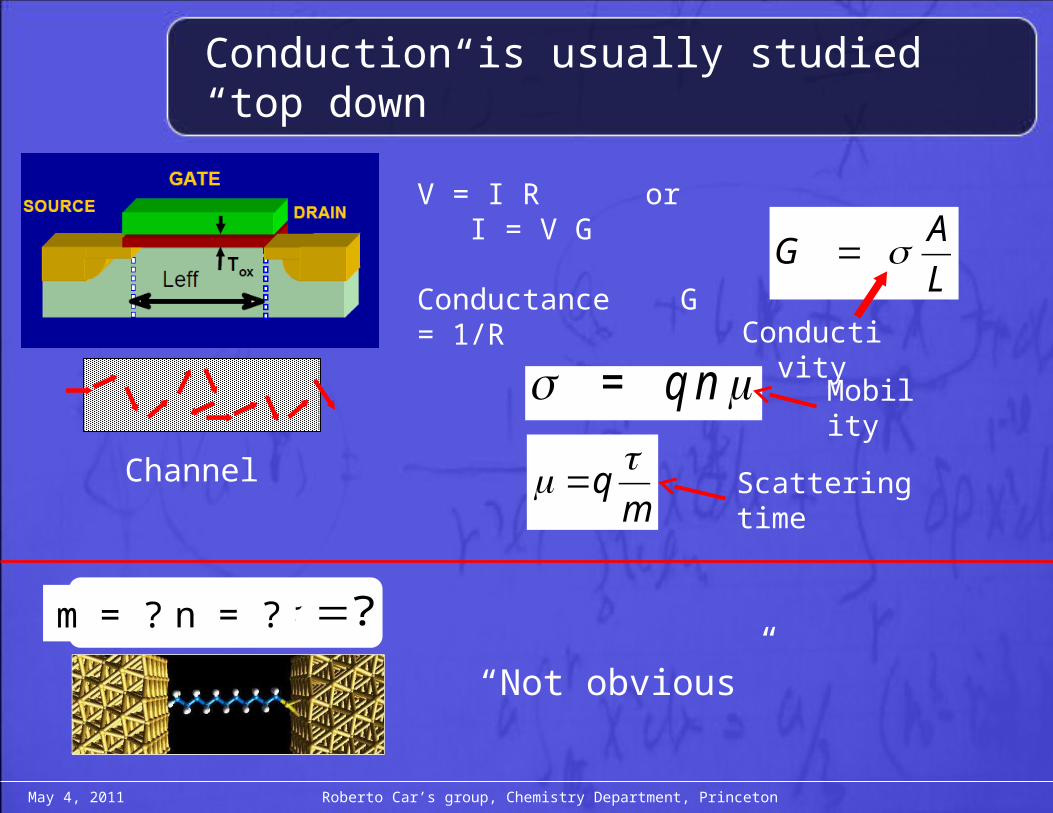
V = I R or I = V G
Conductance G = 1/R L
AG σ=
Conductivity
“Not obvious”
Conduction is usually studied “top down”
μσ nq= Mobility
?=τm = ? n = ?
mqτμ = Scattering timeChannel
May 4, 2011 Roberto Car’s group, Chemistry Department, Princeton

What device parameters?
⎟⎟⎟⎟
⎠
⎞
⎜⎜⎜⎜
⎝
⎛
⎟⎟⎟
⎠
⎞
⎜⎜⎜
⎝
⎛=
⎟⎟⎟⎟
⎠
⎞
⎜⎜⎜⎜
⎝
⎛
VVV
III
G
S
D
G
S
DDevice
parameters
These parameters specify properties of each individual device.
How to obtain device parameters? --- by experimental measurements - now; --- by computational modeling;
May 4, 2011 Roberto Car’s group, Chemistry Department, Princeton
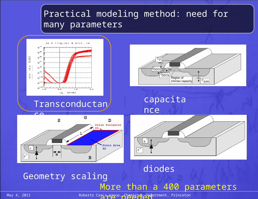
Practical modeling method: need for many parameters
capacitanceTransconductance
Geometry scalingdiodes
More than a 400 parameters are needed.May 4, 2011 Roberto Car’s group, Chemistry Department, Princeton

Moore’s law for model parameters
Number of parameter double every 18 months
Reflects the complexity in modern technology
103
Year of introduction
Implem
ented feature(arbitrary unit in log scale)
1
102
10
1965 1980 1990 2000
Level 1
Level 2
Level 3
BSIM1
BSIM2
BSIM3v3
BSIM4
Num
ber
of p
aram
eter
s
parameter per feature
PSP
May 4, 2011 Roberto Car’s group, Chemistry Department, Princeton

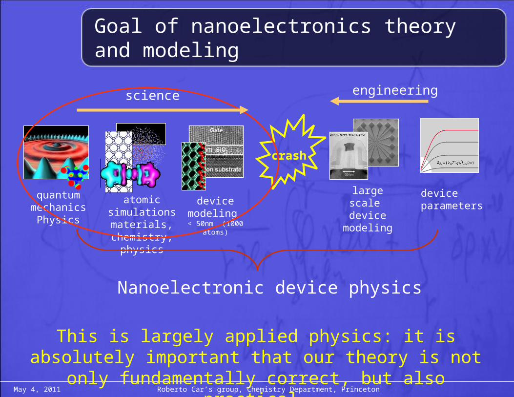
Different modeling method: includes quantum and discrete material properties (all parameter free, no m, n or τ)
Quantum:
Tunneling – cannot turn off transistor; Size quantization ; electron-phonon scattering during current flow; Quantum dissipation; Spin transport; Spin-orbital effects …
Atomistic structures:
Materials are no longer a continuous medium. Atomic simulations are useful when: more atomic species are used in nano-systems; charge transfer; interfaces, surfaces, domain boundaries; external potential drop; disorder …
It is highly desirable to develop parameter-free theory and modeling method.
May 4, 2011 Roberto Car’s group, Chemistry Department, Princeton
large scale device
modeling
device parametersatomic simulations
materials, chemistry, physics
quantum mechanics Physics
device modeling < 50nm (1000 atoms)
Nanoelectronic device physics
crash
science engineering
Goal of nanoelectronics theory and modeling
This is largely applied physics: it is absolutely important that our theory is not only fundamentally correct, but also practical.
May 4, 2011 Roberto Car’s group, Chemistry Department, Princeton

Basic ingredients of a theory:
Picture from: Nitzan & Ratner, Science, 300, 1384 (2003).
1. A transport model
2. Device Hamiltonian
3. Non-equilibrium Physics
4. Transmission
5. Fermi level alignment
6. Calculable!
May 4, 2011 Roberto Car’s group, Chemistry Department, Princeton
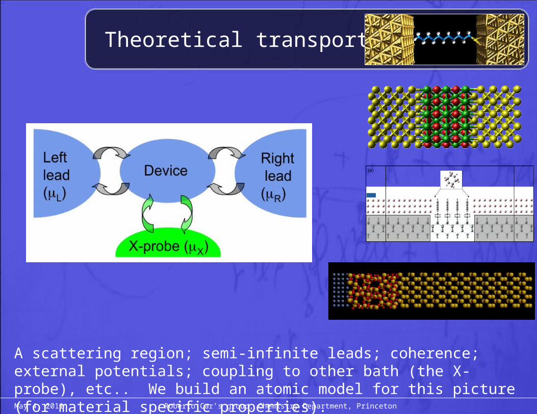
Theoretical transport model
A scattering region; semi-infinite leads; coherence; external potentials; coupling to other bath (the X-probe), etc.. We build an atomic model for this picture (for material specific properties).
May 4, 2011 Roberto Car’s group, Chemistry Department, Princeton
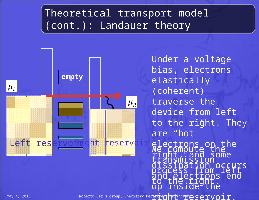
Theoretical transport model (cont.): Landauer theory
Under a voltage bias, electrons elastically (coherent) traverse the device from left to the right. They are “hot” electrons on the right, and some dissipation occurs and electrons end up inside the right reservoir.
We compute the transmission process from left to the right.
Left reservoir
Lμ
Rμ
empty
Right reservoir
May 4, 2011 Roberto Car’s group, Chemistry Department, Princeton

Device Hamiltonian
The Hamiltonian determines the energy levels of the device. (How to fill these levels non-equilibrium statistics.)
What kind of H to use is an issue of accuracy (tight-binding, DFT, GW, …).
In the end, we want to compare our results with experimental data without adjusting theoretical parameters.
DFT offers a good trade-off between accuracy and speed.
H = Hleads + Hdevice + Hcoupling
May 4, 2011 Roberto Car’s group, Chemistry Department, Princeton

Density functional theory : Kohn-Sham Hamiltonian
QuickTime™ and aTIFF (Uncompressed) decompressor
are needed to see this picture.
Hamiltonian
Potential of ions
Potential of electrons
(Poisson equation)
Quantum/ many-body effects
Assumption : All electrons are independent
May 4, 2011 Roberto Car’s group, Chemistry Department, Princeton
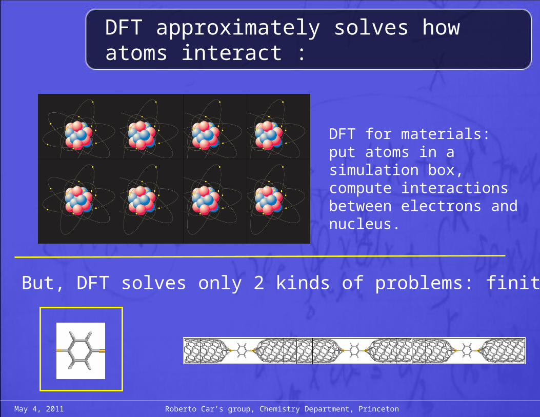
DFT approximately solves how atoms interact :
DFT for materials: put atoms in a simulation box, compute interactions between electrons and nucleus.
But, DFT solves only 2 kinds of problems: finite or periodic systems.
May 4, 2011 Roberto Car’s group, Chemistry Department, Princeton
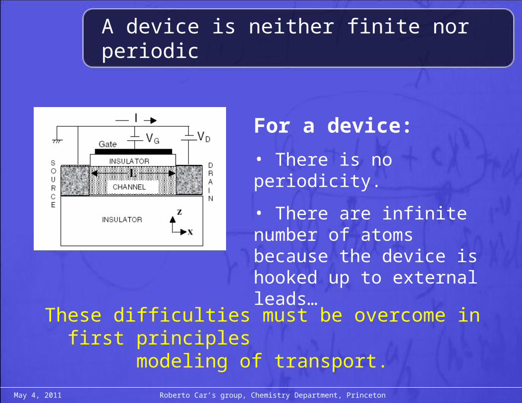
A device is neither finite nor periodic
For a device:
• There is no periodicity.
• There are infinite number of atoms because the device is hooked up to external leads…
These difficulties must be overcome in first principles modeling of transport.
May 4, 2011 Roberto Car’s group, Chemistry Department, Princeton
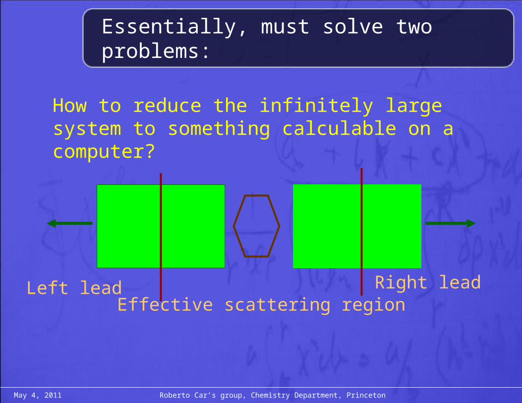
Essentially, must solve two problems:
Effective scattering regionLeft lead Right lead
How to reduce the infinitely large system to something calculable on a computer?
May 4, 2011 Roberto Car’s group, Chemistry Department, Princeton
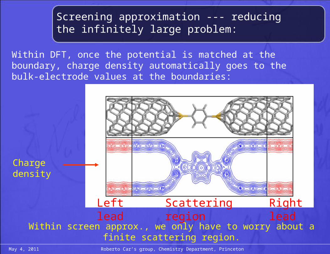
Screening approximation --- reducing the infinitely large problem:
Within DFT, once the potential is matched at the boundary, charge density automatically goes to the bulk-electrode values at the boundaries:
Within screen approx., we only have to worry about a finite scattering region.
Charge density
Left lead Right leadScattering region
May 4, 2011 Roberto Car’s group, Chemistry Department, Princeton

Another example
Using the screening approximation and solving Poisson Equation in real space, we can deal with systems with different leads.
May 4, 2011 Roberto Car’s group, Chemistry Department, Princeton
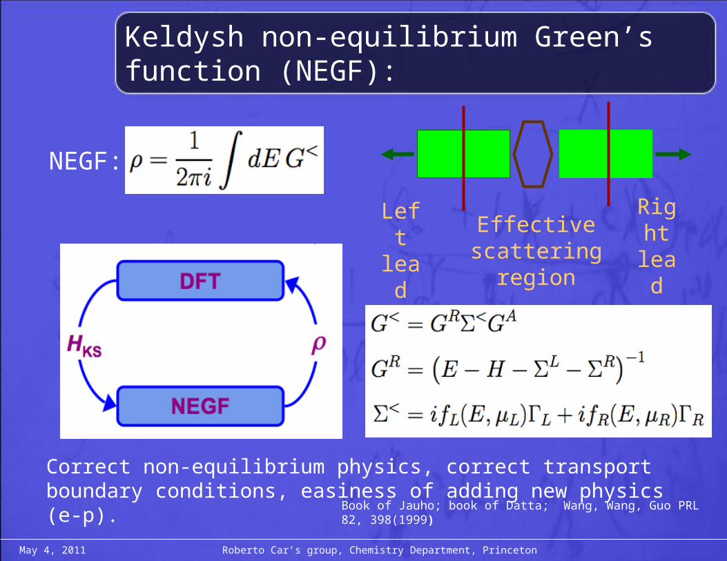
Keldysh non-equilibrium Green’s function (NEGF):
Book of Jauho; book of Datta; Wang, Wang, Guo PRL 82, 398(1999)
NEGF:
Correct non-equilibrium physics, correct transport boundary conditions, easiness of adding new physics (e-p).
Effective scattering region
Left lead
Right lead
May 4, 2011 Roberto Car’s group, Chemistry Department, Princeton
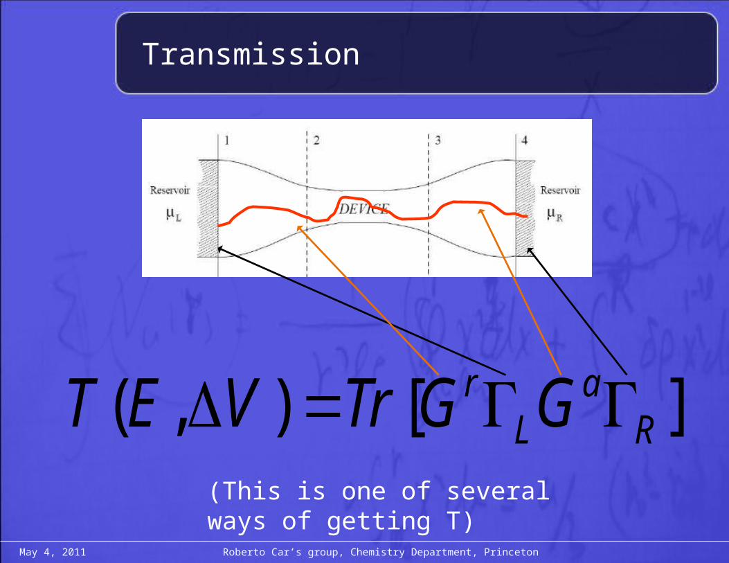
Transmission
][),( Ra
Lr GGTrVET ΓΓ=Δ
(This is one of several ways of getting T)
May 4, 2011 Roberto Car’s group, Chemistry Department, Princeton

NEGF-DFT: Taylor, Guo and Wang, PRB 63, 245407 (2001).
Use density functional theory (DFT) to compute the electronic structure and all other materials properties of the open device structure;
Use Keldysh non-equilibrium Green’s function (NEGF) to populate the electronic states (non-equilibrium quantum statistics);
Use numerical techniques to deal with the open boundary conditions.
Molecular transport junctionsSolid state devices
May 4, 2011 Roberto Car’s group, Chemistry Department, Princeton

Wide range of research has been carried out by NEGF-DFT
• Leakage current in MOSFET;• Transport in semiconductor devices, photocells;• Transport in carbon nanostructures;• Resistivity of Cu interconnects; • Conductance, I-V curves of molecular transport junctions;• Computation of capacitance, diodes, inductance, current density;• TMR, spin currents, and spin injection in magnetic tunnel junctions;• Transport in nanowires, rods, films, clusters, nanotubes;• Resistance of surface, interface, grain boundaries;• STM image simulations;• Strongly correlated electrons in transport;• Transport through short peptides;• ….
it is a progressing field and not all is perfect yet.
Recently developed modeling tool allows for:
Large-scale systems (~1000 atoms & ~10 nm).
Disorder: Surface/interface roughness, dopants, impurities.
May 4, 2011 Roberto Car’s group, Chemistry Department, Princeton
An example:
• Graphene-metal interface
May 4, 2011 Roberto Car’s group, Chemistry Department, Princeton
May 4, 2011 Roberto Car’s group, Chemistry Department, Princeton
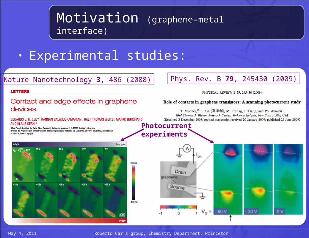
• Experimental studies:
Nature Nanotechnology 3, 486 (2008) Phys. Rev. B 79, 245430 (2009)
Photocurrentexperiments
Motivation (graphene-metal interface)

May 4, 2011 Roberto Car’s group, Chemistry Department, Princeton
Parameter-free transport (NEGF-DFT*) calculation of a
graphene / metal interface
* Jeremy Taylor, Hong Guo and Jian Wang, PRB 63, 245407 (2001).
Our goal
May 4, 2011 Roberto Car’s group, Chemistry Department, Princeton
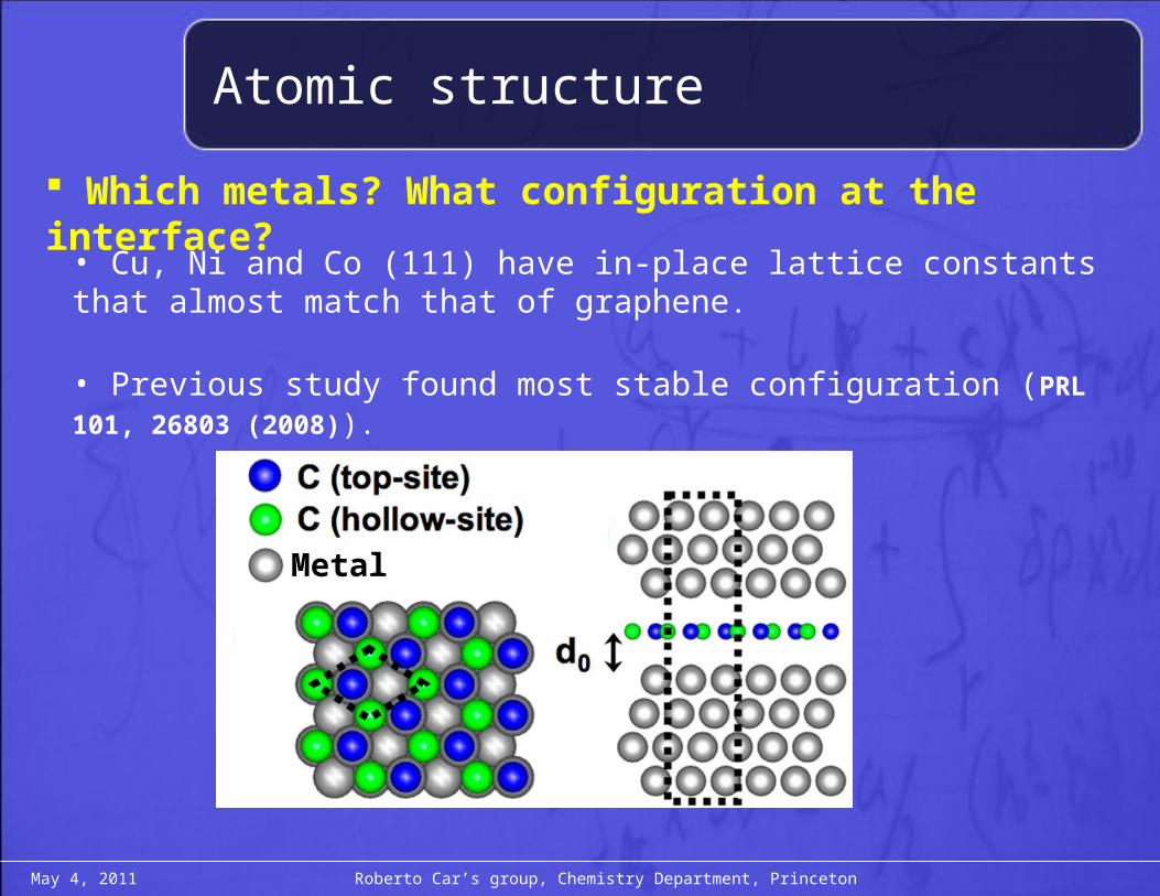
Which metals? What configuration at the interface?
• Cu, Ni and Co (111) have in-place lattice constants that almost match that of graphene.
• Previous study found most stable configuration (PRL 101, 26803 (2008)).
Metal
Atomic structure

Graphene-Cu interface
May 4, 2011 Roberto Car’s group, Chemistry Department, Princeton
Appl. Phys. Lett. 97, 142105 (2010)
Bandstructure of hybrid
graphene | Cu(111) system
Graphene states in black Weak hybridization n-type graphene
Metal

Graphene-Cu interface
Transport properties: graphene-Cu(111) system
Appl. Phys. Lett. 97, 142105 (2010)
May 4, 2011 Roberto Car’s group, Chemistry Department, Princeton
Double minimum T.
T almost perfectly described by pure graphene at TMIN.
Graphene-Cu interface
Transport properties: graphene-Cu(111) system
• One Dirac point pinned, while other moves with V.
QuickTime™ and aTIFF (Uncompressed) decompressor
are needed to see this picture.
• Peak in conductance doping level of graphene
Appl. Phys. Lett. 97, 142105 (2010)
May 4, 2011 Roberto Car’s group, Chemistry Department, Princeton

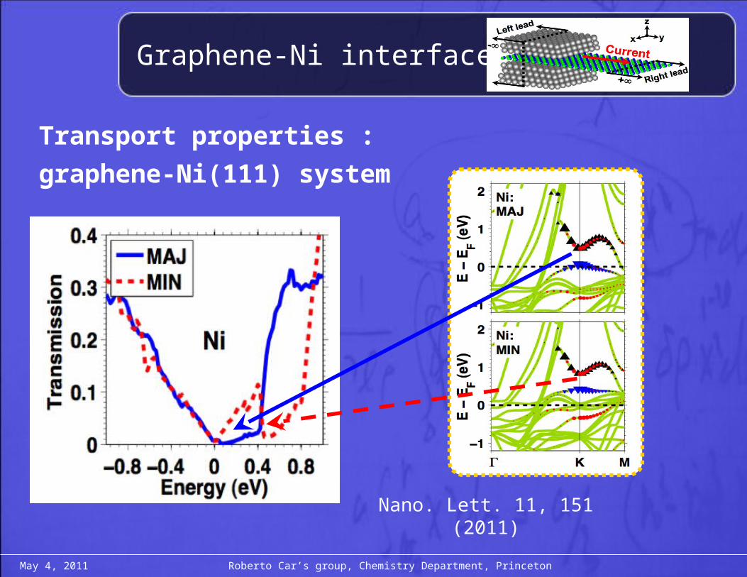
Graphene-Ni interface
Band structure : graphene-Ni(111) system
• Strong hybridization with metal
• Band gap opening
• Graphene is spin-polarized
: A-site C(pz): B-site C(pz)
: Ni(dZ2)
Nano. Lett. 11, 151 (2011)
May 4, 2011 Roberto Car’s group, Chemistry Department, Princeton
Graphene-Ni interface
Nano. Lett. 11, 151 (2011)
May 4, 2011 Roberto Car’s group, Chemistry Department, Princeton
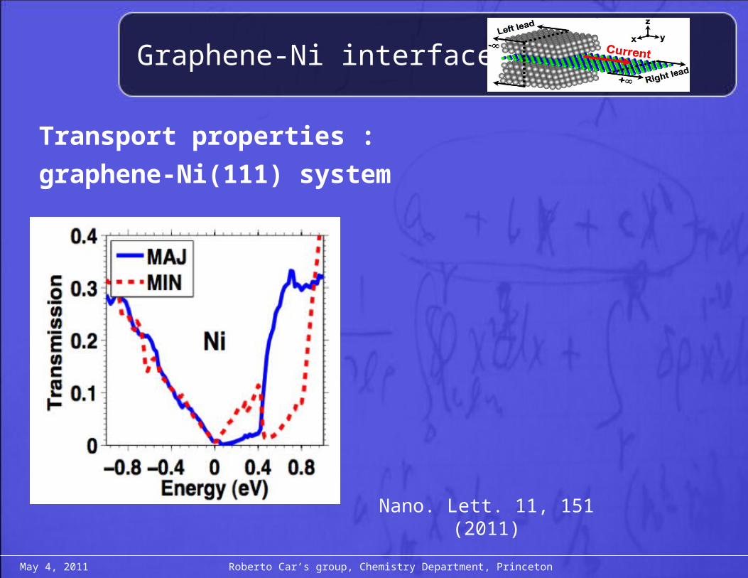
Transport properties :
graphene-Ni(111) system
Graphene-Ni interface
Nano. Lett. 11, 151 (2011)
May 4, 2011 Roberto Car’s group, Chemistry Department, Princeton
Transport properties :
graphene-Ni(111) system
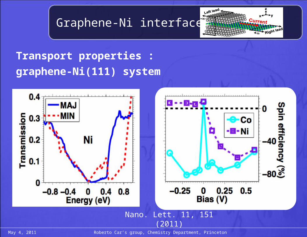
Graphene-Ni interface
Nano. Lett. 11, 151 (2011)
May 4, 2011 Roberto Car’s group, Chemistry Department, Princeton
Transport properties :
graphene-Ni(111) system
Graphene-metal interface
May 4, 2011 Roberto Car’s group, Chemistry Department, Princeton
Cu merely n-dopes the graphene resulting in:
• Peak in dI/dV provides doping level
• Can be simply modeled assuming a n-i junction
• Similar trends for Al, Ag, Au & Pt
Ni & Co create spin-dependent (pseudo-) band gaps in
graphene.
• Large spin injection efficiencies ~80%
SUMMARY
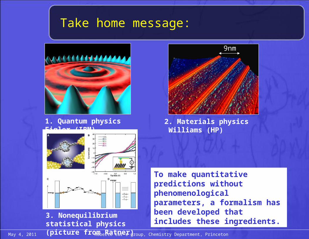
1. Quantum physics Eigler (IBM)
9nm
2. Materials physics Williams (HP)
3. Nonequilibrium statistical physics (picture from Ratner)
To make quantitative predictions without phenomenological parameters, a formalism has been developed that includes these ingredients.
Take home message:
May 4, 2011 Roberto Car’s group, Chemistry Department, Princeton

Thank you !(and to my supervisor and colleagues)
$: NSERC, FQRNT, CIFAR, DRDC; Computers :
SRC, LuXin Energy. RQCHP,CLUMEQ
May 4, 2011 Roberto Car’s group, Chemistry Department, Princeton
Another example:
• Graphene-metal interface
• Ultrathin Si films
May 4, 2011 Roberto Car’s group, Chemistry Department, Princeton

May 4, 2011 Roberto Car’s group, Chemistry Department, Princeton
The main motivation for our research was the experimental work by Pengpeng Zhang et al. with silicon-on-insulators.
QuickTime™ and aTIFF (LZW) decompressor
are needed to see this picture.
QuickTime™ and aTIFF (LZW) decompressor
are needed to see this picture.
Nature 439, 703 (2006)
SiO2
QuickTime™ and aTIFF (LZW) decompressor
are needed to see this picture.
SiSiO2Vacuum
Charge traps
Used STM to image 10 nm Si film on SiO2
Surfacestates
Motivation (Si nano-film)
QuickTime™ and aTIFF (LZW) decompressor
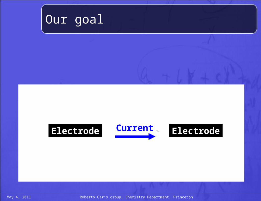
are needed to see this picture.CurrentElectrode Electrode
Our goal
May 4, 2011 Roberto Car’s group, Chemistry Department, Princeton

QuickTime™ and aTIFF (LZW) decompressor
are needed to see this picture.
Length
Th
ickn
ess
Surface
CurrentElectrode Electrode
Doping level(lead or channel)
Orientation
Our goal
May 4, 2011 Roberto Car’s group, Chemistry Department, Princeton
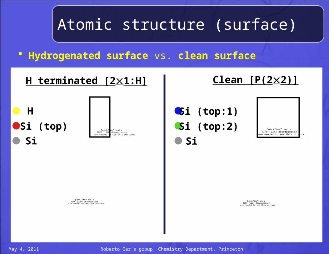
Hydrogenated surface vs. clean surface
QuickTime™ and aTIFF (LZW) decompressor
are needed to see this picture.
QuickTime™ and aTIFF (LZW) decompressor
are needed to see this picture.
QuickTime™ and aTIFF (LZW) decompressor
are needed to see this picture.
QuickTime™ and aTIFF (LZW) decompressor
are needed to see this picture.
H
Si (top)
Si
Si (top:1)
Si (top:2)
Si
H terminated [21:H] Clean [P(22)]
May 4, 2011 Roberto Car’s group, Chemistry Department, Princeton
Atomic structure (surface)
May 4, 2011 Roberto Car’s group, Chemistry Department, Princeton
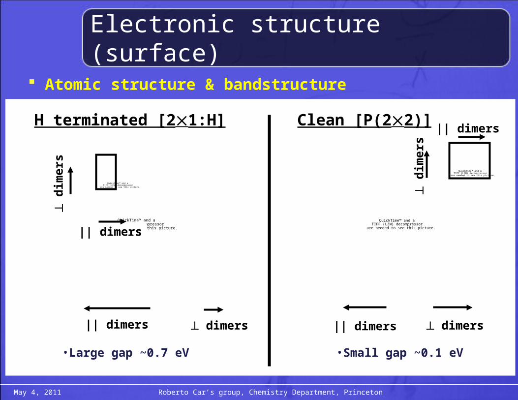
Atomic structure & bandstructure
H terminated [21:H] Clean [P(22)]
|| dimers dimers || dimers dimers
•Large gap ~0.7 eV •Small gap ~0.1 eV
QuickTime™ and aTIFF (LZW) decompressor
are needed to see this picture.
QuickTime™ and aTIFF (LZW) decompressor
are needed to see this picture.
d
imer
s
|| dimersQuickTime™ and a
TIFF (LZW) decompressorare needed to see this picture.
QuickTime™ and aTIFF (LZW) decompressor
are needed to see this picture.
|| dimers
d
imer
s
Electronic structure (surface)
QuickTime™ and aTIFF (LZW) decompressor
are needed to see this picture.
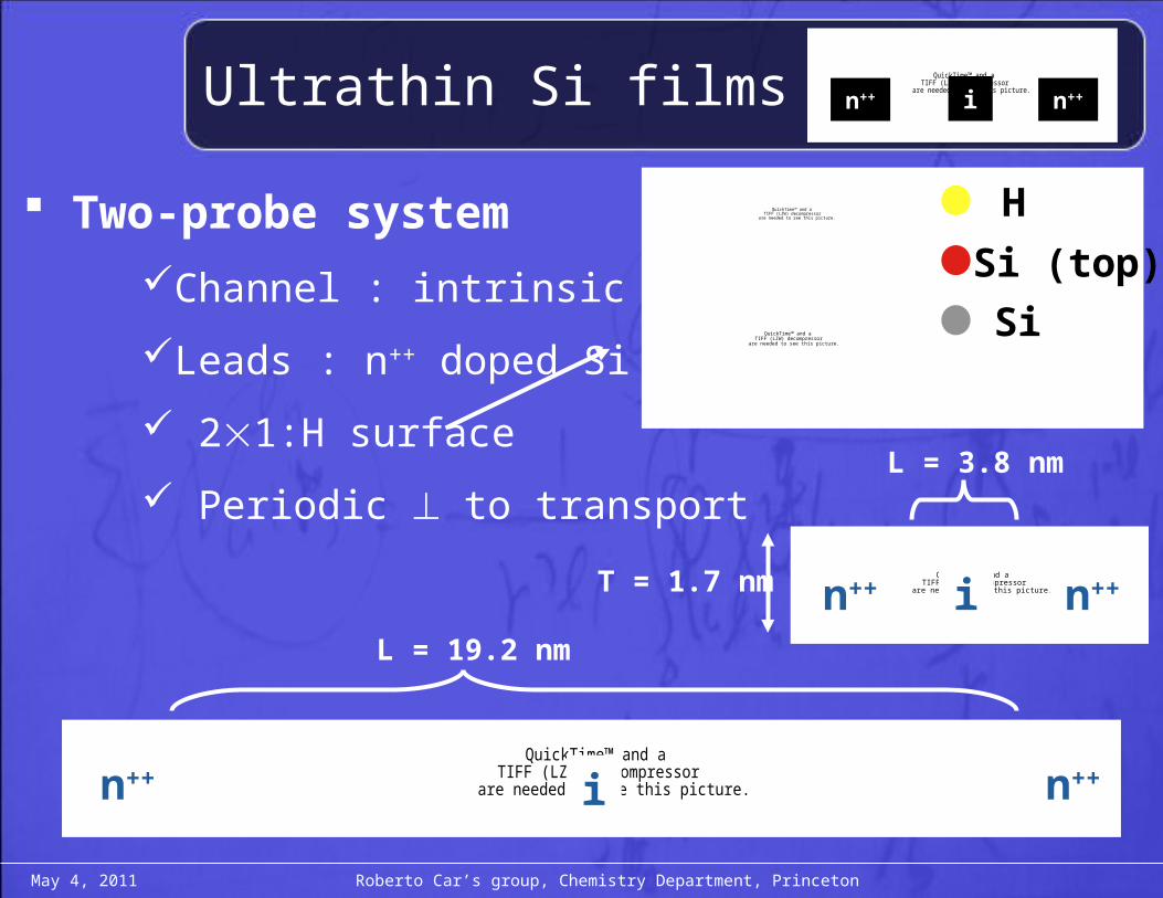
n++ n++iUltrathin Si films
QuickTime™ and aTIFF (LZW) decompressor
are needed to see this picture.
QuickTime™ and aTIFF (LZW) decompressor
are needed to see this picture.H
Si (top)
Si
Two-probe system
Channel : intrinsic Si
Leads : n++ doped Si
21:H surface
Periodic to transport
QuickTime™ and aTIFF (LZW) decompressor
are needed to see this picture.n++ n++i
L = 19.2 nm
QuickTime™ and aTIFF (LZW) decompressor
are needed to see this picture.n++ n++i
L = 3.8 nm
T = 1.7 nm
May 4, 2011 Roberto Car’s group, Chemistry Department, Princeton
QuickTime™ and aTIFF (LZW) decompressor
are needed to see this picture.
n++ n++i
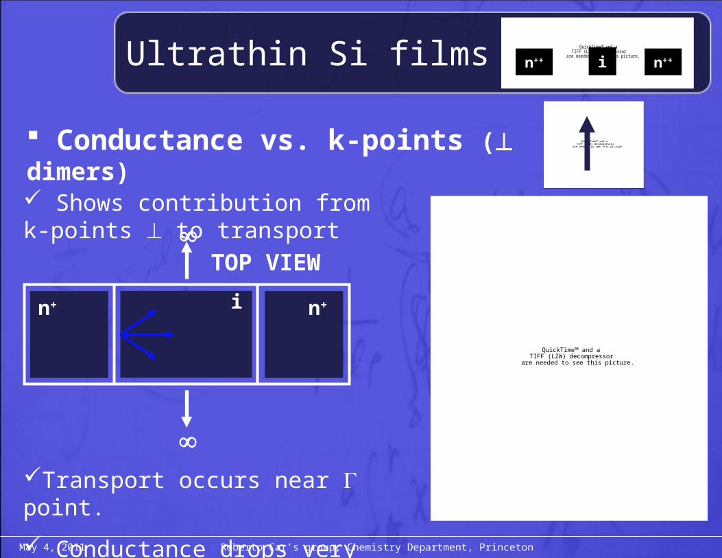
Conductance vs. k-points ( dimers)
Shows contribution from k-points to transport
Transport occurs near Γ point.
Conductance drops very rapidly
QuickTime™ and aTIFF (LZW) decompressor
are needed to see this picture.
in+ n+
QuickTime™ and aTIFF (LZW) decompressor
are needed to see this picture.
TOP VIEW
Ultrathin Si films
May 4, 2011 Roberto Car’s group, Chemistry Department, Princeton
QuickTime™ and aTIFF (LZW) decompressor
are needed to see this picture.
n++ n++i
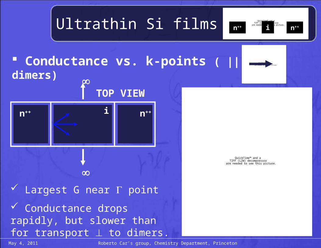
Conductance vs. k-points ( || dimers)
Largest G near Γ point
Conductance drops rapidly, but slower than for transport to dimers.
QuickTime™ and aTIFF (LZW) decompressor
are needed to see this picture.
in++ n++
TOP VIEW
QuickTime™ and aTIFF (LZW) decompressor
are needed to see this picture.
Ultrathin Si films
May 4, 2011 Roberto Car’s group, Chemistry Department, Princeton
QuickTime™ and aTIFF (LZW) decompressor
are needed to see this picture.
n++ n++i
QuickTime™ and aTIFF (LZW) decompressor
are needed to see this picture.
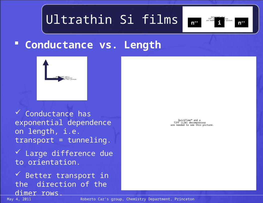
Conductance vs. Length
Conductance has exponential dependence on length, i.e. transport = tunneling.
Large difference due to orientation.
Better transport in the direction of the dimer rows.
QuickTime™ and aTIFF (LZW) decompressor
are needed to see this picture.
Ultrathin Si films
May 4, 2011 Roberto Car’s group, Chemistry Department, Princeton

QuickTime™ and aTIFF (LZW) decompressor
are needed to see this picture.
n++ n++iUltrathin Si films
May 4, 2011 Roberto Car’s group, Chemistry Department, Princeton
Electronic structure
• 21:H [~0.7 eV gap]
• p(22) [~0.1 eV gap]
Transport properties
• Large effect of orientation in G for 21:H
More complete study to come soon!
SUMMARY
Some (more) examples:
Effect of dephasing on electron transport
Scattering properties of a nano-electromechanical system [Published in Phys. Rev. Lett. 105, 217206 (2010)]
Raman spectra of graphene on Cu substrate [Submitted to Phys. Rev. Lett.]
Effect of disorder and vacancies on electronic transport through a Au conductor [in progress]
Electron transport through a Si/Ge interface [in progress]

Effect of dephasing on electron transport
• Phase breaking : Phenomenological model (Buttiker probe model)
• Self-energy : Simple implementation
J. Maassen, F. Zahid and H. Guo PRB 80, 125423 (2009)
I(μX) = 0

Effect of dephasing on electron transport
Al - BDT - Al
Left reservoir
Right reservoir
Lμ
Rμ
J. Maassen, F. Zahid and H. Guo PRB 80, 125423 (2009)
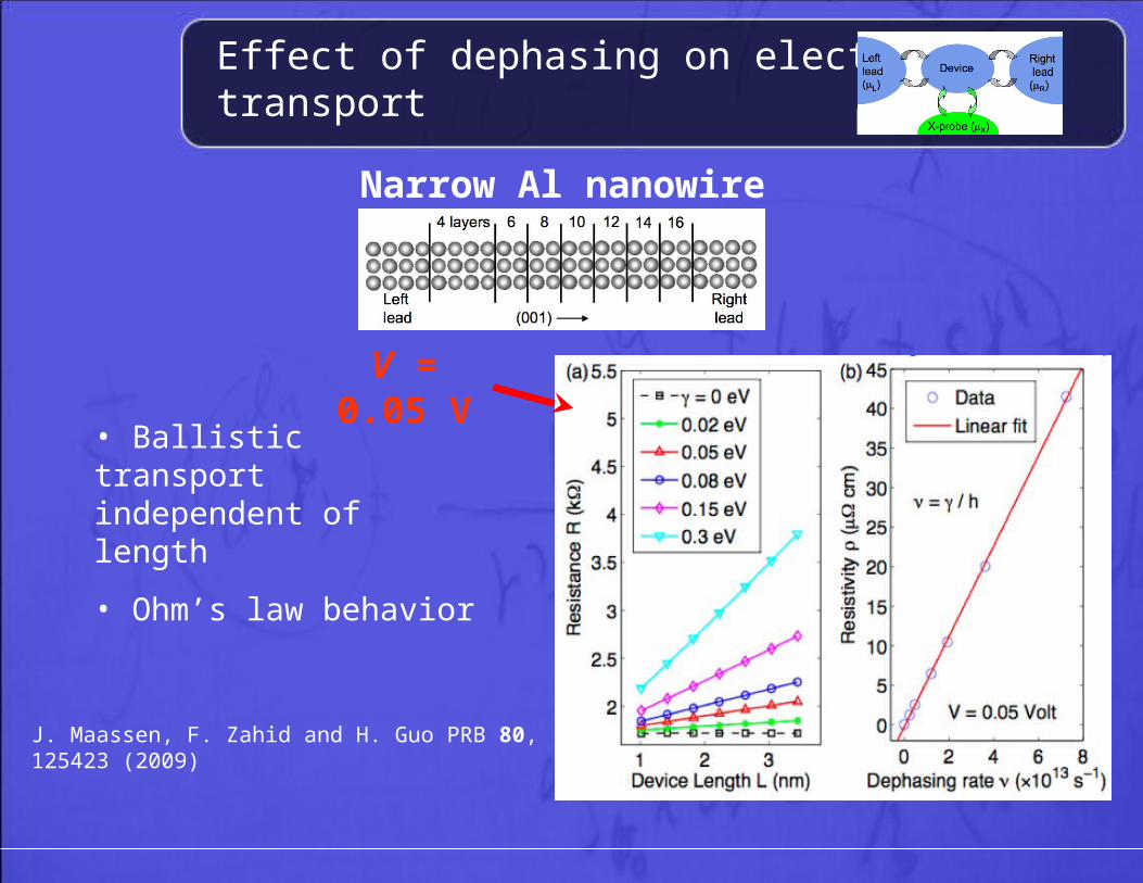
Effect of dephasing on electron transport
Narrow Al nanowire
• Ballistic transport independent of length
• Ohm’s law behavior
V = 0.05 V
J. Maassen, F. Zahid and H. Guo PRB 80, 125423 (2009)