Embed Size (px)
Citation preview

Hot Chips 15
August 2003Janus – A Gigaflops RISC+VLIW SoC TilePier S. PAOLUCCI 1
Janus – A Gigaflop RISC + VLIW SoC Tile
Pier S. PAOLUCCI a,b,*, Ben ALTIERI a, Federico AGLIETTI a, Stefano V. BASILE a, Piergiovanni BAZZANA a, Sergio BRUZZONE a,
Alessandro CATASTA a, Antonio CERRUTO a, Maurizio COSIMI a, Yves FUSELLA d, Philippe KAJFASZ c, Andrea MICHELOTTI a,
Elena PASTORELLI a, Silvia PIRIA a, Enrico REMONDINI a, Andrea RICCIARDI a, Fabrizio ROSCIARELLI a
– a IPITEC srl, an ATMEL Company, Via Vito Giuseppe Galati 87, 00155 Roma, Italy
– b INFN Roma, Dip. Fisica Uni. Roma “La Sapienza”, P.le Aldo Moro 5, 00185 Roma, Italy
– c THALES Communications 66, rue du Fossé Blanc – BP 156 - 92231 Gennevilliers Cedex, France
– d ATMEL, Zone Industrielle 13106 Rousset cedex, France
– *Corresponding author: [email protected] (Pier Stanislao PAOLUCCI)

Hot Chips 15
August 2003Janus – A Gigaflops RISC+VLIW SoC TilePier S. PAOLUCCI 2
Agenda (1/2)
mAgic™ DSP VLIW Core– Complex Domain, 40-bit Floating Point VLIW DSP Core, 15 ops/cycle– Automatic VLIW Scheduling– Dynamic Program Decompression– Low clock, high ILP core: 1.0 Gigaflops @ 100 MHz, 180 nm CMOS– SoC interface
Janus ™ = ARM7 + mAgic VLIW DSP Core– Audio Beam-forming, Physical Modeling– Architecture, Floor-plan, Technological results (180 nm CMOS)

Hot Chips 15
August 2003Janus – A Gigaflops RISC+VLIW SoC TilePier S. PAOLUCCI 3
Agenda (2/2)
Dimensional Analysis for Deep Sub-Micron (DSM) VLIW tile design methodology for high performance at moderate clock speed– ILP*frequency vs. Wire Delay balance on present and future designs– Memory area vs. Operator Area on present and future designs – Validation of the dimensional analysis using mAgic detailed Gate
Counts and Technological Implementation feedbacks.– Tiles for Short Wires:
RISC+VLIW Tile for SoC on future DSM designs
Hypothesis for a 90 nm multiple tile design

Hot Chips 15
August 2003Janus – A Gigaflops RISC+VLIW SoC TilePier S. PAOLUCCI 4
mAgic™ DSP Core
1.0 Gigaflops @ 100 MHz, 15 ops/cycleComplex Domain, 40-bit Floating Point VLIW DSP CoreSeamless VLIW: from linear assembler to VLIW schedulingDyProDe: Dynamic Program Decompression: 4 PM bit/opLow clock, high ILP core: easier SoC Design Closure, less internal pipelines (no need for custom operators), higher efficiency on applicationsMemory mapped slave on the controller’s system bus
Expected dissipation: less than 500mW (typical)
2.4X the performance or 41% the clock at 40 bit vs. classical 32-bit stand-alone floating point DSP
Hot Chips 15
August 2003Janus – A Gigaflops RISC+VLIW SoC TilePier S. PAOLUCCI 5
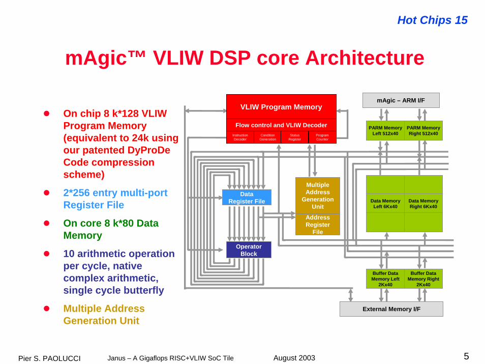
mAgic™ VLIW DSP core Architecture
mAgic – ARM I/F
PARM MemoryLeft 512x40
PARM MemoryRight 512x40
Data MemoryLeft 6Kx40
Data MemoryRight 6Kx40
Buffer Data Memory Left
2Kx40
Buffer Data Memory Right
2Kx40
External Memory I/F
Multiple Address
GenerationUnit
Address Register
File
Operator Block
Data Register File
VLIW Program Memory
Flow control and VLIW DecoderInstruction Decoder
Condition Generation
Status Register
Program Counter
On chip 8 k*128 VLIW Program Memory (equivalent to 24k using our patented DyProDe Code compressionscheme)
2*256 entry multi-port Register File
On core 8 k*80 Data Memory
10 arithmetic operation per cycle, native complex arithmetic, single cycle butterfly
Multiple AddressGeneration Unit
Hot Chips 15
August 2003Janus – A Gigaflops RISC+VLIW SoC TilePier S. PAOLUCCI 6
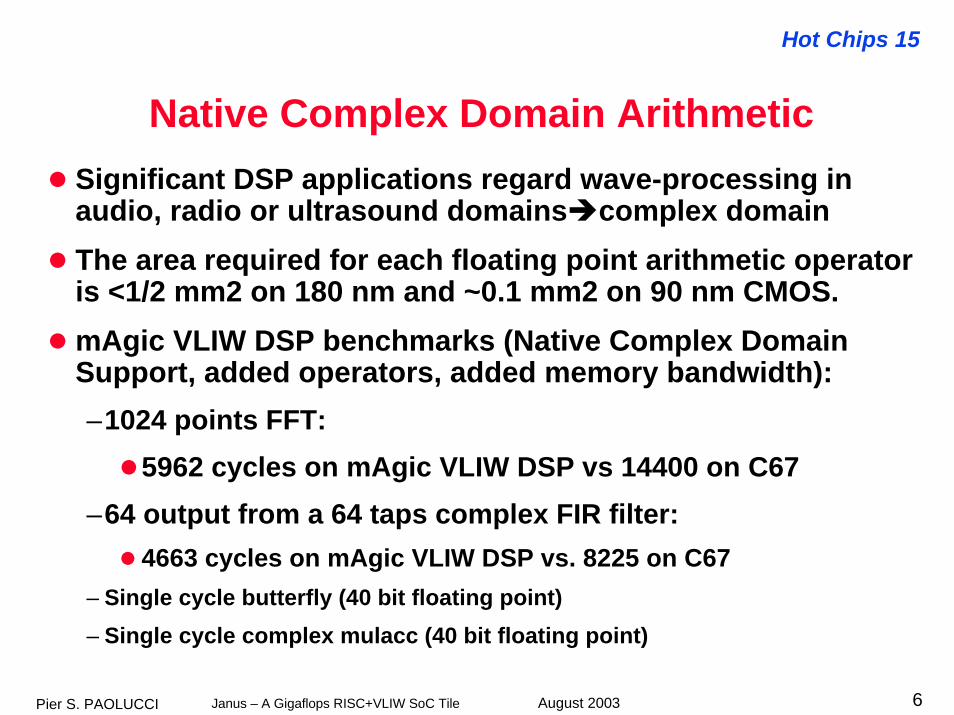
Native Complex Domain ArithmeticSignificant DSP applications regard wave-processing in audio, radio or ultrasound domains complex domainThe area required for each floating point arithmetic operator is <1/2 mm2 on 180 nm and ~0.1 mm2 on 90 nm CMOS. mAgic VLIW DSP benchmarks (Native Complex Domain Support, added operators, added memory bandwidth):–1024 points FFT:
5962 cycles on mAgic VLIW DSP vs 14400 on C67–64 output from a 64 taps complex FIR filter:
4663 cycles on mAgic VLIW DSP vs. 8225 on C67– Single cycle butterfly (40 bit floating point)– Single cycle complex mulacc (40 bit floating point)

Hot Chips 15
August 2003Janus – A Gigaflops RISC+VLIW SoC TilePier S. PAOLUCCI 7
mAgic™ Operator block• Operator
Block: 10 Float/Int Op per Cycle
• Complex Arithmetic support
• Vector 2 Arithmetic
• Butterfly Arithmetic
• Large (512)Multiport(8+8) Register File
Conv2Div2
Sh/Log2
Conv1Div1Sh/Log1
LEFT0 1 2 3
4 5 6 7
FP/I
*FP/I
*
RIGHT0 1 2 3
4 5 6 7
FP/I
*FP/I
*
FP/I
-FP/I
+
FP/I
- +FP/I
+ -
L Memory R Memory
L M
emor
y R M
emory
Mul1 Mul2 Mul4Mul3
Cadd1 Cadd2
Add1 Add2MinMax2
MinMax1

Hot Chips 15
August 2003Janus – A Gigaflops RISC+VLIW SoC TilePier S. PAOLUCCI 8
Automatic VLIW Scheduling
The designer writes in a serial fashion, and the assembler schedules optimized code that takes advantage of the DSPs Instruction Level Parallelism, accounting for data dependencies and latencies
IS SCHEDULED AS:
A=B+C; D=E*F;Q=Memory[I]
L=M+N;
G=A+D; P=Q*R
A SEQUENTIAL CODE LIKE:A=B+CD=E*FG=A+DL=M+NQ=Memory[I]P=Q*R

Hot Chips 15
August 2003Janus – A Gigaflops RISC+VLIW SoC TilePier S. PAOLUCCI 9
Multiple Address Generation Unit
S: 11 bits Start reg, vector absolute base address or circular buffer starting address
L: 11 bits Length reg, vector length
A: 11 bits Address reg, offset or abs base address
M: 7 bits Increment reg, increment
P: 9 bits Page reg, for internal memories pages addressing
Description Address out Modified A Assembly suffix
Just Use S+A A -
Modify & Use S+A+M A M
Use Modify & Update S+A A+M U
Modify Use & Update S+A+M A+M MU
Just Use S+A A -
Modify & Use S+A+M A M
Use Modify & Update S+A A+M U
Modify Use & Update S+A+M A+M MU
Just Use S+A A -
Modify & Use S+ (A+M)mod.L A M
Use Modify & Update S+A (A+M)mod.L U
Modify Use & Update S+ (A+M)mod.L (A+M)mod.L MU
Modular:
Offset: L=0
Linear: S=L=0
SLAMP fields and MAGU Addressing Modes

Hot Chips 15
August 2003Janus – A Gigaflops RISC+VLIW SoC TilePier S. PAOLUCCI 10
mAgic™ DSP Core interface with SoC Bus and External Memories
Slave memory mapped device on the controller’s system bus1.6 Mbit internal Program and Data Core Memories are memory mapped as wellXM DMA and SoC System Bus activities run in parallel with the core on dedicated Double Port Buffers
mAAR
Core Memories
mAgic DSP core
GlobalSequencer
mAgic Internal Resources Mapper (mIrm )
PM
P2P3
XM
Burst Service
Local Sequencer
RegisterFile
Operators
MAGU
PC
P 4
P1 P0
CSE Reg
mAgic System Mode Interface
ASB slave Wrapper
Registers
Hot Chips 15
August 2003Janus – A Gigaflops RISC+VLIW SoC TilePier S. PAOLUCCI 11
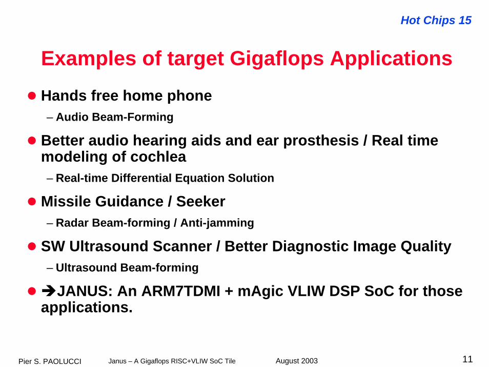
Examples of target Gigaflops Applications Hands free home phone– Audio Beam-Forming
Better audio hearing aids and ear prosthesis / Real time modeling of cochlea– Real-time Differential Equation Solution
Missile Guidance / Seeker– Radar Beam-forming / Anti-jamming
SW Ultrasound Scanner / Better Diagnostic Image Quality– Ultrasound Beam-forming
JANUS: An ARM7TDMI + mAgic VLIW DSP SoC for those applications.

Hot Chips 15
August 2003Janus – A Gigaflops RISC+VLIW SoC TilePier S. PAOLUCCI 12
Janus: a DUAL CORE VLIW DSP + RISC
mAgic VLIW FiPU DSP:1.5 GOPS @ 100 MHz(1.0 GFLOPS)
32 bit ARM7TDMI RISC
Set of SoC peripherals
1.9 Mbit SRAM on Board
352 BGA, 243 functional I/O
1.2 W worst case @ 100 MHz
Arm7TDMI32K ARM Mem ASB / APB Bridge
mAgic VLIW GigaFlopsDSP core
8Kx128 bitProgram
Mem
Shared Memory
Data Buffer 2 x 2k wordDouble Bank, Double Port
Amba ASBEB I
Data / Program Bus Mux
Program Bus Mux / Demux
Data Bus Mux / Demux
Data Mem2 x 6k x 40 bit Double BankDouble Port
SPI0
USART0
USART1
TIMER
Watchdog
PIO
PDC
ADDA
Clock Gen
IRQ Ctrl
Run Mode data pathsSystem Mode data pathsARM exclusive data paths
SPI1

Hot Chips 15
August 2003Janus – A Gigaflops RISC+VLIW SoC TilePier S. PAOLUCCI 13
Janus Floorplan & Technological Measurements
DSP Reg Files: 2 * 8 Ports * 256 Regs * 40 bit
mAgic VLIW floating point DSP SW Core: 15 op/cycle, 390 Kgate
DSP Progr SRAM: 2 * 1 Port * 8K * 64 bit
ARM7TDMI 32 BIT RISC CORE
RISC PERIPHERALS:135 Kgate
RISC SRAM: 4 * 1 Port * 8K * 8 bit
DSP Data SRAM: 8 * 2 Ports * 2K * 40 bit
Atmel 180 nm, five-level, Aluminum CMOS
Pad excluded, 39 mm2
Pad included, 55 mm2
243 functional IO
352 Ball Grid Array package
1.8 V (Core), 3.3 V (I/O)
<1.2 W (worst case) @ 100MHz
1.5 Gops, 1.0 Gigaflops
55 Kgate/mm2 effective density (10 mm2 for 550Kgate logic required for the software macros: VLIW DSP + Arm peripherals + testability stuff)

Hot Chips 15
August 2003Janus – A Gigaflops RISC+VLIW SoC TilePier S. PAOLUCCI 14
HW Tools: JANUS Test & Evaluation Board
CLKDIV
3.3V
RST
PLL
PIO
PIO
ARM DATA H SRAM128Kx8
ARM DATA L SRAM128Kx8
FLASHARM PRG512Kx16
SSRAMMAGICDATA L128Kx36
EXTCLK
MTM DIP SWITCH
SP
I-0
M-ICE
USART 0
RS232
Janus
PIO USARTsRST
XMAXMD[15:0]
CLKsCNTRLs
SPIsADDA
ARMD
PLL
ICEARMC
ARMA
XMD[55:40]
XMD[31:16]
XMD[71:56]
XMD[39:32]XMD[79:72]
SP
I-1
SSRAMMAGICDATA H128Kx36
SSRAMMAGICDATA E128Kx36
USART 1
USBCNTRLU
SB
D-9 RS232 D-9 RS232
RS232RS232
3.3-1.8
EX
T P
SU
uPR
CO
DE
C
LEDBUFF
CO
DE
C(o
pt)
CO
DE
C(o
pt)
CO
DE
C(o
pt)
LINEIN
LINEOUT
LINEIN
(opt)
LINEOUT(opt)
LINEIN
(opt)
LINEOUT(opt)
LINEIN
(opt)
LINEOUT(opt)
CLKDIV
25 MHz
MTM Works @ 100MHz andProvides the following resources:
– Memories for mAgic and ARM
– Stereo Audio CODECs (up to 4)– Serial I/O:
1 USB 2.0 Full Speed (12 Mbps)2 RS232/LVTTL a/sync serial lines2 SPI serial I/O lines1 ÷ 4 audio codecs
– IO connectors (USART, SPI, PIO, AUDIO)– Configuration DIP SWITCH– Status 7-segment Display– JTAG ARM M-ICE connector
– Size: 5 x 5 inch2 (12.7x12.7 cm2)

Hot Chips 15
August 2003Janus – A Gigaflops RISC+VLIW SoC TilePier S. PAOLUCCI 15
Development EffortOur SIMD/VLIW mAgic DSP architecture is largely based on the know-how acquired by some of the authors thanks to their participation to three generations of the Massively Parallel Processing experiment APE, conducted since 1983 by INFN (Istituto Nazionale di Fisica Nucleare). The design and development of custom VLIW processors, hardware and system software for those machines accounted for more than 300 Person Years.
From that background, the development and validation of mAgic VLIW DSP and the essential system software required approximately 65 Person Years.
The integration and validation at Janus level with the ARM core and the set of pre-validated ARM peripherals, plus physical design and validation board activities should required approximately 10 Person Years.

Hot Chips 15
August 2003Janus – A Gigaflops RISC+VLIW SoC TilePier S. PAOLUCCI 16
A Differentiation Era beyond the Single Processor Barrier
Log
(Sys
tem
Com
plex
ity)
Time
Massive Parallel Computers
SuperScalar
32 bit Float Multiplier
Resources available on a single chip
1980
Single Processor Barrier
1990 2000 2010
Risc Forced Convergence
Era
Multi Core DifferentiationEra
Power density, overhead logic and interconnect delays for monolithic high clock speed processor design are approaching embarrassing figures according to ITRS. The human brain has got a processing power >> 106 times than DSP processors of 2003, yet runs at <<100 Hz, ~10W. A precious Hint for adoption of moderate clock speed, better memory architectures and parallelism management to exploit higher silicon densities provided by DSM technologies?

Hot Chips 15
August 2003Janus – A Gigaflops RISC+VLIW SoC TilePier S. PAOLUCCI 17
Dimensional Analysis for Deep Sub-Micron Processor design with ASIC methodology
A possible concern regarding synthesizable cores for next decadeSoCs: maximum frequency dominated by wire delays, not by gate
propagation
our simple dimensional analysis suggests that:
– adequate ILP + multiple tiles, lower clock speed, lower pipelining, shorter wire lengths simpler design closure
– floating point relatively un-expensive Balancing Memory area vs. Operating area
– DSP treatment of wave phenomena useful ILP >= 15 native complex domain support

Hot Chips 15
August 2003Janus – A Gigaflops RISC+VLIW SoC TilePier S. PAOLUCCI 18
Multiple Tile SoC: Tiles for Short Wires
External Memories Interface
RISC
Mem
DSP Prog
MemD
SP Data
mem
Reg File
VLIW
DSP
RISC
Y+ Communication Interface
Y- Communication Interface
X-Com
munication
X+ Com
munication
RISC
Mem
DSP Prog
Mem
DSP D
ata
mem
Reg File
VLIW
DSP
RISC
Y+ Communication Interface
Y- Communication Interface
X-Com
munication
X+ Com
munication
Y- Communication Interface Y- Communication Interface

Hot Chips 15
August 2003Janus – A Gigaflops RISC+VLIW SoC TilePier S. PAOLUCCI 19
ILP * frequency vs. Wire Delayr and c := technological resistance and capacitance per wire unit length (e.g. 180 nm rc = 58 ps/mm2, 90 nm rc = 160ps/mm2)L := processor’s tile size; 2L:=worst Manhattan path lengthg:= gate density (e.g. 180 nm g=55Kgate/mm2; 90 nm g=200Kgate/mm2)o:= arithmetic operator cost (e.g. 7Kgate 24 bit floating point, 25Kgate 40 bit)
)4(rcog66.ILP*wfwG
)3(2LogILP
)2(rc38.1pt2TLL2
)1(2)L2(rc38.
1RC38.
1wf0f
≤=
≤
==
≤=≤ logic delay f0, wire delay fw. f0<< fwindicates designs far away from interconnect troubles
LT repeater insertion critical length ~ 4.4mm ~ 419 ps on 180 nm
L2 areas support VLIW ILP determined by gate density over operator cost
peak power for a VLIW area below critical area (NOTE the interesting independency on size and ILP)

Hot Chips 15
August 2003Janus – A Gigaflops RISC+VLIW SoC TilePier S. PAOLUCCI 20
Dimentional HintsEquation (4) Gw =fw * ILP <= .66 g/rco, provides suggestions:
At one extreme, it states the obvious. You should divide a die too large into N smaller tiles.At intermediate scale, it suggests to insert at least the number of operators that can be reached by non repeated wires. In fact a lower frequency reduces the number of local pipelines, permits the adoption of a classical ASIC RTL methodology and simplifies the adoption of lower Vdd.A lower bound for the ILP is imposed by:– adequate program and data memory inside each tile– maintain a higher granularity to avoid classical massive parallel processing
inefficiencies– balance memory vs processing resources

Hot Chips 15
August 2003Janus – A Gigaflops RISC+VLIW SoC TilePier S. PAOLUCCI 21
mAgic VLIW Arith Oper Gate Count#Units Combina
torialNon Comb.
Total Grand Total
4 40 bit Float Adder 10900 8400 19300 77200
4 40 bit Float and 32 bit Int Mult
24100 2700 26800 107200
4 32 bit Int Adder 900 1600 2500 10000
2 Float Div & Sqrt Seed 3300 700 4000 8000
2 40 bit Shift & Logic Unit 6600 800 7400 14800
2 Float<->Int Converter 4500 400 4900 9800
1 Decoder 1200 1700 2900 2900
Total VLIW Arithmetic Operators
251300
SUPPORT FOR NATIVE COMPLEX DOMAIN 40-bit FLOATING POINT ARITHMETIC <= 1.5 mm2 on 90 nm CMOS

Hot Chips 15
August 2003Janus – A Gigaflops RISC+VLIW SoC TilePier S. PAOLUCCI 22
mAgic VLIW Floating Point DSP Gate CountCombinatorial
Non Comb.
Total
VLIW Arithmetic & Logic Operators 186800 64500 251300VLIW Multiple Address Generation Unit 18900 13100 32000VLIW Flow Controller 8300 18000 26300VLIW DMA + Global Status Controller 4600 11300 15900VLIW Program Decompression Engine 7600 10500 18100VLIW Local Memory Mux Logic & Bist 18700 13800 32500VLIW<->RISC Memory Mapping Interface 1300 6800 8100VLIW DSP ENGINE TOTAL GATE COUNT 250400 141400 391800
payload for mAgic VLIW core >= 70% grows to 90% considering processor + memory tiles
equations (3) and (4) are reasonable approximations

Hot Chips 15
August 2003Janus – A Gigaflops RISC+VLIW SoC TilePier S. PAOLUCCI 23
Dimensional Analysis results
On 180 nm Atmel technology, the gate delay for a 25 Kgate 40-bit floating point operator with two pipeline stages is 8 ns. Therefore f0<< fw for the full VLIW core with ILP = 15. Complete RISC+VLIW logic area ~ 10 mm2, 550 Kgates
On 90 nm copper CMOS, f0 / fw ~ 1 / 6for the 250 Kgate complex domain data path with 10 floating point operators. A pipeline stage will be required on core<->memory busses.
8 Gigaflops, 4 Janus tiles SOC feasible with ASIC methodology on 90 nm technology with classical RTL synchronous design. Insertion of repeaters and promotion of global wires on thicker layers helps, but is not yet mandatory.

Hot Chips 15
August 2003Janus – A Gigaflops RISC+VLIW SoC TilePier S. PAOLUCCI 24
SummarymAgic VLIW DSP: a synthesizable complex domain floating point core: 1.0 Gigaflops @ 100 MHz, 180 nm CMOSJanus: a 180 nm RISC+floating point VLIW platform for Gigaflops SoC applicationsA Dimensional Analysis based on the technological parameter g/rcoprovides an interconnect bound to the processing power of simplesynthesizable RTL designs on DSM techologies with ASIC methodologyWe will follow a simple roadmap for SoC integration of multiple gigaflops on 90 nm using:– Tiles for Short Wires– Appropriate VLIW parallelism– Moderate Clock Speed– This methodology keeps the cost down to a few tens of designers and M$.


![Code Generation Schemes for Modulo Scheduled DO-Loops and ... · [9]. Modulo scheduling is applicable to RISC, CISC, superscalar, superpipelined, and VLIW processors, and is useful](https://img.dokumen.tips/doc/110x75/5f2f57bdb3e99404196933c2/code-generation-schemes-for-modulo-scheduled-do-loops-and-9-modulo-scheduling.jpg)