Embed Size (px)
Citation preview

Standard Power
Data Sheet
Rev 1.0, 2015-04-28
ITS42k5D-LD-FDual Channel High-Side PMOS Power Switch with Integrated Freewheeling Diodes
PG-TSON-10
Type Package MarkingITS42k5D-LD-F PG-TSON-10 I2k5DF
Data Sheet 2 Rev 1.0, 2015-04-28
Dual Channel High-Side PMOS Power Switch with Integrated Freewheeling Diodes
ITS42k5D-LD-F
1 Overview
Features• Two channel power PMOS high-side switch• Integrated freewheeling diode • Output current capability: up to 250mA per channel• Wide operating voltage range: 4.5V to 42V• Very low quiescent current in OFF state• High current limit accuracy• 3.3V and 5V compatible logic inputs• Optimized EMC behavior• Overload, short circuit, open load and overtemperature diagnosis• ESD, short circuit, safe operation area and overtemperature protection• Undervoltage lockout (UVLO)• Green and robust product (RoHS compliant)
DescriptionThe ITS42k5D-LD-F, which is available in a very small leadless PG-TSON-10 package, is a 2.5Ω dual channelhigh-side PMOS power switch with integrated freewheeling diodes including protection and diagnostic functions.The ITS42k5D-LD-F has two diagnostic status output pins, one for each channel.The diagnosis can be read out from two separate open drain outputs in order to indicate overload, short circuit,open load and overtemperature conditions. The device controls the respective channel one or two by the twoseparate input pins i.e. IN1 and IN2. When both inputs are low the device is in OFF condition. Each channel of thedevice is able to drive loads up to 250mA.
Application rangeThe ITS42k5D-LD-F is capable of switching resistive, capacitive and inductive loads (e.g. sensor units, LEDs,relays, valves) in harsh industrial environments. An integrated freewheeling diode enables driving of inductiveloads. The ITS42k5D-LD-F is suitable for switching small loads such as sensors. For sensor supplies please referto Infineon’s industrial linear voltage regulator products. The qualification of this product is based on JEDEC JESD47 and may reference existing qualification results ofsimilar products. Such referencing is justified by the structural similarity of the products. The product is not qualifiedand manufactured according to the requirements of Infineon Technologies with regard to automotive and/ortransportation applications.

Data Sheet 3 Rev 1.0, 2015-04-28
ITS42k5D-LD-F
Overview
Infineon Technologies administrates a comprehensive quality management system according to the latest versionof the ISO9001 and ISO/TS 16949. The most updated certificates of the aforesaid ISO9001 and ISOTS 16949 are available on the InfineonTechnologies web page http://www.infineon.com/cms/en/product/technology/quality/

Data Sheet 4 Rev 1.0, 2015-04-28
ITS42k5D-LD-F
Pin Configuration
2 Pin Configuration
2.1 Pin Assignment
Figure 1 Pin configuration top view, PG-TSON-10
2.2 Pin Definitions and Functions
Table 1 Pin DefinitionPin Symbol Function1 IN1 INPUT 1; Control Input for Channel 1, Active High2 ST1 STATUS 1; Status Flag for Channel 1; Open Drain Output3 SGND SIGNAL GND; connect to all GNDs and to exposed GND pad4 ST2 STATUS 2; Status Flag for Channel 2; Open Drain Output5 IN2 INPUT 2; Control Input for Channel 2; Active High6 GND2 Ground Channel 2; Connect to all GNDs and to exposed GND pad7 OUT2 OUTPUT 2; drain of the power-PMOS Channel 2; power freewheeling diode to
GND8 VS Supply Voltage; block to GND with a capacitor near the IC9 OUT1 OUTPUT 1; drain of the power-PMOS Channel 1; power freewheeling diode to
GND10 GND1 Ground Channel 1; Connect to all GNDs and to exposed GND padExposed pad – Connect externally to all GNDs i.e. GND1, GND2 and SGND
1
2
3
4
5 6
7
8
9
10IN1
ST1
SGND
ST2
IN2
GND1
OUT2
GND2
VS
OUT1
PG-TSON-10

Data Sheet 5 Rev 1.0, 2015-04-28
ITS42k5D-LD-F
Block Diagram
3 Block Diagram
3.1 ITS42k5D-LD-F in the PG-TSON-10 package
Figure 2 Block diagram ITS42k5D-LD-F
Diagnosis
Biasing
SuperVision
VS
8
6 79 310
4
5
StandyBy
Control
InputInterface
ITS42k5D-LD-F
IN2
ST2Diagnosis2
1
StandyBy
Control
InputInterfaceIN1
ST1
Driver
Protector
OFF
Driver
Protector
OFF

Data Sheet 6 Rev 1.0, 2015-04-28
ITS42k5D-LD-F
Functional Description
4 Functional Description
4.1 Input CircuitThe two inputs i.e. IN1 and IN2 control the outputs of channel 1 and channel 2 respectively.When both inputs IN1 and IN2 are low the device is switched OFF. In OFF state, the current consumption of thedevice is very low. For more details on current consumption in ON and OFF states please refer to electricalcharacteristics. The logic input levels are compatible with 3.3V and 5V microcontrollers. To avoid switching noiseall inputs have hysteresis. Logic level definitions are shown in Figure 3
Figure 3 Function and Thresholds of the inputs IN1 and IN2
The input pins are optimized in terms of ESD protection, withstanding overvoltage scenarios like surge pulses.Overvoltage transient levels higher than the maximum ratings of 45V must be avoided.Note: Exposure to absolute maximum rating conditions for extended periods may affect device reliability.
Integrated protection functions are designed to prevent IC destruction under fault conditions described in the data sheet. Fault conditions are considered as “outside” the normal operating range. Protection functions are neither designed for continuous nor repetitive operation.
4.2 PowerstageThe two outputs are designed as high-side switches with integrated freewheeling diodes from OUT to GND. Thehigh side switch is a power P-channel MOSFET. The integrated freewheeling diodes enable the device to switchinductive loads on each channel.A built-in high accuracy current limiter ensures that the Power P-channel MOSFET is protected against overloadwhen driving heavy capacitive loads.Figure 4 shows the output voltage VOUT1 and VOUT2 controlled by the input interfaces IN1, IN2
VINL
t
VIN
VINH
OFFOFF ON
VINHY
Powerstage

Data Sheet 7 Rev 1.0, 2015-04-28
ITS42k5D-LD-F
Functional Description
Figure 4 Input / output timings when switching a resistive load.
4.3 Protection Functions
Note: Exposure to absolute maximum rating conditions for extended periods may affect device reliability. Integrated protection functions are designed to prevent IC destruction under fault conditions described in the data sheet. Fault conditions are considered as “outside” the normal operating range. Protection functions are neither designed for continuous nor repetitive operation.
4.3.1 Short Circuit ProtectionShort circuit is a special case of overload. The device is protected within the supply voltage range from VS = 4.5V to 42 V. If the device stays in short circuit condition for a longer time the integrated temperature protection willswitch the device OFF (both channels OFF). For details please look at chapter “Overtemperature Protection”.
4.3.2 Protection by Overtemperature ShutdownThis circuit monitors the junction temperature Tj. When the device is ON, the junction temperature Tj increasesproportional to the power loss. The temperature protector is equipped with two temperature sensors, one for eachone of the powerstages. When the thermal shutdown trip point TSDOFF is reached, the in-built protector switchesOFF the respective channel. This overtemperature shutdown is reported via diagnosis to the respective status flagi.e. either ST1 and ST2. The output remains OFF until the junction is cooled down to the thermal shutdown releasepoint TSDON. If the overload condition remains the device will toggle between both junction temperature values. Itis not recommended for the device to stay in an overload condition as this will degrade its lifetime.
VOUT
VIN
10%
90%
tON tOFF
SR ON =(dV/dt)ON
tf
VINH
VINL
t
100%tr
SR OFF =(dV/dt)OFF
t

Data Sheet 8 Rev 1.0, 2015-04-28
ITS42k5D-LD-F
Functional Description
4.4 DiagnosisFor diagnostic purposes the device provides two digital output pins ST1 and ST2 in order to indicate faultconditions.The status flag ST1 indicates the status of channel 1 and flag ST2 indicates the status of channel 2.Each status output (ST1, ST2) of the ITS42k5D-LD-F is a high voltage open drain output.In “normal” operation mode the NMOS open drain transistors are switched OFF. The following truth table (Table 2)defines the status output of the device under various conditions.
4.5 Undervoltage LockoutIn order to avoid an application malfunction caused by an undervoltage condition at the load (e.g. a relay can notkeep the contact closed properly) an undervoltage lockout (UVLO) supervises the supply voltage Vs.The UVLO circuit switches the power stages off if the supply voltage is below the functional operating voltagerange
Figure 5 Under Voltage Lockout (UVLO) function and thresholds
Table 2 Truth table of diagnosis featureDevice Operation IN1 IN2 ST1 ST2 CommentNormal Operation H H H H –Overload H H L L Respective flag is low; latchedShort Circuit to GND H H L L Respective flag is low; latchedOvertemperature H H L L Respective flag is low; latchedOvertemperature L L H H Device in OFF mode; no internal heat sourceOpen Load H H L L Respective flag is low
VUVOFF
t
VS
VUVON
OFFOFF ON
VUVHY
Powerstage
VOUT1,2

Data Sheet 9 Rev 1.0, 2015-04-28
ITS42k5D-LD-F
Functional Description
4.6 Protection Behavior
Figure 6 Protection mechanism of the ITS42k5D-LD-F
Device turn ON in an open load: Open load condition during on state :
t t
OFFOFF
VOUT
t
t
0
IOUTL
0
Open load status flag delay while ON
VOUT
t
VIN
Lt
0
IOUTL
0ILOL
L
HVST
t
HVIN
L
H
L
HVST
ttdOLoff tdOLONf
ON
Open load status flag delay from OFF
ILOL
ON in OL
tdOLONr
OFFONON in OL
IHOL

Data Sheet 10 Rev 1.0, 2015-04-28
ITS42k5D-LD-F
Functional Description
Figure 7 Protection behavior of the ITS42k5D-LD-F
Overtemperature concept: Overtemperature behavior:
OvertemperatureTogglingNormal
Waveforms turn on into a short circuit: Waveforms short circuit during on state:
t t
OFFOFF Overload OUT shorted to GNDOFF Normaloperation
ON
TSDOFF
TSDHY
VOUT
t
t
0
IOUTL
0tSCOFF
Shut down by overtemperature andrestart by cooling (toggling)
Shut down by overtemperature andrestart by cooling (toggling)
VOUT
t
VIN
Lt
0
IOUTL
0
t
OFFOFF ON ON
VOUT
t
t
0
TJ
t
TSDOFFTSDHY
OFF
TJOFF
TSDON
cooling down
heating up
DeviceStatus
L
HVST
t
HVIN
L
H
L
HVST
ttdP
VIN
L
H
L
HVST
t
IOUTL maxControlled by the current limit circuit
IOUTL maxControlled by the current limit circuit
TSDON

Data Sheet 11 Rev 1.0, 2015-04-28
ITS42k5D-LD-F
Functional Description
4.7 Application Waveforms
Figure 8 Protection behavior of the ITS42k5D-LD-F
General Input Output waveforms:
VS
t
VIN
t
0
IOUTL
t0
OFFOFF ON
VDS
VOUT
90%
0
+VS
10%
tOFF
VIN
t
IOUTL
t0
tON
SRON
SROFF
t
Waveforms switching a resistive load:
OFFOFF ON ON
Waveforms switching a capacitive load: Waveforms switching an inducitive load :
VOUT
t
VIN
t
0
IOUTL
t0
~ VSVOUT
t
VIN
t
0
IOUTL
t0
~ VS
tVOUT
VF
OFFOFF ON ON OFFOFF ON ON
L
H
L
H
L
H
L
H

Data Sheet 12 Rev 1.0, 2015-04-28
ITS42k5D-LD-F
General Product Characteristics
5 General Product Characteristics
5.1 Absolute Maximum Ratings
Note: Exposure to absolute maximum rating conditions for extended periods may affect device reliability. Integrated protection functions are designed to prevent IC destruction under fault conditions described in the data sheet. Fault conditions are considered as “outside” the normal operating range. Protection functions are neither designed for continuous nor repetitive operation.
Table 3 Absolute maximum ratings1)Tj = -40°C to +125° unless otherwise specified; all voltages with respect to ground unless otherwise specified
1) Not subject to production test, specified by design
Parameter Symbol Values Unit Note / Test Condition
NumberMin. Typ. Max.
Supply voltage VSVoltage VS -0.3 – 45 V – 5.1.1Current IS -10 – – mA Internally limited 5.1.2Input IN1 and IN2Input Voltage VIN1,2 -0.3 – 45 V – 5.1.3Current I IN1,2 – – – mA Internally limited 5.1.4Output STVoltage VST1,2 -0.3 – 45 V – 5.1.5Current I ST1,2 – – 5 mA – 5.1.6Ground GND1, GND2, SGNDCurrent IGND1, 2 – – 600 mA Internally limited 5.1.7Current ISGND – – 10 mA Internally limited 5.1.8Output stage OUT1, OUT2Voltage VOUT1, 2 – – VS+ 0.3 V Internally limited 5.1.9TemperaturesJunction Temperature Tj -40 – 150 °C – 5.1.11Storage Temperature Tstg -55 – 150 °C – 5.1.12Power DissipationPower dissipation Ptot – 0.66 – W PCB2) is vertical
without blown air
2) See Thermal Resistance Footnote 2)
5.1.13
ESD SusceptibilityESD susceptibility (all pins) VESD -2 – 2 kV HBM3)
3) ESD susceptibility, HBM according to ANSI/ESDA/JEDEC JS-001 (1.5kΩ, 100pF)
5.1.14ESD susceptibility OUT pins vs. GND pin
VESD -2 – 2 kV 5.1.15
ESD susceptibility (all pins) VESD -1 – 1 kV CDM4)
4) ESD susceptibility, Charged Device Model “CDM” JEDEC JESD22-C101
5.1.15

Data Sheet 13 Rev 1.0, 2015-04-28
ITS42k5D-LD-F
General Product Characteristics
5.2 Functional Range
Note: Within the functional range the IC operates as described in the circuit description. The electrical characteristics are specified within the conditions given in the related electrical characteristics table.
5.3 Thermal ResistanceThis thermal data was generated in accordance with JEDEC JESD51 standards.More information on www.jedec.org
Table 4 Functional Range1)
1) Not subject to production test, specified by design
Parameter Symbol Values Unit Note / Test Condition
NumberMin. Typ. Max.
Nominal Operating Voltage VS VUVON – 42 V VS increasing 5.2.1Nominal Operating Voltage VS VUVOFF – 42 V VS decreasing 5.2.2Nominal Operating Voltage VIN1,2 -0.3 – 7 V – 5.2.3Nominal Operating Voltage VST1,2 -0.3 – 7 V – 5.2.4Junction Temperature Tj -40 – 125 °C – 5.2.5
Table 5 Thermal Resistance1)
1) Not subject to production test, specified by design
Parameter Symbol Values Unit Note / Test Condition
NumberMin. Typ. Max.
PG-TSON-10 Junction to Case, exposed pad Rthjc – 12 – K/W 5.3.1Junction to ambient RthJA_1s0p – 140 – K/W 2)
2) Specified RthJA value is according to Jedec JESD51-3 at natural convection on FR4 1s0p board, footprint; the Product (Chip+Package) was simulated on a 76.2 x 114.3 x 1.5 mm board with 1x 70µm Cu.
5.3.2Junction to ambient RthJA_1s0p_300mm – 70 – K/W 3)
3) Specified RthJA value is according to Jedec JESD51-3 at natural convection on FR4 1s0p board, Cu, 300mm2; the Product (Chip+Package) was simulated on a 76.2 x 114.3 x 1.5 mm board with 1x 70µm Cu.
5.3.3Junction to ambient RthJA_1s0p_600mm – 60 – K/W 4)
4) Specified RthJA value is according to Jedec JESD51-3 at natural convection on FR4 1s0p board, 600mm2; the Product (Chip+Package) was simulated on a 76.2 x 114.3 x 1.5 mm board with 1x 70µm Cu.
5.3.4Junction to ambient RthJA_2s2p – 67 – K/W 5)
5) Specified RthJA value is according to Jedec JESD51-2,-5,-7 at natural convection on FR4 2s2p board; the Product (Chip+Package) was simulated on a 76.2 x 114.3 x 1.5 mm board with 2 inner copper layers (2 x 70µm Cu, 2 x 35µm Cu).
5.3.5Junction to ambient RthJA_2s2pvia – 55 – K/W 6)
6) Specified RthJA value is according to Jedec JESD51-2,-5,-7 at natural convection on FR4 2s2p board with two thermal vias; the Product (Chip+Package) was simulated on a 76.2 x 114.3 x 1.5 mm board with 2 inner copper layers (2 x 70µm Cu, 2 x 35µm Cu. The diameter of the two vias are equal 0.3mm and have a plating of 25um with a copper heatsink area of 3mm x 2mm). JEDEC51-7: The two plated-through hole vias should have a solder land of no less than 1.25 mm diameter with a drill hole of no less than 0.85 mm diameter.
5.3.6

Data Sheet 14 Rev 1.0, 2015-04-28
ITS42k5D-LD-F
Electrical Characteristics
6 Electrical Characteristics
Table 6 VS = 4.5 V to 42 V ; Tj = -40°C to +125°, all voltages with respect to ground, currents flowing into the device unless otherwise specified ; typical values are given at VS = 13.5 V, Tj = 25°C
Parameter Symbol Values Unit Note / Test Condition
NumberMin. Typ. Max.
InputON Threshold VINH1, 2 2 – – V – 6.1.1OFF Threshold VINL1,2 – – 0.8 V – 6.1.2Input Hysteresis VINHY1,2 0.1 0.4 – V VINHY= VINH - VINL 6.1.3Input Current - ON state IINON1, 2 10 25 50 µA VIN = 5V 6.1.4Input Pull Down Resistor;IN1,2 to SGND
RIN1,2 100 200 300 kΩ – 6.1.5
PowerstagePMOS ON Resistance RDSON1,2 – 2.5 8 Ω IOUT1, 2 = 250mA 6.1.6PMOS ON Resistance RDSON1,2 – 2.5 4 Ω IOUT1, 2 = 250mA;
Tj = 25°C;6.1.7
Freewheeling DiodeForward Voltage
VF1,2 – – 1.5 V IF1, 2 = 250mA 6.1.8
Freewheeling DiodeForward Voltage
VF1,2 – 1.0 1.2 V IF1, 2 = 250mATj = 25°C;
6.1.9
Output Leakage Current (PMOS) IOUTLK1,2 – – 2 µA VIN1 = VIN2 = 0V;VOUT1, 2 = 0V; Tj = -40°C to 105°C
6.1.10
Output Leakage Current (Diode) IOUTLK1,2 -2 – – µA VIN1 = VIN2 = 0VVOUT1, 2 = VS;Tj = -40°C to 105°C
6.1.11
Turn ON Time (to 90% of VOUT) tON1,2 6 12 25 µs VS=13.5V;RL1, 2 = 51Ω
6.1.12
Turn OFF Time (to 10% of VOUT) tOFF1,2 8 16 30 µs VS=13.5V;RL1, 2 = 51Ω
6.1.13
Rise Time (from 10% to 90% of VOUT)
tr1,2 3 6 15 µs VS=13.5V;RL1, 2 = 51Ω
6.1.14
Fall Time (from 90% to 10% of VOUT)
tf1,2 3 6 15 µs VS=13.5V;RL1, 2 = 51Ω
6.1.15
Slew Rate ON = dV/dt (10% to 90% of VOUT)
SRON1,2 0.7 1.7 3.5 V/µs VS=13.5V;RL1, 2 = 51Ω
6.1.16
Slew Rate OFF = - dV/dt (10% to 90% of VOUT)
SROFF1,2 0.7 1.7 3.5 V/µs VS=13.5V;RL1, 2 = 51Ω
6.1.17
Current consumptionQuiescent Current in OFF Mode ISOFF – – 1 µA Tj = -40°C to 85°C;
VIN1 = VIN2 = 0V;RL1, 2 = 51Ω
6.1.18

Data Sheet 15 Rev 1.0, 2015-04-28
ITS42k5D-LD-F
Electrical Characteristics
Quiescent Current in OFF Mode ISOFF – – 5 µA Tj = -40°C to 105°C;VIN1 = VIN2 = 0V;RL1, 2 = 51Ω
6.1.19
Current Consumption in ON Mode without load
ISON – 3 5 mA VIN1,= VIN2 = 5V;OUT1, 2 open
6.1.20
Current Consumption in ON Mode without load
ISON – 3 4 mA VIN1,= VIN2 = 5V;Tj = 25°C; OUT1, 2 open
6.1.21
Current Consumption in ON Mode; with resistive nominal loadsISON = IS - IOUT1 - IOUT2
ISON – 3 5 mA VIN1,= VIN2 = 5V;RL1 = RL2 = 51Ω;VS = 13.5 V
6.1.22
Overload Protection Current Limit1)
Output Current Limitation IOUTL1, 2 250 400 600 mA 4.5V < VDS1,2 < 20V 6.1.23Output Current Limitation IOUTL1, 2 200 300 – mA VDS1,2 = 30V 6.1.24Output Current Limitation IOUTL1, 2 50 150 – mA VDS1,2 = 42V 6.1.25Status flag time after positive input slope2)
tdP1,2 – 60 – µs – 6.1.26
Overtemperature Protection1)
Thermal Shutdown Trip Point TSDOFF 150 175 200 °C – 6.1.27Thermal Shutdown Release Point TSDON 125 150 175 °C – 6.1.28Thermal Shutdown Hysteresis TSDHY – 25 – °C – 6.1.29Open Load DiagnosisOpen Load Detection Threshold in ON state; ST going from high to low
ILOL 0.2 3.5 8 mA VS = 13.5VTj = 25°C
6.1.30
Open Load Detection Threshold in ON state; ST going from low to high
IHOL 1 5 9.5 mA VS = 13.5VTj = 25°C
6.1.31
Open Load Detection Threshold Hysteresis in ON state
ILOLHYS 0.2 1.5 – mA VS = 13.5VTj = 25°C
6.1.32
Status flag time after positive input slope while in Open Load
tdOLOFF1,2 – 18 – µs VS = 13.5VTj = 25°C
6.1.33
Status flag time while ON after Open Load event
tdOLONf1,2 – 42 – µs VS = 13.5VTj = 25°C
6.1.34
Status flag time while ON going out of Open Load
tdOLONr1,2 – 10 – µs VS = 13.5VTj = 25°C
6.1.35
Status FlagStatus Drop Voltage when L VSTL1,2 – 200 400 mV IST1,2 = 3mA 6.1.36Status Leakage Current when H ISTLK1,2 – – 10 µA VST1,2 = 7V 6.1.37Undervoltage LockoutUV Switch ON Voltage VUVON 3.75 4.25 4.5 V VS increasing 6.1.38UV Switch OFF Voltage VUVOFF 3.25 3.75 4.25 V VS decreasing 6.1.39UV ON/OFF Hysteresis VUVHY 0.2 0.5 – V VUVON - VUVOFF 6.1.40
Table 6 VS = 4.5 V to 42 V ; Tj = -40°C to +125°, all voltages with respect to ground, currents flowing into the device unless otherwise specified ; typical values are given at VS = 13.5 V, Tj = 25°C
Parameter Symbol Values Unit Note / Test Condition
NumberMin. Typ. Max.

Data Sheet 16 Rev 1.0, 2015-04-28
ITS42k5D-LD-F
Electrical Characteristics
1) Please refer to chapter “Protection Functions” on Page 72) No delay time after overtemparature switch off and short circuit in on-state.

Data Sheet 17 Rev 1.0, 2015-04-28
ITS42k5D-LD-F
Typical Performance Graphs
7 Typical Performance Graphs
Typical Performance Characteristics
On-Resistance RDSONversusJunction Temperature Tj
On-Resistance RDSONversusSupply Voltage VS
Switch ON Time tON versusJunction Temperature Tj
Switch OFF Time tOFFversusJunction Temperature Tj
0 50 1000
0.5
1
1.5
2
2.5
3
3.5
4
Tj [°C]
RD
SO
N [Ω
]
VS = 13.5V IOUT = 50 mA
IOUT = 150 mA
IOUT = 250 mA
5 10 15 20 25 30 35 400
0.5
1
1.5
2
2.5
3
3.5
4
VS [V]
RD
SO
N [Ω
]
IOUT = 250mA
Tj = −40 °C
Tj = 25 °C
Tj = 125 °C
0 50 1000
5
10
15
20
25
Tj [°C]
t ON [µ
s]
IOUT = 50 mA
IOUT = 150 mA
IOUT = 250 mA
0 50 1000
5
10
15
20
25
Tj [°C]
t OF
F [µ
s]
IOUT = 50 mA
IOUT = 150 mA
IOUT = 250 mA
Data Sheet 18 Rev 1.0, 2015-04-28
ITS42k5D-LD-F
Typical Performance Graphs
Typical Performance Characteristics
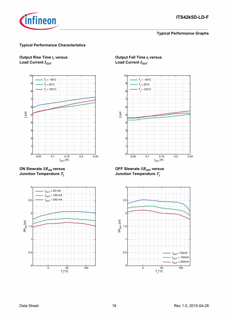
Output Rise Time tr versus Load Current IOUT
Output Fall Time tf versus Load Current IOUT
ON Slewrate SRON versusJunction Temperature Tj
OFF Slewrate SROFF versusJunction Temperature Tj
0.05 0.1 0.15 0.2 0.250
1
2
3
4
5
6
7
8
9
10
IOUT [A]
t r [µs]
Tj = −40°C
Tj = 25°C
Tj = 125°C
0.05 0.1 0.15 0.2 0.250
1
2
3
4
5
6
7
8
9
10
IOUT [A]
t f [µs]
Tj = −40°C
Tj = 25°C
Tj = 125°C
0 50 1000
0.5
1
1.5
2
2.5
3
Tj [°C]
SR
ON [µ
s]
IOUT = 50 mA
IOUT = 150 mA
IOUT = 250 mA
0 50 1000
0.5
1
1.5
2
2.5
3
Tj [°C]
SR
OF
F [µ
s]
IOUT = 50mA
IOUT = 150mA
IOUT = 250mA

Data Sheet 19 Rev 1.0, 2015-04-28
ITS42k5D-LD-F
Typical Performance Graphs
Typical Performance Characteristics
ON Supply Current ISON versus Junction Temperature Tj
ON Supply Current ISON versus Supply Voltage VS
Quiescent Current in OFF mode ISOFFversus Junction Temperature Tj
Quiescent Current in OFF mode ISOFFversus Supply Voltage VS
0 50 1000
1
2
3
4
5
6
7
8
9
10
Tj [°C]
I SO
N [m
A]
VS = 4.5 V
VS = 13.5 V
VS = 24 V
VS = 42 V
5 10 15 20 25 30 35 401
2
3
4
5
6
7
8
9
10
VS [V]
I SO
N [m
A]
Tj = −40°C
Tj = 0°C
Tj = 50°C
Tj = 125°C
0 50 1000
0.05
0.1
0.15
0.2
0.25
0.3
0.35
0.4
0.45
0.5
Tj [°C]
I SO
FF [µ
A]
VS = 4.5 V
VS = 13.5 V
VS = 24 V
VS = 42 V
5 10 15 20 25 30 35 400
0.01
0.02
0.03
0.04
0.05
0.06
0.07
0.08
0.09
0.1
VS [V]
I SO
FF [µ
A]
Tj = −40°C
Tj = 0°C
Tj = 85°C
Tj = 105°C

Data Sheet 20 Rev 1.0, 2015-04-28
ITS42k5D-LD-F
Typical Performance Graphs
Typical Performance Characteristics
Input Current Consumption IIN versusJunction Temperature Tj
Input Current Consumption IIN versusInput voltage VIN
Input Threshold voltage VINL versusSupply Voltage VS
Input Threshold voltage VINH versusSupply Voltage VS
0 50 10020
22
24
26
28
30
32
34
36
38
40
Tj [°C]
I INO
N [µ
A]
VIN = 5VVS = 4.5 V
VS = 13.5 V
VS = 24 V
VS = 42 V
2 3 4 5 6 70
10
20
30
40
50
60
70
80
VIN [V]
I INO
N [µ
A]
Tj = −40°C
Tj = 25°C
Tj = 125°C
5 10 15 20 25 30 35 401
1.05
1.1
1.15
1.2
1.25
1.3
1.35
1.4
1.45
1.5
VS [V]
VIN
L [V]
IOUT = 250mA
Tj = −40°C
Tj = 25°C
Tj = 125°C
5 10 15 20 25 30 35 401.5
1.55
1.6
1.65
1.7
1.75
1.8
1.85
1.9
1.95
2
VS [V]
VIN
H [V
]
IOUT = 250mATj = −40°C
Tj = 25°C
Tj = 125°C

Data Sheet 21 Rev 1.0, 2015-04-28
ITS42k5D-LD-F
Typical Performance Graphs
Typical Performance Characteristics
Input Threshold voltage VINH,L versus Junction Temperature Tj
Status Flag Delay time in Open Load condition tdOLOFF versus Supply Voltage VS
Status Flag Delay time while ON going out of Open Load condition tdOLONr versus Supply Voltage VS
Status Flag Delay time while ON after Open Load event tdOLONf versus Supply Voltage VS
0 50 1000
0.5
1
1.5
2
2.5
Tj [°C]
VIN
H,L
[V]
IOUT = 250 mA,VS = 13.5 V Input High
Input Low
5 10 15 20 25 30 35 400
5
10
15
20
25
30
35
40
VS [V]
t dOLO
FF [µ
s]
Tj = −40°C
Tj = 25°C
Tj = 125°C
5 10 15 20 25 30 35 400
5
10
15
20
25
VS [V]
t dOLO
Nr [µ
s]
Tj = −40°C
Tj = 25°C
Tj = 125°C
5 10 15 20 25 30 35 400
10
20
30
40
50
60
70
80
90
100
VS [V]
t dOLO
Nf [µ
s]
Tj = −40°C
Tj = 25°C
Tj = 125°C

Data Sheet 22 Rev 1.0, 2015-04-28
ITS42k5D-LD-F
Typical Performance Graphs
Typical Performance Characteristics
Status Flag Delay time after positive slope tdP versus Supply Voltage VS
Output Leakage current IOUTLK (PMOS) versusJunction Temperature Tj
Under Voltage Lockout VUVON, VUVOFF versus Junction Temperature Tj
Output Leakage current IOUTLK (Diode) versusJunction Temperature Tj
5 10 15 20 25 30 35 400
20
40
60
80
100
120
VS [V]
t dP [µ
s]
VIN = 5V .
Tj = −40°C
Tj = 25°C
Tj = 125°C
0 50 1000
0.01
0.02
0.03
0.04
0.05
0.06
0.07
0.08
0.09
0.1
Tj [°C]
I OU
TLK
PM
OS
[µA
]
VOUT = 0VS = 4.5 V
VS = 13.5 V
VS = 24 V
VS = 42V
0 50 1002
2.5
3
3.5
4
4.5
5
5.5
6
Tj [°C]
VU
V [V
]
VUVON VUVOFF
0 50 1000
0.05
0.1
0.15
0.2
0.25
Tj [°C]
I OU
TLK
DIO
DE
[µA
]
VOUT = VS
VS = 4.5 V
VS = 13.5 V
VS = 24V
VS = 42V

Data Sheet 23 Rev 1.0, 2015-04-28
ITS42k5D-LD-F
Typical Performance Graphs
Typical Performance Characteristics
Open Load Current Threshold ILOHversus Supply Voltage VS
Open Load Current Threshold ILOHversus Junction Temperature Tj
Open Load Current Threshold ILOLversus Supply Voltage VS
Open Load Current Threshold ILOLversus Junction Temperature Tj
5 10 15 20 25 30 35 400
1
2
3
4
5
6
7
8
9
10
VS [V]
I LOH [m
A]
Tj = −40°C
Tj = 25°C
Tj = 125°C
0 50 1000
1
2
3
4
5
6
7
8
9
10
Tj [°C]
I LOH [m
A]
VS = 4.5 V
VS = 13.5 V
VS = 24V
VS = 42V
5 10 15 20 25 30 35 400
1
2
3
4
5
6
7
8
9
10
VS [V]
I LOL [m
A]
Tj = −40°C
Tj = 25°C
Tj = 125°C
0 50 1000
1
2
3
4
5
6
7
8
9
10
Tj [°C]
I LOL [m
A]
VS = 4.5 V
VS = 13.5 V
VS = 24V
VS = 42V

Data Sheet 24 Rev 1.0, 2015-04-28
ITS42k5D-LD-F
Typical Performance Graphs
Typical Performance Characteristics
Freewheeling diode forward voltage VF versus Current IF
Freewheeling diode forward voltage VF versus Junction Temperature Tj
Output Current Limitation IOUTL versus Junction Temperature Tj
Output Current Limitation IOUTL versus Supply Voltage VS
0.05 0.1 0.15 0.2 0.25 0.3 0.350
0.2
0.4
0.6
0.8
1
1.2
1.4
1.6
1.8
2
IF [A]
VF [V
]
Tj = −40°C
Tj = 25°C
Tj = 125°C
0 50 1000
0.2
0.4
0.6
0.8
1
1.2
1.4
1.6
1.8
2
Tj [°C]
VF [V
]
IF = 0.25 AVS = 4.5 V
VS = 13.5 V
VS = 24 V
VS = 42V
0 50 100100
150
200
250
300
350
400
450
500
550
600
Tj [°C]
I OU
TL [m
A]
VIN = 5V .VS = 4.5 V
VS = 13.5 V
VS = 24 V
VS = 42 V
5 10 15 20 25 30 35 40100
150
200
250
300
350
400
450
500
550
600
VS [V]
I OU
TL [m
A]
VIN = 5V .Tj = −40°C
Tj = 25°C
Tj = 125°C

Data Sheet 25 Rev 1.0, 2015-04-28
ITS42k5D-LD-F
Application Information
8 Application Information
Note: The following information is given as a hint for the implementation of the device only and shall not be regarded as a description or warranty of a certain functionality, condition or quality of the device.
Figure 9 Application diagram ITS42k5D-LD-F
The ITS42k5D-LD-F can be connected via a reverse polarity diode to a supply network. It is recommended to placea ceramic capacitor (e.g. CS = 220nF) between supply voltage VS and GND of the module to avoid linedisturbances. Wire harness inductors/resistors are sketched in the application circuit above.The complex loads (resistive, capacitive or inductive) must be connected to the output pins OUT1 and OUT2.A built-in current limit protects the device against destruction.The ITS42k5D-LD-F can be switched on and off with standard logic ground related logic signals at pin IN1 and IN2.In standby mode (IN1=IN2=L) the ITS42k5D-LD-F is deactivated with very low current consumption.The output voltage slope is controlled during on and off transition to minimize emissions. Only a small ceramiccapacitor COUT1,2 = 1nF is recommended to attenuate RF noise.An evaluation board is available for the easy evaluation of the ITS42k5D-LD-F. Please refer to the EvaluationBoard Finder under Tools on the Infineon webpage.
LinearVoltage
regulatore.g.
IFX1763IFX54441
Micro-controller
e.g.XMC1000
Load2
Load1
Wire Harness
VCC
Enable
+VS
CS
220nFCOUT2
1nF
COUT1
1nF
RST2
22k22kRST1
CQ
10uF
ITS4
2k5D
-LD
-F
IN11
2
3
4
5
10
9
8
7
6
ST1
SGND
ST2
IN2
GND1
OUT1
VS
OUT2
GND2
PG-TSON10

Data Sheet 26 Rev 1.0, 2015-04-28
ITS42k5D-LD-F
Application Information
8.1 Thermal Considerations
The kind of PCB required for an application can be easily derived if the ambient temperature of the application, inwhich the ITS42k5D-LD-F is being used, is known.Let us assume the following application conditions with both channels active:IOUT = 250 mA (Given by application, load dependent)RDSON,Max = 8 Ω (Worst case scenario considered)TA = 60 °C (Ambient Temperature, given by application)Tj,max = 125°C as given under “Functional Range” on Page 13
(1)
Applying the formula given above, one can calculate the power dissipation PD in the application, which for ourapplication scenario i.e. 0.5W for one channel active and 1W for both channels active. Furthermore, we know that
(2)
Hence we can calculate RthJA,Max, which for this application scenario is 65K/W. As a result, the PCB design mustensure a thermal resistance of lower than 65K/W for the above mentioned application assumption. According to“Thermal Resistance” on Page 13, at least a 300mm2 heatsink area is needed on a FR4 1s0p PCB or the FR42s2p board with thermal vias could be used for this application.For support regarding thermal considerations, please contact us via our support webpagewww.infineon.com\support.For further support, please refer to application notes on the Infineon website www.infineon.com.
PD IOUT2 RDSON×=
RthJA Max,Tj max, TA–
PD----------------------------=

Data Sheet 27 Rev 1.0, 2015-04-28
ITS42k5D-LD-F
Package Outlines and Footprint
9 Package Outlines and Footprint
9.1 PG-TSON-10 Package Outline
Figure 10 PG-TSON-10 (Plastic Dual Small Outline Package, RoHS-Compliant) Package Outline
Pin 1 MarkingPin 1 Marking
PG-TSON-10-2-PO V02
±0.1
0.2
±0.1
0.25
±0.1
0.55
0.96
±0.1
2.58±0.1
0+0
.05
0.1 ±0.10.36 ±0.10.53
±0.1
±0.1
0.25
0.5
±0.1
3.3
±0.13.3 ±0.1
1±0.
1
0.71
±0.1
1.63
±0.1
1.48
±0.1
Z
0.05
0.07 MIN.
Z (4:1)

Data Sheet 28 Rev 1.0, 2015-04-28
ITS42k5D-LD-F
Package Outlines and Footprint
9.2 PG-TSON-10 Footprint
Figure 11 PG-TSON-10 (Plastic Dual Small Outline Package, RoHS-Compliant) Package Footprint
Green Product (RoHS compliant)To meet the world-wide customer requirements for environmentally friendly products and to be compliant withgovernment regulations the device is available as a green product. Green products are RoHS-Compliant (i.e Pbfree finish on leads and suitable for Pb-free soldering according to IPC/JEDEC J-STD-020).
0.5
0.25
1.05
0.25
0.25
1.05
1.5
2.6
1.57
51.
575
0.6
0.2
1.05
0.25
1.05
Copper Solder maskPG-ТSON-10-2-FP V01
Stencil apertures
For further information on alternative packages, please visit our website:http://www.infineon.com/packages. Dimensions in mm

Data Sheet 29 Rev 1.0, 2015-04-28
ITS42k5D-LD-F
Revision History
10 Revision History
Revision Date ChangesRev 1.0 2015-04-28 Datasheet - Initial Version

Edition 2015-04-28Published byInfineon Technologies AG81726 Munich, Germany© 2015-04-28 Infineon Technologies AGAll Rights Reserved.
Legal DisclaimerThe information given in this document shall in no event be regarded as a guarantee of conditions or characteristics. With respect to any examples or hints given herein, any typical values stated herein and/or any information regarding the application of the device, Infineon Technologies hereby disclaims any and all warranties and liabilities of any kind, including without limitation, warranties of non-infringement of intellectual property rights of any third party.
InformationFor further information on technology, delivery terms and conditions and prices, please contact the nearest Infineon Technologies Office (www.infineon.com).
WarningsDue to technical requirements, components may contain dangerous substances. For information on the types in question, please contact the nearest Infineon Technologies Office.The Infineon Technologies component described in this Data Sheet may be used in life-support devices or systems and/or automotive, aviation and aerospace applications or systems only with the express written approval of Infineon Technologies, if a failure of such components can reasonably be expected to cause the failure of that life-support automotive, aviation and aerospace device or system or to affect the safety or effectiveness of that device or system. Life support devices or systems are intended to be implanted in the human body or to support and/or maintain and sustain and/or protect human life. If they fail, it is reasonable to assume that the health of the user or other persons may be endangered.