Embed Size (px)
Citation preview

Introduction to structured VLSI design: Design for Test ERIK LARSSON

Electronics is everywhere….
….inside there is electronics Integrated circuit Printed-circuit-board System
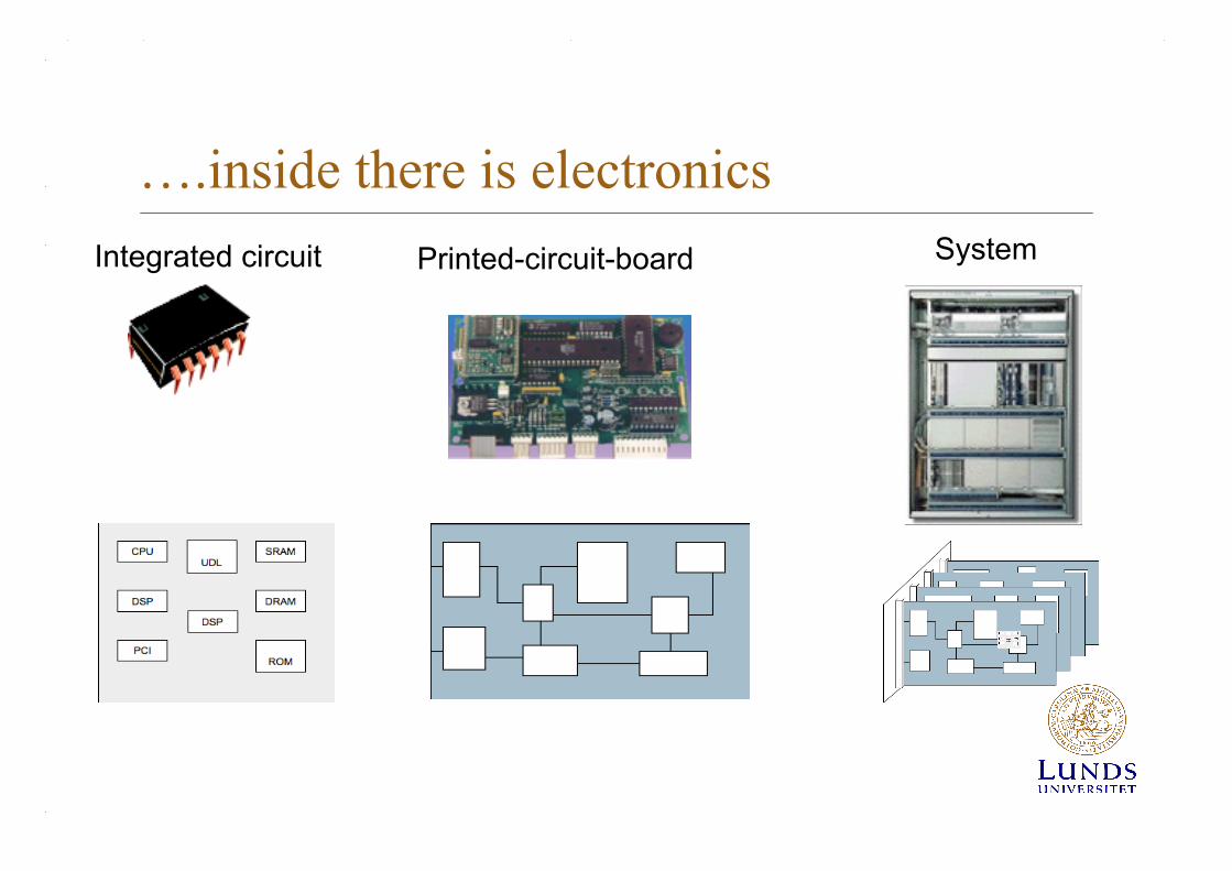
Building electronics
Array of Analog PSoC Blocks
SRAMMemory
I/O Ports
Global I/OProgrammable Interconnect
Array of Digital PSoC Blocks
Analog InputMuxing
DBA00
ACA00
DBA03
DBA02
DBA01
DCA04
DCA07
DCA06
DCA05
Analog OutputDrivers
P1
P0
ComparatorOutputs
Clocks toAnalog
P3
P2
P4
P5
ASA10
ASB20
ACA01
ASB11
ASA21
ACA02
ASA12
ASB22
ACA03
ASB13
ASA23
Internal System Bus
M8C CPUCore
Flash ProgramMemory
MACMultiply
Accumulate
Decimator Watchdog/Sleep Timer LVD/POR Interrupt
Controller
Oscillatorand PLL
Production Product
Array of Analog PSoC Blocks
SRAMMemory
I/O Ports
Global I/OProgrammable Interconnect
Array of Digital PSoC Blocks
Analog InputMuxing
DBA00
ACA00
DBA03
DBA02
DBA01
DCA04
DCA07
DCA06
DCA05
Analog OutputDrivers
P1
P0
ComparatorOutputs
Clocks toAnalog
P3
P2
P4
P5
ASA10
ASB20
ACA01
ASB11
ASA21
ACA02
ASA12
ASB22
ACA03
ASB13
ASA23
Internal System Bus
M8C CPUCore
Flash ProgramMemory
MACMultiply
Accumulate
Decimator Watchdog/Sleep Timer LVD/POR Interrupt
Controller
Oscillatorand PLL
Design specification
Design
Your new smartphone
• Let say your new smartphone does not work – Is there warranty, you get it repaired or replaced
• When the manufacturer received a customer return – Try to figure out what is wrong with the product
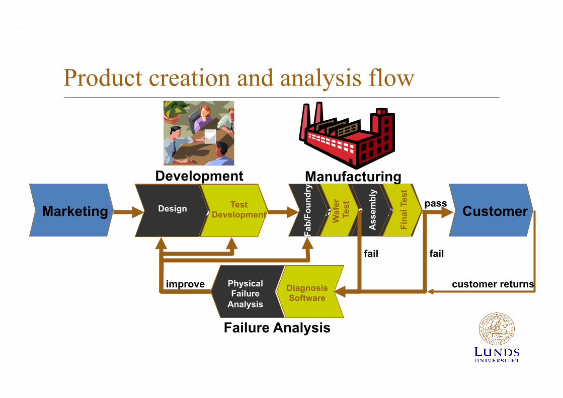
Product creation and analysis flow Failure Analysis Physical
Failure Analysis
Diagnosis Software
Failure Analysis
Development Manufacturing Marketing Customer Design Test Development W
afer
Te
st
Ass
embl
y
Fina
l Tes
t
Manufacturing
Fab/
Foun
dry
Development
customer returns
fail fail
pass
improve
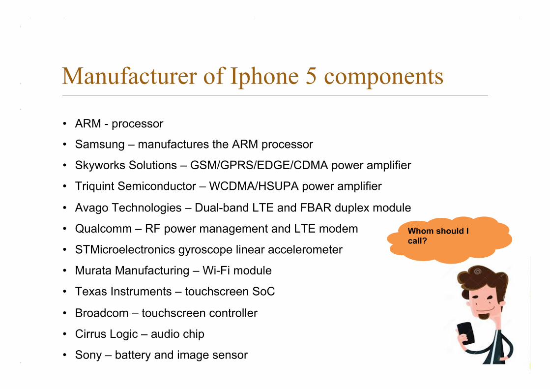
Manufacturer of Iphone 5 components
• ARM - processor
• Samsung – manufactures the ARM processor
• Skyworks Solutions – GSM/GPRS/EDGE/CDMA power amplifier
• Triquint Semiconductor – WCDMA/HSUPA power amplifier
• Avago Technologies – Dual-band LTE and FBAR duplex module
• Qualcomm – RF power management and LTE modem
• STMicroelectronics gyroscope linear accelerometer
• Murata Manufacturing – Wi-Fi module
• Texas Instruments – touchscreen SoC
• Broadcom – touchscreen controller
• Cirrus Logic – audio chip
• Sony – battery and image sensor
Whom should I call?
One component (IC) SUN SPARC M7 10 000 000 000
transistors
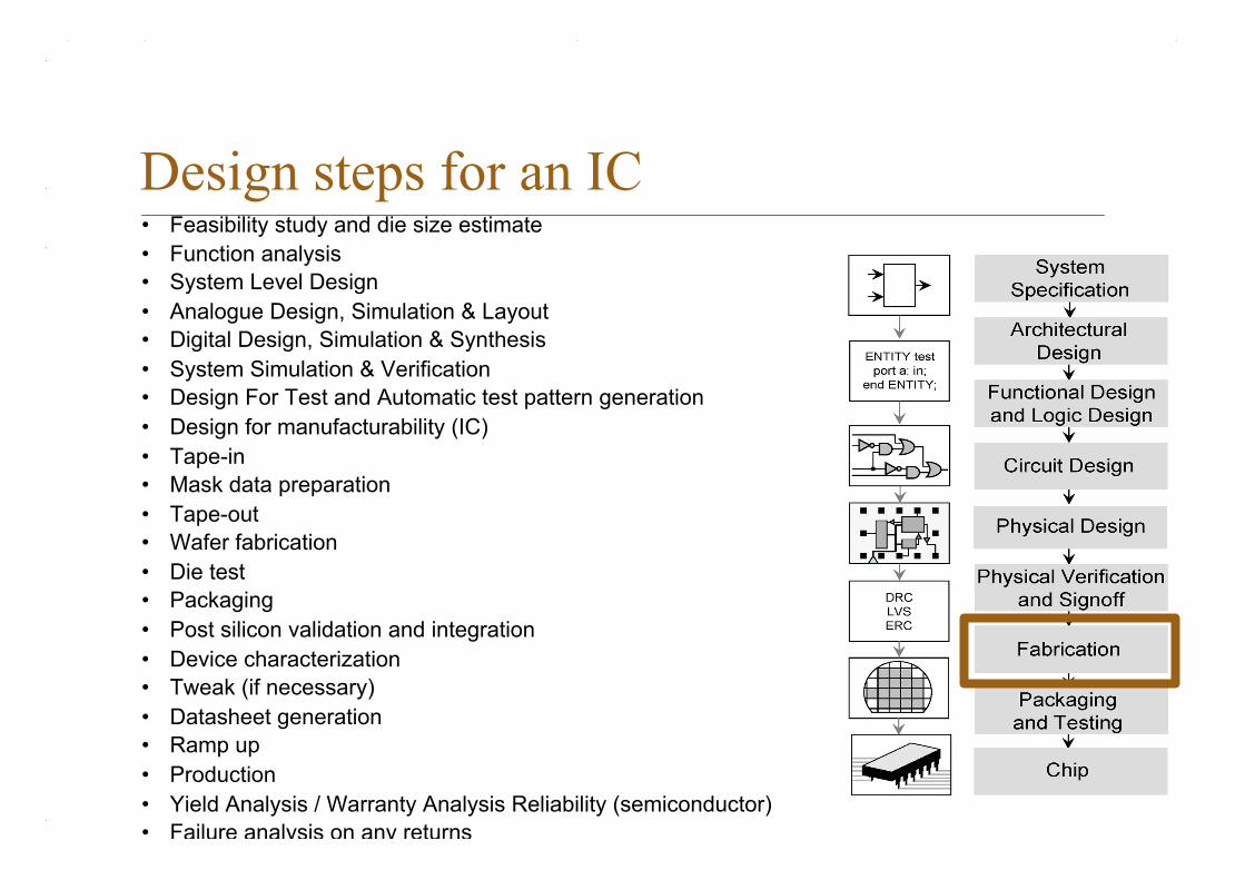
Design steps for an IC • Feasibility study and die size estimate • Function analysis • System Level Design • Analogue Design, Simulation & Layout • Digital Design, Simulation & Synthesis • System Simulation & Verification • Design For Test and Automatic test pattern generation • Design for manufacturability (IC) • Tape-in • Mask data preparation • Tape-out • Wafer fabrication • Die test • Packaging • Post silicon validation and integration • Device characterization • Tweak (if necessary) • Datasheet generation • Ramp up • Production • Yield Analysis / Warranty Analysis Reliability (semiconductor) • Failure analysis on any returns • Plan for next generation chip using production information if possible
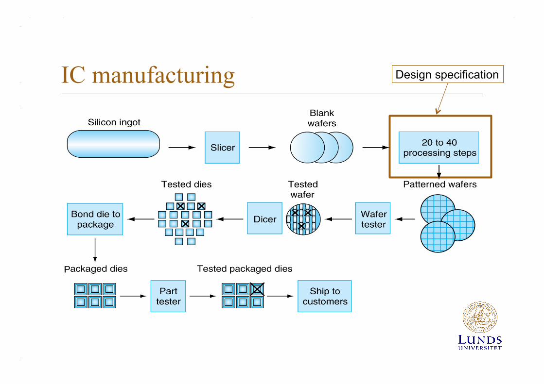
IC manufacturing Design specification
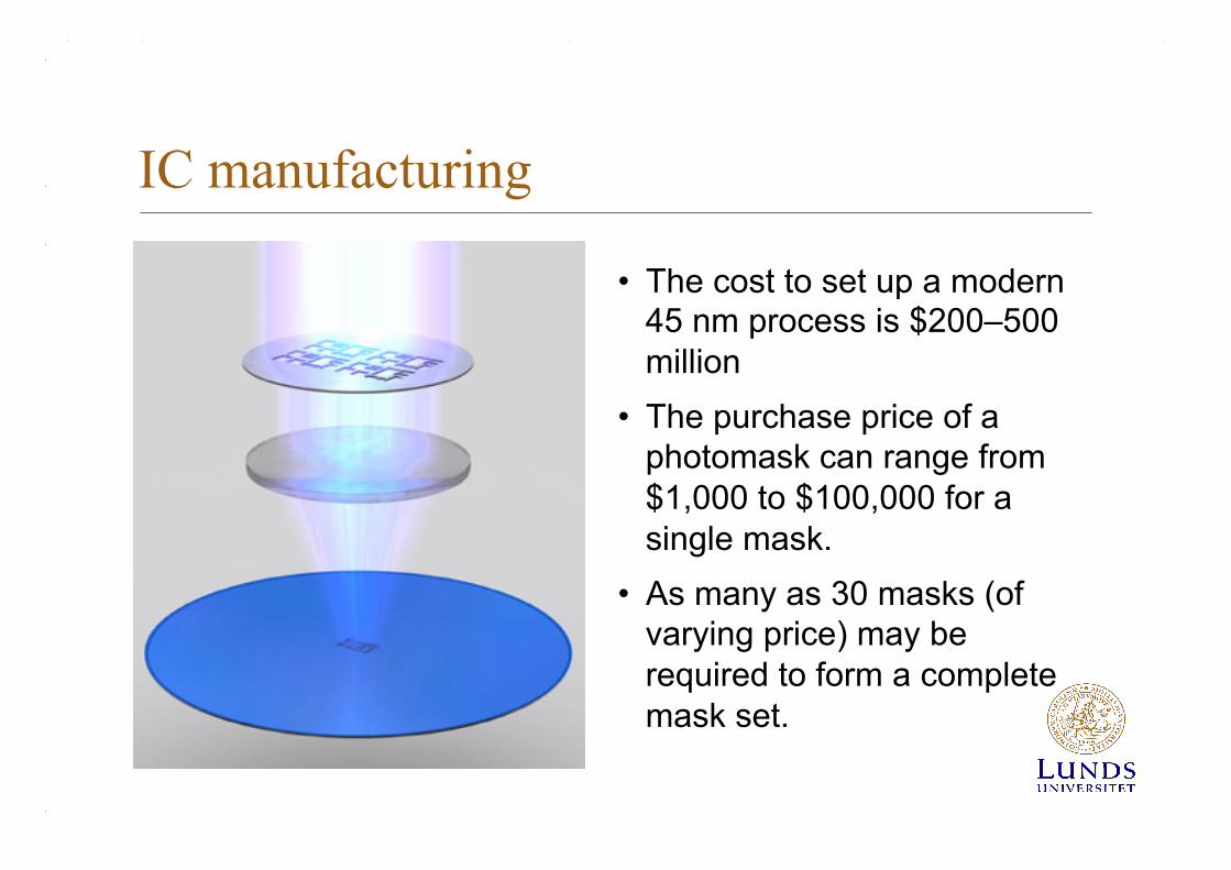
IC manufacturing
• The cost to set up a modern 45 nm process is $200–500 million
• The purchase price of a photomask can range from $1,000 to $100,000 for a single mask.
• As many as 30 masks (of varying price) may be required to form a complete mask set.
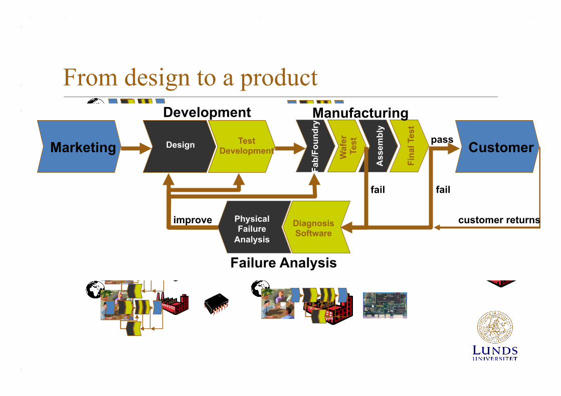
From design to a product
Failure Analysis
Development Manufacturing
Failure Analysis
Development Manufacturing
Failure Analysis
Development Manufacturing
Failure Analysis
Development Manufacturing
Failure Analysis
Development Manufacturing
Failure Analysis
Development Manufacturing
Failure Analysis
Development Manufacturing
Failure Analysis
Development Manufacturing
Failure Analysis
Development Manufacturing
Failure Analysis
Development Manufacturing
Physical Failure
Analysis
Diagnosis Software
Failure Analysis
Marketing Customer Design Test Development W
afer
Te
st
Ass
embl
y
Fina
l Tes
t
Manufacturing
Fab/
Foun
dry
Development
customer returns
fail fail
pass
improve
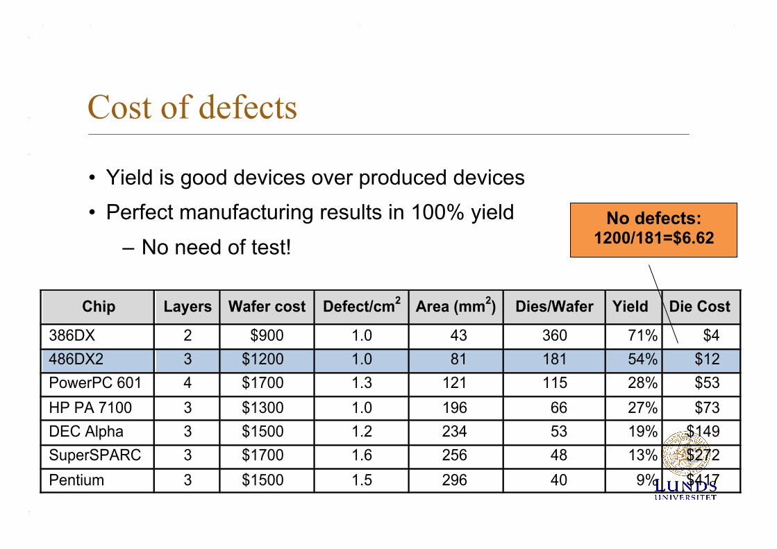
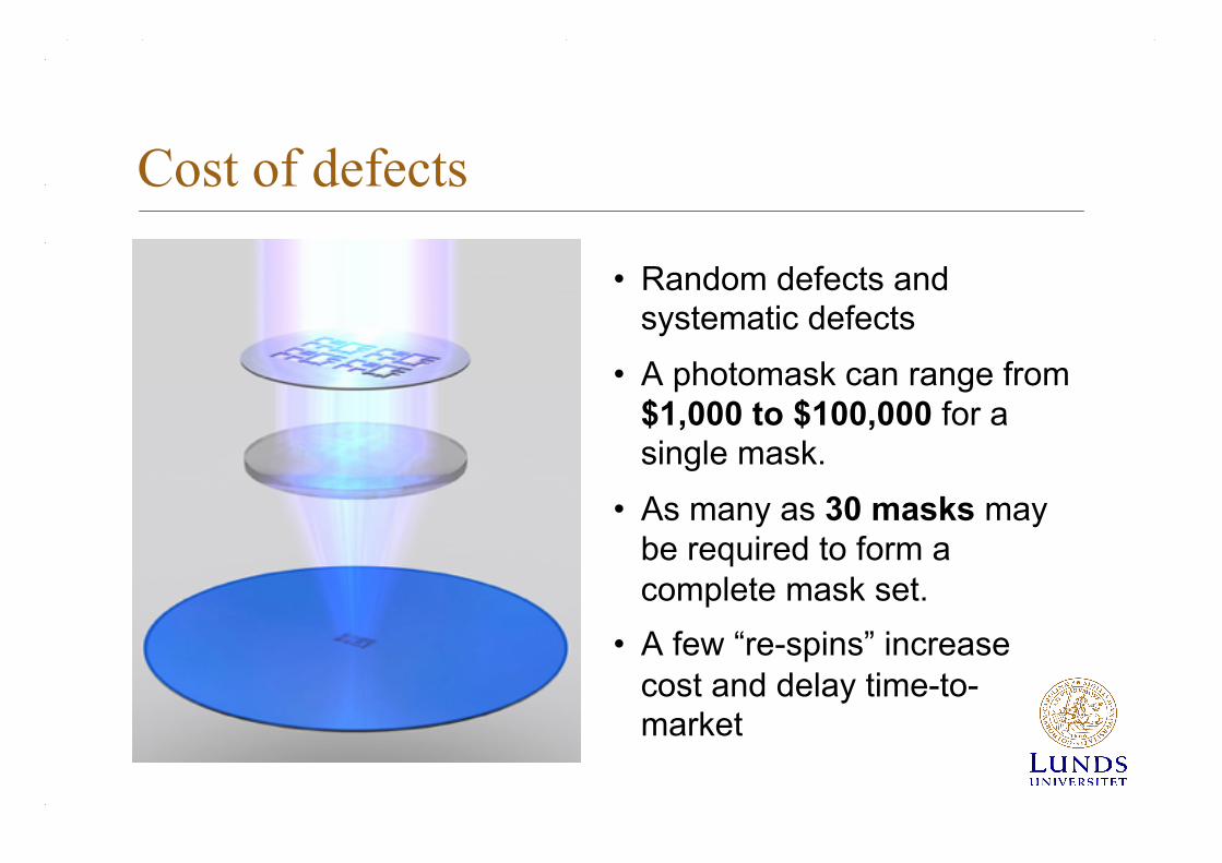
Cost of defects
• Yield is good devices over produced devices • Perfect manufacturing results in 100% yield
– No need of test!
Chip Layers Wafer cost Defect/cm2 Area (mm2) Dies/Wafer Yield Die Cost
386DX 2 $900 1.0 43 360 71% $4 486DX2 3 $1200 1.0 81 181 54% $12 PowerPC 601 4 $1700 1.3 121 115 28% $53 HP PA 7100 3 $1300 1.0 196 66 27% $73 DEC Alpha 3 $1500 1.2 234 53 19% $149 SuperSPARC 3 $1700 1.6 256 48 13% $272 Pentium 3 $1500 1.5 296 40 9% $417
No defects: 1200/181=$6.62
Cost of defects
• Random defects and systematic defects
• A photomask can range from $1,000 to $100,000 for a single mask.
• As many as 30 masks may be required to form a complete mask set.
• A few “re-spins” increase cost and delay time-to-market
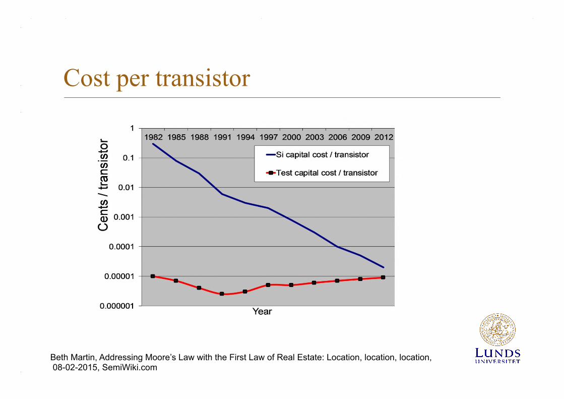
Cost per transistor
Beth Martin, Addressing Moore’s Law with the First Law of Real Estate: Location, location, location, 08-02-2015, SemiWiki.com
Cost for returns and repair
• The total cost of consumer electronics returns and repairs attributed to U.S. consumers was estimated at $13.8 billion (2007).
– That is about 500 SEK per person/year • No Trouble Found (NTF) is referring to a system or
component that has been returned to the manufacturer or distributor for warranty replacement or service repair, but operates properly when tested. This situation is also referred to as No Defect Found (NDF) and No Fault Found (NFF).
– Total cost of return and repair: $13.8 billion (2007) of which 20% is NTF (100 SEK per person/year)
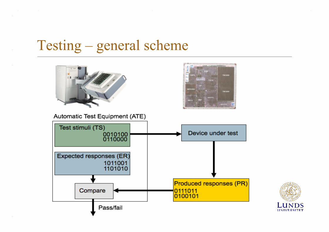
Testing – general scheme
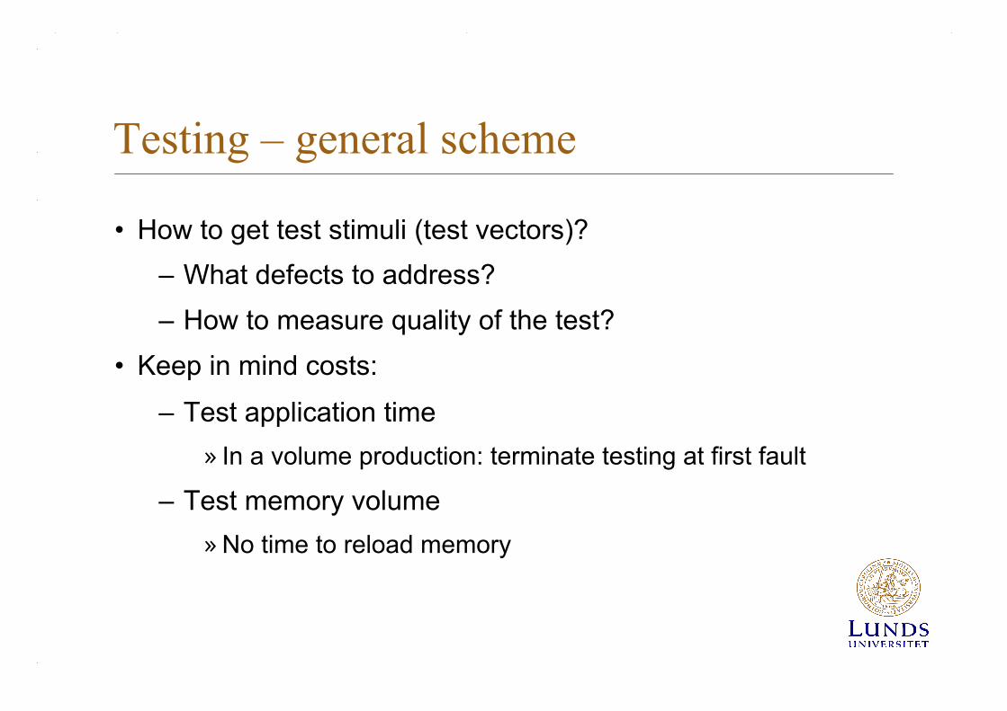
Testing – general scheme
• How to get test stimuli (test vectors)? – What defects to address? – How to measure quality of the test?
• Keep in mind costs:
– Test application time » In a volume production: terminate testing at first fault
– Test memory volume » No time to reload memory
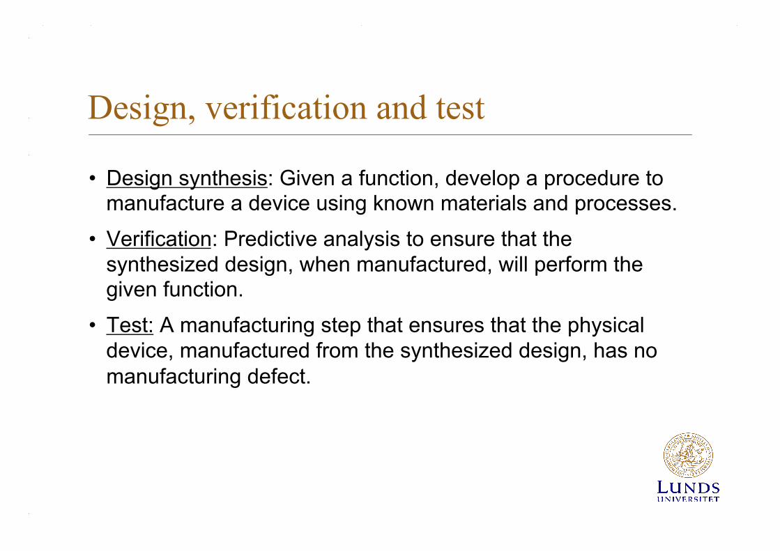
Design, verification and test
• Design synthesis: Given a function, develop a procedure to manufacture a device using known materials and processes.
• Verification: Predictive analysis to ensure that the synthesized design, when manufactured, will perform the given function.
• Test: A manufacturing step that ensures that the physical device, manufactured from the synthesized design, has no manufacturing defect.
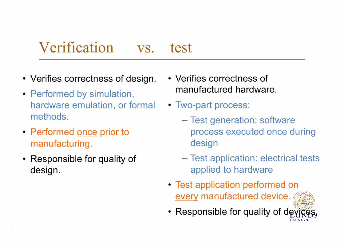
Verification vs. test
• Verifies correctness of design. • Performed by simulation,
hardware emulation, or formal methods.
• Performed once prior to manufacturing.
• Responsible for quality of design.
• Verifies correctness of manufactured hardware.
• Two-part process: – Test generation: software
process executed once during design
– Test application: electrical tests applied to hardware
• Test application performed on every manufactured device.
• Responsible for quality of devices.
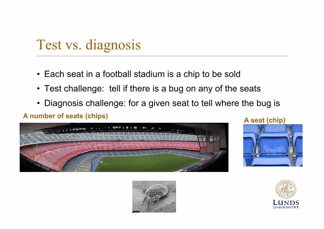
Test vs. diagnosis
• Each seat in a football stadium is a chip to be sold • Test challenge: tell if there is a bug on any of the seats • Diagnosis challenge: for a given seat to tell where the bug is
A seat (chip) A number of seats (chips)
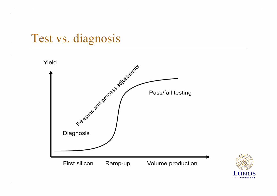
Test vs. diagnosis
Yield
First silicon Ramp-up Volume production
Diagnosis
Pass/fail testing
Defects

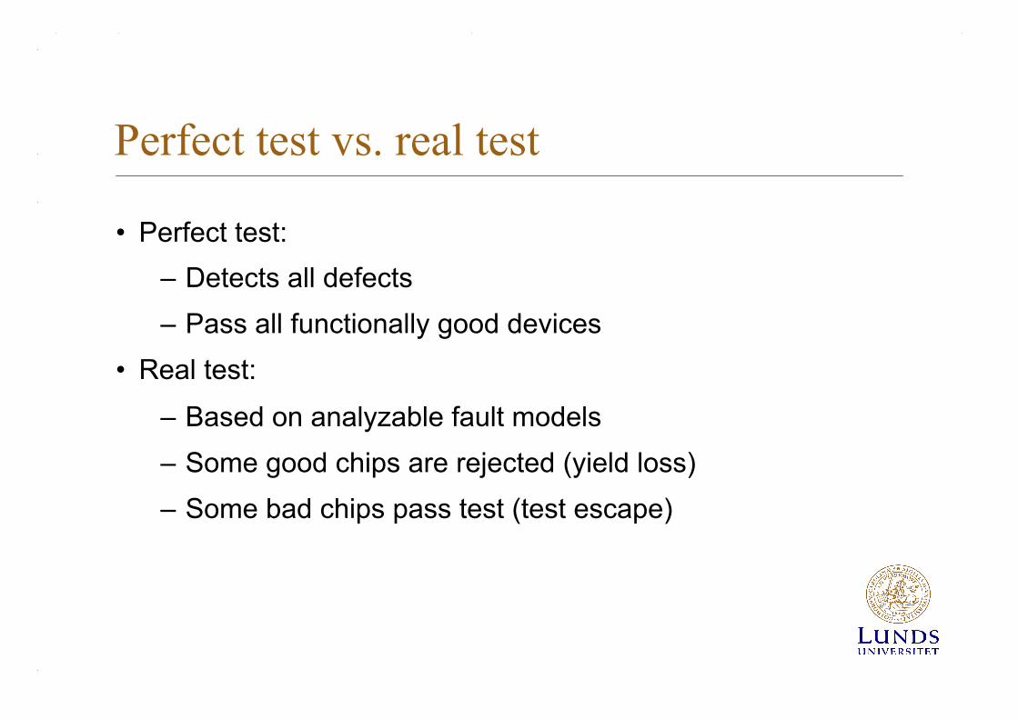
Perfect test vs. real test
• Perfect test: – Detects all defects – Pass all functionally good devices
• Real test:
– Based on analyzable fault models – Some good chips are rejected (yield loss) – Some bad chips pass test (test escape)
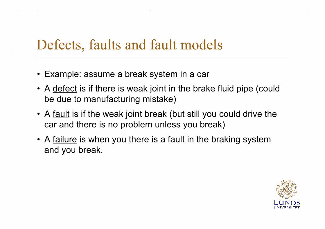
Defects, faults and fault models
• Example: assume a break system in a car • A defect is if there is weak joint in the brake fluid pipe (could
be due to manufacturing mistake)
• A fault is if the weak joint break (but still you could drive the car and there is no problem unless you break)
• A failure is when you there is a fault in the braking system and you break.
Defects, faults and fault models
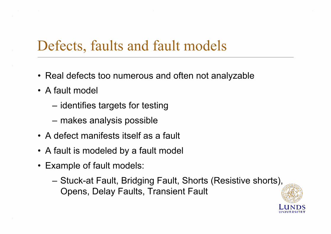
• Real defects too numerous and often not analyzable • A fault model
– identifies targets for testing – makes analysis possible
• A defect manifests itself as a fault • A fault is modeled by a fault model • Example of fault models:
– Stuck-at Fault, Bridging Fault, Shorts (Resistive shorts), Opens, Delay Faults, Transient Fault
Defects, faults and fault models
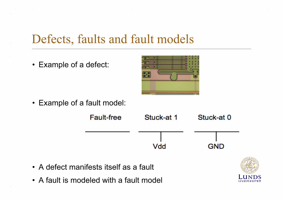
• Example of a defect:
• Example of a fault model:
• A defect manifests itself as a fault
• A fault is modeled with a fault model
Defects, faults, fault models
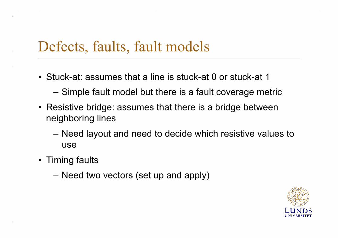
• Stuck-at: assumes that a line is stuck-at 0 or stuck-at 1 – Simple fault model but there is a fault coverage metric
• Resistive bridge: assumes that there is a bridge between neighboring lines
– Need layout and need to decide which resistive values to use
• Timing faults – Need two vectors (set up and apply)
Fault classes
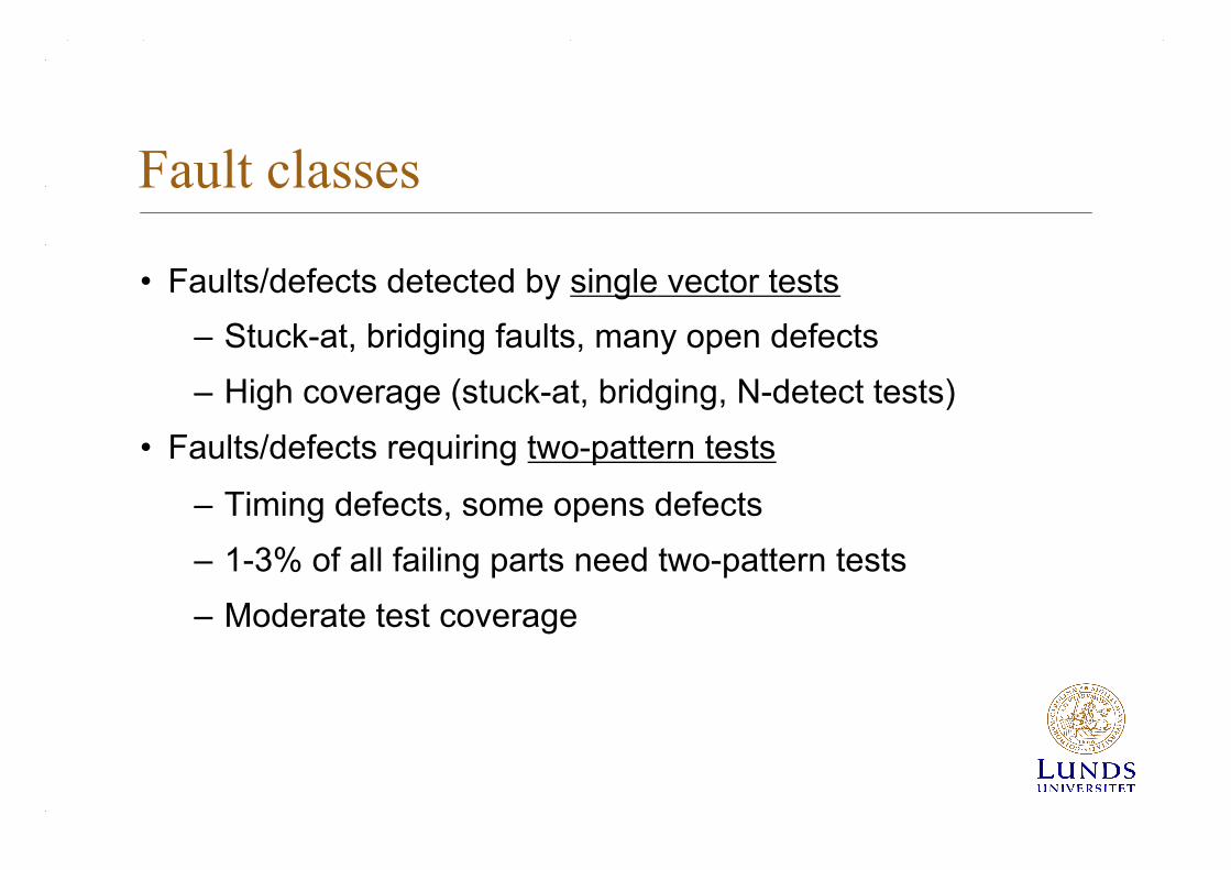
• Faults/defects detected by single vector tests – Stuck-at, bridging faults, many open defects – High coverage (stuck-at, bridging, N-detect tests)
• Faults/defects requiring two-pattern tests
– Timing defects, some opens defects – 1-3% of all failing parts need two-pattern tests – Moderate test coverage
Testing basics
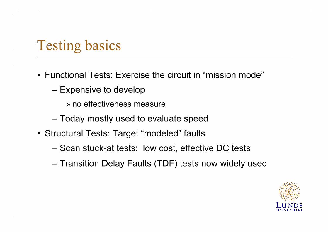
• Functional Tests: Exercise the circuit in “mission mode” – Expensive to develop
» no effectiveness measure
– Today mostly used to evaluate speed • Structural Tests: Target “modeled” faults
– Scan stuck-at tests: low cost, effective DC tests
– Transition Delay Faults (TDF) tests now widely used
Perfect test vs. real test
• Perfect test: – Detects all defects – Pass all functionally good devices
• Real test:
– Based on analyzable fault models – Some good chips are rejected (yield loss) – Some bad chips pass test (test escape)
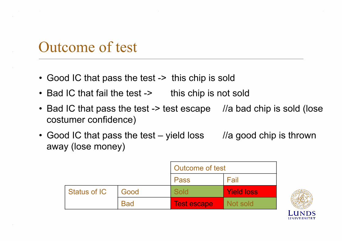
Outcome of test
• Good IC that pass the test -> this chip is sold • Bad IC that fail the test -> this chip is not sold • Bad IC that pass the test -> test escape //a bad chip is sold (lose
costumer confidence)
• Good IC that pass the test – yield loss //a good chip is thrown away (lose money)
Outcome of test Pass Fail
Status of IC Good Sold Yield loss Bad Test escape Not sold
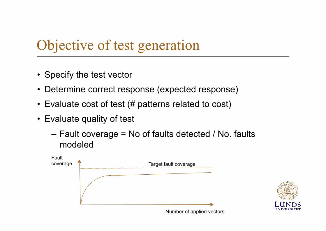
Objective of test generation
• Specify the test vector • Determine correct response (expected response) • Evaluate cost of test (# patterns related to cost) • Evaluate quality of test
– Fault coverage = No of faults detected / No. faults modeled
Number of applied vectors
Fault coverage Target fault coverage
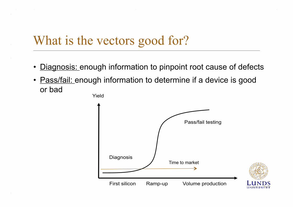
What is the vectors good for?
• Diagnosis: enough information to pinpoint root cause of defects • Pass/fail: enough information to determine if a device is good
or bad
Yield
First silicon Ramp-up Volume production
Diagnosis
Pass/fail testing
Time to market
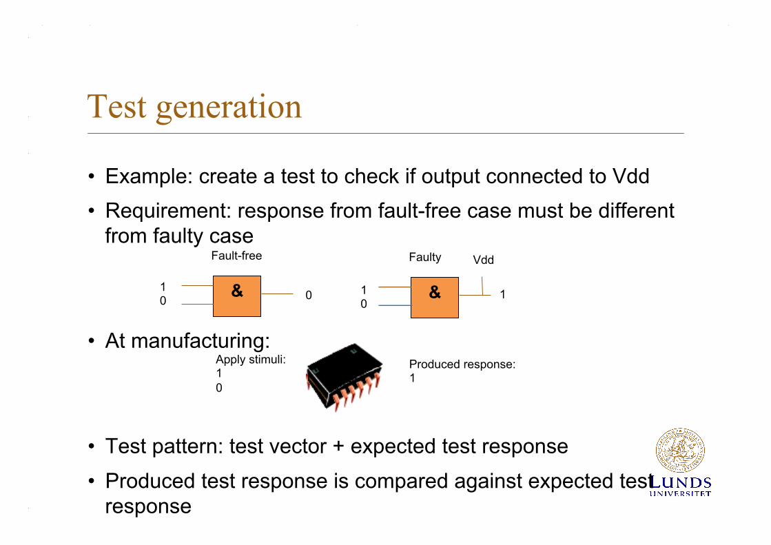
Test generation
• Example: create a test to check if output connected to Vdd • Requirement: response from fault-free case must be different
from faulty case
• At manufacturing:
• Test pattern: test vector + expected test response • Produced test response is compared against expected test
response
&
Fault-free
&
Faulty Vdd
1 0
1 0
0 1
Apply stimuli: 1 0
Produced response: 1
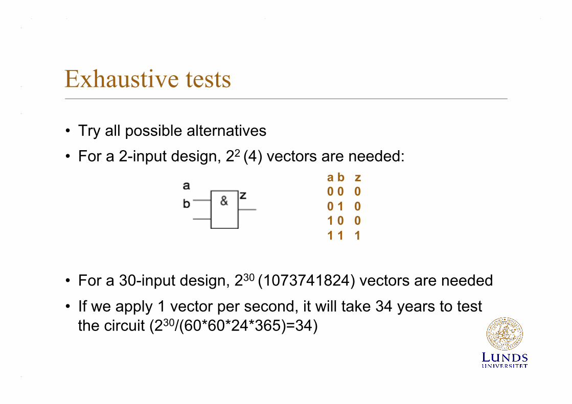
Exhaustive tests
• Try all possible alternatives • For a 2-input design, 22 (4) vectors are needed:
• For a 30-input design, 230 (1073741824) vectors are needed • If we apply 1 vector per second, it will take 34 years to test
the circuit (230/(60*60*24*365)=34)
a b z 0 0 0 0 1 0 1 0 0 1 1 1
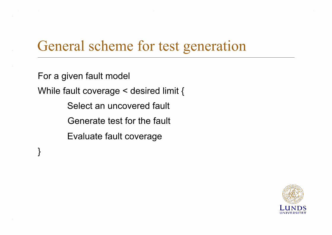
General scheme for test generation
For a given fault model While fault coverage < desired limit {
Select an uncovered fault Generate test for the fault
Evaluate fault coverage }
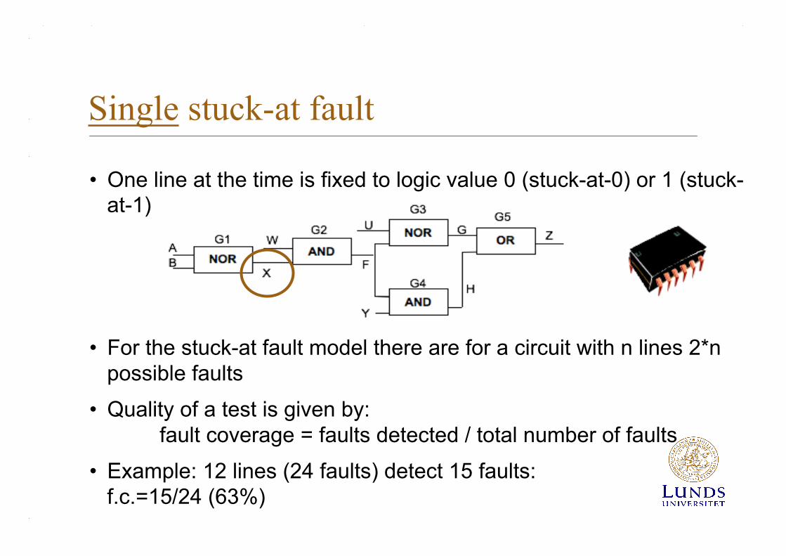
Single stuck-at fault
• One line at the time is fixed to logic value 0 (stuck-at-0) or 1 (stuck-at-1)
• For the stuck-at fault model there are for a circuit with n lines 2*n possible faults
• Quality of a test is given by: fault coverage = faults detected / total number of faults
• Example: 12 lines (24 faults) detect 15 faults: f.c.=15/24 (63%)
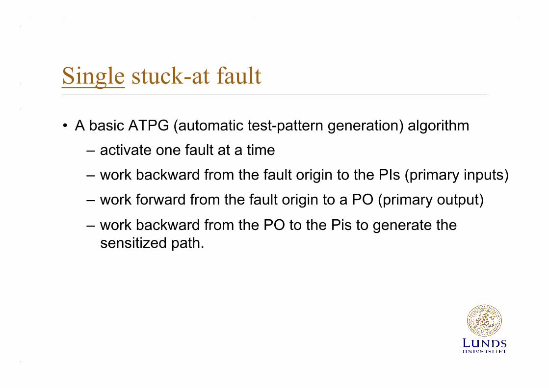
Single stuck-at fault
• A basic ATPG (automatic test-pattern generation) algorithm – activate one fault at a time – work backward from the fault origin to the PIs (primary inputs) – work forward from the fault origin to a PO (primary output)
– work backward from the PO to the Pis to generate the sensitized path.
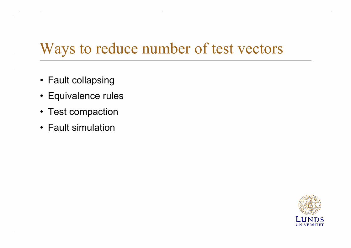
Ways to reduce number of test vectors
• Fault collapsing • Equivalence rules • Test compaction • Fault simulation
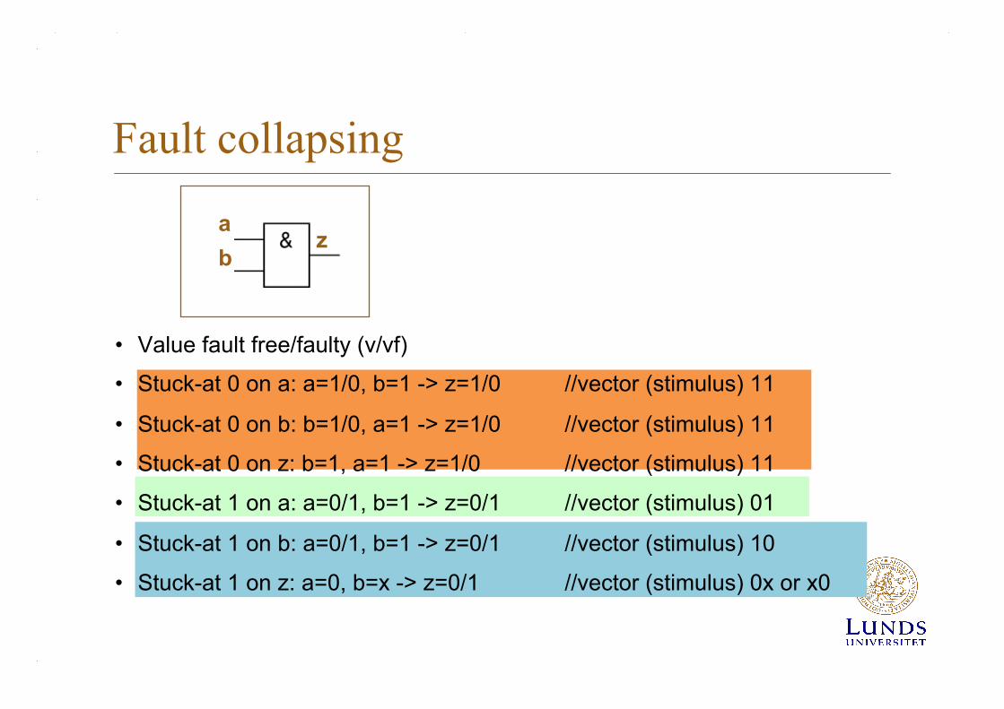
Fault collapsing
• Value fault free/faulty (v/vf)
• Stuck-at 0 on a: a=1/0, b=1 -> z=1/0 //vector (stimulus) 11
• Stuck-at 0 on b: b=1/0, a=1 -> z=1/0 //vector (stimulus) 11
• Stuck-at 0 on z: b=1, a=1 -> z=1/0 //vector (stimulus) 11
• Stuck-at 1 on a: a=0/1, b=1 -> z=0/1 //vector (stimulus) 01
• Stuck-at 1 on b: a=0/1, b=1 -> z=0/1 //vector (stimulus) 10
• Stuck-at 1 on z: a=0, b=x -> z=0/1 //vector (stimulus) 0x or x0
a b
z
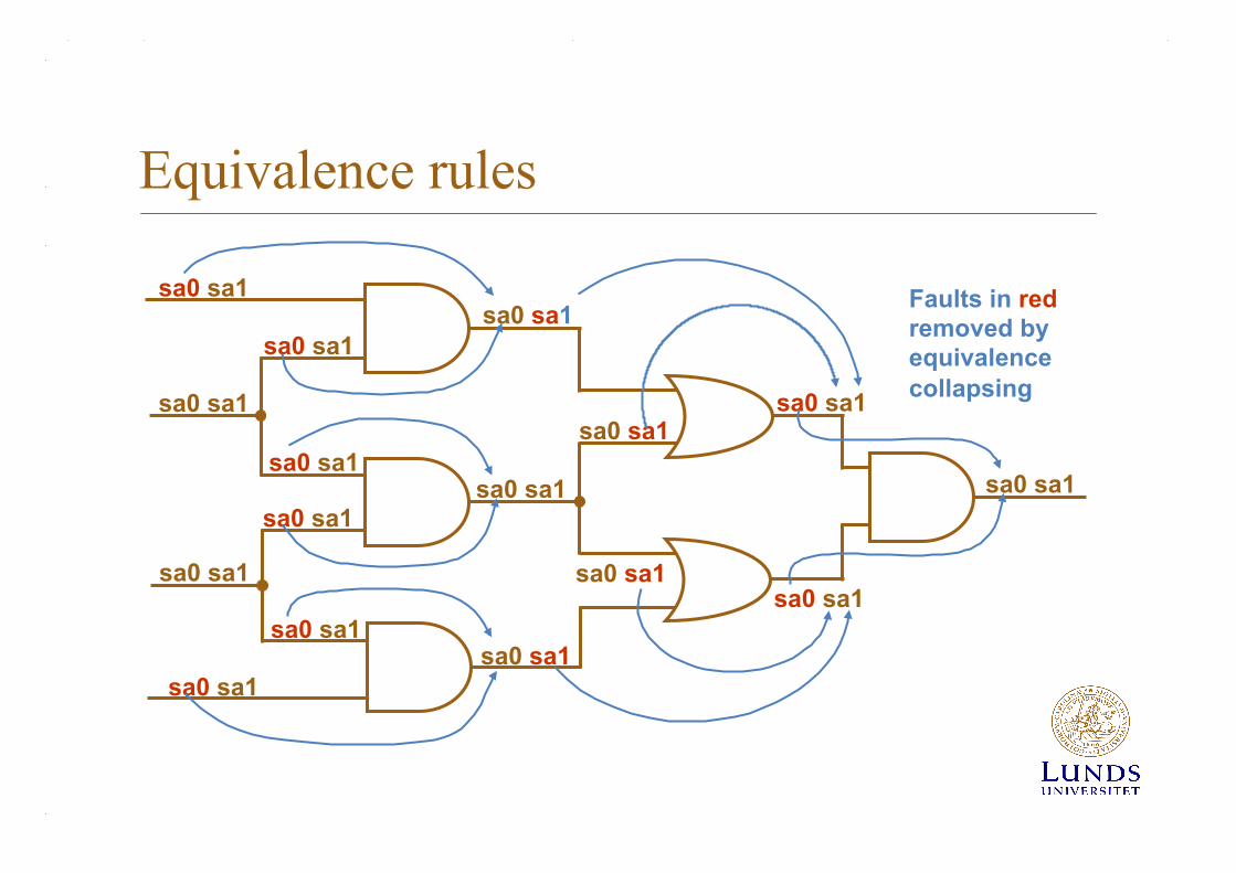
Equivalence rules
sa0 sa1 sa0 sa1
sa0 sa1
sa0 sa1
sa0 sa1
sa0 sa1
sa0 sa1
sa0 sa1
sa0 sa1
sa0 sa1
sa0 sa1
sa0 sa1
sa0 sa1
sa0 sa1
sa0 sa1
sa0 sa1
Faults in red removed by equivalence collapsing
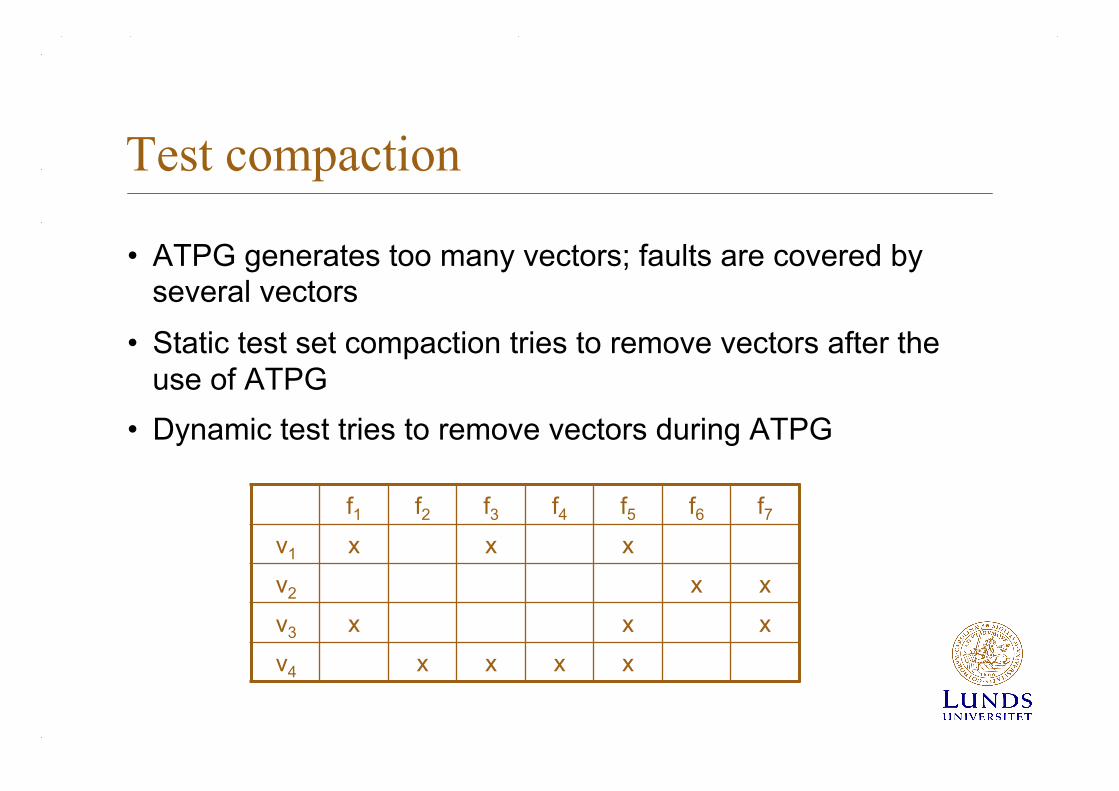
Test compaction
• ATPG generates too many vectors; faults are covered by several vectors
• Static test set compaction tries to remove vectors after the use of ATPG
• Dynamic test tries to remove vectors during ATPG
f1 f2 f3 f4 f5 f6 f7
v1 x x x v2 x x v3 x x x v4 x x x x
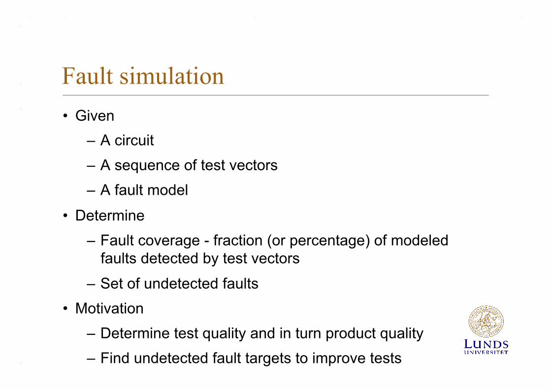
Fault simulation • Given
– A circuit – A sequence of test vectors – A fault model
• Determine – Fault coverage - fraction (or percentage) of modeled
faults detected by test vectors
– Set of undetected faults • Motivation
– Determine test quality and in turn product quality – Find undetected fault targets to improve tests
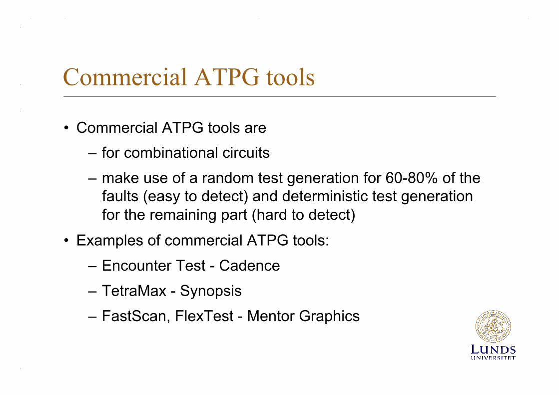
Commercial ATPG tools
• Commercial ATPG tools are – for combinational circuits – make use of a random test generation for 60-80% of the
faults (easy to detect) and deterministic test generation for the remaining part (hard to detect)
• Examples of commercial ATPG tools: – Encounter Test - Cadence – TetraMax - Synopsis – FastScan, FlexTest - Mentor Graphics
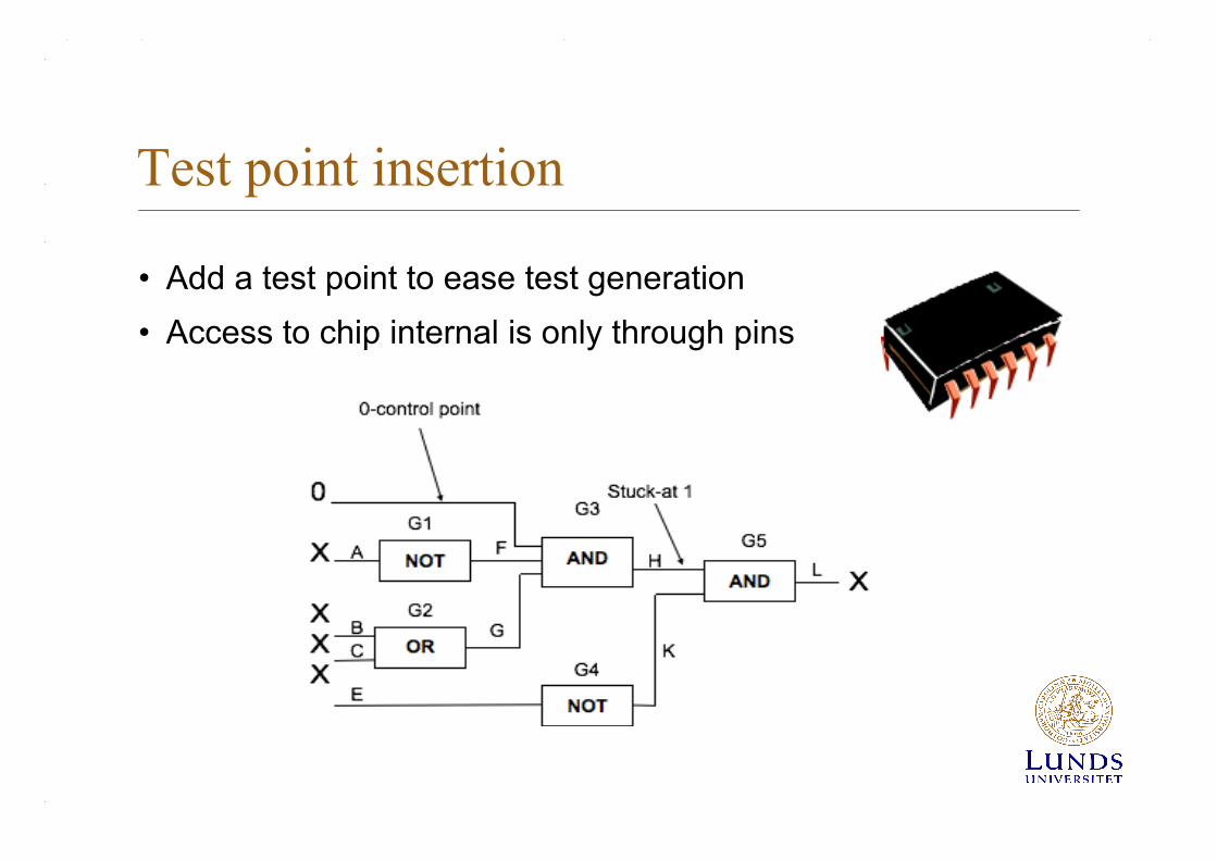
Test point insertion
• Add a test point to ease test generation • Access to chip internal is only through pins
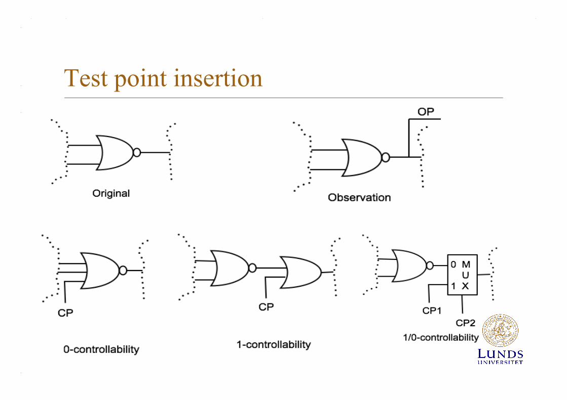
Test point insertion
Scan
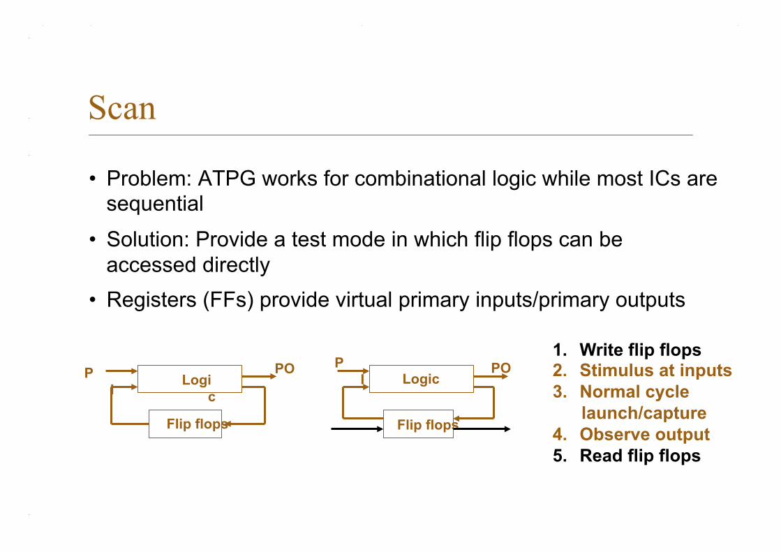
• Problem: ATPG works for combinational logic while most ICs are sequential
• Solution: Provide a test mode in which flip flops can be accessed directly
• Registers (FFs) provide virtual primary inputs/primary outputs
Logic
PI
PO
Flip flops
Logic P
IPO
Flip flops
1. Write flip flops 2. Stimulus at inputs 3. Normal cycle
launch/capture 4. Observe output 5. Read flip flops
Scan
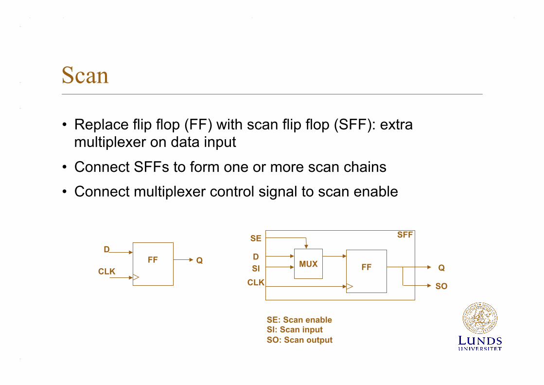
• Replace flip flop (FF) with scan flip flop (SFF): extra multiplexer on data input
• Connect SFFs to form one or more scan chains • Connect multiplexer control signal to scan enable
FF MUX
CLK
SE
Q
SO
D SI
FF CLK
Q D
SFF
SE: Scan enable SI: Scan input SO: Scan output
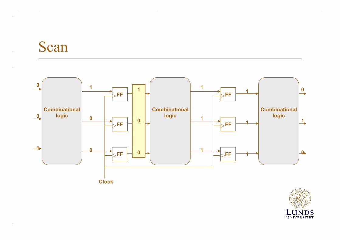
Scan
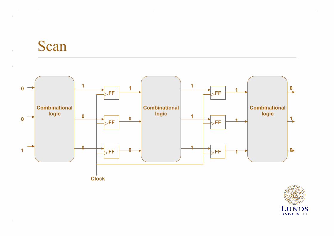
FF
Combinational logic
FF
Combinational logic
Combinational logic
FF
FF
Clock
FF
FF
1 0 0
1 0 0
1 1 1
1 1 1
0 1 0
0 0 1
Scan
FF
Combinational logic
FF
Combinational logic
Combinational logic
FF
FF
Clock
FF
FF
0 0 1
1 0 0
1 0 0
1 1 1
1 1 1
0 1 0
Scan
FF
Combinational logic
MUX FF MUX
Combinational logic
Combinational logic
FF MUX
FF MUX
Scan enable
Clock Scan Input Scan Output
FF MUX
FF MUX
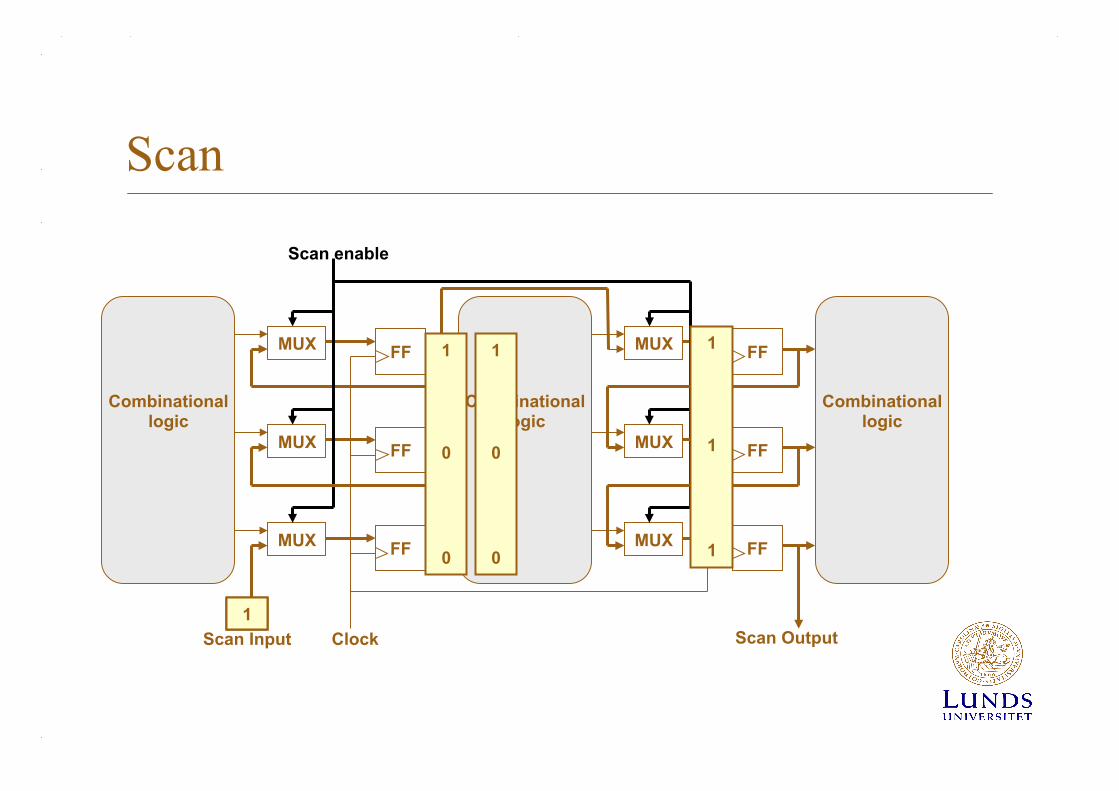
Scan
Combinational logic
FF MUX
FF MUX
FF MUX
Scan enable
FF MUX
Combinational logic
Combinational logic
Clock Scan Input Scan Output
FF MUX
FF MUX
0 0 1
1 0 0
1 1 1
1 0 0
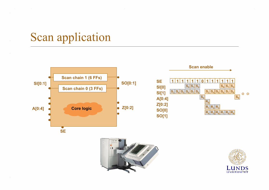
Scan application
Scan chain 1 (6 FFs)
Scan chain 0 (3 FFs)
SE
SI[0:1] SO[0:1]
A[0:4] Z[0:2] Core logic
SE SI[0] SI[1] A[0:4] Z[0:2] SO[0] SO[1]
1 1 1 1 1 1 0 1 1 1 1 1 1 S0 S1 S2
S3 S4 S5 S6 S7 S8
S9
R0
R1 R2 R3
R4 R5 R6 R7 R8 R9
S0 S1 S2
S3 S4 S5 S6 S7 S8
S9
Scan enable
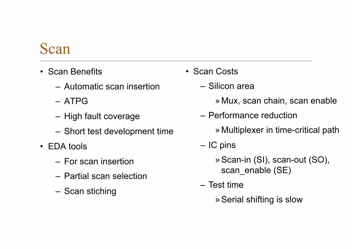
• Scan Costs
– Silicon area
» Mux, scan chain, scan enable
– Performance reduction
» Multiplexer in time-critical path
– IC pins
» Scan-in (SI), scan-out (SO), scan_enable (SE)
– Test time
» Serial shifting is slow
Scan • Scan Benefits
– Automatic scan insertion
– ATPG
– High fault coverage
– Short test development time
• EDA tools
– For scan insertion
– Partial scan selection
– Scan stiching
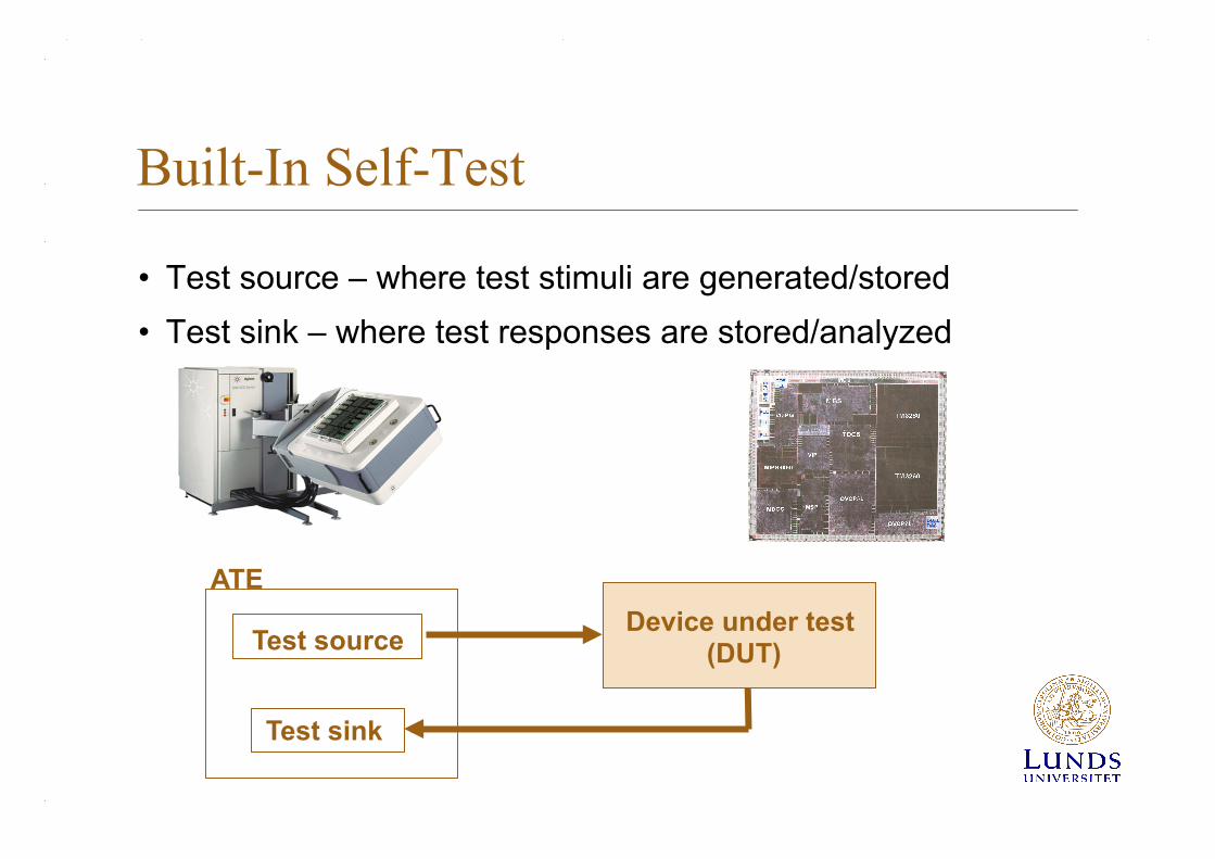
Built-In Self-Test
• Test source – where test stimuli are generated/stored • Test sink – where test responses are stored/analyzed
Device under test (DUT)
Test source
Test sink
ATE
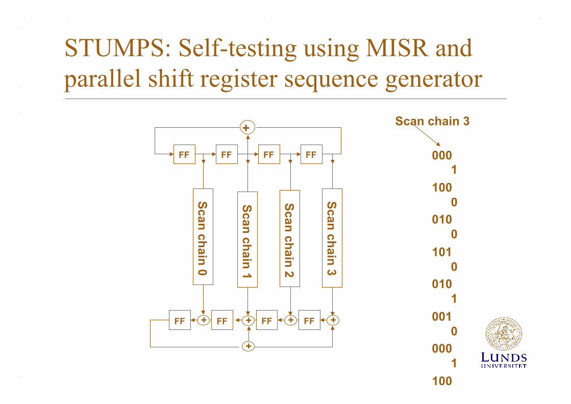
STUMPS: Self-testing using MISR and parallel shift register sequence generator
Scan chain 1
Scan chain 0
Scan chain 2
Scan chain 3
+
FF FF FF FF
FF FF FF FF
+
+
+ + +
0001
1000
0100
1010
0101
0010
0001
1000
0100
1010
0101
0010
0001
Scan chain 3
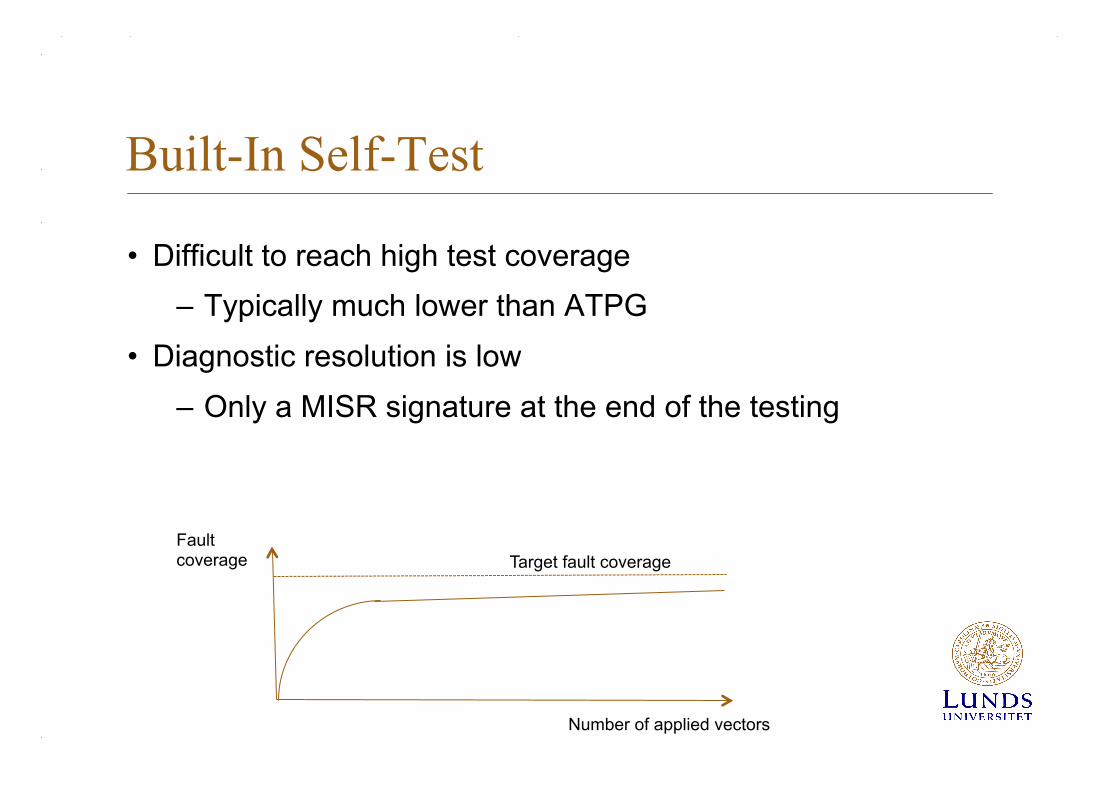
Built-In Self-Test
• Difficult to reach high test coverage – Typically much lower than ATPG
• Diagnostic resolution is low – Only a MISR signature at the end of the testing
Number of applied vectors
Fault coverage Target fault coverage
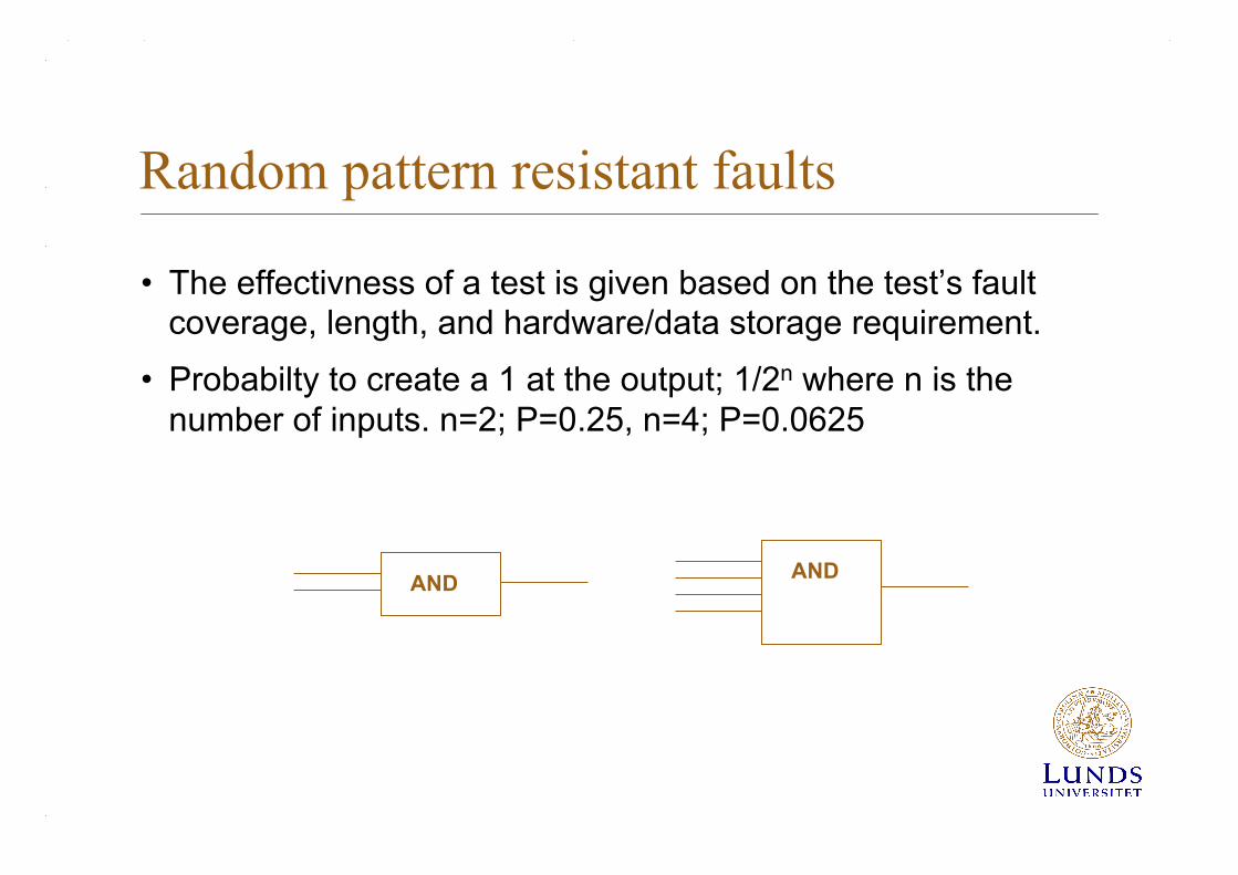
Random pattern resistant faults
• The effectivness of a test is given based on the test’s fault coverage, length, and hardware/data storage requirement.
• Probabilty to create a 1 at the output; 1/2n where n is the number of inputs. n=2; P=0.25, n=4; P=0.0625
AND AND
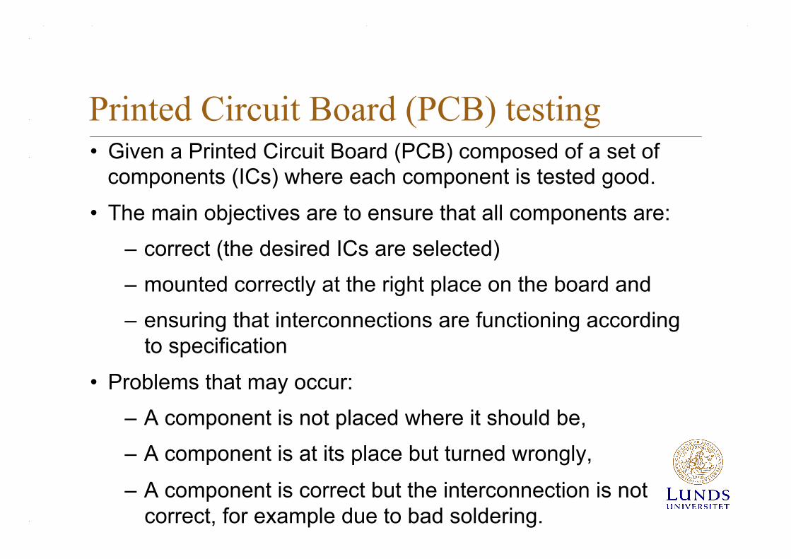
Printed Circuit Board (PCB) testing • Given a Printed Circuit Board (PCB) composed of a set of
components (ICs) where each component is tested good.
• The main objectives are to ensure that all components are: – correct (the desired ICs are selected) – mounted correctly at the right place on the board and – ensuring that interconnections are functioning according
to specification
• Problems that may occur: – A component is not placed where it should be, – A component is at its place but turned wrongly,
– A component is correct but the interconnection is not correct, for example due to bad soldering.
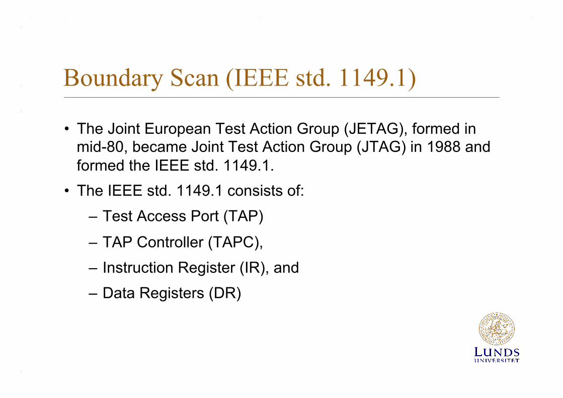
Boundary Scan (IEEE std. 1149.1)
• The Joint European Test Action Group (JETAG), formed in mid-80, became Joint Test Action Group (JTAG) in 1988 and formed the IEEE std. 1149.1.
• The IEEE std. 1149.1 consists of: – Test Access Port (TAP)
– TAP Controller (TAPC), – Instruction Register (IR), and – Data Registers (DR)
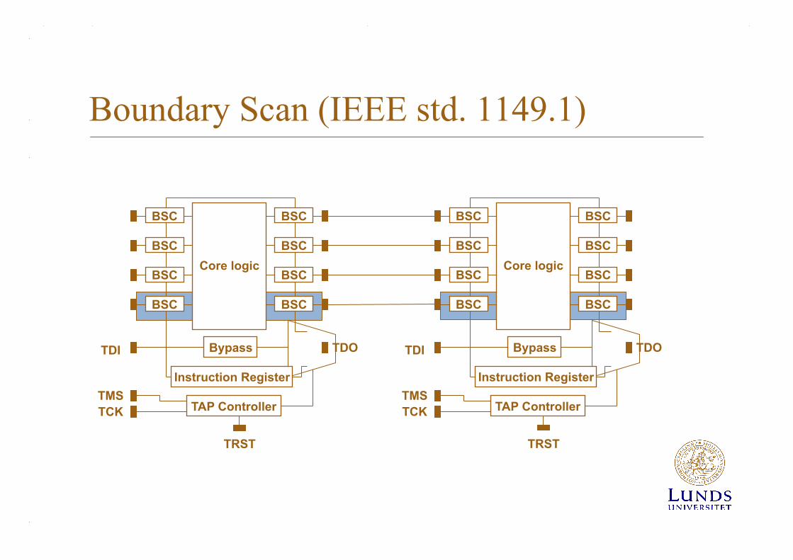
Boundary Scan (IEEE std. 1149.1)
Core logic BSC
TRST
TAP Controller
TDI
TMS TCK
BSC
TDO
BSC
BSC
BSC
BSC
BSC
BSC
Instruction Register
Bypass
Core logic BSC
TRST
TAP Controller
TDI
TMS TCK
BSC
TDO
BSC
BSC
BSC
BSC
BSC
BSC
Instruction Register
Bypass
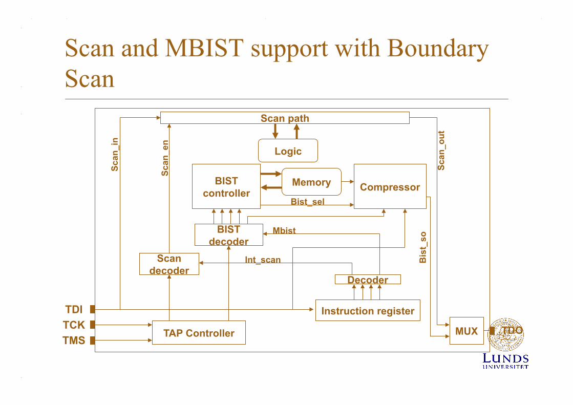
Scan and MBIST support with Boundary Scan
TDI
TMS TCK TDO
TAP Controller
Scan path
Logic
BIST decoder
Scan decoder
Instruction register
Decoder
MUX
Compressor Memory
Scan
_en
Scan
_in
Scan
_out
Int_scan
Mbist
Bis
t_so
BIST controller
Bist_sel
Conclusions
• Producing products with high quality, start work during design time
• After manufacturing: – every unit is tested to check for eventual defects – defective units are diagnosed to pin-point root cause
• To measure quality, there is a need of a metric that tells the quality of a test
• Important to keep cost at a minimum: – Test generation is done once but can take months – Test application takes seconds/minutes, but is applied to
every manufactured device
Future perspective
• Transistor count increase – More complexity – more transistors to check
• Access points (pins) do not increase with transistor count – Bandwidth problem (competition for pins)
• Smaller transistors (new defect types, process variations) – Not sufficient with manufacturing test and configuration
alone » Need to monitor/test/reconfigure/tune the system during
operation