Embed Size (px)
Citation preview
21-22 july 2005 C. de La Taille Electronics CERN Summer School 2005 1
Introduction to Electronics for High Energy Physics
C. de LA TAILLELAL Orsay
CERN Summer school 2005
21-22 july 2005 C. de La Taille Electronics CERN Summer School 2005 2
Outline
Course 1 : Reading signals from detectors
Course 2 : Designing front-end electronics
Course 3 : Electronics in high energy physics
21-22 july 2005 C. de La Taille Electronics CERN Summer School 2005 3
Introduction
Speak “electronician” in just 3 lessons…“Did you cascode your charge preamp to increase your open loop gain ?”“Did you find an FPGA with LVDS I/Os for your digital filter ?”A lot of vocabulary (and abreviations…) to get used to, but :
Little prerequisite knowledge required : Ohm’s law : U = Z ISome basics of Fourier (or Laplace) transforms cannot hurt for signal theory
Many more details are given in the transparencies -> don’t be scared !
Emphasis on front-end electronics : « electronics for physicists » not engineers
21-22 july 2005 C. de La Taille Electronics CERN Summer School 2005 4
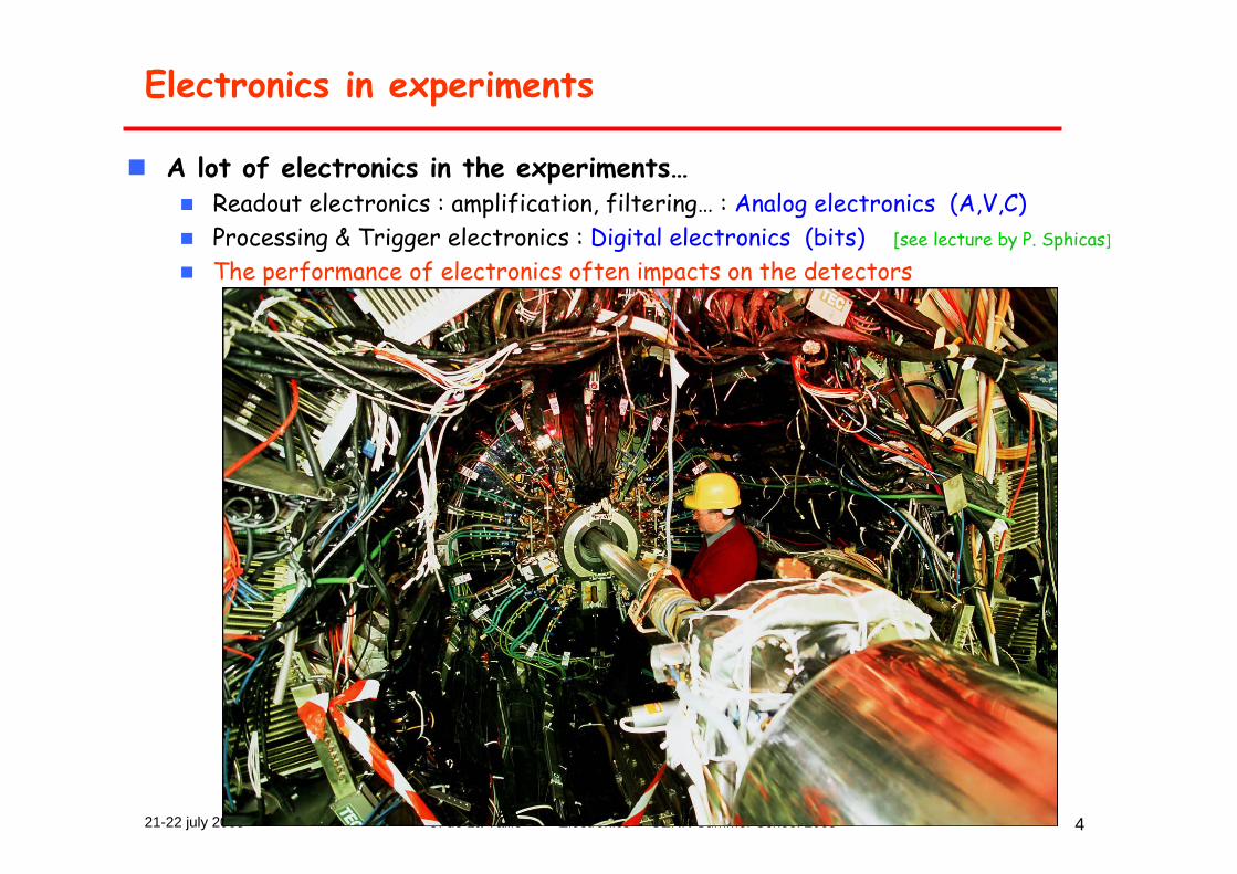
Electronics in experiments
A lot of electronics in the experiments…Readout electronics : amplification, filtering… : Analog electronics (A,V,C)Processing & Trigger electronics : Digital electronics (bits) [see lecture by P. Sphicas]
The performance of electronics often impacts on the detectors
21-22 july 2005 C. de La Taille Electronics CERN Summer School 2005 5
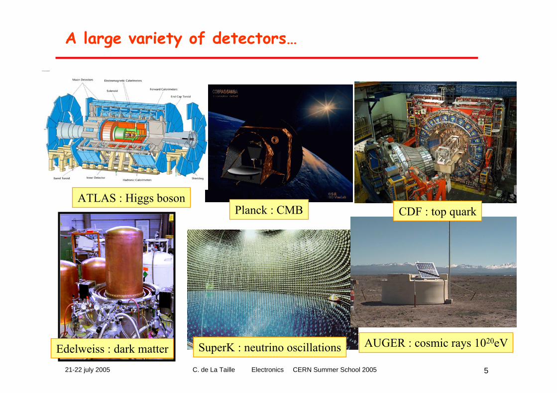
A large variety of detectors…
ATLAS : Higgs boson
SuperK : neutrino oscillations AUGER : cosmic rays 1020eV
CDF : top quarkPlanck : CMB
Edelweiss : dark matter
21-22 july 2005 C. de La Taille Electronics CERN Summer School 2005 6
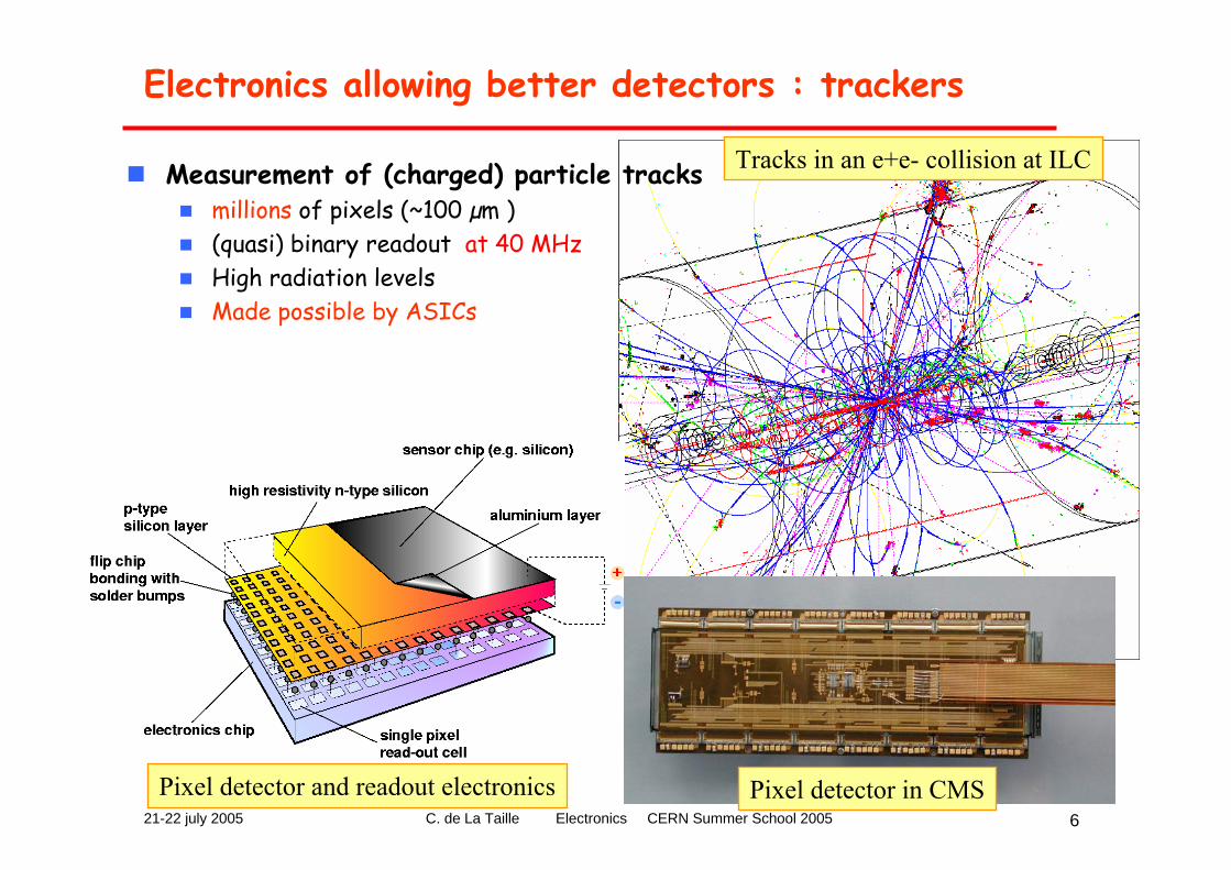
Electronics allowing better detectors : trackers
Measurement of (charged) particle tracksmillions of pixels (~100 µm )(quasi) binary readout at 40 MHzHigh radiation levelsMade possible by ASICs
Tracks in an e+e- collision at ILC
Pixel detector and readout electronics Pixel detector in CMS
21-22 july 2005 C. de La Taille Electronics CERN Summer School 2005 7
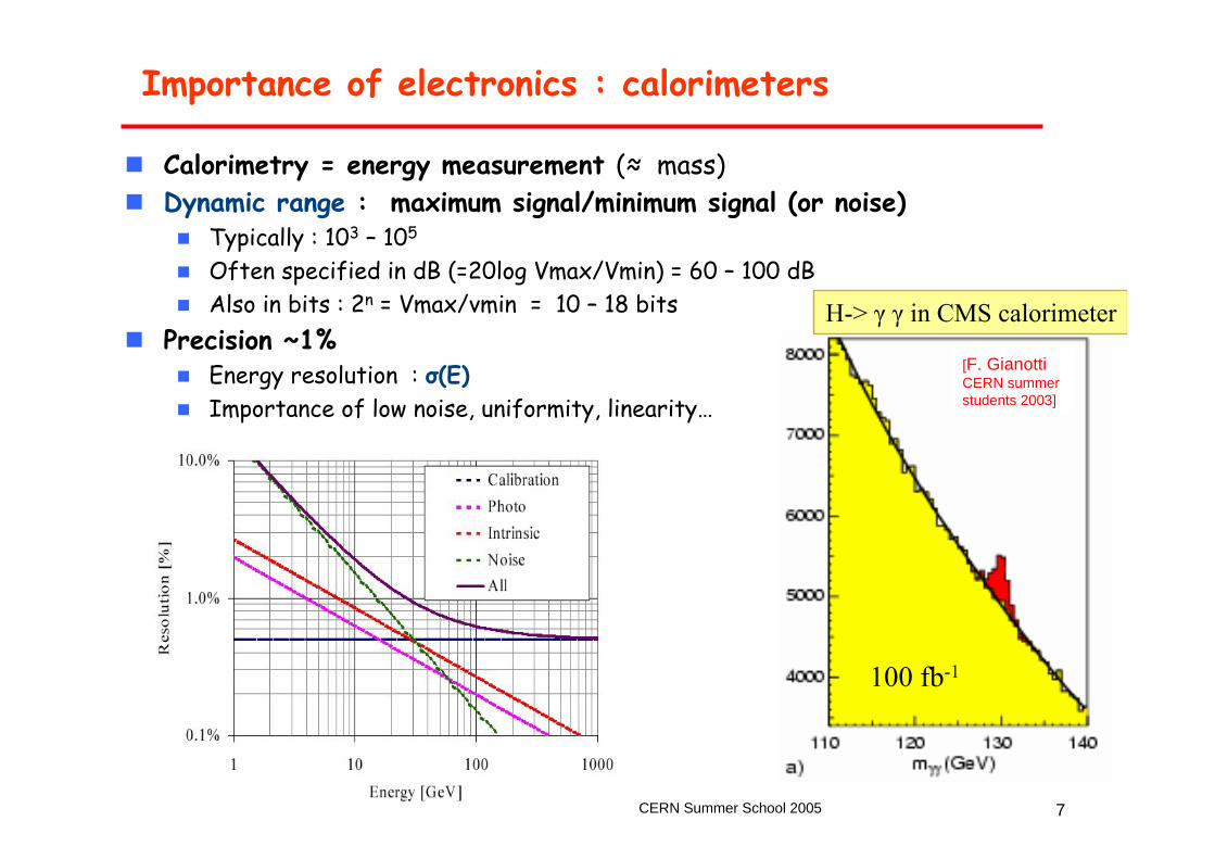
Importance of electronics : calorimeters
100 fb-1
H-> γ γ in CMS calorimeter
[F. GianottiCERN summer students 2003]
Calorimetry = energy measurement (≈ mass)Dynamic range : maximum signal/minimum signal (or noise)
Typically : 103 – 105
Often specified in dB (=20log Vmax/Vmin) = 60 – 100 dBAlso in bits : 2n = Vmax/vmin = 10 – 18 bits
Precision ~1%Energy resolution : σ(E)Importance of low noise, uniformity, linearity…

21-22 july 2005 C. de La Taille Electronics CERN Summer School 2005 8
Detector
Overview of readout electronics
Most front-ends follow a similar architecture
Preamp Shaper Analogmemory
ADC
Very small signals (fC) -> need amplificationMeasurement of amplitude and/or time (ADCs, discris, TDCs)Several thousands to millions of channels
fC V bitsFIFODSP…
V V
21-22 july 2005 C. de La Taille Electronics CERN Summer School 2005 9
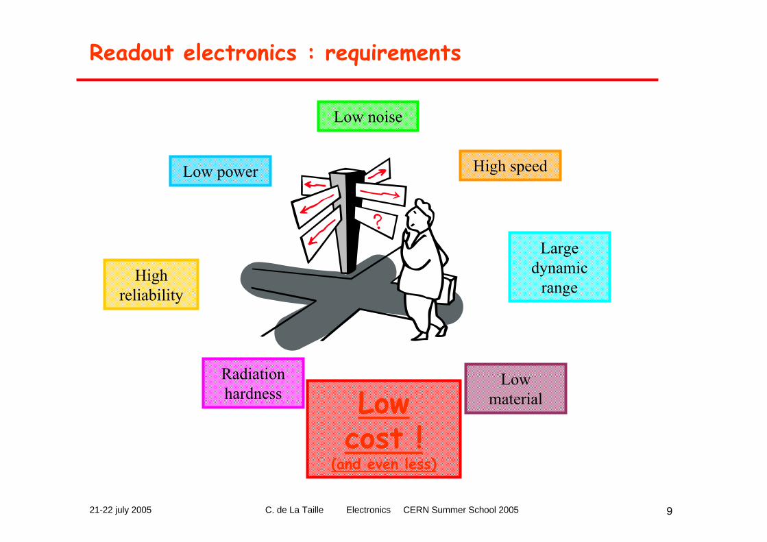
Readout electronics : requirements
Lowcost !
(and even less)
Radiation hardness
Highreliability
High speed
Large dynamic
range
Low power
Lowmaterial
Low noise
21-22 july 2005 C. de La Taille Electronics CERN Summer School 2005 10
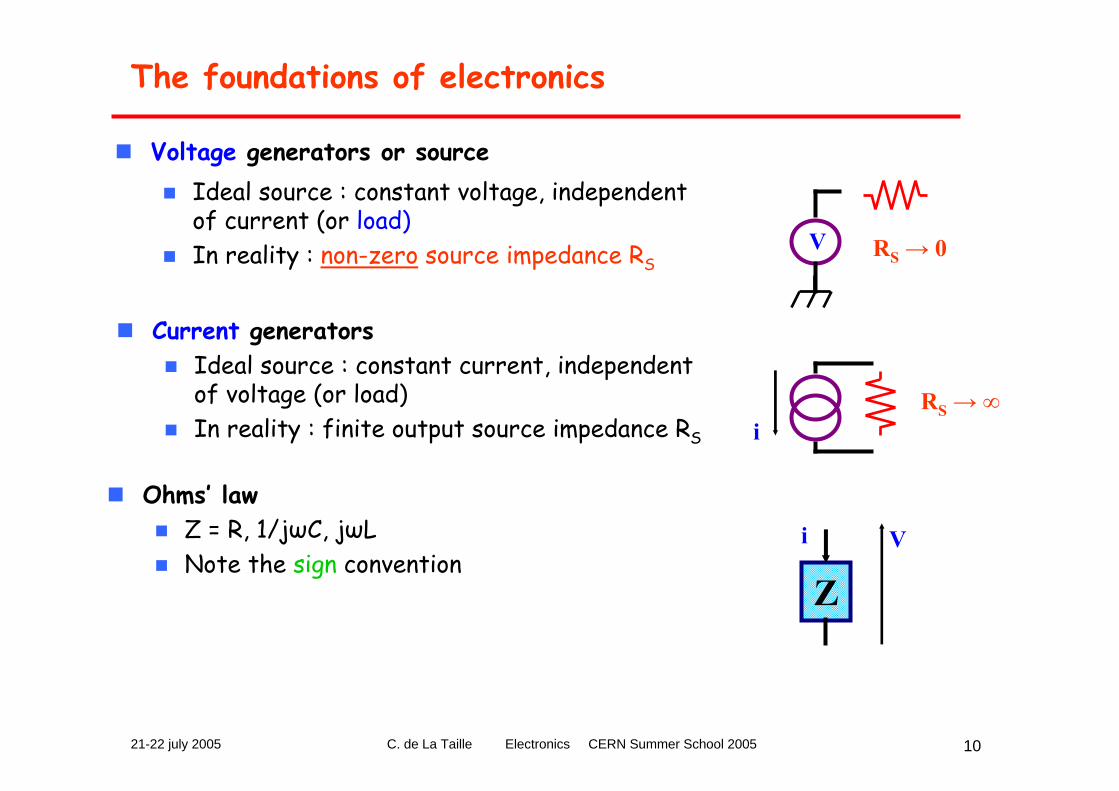
The foundations of electronics
Voltage generators or source
RS → 0
Ideal source : constant voltage, independentof current (or load)In reality : non-zero source impedance RS
Current generatorsIdeal source : constant current, independentof voltage (or load)In reality : finite output source impedance RS
Ohms’ lawZ = R, 1/jωC, jωLNote the sign convention
ZVi
V
RS →∞i
21-22 july 2005 C. de La Taille Electronics CERN Summer School 2005 11
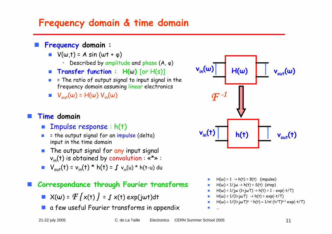
Frequency domain & time domain
Frequency domain : V(ω,t) = A sin (ωt + φ)
• Described by amplitude and phase (A, φ)Transfer function : H(ω) [or H(s)]= The ratio of output signal to input signal in thefrequency domain assuming linear electronicsVout(ω) = H(ω) Vin(ω)
Time domainImpulse response : h(t) = the output signal for an impulse (delta) input in the time domainThe output signal for any input signal vin(t) is obtained by convolution : «*» :Vout(t) = vin(t) * h(t) = ∫ vin(u) * h(t-u) du
Correspondance through Fourier transforms
X(ω) = F x(t) = ∫ x(t) exp(jωt)dta few useful Fourier transforms in appendix
H(ω)vin(ω) vout(ω)
h(t)vin(t) vout(t)
F -1
H(ω) = 1 -> h(t) = δ(t) (impulse)H(ω) = 1/jω -> h(t) = S(t) (step)H(ω) = 1/jω (1+jωT) -> h(t) = 1 - exp(-t/T)H(ω) = 1/(1+jωT) -> h(t) = exp(-t/T) H(ω) = 1/(1+jωT)n -> h(t) = 1/n! (t/T)n-1 exp(-t/T)…
21-22 july 2005 C. de La Taille Electronics CERN Summer School 2005 12
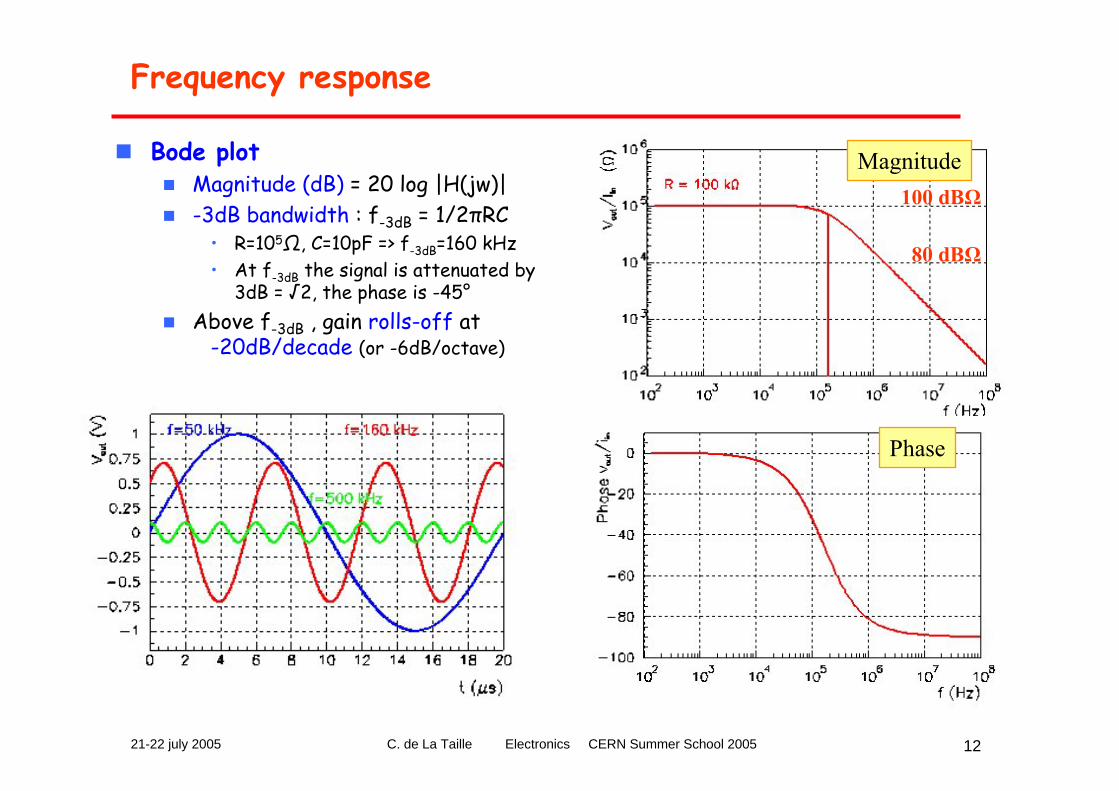
Frequency response
Bode plotMagnitude (dB) = 20 log |H(jw)|-3dB bandwidth : f-3dB = 1/2πRC
• R=105Ω, C=10pF => f-3dB=160 kHz• At f-3dB the signal is attenuated by
3dB = √2, the phase is -45°Above f-3dB , gain rolls-off at
-20dB/decade (or -6dB/octave)
100 dBΩ
80 dBΩ
Magnitude
Phase
21-22 july 2005 C. de La Taille Electronics CERN Summer School 2005 13
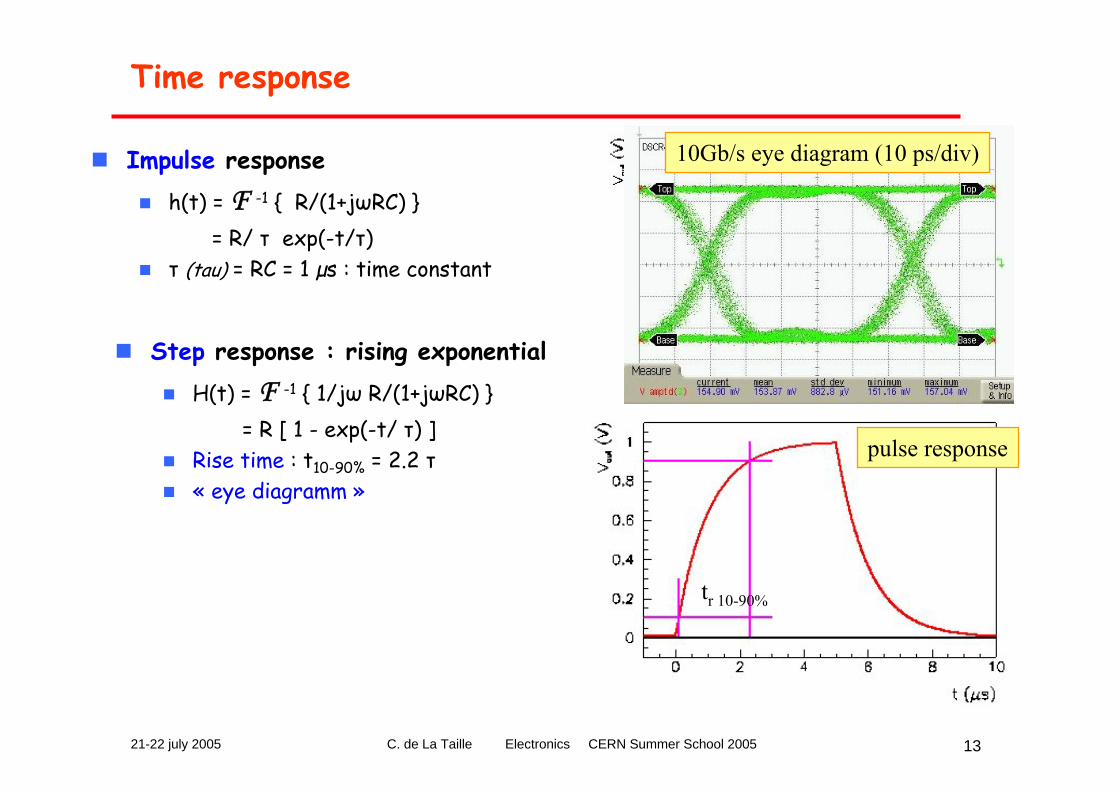
Time response
Step response : rising exponentialH(t) = F -1 1/jω R/(1+jωRC)
= R [ 1 - exp(-t/ τ) ]Rise time : t10-90% = 2.2 τ« eye diagramm »
Impulse responseh(t) = F -1 R/(1+jωRC)
= R/ τ exp(-t/τ)τ (tau) = RC = 1 µs : time constant
pulse response
tr 10-90%
Impulse response10Gb/s eye diagram (10 ps/div)
21-22 july 2005 C. de La Taille Electronics CERN Summer School 2005 14
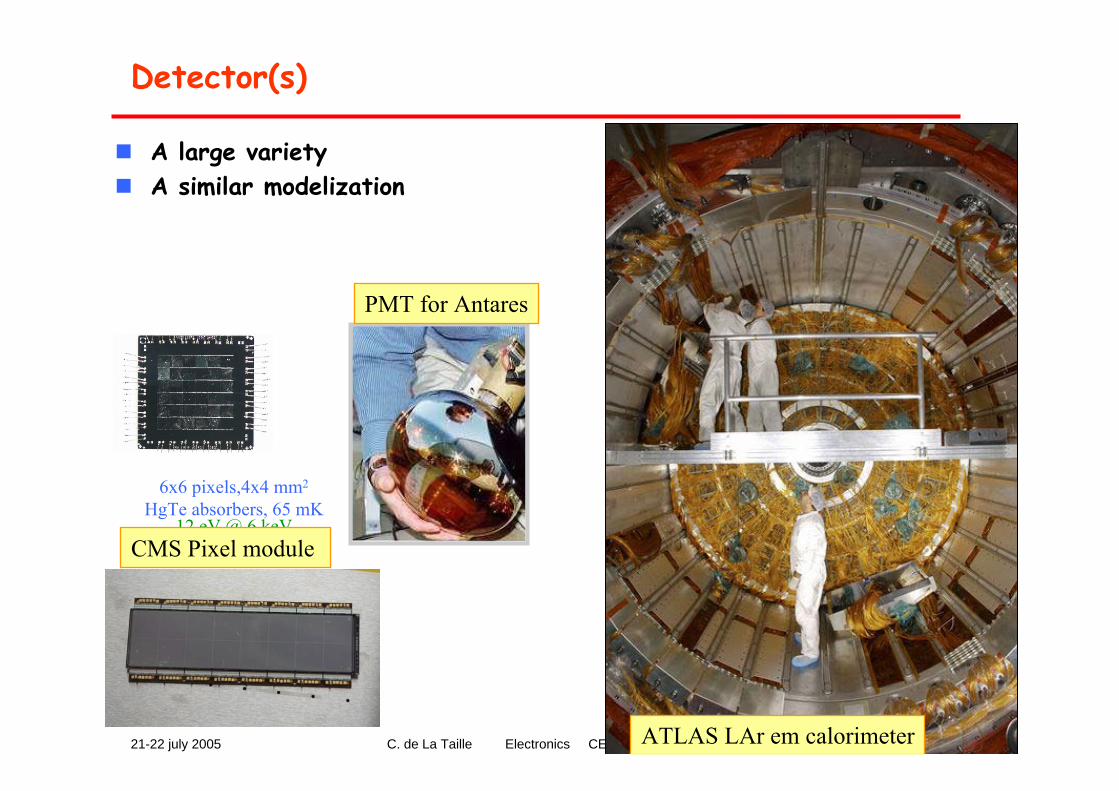
Detector(s)
A large varietyA similar modelization
6x6 pixels,4x4 mm2
HgTe absorbers, 65 mK12 eV @ 6 keV
ATLAS LAr em calorimeter
PMT for Antares
CMS Pixel module
21-22 july 2005 C. de La Taille Electronics CERN Summer School 2005 15
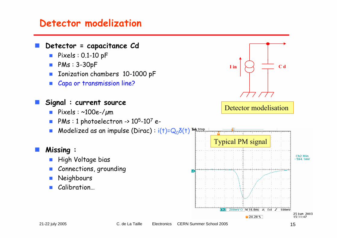
Detector modelization
Detector = capacitance CdPixels : 0.1-10 pFPMs : 3-30pFIonization chambers 10-1000 pFCapa or transmission line?
Signal : current source Pixels : ~100e-/µmPMs : 1 photoelectron -> 105-107 e-Modelized as an impulse (Dirac) : i(t)=Q0δ(t)
Missing :High Voltage biasConnections, groundingNeighboursCalibration…
I in C d
Detector modelisation
Typical PM signal
21-22 july 2005 C. de La Taille Electronics CERN Summer School 2005 16
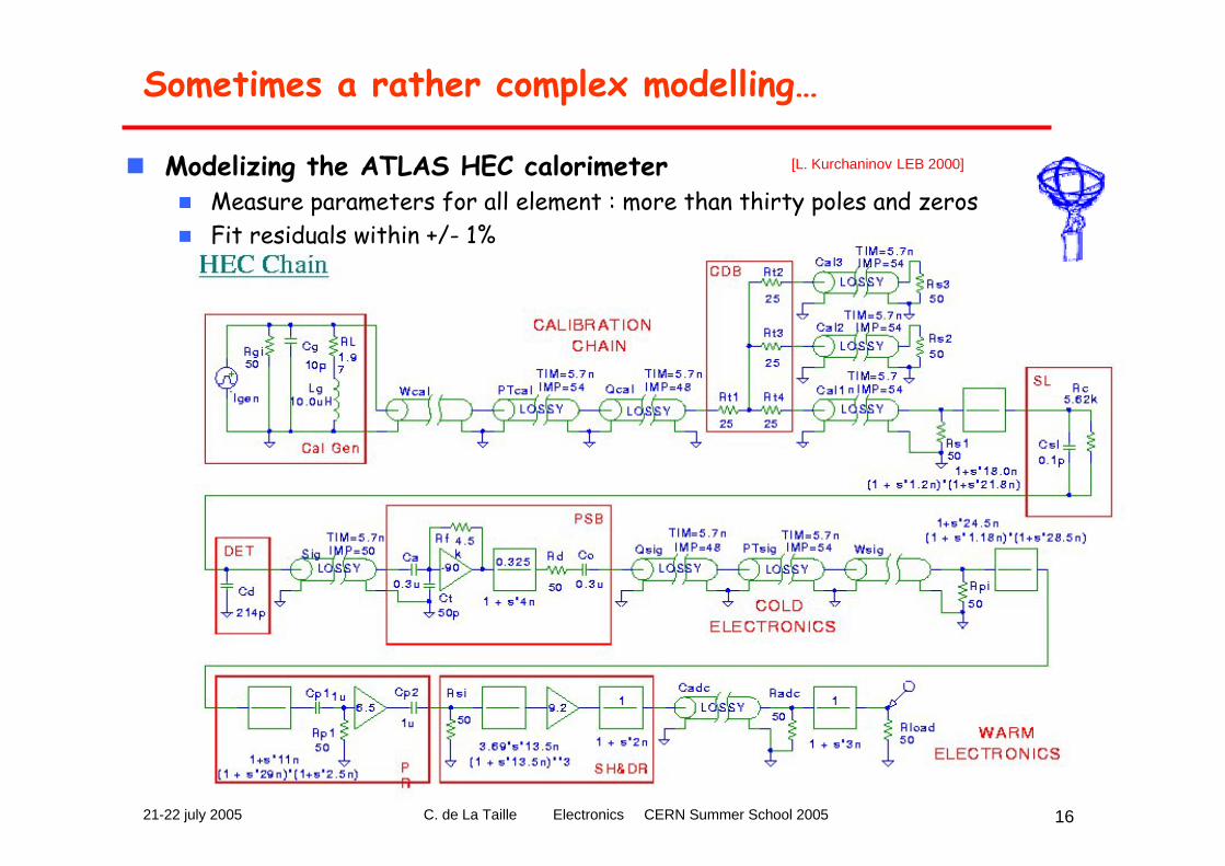
Sometimes a rather complex modelling…
Modelizing the ATLAS HEC calorimeterMeasure parameters for all element : more than thirty poles and zerosFit residuals within +/- 1%
[L. Kurchaninov LEB 2000]
21-22 july 2005 C. de La Taille Electronics CERN Summer School 2005 17
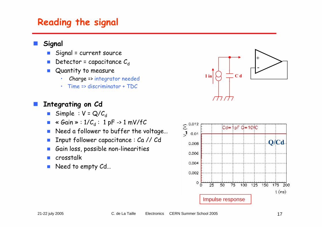
Reading the signal
Signal Signal = current source Detector = capacitance CdQuantity to measure
• Charge => integrator needed• Time => discriminator + TDC
Integrating on CdSimple : V = Q/Cd« Gain » : 1/Cd : 1 pF -> 1 mV/fCNeed a follower to buffer the voltage…Input follower capacitance : Ca // CdGain loss, possible non-linearitiescrosstalkNeed to empty Cd…
I in C d
-+
Q/Cd
Impulse response
21-22 july 2005 C. de La Taille Electronics CERN Summer School 2005 18
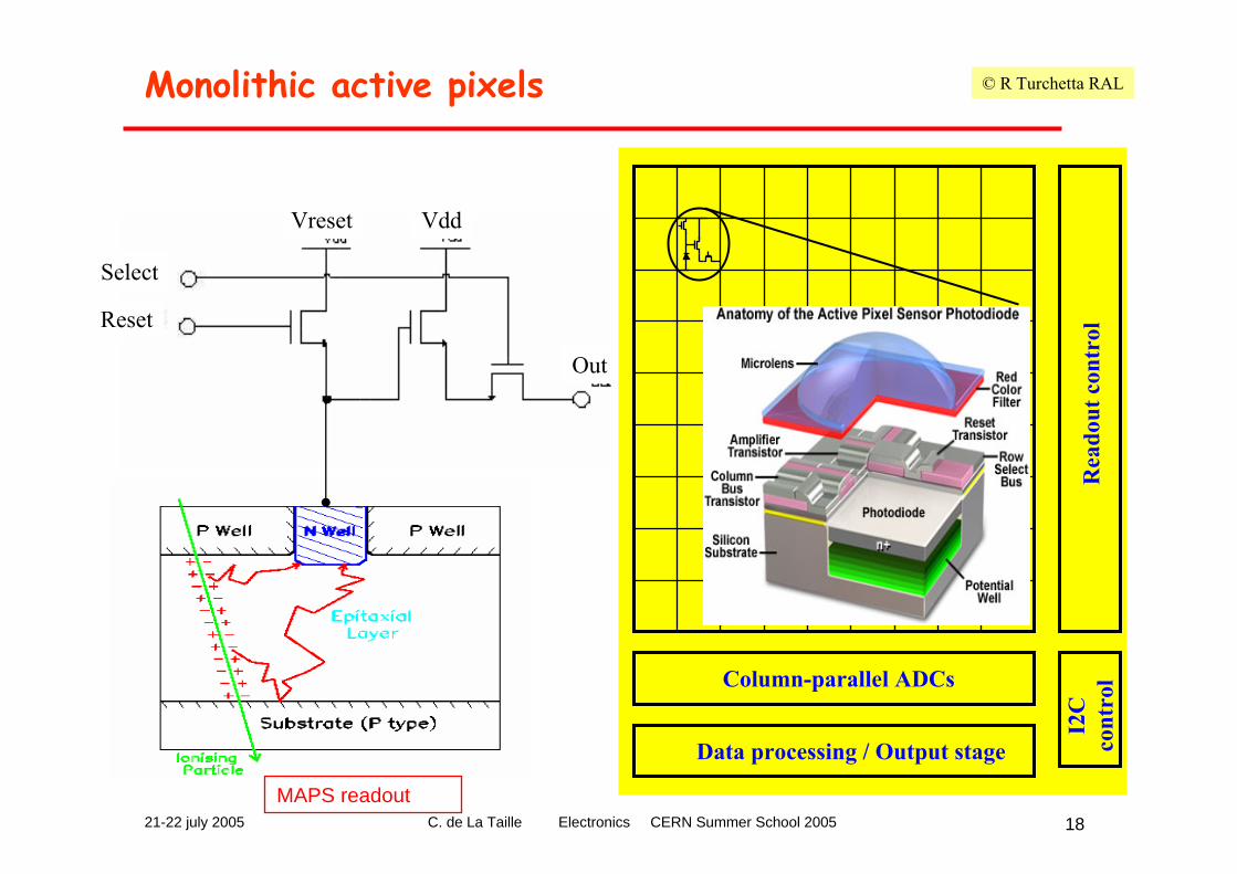
Monolithic active pixels
Epitaxial layer forms sensitive volume (2-20μm)Charge collection by diffusionCharge collected by N-well
Vreset Vdd
Out
Select
Reset
© R Turchetta RAL
Column-parallel ADCs
Data processing / Output stage
Rea
dout
con
trol
I2C
co
ntro
l
MAPS readout
21-22 july 2005 C. de La Taille Electronics CERN Summer School 2005 19
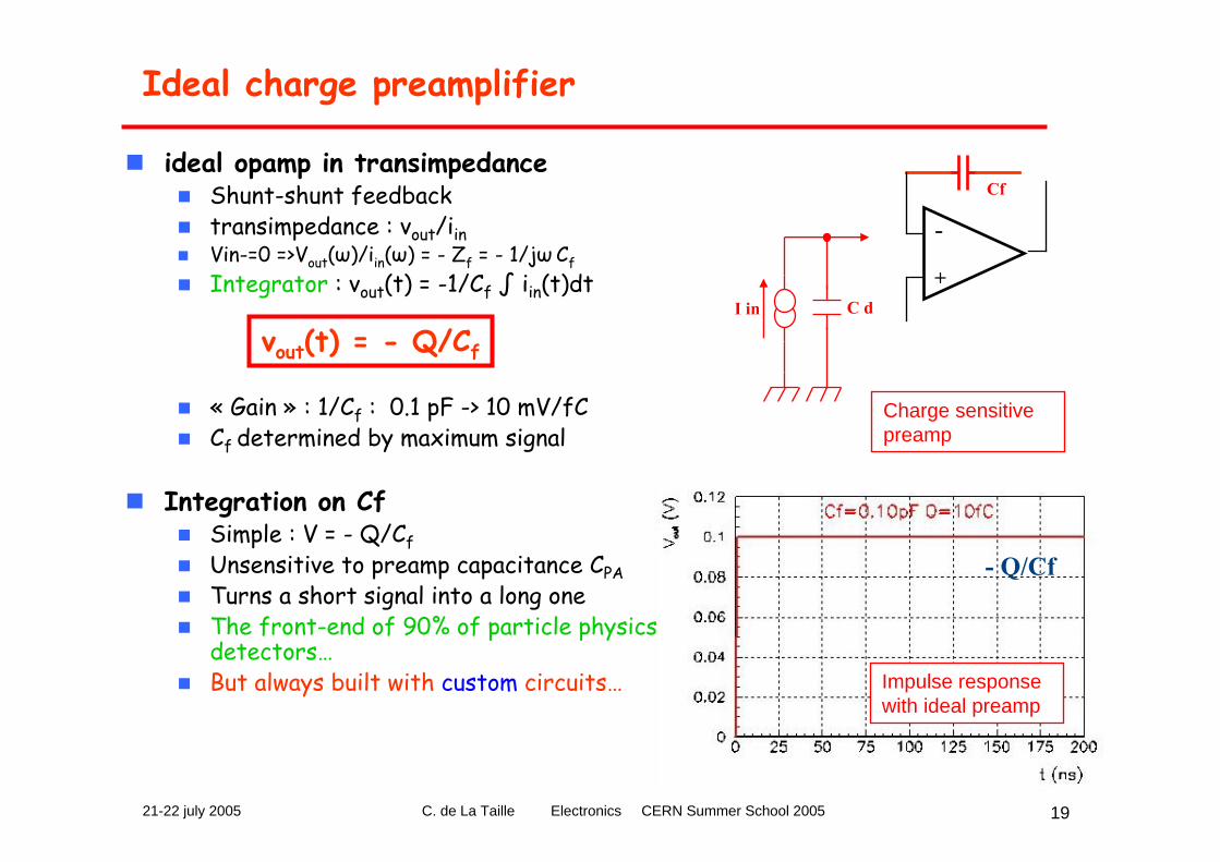
Ideal charge preamplifier
ideal opamp in transimpedanceShunt-shunt feedbacktransimpedance : vout/iinVin-=0 =>Vout(ω)/iin(ω) = - Zf = - 1/jω Cf
Integrator : vout(t) = -1/Cf ∫ iin(t)dt
« Gain » : 1/Cf : 0.1 pF -> 10 mV/fCCf determined by maximum signal
Integration on CfSimple : V = - Q/CfUnsensitive to preamp capacitance CPATurns a short signal into a long oneThe front-end of 90% of particle physicsdetectors…But always built with custom circuits…
-
+
Cf
I in C d
vout(t) = - Q/Cf
- Q/Cf
Charge sensitive preamp
Impulse responsewith ideal preamp
21-22 july 2005 C. de La Taille Electronics CERN Summer School 2005 20
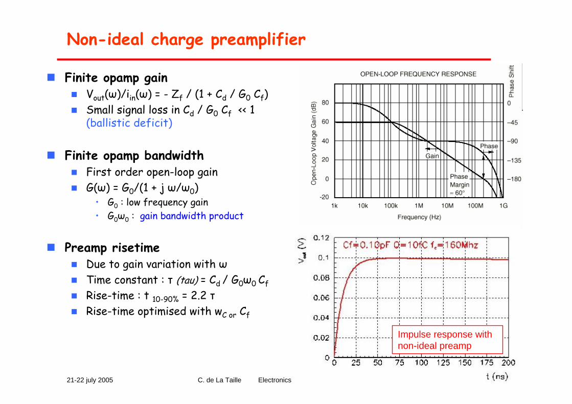
Non-ideal charge preamplifier
Finite opamp gainVout(ω)/iin(ω) = - Zf / (1 + Cd / G0 Cf)Small signal loss in Cd / G0 Cf << 1(ballistic deficit)
Finite opamp bandwidthFirst order open-loop gain G(ω) = G0/(1 + j ω/ω0)
• G0 : low frequency gain • G0ω0 : gain bandwidth product
Preamp risetimeDue to gain variation with ωTime constant : τ (tau) = Cd / G0ω0 CfRise-time : t 10-90% = 2.2 τRise-time optimised with wC or Cf
Impulse response withnon-ideal preamp
21-22 july 2005 C. de La Taille Electronics CERN Summer School 2005 21
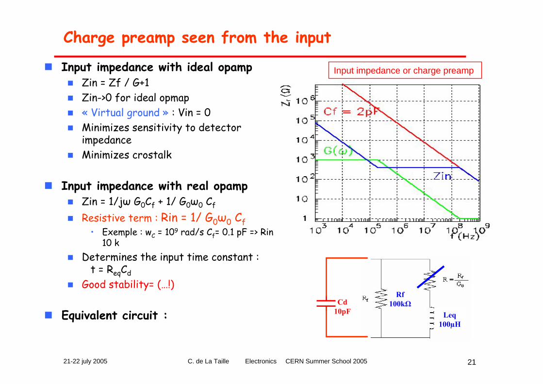
Charge preamp seen from the input
Input impedance with ideal opampZin = Zf / G+1Zin->0 for ideal opmap« Virtual ground » : Vin = 0Minimizes sensitivity to detectorimpedanceMinimizes crostalk
Input impedance with real opampZin = 1/jω G0Cf + 1/ G0ω0 Cf
Resistive term : Rin = 1/ G0ω0 Cf• Exemple : wC = 109 rad/s Cf= 0.1 pF => Rin =
10 kDetermines the input time constant :
t = ReqCdGood stability= (…!)
Equivalent circuit :Cd
10pF
Rf100kΩ
Leq100µH
Input impedance or charge preamp
21-22 july 2005 C. de La Taille Electronics CERN Summer School 2005 22
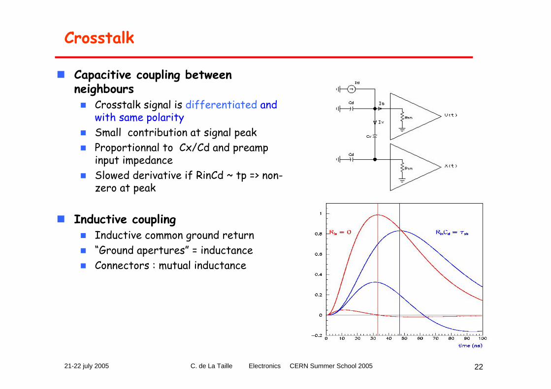
Crosstalk
Capacitive coupling between neighbours
Crosstalk signal is differentiated and with same polaritySmall contribution at signal peak Proportionnal to Cx/Cd and preamp input impedanceSlowed derivative if RinCd ~ tp => non-zero at peak
Inductive couplingInductive common ground return“Ground apertures” = inductanceConnectors : mutual inductance
21-22 july 2005 C. de La Taille Electronics CERN Summer School 2005 23
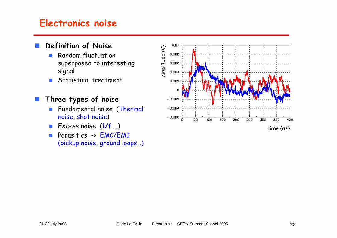
Electronics noise
Definition of NoiseRandom fluctuation superposed to interestingsignalStatistical treatment
Three types of noiseFundamental noise (Thermal noise, shot noise)Excess noise (1/f …)Parasitics -> EMC/EMI (pickup noise, ground loops…)
21-22 july 2005 C. de La Taille Electronics CERN Summer School 2005 24
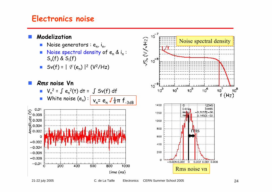
Electronics noise
ModelizationNoise generators : en, in, Noise spectral density of en & in : Sv(f) & Si(f)Sv(f) = | F (en) |2 (V2/Hz)
Rms noise VnVn
2 = ∫ en2(t) dt = ∫ Sv(f) df
White noise (en) :
rms
Rms noise vn
Noise spectral density
vn= en √½π f-3dB
21-22 july 2005 C. de La Taille Electronics CERN Summer School 2005 25
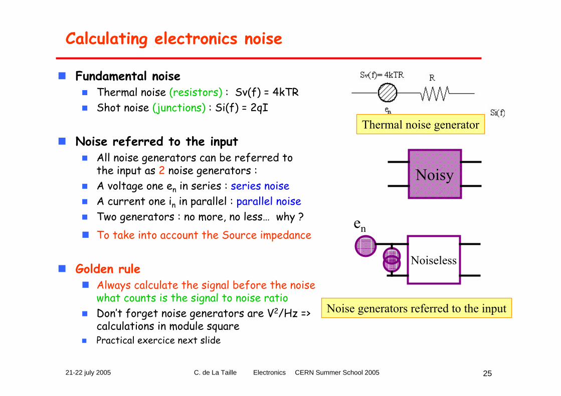
Calculating electronics noise
Fundamental noiseThermal noise (resistors) : Sv(f) = 4kTRShot noise (junctions) : Si(f) = 2qI
Noise referred to the inputAll noise generators can be referred to the input as 2 noise generators :A voltage one en in series : series noiseA current one in in parallel : parallel noiseTwo generators : no more, no less… why ?
Noisy
Noiseless
en
Thermal noise generator
Noise generators referred to the input
To take into account the Source impedance
Golden ruleAlways calculate the signal before the noise what counts is the signal to noise ratioDon’t forget noise generators are V2/Hz => calculations in module squarePractical exercice next slide
21-22 july 2005 C. de La Taille Electronics CERN Summer School 2005 26
Parallelnoise
Seriesnoise
Noise spectral densityat Preamp output
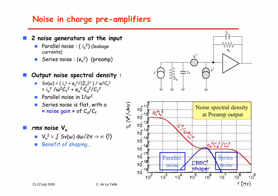
Noise in charge pre-amplifiers
2 noise generators at the inputParallel noise : ( in2) (leakagecurrents)Series noise : (en
2) (preamp)
Output noise spectral density : Sv(ω) = ( in2 + en
2/|Zd|2 ) / ω2Cf2
= in2 /ω2Cf2 + en
2 Cd2/Cf
2
Parallel noise in 1/ω2
Series noise is flat, with a « noise gain » of Cd/Cf
rms noise Vn
Vn2 = ∫ Sv(ω) dω/2π -> ∞ (!)
Benefit of shaping…
21-22 july 2005 C. de La Taille Electronics CERN Summer School 2005 27
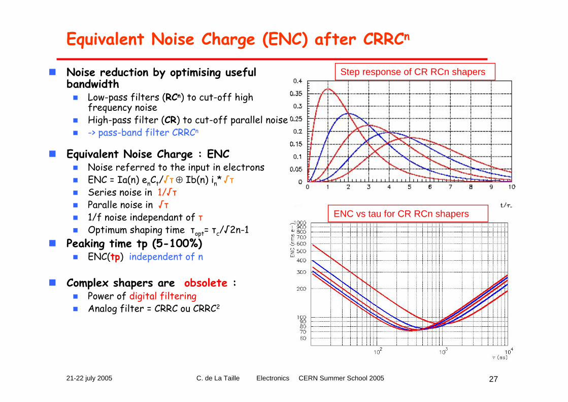
Equivalent Noise Charge (ENC) after CRRCn
Noise reduction by optimising usefulbandwidth
Low-pass filters (RCn) to cut-off highfrequency noiseHigh-pass filter (CR) to cut-off parallel noise-> pass-band filter CRRCn
Equivalent Noise Charge : ENCNoise referred to the input in electronsENC = Ia(n) enCt/√τ ⊕ Ib(n) in* √τSeries noise in 1/√τParalle noise in √τ1/f noise independant of τOptimum shaping time τopt= τc/√2n-1
Peaking time tp (5-100%)ENC(tp) independent of n
Complex shapers are obsolete :Power of digital filteringAnalog filter = CRRC ou CRRC2
Step response of CR RCn shapers
ENC vs tau for CR RCn shapers
21-22 july 2005 C. de La Taille Electronics CERN Summer School 2005 28
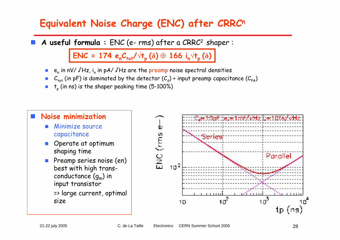
Equivalent Noise Charge (ENC) after CRRCn
A useful formula : ENC (e- rms) after a CRRC2 shaper :
en in nV/ √Hz, in in pA/ √Hz are the preamp noise spectral densitiesCtot (in pF) is dominated by the detector (Cd) + input preamp capacitance (CPA)tp (in ns) is the shaper peaking time (5-100%)
ENC = 174 enCtot/√tp (δ) ⊕ 166 in√tp (δ)
Noise minimizationMinimize source capacitanceOperate at optimum shaping timePreamp series noise (en) best with high trans-conductance (gm) in input transistor => large current, optimal size
21-22 july 2005 C. de La Taille Electronics CERN Summer School 2005 29
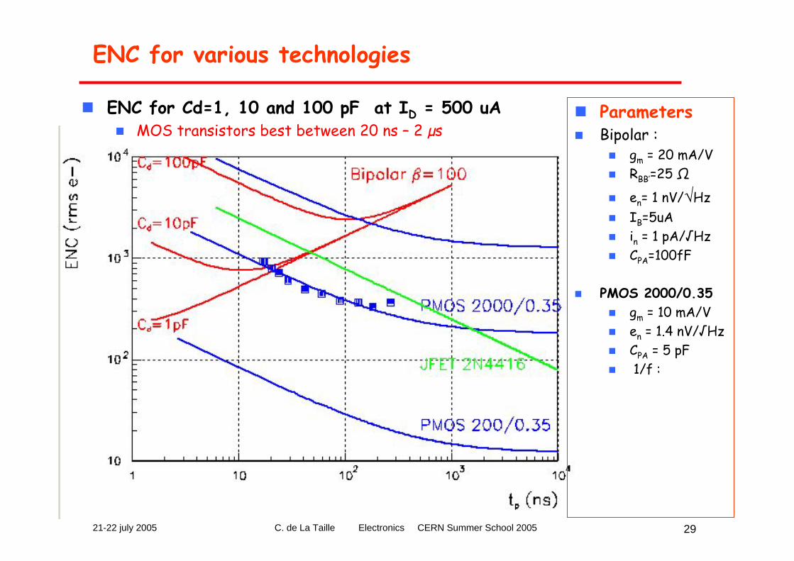
ENC for various technologies
ENC for Cd=1, 10 and 100 pF at ID = 500 uAMOS transistors best between 20 ns – 2 µs
ParametersBipolar :
gm = 20 mA/VRBB’=25 Ω
en= 1 nV/√HzIB=5uAin = 1 pA/√HzCPA=100fF
PMOS 2000/0.35gm = 10 mA/Ven = 1.4 nV/√HzCPA = 5 pF1/f :
21-22 july 2005 C. de La Taille Electronics CERN Summer School 2005 30
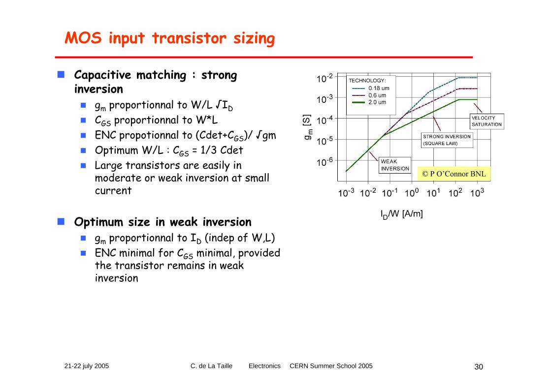
MOS input transistor sizing
Capacitive matching : strong inversion
gm proportionnal to W/L √IDCGS proportionnal to W*LENC propotionnal to (Cdet+CGS)/ √gmOptimum W/L : CGS = 1/3 CdetLarge transistors are easily in moderate or weak inversion at smallcurrent
Optimum size in weak inversiongm proportionnal to ID (indep of W,L)ENC minimal for CGS minimal, providedthe transistor remains in weakinversion
© P O’Connor BNL
21-22 july 2005 C. de La Taille Electronics CERN Summer School 2005 31
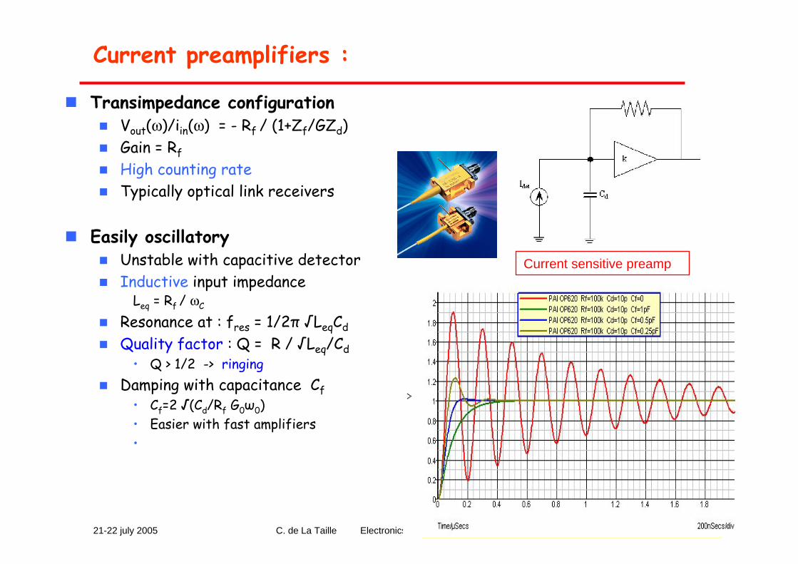
Current preamplifiers :
Transimpedance configurationVout(ω)/iin(ω) = - Rf / (1+Zf/GZd)Gain = RfHigh counting rateTypically optical link receivers
Easily oscillatoryUnstable with capacitive detectorInductive input impedance
Leq = Rf / ωC
Resonance at : fres = 1/2π √LeqCdQuality factor : Q = R / √Leq/Cd
• Q > 1/2 -> ringingDamping with capacitance Cf
• Cf=2 √(Cd/Rf G0ω0)• Easier with fast amplifiers•
Step response of current sensitive preamp
Current sensitive preamp
21-22 july 2005 C. de La Taille Electronics CERN Summer School 2005 32
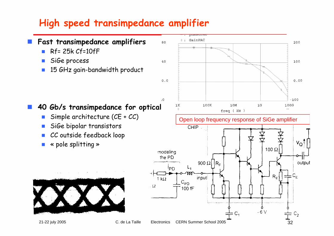
High speed transimpedance amplifier
Fast transimpedance amplifiersRf= 25k Cf=10fFSiGe process15 GHz gain-bandwidth product
40 Gb/s transimpedance for optical receiverSimple architecture (CE + CC)SiGe bipolar transistorsCC outside feedback loop« pole splitting »
Open loop frequency response of SiGe amplifier
21-22 july 2005 C. de La Taille Electronics CERN Summer School 2005 33
Course 2 : Front-end electronicsExample of design
C. de LA TAILLELAL Orsay
CERN Summer school 2005
21-22 july 2005 C. de La Taille Electronics CERN Summer School 2005 34
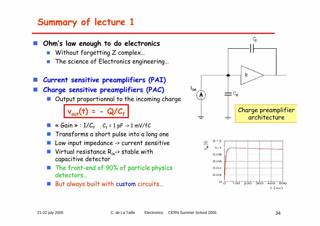
Summary of lecture 1
Charge preamplifierarchitecture
Ohm’s law enough to do electronicsWithout forgetting Z complex…The science of Electronics engineering…
Current sensitive preamplifiers (PAI)Charge sensitive preamplifiers (PAC)
Output proportionnal to the incoming charge
« Gain » : 1/Cf : Cf = 1 pF -> 1 mV/fCTransforms a short pulse into a long oneLow input impedance -> current sensitiveVirtual resistance Rin-> stable withcapacitive detectorThe front-end of 90% of particle physicsdetectors…But always built with custom circuits…
vout(t) = - Q/Cf
21-22 july 2005 C. de La Taille Electronics CERN Summer School 2005 35
Low frequency hybrid model of bipolar
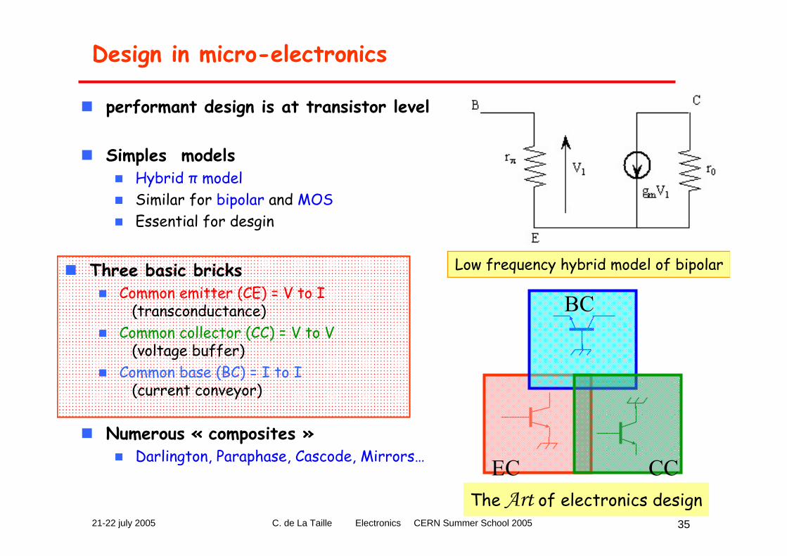
Design in micro-electronics
performant design is at transistor level
Simples modelsHybrid π modelSimilar for bipolar and MOSEssential for desgin
Numerous « composites »Darlington, Paraphase, Cascode, Mirrors…
BC
EC CCThe Art of electronics design
Three basic bricksCommon emitter (CE) = V to I
(transconductance)Common collector (CC) = V to V
(voltage buffer)Common base (BC) = I to I
(current conveyor)
21-22 july 2005 C. de La Taille Electronics CERN Summer School 2005 36
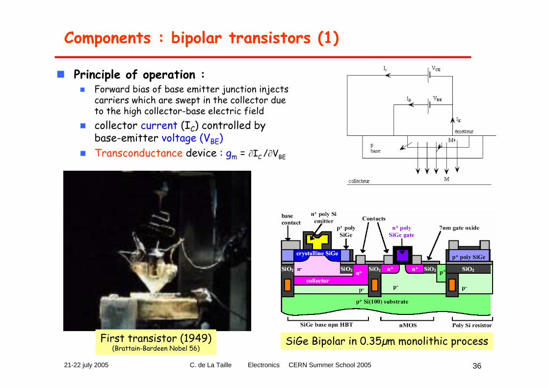
Components : bipolar transistors (1)
Principle of operation :Forward bias of base emitter junction injectscarriers which are swept in the collector due to the high collector-base electric fieldcollector current (IC) controlled by base-emitter voltage (VBE)Transconductance device : gm = ∂IC /∂VBE
First transistor (1949)(Brattain-Bardeen Nobel 56)
SiGe Bipolar in 0.35µm monolithic process
21-22 july 2005 C. de La Taille Electronics CERN Summer School 2005 37
VBE
IC
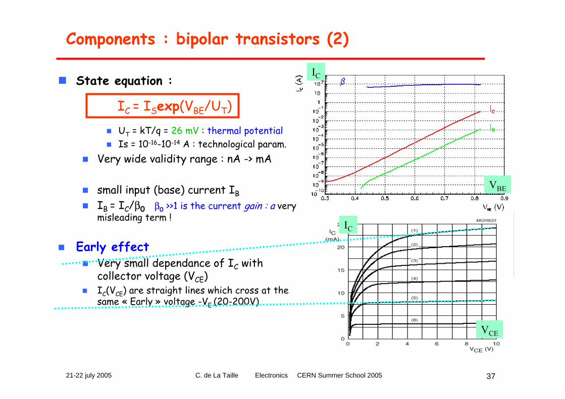
Components : bipolar transistors (2)
State equation :
UT = kT/q = 26 mV : thermal potentialIs = 10-16-10-14 A : technological param.
Very wide validity range : nA -> mA
small input (base) current IBIB = IC/β0 β0 >>1 is the current gain : a very misleading term !
Early effectVery small dependance of IC withcollector voltage (VCE) IC(VCE) are straight lines which cross at thesame « Early » voltage -VE (20-200V)
IC = ISexp(VBE/UT)
IC
VCE
21-22 july 2005 C. de La Taille Electronics CERN Summer School 2005 38
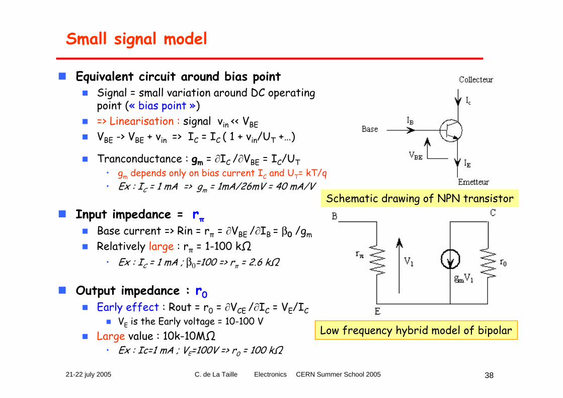
Small signal model
Equivalent circuit around bias pointSignal = small variation around DC operating point (« bias point »)=> Linearisation : signal vin << VBEVBE -> VBE + vin => IC = IC ( 1 + vin/UT +…)
Tranconductance : gm = ∂IC /∂VBE = IC/UT• gm depends only on bias current IC and UT= kT/q• Ex : IC = 1 mA => gm = 1mA/26mV = 40 mA/V
Input impedance = rπBase current => Rin = rπ = ∂VBE /∂IB = β0 /gmRelatively large : rπ = 1-100 kΩ
• Ex : IC = 1 mA ; β0=100 => rπ = 2.6 kΩ
Output impedance : r0Early effect : Rout = r0 = ∂VCE /∂IC = VE/IC
VE is the Early voltage = 10-100 VLarge value : 10k-10MΩ
• Ex : Ic=1 mA ; VE=100V => r0 = 100 kΩ
Low frequency hybrid model of bipolar
Schematic drawing of NPN transistor
21-22 july 2005 C. de La Taille Electronics CERN Summer School 2005 39
High frequency hybrid model of bipolar
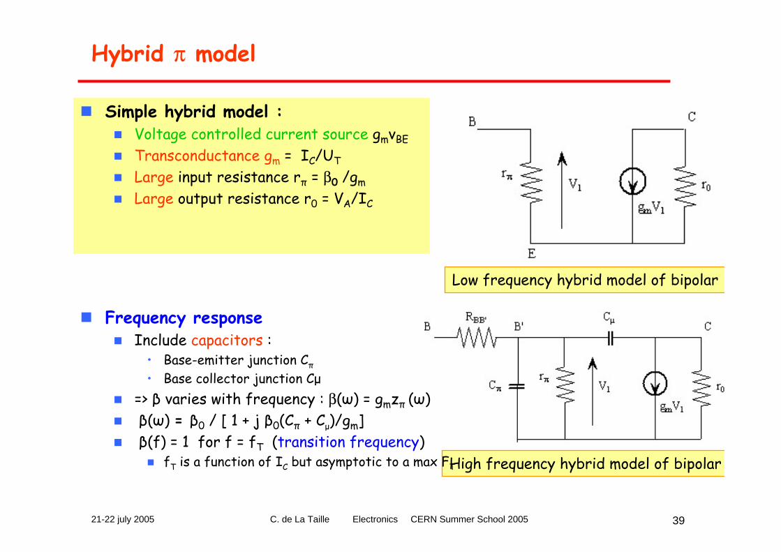
Hybrid π model
Simple hybrid model :Voltage controlled current source gmvBETransconductance gm = IC/UTLarge input resistance rπ = β0 /gmLarge output resistance r0 = VA/IC
Frequency responseInclude capacitors :
• Base-emitter junction Cπ
• Base collector junction Cμ=> β varies with frequency : β(ω) = gmzπ (ω)β(ω) = β0 / [ 1 + j β0(Cπ + Cμ)/gm]β(f) = 1 for f = fT (transition frequency)
fT is a function of IC but asymptotic to a max FT
Low frequency hybrid model of bipolar
21-22 july 2005 C. de La Taille Electronics CERN Summer School 2005 40
Components : MOS transistors
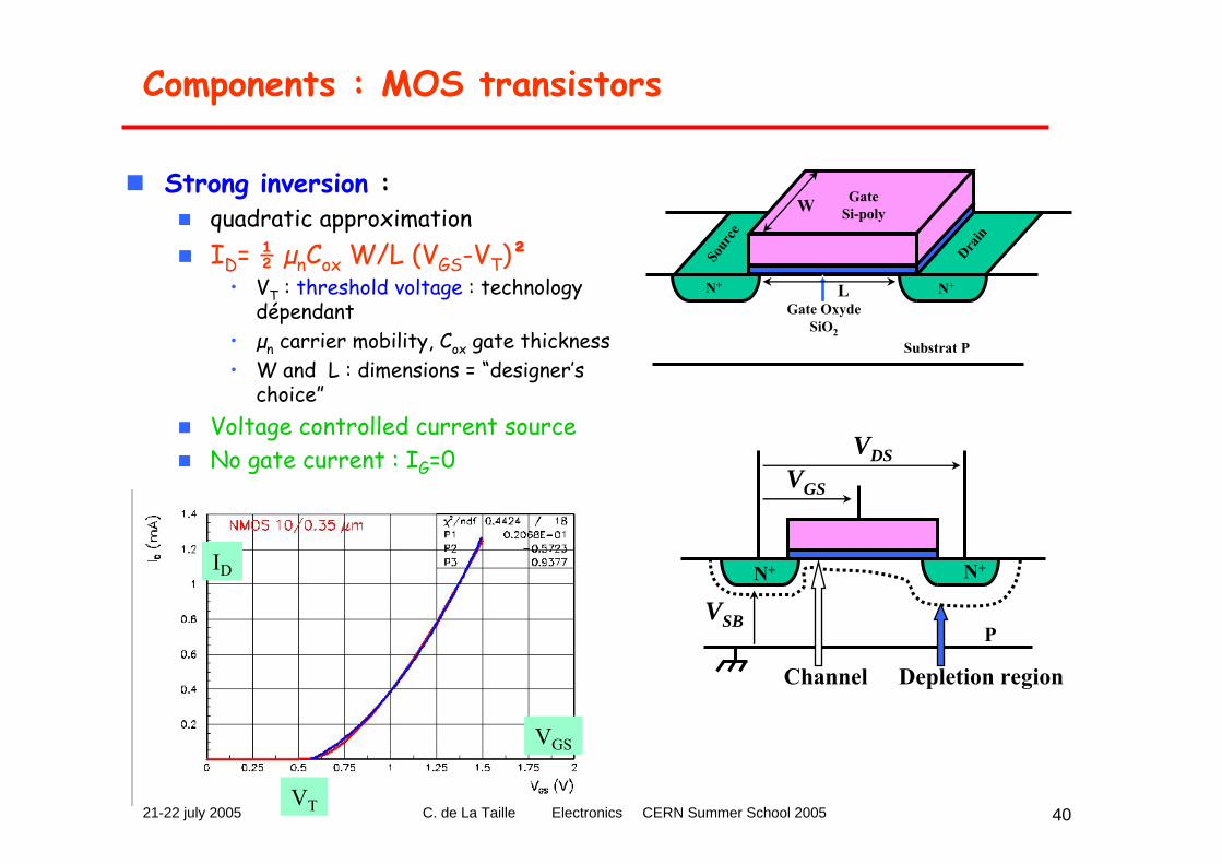
Strong inversion : quadratic approximationID= ½ µnCox W/L (VGS-VT)²
• VT : threshold voltage : technology dépendant
• µn carrier mobility, Cox gate thickness• W and L : dimensions = “designer’s
choice”Voltage controlled current sourceNo gate current : IG=0
Substrat P
Drain
Sour
ce
GateSi-poly
Gate Oxyde SiO2
N+N+
W
L
P
N+N+
VGS
VDS
VSB
Depletion regionChannel
VT
ID
VGS
21-22 july 2005 C. de La Taille Electronics CERN Summer School 2005 41
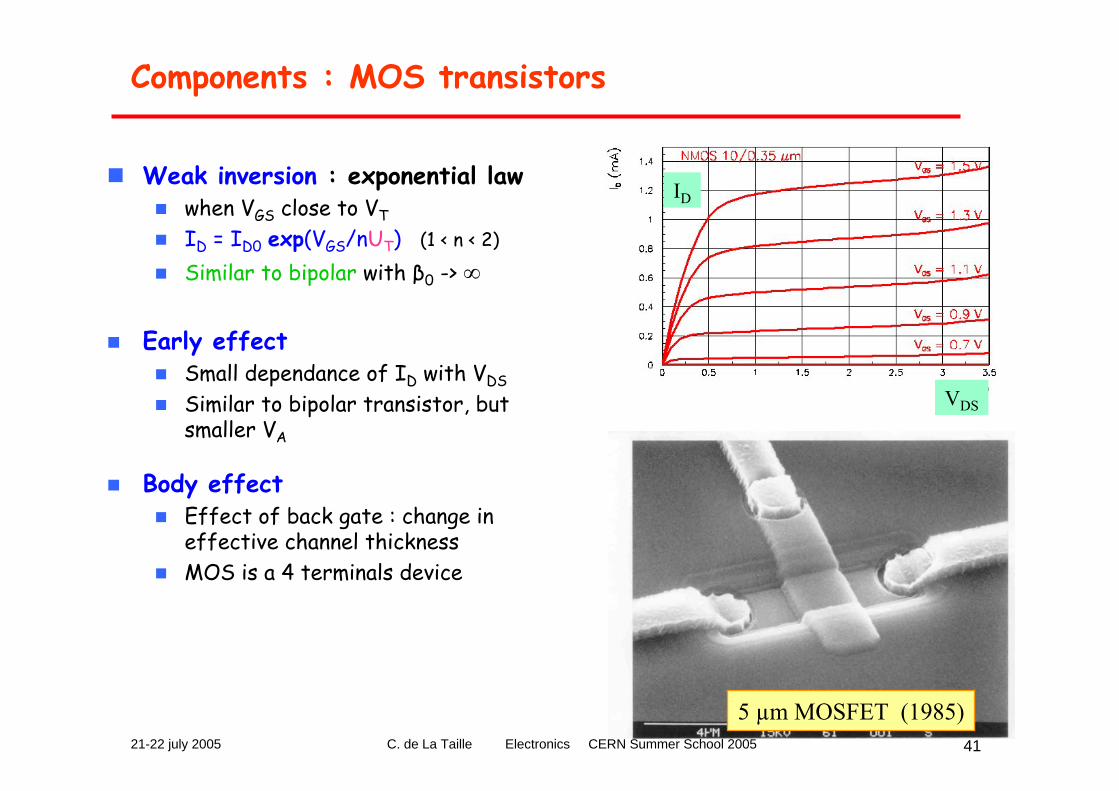
Components : MOS transistors
Weak inversion : exponential lawwhen VGS close to VTID = ID0 exp(VGS/nUT) (1 < n < 2)
Similar to bipolar with β0 -> ∞
Early effectSmall dependance of ID with VDSSimilar to bipolar transistor, but smaller VA
Body effectEffect of back gate : change in effective channel thicknessMOS is a 4 terminals device
ID
VDS
5 µm MOSFET (1985)
21-22 july 2005 C. de La Taille Electronics CERN Summer School 2005 42
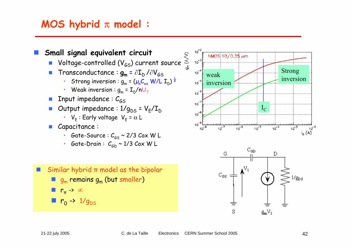
MOS hybrid π model :
Small signal equivalent circuitVoltage-controlled (VGS) current source (ID) Transconductance : gm = ∂ID /∂VGS
• Strong inversion : gm = (µnCox W/L ID) ½
• Weak inversion : gm = ID/nUT
Input impedance : CGSOutput impedance : 1/gDS = VE/ID
• VE : Early voltage VE = α LCapacitance :
• Gate-Source : CGS ~ 2/3 Cox W L• Gate-Drain : CGD ~ 1/3 Cox W L
weakinversion
Stronginversion
IC
Similar hybrid π model as the bipolargm remains gm (but smaller)rπ -> ∞r0 -> 1/gDS
21-22 july 2005 C. de La Taille Electronics CERN Summer School 2005 43
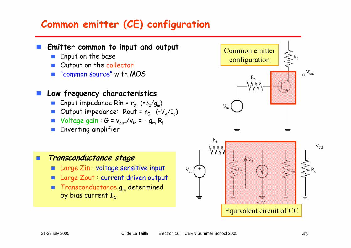
Common emitter (CE) configuration
Emitter common to input and outputInput on the baseOutput on the collector“common source” with MOS
Low frequency characteristicsInput impedance Rin = rπ (=β0/gm)Output impedance: Rout = r0 (=VA/IC)Voltage gain : G = vout/vin = - gm RLInverting amplifier
Transconductance stageLarge Zin : voltage sensitive inputLarge Zout : current driven outputTransconductance gm determined by bias current IC
Common emitterconfiguration
Equivalent circuit of CC
21-22 july 2005 C. de La Taille Electronics CERN Summer School 2005 44
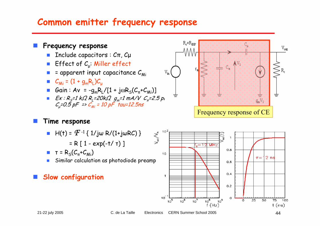
Common emitter frequency response
Frequency responseInclude capacitors : Cπ, CμEffect of Cμ: Miller effect= apparent input capacitance CMiCMi = (1 + gmRL)CμGain : Av = -gmRL/[1 + jωRS(Cπ+CMi)]Ex : RS=1 kΩ RL=20kΩ gm=1 mA/V Cπ=2.5 pFCμ=0.5 pF => CMi = 10 pF tau=12.5ns
Time responseH(t) = F -1 1/jω R/(1+jωRC)
= R [ 1 - exp(-t/ τ) ]τ = RS(Cπ+CMi) Similar calculation as photodiode preamp
Slow configuration
Frequency response of CE
21-22 july 2005 C. de La Taille Electronics CERN Summer School 2005 45
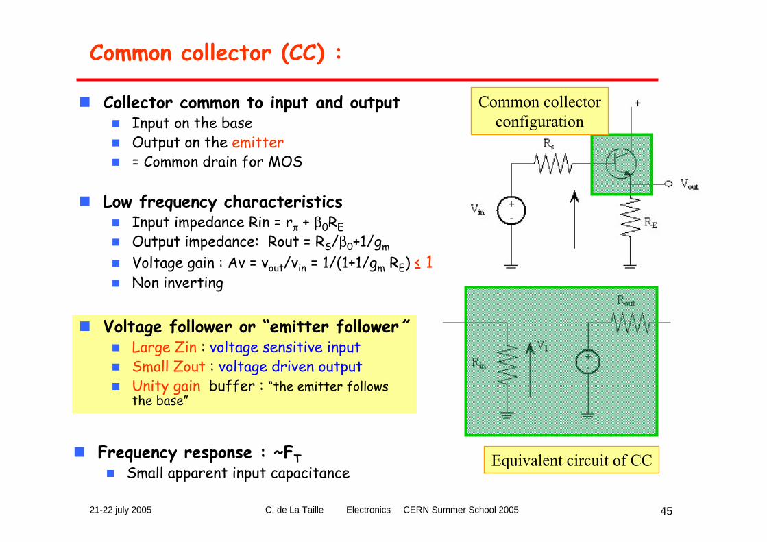
Common collector (CC) :
Collector common to input and outputInput on the baseOutput on the emitter= Common drain for MOS
Low frequency characteristicsInput impedance Rin = rπ + β0REOutput impedance: Rout = RS/β0+1/gmVoltage gain : Av = vout/vin = 1/(1+1/gm RE) ≤ 1Non inverting
Voltage follower or “emitter follower”Large Zin : voltage sensitive inputSmall Zout : voltage driven outputUnity gain buffer : “the emitter follows the base”
Frequency response : ~FTSmall apparent input capacitance
Common collectorconfiguration
Equivalent circuit of CC
21-22 july 2005 C. de La Taille Electronics CERN Summer School 2005 46
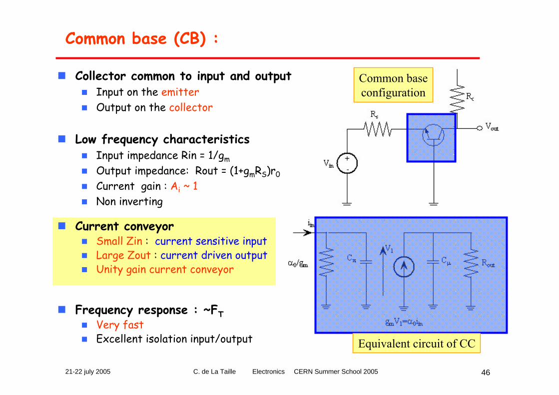
Common base (CB) :
Collector common to input and outputInput on the emitterOutput on the collector
Low frequency characteristicsInput impedance Rin = 1/gmOutput impedance: Rout = (1+gmRS)r0Current gain : Ai ~ 1Non inverting
Current conveyorSmall Zin : current sensitive inputLarge Zout : current driven outputUnity gain current conveyor
Frequency response : ~FTVery fastExcellent isolation input/output
Common baseconfiguration
Equivalent circuit of CC
21-22 july 2005 C. de La Taille Electronics CERN Summer School 2005 47
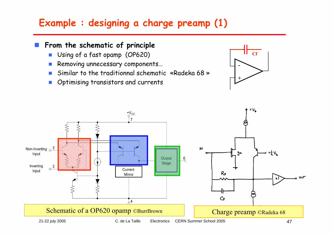
Example : designing a charge preamp (1)
From the schematic of principleUsing of a fast opamp (OP620)Removing unnecessary components…Similar to the traditionnal schematic «Radeka 68 »Optimising transistors and currents
-
+
Cf
Schematic of a OP620 opamp ©BurrBrown Charge preamp ©Radeka 68
21-22 july 2005 C. de La Taille Electronics CERN Summer School 2005 48
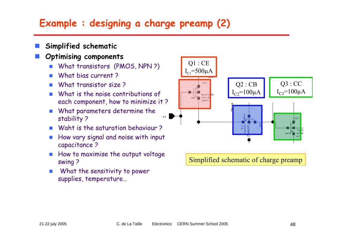
Example : designing a charge preamp (2)
Q2 : CBIC2=100µA
Q3 : CCIC3=100µA
Q1 : CEIC1=500µA
Simplified schematic of charge preamp
Simplified schematicOptimising components
What transistors (PMOS, NPN ?)What bias current ?What transistor size ?What is the noise contributions ofeach component, how to minimize it ?What parameters determine thestability ?Waht is the saturation behaviour ?How vary signal and noise with input capacitance ?How to maximise the output voltage swing ?What the sensitivity to powersupplies, temperature…
21-22 july 2005 C. de La Taille Electronics CERN Summer School 2005 49
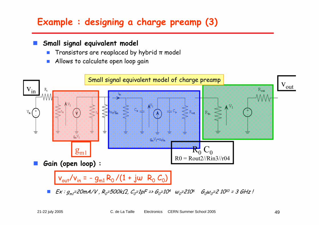
Example : designing a charge preamp (3)
Small signal equivalent modelTransistors are reaplaced by hybrid π modelAllows to calculate open loop gain
gm1
Gain (open loop) :
Ex : gm1=20mA/V , R0=500kΩ, C0=1pF => G0=104 ω0=2106 G0ω0=2 1010 = 3 GHz !
vout/vin = - gm1 R0 /(1 + jω R0 C0)
vinvout
R0 C0R0 = Rout2//Rin3//r04
Small signal equivalent model of charge preamp
21-22 july 2005 C. de La Taille Electronics CERN Summer School 2005 50
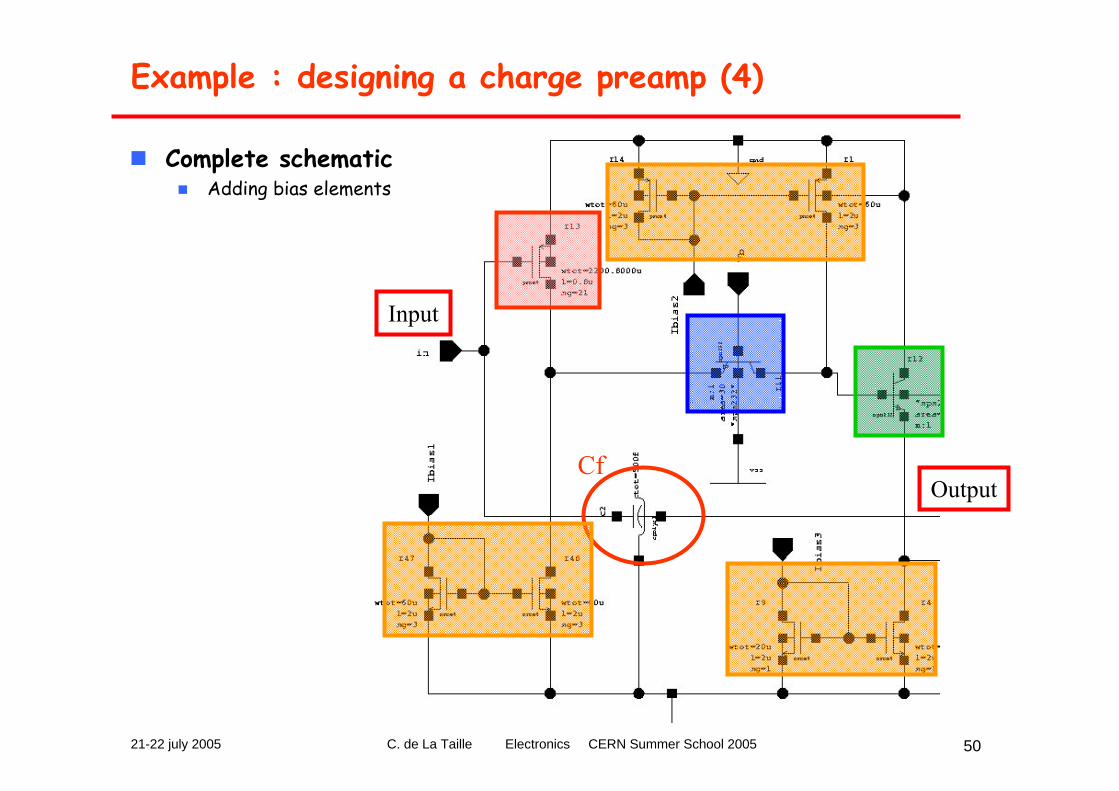
Example : designing a charge preamp (4)
Cf
Input
Output
Complete schematicAdding bias elements
21-22 july 2005 C. de La Taille Electronics CERN Summer School 2005 51
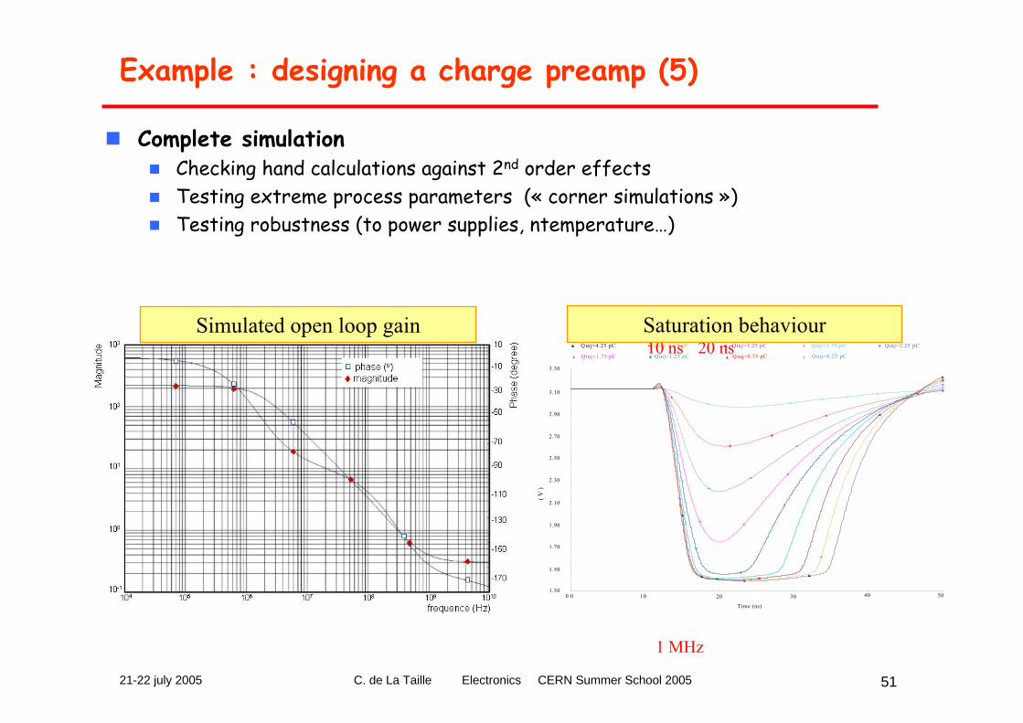
Example : designing a charge preamp (5)
Complete simulation Checking hand calculations against 2nd order effectsTesting extreme process parameters (« corner simulations »)Testing robustness (to power supplies, ntemperature…)
( V )
1.50
1.30
1.70
1.90
2.10
2.30
2.50
2.70
2.90
3.10
3.30
0.0 10 20 30 40 50
Time (ns)
Qinj=4.25 pC
Qinj=1.75 pC
Qinj=3.75 pC
Qinj=1.25 pC
Qinj=3.25 pC
Qinj=0.75 pC
Qinj=2.75 pC
Qinj=0.25 pC
Qinj=2.25 pC
1 MHz
10 ns 20 nsSimulated open loop gain Saturation behaviour
21-22 july 2005 C. de La Taille Electronics CERN Summer School 2005 52
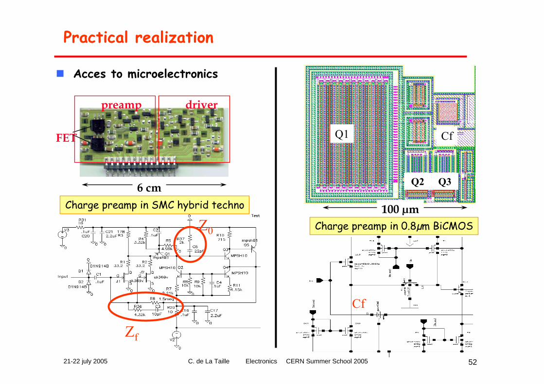
Practical realization
Acces to microelectronics
6 cm
FET
driverpreamp
100 µm
Zf
Z0
Q2
CfQ1
Q3
Cf
Charge preamp in 0.8µm BiCMOS
Charge preamp in SMC hybrid techno
21-22 july 2005 C. de La Taille Electronics CERN Summer School 2005 53
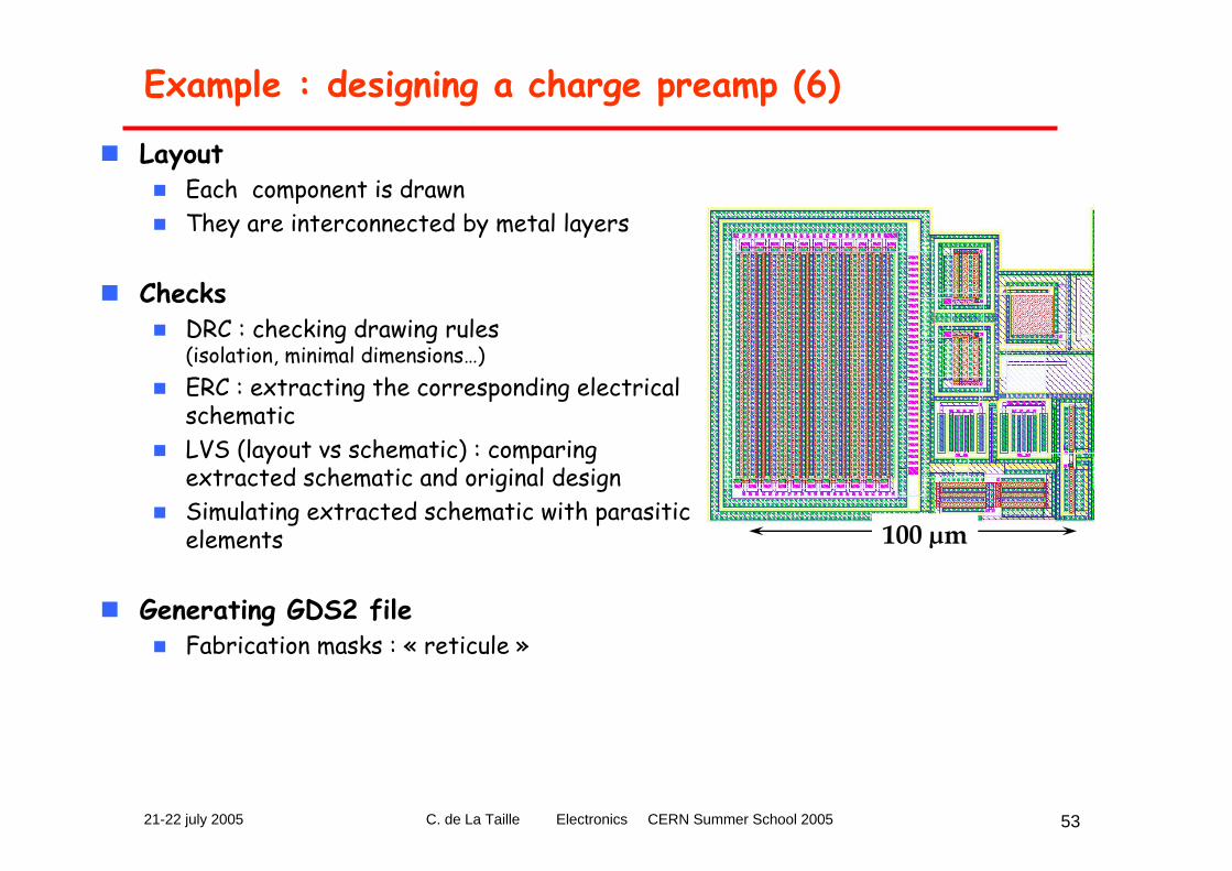
Example : designing a charge preamp (6)
LayoutEach component is drawnThey are interconnected by metal layers
ChecksDRC : checking drawing rules(isolation, minimal dimensions…)ERC : extracting the corresponding electricalschematicLVS (layout vs schematic) : comparingextracted schematic and original designSimulating extracted schematic with parasiticelements
Generating GDS2 fileFabrication masks : « reticule »
100 µm
21-22 july 2005 C. de La Taille Electronics CERN Summer School 2005 54
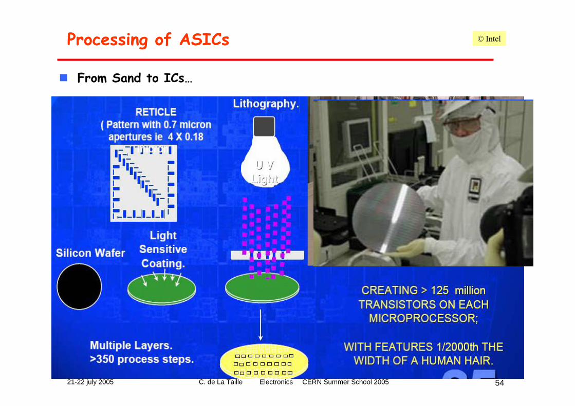
Processing of ASICs
From Sand to ICs…
© Intel
21-22 july 2005 C. de La Taille Electronics CERN Summer School 2005 55
Course 3 : Electronics in High Energy physics, evolution of technologies and
examples
C. de LA TAILLELAL Orsay
CERN Summer school 2005
21-22 july 2005 C. de La Taille Electronics CERN Summer School 2005 56
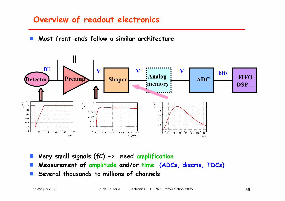
Detector
Overview of readout electronics
Most front-ends follow a similar architecture
Preamp Shaper Analogmemory
ADC
Very small signals (fC) -> need amplificationMeasurement of amplitude and/or time (ADCs, discris, TDCs)Several thousands to millions of channels
fC V bitsFIFODSP…
V V
21-22 july 2005 C. de La Taille Electronics CERN Summer School 2005 57
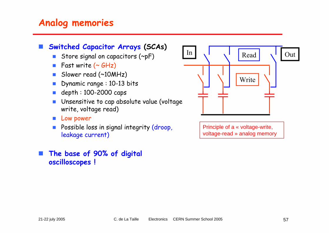
Analog memories
Switched Capacitor Arrays (SCAs)Store signal on capacitors (~pF) Fast write (~ GHz)Slower read (~10MHz)Dynamic range : 10-13 bitsdepth : 100-2000 capsUnsensitive to cap absolute value (voltage write, voltage read)Low powerPossible loss in signal integrity (droop, leakage current)
The base of 90% of digital oscilloscopes !
In
Write
Read Out
Principle of a « voltage-write, voltage-read » analog memory
21-22 july 2005 C. de La Taille Electronics CERN Summer School 2005 58
Example : SAM for HESS2
Swift Analog Memory3 Gsample/s >10 bits
serial link for configuration set-up+
16 delays / colum
d
d
d
d
q
q
d
d
d
d
q
q
d
d
d
d
q
q
d
d
d
d
q
q
d
d
d
d
q
q
Phase comparator
+ Charge Pump
Buffers
In +In -
16 columnswck
wck
2 ns pulse in SAM0
chip layout in 0.35µ CMOS
©E. Delagnes
21-22 july 2005 C. de La Taille Electronics CERN Summer School 2005 59
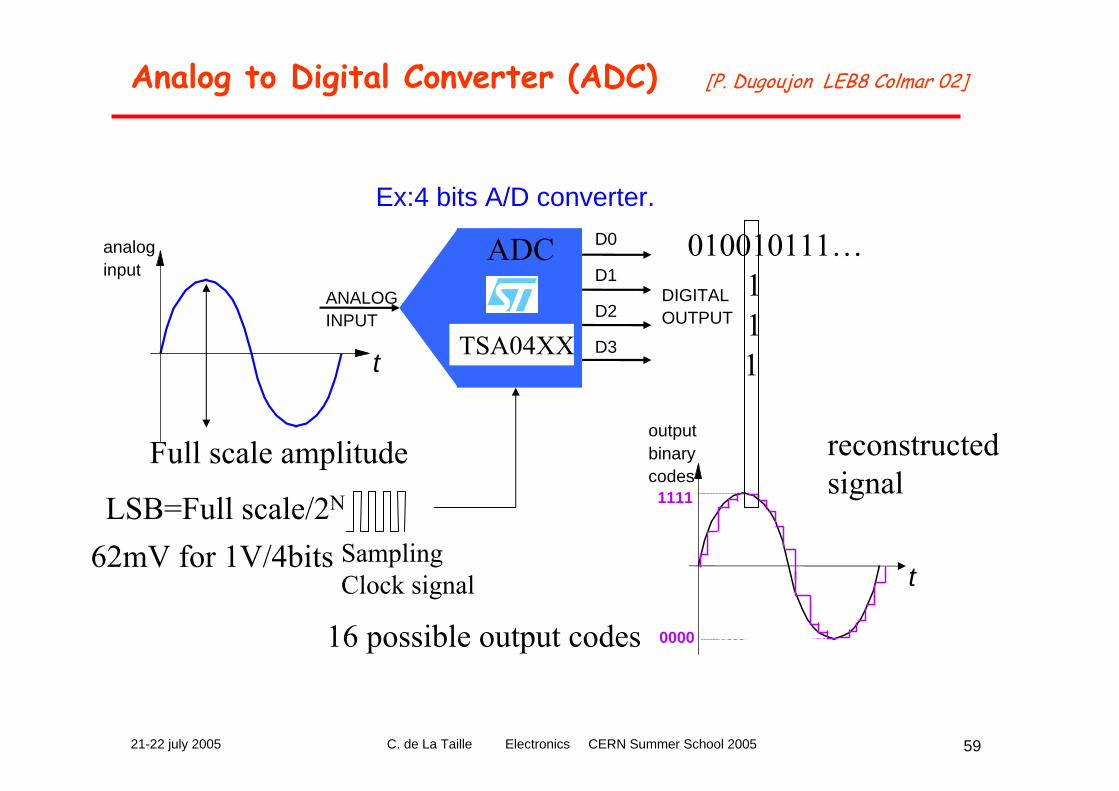
Analog to Digital Converter (ADC) [P. Dugoujon LEB8 Colmar 02]
ANALOGINPUT
D0
D3
D2
D1DIGITALOUTPUT
Ex:4 bits A/D converter.
t
analoginput
SamplingClock signal
TSA04XX
0000
1111
outputbinarycodes
reconstructedsignal
t
010010111…
1
11
16 possible output codes
ADC
Full scale amplitude
LSB=Full scale/2N
62mV for 1V/4bits
21-22 july 2005 C. de La Taille Electronics CERN Summer School 2005 60
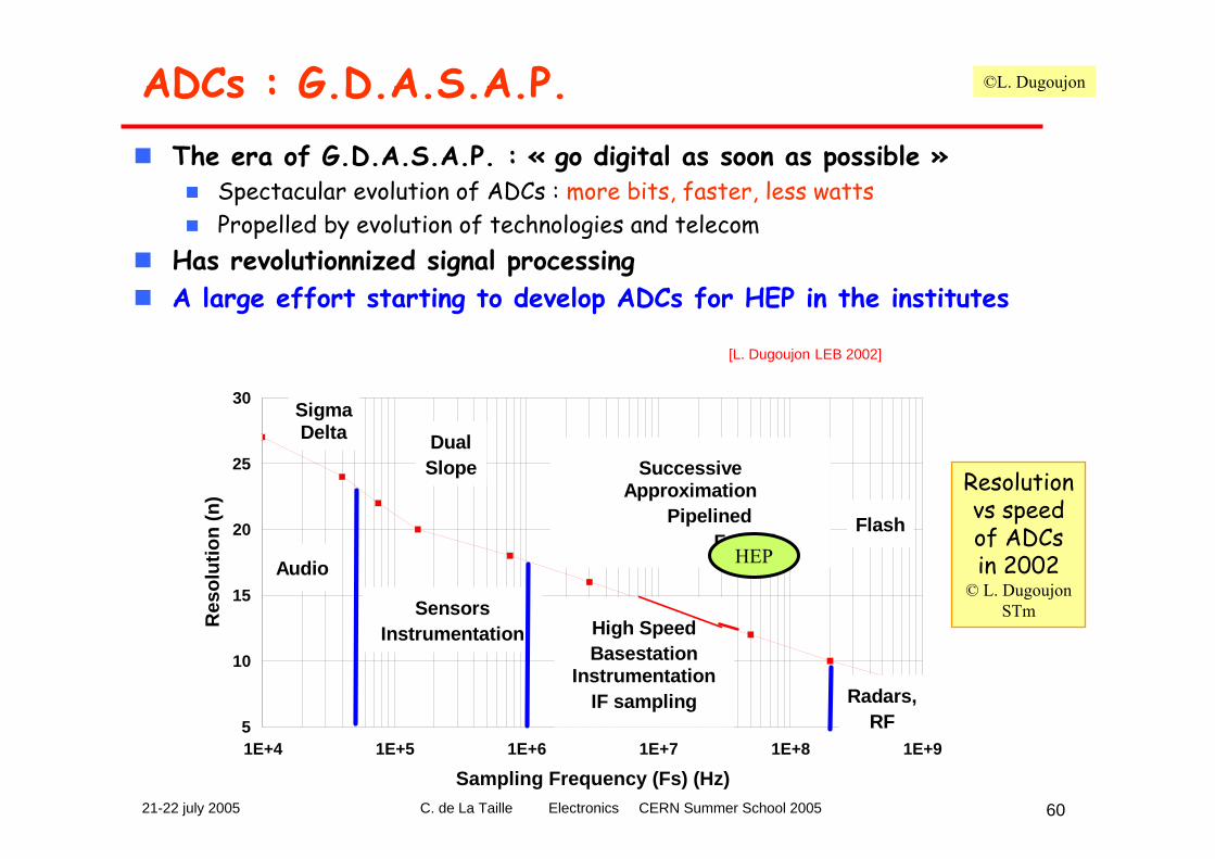
ADCs : G.D.A.S.A.P.The era of G.D.A.S.A.P. : « go digital as soon as possible »
Spectacular evolution of ADCs : more bits, faster, less wattsPropelled by evolution of technologies and telecom
Has revolutionnized signal processingA large effort starting to develop ADCs for HEP in the institutes
1E+4 1E+5 1E+6 1E+7 1E+8 1E+9
Sampling Frequency (Fs) (Hz)
5
10
15
20
25
30
Res
olut
ion
(n)
Sigma Delta Dual
Slope
Audio
SensorsInstrumentation
Successive Approximation Pipelined
Folded
High SpeedBasestation
InstrumentationIF sampling
Flash
Radars,RF
HEP
Resolution vs speed of ADCs in 2002
© L. DugoujonSTm
[L. Dugoujon LEB 2002]
©L. Dugoujon
21-22 july 2005 C. de La Taille Electronics CERN Summer School 2005 61
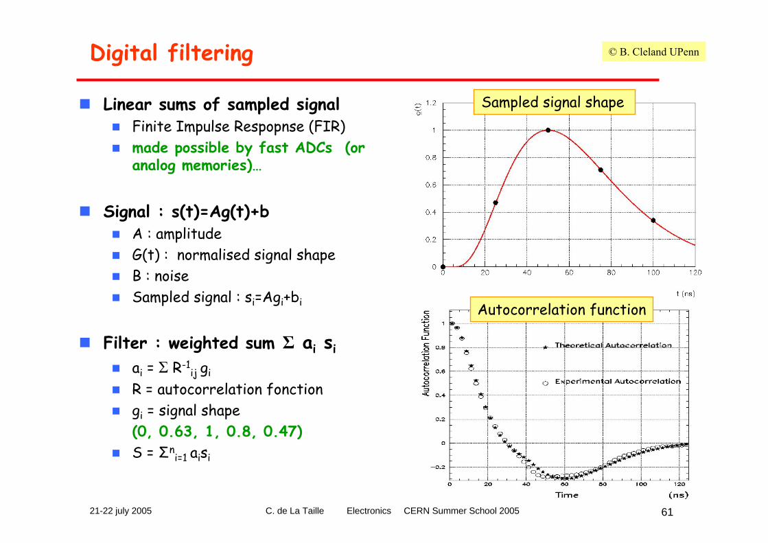
Digital filtering
Linear sums of sampled signalFinite Impulse Respopnse (FIR)made possible by fast ADCs (or analog memories)…
Signal : s(t)=Ag(t)+bA : amplitudeG(t) : normalised signal shapeB : noiseSampled signal : si=Agi+bi
Filter : weighted sum Σ ai siai = Σ R-1
ij gi
R = autocorrelation fonctiongi = signal shape (0, 0.63, 1, 0.8, 0.47)S = Σn
i=1 aisi
© B. Cleland UPenn
Sampled signal shape
Autocorrelation function
21-22 july 2005 C. de La Taille Electronics CERN Summer School 2005 62
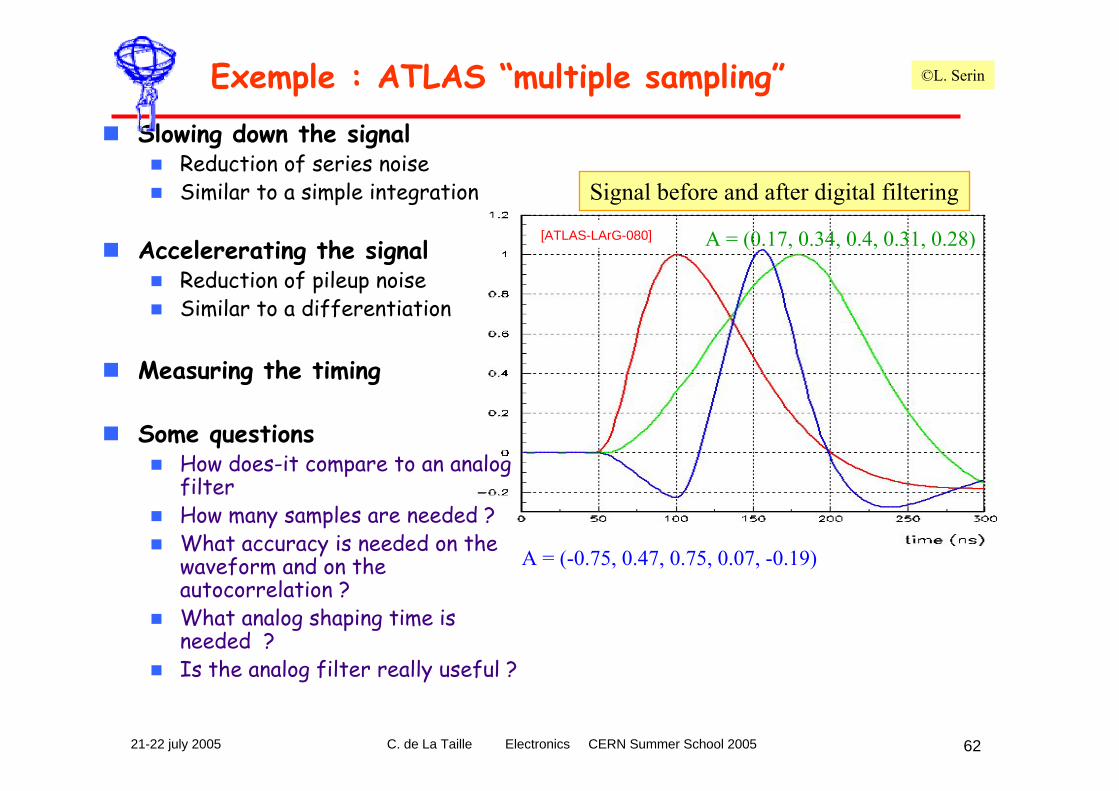
Exemple : ATLAS “multiple sampling”Slowing down the signal
Reduction of series noiseSimilar to a simple integration
Accelererating the signalReduction of pileup noiseSimilar to a differentiation
Measuring the timing
Some questionsHow does-it compare to an analogfilterHow many samples are needed ?What accuracy is needed on thewaveform and on theautocorrelation ?What analog shaping time isneeded ?Is the analog filter really useful ?
A = (0.17, 0.34, 0.4, 0.31, 0.28)
A = (-0.75, 0.47, 0.75, 0.07, -0.19)
Signal before and after digital filtering
[ATLAS-LArG-080]
©L. Serin
21-22 july 2005 C. de La Taille Electronics CERN Summer School 2005 63
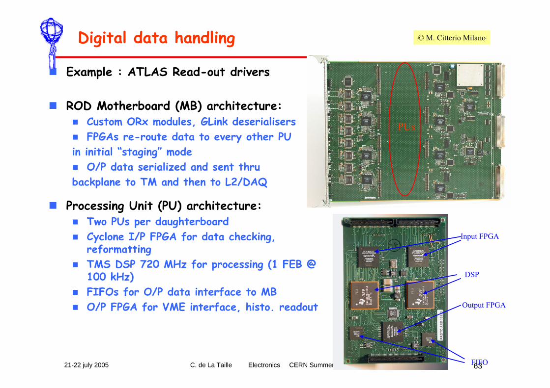
Digital data handling
Example : ATLAS Read-out drivers
ROD Motherboard (MB) architecture:Custom ORx modules, GLink deserialisersFPGAs re-route data to every other PU
in initial “staging” modeO/P data serialized and sent thru
backplane to TM and then to L2/DAQ
Processing Unit (PU) architecture:Two PUs per daughterboardCyclone I/P FPGA for data checking, reformattingTMS DSP 720 MHz for processing (1 FEB @ 100 kHz)FIFOs for O/P data interface to MBO/P FPGA for VME interface, histo. readout
Input FPGA
DSP
Output FPGA
FIFO
PUs
© M. Citterio Milano
21-22 july 2005 C. de La Taille Electronics CERN Summer School 2005 64
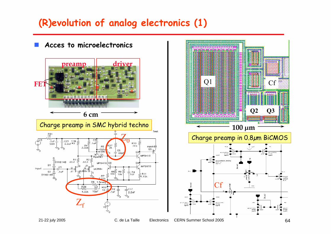
(R)evolution of analog electronics (1)
Acces to microelectronics
6 cm
FET
driverpreamp
100 µm
Zf
Z0
Q2
CfQ1
Q3
Cf
Charge preamp in 0.8µm BiCMOS
Charge preamp in SMC hybrid techno
21-22 july 2005 C. de La Taille Electronics CERN Summer School 2005 65
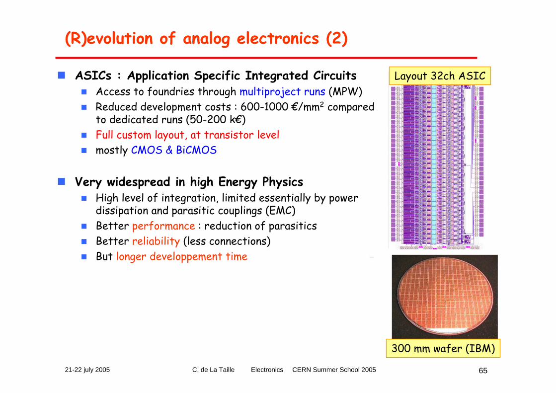
(R)evolution of analog electronics (2)
ASICs : Application Specific Integrated CircuitsAccess to foundries through multiproject runs (MPW) Reduced development costs : 600-1000 €/mm2 comparedto dedicated runs (50-200 k€)Full custom layout, at transistor levelmostly CMOS & BiCMOS
Very widespread in high Energy PhysicsHigh level of integration, limited essentially by powerdissipation and parasitic couplings (EMC)Better performance : reduction of parasiticsBetter reliability (less connections)But longer developpement time
Layout 32ch ASIC
300 mm wafer (IBM)
21-22 july 2005 C. de La Taille Electronics CERN Summer School 2005 66
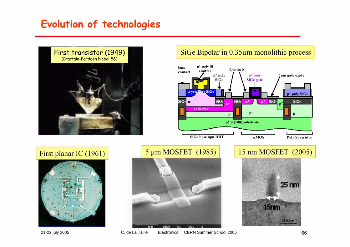
Evolution of technologies
First transistor (1949)(Brattain-Bardeen Nobel 56)
5 µm MOSFET (1985) 15 nm MOSFET (2005)First planar IC (1961)
SiGe Bipolar in 0.35µm monolithic process
21-22 july 2005 C. de La Taille Electronics CERN Summer School 2005 67
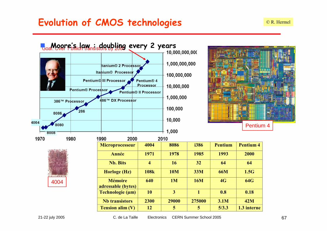
Evolution of CMOS technologies
Moore’s law : doubling every 2 years
Microprocesseur 4004 8086 i386 Pentium Pentium 4
Année 1971 1978 1985 1993 2000
Nb. Bits 4 16 32 64 64
Horloge (Hz) 108k 10M 33M 66M 1.5G
Mémoire adressable (bytes)
640 1M 16M 4G 64G
Technologie (µm) 10 3 1 0.8 0.18
Nb transistors 2300 29000 275000 3.1M 42M Tension alim (V) 12 5 5 5/3.3 1.3 interne
Pentium 4
4004
© R. Hermel
21-22 july 2005 C. de La Taille Electronics CERN Summer School 2005 68
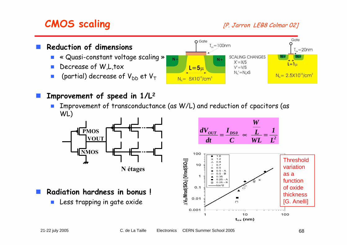
CMOS scaling [P. Jarron LEB8 Colmar 02]
Reduction of dimensions « Quasi-constant voltage scaling »Decrease of W,L,tox(partial) decrease of VDD et VT
Improvement of speed in 1/L2
Improvement of transconductance (as W/L) and reduction of cpacitors (as WL)
Radiation hardness in bonus !Less trapping in gate oxide
PMOS
NMOS
VOUT
N étages
20DSOUT
L1
WLL
W
CI
dtdV =∝=
Thresholdvariationas a function of oxide thickness[G. Anelli]
21-22 july 2005 C. de La Taille Electronics CERN Summer School 2005 69
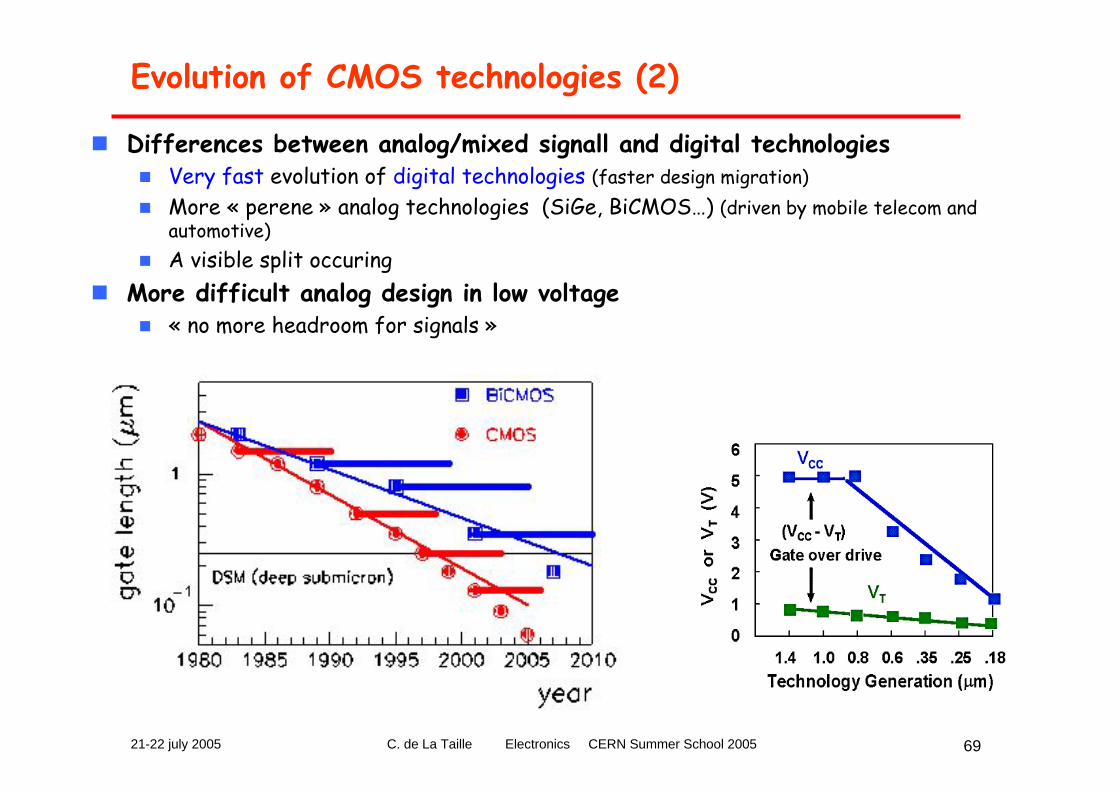
Evolution of CMOS technologies (2)
Differences between analog/mixed signall and digital technologies Very fast evolution of digital technologies (faster design migration)More « perene » analog technologies (SiGe, BiCMOS…) (driven by mobile telecom andautomotive)A visible split occuring
More difficult analog design in low voltage« no more headroom for signals »
21-22 july 2005 C. de La Taille Electronics CERN Summer School 2005 70
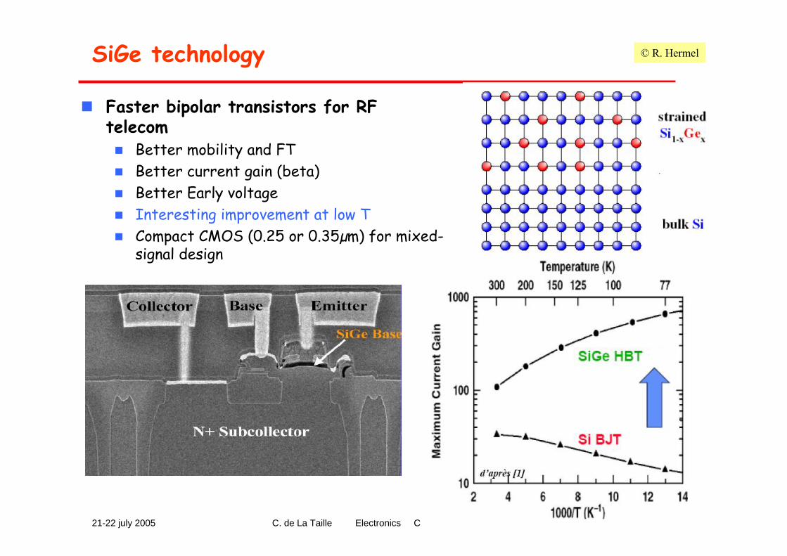
SiGe technology
Faster bipolar transistors for RF telecom
Better mobility and FTBetter current gain (beta)Better Early voltageInteresting improvement at low TCompact CMOS (0.25 or 0.35µm) for mixed-signal design
© R. Hermel
21-22 july 2005 C. de La Taille Electronics CERN Summer School 2005 71
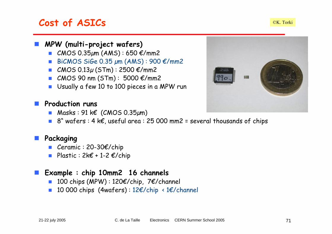
Cost of ASICs
MPW (multi-project wafers)CMOS 0.35µm (AMS) : 650 €/mm2BiCMOS SiGe 0.35 µm (AMS) : 900 €/mm2CMOS 0.13µ (STm) : 2500 €/mm2CMOS 90 nm (STm) : 5000 €/mm2Usually a few 10 to 100 pieces in a MPW run
Production runsMasks : 91 k€ (CMOS 0.35µm)8“ wafers : 4 k€, useful area : 25 000 mm2 = several thousands of chips
PackagingCeramic : 20-30€/chipPlastic : 2k€ + 1-2 €/chip
Example : chip 10mm2 16 channels100 chips (MPW) : 120€/chip, 7€/channel10 000 chips (4wafers) : 12€/chip < 1€/channel
©K. Torki
21-22 july 2005 C. de La Taille Electronics CERN Summer School 2005 72
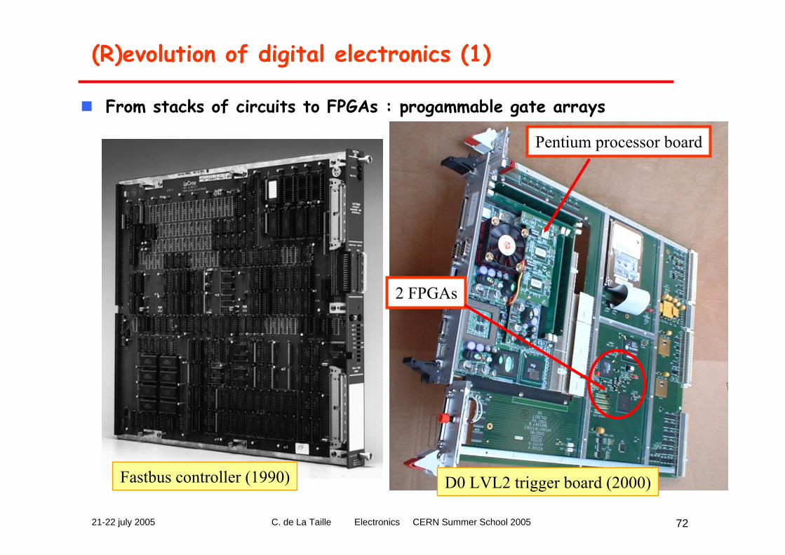
(R)evolution of digital electronics (1)
From stacks of circuits to FPGAs : progammable gate arrays
2 FPGAs
Pentium processor board
Fastbus controller (1990) D0 LVL2 trigger board (2000)
21-22 july 2005 C. de La Taille Electronics CERN Summer School 2005 73
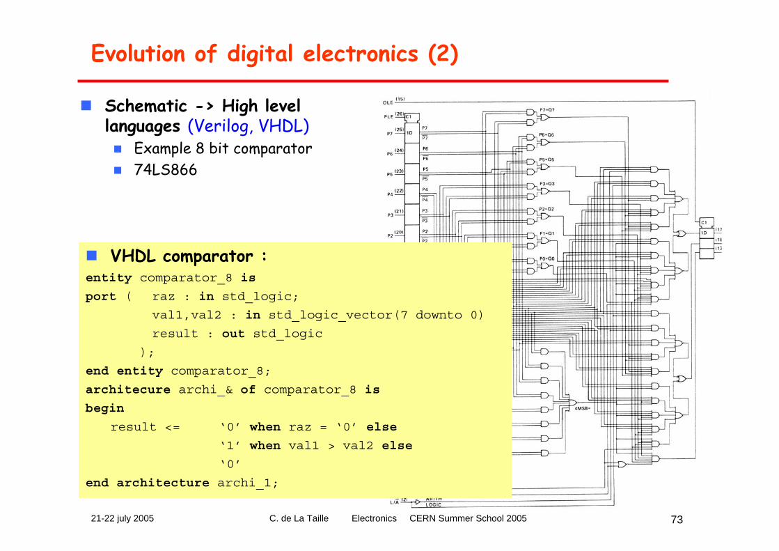
Evolution of digital electronics (2)
Schematic -> High levellanguages (Verilog, VHDL)
Example 8 bit comparator74LS866
VHDL comparator :entity comparator_8 is
port ( raz : in std_logic;
val1,val2 : in std_logic_vector(7 downto 0)
result : out std_logic
);
end entity comparator_8;
architecure archi_& of comparator_8 is
begin
result <= ‘0’ when raz = ‘0’ else
‘1’ when val1 > val2 else
‘0’
end architecture archi_1;
21-22 july 2005 C. de La Taille Electronics CERN Summer School 2005 74
(R)evolution of digital electronics (3)
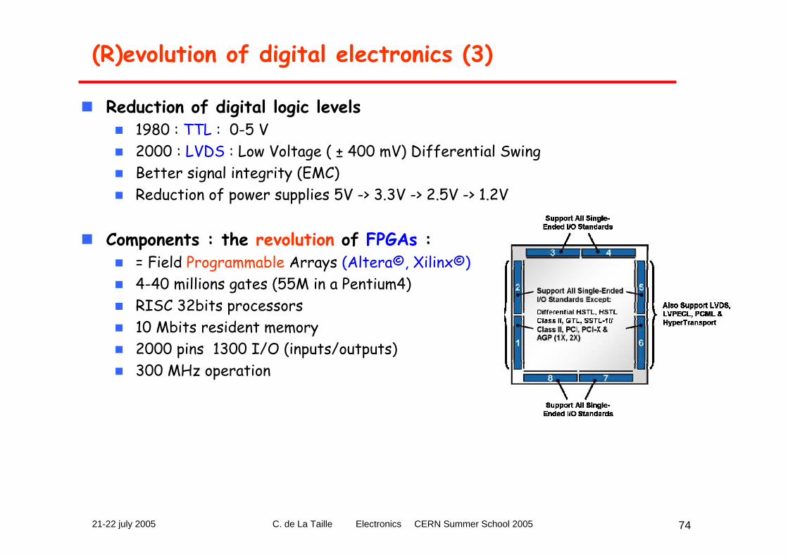
Reduction of digital logic levels1980 : TTL : 0-5 V2000 : LVDS : Low Voltage ( ± 400 mV) Differential SwingBetter signal integrity (EMC)Reduction of power supplies 5V -> 3.3V -> 2.5V -> 1.2V
Components : the revolution of FPGAs : = Field Programmable Arrays (Altera©, Xilinx©)4-40 millions gates (55M in a Pentium4)RISC 32bits processors10 Mbits resident memory2000 pins 1300 I/O (inputs/outputs)300 MHz operation
21-22 july 2005 C. de La Taille Electronics CERN Summer School 2005 75
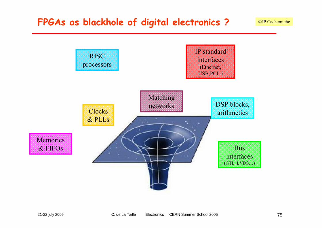
FPGAs as blackhole of digital electronics ?
Memories& FIFOs
Clocks& PLLs
Bus interfaces
(GTL, LVDS…)
DSP blocks, arithmetics
RISC processors
IP standard interfaces
(Ethernet, USB,PCI..)
Matchingnetworks
©JP Cachemiche
21-22 july 2005 C. de La Taille Electronics CERN Summer School 2005 76
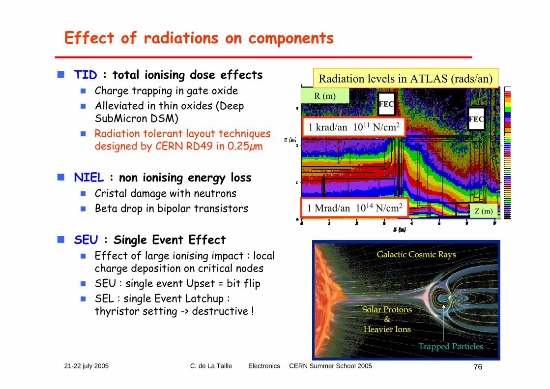
Effect of radiations on components
TID : total ionising dose effectsCharge trapping in gate oxideAlleviated in thin oxides (DeepSubMicron DSM)Radiation tolerant layout techniques designed by CERN RD49 in 0.25µm
NIEL : non ionising energy lossCristal damage with neutronsBeta drop in bipolar transistors
SEU : Single Event EffectEffect of large ionising impact : local charge deposition on critical nodesSEU : single event Upset = bit flipSEL : single Event Latchup : thyristor setting -> destructive !
FEC
FEC
Z (m)
R (m)
Radiation levels in ATLAS (rads/an)
1 Mrad/an 1014 N/cm2
1 krad/an 1011 N/cm2
21-22 july 2005 C. de La Taille Electronics CERN Summer School 2005 77
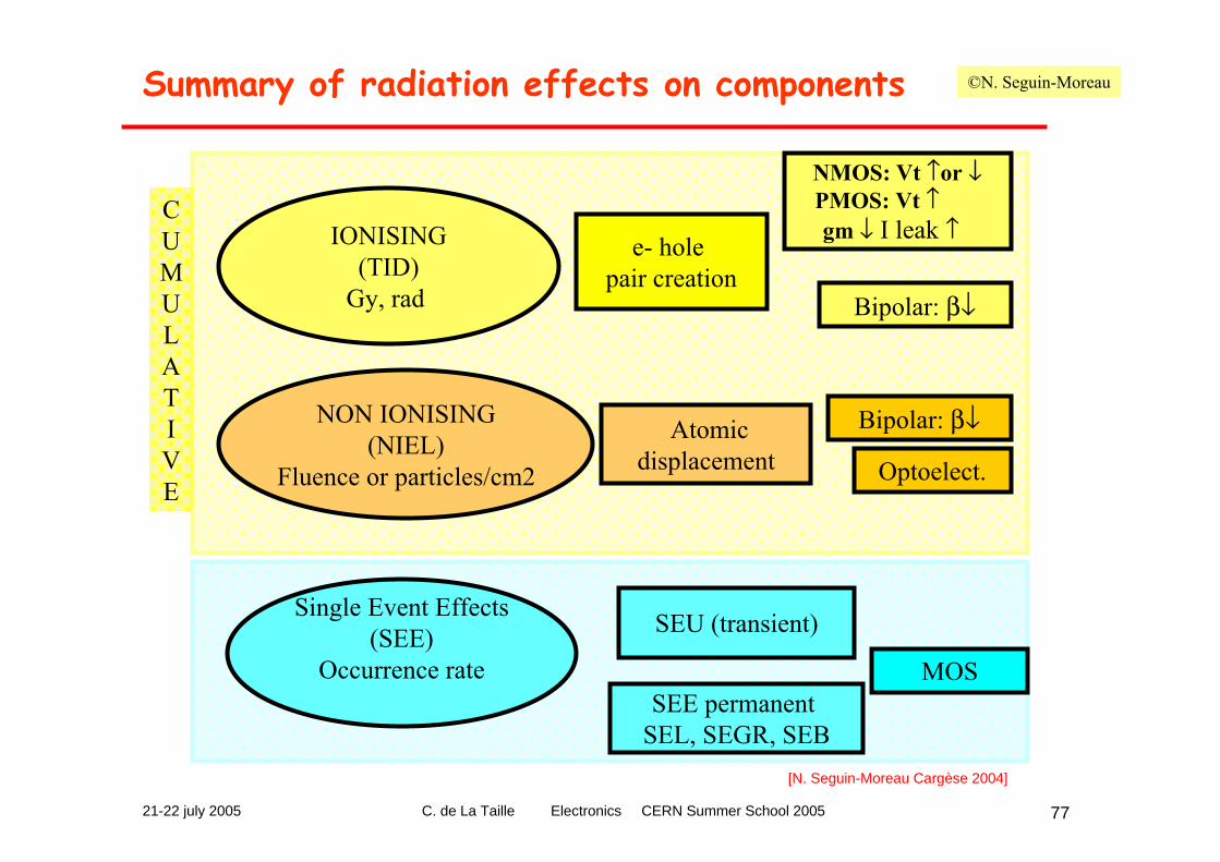
Summary of radiation effects on components
IONISING(TID)
Gy, rad
NMOS: Vt ↑or ↓PMOS: Vt ↑gm ↓ I leak ↑
Bipolar: β↓
NON IONISING(NIEL)
Fluence or particles/cm2
Atomicdisplacement
Single Event Effects(SEE)
Occurrence rateSEE permanent
SEL, SEGR, SEB
SEU (transient)
CUMULATIVE
e- holepair creation
Bipolar: β↓
Optoelect.
MOS
[N. Seguin-Moreau Cargèse 2004]
©N. Seguin-Moreau
21-22 july 2005 C. de La Taille Electronics CERN Summer School 2005 78
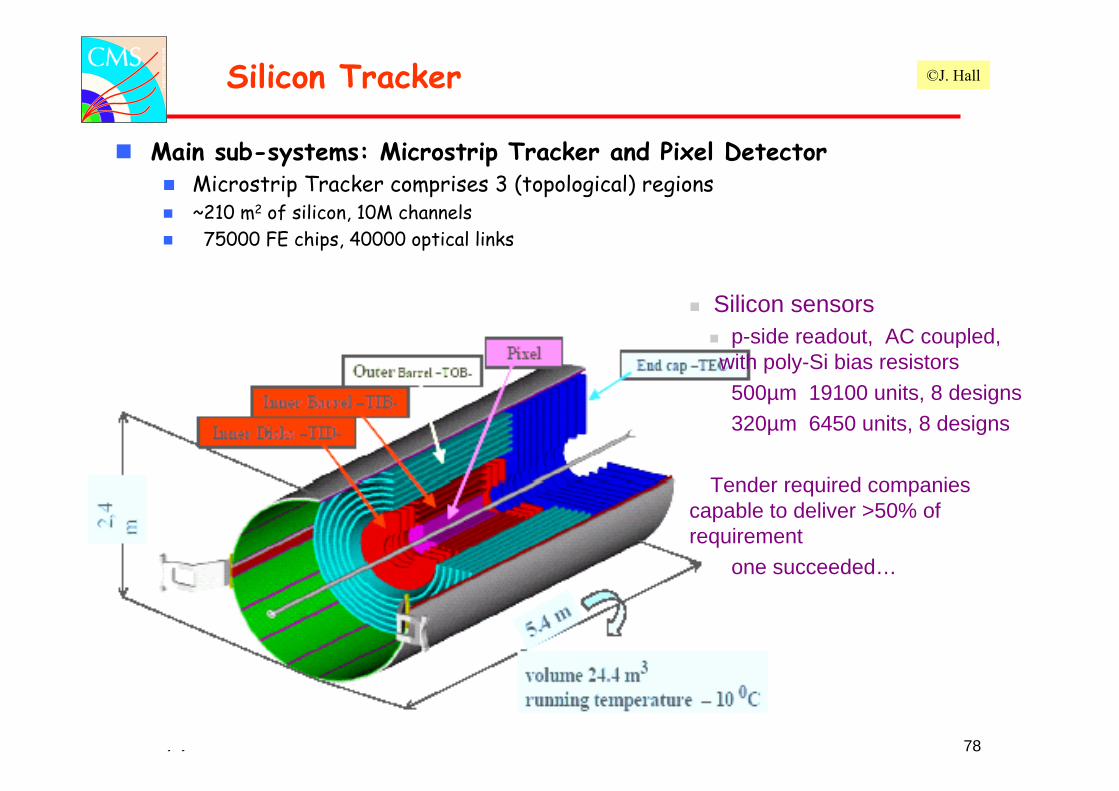
Silicon Tracker
Main sub-systems: Microstrip Tracker and Pixel DetectorMicrostrip Tracker comprises 3 (topological) regions~210 m2 of silicon, 10M channels 75000 FE chips, 40000 optical links
Silicon sensors p-side readout, AC coupled,
with poly-Si bias resistors500µm 19100 units, 8 designs320µm 6450 units, 8 designs
Tender required companies capable to deliver >50% of requirement
one succeeded…
©J. Hall
21-22 july 2005 C. de La Taille Electronics CERN Summer School 2005 79
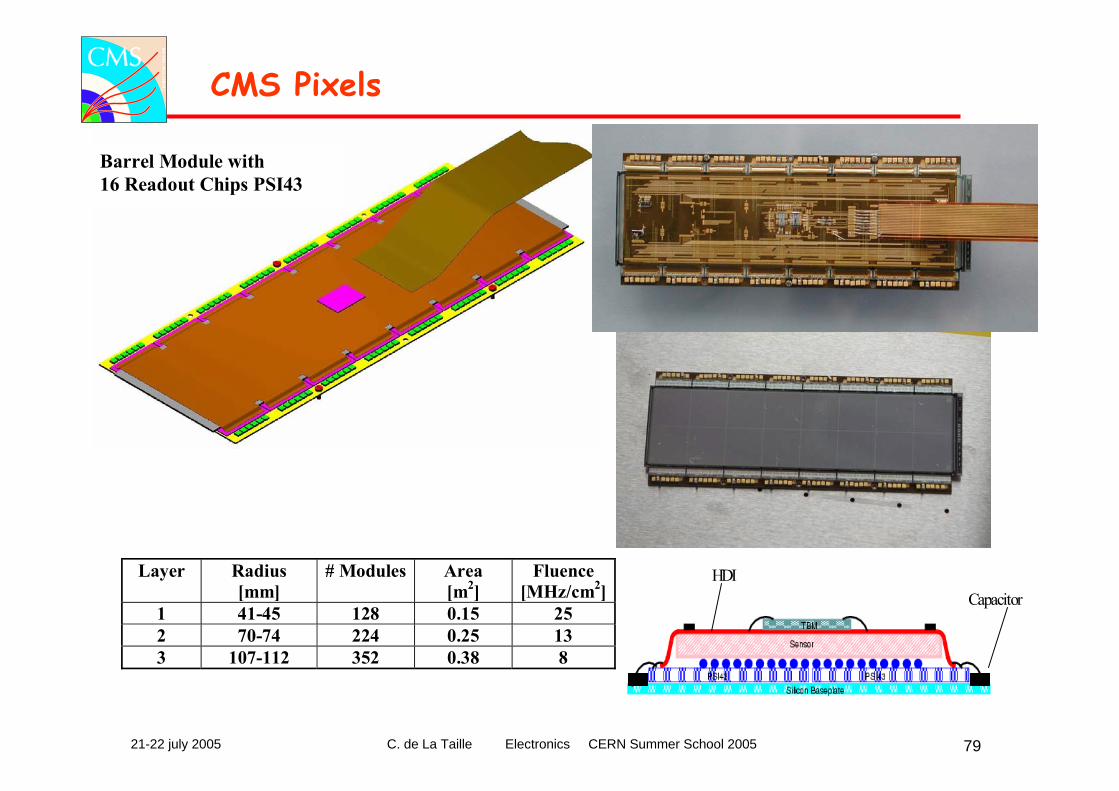
CMS Pixels
Layer Radius[mm]
# Modules Area[m2]
Fluence[MHz/cm2]
1 41-45 128 0.15 252 70-74 224 0.25 133 107-112 352 0.38 8
Barrel Module with16 Readout Chips PSI43
HDICapacitor
21-22 july 2005 C. de La Taille Electronics CERN Summer School 2005 80
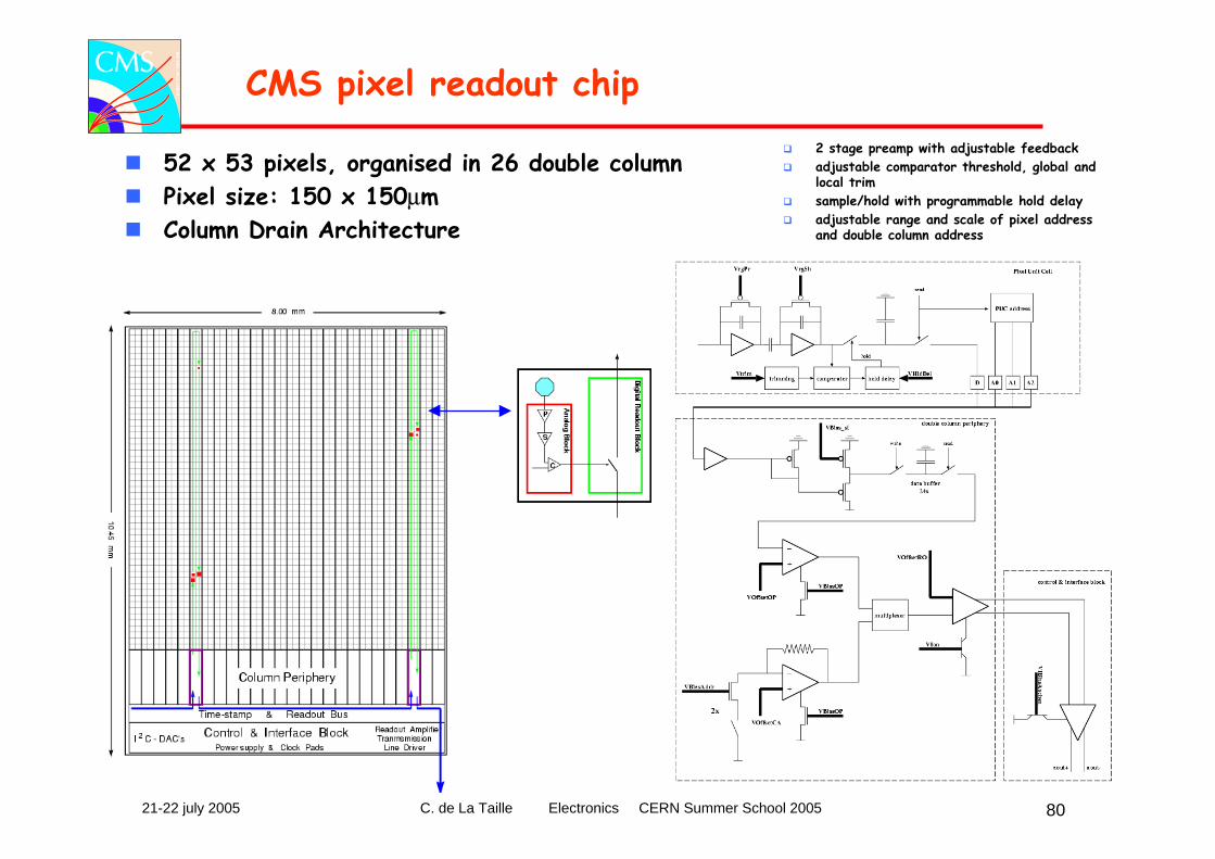
CMS pixel readout chip
52 x 53 pixels, organised in 26 double columnPixel size: 150 x 150μmColumn Drain Architecture
2 stage preamp with adjustable feedbackadjustable comparator threshold, global and local trimsample/hold with programmable hold delayadjustable range and scale of pixel addressand double column address
21-22 july 2005 C. de La Taille Electronics CERN Summer School 2005 81
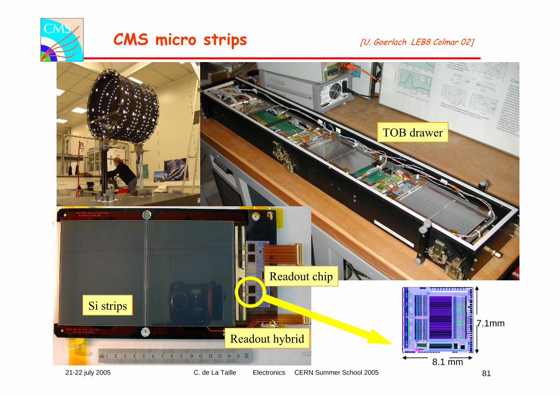
CMS micro strips [U. Goerlach LEB8 Colmar 02]
TOB drawer
Si strips
Readout hybrid
Readout chip
7.1mm
8.1 mm
21-22 july 2005 C. de La Taille Electronics CERN Summer School 2005 82
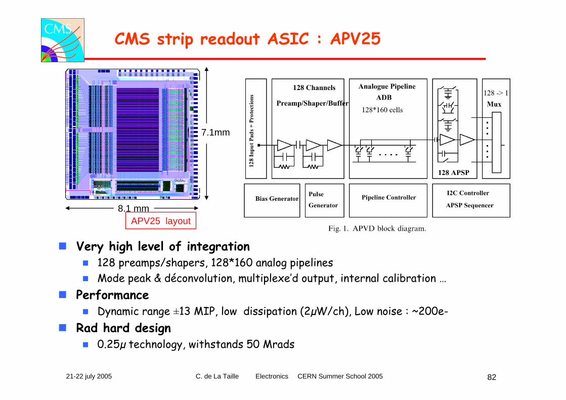
CMS strip readout ASIC : APV25
Very high level of integration128 preamps/shapers, 128*160 analog pipelinesMode peak & déconvolution, multiplexe’d output, internal calibration …
PerformanceDynamic range ±13 MIP, low dissipation (2µW/ch), Low noise : ~200e-
Rad hard design 0.25µ technology, withstands 50 Mrads
APV25 layout
7.1mm
8.1 mm
21-22 july 2005 C. de La Taille Electronics CERN Summer School 2005 83
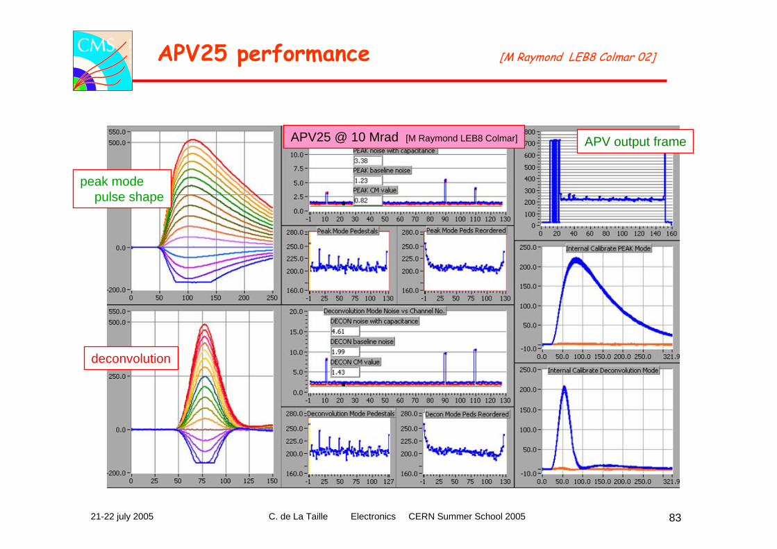
APV25 performance [M Raymond LEB8 Colmar 02]
deconvolution
peak modepulse shape
APV output frameAPV25 @ 10 Mrad [M Raymond LEB8 Colmar]
21-22 july 2005 C. de La Taille Electronics CERN Summer School 2005 84
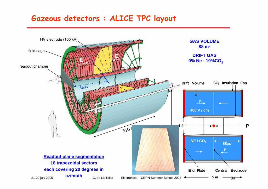
Gazeous detectors : ALICE TPC layout
GAS VOLUME88 m3
DRIFT GAS90% Ne - 10%CO2
Readout plane segmentation18 trapezoidal sectors
each covering 20 degrees in azimuth
E E
510 cm
E E
88us
Pb P
E
E
CO2 Insulation GapDrift Volume
End Plate Central Electrode5 m
5.6 m
1.6
400 V / cm
NE / CO2 88μs
21-22 july 2005 C. de La Taille Electronics CERN Summer School 2005 85
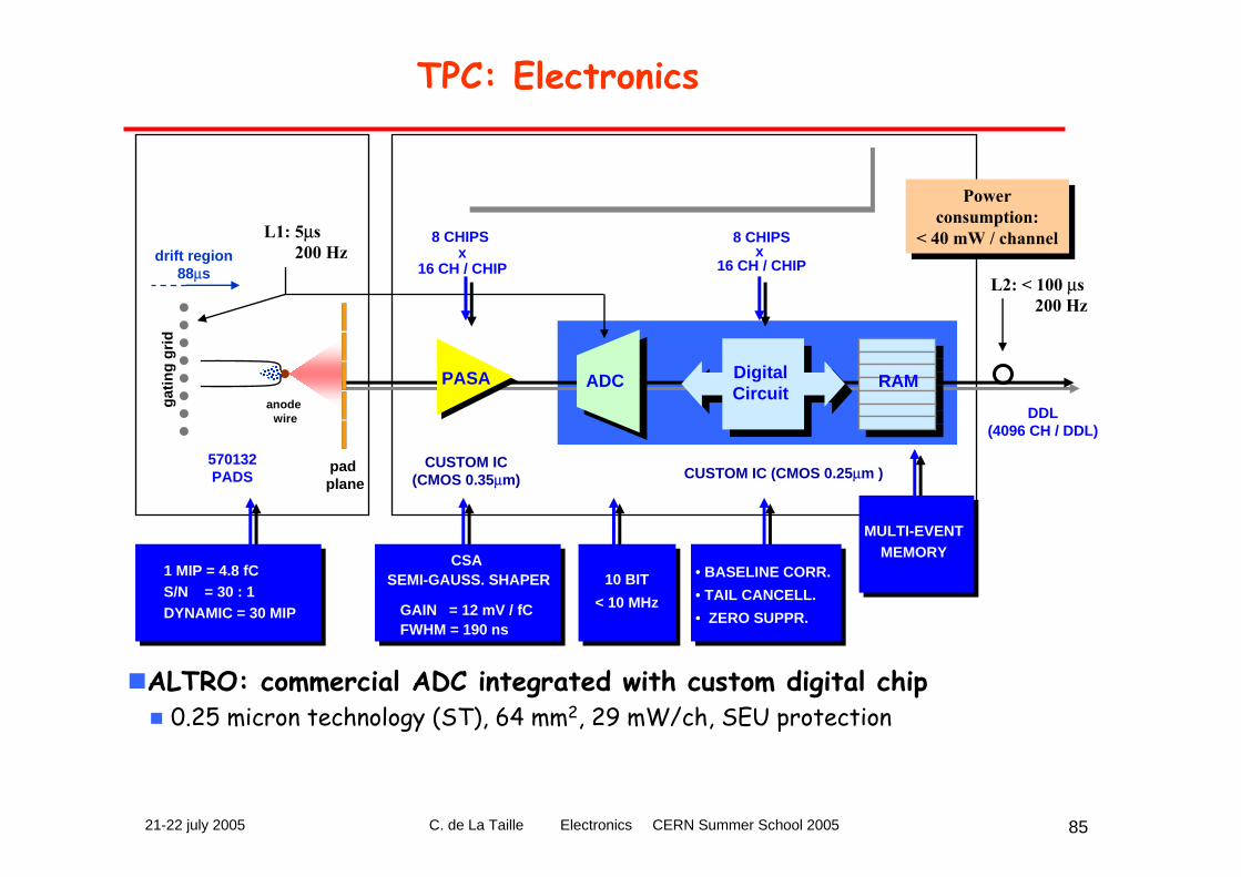
TPC: Electronics
ALTRO: commercial ADC integrated with custom digital chip0.25 micron technology (ST), 64 mm2, 29 mW/ch, SEU protection
anode wire
pad plane
drift region88μs
L1: 5μs200 Hz
PASA ADC DigitalCircuit
RAM
8 CHIPS x
16 CH / CHIP
8 CHIPSx
16 CH / CHIP
CUSTOM IC(CMOS 0.35μm) CUSTOM IC (CMOS 0.25μm )
DETECTOR FEC (Front End Card) - 128 CHANNELS(CLOSE TO THE READOUT PLANE)
FEC (Front End Card) - 128 CHANNELS(CLOSE TO THE READOUT PLANE)
570132PADS
1 MIP = 4.8 fCS/N = 30 : 1DYNAMIC = 30 MIP
CSA SEMI-GAUSS. SHAPER
GAIN = 12 mV / fCFWHM = 190 ns
10 BIT< 10 MHz
• BASELINE CORR.• TAIL CANCELL.• ZERO SUPPR.
MULTI-EVENTMEMORY
L2: < 100 μs200 Hz
DDL(4096 CH / DDL)
Powerconsumption:
< 40 mW / channel
Powerconsumption:
< 40 mW / channel
gatin
g gr
id
21-22 july 2005 C. de La Taille Electronics CERN Summer School 2005 86
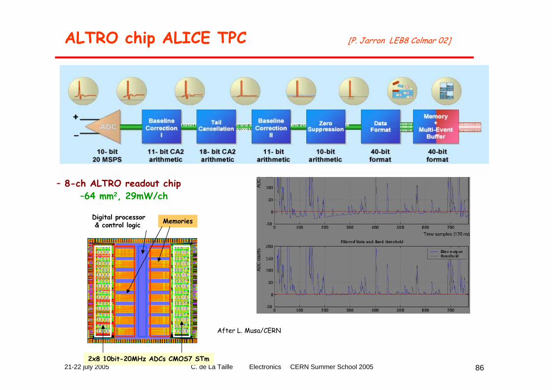
ALTRO chip ALICE TPC [P. Jarron LEB8 Colmar 02]
– 8-ch ALTRO readout chip–64 mm2, 29mW/ch
2x8 10bit-20MHz ADCs CMOS7 STm
MemoriesDigital processor& control logic
After L. Musa/CERN
21-22 july 2005 C. de La Taille Electronics CERN Summer School 2005 87
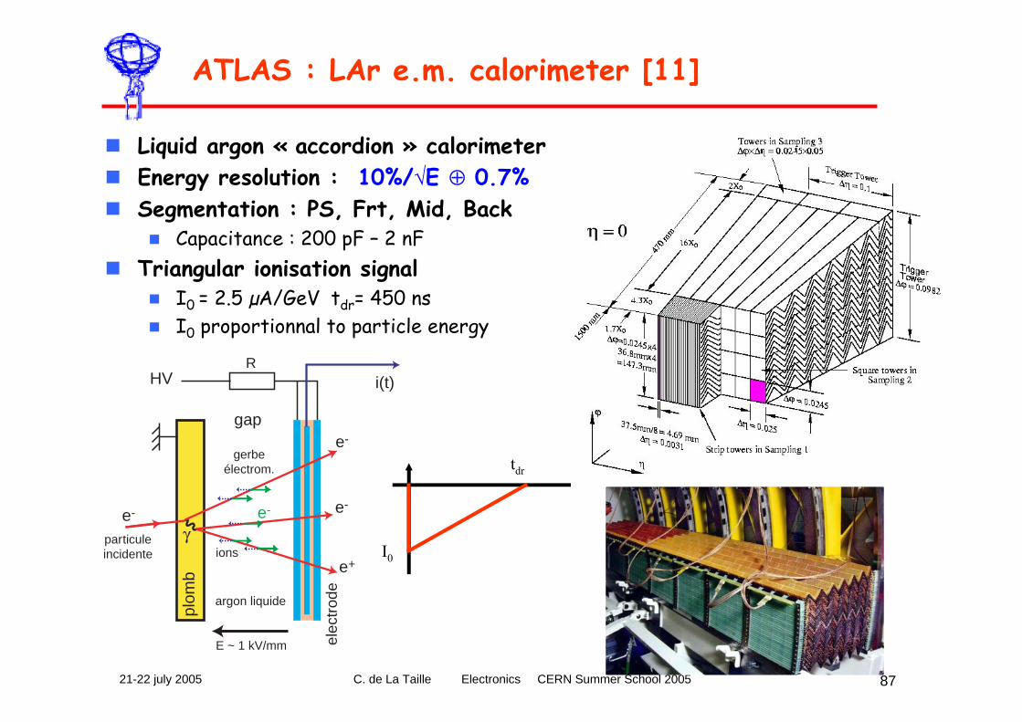
ATLAS : LAr e.m. calorimeter [11]
Liquid argon « accordion » calorimeterEnergy resolution : 10%/√E ⊕ 0.7%Segmentation : PS, Frt, Mid, Back
Capacitance : 200 pF – 2 nFTriangular ionisation signal
I0 = 2.5 µA/GeV tdr= 450 nsI0 proportionnal to particle energy
tdr
I0
RHV i(t)
gap
gerbeélectrom.
plom
b
E ~ 1 kV/mm elec
trod
e
e- e-
e+
γe-
ions
argon liquide
particuleincidente
e-
21-22 july 2005 C. de La Taille Electronics CERN Summer School 2005 88
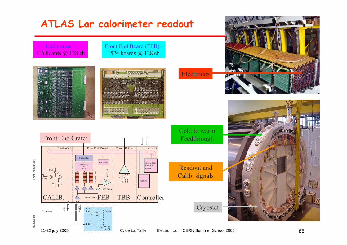
Laye
r Sum
Shapers
Calibration
DAC
LcRc
Clock
I
Preamplifiers
Σ
Buffering & ADC
Optical Link
T=90K
Cd
Front End Board Tower Builder Control
40MHz CLK
LV1 Acc.
Control
Reset
~180
k
~15k
Σ
Cryostat
On Detector
Fron
t End
Cra
te (6
0)M
othe
rboa
rd
Controller
SCA
(144
Cel
ls)
Calibration :116 boards @ 128 ch
Front End Board (FEB) :1524 boards @ 128 ch
Electrodes
Cryostat
Cold to warm Feedthrough
Readout and Calib. signals
Front End Crate:
CALIB. FEB TBB Controller
ATLAS Lar calorimeter readout
21-22 july 2005 C. de La Taille Electronics CERN Summer School 2005 89
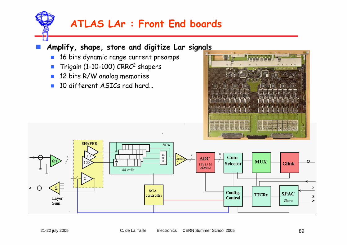
ATLAS LAr : Front End boards
Amplify, shape, store and digitize Lar signals16 bits dynamic range current preampsTrigain (1-10-100) CRRC2 shapers12 bits R/W analog memories10 different ASICs rad hard…
21-22 july 2005 C. de La Taille Electronics CERN Summer School 2005 90
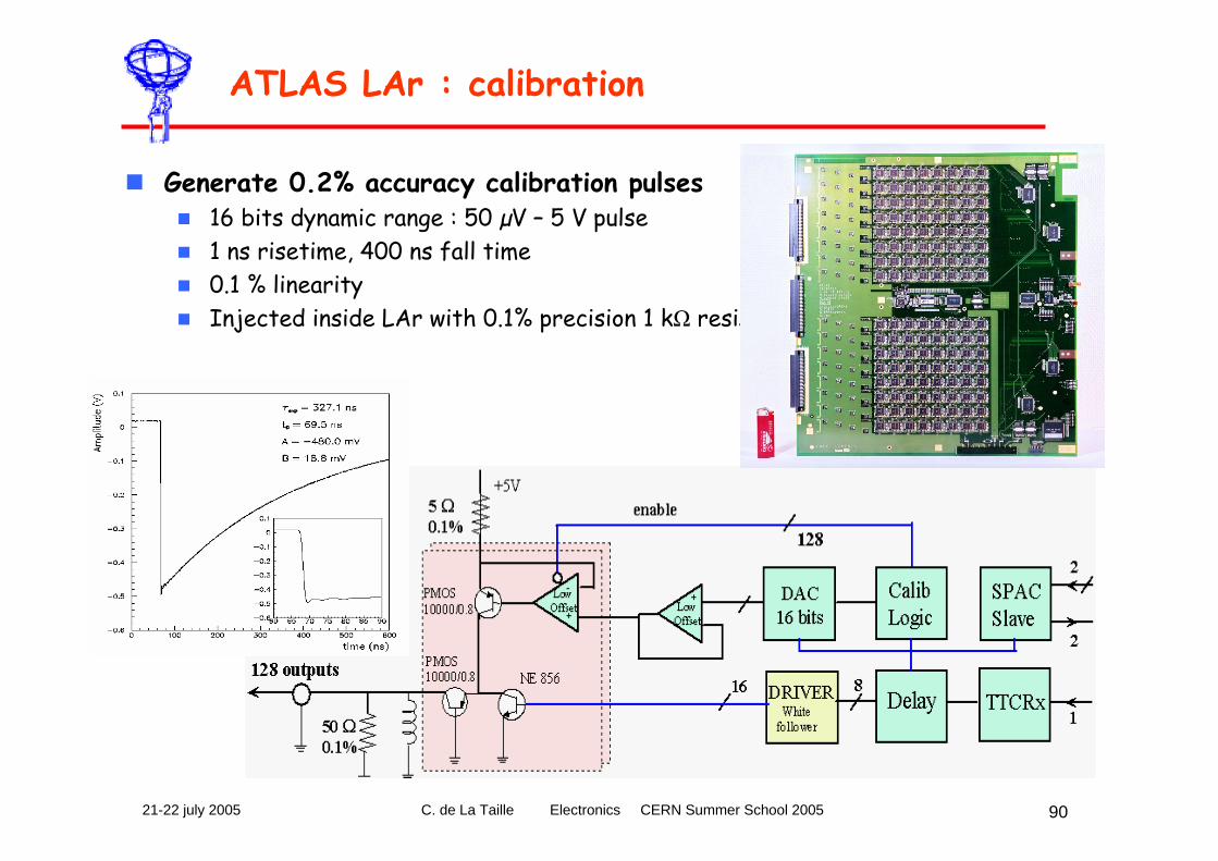
ATLAS LAr : calibration
Generate 0.2% accuracy calibration pulses16 bits dynamic range : 50 µV – 5 V pulse1 ns risetime, 400 ns fall time0.1 % linearityInjected inside LAr with 0.1% precision 1 kΩ resistors
21-22 july 2005 C. de La Taille Electronics CERN Summer School 2005 91
Future : ILC challenges for electronics
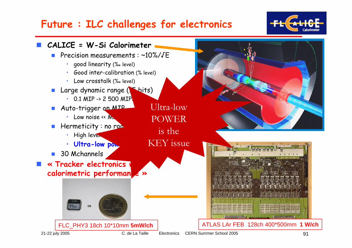
CALICE = W-Si CalorimeterPrecision measurements : ~10%/√E
• good linearity (‰ level)• Good inter-calibration (% level)• Low crosstalk (‰ level)
Large dynamic range (15 bits)• 0.1 MIP -> 2 500 MIPS
Auto-trigger on MIP • Low noise << MIP = 40, 000 e-
Hermeticity : no room for electronics !• High level of integration : « SoC »• Ultra-low power : ( << mW/ch)
30 Mchannels« Tracker electronics withcalorimetric performance »
ATLAS LAr FEB 128ch 400*500mm 1 W/chFLC_PHY3 18ch 10*10mm 5mW/ch
Ultra-lowPOWER
is theKEY issue
21-22 july 2005 C. de La Taille Electronics CERN Summer School 2005 92
Future : calorimetry at ILC (201?)
1.5m
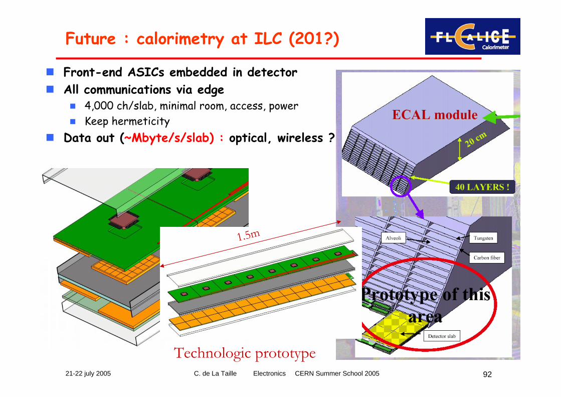
Technologic prototype
Front-end ASICs embedded in detectorAll communications via edge
4,000 ch/slab, minimal room, access, powerKeep hermeticity
Data out (~Mbyte/s/slab) : optical, wireless ?
21-22 july 2005 C. de La Taille Electronics CERN Summer School 2005 93
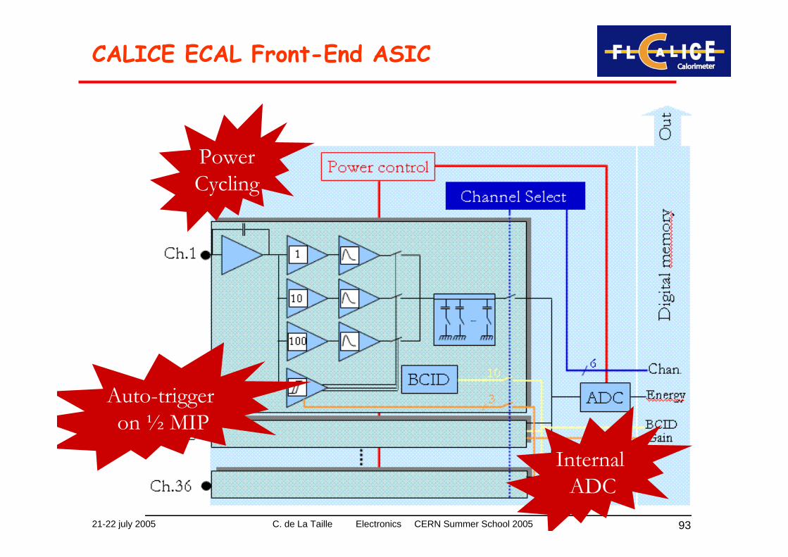
CALICE ECAL Front-End ASIC
PowerCycling
Auto-triggeron ½ MIP
InternalADC
21-22 july 2005 C. de La Taille Electronics CERN Summer School 2005 94
Electromagnetic compatibility (EMC-EMI)
Coexistence analog-digitalCapacitive, inductive and common-impedance couplingsA full lecture !A good summary : there is no such thing as « ground », pay attention to currentreturn
21-22 july 2005 C. de La Taille Electronics CERN Summer School 2005 95
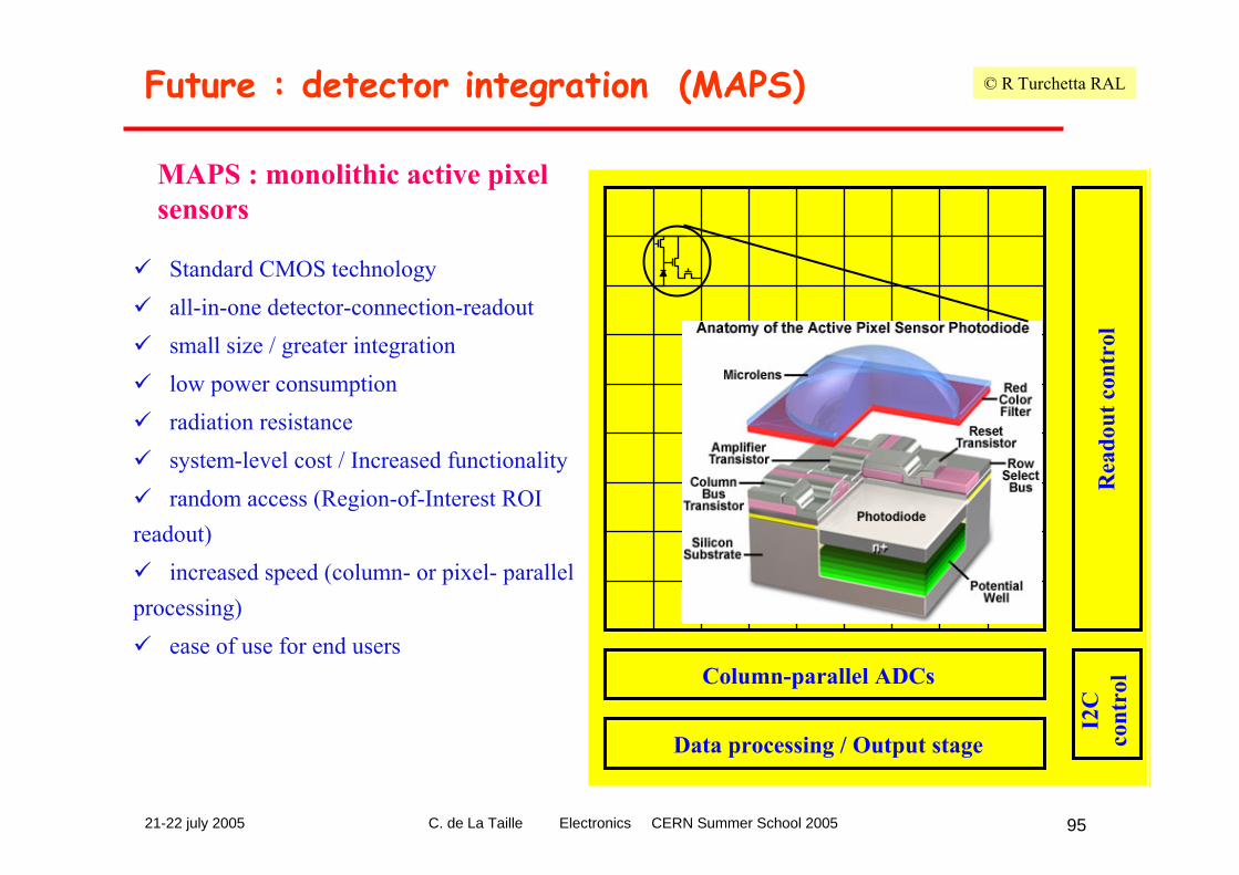
MAPS : monolithic active pixel sensors
Standard CMOS technologyall-in-one detector-connection-readoutsmall size / greater integrationlow power consumptionradiation resistancesystem-level cost / Increased functionalityrandom access (Region-of-Interest ROI
readout)increased speed (column- or pixel- parallel
processing)ease of use for end users
Column-parallel ADCs
Data processing / Output stage
Rea
dout
con
trol
I2C
co
ntro
l
Future : detector integration (MAPS) © R Turchetta RAL
21-22 july 2005 C. de La Taille Electronics CERN Summer School 2005 96
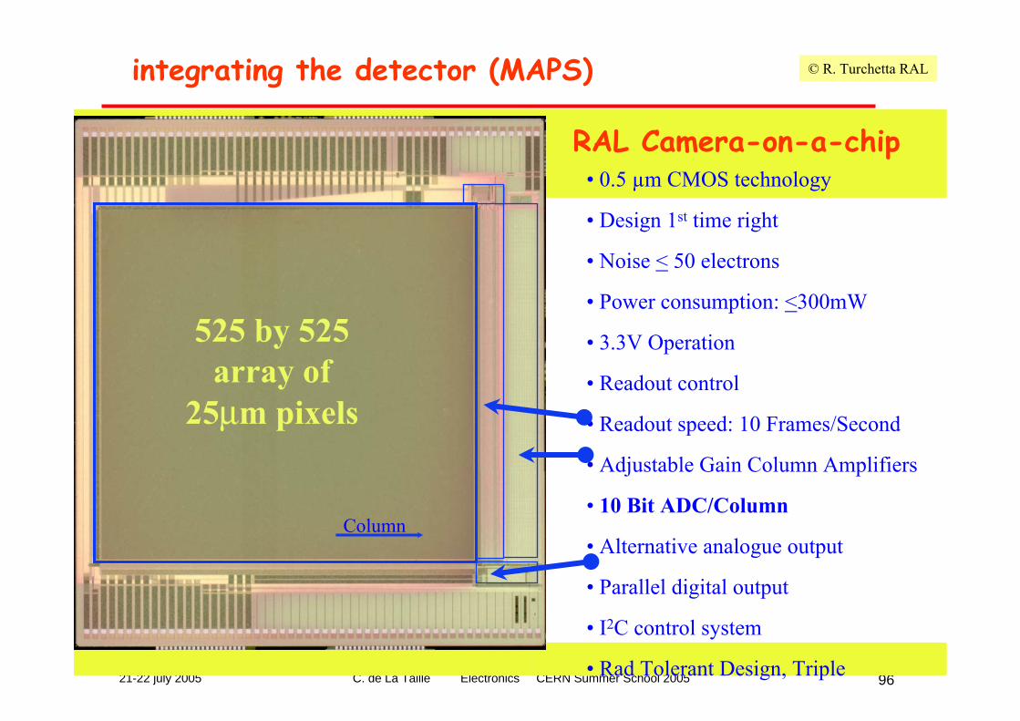
integrating the detector (MAPS) © R. Turchetta RAL
• 0.5 µm CMOS technology
• Design 1st time right
• Noise < 50 electrons
• Power consumption: <300mW
• 3.3V Operation
• Readout control
• Readout speed: 10 Frames/Second
• Adjustable Gain Column Amplifiers
• 10 Bit ADC/Column
• Alternative analogue output
• Parallel digital output
• I2C control system
• Rad Tolerant Design, Triple d d i
Column
525 by 525 array of
25μm pixels
RAL Camera-on-a-chip
21-22 july 2005 C. de La Taille Electronics CERN Summer School 2005 97
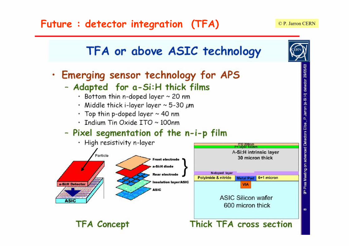
Future : detector integration (TFA) © P. Jarron CERN
21-22 july 2005 C. de La Taille Electronics CERN Summer School 2005 98
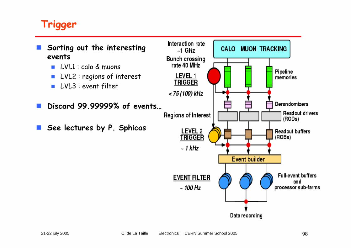
Trigger
Sorting out the interestingevents
LVL1 : calo & muonsLVL2 : regions of interestLVL3 : event filter
Discard 99.99999% of events…
See lectures by P. Sphicas
21-22 july 2005 C. de La Taille Electronics CERN Summer School 2005 99
Conclusion
In High Energy Physics, electronics isEverywhere, from detector to control roomsEssential for performanceCustomized inside ASICsUsing (and pushing) state of the art technology
I hope the 3 lectures convinced you thatIt is easy to understandIt is sometimes an Art, but always accessibleIt is interesting and even fun…