Embed Size (px)
Citation preview
Intro to UARTs
April 2010
Why use a UART?
• UARTs are everywhere!• Simple way to send data from one system to
another system• Add additional functionality to an application
2
Why use a UART from Exar?
• Largest and broadest UART portfolio• Highest performance UARTs• UARTs with the most enhanced features• Excellent technical support• Exar also has serial transceivers!
3
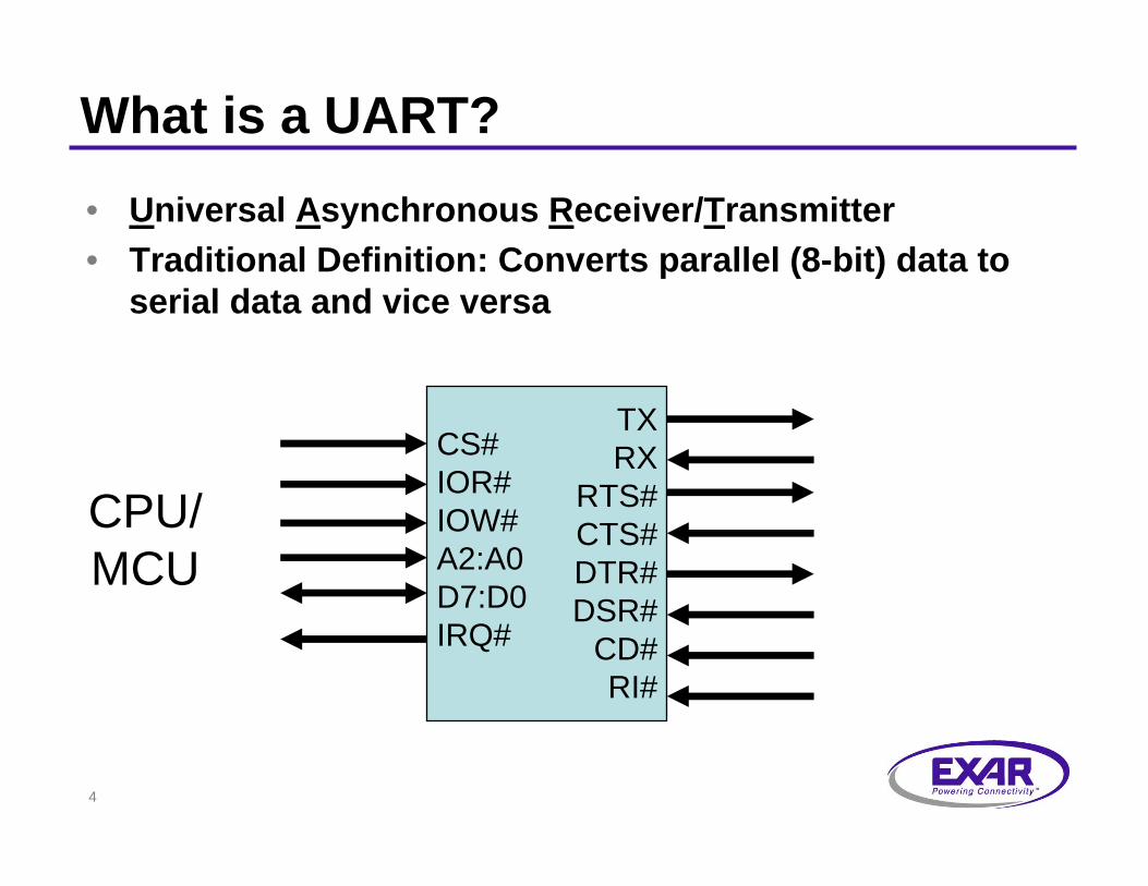
4
What is a UART?• Universal Asynchronous Receiver/Transmitter• Traditional Definition: Converts parallel (8-bit) data to
serial data and vice versa
TXRX
RTS#CTS#DTR#DSR#
CD#RI#
CS#IOR#IOW#A2:A0D7:D0IRQ#
CPU/MCU
5
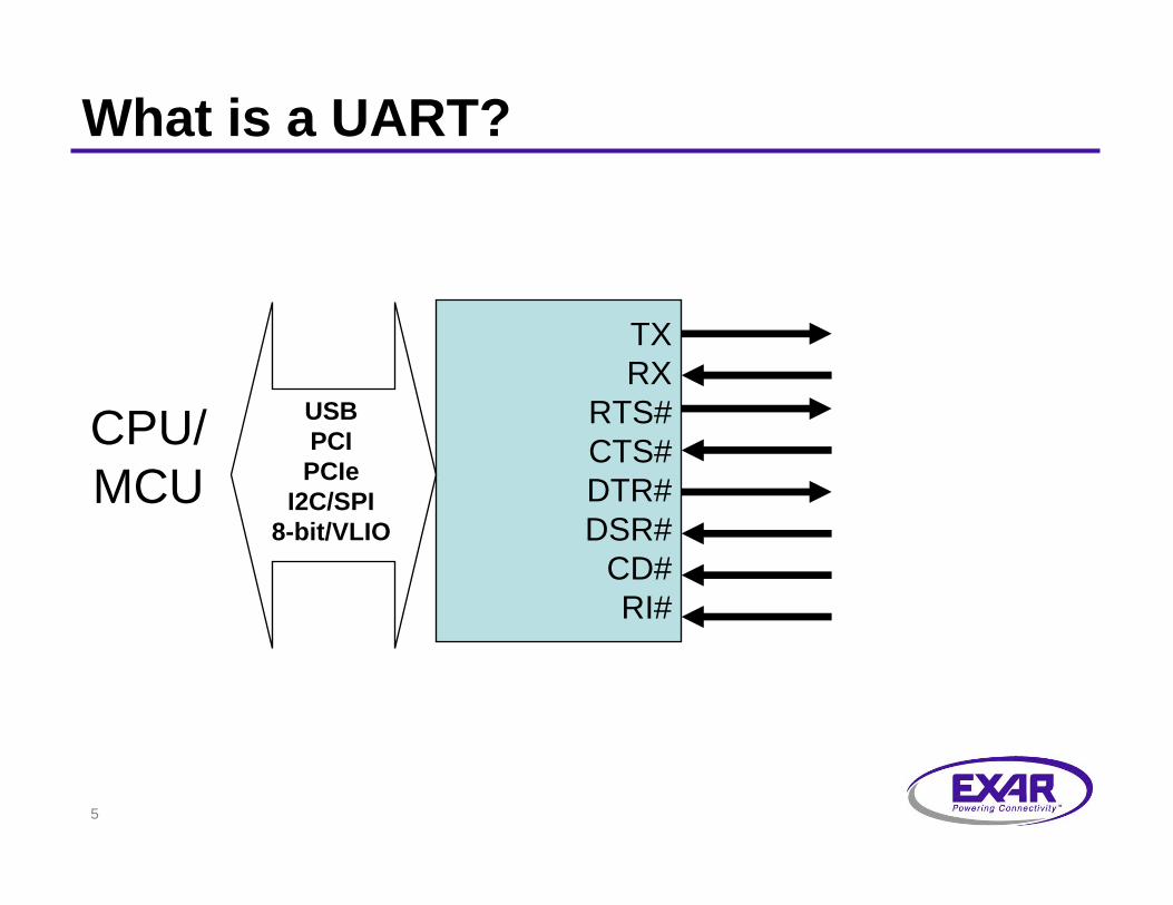
What is a UART?
TXRX
RTS#CTS#DTR#DSR#
CD#RI#
CPU/MCU
USBPCI
PCIeI2C/SPI
8-bit/VLIO

6
UART Block Diagram
CPU Interface
BRG Transmitter
Receiver
XTAL1XTAL2
16550UART
RegistersModem
I/OSignals
TX
RX
RTS#CTS#DTR#DSR#CD#RI#
InterruptINT
7
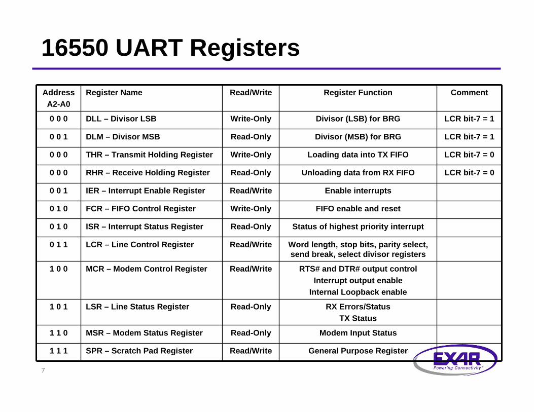
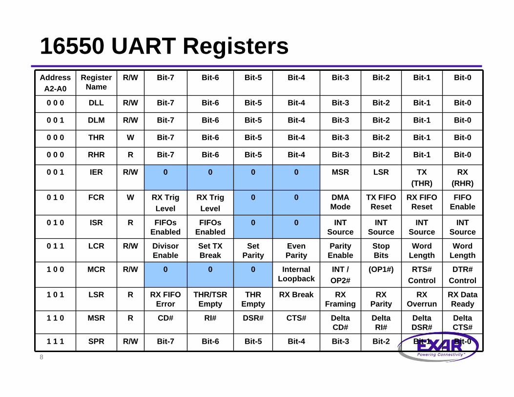
16550 UART RegistersAddress
A2-A0Register Name Read/Write Register Function Comment
0 0 0 DLL – Divisor LSB Write-Only Divisor (LSB) for BRG LCR bit-7 = 1
0 0 1 DLM – Divisor MSB Read-Only Divisor (MSB) for BRG LCR bit-7 = 1
0 0 0 THR – Transmit Holding Register Write-Only Loading data into TX FIFO LCR bit-7 = 0
0 0 0 RHR – Receive Holding Register Read-Only Unloading data from RX FIFO LCR bit-7 = 0
0 0 1 IER – Interrupt Enable Register Read/Write Enable interrupts
0 1 0 FCR – FIFO Control Register Write-Only FIFO enable and reset
0 1 0 ISR – Interrupt Status Register Read-Only Status of highest priority interrupt
0 1 1 LCR – Line Control Register Read/Write Word length, stop bits, parity select, send break, select divisor registers
1 0 0 MCR – Modem Control Register Read/Write RTS# and DTR# output controlInterrupt output enable
Internal Loopback enable
1 0 1 LSR – Line Status Register Read-Only RX Errors/StatusTX Status
1 1 0 MSR – Modem Status Register Read-Only Modem Input Status
1 1 1 SPR – Scratch Pad Register Read/Write General Purpose Register
8
16550 UART RegistersAddress
A2-A0Register
NameR/W Bit-7 Bit-6 Bit-5 Bit-4 Bit-3 Bit-2 Bit-1 Bit-0
0 0 0 DLL R/W Bit-7 Bit-6 Bit-5 Bit-4 Bit-3 Bit-2 Bit-1 Bit-0
0 0 1 DLM R/W Bit-7 Bit-6 Bit-5 Bit-4 Bit-3 Bit-2 Bit-1 Bit-0
0 0 0 THR W Bit-7 Bit-6 Bit-5 Bit-4 Bit-3 Bit-2 Bit-1 Bit-0
0 0 0 RHR R Bit-7 Bit-6 Bit-5 Bit-4 Bit-3 Bit-2 Bit-1 Bit-0
0 0 1 IER R/W 0 0 0 0 MSR LSR TX(THR)
RX(RHR)
0 1 0 FCR W RX TrigLevel
RX TrigLevel
0 0 DMA Mode
TX FIFO Reset
RX FIFO Reset
FIFO Enable
0 1 0 ISR R FIFOsEnabled
FIFOsEnabled
0 0 INT Source
INT Source
INT Source
INT Source
0 1 1 LCR R/W Divisor Enable
Set TX Break
Set Parity
Even Parity
Parity Enable
Stop Bits
Word Length
Word Length
1 0 0 MCR R/W 0 0 0 Internal Loopback
INT /OP2#
(OP1#) RTS#Control
DTR#Control
1 0 1 LSR R RX FIFO Error
THR/TSR Empty
THR Empty
RX Break RX Framing
RX Parity
RX Overrun
RX Data Ready
1 1 0 MSR R CD# RI# DSR# CTS# Delta CD#
Delta RI#
Delta DSR#
Delta CTS#
1 1 1 SPR R/W Bit-7 Bit-6 Bit-5 Bit-4 Bit-3 Bit-2 Bit-1 Bit-0

9
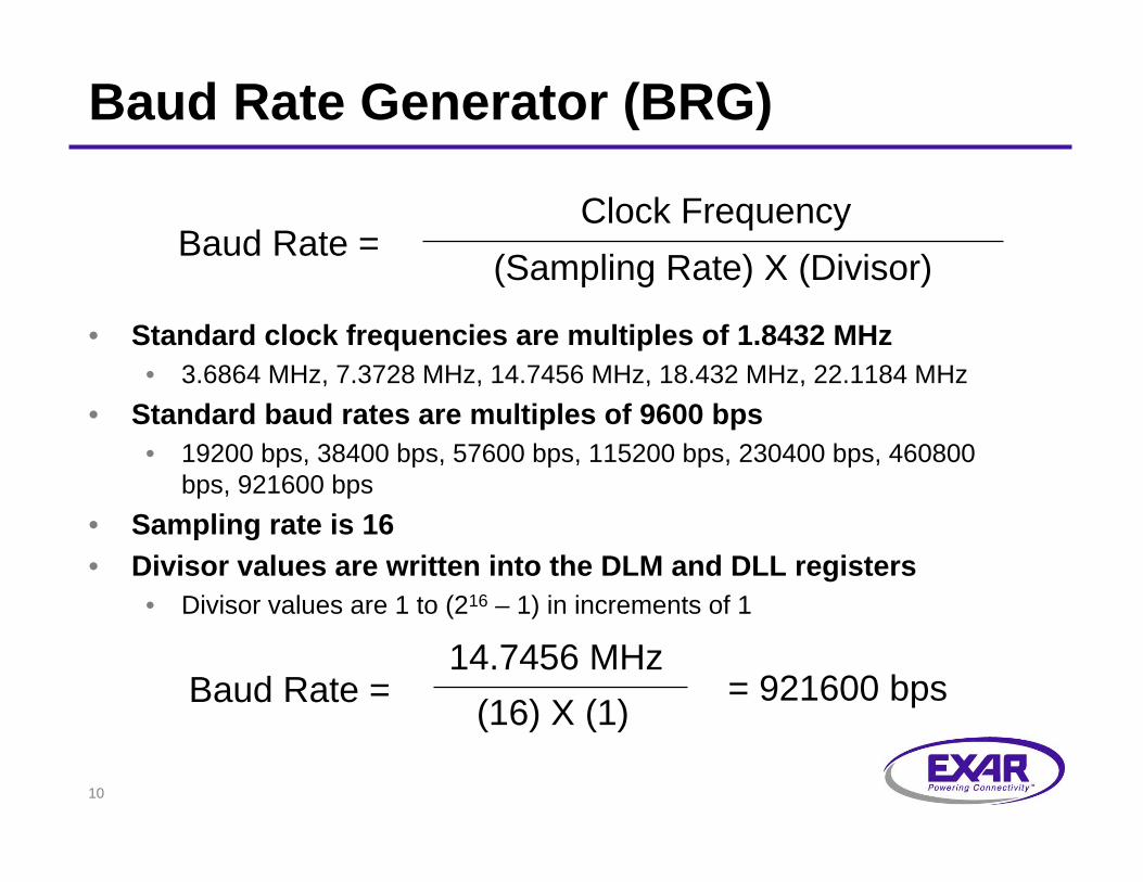
Baud Rate Generator (BRG)
• Used to generate the baud rates for both the transmitter and receiver
• Not required for any other function including reads and writes
• Crystal or External Clock• 16-bit divisor programmed in DLM/DLL
registers
10
Baud Rate Generator (BRG)
Baud Rate =Clock Frequency
(Sampling Rate) X (Divisor)
• Standard clock frequencies are multiples of 1.8432 MHz• 3.6864 MHz, 7.3728 MHz, 14.7456 MHz, 18.432 MHz, 22.1184 MHz
• Standard baud rates are multiples of 9600 bps• 19200 bps, 38400 bps, 57600 bps, 115200 bps, 230400 bps, 460800
bps, 921600 bps• Sampling rate is 16• Divisor values are written into the DLM and DLL registers
• Divisor values are 1 to (216 – 1) in increments of 1
Baud Rate =14.7456 MHz
(16) X (1)= 921600 bps

11
Transmitter
• Parallel-to-serial conversion• Non-FIFO Mode
• Transmit Holding Register (THR) and Transmit Shift Register (TSR)
• FIFO Mode• Transmit (TX) FIFO and Transmit Shift Register
(TSR)• 16X timing for bit shifting• Character Framing• Parity Insertion• TX FIFO interrupt and status
12
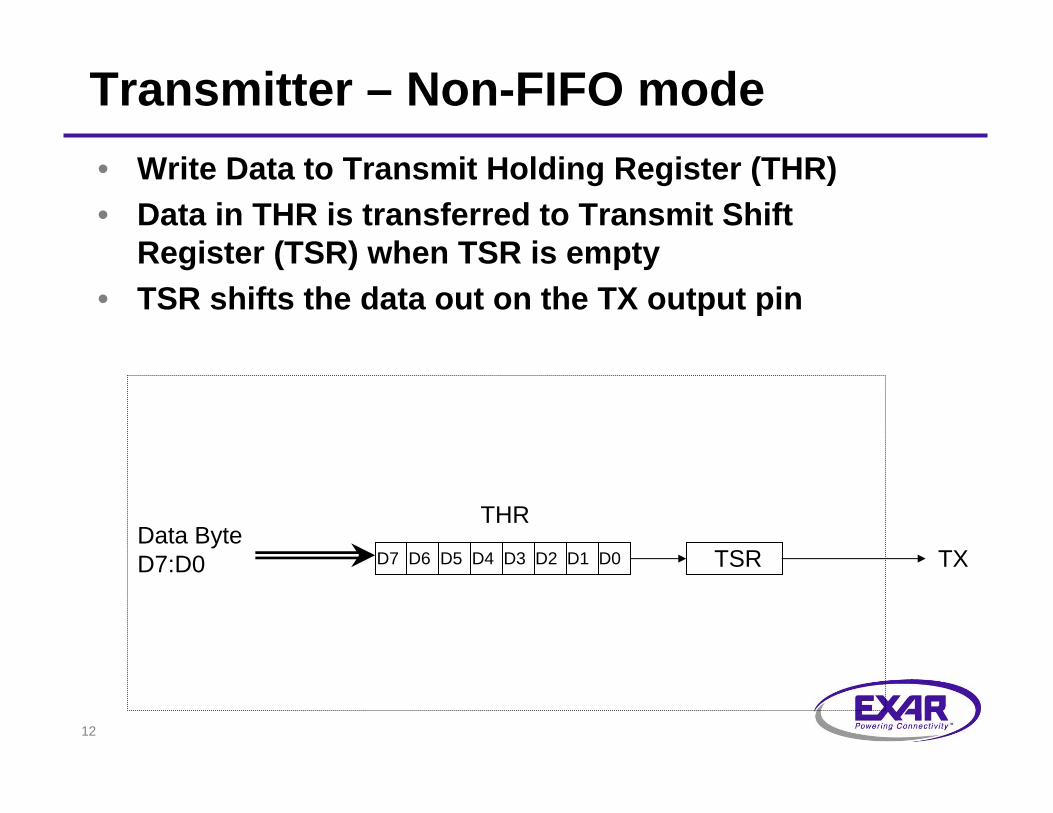
Transmitter – Non-FIFO mode
THR
TSRD7 D6 D5 D4 D3 D2 D1 D0 TXData Byte D7:D0
• Write Data to Transmit Holding Register (THR)• Data in THR is transferred to Transmit Shift
Register (TSR) when TSR is empty• TSR shifts the data out on the TX output pin
13
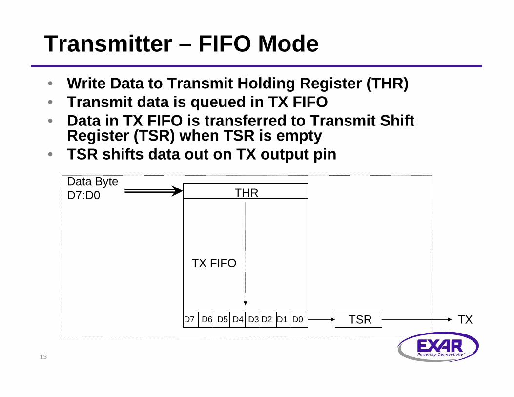
Transmitter – FIFO Mode
THR
TX FIFO
TSRD7 D6 D5 D4 D3 D2 D1 D0 TX
Data Byte D7:D0
• Write Data to Transmit Holding Register (THR)• Transmit data is queued in TX FIFO• Data in TX FIFO is transferred to Transmit Shift
Register (TSR) when TSR is empty• TSR shifts data out on TX output pin
14
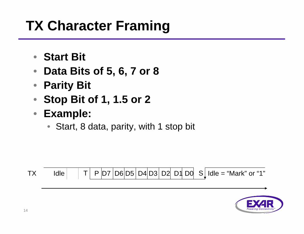
TX Character Framing
• Start Bit• Data Bits of 5, 6, 7 or 8• Parity Bit• Stop Bit of 1, 1.5 or 2• Example:
• Start, 8 data, parity, with 1 stop bit
SD7 D6 D5 D4 D3 D2 D1 D0T Idle = “Mark” or “1”TX PIdle
15
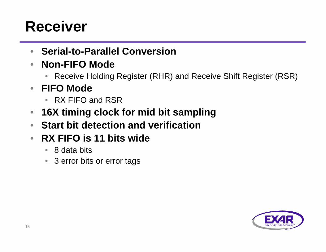
Receiver• Serial-to-Parallel Conversion• Non-FIFO Mode
• Receive Holding Register (RHR) and Receive Shift Register (RSR)• FIFO Mode
• RX FIFO and RSR• 16X timing clock for mid bit sampling • Start bit detection and verification• RX FIFO is 11 bits wide
• 8 data bits• 3 error bits or error tags

16
Receiver – Non-FIFO Mode
RSR RX
Error Tags RHR
Data Byte D7:D0
D7 D6 D5 D4 D3 D2 D1 D0B F P
• Incoming data is received in the Receive Shift Register (RSR)• Received data is transferred to the RHR• Error tags associated with data in RHR can be read via LSR• Read RHR to read the data out
17
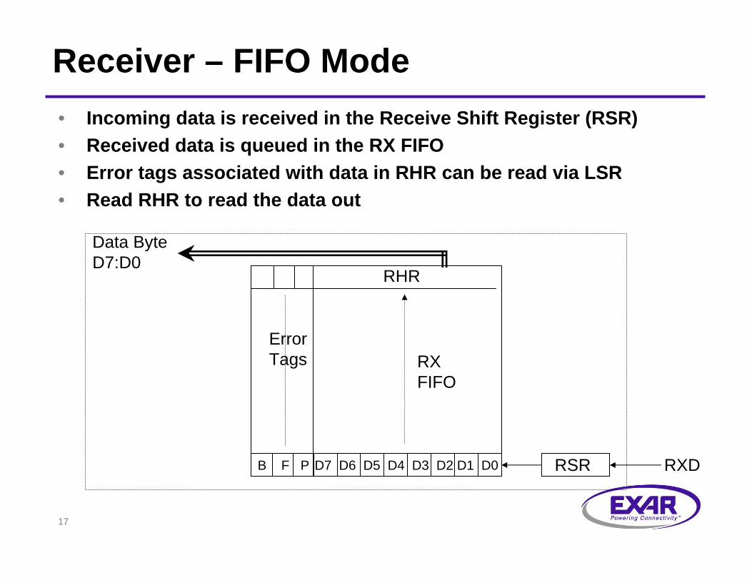
Receiver – FIFO Mode
RX FIFO
RSR RXD
Error Tags
RHR
Data Byte D7:D0
D7 D6 D5 D4 D3 D2 D1 D0B F P
• Incoming data is received in the Receive Shift Register (RSR)• Received data is queued in the RX FIFO• Error tags associated with data in RHR can be read via LSR• Read RHR to read the data out

18
RX Character Validation
• Start bit detection and validation• HIGH to LOW transition indicates a start bit• Start bit validated if RX input is still LOW during
mid bit sampling• Data, parity and stop bits are sampled at mid bit• A valid stop bit is HIGH when the stop bit is
sampled
SD7 D6 D5 D4 D3 D2 D1 D0T Idle = “Mark” or “1” RXPIdle

19
RX Error Reporting
• Line Status errors • Error tags are associated with each byte
• Framing error if stop bit is not detected• Parity error if parity bit is incorrect• Break detected if RX input is LOW for duration of one
character time and stop bit is not detected• Overrun error if character is received in RSR when
RX FIFO is full• Non-FIFO mode
• RHR has a data byte and data received in RSR• RSR data overwrites RHR data
• FIFO mode• RX FIFO is full and data is received in RSR• Data in RX FIFO is not overwritten by data in RSR
20
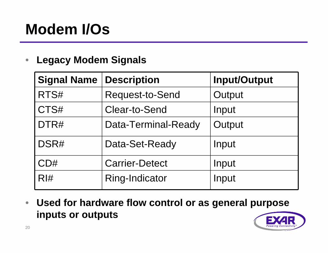
Modem I/Os
• Legacy Modem Signals
• Used for hardware flow control or as general purpose inputs or outputs
Signal Name Description Input/OutputRTS# Request-to-Send OutputCTS# Clear-to-Send InputDTR# Data-Terminal-Ready Output
DSR# Data-Set-Ready Input
CD# Carrier-Detect InputRI# Ring-Indicator Input
21
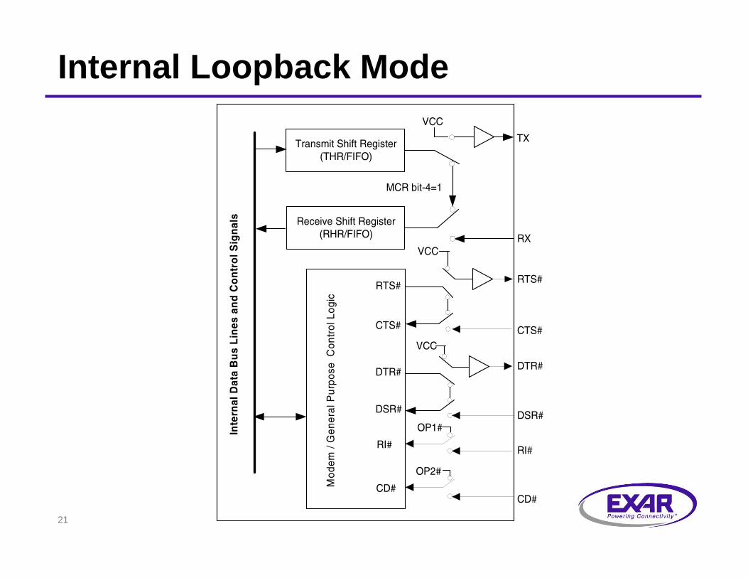
Internal Loopback Mode
TX
RX
Mod
em /
Gen
eral
Pur
pose
Con
trol
Log
ic
Inte
rnal
Dat
a B
us
Lin
es a
nd
Co
ntr
ol S
ign
als
RTS#
MCR bit-4=1
VCC
VCC
Transmit Shift Register(THR/FIFO)
Receive Shift Register(RHR/FIFO)
CTS#
DTR#
DSR#
RI#
CD#
OP1#
RTS#
CTS#
DTR#
DSR#
RI#
CD#
VCC
OP2#

22
Interrupts
• Interrupt Source Register (ISR)• If there are multiple interrupts, ISR reports only the highest pending
interrupt• Lower priority interrupts will be reported when higher priority
interrupts are cleared
Priority Level
ISR bit-3
ISR bit-2
ISR bit-1
ISR bit-0
Source of Interrupt
1 0 1 1 0 LSR (RX Data Error)2 1 1 0 0 RXRDY (RX Data Time-out)3 0 1 0 0 RXRDY (RX Data Ready)4 0 0 1 0 TXRDY (TX Empty)5 0 0 0 0 MSR (Modem Status)- 0 0 0 1 None

E-mail hotline: [email protected]