Embed Size (px)
Citation preview
Accelerating the next technology revolution
Copyright ©2009SEMATECH, Inc. SEMATECH, and the SEMATECH logo are registered servicemarks of SEMATECH, Inc. International SEMATECH Manufacturing Initiative, ISMI, Advanced Materials Research Center and AMRC are servicemarks of SEMATECH, Inc. All other servicemarks and trademarks are the property of their respective owners.
Understanding Chemical Interactions Between Thin Buried Layers of Microelectronic Materials in Advanced CMOS Structures
International Workshop for New Opportunities in Hard X-ray Photoelectron Spectroscopy: HAXPES 2009
Patrick S. Lysaght1, Joseph C. Woicik2, Daniel A. Fischer2, M. Alper Sahiner3
1SEMATECH, Austin TX
2National Institute of Standards and Technology, Gaithersburg, MD
3Seton Hall University, Physics Department, South Orange, NJ
2228 August 2009 2
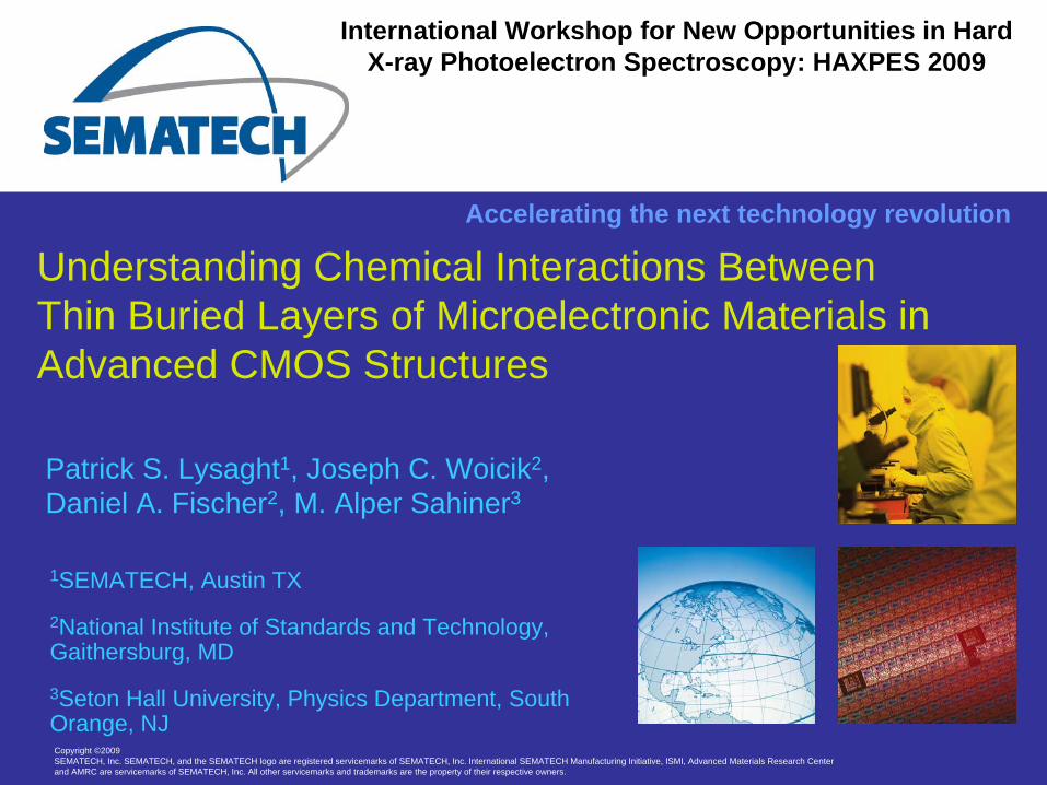
Outline
• Intro – About SEMATECH
• High-k/Metal Gate Scaling Trends
• More than Moore - Novel Structures & New Materials
• HAXPES Characterization – Practical Examples• High-k Integration - VKE-XPS: Si/SiOx /HfO2
• Dielectric Cap Layers: Higher-k & EWF Tuning
• Disruptive Technology – Toward Zero IF
• Flash Memory Retention - Impact of Intermixing
3
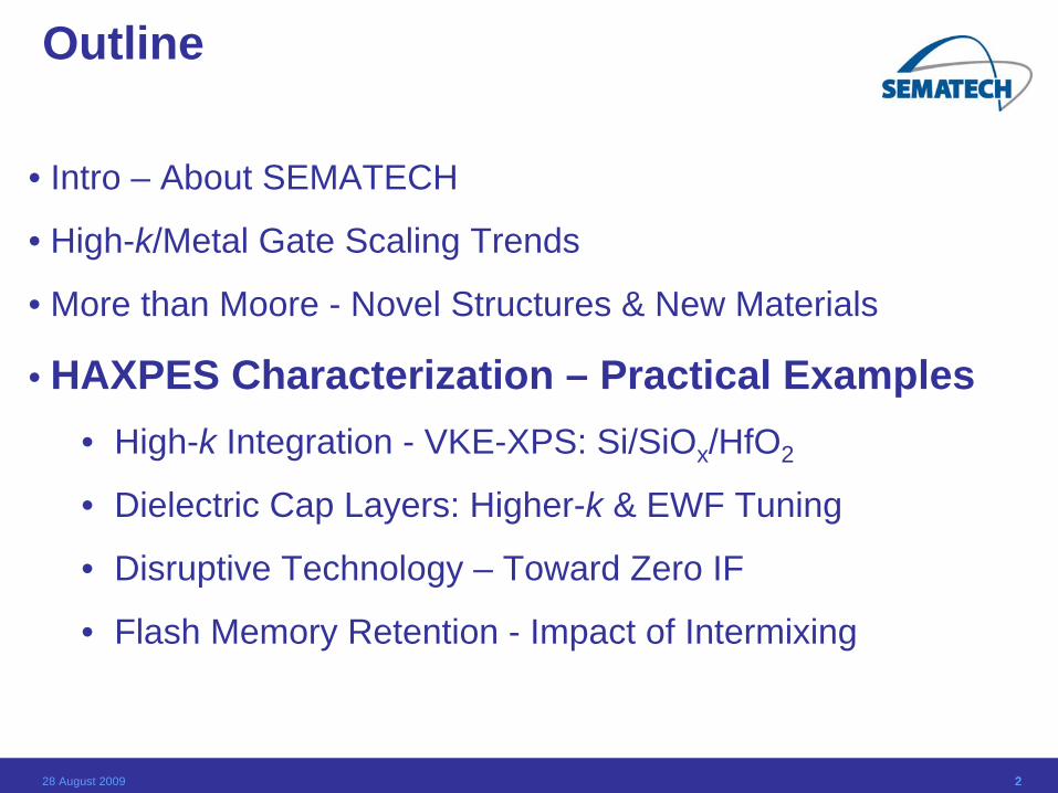
About SEMATECH…Global Consortium
SEMATECH Front End Processes (FEP) DivisionAdvanced Dielectrics & Electrodes for Logic & Memory
Advanced CMOS Scaling – Planar and Non-Planar
Electrical & Physical Characterization /Reliability & Metrology
Novel Emerging Technologies

4
SEMATECH Extensive R&D Network
• University Network: 80+ schools• Examples: MIT, Stanford, Berkeley,
UIUC, CMU, GATech, UT Austin• Students completed (or completing)
their PhD research: 27• Co-authored papers = 180+• Jointly arranged conferences,
workshops = 9
Albany, NY:SEMATECH North Funded by State of NYHome of Lithography, 3D Interconnect, Metrology and FEP
300,000 sq. ft. class 1 clean roomState of the art tools for 300 mm wafers
National Lab Network:• BNL Synchrotron XPS, XAS• LANL Neutron SANS, SPEAR• ORNL HR TEM• ANL Ferroelectric, piezoelectric• Sandia MEMS• NIST FTIR,1/f Noise, XRD
Austin, TX:SEMATECH corporate HQ Home of FEP, Emerging Technologies and ISMI
Premier user of 68,000 sq. ft. class 1 clean room for 200/300mm wafers
R&D of advanced materials/structuresHighly Productive Collaborations w/NIST Scientists,
Joe Woicik & Dan Fischer at NSLS/BNL
5
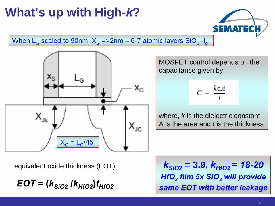
XG = LG /45
When LG scaled to 90nm, XG =>2nm – 6-7 atomic layers SiO2 -Ig
MOSFET control depends on the capacitance given by:
where, k is the dielectric constant, A is the area and t is the thickness
What’s up with High-k?
kSiO2 = 3.9, kHfO2 = 18-20HfO2
film 5x SiO2
will provide same EOT with better leakage EOT = (kSiO2 /kHfO2
)tHfO2
equivalent oxide thickness (EOT) :
6
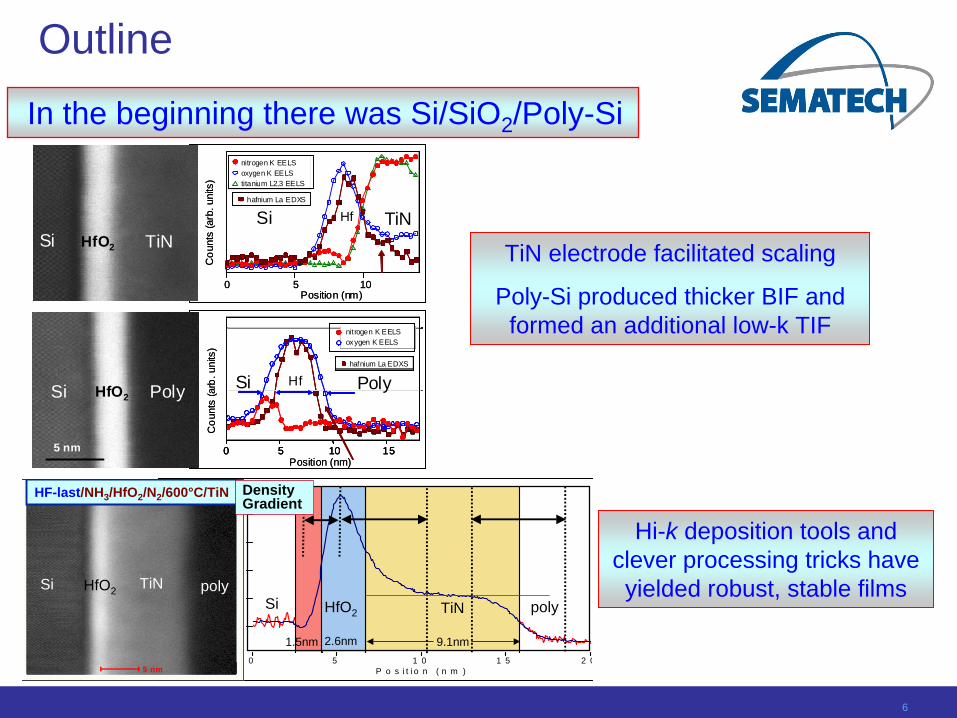
OutlineIn the beginning there was Si/SiO2 /Poly-Si
Position (nm)1050
nitrogen K EELS oxygen K EELS titanium L2,3 EELS
Cou
nts
(arb
. uni
ts)
hafnium La EDXS
Position (nm)1050
nitrogen K EELS oxygen K EELS titanium L2,3 EELS
Cou
nts
(arb
. uni
ts)
hafnium La EDXShafnium La EDXS
Position (nm)
Cou
nts
(arb
. uni
ts)
151050
nitrogen K EELS oxygen K EELS
hafnium La EDXS
Position (nm)
Cou
nts
(arb
. uni
ts)
151050
nitrogen K EELS oxygen K EELS
hafnium La EDXS
151050
nitrogen K EELS oxygen K EELS nitrogen K EELS oxygen K EELS
hafnium La EDXShafnium La EDXS
Si Poly
Si TiN
Hf
Hf
5 nm
Si TiN
Si PolyHfO2
HfO2
P o s i t i o n ( n m )
Cou
nts
2 01 51 050
3 5 0 0 0
3 0 0 0 0
2 5 0 0 0
2 0 0 0 0
1 5 0 0 0
1 0 0 0 0
5 nm
HF-last/NH3/HfO2/N2/600°C/TiN
1.5nm 2.6nm 9.1nm
Si TiNSi HfO2
HfO2
polypoly
TiN
Density Gradient
TiN electrode facilitated scaling
Poly-Si produced thicker BIF and formed an additional low-k TIF
Hi-k deposition tools and clever processing tricks have yielded robust, stable films
7
50 nm50 nm~32nm
50 nm50 nm~32nm
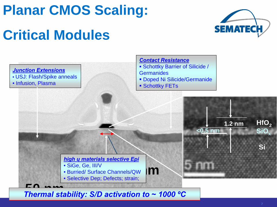
Thermal stability: S/D activation to ~ 1000 ºC
high ų
materials
selective Epi• SiGe, Ge, III/V• Burried/ Surface Channels/QW• Selective Dep; Defects; strain;
Junction Extensions• USJ: Flash/Spike anneals• Infusion, Plasma
Contact Resistance
Schottky Barrier of Silicide / Germanides Doped Ni Silicide/Germanide Schottky FETs
Si
HfO2SiOx
1.2 nm<0.5 nm
Planar CMOS Scaling:
Critical Modules
8
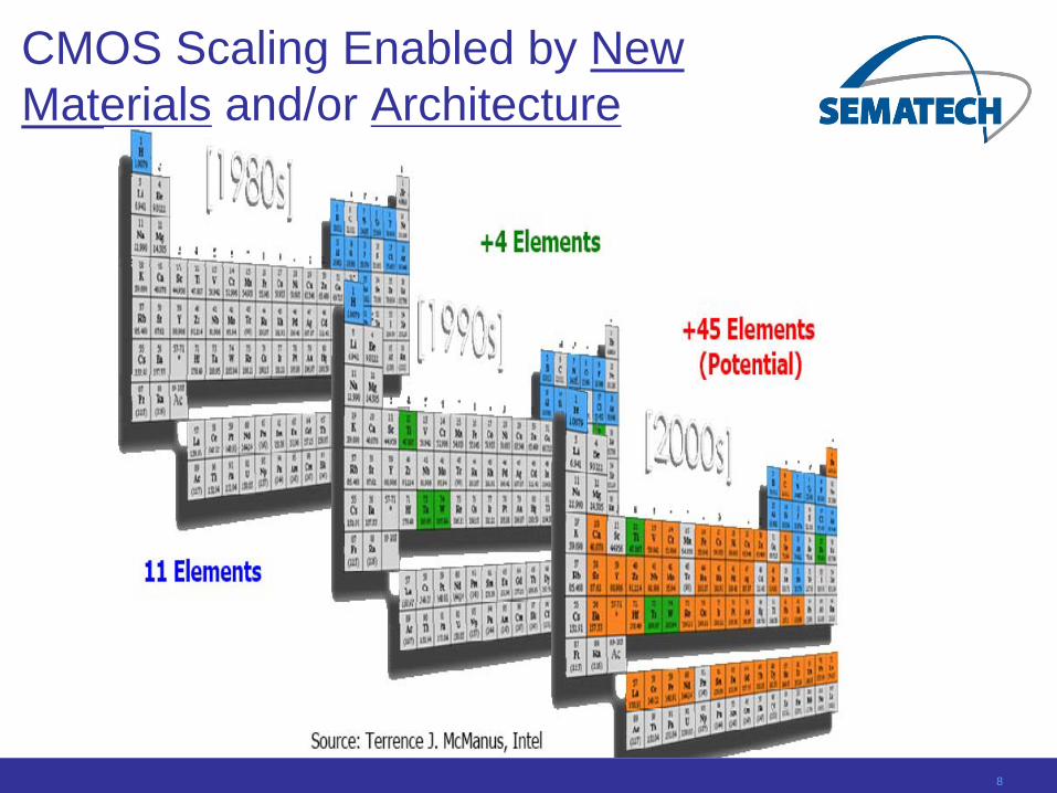
CMOS Scaling Enabled by New Materials and/or Architecture
9
Img: 'E0318 071221011_7071107_10_GJ2_rot_s.dm3' MAG: 49kX
50 nm50 nm~32nm
Img: 'E0318 071221011_7071107_10_GJ2_rot_s.dm3' MAG: 49kX
50 nm50 nm~32nm
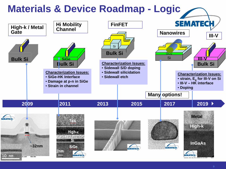
Materials & Device Roadmap - Logic
2009
High-k / Metal Gate
FinFET
2011 2013 2015 2017 2019
Bulk SiBulk Si
SiGeBulk SiIII-V
Hi Mobility Channel
Si
Bulk Si
(b)
r ans i s tor _200_T aN _Z r O_ InGaAs .Ed_r ot_s .dm3' M AG:
Metal
High-k
InGaAs
Characterization Issues:• SiGe-HK Interface• Damage at p-n in SiGe• Strain in channel
SiO2Si
Nanowires III-V
Many options!
Characterization Issues:• Sidewall S/D doping• Sidewall silicidation• Sidewall etch
Characterization Issues:• strain, Eg for III-V on Si• III-V – HK interface• Doping

10
Materials & Device Roadmap -Memory
2009 2011 2013 2015 2017 2019
SiN Trap Flash
SMSG 2008 IEDM
50nm
300A SiN
2nm
Metal Nanocrystal Flash
Many options:• Resistance Change• Molecular• Spin Torque
1T1C Issues:• HK/MG interface• HK/MG crystal
1T Issues:•Charge storage•Etch damage•Junction quality
-
SiO2
SiNx
TaN
Al2 O31C
1T
DRAM
Nanosys, Inc.
Characterization Issues:• Conduction mechanism• Oxygen Vacancies• NiO, TiO, WO, TaO
Characterization Issues:• traps, defects in Al2O3• Storage node: SiN -> metal NC• High work function metal
M
IM
RRAMR. Waser et al. Nature 2007
11 1128 August 2009 11
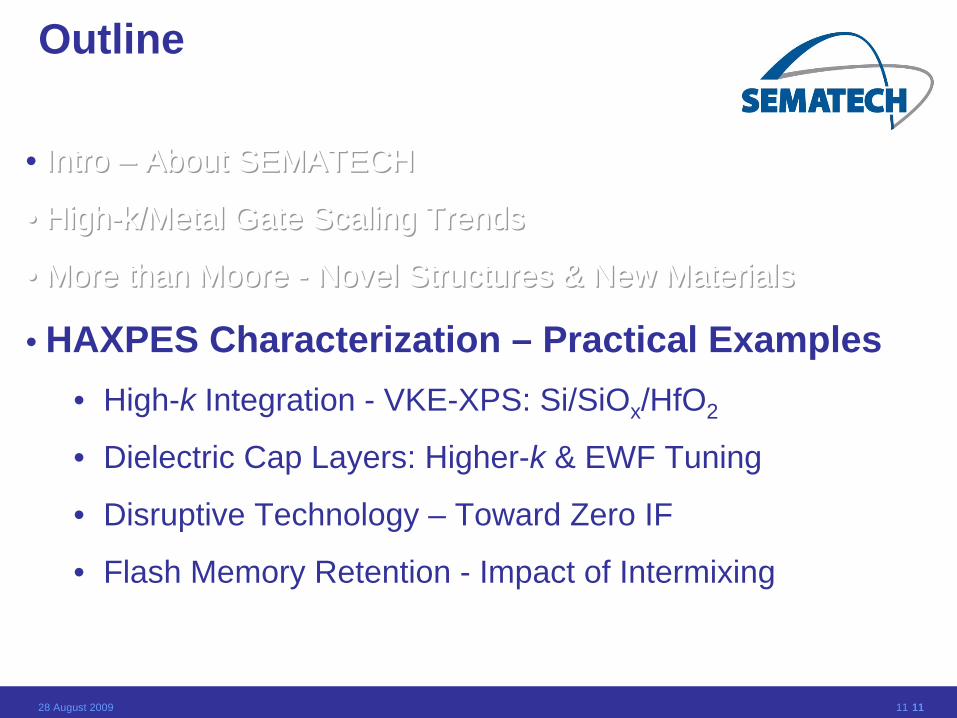
Outline
• Intro Intro Intro ––– About SEMATECHAbout SEMATECHAbout SEMATECH
••• HighHighHigh---k/Metal Gate Scaling Trends k/Metal Gate Scaling Trends k/Metal Gate Scaling Trends
••• More than Moore More than Moore More than Moore --- Novel Structures & New Materials Novel Structures & New Materials Novel Structures & New Materials
• HAXPES Characterization – Practical Examples• High-k Integration - VKE-XPS: Si/SiOx /HfO2
• Dielectric Cap Layers: Higher-k & EWF Tuning
• Disruptive Technology – Toward Zero IF
• Flash Memory Retention - Impact of Intermixing
12
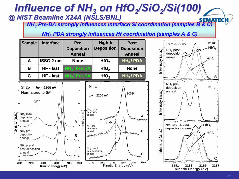
Influence of NHInfluence of NH33
on HfOon HfO22
/SiO/SiO22
/Si(100)/Si(100)
Si 2pNormalized to Si0
A
B
C
Kinetic Energy (eV)2103
Inte
nsity
(a.u
.)
21012099209720952093
Si4+
Si 2pNormalized to Si0
A
B
C
Kinetic Energy (eV)2103
Inte
nsity
(a.u
.)
21012099209720952093
Si4+
hv = 2200 eV
NH3 post-deposition anneal
NH3 pre-deposition anneal
NH3 pre- & post-deposition anneal
NH3 Pre-DA strongly influences interface Si coordination (samples B & C)
NH3 PDA strongly influences Hf coordination (samples A & C)
@ NIST Beamline X24A (NSLS/BNL)@ NIST Beamline X24A (NSLS/BNL)
A
21872181 2183 2185Kinetic Energy (eV)
Hf 4fHfO2
Inte
nsity
(a.u
.)In
tens
ity (a
.u.)
Inte
nsity
(a.u
.)
NH3 pre-deposition anneal
NH3 post-deposition anneal
B
C
NH3 pre- & post-deposition anneal
HfO2
HfO2
Hf-N
Hf-N
hv = 2200 eVHigh-k Deposition
A ISSG 2 nm None HfO2 NH3 / PDA
B HF - last NH3 / Pre-DA HfO2 None
C HF - last NH3 / Pre-DA HfO2 NH3 / PDA
Sample Interface Pre Deposition
Anneal
Post Deposition
Anneal
High-k Deposition
A ISSG 2 nm None HfO2 NH3 / PDA
B HF - last NH3 / Pre-DA HfO2 None
C HF - last NH3 / Pre-DA HfO2 NH3 / PDA
Sample Interface Pre Deposition
Anneal
Post Deposition
Anneal
1799 1781 1783 1805 1807
N 1sHf-N
1809
Hf-N
A
B
C
Si-N
Kinetic Energy (eV)
Inte
nsity
(a.u
.)
hv = 2200 eV
NH3 pre-deposition anneal
NH3 pre- & post-deposition anneal
NH3 post-deposition anneal
13
HAXPES: VKE-XPS Depth ProfilingVariable Kinetic Energy-XPS: Si 1s BE as f(depth) through the IF
Hf 4f B.E. constant surface & interface, Oxygen deficient Si, at the SiO2 /HfO2 IF
Inte
nsity
(a.u
.)
Sample A
Nor
mal
ized
Inte
nsity
( arb
. uni
ts)
Kinetic Energy (E-Ec)0 2 4-2-4-6-8
Si 1s
moreoxidized
less oxidized
moreoxidized
less oxidized
“Interface effect”hv=2100 eV
hv=2500 eV
hv=2600 eV
hv=3000 eV
hv=3500 eV
3 nm HfO2
Si
2nm SiO2
P. S. Lysaght, J. C. Woicik, D. A. Fischer, G. I. Bersuker, H-H. Tseng, and R. Jammy, J. Appl. Phys. 101, 024105 (2007).
hv ~ 2170 eV
Sample A
80º - surface sensitive
Glancing -interface sensitive
2179 2181 2183 2185 2187
Hf 4 f
Kinetic Energy (eV)
NH3 Post Deposition Anneal only
hv = 2200 eV
@ NIST Beamline X24A (NSLS/BNL)
Variable Kinetic Energy –1)Depth profile2)Avoid Auger interference3)Capture higher BE surface sensitive core lines to compare with bulk sensitive
14
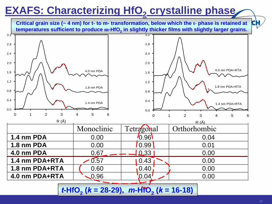
R (Å)
0 1 2 3 4 5 60.0
0.4
0.8
1.2
1.6
2.0
2.4
2.8
3.2
1.4 nm PDA
1.8 nm PDA
4.0 nm PDA
R (Å)
0 1 2 3 4 5 60.0
0.4
0.8
1.2
1.6
2.0
2.4
2.8
3.2
1.4 nm PDA+RTA
4.0 nm PDA+RTA
1.8 nm PDA+RTA
Monoclinic Tetragonal Orthorhombic 1.4 nm PDA 0.00 0.96 0.04 1.8 nm PDA 0.00 0.99 0.01 4.0 nm PDA 0.67 0.33 0.00 1.4 nm PDA+RTA 0.57 0.43 0.00 1.8 nm PDA+RTA 0.60 0.40 0.00 4.0 nm PDA+RTA 0.96 0.04 0.00
Critical grain size (~ 4 nm) for t- to m- transformation, below which the t- phase is retained at temperatures sufficient to produce m-HfO2 in slightly thicker films with slightly larger grains.
t-HfO2 (k
= 28-29), m-HfO2 (k
= 16-18)
EXAFS: Characterizing HfO2 crystalline phase
15 15
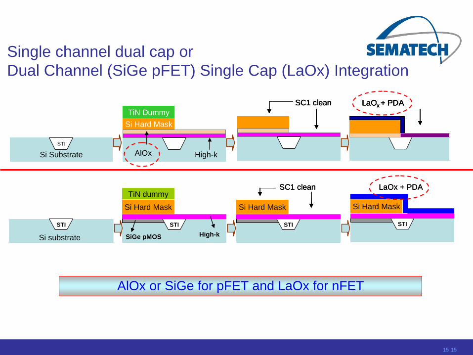
Single channel dual cap or Dual Channel (SiGe pFET) Single Cap (LaOx) Integration
AlOx or SiGe for pFET and LaOx for nFET
Si SubstrateSTI
Si SubstrateSTI
Si Hard MaskTiN Dummy
High-kAlOx
Si Hard MaskTiN Dummy
High-kAlOx
SC1 cleanSC1 clean LaOx + PDA (Optional)LaOx + PDA (Optional)
Si SubstrateSTI
Si SubstrateSTI
Si Hard MaskTiN Dummy
High-kAlOx
Si Hard MaskTiN Dummy
High-kAlOx
SC1 cleanSC1 clean LaOx + PDA (Optional)LaOx + PDA (Optional)LaOx + PDA (Optional)LaOx + PDA (Optional)
STI
Si substrate
STI
SiGe pMOS High-k
Si Hard MaskTiN dummy
STI
Si Hard Mask
SC1 clean
STI
Si Hard Mask
LaOx + PDA
STI
Si substrate
STI
Si substrate
STI
SiGe pMOS High-k
Si Hard MaskTiN dummy
STI
SiGe pMOS High-k
Si Hard MaskTiN dummy
STI
Si Hard Mask
SC1 clean
STI
Si Hard Mask
SC1 clean
STI
Si Hard Mask
LaOx + PDA
STI
Si Hard Mask
LaOx + PDA

16
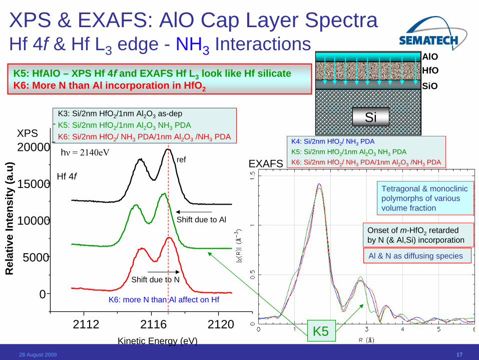
XPS & EXAFS: AlO Cap Layer Spectra Hf 4f & Hf L3 edge - N2 Interactions
AlO
Si
SiOHfO
N2 PDA forms stable m-HfO2 – wrt Al diffusion
2- 2nm HfO2/N2 PDA (reference)5- 2nm HfO2/N2 PDA/ 1nm Al2O3/N2 PDA11- 2nm HfO2/ 1nm Al2O3/ N2 PDA
m-HfO2 results when pre-annealed via N2 PDA
m-HfO2
EXAFS
: HfO2/N2 PDA
2- 2nm HfO2/N2 PDA (reference)5- 2nm HfO2/N2 PDA/ 1nm Al2O3/N2 PDA11- 2nm HfO2/ 1nm Al2O3/ N2 PDA
2152 2156 2160 21640
5000
10000
15000
20000
Kinetic Energy (eV)
Shift due to Al
No HfO2 pre-anneal
Hf4f
slight Al shift
Rel
ativ
e In
tens
ity (a
.u.)
hν
= 2170eV
2- 2nm HfO2 /N2 PDA (reference)5- 2nm HfO2 /N2 PDA/ 1nm Al2 O3 /N2 PDA11- 2nm HfO2 / 1nm Al2 O3 /N2 PDA
11not m-HfO2
171728 August 2009 17
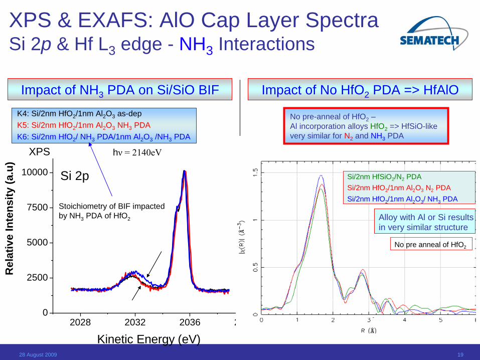
K4: Si/2nm HfO2/ NH3 PDAK5: Si/2nm HfO2/1nm Al2O3 NH3 PDAK6: Si/2nm HfO2/ NH3 PDA/1nm Al2O3 /NH3 PDA
Onset of m-HfO2 retarded by N (& Al,Si) incorporation
Tetragonal & monoclinic polymorphs of various volume fraction
AlO
Si
SiOHfO
Al & N as diffusing species
K5: HfAlO – XPS Hf 4f
and EXAFS Hf L3 look like Hf silicate K6: More N than Al incorporation in HfO2
Hf 4f
Shift due to Al
Shift due to N
ref
K6: more N than Al affect on Hf
EXAFS
XPS
XPS & EXAFS: AlO Cap Layer Spectra Hf 4f & Hf L3 edge - NH3 Interactions
K52112 2116 2120
0
5000
10000
15000
20000
Inte
nsity
(cps
)
Kinetic Energy (eV)
K3: Si/2nm HfO2 /1nm Al2 O3 as-depK5: Si/2nm HfO2 /1nm Al2 O3 NH3 PDAK6: Si/2nm HfO2 / NH3 PDA/1nm Al2 O3 /NH3 PDA
Rel
ativ
e In
tens
ity (a
.u)
hν
= 2140eV
181828 August 2009 18
K4: Si/2nm HfO2 /1nm Al2 O3 as-depK5: Si/2nm HfO2 /1nm Al2 O3 NH3 PDAK6: Si/2nm HfO2 / NH3 PDA/1nm Al2 O3 /NH3 PDA
AlN
N 1s
1720 1740 17600
4000
8000
12000
Inte
nsity
(cps
)
Kinetic Energy (eV)
k4 k5 k6
Hf4p3/2
~380eV BE
N-O N-O3
AlO
Si
SiOHfO
XPS & XAS: AlO Cap Layer Spectra N 1s & N K1 edge - NH3 Interactions
390 400 410 420 430 440
0.0
0.2
0.4
0.6
0.8
1.0
K5 K6
Inte
nsity
(cps
)
Energy (eV)
Al-N
Hf-N
N K-edge absorption
Low E XASXPS
K6
Al cap more easily etched if HfO2 is pre-annealed
Rel
ativ
e In
tens
ity (a
.u)
hν
= 2140eV
1928 August 2009
K4: Si/2nm HfO2 /1nm Al2 O3 as-depK5: Si/2nm HfO2 /1nm Al2 O3 NH3 PDAK6: Si/2nm HfO2 / NH3 PDA/1nm Al2 O3 /NH3 PDA
2028 2032 2036 20400
2500
5000
7500
10000
Inte
nsity
(cps
)
Kinetic Energy (eV)
k4 k5 k6
Si 2p
Stoichiometry of BIF impacted by NH3 PDA of HfO2
No pre-anneal of HfO2 – Al incorporation alloys HfO2 => HfSiO-like very similar for N2 and NH3 PDA
XPS & EXAFS: AlO Cap Layer Spectra Si 2p & Hf L3 edge - NH3 Interactions
Impact of NH3 PDA on Si/SiO BIF
XPS
Impact of No HfO2 PDA => HfAlO
EXAFSSi/2nm HfSiO2/N2 PDASi/2nm HfO2/1nm Al2O3 N2 PDASi/2nm HfO2/1nm Al2O3/ NH3 PDA
Alloy with Al or Si results in very similar structure
No pre anneal of HfO2
Rel
ativ
e In
tens
ity (a
.u)
hν
= 2140eV

20
2060 2070 2080 2090 2100 2110 2120
0
2000
4000
6000
8000
10000
12000
14000In
tens
ity (a
.u.)
Kinetic Energy (eV)
asdep 700 950
2094 2096 2098 2100 2102 2104 21060
500
1000
1500
2000
2500
Inte
nsity
(a.u
.)Kinetic Energy (eV)
asdep 700 950
2070 2071 2072 2073 2074 2075400
600
800
1000
1200
1400
1600
1800
2000
Inte
nsity
(a.u
.)
Kinetic Energy (eV)
asdep 700 950
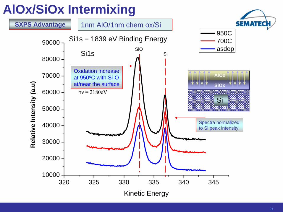
Shallow cores normalized to Si0, intensity & energy
Al2p
Si2p 4+
Si
SiOx
AlOx
AlOx/SiOx Intermixing1nm AlO/1nm chem ox/Si
Si0
21
1nm AlO/1nm chem ox/Si
320 325 330 335 340 34510000
20000
30000
40000
50000
60000
70000
80000
90000
Inte
nsity
(a.u
.)
Kinetic Energy
950C 700C asdep
Si1s
Si1s = 1839 eV Binding Energy
Si
SiOx
AlOx
SiSiO
Oxidation increase at 950ºC with Si-O at/near the surface
Spectra normalized to Si peak intensity
SXPS AdvantageR
elat
ive
Inte
nsity
(a.u
)
hν
= 2180eV
AlOx/SiOx Intermixing
22
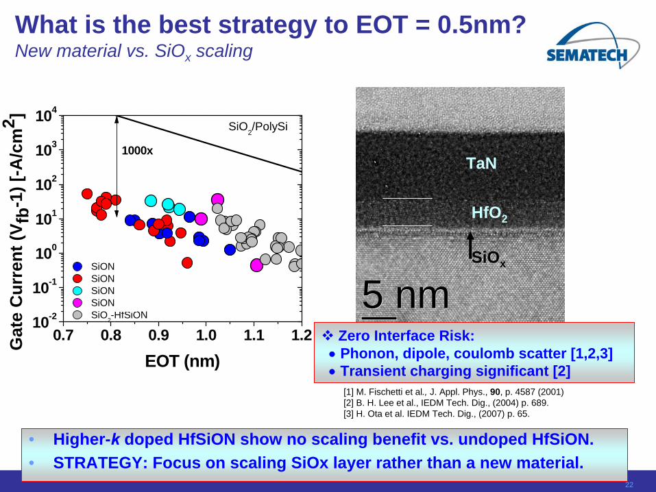
What is the best strategy to EOT = 0.5nm? New material vs. SiOx scaling
• Higher-k
doped HfSiON show no scaling benefit vs. undoped HfSiON.• STRATEGY: Focus on scaling SiOx layer rather than a new material.
0.7 0.8 0.9 1.0 1.1 1.210-2
10-1
100
101
102
103
104
SiON-HfTiSiON SiON-HfOx/HfZrOx/HfSiON SiON-HfSrSiON SiON-HfBiSiON SiO2-HfSiON
SiO2/PolySi
Gat
e C
urre
nt (V
fb-1
) [-A
/cm
2 ]
EOT (nm)
1000x
5 nm5 nm
TaN
HfO2
SiOx
Zero Interface Risk:
Phonon, dipole, coulomb scatter [1,2,3]
Transient charging significant [2][1] M. Fischetti et al., J. Appl. Phys., 90, p. 4587 (2001)[2] B. H. Lee et al., IEDM Tech. Dig., (2004) p. 689.[3] H. Ota et al. IEDM Tech. Dig., (2007) p. 65.
23
Toward “Zero IF”Can’t use Si2p4+ w/La : La4d3/2 = 105eV La4d5/2 = 103eV
2035 2040 2045 2050 2055
6000
12000
18000
24000
Inte
nsity
(cps
)
Kinetic Energy (eV)
208Aw1 208Aw2 208Aw3 208Aw4
Si2s
1638 1640 1642 1644 1646 1648 1650 1652
5000
10000
15000
20000
25000
30000
35000
40000
45000
50000
X Axis Title
A1 A2 A3 A4
O1s
O1s BE:
HfO2 – 530.2 eV
SiO2 – 532.4 eV
KE = 2178 – ~ 3eV
2175 eV – 1645 = 530 eV
Hf-O like La-O like
Si-O like
Skip O
10s O
20s O
40s O
520 525 530 535 540 5450
6000
12000
18000
24000
Kinetic Energy (eV)
208Aw1 208Aw2 208Aw3 208Aw4
Hf3d5/2
1638 1640 1642 1644 1646 1648 1650 16520
5000
10000
15000
20000
25000
30000
35000
40000
Y A
xis
Title
X Axis Title
134 138 139 1310
O1s
Skip O
10s O
20s O
40s O
KE = 2178 – ~ 3eV
2175 eV – 1645 = 530 eV O1s BE:
HfO2 – 530.2 eV
SiO2 – 532.4 eV
Hf-O La-O
Si-O
520 525 530 535 540 545
0
10000
20000
30000
40000
50000
Kinetic Energy (eV)
3013w4 3013w8 3013w9 3013w10Hf3d5/2
2035 2040 2045 2050 2055
5000
10000
15000
20000
Inte
nsity
(cps
)
Kinetic Energy (eV)
3031w4 3013w8 3013w9 3013w10Si2s O1s
O1s
Si/Hf [LaOx]/TaN as-dep
Si/Hf [LaOx]/TaN {poly/spike/poly etch}
hν
= 2200eV

2424
Mid to Late-transition metals are meta-stable and can release oxygen
7.0%
7.5%
8.0%
8.5%
9.0%
9.5%
10.0%
10.5%
11.0%
% C
harg
e lo
st a
t 24h
rs-1
50C
from
4V
Vth
prog
ram
TaNMoON
Increasing O2 concentationIn the electrode stack
RuO2
MoO
N(a
)
MoO
N(b
)
MoO
N(c
)
7.0%
7.5%
8.0%
8.5%
9.0%
9.5%
10.0%
10.5%
11.0%
% C
harg
e lo
st a
t 24h
rs-1
50C
from
4V
Vth
prog
ram
TaNMoON
Increasing O2 concentationIn the electrode stack
RuO2
MoO
N(a
)
MoO
N(b
)
MoO
N(c
)
RETENTION: MANOS Flash device
Defects / Oxygen vacanciescreated near interface
Oxygen from electrodepassivates vacancies for improved retention
Al2 O3
W-O-N O
Al2 O3
Ta-NO
Gibbs Energy of formation: (kJ-mole-1 @298K)
IrO2 ~ -260MoO2 ~ -580TiO2 ~ -900
Late Transition Metal-oxides: Less stable
Early Transition Metal-oxides: More stable
•Retention improvement for oxygen-bearing electrode may be due available free oxygen to passivate defects/vacancies
2525
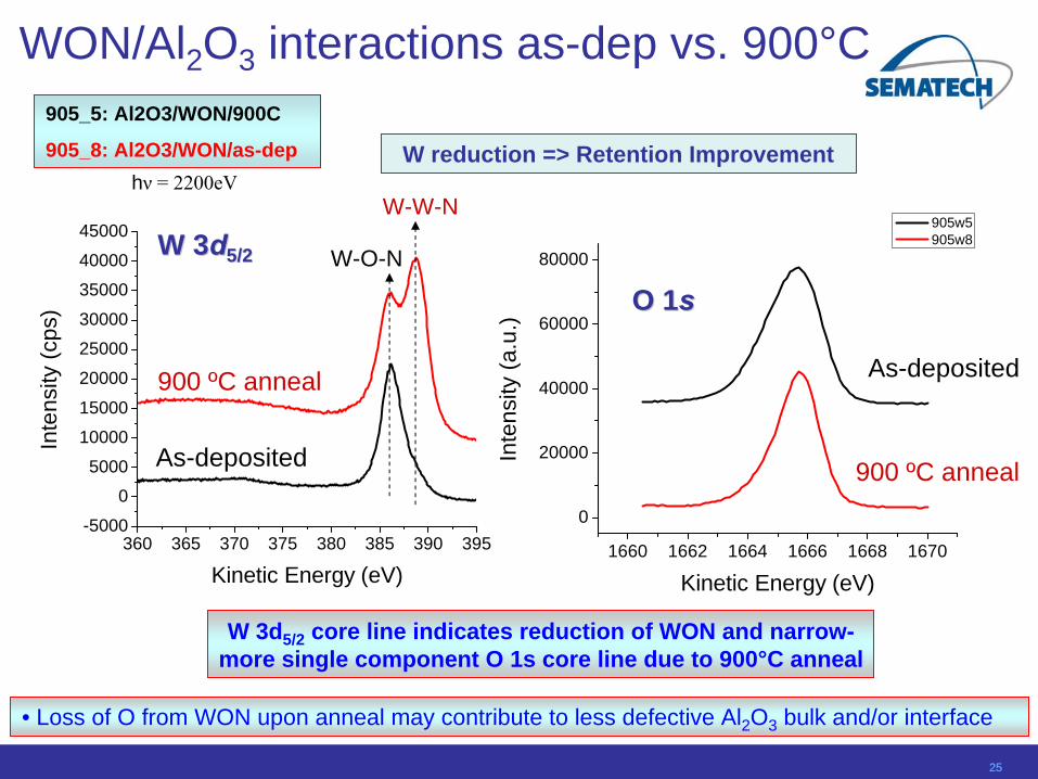
360 365 370 375 380 385 390 395-5000
0
5000
10000
15000
20000
25000
30000
35000
40000
45000
Inte
nsity
(cps
)
Kinetic Energy (eV)
W-O-N
W-W-N
W 3W 3dd5/25/2
900 ºC anneal
As-deposited
WON/Al2 O3 interactions as-dep vs. 900°C
W reduction => Retention Improvement
• Loss of O from WON upon anneal may contribute to less defective Al2 O3 bulk and/or interface
1660 1662 1664 1666 1668 1670
0
20000
40000
60000
80000
Inte
nsity
(a.u
.)
Kinetic Energy (eV)
905w5 905w8
O 1O 1ss
905_5: Al2O3/WON/900C
905_8: Al2O3/WON/as-dep
900 ºC anneal
As-deposited
W 3d5/2 core line indicates reduction of WON and narrow- more single component O 1s core line due to 900°C anneal
hν
= 2200eV
26
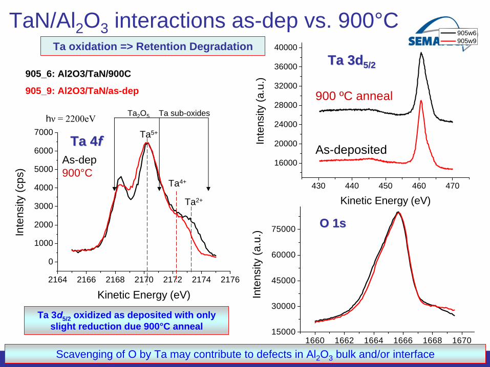
905_6: Al2O3/TaN/900C
905_9: Al2O3/TaN/as-dep
430 440 450 460 470
16000
20000
24000
28000
32000
36000
40000
Inte
nsity
(a.u
.)
Kinetic Energy (eV)
905w6 905w9
Ta 3d5/2 oxidized as deposited with only slight reduction due 900°C anneal
2164 2166 2168 2170 2172 2174 2176
0
1000
2000
3000
4000
5000
6000
7000
Inte
nsity
(cps
)
Kinetic Energy (eV)
Ta4+
Ta2+
Ta5+
Ta 4Ta 4ffAs-dep 900°C
Ta2 O5 Ta sub-oxides
Ta oxidation => Retention DegradationTa 3dTa 3d5/25/2
1660 1662 1664 1666 1668 167015000
30000
45000
60000
75000
Inte
nsity
(a.u
.)
Kinetic Energy (eV)
O 1sO 1s
Scavenging of O by Ta may contribute to defects in Al2 O3 bulk and/or interface
TaN/Al2 O3 interactions as-dep vs. 900°C
As-deposited
900 ºC anneal
hν
= 2200eV
272728 August 2009 27
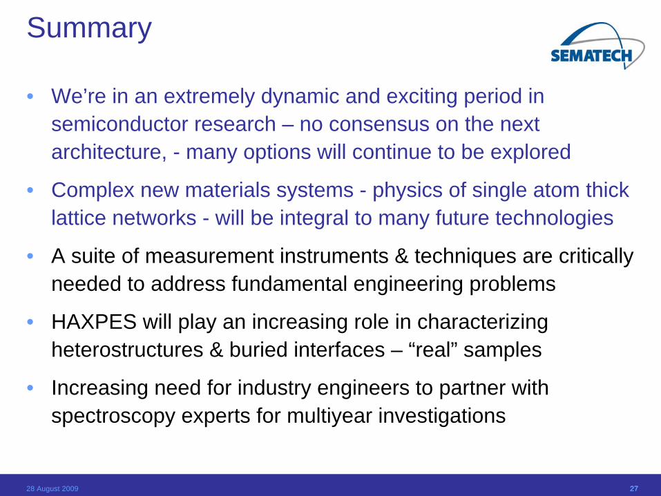
Summary
• We’re in an extremely dynamic and exciting period in semiconductor research – no consensus on the next architecture, - many options will continue to be explored
• Complex new materials systems - physics of single atom thick lattice networks - will be integral to many future technologies
• A suite of measurement instruments & techniques are critically needed to address fundamental engineering problems
• HAXPES will play an increasing role in characterizing heterostructures & buried interfaces – “real” samples
• Increasing need for industry engineers to partner with spectroscopy experts for multiyear investigations
28
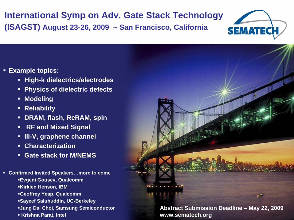
Example topics: High-k dielectrics/electrodes Physics of dielectric defects Modeling Reliability DRAM, flash, ReRAM, spin RF and Mixed Signal III-V, graphene channel Characterization Gate stack for M/NEMS
Confirmed Invited Speakers…more to comeEvgeni Gousev, QualcommKirklen Henson, IBMGeoffrey Yeap, QualcommSayeef Saluhuddin, UC-BerkeleyJung Dal Choi, Samsung Semiconductor Krishna Parat, Intel
International Symp on Adv. Gate Stack Technology (ISAGST) August 23-26, 2009 ~ San Francisco, California
Abstract Submission Deadline – May 22, 2009 www.sematech.org
29
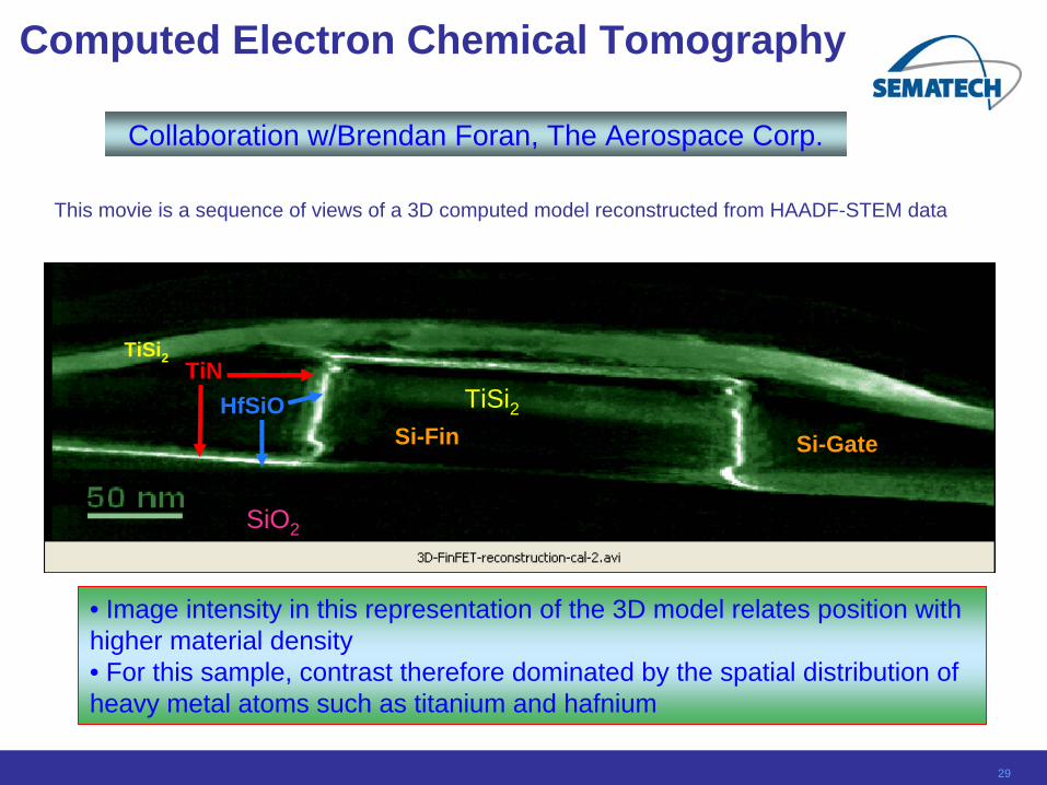
Computed Electron Chemical Tomography
This movie is a sequence of views of a 3D computed model reconstructed from HAADF-STEM data
TiSi2Si-Fin
SiO2
Si-Gate
TiSi2TiN
HfSiO
• Image intensity in this representation of the 3D model relates position with higher material density • For this sample, contrast therefore dominated by the spatial distribution of heavy metal atoms such as titanium and hafnium
Collaboration w/Brendan Foran, The Aerospace Corp.