Embed Size (px)
Citation preview
Intermediate Frequency Transmitter, 800 MHz to 4000 MHz
Data Sheet HMC8200LP5ME
Rev. B Document Feedback Information furnished by Analog Devices is believed to be accurate and reliable. However, no responsibility is assumed by Analog Devices for its use, nor for any infringements of patents or other rights of third parties that may result from its use. Specifications subject to change without notice. No license is granted by implication or otherwise under any patent or patent rights of Analog Devices. Trademarks and registered trademarks are the property of their respective owners.
One Technology Way, P.O. Box 9106, Norwood, MA 02062-9106, U.S.A. Tel: 781.329.4700 ©2016 Analog Devices, Inc. All rights reserved. Technical Support www.analog.com
FEATURES High linearity: supports modulations to 1024 QAM Tx IF range: 200 MHz to 700 MHz Tx RF range: 800 MHz to 4000 MHz Tx power control: 25 dB SPI controlled interface 32-lead, 5 mm × 5 mm LFCSP package
APPLICATIONS Point to point communications Satellite communications Wireless microwave backhaul systems
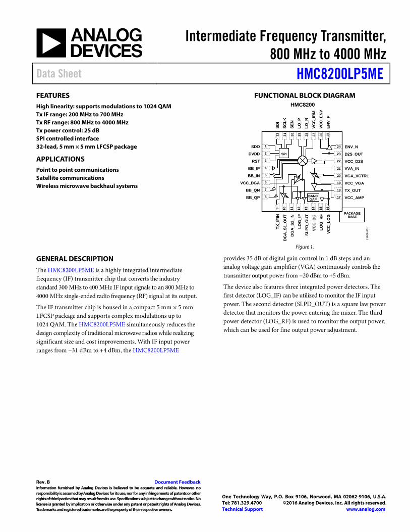
FUNCTIONAL BLOCK DIAGRAM
17
18
19
20
21
22
23
24
2526272829303132SD
I
SCLK
SEN
LO_P
LO_N
VCC
_IR
M
VCC
_EN
V
ENV_
P
ENV_N
D2S_OUT
VCC_D2S
VVA_IN
VGA_VCTRL
VCC_VGA
TX_OUT
VCC_AMP
PACKAGEBASE
TX_I
FIN
DG
A_S
1_O
UT
DG
A_S
2_IN
LOG
_IF
SLPD
_OU
T
VCC
_BG
LOG
_RF
VCC
_LO
G
SDO
DVDD
RST
BB_IP
BB_IN
VCC_DGA
BB_QN
BB_QP
1
3
4
2
5
6
7
8
9 121110 13 14 15 16
SPI
BANDGAP
1386
8-00
1
HMC8200
Figure 1.
GENERAL DESCRIPTION The HMC8200LP5ME is a highly integrated intermediate frequency (IF) transmitter chip that converts the industry standard 300 MHz to 400 MHz IF input signals to an 800 MHz to 4000 MHz single-ended radio frequency (RF) signal at its output.
The IF transmitter chip is housed in a compact 5 mm × 5 mm LFCSP package and supports complex modulations up to 1024 QAM. The HMC8200LP5ME simultaneously reduces the design complexity of traditional microwave radios while realizing significant size and cost improvements. With IF input power ranges from −31 dBm to +4 dBm, the HMC8200LP5ME
provides 35 dB of digital gain control in 1 dB steps and an analog voltage gain amplifier (VGA) continuously controls the transmitter output power from −20 dBm to +5 dBm.
The device also features three integrated power detectors. The first detector (LOG_IF) can be utilized to monitor the IF input power. The second detector (SLPD_OUT) is a square law power detector that monitors the power entering the mixer. The third power detector (LOG_RF) is used to monitor the output power, which can be used for fine output power adjustment.
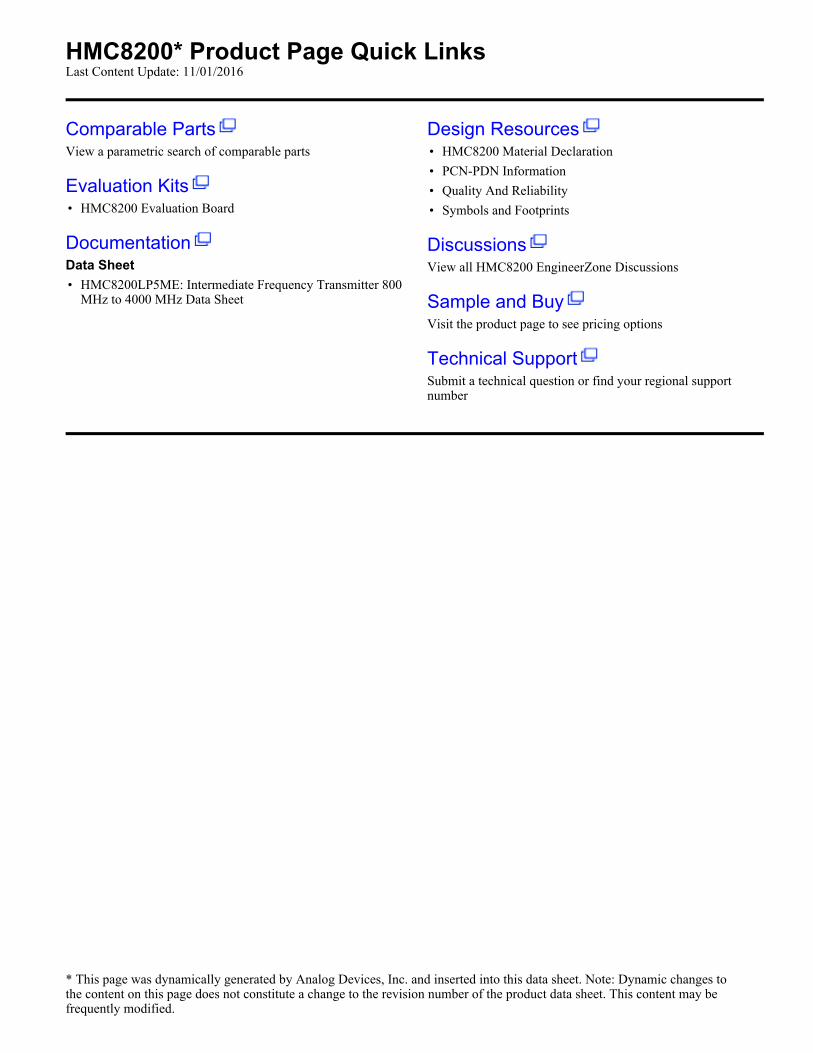
HMC8200* Product Page Quick LinksLast Content Update: 11/01/2016
Comparable PartsView a parametric search of comparable parts
Evaluation Kits• HMC8200 Evaluation Board
DocumentationData Sheet• HMC8200LP5ME: Intermediate Frequency Transmitter 800
MHz to 4000 MHz Data Sheet
Design Resources• HMC8200 Material Declaration• PCN-PDN Information• Quality And Reliability• Symbols and Footprints
DiscussionsView all HMC8200 EngineerZone Discussions
Sample and BuyVisit the product page to see pricing options
Technical SupportSubmit a technical question or find your regional support number
* This page was dynamically generated by Analog Devices, Inc. and inserted into this data sheet. Note: Dynamic changes to the content on this page does not constitute a change to the revision number of the product data sheet. This content may be frequently modified.

HMC8200LP5ME Data Sheet
Rev. B | Page 2 of 25
TABLE OF CONTENTS Features .............................................................................................. 1 Applications ....................................................................................... 1 Functional Block Diagram .............................................................. 1 General Description ......................................................................... 1 Revision History ............................................................................... 2 Specifications ..................................................................................... 3
Electrical Characteristics: 800 MHz to 1800 MHz RF Frequency Range .......................................................................... 3 Electrical Characteristics: 1800 MHz to 2800 MHz RF Frequency Range .......................................................................... 4 Electrical Characteristics: 2800 MHz to 4000 MHz RF Frequency Range .......................................................................... 5
Absolute Maximum Ratings ............................................................ 6
ESD Caution...................................................................................6 Pin Configuration and Function Descriptions ..............................7 Typical Performance Characteristics ..............................................8 Theory of Operation ...................................................................... 18
Register Array Assignments and Serial Interface ................... 18 Register Descriptions ..................................................................... 20
Register Array Assignments ...................................................... 20 Evaluation Printed Circuit Board (PCB) ..................................... 23
Evaluation PCB Schematic ........................................................ 24 Outline Dimensions ....................................................................... 25
Ordering Guide .......................................................................... 25
REVISION HISTORY 6/2016—v01.0216 to Rev. B
This Hittite Microwave Products data sheet has been reformatted to meet the styles and standards of Analog Devices, Inc.
Updated Format .................................................................. Universal Added Pin Configuration Diagram, Renumbered Sequentially ....................................................................................... 7 Added Ordering Guide .................................................................. 22 Change to y-Axis Label, Figure 42 ................................................ 14
Data Sheet HMC8200LP5ME
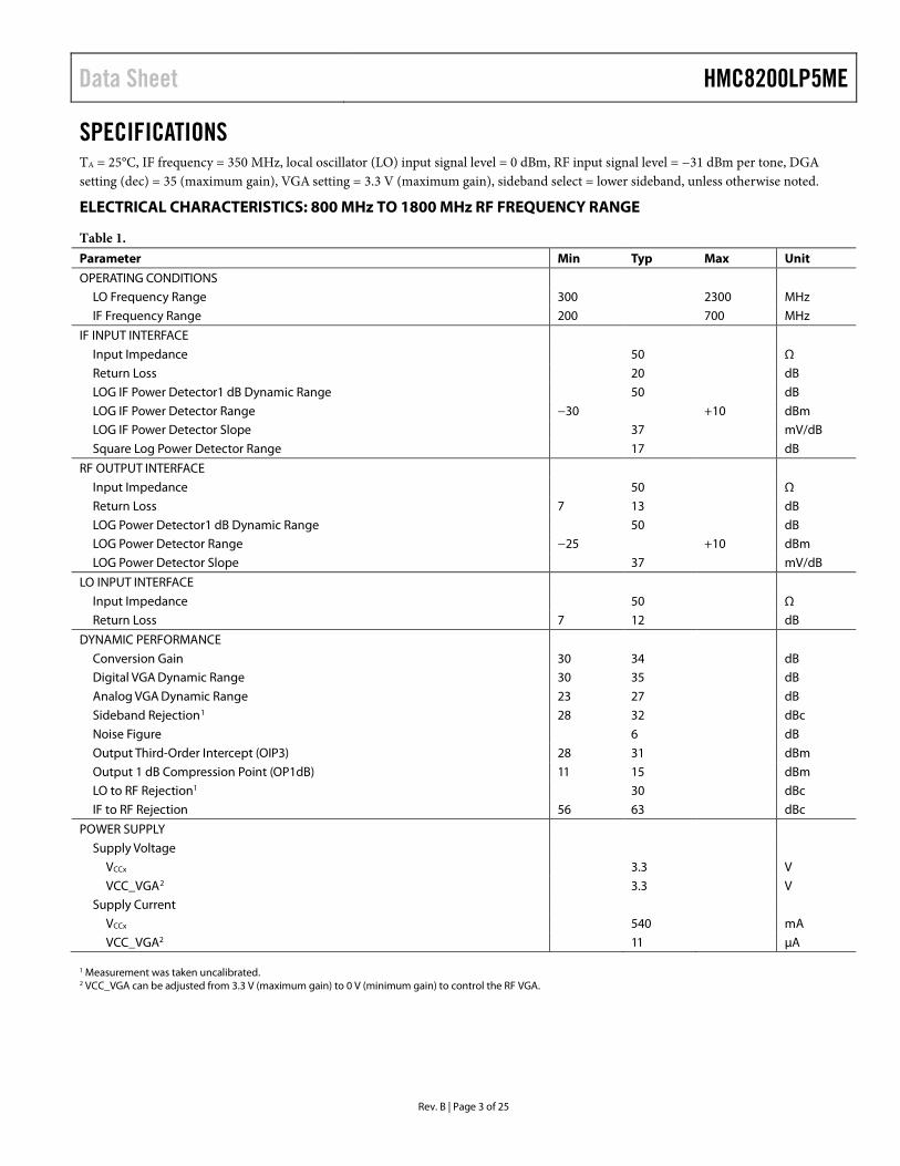
Rev. B | Page 3 of 25
SPECIFICATIONS TA = 25°C, IF frequency = 350 MHz, local oscillator (LO) input signal level = 0 dBm, RF input signal level = −31 dBm per tone, DGA setting (dec) = 35 (maximum gain), VGA setting = 3.3 V (maximum gain), sideband select = lower sideband, unless otherwise noted.
ELECTRICAL CHARACTERISTICS: 800 MHz TO 1800 MHz RF FREQUENCY RANGE
Table 1. Parameter Min Typ Max Unit OPERATING CONDITIONS
LO Frequency Range 300 2300 MHz IF Frequency Range 200 700 MHz
IF INPUT INTERFACE Input Impedance 50 Ω Return Loss 20 dB LOG IF Power Detector1 dB Dynamic Range 50 dB LOG IF Power Detector Range −30 +10 dBm LOG IF Power Detector Slope 37 mV/dB Square Log Power Detector Range 17 dB
RF OUTPUT INTERFACE Input Impedance 50 Ω Return Loss 7 13 dB LOG Power Detector1 dB Dynamic Range 50 dB LOG Power Detector Range −25 +10 dBm LOG Power Detector Slope 37 mV/dB
LO INPUT INTERFACE Input Impedance 50 Ω Return Loss 7 12 dB
DYNAMIC PERFORMANCE Conversion Gain 30 34 dB Digital VGA Dynamic Range 30 35 dB Analog VGA Dynamic Range 23 27 dB Sideband Rejection1 28 32 dBc Noise Figure 6 dB Output Third-Order Intercept (OIP3) 28 31 dBm Output 1 dB Compression Point (OP1dB) 11 15 dBm LO to RF Rejection1 30 dBc IF to RF Rejection 56 63 dBc
POWER SUPPLY Supply Voltage
VCCx 3.3 V VCC_VGA2 3.3 V
Supply Current VCCx 540 mA VCC_VGA2 11 μA
1 Measurement was taken uncalibrated. 2 VCC_VGA can be adjusted from 3.3 V (maximum gain) to 0 V (minimum gain) to control the RF VGA.
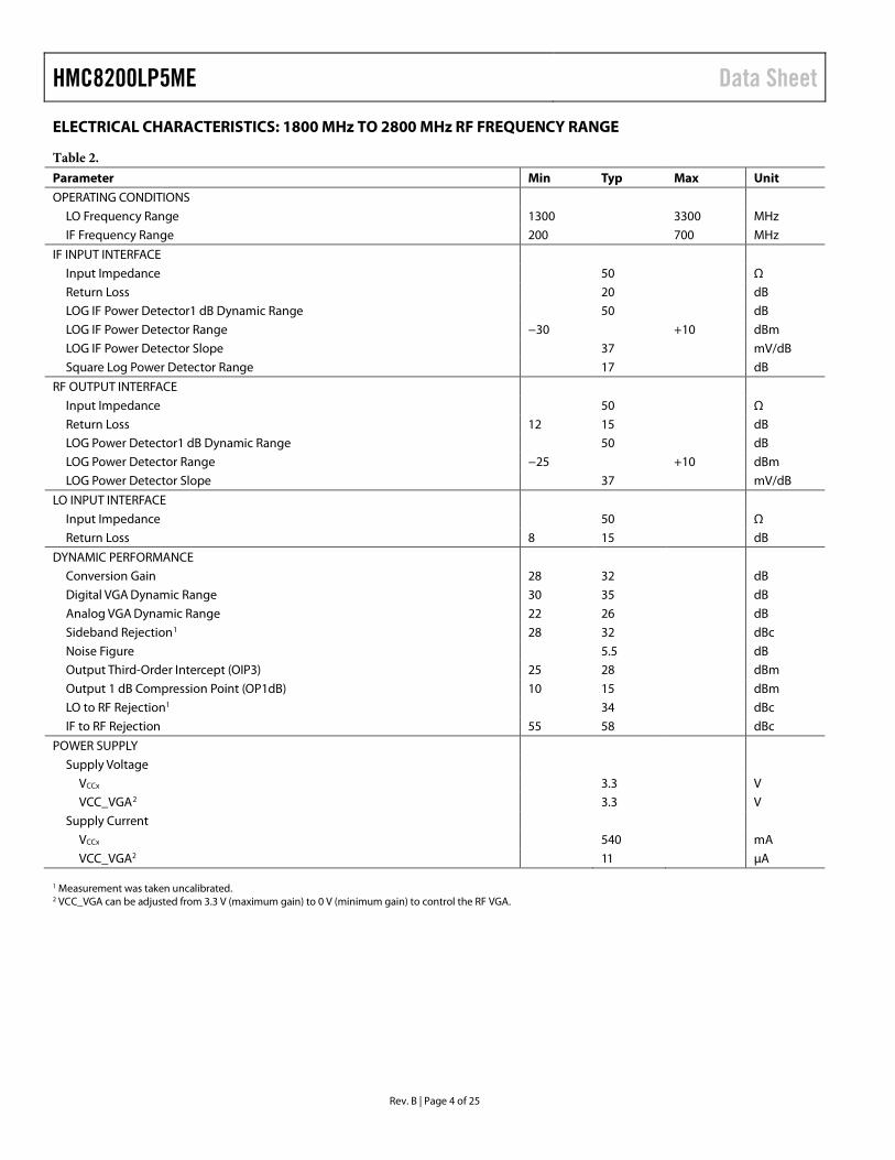
HMC8200LP5ME Data Sheet
Rev. B | Page 4 of 25
ELECTRICAL CHARACTERISTICS: 1800 MHz TO 2800 MHz RF FREQUENCY RANGE
Table 2. Parameter Min Typ Max Unit OPERATING CONDITIONS
LO Frequency Range 1300 3300 MHz IF Frequency Range 200 700 MHz
IF INPUT INTERFACE Input Impedance 50 Ω Return Loss 20 dB LOG IF Power Detector1 dB Dynamic Range 50 dB LOG IF Power Detector Range −30 +10 dBm LOG IF Power Detector Slope 37 mV/dB Square Log Power Detector Range 17 dB
RF OUTPUT INTERFACE Input Impedance 50 Ω Return Loss 12 15 dB LOG Power Detector1 dB Dynamic Range 50 dB LOG Power Detector Range −25 +10 dBm LOG Power Detector Slope 37 mV/dB
LO INPUT INTERFACE Input Impedance 50 Ω Return Loss 8 15 dB
DYNAMIC PERFORMANCE Conversion Gain 28 32 dB Digital VGA Dynamic Range 30 35 dB Analog VGA Dynamic Range 22 26 dB Sideband Rejection1 28 32 dBc Noise Figure 5.5 dB Output Third-Order Intercept (OIP3) 25 28 dBm Output 1 dB Compression Point (OP1dB) 10 15 dBm LO to RF Rejection1 34 dBc IF to RF Rejection 55 58 dBc
POWER SUPPLY Supply Voltage
VCCx 3.3 V VCC_VGA2 3.3 V
Supply Current VCCx 540 mA VCC_VGA2 11 μA
1 Measurement was taken uncalibrated. 2 VCC_VGA can be adjusted from 3.3 V (maximum gain) to 0 V (minimum gain) to control the RF VGA.
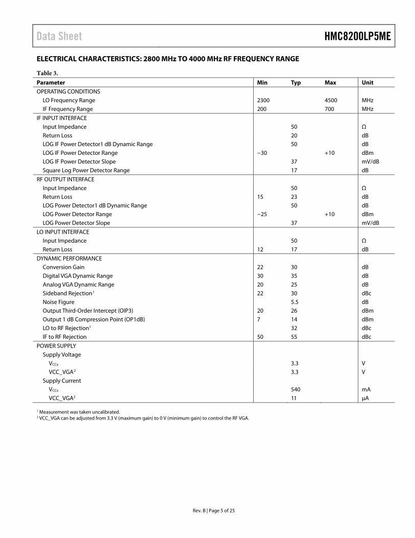
Data Sheet HMC8200LP5ME
Rev. B | Page 5 of 25
ELECTRICAL CHARACTERISTICS: 2800 MHz TO 4000 MHz RF FREQUENCY RANGE
Table 3. Parameter Min Typ Max Unit OPERATING CONDITIONS
LO Frequency Range 2300 4500 MHz IF Frequency Range 200 700 MHz
IF INPUT INTERFACE Input Impedance 50 Ω Return Loss 20 dB LOG IF Power Detector1 dB Dynamic Range 50 dB LOG IF Power Detector Range −30 +10 dBm LOG IF Power Detector Slope 37 mV/dB Square Log Power Detector Range 17 dB
RF OUTPUT INTERFACE Input Impedance 50 Ω Return Loss 15 23 dB LOG Power Detector1 dB Dynamic Range 50 dB LOG Power Detector Range −25 +10 dBm LOG Power Detector Slope 37 mV/dB
LO INPUT INTERFACE Input Impedance 50 Ω Return Loss 12 17 dB
DYNAMIC PERFORMANCE Conversion Gain 22 30 dB Digital VGA Dynamic Range 30 35 dB Analog VGA Dynamic Range 20 25 dB Sideband Rejection1 22 30 dBc Noise Figure 5.5 dB Output Third-Order Intercept (OIP3) 20 26 dBm Output 1 dB Compression Point (OP1dB) 7 14 dBm LO to RF Rejection1 32 dBc IF to RF Rejection 50 55 dBc
POWER SUPPLY Supply Voltage
VCCx 3.3 V VCC_VGA2 3.3 V
Supply Current VCCx 540 mA VCC_VGA2 11 μA
1 Measurement was taken uncalibrated. 2 VCC_VGA can be adjusted from 3.3 V (maximum gain) to 0 V (minimum gain) to control the RF VGA.
HMC8200LP5ME Data Sheet
Rev. B | Page 6 of 25
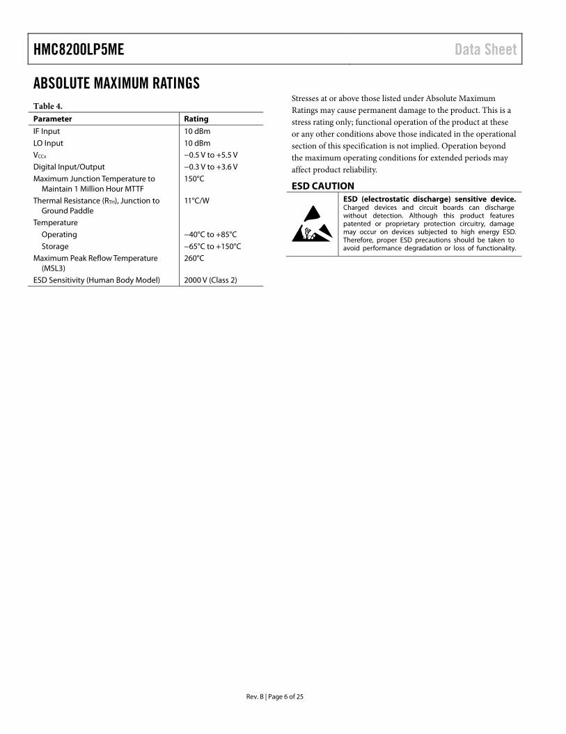
ABSOLUTE MAXIMUM RATINGS Table 4. Parameter Rating IF Input 10 dBm LO Input 10 dBm VCCx −0.5 V to +5.5 V Digital Input/Output −0.3 V to +3.6 V Maximum Junction Temperature to
Maintain 1 Million Hour MTTF 150°C
Thermal Resistance (RTH), Junction to Ground Paddle
11°C/W
Temperature Operating −40°C to +85°C Storage −65°C to +150°C
Maximum Peak Reflow Temperature (MSL3)
260°C
ESD Sensitivity (Human Body Model) 2000 V (Class 2)
Stresses at or above those listed under Absolute Maximum Ratings may cause permanent damage to the product. This is a stress rating only; functional operation of the product at these or any other conditions above those indicated in the operational section of this specification is not implied. Operation beyond the maximum operating conditions for extended periods may affect product reliability.
ESD CAUTION
Data Sheet HMC8200LP5ME
Rev. B | Page 7 of 25
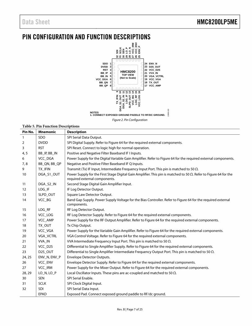
PIN CONFIGURATION AND FUNCTION DESCRIPTIONS
1386
8-10
0
24 ENV_N23 D2S_OUT22 VCC_D2S21 VVA_IN20 VGA_VCTRL19 VCC_VGA18 TX_OUT17 VCC_AMP
12345678
SDODVDD
RSTBB_IPBB_IN
VCC_DGABB_QNBB_QP
9 10 11 12 13 14 15 16
TX_I
FIN
DG
A_S
1_O
UT
DG
A_S
2_IN
LOG
_IF
SLPD
_OU
TVC
C_B
GLO
G_R
FVC
C_L
OG
32 31 30 29 28 27 26 25
SDI
SCLK
SEN
LO_P
LO_N
VCC
_IR
MVC
C_E
NV
ENV_
P
HMC8200TOP VIEW
(Not to Scale)
NOTES1. CONNECT EXPOSED GROUND PADDLE TO RF/DC GROUND.
Figure 2. Pin Configuration
Table 5. Pin Function Descriptions Pin No. Mnemonic Description 1 SDO SPI Serial Data Output. 2 DVDD SPI Digital Supply. Refer to Figure 64 for the required external components. 3 RST SPI Reset. Connect to logic high for normal operation. 4, 5 BB_IP, BB_IN Positive and Negative Filter Baseband IF I Inputs. 6 VCC_DGA Power Supply for the Digital Variable Gain Amplifier. Refer to Figure 64 for the required external components. 7, 8 BB_QN, BB_QP Negative and Positive Filter Baseband IF Q Inputs. 9 TX_IFIN Transmit (Tx) IF Input, Intermediate Frequency Input Port. This pin is matched to 50 Ω. 10 DGA_S1_OUT Power Supply for the First Stage Digital Gain Amplifier. This pin is matched to 50 Ω. Refer to Figure 64 for the
required external components. 11 DGA_S2_IN Second Stage Digital Gain Amplifier Input. 12 LOG_IF IF Log Detector Output. 13 SLPD_OUT Square Law Detector Output. 14 VCC_BG Band Gap Supply. Power Supply Voltage for the Bias Controller. Refer to Figure 64 for the required external
components. 15 LOG_RF RF Log Detector Output. 16 VCC_LOG RF Log Detector Supply. Refer to Figure 64 for the required external components. 17 VCC_AMP Power Supply for the RF Output Amplifier. Refer to Figure 64 for the required external components. 18 TX_OUT Tx Chip Output. 19 VCC_VGA Power Supply for the Variable Gain Amplifier. Refer to Figure 64 for the required external components. 20 VGA_VCTRL VGA Control Voltage. Refer to Figure 64 for the required external components. 21 VVA_IN VVA Intermediate Frequency Input Port. This pin is matched to 50 Ω. 22 VCC_D2S Differential to Single Amplifier Supply. Refer to Figure 64 for the required external components. 23 D2S_OUT Differential to Single Amplifier Intermediate Frequency Output Port. This pin is matched to 50 Ω. 24, 25 ENV_N, ENV_P Envelope Detector Outputs. 26 VCC_ENV Envelope Detector Supply. Refer to Figure 64 for the required external components. 27 VCC_IRM Power Supply for the Mixer Output. Refer to Figure 64 for the required external components. 28, 29 LO_N, LO_P Local Oscillator Inputs. These pins are ac-coupled and matched to 50 Ω. 30 SEN SPI Serial Enable. 31 SCLK SPI Clock Digital Input. 32 SDI SPI Serial Data Input. EPAD Exposed Pad. Connect exposed ground paddle to RF/dc ground.
HMC8200LP5ME Data Sheet
Rev. B | Page 8 of 25
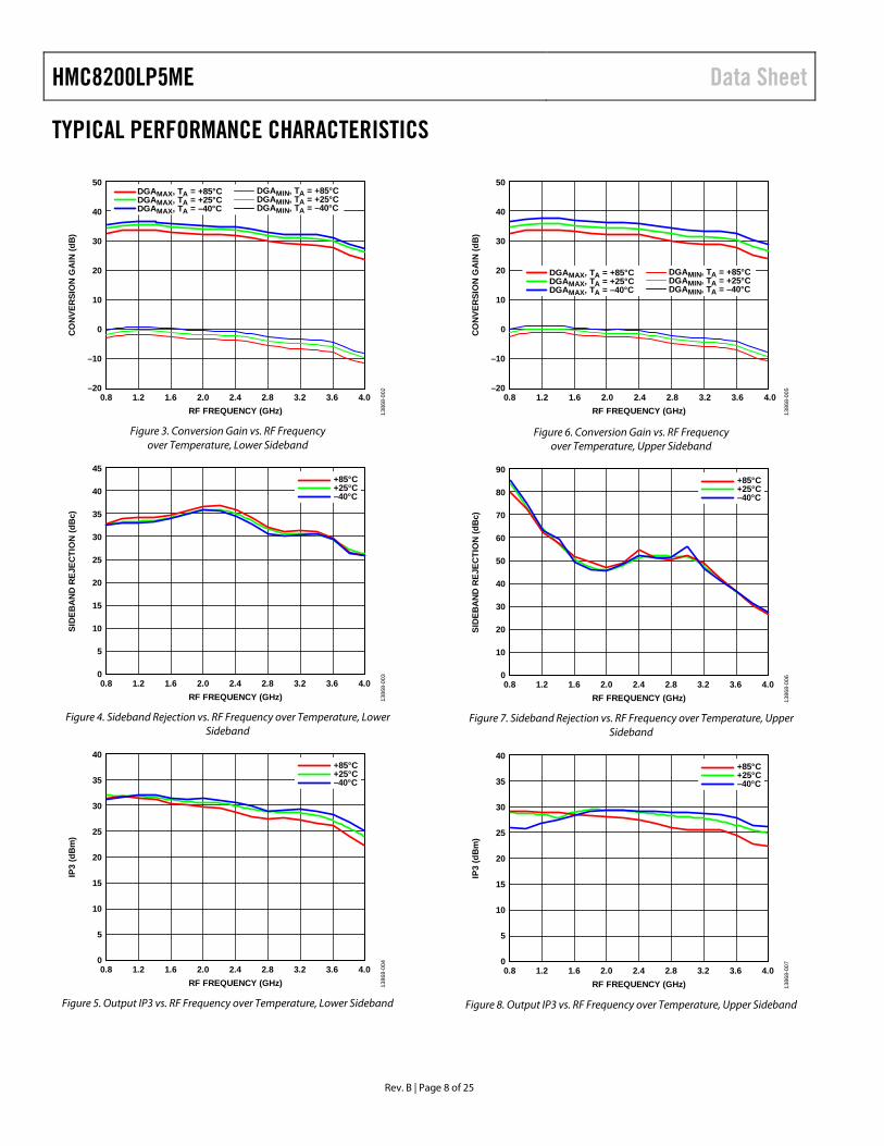
TYPICAL PERFORMANCE CHARACTERISTICS
50
–200.8 1.61.2 2.0 2.4 2.8 3.2 3.6 4.0
CO
NVE
RSI
ON
GA
IN (d
B)
RF FREQUENCY (GHz)
–10
0
10
20
30
40
DGAMAX, TA = +85°CDGAMAX, TA = +25°CDGAMAX, TA = –40°C
DGAMIN, TA = +85°CDGAMIN, TA = +25°CDGAMIN, TA = –40°C
1386
8-00
2
Figure 3. Conversion Gain vs. RF Frequency
over Temperature, Lower Sideband
45
0
SID
EBA
ND
REJ
ECTI
ON
(dB
c)
5
10
15
20
25
30
35
40
0.8 1.61.2 2.0 2.4 2.8 3.2 3.6 4.0RF FREQUENCY (GHz)
+85°C+25°C–40°C
1386
8-00
3
Figure 4. Sideband Rejection vs. RF Frequency over Temperature, Lower
Sideband
40
0
IP3
(dB
m)
5
10
15
20
25
30
35
0.8 1.61.2 2.0 2.4 2.8 3.2 3.6 4.0RF FREQUENCY (GHz)
+85°C+25°C–40°C
1386
8-00
4
Figure 5. Output IP3 vs. RF Frequency over Temperature, Lower Sideband
50
–200.8 1.61.2 2.0 2.4 2.8 3.2 3.6 4.0
CO
NVE
RSI
ON
GA
IN (d
B)
RF FREQUENCY (GHz)
–10
0
10
20
30
40
1386
8-00
5
DGAMAX, TA = +85°CDGAMAX, TA = +25°CDGAMAX, TA = –40°C
DGAMIN, TA = +85°CDGAMIN, TA = +25°CDGAMIN, TA = –40°C
Figure 6. Conversion Gain vs. RF Frequency
over Temperature, Upper Sideband
90
0
SID
EBA
ND
REJ
ECTI
ON
(dB
c)
0.8 1.61.2 2.0 2.4 2.8 3.2 3.6 4.0RF FREQUENCY (GHz)
+85°C+25°C–40°C
10
20
30
40
50
60
70
80
1386
8-00
6
Figure 7. Sideband Rejection vs. RF Frequency over Temperature, Upper
Sideband
40
0
IP3
(dB
m)
0.8 1.61.2 2.0 2.4 2.8 3.2 3.6 4.0RF FREQUENCY (GHz)
+85°C+25°C–40°C
5
10
15
20
25
30
3513
868-
007
Figure 8. Output IP3 vs. RF Frequency over Temperature, Upper Sideband
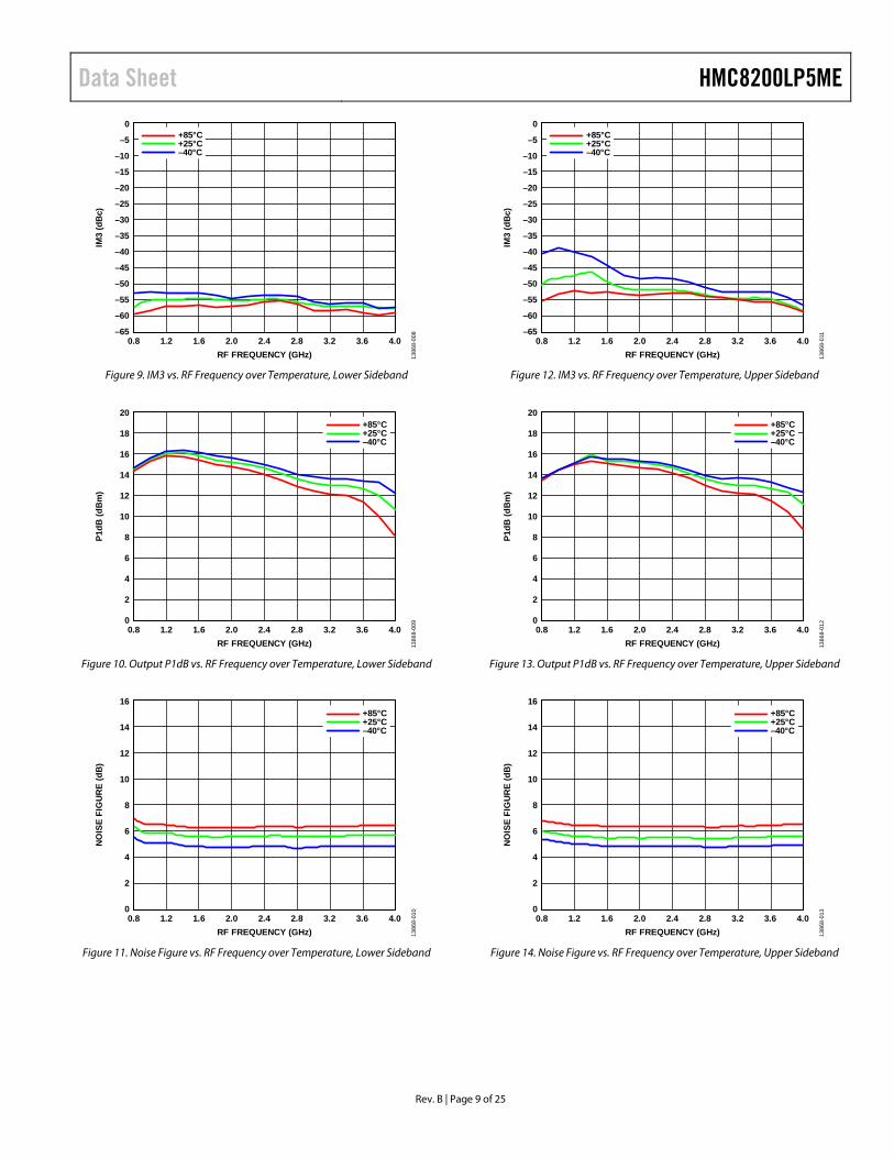
Data Sheet HMC8200LP5ME
Rev. B | Page 9 of 25
0
–65
IM3
(dB
c)
–60
–55
–50
–45
–40
–35
–30
–25
–20
–15
–10
–5
0.8 1.61.2 2.0 2.4 2.8 3.2 3.6 4.0RF FREQUENCY (GHz)
+85°C+25°C–40°C
1386
8-00
8
Figure 9. IM3 vs. RF Frequency over Temperature, Lower Sideband
20
0
P1dB
(dB
m)
2
4
6
8
10
12
14
16
18
0.8 1.61.2 2.0 2.4 2.8 3.2 3.6 4.0RF FREQUENCY (GHz)
+85°C+25°C–40°C
1386
8-00
9
Figure 10. Output P1dB vs. RF Frequency over Temperature, Lower Sideband
16
0
4
10
14
8
2
6
12
NO
ISE
FIG
UR
E (d
B)
0.8 1.61.2 2.0 2.4 2.8 3.2 3.6 4.0RF FREQUENCY (GHz)
+85°C+25°C–40°C
1386
8-01
0
Figure 11. Noise Figure vs. RF Frequency over Temperature, Lower Sideband
0
–65
IM3
(dB
c)
–60
–55
–50
–45
–40
–35
–30
–25
–20
–15
–10
–5
0.8 1.61.2 2.0 2.4 2.8 3.2 3.6 4.0RF FREQUENCY (GHz)
+85°C+25°C–40°C
1386
8-01
1
Figure 12. IM3 vs. RF Frequency over Temperature, Upper Sideband
20
0
P1dB
(dB
m)
2
4
6
8
10
12
14
16
18
0.8 1.61.2 2.0 2.4 2.8 3.2 3.6 4.0RF FREQUENCY (GHz)
+85°C+25°C–40°C
1386
8-01
2
Figure 13. Output P1dB vs. RF Frequency over Temperature, Upper Sideband
16
0
4
10
14
8
2
6
12
NO
ISE
FIG
UR
E (d
B)
0.8 1.61.2 2.0 2.4 2.8 3.2 3.6 4.0RF FREQUENCY (GHz)
+85°C+25°C–40°C
1386
8-01
3
Figure 14. Noise Figure vs. RF Frequency over Temperature, Upper Sideband
HMC8200LP5ME Data Sheet
Rev. B | Page 10 of 25
45
0
CO
NVE
RSI
ON
GA
IN (d
B)
5
10
15
20
25
30
35
40
0.8 1.61.2 2.0 2.4 2.8 3.2 3.6 4.0RF FREQUENCY (GHz)
–4dBm–2dBm0dBm+2dBm+4dBm
1386
8-01
4
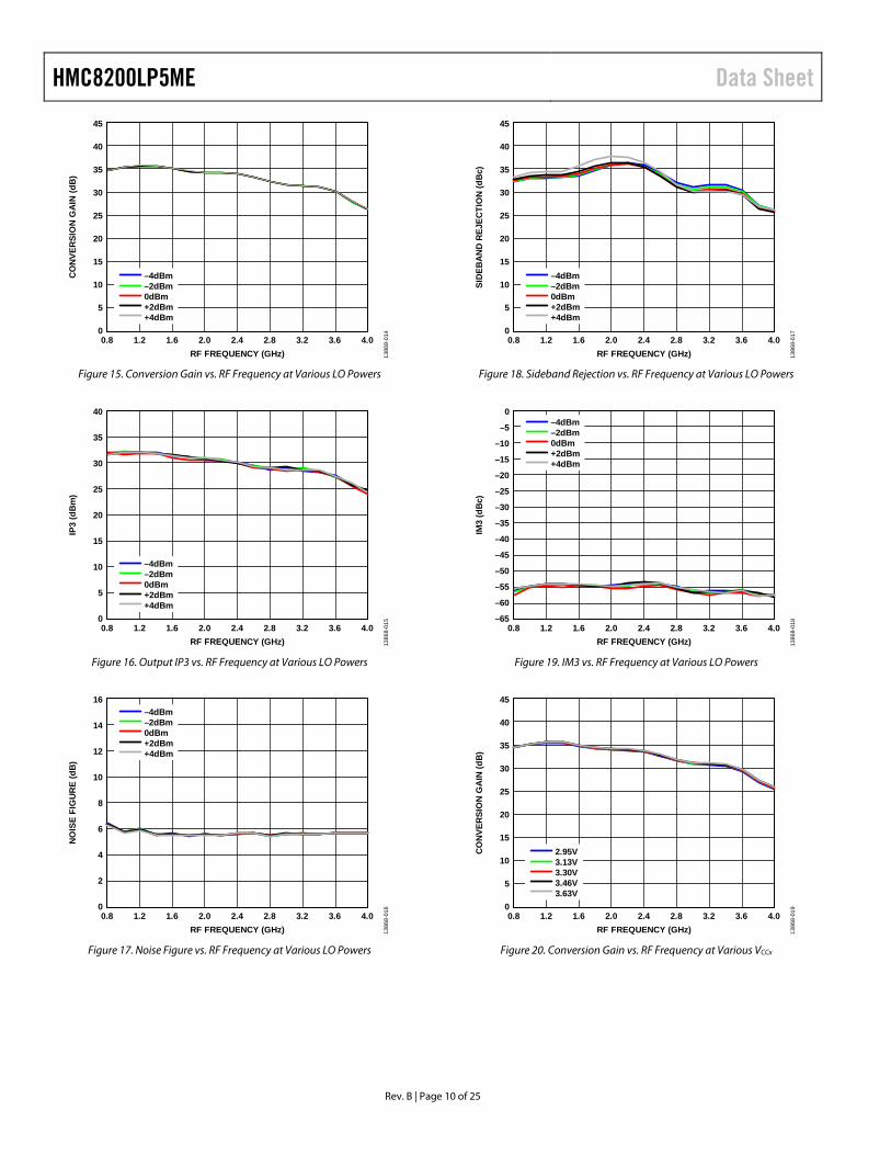
Figure 15. Conversion Gain vs. RF Frequency at Various LO Powers
40
0
IP3
(dB
m)
0.8 1.61.2 2.0 2.4 2.8 3.2 3.6 4.0RF FREQUENCY (GHz)
5
10
15
20
25
30
35
–4dBm–2dBm0dBm+2dBm+4dBm
1386
8-01
5
Figure 16. Output IP3 vs. RF Frequency at Various LO Powers
16
0
4
10
14
8
2
6
12
NO
ISE
FIG
UR
E (d
B)
0.8 1.61.2 2.0 2.4 2.8 3.2 3.6 4.0RF FREQUENCY (GHz)
–4dBm–2dBm0dBm+2dBm+4dBm
1386
8-01
6
Figure 17. Noise Figure vs. RF Frequency at Various LO Powers
45
0
SID
EBA
ND
REJ
ECTI
ON
(dB
c)
5
10
15
20
25
30
35
40
0.8 1.61.2 2.0 2.4 2.8 3.2 3.6 4.0RF FREQUENCY (GHz)
–4dBm–2dBm0dBm+2dBm+4dBm
1386
8-01
7
Figure 18. Sideband Rejection vs. RF Frequency at Various LO Powers
0
–65
IM3
(dB
c)
–60
–55
–50
–45
–40
–35
–30
–25
–20
–15
–10
–5
0.8 1.61.2 2.0 2.4 2.8 3.2 3.6 4.0RF FREQUENCY (GHz)
–4dBm–2dBm0dBm+2dBm+4dBm
1386
8-01
8
Figure 19. IM3 vs. RF Frequency at Various LO Powers
45
0
CO
NVE
RSI
ON
GA
IN (d
B)
5
10
15
20
25
30
35
40
0.8 1.61.2 2.0 2.4 2.8 3.2 3.6 4.0RF FREQUENCY (GHz)
2.95V3.13V3.30V3.46V3.63V
1386
8-01
9
Figure 20. Conversion Gain vs. RF Frequency at Various VCCx
Data Sheet HMC8200LP5ME
Rev. B | Page 11 of 25
40
0
IP3
(dB
m)
0.8 1.61.2 2.0 2.4 2.8 3.2 3.6 4.0RF FREQUENCY (GHz)
5
10
15
20
25
30
35
2.95V3.13V3.30V3.46V3.63V
1386
8-02
0
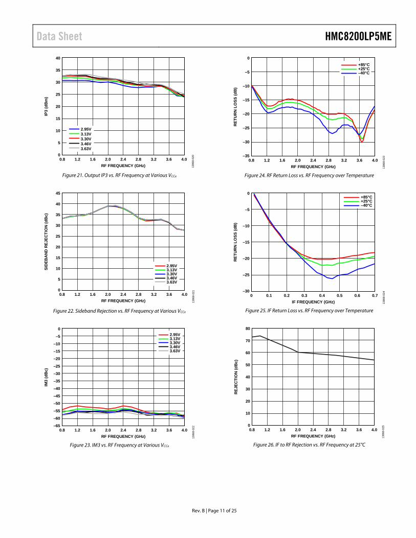
Figure 21. Output IP3 vs. RF Frequency at Various VCCx
0.8 1.2 1.6 2.0 2.4 2.8 3.2 3.6 4.0
SID
EBA
ND
REJ
ECTI
ON
(dB
c)
RF FREQUENCY (GHz)
0
5
10
15
20
25
30
35
40
45
2.95V3.13V3.30V3.46V3.63V
1386
8-02
1
Figure 22. Sideband Rejection vs. RF Frequency at Various VCCx
0.8 1.2 1.6 2.0 2.4 2.8 3.2 3.6 4.0
IM3
(dB
c)
RF FREQUENCY (GHz)
2.95V3.13V3.30V3.46V3.63V
–65
–60
–55
–50
–45
–40
–35
–30
–25
–20
–15
–10
–5
0
1386
8-02
2
Figure 23. IM3 vs. RF Frequency at Various VCCx
0.8 1.2 1.6 2.0 2.4 2.8 3.2 3.6 4.0
RET
UR
N L
OSS
(dB
)
RF FREQUENCY (GHz)
–35
–30
–25
–20
–15
–10
–5
0+85°C+25°C–40°C
1386
8-02
3
Figure 24. RF Return Loss vs. RF Frequency over Temperature
0 0.1 0.2 0.3 0.4 0.5 0.6 0.7
RET
UR
N L
OSS
(dB
)
IF FREQUENCY (GHz)
–30
–25
–20
–15
–10
–5
0+85°C+25°C–40°C
1386
8-02
4
Figure 25. IF Return Loss vs. RF Frequency over Temperature
0.8 1.2 1.6 2.0 2.4 2.8 3.2 3.6 4.0
REJ
ECTI
ON
(dB
c)
RF FREQUENCY (GHz)
0
10
20
30
40
50
60
70
80
1386
8-02
5
Figure 26. IF to RF Rejection vs. RF Frequency at 25°C
HMC8200LP5ME Data Sheet
Rev. B | Page 12 of 25
0.3 0.9 1.5 2.1 2.7 3.3 3.9 4.5
RET
UR
N L
OSS
(dB
)
LO FREQUENCY (GHz)
–25
–20
–15
–10
–5
0+85°C+25°C–40°C
1386
8-02
6
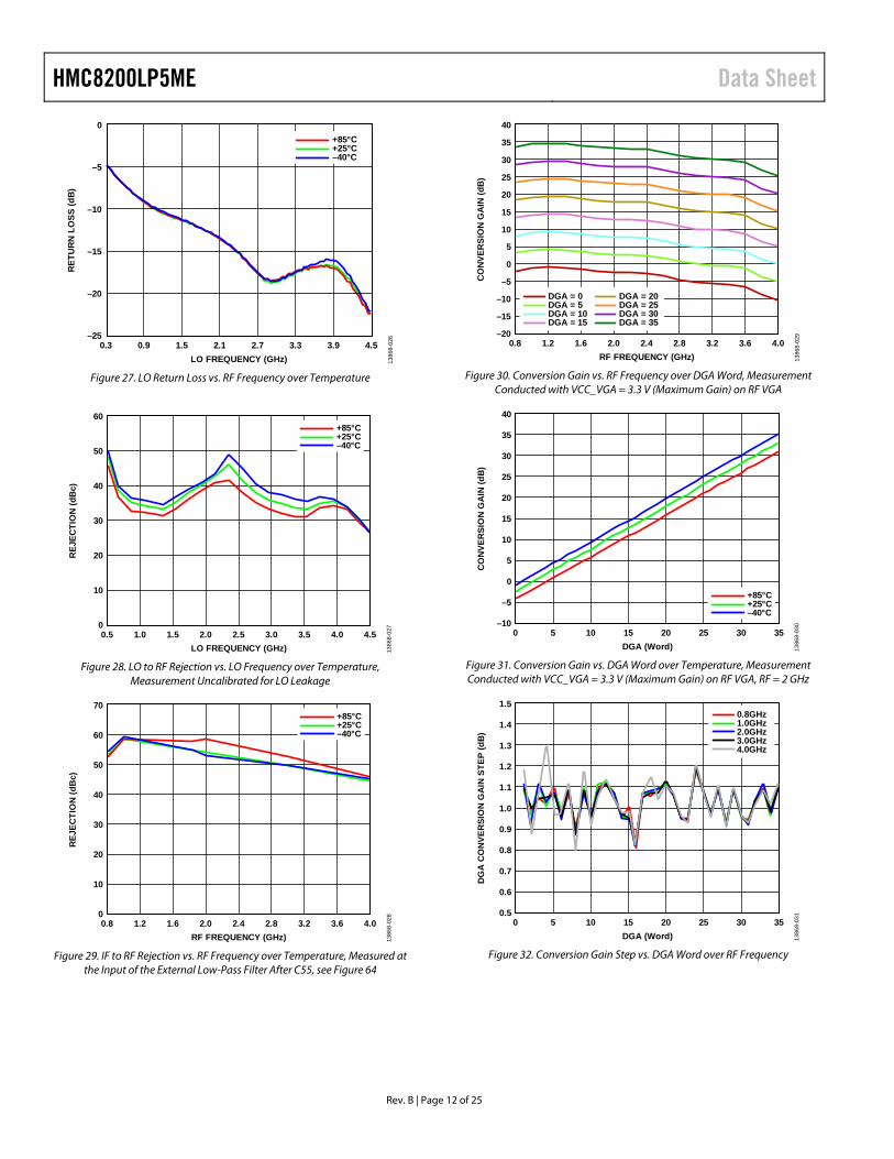
Figure 27. LO Return Loss vs. RF Frequency over Temperature
0.5 1.0 1.5 2.0 2.5 3.0 3.5 4.0 4.5
REJ
ECTI
ON
(dB
c)
LO FREQUENCY (GHz)
0
10
20
30
40
50
60+85°C+25°C–40°C
1386
8-02
7
Figure 28. LO to RF Rejection vs. LO Frequency over Temperature, Measurement Uncalibrated for LO Leakage
0.8 1.2 1.6 2.0 2.4 2.8 3.2 3.6 4.0
REJ
ECTI
ON
(dB
c)
RF FREQUENCY (GHz)
0
10
20
30
40
50
60
70+85°C+25°C–40°C
1386
8-02
8
Figure 29. IF to RF Rejection vs. RF Frequency over Temperature, Measured at the Input of the External Low-Pass Filter After C55, see Figure 64
0.8 1.2 1.6 2.0 2.4 2.8 3.2 3.6 4.0
CO
NVE
RSI
ON
GA
IN (d
B)
RF FREQUENCY (GHz)
DGA = 0DGA = 5DGA = 10DGA = 15
DGA = 20DGA = 25DGA = 30DGA = 35
–20
–15
–10
–5
0
5
10
15
20
25
30
35
40
1386
8-02
9
Figure 30. Conversion Gain vs. RF Frequency over DGA Word, Measurement Conducted with VCC_VGA = 3.3 V (Maximum Gain) on RF VGA
CO
NVE
RSI
ON
GA
IN (d
B)
–10
–5
0
5
10
15
20
25
30
35
40
+85°C+25°C–40°C
0 5 10 15 20 25 30 35DGA (Word) 13
868-
030
Figure 31. Conversion Gain vs. DGA Word over Temperature, Measurement Conducted with VCC_VGA = 3.3 V (Maximum Gain) on RF VGA, RF = 2 GHz
0 5 10 15 20 25 30 35
DG
A C
ON
VER
SIO
N G
AIN
STE
P (d
B)
DGA (Word)
0.5
0.6
0.7
0.8
0.9
1.0
1.1
1.2
1.3
1.4
1.50.8GHz1.0GHz2.0GHz3.0GHz4.0GHz
1386
8-03
1
Figure 32. Conversion Gain Step vs. DGA Word over RF Frequency
Data Sheet HMC8200LP5ME
Rev. B | Page 13 of 25
CO
NVE
RSI
ON
GA
IN (d
B)
–10
–5
0
5
10
15
20
25
30
35
40
+85°C+25°C–40°C
0 5 10 15 20 25 30 35DGA (Word) 13
868-
032
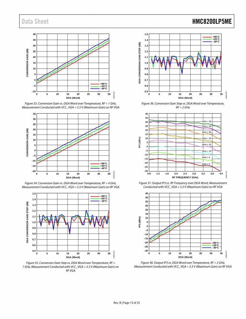
Figure 33. Conversion Gain vs. DGA Word over Temperature, RF = 1 GHz,
Measurement Conducted with VCC_VGA = 3.3 V (Maximum Gain) on RF VGA
CO
NVE
RSI
ON
GA
IN (d
B)
–20
–5
–10
–15
0
5
10
15
20
25
30
35
+85°C+25°C–40°C
0 5 10 15 20 25 30 35DGA (Word) 13
868-
033
Figure 34. Conversion Gain vs. DGA Word over Temperature, RF = 4 GHz,
Measurement Conducted with VCC_VGA = 3.3 V (Maximum Gain) on RF VGA
0 5 10 15 20 25 30 35
DG
A C
ON
VER
SIO
N G
AIN
STE
P (d
B)
DGA (Word)
0.5
0.6
0.7
0.8
0.9
1.0
1.1
1.2
1.3
1.4
1.5+85°C+25°C–40°C
1386
8-03
4
Figure 35. Conversion Gain Step vs. DGA Word over Temperature, RF =
1 GHz, Measurement Conducted with VCC_VGA = 3.3 V (Maximum Gain) on RF VGA
0 5 10 15 20 25 30 35
DG
A C
ON
VER
SIO
N G
AIN
STE
P (d
B)
DGA (Word)
0.5
0.6
0.7
0.8
0.9
1.0
1.1
1.2
1.3
1.4
1.5+85°C+25°C–40°C
1386
8-03
5
Figure 36. Conversion Gain Step vs. DGA Word over Temperature,
RF = 2 GHz
0.8 1.2 1.6 2.0 2.4 2.8 3.2 3.6 4.0
IP3
(dB
m)
RF FREQUENCY (GHz)
–30
–20–25
–15–10
–505
10152025303540
1386
8-03
6
DGA = 35
DGA = 30
DGA = 25
DGA = 20
DGA = 15
DGA = 10
DGA = 5
DGA = 0
Figure 37. Output IP3 vs. RF Frequency over DGA Word, Measurement
Conducted with VCC_VGA = 3.3 V (Maximum Gain) on RF VGA
IP3
(dB
m)
–30
–20–25
–15–10–505
10152025303540
+85°C+25°C–40°C
0 5 10 15 20 25 30 35DGA (Word) 13
868-
037
Figure 38. Output IP3 vs. DGA Word over Temperature, RF = 2 GHz,
Measurement Conducted with VCC_VGA = 3.3 V (Maximum Gain) on RF VGA
HMC8200LP5ME Data Sheet
Rev. B | Page 14 of 25
0 5 10 15 20 25 30 35
DG
A C
ON
VER
SIO
N G
AIN
STE
P (d
B)
DGA (Word)
0.5
0.6
0.7
0.8
0.9
1.0
1.1
1.2
1.3
1.4
1.5+85°C+25°C–40°C
1386
8-03
8
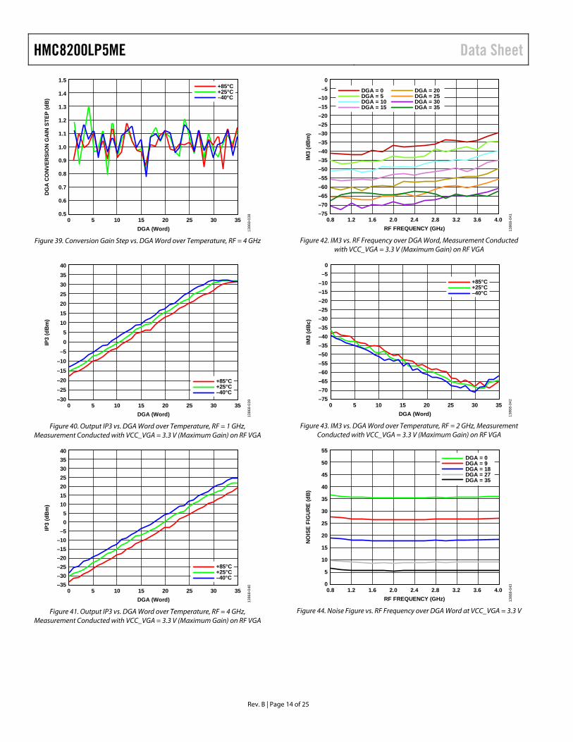
Figure 39. Conversion Gain Step vs. DGA Word over Temperature, RF = 4 GHz
IP3
(dB
m)
–30
–20–25
–15–10
–505
10152025303540
+85°C+25°C–40°C
0 5 10 15 20 25 30 35DGA (Word) 13
868-
039
Figure 40. Output IP3 vs. DGA Word over Temperature, RF = 1 GHz, Measurement Conducted with VCC_VGA = 3.3 V (Maximum Gain) on RF VGA
IP3
(dB
m)
–35–30
–20–25
–15–10
–505
10152025303540
+85°C+25°C–40°C
0 5 10 15 20 25 30 35DGA (Word) 13
868-
040
Figure 41. Output IP3 vs. DGA Word over Temperature, RF = 4 GHz, Measurement Conducted with VCC_VGA = 3.3 V (Maximum Gain) on RF VGA
0–5
–10–15–20–25–30
–40–35
–35–50–55–60
–70–65
–75
IM3
(dB
m)
RF FREQUENCY (GHz)0.8 1.2 1.6 2.4 3.22.0 2.8 3.6 4.0
DGA = 0DGA = 5DGA = 10DGA = 15
DGA = 20DGA = 25DGA = 30DGA = 35
1386
8-04
1
Figure 42. IM3 vs. RF Frequency over DGA Word, Measurement Conducted with VCC_VGA = 3.3 V (Maximum Gain) on RF VGA
0–5
–10–15–20–25–30
–40–35
–35–50–55–60
–70–65
–75
IM3
(dB
c)
DGA (Word)0 5 10 20 3015 25 35
+85°C+25°C–40°C
1386
8-04
2
Figure 43. IM3 vs. DGA Word over Temperature, RF = 2 GHz, Measurement Conducted with VCC_VGA = 3.3 V (Maximum Gain) on RF VGA
55
50
45
40
35
30
25
15
20
10
5
0
NO
ISE
FIG
UR
E (d
B)
RF FREQUENCY (GHz)0.8 1.2 1.6 2.4 3.22.0 2.8 3.6 4.0
DGA = 0DGA = 9DGA = 18DGA = 27DGA = 35
1386
8-04
3
Figure 44. Noise Figure vs. RF Frequency over DGA Word at VCC_VGA = 3.3 V
Data Sheet HMC8200LP5ME
Rev. B | Page 15 of 25
0–5
–10–15–20–25–30
–40–35
–35–50–55–60
–70–65
–75
IM3
(dB
c)
DGA (Word)0 5 10 20 3015 25 35
+85°C+25°C–40°C
1386
8-04
4
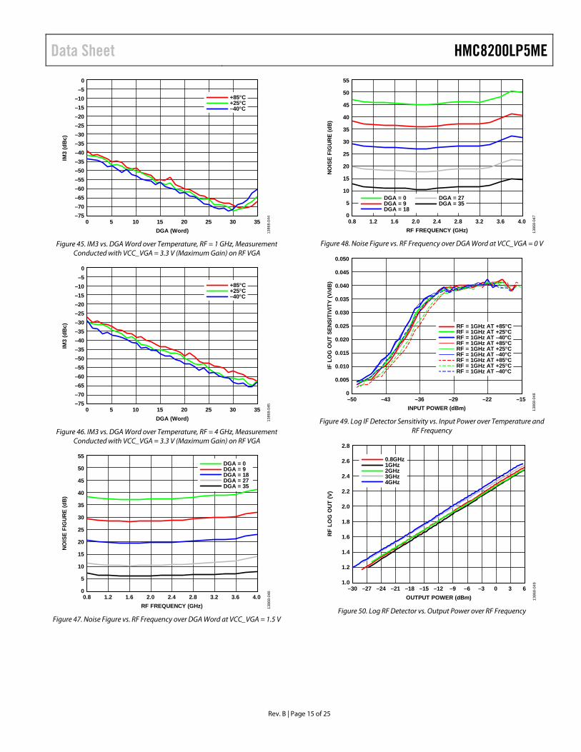
Figure 45. IM3 vs. DGA Word over Temperature, RF = 1 GHz, Measurement
Conducted with VCC_VGA = 3.3 V (Maximum Gain) on RF VGA
0–5
–10–15–20–25–30
–40–35
–35–50–55–60
–70–65
–75
IM3
(dB
c)
DGA (Word)0 5 10 20 3015 25 35
+85°C+25°C–40°C
1386
8-04
5
Figure 46. IM3 vs. DGA Word over Temperature, RF = 4 GHz, Measurement
Conducted with VCC_VGA = 3.3 V (Maximum Gain) on RF VGA
55
50
45
40
35
30
25
15
20
10
5
0
NO
ISE
FIG
UR
E (d
B)
RF FREQUENCY (GHz)0.8 1.2 1.6 2.4 3.22.0 2.8 3.6 4.0
DGA = 0DGA = 9DGA = 18DGA = 27DGA = 35
1386
8-04
6
Figure 47. Noise Figure vs. RF Frequency over DGA Word at VCC_VGA = 1.5 V
55
50
45
40
35
30
25
15
20
10
5
0
NO
ISE
FIG
UR
E (d
B)
RF FREQUENCY (GHz)0.8 1.2 1.6 2.4 3.22.0 2.8 3.6 4.0
DGA = 0DGA = 9DGA = 18
DGA = 27DGA = 35
1386
8-04
7
Figure 48. Noise Figure vs. RF Frequency over DGA Word at VCC_VGA = 0 V
0.050
0.045
0.040
0.035
0.030
0.025
0.020
0.010
0.015
0.005
0
IF L
OG
OU
T SE
NSI
TIVI
TY (V
/dB
)
INPUT POWER (dBm)–50 –43 –36 –22–29 –15
RF = 1GHz AT +85°CRF = 1GHz AT +25°CRF = 1GHz AT –40°CRF = 1GHz AT +85°CRF = 1GHz AT +25°CRF = 1GHz AT –40°CRF = 1GHz AT +85°CRF = 1GHz AT +25°CRF = 1GHz AT –40°C
1386
8-04
8
Figure 49. Log IF Detector Sensitivity vs. Input Power over Temperature and
RF Frequency
2.8
2.6
2.4
2.2
2.0
1.8
1.6
1.2
1.4
1.0
RF
LOG
OU
T (V
)
OUTPUT POWER (dBm)–30 –27 –24 –15 –3–21 –9 3–18 –6–12 0 6
0.8GHz1GHz2GHz3GHz4GHz
1386
8-04
9
Figure 50. Log RF Detector vs. Output Power over RF Frequency
HMC8200LP5ME Data Sheet
Rev. B | Page 16 of 25
2.5
2.0
1.5
1.0
0.5
0
IF L
OG
OU
T (V
)
INPUT POWER (dBm)–50 –45 –40 –25–35 –20–30 –15
RF = 1GHz AT +85°CRF = 1GHz AT +25°CRF = 1GHz AT –40°CRF = 1GHz AT +85°CRF = 1GHz AT +25°CRF = 1GHz AT –40°CRF = 1GHz AT +85°CRF = 1GHz AT +25°CRF = 1GHz AT –40°C
1386
8-05
0
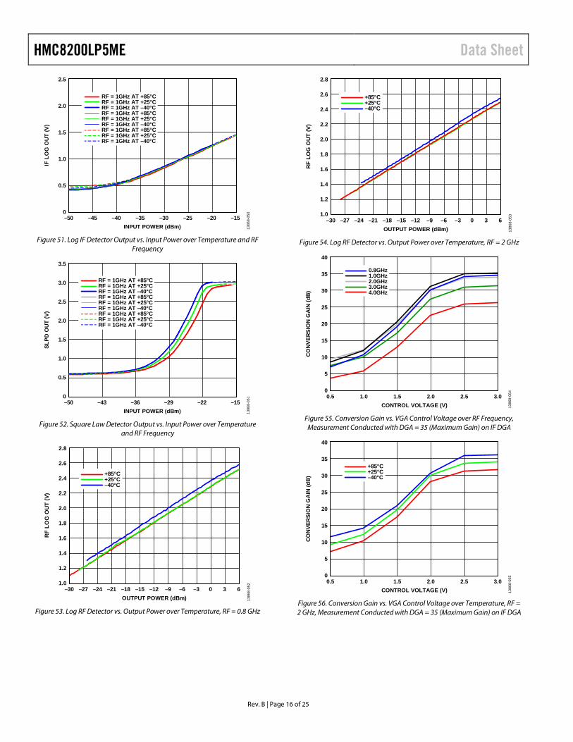
Figure 51. Log IF Detector Output vs. Input Power over Temperature and RF
Frequency
3.5
3.0
2.5
2.0
1.0
1.5
0.5
0
SLPD
OU
T (V
)
INPUT POWER (dBm)–50 –43 –36 –29 –22 –15
RF = 1GHz AT +85°CRF = 1GHz AT +25°CRF = 1GHz AT –40°CRF = 1GHz AT +85°CRF = 1GHz AT +25°CRF = 1GHz AT –40°CRF = 1GHz AT +85°CRF = 1GHz AT +25°CRF = 1GHz AT –40°C
1386
8-05
1
Figure 52. Square Law Detector Output vs. Input Power over Temperature
and RF Frequency
2.8
2.6
2.4
2.2
2.0
1.8
1.6
1.2
1.4
1.0
RF
LOG
OU
T (V
)
OUTPUT POWER (dBm)–30 –27 –24 –15 –3–21 –9 3–18 –6–12 0 6
+85°C+25°C–40°C
1386
8-05
2
Figure 53. Log RF Detector vs. Output Power over Temperature, RF = 0.8 GHz
2.8
2.6
2.4
2.2
1.0
1.6
1.4
1.2
1.8
2.0
–30 –24–27 –21 –18 –15 –12 –9 –6 –3 0 3 6
RF
LOG
OU
T (V
)
OUTPUT POWER (dBm)
+85°C+25°C–40°C
1386
8-05
3
Figure 54. Log RF Detector vs. Output Power over Temperature, RF = 2 GHz
40
35
30
0
15
10
5
20
25C
ON
VER
SIO
N G
AIN
(dB
)
CONTROL VOLTAGE (V)0.5 1.0 1.5 2.0 2.5 3.0
0.8GHz1.0GHz2.0GHz3.0GHz4.0GHz
1386
8-05
4
Figure 55. Conversion Gain vs. VGA Control Voltage over RF Frequency,
Measurement Conducted with DGA = 35 (Maximum Gain) on IF DGA
40
35
30
0
15
10
5
20
25
CO
NVE
RSI
ON
GA
IN (d
B)
CONTROL VOLTAGE (V)0.5 1.0 1.5 2.0 2.5 3.0
+85°C+25°C–40°C
1386
8-05
5
Figure 56. Conversion Gain vs. VGA Control Voltage over Temperature, RF = 2 GHz, Measurement Conducted with DGA = 35 (Maximum Gain) on IF DGA
Data Sheet HMC8200LP5ME
Rev. B | Page 17 of 25
2.8
2.6
2.4
2.2
1.0
1.6
1.4
1.2
1.8
2.0
–30 –24–27 –21 –18 –15 –12 –9 –6 –3 0 3 6
RF
LOG
OU
T (V
)
OUTPUT POWER (dBm)
+85°C+25°C–40°C
1386
8-05
6
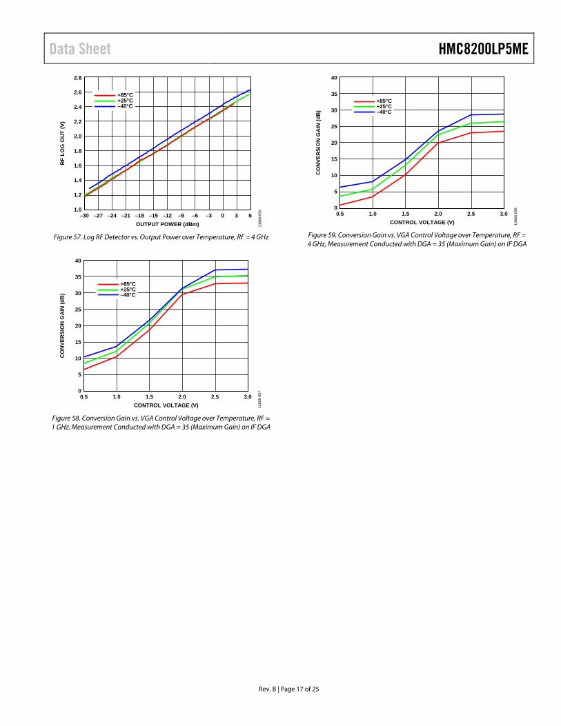
Figure 57. Log RF Detector vs. Output Power over Temperature, RF = 4 GHz
40
35
30
0
15
10
5
20
25
CO
NVE
RSI
ON
GA
IN (d
B)
CONTROL VOLTAGE (V)0.5 1.0 1.5 2.0 2.5 3.0
+85°C+25°C–40°C
1386
8-05
7
Figure 58. Conversion Gain vs. VGA Control Voltage over Temperature, RF = 1 GHz, Measurement Conducted with DGA = 35 (Maximum Gain) on IF DGA
40
35
30
0
15
10
5
20
25
CO
NVE
RSI
ON
GA
IN (d
B)
CONTROL VOLTAGE (V)0.5 1.0 1.5 2.0 2.5 3.0
+85°C+25°C–40°C
1386
8-05
8
Figure 59. Conversion Gain vs. VGA Control Voltage over Temperature, RF = 4 GHz, Measurement Conducted with DGA = 35 (Maximum Gain) on IF DGA
HMC8200LP5ME Data Sheet
Rev. B | Page 18 of 25
THEORY OF OPERATION TheHMC8200LP5ME is a highly integrated intermediate frequency (IF) transceiver chip that converts intermediate frequency to a single-ended radio frequency (RF) signal at its output. The intermediate frequency (IF) can be supplied to the HMC8200LP5ME singled ended or through the baseband differential inputs.
The single-ended input of the HMC8200LP5ME utilizes an input digital gain amplifier (DGA) that is controlled via SPI, which feeds the IF signals to an image reject mixer. At the input of the device before the DGA, an intermediate log power detector can be used to monitor input power levels into the device. A square law detector follows the DGA to monitor the power entering the mixer. See the Register Array Assignments and Serial Interface section for more information regarding the DGA.
The baseband differential inputs of the HMC8200LP5ME feed the intermediate frequency directly into the image reject mixer. It is recommended that when using the single-ended input, do not leave the baseband differential inputs connected. The local oscillator port can either be driven single ended through LO_N or differentially through the combination of LO_N and LO_P. If Driving the local oscillator port differentially improves the LO to RF rejection.
The IF is then converted to RF, which is followed by an amplifier. Next, the amplified RF signal is fed off chip to a low-pass filter. The external filter path feeds back into a variable gain amplifier (VGA) that is voltage controlled. The output of the VGA drives a final amplifier that is the output of the device. An RF log detector is connected to the output of the final amplifier to monitor the output power of the HMC8200LP5ME.
The HMC8200LP5ME utilizes an input low noise amplifier (LNA) cascaded with a VGA, which can either be controlled by the internal AGC or external voltages, that feeds the RF signals to an image reject mixer. The local oscillator port can either be driven single ended through LO_N or differentially through the combination of LO_N and LO_P.
The radio frequency is then converted to intermediate frequencies, which can either feed off chip via baseband differential outputs or feed on chip into a programmable band-pass filter. It is recommended during IF mode operation that the baseband outputs be unconnected.
The programmable band-pass filter on chip has four program-mable bandwidths (14 MHz, 28 MHz, 56 MHz, and 112 MHz). The programmable band-pass filter has the capability to adjust the center frequency.
From the factory, a filter calibration is conducted and the center frequency of the filter is set to 140 MHz. This calibration can be recalled via SPI control or the customer can adjust the center
frequency, but the calibration value must be stored off chip (see the Register Array Assignments section). An external filter option can be utilized to allow the customer to select other filter bandwidths/responses that are not available on chip. The external filter path coming from the image reject mixer feeds into an amplifier that has differential outputs. The output of the external filter can be fed back into the chip, which is then connected to another amplifier.
A VGA follows immediately after the band-pass filter. Control the IF VGA either by the AGC or external voltages. The output of the variable gain amplifier is the output of the device.
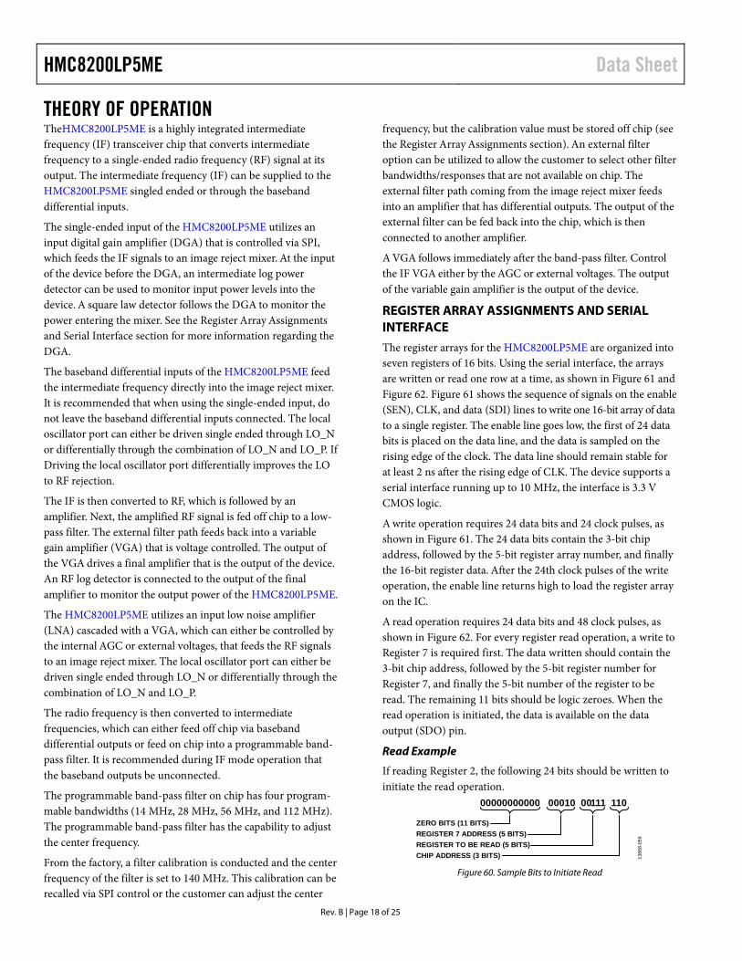
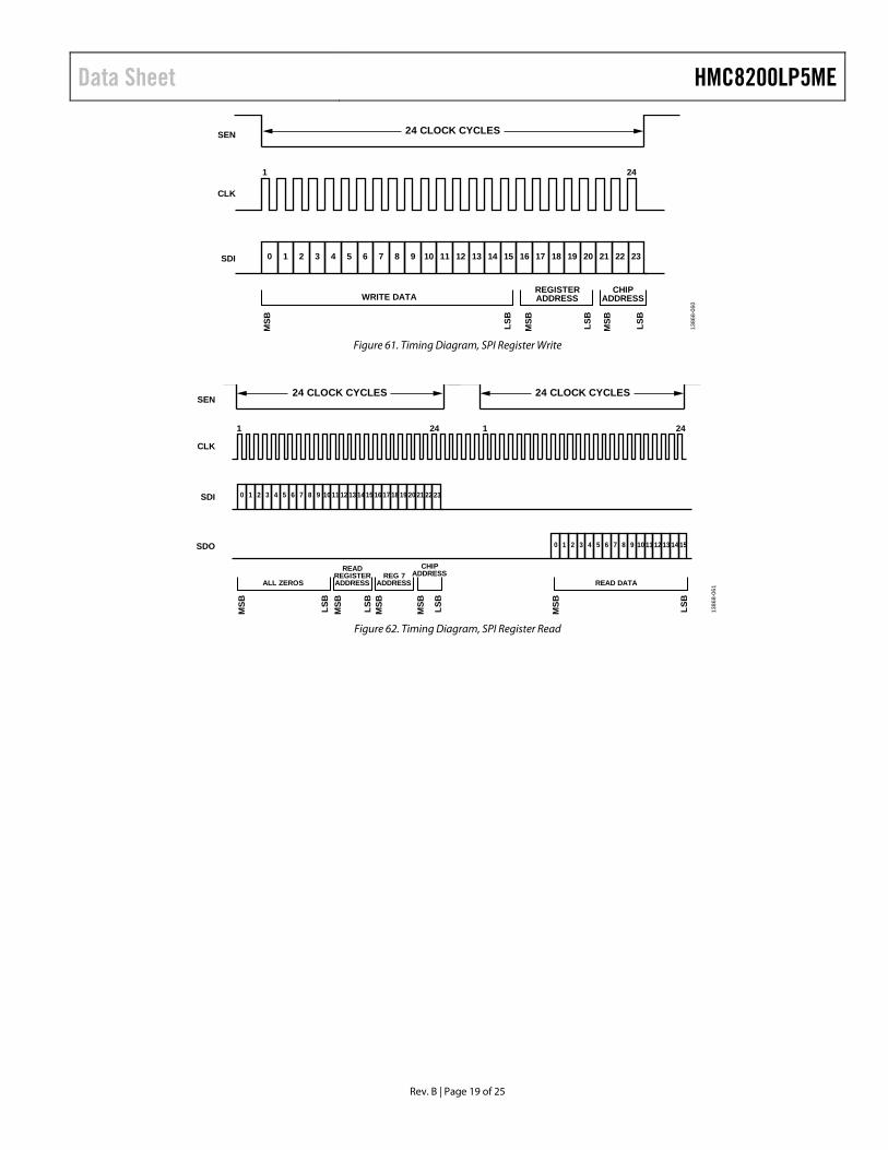
REGISTER ARRAY ASSIGNMENTS AND SERIAL INTERFACE The register arrays for the HMC8200LP5ME are organized into seven registers of 16 bits. Using the serial interface, the arrays are written or read one row at a time, as shown in Figure 61 and Figure 62. Figure 61 shows the sequence of signals on the enable (SEN), CLK, and data (SDI) lines to write one 16-bit array of data to a single register. The enable line goes low, the first of 24 data bits is placed on the data line, and the data is sampled on the rising edge of the clock. The data line should remain stable for at least 2 ns after the rising edge of CLK. The device supports a serial interface running up to 10 MHz, the interface is 3.3 V CMOS logic.
A write operation requires 24 data bits and 24 clock pulses, as shown in Figure 61. The 24 data bits contain the 3-bit chip address, followed by the 5-bit register array number, and finally the 16-bit register data. After the 24th clock pulses of the write operation, the enable line returns high to load the register array on the IC.
A read operation requires 24 data bits and 48 clock pulses, as shown in Figure 62. For every register read operation, a write to Register 7 is required first. The data written should contain the 3-bit chip address, followed by the 5-bit register number for Register 7, and finally the 5-bit number of the register to be read. The remaining 11 bits should be logic zeroes. When the read operation is initiated, the data is available on the data output (SDO) pin.
Read Example
If reading Register 2, the following 24 bits should be written to initiate the read operation.
00000000000 00010 00111 110
ZERO BITS (11 BITS)REGISTER 7 ADDRESS (5 BITS)REGISTER TO BE READ (5 BITS)CHIP ADDRESS (3 BITS) 13
868-
059
Figure 60. Sample Bits to Initiate Read
Data Sheet HMC8200LP5ME
Rev. B | Page 19 of 25
24 CLOCK CYCLESSEN
CLK
1 24
0 1 2 3 4 5 6 7 8 9 10 11 12 13 14 15 16 17 18 19 20 21 22 23SDI
WRITE DATAREGISTERADDRESS
CHIPADDRESS
MSB LS
B
MSB LS
B
LSB
MSB
1386
8-06
0
Figure 61. Timing Diagram, SPI Register Write
24 CLOCK CYCLES 24 CLOCK CYCLES
SEN
1 124 24
ALL ZEROS READ DATA
READREGISTERADDRESS
REG 7ADDRESS
CHIPADDRESS
CLK
SDI
SDO
MSB LS
BM
SB LSB
MSB LS
B
MSB LS
B
MSB
0 1 2 3 4 5 6 7 8 9 10 11 12 13 14 15 16 17 18 19 20 21 22 23
0 1 2 3 4 5 6 7 8 9 10 11 12 13 14 15
1386
8-06
1
Figure 62. Timing Diagram, SPI Register Read
HMC8200LP5ME Data Sheet
Rev. B | Page 20 of 25
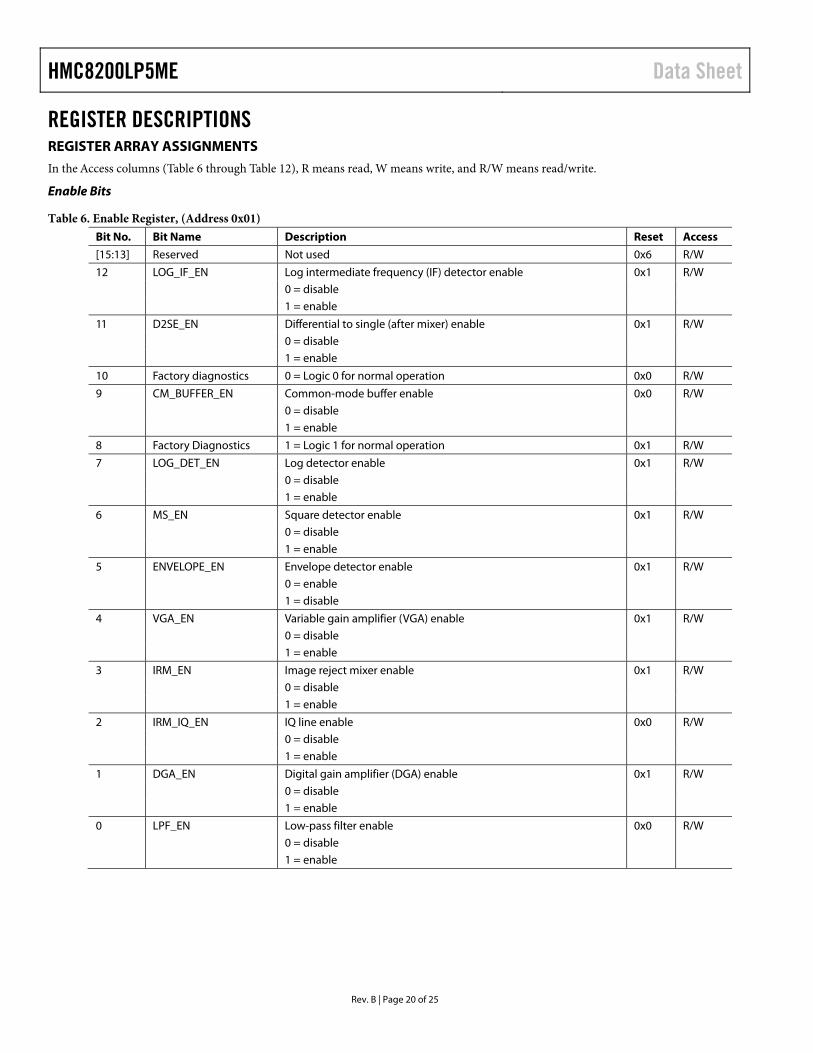
REGISTER DESCRIPTIONS REGISTER ARRAY ASSIGNMENTS In the Access columns (Table 6 through Table 12), R means read, W means write, and R/W means read/write.
Enable Bits
Table 6. Enable Register, (Address 0x01) Bit No. Bit Name Description Reset Access [15:13] Reserved Not used 0x6 R/W 12 LOG_IF_EN Log intermediate frequency (IF) detector enable 0x1 R/W 0 = disable 1 = enable 11 D2SE_EN Differential to single (after mixer) enable 0x1 R/W 0 = disable 1 = enable 10 Factory diagnostics 0 = Logic 0 for normal operation 0x0 R/W 9 CM_BUFFER_EN Common-mode buffer enable 0x0 R/W 0 = disable 1 = enable 8 Factory Diagnostics 1 = Logic 1 for normal operation 0x1 R/W 7 LOG_DET_EN Log detector enable 0x1 R/W 0 = disable 1 = enable 6 MS_EN Square detector enable 0x1 R/W 0 = disable 1 = enable 5 ENVELOPE_EN Envelope detector enable 0x1 R/W 0 = enable 1 = disable 4 VGA_EN Variable gain amplifier (VGA) enable 0x1 R/W 0 = disable 1 = enable 3 IRM_EN Image reject mixer enable 0x1 R/W 0 = disable 1 = enable 2 IRM_IQ_EN IQ line enable 0x0 R/W 0 = disable 1 = enable 1 DGA_EN Digital gain amplifier (DGA) enable 0x1 R/W 0 = disable 1 = enable 0 LPF_EN Low-pass filter enable 0x0 R/W 0 = disable 1 = enable
Data Sheet HMC8200LP5ME
Rev. B | Page 21 of 25
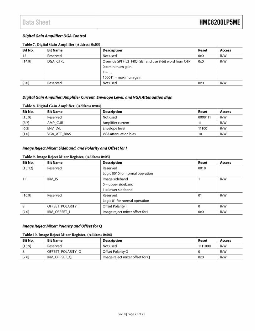
Digital Gain Amplifier: DGA Control
Table 7. Digital Gain Amplifier (Address 0x03) Bit No. Bit Name Description Reset Access 15 Reserved Not used 0x0 R/W [14:9] DGA_CTRL Override SPI FIL2_FRQ_SET and use 8-bit word from OTP 0x0 R/W 0 = minimum gain 1 = … 100011 = maximum gain [8:0] Reserved Not used 0x0 R/W
Digital Gain Amplifier: Amplifier Current, Envelope Level, and VGA Attenuation Bias
Table 8. Digital Gain Amplifier, (Address 0x04) Bit No. Bit Name Description Reset Access [15:9] Reserved Not used 0000111 R/W [8:7] AMP_CUR Amplifier current 11 R/W [6:2] ENV_LVL Envelope level 11100 R/W [1:0] VGA_ATT_BIAS VGA attenuation bias 10 R/W
Image Reject Mixer: Sideband, and Polarity and Offset for I
Table 9. Image Reject Mixer Register, (Address 0x05) Bit No. Bit Name Description Reset Access [15:12] Reserved Reserved 0010 Logic 0010 for normal operation 11 IRM_IS Image sideband 1 R/W 0 = upper sideband 1 = lower sideband [10:9] Reserved Reserved 01 R/W Logic 01 for normal operation 8 OFFSET_POLARITY_I Offset Polarity I 0 R/W [7:0] IRM_OFFSET_I Image reject mixer offset for I 0x0 R/W
Image Reject Mixer: Polarity and Offset for Q
Table 10. Image Reject Mixer Register, (Address 0x06) Bit No. Bit Name Description Reset Access [15:9] Reserved Not used 1111000 R/W 8 OFFSET_POLARITY_Q Offset Polarity Q 0 R/W [7:0] IRM_OFFSET_Q Image reject mixer offset for Q 0x0 R/W
HMC8200LP5ME Data Sheet
Rev. B | Page 22 of 25
Phase I: Adjust
Table 11. Phase I Register, (Address 0x08) Bit No. Bit Name Description Reset Access [15:9] Reserved Not used 1111000 R/W [8:0] I_PHASE_ADJ I phase adjust 0x0 R/W
Phase Q: Adjust
Table 12. Phase Q Register, (Address 0x09) Bit No. Bit Name Description Reset Access [15:9] Reserved Not used 1111000 R/W [8:0] Q_PHASE_ADJ Q phase adjust 0x0 R/W
Data Sheet HMC8200LP5ME
Rev. B | Page 23 of 25
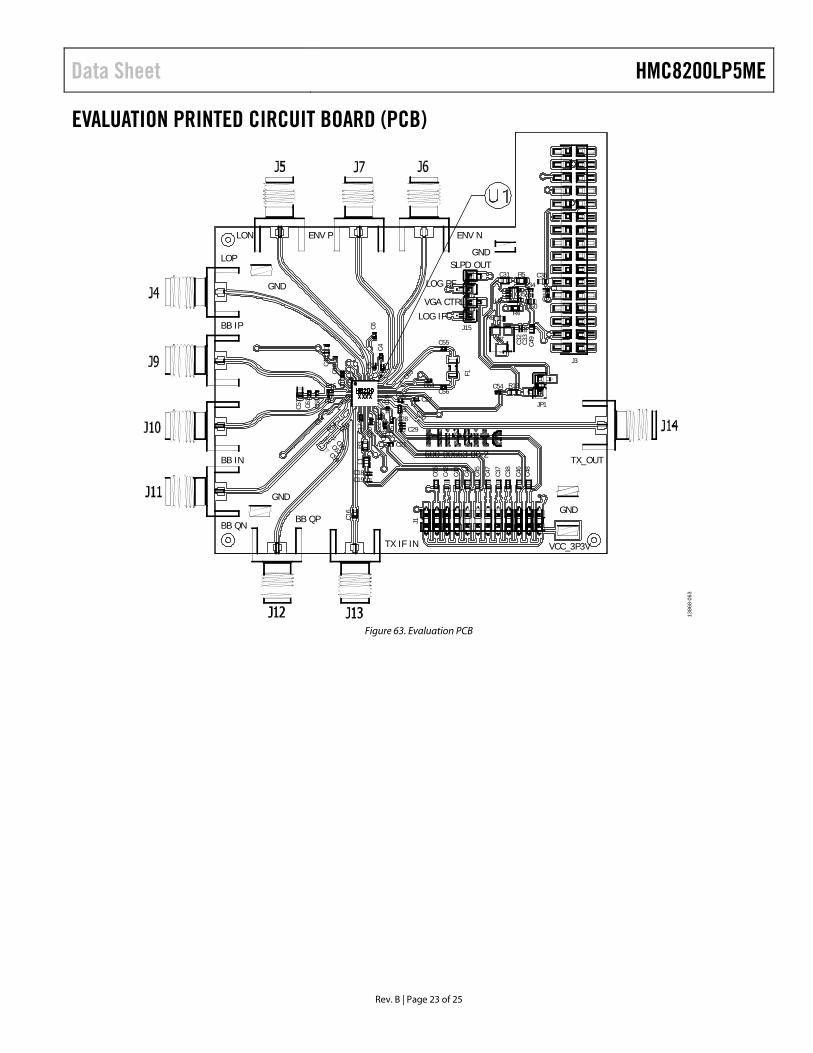
EVALUATION PRINTED CIRCUIT BOARD (PCB)
LOG IF
BB QPGND
GND
GND
VCC_3P3V
GND
BB IP
TX_OUT
VGA CTRL
LOG RF
SLPD OUT
ENV NENV PLON
LOP
BB IN
TX IF IN
BB QN
600-00663-00-2
C56
C55
C61
C62
C65
C64C6
3
R16
J1
R3
R14
C57
C59
C58
C60
J15
R13C54
R17
R15
C50
C49
C48
C45
C47
C46
C43
C42
C21
C40
C38
C37
C36
C6C4
C35
C33
C29
C23
C27C2
5
C19
C14
C44
C10
C1
L1
L2
C31
C16
C5
C28
C17
C11
JP1
J3
R4
R5
R6
R7
F1C18
C15
C20
C26
C32
C34
C24
C30
C22
C3
C2U2
1386
8-06
3
Figure 63. Evaluation PCB
HMC8200LP5ME Data Sheet
Rev. B | Page 24 of 25
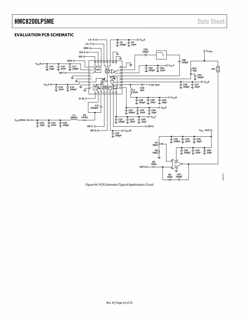
EVALUATION PCB SCHEMATIC
1718192021222324
LO_N
LO_P
SEN
SCLK
SDI
SPI
SDO
RST
VCC9
VCC2
VCC3
C4010µF
C1010nF
C1410nF
C15100pF
C171000pF
C5100pF
C610nF
VCC4C63100pF
C6410nF
C28100pF
C2910nF
C4810µF
C11100pF
C24100pF
C2510nF
C4610µF
C55100pF
C31100pF
C56100pF
C54100pF
R131kΩ
VCC5
JP1
C26100pF
C2710nFC30
5pF
RF OUT
L215nH
IF IN VCC8
VCC6
C22100pF
C20100pF
C2310nF
C4510µF
VCC7
DET3
DET2
DET1
VCC10
R324.9Ω
L1330nH
VCC1/DGA_S1C4310µF
C1910nF
C18100pF
VCTRL
R510kΩ
R510kΩ
DET3
C34100pF
C3310nF
C5010µF
C32100pF
C3310nF
C4910µF
VCC_AGC
R710kΩ
R610kΩ
3
4
5VV
2
1
2526272829303132
1
34
2
5678
9 121110 13 14 15 16
1386
8-06
2
Figure 64. PCB Schematic/Typical Applications Circuit
Data Sheet HMC8200LP5ME
Rev. B | Page 25 of 25
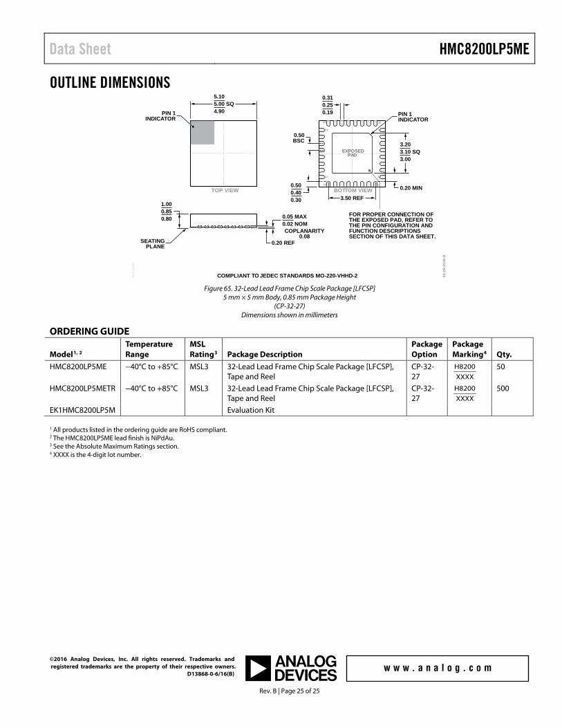
OUTLINE DIMENSIONS
02-2
6-20
16-A
1
0.50BSC
BOTTOM VIEWTOP VIEW
PIN 1INDICATOR
32
916
17
24
25
8
PIN 1INDICATOR
SEATINGPLANE
0.05 MAX0.02 NOM
0.20 REF
COPLANARITY0.08
0.310.250.19
5.105.00 SQ4.90
FOR PROPER CONNECTION OFTHE EXPOSED PAD, REFER TOTHE PIN CONFIGURATION ANDFUNCTION DESCRIPTIONSSECTION OF THIS DATA SHEET.
0.500.400.30
1.000.850.80
0.20 MIN
3.203.10 SQ3.00
PKG
-000
000
3.50 REF
COMPLIANT TO JEDEC STANDARDS MO-220-VHHD-2
EXPOSEDPAD
Figure 65. 32-Lead Lead Frame Chip Scale Package [LFCSP]
5 mm × 5 mm Body, 0.85 mm Package Height (CP-32-27)
Dimensions shown in millimeters
ORDERING GUIDE
Model1, 2 Temperature Range
MSL Rating3 Package Description
Package Option
Package Marking4 Qty.
HMC8200LP5ME −40°C to +85°C MSL3 32-Lead Lead Frame Chip Scale Package [LFCSP], Tape and Reel
CP-32-27 XXXX
H8200 50
HMC8200LP5METR −40°C to +85°C MSL3 32-Lead Lead Frame Chip Scale Package [LFCSP], Tape and Reel
CP-32-27 XXXX
H8200 500
EK1HMC8200LP5M Evaluation Kit 1 All products listed in the ordering guide are RoHS compliant. 2 The HMC8200LP5ME lead finish is NiPdAu. 3 See the Absolute Maximum Ratings section. 4 XXXX is the 4-digit lot number.
©2016 Analog Devices, Inc. All rights reserved. Trademarks and registered trademarks are the property of their respective owners. D13868-0-6/16(B)