Embed Size (px)
Citation preview
Interference effects on indium tin oxide enhanced Raman scattering
Yimin Yang,1,a) Teng Qiu,1,a) Fan Kong,2 Jiyang Fan,1 Huiling Ou,1 Qingyu Xu,1
and Paul K. Chu3
1Department of Physics, Southeast University, Nanjing 211189, People’s Republic of China2School of Chemistry and Chemical Engineering, Southeast University, Nanjing 211189, People’s Republicof China3Department of Physics and Materials Science, City University of Hong Kong, Tat Chee Avenue, Kowloon,Hong Kong, China
(Received 21 October 2011; accepted 12 January 2012; published online 14 February 2012)
Optical interference is known to alter the intensity of Raman scattering signals. Its effect on
enhanced Raman scattering from embedded indium tin oxide (ITO) nano-island arrays prepared by
pulsed laser deposition of ITO films with different thicknesses on Si templates with nano-scale
roughness are studied. Optical self-interference of the incident, scattered, and emitted light is
observed to modulate the intensity and shape of the Raman signals as well as fluorescence
background. The fluctuations in the Raman signals and fluorescence background can be explained
by a theoretical model considering multiple reflections at the surface and interface. This
interference effect must be taken into account in the investigation of enhanced Raman scattering
from ITO. VC 2012 American Institute of Physics. [doi:10.1063/1.3684965]
I. INTRODUCTION
Transparent conductive oxides such as indium tin oxide
(ITO) have attracted significant interest in recent years for
potential applications in surface plasmon resonance (SPR)
based sensing and surface-enhanced spectroscopy.1–4 It has
been reported that the SPR from ITO resembles that of noble
metals and is free from interference from interband transi-
tions.5,6 However, fabrication of nanostructured ITO surfa-
ces with evenly distributed plasmonic fields and reliable SPR
properties is still challenging, and more research is needed to
enable wider use of ITO in chemical and biological sensing.
We have recently reported surface-enhanced Raman scat-
tering (SERS) from embedded ITO nanoisland arrays pre-
pared by pulsed laser deposition of ITO films on Si templates
with a roughened surface.4 Because of the optical transpar-
ency and chemical stability, the functional ITO layer is pro-
tected at the interface and not prone to contamination and
other undesirable surface activities. Considerable Raman
enhancement is observed during Arþ laser irradiation, and the
effect is modulated by the thickness of the ITO film due to the
exponentially decaying field of the localized SPR at the inter-
face. The interference phenomenon observed from ITO/Si
substrates, however, influences the intensity of the Raman sig-
nals, but this topic has not been studied systematically. This
interference phenomenon usually occurs between the surface
and interface of a transparent film with a thickness between
several nanometers and micrometers.7,8 In fact, in previous
studies pertaining to the enhancement of Raman signals using
the interference phenomenon, an enhancement factor of up to
30 was observed.9–11 In this work, the influence of the inter-
ference phenomenon is investigated on ITO films having
thicknesses in the range of 40-480 nm. Periodical fluctuations
in the intensity of Raman signals and fluorescence background
are observed, and a theoretical model is proposed to elucidate
the mechanism.
II. EXPERIMENTAL
Si templates with nano-scale roughness were formed on
p-type (100) Si wafers (1-60 X-cm) by wet etching in a
15 wt. % NaOH solution at 30 �C for 8 min. High-density
and randomly distributed Si islands can be observed from
the Si surface after etching according to the AFM (Veeco
Multimode) image depicted in Fig. 1 and our previous
work.4 The embedded ITO (In2O3 92 wt. %, SnO2 8 wt. %)
nano-island arrays on the Si templates were prepared by
pulsed laser deposition (248 nm KrF laser, 300 mJ/pulse,
3.0 Pa oxygen) at room temperature. To improve crystalliza-
tion and conductivity, the samples were annealed at 550 �Cin vacuum (2� 10�3 Pa) for 30 min. The crystal structure of
the ITO film was characterized by x-ray diffraction (XRD,
Bruker) on a 350 nm thick ITO film. The result (not shown
here) indicates that the annealed ITO films retain the cubic
crystal structure of In2O3 and the ITO grains with an average
size of 40 nm (Scherrer equation) are randomly distributed.
A 10�5 M aqueous rhodamine 6 G (R6 G) solution was
used to evaluate the Raman enhancement effect, and the sam-
ples were kept in the R6 G solution for 40 min before mea-
surement. The SERS measurements were performed at room
temperature on a Horiba Jobin-Yvon LabRAM HR800 micro-
Raman spectrometer with a 514 nm laser focused to a diame-
ter of 1 lm. The incident power was 0.55 mW and acquisition
time was 10 s. Koehler illumination was adopted to acquire
on-site reflective optical images of the ITO/Si samples.
The refractive index (n), extinction coefficient (j), and
thickness (d) of the ITO films were measured from the
s-polarization reflective spectra of the ITO/Si samples and Si
wafer on a spectrometer equipped with a Xe lamp and Iceland
spar polarizer at an incident angle of 45�. Figure 2 shows
the representative s-polarization reflectivity ratio RITO/Si/RSi
a)Authors to whom correspondence should be addressed. Electronic
addresses: [email protected] and [email protected].
0021-8979/2012/111(3)/033110/4/$30.00 VC 2012 American Institute of Physics111, 033110-1
JOURNAL OF APPLIED PHYSICS 111, 033110 (2012)
spectrum of a ITO(650 nm)/Si sample and Si wafer. The re-
fractive index and extinction coefficient of the ITO film were
obtained based on the optical interference theory.12 The thick-
ness distribution of ITO films was determined from the
s-polarization reflective spectra and the obtained refractive
index curve in Fig. 2.
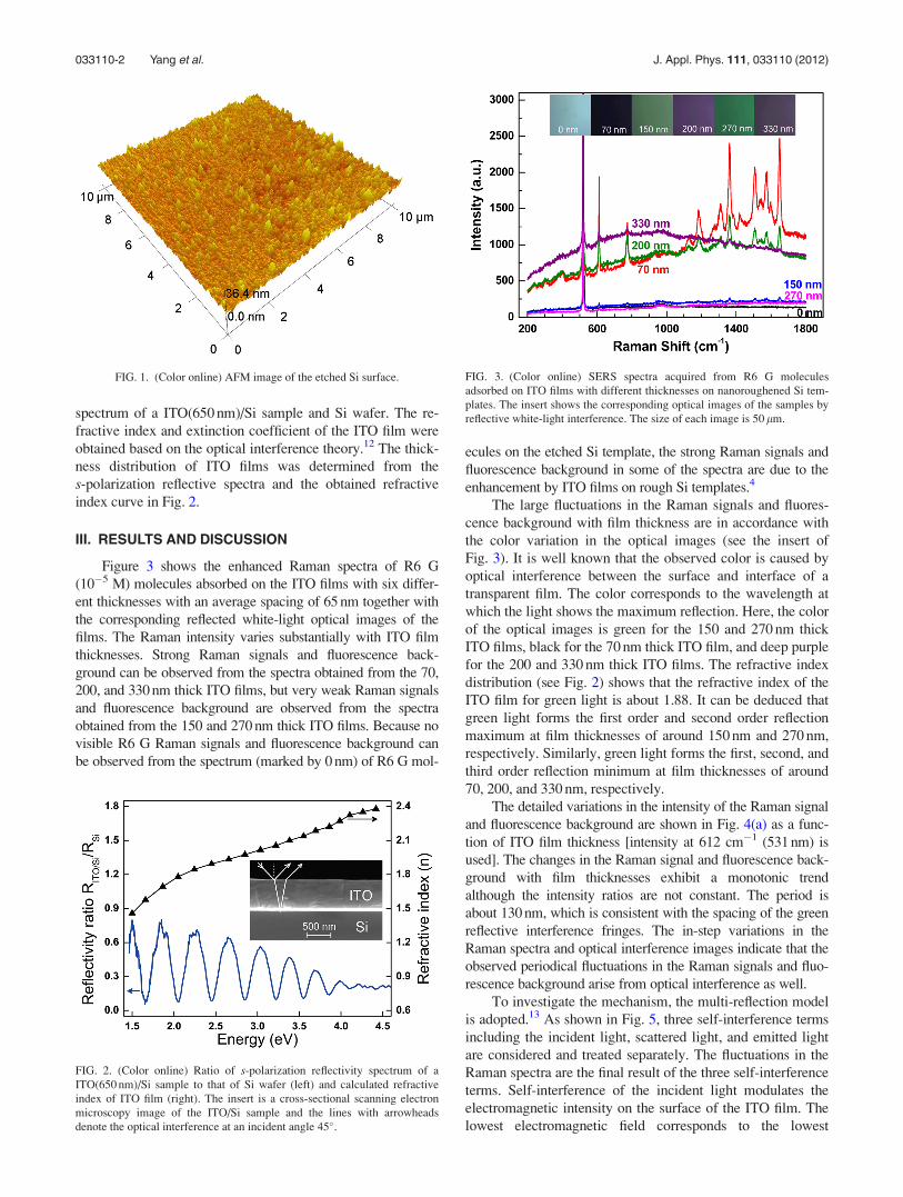
III. RESULTS AND DISCUSSION
Figure 3 shows the enhanced Raman spectra of R6 G
(10�5 M) molecules absorbed on the ITO films with six differ-
ent thicknesses with an average spacing of 65 nm together with
the corresponding reflected white-light optical images of the
films. The Raman intensity varies substantially with ITO film
thicknesses. Strong Raman signals and fluorescence back-
ground can be observed from the spectra obtained from the 70,
200, and 330 nm thick ITO films, but very weak Raman signals
and fluorescence background are observed from the spectra
obtained from the 150 and 270 nm thick ITO films. Because no
visible R6 G Raman signals and fluorescence background can
be observed from the spectrum (marked by 0 nm) of R6 G mol-
ecules on the etched Si template, the strong Raman signals and
fluorescence background in some of the spectra are due to the
enhancement by ITO films on rough Si templates.4
The large fluctuations in the Raman signals and fluores-
cence background with film thickness are in accordance with
the color variation in the optical images (see the insert of
Fig. 3). It is well known that the observed color is caused by
optical interference between the surface and interface of a
transparent film. The color corresponds to the wavelength at
which the light shows the maximum reflection. Here, the color
of the optical images is green for the 150 and 270 nm thick
ITO films, black for the 70 nm thick ITO film, and deep purple
for the 200 and 330 nm thick ITO films. The refractive index
distribution (see Fig. 2) shows that the refractive index of the
ITO film for green light is about 1.88. It can be deduced that
green light forms the first order and second order reflection
maximum at film thicknesses of around 150 nm and 270 nm,
respectively. Similarly, green light forms the first, second, and
third order reflection minimum at film thicknesses of around
70, 200, and 330 nm, respectively.
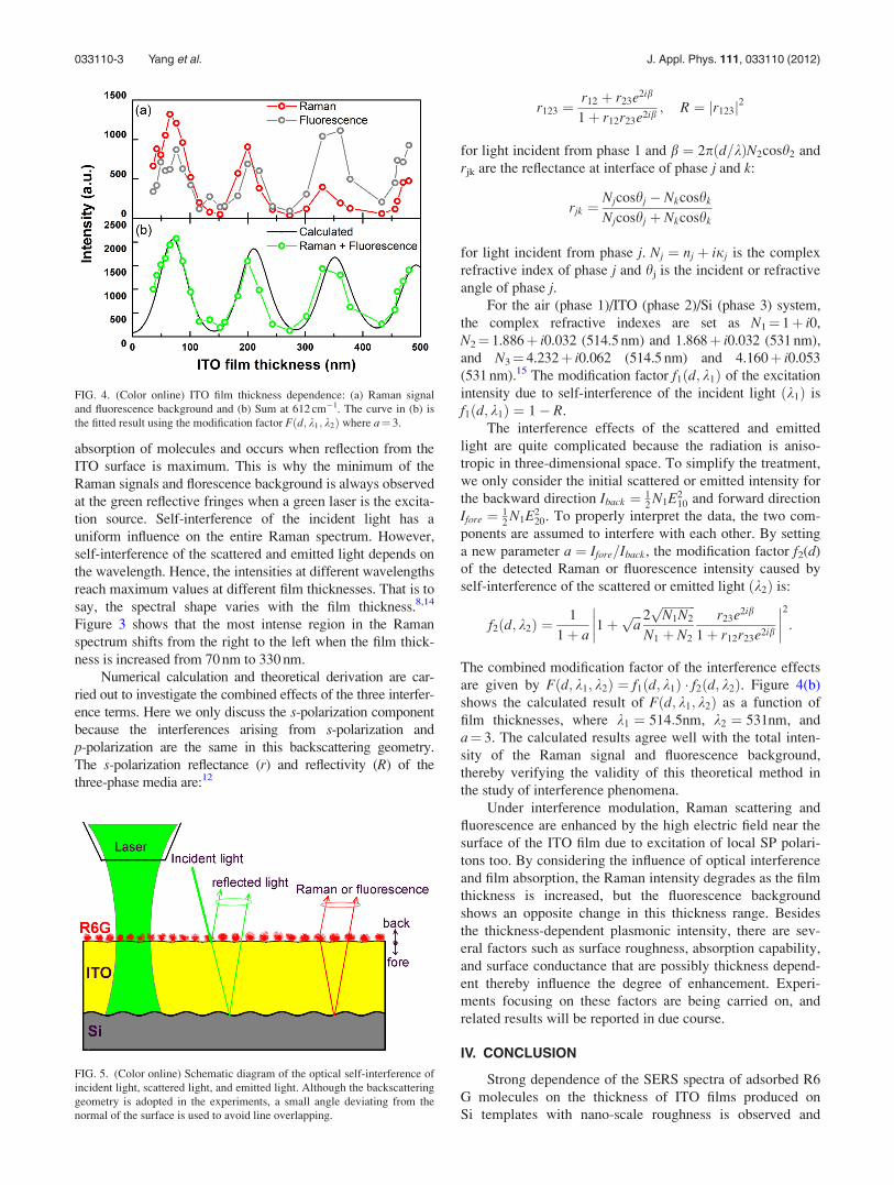
The detailed variations in the intensity of the Raman signal
and fluorescence background are shown in Fig. 4(a) as a func-
tion of ITO film thickness [intensity at 612 cm�1 (531 nm) is
used]. The changes in the Raman signal and fluorescence back-
ground with film thicknesses exhibit a monotonic trend
although the intensity ratios are not constant. The period is
about 130 nm, which is consistent with the spacing of the green
reflective interference fringes. The in-step variations in the
Raman spectra and optical interference images indicate that the
observed periodical fluctuations in the Raman signals and fluo-
rescence background arise from optical interference as well.
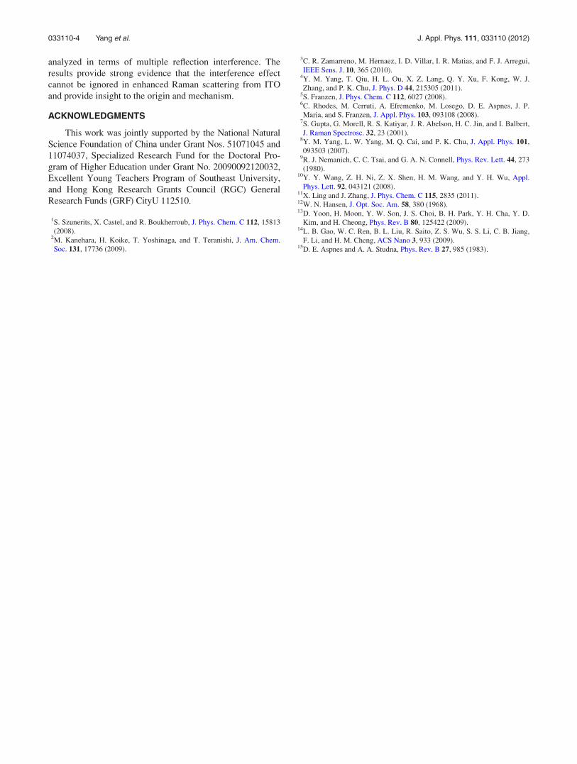
To investigate the mechanism, the multi-reflection model
is adopted.13 As shown in Fig. 5, three self-interference terms
including the incident light, scattered light, and emitted light
are considered and treated separately. The fluctuations in the
Raman spectra are the final result of the three self-interference
terms. Self-interference of the incident light modulates the
electromagnetic intensity on the surface of the ITO film. The
lowest electromagnetic field corresponds to the lowest
FIG. 1. (Color online) AFM image of the etched Si surface.
FIG. 2. (Color online) Ratio of s-polarization reflectivity spectrum of a
ITO(650 nm)/Si sample to that of Si wafer (left) and calculated refractive
index of ITO film (right). The insert is a cross-sectional scanning electron
microscopy image of the ITO/Si sample and the lines with arrowheads
denote the optical interference at an incident angle 45�.
FIG. 3. (Color online) SERS spectra acquired from R6 G molecules
adsorbed on ITO films with different thicknesses on nanoroughened Si tem-
plates. The insert shows the corresponding optical images of the samples by
reflective white-light interference. The size of each image is 50 lm.
033110-2 Yang et al. J. Appl. Phys. 111, 033110 (2012)
absorption of molecules and occurs when reflection from the
ITO surface is maximum. This is why the minimum of the
Raman signals and florescence background is always observed
at the green reflective fringes when a green laser is the excita-
tion source. Self-interference of the incident light has a
uniform influence on the entire Raman spectrum. However,
self-interference of the scattered and emitted light depends on
the wavelength. Hence, the intensities at different wavelengths
reach maximum values at different film thicknesses. That is to
say, the spectral shape varies with the film thickness.8,14
Figure 3 shows that the most intense region in the Raman
spectrum shifts from the right to the left when the film thick-
ness is increased from 70 nm to 330 nm.
Numerical calculation and theoretical derivation are car-
ried out to investigate the combined effects of the three interfer-
ence terms. Here we only discuss the s-polarization component
because the interferences arising from s-polarization and
p-polarization are the same in this backscattering geometry.
The s-polarization reflectance (r) and reflectivity (R) of the
three-phase media are:12
r123 ¼r12 þ r23e2ib
1þ r12r23e2ib; R ¼ jr123j2
for light incident from phase 1 and b ¼ 2pðd=kÞN2cosh2 and
rjk are the reflectance at interface of phase j and k:
rjk ¼Njcoshj � Nkcoshk
Njcoshj þ Nkcoshk
for light incident from phase j. Nj ¼ nj þ ijj is the complex
refractive index of phase j and hj is the incident or refractive
angle of phase j.For the air (phase 1)/ITO (phase 2)/Si (phase 3) system,
the complex refractive indexes are set as N1¼ 1þ i0,
N2¼ 1.886þ i0.032 (514.5 nm) and 1.868þ i0.032 (531 nm),
and N3¼ 4.232þ i0.062 (514.5 nm) and 4.160þ i0.053
(531 nm).15 The modification factor f1ðd; k1Þ of the excitation
intensity due to self-interference of the incident light ðk1Þ is
f1ðd; k1Þ ¼ 1� R.
The interference effects of the scattered and emitted
light are quite complicated because the radiation is aniso-
tropic in three-dimensional space. To simplify the treatment,
we only consider the initial scattered or emitted intensity for
the backward direction Iback ¼ 12
N1E210 and forward direction
Ifore ¼ 12
N1E220. To properly interpret the data, the two com-
ponents are assumed to interfere with each other. By setting
a new parameter a ¼ Ifore=Iback, the modification factor f2(d)
of the detected Raman or fluorescence intensity caused by
self-interference of the scattered or emitted light ðk2Þ is:
f2ðd; k2Þ ¼1
1þ a
����1þ
ffiffiffiap 2
ffiffiffiffiffiffiffiffiffiffiffiN1N2
p
N1 þ N2
r23e2ib
1þ r12r23e2ib
����
2
:
The combined modification factor of the interference effects
are given by Fðd; k1; k2Þ ¼ f1ðd; k1Þ � f2ðd; k2Þ. Figure 4(b)
shows the calculated result of Fðd; k1; k2Þ as a function of
film thicknesses, where k1 ¼ 514:5nm, k2 ¼ 531nm, and
a¼ 3. The calculated results agree well with the total inten-
sity of the Raman signal and fluorescence background,
thereby verifying the validity of this theoretical method in
the study of interference phenomena.
Under interference modulation, Raman scattering and
fluorescence are enhanced by the high electric field near the
surface of the ITO film due to excitation of local SP polari-
tons too. By considering the influence of optical interference
and film absorption, the Raman intensity degrades as the film
thickness is increased, but the fluorescence background
shows an opposite change in this thickness range. Besides
the thickness-dependent plasmonic intensity, there are sev-
eral factors such as surface roughness, absorption capability,
and surface conductance that are possibly thickness depend-
ent thereby influence the degree of enhancement. Experi-
ments focusing on these factors are being carried on, and
related results will be reported in due course.
IV. CONCLUSION
Strong dependence of the SERS spectra of adsorbed R6
G molecules on the thickness of ITO films produced on
Si templates with nano-scale roughness is observed and
FIG. 4. (Color online) ITO film thickness dependence: (a) Raman signal
and fluorescence background and (b) Sum at 612 cm�1. The curve in (b) is
the fitted result using the modification factor Fðd; k1; k2Þ where a¼ 3.
FIG. 5. (Color online) Schematic diagram of the optical self-interference of
incident light, scattered light, and emitted light. Although the backscattering
geometry is adopted in the experiments, a small angle deviating from the
normal of the surface is used to avoid line overlapping.
033110-3 Yang et al. J. Appl. Phys. 111, 033110 (2012)
analyzed in terms of multiple reflection interference. The
results provide strong evidence that the interference effect
cannot be ignored in enhanced Raman scattering from ITO
and provide insight to the origin and mechanism.
ACKNOWLEDGMENTS
This work was jointly supported by the National Natural
Science Foundation of China under Grant Nos. 51071045 and
11074037, Specialized Research Fund for the Doctoral Pro-
gram of Higher Education under Grant No. 20090092120032,
Excellent Young Teachers Program of Southeast University,
and Hong Kong Research Grants Council (RGC) General
Research Funds (GRF) CityU 112510.
1S. Szunerits, X. Castel, and R. Boukherroub, J. Phys. Chem. C 112, 15813
(2008).2M. Kanehara, H. Koike, T. Yoshinaga, and T. Teranishi, J. Am. Chem.
Soc. 131, 17736 (2009).
3C. R. Zamarreno, M. Hernaez, I. D. Villar, I. R. Matias, and F. J. Arregui,
IEEE Sens. J. 10, 365 (2010).4Y. M. Yang, T. Qiu, H. L. Ou, X. Z. Lang, Q. Y. Xu, F. Kong, W. J.
Zhang, and P. K. Chu, J. Phys. D 44, 215305 (2011).5S. Franzen, J. Phys. Chem. C 112, 6027 (2008).6C. Rhodes, M. Cerruti, A. Efremenko, M. Losego, D. E. Aspnes, J. P.
Maria, and S. Franzen, J. Appl. Phys. 103, 093108 (2008).7S. Gupta, G. Morell, R. S. Katiyar, J. R. Abelson, H. C. Jin, and I. Balbert,
J. Raman Spectrosc. 32, 23 (2001).8Y. M. Yang, L. W. Yang, M. Q. Cai, and P. K. Chu, J. Appl. Phys. 101,
093503 (2007).9R. J. Nemanich, C. C. Tsai, and G. A. N. Connell, Phys. Rev. Lett. 44, 273
(1980).10Y. Y. Wang, Z. H. Ni, Z. X. Shen, H. M. Wang, and Y. H. Wu, Appl.
Phys. Lett. 92, 043121 (2008).11X. Ling and J. Zhang, J. Phys. Chem. C 115, 2835 (2011).12W. N. Hansen, J. Opt. Soc. Am. 58, 380 (1968).13D. Yoon, H. Moon, Y. W. Son, J. S. Choi, B. H. Park, Y. H. Cha, Y. D.
Kim, and H. Cheong, Phys. Rev. B 80, 125422 (2009).14L. B. Gao, W. C. Ren, B. L. Liu, R. Saito, Z. S. Wu, S. S. Li, C. B. Jiang,
F. Li, and H. M. Cheng, ACS Nano 3, 933 (2009).15D. E. Aspnes and A. A. Studna, Phys. Rev. B 27, 985 (1983).
033110-4 Yang et al. J. Appl. Phys. 111, 033110 (2012)


![Enhanced Inter-Cell Interference Coordination Challenges in ... · arXiv:1112.1597v1 [cs.NI] 7 Dec 2011 1 Enhanced Inter-Cell Interference Coordination Challenges in Heterogeneous](https://img.dokumen.tips/doc/110x75/6041cc39bf45693f576428a5/enhanced-inter-cell-interference-coordination-challenges-in-arxiv11121597v1.jpg)