Embed Size (px)
Citation preview
Intel® Pentium® M Processor with 2-MB L2 Cache and 533-MHz Front Side BusDatasheet
July 2005
Reference Number: 305262-002
2 Datasheet
INFORMATION IN THIS DOCUMENT IS PROVIDED IN CONNECTION WITH INTEL PRODUCTS. NO LICENSE, EXPRESS OR IMPLIED, BY ESTOPPEL OR OTHERWISE, TO ANY INTELLECTUAL PROPERTY RIGHTS IS GRANTED BY THIS DOCUMENT. EXCEPT AS PROVIDED IN INTEL’S TERMS AND CONDITIONS OF SALE FOR SUCH PRODUCTS, INTEL ASSUMES NO LIABILITY WHATSOEVER, AND INTEL DISCLAIMS ANY EXPRESS OR IMPLIED WARRANTY, RELATING TO SALE AND/OR USE OF INTEL PRODUCTS INCLUDING LIABILITY OR WARRANTIES RELATING TO FITNESS FOR A PARTICULAR PURPOSE, MERCHANTABILITY, OR INFRINGEMENT OF ANY PATENT, COPYRIGHT OR OTHER INTELLECTUAL PROPERTY RIGHT. Intel products are not intended for use in medical, life saving, or life sustaining applications.
Intel may make changes to specifications and product descriptions at any time, without notice.
Designers must not rely on the absence or characteristics of any features or instructions marked “reserved” or “undefined.” Intel reserves these for future definition and shall have no responsibility whatsoever for conflicts or incompatibilities arising from future changes to them.
The Intel® Pentium® M Processor with 2-MB L2 cache and 533-MHz Front Side Bus may contain design defects or errors known as errata which may cause the product to deviate from published specifications. Current characterized errata are available on request.
Contact your local Intel sales office or your distributor to obtain the latest specifications and before placing your product order.∆Intel processor numbers are not a measure of performance. Processor numbers differentiate features within each processor family, not across different processor families. See www.intel.com/products/processor_number for details
Intel, Pentium, and Intel SpeedStep, MMX and the Intel logo are trademarks or registered trademarks of Intel Corporation or its subsidiaries in the United States and other countries.
.
*Other names and brands may be claimed as the property of others.
Copyright© 2005, Intel Corporation. All rights reserved.
Datasheet 3
Contents1 Introduction....................................................................................................................................71.1 Terminology ..................................................................................................................................81.2 References ...................................................................................................................................9
2 Low Power Features....................................................................................................................112.1 Clock Control and Low Power States .........................................................................................11
2.1.1 Normal State..................................................................................................................112.1.2 AutoHALT Powerdown State .........................................................................................112.1.3 Stop-Grant State............................................................................................................122.1.4 HALT/Grant Snoop State...............................................................................................122.1.5 Sleep State ....................................................................................................................122.1.6 Deep Sleep State...........................................................................................................132.1.7 Deeper Sleep State .......................................................................................................13
2.2 Enhanced Intel SpeedStep® Technology ...................................................................................142.3 FSB Low Power Enhancements .................................................................................................152.4 Processor Power Status Indicator (PSI#) Signal ........................................................................15
3 Electrical Specifications .............................................................................................................173.1 Power and Ground Pins..............................................................................................................173.2 FSB Clock (BCLK[1:0]) and Processor Clocking ........................................................................173.3 Voltage Identification ..................................................................................................................173.4 Catastrophic Thermal Protection ................................................................................................183.5 Signal Terminations and Unused Pins........................................................................................193.6 FSB Frequency Select Signals (BSEL[1:0]) ...............................................................................193.7 FSB Signal Groups .....................................................................................................................193.8 CMOS Signals ............................................................................................................................203.9 Maximum Ratings .......................................................................................................................213.10 Processor DC Specifications ......................................................................................................21
4 Package Mechanical Specifications and Pin Information .......................................................274.1 Processor Pinout and Pin List.....................................................................................................354.2 Alphabetical Signals Reference..................................................................................................51
5 Thermal Specifications and Design Considerations................................................................595.1 Thermal Specifications ...............................................................................................................61
5.1.1 Thermal Diode ...............................................................................................................615.1.2 Thermal Diode Offset.....................................................................................................615.1.3 Intel® Thermal Monitor...................................................................................................62
4 Datasheet
Figures2-1 Clock Control States................................................................................................................113-1 Active VCC and ICC Load Line ...............................................................................................233-2 Deep Sleep VCC and ICC Load Line ......................................................................................244-1 Micro-FCPGA Package Top and Bottom Isometric Views ......................................................274-2 Micro-FCPGA Package - Top and Side Views ........................................................................284-3 Micro-FCPGA Package - Bottom View....................................................................................294-4 Micro-FCBGA Package Top and Bottom Isometric View ........................................................314-5 Micro-FCBGA Package Top and Side Views ..........................................................................324-6 Micro-FCBGA Package Bottom View ......................................................................................344-7 The Coordinates of the Processor Pins As Viewed from the Top of the Package ..................35
Tables1-1 References ................................................................................................................................ 93-1 Voltage Identification Definition ............................................................................................... 183-2 BSEL[1:0] Encoding for BCLK Frequency............................................................................... 193-3 FSB Pin Groups....................................................................................................................... 203-4 Processor DC Absolute Maximum Ratings ............................................................................. 213-5 Voltage and Current Specifications ......................................................................................... 223-6 FSB Differential BCLK Specifications...................................................................................... 243-7 AGTL+ Signal Group DC Specifications.................................................................................. 253-8 CMOS Signal Group DC Specifications .................................................................................. 253-9 Open Drain Signal Group DC Specifications........................................................................... 264-1 Micro-FCPGA Package Dimensions ....................................................................................... 304-2 Micro-FCBGA Package Dimensions ....................................................................................... 334-3 Pin Listing by Pin Name .......................................................................................................... 374-4 Pin Listing by Pin Number ....................................................................................................... 434-5 Signal Description.................................................................................................................... 515-1 Power Specifications for Intel® Pentium® M Processor........................................................... 605-2 Thermal Diode Interface .......................................................................................................... 615-3 Thermal Diode Specifications.................................................................................................. 62
Datasheet 5
Revision History
§
Revision Description Date
001 Initial release January 2005
002 Added Intel® Pentium® M Processor 780 specifications July 2005

6 Datasheet
Datasheet 7
Introduction
1 Introduction
The Intel® Pentium® M Processor with 533-MHz front side bus (FSB) is the next generation high- performance, low-power mobile processor based on the Pentium M Processor architecture.
All instances of the Pentium M Processor in this document refer to the Pentium M Processor with 2-MB L2 cache and 533-MHz front side bus unless stated otherwise.
This document contains specifications for the Pentium M Processor 780, 770, 760, 750, 740, 730∆.
Note: ∆Intel processor numbers are not a measure of performance. Processor numbers differentiate features within each processor family, not across different processor families. See www.intel.com/products/processor_number for details.
The following list provides some of the key features on this processor:
• Supports Intel Architecture with Dynamic Execution
• On-die, primary 32-KB instruction cache and 32-KB write-back data cache
• On-die, 2 MB second level cache with Advanced Transfer Cache Architecture
• Data Prefetch Logic
• Streaming SIMD Extensions 2 (SSE2)
• 533-MHz, Source-Synchronous FSB
• Advanced Power Management features including Enhanced Intel SpeedStep® Technology
• Micro-FCPGA and Micro-FCBGA packaging technologies, including Lead Free SLI (Second Level Interconnect) technology for the Micro-FCBGA package (for Pentium M Processors 780, 770, 760, 750, 740, 730).
• Execute Disable Bit Support for enhanced security.
The Pentium M Processor will be manufactured on Intel’s advanced 90 nanometer process technology with copper interconnect. The processor maintains support for MMX™ technology and Internet Streaming SIMD instructions and full compatibility with IA-32 software. The on-die, 32-KB Level 1 instruction and data caches along with the 2 MB Level 2 cache with advanced transfer cache architecture enable significant performance improvement over existing mobile processors. The processor’s data prefetch logic fetches data to the L2 cache before L1 cache requests occurs, resulting in reduced bus cycle penalties and improved performance.
The streaming SIMD extensions 2 (SSE2) enable break-through levels of performance in multimedia applications including 3-D graphics, video decoding/encoding, and speech recognition. The new packed double-precision floating-point instructions enhance performance for applications that require greater range and precision, including scientific and engineering applications and advanced 3-D geometry techniques, such as ray tracing.
The Pentium M Processor’s 533-MHz FSB utilizes a split-transaction, deferred reply protocol. The 533-MHz FSB uses source-synchronous transfer (SST) of address and data to improve performance by transferring data four times per bus clock (4X data transfer rate, as in AGP 4X). Along with the 4X data bus, the address bus can deliver addresses two times per bus clock and is referred to as a “double-clocked” or 2X address bus. Working together, the 4X data bus and 2X
8 Datasheet
Introduction
address bus provide a data bus bandwidth of up to 4.3 GB/second. The FSB uses Advanced Gunning Transceiver Logic (AGTL+) signaling technology, a variant of GTL+ signaling technology with low power enhancements.
The processor features Enhanced Intel SpeedStep Technology, which enables real-time dynamic switching between multiple voltage and frequency points. This results in optimal performance without compromising low power. The processor features the Auto Halt, Stop Grant, Deep Sleep, and Deeper Sleep low power states.
The Pentium M Processor utilizes socketable Micro Flip-Chip Pin Grid Array (Micro-FCPGA) and surface mount Micro Flip-Chip Ball Grid Array (Micro-FCBGA) package technology. The Micro-FCPGA package plugs into a 479-hole, surface-mount, zero insertion force (ZIF) socket, which is referred to as the mPGA479M socket.
Pentium M Processors with CPU Signature = 06D8h will also include the Execute Disable Bit capability. This feature combined with a support operating system allows memory to be marked as executable or non executable. If code attempts to run in non-executable memory the processor raises an error to the operating system. This feature can prevent some classes of viruses or worms that exploit buffer overrun vulnerabilities and can thus help improve the overall security of the system. See the Intel® Architecture Software Developer's Manual for more detailed information. Intel will validate this feature only on Intel® 915 Express chipset family-based platforms and recommends customers implement BIOS changes related to this feature, only on Intel 915 Express chipset family-based platforms.
Note: The term AGTL+ is used to refer to Assisted GTL+ signalling technology on some Intel processors.
1.1 Terminology
Term Definition
# A “#” symbol after a signal name refers to an active low signal, indicating a signal is in the active state when driven to a low level. For example, when RESET# is low, a reset has been requested. Conversely, when NMI is high, a nonmaskable interrupt has occurred. In the case of signals where the name does not imply an active state but describes part of a binary sequence (such as address or data), the “#” symbol implies that the signal is inverted. For example, D[3:0] = “HLHL” refers to a hex ‘A’, and D[3:0]# = “LHLH” also refers to a hex “A” (H= High logic level, L= Low logic level). XXXX means that the specification or value is yet to be determined.
Front Side Bus (FSB)
Refers to the interface between the processor and system core logic (also known as the chipset components).
Datasheet 9
Introduction
1.2 ReferencesMaterial and concepts available in the following documents may be beneficial when reading this document. Chipset references in this document are to Intel 915 Express chipset family unless specified otherwise.
Note: All instances of the Pentium M Processor in this document refer to the Pentium M Processor with 2-MB L2 cache and 533-MHz Front Side Bus unless stated otherwise.
.
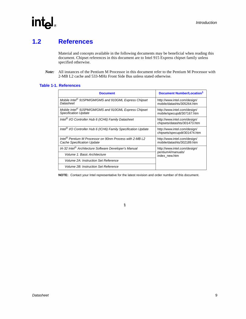
NOTE: Contact your Intel representative for the latest revision and order number of this document.
§
Table 1-1. References
Document Document Number/Location1
Mobile Intel® 915PM/GM/GMS and 910GML Express Chipset Datasheet
http://www.intel.com/design/mobile/datashts/305264.htm
Mobile Intel® 915PM/GM/GMS and 910GML Express Chipset Specification Update
http://www.intel.com/design/mobile/specupdt/307167.htm
Intel® I/O Controller Hub 6 (ICH6) Family Datasheet http://www.intel.com/design/chipsets/datashts/301473.htm
Intel® I/O Controller Hub 6 (ICH6) Family Specification Update http://www.intel.com/design/chipsets/specupdt/301474.htm
Intel® Pentium M Processor on 90nm Process with 2-MB L2 Cache Specification Update
http://www.intel.com/design/mobile/datashts/302189.htm
IA-32 Intel® Architecture Software Developer's Manual http://www.intel.com/design/pentium4/manuals/index_new.htmVolume 1: Basic Architecture
Volume 2A: Instruction Set Reference
Volume 2B: Instruction Set Reference

10 Datasheet
Introduction
Datasheet 11
Low Power Features
2 Low Power Features
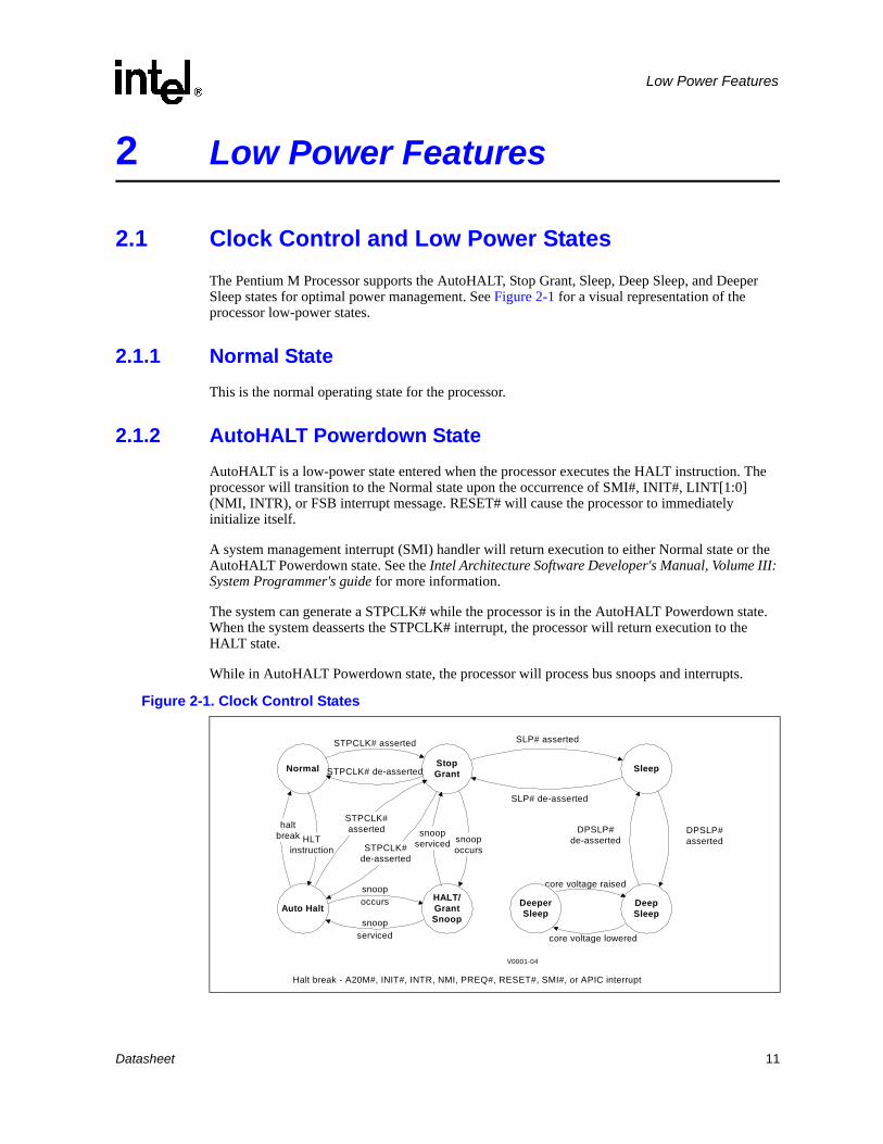
2.1 Clock Control and Low Power StatesThe Pentium M Processor supports the AutoHALT, Stop Grant, Sleep, Deep Sleep, and Deeper Sleep states for optimal power management. See Figure 2-1 for a visual representation of the processor low-power states.
2.1.1 Normal StateThis is the normal operating state for the processor.
2.1.2 AutoHALT Powerdown StateAutoHALT is a low-power state entered when the processor executes the HALT instruction. The processor will transition to the Normal state upon the occurrence of SMI#, INIT#, LINT[1:0] (NMI, INTR), or FSB interrupt message. RESET# will cause the processor to immediately initialize itself.
A system management interrupt (SMI) handler will return execution to either Normal state or the AutoHALT Powerdown state. See the Intel Architecture Software Developer's Manual, Volume III: System Programmer's guide for more information.
The system can generate a STPCLK# while the processor is in the AutoHALT Powerdown state. When the system deasserts the STPCLK# interrupt, the processor will return execution to the HALT state.
While in AutoHALT Powerdown state, the processor will process bus snoops and interrupts.
Figure 2-1. Clock Control States
snoopoccurs
StopGrantNormal Sleep
HALT/GrantSnoop
Auto Halt DeepSleep
STPCLK# asserted SLP# asserted
SLP# de-asserted
STPCLK# de-asserted
snoopserviced
HLTinstruction
snoopserviced snoop
occurs
DPSLP#de-asserted
DPSLP#asserted
STPCLK#asserted
STPCLK#de-asserted
haltbreak
V0001-04
core voltage raised
core voltage lowered
Halt break - A20M#, INIT#, INTR, NMI, PREQ#, RESET#, SMI#, or APIC interrupt
DeeperSleep
12 Datasheet
Low Power Features
2.1.3 Stop-Grant StateWhen the STPCLK# pin is asserted, the Stop-Grant state of the processor is entered 20 bus clocks after the response phase of the processor-issued Stop Grant Acknowledge special bus cycle.
Since the AGTL+ signal pins receive power from the FSB, these pins should not be driven (allowing the level to return to VCCP) for minimum power drawn by the termination resistors in this state. In addition, all other input pins on the FSB should be driven to the inactive state.
RESET# will cause the processor to immediately initialize itself, but the processor will stay in Stop-Grant state. A transition back to the Normal state will occur with the de-assertion of the STPCLK# signal. When re-entering the Stop-Grant state from the Sleep state, STPCLK# should be deasserted ten or more bus clocks after the de-assertion of SLP#.
A transition to the HALT/Grant Snoop state will occur when the processor detects a snoop on the FSB (see Section 2.1.4). A transition to the Sleep state (see Section 2.1.5) will occur with the assertion of the SLP# signal.
While in the Stop-Grant State, SMI#, INIT# and LINT[1:0] will be latched by the processor, and only serviced when the processor returns to the Normal State. Only one occurrence of each event will be recognized upon return to the Normal state.
While in Stop-Grant state, the processor will process snoops on the FSB and it will latch interrupts delivered on the FSB.
The PBE# signal can be driven when the processor is in Stop-Grant state. PBE# will be asserted if there is any pending interrupt latched within the processor. Pending interrupts that are blocked by the EFLAGS.IF bit being clear will still cause assertion of PBE#. Assertion of PBE# indicates to system logic that it should return the processor to the Normal state.
2.1.4 HALT/Grant Snoop StateThe processor will respond to snoop or interrupt transactions on the FSB while in Stop-Grant state or in AutoHALT Power Down state. During a snoop or interrupt transaction, the processor enters the HALT/Grant Snoop state. The processor will stay in this state until the snoop on the FSB has been serviced (whether by the processor or another agent on the FSB) or the interrupt has been latched. After the snoop is serviced or the interrupt is latched, the processor will return to the Stop-Grant state or AutoHALT Power Down state, as appropriate.
2.1.5 Sleep StateThe Sleep state is a low power state in which the processor maintains its context, maintains the phase-locked loop (PLL), and has stopped all internal clocks. The Sleep state can only be entered from Stop-Grant state. Once in the Stop-Grant state, the processor will enter the Sleep state upon the assertion of the SLP# signal. The SLP# pin should only be asserted when the processor is in the Stop Grant state. SLP# assertions while the processor is not in the Stop-Grant state is out of specification and may result in unapproved operation.
Snoop events that occur while in Sleep State or during a transition into or out of Sleep state will cause unpredictable behavior.
Datasheet 13
Low Power Features
In the Sleep state, the processor is incapable of responding to snoop transactions or latching interrupt signals. No transitions or assertions of signals (with the exception of SLP#, DPSLP# or RESET#) are allowed on the FSB while the processor is in Sleep state. Any transition on an input signal before the processor has returned to Stop-Grant state will result in unpredictable behavior.
If RESET# is driven active while the processor is in the Sleep state, and held active as specified in the RESET# pin specification, then the processor will reset itself, ignoring the transition through Stop-Grant State. If RESET# is driven active while the processor is in the Sleep State, the SLP# and STPCLK# signals should be deasserted immediately after RESET# is asserted to ensure the processor correctly executes the Reset sequence.
While in the Sleep state, the processor is capable of entering an even lower power state, the Deep Sleep state by asserting the DPSLP# pin. (See Section 2.1.6.) While the processor is in the Sleep state, the SLP# pin must be deasserted if another asynchronous FSB event needs to occur.
2.1.6 Deep Sleep StateDeep Sleep state is a very low power state the processor can enter while maintaining context. Deep Sleep state is entered by asserting the DPSLP# pin while in the Sleep state. BCLK may be stopped during the Deep Sleep state for additional platform level power savings. BCLK stop/restart timings on Intel® 915PM/GM and Intel® 915GMS/ICH6-M Express chipset-based platforms with the CK410/CK410M clock chip are as follows:
• Deep Sleep entry - DPSLP# and CPU_STP# are asserted simultaneously. CK410/CK410M will stop/tristate BCLK within 2 BCLKs +/- a few nanoseconds.
• Deep Sleep exit - DPSLP# and CPU_STP# are deasserted simultaneously. CK410/CK410M will drive BCLK to differential DC levels within 2 ~3 ns and starts toggling BCLK 2~6 BCLK periods later.
To re-enter the Sleep state, the DPSLP# pin must be deasserted. BCLK can be re-started after DPSLP# de-assertion as described above. A period of 30 microseconds (to allow for PLL stabilization) must occur before the processor can be considered to be in the Sleep state. Once in the Sleep state, the SLP# pin must be deasserted to re-enter the Stop-Grant state.
While in Deep Sleep state, the processor is incapable of responding to snoop transactions or latching interrupt signals. No transitions of signals are allowed on the FSB while the processor is in Deep Sleep state. Any transition on an input signal before the processor has returned to Stop-Grant state will result in unpredictable behavior.
When the processor is in Deep Sleep state, it will not respond to interrupts or snoop transactions.
2.1.7 Deeper Sleep StateThe Deeper Sleep State is the lowest state power the processor can enter. This state is functionally identical to the Deep Sleep state but at a lower core voltage. The control signals to the voltage regulator to initiate a transition to the Deeper Sleep state are provided on the platform.
14 Datasheet
Low Power Features
2.2 Enhanced Intel SpeedStep® Technology
The Pentium M Processor features Enhanced Intel SpeedStep Technology. Unlike previous implementations of Intel SpeedStep Technology, this technology enables the processor to switch between multiple frequency and voltage points instead of two. This will enable superior performance with optimal power savings. Switching between states is software controlled unlike previous implementations where the GHI# pin is used to toggle between two states.
Following are the key features of Enhanced Intel SpeedStep Technology:
• Multiple voltage/frequency operating points provide optimal performance at the lowest power.
• Voltage/Frequency selection is software controlled by writing to processor MSR’s (Model Specific Registers) thus eliminating chipset dependency.
— If the target frequency is higher than the current frequency, Vcc is ramped up by placing a new value on the VID pins and the PLL then locks to the new frequency.
— If the target frequency is lower than the current frequency, the PLL locks to the new frequency and the Vcc is changed through the VID pin mechanism.
— Software transitions are accepted at any time. If a previous transition is in progress, the new transition is deferred until its completion.
• The processor controls voltage ramp rates internally to ensure glitch free transitions.
• Low transition latency and large number of transitions possible per second.
— Processor core (including L2 cache) is unavailable for up to 10 µs during the frequency transition
— The bus protocol (BNR# mechanism) is used to block snooping
• No bus master arbiter disable required prior to transition and no processor cache flush necessary.
• Improved Intel® Thermal Monitor mode.
— When the on-die thermal sensor indicates that the die temperature is too high, the processor can automatically perform a transition to a lower frequency/voltage specified in a software programmable MSR.
— The processor waits for a fixed time period. If the die temperature is down to acceptable levels, an up transition to the previous frequency/voltage point occurs.
— An interrupt is generated for the up and down Intel Thermal Monitor transitions enabling better system level thermal management.

Datasheet 15
Low Power Features
2.3 FSB Low Power Enhancements
The Pentium M Processor incorporates the following FSB low power enhancements:
• Dynamic FSB Power Down
• BPRI# control for address and control input buffers
• Dynamic On Die Termination disabling
• Low VCCP (I/O termination voltage)
The Pentium M Processor incorporates the DPWR# signal that controls the data bus input buffers on the processor. The DPWR# signal disables the buffers when not used and activates them only when data bus activity occurs, resulting in significant power savings with no performance impact. BPRI# control also allows the processor address and control input buffers to be turned off when the BPRI# signal is inactive. The On Die Termination on the processor FSB buffers is disabled when the signals are driven low, resulting in additional power savings. The low I/O termination voltage is on a dedicated voltage plane independent of the core voltage, enabling low I/O switching power at all times.
2.4 Processor Power Status Indicator (PSI#) Signal
The Pentium M Processor incorporates the PSI# signal that is asserted when the processor is in a low power (Deep Sleep or Deeper Sleep) state. This signal is asserted upon Deep Sleep entry and deasserted upon exit. PSI# can be used to improve the light load efficiency of the voltage regulator, resulting in platform power savings and extended battery life. PSI# can also be used to simplify voltage regulator designs since it removes the need for integrated 100 µs timers required to mask the PWRGOOD signal during Deeper Sleep transitions. It also helps loosen PWRGOOD monitoring requirements in the Deeper Sleep state
§

16 Datasheet
Low Power Features
Datasheet 17
Electrical Specifications
3 Electrical Specifications
3.1 Power and Ground PinsFor clean, on-chip power distribution, the Pentium M Processor will have a large number of VCC (power) and VSS (ground) inputs. All power pins must be connected to VCC power planes while all VSS pins must be connected to system ground planes. Use of multiple power and ground planes is recommended to reduce I*R drop. The processor VCC pins must be supplied the voltage determined by the VID (Voltage ID) pins.
3.2 FSB Clock (BCLK[1:0]) and Processor ClockingBCLK[1:0] directly controls the FSB interface speed as well as the core frequency of the processor. As in previous generation processors, the Pentium M Processor core frequency is a multiple of the BCLK[1:0] frequency. The Pentium M Processor uses a differential clocking implementation.
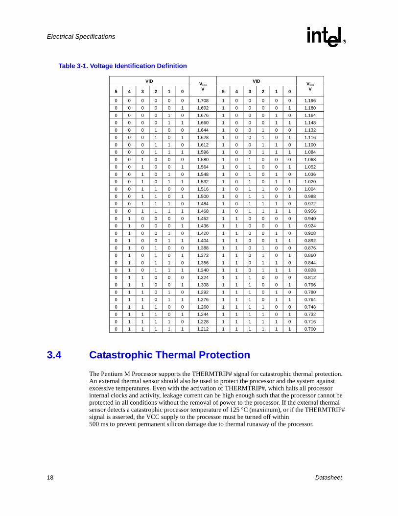
3.3 Voltage IdentificationThe Pentium M Processor uses six voltage identification pins, VID[5:0], to support automatic selection of power supply voltages. The VID pins for the Pentium M Processor are CMOS outputs driven by the processor VID circuitry. Table 3-1 specifies the voltage level corresponding to the state of VID[5:0]. A “1” in this refers to a high-voltage level and a “0” refers to low-voltage level.
18 Datasheet
Electrical Specifications
Table 3-1. Voltage Identification Definition
3.4 Catastrophic Thermal ProtectionThe Pentium M Processor supports the THERMTRIP# signal for catastrophic thermal protection. An external thermal sensor should also be used to protect the processor and the system against excessive temperatures. Even with the activation of THERMTRIP#, which halts all processor internal clocks and activity, leakage current can be high enough such that the processor cannot be protected in all conditions without the removal of power to the processor. If the external thermal sensor detects a catastrophic processor temperature of 125 °C (maximum), or if the THERMTRIP# signal is asserted, the VCC supply to the processor must be turned off within 500 ms to prevent permanent silicon damage due to thermal runaway of the processor.
VID VID
5 4 3 2 1 0 VCC V 5 4 3 2 1 0
VCC V
0 0 0 0 0 0 1.708 1 0 0 0 0 0 1.196 0 0 0 0 0 1 1.692 1 0 0 0 0 1 1.180 0 0 0 0 1 0 1.676 1 0 0 0 1 0 1.164 0 0 0 0 1 1 1.660 1 0 0 0 1 1 1.148 0 0 0 1 0 0 1.644 1 0 0 1 0 0 1.132 0 0 0 1 0 1 1.628 1 0 0 1 0 1 1.116 0 0 0 1 1 0 1.612 1 0 0 1 1 0 1.100 0 0 0 1 1 1 1.596 1 0 0 1 1 1 1.084 0 0 1 0 0 0 1.580 1 0 1 0 0 0 1.068 0 0 1 0 0 1 1.564 1 0 1 0 0 1 1.052 0 0 1 0 1 0 1.548 1 0 1 0 1 0 1.036 0 0 1 0 1 1 1.532 1 0 1 0 1 1 1.020 0 0 1 1 0 0 1.516 1 0 1 1 0 0 1.004 0 0 1 1 0 1 1.500 1 0 1 1 0 1 0.988 0 0 1 1 1 0 1.484 1 0 1 1 1 0 0.972 0 0 1 1 1 1 1.468 1 0 1 1 1 1 0.956 0 1 0 0 0 0 1.452 1 1 0 0 0 0 0.940 0 1 0 0 0 1 1.436 1 1 0 0 0 1 0.924 0 1 0 0 1 0 1.420 1 1 0 0 1 0 0.908 0 1 0 0 1 1 1.404 1 1 0 0 1 1 0.892 0 1 0 1 0 0 1.388 1 1 0 1 0 0 0.876 0 1 0 1 0 1 1.372 1 1 0 1 0 1 0.860 0 1 0 1 1 0 1.356 1 1 0 1 1 0 0.844 0 1 0 1 1 1 1.340 1 1 0 1 1 1 0.828 0 1 1 0 0 0 1.324 1 1 1 0 0 0 0.812 0 1 1 0 0 1 1.308 1 1 1 0 0 1 0.796 0 1 1 0 1 0 1.292 1 1 1 0 1 0 0.780 0 1 1 0 1 1 1.276 1 1 1 0 1 1 0.764 0 1 1 1 0 0 1.260 1 1 1 1 0 0 0.748 0 1 1 1 0 1 1.244 1 1 1 1 0 1 0.732 0 1 1 1 1 0 1.228 1 1 1 1 1 0 0.716 0 1 1 1 1 1 1.212 1 1 1 1 1 1 0.700
Datasheet 19
Electrical Specifications
3.5 Signal Terminations and Unused PinsAll RSVD (RESERVED) pins must remain unconnected. Connection of these pins to VCC, VSS, or to any other signal (including each other) can result in component malfunction or incompatibility with future Pentium M Processors. See Section 4.1 for a pin listing of the processor and the location of all RSVD pins.
For reliable operation, always connect unused inputs or bidirectional signals to an appropriate signal level. Unused active low AGTL+ inputs may be left as no connects if AGTL+ termination is provided on the processor silicon. Unused active high inputs should be connected through a resistor to ground (VSS). Unused outputs can be left unconnected.
The TEST1 and TEST2 pins must have a stuffing option connection to VSS separately via 1 kΩ, pull-down resistors.
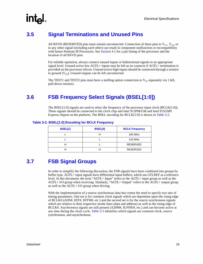
3.6 FSB Frequency Select Signals (BSEL[1:0])
The BSEL[1:0] signals are used to select the frequency of the processor input clock (BCLK[1:0]). These signals should be connected to the clock chip and Intel 915PM/GM and Intel 915GMS Express chipset on the platform. The BSEL encoding for BCLK[1:0] is shown in Table 3-2.
3.7 FSB Signal GroupsIn order to simplify the following discussion, the FSB signals have been combined into groups by buffer type. AGTL+ input signals have differential input buffers, which use GTLREF as a reference level. In this document, the term “AGTL+ Input” refers to the AGTL+ input group as well as the AGTL+ I/O group when receiving. Similarly, “AGTL+ Output” refers to the AGTL+ output group as well as the AGTL+ I/O group when driving.
With the implementation of a source synchronous data bus comes the need to specify two sets of timing parameters. One set is for common clock signals which are dependant upon the rising edge of BCLK0 (ADS#, HIT#, HITM#, etc.) and the second set is for the source synchronous signals which are relative to their respective strobe lines (data and address) as well as the rising edge of BCLK0. Asychronous signals are still present (A20M#, IGNNE#, etc.) and can become active at any time during the clock cycle. Table 3-3 identifies which signals are common clock, source synchronous, and asynchronous.
Table 3-2. BSEL[1:0] Encoding for BCLK Frequency
BSEL[1] BSEL[0] BCLK Frequency
L H 100 MHz
L L 133 MHz
H L RESERVED
H H RESERVED

20 Datasheet
Electrical Specifications
NOTES:1. Refer to Table 4-5 for signal descriptions and termination requirements.2. In processor systems where there is no debug port implemented on the system board, these signals are used
to support a debug port interposer. In systems with the debug port implemented on the system board, these signals are no connects.
3. BPM[2:0]# and PRDY# are AGTL+ output only signals.
3.8 CMOS SignalsCMOS input signals are shown in Table 3-3. Legacy output FERR#, IERR# and other non-AGTL+ signals (THERMTRIP# and PROCHOT#) utilize Open Drain output buffers. These signals do not have setup or hold time specifications in relation to BCLK[1:0]. However, all of the CMOS signals are required to be asserted for at least three BCLKs in order for the processor to recognize them. See Section 3.10 for the DC and AC specifications for the CMOS signal groups.
Table 3-3. FSB Pin Groups
Signal Group Type Signals1
AGTL+ Common Clock Input Synchronous to BCLK[1:0]
BPRI#, DEFER#, DPWR#, PREQ#, RESET#, RS[2:0]#, TRDY#
AGTL+ Common Clock I/O Synchronous to BCLK[1:0]
ADS#, BNR#, BPM[3:0]#3, BR0#, DBSY#, DRDY#, HIT#, HITM#, LOCK#, PRDY#3
AGTL+ Source Synchronous I/O Synchronous to assoc. strobe
AGTL+ Strobes Synchronous to BCLK[1:0]
ADSTB[1:0]#, DSTBP[3:0]#, DSTBN[3:0]#
CMOS Input Asynchronous A20M#, DPSLP#, IGNNE#, INIT#, LINT0/INTR, LINT1/NMI, PWRGOOD, SMI#, SLP#, STPCLK#
Open Drain Output Asynchronous FERR#, IERR#, PROCHOT#, THERMTRIP#
CMOS Output Asynchronous PSI#, VID[5:0], BSEL[1:0]
CMOS Input Synchronous to TCK
TCK, TDI, TMS, TRST#
Open Drain Output Synchronous to TCK
TDO
FSB Clock Clock BCLK[1:0], ITP_CLK[1:0]2
Power/Other COMP[3:0], DBR#2, GTLREF, RSVD, TEST2, TEST1, THERMDA, THERMDC, VCC, VCCA, VCCP, VCCQ[1:0], VCC_SENSE, VSS, VSS_SENSE
Signals Associated Strobe
REQ[4:0]#, A[16:3]# ADSTB[0]#
A[31:17]# ADSTB[1]#
D[15:0]#, DINV0# DSTBP0#, DSTBN0#
D[31:16]#, DINV1# DSTBP1#, DSTBN1#
D[47:32]#, DINV2# DSTBP2#, DSTBN2#
D[63:48]#, DINV3# DSTBP3#, DSTBN3#
Datasheet 21
Electrical Specifications
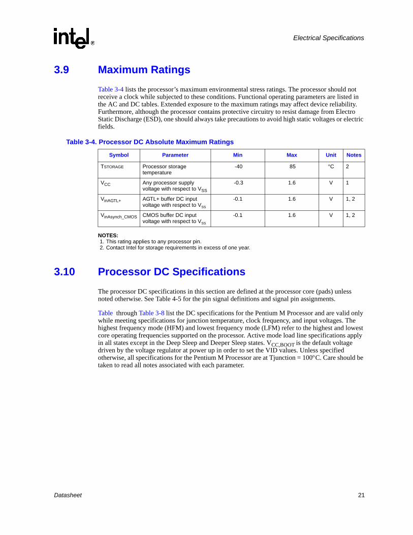
3.9 Maximum RatingsTable 3-4 lists the processor’s maximum environmental stress ratings. The processor should not receive a clock while subjected to these conditions. Functional operating parameters are listed in the AC and DC tables. Extended exposure to the maximum ratings may affect device reliability. Furthermore, although the processor contains protective circuitry to resist damage from Electro Static Discharge (ESD), one should always take precautions to avoid high static voltages or electric fields.
NOTES:1. This rating applies to any processor pin.2. Contact Intel for storage requirements in excess of one year.
3.10 Processor DC SpecificationsThe processor DC specifications in this section are defined at the processor core (pads) unless noted otherwise. See Table 4-5 for the pin signal definitions and signal pin assignments.
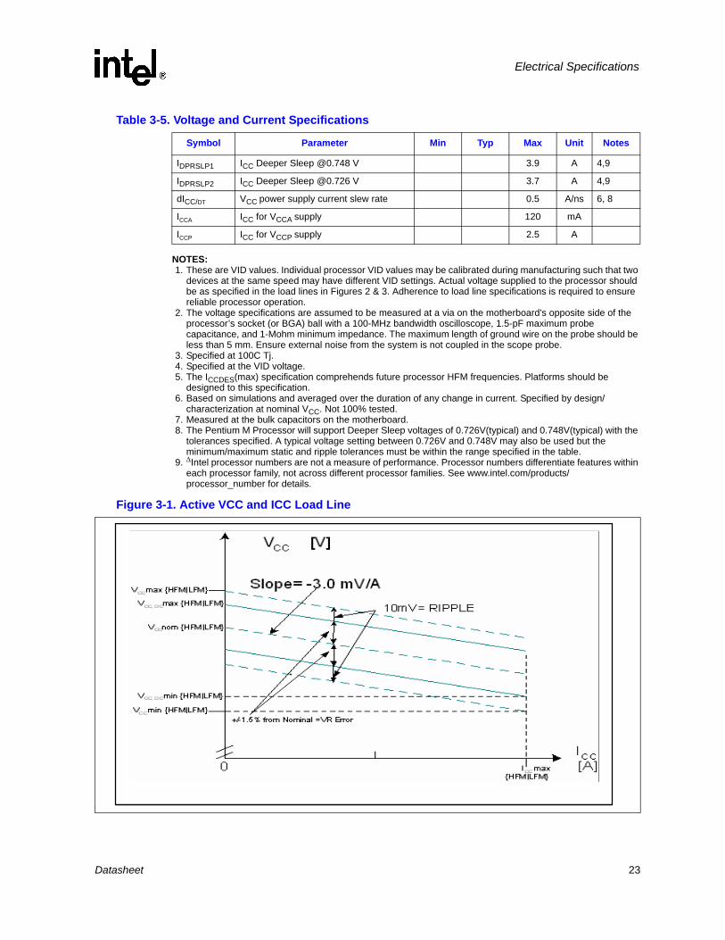
Table through Table 3-8 list the DC specifications for the Pentium M Processor and are valid only while meeting specifications for junction temperature, clock frequency, and input voltages. The highest frequency mode (HFM) and lowest frequency mode (LFM) refer to the highest and lowest core operating frequencies supported on the processor. Active mode load line specifications apply in all states except in the Deep Sleep and Deeper Sleep states. VCC,BOOT is the default voltage driven by the voltage regulator at power up in order to set the VID values. Unless specified otherwise, all specifications for the Pentium M Processor are at Tjunction = 100°C. Care should be taken to read all notes associated with each parameter.
Table 3-4. Processor DC Absolute Maximum Ratings
Symbol Parameter Min Max Unit Notes
TSTORAGE Processor storage temperature
-40 85 °C 2
VCC Any processor supply voltage with respect to VSS
-0.3 1.6 V 1
VinAGTL+ AGTL+ buffer DC input voltage with respect to VSS
-0.1 1.6 V 1, 2
VinAsynch_CMOS CMOS buffer DC input voltage with respect to VSS
-0.1 1.6 V 1, 2
22 Datasheet
Electrical Specifications
Table 3-5. Voltage and Current Specifications
Symbol Parameter Min Typ Max Unit Notes
VCCHFM1 Vcc at Highest Frequency Mode (HFM) for Intel® Pentium® M Processors 730, 740, 750, 760
1.260 1.356 V 1, 2
VCCHFM2 Vcc at Highest Frequency Mode (HFM) for the Pentium M Processor 770
1.260 1.372 V 1, 2
VCCHFM3 Vcc at Highest Frequency Mode (HFM) for the Pentium M Processor 780
1.260 1.404 V 1, 2
VCCLFM Vcc at Lowest Frequency Mode (LFM) 0.988 V 1, 2
VCC,BOOT Default VCC Voltage for initial power up 1.14 1.20 1.26 V 2
VCCP AGTL+ Termination Voltage 0.997 1.05 1.102 V 2
VCCA PLL supply voltage 1.425 1.5 1.575 V 2
VCCDPRSLP,RP1
Ripple Deeper Sleep voltage 0.689 0.748 0.807 V 2,9
VCCDPRSLP,ST1
Static Deeper Sleep voltage 0.699 0.748 0.797 V 2,9
VCCDPRSLP,RP2
Ripple Deeper Sleep voltage 0.669 0.726 0.783 V 2,9
VCCDPRSLP,ST2
Static Deeper Sleep voltage 0.679 0.726 0.773 V 2,9
ICCDES ICC for Pentium M ProcessorsRecommended Design Target
27 A 5
ICC Icc for Pentium M Processors A 3,4
Processor Number
Core Frequency/Voltage
780 2.26 GHz and HFM Vcc 26
770 2.13 GHz and HFM Vcc 26
760 2.0 GHz and HFM Vcc 26
750 1.86 GHz and HFM Vcc 26
740 1.73 GHz and HFM Vcc 26
730 1.6 GHz and HFM Vcc 26
Not Applicable
800 MHz and LFM Vcc 12.2
IAH,ISGNT
ICC Auto-Halt & Stop-Grant A 3,4
LFM 9.2
HFM 23.1
ISLP ICC Sleep A 3,4
LFM 9.1
HFM 22.7
IDSLP ICC Deep Sleep A 3,4
LFM 8.9
HFM 22.1
Datasheet 23
Electrical Specifications
NOTES:1. These are VID values. Individual processor VID values may be calibrated during manufacturing such that two
devices at the same speed may have different VID settings. Actual voltage supplied to the processor should be as specified in the load lines in Figures 2 & 3. Adherence to load line specifications is required to ensure reliable processor operation.
2. The voltage specifications are assumed to be measured at a via on the motherboard’s opposite side of the processor’s socket (or BGA) ball with a 100-MHz bandwidth oscilloscope, 1.5-pF maximum probe capacitance, and 1-Mohm minimum impedance. The maximum length of ground wire on the probe should be less than 5 mm. Ensure external noise from the system is not coupled in the scope probe.
3. Specified at 100C Tj. 4. Specified at the VID voltage.5. The ICCDES(max) specification comprehends future processor HFM frequencies. Platforms should be
designed to this specification. 6. Based on simulations and averaged over the duration of any change in current. Specified by design/
characterization at nominal VCC. Not 100% tested.7. Measured at the bulk capacitors on the motherboard.8. The Pentium M Processor will support Deeper Sleep voltages of 0.726V(typical) and 0.748V(typical) with the
tolerances specified. A typical voltage setting between 0.726V and 0.748V may also be used but the minimum/maximum static and ripple tolerances must be within the range specified in the table.
9. ∆Intel processor numbers are not a measure of performance. Processor numbers differentiate features within each processor family, not across different processor families. See www.intel.com/products/processor_number for details.
IDPRSLP1 ICC Deeper Sleep @0.748 V 3.9 A 4,9
IDPRSLP2 ICC Deeper Sleep @0.726 V 3.7 A 4,9
dICC/DT VCC power supply current slew rate 0.5 A/ns 6, 8
ICCA ICC for VCCA supply 120 mA
ICCP ICC for VCCP supply 2.5 A
Table 3-5. Voltage and Current Specifications
Symbol Parameter Min Typ Max Unit Notes
Figure 3-1. Active VCC and ICC Load Line
24 Datasheet
Electrical Specifications
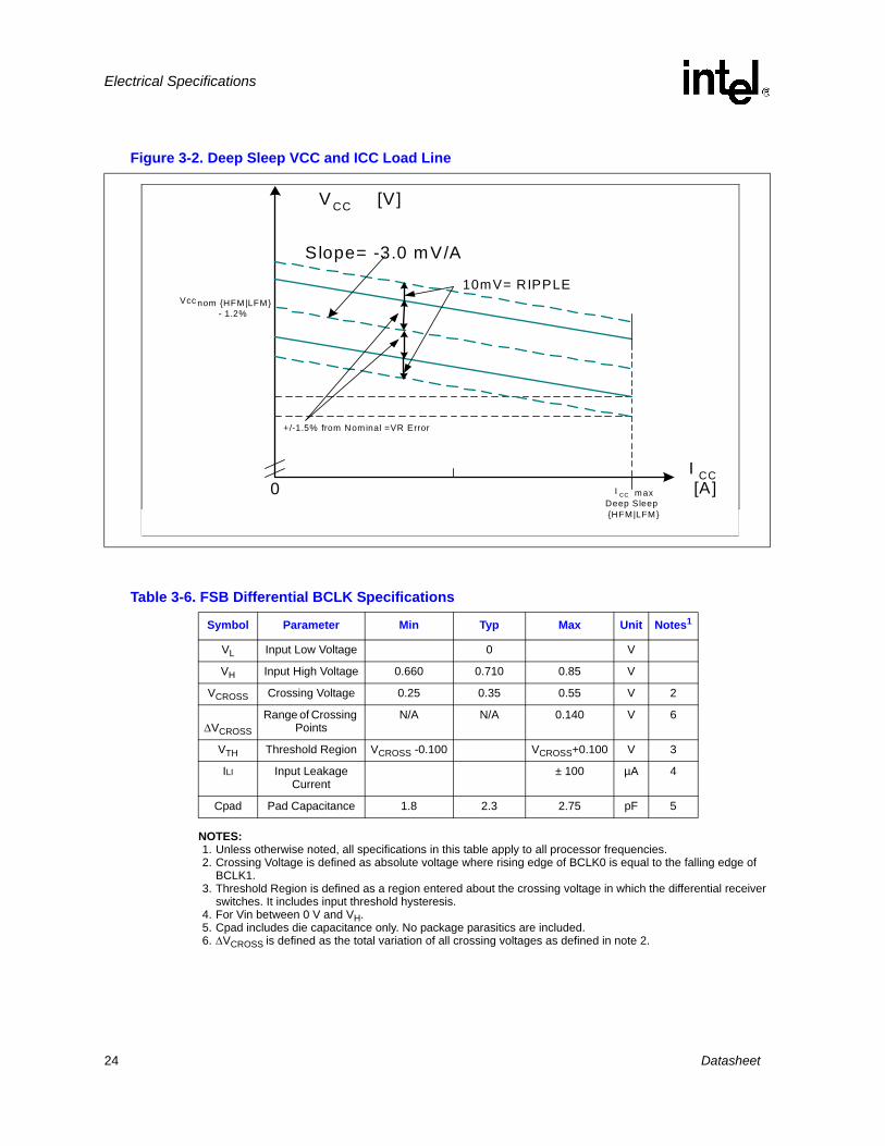
NOTES:1. Unless otherwise noted, all specifications in this table apply to all processor frequencies.2. Crossing Voltage is defined as absolute voltage where rising edge of BCLK0 is equal to the falling edge of
BCLK1. 3. Threshold Region is defined as a region entered about the crossing voltage in which the differential receiver
switches. It includes input threshold hysteresis.4. For Vin between 0 V and VH.5. Cpad includes die capacitance only. No package parasitics are included.6. ∆VCROSS is defined as the total variation of all crossing voltages as defined in note 2.
Figure 3-2. Deep Sleep VCC and ICC Load Line
I CC max
HFM|LFM
V CC [V]
Slope= -3.0 mV/A
Vcc nom HFM|LFM- 1.2%
+/-1.5% from Nominal =VR Error
10mV= RIPPLE
I CC[A]0
Deep Sleep
Table 3-6. FSB Differential BCLK Specifications
Symbol Parameter Min Typ Max Unit Notes1
VL Input Low Voltage 0 V
VH Input High Voltage 0.660 0.710 0.85 V
VCROSS Crossing Voltage 0.25 0.35 0.55 V 2
∆VCROSS
Range of Crossing Points
N/A N/A 0.140 V 6
VTH Threshold Region VCROSS -0.100 VCROSS+0.100 V 3
ILI Input Leakage Current
± 100 µA 4
Cpad Pad Capacitance 1.8 2.3 2.75 pF 5
Datasheet 25
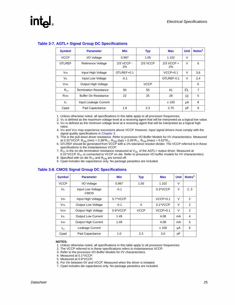
Electrical Specifications
1. Unless otherwise noted, all specifications in this table apply to all processor frequencies.2. VIL is defined as the maximum voltage level at a receiving agent that will be interpreted as a logical low value.3. VIH is defined as the minimum voltage level at a receiving agent that will be interpreted as a logical high
value.4. VIH and VOH may experience excursions above VCCP. However, input signal drivers must comply with the
signal quality specifications in Chapter 3.5. This is the pull down driver resistance. Refer to processor I/O Buffer Models for I/V characteristics. Measured
at 0.31*VCCP. RON (min) = 0.38*RTT, RON (typ) = 0.45*RTT, RON (max) = 0.52*RTT.6. GTLREF should be generated from VCCP with a 1% tolerance resistor divider. The VCCP referred to in these
specifications is the instantaneous VCCP.7. RTT is the on-die termination resistance measured at VOL of the AGTL+ output driver. Measured at
0.31*VCCP. RTT is connected to VCCP on die. Refer to processor I/O buffer models for I/V characteristics.8. Specified with on die RTT and RON are turned off.9. Cpad includes die capacitance only. No package parasitics are included.
NOTES:1. Unless otherwise noted, all specifications in this table apply to all processor frequencies.2. The VCCP referred to in these specifications refers to instantaneous VCCP.3. Refer to the processor I/O Buffer Models for I/V characteristics.4. Measured at 0.1*VCCP. 5. Measured at 0.9*VCCP. 6. For Vin between 0V and VCCP. Measured when the driver is tristated.7. Cpad includes die capacitance only. No package parasitics are included.
Table 3-7. AGTL+ Signal Group DC Specifications
Symbol Parameter Min Typ Max Unit Notes1
VCCP I/O Voltage 0.997 1.05 1.102 V
GTLREF Reference Voltage 2/3 VCCP - 2%
2/3 VCCP 2/3 VCCP + 2%
V 6
VIH Input High Voltage GTLREF+0.1 VCCP+0.1 V 3,6
VIL Input Low Voltage -0.1 GTLREF-0.1 V 2,4
VOH Output High Voltage VCCP 6
RTT Termination Resistance 50 55 61 Ω, 7
RON Buffer On Resistance 22 25 28 Ω 5
ILI Input Leakage Current ± 100 µA 8
Cpad Pad Capacitance 1.8 2.3 2.75 pF 9
Table 3-8. CMOS Signal Group DC Specifications
Symbol Parameter Min Typ Max Unit Notes1
VCCP I/O Voltage 0.997 1.05 1.102 V
VIL Input Low VoltageCMOS
-0.1 0.3*VCCP V 2, 3
VIH Input High Voltage 0.7*VCCP VCCP+0.1 V 2
VOL Output Low Voltage -0.1 0 0.1*VCCP V 2
VOH Output High Voltage 0.9*VCCP VCCP VCCP+0.1 V 2
IOL Output Low Current 1.49 4.08 mA 4
IOH Output High Current 1.49 4.08 mA 5
ILI Leakage Current ± 100 µA 6
Cpad Pad Capacitance 1.0 2.3 3.0 pF
26 Datasheet
Electrical Specifications
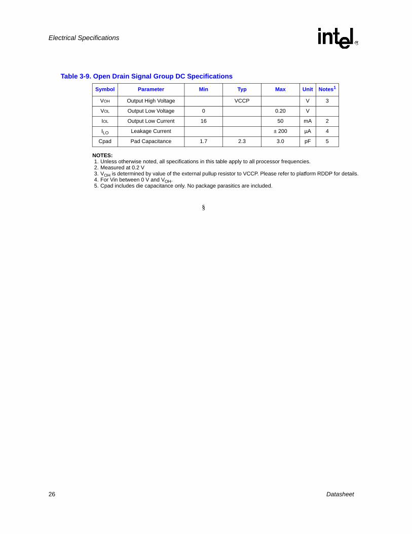
.
NOTES:1. Unless otherwise noted, all specifications in this table apply to all processor frequencies.2. Measured at 0.2 V3. VOH is determined by value of the external pullup resistor to VCCP. Please refer to platform RDDP for details.4. For Vin between 0 V and VOH.5. Cpad includes die capacitance only. No package parasitics are included.
§
Table 3-9. Open Drain Signal Group DC Specifications
Symbol Parameter Min Typ Max Unit Notes1
VOH Output High Voltage VCCP V 3
VOL Output Low Voltage 0 0.20 V
IOL Output Low Current 16 50 mA 2
ILO Leakage Current ± 200 µA 4
Cpad Pad Capacitance 1.7 2.3 3.0 pF 5
Datasheet 27
Package Mechanical Specifications and Pin Information
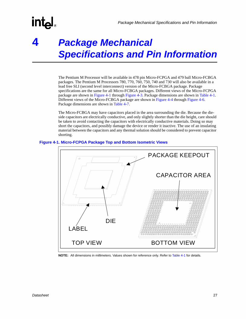
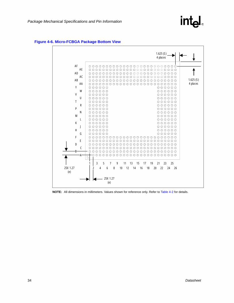
4 Package Mechanical Specifications and Pin Information
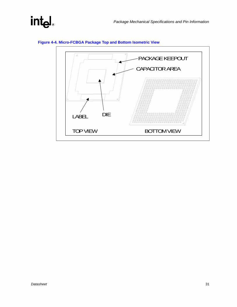
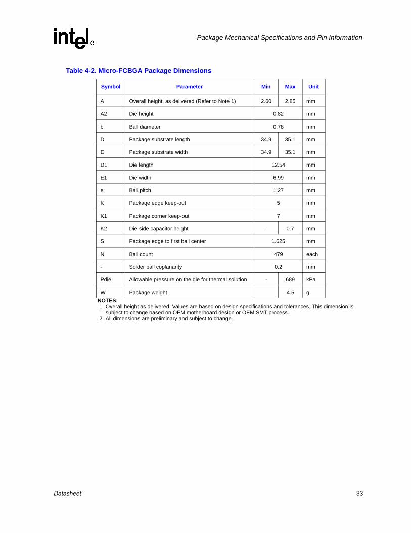
The Pentium M Processor will be available in 478 pin Micro-FCPGA and 479 ball Micro-FCBGA packages. The Pentium M Processors 780, 770, 760, 750, 740 and 730 will also be available in a lead free SLI (second level interconnect) version of the Micro-FCBGA package. Package specifications are the same for all Micro-FCBGA packages. Different views of the Micro-FCPGA package are shown in Figure 4-1 through Figure 4-3. Package dimensions are shown in Table 4-1. Different views of the Micro-FCBGA package are shown in Figure 4-4 through Figure 4-6. Package dimensions are shown in Table 4-7.
The Micro-FCBGA may have capacitors placed in the area surrounding the die. Because the die-side capacitors are electrically conductive, and only slightly shorter than the die height, care should be taken to avoid contacting the capacitors with electrically conductive materials. Doing so may short the capacitors, and possibly damage the device or render it inactive. The use of an insulating material between the capacitors and any thermal solution should be considered to prevent capacitor shorting.
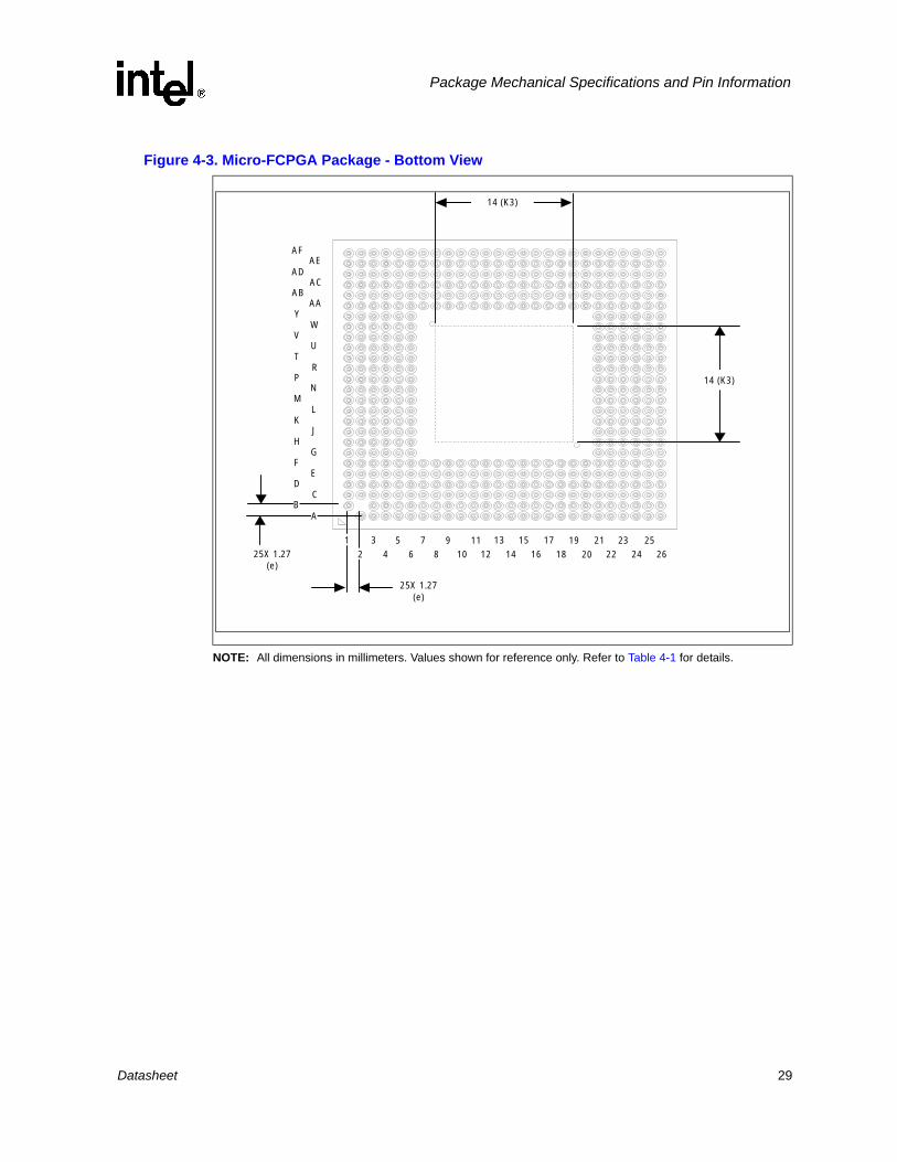
NOTE: All dimensions in millimeters. Values shown for reference only. Refer to Table 4-1 for details.
Figure 4-1. Micro-FCPGA Package Top and Bottom Isometric Views
TOP VIEW BOTTOM VIEW
LABEL
PACKAGE KEEPOUT
DIE
CAPACITOR AREA
28 Datasheet
Package Mechanical Specifications and Pin Information
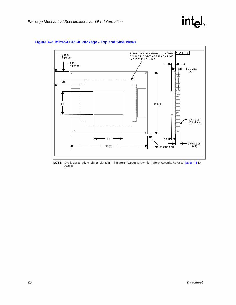
NOTE: Die is centered. All dimensions in millimeters. Values shown for reference only. Refer to Table 4-1 for details.
Figure 4-2. Micro-FCPGA Package - Top and Side Views
35 (E)
35 (D )
P IN A 1 C OR N ER
E 1
D 1
A 1 .25 M A X
(A 3)
Ø 0.32 (B )478 p laces
2 .03 ± 0.08(A 1)
A 2
S U B STR ATE K E EP O U T ZO N E D O N O T C O N TAC T P A C K AG E IN S ID E TH IS L IN E
7 (K 1) 8 p laces
5 (K) 4 p laces
0 .286
35 (E)
35 (D )
P IN A 1 C OR N ER
E 1
D 1
A 1 .25 M A X
(A 3)
Ø 0.32 (B )478 p laces
2 .03 ± 0.08(A 1)
A 2
S U B STR ATE K E EP O U T ZO N E D O N O T C O N TAC T P A C K AG E IN S ID E TH IS L IN E
7 (K 1) 8 p laces
5 (K) 4 p laces
0 .286 0 .286
Datasheet 29
Package Mechanical Specifications and Pin Information
NOTE: All dimensions in millimeters. Values shown for reference only. Refer to Table 4-1 for details.
Figure 4-3. Micro-FCPGA Package - Bottom View
1 2
34 6 8 10 12 14 16 18 20 22 24 26
5 7 9 11 13 15 17 19 21 23 25
A B
C E
D F
G H
J K
L M
N P
R T
U V
W Y
AA AB
AC AD
AE AF
25X 1.27 (e)
25X 1.27 (e)
14 (K3)
14 (K3)
30 Datasheet
Package Mechanical Specifications and Pin Information
1. Overall height with socket is based on design dimensions of the Micro-FCPGA package with no thermal solution attached. Values are based on design specifications and tolerances. This dimension is subject to change based on socket design, OEM motherboard design or OEM SMT process.
2. All dimensions are preliminary and subject to change.
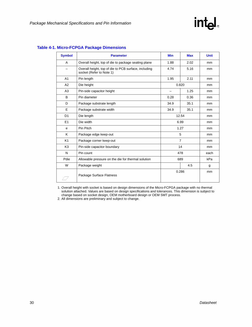
Table 4-1. Micro-FCPGA Package Dimensions
Symbol Parameter Min Max Unit
A Overall height, top of die to package seating plane 1.88 2.02 mm
– Overall height, top of die to PCB surface, including socket (Refer to Note 1)
4.74 5.16 mm
A1 Pin length 1.95 2.11 mm
A2 Die height 0.820 mm
A3 Pin-side capacitor height – 1.25 mm
B Pin diameter 0.28 0.36 mm
D Package substrate length 34.9 35.1 mm
E Package substrate width 34.9 35.1 mm
D1 Die length 12.54 mm
E1 Die width 6.99 mm
e Pin Pitch 1.27 mm
K Package edge keep-out 5 mm
K1 Package corner keep-out 7 mm
K3 Pin-side capacitor boundary 14 mm
N Pin count 478 each
Pdie Allowable pressure on the die for thermal solution 689 kPa
W Package weight 4.5 g
Package Surface Flatness0.286 mm
Datasheet 31
Package Mechanical Specifications and Pin Information
Figure 4-4. Micro-FCBGA Package Top and Bottom Isometric View
TOP VIEW BOTTOM VIEW
LABEL DIE
PACKAGE KEEPOUT
CAPACITOR AREA
32 Datasheet
Package Mechanical Specifications and Pin Information
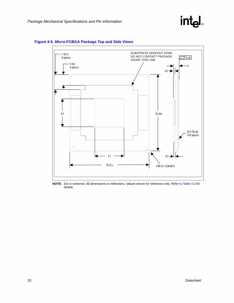
NOTE: Die is centered. All dimensions in millimeters. Values shown for reference only. Refer to Table 4-2 for details.
Figure 4-5. Micro-FCBGA Package Top and Side Views
35 (E)
35 (D)
PIN A1 CORNER
E1
D1
A
Ø 0.78 (b)479 places
K2
SUBSTRATE KEEPOUT ZONE DO NOT CONTACT PACKAGE INSIDE THIS LINE
7 (K1) 8 places
5 (K) 4 places
A2
0.20
Datasheet 33
Package Mechanical Specifications and Pin Information
NOTES:1. Overall height as delivered. Values are based on design specifications and tolerances. This dimension is
subject to change based on OEM motherboard design or OEM SMT process.2. All dimensions are preliminary and subject to change.
Table 4-2. Micro-FCBGA Package Dimensions
Symbol Parameter Min Max Unit
A Overall height, as delivered (Refer to Note 1) 2.60 2.85 mm
A2 Die height 0.82 mm
b Ball diameter 0.78 mm
D Package substrate length 34.9 35.1 mm
E Package substrate width 34.9 35.1 mm
D1 Die length 12.54 mm
E1 Die width 6.99 mm
e Ball pitch 1.27 mm
K Package edge keep-out 5 mm
K1 Package corner keep-out 7 mm
K2 Die-side capacitor height - 0.7 mm
S Package edge to first ball center 1.625 mm
N Ball count 479 each
- Solder ball coplanarity 0.2 mm
Pdie Allowable pressure on the die for thermal solution - 689 kPa
W Package weight 4.5 g
34 Datasheet
Package Mechanical Specifications and Pin Information
NOTE: All dimensions in millimeters. Values shown for reference only. Refer to Table 4-2 for details.
Figure 4-6. Micro-FCBGA Package Bottom View
1 2
34 6 8 10 12 14 16 18 20 22 24 26
5 7 9 11 13 15 17 19 21 23 25
A B
C E
D F
G H
J K
L M
N P
R T
U V
W Y
AA AB
AC AD
AE AF
25X 1.27 (e)
25X 1.27 (e)
1.625 (S)4 places
1.625 (S) 4 places
Datasheet 35
Package Mechanical Specifications and Pin Information
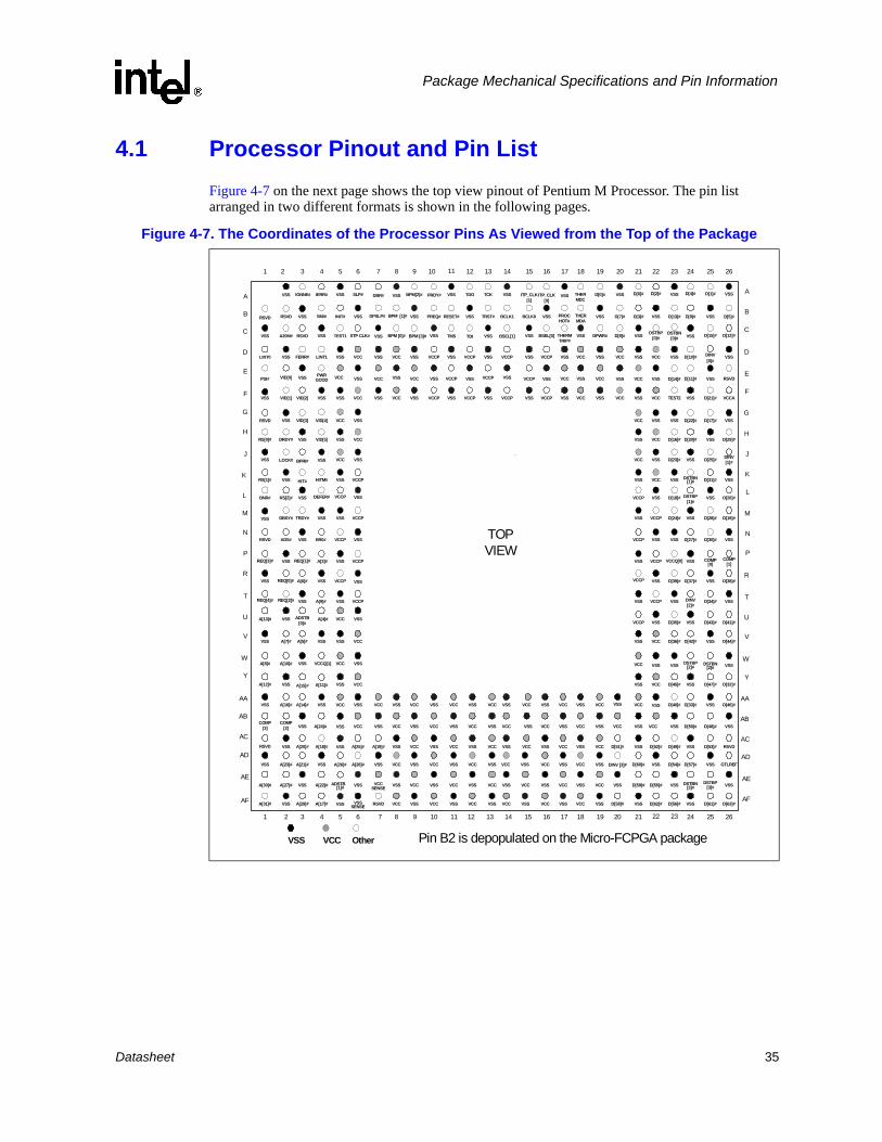
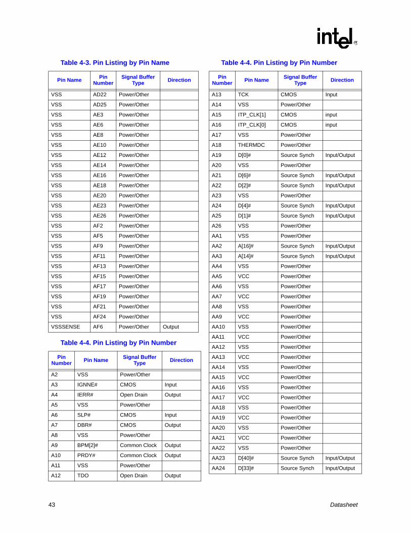
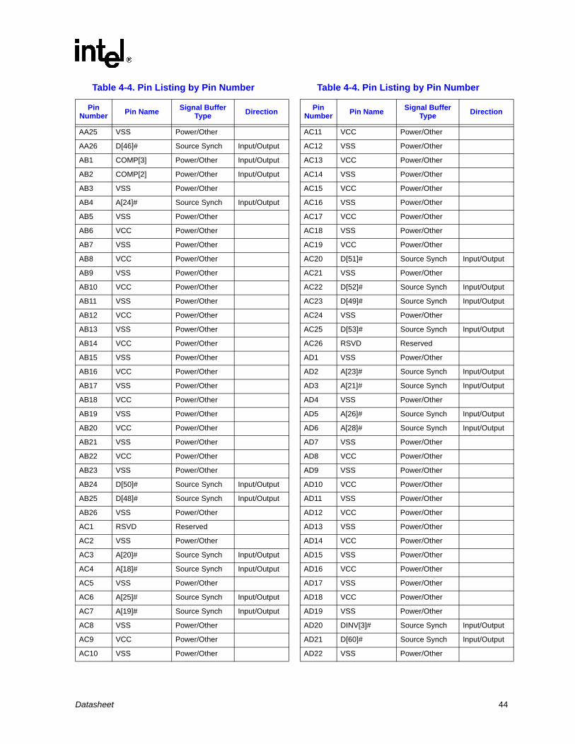
4.1 Processor Pinout and Pin ListFigure 4-7 on the next page shows the top view pinout of Pentium M Processor. The pin list arranged in two different formats is shown in the following pages.
Figure 4-7. The Coordinates of the Processor Pins As Viewed from the Top of the Package
1 2 3 4 5 6 7 8 9 10 11 12 13 14 15 16 17 18 19 20 21 22 23 24 25 26
IGNNE# IERR# VSS SLP# DBR# VSS BPM[2]# PRDY# VSS TDO TCK VSS ITP_CLK[1]
ITP_CLK[0]
VSS THERMDC
D[0]# VSS D[6]# D[2]# VSS D[4]# D[1]# VSS
VSS SMI# INIT# VSS DPSLP# BPM [1]# VSS PREQ# RESET# VSS TRST# BCLK1 BCLK0 VSS PROCHOT#
THERMDA
VSS D[7]# D[3]# VSS D[13]# D[9]# VSS D[5]#
VSS A20M# RSVD VSS TEST1 STP CLK# VSS BPM [0]# BPM [3]# VSS TMS TDI VSS BSEL[1] VSS BSEL[0] THERMTRIP#
VSS DPWR# D[8]# VSS DSTBP[0]#
DSTBN[0]# VSS D[15]# D[12]#
LINT0 VSS FERR# LINT1 VSS VCC VSS VCC VSS VCCP VSS VCCP VSS VCCP VSS VCCP VSS VCC VSS VCC VSS VCC VSS D[10]# DINV[0]#
VSS
PSI# VID[0] PWRGOOD VCC VSS VCC VSS VCC VSS VCCP VSS VCCP VSS VCCP VSS VCC VSS VCC VSS VCC VSS D[14]# D[11]# VSS RSVD
VSS VID[1] VID[2] VSS VSS VCC VSS VCC VSS VCCP VSS VCCP VSS VCCP VSS VCCP VSS VCC VSS VCC VSS VCC TEST2 VSS D[21]# VCCA
VSS VID[3] VID[4] VCC VSS VCC VSS VSS D[22]# D[17]# VSS
RS[0]# DRDY# VSS VID[5] VSS VCC VSS VCC D[16]# D[20]# VSS D[29]#
VSS LOCK# BPRI# VSS VCC VSS VCC VSS D[23]# VSS D[25]# DINV[1]#
RS[1]# VSS HIT# HITM# VSS VCCP VSS VCC VSS DSTBN[1]# D[31]# VSS
BNR# RS[2]# VSS DEFER# VCCP VSS VCCP VSS D[18]# DSTBP[1]#
VSS D[26]#
DBSY# TRDY# VSS VSS VCCP VSS VCCP D[24]# VSS D[28]# D[19]#
RSVD ADS# VSS BR0# VCCP VSS VCCP VSS VSS D[27]# D[30]# VSS
REQ[3]# VSS REQ[1]# A[3]# VSS VCCP VSS VCCP VCCQ[0] VSS COMP[0]
COMP[1]
VSS REQ[0]# A[6]# VSS VCCP VSS VCCP VSS D[39]# D[37]# VSS D[38]#
REQ[4]# REQ[2]# VSS A[9]# VSS VCCP VSS VCCP VSS DINV[2]#
D[34]# VSS
A[13]# VSS ADSTB[0]#
A[4]# VCC VSSVCCP VSS D[35]# VSS D[43]# D[41]#
VSS A[7]# A[5]# VSS VSS VCC VSS VCC D[36]# D[42]# VSS D[44]#
A[8]# A[10]# VSS VCCQ[1] VCC VSS VCC VSS VSS DSTBP[2]#
DSTBN[2]# VSS
A[12]# VSS A[15]# VSS VCC VSS VCC D[45]# VSS D[47]# D[32]#
VSS A[16]# A[14]# VSS VCC VSS VCC VSS VCC VSS VCC VSS VCC VSS VCC VSS VCC VSS VCC VSS VCC VSS D[40]# D[33]# VSS D[46]#
COMP[3]
COMP[2] VSS A[24]# VSS VCC VSS VCC VSS VCC VSS VCC VSS VCC VSS VCC VSS VCC VSS VCC VSS VCC VSS D[50]# D[48]# VSS
RSVD VSS A[20]# A[18]# VSS A[25]# A[19]# VSS VCC VSS VCC VSS VCC VSS VCC VSS VCC VSS VCC D[51]# VSS D[52]# D[49]# VSS D[53]# RSVD
VSS A[23]# A[21]# VSS A[26]# A[28]# VSS VCC VSS VCC VSS VCC VSS VCC VSS VCC VSS VCC VSS DINV [3]# D[60]# VSS D[54]# D[57]# VSS GTLREF
A[30]# A[27]# VSS A[22]# ADSTB[1]# VSS VCC
SENSEVSS VCC VSS VCC VSS VCC VSS VCC VSS VCC VSS VCC VSS D[59]# D[55]# VSS DSTBN
[3]#DSTBP
[3]# VSS
A[31]#
A[31]# VSS A[29]# A[17]# VSS VSSSENSE RSVD VCC VSS VCC VSS VCC VCC VSS VCC VSS VCC VSS D[58]# VSS D[62]# D[56]# VSS D[61]# D[63]#
A
B
C
D
E
F
G
H
K
L
M
N
P
R
T
U
V
W
Y
AA
AB
AC
AD
AE
AF
VSS
1 2 3 4 5 6 7 8 9 10 11 12 13 14 15 16 17 18 19 20 21 22 23 24 25 26
VSS VCC Other
VSS
A[11]#
VSS
TOPVIEW
RSVD
Pin B2 is depopulated on the Micro-FCPGA package
RSVD
RSVD
VSS
A
B
C
D
E
F
G
H
J
K
L
M
N
P
R
T
U
V
W
Y
AA
AB
AC
AD
AE
AF
J

36 Datasheet
Package Mechanical Specifications and Pin Information
This page is intentionally left blank.
37 Datasheet
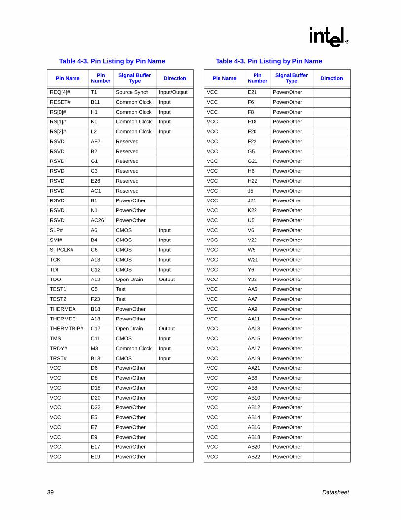
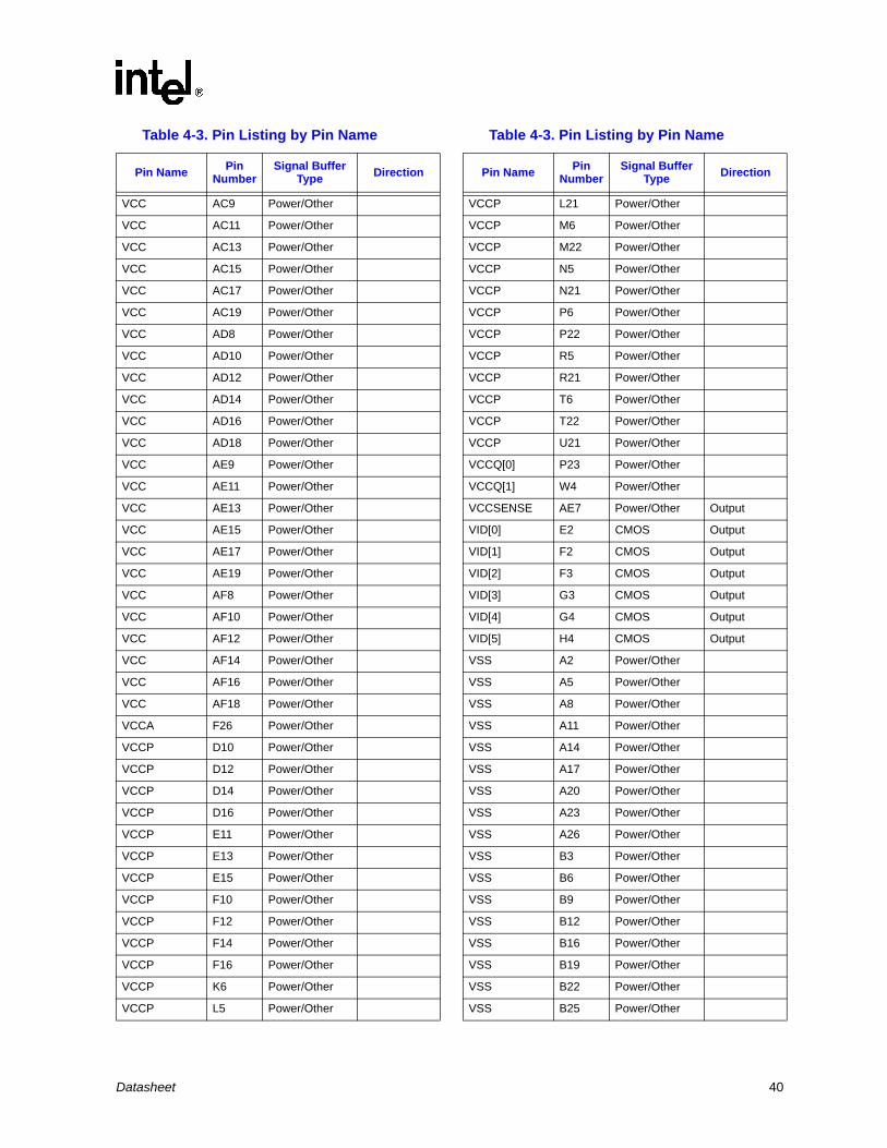
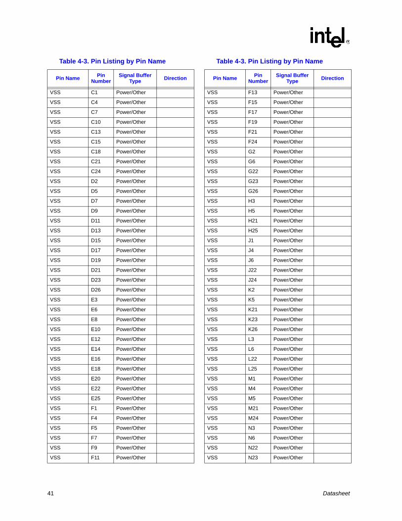
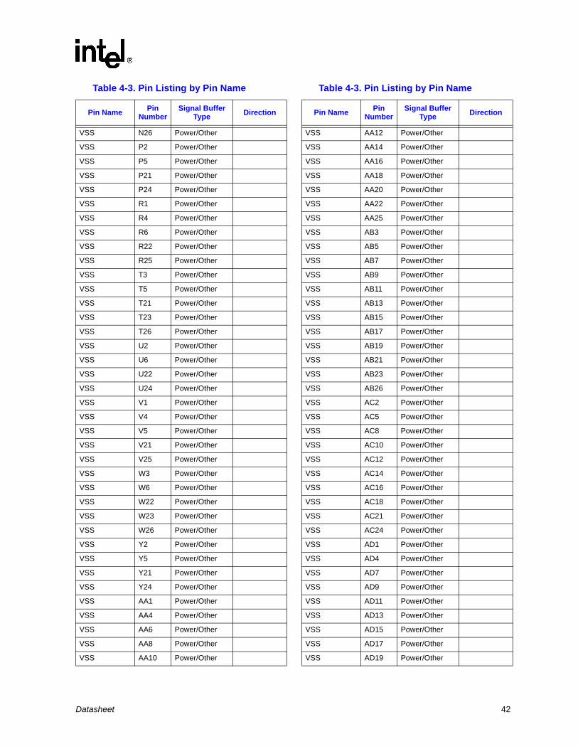
Table 4-3. Pin Listing by Pin Name
Pin Name Pin Number
Signal Buffer Type Direction
A[3]# P4 Source Synch Input/Output
A[4]# U4 Source Synch Input/Output
A[5]# V3 Source Synch Input/Output
A[6]# R3 Source Synch Input/Output
A[7]# V2 Source Synch Input/Output
A[8]# W1 Source Synch Input/Output
A[9]# T4 Source Synch Input/Output
A[10]# W2 Source Synch Input/Output
A[11]# Y4 Source Synch Input/Output
A[12]# Y1 Source Synch Input/Output
A[13]# U1 Source Synch Input/Output
A[14]# AA3 Source Synch Input/Output
A[15]# Y3 Source Synch Input/Output
A[16]# AA2 Source Synch Input/Output
A[17]# AF4 Source Synch Input/Output
A[18]# AC4 Source Synch Input/Output
A[19]# AC7 Source Synch Input/Output
A[20]# AC3 Source Synch Input/Output
A[21]# AD3 Source Synch Input/Output
A[22]# AE4 Source Synch Input/Output
A[23]# AD2 Source Synch Input/Output
A[24]# AB4 Source Synch Input/Output
A[25]# AC6 Source Synch Input/Output
A[26]# AD5 Source Synch Input/Output
A[27]# AE2 Source Synch Input/Output
A[28]# AD6 Source Synch Input/Output
A[29]# AF3 Source Synch Input/Output
A[30]# AE1 Source Synch Input/Output
A[31]# AF1 Source Synch Input/Output
A20M# C2 CMOS Input
ADS# N2 Common Clock Input/Output
ADSTB[0]# U3 Source Synch Input/Output
ADSTB[1]# AE5 Source Synch Input/Output
BCLK[0] B15 Bus Clock Input
BCLK[1] B14 Bus Clock Input
BNR# L1 Common Clock Input/Output
BPM[0]# C8 Common Clock Output
BPM[1]# B8 Common Clock Output
BPM[2]# A9 Common Clock Output
BPM[3]# C9 Common Clock Input/Output
BPRI# J3 Common Clock Input
BR0# N4 Common Clock Input/Output
BSEL[1] C14 CMOS Output
BSEL[0] C16 CMOS Output
COMP[0] P25 Power/Other Input/Output
COMP[1] P26 Power/Other Input/Output
COMP[2] AB2 Power/Other Input/Output
COMP[3] AB1 Power/Other Input/Output
D[0]# A19 Source Synch Input/Output
D[1]# A25 Source Synch Input/Output
D[2]# A22 Source Synch Input/Output
D[3]# B21 Source Synch Input/Output
D[4]# A24 Source Synch Input/Output
D[5]# B26 Source Synch Input/Output
D[6]# A21 Source Synch Input/Output
D[7]# B20 Source Synch Input/Output
D[8]# C20 Source Synch Input/Output
D[9]# B24 Source Synch Input/Output
D[10]# D24 Source Synch Input/Output
D[11]# E24 Source Synch Input/Output
D[12]# C26 Source Synch Input/Output
D[13]# B23 Source Synch Input/Output
D[14]# E23 Source Synch Input/Output
D[15]# C25 Source Synch Input/Output
D[16]# H23 Source Synch Input/Output
D[17]# G25 Source Synch Input/Output
D[18]# L23 Source Synch Input/Output
D[19]# M26 Source Synch Input/Output
D[20]# H24 Source Synch Input/Output
D[21]# F25 Source Synch Input/Output
D[22]# G24 Source Synch Input/Output
D[23]# J23 Source Synch Input/Output
D[24]# M23 Source Synch Input/Output
D[25]# J25 Source Synch Input/Output
D[26]# L26 Source Synch Input/Output
Table 4-3. Pin Listing by Pin Name
Pin Name Pin Number
Signal Buffer Type Direction

Datasheet 38
D[27]# N24 Source Synch Input/Output
D[28]# M25 Source Synch Input/Output
D[29]# H26 Source Synch Input/Output
D[30]# N25 Source Synch Input/Output
D[31]# K25 Source Synch Input/Output
D[32]# Y26 Source Synch Input/Output
D[33]# AA24 Source Synch Input/Output
D[34]# T25 Source Synch Input/Output
D[35]# U23 Source Synch Input/Output
D[36]# V23 Source Synch Input/Output
D[37]# R24 Source Synch Input/Output
D[38]# R26 Source Synch Input/Output
D[39]# R23 Source Synch Input/Output
D[40]# AA23 Source Synch Input/Output
D[41]# U26 Source Synch Input/Output
D[42]# V24 Source Synch Input/Output
D[43]# U25 Source Synch Input/Output
D[44]# V26 Source Synch Input/Output
D[45]# Y23 Source Synch Input/Output
D[46]# AA26 Source Synch Input/Output
D[47]# Y25 Source Synch Input/Output
D[48]# AB25 Source Synch Input/Output
D[49]# AC23 Source Synch Input/Output
D[50]# AB24 Source Synch Input/Output
D[51]# AC20 Source Synch Input/Output
D[52]# AC22 Source Synch Input/Output
D[53]# AC25 Source Synch Input/Output
D[54]# AD23 Source Synch Input/Output
D[55]# AE22 Source Synch Input/Output
D[56]# AF23 Source Synch Input/Output
D[57]# AD24 Source Synch Input/Output
D[58]# AF20 Source Synch Input/Output
D[59]# AE21 Source Synch Input/Output
D[60]# AD21 Source Synch Input/Output
D[61]# AF25 Source Synch Input/Output
D[62]# AF22 Source Synch Input/Output
D[63]# AF26 Source Synch Input/Output
DBR# A7 CMOS Output
Table 4-3. Pin Listing by Pin Name
Pin Name Pin Number
Signal Buffer Type Direction
DBSY# M2 Common Clock Input/Output
DEFER# L4 Common Clock Input
DINV[0]# D25 Source Synch Input/Output
DINV[1]# J26 Source Synch Input/Output
DINV[2]# T24 Source Synch Input/Output
DINV[3]# AD20 Source Synch Input/Output
DPSLP# B7 CMOS Input
DPWR# C19 Common Clock Input
DRDY# H2 Common Clock Input/Output
DSTBN[0]# C23 Source Synch Input/Output
DSTBN[1]# K24 Source Synch Input/Output
DSTBN[2]# W25 Source Synch Input/Output
DSTBN[3]# AE24 Source Synch Input/Output
DSTBP[0]# C22 Source Synch Input/Output
DSTBP[1]# L24 Source Synch Input/Output
DSTBP[2]# W24 Source Synch Input/Output
DSTBP[3]# AE25 Source Synch Input/Output
FERR# D3 Open Drain Output
GTLREF AD26 Power/Other Input
HIT# K3 Common Clock Input/Output
HITM# K4 Common Clock Input/Output
IERR# A4 Open Drain Output
IGNNE# A3 CMOS Input
INIT# B5 CMOS Input
ITP_CLK[0] A16 CMOS input
ITP_CLK[1] A15 CMOS input
LINT0 D1 CMOS Input
LINT1 D4 CMOS Input
LOCK# J2 Common Clock Input/Output
PRDY# A10 Common Clock Output
PREQ# B10 Common Clock Input
PROCHOT# B17 Open Drain Output
PSI# E1 CMOS Output
PWRGOOD E4 CMOS Input
REQ[0]# R2 Source Synch Input/Output
REQ[1]# P3 Source Synch Input/Output
REQ[2]# T2 Source Synch Input/Output
REQ[3]# P1 Source Synch Input/Output
Table 4-3. Pin Listing by Pin Name
Pin Name Pin Number
Signal Buffer Type Direction
39 Datasheet
REQ[4]# T1 Source Synch Input/Output
RESET# B11 Common Clock Input
RS[0]# H1 Common Clock Input
RS[1]# K1 Common Clock Input
RS[2]# L2 Common Clock Input
RSVD AF7 Reserved
RSVD B2 Reserved
RSVD G1 Reserved
RSVD C3 Reserved
RSVD E26 Reserved
RSVD AC1 Reserved
RSVD B1 Power/Other
RSVD N1 Power/Other
RSVD AC26 Power/Other
SLP# A6 CMOS Input
SMI# B4 CMOS Input
STPCLK# C6 CMOS Input
TCK A13 CMOS Input
TDI C12 CMOS Input
TDO A12 Open Drain Output
TEST1 C5 Test
TEST2 F23 Test
THERMDA B18 Power/Other
THERMDC A18 Power/Other
THERMTRIP# C17 Open Drain Output
TMS C11 CMOS Input
TRDY# M3 Common Clock Input
TRST# B13 CMOS Input
VCC D6 Power/Other
VCC D8 Power/Other
VCC D18 Power/Other
VCC D20 Power/Other
VCC D22 Power/Other
VCC E5 Power/Other
VCC E7 Power/Other
VCC E9 Power/Other
VCC E17 Power/Other
VCC E19 Power/Other
Table 4-3. Pin Listing by Pin Name
Pin Name Pin Number
Signal Buffer Type Direction
VCC E21 Power/Other
VCC F6 Power/Other
VCC F8 Power/Other
VCC F18 Power/Other
VCC F20 Power/Other
VCC F22 Power/Other
VCC G5 Power/Other
VCC G21 Power/Other
VCC H6 Power/Other
VCC H22 Power/Other
VCC J5 Power/Other
VCC J21 Power/Other
VCC K22 Power/Other
VCC U5 Power/Other
VCC V6 Power/Other
VCC V22 Power/Other
VCC W5 Power/Other
VCC W21 Power/Other
VCC Y6 Power/Other
VCC Y22 Power/Other
VCC AA5 Power/Other
VCC AA7 Power/Other
VCC AA9 Power/Other
VCC AA11 Power/Other
VCC AA13 Power/Other
VCC AA15 Power/Other
VCC AA17 Power/Other
VCC AA19 Power/Other
VCC AA21 Power/Other
VCC AB6 Power/Other
VCC AB8 Power/Other
VCC AB10 Power/Other
VCC AB12 Power/Other
VCC AB14 Power/Other
VCC AB16 Power/Other
VCC AB18 Power/Other
VCC AB20 Power/Other
VCC AB22 Power/Other
Table 4-3. Pin Listing by Pin Name
Pin Name Pin Number
Signal Buffer Type Direction
Datasheet 40
VCC AC9 Power/Other
VCC AC11 Power/Other
VCC AC13 Power/Other
VCC AC15 Power/Other
VCC AC17 Power/Other
VCC AC19 Power/Other
VCC AD8 Power/Other
VCC AD10 Power/Other
VCC AD12 Power/Other
VCC AD14 Power/Other
VCC AD16 Power/Other
VCC AD18 Power/Other
VCC AE9 Power/Other
VCC AE11 Power/Other
VCC AE13 Power/Other
VCC AE15 Power/Other
VCC AE17 Power/Other
VCC AE19 Power/Other
VCC AF8 Power/Other
VCC AF10 Power/Other
VCC AF12 Power/Other
VCC AF14 Power/Other
VCC AF16 Power/Other
VCC AF18 Power/Other
VCCA F26 Power/Other
VCCP D10 Power/Other
VCCP D12 Power/Other
VCCP D14 Power/Other
VCCP D16 Power/Other
VCCP E11 Power/Other
VCCP E13 Power/Other
VCCP E15 Power/Other
VCCP F10 Power/Other
VCCP F12 Power/Other
VCCP F14 Power/Other
VCCP F16 Power/Other
VCCP K6 Power/Other
VCCP L5 Power/Other
Table 4-3. Pin Listing by Pin Name
Pin Name Pin Number
Signal Buffer Type Direction
VCCP L21 Power/Other
VCCP M6 Power/Other
VCCP M22 Power/Other
VCCP N5 Power/Other
VCCP N21 Power/Other
VCCP P6 Power/Other
VCCP P22 Power/Other
VCCP R5 Power/Other
VCCP R21 Power/Other
VCCP T6 Power/Other
VCCP T22 Power/Other
VCCP U21 Power/Other
VCCQ[0] P23 Power/Other
VCCQ[1] W4 Power/Other
VCCSENSE AE7 Power/Other Output
VID[0] E2 CMOS Output
VID[1] F2 CMOS Output
VID[2] F3 CMOS Output
VID[3] G3 CMOS Output
VID[4] G4 CMOS Output
VID[5] H4 CMOS Output
VSS A2 Power/Other
VSS A5 Power/Other
VSS A8 Power/Other
VSS A11 Power/Other
VSS A14 Power/Other
VSS A17 Power/Other
VSS A20 Power/Other
VSS A23 Power/Other
VSS A26 Power/Other
VSS B3 Power/Other
VSS B6 Power/Other
VSS B9 Power/Other
VSS B12 Power/Other
VSS B16 Power/Other
VSS B19 Power/Other
VSS B22 Power/Other
VSS B25 Power/Other
Table 4-3. Pin Listing by Pin Name
Pin Name Pin Number
Signal Buffer Type Direction
41 Datasheet
VSS C1 Power/Other
VSS C4 Power/Other
VSS C7 Power/Other
VSS C10 Power/Other
VSS C13 Power/Other
VSS C15 Power/Other
VSS C18 Power/Other
VSS C21 Power/Other
VSS C24 Power/Other
VSS D2 Power/Other
VSS D5 Power/Other
VSS D7 Power/Other
VSS D9 Power/Other
VSS D11 Power/Other
VSS D13 Power/Other
VSS D15 Power/Other
VSS D17 Power/Other
VSS D19 Power/Other
VSS D21 Power/Other
VSS D23 Power/Other
VSS D26 Power/Other
VSS E3 Power/Other
VSS E6 Power/Other
VSS E8 Power/Other
VSS E10 Power/Other
VSS E12 Power/Other
VSS E14 Power/Other
VSS E16 Power/Other
VSS E18 Power/Other
VSS E20 Power/Other
VSS E22 Power/Other
VSS E25 Power/Other
VSS F1 Power/Other
VSS F4 Power/Other
VSS F5 Power/Other
VSS F7 Power/Other
VSS F9 Power/Other
VSS F11 Power/Other
Table 4-3. Pin Listing by Pin Name
Pin Name Pin Number
Signal Buffer Type Direction
VSS F13 Power/Other
VSS F15 Power/Other
VSS F17 Power/Other
VSS F19 Power/Other
VSS F21 Power/Other
VSS F24 Power/Other
VSS G2 Power/Other
VSS G6 Power/Other
VSS G22 Power/Other
VSS G23 Power/Other
VSS G26 Power/Other
VSS H3 Power/Other
VSS H5 Power/Other
VSS H21 Power/Other
VSS H25 Power/Other
VSS J1 Power/Other
VSS J4 Power/Other
VSS J6 Power/Other
VSS J22 Power/Other
VSS J24 Power/Other
VSS K2 Power/Other
VSS K5 Power/Other
VSS K21 Power/Other
VSS K23 Power/Other
VSS K26 Power/Other
VSS L3 Power/Other
VSS L6 Power/Other
VSS L22 Power/Other
VSS L25 Power/Other
VSS M1 Power/Other
VSS M4 Power/Other
VSS M5 Power/Other
VSS M21 Power/Other
VSS M24 Power/Other
VSS N3 Power/Other
VSS N6 Power/Other
VSS N22 Power/Other
VSS N23 Power/Other
Table 4-3. Pin Listing by Pin Name
Pin Name Pin Number
Signal Buffer Type Direction
Datasheet 42
VSS N26 Power/Other
VSS P2 Power/Other
VSS P5 Power/Other
VSS P21 Power/Other
VSS P24 Power/Other
VSS R1 Power/Other
VSS R4 Power/Other
VSS R6 Power/Other
VSS R22 Power/Other
VSS R25 Power/Other
VSS T3 Power/Other
VSS T5 Power/Other
VSS T21 Power/Other
VSS T23 Power/Other
VSS T26 Power/Other
VSS U2 Power/Other
VSS U6 Power/Other
VSS U22 Power/Other
VSS U24 Power/Other
VSS V1 Power/Other
VSS V4 Power/Other
VSS V5 Power/Other
VSS V21 Power/Other
VSS V25 Power/Other
VSS W3 Power/Other
VSS W6 Power/Other
VSS W22 Power/Other
VSS W23 Power/Other
VSS W26 Power/Other
VSS Y2 Power/Other
VSS Y5 Power/Other
VSS Y21 Power/Other
VSS Y24 Power/Other
VSS AA1 Power/Other
VSS AA4 Power/Other
VSS AA6 Power/Other
VSS AA8 Power/Other
VSS AA10 Power/Other
Table 4-3. Pin Listing by Pin Name
Pin Name Pin Number
Signal Buffer Type Direction
VSS AA12 Power/Other
VSS AA14 Power/Other
VSS AA16 Power/Other
VSS AA18 Power/Other
VSS AA20 Power/Other
VSS AA22 Power/Other
VSS AA25 Power/Other
VSS AB3 Power/Other
VSS AB5 Power/Other
VSS AB7 Power/Other
VSS AB9 Power/Other
VSS AB11 Power/Other
VSS AB13 Power/Other
VSS AB15 Power/Other
VSS AB17 Power/Other
VSS AB19 Power/Other
VSS AB21 Power/Other
VSS AB23 Power/Other
VSS AB26 Power/Other
VSS AC2 Power/Other
VSS AC5 Power/Other
VSS AC8 Power/Other
VSS AC10 Power/Other
VSS AC12 Power/Other
VSS AC14 Power/Other
VSS AC16 Power/Other
VSS AC18 Power/Other
VSS AC21 Power/Other
VSS AC24 Power/Other
VSS AD1 Power/Other
VSS AD4 Power/Other
VSS AD7 Power/Other
VSS AD9 Power/Other
VSS AD11 Power/Other
VSS AD13 Power/Other
VSS AD15 Power/Other
VSS AD17 Power/Other
VSS AD19 Power/Other
Table 4-3. Pin Listing by Pin Name
Pin Name Pin Number
Signal Buffer Type Direction
43 Datasheet
VSS AD22 Power/Other
VSS AD25 Power/Other
VSS AE3 Power/Other
VSS AE6 Power/Other
VSS AE8 Power/Other
VSS AE10 Power/Other
VSS AE12 Power/Other
VSS AE14 Power/Other
VSS AE16 Power/Other
VSS AE18 Power/Other
VSS AE20 Power/Other
VSS AE23 Power/Other
VSS AE26 Power/Other
VSS AF2 Power/Other
VSS AF5 Power/Other
VSS AF9 Power/Other
VSS AF11 Power/Other
VSS AF13 Power/Other
VSS AF15 Power/Other
VSS AF17 Power/Other
VSS AF19 Power/Other
VSS AF21 Power/Other
VSS AF24 Power/Other
VSSSENSE AF6 Power/Other Output
Table 4-4. Pin Listing by Pin Number
Pin Number Pin Name Signal Buffer
Type Direction
A2 VSS Power/Other
A3 IGNNE# CMOS Input
A4 IERR# Open Drain Output
A5 VSS Power/Other
A6 SLP# CMOS Input
A7 DBR# CMOS Output
A8 VSS Power/Other
A9 BPM[2]# Common Clock Output
A10 PRDY# Common Clock Output
A11 VSS Power/Other
A12 TDO Open Drain Output
Table 4-3. Pin Listing by Pin Name
Pin Name Pin Number
Signal Buffer Type Direction
A13 TCK CMOS Input
A14 VSS Power/Other
A15 ITP_CLK[1] CMOS input
A16 ITP_CLK[0] CMOS input
A17 VSS Power/Other
A18 THERMDC Power/Other
A19 D[0]# Source Synch Input/Output
A20 VSS Power/Other
A21 D[6]# Source Synch Input/Output
A22 D[2]# Source Synch Input/Output
A23 VSS Power/Other
A24 D[4]# Source Synch Input/Output
A25 D[1]# Source Synch Input/Output
A26 VSS Power/Other
AA1 VSS Power/Other
AA2 A[16]# Source Synch Input/Output
AA3 A[14]# Source Synch Input/Output
AA4 VSS Power/Other
AA5 VCC Power/Other
AA6 VSS Power/Other
AA7 VCC Power/Other
AA8 VSS Power/Other
AA9 VCC Power/Other
AA10 VSS Power/Other
AA11 VCC Power/Other
AA12 VSS Power/Other
AA13 VCC Power/Other
AA14 VSS Power/Other
AA15 VCC Power/Other
AA16 VSS Power/Other
AA17 VCC Power/Other
AA18 VSS Power/Other
AA19 VCC Power/Other
AA20 VSS Power/Other
AA21 VCC Power/Other
AA22 VSS Power/Other
AA23 D[40]# Source Synch Input/Output
AA24 D[33]# Source Synch Input/Output
Table 4-4. Pin Listing by Pin Number
Pin Number Pin Name Signal Buffer
Type Direction
Datasheet 44
AA25 VSS Power/Other
AA26 D[46]# Source Synch Input/Output
AB1 COMP[3] Power/Other Input/Output
AB2 COMP[2] Power/Other Input/Output
AB3 VSS Power/Other
AB4 A[24]# Source Synch Input/Output
AB5 VSS Power/Other
AB6 VCC Power/Other
AB7 VSS Power/Other
AB8 VCC Power/Other
AB9 VSS Power/Other
AB10 VCC Power/Other
AB11 VSS Power/Other
AB12 VCC Power/Other
AB13 VSS Power/Other
AB14 VCC Power/Other
AB15 VSS Power/Other
AB16 VCC Power/Other
AB17 VSS Power/Other
AB18 VCC Power/Other
AB19 VSS Power/Other
AB20 VCC Power/Other
AB21 VSS Power/Other
AB22 VCC Power/Other
AB23 VSS Power/Other
AB24 D[50]# Source Synch Input/Output
AB25 D[48]# Source Synch Input/Output
AB26 VSS Power/Other
AC1 RSVD Reserved
AC2 VSS Power/Other
AC3 A[20]# Source Synch Input/Output
AC4 A[18]# Source Synch Input/Output
AC5 VSS Power/Other
AC6 A[25]# Source Synch Input/Output
AC7 A[19]# Source Synch Input/Output
AC8 VSS Power/Other
AC9 VCC Power/Other
AC10 VSS Power/Other
Table 4-4. Pin Listing by Pin Number
Pin Number Pin Name Signal Buffer
Type Direction
AC11 VCC Power/Other
AC12 VSS Power/Other
AC13 VCC Power/Other
AC14 VSS Power/Other
AC15 VCC Power/Other
AC16 VSS Power/Other
AC17 VCC Power/Other
AC18 VSS Power/Other
AC19 VCC Power/Other
AC20 D[51]# Source Synch Input/Output
AC21 VSS Power/Other
AC22 D[52]# Source Synch Input/Output
AC23 D[49]# Source Synch Input/Output
AC24 VSS Power/Other
AC25 D[53]# Source Synch Input/Output
AC26 RSVD Reserved
AD1 VSS Power/Other
AD2 A[23]# Source Synch Input/Output
AD3 A[21]# Source Synch Input/Output
AD4 VSS Power/Other
AD5 A[26]# Source Synch Input/Output
AD6 A[28]# Source Synch Input/Output
AD7 VSS Power/Other
AD8 VCC Power/Other
AD9 VSS Power/Other
AD10 VCC Power/Other
AD11 VSS Power/Other
AD12 VCC Power/Other
AD13 VSS Power/Other
AD14 VCC Power/Other
AD15 VSS Power/Other
AD16 VCC Power/Other
AD17 VSS Power/Other
AD18 VCC Power/Other
AD19 VSS Power/Other
AD20 DINV[3]# Source Synch Input/Output
AD21 D[60]# Source Synch Input/Output
AD22 VSS Power/Other
Table 4-4. Pin Listing by Pin Number
Pin Number Pin Name Signal Buffer
Type Direction
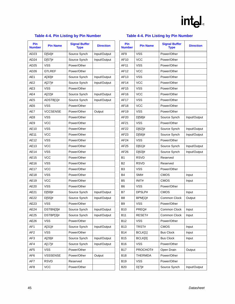
45 Datasheet
AD23 D[54]# Source Synch Input/Output
AD24 D[57]# Source Synch Input/Output
AD25 VSS Power/Other
AD26 GTLREF Power/Other
AE1 A[30]# Source Synch Input/Output
AE2 A[27]# Source Synch Input/Output
AE3 VSS Power/Other
AE4 A[22]# Source Synch Input/Output
AE5 ADSTB[1]# Source Synch Input/Output
AE6 VSS Power/Other
AE7 VCCSENSE Power/Other Output
AE8 VSS Power/Other
AE9 VCC Power/Other
AE10 VSS Power/Other
AE11 VCC Power/Other
AE12 VSS Power/Other
AE13 VCC Power/Other
AE14 VSS Power/Other
AE15 VCC Power/Other
AE16 VSS Power/Other
AE17 VCC Power/Other
AE18 VSS Power/Other
AE19 VCC Power/Other
AE20 VSS Power/Other
AE21 D[59]# Source Synch Input/Output
AE22 D[55]# Source Synch Input/Output
AE23 VSS Power/Other
AE24 DSTBN[3]# Source Synch Input/Output
AE25 DSTBP[3]# Source Synch Input/Output
AE26 VSS Power/Other
AF1 A[31]# Source Synch Input/Output
AF2 VSS Power/Other
AF3 A[29]# Source Synch Input/Output
AF4 A[17]# Source Synch Input/Output
AF5 VSS Power/Other
AF6 VSSSENSE Power/Other Output
AF7 RSVD Reserved
AF8 VCC Power/Other
Table 4-4. Pin Listing by Pin Number
Pin Number Pin Name Signal Buffer
Type Direction
AF9 VSS Power/Other
AF10 VCC Power/Other
AF11 VSS Power/Other
AF12 VCC Power/Other
AF13 VSS Power/Other
AF14 VCC Power/Other
AF15 VSS Power/Other
AF16 VCC Power/Other
AF17 VSS Power/Other
AF18 VCC Power/Other
AF19 VSS Power/Other
AF20 D[58]# Source Synch Input/Output
AF21 VSS Power/Other
AF22 D[62]# Source Synch Input/Output
AF23 D[56]# Source Synch Input/Output
AF24 VSS Power/Other
AF25 D[61]# Source Synch Input/Output
AF26 D[63]# Source Synch Input/Output
B1 RSVD Reserved
B2 RSVD Reserved
B3 VSS Power/Other
B4 SMI# CMOS Input
B5 INIT# CMOS Input
B6 VSS Power/Other
B7 DPSLP# CMOS Input
B8 BPM[1]# Common Clock Output
B9 VSS Power/Other
B10 PREQ# Common Clock Input
B11 RESET# Common Clock Input
B12 VSS Power/Other
B13 TRST# CMOS Input
B14 BCLK[1] Bus Clock Input
B15 BCLK[0] Bus Clock Input
B16 VSS Power/Other
B17 PROCHOT# Open Drain Output
B18 THERMDA Power/Other
B19 VSS Power/Other
B20 D[7]# Source Synch Input/Output
Table 4-4. Pin Listing by Pin Number
Pin Number Pin Name Signal Buffer
Type Direction
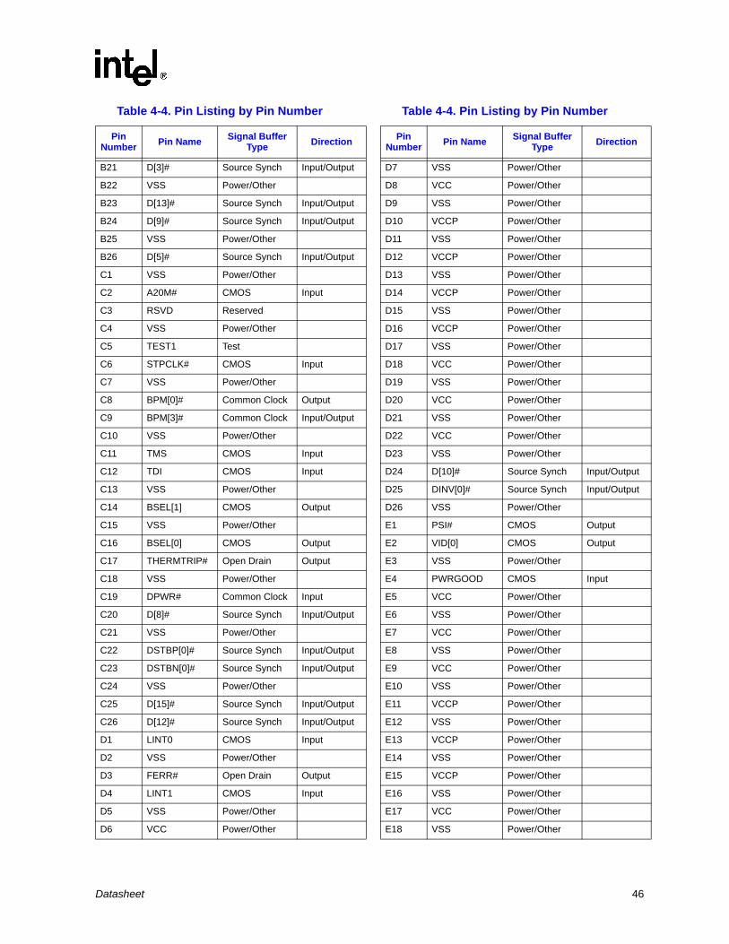
Datasheet 46
B21 D[3]# Source Synch Input/Output
B22 VSS Power/Other
B23 D[13]# Source Synch Input/Output
B24 D[9]# Source Synch Input/Output
B25 VSS Power/Other
B26 D[5]# Source Synch Input/Output
C1 VSS Power/Other
C2 A20M# CMOS Input
C3 RSVD Reserved
C4 VSS Power/Other
C5 TEST1 Test
C6 STPCLK# CMOS Input
C7 VSS Power/Other
C8 BPM[0]# Common Clock Output
C9 BPM[3]# Common Clock Input/Output
C10 VSS Power/Other
C11 TMS CMOS Input
C12 TDI CMOS Input
C13 VSS Power/Other
C14 BSEL[1] CMOS Output
C15 VSS Power/Other
C16 BSEL[0] CMOS Output
C17 THERMTRIP# Open Drain Output
C18 VSS Power/Other
C19 DPWR# Common Clock Input
C20 D[8]# Source Synch Input/Output
C21 VSS Power/Other
C22 DSTBP[0]# Source Synch Input/Output
C23 DSTBN[0]# Source Synch Input/Output
C24 VSS Power/Other
C25 D[15]# Source Synch Input/Output
C26 D[12]# Source Synch Input/Output
D1 LINT0 CMOS Input
D2 VSS Power/Other
D3 FERR# Open Drain Output
D4 LINT1 CMOS Input
D5 VSS Power/Other
D6 VCC Power/Other
Table 4-4. Pin Listing by Pin Number
Pin Number Pin Name Signal Buffer
Type Direction
D7 VSS Power/Other
D8 VCC Power/Other
D9 VSS Power/Other
D10 VCCP Power/Other
D11 VSS Power/Other
D12 VCCP Power/Other
D13 VSS Power/Other
D14 VCCP Power/Other
D15 VSS Power/Other
D16 VCCP Power/Other
D17 VSS Power/Other
D18 VCC Power/Other
D19 VSS Power/Other
D20 VCC Power/Other
D21 VSS Power/Other
D22 VCC Power/Other
D23 VSS Power/Other
D24 D[10]# Source Synch Input/Output
D25 DINV[0]# Source Synch Input/Output
D26 VSS Power/Other
E1 PSI# CMOS Output
E2 VID[0] CMOS Output
E3 VSS Power/Other
E4 PWRGOOD CMOS Input
E5 VCC Power/Other
E6 VSS Power/Other
E7 VCC Power/Other
E8 VSS Power/Other
E9 VCC Power/Other
E10 VSS Power/Other
E11 VCCP Power/Other
E12 VSS Power/Other
E13 VCCP Power/Other
E14 VSS Power/Other
E15 VCCP Power/Other
E16 VSS Power/Other
E17 VCC Power/Other
E18 VSS Power/Other
Table 4-4. Pin Listing by Pin Number
Pin Number Pin Name Signal Buffer
Type Direction
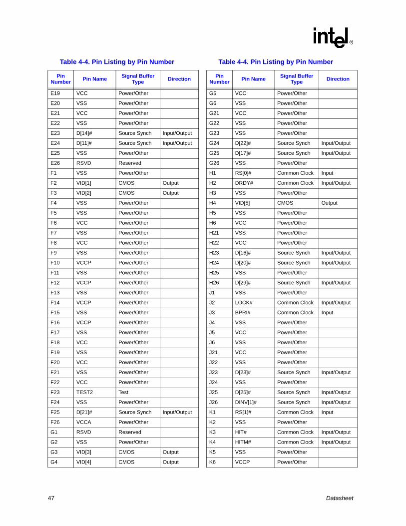
47 Datasheet
E19 VCC Power/Other
E20 VSS Power/Other
E21 VCC Power/Other
E22 VSS Power/Other
E23 D[14]# Source Synch Input/Output
E24 D[11]# Source Synch Input/Output
E25 VSS Power/Other
E26 RSVD Reserved
F1 VSS Power/Other
F2 VID[1] CMOS Output
F3 VID[2] CMOS Output
F4 VSS Power/Other
F5 VSS Power/Other
F6 VCC Power/Other
F7 VSS Power/Other
F8 VCC Power/Other
F9 VSS Power/Other
F10 VCCP Power/Other
F11 VSS Power/Other
F12 VCCP Power/Other
F13 VSS Power/Other
F14 VCCP Power/Other
F15 VSS Power/Other
F16 VCCP Power/Other
F17 VSS Power/Other
F18 VCC Power/Other
F19 VSS Power/Other
F20 VCC Power/Other
F21 VSS Power/Other
F22 VCC Power/Other
F23 TEST2 Test
F24 VSS Power/Other
F25 D[21]# Source Synch Input/Output
F26 VCCA Power/Other
G1 RSVD Reserved
G2 VSS Power/Other
G3 VID[3] CMOS Output
G4 VID[4] CMOS Output
Table 4-4. Pin Listing by Pin Number
Pin Number Pin Name Signal Buffer
Type Direction
G5 VCC Power/Other
G6 VSS Power/Other
G21 VCC Power/Other
G22 VSS Power/Other
G23 VSS Power/Other
G24 D[22]# Source Synch Input/Output
G25 D[17]# Source Synch Input/Output
G26 VSS Power/Other
H1 RS[0]# Common Clock Input
H2 DRDY# Common Clock Input/Output
H3 VSS Power/Other
H4 VID[5] CMOS Output
H5 VSS Power/Other
H6 VCC Power/Other
H21 VSS Power/Other
H22 VCC Power/Other
H23 D[16]# Source Synch Input/Output
H24 D[20]# Source Synch Input/Output
H25 VSS Power/Other
H26 D[29]# Source Synch Input/Output
J1 VSS Power/Other
J2 LOCK# Common Clock Input/Output
J3 BPRI# Common Clock Input
J4 VSS Power/Other
J5 VCC Power/Other
J6 VSS Power/Other
J21 VCC Power/Other
J22 VSS Power/Other
J23 D[23]# Source Synch Input/Output
J24 VSS Power/Other
J25 D[25]# Source Synch Input/Output
J26 DINV[1]# Source Synch Input/Output
K1 RS[1]# Common Clock Input
K2 VSS Power/Other
K3 HIT# Common Clock Input/Output
K4 HITM# Common Clock Input/Output
K5 VSS Power/Other
K6 VCCP Power/Other
Table 4-4. Pin Listing by Pin Number
Pin Number Pin Name Signal Buffer
Type Direction

Datasheet 48
K21 VSS Power/Other
K22 VCC Power/Other
K23 VSS Power/Other
K24 DSTBN[1]# Source Synch Input/Output
K25 D[31]# Source Synch Input/Output
K26 VSS Power/Other
L1 BNR# Common Clock Input/Output
L2 RS[2]# Common Clock Input
L3 VSS Power/Other
L4 DEFER# Common Clock Input
L5 VCCP Power/Other
L6 VSS Power/Other
L21 VCCP Power/Other
L22 VSS Power/Other
L23 D[18]# Source Synch Input/Output
L24 DSTBP[1]# Source Synch Input/Output
L25 VSS Power/Other
L26 D[26]# Source Synch Input/Output
M1 VSS Power/Other
M2 DBSY# Common Clock Input/Output
M3 TRDY# Common Clock Input
M4 VSS Power/Other
M5 VSS Power/Other
M6 VCCP Power/Other
M21 VSS Power/Other
M22 VCCP Power/Other
M23 D[24]# Source Synch Input/Output
M24 VSS Power/Other
M25 D[28]# Source Synch Input/Output
M26 D[19]# Source Synch Input/Output
N1 RSVD Reserved
N2 ADS# Common Clock Input/Output
N3 VSS Power/Other
N4 BR0# Common Clock Input/Output
N5 VCCP Power/Other
N6 VSS Power/Other
N21 VCCP Power/Other
N22 VSS Power/Other
Table 4-4. Pin Listing by Pin Number
Pin Number Pin Name Signal Buffer
Type Direction
N23 VSS Power/Other
N24 D[27]# Source Synch Input/Output
N25 D[30]# Source Synch Input/Output
N26 VSS Power/Other
P1 REQ[3]# Source Synch Input/Output
P2 VSS Power/Other
P3 REQ[1]# Source Synch Input/Output
P4 A[3]# Source Synch Input/Output
P5 VSS Power/Other
P6 VCCP Power/Other
P21 VSS Power/Other
P22 VCCP Power/Other
P23 VCCQ[0] Power/Other
P24 VSS Power/Other
P25 COMP[0] Power/Other Input/Output
P26 COMP[1] Power/Other Input/Output
R1 VSS Power/Other
R2 REQ[0]# Source Synch Input/Output
R3 A[6]# Source Synch Input/Output
R4 VSS Power/Other
R5 VCCP Power/Other
R6 VSS Power/Other
R21 VCCP Power/Other
R22 VSS Power/Other
R23 D[39]# Source Synch Input/Output
R24 D[37]# Source Synch Input/Output
R25 VSS Power/Other
R26 D[38]# Source Synch Input/Output
T1 REQ[4]# Source Synch Input/Output
T2 REQ[2]# Source Synch Input/Output
T3 VSS Power/Other
T4 A[9]# Source Synch Input/Output
T5 VSS Power/Other
T6 VCCP Power/Other
T21 VSS Power/Other
T22 VCCP Power/Other
T23 VSS Power/Other
T24 DINV[2]# CMOS Input/Output
Table 4-4. Pin Listing by Pin Number
Pin Number Pin Name Signal Buffer
Type Direction

49 Datasheet
T25 D[34]# Source Synch Input/Output
T26 VSS Power/Other
U1 A[13]# Source Synch Input/Output
U2 VSS Power/Other
U3 ADSTB[0]# Source Synch Input/Output
U4 A[4]# Source Synch Input/Output
U5 VCC Power/Other
U6 VSS Power/Other
U21 VCCP Power/Other
U22 VSS Power/Other
U23 D[35]# Source Synch Input/Output
U24 VSS Power/Other
U25 D[43]# Source Synch Input/Output
U26 D[41]# Source Synch Input/Output
V1 VSS Power/Other
V2 A[7]# Source Synch Input/Output
V3 A[5]# Source Synch Input/Output
V4 VSS Power/Other
V5 VSS Power/Other
V6 VCC Power/Other
V21 VSS Power/Other
V22 VCC Power/Other
V23 D[36]# Source Synch Input/Output
V24 D[42]# Source Synch Input/Output
V25 VSS Power/Other
V26 D[44]# Source Synch Input/Output
W1 A[8]# Source Synch Input/Output
W2 A[10]# Source Synch Input/Output
W3 VSS Power/Other
W4 VCCQ[1] Power/Other
W5 VCC Power/Other
W6 VSS Power/Other
W21 VCC Power/Other
W22 VSS Power/Other
W23 VSS Power/Other
W24 DSTBP[2]# Source Synch Input/Output
W25 DSTBN[2]# Source Synch Input/Output
W26 VSS Power/Other
Table 4-4. Pin Listing by Pin Number
Pin Number Pin Name Signal Buffer
Type Direction
Y1 A[12]# Source Synch Input/Output
Y2 VSS Power/Other
Y3 A[15]# Source Synch Input/Output
Y4 A[11]# Source Synch Input/Output
Y5 VSS Power/Other
Y6 VCC Power/Other
Y21 VSS Power/Other
Y22 VCC Power/Other
Y23 D[45]# Source Synch Input/Output
Y24 VSS Power/Other
Y25 D[47]# Source Synch Input/Output
Y26 D[32]# Source Synch Input/Output
Table 4-4. Pin Listing by Pin Number
Pin Number Pin Name Signal Buffer
Type Direction

50 Datasheet
Contents
This page is intentionally left blank.§
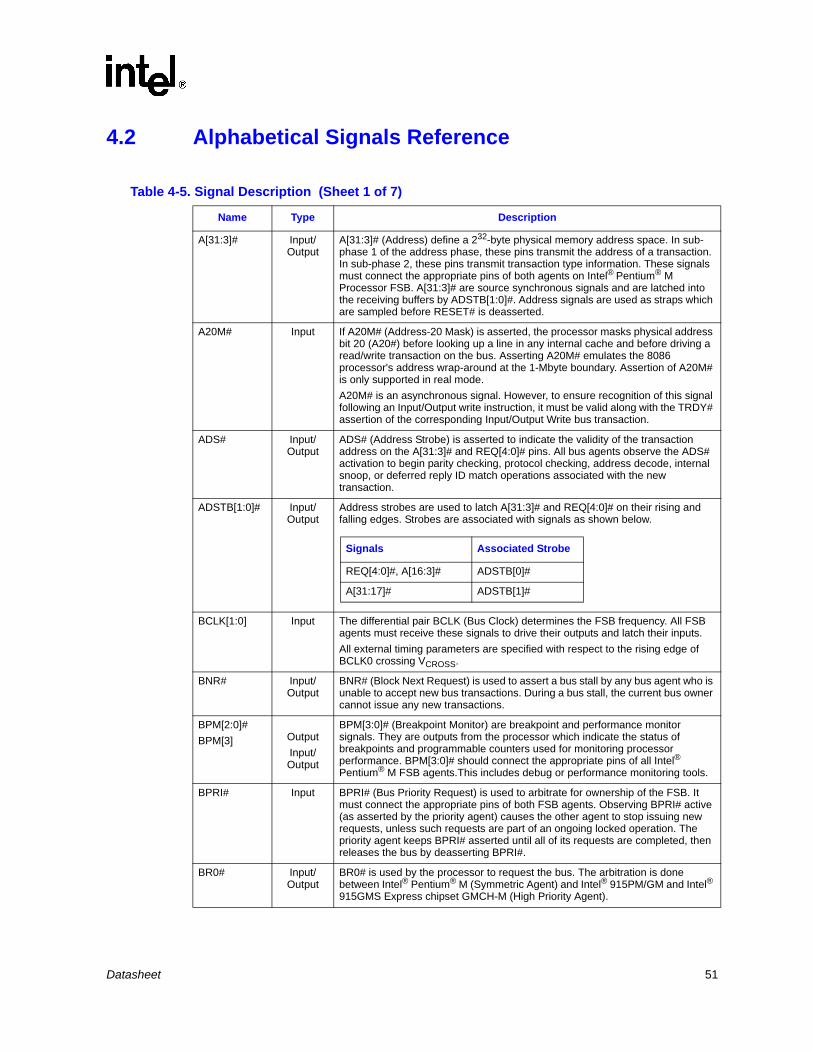
Datasheet 51
4.2 Alphabetical Signals Reference
Table 4-5. Signal Description (Sheet 1 of 7)
Name Type Description
A[31:3]# Input/Output
A[31:3]# (Address) define a 232-byte physical memory address space. In sub-phase 1 of the address phase, these pins transmit the address of a transaction. In sub-phase 2, these pins transmit transaction type information. These signals must connect the appropriate pins of both agents on Intel® Pentium® M Processor FSB. A[31:3]# are source synchronous signals and are latched into the receiving buffers by ADSTB[1:0]#. Address signals are used as straps which are sampled before RESET# is deasserted.
A20M# Input If A20M# (Address-20 Mask) is asserted, the processor masks physical address bit 20 (A20#) before looking up a line in any internal cache and before driving a read/write transaction on the bus. Asserting A20M# emulates the 8086 processor's address wrap-around at the 1-Mbyte boundary. Assertion of A20M# is only supported in real mode.A20M# is an asynchronous signal. However, to ensure recognition of this signal following an Input/Output write instruction, it must be valid along with the TRDY# assertion of the corresponding Input/Output Write bus transaction.
ADS# Input/Output
ADS# (Address Strobe) is asserted to indicate the validity of the transaction address on the A[31:3]# and REQ[4:0]# pins. All bus agents observe the ADS# activation to begin parity checking, protocol checking, address decode, internal snoop, or deferred reply ID match operations associated with the new transaction.
ADSTB[1:0]# Input/Output
Address strobes are used to latch A[31:3]# and REQ[4:0]# on their rising and falling edges. Strobes are associated with signals as shown below.
BCLK[1:0] Input The differential pair BCLK (Bus Clock) determines the FSB frequency. All FSB agents must receive these signals to drive their outputs and latch their inputs.All external timing parameters are specified with respect to the rising edge of BCLK0 crossing VCROSS.
BNR# Input/Output
BNR# (Block Next Request) is used to assert a bus stall by any bus agent who is unable to accept new bus transactions. During a bus stall, the current bus owner cannot issue any new transactions.
BPM[2:0]#BPM[3] Output
Input/Output
BPM[3:0]# (Breakpoint Monitor) are breakpoint and performance monitor signals. They are outputs from the processor which indicate the status of breakpoints and programmable counters used for monitoring processor performance. BPM[3:0]# should connect the appropriate pins of all Intel® Pentium® M FSB agents.This includes debug or performance monitoring tools.
BPRI# Input BPRI# (Bus Priority Request) is used to arbitrate for ownership of the FSB. It must connect the appropriate pins of both FSB agents. Observing BPRI# active (as asserted by the priority agent) causes the other agent to stop issuing new requests, unless such requests are part of an ongoing locked operation. The priority agent keeps BPRI# asserted until all of its requests are completed, then releases the bus by deasserting BPRI#.
BR0# Input/Output
BR0# is used by the processor to request the bus. The arbitration is done between Intel® Pentium® M (Symmetric Agent) and Intel® 915PM/GM and Intel® 915GMS Express chipset GMCH-M (High Priority Agent).
Signals Associated Strobe
REQ[4:0]#, A[16:3]# ADSTB[0]#
A[31:17]# ADSTB[1]#

52 Datasheet
BSEL[1:0] Output BSEL[1:0] (Bus Select) are used to select the processor input clock frequency. Table 3-2 defines the possible combinations of the signals and the frequency associated with each combination. The required frequency is determined by the processor, chipset and clock synthesizer. All agents must operate at the same frequency. The Pentium M Processor operates at a 533-MHz front side bus frequency (133 MHz BCLK).
COMP[3:0] Analog COMP[3:0] must be terminated on the system board using precision (1% tolerance) resistors.
D[63:0]# Input/Output
D[63:0]# (Data) are the data signals. These signals provide a 64-bit data path between the FSB agents, and must connect the appropriate pins on both agents. The data driver asserts DRDY# to indicate a valid data transfer.D[63:0]# are quad-pumped signals and will thus be driven four times in a common clock period. D[63:0]# are latched off the falling edge of both DSTBP[3:0]# and DSTBN[3:0]#. Each group of 16 data signals correspond to a pair of one DSTBP# and one DSTBN#. The following table shows the grouping of data signals to data strobes and DINV#.
Furthermore, the DINV# pins determine the polarity of the data signals. Each group of 16 data signals corresponds to one DINV# signal. When the DINV# signal is active, the corresponding data group is inverted and therefore sampled active high.
DBR# Output DBR# (Data Bus Reset) is used only in processor systems where no debug port is implemented on the system board. DBR# is used by a debug port interposer so that an in-target probe can drive system reset. If a debug port is implemented in the system, DBR# is a no connect in the system. DBR# is not a processor signal.
DBSY# Input/Output
DBSY# (Data Bus Busy) is asserted by the agent responsible for driving data on the FSB to indicate that the data bus is in use. The data bus is released after DBSY# is deasserted. This signal must connect the appropriate pins on both FSB agents.
DEFER# Input DEFER# is asserted by an agent to indicate that a transaction cannot be guaranteed in-order completion. Assertion of DEFER# is normally the responsibility of the addressed memory or Input/Output agent. This signal must connect the appropriate pins of both FSB agents.
Table 4-5. Signal Description (Sheet 2 of 7)
Name Type Description
Quad-Pumped Signal Groups
Data Group DSTBN#/DSTBP# DINV#
D[15:0]# 0 0
D[31:16]# 1 1
D[47:32]# 2 2
D[63:48]# 3 3
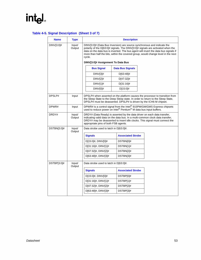
Datasheet 53
DINV[3:0]# Input/Output
DINV[3:0]# (Data Bus Inversion) are source synchronous and indicate the polarity of the D[63:0]# signals. The DINV[3:0]# signals are activated when the data on the data bus is inverted. The bus agent will invert the data bus signals if more than half the bits, within the covered group, would change level in the next cycle.
DPSLP# Input DPSLP# when asserted on the platform causes the processor to transition from the Sleep State to the Deep Sleep state. In order to return to the Sleep State, DPSLP# must be deasserted. DPSLP# is driven by the ICH6-M chipset.
DPWR# Input DPWR# is a control signal from the Intel® 915PM/GM/GMS Express chipsets used to reduce power on Intel® Pentium® M data bus input buffers.
DRDY# Input/Output
DRDY# (Data Ready) is asserted by the data driver on each data transfer, indicating valid data on the data bus. In a multi-common clock data transfer, DRDY# may be deasserted to insert idle clocks. This signal must connect the appropriate pins of both FSB agents.
DSTBN[3:0]# Input/Output
Data strobe used to latch in D[63:0]#.
DSTBP[3:0]# Input/Output
Data strobe used to latch in D[63:0]#.
Table 4-5. Signal Description (Sheet 3 of 7)
Name Type Description
DINV[3:0]# Assignment To Data Bus
Bus Signal Data Bus Signals
DINV[3]# D[63:48]#
DINV[2]# D[47:32]#
DINV[1]# D[31:16]#
DINV[0]# D[15:0]#
Signals Associated Strobe
D[15:0]#, DINV[0]# DSTBN[0]#
D[31:16]#, DINV[1]# DSTBN[1]#
D[47:32]#, DINV[2]# DSTBN[2]#
D[63:48]#, DINV[3]# DSTBN[3]#
Signals Associated Strobe
D[15:0]#, DINV[0]# DSTBP[0]#
D[31:16]#, DINV[1]# DSTBP[1]#
D[47:32]#, DINV[2]# DSTBP[2]#
D[63:48]#, DINV[3]# DSTBP[3]#
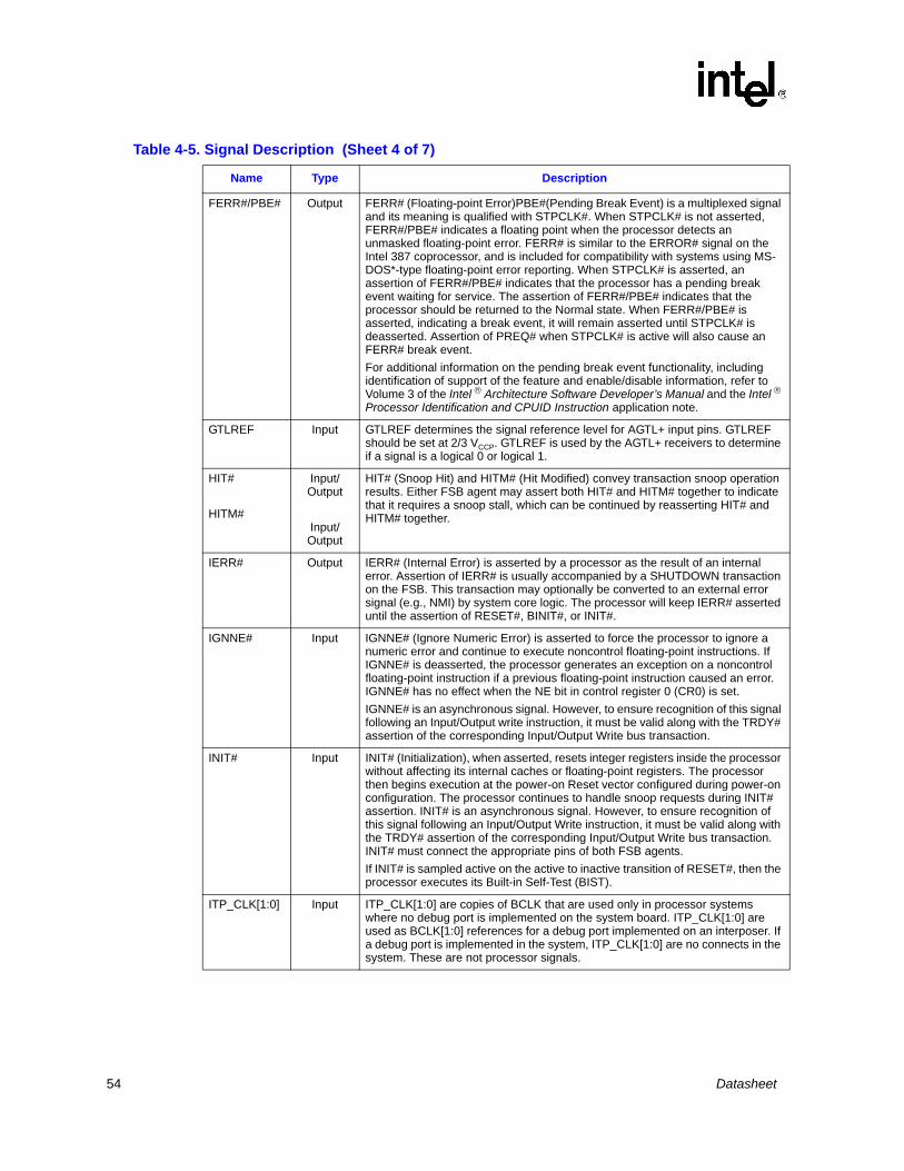
54 Datasheet
FERR#/PBE# Output FERR# (Floating-point Error)PBE#(Pending Break Event) is a multiplexed signal and its meaning is qualified with STPCLK#. When STPCLK# is not asserted, FERR#/PBE# indicates a floating point when the processor detects an unmasked floating-point error. FERR# is similar to the ERROR# signal on the Intel 387 coprocessor, and is included for compatibility with systems using MS-DOS*-type floating-point error reporting. When STPCLK# is asserted, an assertion of FERR#/PBE# indicates that the processor has a pending break event waiting for service. The assertion of FERR#/PBE# indicates that the processor should be returned to the Normal state. When FERR#/PBE# is asserted, indicating a break event, it will remain asserted until STPCLK# is deasserted. Assertion of PREQ# when STPCLK# is active will also cause an FERR# break event. For additional information on the pending break event functionality, including identification of support of the feature and enable/disable information, refer to Volume 3 of the Intel ® Architecture Software Developer’s Manual and the Intel ®
Processor Identification and CPUID Instruction application note.
GTLREF Input GTLREF determines the signal reference level for AGTL+ input pins. GTLREF should be set at 2/3 VCCP. GTLREF is used by the AGTL+ receivers to determine if a signal is a logical 0 or logical 1.
HIT#
HITM#
Input/Output
Input/Output
HIT# (Snoop Hit) and HITM# (Hit Modified) convey transaction snoop operation results. Either FSB agent may assert both HIT# and HITM# together to indicate that it requires a snoop stall, which can be continued by reasserting HIT# and HITM# together.
IERR# Output IERR# (Internal Error) is asserted by a processor as the result of an internal error. Assertion of IERR# is usually accompanied by a SHUTDOWN transaction on the FSB. This transaction may optionally be converted to an external error signal (e.g., NMI) by system core logic. The processor will keep IERR# asserted until the assertion of RESET#, BINIT#, or INIT#.
IGNNE# Input IGNNE# (Ignore Numeric Error) is asserted to force the processor to ignore a numeric error and continue to execute noncontrol floating-point instructions. If IGNNE# is deasserted, the processor generates an exception on a noncontrol floating-point instruction if a previous floating-point instruction caused an error. IGNNE# has no effect when the NE bit in control register 0 (CR0) is set.IGNNE# is an asynchronous signal. However, to ensure recognition of this signal following an Input/Output write instruction, it must be valid along with the TRDY# assertion of the corresponding Input/Output Write bus transaction.
INIT# Input INIT# (Initialization), when asserted, resets integer registers inside the processor without affecting its internal caches or floating-point registers. The processor then begins execution at the power-on Reset vector configured during power-on configuration. The processor continues to handle snoop requests during INIT# assertion. INIT# is an asynchronous signal. However, to ensure recognition of this signal following an Input/Output Write instruction, it must be valid along with the TRDY# assertion of the corresponding Input/Output Write bus transaction. INIT# must connect the appropriate pins of both FSB agents.If INIT# is sampled active on the active to inactive transition of RESET#, then the processor executes its Built-in Self-Test (BIST).
ITP_CLK[1:0] Input ITP_CLK[1:0] are copies of BCLK that are used only in processor systems where no debug port is implemented on the system board. ITP_CLK[1:0] are used as BCLK[1:0] references for a debug port implemented on an interposer. If a debug port is implemented in the system, ITP_CLK[1:0] are no connects in the system. These are not processor signals.
Table 4-5. Signal Description (Sheet 4 of 7)
Name Type Description
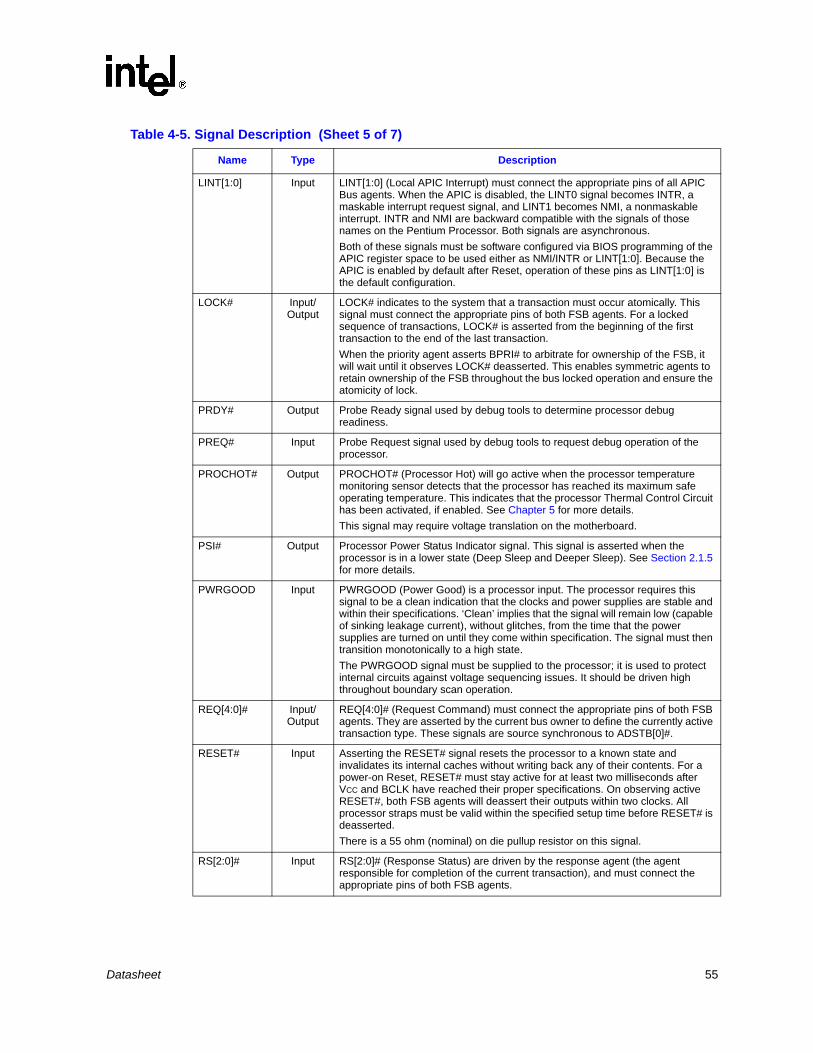
Datasheet 55
LINT[1:0] Input LINT[1:0] (Local APIC Interrupt) must connect the appropriate pins of all APIC Bus agents. When the APIC is disabled, the LINT0 signal becomes INTR, a maskable interrupt request signal, and LINT1 becomes NMI, a nonmaskable interrupt. INTR and NMI are backward compatible with the signals of those names on the Pentium Processor. Both signals are asynchronous.Both of these signals must be software configured via BIOS programming of the APIC register space to be used either as NMI/INTR or LINT[1:0]. Because the APIC is enabled by default after Reset, operation of these pins as LINT[1:0] is the default configuration.
LOCK# Input/Output
LOCK# indicates to the system that a transaction must occur atomically. This signal must connect the appropriate pins of both FSB agents. For a locked sequence of transactions, LOCK# is asserted from the beginning of the first transaction to the end of the last transaction.When the priority agent asserts BPRI# to arbitrate for ownership of the FSB, it will wait until it observes LOCK# deasserted. This enables symmetric agents to retain ownership of the FSB throughout the bus locked operation and ensure the atomicity of lock.
PRDY# Output Probe Ready signal used by debug tools to determine processor debug readiness.
PREQ# Input Probe Request signal used by debug tools to request debug operation of the processor.
PROCHOT# Output PROCHOT# (Processor Hot) will go active when the processor temperature monitoring sensor detects that the processor has reached its maximum safe operating temperature. This indicates that the processor Thermal Control Circuit has been activated, if enabled. See Chapter 5 for more details.This signal may require voltage translation on the motherboard.
PSI# Output Processor Power Status Indicator signal. This signal is asserted when the processor is in a lower state (Deep Sleep and Deeper Sleep). See Section 2.1.5 for more details.
PWRGOOD Input PWRGOOD (Power Good) is a processor input. The processor requires this signal to be a clean indication that the clocks and power supplies are stable and within their specifications. ‘Clean’ implies that the signal will remain low (capable of sinking leakage current), without glitches, from the time that the power supplies are turned on until they come within specification. The signal must then transition monotonically to a high state. The PWRGOOD signal must be supplied to the processor; it is used to protect internal circuits against voltage sequencing issues. It should be driven high throughout boundary scan operation.
REQ[4:0]# Input/Output
REQ[4:0]# (Request Command) must connect the appropriate pins of both FSB agents. They are asserted by the current bus owner to define the currently active transaction type. These signals are source synchronous to ADSTB[0]#.
RESET# Input Asserting the RESET# signal resets the processor to a known state and invalidates its internal caches without writing back any of their contents. For a power-on Reset, RESET# must stay active for at least two milliseconds after VCC and BCLK have reached their proper specifications. On observing active RESET#, both FSB agents will deassert their outputs within two clocks. All processor straps must be valid within the specified setup time before RESET# is deasserted.There is a 55 ohm (nominal) on die pullup resistor on this signal.
RS[2:0]# Input RS[2:0]# (Response Status) are driven by the response agent (the agent responsible for completion of the current transaction), and must connect the appropriate pins of both FSB agents.
Table 4-5. Signal Description (Sheet 5 of 7)
Name Type Description
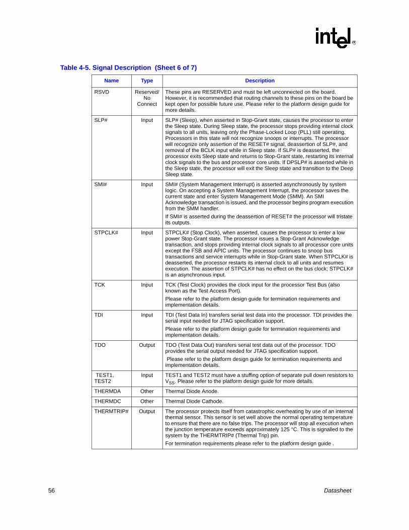
56 Datasheet
RSVD Reserved/No
Connect
These pins are RESERVED and must be left unconnected on the board. However, it is recommended that routing channels to these pins on the board be kept open for possible future use. Please refer to the platform design guide for more details.
SLP# Input SLP# (Sleep), when asserted in Stop-Grant state, causes the processor to enter the Sleep state. During Sleep state, the processor stops providing internal clock signals to all units, leaving only the Phase-Locked Loop (PLL) still operating. Processors in this state will not recognize snoops or interrupts. The processor will recognize only assertion of the RESET# signal, deassertion of SLP#, and removal of the BCLK input while in Sleep state. If SLP# is deasserted, the processor exits Sleep state and returns to Stop-Grant state, restarting its internal clock signals to the bus and processor core units. If DPSLP# is asserted while in the Sleep state, the processor will exit the Sleep state and transition to the Deep Sleep state.
SMI# Input SMI# (System Management Interrupt) is asserted asynchronously by system logic. On accepting a System Management Interrupt, the processor saves the current state and enter System Management Mode (SMM). An SMI Acknowledge transaction is issued, and the processor begins program execution from the SMM handler.If SMI# is asserted during the deassertion of RESET# the processor will tristate its outputs.
STPCLK# Input STPCLK# (Stop Clock), when asserted, causes the processor to enter a low power Stop-Grant state. The processor issues a Stop-Grant Acknowledge transaction, and stops providing internal clock signals to all processor core units except the FSB and APIC units. The processor continues to snoop bus transactions and service interrupts while in Stop-Grant state. When STPCLK# is deasserted, the processor restarts its internal clock to all units and resumes execution. The assertion of STPCLK# has no effect on the bus clock; STPCLK# is an asynchronous input.
TCK Input TCK (Test Clock) provides the clock input for the processor Test Bus (also known as the Test Access Port). Please refer to the platform design guide for termination requirements and implementation details.
TDI Input TDI (Test Data In) transfers serial test data into the processor. TDI provides the serial input needed for JTAG specification support.Please refer to the platform design guide for termination requirements and implementation details.
TDO Output TDO (Test Data Out) transfers serial test data out of the processor. TDO provides the serial output needed for JTAG specification support. Please refer to the platform design guide for termination requirements and implementation details.
TEST1, TEST2
Input TEST1 and TEST2 must have a stuffing option of separate pull down resistors to VSS. Please refer to the platform design guide for more details.
THERMDA Other Thermal Diode Anode.
THERMDC Other Thermal Diode Cathode.
THERMTRIP# Output The processor protects itself from catastrophic overheating by use of an internal thermal sensor. This sensor is set well above the normal operating temperature to ensure that there are no false trips. The processor will stop all execution when the junction temperature exceeds approximately 125 °C. This is signalled to the system by the THERMTRIP# (Thermal Trip) pin.For termination requirements please refer to the platform design guide .
Table 4-5. Signal Description (Sheet 6 of 7)
Name Type Description
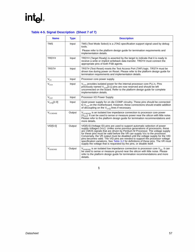
Datasheet 57
§
TMS Input TMS (Test Mode Select) is a JTAG specification support signal used by debug tools. Please refer to the platform design guide for termination requirements and implementation details.
TRDY# Input TRDY# (Target Ready) is asserted by the target to indicate that it is ready to receive a write or implicit writeback data transfer. TRDY# must connect the appropriate pins of both FSB agents.
TRST# Input TRST# (Test Reset) resets the Test Access Port (TAP) logic. TRST# must be driven low during power on Reset. Please refer to the platform design guide for termination requirements and implementation details.
VCC Input Processor core power supply.
VCCA Input VCCA provides isolated power for the internal processor core PLL’s. Pins previously named VCCA[3:1] pins are now reserved and should be left unconnected on the board. Refer to the platform design guide for complete implementation details.
VCCP Input Processor I/O Power Supply.
VCCQ[1:0] Input Quiet power supply for on die COMP circuitry. These pins should be connected to VCCP on the motherboard. However, these connections should enable addition of decoupling on the VCCQ lines if necessary.
VCCSENSE Output VCCSENSE is an isolated low impedance connection to processor core power (VCC). It can be used to sense or measure power near the silicon with little noise. Please refer to the platform design guide for termination recommendations and more details.
VID[5:0] Output VID[5:0] (Voltage ID) pins are used to support automatic selection of power supply voltages (Vcc). Unlike some previous generations of processors, these are CMOS signals that are driven by Pentium M Processor. The voltage supply for these pins must be valid before the VR can supply Vcc to the processor. Conversely, the VR output must be disabled until the voltage supply for the VID pins becomes valid. The VID pins are needed to support the processor voltage specification variations. See Table 3-2 for definitions of these pins. The VR must supply the voltage that is requested by the pins, or disable itself.
VSSSENSE Output VSSSENSE is an isolated low impedance connection to processor core VSS. It can be used to sense or measure ground near the silicon with little noise. Please refer to the platform design guide for termination recommendations and more details.
Table 4-5. Signal Description (Sheet 7 of 7)
Name Type Description

58 Datasheet
Datasheet 59
Thermal Specifications and Design Considerations
5 Thermal Specifications and Design Considerations
The Pentium M Processor requires a thermal solution to maintain temperatures within operating limits as set forth in Section 5.1. Any attempt to operate that processor outside these operating limits may result in permanent damage to the processor and potentially other components in the system. As processor technology changes, thermal management becomes increasingly crucial when building computer systems. Maintaining the proper thermal environment is key to reliable, long-term system operation. A complete thermal solution includes both component and system level thermal management features. Component level thermal solutions include active or passive heatsinks or heat exchangers attached to the processor exposed die. The solution should make firm contact to the die while maintaining processor mechanical specifications such as pressure. A typical system level thermal solution may consist of a processor fan ducted to a heat exchanger that is thermally coupled to the processor via a heat pipe or direct die attachment. A secondary fan or air from the processor fan may also be used to cool other platform components or lower the internal ambient temperature within the system.
To allow for the optimal operation and long-term reliability of Intel processor-based systems, the system/processor thermal solution should be designed such that the processor must remain within the minimum and maximum junction temperature (Tj) specifications at the corresponding thermal design power (TDP) value listed in Table 5-1. Thermal solutions not design to provide this level of thermal capability may affect the long-term reliability of the processor and system.
The maximum junction temperature is defined by an activation of the processor Intel® Thermal Monitor. Refer to Section 5.1.3 for more details. Analysis indicates that real applications are unlikely to cause the processor to consume the theoretical maximum power dissipation for sustained time periods. Intel recommends that complete thermal solution designs target the TDP indicated in Table 5-1. The Intel Thermal Monitor feature is designed to help protect the processor in the unlikely event that an application exceeds the TDP recommendation for a sustained period of time. For more details on the usage of this feature, refer to Section 5.1.3. In all cases the Intel Thermal Monitor feature must be enabled for the processor to remain within specification.
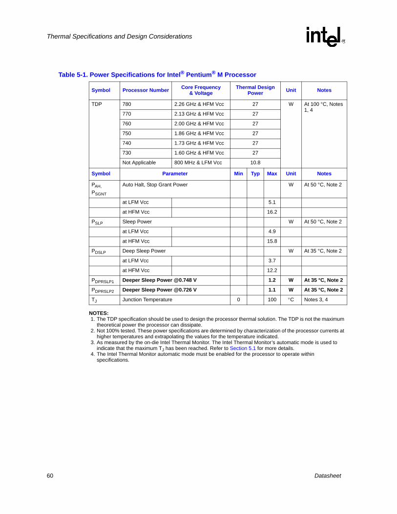
60 Datasheet
Thermal Specifications and Design Considerations
NOTES:1. The TDP specification should be used to design the processor thermal solution. The TDP is not the maximum
theoretical power the processor can dissipate. 2. Not 100% tested. These power specifications are determined by characterization of the processor currents at
higher temperatures and extrapolating the values for the temperature indicated.3. As measured by the on-die Intel Thermal Monitor. The Intel Thermal Monitor’s automatic mode is used to
indicate that the maximum TJ has been reached. Refer to Section 5.1 for more details.4. The Intel Thermal Monitor automatic mode must be enabled for the processor to operate within
specifications.
Table 5-1. Power Specifications for Intel® Pentium® M Processor
Symbol Processor Number Core Frequency & Voltage
Thermal Design Power Unit Notes
TDP 780 2.26 GHz & HFM Vcc 27 W At 100 °C, Notes 1, 4
770 2.13 GHz & HFM Vcc 27
760 2.00 GHz & HFM Vcc 27
750 1.86 GHz & HFM Vcc 27
740 1.73 GHz & HFM Vcc 27
730 1.60 GHz & HFM Vcc 27
Not Applicable 800 MHz & LFM Vcc 10.8
Symbol Parameter Min Typ Max Unit Notes
PAH,PSGNT
Auto Halt, Stop Grant Power W At 50 °C, Note 2
at LFM Vcc 5.1
at HFM Vcc 16.2
PSLP Sleep Power W At 50 °C, Note 2
at LFM Vcc 4.9
at HFM Vcc 15.8
PDSLP Deep Sleep Power W At 35 °C, Note 2
at LFM Vcc 3.7
at HFM Vcc 12.2
PDPRSLP1 Deeper Sleep Power @0.748 V 1.2 W At 35 °C, Note 2
PDPRSLP2 Deeper Sleep Power @0.726 V 1.1 W At 35 °C, Note 2
TJ Junction Temperature 0 100 °C Notes 3, 4
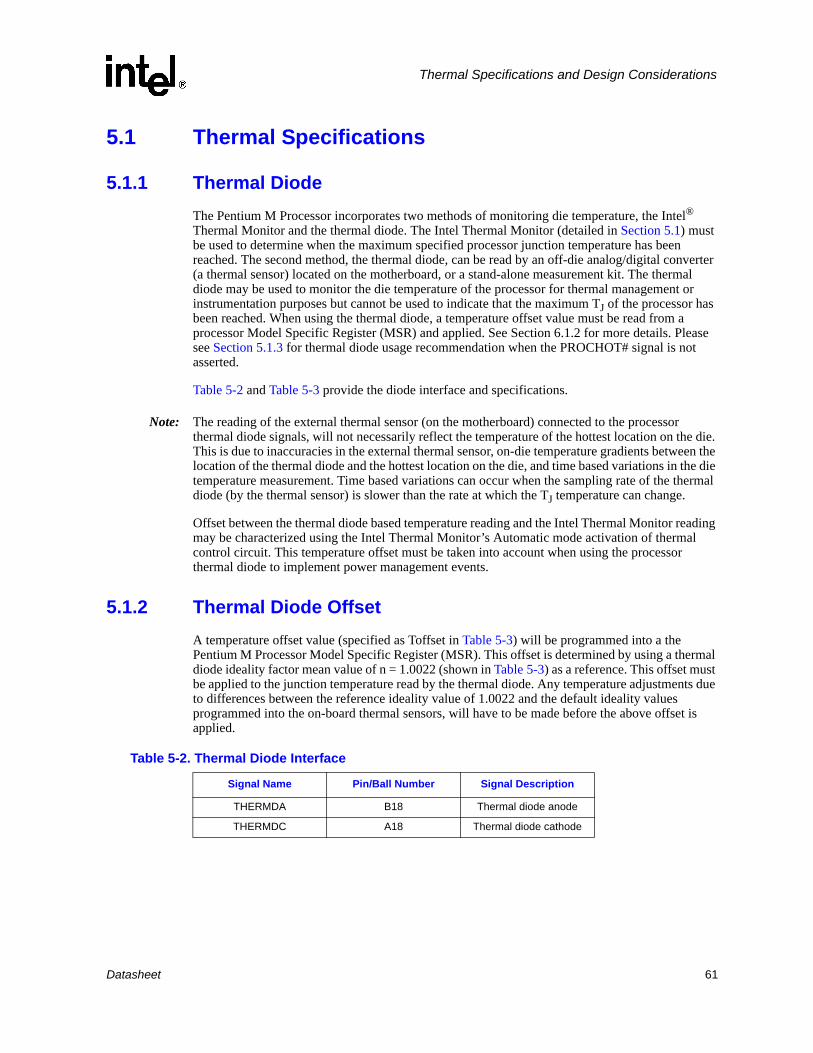
Datasheet 61
Thermal Specifications and Design Considerations
5.1 Thermal Specifications
5.1.1 Thermal DiodeThe Pentium M Processor incorporates two methods of monitoring die temperature, the Intel® Thermal Monitor and the thermal diode. The Intel Thermal Monitor (detailed in Section 5.1) must be used to determine when the maximum specified processor junction temperature has been reached. The second method, the thermal diode, can be read by an off-die analog/digital converter (a thermal sensor) located on the motherboard, or a stand-alone measurement kit. The thermal diode may be used to monitor the die temperature of the processor for thermal management or instrumentation purposes but cannot be used to indicate that the maximum TJ of the processor has been reached. When using the thermal diode, a temperature offset value must be read from a processor Model Specific Register (MSR) and applied. See Section 6.1.2 for more details. Please see Section 5.1.3 for thermal diode usage recommendation when the PROCHOT# signal is not asserted.
Table 5-2 and Table 5-3 provide the diode interface and specifications.
Note: The reading of the external thermal sensor (on the motherboard) connected to the processor thermal diode signals, will not necessarily reflect the temperature of the hottest location on the die. This is due to inaccuracies in the external thermal sensor, on-die temperature gradients between the location of the thermal diode and the hottest location on the die, and time based variations in the die temperature measurement. Time based variations can occur when the sampling rate of the thermal diode (by the thermal sensor) is slower than the rate at which the TJ temperature can change.
Offset between the thermal diode based temperature reading and the Intel Thermal Monitor reading may be characterized using the Intel Thermal Monitor’s Automatic mode activation of thermal control circuit. This temperature offset must be taken into account when using the processor thermal diode to implement power management events.
5.1.2 Thermal Diode OffsetA temperature offset value (specified as Toffset in Table 5-3) will be programmed into a the Pentium M Processor Model Specific Register (MSR). This offset is determined by using a thermal diode ideality factor mean value of n = 1.0022 (shown in Table 5-3) as a reference. This offset must be applied to the junction temperature read by the thermal diode. Any temperature adjustments due to differences between the reference ideality value of 1.0022 and the default ideality values programmed into the on-board thermal sensors, will have to be made before the above offset is applied.
Table 5-2. Thermal Diode Interface
Signal Name Pin/Ball Number Signal Description
THERMDA B18 Thermal diode anode
THERMDC A18 Thermal diode cathode
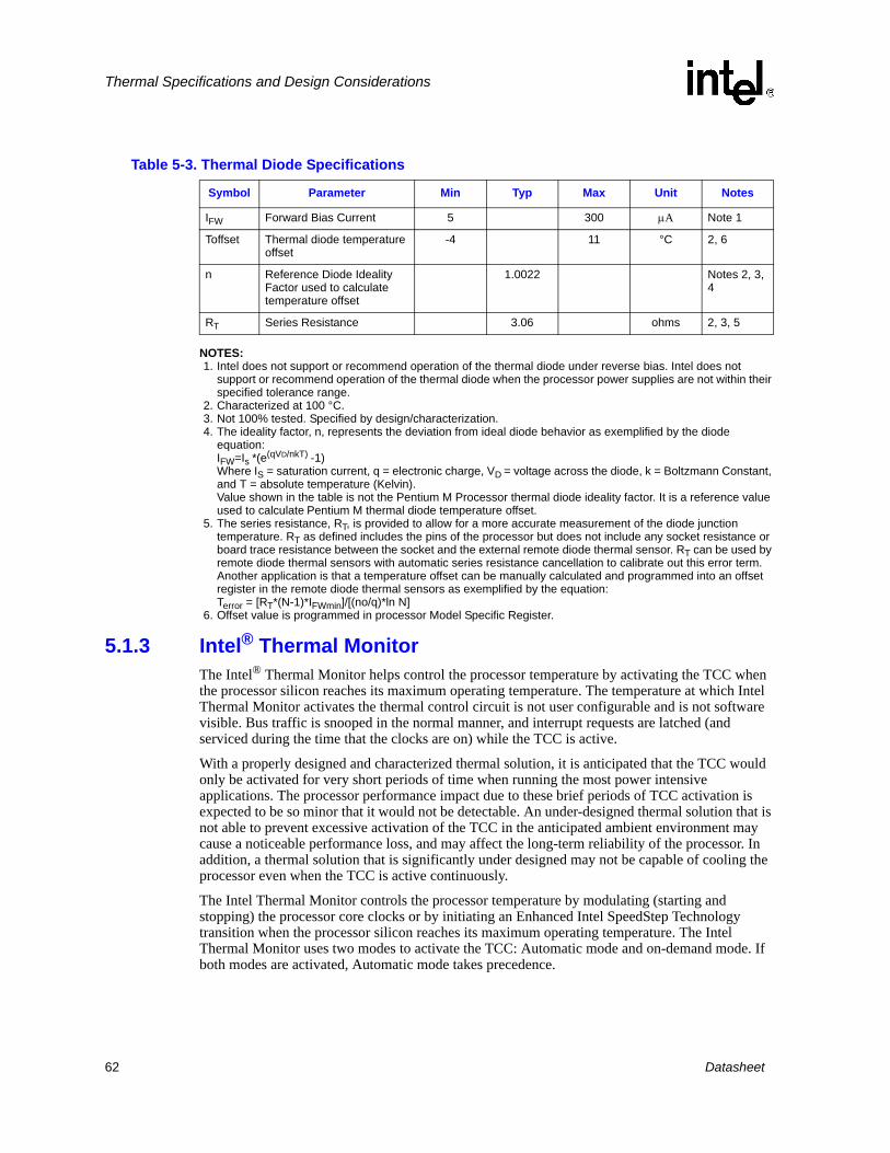
62 Datasheet
Thermal Specifications and Design Considerations
NOTES:1. Intel does not support or recommend operation of the thermal diode under reverse bias. Intel does not
support or recommend operation of the thermal diode when the processor power supplies are not within their specified tolerance range.
2. Characterized at 100 °C.3. Not 100% tested. Specified by design/characterization.4. The ideality factor, n, represents the deviation from ideal diode behavior as exemplified by the diode
equation: IFW=Is *(e(qVD/nkT) -1) Where IS = saturation current, q = electronic charge, VD = voltage across the diode, k = Boltzmann Constant, and T = absolute temperature (Kelvin).Value shown in the table is not the Pentium M Processor thermal diode ideality factor. It is a reference value used to calculate Pentium M thermal diode temperature offset.
5. The series resistance, RT, is provided to allow for a more accurate measurement of the diode junction temperature. RT as defined includes the pins of the processor but does not include any socket resistance or board trace resistance between the socket and the external remote diode thermal sensor. RT can be used by remote diode thermal sensors with automatic series resistance cancellation to calibrate out this error term. Another application is that a temperature offset can be manually calculated and programmed into an offset register in the remote diode thermal sensors as exemplified by the equation: Terror = [RT*(N-1)*IFWmin]/[(no/q)*ln N]
6. Offset value is programmed in processor Model Specific Register.
5.1.3 Intel® Thermal MonitorThe Intel® Thermal Monitor helps control the processor temperature by activating the TCC when the processor silicon reaches its maximum operating temperature. The temperature at which Intel Thermal Monitor activates the thermal control circuit is not user configurable and is not software visible. Bus traffic is snooped in the normal manner, and interrupt requests are latched (and serviced during the time that the clocks are on) while the TCC is active.
With a properly designed and characterized thermal solution, it is anticipated that the TCC would only be activated for very short periods of time when running the most power intensive applications. The processor performance impact due to these brief periods of TCC activation is expected to be so minor that it would not be detectable. An under-designed thermal solution that is not able to prevent excessive activation of the TCC in the anticipated ambient environment may cause a noticeable performance loss, and may affect the long-term reliability of the processor. In addition, a thermal solution that is significantly under designed may not be capable of cooling the processor even when the TCC is active continuously.
The Intel Thermal Monitor controls the processor temperature by modulating (starting and stopping) the processor core clocks or by initiating an Enhanced Intel SpeedStep Technology transition when the processor silicon reaches its maximum operating temperature. The Intel Thermal Monitor uses two modes to activate the TCC: Automatic mode and on-demand mode. If both modes are activated, Automatic mode takes precedence.
Table 5-3. Thermal Diode Specifications
Symbol Parameter Min Typ Max Unit Notes
IFW Forward Bias Current 5 300 µA Note 1
Toffset Thermal diode temperature offset
-4 11 °C 2, 6
n Reference Diode Ideality Factor used to calculate temperature offset
1.0022 Notes 2, 3, 4
RT Series Resistance 3.06 ohms 2, 3, 5

Datasheet 63
Thermal Specifications and Design Considerations
Note: The Intel Thermal Monitor automatic mode must be enabled through BIOS for the processor to be operating within specifications.
There are two automatic modes called Intel Thermal Monitor 1 and Intel Thermal Monitor 2. These modes are selected by writing values to the Model Specific Registers (MSRs) of the processor. After Automatic mode is enabled, the TCC will activate only when the internal die temperature reaches the maximum allowed value for operation.
Likewise, when Intel Thermal Monitor 2 is enabled, and a high temperature situation exists, the processor will perform an Enhanced Intel SpeedStep Technology transition to a lower operating point. When the processor temperature drops below the critical level, the processor will make an Enhanced Intel SpeedStep Technology transition to the last requested operating point. Intel Thermal Monitor 2 is the recommended mode on Pentium M Processors.
If a processor load based Enhanced Intel SpeedStep Technology transition (through MSR write) is initiated when an Intel Thermal Monitor 2 period is active, there are two possible results:
1.If the processor load based Enhanced Intel SpeedStep Technology transition target frequency is higher than the Intel Thermal Monitor 2 transition based target frequency, the processor load-based transition will be deferred until the Intel Thermal Monitor 2 event has been completed.
2.If the processor load-based Enhanced Intel SpeedStep Technology transition target frequency is lower than the Intel Thermal Monitor 2 transition based target frequency, the processor will transition to the processor load-based Enhanced Intel SpeedStep Technology target frequency point.
When Intel Thermal Monitor 1 is enabled, and a high temperature situation exists, the clocks will be modulated by alternately turning the clocks off and on at a 50% duty cycle. Cycle times are processor speed dependent and will decrease linearly as processor core frequencies increase. Once the temperature has returned to a non-critical level, modulation ceases and TCC goes inactive. A small amount of hysteresis has been included to prevent rapid active/inactive transitions of the TCC when the processor temperature is near the trip point. The duty cycle is factory configured and cannot be modified. Also, automatic mode does not require any additional hardware, software drivers, or interrupt handling routines. Processor performance will be decreased by the same amount as the duty cycle when the TCC is active, however, with a properly designed and characterized thermal solution the TCC most likely will never be activated, or only will be activated briefly during the most power intensive applications.
The TCC may also be activated via on-demand mode. If bit 4 of the ACPI Intel Thermal Monitor control register is written to a 1, the TCC will be activated immediately, independent of the processor temperature. When using on-demand mode to activate the TCC, the duty cycle of the clock modulation is programmable via bits 3:1 of the same ACPI Intel Thermal Monitor control register. In automatic mode, the duty cycle is fixed at 50% on, 50% off, however in on-demand mode, the duty cycle can be programmed from 12.5% on/ 87.5% off, to 87.5% on/12.5% off in 12.5% increments. On-demand mode may be used at the same time automatic mode is enabled, however, if the system tries to enable the TCC via on-demand mode at the same time automatic mode is enabled and a high temperature condition exists, automatic mode will take precedence.
An external signal, PROCHOT# (processor hot) is asserted when the processor detects that its temperature is above the thermal trip point. Bus snooping and interrupt latching are also active while the TCC is active.
64 Datasheet
Thermal Specifications and Design Considerations
Besides the thermal sensor and thermal control circuit, the Intel Thermal Monitor thermal monitor feature also includes one ACPI register, one performance counter register, three model specific registers (MSR), and one I/O pin (PROCHOT#). All are available to monitor and control the state of the Intel Thermal Monitor feature. The Intel Thermal Monitor can be configured to generate an interrupt upon the assertion or deassertion of PROCHOT#.
Note: PROCHOT# will not be asserted when the processor is in the Stop Grant, Sleep, Deep Sleep, and Deeper Sleep low power states (internal clocks stopped), hence the thermal diode reading must be used as a safeguard to maintain the processor junction temperature within the 100 °C (maximum) specification. If the platform thermal solution is not able to maintain the processor junction temperature within the maximum specification, the system must initiate an orderly shutdown to prevent damage. If the processor enters one of the above low power states with PROCHOT# already asserted, PROCHOT# will remain asserted until the processor exits the low power state and the processor junction temperature drops below the thermal trip point.
If automatic mode is disabled, the processor will be operating out of specification. Regardless of enabling the automatic or on-demand modes, in the event of a catastrophic cooling failure, the processor will automatically shut down when the silicon has reached a temperature of approximately 125 °C. At this point the THERMTRIP# signal will go active. THERMTRIP# activation is independent of processor activity and does not generate any bus cycles. When THERMTRIP# is asserted, the processor core voltage must be shut down within the time specified in Chapter 3.
§