Embed Size (px)
Citation preview
Intel® Cyclone® 10 GX Native FixedPoint DSP IP Core User Guide
SubscribeSend Feedback
UG-20094 | 2017.11.06Latest document on the web: PDF | HTML
Contents
1 Intel® Cyclone® 10 GX Native Fixed Point DSP IP Core User Guide.................................. 31.1 Cyclone 10 GX Native Fixed Point DSP IP Core Features............................................... 4
2 Getting Started................................................................................................................ 52.1 Cyclone 10 GX Native Fixed Point DSP IP Core Parameter Settings................................ 5
2.1.1 Operation Mode Tab.................................................................................... 52.1.2 Pre-adder Tab............................................................................................ 92.1.3 Internal Coefficient Tab................................................................................92.1.4 Accumulator/Output Cascade Tab................................................................102.1.5 Pipelining Tab........................................................................................... 122.1.6 Maximum Input Data Width Per Operation Mode............................................12
3 Functional Description................................................................................................... 143.1 Operational Modes................................................................................................ 14
3.1.1 The 18 × 18 Full Mode...............................................................................143.1.2 The 18 × 18 Sum of 2 Mode.......................................................................153.1.3 The 18 × 18 Plus 36 Mode......................................................................... 163.1.4 The 18 × 18 Systolic Mode.........................................................................183.1.5 The 27 × 27 Mode.................................................................................... 18
3.2 Optional Modules.................................................................................................. 193.2.1 Input Cascade.......................................................................................... 193.2.2 Pre-adder................................................................................................ 203.2.3 Internal Coefficient....................................................................................203.2.4 Accumulator and Output Cascade................................................................203.2.5 Pipeline Register....................................................................................... 21
3.3 Clocking Scheme.................................................................................................. 213.4 Cyclone 10 GX Native Fixed Point DSP IP Core Signals............................................... 22
A Document Revision History for the Cyclone 10 GX Native Fixed Point DSP IP CoreUser Guide...............................................................................................................26
Contents
Intel® Cyclone® 10 GX Native Fixed Point DSP IP Core User Guide2
1 Intel® Cyclone® 10 GX Native Fixed Point DSP IP CoreUser Guide
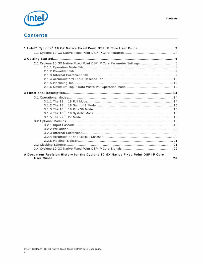
The Intel Cyclone® 10 GX Native Fixed Point DSP IP core instantiates and controls asingle Intel Cyclone 10 GX Variable Precision Digital Signal Processing (DSP) block.The Cyclone 10 GX Native Fixed Point DSP IP core is only available for Intel Cyclone 10GX devices.
Figure 1. Cyclone 10 GX Native Fixed Point DSP IP Core Functional Block Diagram
resultaresultb
+/-
chainin
chainout
ay
ax
sub
coefsela
ena aclr
clk
negate accumulate
loadconst
az
by
bx
coefselb
bz+/--
scanin
scanout
Pipeli
ne Re
giste
rsPip
eline
Regis
ters
Inpu
t Re
giste
rsIn
put R
egist
ers
TopMultiplier
Bottom Multiplier
x
x
InternalCoefficient
InternalCoefficient
OutputRegister
AdderChainadder
Double AccumulatorRegister
Top pre-adder
Bottom pre-adder
Bottom Delay
Register
TopDelay
Register
ChaininSystolicRegister
Input Systolic Register
++/-
+/-
Related Links
Introduction to Intel FPGA IP Cores
UG-20094 | 2017.11.06
Intel Corporation. All rights reserved. Intel, the Intel logo, Altera, Arria, Cyclone, Enpirion, MAX, Nios, Quartusand Stratix words and logos are trademarks of Intel Corporation or its subsidiaries in the U.S. and/or othercountries. Intel warrants performance of its FPGA and semiconductor products to current specifications inaccordance with Intel's standard warranty, but reserves the right to make changes to any products and servicesat any time without notice. Intel assumes no responsibility or liability arising out of the application or use of anyinformation, product, or service described herein except as expressly agreed to in writing by Intel. Intelcustomers are advised to obtain the latest version of device specifications before relying on any publishedinformation and before placing orders for products or services.*Other names and brands may be claimed as the property of others.
ISO9001:2008Registered
1.1 Cyclone 10 GX Native Fixed Point DSP IP Core Features
The Cyclone 10 GX Native Fixed Point DSP IP core supports the following features:
• High-performance, power-optimized, and fully registered multiplication operations
• 18-bit and 27-bit word lengths
• Two 18 × 19 multipliers or one 27 × 27 multiplier per DSP block
• Built-in addition, subtraction, and 64-bit double accumulation register to combinemultiplication results
• Cascading 19-bit or 27-bit when pre-adder is disabled and cascading 18-bit whenpre-adder is used to form the tap-delay line for filtering applications
• Cascading 64-bit output bus to propagate output results from one block to thenext block without external logic support
• Hard pre-adder supported in 19-bit and 27-bit modes for symmetric filters
• Internal coefficient register bank in both 18-bit and 27-bit modes for filterimplementation
• 18-bit and 27-bit systolic finite impulse response (FIR) filters with distributedoutput adder
1 Intel® Cyclone® 10 GX Native Fixed Point DSP IP Core User Guide
UG-20094 | 2017.11.06
Intel® Cyclone® 10 GX Native Fixed Point DSP IP Core User Guide4
2 Getting StartedThis chapter provides a general overview of the Intel FPGA IP core design flow to helpyou quickly get started with the Cyclone 10 GX Native Fixed Point DSP IP core. TheIntel FPGA IP Library is installed as part of the Intel Quartus® Prime installationprocess. You can select and parameterize any Intel FPGA IP core from the library. Intelprovides an integrated parameter editor that allows you to customize the Intel FPGADSP IP core to support a wide variety of applications. The parameter editor guides youthrough the setting of parameter values and selection of optional ports.
Related Links
• Introduction to Intel FPGA IP CoresProvides general information about all Intel FPGA IP cores, includingparameterizing, generating, upgrading, and simulating IP cores.
• Creating Version-Independent IP and Platform Designer (Standard) SimulationScripts
Create simulation scripts that do not require manual updates for software or IPversion upgrades.
• Project Management Best PracticesGuidelines for efficient management and portability of your project and IP files.
2.1 Cyclone 10 GX Native Fixed Point DSP IP Core ParameterSettings
You can customize the Cyclone 10 GX Native Fixed Point DSP IP core by specifying theparameters using the parameter editor in the Intel Quartus Prime software.
2.1.1 Operation Mode Tab
Table 1. Operation Mode Tab
Parameter IP GeneratedParameter
Value Description
Please choose theoperation mode
operation_mode m18×18_fullm18×18_sumof2m18×18_plus36m18×18_systolicm27×27
Select the desiredoperational mode.
Multiplier Configuration
Representation formatfor top multiplier xoperand
signed_max signedunsigned
Specify therepresentation formatfor the top multiplierx operand.
continued...
UG-20094 | 2017.11.06
Intel Corporation. All rights reserved. Intel, the Intel logo, Altera, Arria, Cyclone, Enpirion, MAX, Nios, Quartusand Stratix words and logos are trademarks of Intel Corporation or its subsidiaries in the U.S. and/or othercountries. Intel warrants performance of its FPGA and semiconductor products to current specifications inaccordance with Intel's standard warranty, but reserves the right to make changes to any products and servicesat any time without notice. Intel assumes no responsibility or liability arising out of the application or use of anyinformation, product, or service described herein except as expressly agreed to in writing by Intel. Intelcustomers are advised to obtain the latest version of device specifications before relying on any publishedinformation and before placing orders for products or services.*Other names and brands may be claimed as the property of others.
ISO9001:2008Registered
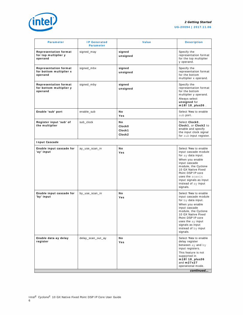
Parameter IP GeneratedParameter
Value Description
Representation formatfor top multiplier yoperand
signed_may signedunsigned
Specify therepresentation formatfor the top multipliery operand.
Representation formatfor bottom multiplier xoperand
signed_mbx signedunsigned
Specify therepresentation formatfor the bottommultiplier x operand.
Representation formatfor bottom multiplier yoperand
signed_mby signedunsigned
Specify therepresentation formatfor the bottommultiplier y operand.Always selectunsigned form18×18_plus36 .
Enable 'sub' port enable_sub NoYes
Select Yes to enablesub port.
Register input 'sub' ofthe multiplier
sub_clock NoClock0Clock1Clock2
Select Clock0,Clock1, or Clock2 toenable and specifythe input clock signalfor sub input register.
Input Cascade
Enable input cascade for'ay' input
ay_use_scan_in NoYes
Select Yes to enableinput cascade modulefor ay data input.When you enableinput cascademodule, the Cyclone10 GX Native FixedPoint DSP IP coreuses the scanininput signals as inputinstead of ay inputsignals.
Enable input cascade for'by' input
by_use_scan_in NoYes
Select Yes to enableinput cascade modulefor by data input.When you enableinput cascademodule, the Cyclone10 GX Native FixedPoint DSP IP coreuses the ay inputsignals as inputinstead of by inputsignals.
Enable data ay delayregister
delay_scan_out_ay NoYes
Select Yes to enabledelay registerbetween ay and byinput registers.This feature is notsupported inm18×18_plus36and m27x27operational mode.
continued...
2 Getting Started
UG-20094 | 2017.11.06
Intel® Cyclone® 10 GX Native Fixed Point DSP IP Core User Guide6
Parameter IP GeneratedParameter
Value Description
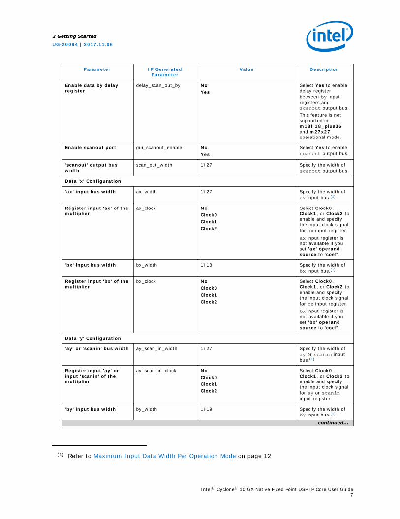
Enable data by delayregister
delay_scan_out_by NoYes
Select Yes to enabledelay registerbetween by inputregisters andscanout output bus.This feature is notsupported inm18×18_plus36and m27x27operational mode.
Enable scanout port gui_scanout_enable NoYes
Select Yes to enablescanout output bus.
'scanout' output buswidth
scan_out_width 1–27 Specify the width ofscanout output bus.
Data 'x' Configuration
'ax' input bus width ax_width 1–27 Specify the width ofax input bus.(1)
Register input 'ax' of themultiplier
ax_clock NoClock0Clock1Clock2
Select Clock0,Clock1, or Clock2 toenable and specifythe input clock signalfor ax input register.ax input register isnot available if youset 'ax' operandsource to 'coef'.
'bx' input bus width bx_width 1–18 Specify the width ofbx input bus.(1)
Register input 'bx' of themultiplier
bx_clock NoClock0Clock1Clock2
Select Clock0,Clock1, or Clock2 toenable and specifythe input clock signalfor bx input register.bx input register isnot available if youset 'bx' operandsource to 'coef'.
Data 'y' Configuration
'ay' or 'scanin' bus width ay_scan_in_width 1–27 Specify the width ofay or scanin inputbus.(1)
Register input 'ay' orinput 'scanin' of themultiplier
ay_scan_in_clock NoClock0Clock1Clock2
Select Clock0,Clock1, or Clock2 toenable and specifythe input clock signalfor ay or scanininput register.
'by' input bus width by_width 1–19 Specify the width ofby input bus.(1)
continued...
(1) Refer to Maximum Input Data Width Per Operation Mode on page 12
2 Getting Started
UG-20094 | 2017.11.06
Intel® Cyclone® 10 GX Native Fixed Point DSP IP Core User Guide7
Parameter IP GeneratedParameter
Value Description
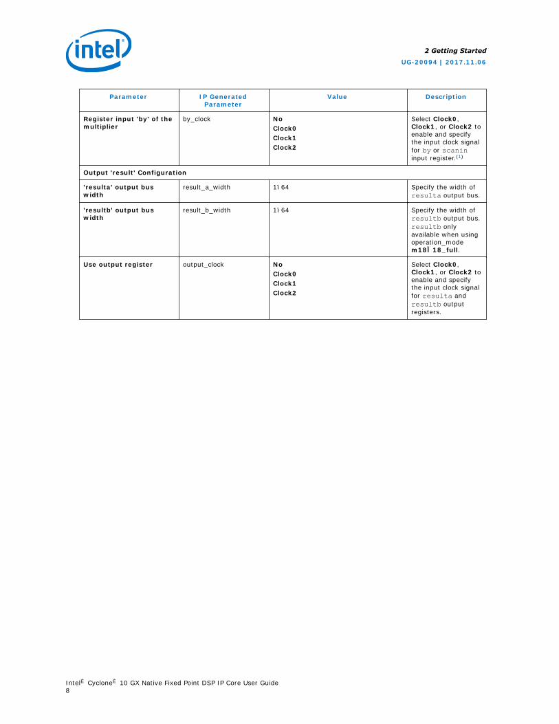
Register input 'by' of themultiplier
by_clock NoClock0Clock1Clock2
Select Clock0,Clock1, or Clock2 toenable and specifythe input clock signalfor by or scanininput register.(1)
Output 'result' Configuration
'resulta' output buswidth
result_a_width 1–64 Specify the width ofresulta output bus.
'resultb' output buswidth
result_b_width 1–64 Specify the width ofresultb output bus.resultb onlyavailable when usingoperation_modem18×18_full.
Use output register output_clock NoClock0Clock1Clock2
Select Clock0,Clock1, or Clock2 toenable and specifythe input clock signalfor resulta andresultb outputregisters.
2 Getting Started
UG-20094 | 2017.11.06
Intel® Cyclone® 10 GX Native Fixed Point DSP IP Core User Guide8
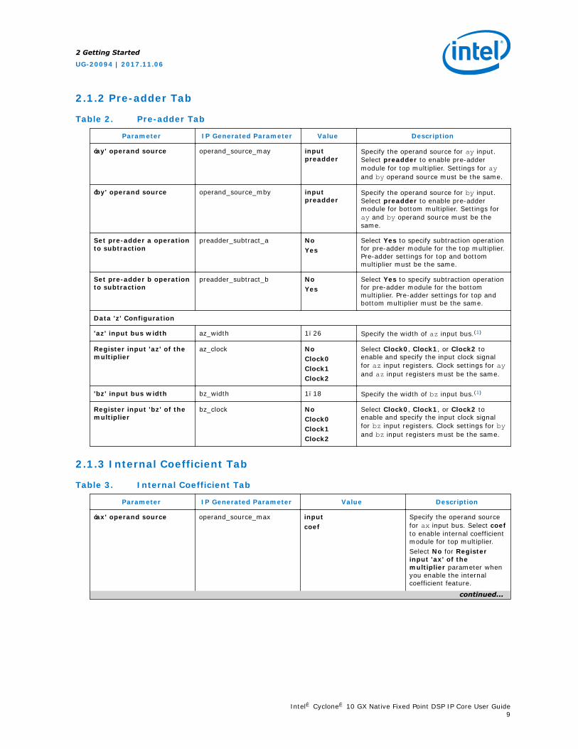
2.1.2 Pre-adder Tab
Table 2. Pre-adder Tab
Parameter IP Generated Parameter Value Description
‘ay' operand source operand_source_may inputpreadder
Specify the operand source for ay input.Select preadder to enable pre-addermodule for top multiplier. Settings for ayand by operand source must be the same.
‘by' operand source operand_source_mby inputpreadder
Specify the operand source for by input.Select preadder to enable pre-addermodule for bottom multiplier. Settings foray and by operand source must be thesame.
Set pre-adder a operationto subtraction
preadder_subtract_a NoYes
Select Yes to specify subtraction operationfor pre-adder module for the top multiplier.Pre-adder settings for top and bottommultiplier must be the same.
Set pre-adder b operationto subtraction
preadder_subtract_b NoYes
Select Yes to specify subtraction operationfor pre-adder module for the bottommultiplier. Pre-adder settings for top andbottom multiplier must be the same.
Data 'z' Configuration
'az' input bus width az_width 1–26 Specify the width of az input bus.(1)
Register input 'az' of themultiplier
az_clock NoClock0Clock1Clock2
Select Clock0, Clock1, or Clock2 toenable and specify the input clock signalfor az input registers. Clock settings for ayand az input registers must be the same.
'bz' input bus width bz_width 1–18 Specify the width of bz input bus.(1)
Register input 'bz' of themultiplier
bz_clock NoClock0Clock1Clock2
Select Clock0, Clock1, or Clock2 toenable and specify the input clock signalfor bz input registers. Clock settings for byand bz input registers must be the same.
2.1.3 Internal Coefficient Tab
Table 3. Internal Coefficient Tab
Parameter IP Generated Parameter Value Description
‘ax' operand source operand_source_max inputcoef
Specify the operand sourcefor ax input bus. Select coefto enable internal coefficientmodule for top multiplier.Select No for Registerinput 'ax' of themultiplier parameter whenyou enable the internalcoefficient feature.
continued...
2 Getting Started
UG-20094 | 2017.11.06
Intel® Cyclone® 10 GX Native Fixed Point DSP IP Core User Guide9
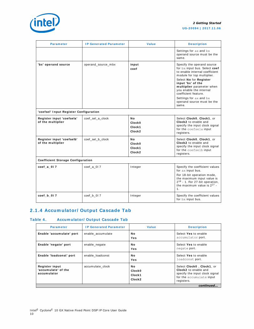
Parameter IP Generated Parameter Value Description
Settings for ax and bxoperand source must be thesame.
'bx' operand source operand_source_mbx inputcoef
Specify the operand sourcefor bx input bus. Select coefto enable internal coefficientmodule for top multiplier.Select No for Registerinput 'bx' of themultiplier parameter whenyou enable the internalcoefficient feature.Settings for ax and bxoperand source must be thesame.
'coefsel' Input Register Configuration
Register input 'coefsela'of the multiplier
coef_sel_a_clock NoClock0Clock1Clock2
Select Clock0, Clock1, orClock2 to enable andspecify the input clock signalfor the coefsela inputregisters.
Register input 'coefselb'of the multiplier
coef_sel_b_clock NoClock0Clock1Clock2
Select Clock0, Clock1, orClock2 to enable andspecify the input clock signalfor the coefselb inputregisters.
Coefficient Storage Configuration
coef_a_0–7 coef_a_0–7 Integer Specify the coefficient valuesfor ax input bus.For 18-bit operation mode,the maximum input value is218 - 1. For 27-bit operation,the maximum value is 227 -1.
coef_b_0–7 coef_b_0–7 Integer Specify the coefficient valuesfor bx input bus.
2.1.4 Accumulator/Output Cascade Tab
Table 4. Accumulator/Output Cascade Tab
Parameter IP Generated Parameter Value Description
Enable 'accumulate' port enable_accumulate NoYes
Select Yes to enableaccumulator port.
Enable 'negate' port enable_negate NoYes
Select Yes to enablenegate port.
Enable 'loadconst' port enable_loadconst NoYes
Select Yes to enableloadconst port.
Register input'accumulate' of theaccumulator
accumulate_clock NoClock0Clock1Clock2
Select Clock0 , Clock1, orClock2 to enable andspecify the input clock signalfor the accumulate inputregisters.
continued...
2 Getting Started
UG-20094 | 2017.11.06
Intel® Cyclone® 10 GX Native Fixed Point DSP IP Core User Guide10
Parameter IP Generated Parameter Value Description
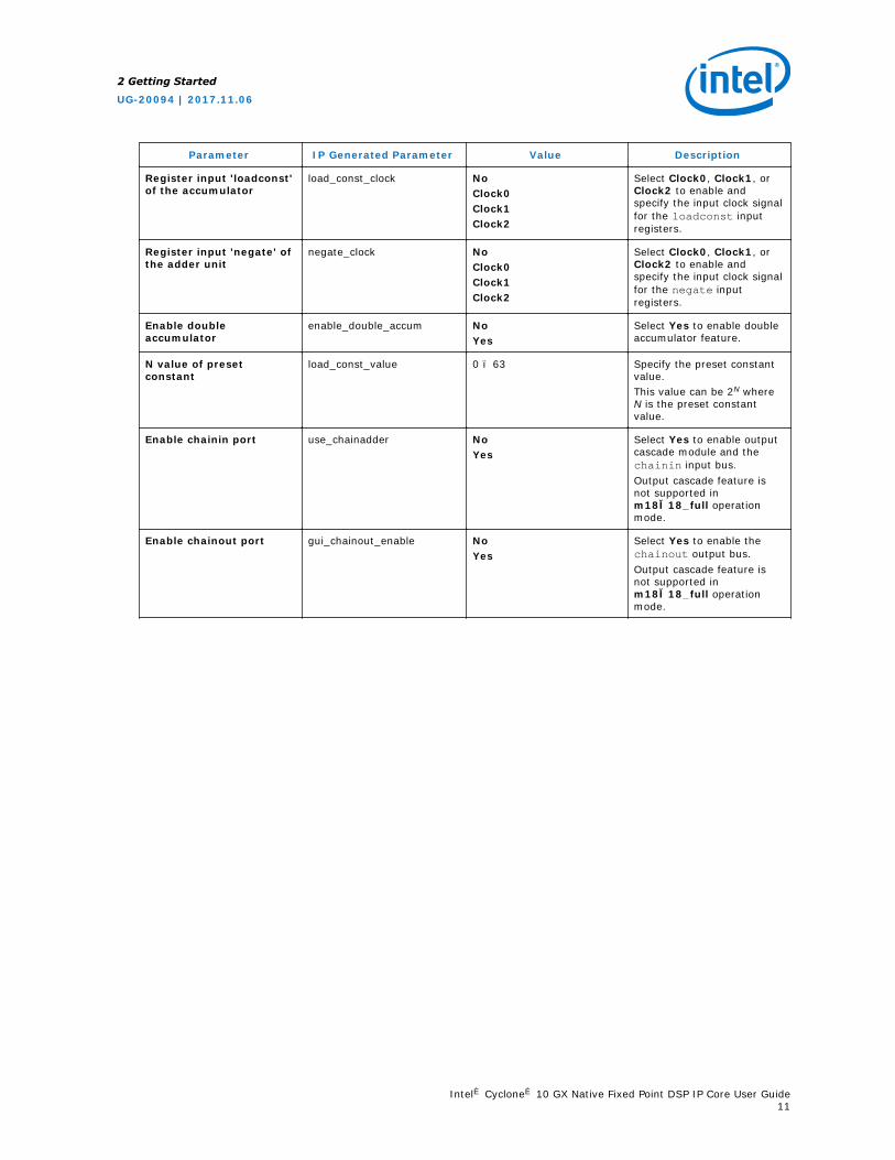
Register input 'loadconst'of the accumulator
load_const_clock NoClock0Clock1Clock2
Select Clock0, Clock1, orClock2 to enable andspecify the input clock signalfor the loadconst inputregisters.
Register input 'negate' ofthe adder unit
negate_clock NoClock0Clock1Clock2
Select Clock0, Clock1, orClock2 to enable andspecify the input clock signalfor the negate inputregisters.
Enable doubleaccumulator
enable_double_accum NoYes
Select Yes to enable doubleaccumulator feature.
N value of presetconstant
load_const_value 0 – 63 Specify the preset constantvalue.This value can be 2N whereN is the preset constantvalue.
Enable chainin port use_chainadder NoYes
Select Yes to enable outputcascade module and thechainin input bus.Output cascade feature isnot supported inm18×18_full operationmode.
Enable chainout port gui_chainout_enable NoYes
Select Yes to enable thechainout output bus.Output cascade feature isnot supported inm18×18_full operationmode.
2 Getting Started
UG-20094 | 2017.11.06
Intel® Cyclone® 10 GX Native Fixed Point DSP IP Core User Guide11
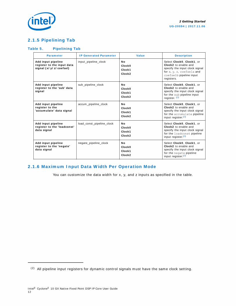
2.1.5 Pipelining Tab
Table 5. Pipelining Tab
Parameter IP Generated Parameter Value Description
Add input pipelineregister to the input datasignal (x/y/z/coefsel)
input_pipeline_clock NoClock0Clock1Clock2
Select Clock0, Clock1, orClock2 to enable andspecify the input clock signalfor x, y, z, coefsela andcoefselb pipeline inputregisters.
Add input pipelineregister to the 'sub' datasignal
sub_pipeline_clock NoClock0Clock1Clock2
Select Clock0, Clock1, orClock2 to enable andspecify the input clock signalfor the sub pipeline inputregister. (2)
Add input pipelineregister to the'accumulate' data signal
accum_pipeline_clock NoClock0Clock1Clock2
Select Clock0, Clock1, orClock2 to enable andspecify the input clock signalfor the accumulate pipelineinput register.(2)
Add input pipelineregister to the 'loadconst'data signal
load_const_pipeline_clock NoClock0Clock1Clock2
Select Clock0, Clock1, orClock2 to enable andspecify the input clock signalfor the loadconst pipelineinput register.(2)
Add input pipelineregister to the 'negate'data signal
negate_pipeline_clock NoClock0Clock1Clock2
Select Clock0, Clock1, orClock2 to enable andspecify the input clock signalfor the negate pipelineinput register.(2)
2.1.6 Maximum Input Data Width Per Operation Mode
You can customize the data width for x, y, and z inputs as specified in the table.
(2) All pipeline input registers for dynamic control signals must have the same clock setting.
2 Getting Started
UG-20094 | 2017.11.06
Intel® Cyclone® 10 GX Native Fixed Point DSP IP Core User Guide12
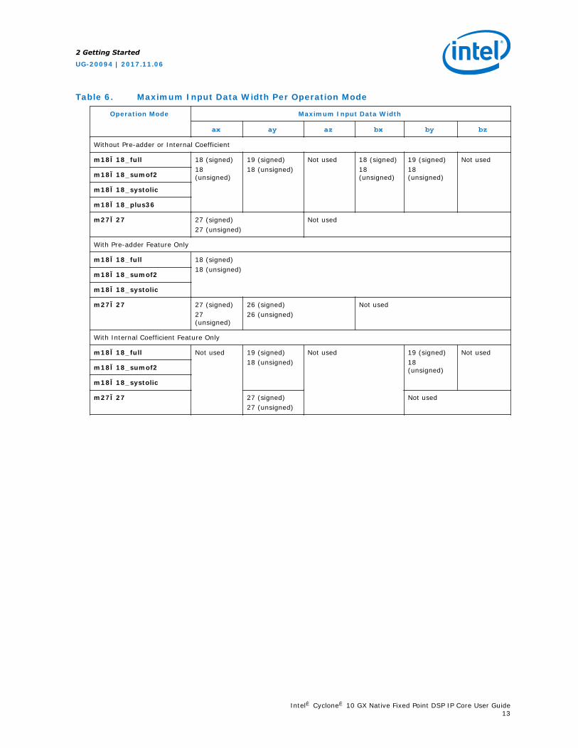
Table 6. Maximum Input Data Width Per Operation Mode
Operation Mode Maximum Input Data Width
ax ay az bx by bz
Without Pre-adder or Internal Coefficient
m18×18_full 18 (signed)18(unsigned)
19 (signed)18 (unsigned)
Not used 18 (signed)18(unsigned)
19 (signed)18(unsigned)
Not used
m18×18_sumof2
m18×18_systolic
m18×18_plus36
m27×27 27 (signed)27 (unsigned)
Not used
With Pre-adder Feature Only
m18×18_full 18 (signed)18 (unsigned)
m18×18_sumof2
m18×18_systolic
m27×27 27 (signed)27(unsigned)
26 (signed)26 (unsigned)
Not used
With Internal Coefficient Feature Only
m18×18_full Not used 19 (signed)18 (unsigned)
Not used 19 (signed)18(unsigned)
Not used
m18×18_sumof2
m18×18_systolic
m27×27 27 (signed)27 (unsigned)
Not used
2 Getting Started
UG-20094 | 2017.11.06
Intel® Cyclone® 10 GX Native Fixed Point DSP IP Core User Guide13
3 Functional Description
The Cyclone 10 GX Native Fixed Point DSP IP core consists of 2 architectures; 18 × 18multiplication and 27 × 27 multiplication. Each instantiation of the Cyclone 10 GXNative Fixed Point DSP IP core generates only 1 of the 2 architectures depending onthe selected operational modes. You can enable optional modules to your application.
Related Links
Variable Precision DSP Blocks in Intel Cyclone 10 GX Devices chapter,Intel Cyclone 10 GX Core Fabric and General Purpose I/Os Handbook
3.1 Operational Modes
The Cyclone 10 GX Native Fixed Point DSP IP core supports 5 operational modes:
• The 18 × 18 Full Mode
• The 18 × 18 Sum of 2 Mode
• The 18 × 18 Plus 36 Mode
• The 18 × 18 Systolic Mode
• The 27 × 27 Mode
3.1.1 The 18 × 18 Full Mode
When configured as 18 × 18 full mode, the Cyclone 10 GX Native Fixed Point DSP IPcore operates as two independent 18 (signed / unsigned) × 19 (signed) or 18(signed / unsigned) × 18 (unsigned) multipliers with 37-bit output. This mode appliesthe following equations:
• resulta = ax * ay
• resultb = bx * by
UG-20094 | 2017.11.06
Intel Corporation. All rights reserved. Intel, the Intel logo, Altera, Arria, Cyclone, Enpirion, MAX, Nios, Quartusand Stratix words and logos are trademarks of Intel Corporation or its subsidiaries in the U.S. and/or othercountries. Intel warrants performance of its FPGA and semiconductor products to current specifications inaccordance with Intel's standard warranty, but reserves the right to make changes to any products and servicesat any time without notice. Intel assumes no responsibility or liability arising out of the application or use of anyinformation, product, or service described herein except as expressly agreed to in writing by Intel. Intelcustomers are advised to obtain the latest version of device specifications before relying on any publishedinformation and before placing orders for products or services.*Other names and brands may be claimed as the property of others.
ISO9001:2008Registered
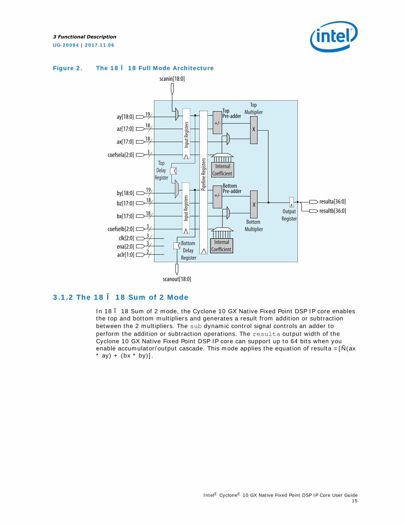
Figure 2. The 18 × 18 Full Mode Architecture
resulta[36:0]resultb[36:0]
ay[18:0]
ax[17:0]
coefsela[2:0]
ena[2:0] aclr[1:0]
clk[2:0]
az[17:0]+/-
by[18:0]
bx[17:0]
coefselb[2:0]
bz[17:0]
scanin[18:0]
scanout[18:0]
Pipeli
ne Re
giste
rs
Inpu
t Reg
ister
s
TopMultiplier
Bottom Multiplier
x
x
InternalCoefficient
InternalCoefficient
OutputRegister
Top Pre-adder
Bottom Pre-adder
Bottom Delay
Register
19
18
18
3
19
18
18
3
332
Inpu
t Reg
ister
s +/-
TopDelay
Register
3.1.2 The 18 × 18 Sum of 2 Mode
In 18 × 18 Sum of 2 mode, the Cyclone 10 GX Native Fixed Point DSP IP core enablesthe top and bottom multipliers and generates a result from addition or subtractionbetween the 2 multipliers. The sub dynamic control signal controls an adder toperform the addition or subtraction operations. The resulta output width of theCyclone 10 GX Native Fixed Point DSP IP core can support up to 64 bits when youenable accumulator/output cascade. This mode applies the equation of resulta =[±(ax* ay) + (bx * by)].
3 Functional Description
UG-20094 | 2017.11.06
Intel® Cyclone® 10 GX Native Fixed Point DSP IP Core User Guide15
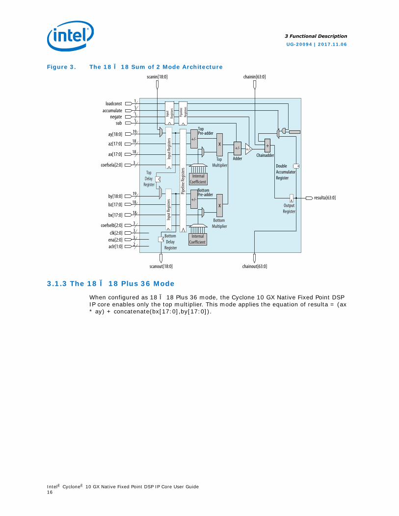
Figure 3. The 18 × 18 Sum of 2 Mode Architecture
resulta[63:0]
+/- ++/-
chainin[63:0]
chainout[63:0]
ay[18:0]
ax[17:0]
sub
coefsela[2:0]
ena[2:0] aclr[1:0]
clk[2:0]
negate accumulate
loadconst
az[17:0]+/-
by[18:0]
bx[17:0]
coefselb[2:0]
bz[17:0]+/-
scanin[18:0]
scanout[18:0]
Pipeli
ne Re
giste
rsPip
eline
Regis
ters
Inpu
t Re
giste
rsIn
put R
egist
ers
Top Multiplier
Bottom Multiplier
x
x
InternalCoefficient
OutputRegister
AdderChainadder
Double AccumulatorRegister
Top Pre-adder
Bottom Pre-adder
Bottom Delay
Register
1111
19
18
18
3
19
18
18
3
332
Inpu
t Reg
ister
sTop
Delay Register
InternalCoefficient
3.1.3 The 18 × 18 Plus 36 Mode
When configured as 18 × 18 Plus 36 mode, the Cyclone 10 GX Native Fixed Point DSPIP core enables only the top multiplier. This mode applies the equation of resulta = (ax* ay) + concatenate(bx[17:0],by[17:0]).
3 Functional Description
UG-20094 | 2017.11.06
Intel® Cyclone® 10 GX Native Fixed Point DSP IP Core User Guide16
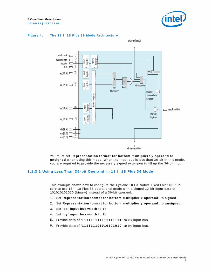
Figure 4. The 18 × 18 Plus 36 Mode Architecture
resulta[63:0]
+/-++/-
chainin[63:0]
chainout[63:0]
ay[18:0]
ax[17:0]
sub
ena[2:0] aclr[1:0]
clk[2:0]
negate accumulate
loadconst
by[17:0]
bx[17:0]
Pipeli
ne Re
giste
rs
Inpu
t Re
giste
rsTop
Multiplier
x
OutputRegister
Adder Chainadder
Double AccumulatorRegister
1111
19
18
18
18
332
Inpu
tRe
giste
rsIn
put
Regis
ters
Inpu
tRe
giste
rsIn
put
Regis
ters
Pipeli
neRe
giste
rs
You must set Representation format for bottom multipliers y operand tounsigned when using this mode. When the input bus is less than 36-bit in this mode,you are required to provide the necessary signed extension to fill up the 36-bit input.
3.1.3.1 Using Less Than 36-bit Operand In 18 × 18 Plus 36 Mode
This example shows how to configure the Cyclone 10 GX Native Fixed Point DSP IPcore to use 18 × 18 Plus 36 operational mode with a signed 12-bit input data of101010101010 (binary) instead of a 36-bit operand.
1. Set Representation format for bottom multiplier x operand: to signed.
2. Set Representation format for bottom multiplier y operand: to unsigned.
3. Set 'bx' input bus width to 18.
4. Set 'by' input bus width to 18.
5. Provide data of '111111111111111111' to bx input bus.
6. Provide data of '111111101010101010' to by input bus.
3 Functional Description
UG-20094 | 2017.11.06
Intel® Cyclone® 10 GX Native Fixed Point DSP IP Core User Guide17
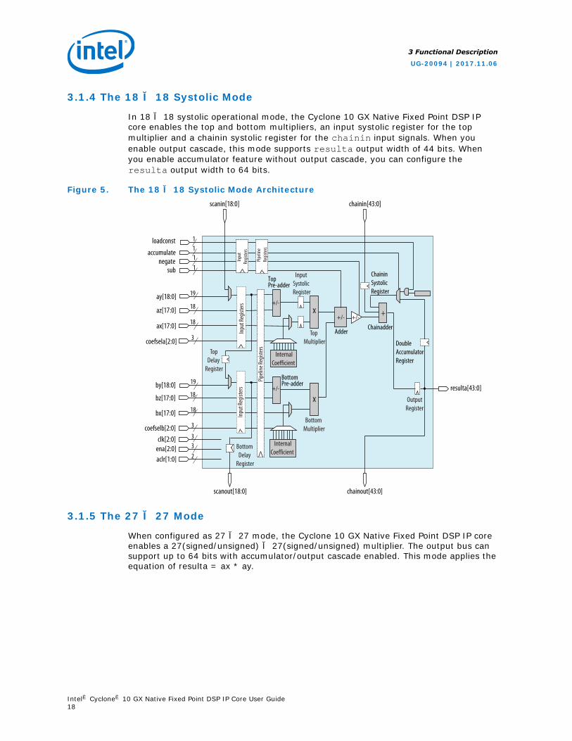
3.1.4 The 18 × 18 Systolic Mode
In 18 × 18 systolic operational mode, the Cyclone 10 GX Native Fixed Point DSP IPcore enables the top and bottom multipliers, an input systolic register for the topmultiplier and a chainin systolic register for the chainin input signals. When youenable output cascade, this mode supports resulta output width of 44 bits. Whenyou enable accumulator feature without output cascade, you can configure theresulta output width to 64 bits.
Figure 5. The 18 × 18 Systolic Mode Architecture
resulta[43:0]
+/-+
+/-
chainin[43:0]
chainout[43:0]
ay[18:0]
ax[17:0]
sub
ena[2:0] aclr[1:0]
clk[2:0]
negate accumulate
loadconst
az[17:0]
by[18:0]
bx[17:0]
coefselb[2:0]
bz[17:0]
scanin[18:0]
scanout[18:0]
Pipeli
ne Re
giste
rsPip
eline
Regis
ters
Inpu
t Re
giste
rsIn
put R
egist
ers
Top Multiplier
Bottom Multiplier
x
x
InternalCoefficient
InternalCoefficient
OutputRegister
AdderChainadder
Double AccumulatorRegister
Top Pre-adder
Bottom Pre-adder
Bottom Delay
Register
TopDelay
Register
ChaininSystolicRegister
1111
19
18
18
3
19
18
18
3
332
Input Systolic Register
Inpu
t Reg
ister
s
+/-
+/-
coefsela[2:0]
3.1.5 The 27 × 27 Mode
When configured as 27 × 27 mode, the Cyclone 10 GX Native Fixed Point DSP IP coreenables a 27(signed/unsigned) × 27(signed/unsigned) multiplier. The output bus cansupport up to 64 bits with accumulator/output cascade enabled. This mode applies theequation of resulta = ax * ay.
3 Functional Description
UG-20094 | 2017.11.06
Intel® Cyclone® 10 GX Native Fixed Point DSP IP Core User Guide18
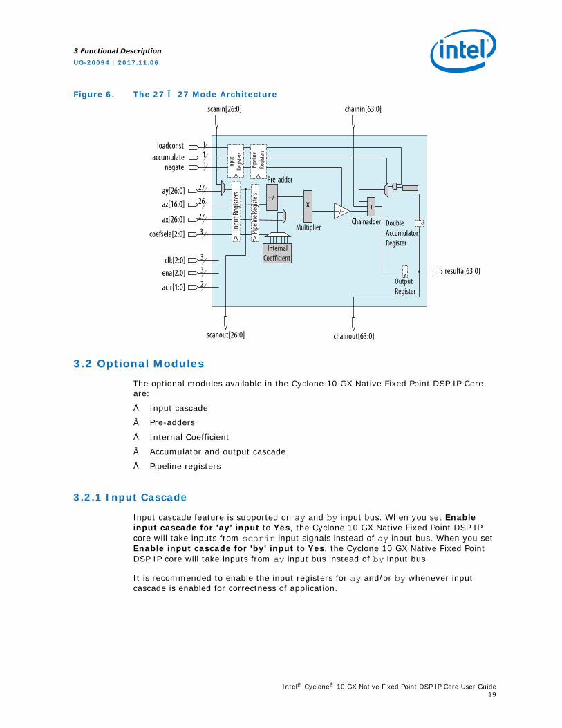
Figure 6. The 27 × 27 Mode Architecture
resulta[63:0]
++/-
chainin[63:0]
chainout[63:0]
ay[26:0]
ax[26:0]
coefsela[2:0]
ena[2:0]
aclr[1:0]
clk[2:0]
negate accumulate
loadconst
az[16:0]+/-
scanin[26:0]
scanout[26:0]
Pipeli
ne Re
giste
rsPip
eline
Regis
ters
Inpu
t Re
giste
rsIn
put R
egist
ers
Multiplier
x
InternalCoefficient
OutputRegister
Chainadder Double AccumulatorRegister
Pre-adder
111
27
26
27
3
3
3
2
3.2 Optional Modules
The optional modules available in the Cyclone 10 GX Native Fixed Point DSP IP Coreare:
• Input cascade
• Pre-adders
• Internal Coefficient
• Accumulator and output cascade
• Pipeline registers
3.2.1 Input Cascade
Input cascade feature is supported on ay and by input bus. When you set Enableinput cascade for 'ay' input to Yes, the Cyclone 10 GX Native Fixed Point DSP IPcore will take inputs from scanin input signals instead of ay input bus. When you setEnable input cascade for 'by' input to Yes, the Cyclone 10 GX Native Fixed PointDSP IP core will take inputs from ay input bus instead of by input bus.
It is recommended to enable the input registers for ay and/or by whenever inputcascade is enabled for correctness of application.
3 Functional Description
UG-20094 | 2017.11.06
Intel® Cyclone® 10 GX Native Fixed Point DSP IP Core User Guide19
You can enable the delay registers to match the latency requirement between theinput register and the output register. There are 2 delay registers in the core. The topdelay register is used for ay or scanin input ports while the bottom delay register isused for scanout output ports. These delay registers are supported in 18 × 18 fullmode, 18 × 18 sum of 2 mode, and 18 × 18 systolic mode.
3.2.2 Pre-adder
The pre-adder can be configured in the following configurations:
• Two independent 18-bit (signed/unsigned) pre-adders.
• One 26-bit pre-adder.
When you enable pre-adder in 18 × 18 multiplication modes, ay and az are used asthe input bus to the top pre-adder while by and bz are used as the input bus to thebottom pre-adder. When you enable pre-adder in 27 × 27 multiplication mode, ay andaz are used as the input bus to the pre-adder.
The pre-adder supports both addition and subtraction operations. When both pre-adders within the same DSP block are used, they must share the same operation type(either addition or subtraction).
3.2.3 Internal Coefficient
The internal coefficient can support up to eight constant coefficients for themultiplicands in 18-bit and 27-bit modes. When you enable the internal coefficientfeature, two input bus to control the selection of the coefficient multiplexer will begenerated. The coefsela input bus is used to select the predefined coefficients fortop multiplier and coefselb input bus is used to select the predefined coefficients forbottom multiplier.
The internal coefficient storage does not support dynamically controllable coefficientvalues and external coefficient storage is required to perform such operation.
3.2.4 Accumulator and Output Cascade
The accumulator module can be enabled to perform the following operations:
• Addition or subtraction operation
• Biased rounding operation using a constant value of 2N
• Dual channel accumulation
To dynamically perform addition or subtraction operation of the accumulator, controlthe negate input signal.
For biased rounding operation, you can specify and load a preset constant of 2N beforethe accumulator module is enabled by specifying an integer to the parameter N valueof preset constant. The integer N must be less than 64. You can dynamically enableor disable the use of the preset constant by controlling the loadconst signal. You canuse this operation as an active muxing of the round value into the accumulatorfeedback path. The loadconst and the accumulate signals usage is mutuallyexclusive.
3 Functional Description
UG-20094 | 2017.11.06
Intel® Cyclone® 10 GX Native Fixed Point DSP IP Core User Guide20
You can enable the double accumulator register using the parameter Enable doubleaccumulator to perform double accumulation.
The accumulator module can support chaining of multiple DSP blocks for addition orsubtraction operation by enabling chainin input port and chainout output port. In18 × 18 systolic mode, only 44-bit of the chainin input bus and chainout outputbus will be used. However, all 64-bit chainin input bus must be connected to thechainout output bus from the preceding DSP block.
3.2.5 Pipeline Register
The Cyclone 10 GX Native Fixed Point DSP IP core supports a single level of pipelineregister. The pipeline register supports up to three clock sources and oneasynchronous clear signal to reset the pipeline registers. There are five pipelineregisters:
• data input bus pipeline register
• sub dynamic control signal pipeline register
• negate dynamic control signal pipeline register
• accumulate dynamic control signal pipeline register
• loadconst dynamic control pipeline register
You can choose to enable each data input bus pipeline registers and the dynamiccontrol signal pipeline registers independently. However, all enabled pipeline registersmust use the same clock source.
3.3 Clocking Scheme
The input, pipeline, and output registers in the Cyclone 10 GX Native Fixed Point DSPIP core supports three clock sources/enables and two asynchronous clears. All inputregisters use aclr[0] and all pipeline and output registers use aclr[1]. Eachregister type can select one of the three clock sources and clock enable signals.
When you configure the Cyclone 10 GX Native Fixed Point DSP IP core to 18 × 18systolic operation mode, the Intel Quartus Prime software will set the input systolicregister and the chainin systolic register clock source to the same clock source as theoutput register internally.
When you enable the double accumulator feature, the Intel Quartus Prime softwarewill set the double accumulator register clock source to the same clock source as theoutput register internally.
Table 7. Clocking Scheme Constraints
This tabe shows the constraints you must apply for all the registers clocking scheme.
Condition Constraint
When pre-adder is enabled Clock source for ay and az input registers must be thesame.
continued...
3 Functional Description
UG-20094 | 2017.11.06
Intel® Cyclone® 10 GX Native Fixed Point DSP IP Core User Guide21

Condition Constraint
Clock source for by and bz input registers must be thesame.
When pipeline registers are enabled Clock source for all pipeline registers must be the same.
When any of the input registers for dynamic control signals Clock source for input registers for sub, accumulate,loadconst, and negate must be the same.
3.4 Cyclone 10 GX Native Fixed Point DSP IP Core Signals
The following figure shows the input and output signals of the Cyclone 10 GX NativeFixed Point DSP IP core.
Figure 7. Cyclone 10 GX Native Fixed Point DSP IP Core Signals
sub
negate
accumulate
loadconst
ax[17:0], [26:0]
ay[18:0], [26:0]
az[17:0], [25:0]
bx[17:0], [26:0]
by[18:0], [26:0]
bz[17:0], [25:0]
scanin[26:0]
coefsela[2:0]
coefselb[2:0]
clk[2:0]
ena[2:0]
aclr[1:0]
resulta[63:0]
resultb[36:0]
scanout[26:0]
chainout[63:0]
Cyclone® 10 GX Native Fixed Point DSP
DataInputSignals
DataOutputSignals
Dynamic ControlSignals
Internal CoefficientSignals
Clock,EnableandClearSignals
OutputCascadeSignals
Input CascadeSignals
chainin[63:0]
3 Functional Description
UG-20094 | 2017.11.06
Intel® Cyclone® 10 GX Native Fixed Point DSP IP Core User Guide22
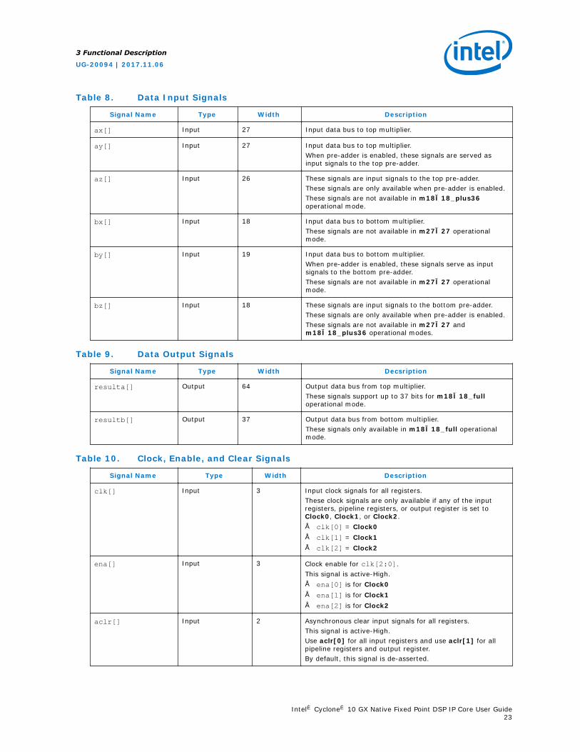
Table 8. Data Input Signals
Signal Name Type Width Description
ax[] Input 27 Input data bus to top multiplier.
ay[] Input 27 Input data bus to top multiplier.When pre-adder is enabled, these signals are served asinput signals to the top pre-adder.
az[] Input 26 These signals are input signals to the top pre-adder.These signals are only available when pre-adder is enabled.These signals are not available in m18×18_plus36operational mode.
bx[] Input 18 Input data bus to bottom multiplier.These signals are not available in m27×27 operationalmode.
by[] Input 19 Input data bus to bottom multiplier.When pre-adder is enabled, these signals serve as inputsignals to the bottom pre-adder.These signals are not available in m27×27 operationalmode.
bz[] Input 18 These signals are input signals to the bottom pre-adder.These signals are only available when pre-adder is enabled.These signals are not available in m27×27 andm18×18_plus36 operational modes.
Table 9. Data Output Signals
Signal Name Type Width Decsription
resulta[] Output 64 Output data bus from top multiplier.These signals support up to 37 bits for m18×18_fulloperational mode.
resultb[] Output 37 Output data bus from bottom multiplier.These signals only available in m18×18_full operationalmode.
Table 10. Clock, Enable, and Clear Signals
Signal Name Type Width Description
clk[] Input 3 Input clock signals for all registers.These clock signals are only available if any of the inputregisters, pipeline registers, or output register is set toClock0, Clock1, or Clock2.• clk[0] = Clock0• clk[1] = Clock1• clk[2] = Clock2
ena[] Input 3 Clock enable for clk[2:0].This signal is active-High.• ena[0] is for Clock0• ena[1] is for Clock1• ena[2] is for Clock2
aclr[] Input 2 Asynchronous clear input signals for all registers.This signal is active-High.Use aclr[0] for all input registers and use aclr[1] for allpipeline registers and output register.By default, this signal is de-asserted.
3 Functional Description
UG-20094 | 2017.11.06
Intel® Cyclone® 10 GX Native Fixed Point DSP IP Core User Guide23
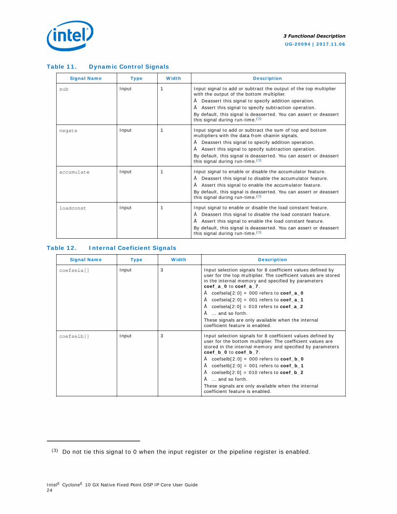
Table 11. Dynamic Control Signals
Signal Name Type Width Description
sub Input 1 Input signal to add or subtract the output of the top multiplierwith the output of the bottom multiplier.• Deassert this signal to specify addition operation.• Assert this signal to specify subtraction operation.By default, this signal is deasserted. You can assert or deassertthis signal during run-time.(3)
negate Input 1 Input signal to add or subtract the sum of top and bottommultipliers with the data from chainin signals.• Deassert this signal to specify addition operation.• Assert this signal to specify subtraction operation.By default, this signal is deasserted. You can assert or deassertthis signal during run-time.(3)
accumulate Input 1 Input signal to enable or disable the accumulator feature.• Deassert this signal to disable the accumulator feature.• Assert this signal to enable the accumulator feature.By default, this signal is deasserted. You can assert or deassertthis signal during run-time.(3)
loadconst Input 1 Input signal to enable or disable the load constant feature.• Deassert this signal to disable the load constant feature.• Assert this signal to enable the load constant feature.By default, this signal is deasserted. You can assert or deassertthis signal during run-time.(3)
Table 12. Internal Coeficient Signals
Signal Name Type Width Description
coefsela[] Input 3 Input selection signals for 8 coefficient values defined byuser for the top multiplier. The coefficient values are storedin the internal memory and specified by parameterscoef_a_0 to coef_a_7.• coefsela[2:0] = 000 refers to coef_a_0• coefsela[2:0] = 001 refers to coef_a_1• coelsela[2:0] = 010 refers to coef_a_2• ... and so forth.These signals are only available when the internalcoefficient feature is enabled.
coefselb[] Input 3 Input selection signals for 8 coefficient values defined byuser for the bottom multiplier. The coefficient values arestored in the internal memory and specified by parameterscoef_b_0 to coef_b_7.• coefselb[2:0] = 000 refers to coef_b_0• coefselb[2:0] = 001 refers to coef_b_1• coelselb[2:0] = 010 refers to coef_b_2• ... and so forth.These signals are only available when the internalcoefficient feature is enabled.
(3) Do not tie this signal to 0 when the input register or the pipeline register is enabled.
3 Functional Description
UG-20094 | 2017.11.06
Intel® Cyclone® 10 GX Native Fixed Point DSP IP Core User Guide24
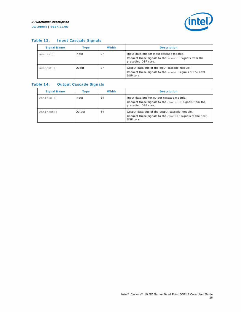
Table 13. Input Cascade Signals
Signal Name Type Width Description
scanin[] Input 27 Input data bus for input cascade module.Connect these signals to the scanout signals from thepreceding DSP core.
scanout[] Ouput 27 Output data bus of the input cascade module.Connect these signals to the scanin signals of the nextDSP core.
Table 14. Output Cascade Signals
Signal Name Type Width Description
chainin[] Input 64 Input data bus for output cascade module.Connect these signals to the chainout signals from thepreceding DSP core.
chainout[] Output 64 Output data bus of the output cascade module.Connect these signals to the chainin signals of the nextDSP core.
3 Functional Description
UG-20094 | 2017.11.06
Intel® Cyclone® 10 GX Native Fixed Point DSP IP Core User Guide25
A Document Revision History for the Cyclone 10 GX NativeFixed Point DSP IP Core User Guide
Date Version Changes
November 2017 2017.11.06 Initial release.
UG-20094 | 2017.11.06
Intel Corporation. All rights reserved. Intel, the Intel logo, Altera, Arria, Cyclone, Enpirion, MAX, Nios, Quartusand Stratix words and logos are trademarks of Intel Corporation or its subsidiaries in the U.S. and/or othercountries. Intel warrants performance of its FPGA and semiconductor products to current specifications inaccordance with Intel's standard warranty, but reserves the right to make changes to any products and servicesat any time without notice. Intel assumes no responsibility or liability arising out of the application or use of anyinformation, product, or service described herein except as expressly agreed to in writing by Intel. Intelcustomers are advised to obtain the latest version of device specifications before relying on any publishedinformation and before placing orders for products or services.*Other names and brands may be claimed as the property of others.
ISO9001:2008Registered