Embed Size (px)
Citation preview
Document Number:322167-002
Intel® Core™ i7-800 and i5-700 Desktop Processor Series and LGA1156 SocketThermal/Mechanical Specifications and Design Guidelines
September 2009
2 Thermal/Mechanical Specifications and Design Guidelines
INFORMATION IN THIS DOCUMENT IS PROVIDED IN CONNECTION WITH INTEL® PRODUCTS. NO LICENSE, EXPRESS OR IMPLIED, BY ESTOPPEL OR OTHERWISE, TO ANY INTELLECTUAL PROPERTY RIGHTS IS GRANTED BY THIS DOCUMENT. EXCEPT AS PROVIDED IN INTEL'S TERMS AND CONDITIONS OF SALE FOR SUCH PRODUCTS, INTEL ASSUMES NO LIABILITY WHATSOEVER, AND INTEL DISCLAIMS ANY EXPRESS OR IMPLIED WARRANTY, RELATING TO SALE AND/OR USE OF INTEL PRODUCTS INCLUDING LIABILITY OR WARRANTIES RELATING TO FITNESS FOR A PARTICULAR PURPOSE, MERCHANTABILITY, OR INFRINGEMENT OF ANY PATENT, COPYRIGHT OR OTHER INTELLECTUAL PROPERTY RIGHT. Intel products are not intended for use in medical, life saving, or life sustaining applications.
Intel may make changes to specifications and product descriptions at any time, without notice.
Designers must not rely on the absence or characteristics of any features or instructions marked “reserved” or “undefined.” Intel reserves these for future definition and shall have no responsibility whatsoever for conflicts or incompatibilities arising from future changes to them.
The Intel Core™ i7-800 and i5-700 desktop processor series and Intel® 5 Series Chipset and LGA1156 socket may contain design defects or errors known as errata which may cause the product to deviate from published specifications. Current characterized errata are available on request.
Contact your local Intel sales office or your distributor to obtain the latest specifications and before placing your product order.
Intel, Core and the Intel logo are trademarks of Intel Corporation in the U.S and other countries.
* Other brands and names may be claimed as the property of others.
Copyright © 2009 Intel Corporation.
Thermal/Mechanical Specifications and Design Guidelines 3
Contents
1 Introduction ..............................................................................................................91.1 References .........................................................................................................91.2 Definition of Terms ............................................................................................ 10
2 Package Mechanical and Storage Specifications....................................................... 112.1 Package Mechanical Specifications ....................................................................... 11
2.1.1 Package Mechanical Drawing.................................................................... 122.1.2 Processor Component Keep-Out Zones...................................................... 122.1.3 Package Loading Specifications ................................................................ 132.1.4 Package Handling Guidelines.................................................................... 132.1.5 Package Insertion Specifications............................................................... 132.1.6 Processor Mass Specification.................................................................... 132.1.7 Processor Materials................................................................................. 142.1.8 Processor Markings................................................................................. 142.1.9 Processor Land Coordinates ..................................................................... 15
2.2 Processor Storage Specifications ......................................................................... 16
3 LGA1156 Socket ...................................................................................................... 173.1 Board Layout .................................................................................................... 193.2 Attachment to Motherboard ................................................................................ 203.3 Socket Components........................................................................................... 20
3.3.1 Socket Body Housing .............................................................................. 203.3.2 Solder Balls ........................................................................................... 213.3.3 Contacts ............................................................................................... 213.3.4 Pick and Place Cover............................................................................... 21
3.4 Package Installation / Removal ........................................................................... 223.4.1 Socket Standoffs and Package Seating Plane.............................................. 23
3.5 Durability ......................................................................................................... 233.6 Markings .......................................................................................................... 243.7 Component Insertion Forces ............................................................................... 243.8 Socket Size ...................................................................................................... 24
4 Independent Loading Mechanism (ILM)................................................................... 254.1 Design Concept................................................................................................. 25
4.1.1 ILM Cover Assembly Design Overview ....................................................... 254.1.2 ILM Back Plate Design Overview............................................................... 264.1.3 Shoulder Screw and Fasteners Design Overview ......................................... 27
4.2 Assembly of ILM to a Motherboard....................................................................... 284.3 ILM Interchangeability ....................................................................................... 294.4 Markings .......................................................................................................... 29
5 LGA1156 Socket and ILM Electrical, Mechanical, and Environmental Specifications . 315.1 Component Mass............................................................................................... 315.2 Package/Socket Stackup Height .......................................................................... 315.3 Socket Maximum Temperature............................................................................ 325.4 Loading Specifications........................................................................................ 325.5 Electrical Requirements...................................................................................... 335.6 Environmental Requirements .............................................................................. 34
6 Thermal Specifications ............................................................................................ 356.1 Thermal Specifications ....................................................................................... 35
6.1.1 Intel® Core™ i7-800 and i5-700 Desktop Processor Series Thermal Profile ..... 376.1.2 Processor Specification for Operation Where Digital
Thermal Sensor Exceeds TCONTROL ............................................................ 39

4 Thermal/Mechanical Specifications and Design Guidelines
6.1.3 Thermal Metrology..................................................................................406.2 Processor Thermal Features ................................................................................40
6.2.1 Processor Temperature............................................................................406.2.2 Adaptive Thermal Monitor ........................................................................416.2.3 THERMTRIP# Signal ................................................................................44
6.3 Platform Environment Control Interface (PECI) ......................................................446.3.1 Introduction...........................................................................................446.3.2 PECI Client Capabilities............................................................................456.3.3 Temperature Data ..................................................................................45
7 Sensor Based Thermal Specification Design Guidance ..............................................477.1 Sensor Based Specification Overview....................................................................477.2 Sensor Based Thermal Specification .....................................................................49
7.2.1 TTV Thermal Profile.................................................................................497.2.2 Specification When DTS value is Greater than TCONTROL ...............................50
7.3 Thermal Solution Design Process .........................................................................517.3.1 Boundary Condition Definition ..................................................................517.3.2 Thermal Design and Modelling ..................................................................527.3.3 Thermal Solution Validation......................................................................52
7.4 Fan Speed Control (FSC) design process ...............................................................547.4.1 Fan Speed Control Algorithm without TAMBIENT Data ....................................547.4.2 Fan Speed Control Algorithm with TAMBIENT Data.........................................55
7.5 System Validation..............................................................................................577.6 Thermal Solution Characterization........................................................................58
8 ATX Reference Thermal Solution ..............................................................................598.1 Heatsink Thermal Solution ..................................................................................598.2 Geometric Envelope for the Intel Reference ATX Thermal Mechanical Design..............608.3 Heatsink Mass and Center of Gravity ....................................................................608.4 Thermal Interface Material ..................................................................................60
9 Thermal Solution Quality and Reliability Requirements ............................................619.1 Reference Heatsink Thermal Verification ...............................................................619.2 Mechanical Environmental Testing........................................................................61
9.2.1 Recommended Test Sequence ..................................................................629.2.2 Post-Test Pass Criteria.............................................................................629.2.3 Recommended BIOS/Processor/Memory Test Procedures .............................62
9.3 Material and Recycling Requirements....................................................................63
10 Boxed Processor Specifications................................................................................6510.1 Introduction......................................................................................................6510.2 Mechanical Specifications....................................................................................66
10.2.1 Boxed Processor Cooling Solution Dimensions.............................................6610.2.2 Boxed Processor Fan Heatsink Weight .......................................................6810.2.3 Boxed Processor Retention Mechanism and Heatsink Attach Clip Assembly .....68
10.3 Electrical Requirements ......................................................................................6810.3.1 Fan Heatsink Power Supply ......................................................................68
10.4 Thermal Specifications........................................................................................6910.4.1 Boxed Processor Cooling Requirements......................................................6910.4.2 Variable Speed Fan .................................................................................71
A Component Suppliers ...............................................................................................73B Mechanical Drawings ...............................................................................................75C Socket Mechanical Drawings ....................................................................................89D Package Mechanical Drawings .................................................................................95E Heat Sink Back Plate Drawings ................................................................................99
Thermal/Mechanical Specifications and Design Guidelines 5
Figures2-1 Processor Package Assembly Sketch ........................................................................ 112-2 Package View ....................................................................................................... 122-3 Processor Top-Side Markings .................................................................................. 142-4 Processor Package Lands Coordinates ...................................................................... 153-1 LGA1156 Socket with Pick and Place Cover ............................................................... 173-2 LGA1156 Socket Contact Numbering (Top View of Socket) .......................................... 183-3 LGA1156 Socket Land Pattern (Top View of Board) .................................................... 193-4 Attachment to Motherboard .................................................................................... 203-5 Pick and Place Cover.............................................................................................. 223-6 Package Installation / Removal Features................................................................... 234-1 ILM Cover Assembly .............................................................................................. 264-2 Back Plate ............................................................................................................ 264-3 Shoulder Screw..................................................................................................... 274-4 ILM Assembly ....................................................................................................... 284-5 Pin 1 and ILM Lever............................................................................................... 295-1 Flow Chart of Knowledge-Based Reliability Evaluation Methodology .............................. 346-1 Thermal Test Vehicle Thermal Profile for Intel® Core™ i7-800 and i5-700 Desktop
Processor Series.................................................................................................... 376-2 TTV Case Temperature (TCASE) Measurement Location .............................................. 406-3 Frequency and Voltage Ordering.............................................................................. 426-4 Temperature Sensor Data Format............................................................................ 457-1 Comparison of Case Temperature versus Sensor Based Specification............................ 487-2 Intel® Core™ i7-800 and i5-700 Desktop Processor Series Thermal Profile .................... 497-3 Thermal solution Performance................................................................................. 507-4 Required YCA for Various TAMBIENT Conditions ........................................................... 527-5 Thermal Solution Performance versus Fan Speed....................................................... 537-6 Fan Response Without TAMBIENT Data ....................................................................... 557-7 Fan Response with TAMBIENT Aware FSC.................................................................... 568-1 ATX Heatsink Reference Design Assembly................................................................. 598-2 ATX KOZ 3-D Model Primary (Top) Side.................................................................... 6010-1 Boxed Processor Fan Heatsink................................................................................. 6510-2 Space Requirements for the Boxed Processor (side view)............................................ 6610-3 Space Requirements for the Boxed Processor (top view)............................................. 6710-4 Space Requirements for the Boxed Processor (overall view) ........................................ 6710-5 Boxed Processor Fan Heatsink Power Cable Connector Description ............................... 6810-6 Baseboard Power Header Placement Relative to Processor Socket ................................ 6910-7 Boxed Processor Fan Heatsink Airspace Keepout Requirements (top view) .................... 7010-8 Boxed Processor Fan Heatsink Airspace Keepout Requirements (side view) ................... 7010-9 Boxed Processor Fan Heatsink Set Points.................................................................. 71B-1 Socket / Heatsink / ILM Keepout Zone Primary Side (Top) .......................................... 76B-2 Socket / Heatsink / ILM Keepout Zone Secondary Side (Bottom) ................................. 77B-3 Socket / Processor / ILM Keepout Zone Primary Side (Top) ......................................... 78B-4 Socket / Processor / ILM Keepout Zone Secondary Side (Bottom) ................................ 79B-5 Reference Design Heatsink Assembly ....................................................................... 80B-6 Reference Fastener (Sheet 1 of 4) ........................................................................... 81B-7 Reference Fastener (Sheet 2 of 4) ........................................................................... 82B-8 Reference Fastener (Sheet 3 of 4) ........................................................................... 83B-9 Reference Fastener (Sheet 4 of 4) ........................................................................... 84B-10 Reference Clip (Sheet 1 of 2) .................................................................................. 85B-11 Reference Clip (Sheet 2 of 2) .................................................................................. 86B-12 Thermocouple Attach Drawing................................................................................. 87C-1 Socket Mechanical Drawing (Sheet 1 of 4) ................................................................ 90
6 Thermal/Mechanical Specifications and Design Guidelines
C-2 Socket Mechanical Drawing (Sheet 2 of 4).................................................................91C-3 Socket Mechanical Drawing (Sheet 3 of 4).................................................................92C-4 Socket Mechanical Drawing (Sheet 4 of 4).................................................................93D-1 Processor Package Drawing (Sheet 1 of 2) ................................................................96D-2 Processor Package Drawing (Sheet 2 of 2) ................................................................97E-1 Heat Sink Back Plate Keep In Zone ........................................................................100E-2 Heat Sink Back Plate ............................................................................................101
Thermal/Mechanical Specifications and Design Guidelines 7
Tables1-1 Reference Documents ..............................................................................................91-2 Terms and Descriptions.......................................................................................... 102-1 Processor Loading Specifications ............................................................................. 132-2 Package Handling Guidelines................................................................................... 132-3 Processor Materials................................................................................................ 142-4 Storage Conditions ................................................................................................ 165-1 Socket Component Mass ........................................................................................ 315-2 1156-land Package and LGA1156 Socket Stackup Height ............................................ 315-3 Socket & ILM Mechanical Specifications .................................................................... 325-4 Electrical Requirements for LGA1156 Socket ............................................................. 336-1 Processor Thermal Specifications ............................................................................. 366-2 Thermal Test Vehicle Thermal Profile for Intel® Core™ i7-800 and i5-700 Desktop
Processor Series.................................................................................................... 386-3 Thermal Solution Performance above TCONTROL for the Intel® Core™ i7-800 and
i5-700 Desktop Processor Series ............................................................................. 396-4 Supported PECI Command Functions and Codes ........................................................ 456-5 Error Codes and Descriptions .................................................................................. 467-1 Thermal Solution Performance above TCONTROL.......................................................... 588-1 Reference Thermal Solutions................................................................................... 599-1 Use Conditions (Board Level) .................................................................................. 6110-1 Fan Heatsink Power and Signal Specifications............................................................ 6910-2 Fan Heatsink Set Points.......................................................................................... 71A-1 Reference Heatsink Enabled Components ................................................................. 73A-2 LGA1156 Socket and ILM Components ..................................................................... 73A-3 Supplier Contact Information .................................................................................. 74B-1 Mechanical Drawing List ......................................................................................... 75C-1 Mechanical Drawing List ......................................................................................... 89D-1 Mechanical Drawing List ......................................................................................... 95E-1 Mechanical Drawing List ......................................................................................... 99E-2 Supplier Contact Information .................................................................................. 99
8 Thermal/Mechanical Specifications and Design Guidelines
Revision History
§
Revision Number Description Revision Date
-001 • Initial release September 2009
-002• Updated Tables A-2 and A-3.• Updated Chapters 3, 4, 8, and Appendix B
September 2009
Thermal/Mechanical Specifications and Design Guidelines 9
Introduction
1 Introduction
This document differs from previous Thermal and Mechanical Design Guidelines. In this document, mechanical and thermal specifications for the processor and the associated socket are now included. The usual design guidance has been retained.
The components described in this document include:
• The thermal and mechanical specifications for the
— Intel Core™ i7-800 and i5-700 desktop processor series
• The LGA1156 socket and the Independent Loading Mechanism (ILM) and back plate.
• The reference design thermal solution (heatsink) for the processors and associated retention hardware.
Note: When the information is applicable to all products, the this document will use “processor” or “processors” to simplify the document.
1.1 ReferencesMaterial and concepts available in the following documents may be beneficial when reading this document.
Table 1-1. Reference Documents
Document Location
Intel® Core™ i7-800 and i5-700 Desktop Processor Series Datasheet, Volume 1http://download.intel.com/design/processor/datashts/
322164.pdf
Intel® Core™ i7-800 and i5-700 Desktop Processor Series Datasheet, Volume 2http://download.intel.com/design/processor/datashts/
322165.pdf
Intel® Core™ i7-800 and i5-700 Desktop Processor Series Specification Updatehttp://download.intel.com/
design/processor/specupdt/322166.pdf
Intel® 5 Series Chipset and Intel® 3400 Chipset Datasheet www.intel.com/Assets/PDF/datasheet/322169.pdf
Intel® 5 Series Chipset and Intel® 3400 Chipset Specification Updatewww.intel.com/Assets/
PDF/specupdate/322170.pdf
Intel® 5 Series Chipset and Intel® 3400 Chipset – Thermal Mechanical Specifications and Design Guidelines
www.intel.com/Assets/PDF/designguide/
322171.pdf
4-Wire Pulse Width Modulation (PWM) Controlled Fans http://www.formfactors.org/
Introduction
10 Thermal/Mechanical Specifications and Design Guidelines
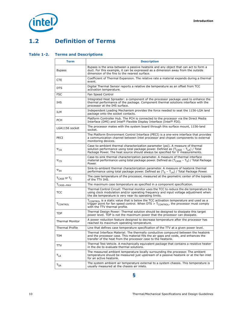
1.2 Definition of Terms
§
Table 1-2. Terms and Descriptions
Term Description
BypassBypass is the area between a passive heatsink and any object that can act to form a duct. For this example, it can be expressed as a dimension away from the outside dimension of the fins to the nearest surface.
CTE Coefficient of Thermal Expansion. The relative rate a material expands during a thermal event.
DTS Digital Thermal Sensor reports a relative die temperature as an offset from TCC activation temperature.
FSC Fan Speed Control
IHSIntegrated Heat Spreader: a component of the processor package used to enhance the thermal performance of the package. Component thermal solutions interface with the processor at the IHS surface.
ILM Independent Loading Mechanism provides the force needed to seat the 1156-LGA land package onto the socket contacts.
PCH Platform Controller Hub. The PCH is connected to the processor via the Direct Media Interface (DMI) and Intel® Flexible Display Interface (Intel® FDI).
LGA1156 socket The processor mates with the system board through this surface mount, 1156-land socket.
PECIThe Platform Environment Control Interface (PECI) is a one-wire interface that provides a communication channel between Intel processor and chipset components to external monitoring devices.
ΨCA
Case-to-ambient thermal characterization parameter (psi). A measure of thermal solution performance using total package power. Defined as (TCASE – TLA) / Total Package Power. The heat source should always be specified for Ψ measurements.
ΨCS
Case-to-sink thermal characterization parameter. A measure of thermal interface material performance using total package power. Defined as (TCASE – TS) / Total Package Power.
ΨSASink-to-ambient thermal characterization parameter. A measure of heatsink thermal performance using total package power. Defined as (TS – TLA) / Total Package Power.
TCASE or TCThe case temperature of the processor, measured at the geometric center of the topside of the TTV IHS.
TCASE_MAX The maximum case temperature as specified in a component specification.
TCCThermal Control Circuit: Thermal monitor uses the TCC to reduce the die temperature by using clock modulation and/or operating frequency and input voltage adjustment when the die temperature is very near its operating limits.
TCONTROL
TCONTROL is a static value that is below the TCC activation temperature and used as a trigger point for fan speed control. When DTS > TCONTROL, the processor must comply with the TTV thermal profile.
TDP Thermal Design Power: Thermal solution should be designed to dissipate this target power level. TDP is not the maximum power that the processor can dissipate.
Thermal Monitor A power reduction feature designed to decrease temperature after the processor has reached its maximum operating temperature.
Thermal Profile Line that defines case temperature specification of the TTV at a given power level.
TIMThermal Interface Material: The thermally conductive compound between the heatsink and the processor case. This material fills the air gaps and voids, and enhances the transfer of the heat from the processor case to the heatsink.
TTV Thermal Test Vehicle. A mechanically equivalent package that contains a resistive heater in the die to evaluate thermal solutions.
TLA
The measured ambient temperature locally surrounding the processor. The ambient temperature should be measured just upstream of a passive heatsink or at the fan inlet for an active heatsink.
TSAThe system ambient air temperature external to a system chassis. This temperature is usually measured at the chassis air inlets.
Thermal/Mechanical Specifications and Design Guidelines 11
Package Mechanical and Storage Specifications
2 Package Mechanical and Storage Specifications
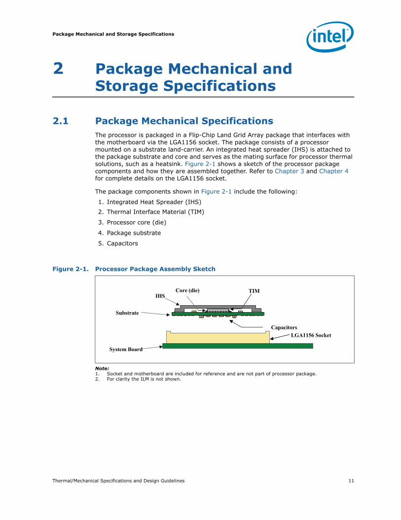
2.1 Package Mechanical SpecificationsThe processor is packaged in a Flip-Chip Land Grid Array package that interfaces with the motherboard via the LGA1156 socket. The package consists of a processor mounted on a substrate land-carrier. An integrated heat spreader (IHS) is attached to the package substrate and core and serves as the mating surface for processor thermal solutions, such as a heatsink. Figure 2-1 shows a sketch of the processor package components and how they are assembled together. Refer to Chapter 3 and Chapter 4 for complete details on the LGA1156 socket.
The package components shown in Figure 2-1 include the following:
1. Integrated Heat Spreader (IHS)
2. Thermal Interface Material (TIM)
3. Processor core (die)
4. Package substrate
5. Capacitors
Note:1. Socket and motherboard are included for reference and are not part of processor package.2. For clarity the ILM is not shown.
Figure 2-1. Processor Package Assembly Sketch
IHS
Substrate
System Board
Capacitors
Core (die) TIM
LGA1156 Socket
Package Mechanical and Storage Specifications
12 Thermal/Mechanical Specifications and Design Guidelines
2.1.1 Package Mechanical Drawing
Figure 2-2 shows the basic package layout and dimensions. The detailed package mechanical drawings are in Appendix D. The drawings include dimensions necessary to design a thermal solution for the processor. These dimensions include:
1. Package reference dimensions with tolerances (total height, length, width, and so forth.)
2. IHS parallelism and tilt
3. Land dimensions
4. Top-side and back-side component keep-out dimensions
5. Reference datums
6. All drawing dimensions are in mm
2.1.2 Processor Component Keep-Out Zones
The processor may contain components on the substrate that define component keep-out zone requirements. A thermal and mechanical solution design must not intrude into the required keep-out zones. Decoupling capacitors are typically mounted to either the topside or land-side of the package substrate. See Figure B-3 and Figure B-4 for keep-out zones. The location and quantity of package capacitors may change due to manufacturing efficiencies but will remain within the component keep-in. This keep-in zone includes solder paste and is a post reflow maximum height for the components.
Figure 2-2. Package View
37.5
3
7.5
Thermal/Mechanical Specifications and Design Guidelines 13
Package Mechanical and Storage Specifications
2.1.3 Package Loading Specifications
Table 2-1 provides dynamic and static load specifications for the processor package. These mechanical maximum load limits should not be exceeded during heatsink assembly, shipping conditions, or standard use condition. Also, any mechanical system or component testing should not exceed the maximum limits. The processor package substrate should not be used as a mechanical reference or load-bearing surface for thermal and mechanical solution.
.
Notes:1. These specifications apply to uniform compressive loading in a direction normal to the processor IHS.2. This is the maximum static force that can be applied by the heatsink and retention solution to maintain the
heatsink and processor interface.3. These specifications are based on limited testing for design characterization. Loading limits are for the
package only and do not include the limits of the processor socket.4. Dynamic loading is defined as an 50g shock load, 2X Dynamic Acceleration Factor with a 500g maximum
thermal solution.
2.1.4 Package Handling Guidelines
Table 2-2 includes a list of guidelines on package handling in terms of recommended maximum loading on the processor IHS relative to a fixed substrate. These package handling loads may be experienced during heatsink removal.
Notes:1. A shear load is defined as a load applied to the IHS in a direction parallel to the IHS top surface.2. A tensile load is defined as a pulling load applied to the IHS in a direction normal to the IHS surface.3. A torque load is defined as a twisting load applied to the IHS in an axis of rotation normal to the IHS top
surface.4. These guidelines are based on limited testing for design characterization.
2.1.5 Package Insertion Specifications
The processor can be inserted into and removed from an LGA1156 socket 15 times. The socket should meet the LGA1156 socket requirements detailed in Chapter 5.
2.1.6 Processor Mass Specification
The typical mass of the processor is 21.5g (0.76 oz). This mass [weight] includes all the components that are included in the package.
Table 2-1. Processor Loading Specifications
Parameter Minimum Maximum Notes
Static Compressive Load — 600 N [135 lbf] 1, 2, 3
Dynamic Compressive Load
— 712 N [160 lbf] 1, 3, 4
Table 2-2. Package Handling Guidelines
Parameter Maximum Recommended Notes
Shear 311 N [70 lbf] 1, 4
Tensile 111 N [25 lbf] 2, 4
Torque 3.95 N-m [35 lbf-in] 3, 4
Package Mechanical and Storage Specifications
14 Thermal/Mechanical Specifications and Design Guidelines
2.1.7 Processor Materials
Table 2-3 lists some of the package components and associated materials.
2.1.8 Processor Markings
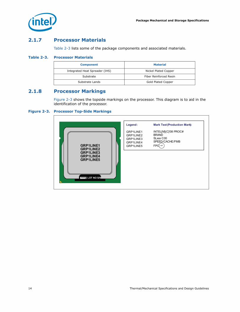
Figure 2-3 shows the topside markings on the processor. This diagram is to aid in the identification of the processor.
Table 2-3. Processor Materials
Component Material
Integrated Heat Spreader (IHS) Nickel Plated Copper
Substrate Fiber Reinforced Resin
Substrate Lands Gold Plated Copper
Figure 2-3. Processor Top-Side Markings
Legend:
GRP1LINE1GRP1LINE2GRP1LINE3GRP1LINE4GRP1LINE5
Mark Text (Production Mark):
INTEL{M}{C}'08 PROC#BRANDSLxxx C00SPEED/CACHE/FMBFPO
Legend:
GRP1LINE1GRP1LINE2GRP1LINE3GRP1LINE4GRP1LINE5
Mark Text (Engineering Mark):
INTEL{M}{C}'08 INTEL CONFIDENTIALQxxx ES C00 PRODUCT CODEFPO e4
e4GRP1LINE1GRP1LINE2GRP1LINE3GRP1LINE4GRP1LINE5
GRP1LINE1GRP1LINE2GRP1LINE3GRP1LINE4GRP1LINE5
LOT NO S/N
Thermal/Mechanical Specifications and Design Guidelines 15
Package Mechanical and Storage Specifications
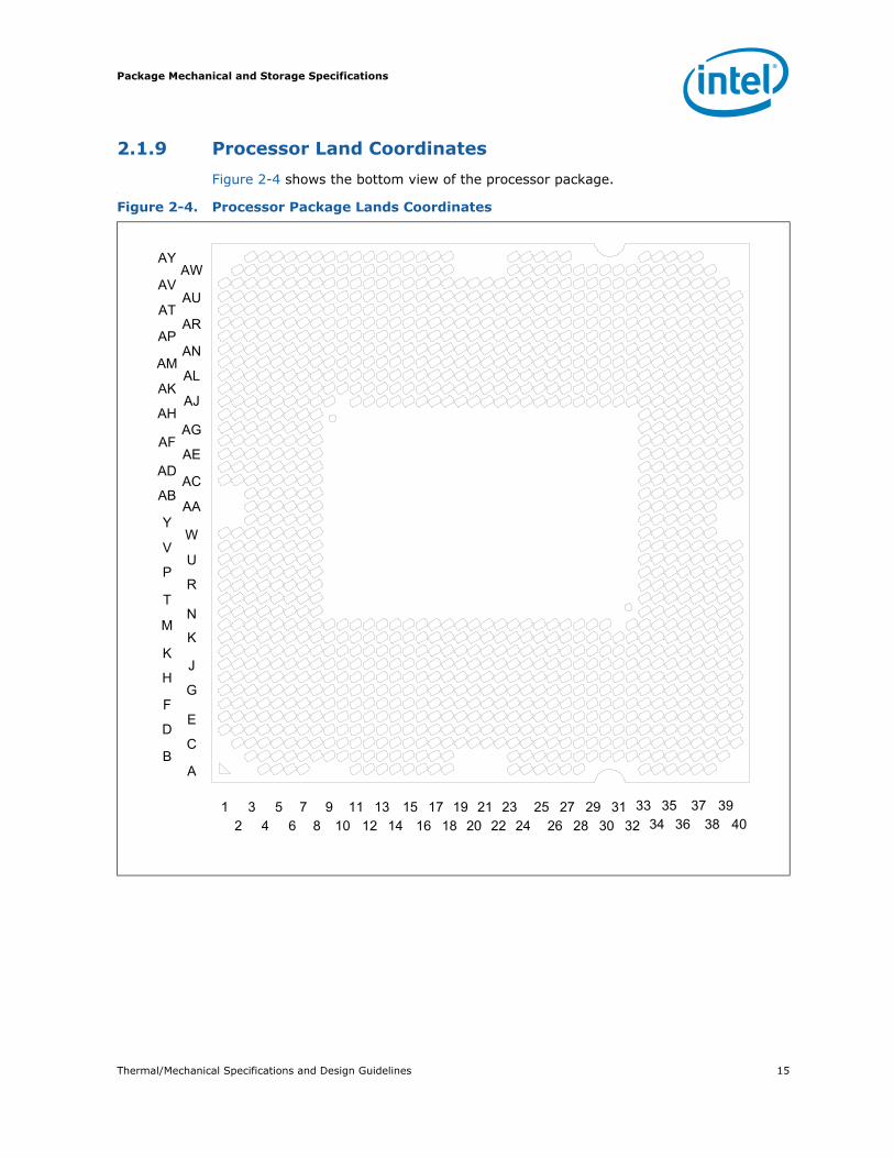
2.1.9 Processor Land Coordinates
Figure 2-4 shows the bottom view of the processor package..
Figure 2-4. Processor Package Lands Coordinates
AY
AV
AT
AP
AM
AK
AH
AF
AD
AB
Y
V
T
P
M
K
H
F
D
B
AW
AU
AR
AN
AL
AJ
AG
AE
AC
AA
W
U
N
R
K
J
G
E
C
A
1 3 5 7 9 11 13 15 17 19 21 23 25 27 29 31 33 35 37 392 4 6 8 10 12 14 16 18 20 22 24 26 28 30 32 34 36 38 40
Package Mechanical and Storage Specifications
16 Thermal/Mechanical Specifications and Design Guidelines
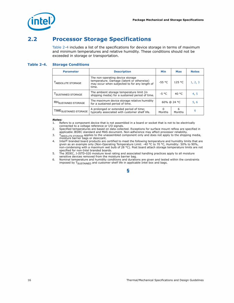
2.2 Processor Storage SpecificationsTable 2-4 includes a list of the specifications for device storage in terms of maximum and minimum temperatures and relative humidity. These conditions should not be exceeded in storage or transportation.
.
Notes:1. Refers to a component device that is not assembled in a board or socket that is not to be electrically
connected to a voltage reference or I/O signals.2. Specified temperatures are based on data collected. Exceptions for surface mount reflow are specified in
applicable JEDEC standard and MAS document. Non-adherence may affect processor reliability.3. TABSOLUTE STORAGE applies to the unassembled component only and does not apply to the shipping media,
moisture barrier bags or desiccant.4. Intel® branded board products are certified to meet the following temperature and humidity limits that are
given as an example only (Non-Operating Temperature Limit: -40 °C to 70 °C, Humidity: 50% to 90%, non-condensing with a maximum wet bulb of 28 °C). Post board attach storage temperature limits are not specified for non-Intel branded boards.
5. The JEDEC, J-JSTD-020 moisture level rating and associated handling practices apply to all moisture sensitive devices removed from the moisture barrier bag.
6. Nominal temperature and humidity conditions and durations are given and tested within the constraints imposed by TSUSTAINED and customer shelf life in applicable Intel box and bags.
§
Table 2-4. Storage Conditions
Parameter Description Min Max Notes
TABSOLUTE STORAGE
The non-operating device storage temperature. Damage (latent or otherwise) may occur when subjected to for any length of time.
-55 °C 125 °C 1, 2, 3
TSUSTAINED STORAGEThe ambient storage temperature limit (in shipping media) for a sustained period of time. -5 °C 40 °C 4, 5
RHSUSTAINED STORAGEThe maximum device storage relative humidity for a sustained period of time. 60% @ 24 °C 5, 6
TIMESUSTAINED STORAGEA prolonged or extended period of time; typically associated with customer shelf life.
0 Months
6 Months 6
Thermal/Mechanical Specifications and Design Guidelines 17
LGA1156 Socket
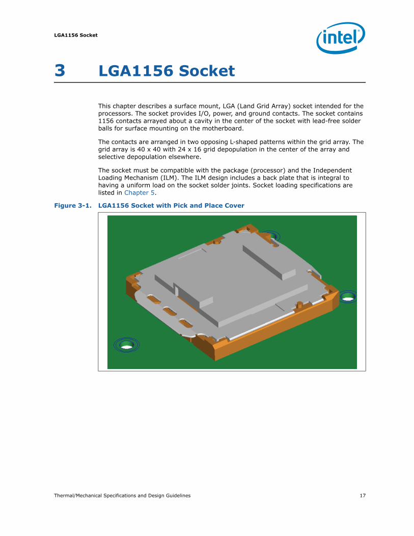
3 LGA1156 Socket
This chapter describes a surface mount, LGA (Land Grid Array) socket intended for the processors. The socket provides I/O, power, and ground contacts. The socket contains 1156 contacts arrayed about a cavity in the center of the socket with lead-free solder balls for surface mounting on the motherboard.
The contacts are arranged in two opposing L-shaped patterns within the grid array. The grid array is 40 x 40 with 24 x 16 grid depopulation in the center of the array and selective depopulation elsewhere.
The socket must be compatible with the package (processor) and the Independent Loading Mechanism (ILM). The ILM design includes a back plate that is integral to having a uniform load on the socket solder joints. Socket loading specifications are listed in Chapter 5.
Figure 3-1. LGA1156 Socket with Pick and Place Cover
LGA1156 Socket
18 Thermal/Mechanical Specifications and Design Guidelines
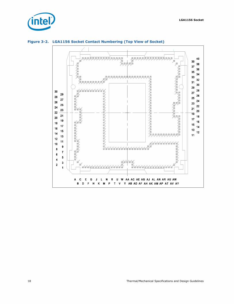
Figure 3-2. LGA1156 Socket Contact Numbering (Top View of Socket)
A C E G J L N R U W A A A C A E A G A J A L A N A R A U AWB D F H K M P T V Y A B A D A F A H A K A M A P A T A V A Y
1
3
7
5
9
11
15
13
17
19
23
21
25
27
29
2
8
4
6
10
16
12
14
18
24
20
22
26
28
30
15
11
13
17
23
19
21
25
31
27
29
33
39
35
37
32
14
12
16
18
22
20
24
26
30
28
34
38
36
40
A C E G J L N R U W A A A C A E A G A J A L A N A R A U AWB D F H K M P T V Y A B A D A F A H A K A M A P A T A V A Y
1
3
7
5
9
11
15
13
17
19
23
21
25
27
29
2
8
4
6
10
16
12
14
18
24
20
22
26
28
30
15
11
13
17
23
19
21
25
31
27
29
33
39
35
37
32
14
12
16
18
22
20
24
26
30
28
34
38
36
40
A C E G J L N R U W A A A C A E A G A J A L A N A R A U AWA C E G J L N R U W A A A C A E A G A J A L A N A R A U AWB D F H K M P T V Y A B A D A F A H A K A M A P A T A V A YB D F H K M P T V Y A B A D A F A H A K A M A P A T A V A Y
1
3
7
5
9
11
15
13
17
19
23
21
25
27
29
1
3
7
5
9
11
15
13
17
19
23
21
25
27
29
2
8
4
6
10
16
12
14
18
24
20
22
26
28
30
2
8
4
6
10
16
12
14
18
24
20
22
26
28
30
15
11
13
17
23
19
21
25
31
27
29
33
39
35
37
15
11
13
17
23
19
21
25
31
27
29
33
39
35
37
32
14
12
16
18
22
20
24
26
30
28
34
38
36
40
32
14
12
16
18
22
20
24
26
30
28
34
38
36
40
Thermal/Mechanical Specifications and Design Guidelines 19
LGA1156 Socket
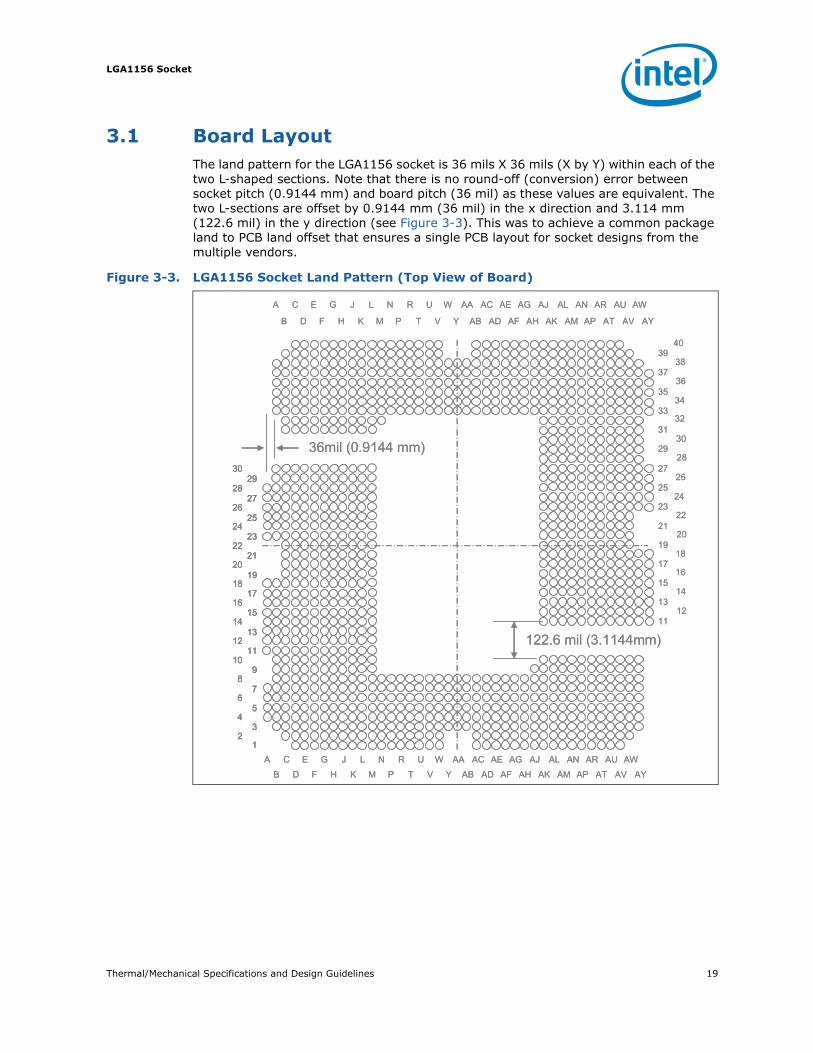
3.1 Board LayoutThe land pattern for the LGA1156 socket is 36 mils X 36 mils (X by Y) within each of the two L-shaped sections. Note that there is no round-off (conversion) error between socket pitch (0.9144 mm) and board pitch (36 mil) as these values are equivalent. The two L-sections are offset by 0.9144 mm (36 mil) in the x direction and 3.114 mm (122.6 mil) in the y direction (see Figure 3-3). This was to achieve a common package land to PCB land offset that ensures a single PCB layout for socket designs from the multiple vendors.
Figure 3-3. LGA1156 Socket Land Pattern (Top View of Board)
A C E G J L N R U W AA AC AE AG AJ AL AN AR AU AW
B D F H K M P T V Y AB AD AF AH AK AM AP AT AV AY
1
3
7
5
9
11
15
13
17
19
23
21
25
27
29
2
8
4
6
10
16
12
14
18
24
20
22
26
28
30
32
15
11
14
1213
1617
23
1918
22
2021
2425
31
2726
30
2829
33
39
3534
38
3637
40
B D F H K M P T V Y AB AD AF AH AK AM AP AT AV AY
A C E G J L N R U W AA AC AE AG AJ AL AN AR AU AW
122.6 mil (3.1144mm)
36mil (0.9144 mm)
A C E G J L N R U W AA AC AE AG AJ AL AN AR AU AW
B D F H K M P T V Y AB AD AF AH AK AM AP AT AV AY
1
3
7
5
9
11
15
13
17
19
23
21
25
27
29
1
3
7
5
9
11
15
13
17
19
23
21
25
27
29
2
8
4
6
10
16
12
14
18
24
20
22
26
28
30
2
8
4
6
10
16
12
14
18
24
20
22
26
28
30
32
15
11
14
1213
1617
23
1918
22
2021
2425
31
2726
30
2829
33
39
3534
38
3637
40
B D F H K M P T V Y AB AD AF AH AK AM AP AT AV AY
A C E G J L N R U W AA AC AE AG AJ AL AN AR AU AW
122.6 mil (3.1144mm)
36mil (0.9144 mm)
LGA1156 Socket
20 Thermal/Mechanical Specifications and Design Guidelines
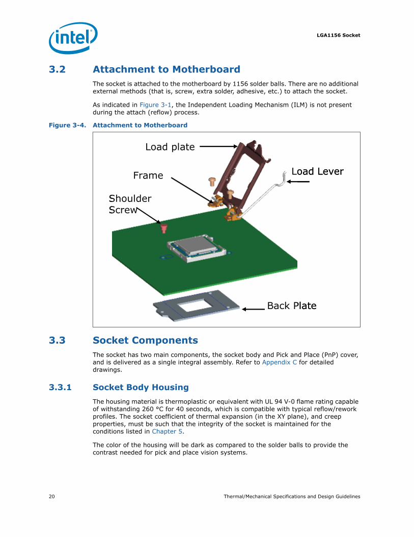
3.2 Attachment to MotherboardThe socket is attached to the motherboard by 1156 solder balls. There are no additional external methods (that is, screw, extra solder, adhesive, etc.) to attach the socket.
As indicated in Figure 3-1, the Independent Loading Mechanism (ILM) is not present during the attach (reflow) process.
3.3 Socket ComponentsThe socket has two main components, the socket body and Pick and Place (PnP) cover, and is delivered as a single integral assembly. Refer to Appendix C for detailed drawings.
3.3.1 Socket Body Housing
The housing material is thermoplastic or equivalent with UL 94 V-0 flame rating capable of withstanding 260 °C for 40 seconds, which is compatible with typical reflow/rework profiles. The socket coefficient of thermal expansion (in the XY plane), and creep properties, must be such that the integrity of the socket is maintained for the conditions listed in Chapter 5.
The color of the housing will be dark as compared to the solder balls to provide the contrast needed for pick and place vision systems.
Figure 3-4. Attachment to Motherboard
Load plate
Frame Load Lever
Back Plate
Shoulder Screw
Load plate
Frame Load Lever
Back Plate
Shoulder Screw
Thermal/Mechanical Specifications and Design Guidelines 21
LGA1156 Socket
3.3.2 Solder Balls
A total of 1156 solder balls corresponding to the contacts are on the bottom of the socket for surface mounting with the motherboard. The socket solder ball has the following characteristics:
• Lead free SAC (SnAgCu) 305 solder alloy with a silver (Ag) content between 3% and 4% and a melting temperature of approximately 217 °C. The alloy must be compatible with immersion silver (ImAg) and Organic Solderability Protectant (OSP) motherboard surface finishes and a SAC alloy solder paste.
The co-planarity (profile) and true position requirements are defined in Appendix C.
3.3.3 Contacts
Base material for the contacts is high strength copper alloy.
For the area on socket contacts where processor lands will mate, there is a 0.381 μm [15 μinches] minimum gold plating over 1.27 μm [50 μinches] minimum nickel underplate.
No contamination by solder in the contact area is allowed during solder reflow.
3.3.4 Pick and Place Cover
The cover provides a planar surface for vacuum pick up used to place components in the Surface Mount Technology (SMT) manufacturing line. The cover remains on the socket during reflow to help prevent contamination during reflow. The cover can withstand 260 °C for 40 seconds (typical reflow/rework profile) and the conditions listed in Chapter 5 without degrading.
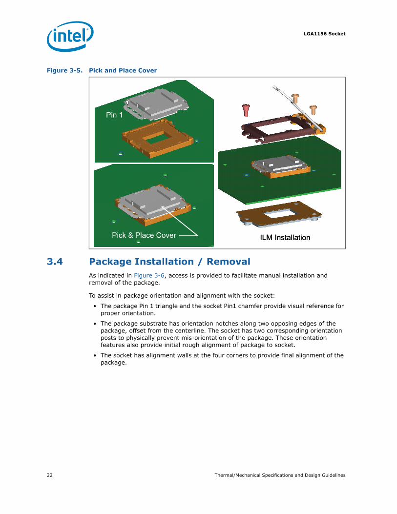
As indicated in Figure 3-5, the cover remains on the socket during ILM installation, and should remain on whenever possible to help prevent damage to the socket contacts.
Cover retention must be sufficient to support the socket weight during lifting, translation, and placement (board manufacturing), and during board and system shipping and handling. Covers can be removed without tools.
The socket vendors have a common interface on the socket body where the PnP cover attaches to the socket body. This should allow the PnP covers to be compatible between socket suppliers.
As indicated in Figure 3-5, a Pin1 indicator on the cover provides a visual reference for proper orientation with the socket.
LGA1156 Socket
22 Thermal/Mechanical Specifications and Design Guidelines
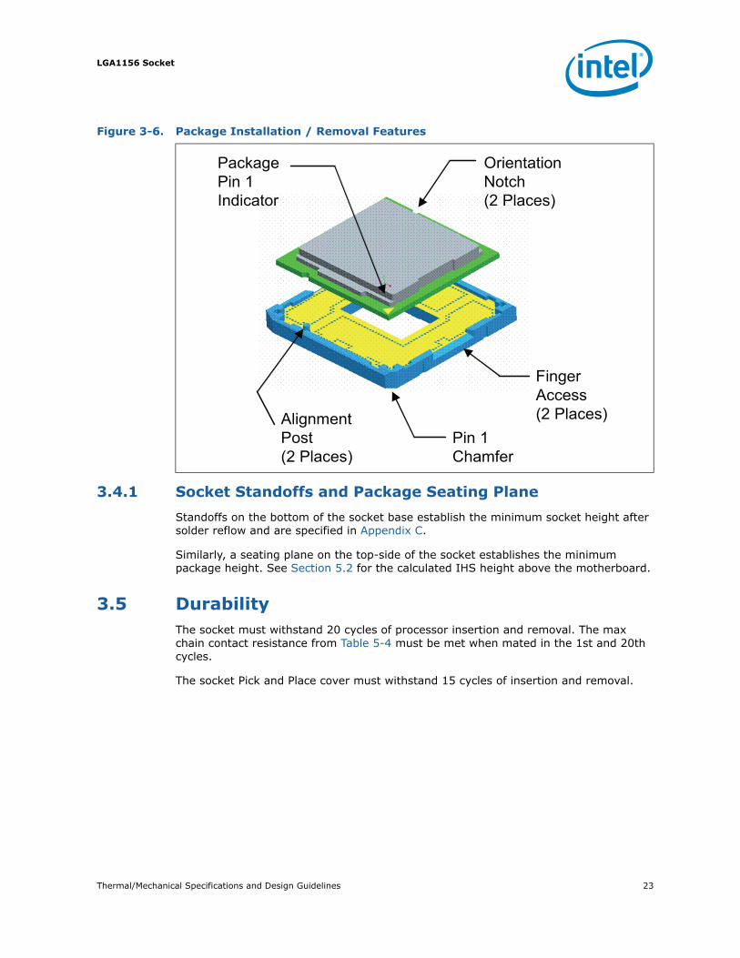
3.4 Package Installation / RemovalAs indicated in Figure 3-6, access is provided to facilitate manual installation and removal of the package.
To assist in package orientation and alignment with the socket:
• The package Pin 1 triangle and the socket Pin1 chamfer provide visual reference for proper orientation.
• The package substrate has orientation notches along two opposing edges of the package, offset from the centerline. The socket has two corresponding orientation posts to physically prevent mis-orientation of the package. These orientation features also provide initial rough alignment of package to socket.
• The socket has alignment walls at the four corners to provide final alignment of the package.
Figure 3-5. Pick and Place Cover
Pick & Place Cover
Pin 1
ILM InstallationPick & Place Cover
Pin 1
ILM Installation
Thermal/Mechanical Specifications and Design Guidelines 23
LGA1156 Socket
.
3.4.1 Socket Standoffs and Package Seating Plane
Standoffs on the bottom of the socket base establish the minimum socket height after solder reflow and are specified in Appendix C.
Similarly, a seating plane on the top-side of the socket establishes the minimum package height. See Section 5.2 for the calculated IHS height above the motherboard.
3.5 DurabilityThe socket must withstand 20 cycles of processor insertion and removal. The max chain contact resistance from Table 5-4 must be met when mated in the 1st and 20th cycles.
The socket Pick and Place cover must withstand 15 cycles of insertion and removal.
Figure 3-6. Package Installation / Removal Features
Pin 1 Chamfer
Package Pin 1 Indicator
Alignment Post(2 Places)
Finger Access(2 Places)
Orientation Notch(2 Places)
LGA1156 Socket
24 Thermal/Mechanical Specifications and Design Guidelines
3.6 MarkingsThere are three markings on the socket:
• LGA1156: Font type is Helvetica Bold - minimum 6 point (2.125 mm).
• Manufacturer's insignia (font size at supplier's discretion).
• Lot identification code (allows traceability of manufacturing date and location).
All markings must withstand 260°C for 40 seconds (typical reflow/rework profile) without degrading, and must be visible after the socket is mounted on the motherboard.
LGA1156 and the manufacturer's insignia are molded or laser marked on the side wall.
3.7 Component Insertion ForcesAny actuation must meet or exceed SEMI S8-95 Safety Guidelines for Ergonomics/Human Factors Engineering of Semiconductor Manufacturing Equipment, example Table R2-7 (Maximum Grip Forces). The socket must be designed so that it requires no force to insert the package into the socket.
3.8 Socket SizeSocket information needed for motherboard design is given in Appendix C.
This information should be used in conjunction with the reference motherboard keep-out drawings provided in Appendix B to ensure compatibility with the reference thermal mechanical components.
§
Thermal/Mechanical Specifications and Design Guidelines 25
Independent Loading Mechanism (ILM)
4 Independent Loading Mechanism (ILM)
The Independent Loading Mechanism (ILM) provides the force needed to seat the 1156-LGA land package onto the socket contacts. The ILM is physically separate from the socket body. The assembly of the ILM to the board is expected to occur after wave solder. The exact assembly location is dependent on manufacturing preference and test flow. See the Manufacturing Advantage Service collateral for this platform for additional guidance.
Note: The ILM has two critical functions: deliver the force to seat the processor onto the socket contacts and distribute the resulting compressive load evenly through the socket solder joints.
Note: The mechanical design of the ILM is integral to the overall functionality of the LGA1156 socket. Intel performs detailed studies on integration of processor package, socket and ILM as a system. These studies directly impact the design of the ILM. The Intel reference ILM will be “build to print” from Intel controlled drawings. Intel recommends using the Intel Reference ILM. Custom non-Intel ILM designs do not benefit from Intel's detailed studies and may not incorporate critical design parameters.
4.1 Design ConceptThe ILM consists of two assemblies that will be procured as a set from the enabled vendors. These two components are ILM cover assembly and back plate. To secure the two assemblies, two types of fasteners are required a pair (2) of standard 6-32 thread screws and a custom 6-32 thread shoulder screw. The reference design incorporates a T-20 Torx* head fastener. The Torx* head fastener was chosen to ensure end users do not inadvertently remove the ILM assembly and for consistency with the LGA1366 socket ILM. The Torx* head fastener is also less susceptible to driver slippage. Once assembled the ILM is not required to be removed to install / remove the motherboard from a chassis.
4.1.1 ILM Cover Assembly Design Overview
The ILM Cover assembly consists of three major pieces: load lever, load plate and the hinge frame assembly.
All of the pieces in the ILM cover assembly except the hinge frame and the screws used to attach the back plate are fabricated from stainless steel. The hinge frame is plated. The frame provides the hinge locations for the load lever and load plate. An insulator is pre-applied to the bottom surface of the hinge frame.
The cover assembly design ensures that once assembled to the back plate the only features touching the board are the shoulder screw and the insulated hinge frame assembly. The nominal gap of the load plate to the board is ~1 mm.
Independent Loading Mechanism (ILM)
26 Thermal/Mechanical Specifications and Design Guidelines
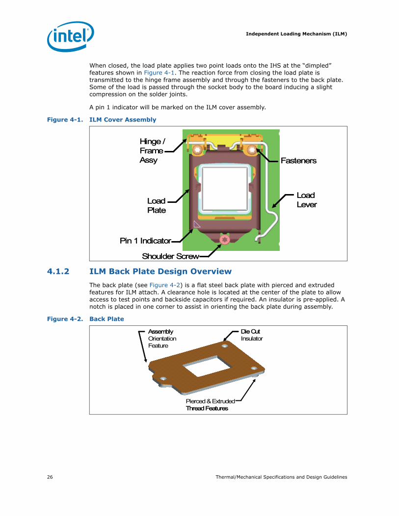
When closed, the load plate applies two point loads onto the IHS at the “dimpled” features shown in Figure 4-1. The reaction force from closing the load plate is transmitted to the hinge frame assembly and through the fasteners to the back plate. Some of the load is passed through the socket body to the board inducing a slight compression on the solder joints.
A pin 1 indicator will be marked on the ILM cover assembly.
4.1.2 ILM Back Plate Design Overview
The back plate (see Figure 4-2) is a flat steel back plate with pierced and extruded features for ILM attach. A clearance hole is located at the center of the plate to allow access to test points and backside capacitors if required. An insulator is pre-applied. A notch is placed in one corner to assist in orienting the back plate during assembly.
Figure 4-1. ILM Cover Assembly
Fasteners
Load LeverLoad
Plate
Hinge / Frame Assy
Shoulder Screw
Pin 1 Indicator
Fasteners
Load LeverLoad
Plate
Hinge / Frame Assy
Shoulder Screw
Pin 1 Indicator
Figure 4-2. Back Plate
Die Cut Insulator
Pierced & Extruded Thread Features
Assembly Orientation Feature
Die Cut Insulator
Pierced & Extruded Thread Features
Assembly Orientation Feature
Thermal/Mechanical Specifications and Design Guidelines 27
Independent Loading Mechanism (ILM)
4.1.3 Shoulder Screw and Fasteners Design Overview
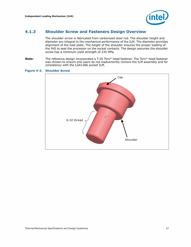
The shoulder screw is fabricated from carbonized steel rod. The shoulder height and diameter are integral to the mechanical performance of the ILM. The diameter provides alignment of the load plate. The height of the shoulder ensures the proper loading of the IHS to seat the processor on the socket contacts. The design assumes the shoulder screw has a minimum yield strength of 235 MPa.
Note: The reference design incorporates a T-20 Torx* head fastener. The Torx* head fastener was chosen to ensure end users do not inadvertently remove the ILM assembly and for consistency with the LGA1366 socket ILM.
Figure 4-3. Shoulder Screw
Shoulder
6-32 thread
Cap
Independent Loading Mechanism (ILM)
28 Thermal/Mechanical Specifications and Design Guidelines
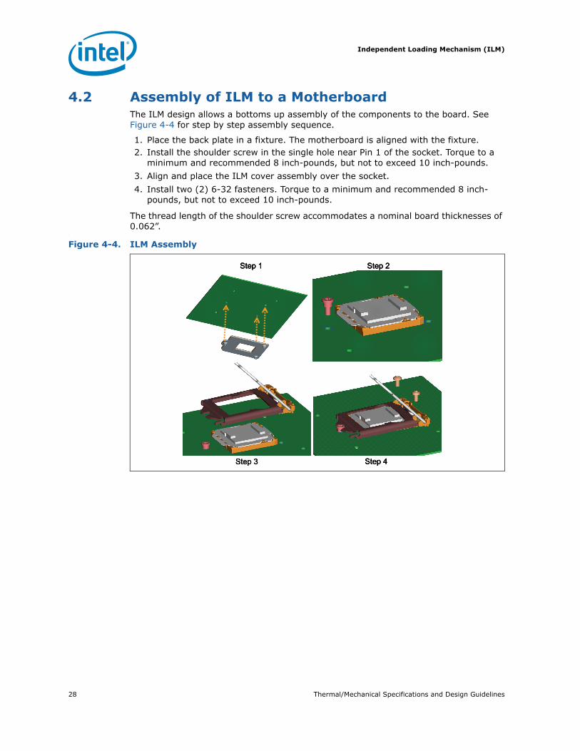
4.2 Assembly of ILM to a MotherboardThe ILM design allows a bottoms up assembly of the components to the board. See Figure 4-4 for step by step assembly sequence.
1. Place the back plate in a fixture. The motherboard is aligned with the fixture. 2. Install the shoulder screw in the single hole near Pin 1 of the socket. Torque to a
minimum and recommended 8 inch-pounds, but not to exceed 10 inch-pounds.
3. Align and place the ILM cover assembly over the socket.
4. Install two (2) 6-32 fasteners. Torque to a minimum and recommended 8 inch-pounds, but not to exceed 10 inch-pounds.
The thread length of the shoulder screw accommodates a nominal board thicknesses of 0.062”.
.
Figure 4-4. ILM Assembly
Step 1 Step 2
Step 3 Step 4
Step 1 Step 2
Step 3 Step 4
Step 1 Step 2
Step 3 Step 4
Thermal/Mechanical Specifications and Design Guidelines 29
Independent Loading Mechanism (ILM)
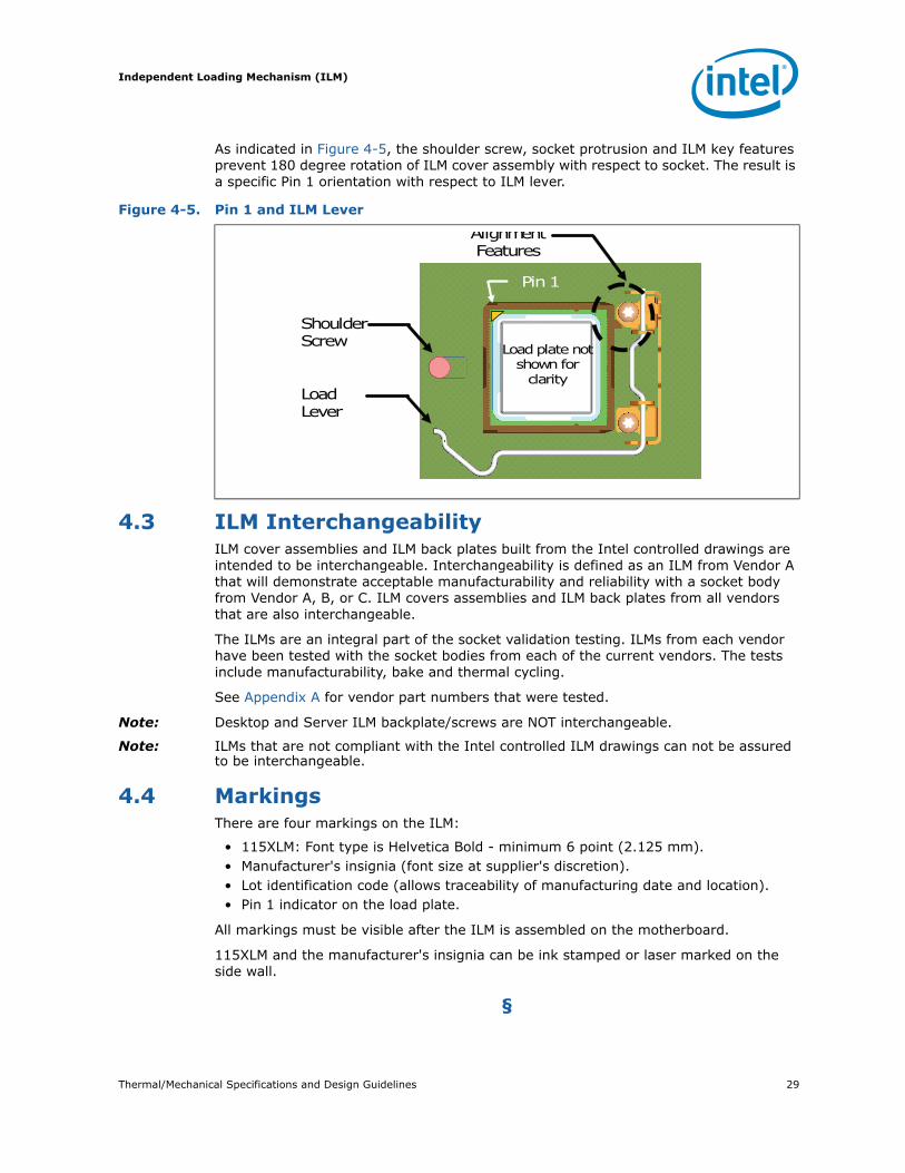
As indicated in Figure 4-5, the shoulder screw, socket protrusion and ILM key features prevent 180 degree rotation of ILM cover assembly with respect to socket. The result is a specific Pin 1 orientation with respect to ILM lever.
4.3 ILM InterchangeabilityILM cover assemblies and ILM back plates built from the Intel controlled drawings are intended to be interchangeable. Interchangeability is defined as an ILM from Vendor A that will demonstrate acceptable manufacturability and reliability with a socket body from Vendor A, B, or C. ILM covers assemblies and ILM back plates from all vendors that are also interchangeable.
The ILMs are an integral part of the socket validation testing. ILMs from each vendor have been tested with the socket bodies from each of the current vendors. The tests include manufacturability, bake and thermal cycling.
See Appendix A for vendor part numbers that were tested.
Note: Desktop and Server ILM backplate/screws are NOT interchangeable.
Note: ILMs that are not compliant with the Intel controlled ILM drawings can not be assured to be interchangeable.
4.4 MarkingsThere are four markings on the ILM:
• 115XLM: Font type is Helvetica Bold - minimum 6 point (2.125 mm).• Manufacturer's insignia (font size at supplier's discretion).• Lot identification code (allows traceability of manufacturing date and location).• Pin 1 indicator on the load plate.
All markings must be visible after the ILM is assembled on the motherboard.
115XLM and the manufacturer's insignia can be ink stamped or laser marked on the side wall.
§
Figure 4-5. Pin 1 and ILM Lever
Alignment Features
Load plate not shown for
clarity
Pin 1
ShoulderScrew
Load Lever

Independent Loading Mechanism (ILM)
30 Thermal/Mechanical Specifications and Design Guidelines
Thermal/Mechanical Specifications and Design Guidelines 31
LGA1156 Socket and ILM Electrical, Mechanical, and Environmental Specifications
5 LGA1156 Socket and ILM Electrical, Mechanical, and Environmental Specifications
This chapter describes the electrical, mechanical, and environmental specifications for the LGA1156 socket and the Independent Loading Mechanism.
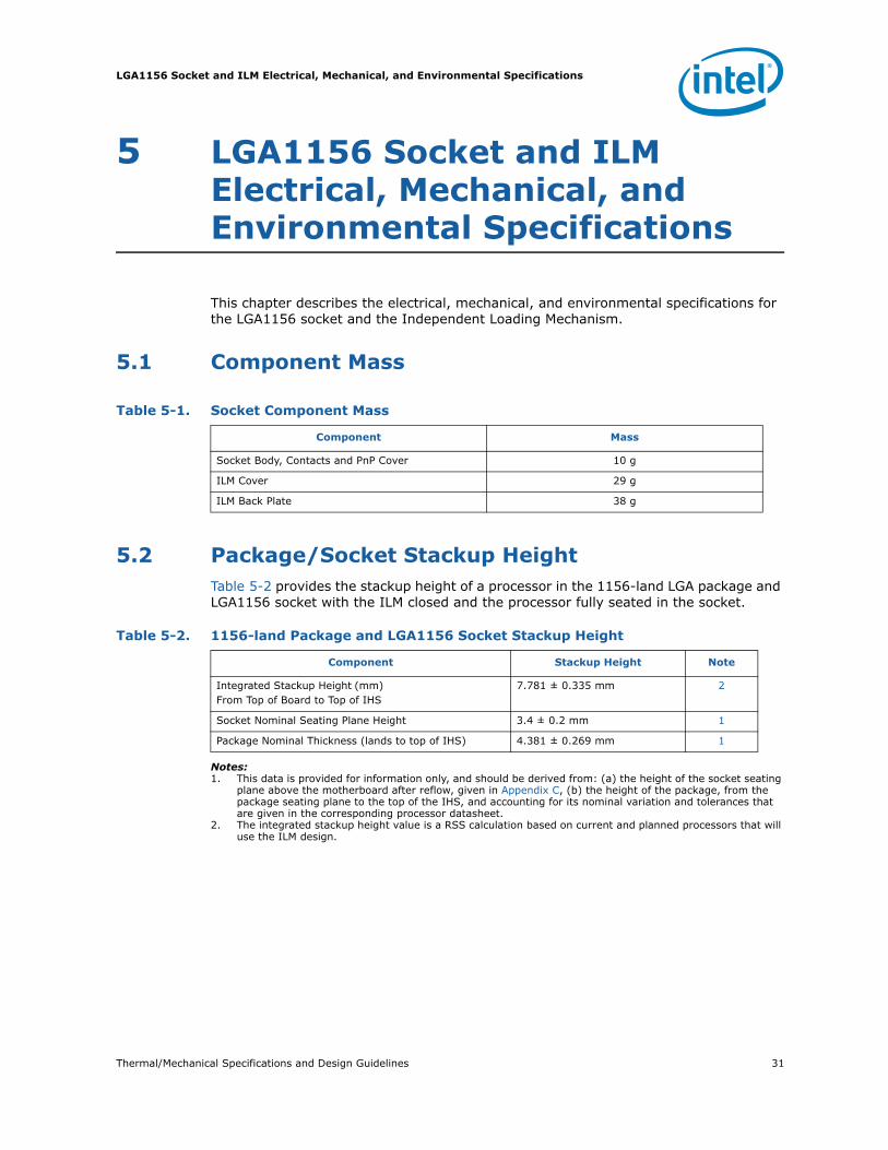
5.1 Component Mass
5.2 Package/Socket Stackup HeightTable 5-2 provides the stackup height of a processor in the 1156-land LGA package and LGA1156 socket with the ILM closed and the processor fully seated in the socket.
Notes:1. This data is provided for information only, and should be derived from: (a) the height of the socket seating
plane above the motherboard after reflow, given in Appendix C, (b) the height of the package, from the package seating plane to the top of the IHS, and accounting for its nominal variation and tolerances that are given in the corresponding processor datasheet.
2. The integrated stackup height value is a RSS calculation based on current and planned processors that will use the ILM design.
Table 5-1. Socket Component Mass
Component Mass
Socket Body, Contacts and PnP Cover 10 g
ILM Cover 29 g
ILM Back Plate 38 g
Table 5-2. 1156-land Package and LGA1156 Socket Stackup Height
Component Stackup Height Note
Integrated Stackup Height (mm)From Top of Board to Top of IHS
7.781 ± 0.335 mm 2
Socket Nominal Seating Plane Height 3.4 ± 0.2 mm 1
Package Nominal Thickness (lands to top of IHS) 4.381 ± 0.269 mm 1
LGA1156 Socket and ILM Electrical, Mechanical, and Environmental Specifications
32 Thermal/Mechanical Specifications and Design Guidelines
5.3 Socket Maximum TemperatureThe power dissipated within the socket is a function of the current at the pin level and the effective pin resistance. The key temperature limit for the LGA1156 socket is:
• Socket contact interface with package < 100 °C.
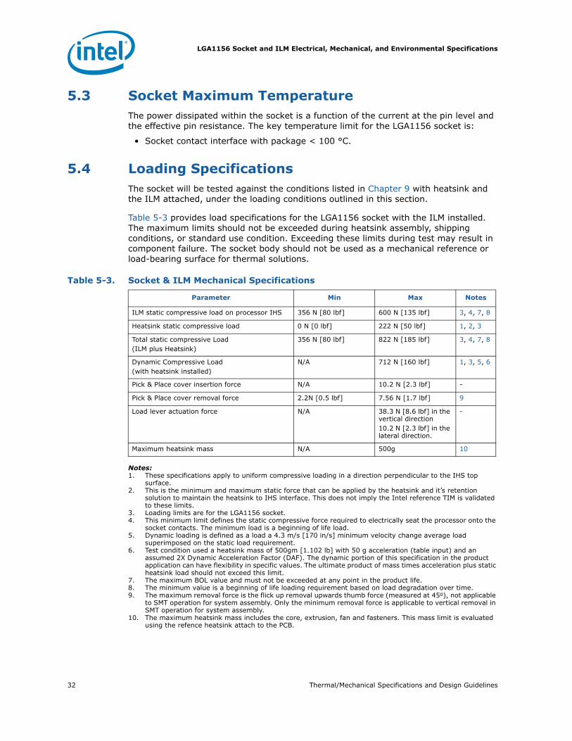
5.4 Loading SpecificationsThe socket will be tested against the conditions listed in Chapter 9 with heatsink and the ILM attached, under the loading conditions outlined in this section.
Table 5-3 provides load specifications for the LGA1156 socket with the ILM installed. The maximum limits should not be exceeded during heatsink assembly, shipping conditions, or standard use condition. Exceeding these limits during test may result in component failure. The socket body should not be used as a mechanical reference or load-bearing surface for thermal solutions.
Notes:1. These specifications apply to uniform compressive loading in a direction perpendicular to the IHS top
surface.2. This is the minimum and maximum static force that can be applied by the heatsink and it’s retention
solution to maintain the heatsink to IHS interface. This does not imply the Intel reference TIM is validated to these limits.
3. Loading limits are for the LGA1156 socket.4. This minimum limit defines the static compressive force required to electrically seat the processor onto the
socket contacts. The minimum load is a beginning of life load.5. Dynamic loading is defined as a load a 4.3 m/s [170 in/s] minimum velocity change average load
superimposed on the static load requirement.6. Test condition used a heatsink mass of 500gm [1.102 lb] with 50 g acceleration (table input) and an
assumed 2X Dynamic Acceleration Factor (DAF). The dynamic portion of this specification in the product application can have flexibility in specific values. The ultimate product of mass times acceleration plus static heatsink load should not exceed this limit.
7. The maximum BOL value and must not be exceeded at any point in the product life. 8. The minimum value is a beginning of life loading requirement based on load degradation over time.9. The maximum removal force is the flick up removal upwards thumb force (measured at 45o), not applicable
to SMT operation for system assembly. Only the minimum removal force is applicable to vertical removal in SMT operation for system assembly.
10. The maximum heatsink mass includes the core, extrusion, fan and fasteners. This mass limit is evaluated using the refence heatsink attach to the PCB.
Table 5-3. Socket & ILM Mechanical Specifications
Parameter Min Max Notes
ILM static compressive load on processor IHS 356 N [80 lbf] 600 N [135 lbf] 3, 4, 7, 8
Heatsink static compressive load 0 N [0 lbf] 222 N [50 lbf] 1, 2, 3
Total static compressive Load (ILM plus Heatsink)
356 N [80 lbf] 822 N [185 lbf] 3, 4, 7, 8
Dynamic Compressive Load (with heatsink installed)
N/A 712 N [160 lbf] 1, 3, 5, 6
Pick & Place cover insertion force N/A 10.2 N [2.3 lbf] -
Pick & Place cover removal force 2.2N [0.5 lbf] 7.56 N [1.7 lbf] 9
Load lever actuation force N/A 38.3 N [8.6 lbf] in the vertical direction 10.2 N [2.3 lbf] in the lateral direction.
-
Maximum heatsink mass N/A 500g 10
Thermal/Mechanical Specifications and Design Guidelines 33
LGA1156 Socket and ILM Electrical, Mechanical, and Environmental Specifications
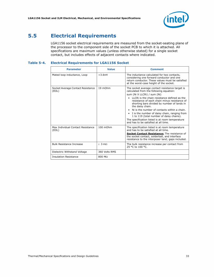
5.5 Electrical RequirementsLGA1156 socket electrical requirements are measured from the socket-seating plane of the processor to the component side of the socket PCB to which it is attached. All specifications are maximum values (unless otherwise stated) for a single socket contact, but includes effects of adjacent contacts where indicated.
Table 5-4. Electrical Requirements for LGA1156 Socket
Parameter Value Comment
Mated loop inductance, Loop <3.6nH The inductance calculated for two contacts, considering one forward conductor and one return conductor. These values must be satisfied at the worst-case height of the socket.
Socket Average Contact Resistance (EOL)
19 mOhm The socket average contact resistance target is calculated from the following equation:sum (Ni X LLCRi) / sum (Ni)• LLCRi is the chain resistance defined as the
resistance of each chain minus resistance of shorting bars divided by number of lands in the daisy chain.
• Ni is the number of contacts within a chain.• I is the number of daisy chain, ranging from
1 to 119 (total number of daisy chains).The specification listed is at room temperature and has to be satisfied at all time.
Max Individual Contact Resistance (EOL)
100 mOhm The specification listed is at room temperature and has to be satisfied at all time.Socket Contact Resistance: The resistance of the socket contact, solderball, and interface resistance to the interposer land; gaps included.
Bulk Resistance Increase ≤ 3 mΩ The bulk resistance increase per contact from 25 °C to 100 °C.
Dielectric Withstand Voltage 360 Volts RMS
Insulation Resistance 800 MΩ
LGA1156 Socket and ILM Electrical, Mechanical, and Environmental Specifications
34 Thermal/Mechanical Specifications and Design Guidelines
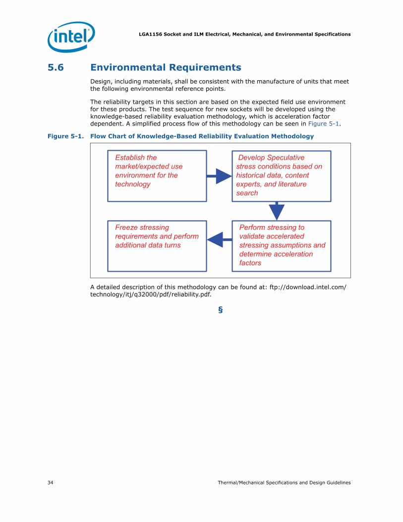
5.6 Environmental RequirementsDesign, including materials, shall be consistent with the manufacture of units that meet the following environmental reference points.
The reliability targets in this section are based on the expected field use environment for these products. The test sequence for new sockets will be developed using the knowledge-based reliability evaluation methodology, which is acceleration factor dependent. A simplified process flow of this methodology can be seen in Figure 5-1.
A detailed description of this methodology can be found at: ftp://download.intel.com/technology/itj/q32000/pdf/reliability.pdf.
§
Figure 5-1. Flow Chart of Knowledge-Based Reliability Evaluation Methodology
Establish the market/expected use environment for the technology
Develop Speculative stress conditions based on historical data, content experts, and literature search
Perform stressing to validate accelerated stressing assumptions and determine acceleration factors
Freeze stressing requirements and perform additional data turns
Thermal/Mechanical Specifications and Design Guidelines 35
Thermal Specifications
6 Thermal Specifications
The processor requires a thermal solution to maintain temperatures within its operating limits. Any attempt to operate the processor outside these operating limits may result in permanent damage to the processor and potentially other components within the system. Maintaining the proper thermal environment is key to reliable, long-term system operation.
A complete solution includes both component and system level thermal management features. Component level thermal solutions can include active or passive heatsinks attached to the processor integrated heat spreader (IHS).
This chapter provides data necessary for developing a complete thermal solution. For more information on ATX reference thermal solution design, refer to Chapter 8.
6.1 Thermal SpecificationsTo allow the optimal operation and long-term reliability of Intel processor-based systems, the processor must remain within the minimum and maximum case temperature (TCASE) specifications as defined by the applicable thermal profile. Thermal solutions not designed to provide this level of thermal capability may affect the long-term reliability of the processor and system. For more details on thermal solution design, refer to the Chapter 8.
The processors implement a methodology for managing processor temperatures which is intended to support acoustic noise reduction through fan speed control and to assure processor reliability. Selection of the appropriate fan speed is based on the relative temperature data reported by the processor’s Digital Temperature Sensor (DTS). The DTS can be read using the Platform Environment Control Interface (PECI) as described in Section 6.3. Alternatively, when PECI is monitored by the PCH, the processor temperature can be read from the PCH using the SMBus protocol defined in Embedded Controller Support Provided by Platform Controller Hub (PCH). The temperature reported over PECI is always a negative value and represents a delta below the onset of thermal control circuit (TCC) activation, as indicated by PROCHOT# (see Section 6.2, Processor Thermal Features). Systems that implement fan speed control must be designed to use this data. Systems that do not alter the fan speed only need to ensure the case temperature meets the thermal profile specifications.
A single integer change in the PECI value corresponds to approximately 1 °C change in processor temperature. Although each processors DTS is factory calibrated, the accuracy of the DTS will vary from part to part and may also vary slightly with temperature and voltage. In general, each integer change in PECI should equal a temperature change between 0.9 °C and 1.1 °C.
Analysis indicates that real applications are unlikely to cause the processor to consume maximum power dissipation for sustained time periods. Intel recommends that complete thermal solution designs target the Thermal Design Power (TDP), instead of the maximum processor power consumption. The Adaptive Thermal Monitor feature is intended to help protect the processor in the event that an application exceeds the TDP recommendation for a sustained time period. For more details on this feature, refer to
Thermal Specifications
36 Thermal/Mechanical Specifications and Design Guidelines
Section 6.2. To ensure maximum flexibility for future processors, systems should be designed to the Thermal Solution Capability guidelines, even if a processor with lower power dissipation is currently planned.
Notes:1. The package C-state power is the worst case power in the system configured as follows:
- Memory configured for DDR3 1333 and populated with 2 DIMM per channel.- DMI and PCIe links are at L1.
2. Specification at DTS = -50 and minimum voltage loadline.3. Specification at DTS = -50 and minimum voltage loadline.4. Specification at DTS = -64 and minimum voltage loadline.5. These DTS values (in Notes 2-4) are based on the TCC Activation MSR having a value of 100, see
Section 6.2.1.6. These values are specified at VCC_MAX and VNOM for all other voltage rails for all processor frequencies.
Systems must be designed to ensure the processor is not to be subjected to any static VCC and ICC combination wherein VCCP exceeds VCCP_MAX at specified ICCP. Refer to the loadline specifications in the datasheet.
7. Thermal Design Power (TDP) should be used for processor thermal solution design targets. TDP is not the maximum power that the processor can dissipate. TDP is measured at DTS = -1.TDP is achieved with the Memory configured for DDR3 1333 and 2 DIMMs per channel.
8. The 2009B (09B) guidelines provide a design target for meeting all planned processor frequency requirements. The 2009B (09B) is equivalent to the thermal requirements for the Intel® Core™ 2 Quad Q9000 processor series. The 2009A (09A) is equivalent to the thermal requirements for the Intel® Core™ 2 Duo E8000 processor series. Reuse of those thermal solutions is recommended with the updated mechanical attach to straddle the LGA1156 socket.
9. Not 100% tested. Specified by design characterization.
Table 6-1. Processor Thermal Specifications
Product Guidelines8
Max Power
Package C1E
(W)1,2,5,9
Max Power
Package C3
(W)1,3,5,9
Max Power
Package C6
(W)1,4,5,9
TTV Thermal Design Power(W)6,7
Min TCASE(°C)
Maximum TTV TCASE
(°C)
Intel Core™ i7-800 and i5-700 desktop processor series (95 W)
2009B(09B)
28 22 5.5 95 5 Figure 6-1 & Table 6-2
Thermal/Mechanical Specifications and Design Guidelines 37
Thermal Specifications
6.1.1 Intel® Core™ i7-800 and i5-700 Desktop Processor Series Thermal Profile
Notes:1. Please refer to Table 6-2 for discrete points that constitute the thermal profile.2. Refer to Chapter 8 and Chapter 9 for system and environmental implementation details.
Figure 6-1. Thermal Test Vehicle Thermal Profile for Intel® Core™ i7-800 and i5-700 Desktop Processor Series
TTV Thermal Profile
Y = Power x 0.29 + 45.1
40.0
45.0
50.0
55.0
60.0
65.0
70.0
75.0
0 20 40 60 80 100
TTV Power (W)
TTV
Cas
e Te
mpe
ratu
re (°
C)
Thermal Specifications
38 Thermal/Mechanical Specifications and Design Guidelines
Table 6-2. Thermal Test Vehicle Thermal Profile for Intel® Core™ i7-800 and i5-700 Desktop Processor Series
Power (W) TCASE_MAX (°C) Power (W) TCASE_MAX (°C)
0 45.1 50 59.6
2 45.7 52 60.2
4 46.3 54 60.8
6 46.8 56 61.3
8 47.4 58 61.9
10 48.0 60 62.5
12 48.6 62 63.1
14 49.2 64 63.7
16 49.7 66 64.2
18 50.3 68 64.8
20 50.9 70 65.4
22 51.5 72 66.0
24 52.1 74 66.6
26 52.6 76 67.1
28 53.2 78 67.7
30 53.8 80 68.3
32 54.4 82 68.9
34 55.0 84 69.5
36 55.5 86 70.0
38 56.1 88 70.6
40 56.7 90 71.2
42 57.3 92 71.8
44 57.9 94 72.4
46 58.4 95 72.7
48 59.0
Thermal/Mechanical Specifications and Design Guidelines 39
Thermal Specifications
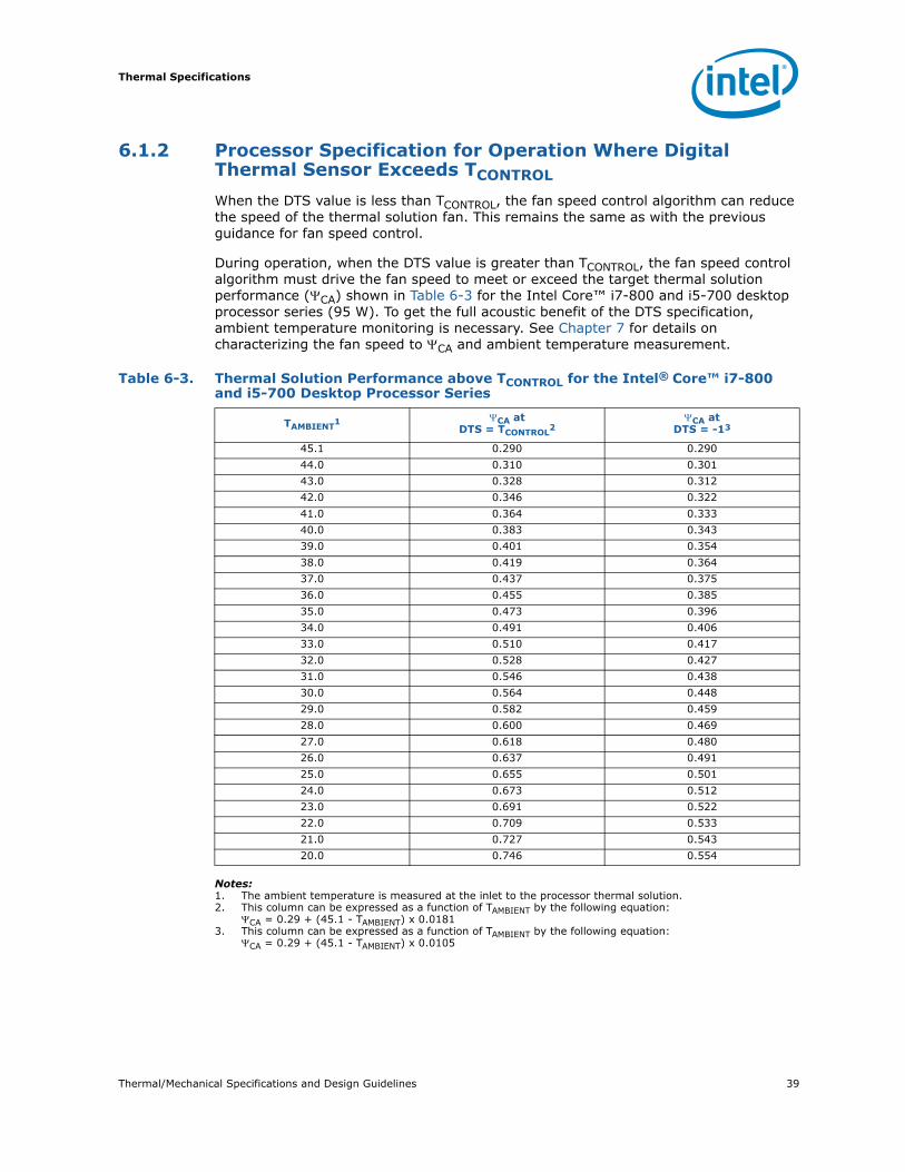
6.1.2 Processor Specification for Operation Where Digital Thermal Sensor Exceeds TCONTROL
When the DTS value is less than TCONTROL, the fan speed control algorithm can reduce the speed of the thermal solution fan. This remains the same as with the previous guidance for fan speed control.
During operation, when the DTS value is greater than TCONTROL, the fan speed control algorithm must drive the fan speed to meet or exceed the target thermal solution performance (ΨCA) shown in Table 6-3 for the Intel Core™ i7-800 and i5-700 desktop processor series (95 W). To get the full acoustic benefit of the DTS specification, ambient temperature monitoring is necessary. See Chapter 7 for details on characterizing the fan speed to ΨCA and ambient temperature measurement.
Notes:1. The ambient temperature is measured at the inlet to the processor thermal solution.2. This column can be expressed as a function of TAMBIENT by the following equation:
ΨCA = 0.29 + (45.1 - TAMBIENT) x 0.01813. This column can be expressed as a function of TAMBIENT by the following equation:
ΨCA = 0.29 + (45.1 - TAMBIENT) x 0.0105
Table 6-3. Thermal Solution Performance above TCONTROL for the Intel® Core™ i7-800 and i5-700 Desktop Processor Series
TAMBIENT1 ΨCA at
DTS = TCONTROL2
ΨCA at DTS = -13
45.1 0.290 0.290
44.0 0.310 0.301
43.0 0.328 0.312
42.0 0.346 0.322
41.0 0.364 0.333
40.0 0.383 0.343
39.0 0.401 0.354
38.0 0.419 0.364
37.0 0.437 0.375
36.0 0.455 0.385
35.0 0.473 0.396
34.0 0.491 0.406
33.0 0.510 0.417
32.0 0.528 0.427
31.0 0.546 0.438
30.0 0.564 0.448
29.0 0.582 0.459
28.0 0.600 0.469
27.0 0.618 0.480
26.0 0.637 0.491
25.0 0.655 0.501
24.0 0.673 0.512
23.0 0.691 0.522
22.0 0.709 0.533
21.0 0.727 0.543
20.0 0.746 0.554
Thermal Specifications
40 Thermal/Mechanical Specifications and Design Guidelines
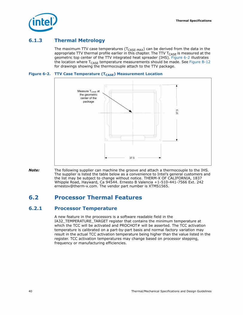
6.1.3 Thermal Metrology
The maximum TTV case temperatures (TCASE-MAX) can be derived from the data in the appropriate TTV thermal profile earlier in this chapter. The TTV TCASE is measured at the geometric top center of the TTV integrated heat spreader (IHS). Figure 6-2 illustrates the location where TCASE temperature measurements should be made. See Figure B-12 for drawings showing the thermocouple attach to the TTV package.
Note: The following supplier can machine the groove and attach a thermocouple to the IHS. The supplier is listed the table below as a convenience to Intel’s general customers and the list may be subject to change without notice. THERM-X OF CALIFORNIA, 1837 Whipple Road, Hayward, Ca 94544. Ernesto B Valencia +1-510-441-7566 Ext. 242 [email protected]. The vendor part number is XTMS1565.
6.2 Processor Thermal Features
6.2.1 Processor Temperature
A new feature in the processors is a software readable field in the IA32_TEMPERATURE_TARGET register that contains the minimum temperature at which the TCC will be activated and PROCHOT# will be asserted. The TCC activation temperature is calibrated on a part-by-part basis and normal factory variation may result in the actual TCC activation temperature being higher than the value listed in the register. TCC activation temperatures may change based on processor stepping, frequency or manufacturing efficiencies.
Figure 6-2. TTV Case Temperature (TCASE) Measurement Location
37.5
37.
5
Measure TCASE at the geometric center of the
package
Thermal/Mechanical Specifications and Design Guidelines 41
Thermal Specifications
6.2.2 Adaptive Thermal Monitor
The Adaptive Thermal Monitor feature provides an enhanced method for controlling the processor temperature when the processor silicon exceeds the Thermal Control Circuit (TCC) activation temperature. Adaptive Thermal Monitor uses TCC activation to reduce processor power via a combination of methods. The first method (Frequency/VID control, similar to Intel® Thermal Monitor 2 (TM2) in previous generation processors) involves the processor reducing its operating frequency (using the core ratio multiplier) and input voltage (using the VID signals). This combination of lower frequency and VID results in a reduction of the processor power consumption. The second method (clock modulation, known as Intel® Thermal Monitor 1 or TM1 in previous generation processors) reduces power consumption by modulating (starting and stopping) the internal processor core clocks. The processor intelligently selects the appropriate TCC method to use on a dynamic basis. BIOS is not required to select a specific method (as with previous-generation processors supporting TM1 or TM2). The temperature at which Adaptive Thermal Monitor activates the Thermal Control Circuit is factory calibrated and is not user configurable. Snooping and interrupt processing are performed in the normal manner while the TCC is active.
When the TCC activation temperature is reached, the processor will initiate TM2 in attempt to reduce its temperature. If TM2 is unable to reduce the processor temperature then TM1 will be also be activated. TM1 and TM2 will work together (clocks will be modulated at the lowest frequency ratio) to reduce power dissipation and temperature.
With a properly designed and characterized thermal solution, it is anticipated that the TCC would only be activated for very short periods of time when running the most power intensive applications. The processor performance impact due to these brief periods of TCC activation is expected to be so minor that it would be immeasurable. An under-designed thermal solution that is not able to prevent excessive activation of the TCC in the anticipated ambient environment may cause a noticeable performance loss, and in some cases may result in a TCASE that exceeds the specified maximum temperature and may affect the long-term reliability of the processor. In addition, a thermal solution that is significantly under-designed may not be capable of cooling the processor even when the TCC is active continuously. Refer to the appropriate Thermal Mechanical Design Guidelines for information on designing a compliant thermal solution.
The Intel Thermal Monitor does not require any additional hardware, software drivers, or interrupt handling routines. The following sections provide more details on the different TCC mechanisms used by the processor.
6.2.2.1 Frequency/VID Control
When the Digital Temperature Sensor (DTS) reaches a value of 0 (DTS temperatures reported using PECI may not equal zero when PROCHOT# is activated, see Section 6.3 for further details), the TCC will be activated and the PROCHOT# signal will be asserted. This indicates the processors' temperature has met or exceeded the factory calibrated trip temperature and it will take action to reduce the temperature.
Upon activation of the TCC, the processor will stop the core clocks, reduce the core ratio multiplier by 1 ratio, and restart the clocks. All processor activity stops during this frequency transition that occurs within 2 us. Once the clocks have been restarted at the new lower frequency, processor activity resumes while the voltage requested by the VID lines is stepped down to the minimum possible for the particular frequency.
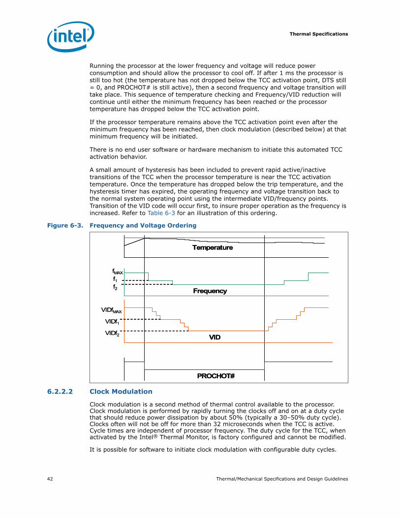
Thermal Specifications
42 Thermal/Mechanical Specifications and Design Guidelines
Running the processor at the lower frequency and voltage will reduce power consumption and should allow the processor to cool off. If after 1 ms the processor is still too hot (the temperature has not dropped below the TCC activation point, DTS still = 0, and PROCHOT# is still active), then a second frequency and voltage transition will take place. This sequence of temperature checking and Frequency/VID reduction will continue until either the minimum frequency has been reached or the processor temperature has dropped below the TCC activation point.
If the processor temperature remains above the TCC activation point even after the minimum frequency has been reached, then clock modulation (described below) at that minimum frequency will be initiated.
There is no end user software or hardware mechanism to initiate this automated TCC activation behavior.
A small amount of hysteresis has been included to prevent rapid active/inactive transitions of the TCC when the processor temperature is near the TCC activation temperature. Once the temperature has dropped below the trip temperature, and the hysteresis timer has expired, the operating frequency and voltage transition back to the normal system operating point using the intermediate VID/frequency points. Transition of the VID code will occur first, to insure proper operation as the frequency is increased. Refer to Table 6-3 for an illustration of this ordering.
6.2.2.2 Clock Modulation
Clock modulation is a second method of thermal control available to the processor. Clock modulation is performed by rapidly turning the clocks off and on at a duty cycle that should reduce power dissipation by about 50% (typically a 30–50% duty cycle). Clocks often will not be off for more than 32 microseconds when the TCC is active. Cycle times are independent of processor frequency. The duty cycle for the TCC, when activated by the Intel® Thermal Monitor, is factory configured and cannot be modified.
It is possible for software to initiate clock modulation with configurable duty cycles.
Figure 6-3. Frequency and Voltage Ordering
Temperature
fMAX
f1f2
VIDfMAX
VID
Frequency
VIDf2
VIDf1
PROCHOT#
Temperature
fMAX
f1f2
VIDfMAX
VID
Frequency
VIDf2
VIDf1
PROCHOT#
Thermal/Mechanical Specifications and Design Guidelines 43
Thermal Specifications
A small amount of hysteresis has been included to prevent rapid active/inactive transitions of the TCC when the processor temperature is near its maximum operating temperature. Once the temperature has dropped below the maximum operating temperature, and the hysteresis timer has expired, the TCC goes inactive and clock modulation ceases.
6.2.2.3 Immediate Transition to combined TM1 and TM2
As mentioned above, when the TCC is activated, the processor will sequentially step down the ratio multipliers and VIDs in an attempt to reduce the silicon temperature. If the temperature continues to increase and exceeds the TCC activation temperature by approximately 5 °C before the lowest ratio/VID combination has been reached, then the processor will immediately transition to the combined TM1/TM2 condition. The processor will remain in this state until the temperature has dropped below the TCC activation point. Once below the TCC activation temperature, TM1 will be discontinued and TM2 will be exited by stepping up to the appropriate ratio/VID state.
6.2.2.4 Critical Temperature Flag
If TM2 is unable to reduce the processor temperature, TM1 will also be activated. TM1 and TM2 will then work together to reduce power dissipation and temperature. It is expected that only a catastrophic thermal solution failure would create a situation where both TM1 and TM2 are active.
If TM1 and TM2 have both been active for greater than 20 ms and the processor temperature has not dropped below the TCC activation point, then the Critical Temperature Flag in the IA32_THERM_STATUS MSR will be set. This flag is an indicator of a catastrophic thermal solution failure and that the processor cannot reduce its temperature. Unless immediate action is taken to resolve the failure, the processor will probably reach the Thermtrip temperature (see Section 6.2.3 Thermtrip Signal) within a short time. In order to prevent possible permanent silicon damage, Intel recommends removing power from the processor within ½ second of the Critical Temperature Flag being set.
6.2.2.5 PROCHOT# Signal
An external signal, PROCHOT# (processor hot), is asserted when the processor core temperature has exceeded its specification. If Adaptive Thermal Monitor is enabled (note it must be enabled for the processor to be operating within specification), the TCC will be active when PROCHOT# is asserted.
The processor can be configured to generate an interrupt upon the assertion or de-assertion of PROCHOT#.
Although the PROCHOT# signal is an output by default, it may be configured as bi-directional. When configured in bi-directional mode, it is either an output indicating the processor has exceeded its TCC activation temperature or it can be driven from an external source (such as a voltage regulator) to activate the TCC. The ability to activate the TCC using PROCHOT# can provide a means for thermal protection of system components.
As an output, PROCHOT# (Processor Hot) will go active when the processor temperature monitoring sensor detects that one or more cores has reached its maximum safe operating temperature. This indicates that the processor Thermal Control Circuit (TCC) has been activated, if enabled. As an input, assertion of PROCHOT# by the system will activate the TCC for all cores. TCC activation when PROCHOT# is asserted by the system will result in the processor immediately
Thermal Specifications
44 Thermal/Mechanical Specifications and Design Guidelines
transitioning to the minimum frequency and corresponding voltage (using Freq/VID control). Clock modulation is not activated in this case. The TCC will remain active until the system de-asserts PROCHOT#.
Use of PROCHOT# in bi-directional mode can allow VR thermal designs to target maximum sustained current instead of maximum current. Systems should still provide proper cooling for the VR, and rely on PROCHOT# only as a backup in case of system cooling failure. The system thermal design should allow the power delivery circuitry to operate within its temperature specification even while the processor is operating at its Thermal Design Power.
6.2.3 THERMTRIP# Signal
Regardless of whether or not Adaptive Thermal Monitor is enabled, in the event of a catastrophic cooling failure, the processor will automatically shut down when the silicon has reached an elevated temperature. At this point, the THERMTRIP# signal will go active and stay active as described in the datasheet. THERMTRIP# activation is independent of processor activity. The temperature at which THERMTRIP# asserts is not user configurable and is not software visible.
6.3 Platform Environment Control Interface (PECI)
6.3.1 Introduction
The Platform Environment Control Interface (PECI) is a one-wire interface that provides a communication channel between Intel processor and chipset components to external monitoring devices. The processor implements a PECI interface to allow communication of processor thermal and other information to other devices on the platform. The processor provides a digital thermal sensor (DTS) for fan speed control. The DTS is calibrated at the factory to provide a digital representation of relative processor temperature. Instantaneous temperature readings from the DTS are available using the IA32_TEMPXXXX MSR; averaged DTS values are read using the PECI interface.
The PECI physical layer is a self-clocked one-wire bus that begins each bit with a driven, rising edge from an idle level near zero volts. The duration of the signal driven high depends on whether the bit value is a logic '0' or logic '1'. PECI also includes variable data transfer rate established with every message. The single wire interface provides low board routing overhead for the multiple load connections in the congested routing area near the processor and chipset components. Bus speed, error checking, and low protocol overhead provides adequate link bandwidth and reliability to transfer critical device operating conditions and configuration information.
The PECI bus offers:
• A wide speed range from 2 Kbps to 2 Mbps
• CRC check byte used to efficiently and automatically confirm accurate data delivery
• Synchronization at the beginning of every message minimizes device timing accuracy requirements.
Generic PECI specification details are out of the scope of this document. What follows is a processor-specific PECI client definition, and is largely an addendum to the PECI Network Layer and Design Recommendations sections for the PECI 2.0 specification document.
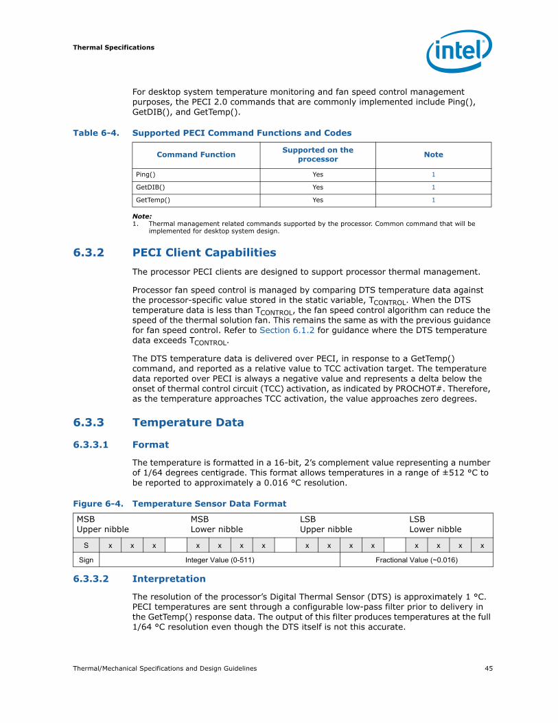
Thermal/Mechanical Specifications and Design Guidelines 45
Thermal Specifications
For desktop system temperature monitoring and fan speed control management purposes, the PECI 2.0 commands that are commonly implemented include Ping(), GetDIB(), and GetTemp().
Note:1. Thermal management related commands supported by the processor. Common command that will be
implemented for desktop system design.
6.3.2 PECI Client Capabilities
The processor PECI clients are designed to support processor thermal management.
Processor fan speed control is managed by comparing DTS temperature data against the processor-specific value stored in the static variable, TCONTROL. When the DTS temperature data is less than TCONTROL, the fan speed control algorithm can reduce the speed of the thermal solution fan. This remains the same as with the previous guidance for fan speed control. Refer to Section 6.1.2 for guidance where the DTS temperature data exceeds TCONTROL.
The DTS temperature data is delivered over PECI, in response to a GetTemp() command, and reported as a relative value to TCC activation target. The temperature data reported over PECI is always a negative value and represents a delta below the onset of thermal control circuit (TCC) activation, as indicated by PROCHOT#. Therefore, as the temperature approaches TCC activation, the value approaches zero degrees.
6.3.3 Temperature Data
6.3.3.1 Format
The temperature is formatted in a 16-bit, 2’s complement value representing a number of 1/64 degrees centigrade. This format allows temperatures in a range of ±512 °C to be reported to approximately a 0.016 °C resolution.
6.3.3.2 Interpretation
The resolution of the processor’s Digital Thermal Sensor (DTS) is approximately 1 °C. PECI temperatures are sent through a configurable low-pass filter prior to delivery in the GetTemp() response data. The output of this filter produces temperatures at the full 1/64 °C resolution even though the DTS itself is not this accurate.
Table 6-4. Supported PECI Command Functions and Codes
Command FunctionSupported on the
processorNote
Ping() Yes 1
GetDIB() Yes 1
GetTemp() Yes 1
Figure 6-4. Temperature Sensor Data Format
MSBUpper nibble
MSBLower nibble
LSBUpper nibble
LSBLower nibble
S x x x x x x x x x x x x x x x
Sign Integer Value (0-511) Fractional Value (~0.016)
Thermal Specifications
46 Thermal/Mechanical Specifications and Design Guidelines
Temperature readings from the processor are always negative in a 2’s complement format, and imply an offset from the reference TCC activation temperature. As an example, assume that the TCC activation temperature reference is 100 °C. A PECI thermal reading of -10 indicates that the processor is running at approximately 10 °C below the TCC activation temperature, or 90 °C. PECI temperature readings are not reliable at temperatures above TCC activation (since the processor is operating out of specification at this temperature). Therefore, the readings are never positive.
Note that changes in PECI data counts are approximately linear in relation to changes in temperature in degrees centigrade. A change of ‘1’ in the PECI count represents roughly a temperature change of 1 degree centigrade. This linearity is approximate and cannot be ensured over the entire range of PECI temperatures, especially as the delta from the maximum PECI temperature (zero) increases.
6.3.3.3 Processor Thermal Data Sample Rate and Filtering
The processor digital thermal sensor (DTS) provides an improved capability to monitor device hot spots, which inherently leads to more varying temperature readings over short time intervals. To reduce the sample rate requirements on PECI and improve thermal data stability versus time the processor DTS implements an averaging algorithm that filters the incoming data before reporting it over PECI.
6.3.3.4 Reserved Values
Several values well out of the operational range are reserved to signal temperature sensor errors. These are summarized in Table 6-5.
§
Table 6-5. Error Codes and Descriptions
Error Code Description
8000h General Sensor Error (GSE)
8002h Sensor is operational, but has detected a temperature below its operational range (underflow)
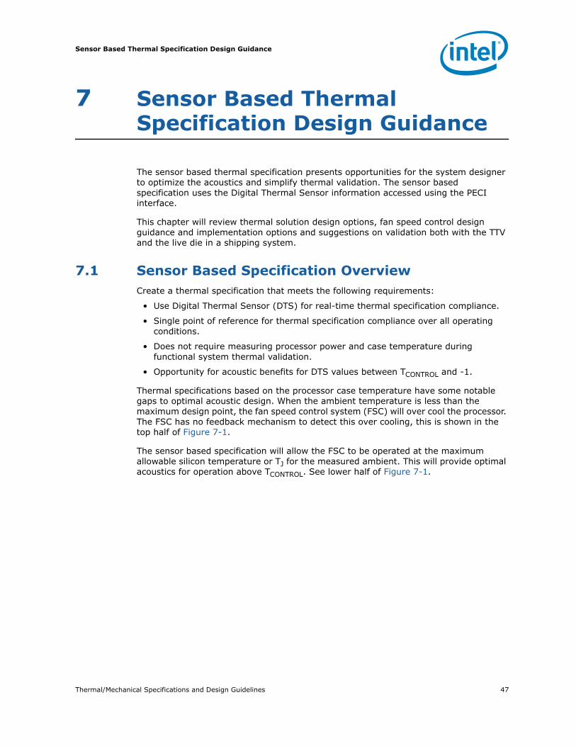
Thermal/Mechanical Specifications and Design Guidelines 47
Sensor Based Thermal Specification Design Guidance
7 Sensor Based Thermal Specification Design Guidance
The sensor based thermal specification presents opportunities for the system designer to optimize the acoustics and simplify thermal validation. The sensor based specification uses the Digital Thermal Sensor information accessed using the PECI interface.
This chapter will review thermal solution design options, fan speed control design guidance and implementation options and suggestions on validation both with the TTV and the live die in a shipping system.
7.1 Sensor Based Specification OverviewCreate a thermal specification that meets the following requirements:
• Use Digital Thermal Sensor (DTS) for real-time thermal specification compliance.
• Single point of reference for thermal specification compliance over all operating conditions.
• Does not require measuring processor power and case temperature during functional system thermal validation.
• Opportunity for acoustic benefits for DTS values between TCONTROL and -1.
Thermal specifications based on the processor case temperature have some notable gaps to optimal acoustic design. When the ambient temperature is less than the maximum design point, the fan speed control system (FSC) will over cool the processor. The FSC has no feedback mechanism to detect this over cooling, this is shown in the top half of Figure 7-1.
The sensor based specification will allow the FSC to be operated at the maximum allowable silicon temperature or TJ for the measured ambient. This will provide optimal acoustics for operation above TCONTROL. See lower half of Figure 7-1.
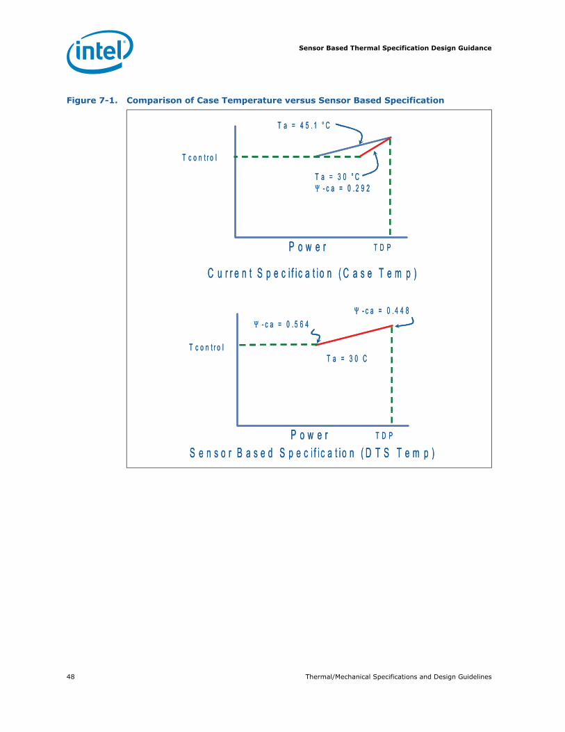
Sensor Based Thermal Specification Design Guidance
48 Thermal/Mechanical Specifications and Design Guidelines
Figure 7-1. Comparison of Case Temperature versus Sensor Based Specification
P o w e rS e n s o r B a s e d S p e c i f i c a t i o n ( D T S T e m p )
T D P
T c o n t r o lT a = 3 0 C
Ψ - c a = 0 . 5 6 4Ψ - c a = 0 . 4 4 8
P o w e r
C u r r e n t S p e c i f i c a t i o n ( C a s e T e m p )
T D P
T c o n t r o l
T a = 4 5 . 1 ° C
T a = 3 0 ° CΨ - c a = 0 . 2 9 2
P o w e rS e n s o r B a s e d S p e c i f i c a t i o n ( D T S T e m p )
T D P
T c o n t r o lT a = 3 0 C
Ψ - c a = 0 . 5 6 4Ψ - c a = 0 . 4 4 8
P o w e r
C u r r e n t S p e c i f i c a t i o n ( C a s e T e m p )
T D P
T c o n t r o l
T a = 4 5 . 1 ° C
T a = 3 0 ° CΨ - c a = 0 . 2 9 2
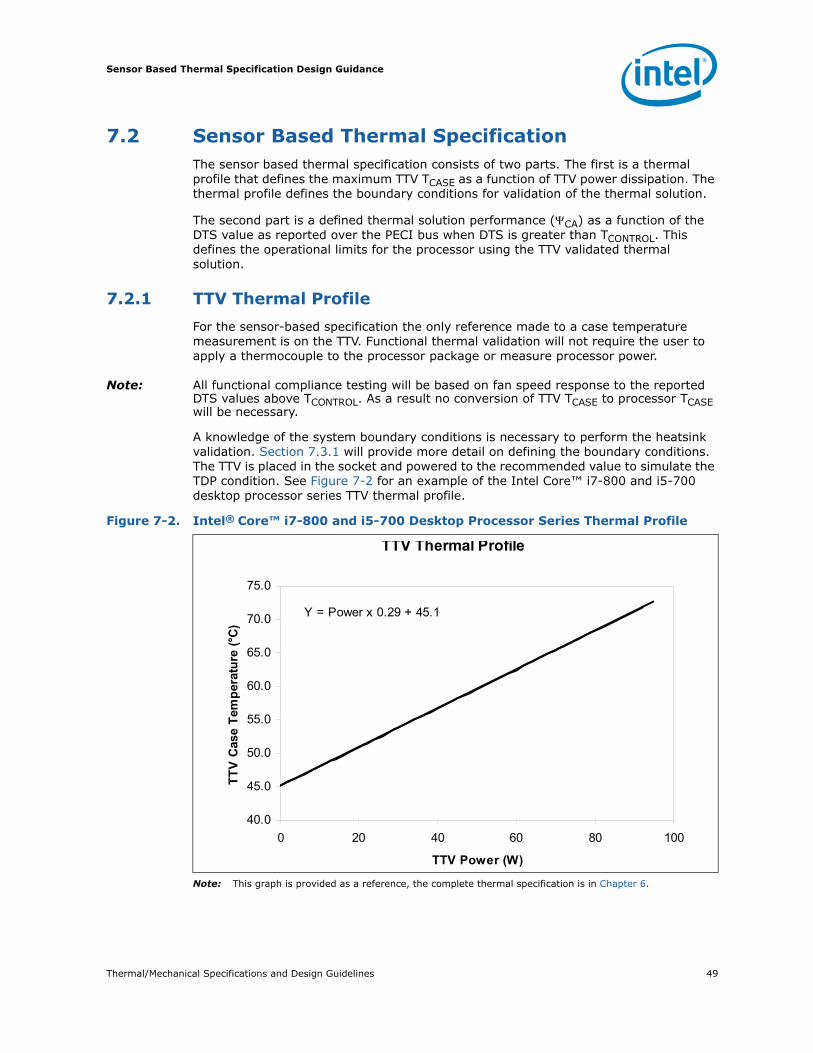
Thermal/Mechanical Specifications and Design Guidelines 49
Sensor Based Thermal Specification Design Guidance
7.2 Sensor Based Thermal SpecificationThe sensor based thermal specification consists of two parts. The first is a thermal profile that defines the maximum TTV TCASE as a function of TTV power dissipation. The thermal profile defines the boundary conditions for validation of the thermal solution.
The second part is a defined thermal solution performance (ΨCA) as a function of the DTS value as reported over the PECI bus when DTS is greater than TCONTROL. This defines the operational limits for the processor using the TTV validated thermal solution.
7.2.1 TTV Thermal Profile
For the sensor-based specification the only reference made to a case temperature measurement is on the TTV. Functional thermal validation will not require the user to apply a thermocouple to the processor package or measure processor power.
Note: All functional compliance testing will be based on fan speed response to the reported DTS values above TCONTROL. As a result no conversion of TTV TCASE to processor TCASE will be necessary.
A knowledge of the system boundary conditions is necessary to perform the heatsink validation. Section 7.3.1 will provide more detail on defining the boundary conditions. The TTV is placed in the socket and powered to the recommended value to simulate the TDP condition. See Figure 7-2 for an example of the Intel Core™ i7-800 and i5-700 desktop processor series TTV thermal profile.
Note: This graph is provided as a reference, the complete thermal specification is in Chapter 6.
Figure 7-2. Intel® Core™ i7-800 and i5-700 Desktop Processor Series Thermal Profile
TTV Thermal Profile
Y = Power x 0.29 + 45.1
40.0
45.0
50.0
55.0
60.0
65.0
70.0
75.0
0 20 40 60 80 100
TTV Power (W)
TTV
Cas
e Te
mpe
ratu
re (°
C)
Sensor Based Thermal Specification Design Guidance
50 Thermal/Mechanical Specifications and Design Guidelines
7.2.2 Specification When DTS value is Greater than TCONTROL
The product specification provides a table of ΨCA values at DTS = TCONTROL and DTS = -1 as a function of TAMBIENT (inlet to heatsink). Between these two defined points, a linear interpolation can be done for any DTS value reported by the processor. A copy of the specification is provided as a reference in Table 7-1 of Section 7.6.
The fan speed control algorithm has enough information using only the DTS value and TAMBIENT to command the thermal solution to provide just enough cooling to keep the part on the thermal profile.
As an example the data in Table 7-1 has been plotted in Figure 7-3 to show the required ΨCA at 25, 30, 35, and 40°C TAMBIENT. The lower the ambient, the higher the required ΨCA, which means lower fan speeds and reduced acoustics from the processor thermal solution.
In the prior thermal specifications this region, DTS values greater than TCONTROL, was defined by the processor thermal profile. This required the user to estimate the processor power and case temperature. Neither of these two data points are accessible in real time for the fan speed control system. As a result the designer had to assume the worst case TAMBIENT and drive the fans to accommodate that boundary condition.
Figure 7-3. Thermal solution Performance
0.300
0.350
0.400
0.450
0.500
0.550
0.600
0.650
0.700
DTS = Tcontrol DTS = -1
TTV
Thet
a_ca
[C/W
]
Ta = 40 °C
Ta = 35 °C
Ta = 30 °C
Ta = 25 °C
TTV Ψ_ca @ TTV Ψ_ca @
Thermal/Mechanical Specifications and Design Guidelines 51
Sensor Based Thermal Specification Design Guidance
7.3 Thermal Solution Design ProcessThermal solution design guidance for this specification is the same as with previous products. The initial design needs to take into account the target market and overall product requirements for the system. This can be broken down into several steps:
• Boundary condition definition
• Thermal design / modelling
• Thermal testing
7.3.1 Boundary Condition Definition
Using the knowledge of the system boundary conditions such as inlet air temperature, acoustic requirements, cost, design for manufacturing, package and socket mechanical specifications and chassis environmental test limits the designer can make informed thermal solution design decisions.
For the and Intel Core™ i7-800 and i5-700 desktop processor series, the thermal boundary conditions for an ATX tower system are as follows:
• TEXTERNAL = 35 °C. This is typical of a maximum system operating environment
• TRISE = 5 °C. This is typical of a chassis compliant to CAG 1.1 or TAC 2.0.
• TAMBIENT = 40 °C (TAMBIENT = TEXTERNAL + TRISE)
Based on the system boundary conditions the designer can select a TAMBIENT and ΨCA to use in thermal modelling. The assumption of a TAMBIENT has a significant impact on the required ΨCA needed to meet TTV TCASEMAX at TDP. A system that can deliver lower assumed TAMBIENT can utilize a design with a higher ΨCA, which can have a lower cost. Figure 7-4 shows a number of satisfactory solutions for the Intel Core™ i7-800 and i5-700 desktop processor series.
Note: If the assumed TAMBIENT is inappropriate for the intended system environment, the thermal solution performance may not be sufficient to meet the product requirements. The results may be excessive noise from fans having to operate at a speed higher than intended. In the worst case this can lead to performance loss with excessive activation of the Thermal Control Circuit (TCC).
Sensor Based Thermal Specification Design Guidance
52 Thermal/Mechanical Specifications and Design Guidelines
Note: If an ambient of greater than 45.1 °C is necessary based on the boundary conditions a thermal solution with a ΨCA lower than 0.29 °C/W will be required.
7.3.2 Thermal Design and Modelling
Based on the boundary conditions the designer can now make the design selection of the thermal solution components. The major components that can be mixed are the fan, fin geometry, heat pipe or air cooled solid core design. There are cost and acoustic trade-offs the customer can make.
7.3.3 Thermal Solution Validation
7.3.3.1 Test for Compliance with the TTV Thermal Profile
This step is the same as previously suggested for prior products. The thermal solution is mounted on a test fixture with the TTV and tested at the following conditions:
• TTV is powered to the TDP condition
• Thermal solution fan operating at full speed
• TAMBIENT at the boundary condition from Section 7.3.1
The following data is collected: TTV power, TTV TCASE, and TAMBIENT. This is used to calculate ΨCA which is defined as:
ΨCA = (TTV TCASE – TAMBIENT) / Power
This testing is best conducted on a bench to eliminate as many variables as possible when assessing the thermal solution performance. The boundary condition analysis as described in Section 7.3.1 should help in making the bench test simpler to perform.
Figure 7-4. Required ΨCA for Various TAMBIENT Conditions
0.0
10.0
20.0
30.0
40.0
50.0
60.0
70.0
80.0
0 20 40 60 80
TTV Power Dissipation (W)
TTV
Tca
se (°
C)
Ψ-ca = 0.45 Ta = 30 °C
Ψ-ca = 0.40 Ta = 35 °C
Ψ-ca = 0.34 Ta = 40 °C
Ψ-ca = 0.29 Ta = 45.1 °C
Thermal/Mechanical Specifications and Design Guidelines 53
Sensor Based Thermal Specification Design Guidance
7.3.3.2 Thermal Solution Characterization for Fan Speed Control
The final step in thermal solution validation is to establish the thermal solution performance,ΨCA and acoustics as a function of fan speed. This data is necessary to allow the fan speed control algorithm developer to program the device. It also is needed to asses the expected acoustic impact of the processor thermal solution in the system.
The characterization data should be taken over the operating range of the fan. Using the RCBF7-1156 (DHA-A) as the example the fan is operational from 900 to 3150 RPM. The data was collected at several points and a curve was fit to the data see Figure 7-5. Taking data at 6 evenly distributed fan speeds over the operating range should provide enough data to establish an equation. By using the equation from the curve fitting a complete set of required fan speeds as a function of ΨCA be developed. The results from the reference thermal solution characterization are provided in Table 7-1.
The fan speed control device may modulate the thermal solution fan speed (RPM) by one of two methods. The first and preferred is pulse width modulation (PWM) signal compliant with the 4-Wire Pulse Width Modulation (PWM) Controlled Fans specification. the alternative is varying the input voltage to the fan. As a result the characterization data needs to also correlate the RPM to PWM or voltage to the thermal solution fan. The fan speed algorithm developer needs to associate the output command from the fan speed control device with the required thermal solution performance as stated in Table 7-1. Regardless of which control method is used, the term RPM will be used to indicate required fan speed in the rest of this document.
Note: When selecting a thermal solution from a thermal vendor, the characterization data should be requested directly from them as a part of their thermal solution collateral.
Note: This data is taken from the preliminary evaluation of the validation of the RCBF7-1156 (DHA-A) reference processor thermal solution. The ΨCA versus RPM data is available in Table 7-1 at the end of this chapter.
Figure 7-5. Thermal Solution Performance versus Fan Speed
Sensor Based Thermal Specification Design Guidance
54 Thermal/Mechanical Specifications and Design Guidelines
7.4 Fan Speed Control (FSC) design processThe next step is to incorporate the thermal solution characterization data into the algorithms for the device controlling the fans.
As a reminder, the requirements are:
• When the DTS value is at or below TCONTROL, the fans can be slowed down — just as with prior processors.
• When DTS is above TCONTROL, FSC algorithms will use knowledge of TAMBIENT and ΨCA versus RPM to achieve the necessary level of cooling.
This chapter will discuss two implementations. The first is a FSC system that is not provided the TAMBIENT information and a FSC system that is provided data on the current TAMBIENT. Either method will result in a thermally compliant solution and some acoustic benefit by operating the processor closer to the thermal profile. But only the TAMBIENT aware FSC system can fully use the specification for optimized acoustic performance.
In the development of the FSC algorithm it should be noted that the TAMBIENT is expected to change at a significantly slower rate than the DTS value. The DTS value will be driven by the workload on the processor and the thermal solution will be required to respond to this much more rapidly than the changes in TAMBIENT.
An additional consideration in establishing the fan speed curves is to account for the thermal interface material performance degradation over time.
7.4.1 Fan Speed Control Algorithm without TAMBIENT Data
In a system that does not provide the FSC algorithm with the TAMBIENT information, the designer must make the following assumption:
• When the DTS value is greater than TCONTROL, the TAMBIENT is at boundary condition derived in Section 7.3.1.
This is consistent past FSC guidance from Intel, to accelerate the fan to full speed when the DTS value is greater than TCONTROL. As will be shown below, the DTS thermal specification at DTS = TCONTROL can reduce some of the over cooling of the processor and provide an acoustic noise reduction from the processor thermal solution.
In this example the following assumptions are made:
• TAMBIENT = 40 °C
• Thermal Solution designed / validated to a 40 °C environment
• TCONTROL = -20
• Reference processor thermal solution (RCFH7-1156 (DHA-A))
• Below TCONTROL the fan speed is slowed down as in prior products
For a processor specification based on a TCASE thermal profile, when the DTS value is equal to or greater than TCONTROL, the fan speed must be accelerated to full speed. For the reference thermal solution full speed is 3150 RPM (dashed line in Figure 7-6). The DTS thermal specification defines a required ΨCA at TCONTROL and the fan speed is 2300 RPM. This is much less than full speed even when assuming the TAMBIENT = 40 °C (solid line in Figure 7-6). The shaded area displayed in Figure 7-6 is where DTS values
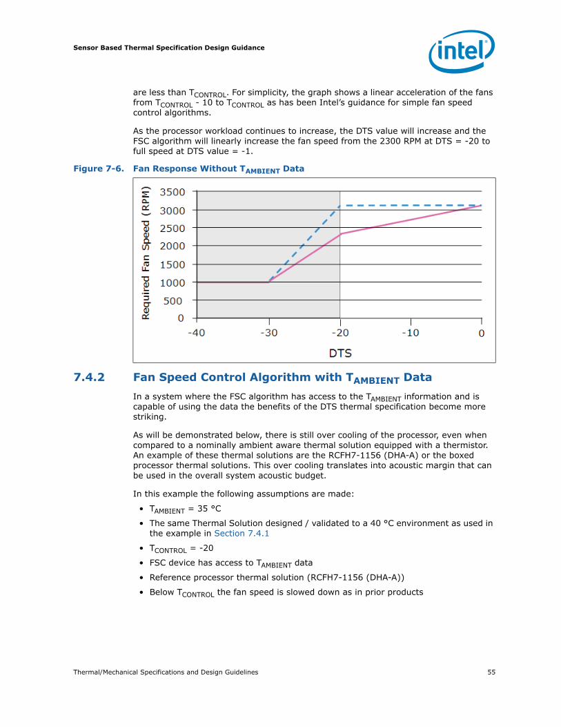
Thermal/Mechanical Specifications and Design Guidelines 55
Sensor Based Thermal Specification Design Guidance
are less than TCONTROL. For simplicity, the graph shows a linear acceleration of the fans from TCONTROL - 10 to TCONTROL as has been Intel’s guidance for simple fan speed control algorithms.
As the processor workload continues to increase, the DTS value will increase and the FSC algorithm will linearly increase the fan speed from the 2300 RPM at DTS = -20 to full speed at DTS value = -1.
7.4.2 Fan Speed Control Algorithm with TAMBIENT Data
In a system where the FSC algorithm has access to the TAMBIENT information and is capable of using the data the benefits of the DTS thermal specification become more striking.
As will be demonstrated below, there is still over cooling of the processor, even when compared to a nominally ambient aware thermal solution equipped with a thermistor. An example of these thermal solutions are the RCFH7-1156 (DHA-A) or the boxed processor thermal solutions. This over cooling translates into acoustic margin that can be used in the overall system acoustic budget.
In this example the following assumptions are made:
• TAMBIENT = 35 °C
• The same Thermal Solution designed / validated to a 40 °C environment as used in the example in Section 7.4.1
• TCONTROL = -20
• FSC device has access to TAMBIENT data
• Reference processor thermal solution (RCFH7-1156 (DHA-A))
• Below TCONTROL the fan speed is slowed down as in prior products
Figure 7-6. Fan Response Without TAMBIENT Data

Sensor Based Thermal Specification Design Guidance
56 Thermal/Mechanical Specifications and Design Guidelines
For a processor specification based on a TCASE thermal profile, when the DTS value is equal to or greater than TCONTROL, the fan speed is accelerated to maximum fan speed for the TAMBIENT as controlled by the thermistor in thermal solution. For the RCFH7-1156 (DHA-A), this would be about 2150 RPM at 35 °C. This is graphically displayed as the dashed line in Figure 7-7.
This is an improvement over the ambient unaware system but is not fully optimized for acoustic benefit. The DTS thermal specification required ΨCA and therefore the fan speed in this scenario is 1500 RPM. This is less than thermistor controlled speed of 2150 RPM — even if the assumption is a TAMBIENT = 35 °C. This is graphically displayed in Figure 7-7.
The shaded area displayed in Figure 7-7 is where DTS values are less than TCONTROL. For simplicity, the graph shows a linear acceleration of the fans from TCONTROL - 10 to TCONTROL as has been Intel’s guidance for simple fan speed control algorithms.
As the processor workload continues to increase the DTS value will increase and the FSC algorithm will linearly increase the fan speed from the 1500 RPM at DTS = -20 to 2150 RPM at DTS value = -1.
Figure 7-7. Fan Response with TAMBIENT Aware FSC
Thermal/Mechanical Specifications and Design Guidelines 57
Sensor Based Thermal Specification Design Guidance
7.5 System ValidationSystem validation should focus on ensuring the fan speed control algorithm is responding appropriately to the DTS values and TAMBIENT data as well as any other device being monitored for thermal compliance.
Since the processor thermal solution has already been validated using the TTV to the thermal specifications at the predicted TAMBIENT, additional TTV based testing in the chassis is not expected to be necessary.
Once the heatsink has been demonstrated to meet the TTV Thermal Profile, it should be evaluated on a functional system at the boundary conditions.
In the system under test and Power/Thermal Utility Software set to dissipate the TDP workload confirm the following item:
• Verify if there is TCC activity by instrumenting the PROCHOT# signal from the processor. TCC activation in functional application testing is unlikely with a compliant thermal solution. Some very high power applications might activate TCC for short intervals this is normal.
• Verify fan speed response is within expectations — actual RPM (ΨCA) is consistent with DTS temperature and TAMBIENT.
• Verify RPM versus PWM command (or voltage) output from the FSC device is within expectations.
• Perform sensitivity analysis to asses impact on processor thermal solution performance and acoustics for the following:— Other fans in the system.— Other thermal loads in the system.
In the same system under test, run real applications that are representative of the expected end user usage model and verify the following:
• Verify fan speed response vs. expectations as done using Power/Thermal Utility SW• Validate system boundary condition assumptions: Trise, venting locations, other
thermal loads and adjust models / design as required.
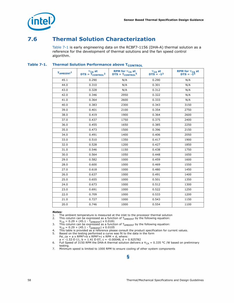
Sensor Based Thermal Specification Design Guidance
58 Thermal/Mechanical Specifications and Design Guidelines
7.6 Thermal Solution Characterization Table 7-1 is early engineering data on the RCBF7-1156 (DHA-A) thermal solution as a reference for the development of thermal solutions and the fan speed control algorithm.
Notes:1. The ambient temperature is measured at the inlet to the processor thermal solution2. This column can be expressed as a function of TAMBIENT by the following equation:
ΨCA = 0.29 + (45.1 - TAMBIENT) x 0.01813. This column can be expressed as a function of TAMBIENT by the following equation:
ΨCA = 0.29 + (45.1 - TAMBIENT) x 0.01054. This table is provided as a reference please consult the product specification for current values.5. Based on the testing performed a curve was fit to the data in the form
Psi_ca = a x RPM3+b x RPM2+c x RPM + d, where:a = -1.53 E-11, b = 1.41 E-07, c = -0.00048, d = 0.925782
6. Full Speed of 3150 RPM the DHA-A thermal solution delivers a ΨCA = 0.335 °C /W based on preliminary testing.
7. Minimum speed is limited to 1000 RPM to ensure cooling of other system components
§
Table 7-1. Thermal Solution Performance above TCONTROL
TAMBIENT1 ΨCA at
DTS = TCONTROL2
RPM for ΨCA at DTS = TCONTROL
5ΨCA at
DTS = -13RPM for ΨCA at
DTS = -15
45.1 0.290 N/A 0.290 N/A
44.0 0.310 N/A 0.301 N/A
43.0 0.328 N/A 0.312 N/A
42.0 0.346 2950 0.322 N/A
41.0 0.364 2600 0.333 N/A
40.0 0.383 2300 0.343 3150
39.0 0.401 2100 0.354 2750
38.0 0.419 1900 0.364 2600
37.0 0.437 1750 0.375 2400
36.0 0.455 1650 0.385 2250
35.0 0.473 1500 0.396 2150
34.0 0.491 1400 0.406 2050
33.0 0.510 1350 0.417 1900
32.0 0.528 1200 0.427 1850
31.0 0.546 1150 0.438 1750
30.0 0.564 1050 0.448 1650
29.0 0.582 1000 0.459 1600
28.0 0.600 1000 0.469 1550
27.0 0.618 1000 0.480 1450
26.0 0.637 1000 0.491 1400
25.0 0.655 1000 0.501 1350
24.0 0.673 1000 0.512 1300
23.0 0.691 1000 0.522 1250
22.0 0.709 1000 0.533 1200
21.0 0.727 1000 0.543 1150
20.0 0.746 1000 0.554 1100

Thermal/Mechanical Specifications and Design Guidelines 59
ATX Reference Thermal Solution
8 ATX Reference Thermal Solution
Note: The reference thermal mechanical solution information shown in this document represents the current state of the data and may be subject to modification.The information represents design targets, not commitments by Intel.
The design strategy is to use the design concepts from the prior Intel® Radial Curved Bifurcated Fin Heatsink Reference Design (Intel® RCBFH Reference Design) designed originally for the Intel® Pentium® 4 processors.
This chapter describes the overall requirements for the ATX heatsink reference thermal solution supporting the processors including critical-to-function dimensions, operating environment, and validation criteria.
.
8.1 Heatsink Thermal SolutionThe reference thermal solutions are active fan solution similar to the prior designs for the Intel® Pentium® 4 and Intel® Core™2 Duo processors. The RCFH7-1156 (DHA-A) is a universal design supporting the Intel® Core™ i7-800 and i5-700 desktop processor series processors.
Figure 8-1 shows the reference thermal solution assembly. The heat sink attaches to the motherboard with the push pin fastener design from previous reference designs, see Figure B-6 through Figure B-9 for details on the push pin fastener design.
Table 8-1. Reference Thermal Solutions
Thermal Solution Name Guidelines Processor
RCFH7-1156 (DHA-A) 2009B (09B) Intel® Core™ i7-800 and i5-700 desktop processor series (95W)
Figure 8-1. ATX Heatsink Reference Design Assembly
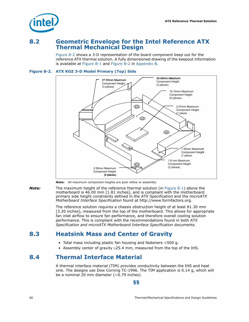
ATX Reference Thermal Solution
60 Thermal/Mechanical Specifications and Design Guidelines
8.2 Geometric Envelope for the Intel Reference ATX Thermal Mechanical DesignFigure 8-2 shows a 3-D representation of the board component keep out for the reference ATX thermal solution. A fully dimensioned drawing of the keepout information is available at Figure B-1 and Figure B-2 in Appendix B.
Note: All maximum component heights are post reflow or assembly.
Note: The maximum height of the reference thermal solution (in Figure 8-1) above the motherboard is 46.00 mm [1.81 inches], and is compliant with the motherboard primary side height constraints defined in the ATX Specification and the microATX Motherboard Interface Specification found at http://www.formfactors.org.
The reference solution requires a chassis obstruction height of at least 81.30 mm [3.20 inches], measured from the top of the motherboard. This allows for appropriate fan inlet airflow to ensure fan performance, and therefore overall cooling solution performance. This is compliant with the recommendations found in both ATX Specification and microATX Motherboard Interface Specification documents.
8.3 Heatsink Mass and Center of Gravity• Total mass including plastic fan housing and fasteners <500 g.• Assembly center of gravity ≤25.4 mm, measured from the top of the IHS.
8.4 Thermal Interface MaterialA thermal interface material (TIM) provides conductivity between the IHS and heat sink. The designs use Dow Corning TC-1996. The TIM application is 0.14 g, which will be a nominal 20 mm diameter (~0.79 inches).
§§
Figure 8-2. ATX KOZ 3-D Model Primary (Top) Side
27.00mm Maximum Component Height(3 places)
10.10mm Maximum Component Height(5 places)
2.07mm Maximum Component Height(1 place)
1.20mm Maximum Component Height(1 place)
2.50mm Maximum Component Height
(6 places)
26.00mm Maximum Component Height(3 places)
1.6 mm Maximum Component Height(2 places)
27.00mm Maximum Component Height(3 places)
10.10mm Maximum Component Height(5 places)
2.07mm Maximum Component Height(1 place)
1.20mm Maximum Component Height(1 place)
2.50mm Maximum Component Height
(6 places)
26.00mm Maximum Component Height(3 places)
1.6 mm Maximum Component Height(2 places)
Thermal/Mechanical Specifications and Design Guidelines 61
Thermal Solution Quality and Reliability Requirements
9 Thermal Solution Quality and Reliability Requirements
9.1 Reference Heatsink Thermal VerificationEach motherboard, heatsink and attach combination may vary the mechanical loading of the component. Based on the end user environment, the user should define the appropriate reliability test criteria and carefully evaluate the completed assembly prior to use in high volume. The Intel reference thermal solution will be evaluated to the boundary conditions in Chapter 5.
The test results, for a number of samples, are reported in terms of a worst-case mean + 3σ value for thermal characterization parameter using the TTV.
9.2 Mechanical Environmental TestingEach motherboard, heatsink and attach combination may vary the mechanical loading of the component. Based on the end user environment, the user should define the appropriate reliability test criteria and carefully evaluate the completed assembly prior to use in high volume. Some general recommendations are shown in Table 9-1.
The Intel reference heatsinks will be tested in an assembled LGA1156 socket and mechanical test package. Details of the environmental requirements, and associated stress tests, can be found in Table 9-1 are based on speculative use condition assumptions, and are provided as examples only.
Notes:1. It is recommended that the above tests be performed on a sample size of at least ten assemblies from
multiple lots of material.2. Additional pass/fail criteria may be added at the discretion of the user.
Table 9-1. Use Conditions (Board Level)
Test1 Requirement Pass/Fail Criteria2
Mechanical Shock
3 drops each for + and - directions in each of 3 perpendicular axes (i.e., total 18 drops)Profile: 50 g, Trapezoidal waveform, 4.3 m/s [170 in/s] minimum velocity change
Visual Check and Electrical Functional Test
Random Vibration
Duration: 10 min/axis, 3 axesFrequency Range: 5 Hz to 500 Hz 5 Hz @ 0.01 g2/Hz to 20 Hz @ 0.02 g2/Hz (slope up)20 Hz to 500 Hz @ 0.02 g2/Hz (flat)Power Spectral Density (PSD) Profile: 3.13 g RMS
Visual Check and Electrical Functional Test
Thermal Solution Quality and Reliability Requirements
62 Thermal/Mechanical Specifications and Design Guidelines
9.2.1 Recommended Test Sequence
Each test sequence should start with components (that is, baseboard, heatsink assembly, and so forth) that have not been previously submitted to any reliability testing.
Prior to the mechanical shock & vibration test, the units under test should be preconditioned for 72 hours at 45 ºC. The purpose is to account for load relaxation during burn-in stage.
The test sequence should always start with a visual inspection after assembly, and BIOS/Processor/memory test. The stress test should be then followed by a visual inspection and then BIOS/Processor/memory test.
9.2.2 Post-Test Pass Criteria
The post-test pass criteria are:
1. No significant physical damage to the heatsink and retention hardware.
2. Heatsink remains seated and its bottom remains mated flatly against the IHS surface. No visible gap between the heatsink base and processor IHS. No visible tilt of the heatsink with respect to the retention hardware.
3. No signs of physical damage on baseboard surface due to impact of heatsink.
4. No visible physical damage to the processor package.
5. Successful BIOS/Processor/memory test of post-test samples.
6. Thermal compliance testing to demonstrate that the case temperature specification can be met.
9.2.3 Recommended BIOS/Processor/Memory Test Procedures
This test is to ensure proper operation of the product before and after environmental stresses, with the thermal mechanical enabling components assembled. The test shall be conducted on a fully operational baseboard that has not been exposed to any battery of tests prior to the test being considered.
Testing setup should include the following components, properly assembled and/or connected:
• Appropriate system baseboard.
• Processor and memory.
• All enabling components, including socket and thermal solution parts.
The pass criterion is that the system under test shall successfully complete the checking of BIOS, basic processor functions and memory, without any errors. Intel PC Diags is an example of software that can be used for this test.
Thermal/Mechanical Specifications and Design Guidelines 63
Thermal Solution Quality and Reliability Requirements
9.3 Material and Recycling RequirementsMaterial shall be resistant to fungal growth. Examples of non-resistant materials include cellulose materials, animal and vegetable based adhesives, grease, oils, and many hydrocarbons. Synthetic materials such as PVC formulations, certain polyurethane compositions (such as polyester and some polyethers), plastics that contain organic fillers of laminating materials, paints, and varnishes also are susceptible to fungal growth. If materials are not fungal growth resistant, then MIL-STD-810E, Method 508.4 must be performed to determine material performance.
Material used shall not have deformation or degradation in a temperature life test.
Any plastic component exceeding 25 grams should be recyclable per the European Blue Angel recycling standards.
The following definitions apply to the use of the terms lead-free, Pb-free, and RoHS compliant.
Lead (Pb)-free: Lead has not been intentionally added, but lead may still exist as an impurity below 1000 ppm.
RoHS compliant: Lead and other materials banned in RoHS Directive are either (1) below all applicable substance thresholds as proposed by the EU or (2) an approved/pending exemption applies.
Note: RoHS implementation details are not fully defined and may change.
§

Thermal Solution Quality and Reliability Requirements
64 Thermal/Mechanical Specifications and Design Guidelines
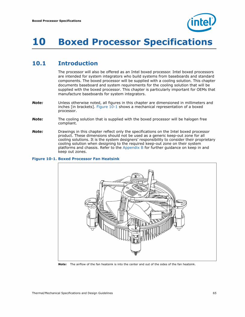
Thermal/Mechanical Specifications and Design Guidelines 65
Boxed Processor Specifications
10 Boxed Processor Specifications
10.1 IntroductionThe processor will also be offered as an Intel boxed processor. Intel boxed processors are intended for system integrators who build systems from baseboards and standard components. The boxed processor will be supplied with a cooling solution. This chapter documents baseboard and system requirements for the cooling solution that will be supplied with the boxed processor. This chapter is particularly important for OEMs that manufacture baseboards for system integrators.
Note: Unless otherwise noted, all figures in this chapter are dimensioned in millimeters and inches [in brackets]. Figure 10-1 shows a mechanical representation of a boxed processor.
Note: The cooling solution that is supplied with the boxed processor will be halogen free compliant.
Note: Drawings in this chapter reflect only the specifications on the Intel boxed processor product. These dimensions should not be used as a generic keep-out zone for all cooling solutions. It is the system designers’ responsibility to consider their proprietary cooling solution when designing to the required keep-out zone on their system platforms and chassis. Refer to the Appendix B for further guidance on keep in and keep out zones.
Note: The airflow of the fan heatsink is into the center and out of the sides of the fan heatsink.
Figure 10-1. Boxed Processor Fan Heatsink

Boxed Processor Specifications
66 Thermal/Mechanical Specifications and Design Guidelines
10.2 Mechanical Specifications
10.2.1 Boxed Processor Cooling Solution Dimensions
This section documents the mechanical specifications of the boxed processor. The boxed processor will be shipped with an unattached fan heatsink. Figure 10-1 shows a boxed processor fan heatsink.
Clearance is required around the fan heatsink to ensure unimpeded airflow for proper cooling. The physical space requirements and dimensions for the boxed processor with assembled fan heatsink are shown in Figure 10-2 (side view), and Figure 10-3 (top view). The airspace requirements for the boxed processor fan heatsink must also be incorporated into new baseboard and system designs. Airspace requirements are shown in Figure 10-7 and Figure 10-8. Note that some figures have centerlines shown (marked with alphabetic designations) to clarify relative dimensioning.
Figure 10-2. Space Requirements for the Boxed Processor (side view)
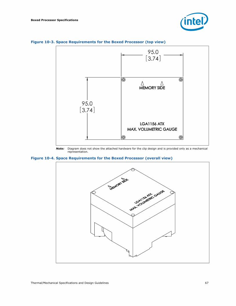
Thermal/Mechanical Specifications and Design Guidelines 67
Boxed Processor Specifications
Note: Diagram does not show the attached hardware for the clip design and is provided only as a mechanical representation.
Figure 10-3. Space Requirements for the Boxed Processor (top view)
Figure 10-4. Space Requirements for the Boxed Processor (overall view)

Boxed Processor Specifications
68 Thermal/Mechanical Specifications and Design Guidelines
10.2.2 Boxed Processor Fan Heatsink Weight
The boxed processor fan heatsink will not weigh more than 450 grams.
10.2.3 Boxed Processor Retention Mechanism and Heatsink Attach Clip Assembly
The boxed processor thermal solution requires a heatsink attach clip assembly, to secure the processor and fan heatsink in the baseboard socket. The boxed processor will ship with the heatsink attach clip assembly.
10.3 Electrical Requirements
10.3.1 Fan Heatsink Power Supply
The boxed processor's fan heatsink requires a +12 V power supply. A fan power cable will be shipped with the boxed processor to draw power from a power header on the baseboard. The power cable connector and pinout are shown in Figure 10-5. Baseboards must provide a matched power header to support the boxed processor. Table 10-1 contains specifications for the input and output signals at the fan heatsink connector.
The fan heatsink outputs a SENSE signal, which is an open-collector output that pulses at a rate of 2 pulses per fan revolution. A baseboard pull-up resistor provides VOH to match the system board-mounted fan speed monitor requirements, if applicable. Use of the SENSE signal is optional. If the SENSE signal is not used, pin 3 of the connector should be tied to GND.
The fan heatsink receives a PWM signal from the motherboard from the 4th pin of the connector labeled as CONTROL.
The boxed processor's fanheat sink requires a constant +12 V supplied to pin 2 and does not support variable voltage control or 3-pin PWM control.
The power header on the baseboard must be positioned to allow the fan heatsink power cable to reach it. The power header identification and location should be documented in the platform documentation, or on the system board itself. Figure 10-6 shows the location of the fan power connector relative to the processor socket. The baseboard power header should be positioned within 110 mm [4.33 inches] from the center of the processor socket.
Figure 10-5. Boxed Processor Fan Heatsink Power Cable Connector Description
Pin Signal
1 2 3 4
1234
GND+12 VSENSECONTROL
Straight square pin, 4-pin terminal housing withpolarizing ribs and friction locking ramp.
0.100" pitch, 0.025" square pin width.
Match with straight pin, friction lock header onmainboard.

Thermal/Mechanical Specifications and Design Guidelines 69
Boxed Processor Specifications
10.4 Thermal SpecificationsThis section describes the cooling requirements of the fan heatsink solution used by the boxed processor.
10.4.1 Boxed Processor Cooling Requirements
The boxed processor may be directly cooled with a fan heatsink. However, meeting the processor's temperature specification is also a function of the thermal design of the entire system, and ultimately the responsibility of the system integrator. The processor temperature specification is found in Chapter 6 of this document. The boxed processor fan heatsink is able to keep the processor temperature within the specifications (see Table 6.1) in chassis that provide good thermal management. For the boxed processor fan heatsink to operate properly, it is critical that the airflow provided to the fan heatsink is unimpeded. Airflow of the fan heatsink is into the center and out of the sides of the fan heatsink. Airspace is required around the fan to ensure that the airflow through the fan heatsink is not blocked. Blocking the airflow to the fan heatsink reduces the cooling efficiency and decreases fan life. Figure 10-7 and Figure 10-8 illustrate an acceptable airspace clearance for the fan heatsink. The air temperature entering the fan should be kept below 40 ºC. Again, meeting the processor's temperature specification is the responsibility of the system integrator.
Table 10-1. Fan Heatsink Power and Signal Specifications
Description Min Typ Max Unit Notes
+12 V: 12 volt fan power supply 11.4 12.0 12.6 V —
IC: • Maximum fan steady-state current draw• Average steady-state fan current draw• Maximum fan start-up current draw• Fan start-up current draw maximum duration
————
1.20.52.21.0
————
AAA
Second
—
SENSE: SENSE frequency — 2 — pulses per fan revolution
1
NOTES:1. Baseboard should pull this pin up to 5 V with a resistor.
CONTROL 21 25 28 kHz 2, 3
2. Open drain type, pulse width modulated.3. Fan will have pull-up resistor for this signal to maximum of 5.25 V.
Figure 10-6. Baseboard Power Header Placement Relative to Processor Socket
B
C
R110[4.33]
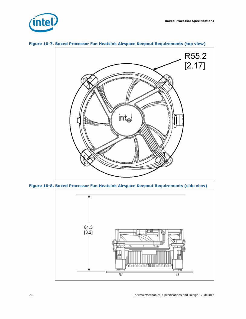
Boxed Processor Specifications
70 Thermal/Mechanical Specifications and Design Guidelines
Figure 10-7. Boxed Processor Fan Heatsink Airspace Keepout Requirements (top view)
Figure 10-8. Boxed Processor Fan Heatsink Airspace Keepout Requirements (side view)
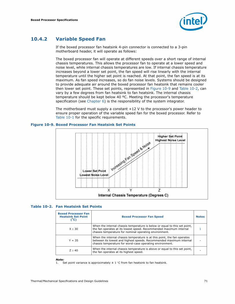
Thermal/Mechanical Specifications and Design Guidelines 71
Boxed Processor Specifications
10.4.2 Variable Speed Fan
If the boxed processor fan heatsink 4-pin connector is connected to a 3-pin motherboard header, it will operate as follows:
The boxed processor fan will operate at different speeds over a short range of internal chassis temperatures. This allows the processor fan to operate at a lower speed and noise level, while internal chassis temperatures are low. If internal chassis temperature increases beyond a lower set point, the fan speed will rise linearly with the internal temperature until the higher set point is reached. At that point, the fan speed is at its maximum. As fan speed increases, so do fan noise levels. Systems should be designed to provide adequate air around the boxed processor fan heatsink that remains cooler then lower set point. These set points, represented in Figure 10-9 and Table 10-2, can vary by a few degrees from fan heatsink to fan heatsink. The internal chassis temperature should be kept below 40 ºC. Meeting the processor's temperature specification (see Chapter 6) is the responsibility of the system integrator.
The motherboard must supply a constant +12 V to the processor's power header to ensure proper operation of the variable speed fan for the boxed processor. Refer to Table 10-1 for the specific requirements.
Note:1. Set point variance is approximately ± 1 °C from fan heatsink to fan heatsink.
Figure 10-9. Boxed Processor Fan Heatsink Set Points
Table 10-2. Fan Heatsink Set Points
Boxed Processor Fan Heatsink Set Point
(ºC)Boxed Processor Fan Speed Notes
X ≤ 30When the internal chassis temperature is below or equal to this set point, the fan operates at its lowest speed. Recommended maximum internal chassis temperature for nominal operating environment.
1
Y = 35When the internal chassis temperature is at this point, the fan operates between its lowest and highest speeds. Recommended maximum internal chassis temperature for worst-case operating environment.
-
Z ≥ 40 When the internal chassis temperature is above or equal to this set point, the fan operates at its highest speed. -
Boxed Processor Specifications
72 Thermal/Mechanical Specifications and Design Guidelines
If the boxed processor fan heatsink 4-pin connector is connected to a 4-pin motherboard header and the motherboard is designed with a fan speed controller with PWM output (CONTROL see Table 10-1) and remote thermal diode measurement capability, the boxed processor will operate as follows:
As processor power has increased the required thermal solutions have generated increasingly more noise. Intel has added an option to the boxed processor that allows system integrators to have a quieter system in the most common usage.
The 4th wire PWM solution provides better control over chassis acoustics. This is achieved by more accurate measurement of processor die temperature through the processor's Digital Thermal Sensors (DTS) and PECI. Fan RPM is modulated through the use of an ASIC located on the motherboard that sends out a PWM control signal to the 4th pin of the connector labeled as CONTROL. The fan speed is based on actual processor temperature instead of internal ambient chassis temperatures.
If the new 4-pin active fan heat sink solution is connected to an older 3-pin baseboard processor fan header, it will default back to a thermistor controlled mode, allowing compatibility with existing 3-pin baseboard designs. Under thermistor controlled mode, the fan RPM is automatically varied based on the Tinlet temperature measured by a thermistor located at the fan inlet.
§
Thermal/Mechanical Specifications and Design Guidelines 73
Component Suppliers
A Component Suppliers
Note: The part numbers listed below identifies the reference components. End-users are responsible for the verification of the Intel enabled component offerings with the supplier. These vendors and devices are listed by Intel as a convenience to Intel's general customer base, but Intel does not make any representations or warranties whatsoever regarding quality, reliability, functionality, or compatibility of these devices. Customers are responsible for thermal, mechanical, and environmental validation of these solutions. This list and/or these devices may be subject to change without notice.
Table A-1. Reference Heatsink Enabled Components
Item Intel PN AVC Delta Foxconn ITW Nidec
2009B Heatsink AssemblyRCFH7-1156 (DHA-A)
E41759-002 N/A DTC-DAA07 1A01C7T00-DHA_XA02 N/A F90T12MS1Z
7-64A01A1
Clip E36830-001 A208000389 N/A N/A N/A N/A
Fastener
Base: C33389Cap: E63768-001
N/A N/A N/A
Base: C33389Cap: E63768-001
N/A
Table A-2. LGA1156 Socket and ILM Components
Item Intel PN Foxconn Molex Tyco Lotes
LGA1156 Socket E51948-002 PE115627-4041-01F 475961132 2013092-1 N/A
LGA1156 ILM E36142-002 PT44L11-6401 475969910 2013882-3 ACA-ZIF-078-T02
Back Plate (with Screws)
E36143-002 PT44P11-6401 475969930 2069838-2 DCA-HSK-144-T01

Component Suppliers
74 Thermal/Mechanical Specifications and Design Guidelines
The enabled components may not be currently available from all suppliers. Contact the supplier directly to verify time of component availability.
§
Table A-3. Supplier Contact Information
Supplier Contact Phone Email
AVC (Asia Vital Components Co., Ltd.)
Kai Chang +86 755 3366 8888 x63588 [email protected]
Delta William Bradshaw
+1 510 668 5570+86 136 8623 1080
Foxconn Julia Jiang +1 408 919 6178 [email protected]
ITW Fastex Roger Knell +1 773 307 9035 [email protected]
Lotes Co., Ltd. Windy Wong +1 604 721 1259 [email protected]
Molex Carol Liang +86 21 504 80889 x3301 [email protected]
Nidec Karl Mattson +1 360 666 2445 [email protected]
Tyco Billy Hsieh +81 44 844 8292 [email protected]
Thermal/Mechanical Specifications and Design Guidelines 75
Mechanical Drawings
B Mechanical Drawings
Table B-1 lists the mechanical drawings included in this appendix.
Table B-1. Mechanical Drawing List
Drawing Description Figure Number
“Socket / Heatsink / ILM Keepout Zone Primary Side (Top)” Figure B-1
“Socket / Heatsink / ILM Keepout Zone Secondary Side (Bottom)” Figure B-2
“Socket / Processor / ILM Keepout Zone Primary Side (Top)” Figure B-3
“Socket / Processor / ILM Keepout Zone Secondary Side (Bottom)” Figure B-4
“Reference Design Heatsink Assembly” Figure B-5
“Reference Fastener (Sheet 1 of 4)” Figure B-6
“Reference Fastener (Sheet 2 of 4)” Figure B-7
“Reference Fastener (Sheet 3 of 4)” Figure B-8
“Reference Fastener (Sheet 4 of 4)” Figure B-9
“Reference Clip (Sheet 1 of 2)” Figure B-10
“Reference Clip (Sheet 2 of 2)” Figure B-11
“Thermocouple Attach Drawing” Figure B-12
Mechanical Drawings
76 Thermal/Mechanical Specifications and Design Guidelines
Figure B-1. Socket / Heatsink / ILM Keepout Zone Primary Side (Top)
()
95.0
(75.0
0 2
X)
(75.0
0 2
X)
(95.0
0)
(95.0
0)
(36.0
0)
4X
NP
TH
4.0
3+
0.0
5-0
.03
4X
NO
RO
UT
E6.0
0+
0.0
5-0
.03
3X
NP
TH
3.8
0+
0.0
5-0
.03
3X
N
O R
OU
TE
ON
PR
IMA
RY
& S
EC
ON
DA
RY
SID
ES
6
3 X
4.7
0 N
O R
OU
TE
ON
A
LL O
TH
ER
LA
YE
RS
6.0
0+
0.0
5-0
.03
40.71
0.00
35.21
2X 25.25
2X 21.25
10.50
5.40
20.90
26.70
25.81
37.31
45.50
23.81
40.7139.63
29.69
38.18 2X 38.12
35.21
20.13
21.25
28.46
2X 38.40
2X 36.89
37.54
18.90
10.00
10.00
NO
RO
UT
E O
N
PR
IMA
RY
SID
E
6
7.0
0
2X
37.5
0
0.0
0
2X
37.5
6 29.0
8
26.1
121.2
5
6.1
5
6.1
5
13.9
7
31.6
1
32.5
0
35.8
0
2X
37.5
0 46.4
2
47.5
0 2
X39.0
1
29.6
728.0
026.0
0
23.7
0
18.0
0
18.0
0
23.7
025.7
0
25.7
0
26.0
0
2X
29.6
730.0
0
2X
39.0
1
37.6
3
47.5
0
7.6
2
2.5
4
26.4
0
2X
39.4
9 34.4
2
40.10
35.03
27.02
25.79
33.80
48.12
46.89
()
6.0
0
E21319_R
EV
_L_P
AE
1L
DW
G.
NO
SH
T.
RE
V
DE
PA
RT
ME
NT
R2
20
0 M
ISS
ION
CO
LL
EG
E B
LV
D.
P.O
. B
OX
58
11
9S
AN
TA
CL
AR
A,
CA
95
05
2-8
11
9
TIT
LE L
GA
1156 &
1155 S
OC
KE
T A
TX
KE
EP
-IN
S
SIZ
E D
RA
WIN
G N
UM
BE
RR
EV
A1
E21319_R
EV
_L_P
AE
LS
CA
LE
: N
ON
ED
O N
OT
SC
AL
E D
RA
WIN
GS
HE
ET1
OF
2
UN
LE
SS
OT
HE
RW
ISE
SP
EC
IFIE
DIN
TE
RP
RE
T D
IME
NS
ION
S A
ND
TO
LE
RA
NC
ES
IN A
CC
OR
DA
NC
E W
ITH
AS
ME
Y1
4.5
M-1
99
4D
IME
NS
ION
S A
RE
IN
MIL
LIM
ET
ER
S
TH
IRD
AN
GL
E P
RO
JE
CT
ION
NO
TE
S:
1. D
IME
NS
ION
S A
RE
IN
MIL
LIM
ET
ER
S.
2 G
EO
ME
TR
IC C
EN
TE
R O
F S
OC
KE
T H
OU
SIN
G C
AV
ITY
.
3. B
OA
RD
CO
MP
ON
EN
ET
KE
EP
-IN
S A
ND
ME
CH
AN
ICA
L C
OM
PO
NE
NE
T K
EE
P-O
UT
S T
O B
E U
TIL
IZE
D W
ITH
SU
FF
ICIE
NT
ALLO
WA
NC
ES
FO
R P
LA
CE
ME
NT
AN
D S
IZE
TO
LE
RA
NC
ES
, A
SS
EM
BLY
PR
OC
ES
S A
CC
ES
S, A
ND
DY
NA
MIC
EX
CU
RS
ION
S.
4. A
SS
UM
E S
YM
ME
TR
Y F
OR
UN
DIM
EN
SIO
NE
D C
OR
NE
RS
AN
D E
DG
ES
.
5 R
EF
ER
TO
IN
TE
L P
AR
T D
RA
WIN
G E
21320 F
OR
ILM
AN
D S
OC
KE
T K
EE
PIN
VO
LU
ME
DIM
EN
SIO
NS
.
6 C
OP
PE
R P
AD
ON
PR
IMA
RY
SID
E, N
ON
-GR
OU
ND
ED
.
C
OP
PE
R P
AD
CA
N IN
SE
T A
MA
XIM
UM
OF
0.1
27M
M F
RO
M T
HE
NO
RO
UT
E E
DG
E.
7 C
OM
BIN
ED
CO
MP
ON
EN
T A
ND
SO
LD
ER
PA
ST
E H
EIG
HT
IN
CLU
DIN
G T
OLE
RA
NC
ES
AF
TE
R R
EF
LO
W.
BO
AR
D P
RIM
AR
Y S
IDE
2
2
WE
ST
EA
ST
SO
UT
H
NO
RT
H
PIN
1
ILM
BO
UN
DR
Y
5
LE
VE
R U
NH
OO
KE
D P
OS
ITIO
N
PA
CK
AG
E B
OU
ND
RY
SIL
KS
CR
EE
N O
UT
LIN
EO
N P
RIM
AR
Y S
IDE
AS
SH
OW
N
LE
GE
ND
SO
CK
ET
/TH
ER
MA
L/M
EC
HA
NIC
AL C
OM
PO
NE
NT
KE
EP
-IN
S
10.1
0 M
M M
AX
CO
MP
ON
EN
T H
EIG
HT
7
1.6
MM
MA
X C
OM
PO
NE
NT
HE
IGH
T
7
1.2
MM
MA
X C
OM
PO
NE
NT
HE
IGH
T
7
BO
AR
D R
OU
TIN
G K
EE
P-O
UT
27 M
M M
AX
CO
MP
ON
EN
T H
EIG
HT
7
BO
AR
D R
OU
TIN
G S
UR
FA
CE
TR
AC
E K
EE
P-O
UT
2.0
7 M
M M
AX
CO
MP
ON
EN
T H
EIG
HT
7
2.5
MM
MA
X C
OM
PO
NE
NT
HE
IGH
T
7
26 M
M M
AX
CO
MP
ON
EN
T H
EIG
HT
7
Thermal/Mechanical Specifications and Design Guidelines 77
Mechanical Drawings
Figure B-2. Socket / Heatsink / ILM Keepout Zone Secondary Side (Bottom)
(78.2
5)
(36.0
0)
(18.7
2)
37.54
0.00
25.81
13.67
35.2135.21
40.71
13.67
4X
6.0
0
4X
10.0
0
(61.0
2) 4
XR
1.8
(52.0
0)
26.0
0
0.0
0
10.8
0
7.0
5
26.0
0
18.0
0
18.0
0
9.3
6
9.3
6
(27.3
3)
DE
PA
RT
ME
NT
R2
20
0 M
ISS
ION
CO
LL
EG
E B
LV
D.
P.O
. B
OX
58
11
9S
AN
TA
CL
AR
A,
CA
95
05
2-8
11
9
SIZ
E D
RA
WIN
G N
UM
BE
RR
EV
A1
E21319_R
EV
_L_P
AE
LS
CA
LE
:1.0
00
DO
NO
T S
CA
LE
DR
AW
ING
SH
EE
T2
OF
2
BO
AR
D S
EC
ON
DA
RY
SID
E
2
2
WE
ST
EA
ST
SO
UT
H
NO
RT
H
SO
CK
ET
& P
RO
CE
SS
OR
VO
LU
ME
TR
IC K
EE
P-I
N
INT
EL P
N E
21320
CO
MP
ON
EN
T V
OLU
ME
TR
ICK
EE
PIN
S
SO
CK
ET
& P
RO
CE
SS
OR
VO
LU
ME
TR
IC K
EE
P-I
N O
UT
LIN
E
RO
UT
ING
KE
EP
OU
TS
LE
GE
ND
CO
MP
ON
EN
T K
EE
P-O
UT
RO
UT
ING
AN
D C
OM
PO
NE
NT
KE
EP
-OU
T
MA
X C
OM
PO
NE
NT
HE
IGH
T 2
.54M
M
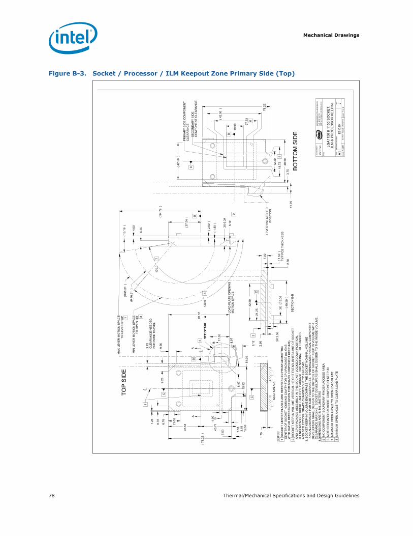
Mechanical Drawings
78 Thermal/Mechanical Specifications and Design Guidelines
Figure B-3. Socket / Processor / ILM Keepout Zone Primary Side (Top)
AA
BB
DE
PA
RT
ME
NT
R2200 M
ISS
ION
CO
LLE
GE
BLV
D.
P.O
. B
OX
58119
SA
NT
A C
LA
RA
, C
A 9
5052-8
119
PS
T-T
MI
TIT
LE
LG
A1156 &
1155 S
OC
KE
T,
ILM
& P
RO
CE
SS
OR
KE
EP
INS
IZE
DR
AW
ING
NU
MB
ER
RE
V
A1
E21320
JS
CA
LE
:1
.00
0D
O N
OT
SC
ALE
DR
AW
ING
SH
EE
T1
OF
2
51.0
0
70.3
7
17.0
0
7170.0
()
15.1
6
8.1
2
49.5
03.7
511.7
5
9.2
69.2
6
8.9
7
8.9
7
6.5
5 3X
6.3
4
6.7
6
6.7
6
1.2
5
13.0
0
5.5
040.7
1
37.5
4
()
78.2
5
CL
EA
RA
NC
E N
EE
DE
DF
OR
WIR
E T
RA
VE
L
3.7
5
4.0
0
8130.0
618.7
2
6
27.3
3
3.1
8
3.1
815.9
219.5
0
()
42.5
0
()
42.5
0
4.0
0
1.7
5
7.0
0
()
TY
P P
CB
TH
ICK
NE
SS
1.5
0
2.5
0(
)49.5
0
2.5
0
28.1
2
42.5
0
21.2
5
()
94.7
6
78.2
5
3X
2.5
83X
5.0
0
12.2
9
19.9
9
B
C
C
B
B
C
C
(R)
65.2
1
(R)
46.5
1
()
37.5
4
()
2.5
0
()
1.5
0
NO
TE
S:
1 S
OC
KE
T C
EN
TE
R P
LA
NE
S A
RE
RE
FE
RE
NC
ED
FR
OM
GE
OM
ET
RIC
C
EN
TE
R O
F S
OC
KE
T H
OU
SIN
G C
AV
ITY
FO
R C
PU
PA
CK
AG
E (
ALIG
NS
W
ITH
DA
TU
M R
EF
ER
EN
CE
GIV
EN
FO
R B
OA
RD
CO
MP
ON
EN
T K
EE
P-I
NS
).
2 S
OC
KE
T K
EE
P-I
N V
OLU
ME
VE
RT
ICA
L H
EIG
HT
ES
TA
BLIS
HE
S L
IMIT
OF
SO
CK
ET
A
ND
CP
U P
AC
KA
GE
AS
SE
MB
LY
IN
TH
E S
OC
KE
T L
OC
KE
D D
OW
N P
OS
ITIO
N.
IT
EN
CO
MP
AS
SE
S S
OC
KE
T A
ND
CP
U P
AC
KA
GE
DIM
EN
SIO
NA
L T
OLE
RA
NC
ES
A
ND
DE
FLE
CT
ION
/ S
HA
PE
CH
AN
GE
S D
UE
TO
ILM
LO
AD
. 3. S
OC
KE
T K
EE
P-I
N V
OLU
ME
EN
CO
MP
AS
S T
HE
SO
CK
ET
NO
MIN
AL V
OLU
ME
A
ND
ALLO
WA
NC
ES
FO
R S
IZE
TO
LE
RA
NC
ES
. T
HE
RM
AL/M
EC
HA
NIC
AL C
OM
PO
NE
NT
D
EV
ELO
PE
RS
SH
ALL D
ES
IGN
TO
TH
E O
UT
SID
E O
F S
OC
KE
T K
EE
P IN
VO
LU
ME
WIT
H C
LE
AR
AN
CE
MA
RG
INS
. S
OC
KE
T D
EV
ELO
PE
RS
SH
ALL D
ES
IGN
TO
TH
E IN
SID
E V
OLU
ME
.4.D
IME
NS
ION
S A
RE
IN
MIL
LIM
ET
ER
S
5 N
O C
OM
PO
NE
NT
BO
UN
DA
RY
-FIN
GE
R A
CC
ES
S A
RE
A
6 M
OT
HE
RB
OA
RD
BA
CK
SID
E C
OM
PO
NE
NT
KE
EP
-IN
7 M
AX
IMU
M O
PE
N A
NG
LE
TO
OP
EN
LO
AD
PLA
TE
8 M
INIM
UM
OP
EN
AN
GLE
TO
CLE
AR
LO
AD
PLA
TE
TO
P S
IDE
BO
TT
OM
SID
E
1
2
SE
CT
ION
A-A
SE
CT
ION
B-B
SE
E D
ET
AIL
A
5
MA
X L
EV
ER
MO
TIO
N S
PA
CE
TO
LE
VE
R S
TO
P 7
LO
AD
PLA
TE
OP
EN
ING
M
OT
ION
SP
AC
E
MIN
LE
VE
R M
OT
ION
SP
AC
ET
O O
PE
N L
ID 8
PR
IMA
RY
SID
E C
OM
PO
NE
NT
CLE
AR
AN
CE
LE
VE
R U
NLA
TC
HE
DP
OS
ITIO
N
SE
CO
ND
AR
Y S
IDE
C
OM
PO
NE
NT
CLE
AR
AN
CE
SE
E D
ET
AIL
A
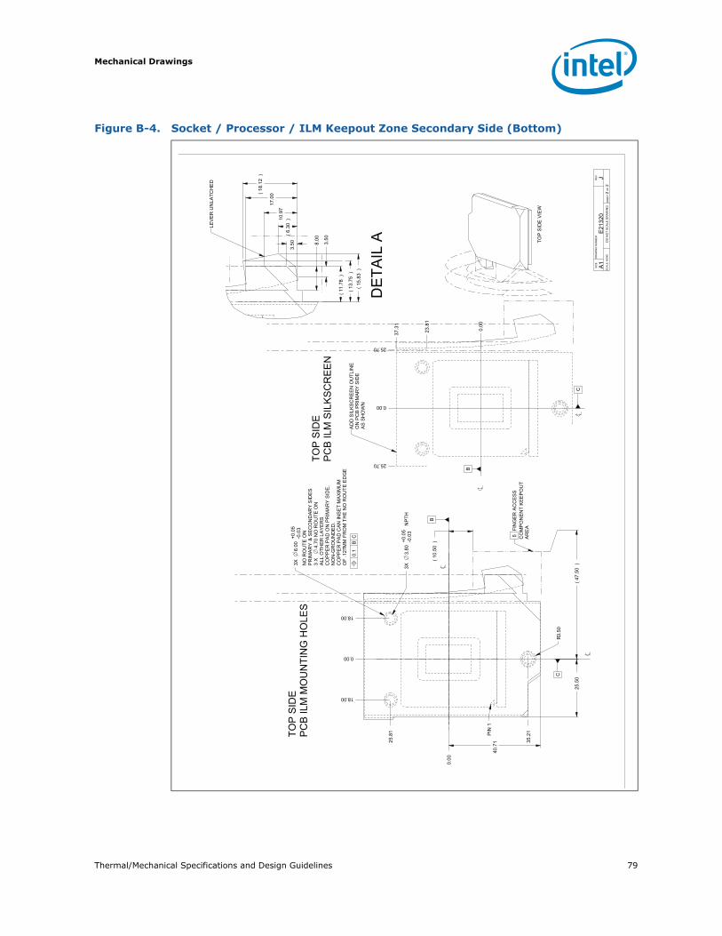
Thermal/Mechanical Specifications and Design Guidelines 79
Mechanical Drawings
Figure B-4. Socket / Processor / ILM Keepout Zone Secondary Side (Bottom)
SIZ
E D
RA
WIN
G N
UM
BE
RR
EV
A1
E21320
JS
CA
LE
: N
ON
ED
O N
OT
SC
ALE
DR
AW
ING
SH
EE
T2
OF
2
0.1
BC
25.8
1
18.00
0.00
0.0
0
18.00
3X
NO
RO
UT
E O
N
PR
IMA
RY
& S
EC
ON
DA
RY
SID
ES
3 X
4.7
0 N
O R
OU
TE
ON
A
LL O
TH
ER
LA
YE
RS
CO
PP
ER
PA
D O
N P
RIM
AR
Y S
IDE
, N
ON
-GR
OU
ND
ED
.C
OP
PE
R P
AD
CA
N I
NS
ET
MA
XIM
UM
O
F .
12
7M
M F
RO
M T
HE
NO
RO
UT
E E
DG
E
6.0
0+
0.0
5-0
.03
3X
NP
TH
3.8
0+
0.0
5-0
.03
()
11.7
8
8.0
0
3.5
0
17.0
0()
18.1
2
10.9
7
3.5
0(
)6.3
0
35.2
1
25.5
0
40.7
1
25.70
0.00
25.70
23.8
1
0.0
0
37.3
1
R3.5
0
B
C
B
C
()
15.8
3
()
13.7
5
()
10.5
0
()
47.5
0
TO
P S
IDE
VIE
W
TO
P S
IDE
PC
B ILM
MO
UN
TIN
G H
OLE
S
TO
P S
IDE
PC
B ILM
SIL
KS
CR
EE
N
DE
TA
IL A
5 F
ING
ER
AC
CE
SS
CO
MP
ON
EN
T K
EE
PO
UT
AR
EA
PIN
1
LE
VE
R U
NLA
TC
HE
D
AD
D S
ILK
SC
RE
EN
OU
TLIN
E
ON
PC
B P
RIM
AR
Y S
IDE
A
S S
HO
WN
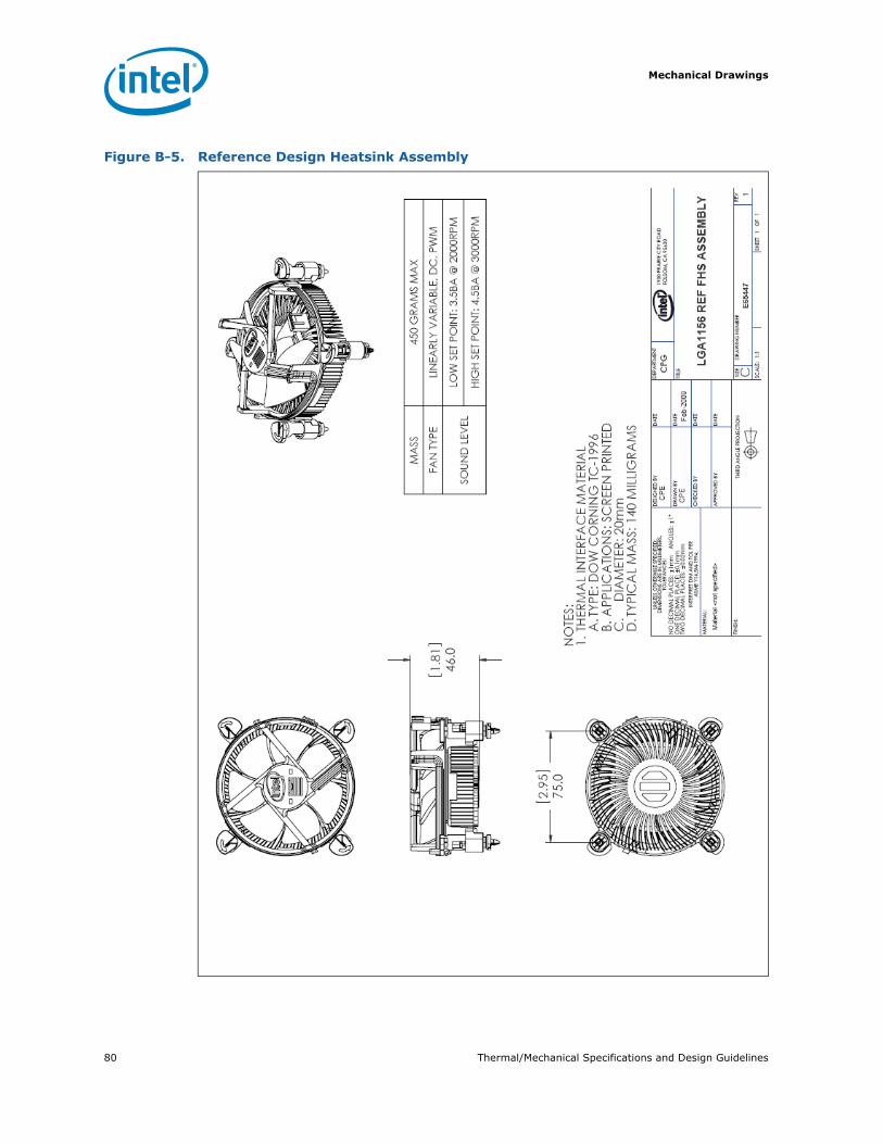
Mechanical Drawings
80 Thermal/Mechanical Specifications and Design Guidelines
Figure B-5. Reference Design Heatsink Assembly
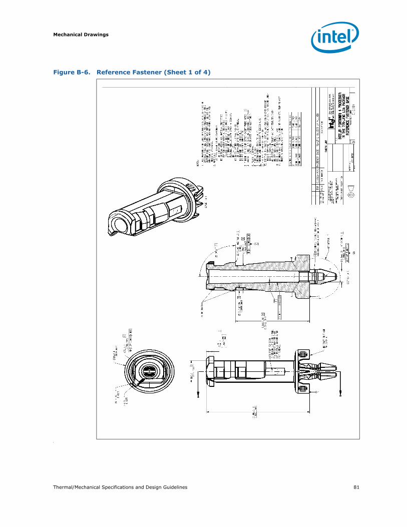
Thermal/Mechanical Specifications and Design Guidelines 81
Mechanical Drawings
(
Figure B-6. Reference Fastener (Sheet 1 of 4)
Mechanical Drawings
82 Thermal/Mechanical Specifications and Design Guidelines
Figure B-7. Reference Fastener (Sheet 2 of 4)
Thermal/Mechanical Specifications and Design Guidelines 83
Mechanical Drawings
(
Figure B-8. Reference Fastener (Sheet 3 of 4)
Mechanical Drawings
84 Thermal/Mechanical Specifications and Design Guidelines
Figure B-9. Reference Fastener (Sheet 4 of 4)
Thermal/Mechanical Specifications and Design Guidelines 85
Mechanical Drawings
Figure B-10. Reference Clip (Sheet 1 of 2)
13
45
67
8
BCD A
12
34
56
78
BCD A
AA
SH
EE
T1
OF
2D
O N
OT
SC
ALE
DR
AW
ING
SC
ALE
:3:1
01
E36830
DR
EV
DR
AW
ING
NU
MB
ER
CA
GE
CO
DE
SIZ
E
HA
VE
ND
ALE
PO
WE
R O
N S
AM
PLE
HE
AT
SIN
K C
LIP
TIT
LE
2200 M
ISS
ION
CO
LLE
GE
BLV
D.
P.O
. B
OX
58119
SA
NT
A C
LA
RA
, C
A 9
5052-8
119
CO
RP
.
R
PS
T
DE
PA
RT
ME
NT
SE
E N
OT
ES
FIN
ISH
:
SE
E N
OT
ES
MA
TE
RIA
L:
--
DA
TE
AP
PR
OV
ED
BY
--
DA
TE
CH
EC
KE
D B
Y
02/0
4/0
8K
G T
AN
DA
TE
DR
AW
N B
Y
04/0
2/0
3R
. A
OK
I
DA
TE
DE
SIG
NE
D B
Y U
NLE
SS
OT
HE
RW
ISE
SP
EC
IFIE
D:
D
IME
NS
ION
S A
RE
IN
MIL
LIM
ET
ER
S.
TO
LE
RA
NC
ES
: LIN
EA
R
.15
AN
GLE
S:
1
IN
TE
RP
RE
T D
IME
NS
ION
S A
ND
TO
LE
RA
NC
ES
P
ER
AN
SI Y
14.5
M-1
994
TH
IRD
AN
GLE
PR
OJE
CT
ION
RE
VIS
ION
HIS
TO
RY
ZO
NE
RE
VD
ES
CR
IPT
ION
DA
TE
AP
PR
OV
ED
AR
ELE
AS
E F
OR
PR
OT
OT
YP
ING
02/0
4/0
8N
A
E36830
1A
DW
G. N
OS
HT
.R
EV
PA
RT
S L
IST
DE
SC
RIP
TIO
NP
AR
T N
UM
BE
RIT
EM
NO
QT
Y P
ER
AS
SY
-001
-002
-003
CLIP
, S
TE
EL, S
TA
MP
ED
E36830-0
01
TO
P
74
.22
0.2
.16
6.0
07
[]
98
.83
.89
0[
]
98
.83
.89
0[
]
20
.2.0
79
.00
7[
]
SQ
53
.50
.22
.10
6.0
07
[]
4X
10
0.2
.39
4.0
07
[]
41
.73
1.6
43
[]
B
73
3.8
60
.21
.33
3.0
07
[]
A
()
1.6
0.0
63
[]
NO
TE
S:
1.
TH
IS D
RA
WIN
G T
O B
E U
SE
D I
N C
ON
JU
NT
ION
WIT
H S
UP
PL
IED
3D
D
AT
AB
AS
E F
ILE
. A
LL
DIM
EN
SIO
NS
AN
D T
OL
ER
AN
CE
S O
N T
HIS
D
RA
WIN
G T
AK
E P
RE
CE
DE
NC
E O
VE
R S
UP
PL
IED
FIL
E A
ND
AR
E
A
PP
LIC
AB
LE
AT
PA
RT
FR
EE
, U
NC
ON
ST
RA
INE
D S
TA
TE
UN
LE
SS
I
ND
ICA
TE
D O
TH
ER
WIS
E.
2.
MA
TE
RIA
L:
A
) T
YP
E:
AIS
I 1
06
5 C
OL
D D
RA
WN
ST
EE
L O
R E
QU
IVA
LE
NT
1
.6M
M T
HIC
KN
ES
S
.02
[.0
63
"] B
) C
RIT
ICA
L M
EC
HA
NIC
AL
MA
TE
RIA
L P
RO
PE
RT
IES
F
OR
EQ
UIV
AL
EN
T M
AT
ER
IAL
SE
LE
CT
ION
: E
LA
ST
IC M
OD
UL
US
> 2
06
.8 G
PA
[2
9,9
00
KS
I] M
IN T
EN
SIL
E Y
IEL
D S
TR
EN
GT
H (
AS
TM
D6
38
) >
3
80
MP
a [
55
KS
I] C
) M
AS
S -
37
.7 G
RA
MS
(R
EF
)3
. S
EC
ON
DA
RY
OP
ER
AT
ION
S:
A
) F
INIS
H:
NIC
KE
L P
LA
TE
RE
QU
IRE
D A
FT
ER
FO
RM
ING
4.
AL
L D
IME
NS
ION
S A
ND
TO
LE
RA
NC
ES
AR
E S
HO
WN
AF
TE
R P
LA
TIN
G
5 P
UN
CH
DIR
EC
TIO
N
6.
BR
EA
K A
LL
SH
AR
P C
OR
NE
RS
AN
D B
UR
RS
7 C
RIT
ICA
L T
O F
UN
CT
ION
DIM
EN
SIO
N
8 C
OIN
ING
RE
QU
IRE
D A
S S
PE
CIF
IED
9.
SE
CO
ND
AR
Y U
NIT
TO
LE
RA
NC
ES
SH
OU
LD
BE
CA
LC
UL
AT
ED
FR
OM
PR
IMA
RY
U
NIT
S T
O A
VO
ID R
OU
ND
OF
F E
RR
OR
.
7
0.5
[.0
1]
AB
7
0.5
[.0
1]
AB
SE
E D
ET
AIL
A
RE
MO
VE
AL
L B
UR
RS
OR
SH
AR
P E
DG
ES
AR
OU
ND
PE
RIM
ET
ER
OF
PA
RT
.S
HA
RP
NE
SS
OF
ED
GE
S S
UB
JE
CT
TO
HA
ND
LIN
G A
RE
RE
QU
IRE
D T
O
ME
ET
TH
E U
L1
43
9 T
ES
T.
PE
RM
AN
EN
TL
Y M
AR
K P
AR
TN
UM
BE
R A
ND
RE
VIS
ION
LE
VE
L
AP
PR
OX
IMA
TE
LY
WH
ER
E S
HO
WN
XX
XX
XX
-XX
X R
EV
XX
SE
CT
ION
A-A
SE
E D
ET
AIL
B
SE
E D
ET
AIL
C
SE
E D
ET
AIL
D
SE
E D
ET
AIL
A
SE
E D
ET
AIL
B
SE
E D
ET
AIL
C
SE
E D
ET
AIL
D

Mechanical Drawings
86 Thermal/Mechanical Specifications and Design Guidelines
Figure B-11. Reference Clip (Sheet 2 of 2)
13
45
67
8
12
34
56
78
SH
EE
T2
OF
2D
O N
OT
SC
ALE
DR
AW
ING
SC
ALE
:3:1
2200 M
ISS
ION
CO
LLE
GE
BLV
D.
P.O
. B
OX
58119
SA
NT
A C
LA
RA
, C
A 9
5052-8
119
CO
RP
.
R
TM
D01
E36830
DR
EV
DR
AW
ING
NU
MB
ER
SIZ
ED
EP
AR
TM
EN
T
E36830
201
DW
G. N
OS
HT
.R
EV
R T
YP
0.3 .0
11
8[
]
7.3
4.2
89
[]
R1
.4 .05
5[
]
R3
.1 .12
2[
]
43.1
3.5
7.1
41
[]
5.3 .2
08
7[
]7
.35
.28
94
[]
2X
R3
.6 .14
17
[]
1.6
5.0
65
[]
13
5
1.0
6.0
42
[]
2X
R0
.5 .01
97
[]
R M
IN0
.45
.01
77
[]
AA
DE
TA
ILA
SC
AL
E1
0:1
TY
PIC
AL
4 P
LA
CE
S
0.1
[.0
03
]A
B
0.2
[.0
07
]A
B
DE
TA
ILB
SC
AL
E1
0:1
DE
TA
ILC
SC
AL
E1
0:1
TY
P 4
PL
AC
ES
45
X 0
.25
0.0
58
[.0
10
.001]
W
X0.4
[.0
1]
AB
0.5
[.0
1]
AB
DE
TA
ILD
SC
AL
E1
0:1
TH
IS P
OIN
T C
OR
RE
SP
ON
DE
S T
O T
HE
41
.73
DIM
EN
SIO
N O
N S
HE
ET
1 Z
ON
E A
7
WX
4X
7
BO
UN
DA
RY
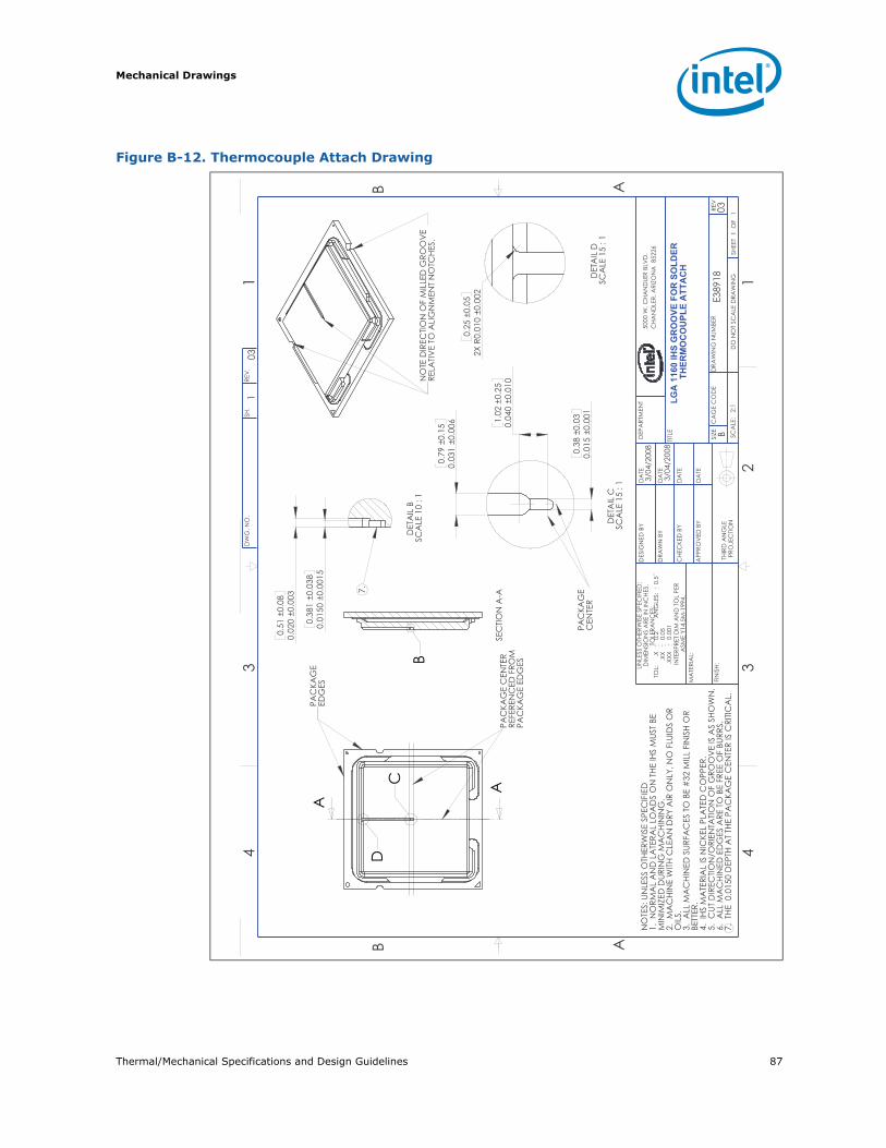
Thermal/Mechanical Specifications and Design Guidelines 87
Mechanical Drawings
Figure B-12. Thermocouple Attach Drawing

Mechanical Drawings
88 Thermal/Mechanical Specifications and Design Guidelines
§
Thermal/Mechanical Specifications and Design Guidelines 89
Socket Mechanical Drawings
C Socket Mechanical Drawings
Table C-1 lists the mechanical drawings included in this appendix.
Table C-1. Mechanical Drawing List
Drawing Description Figure Number
“Socket Mechanical Drawing (Sheet 1 of 4)” Figure C-1
“Socket Mechanical Drawing (Sheet 2 of 4)” Figure C-2
“Socket Mechanical Drawing (Sheet 3 of 4)” Figure C-3
“Socket Mechanical Drawing (Sheet 4 of 4)” Figure C-4
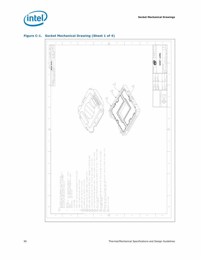
Socket Mechanical Drawings
90 Thermal/Mechanical Specifications and Design Guidelines
Figure C-1. Socket Mechanical Drawing (Sheet 1 of 4)
8 7 6 5
4 3 2
H G F E D C B A
8 7 6 5
4 3 2 1
H G F E D C B A
THIS DRAWING CONTAINS INTEL CORPORATION CONFIDENTIAL INFORMATION. IT IS DISCLOSED IN CONFIDENCE AND ITS CONTENTS
MAY NOT BE DISCLOSED, REPRODUCED, DISPLAYED OR MODIFIED, WITHOUT THE PRIOR WRITTEN CONSENT OF INTEL CORPORATION.
NOTES:
1. THE PURPOSE OF THIS DRAWING IS TO ESTABLISH THE
MECHANICAL FORM FACTOR OF THE SOCKET. THIS DRAWING IS
NOT INTENDED TO SHOW INTERNAL DETAIL OF THE SOCKET
WHICH MAY VARY FROM SUPPLIER TO SUPPLIER.
2. MATERIAL:
BASE AND CAP: HIGH TEMPERATURE THERMOPLASTIC. UL94V-0
CONTACT: HIGH STRENGTH COPPER ALLOY
POSTS: HIGH TEMPERATURE THERMOPLASTIC UL94V-0
SOLDER BALL: LEAD FREE SAC
3. FINISH: NONE
4. CONTACT MUST REMAIN ON LAND THROUGHOUT ACTUATION STROKE.
5. REMOVE ALL BURRS AND SHARP EDGES R0.05 MAX.
6 SOCKET NAME TO BE INDICATED IN THIS AREA.
7 LOT NUMBER SHALL BE INDICATED IN THIS AREA.
8 CHAMFER INDICATES THE CORNER CLOSEST TO PACKAGE PIN A1
9 CONTACT MUST REMAIN OUTSIDE THE CENTRAL CAVITY THROUGHOUT THE ACTUATION
STROKE.
10 PICK-AND-PLACE TOOLING KEEP-IN ZONE. NO THOUGH HOLES ALLOWED IN THIS ZONE.
11 SOCKET MANUFACTURER NAME SHOWN ON SIDEWALL. OPPOSITE SIDEWALL CAN BE USED
IF NEEDED.
12 ONLY THE LGA CONTACTS/SOLDER BALLS ALONG THE BOUNDARIES OF THE TWO "L"
ARRAYS ARE SHOWN
IN THE DRAWINGS.
13 THE DIMENSION MEASURED FROM THE TOP OF THE ILM KEY-IN FEATURE TO THE TOP OF
THE SOCKET
ALIGNMENT FEATURE.
14 DO NOT TOOL THIS KEY-IN FEATURE. MOLD TOOLING SHALL ALLOW THIS FEATURE TO
BE ADDED IN THE
FUTURE NO LARGER THAN THE AREA SPECIFIED.
15 SOCKET SEAT PLANES.
REVISION HISTORY
ZONE
REV
DESCRIPTION
DATE
APPROVED
-1
PRELIMINARY RELEASE
10/23/07
-
E27147
14
DWG. NO
SHT.
REV
DEPARTMENT
R2200 MISSION COLLEGE BLVD.
P.O. BOX 58119
SANTA CLARA, CA 95052-8119
-
TITLE
SOCKET LGA1156
SIZE
DRAWING NUMBER
REV
A1
E27147
4SCALE:4
DO NOT SCALE DRAWING
SHEET1 OF 4
SEE NOTES
SEE NOTES
FINISH
MATERIAL
--
DATE
APPROVED BY
--
--
DATE
CHECKED BY
02/28/07
B. KNAPIK
DATE
DRAWN BY
02/28/07
L. YUPENG
DATE
DESIGNED BY
THIRD ANGLE PROJECTION
6
7
11
12
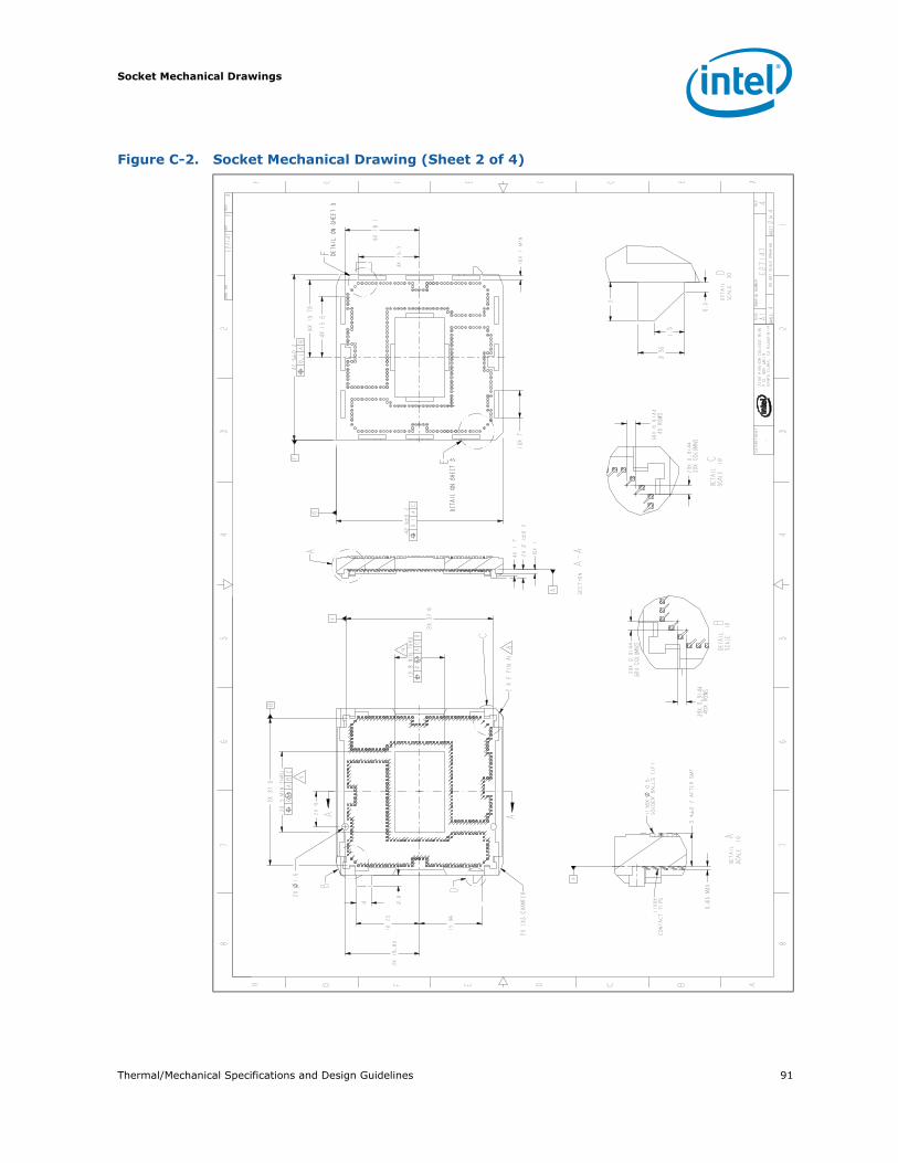
Thermal/Mechanical Specifications and Design Guidelines 91
Socket Mechanical Drawings
Figure C-2. Socket Mechanical Drawing (Sheet 2 of 4)
H G F E D C B A
H G F E D C B A
8 7 6 5
4 3 2
8 7 6 5
4 3 2 1
AA
A
A
0.1
AB
42.5
#0.2
20.5 MIN THRU
0A
BC
12.8 MIN THRU
0A
CB
0.1
AC
42.5
#0.2
B2X
37.6
C
2X
37.6
4X
1.7
2X
2.1
#0.2
3.4
#0.2 AFTER SMT
0.65 MAX
29X
0.9144
30X COLUMNS
39X
0.9144
40X ROWS
39X
0.9144
40 ROWS
16X
1 MIN
16X
7
2X
18.95
29X
0.9144
30X COLUMNS
2X
9
2X
1.6
6X
1
6X
19.75
4X
15.5
6X
19.1
4X
15.5
4 2.9
2
1.5
2.35
15.96
0.5
16.25
F
G
THIS DRAWING CONTAINS INTEL CORPORATION CONFIDENTIAL INFORMATION. IT IS DISCLOSED IN CONFIDENCE AND ITS CONTENTS
MAY NOT BE DISCLOSED, REPRODUCED, DISPLAYED OR MODIFIED, WITHOUT THE PRIOR WRITTEN CONSENT OF INTEL CORPORATION.
E27147
24
DWG. NO
SHT.
REV
DEPARTMENT
R2200 MISSION COLLEGE BLVD.
P.O. BOX 58119
SANTA CLARA, CA 95052-8119
-
SIZE
DRAWING NUMBER
REV
A1
E27147
4SCALE:4
DO NOT SCALE DRAWING
SHEET2 OF 4
B
C
2 X 2 PIN A1
2X 1X3 CHAMFER
D
SECTIONA-AA
EDETAIL ON SHEET 3
F DETAIL ON SHEET 3
DETAILA
SCALE
10
1156X
0.6
SOLDER BALLS (LF)
1156X
CONTACT TIPS
DETAILB
SCALE
10
DETAILC
SCALE
10
DETAILD
SCALE
20
EDETAIL ON SHEET 3
F DETAIL ON SHEET 3
89
9
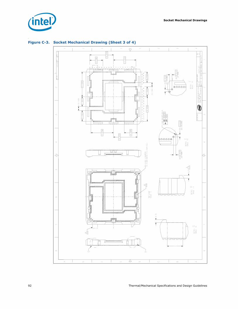
Socket Mechanical Drawings
92 Thermal/Mechanical Specifications and Design Guidelines
(
Figure C-3. Socket Mechanical Drawing (Sheet 3 of 4)
H G F E D C B A
H G F E D C B A
8 7 6 5
4 3 2
8 7 6 5
4 3 2 1
39X
0.9144
40X ROWS
29X
0.9144
30X COLUMNS
39X
0.9144
40 ROWS
29X
0.9144
30X COLUMNS
0.75
17.3738
7.5868
8.2296
(3.1144)
18.9308
10.0584 18.2878
17.3738
8.2296
(3.1144)
7.5868
18.9308
18.2878 10.0584
0.75
4
THIS DRAWING CONTAINS INTEL CORPORATION CONFIDENTIAL INFORMATION. IT IS DISCLOSED IN CONFIDENCE AND ITS CONTENTS
MAY NOT BE DISCLOSED, REPRODUCED, DISPLAYED OR MODIFIED, WITHOUT THE PRIOR WRITTEN CONSENT OF INTEL CORPORATION.
E27147
34
DWG. NO
SHT.
REV
DEPARTMENT
R2200 MISSION COLLEGE BLVD.
P.O. BOX 58119
SANTA CLARA, CA 95052-8119
-
SIZE
DRAWING NUMBER
REV
A1
E27147
4SCALE:6
DO NOT SCALE DRAWING
SHEET3 OF 4
DETAILE
SCALE
10
1156X SOLDER BALLS
DETAILF
SCALE
10
AY
AW
AV
AU
AT
AR
AP
AN
AM
AL
AK
AJ
AH
AG
AF
AE
AD
AC
AB
AA
Y
W
V
U
T
R
P
N
M
L
K
J
H
G
F
E
D
C
B
A
1 3 5 7 9 11 13 15 17 19 21 23 25 27 29
2 4 6 8 10 12 14 16 18 20 22 24 26 28 3031 33 35 37 39
32 34 36 38 40
0.3
AFG
0.25
A
TOP VIEW
SCALE
5
8X 0.4X0.5 CHAMFER
(0.4 HORIZONTAL 0.5 VERTICAL)
14
15
HG
DETAILH
SCALE
15
DETAILG
SCALE
15
13
0.3
AFG
0.25
A
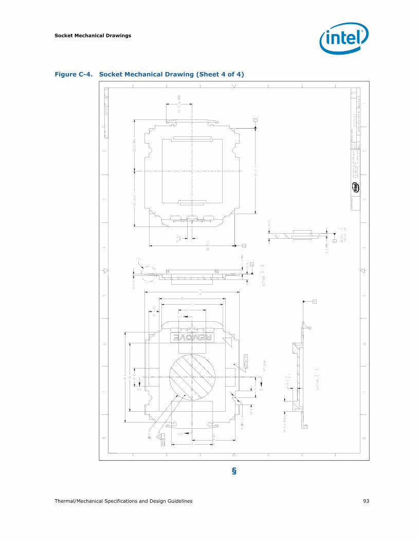
Thermal/Mechanical Specifications and Design Guidelines 93
Socket Mechanical Drawings
§
Figure C-4. Socket Mechanical Drawing (Sheet 4 of 4)
H G F E D C B A
8 7 6 5
4 3 2
8 7 6 5
4 3 2 1
AA
EE
H
K
J
H
H
39.6
30
2X
4.45
27
41.5
29
2X
6
2X
18.95
2X
9
2X
2.5
2.41.9 MAX
2X
0.6
22.55 MAX
2X
11.35 MAX
2X
37.5
2X
37.52X
2.1
MAX
0.3 MAX
(0.6)
2X
8
20
18
12
2X
4.5 MAX
2X
2 0-0.1
24.56
#0.1
THIS DRAWING CONTAINS INTEL CORPORATION CONFIDENTIAL INFORMATION. IT IS DISCLOSED IN CONFIDENCE AND ITS CONTENTS
MAY NOT BE DISCLOSED, REPRODUCED, DISPLAYED OR MODIFIED, WITHOUT THE PRIOR WRITTEN CONSENT OF INTEL CORPORATION.
E27147
44
DWG. NO
SHT.
REV
DEPARTMENT
R2200 MISSION COLLEGE BLVD.
P.O. BOX 58119
SANTA CLARA, CA 95052-8119
-
SIZE
DRAWING NUMBER
REV
A1
E27147
4SCALE:5
DO NOT SCALE DRAWING
SHEET4 OF 4
TOP VIEW
10
0.35
J
SECTIONA-A
SECTIONE-E
DETAILJ
SCALE
20
0.1

Socket Mechanical Drawings
94 Thermal/Mechanical Specifications and Design Guidelines
Thermal/Mechanical Specifications and Design Guidelines 95
Package Mechanical Drawings
D Package Mechanical Drawings
Table D-1 lists the mechanical drawings included in this appendix.
Table D-1. Mechanical Drawing List
Drawing Description Figure Number
“Processor Package Drawing (Sheet 1 of 2)” Figure D-1
“Processor Package Drawing (Sheet 2 of 2)” Figure D-2
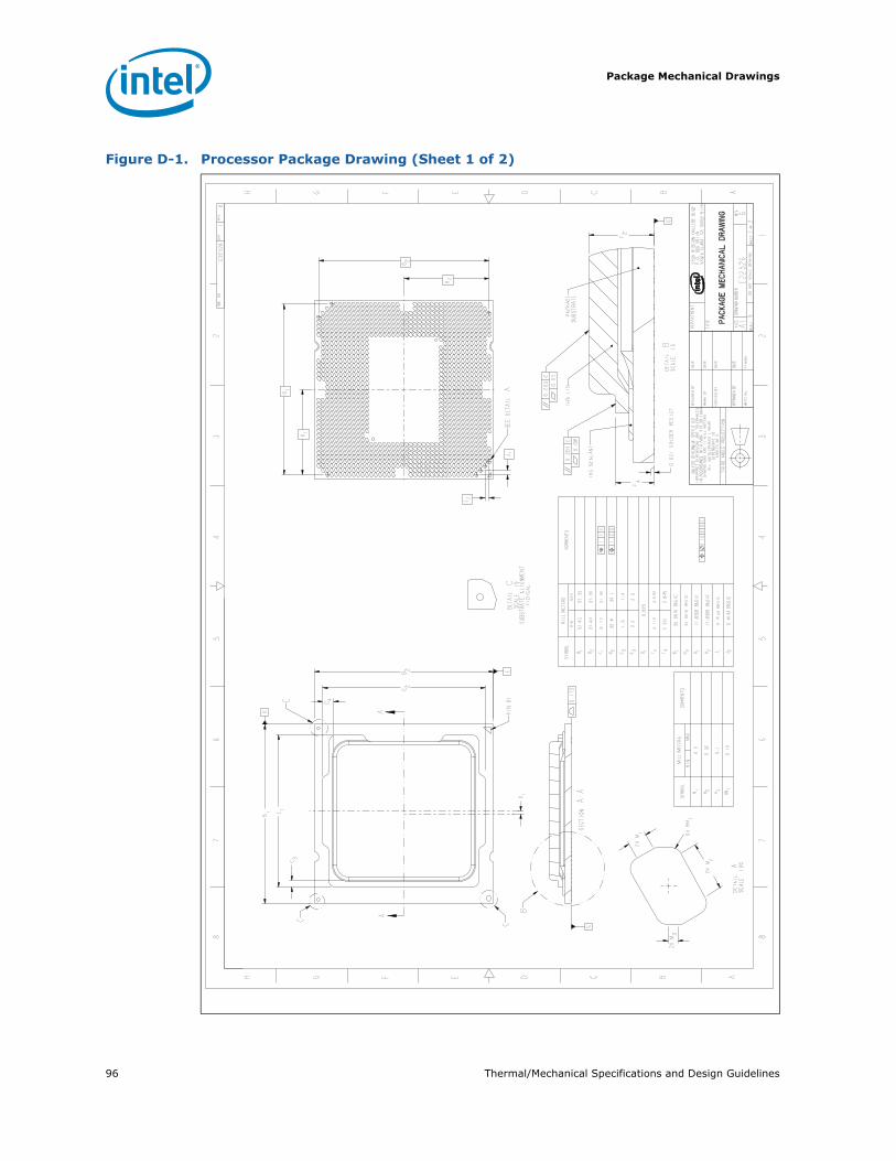
Package Mechanical Drawings
96 Thermal/Mechanical Specifications and Design Guidelines
Figure D-1. Processor Package Drawing (Sheet 1 of 2)
8 7 6 5
4 3 2
H G F E D C B A
8 7 6 5
4 3 2 1
H G F E D C B A
AA
E
D
C
C
B2
B1 C1
C2
J2
H2
J1
6X RM1
2X
M1
2X
M2
2X
M3
F2
F4
D1
G1
H1
G2
C4
C3
0.021 SOLDER RESIST
THIS DRAWING CONTAINS INTEL CORPORATION CONFIDENTIAL INFORMATION. IT IS DISCLOSED IN CONFIDENCE AND ITS CONTENTS
MAY NOT BE DISCLOSED, REPRODUCED, DISPLAYED OR MODIFIED, WITHOUT THE PRIOR WRITTEN CONSENT OF INTEL CORPORATION.
E22526
16
DWG. NO
SHT.
REV
DEPARTMENT
R2200 MISSION COLLEGE BLVD.
P.O. BOX 58119
SANTA CLARA, CA 95052-8119
TITLE PACKAGE MECHANICAL DRAWING
SIZE
DRAWING NUMBER
REV
A1
E22526
6SCALE:5
DO NOT SCALE DRAWING
SHEET1 OF 2
FINISH
MATERIAL
DATE
APPROVED BY
DATE
CHECKED BY
DATE
DRAWN BY
DATE
DESIGNED BY
UNLESS OTHERWISE SPECIFIED
INTERPRET DIMENSIONS AND TOLERANCES
IN ACCORDANCE WITH ASME Y14.5M-1994
DIMENSIONS ARE IN MILLIMETERS
ALL UNTOLERANCED LINEAR
DIMENSIONS ±0
ANGLES ±0.5
THIRD ANGLE PROJECTION
C
C
C
PIN #1
SEE DETAIL
A
B
SECTION
A-A
DETAIL
ASCALE
100
DETAIL
BSCALE
15
IHS SEALANT
0.203
C
0.08
0.203
C
0.05
IHS LID
PACKAGE
SUBSTRATE
DETAIL
CSCALE
15
SUBSTRATE ALIGNMENT
FIDICAL
SYMBOL
MILLIMETERS
COMMENTS
MIN
MAX
B1
37.45
37.55
B2
37.45
37.55
C1
31.72
31.92
1C
E
C2
33.9
34.1
1C
D
C3
1.3
1.4
C4
2.2
2.3
D1
0.625
F2
4.112
4.602
F4
2.331
2.843
G1
35.6616 BASIC
0.15
CD
E
G2
35.6616 BASIC
H1
17.8308 BASIC
H2
17.8308 BASIC
J1
0.9144 BASIC
J2
0.9144 BASIC
SYMBOL
MILLIMETERS
COMMENTS
MIN
MAX
M1
0.2
M2
0.52
M3
0.1
RM1
0.13
0.175
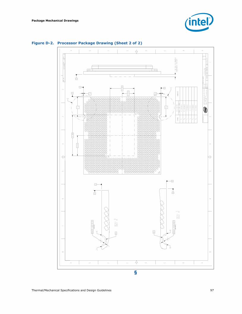
Thermal/Mechanical Specifications and Design Guidelines 97
Package Mechanical Drawings
§
Figure D-2. Processor Package Drawing (Sheet 2 of 2).
H G F E D C B A
H G F E D C B A
8 7 6 5
4 3 2
8 7 6 5
4 3 2 1
H
GF
HF
HG
CT1
T2
V1
V2
19.68
11.95
9.84
5.975
R1 R2
1.06 MAX ALLOWABLE
COMPONENT HEIGHT
THIS DRAWING CONTAINS INTEL CORPORATION CONFIDENTIAL INFORMATION. IT IS DISCLOSED IN CONFIDENCE AND ITS CONTENTS
MAY NOT BE DISCLOSED, REPRODUCED, DISPLAYED OR MODIFIED, WITHOUT THE PRIOR WRITTEN CONSENT OF INTEL CORPORATION.
E22526
26
DWG. NO
SHT.
REV
DEPARTMENT
R2200 MISSION COLLEGE BLVD.
P.O. BOX 58119
SANTA CLARA, CA 95052-8119
SIZE
DRAWING NUMBER
REV
A1
E22526
6SCALE:6
DO NOT SCALE DRAWING
SHEET2 OF 2
D
E
0.23
CF
HJ
K
JK
DETAIL
DSCALE
20
0.23
CG
HM
N
NM
DETAIL
ESCALE
20
SYMBOL
MILLIMETERS
COMMENTS
MIN
MAX
R1
R1.09 BASIC
R2
R1.09 BASIC
T1
9.75 BASIC
T2
0.2 BASIC
V1
9.75 BASIC
V2
0.2 BASIC

Package Mechanical Drawings
98 Thermal/Mechanical Specifications and Design Guidelines
Thermal/Mechanical Specifications and Design Guidelines 99
Heat Sink Back Plate Drawings
E Heat Sink Back Plate Drawings
This heat sink back plate design is intended to adapt as a reference for OEMs that use threaded fasteners on customized thermal solution, to comply with the mechanical and structural requirements for the LGA1156 socket. The heat sink back plate does not have to provide additional load for socket solder joint protect. Structural design strategy for the heat sink is to provide sufficient load for the Thermal Interface Material (TIM) and to minimize stiffness impact on the motherboard.
Note: Design modifications for specific application and manufacturing are the responsibility of OEM and the listed vendors for customized system implementation and validation. These vendors and devices are listed by Intel as a convenience to Intel's general customer base, but Intel does not make any representations or warranties whatsoever regarding quality, reliability, functionality, or compatibility of these devices. Customers are responsible for thermal, mechanical, and environmental validation of these solutions. This list and/or these devices may be subject to change without notice.
Please refer to the motherboard keep out zone listed in Appendix B to ensure compliant with the heat sink back plate implementation. Figure E-1 is the heat sink back plate keep in zone for the design implementation.
Table E-1 lists the mechanical drawings included in this appendix. Table E-2 lists the mechanical drawings.
The enabled components may not be currently available from supplier. Contact the supplier directly to verify time of component availability.
Table E-1. Mechanical Drawing List
Drawing Description Figure Number
“Heat Sink Back Plate Keep In Zone” Figure E-1
“Heat Sink Back Plate” Figure E-2
Table E-2. Supplier Contact Information
Supplier Contact Phone Email
CCI (Chaun Choung Technology Corp.)
Monica Chih +886-2-29952666 x1131 [email protected]
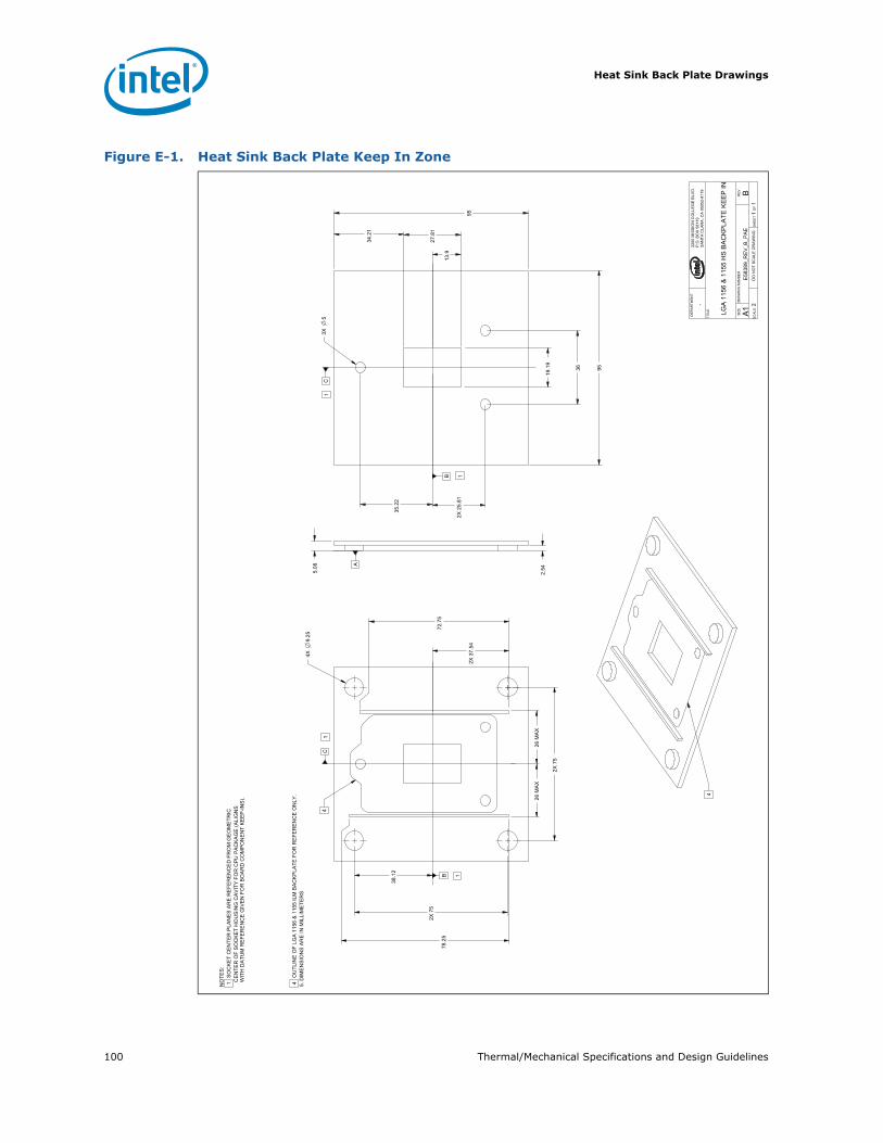
Heat Sink Back Plate Drawings
100 Thermal/Mechanical Specifications and Design Guidelines
Figure E-1. Heat Sink Back Plate Keep In Zone
2X
75
2X
75
38.1
2
78.2
5
19.1
9
27.8
1
95
95
13.9
34.2
1
5.0
8
2.5
4
72.7
5
2X
37.5
4
26 M
AX
26 M
AX
2X
25.8
1
35.2
2
36
3X
5
4X
9.2
5
B
A
B
CC
DE
PA
RT
ME
NT
R2200 M
ISS
ION
CO
LLE
GE
BLV
D.
P.O
. B
OX
58119
SA
NT
A C
LA
RA
, C
A 9
5052-8
119
-
TIT
LE
LG
A 1
156 &
1155 H
S B
AC
KP
LA
TE
KE
EP
IN
SIZ
E D
RA
WIN
G N
UM
BE
RR
EV
A1
E58389_R
EV
_B
_P
AE
BS
CA
LE
:2
DO
NO
T S
CA
LE
DR
AW
ING
SH
EE
T1
OF
1
NO
TE
S:
1 S
OC
KE
T C
EN
TE
R P
LA
NE
S A
RE
RE
FE
RE
NC
ED
FR
OM
GE
OM
ET
RIC
C
EN
TE
R O
F S
OC
KE
T H
OU
SIN
G C
AV
ITY
FO
R C
PU
PA
CK
AG
E (
ALIG
NS
W
ITH
DA
TU
M R
EF
ER
EN
CE
GIV
EN
FO
R B
OA
RD
CO
MP
ON
EN
T K
EE
P-I
NS
).3. LG
A 1
156 &
1155 H
S B
AC
KP
LA
TE
KE
EP
-IN
VO
LU
ME
EN
CO
MP
AS
S T
HE
BA
CK
PLA
TE
NO
MIN
AL V
OLU
ME
A
ND
ALLO
WA
NC
ES
FO
R S
IZE
TO
LE
RA
NC
ES
. T
HE
RM
AL/M
EC
HA
NIC
AL C
OM
PO
NE
NT
D
EV
ELO
PE
RS
SH
ALL D
ES
IGN
TO
TH
E O
UT
SID
E O
F S
OC
KE
T H
1 ILM
BA
CK
PLA
TE
4
W
ITH
CLE
AR
AN
CE
MA
RG
INS
. R
EF
ER
EN
CE
DR
AW
ING
S:
E
20847 -
LG
A 1
156 &
1155 ILM
BA
CK
PLA
TE
E
21320 -
LG
A 1
156 &
1155 ILM
&
PR
OC
ES
SO
R K
EE
PIN
4 O
UT
LIN
E O
F L
GA
1156 &
1155 ILM
BA
CK
PLA
TE
FO
R R
EF
ER
EN
CE
ON
LY
.
5. D
IME
NS
ION
S A
RE
IN
MIL
LIM
ET
ER
S
1
11
1
4
4
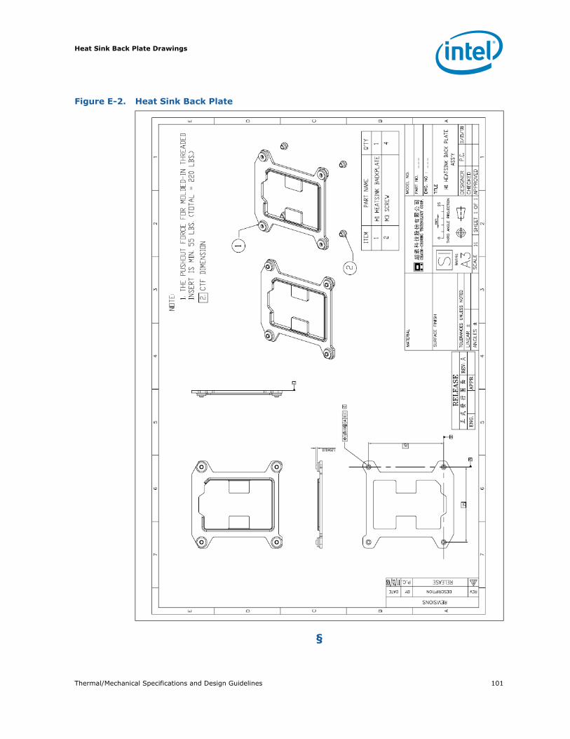
Thermal/Mechanical Specifications and Design Guidelines 101
Heat Sink Back Plate Drawings
§
Figure E-2. Heat Sink Back Plate

Heat Sink Back Plate Drawings
102 Thermal/Mechanical Specifications and Design Guidelines