Embed Size (px)
Citation preview
Integrating HDI Technologies
with Rigid-flex
Presenter: Bill Beckenbaugh, PhD
VP, Design & Engineering Multek
11/16/2011
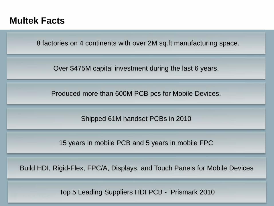
Produced more than 600M PCB pcs for Mobile Devices.
Shipped 61M handset PCBs in 2010
15 years in mobile PCB and 5 years in mobile FPC
8 factories on 4 continents with over 2M sq.ft manufacturing space.
Top 5 Leading Suppliers HDI PCB - Prismark 2010
Build HDI, Rigid-Flex, FPC/A, Displays, and Touch Panels for Mobile Devices
Over $475M capital investment during the last 6 years.
Multek Facts

Every Layer Interconnect(ELIC)
& Rigid-flex Market Outlook
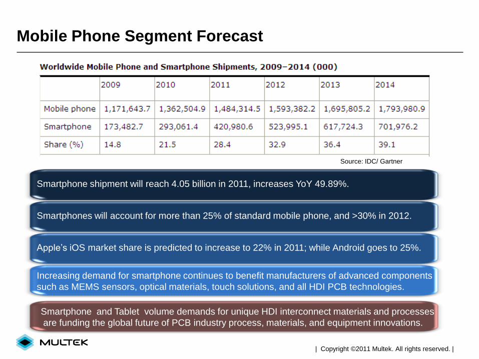
Mobile Phone Segment Forecast
Smartphone shipment will reach 4.05 billion in 2011, increases YoY 49.89%.
Smartphones will account for more than 25% of standard mobile phone, and >30% in 2012.
Apple’s iOS market share is predicted to increase to 22% in 2011; while Android goes to 25%.
Increasing demand for smartphone continues to benefit manufacturers of advanced components
such as MEMS sensors, optical materials, touch solutions, and all HDI PCB technologies.
Source: IDC/ Gartner
Smartphone and Tablet volume demands for unique HDI interconnect materials and processes
are funding the global future of PCB industry process, materials, and equipment innovations.
| Copyright ©2011 Multek. All rights reserved. |
5
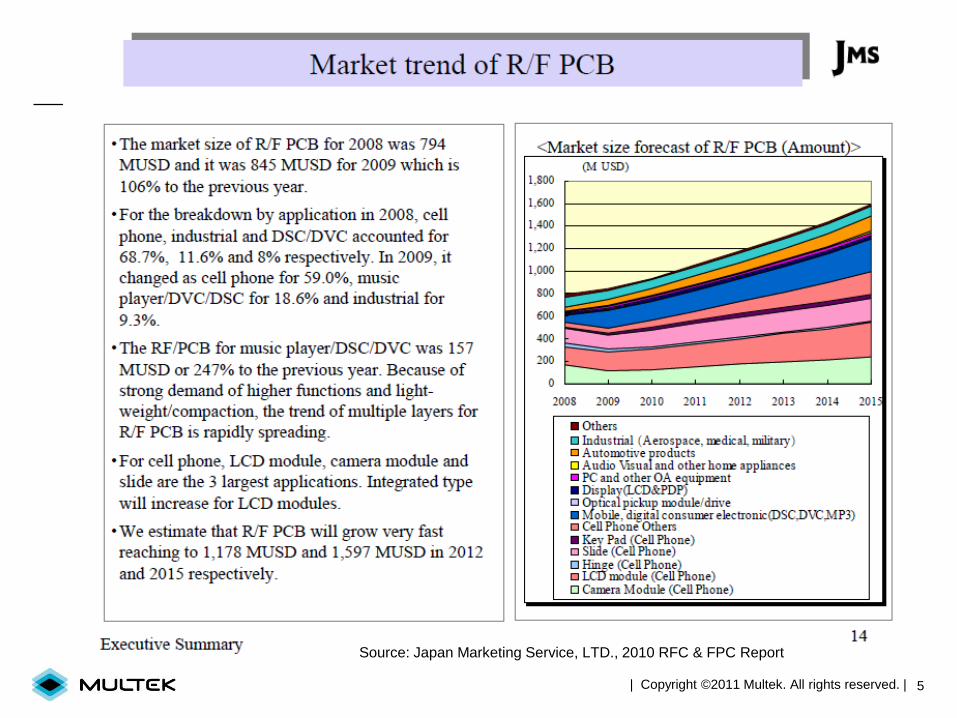
Source: Japan Marketing Service, LTD., 2010 RFC & FPC Report
| Copyright ©2011 Multek. All rights reserved. |

Technology Drivers in Portables
7
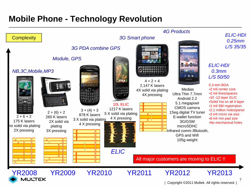
Mobile Phone - Technology Revolution
10L ELIC
1217 K lasers
5 X solid via plating
4 X pressing
4 + 2 + 4
2,147 K lasers
4X solid via plating
4X pressing
3 + (4) + 3
878 K lasers
3 X solid via plating
4 X pressing
Complexity
YR2008 YR2009 YR2010 YR2011 YR2012 YR2013
2 + 6 + 2
175 K lasers
no solid via plating
2X pressing
2 + (6) + 2
260 K lasers
2X solid via
plating
3X pressing
All major customers are moving to ELIC !!
ELIC
Medias
Ultra Thin 7.7mm
Android 2.2
5.1 megapixel
CMOS camera
1Seg digital TV tuner
E-wallet function
3G/GSM
microSDHC
Infrared comm /Blutooth,
GPS and Wifi
105g weight
NB,3C,Mobile,MP3
Module, GPS
3G PDA combine GPS
3G Smart phone
4G Products
ELIC-HDI
0.3mm
L/S 50/50
ELIC-HDI
0.25mm
L/S 35/35
0.3 mm BGA
2 mil center core
2 mil lines/spaces
10 -12 layer ELIC
Solid Via on all 4 layer
1 mil SM registration
2.2 million holes/panel
3 mil micro via size
8 mil min pad size
No mechanical holes
| Copyright ©2011 Multek. All rights reserved. |
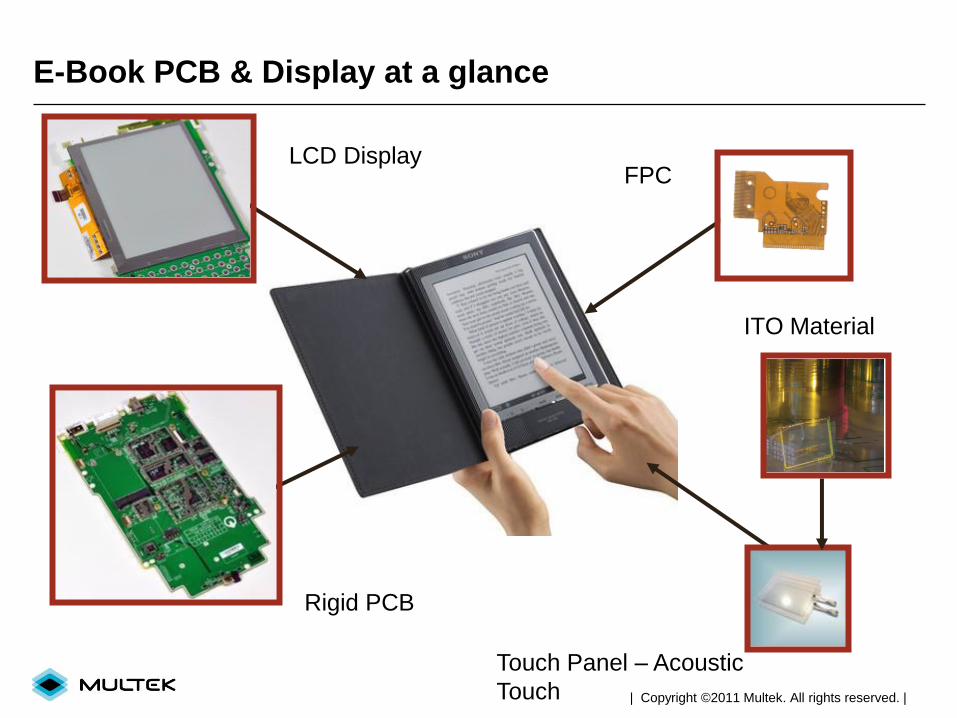
E-Book PCB & Display at a glance
LCD Display
Rigid PCB
Touch Panel – Acoustic
Touch
FPC
ITO Material
| Copyright ©2011 Multek. All rights reserved. |
9 | Copyright ©2011 Multek. All rights reserved. |
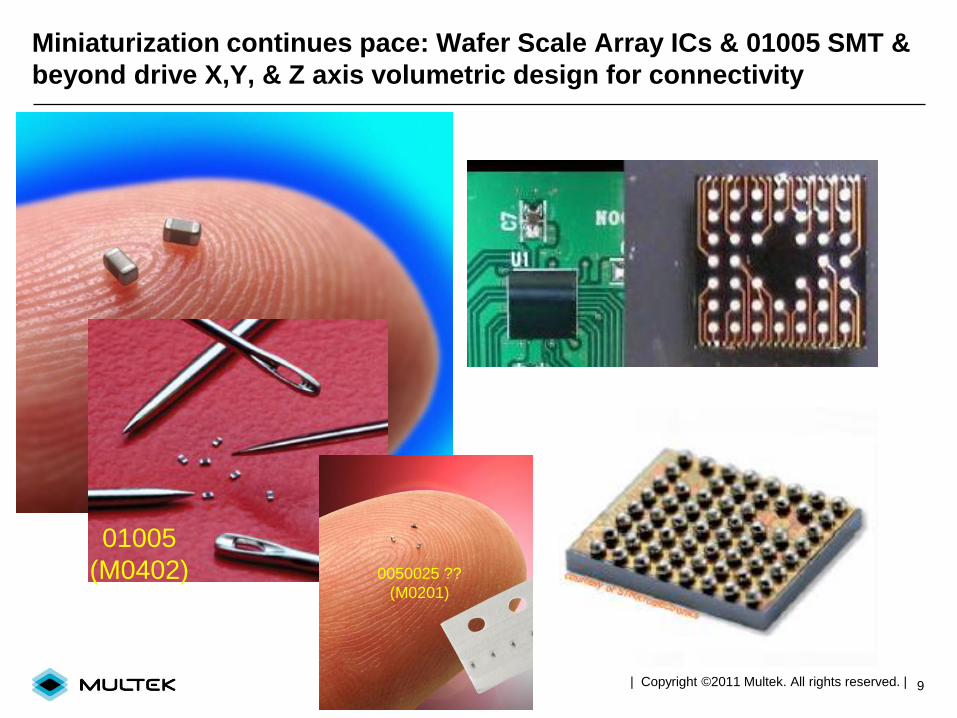
Miniaturization continues pace: Wafer Scale Array ICs & 01005 SMT &
beyond drive X,Y, & Z axis volumetric design for connectivity
01005
(M0402) 0050025 ??
(M0201)
CONFIDENTIAL | Copyright ©2011 Multek. All rights reserved.
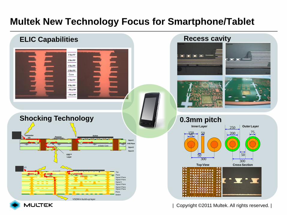
Recess cavity
75150
30050
50
50
250
200
300
75
Inner Layer Outer Layer
Top View Cross Section
0.3mm pitch
VSDM in build-up layer
XStatic
Top
Plane
Signal / Plane
Signal / Plane
I/O
Passive
Signal 3
Signal / Plane
Signal / PlaneSignal / Plane
Plane
Bottom
XStatic Core
Signal 1
VSD™
Layer
Connector
I/O
GND Plane
Signal 2
Signal 3
PassiveActive
Shocking Technology
ELIC Capabilities
Multek New Technology Focus for Smartphone/Tablet
| Copyright ©2011 Multek. All rights reserved. |
11
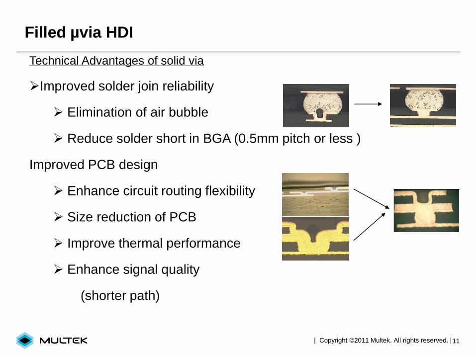
Filled µvia HDI
Technical Advantages of solid via
Improved solder join reliability
Elimination of air bubble
Reduce solder short in BGA (0.5mm pitch or less )
Improved PCB design
Enhance circuit routing flexibility
Size reduction of PCB
Improve thermal performance
Enhance signal quality
(shorter path)
| Copyright ©2011 Multek. All rights reserved. |

ELIC and FPC Development
for Rigid-flex
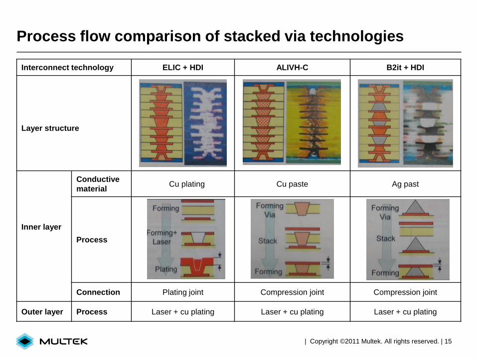
Process flow comparison of stacked via technologies
Interconnect technology ELIC + HDI ALIVH-C B2it + HDI
Layer structure
Inner layer
Conductive
material Cu plating Cu paste Ag past
Process
Connection Plating joint Compression joint Compression joint
Outer layer Process Laser + cu plating Laser + cu plating Laser + cu plating
| Copyright ©2011 Multek. All rights reserved. | 15
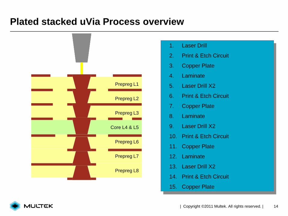
Plated stacked uVia Process overview
14 | Copyright ©2011 Multek. All rights reserved. |
L4 L3 L2
Prepreg L8
Prepreg L1
Prepreg L2
Prepreg L7
Prepreg L6
Prepreg L3
Core L4 & L5
L1 1. Laser Drill
2. Print & Etch Circuit
3. Copper Plate
4. Laminate
5. Laser Drill X2
6. Print & Etch Circuit
7. Copper Plate
8. Laminate
9. Laser Drill X2
10. Print & Etch Circuit
11. Copper Plate
12. Laminate
13. Laser Drill X2
14. Print & Etch Circuit
15. Copper Plate
cu1
tcu2
bcu2
bcu3
tcu3
tcu4
bcu4
15 | Copyright ©2011 Multek. All rights reserved. |
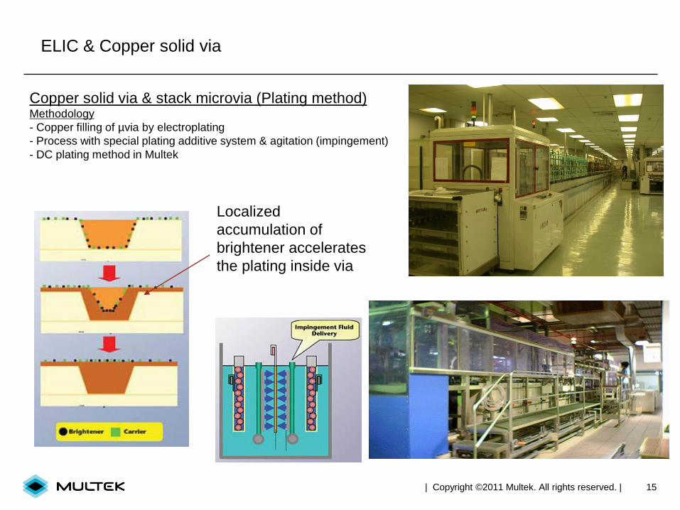
ELIC & Copper solid via
Copper solid via & stack microvia (Plating method) Methodology
- Copper filling of µvia by electroplating
- Process with special plating additive system & agitation (impingement)
- DC plating method in Multek
Localized
accumulation of
brightener accelerates
the plating inside via
16 | Copyright ©2011 Multek. All rights reserved. |
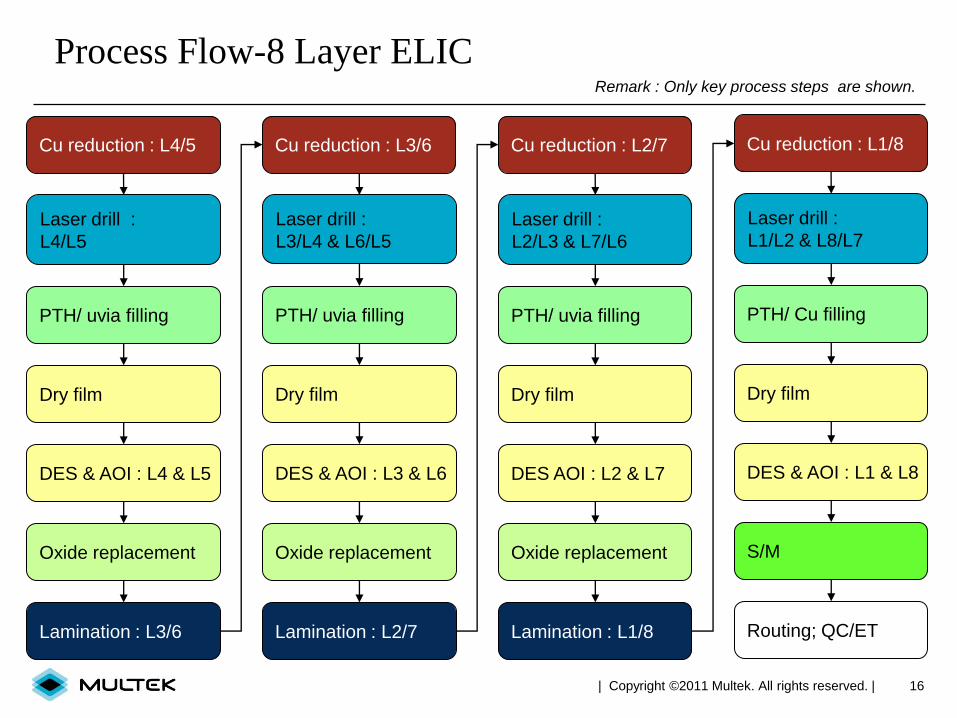
Process Flow-8 Layer ELIC
Cu reduction : L4/5
Laser drill :
L4/L5
PTH/ uvia filling
Dry film
DES & AOI : L4 & L5
Oxide replacement
Lamination : L3/6
Cu reduction : L3/6
Laser drill :
L3/L4 & L6/L5
PTH/ uvia filling
Dry film
DES & AOI : L3 & L6
Oxide replacement
Lamination : L2/7
Cu reduction : L2/7
Laser drill :
L2/L3 & L7/L6
PTH/ uvia filling
Dry film
DES AOI : L2 & L7
Oxide replacement
Lamination : L1/8
Cu reduction : L1/8
Laser drill :
L1/L2 & L8/L7
PTH/ Cu filling
Dry film
DES & AOI : L1 & L8
S/M
Routing; QC/ET
Remark : Only key process steps are shown.
17
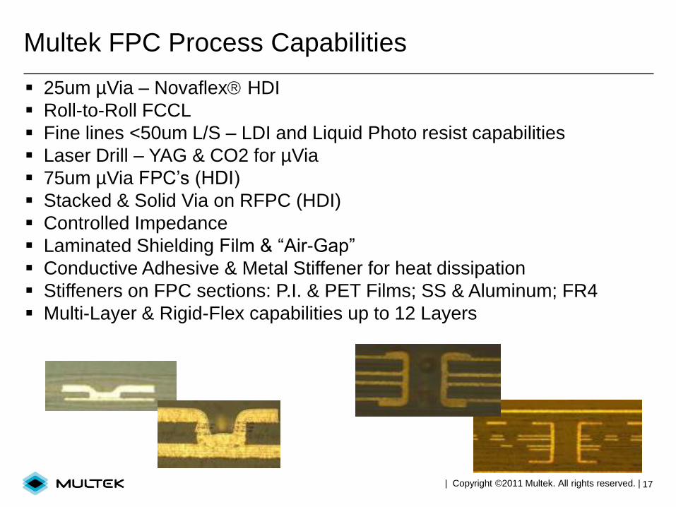
Multek FPC Process Capabilities
25um µVia – Novaflex HDI
Roll-to-Roll FCCL
Fine lines <50um L/S – LDI and Liquid Photo resist capabilities
Laser Drill – YAG & CO2 for µVia
75um µVia FPC’s (HDI)
Stacked & Solid Via on RFPC (HDI)
Controlled Impedance
Laminated Shielding Film & “Air-Gap”
Conductive Adhesive & Metal Stiffener for heat dissipation
Stiffeners on FPC sections: P.I. & PET Films; SS & Aluminum; FR4
Multi-Layer & Rigid-Flex capabilities up to 12 Layers
| Copyright ©2011 Multek. All rights reserved. |
18
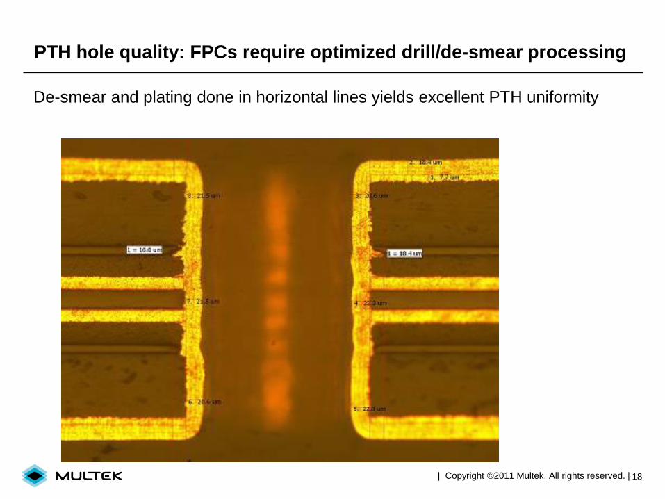
PTH hole quality: FPCs require optimized drill/de-smear processing
De-smear and plating done in horizontal lines yields excellent PTH uniformity
| Copyright ©2011 Multek. All rights reserved. |
XStatic: A Voltage Switchable Dielectric™ (VSD™)
“ Polymer Diode”
Shocking Technologies
19
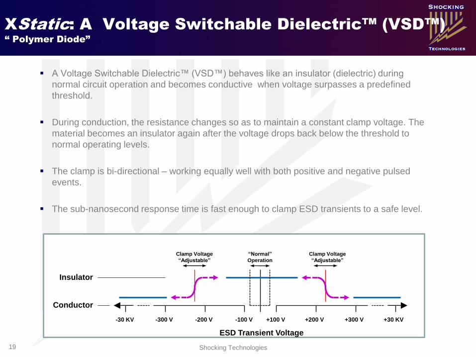
A Voltage Switchable Dielectric™ (VSD™) behaves like an insulator (dielectric) during
normal circuit operation and becomes conductive when voltage surpasses a predefined
threshold.
During conduction, the resistance changes so as to maintain a constant clamp voltage. The
material becomes an insulator again after the voltage drops back below the threshold to
normal operating levels.
The clamp is bi-directional – working equally well with both positive and negative pulsed
events.
The sub-nanosecond response time is fast enough to clamp ESD transients to a safe level.
Insulator
Conductor
ESD Transient Voltage
+100 V +200 V +300 V +30 KV
Clamp Voltage
“Adjustable”
-100 V -200 V -300 V -30 KV
Clamp Voltage
“Adjustable”
“Normal”
Operation
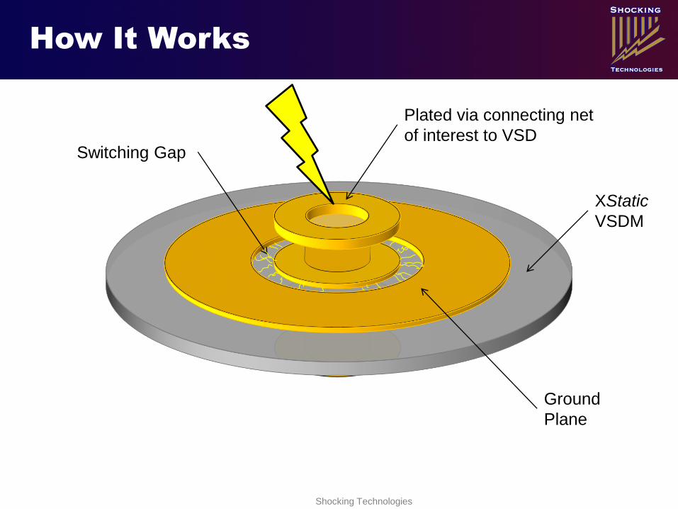
XStatic
VSDM
Plated via connecting net
of interest to VSD Switching Gap
Ground
Plane
How It Works
Shocking Technologies
21
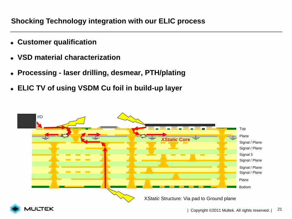
Customer qualification
VSD material characterization
Processing - laser drilling, desmear, PTH/plating
ELIC TV of using VSDM Cu foil in build-up layer
XStatic Structure: Via pad to Ground plane
XStatic Core
Top
Plane
Signal / Plane
Signal / Plane
I/O
Passive
Signal 3
Signal / Plane
Signal / Plane
Signal / Plane
Plane
Bottom
Shocking Technology integration with our ELIC process
| Copyright ©2011 Multek. All rights reserved. |

Rigid Flex Roadmap
23
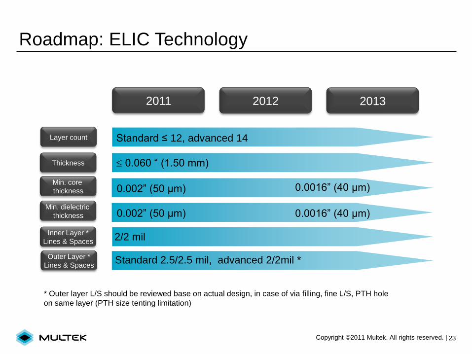
Roadmap: ELIC Technology
2011 2012 2013
Layer count
Thickness
Min. core
thickness
Inner Layer *
Lines & Spaces
Outer Layer *
Lines & Spaces
Standard ≤ 12, advanced 14
0.060 “ (1.50 mm)
0.002” (50 µm)
2/2 mil
Standard 2.5/2.5 mil, advanced 2/2mil *
Copyright ©2011 Multek. All rights reserved. |
Min. dielectric
thickness 0.002” (50 µm)
* Outer layer L/S should be reviewed base on actual design, in case of via filling, fine L/S, PTH hole
on same layer (PTH size tenting limitation)
0.0016” (40 µm)
0.0016” (40 µm)
24
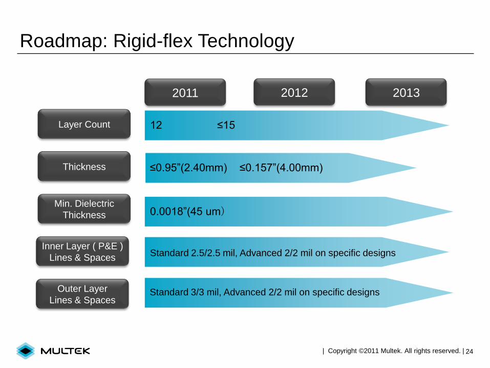
Roadmap: Rigid-flex Technology
2011 2012 2013
Layer Count
≤0.95”(2.40mm) ≤0.157”(4.00mm)
| Copyright ©2011 Multek. All rights reserved. |
Thickness
Min. Dielectric
Thickness
Inner Layer ( P&E )
Lines & Spaces
Outer Layer
Lines & Spaces
12 ≤15
0.0018”(45 um)
Standard 2.5/2.5 mil, Advanced 2/2 mil on specific designs
Standard 3/3 mil, Advanced 2/2 mil on specific designs
25
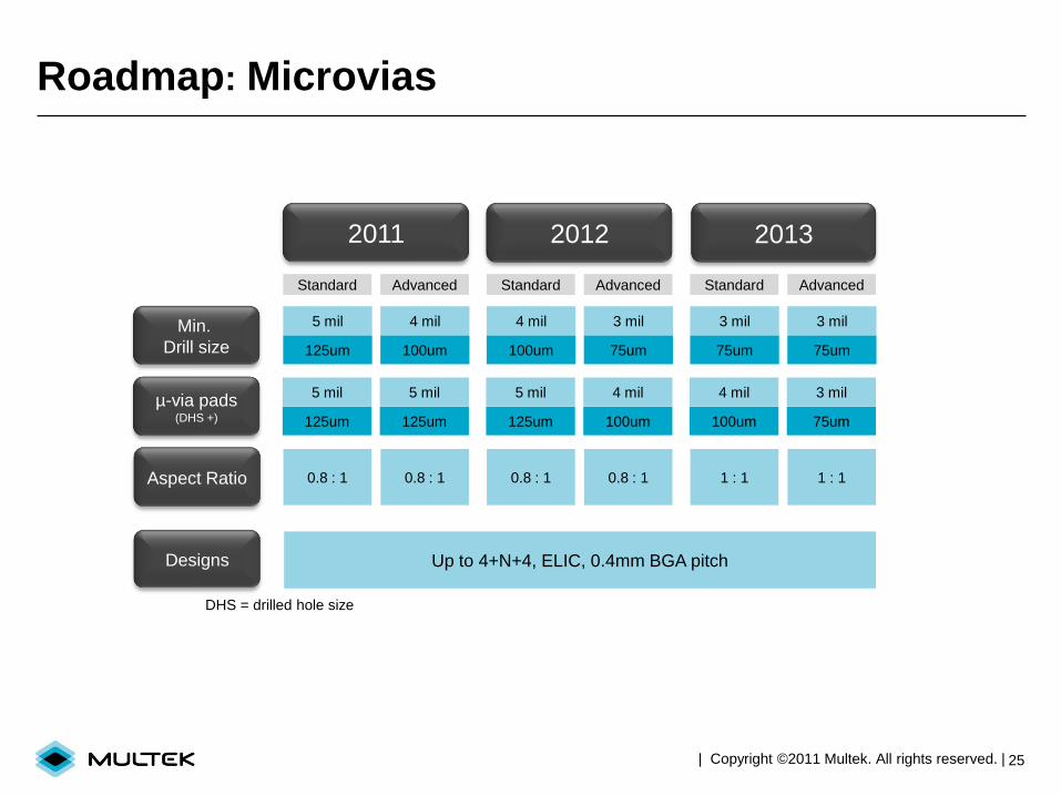
5 mil
125um
0.8 : 1
Min.
Drill size
µ-via pads (DHS +)
Aspect Ratio
Up to 4+N+4, ELIC, 0.4mm BGA pitch Designs
Roadmap: Microvias
2011 2012 2013
Standard Advanced Standard Advanced Standard Advanced
0.8 : 1 0.8 : 1 0.8 : 1 1 : 1 1 : 1
5 mil
125um
5 mil
125um
4 mil
100um
4 mil
100um
3 mil
75um
5 mil
125um
4 mil
100um
4 mil
100um
3 mil
75um
3 mil
75um
3 mil
75um
DHS = drilled hole size
| Copyright ©2011 Multek. All rights reserved. |
26
Soldermask
Registration
Soldermask
dam
Legend ink
Soldermask
Standard (green): Taiyo PSR 4000 Z26/G23K/MP/SP08
Halogen free (black): Taiyo PSR 4000 EG23 / PSR 2000 ME8H
Halogen free (blue): Taiyo PSR 4000 GP01/BL01/SP13
Halogen free (green): Taiyo PSR 4000 GEC50
Roadmap: Soldermask & Graphics
2011 2012 2013
Standard Advanced Standard Advanced Standard Advanced
1.5 mil
38um
1.5 mil
38um
1.5 mil
38 um
1 mil
25um
1 mil
25um
1 mil
25um
3 mil
75um
2.4 mil
60um*
2.4 mil
60um
2 mil
50um
2 mil
50um
2 mil
50um
4mil / 100um line width (legend printer)
6 mil / 150 µm line width (screen printer)
* For black soldermask, min. dam is 60um for BGA and 100um for bridge between fingers.
| Copyright ©2011 Multek. All rights reserved. |
27
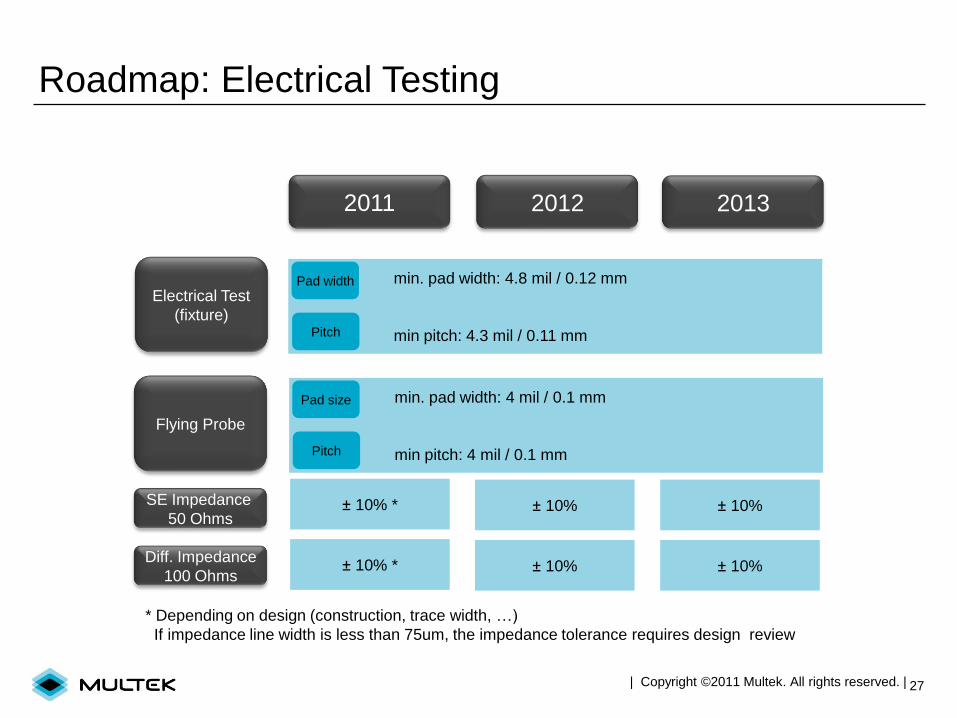
min. pad width: 4 mil / 0.1 mm
min pitch: 4 mil / 0.1 mm
Roadmap: Electrical Testing
SE Impedance
50 Ohms
Diff. Impedance
100 Ohms
2011 2012 2013
Flying Probe
Electrical Test
(fixture)
min. pad width: 4.8 mil / 0.12 mm
min pitch: 4.3 mil / 0.11 mm
Pad size
Pitch
Pad width
Pitch
± 10% ± 10% ± 10% *
± 10% ± 10% ± 10% *
* Depending on design (construction, trace width, …)
If impedance line width is less than 75um, the impedance tolerance requires design review
| Copyright ©2011 Multek. All rights reserved. |

Conventional PTH Rigid-flex
Product Examples
29
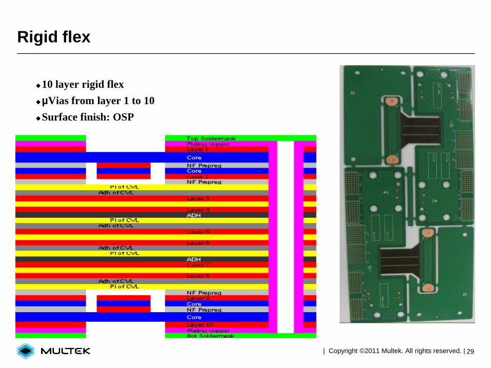
Rigid flex
10 layer rigid flex
µVias from layer 1 to 10
Surface finish: OSP
| Copyright ©2011 Multek. All rights reserved. |
30
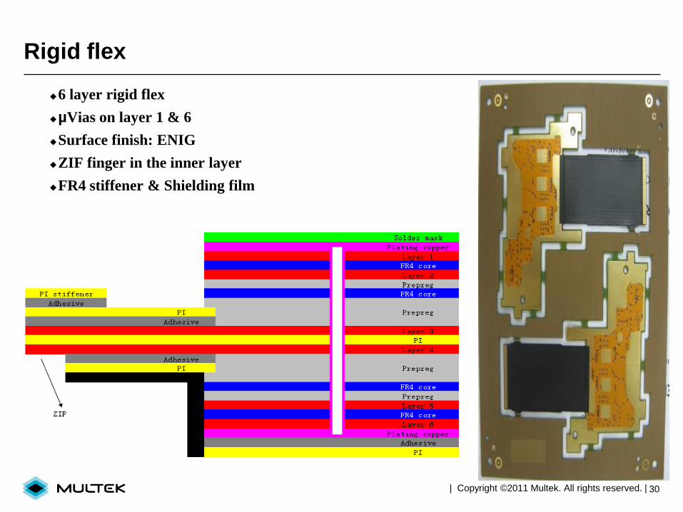
Rigid flex
6 layer rigid flex
µVias on layer 1 & 6
Surface finish: ENIG
ZIF finger in the inner layer
FR4 stiffener & Shielding film
| Copyright ©2011 Multek. All rights reserved. |
31
Rigid flex
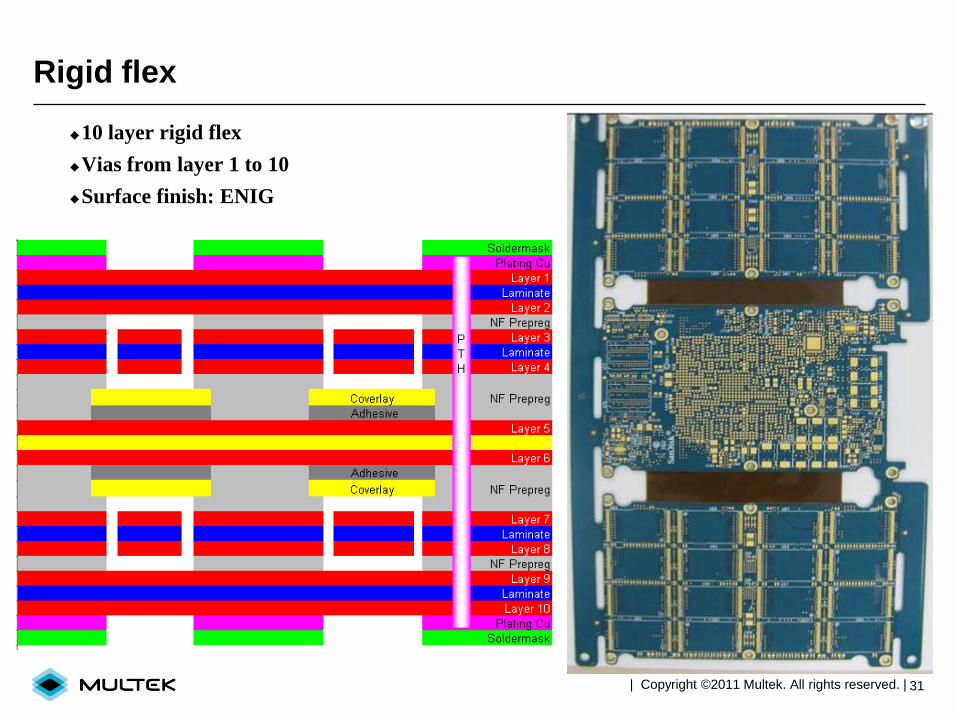
10 layer rigid flex
Vias from layer 1 to 10
Surface finish: ENIG
| Copyright ©2011 Multek. All rights reserved. |
Next-gen Rigid-flex based on
ELIC HDI and advanced FPC
Technologies
33
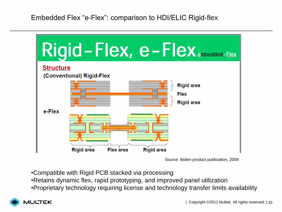
Embedded Flex “e-Flex”: comparison to HDI/ELIC Rigid-flex
Source: Ibiden product publication, 2009
•Compatible with Rigid PCB stacked via processing
•Retains dynamic flex, rapid prototyping, and improved panel utilization
•Proprietary technology requiring license and technology transfer limits availability
| Copyright ©2011 Multek. All rights reserved. |
34
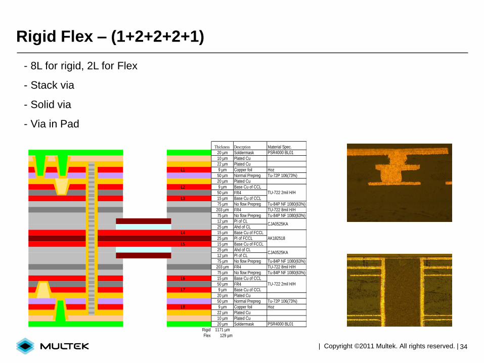
Rigid Flex – (1+2+2+2+1)
Thickness Descrption Material Spec.
20 µm Soldermask PSR4000 BL01
10 µm Plated Cu
22 µm Plated Cu
L1 9 µm Copper foil Hoz
50 µm Normal Prepreg Tu-72P 106(73%)
20 µm Plated Cu
L2 9 µm Base Cu of CCL
50 µm FR4
L3 15 µm Base Cu of CCL
75 µm No flow Prepreg Tu-84P NF 1080(63%)
203 µm FR4 TU-722 8mil H/H
75 µm No flow Prepreg Tu-84P NF 1080(63%)
12 µm PI of CL
25 µm Ahd of CL
L4 15 µm Base Cu of FCCL
25 µm PI of FCCL
L5 15 µm Base Cu of FCCL
25 µm Ahd of CL
12 µm PI of CL
75 µm No flow Prepreg Tu-84P NF 1080(63%)
203 µm FR4 TU-722 8mil H/H
75 µm No flow Prepreg Tu-84P NF 1080(63%)
L6 15 µm Base Cu of CCL
50 µm FR4
L7 9 µm Base Cu of CCL
20 µm Plated Cu
50 µm Normal Prepreg Tu-72P 106(73%)
L8 9 µm Copper foil Hoz
22 µm Plated Cu
10 µm Plated Cu
20 µm Soldermask PSR4000 BL01
Rigid 1171 µm
Flex 129 µm
TU-722 2mil H/H
TU-722 2mil H/H
CJA0525KA
CJA0525KA
AK182518
- 8L for rigid, 2L for Flex
- Stack via
- Solid via
- Via in Pad
| Copyright ©2011 Multek. All rights reserved. |
35
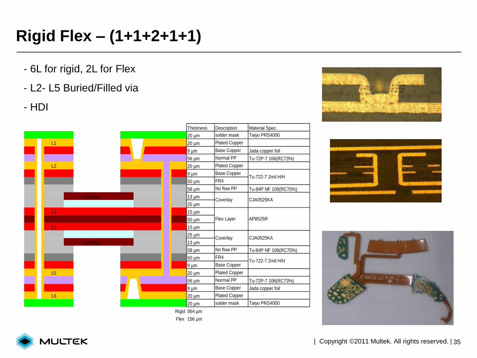
Rigid Flex – (1+1+2+1+1)
- 6L for rigid, 2L for Flex
- L2- L5 Buried/Filled via
- HDI
Thickness Description Material Spec.
20 µm solder mask Taiyo PRS4000
L1 20 µm Plated Copper
9 µm Base Copper Jada copper foil
56 µm Normal PP Tu-72P-7 106(RC73%)
L2 20 µm Plated Copper
9 µm Base Copper
50 µm FR4
58 µm No flow PP Tu-84P NF 106(RC70%)
Coverlay 13 µm
25 µm
L3 15 µm
50 µm
L4 15 µm
25 µm
Coverlay 13 µm
58 µm No flow PP Tu-84P NF 106(RC70%)
50 µm FR4
9 µm Base Copper
L5 20 µm Plated Copper
56 µm Normal PP Tu-72P-7 106(RC73%)
9 µm Base Copper Jada copper foil
L6 20 µm Plated Copper
20 µm solder mask Taiyo PRS4000
Rigid 564 µm
Flex 156 µm
Coverlay
Flex Layer
Coverlay
AP8525R
Tu-722-7 2mil H/H
Tu-722-7 2mil H/H
CJA0525KA
CJA0525KA
| Copyright ©2011 Multek. All rights reserved. |
36 ©2011 Multek. All rights reserved. |
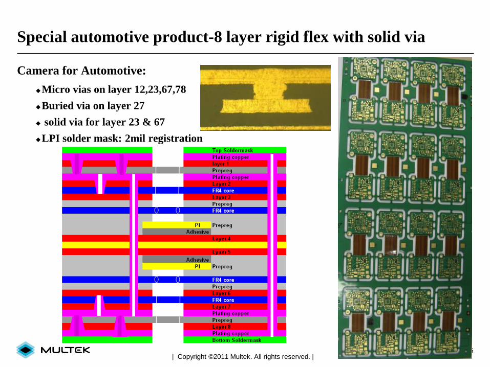
Special automotive product-8 layer rigid flex with solid via
Camera for Automotive:
Micro vias on layer 12,23,67,78
Buried via on layer 27
solid via for layer 23 & 67
LPI solder mask: 2mil registration
| Copyright ©2011 Multek. All rights reserved. |
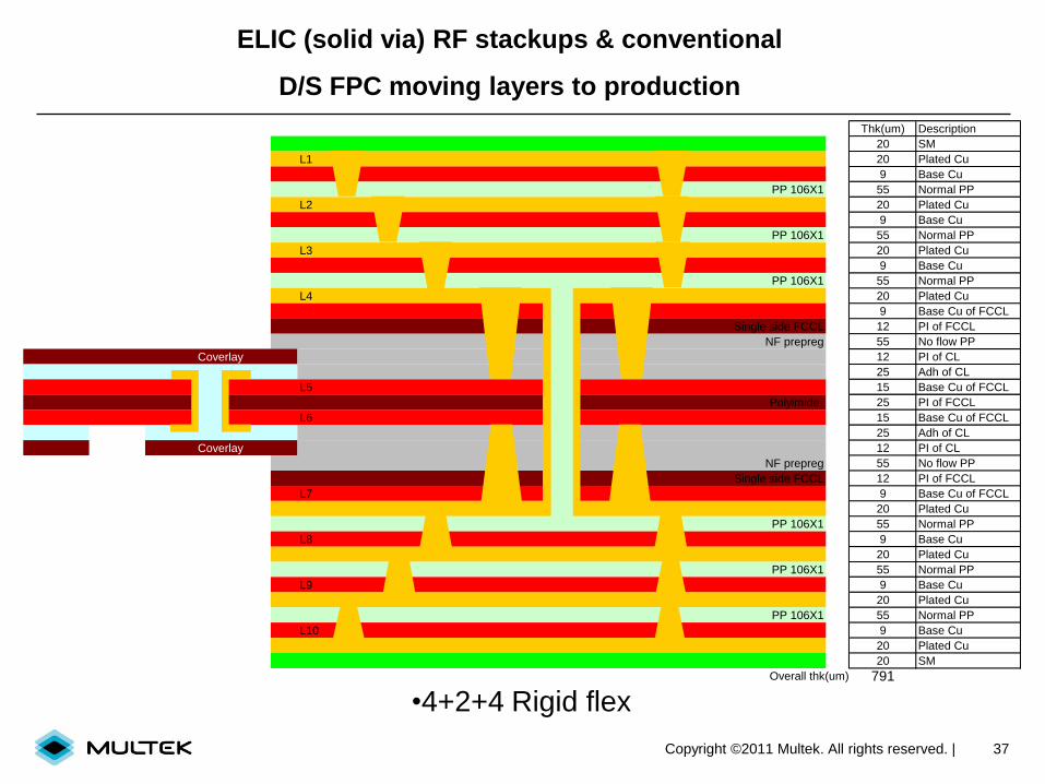
37 Copyright ©2011 Multek. All rights reserved. |
ELIC (solid via) RF stackups & conventional
D/S FPC moving layers to production
•4+2+4 Rigid flex
Thk(um) Description
20 SM
L1 20 Plated Cu
9 Base Cu
PP 106X1 55 Normal PP
L2 20 Plated Cu
9 Base Cu
PP 106X1 55 Normal PP
L3 20 Plated Cu
9 Base Cu
PP 106X1 55 Normal PP
L4 20 Plated Cu
9 Base Cu of FCCL
Single side FCCL 12 PI of FCCL
NF prepreg 55 No flow PP
Coverlay 12 PI of CL
25 Adh of CL
L5 15 Base Cu of FCCL
Polyimide 25 PI of FCCL
L6 15 Base Cu of FCCL
25 Adh of CL
Coverlay 12 PI of CL
NF prepreg 55 No flow PP
Single side FCCL 12 PI of FCCL
L7 9 Base Cu of FCCL
20 Plated Cu
PP 106X1 55 Normal PP
L8 9 Base Cu
20 Plated Cu
PP 106X1 55 Normal PP
L9 9 Base Cu
20 Plated Cu
PP 106X1 55 Normal PP
L10 9 Base Cu
20 Plated Cu
20 SM
Overall thk(um) 791
38 ©2011 Multek. All rights reserved. |
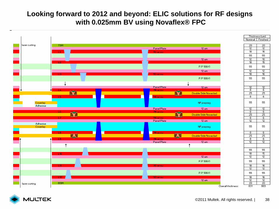
Looking forward to 2012 and beyond: ELIC solutions for RF designs
with 0.025mm BV using Novaflex® FPC
Summary
•Global market demand for Smartphones
and Tablets have accelerated (and funded)
the technology development of stacked
µvias and associated mass production
infrastructure.
•Filled via technologies are now essential
PCB fabrication processes to achieve high
SMT yield and reliability for Area Array IC
package and fine pitch passive
components assembly.
•Filled and stacked µvia sequential
processing is maturing to very high yields.
•Rigid-flex PCB technology using ELIC is
receiving increased emphasis in new
product designs to achieve:
• Higher volumetric interconnection of
components and structural featuring within the
PCB.
• Elimination of traditional connectors and ACF
bonding FPCs to rigid PCBs with inherent cost
and reliability issues.
• Laminate, Materials, Chemistry, and
Equipment suppliers roadmaps are on track to
provide compatible LF/HF materials and µvia
process systems for Rigid-flex to move to
mainstream.
39 Copyright ©2011 Multek. All rights reserved. |
Acknowledgements
Many thanks for the support and many technical contributions from:
Multek Field Application Engineers:
Tony Cosentino, Victor Llanes, Pedro Macias, Todd Robinson, and
Dan Slocum
Multek Flex Circuits Engineering:
Simpson Chan
Multek Doumen Advanced Development Engineering:
Jim Poon, TM Chan and Marie Yu
Multek Doumen-Process Engineering-:
Simon Au and James Leung
40 | Copyright ©2011 Multek. All rights reserved. |


![Tech 2) Active Optical · camera module, (f), and (g) FPCs to LCD IC and digitizer [15]. Figure 4. Schematic of the OE-Rigid/Flex HDI test vehicle with two rigid OE Modules (Board1](https://img.dokumen.tips/doc/110x75/6019d8869597ba706d772073/tech-2-active-camera-module-f-and-g-fpcs-to-lcd-ic-and-digitizer-15-figure.jpg)