Embed Size (px)
Citation preview

1
Input/Output
Devices
Lecturer: Sri Parameswaran
Notes by: Annie Guo
2
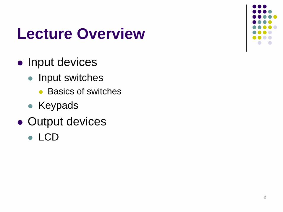
Lecture Overview
⚫ Input devices
⚫ Input switches
⚫ Basics of switches
⚫ Keypads
⚫ Output devices
⚫ LCD
3
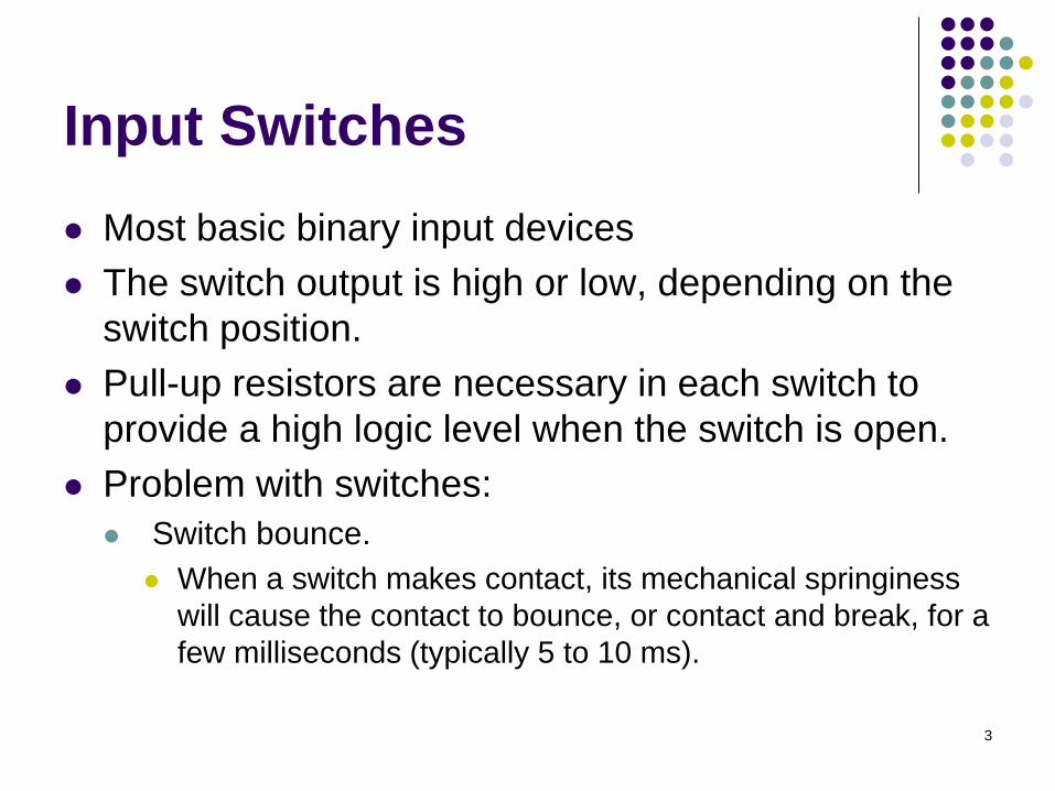
Input Switches
⚫ Most basic binary input devices
⚫ The switch output is high or low, depending on the
switch position.
⚫ Pull-up resistors are necessary in each switch to
provide a high logic level when the switch is open.
⚫ Problem with switches:
⚫ Switch bounce.
⚫ When a switch makes contact, its mechanical springiness
will cause the contact to bounce, or contact and break, for a
few milliseconds (typically 5 to 10 ms).
4
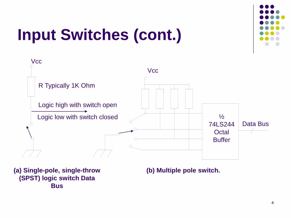
Data Bus½
74LS244
Octal
Buffer
Vcc
(a) Single-pole, single-throw
(SPST) logic switch Data
Bus
(b) Multiple pole switch.
R Typically 1K Ohm
Logic high with switch open
Logic low with switch closed
Input Switches (cont.)
Vcc
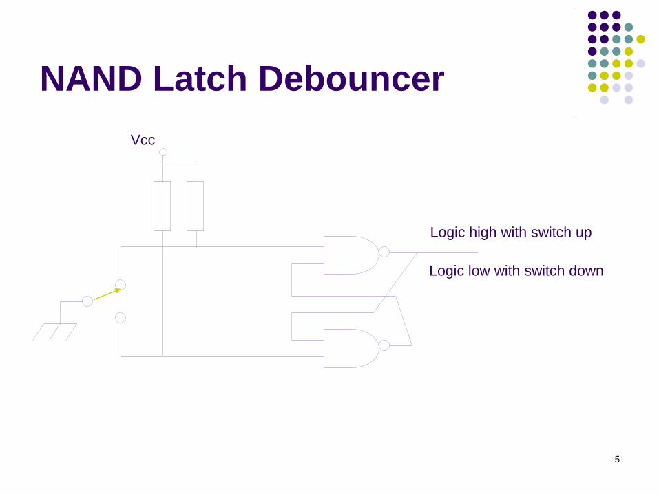
5
Logic high with switch up
Logic low with switch down
Vcc
NAND Latch Debouncer
6
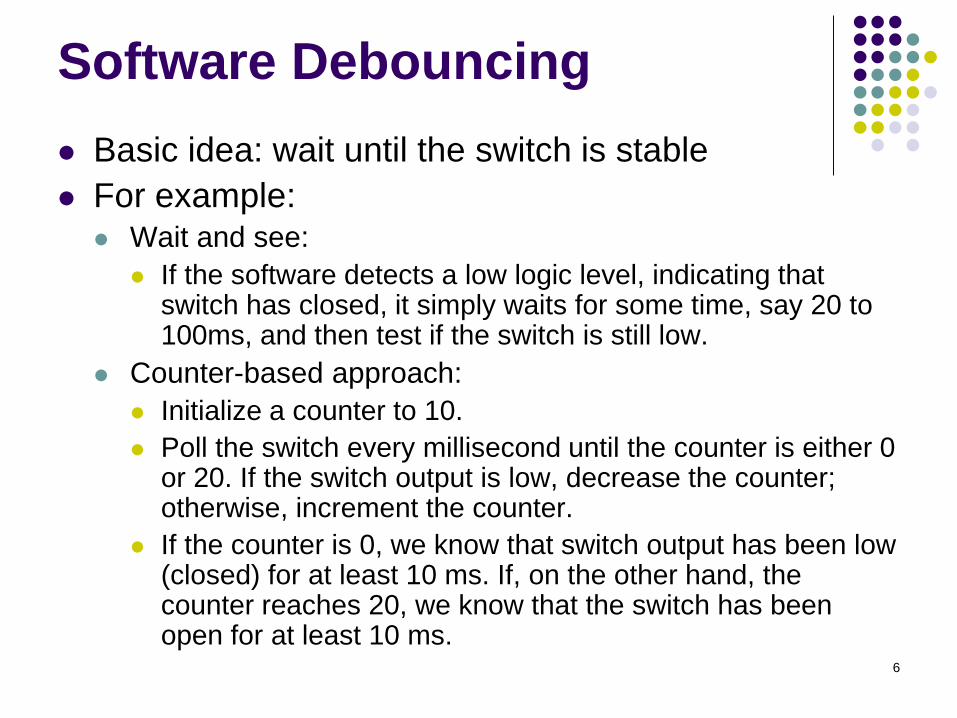
Software Debouncing
⚫ Basic idea: wait until the switch is stable
⚫ For example:⚫ Wait and see:
⚫ If the software detects a low logic level, indicating that switch has closed, it simply waits for some time, say 20 to 100ms, and then test if the switch is still low.
⚫ Counter-based approach:
⚫ Initialize a counter to 10.
⚫ Poll the switch every millisecond until the counter is either 0 or 20. If the switch output is low, decrease the counter; otherwise, increment the counter.
⚫ If the counter is 0, we know that switch output has been low (closed) for at least 10 ms. If, on the other hand, the counter reaches 20, we know that the switch has been open for at least 10 ms.
7
I0
I2
I3
I4
I5
I6
I7
I1
E S2 S1 S0
Selected Input From
Output Port
Z
Scanned
Switch Data
To Input Port
74LS151 8 to 1
Multiplexer
A
Vcc
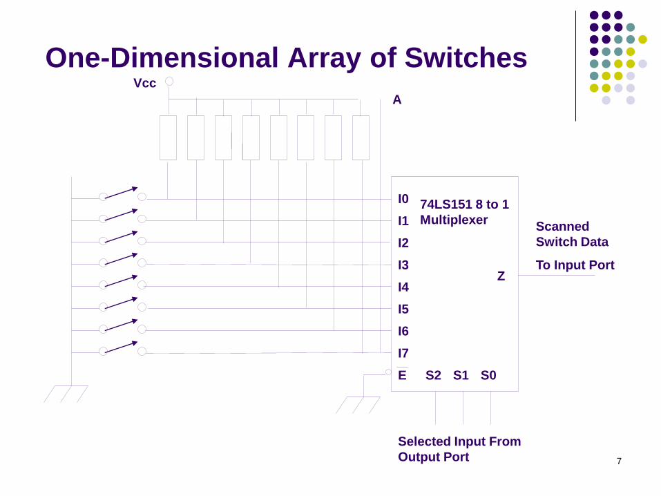
One-Dimensional Array of Switches
8
One-Dimensional Array of
Switches
⚫ Switch bouncing problem must be solved
⚫ Either using software or hardware
⚫ The array of switches must be scanned to
find out which switches are closed or open.
⚫ Software is required to scan the array. As the
software outputs a 3-bit sequence from 000 to
111, the multiplexer selects each of the switch
inputs.
⚫ The output of switch array could be interfaced
directly to an eight-bit port at point A.
9
I0
I2
I3
I4
I5
I6
I7
I1
ES2 S1 S0
Select Input From
Output Port
Z
Scanned Switch
Data
To Input Port
00 01 02 0706
10 11 12 17
70 71 77
O0 O1 O2 O3 O7O6O5O4
74LS151 8-to-1
Input
Multiplexer
A0A1A2E3 E2 E1
Vcc
B
A
Scan Input From Output Port
74LS138 3-of-8
Decoder
Vcc
12
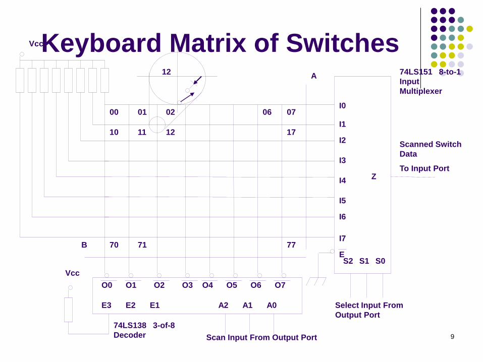
Keyboard Matrix of Switches
10
Keyboard Matrix of Switches
(cont.)
⚫ A keyboard is an array of switches arranged
in a two-dimensional matrix.
⚫ A switch is connected at each intersection of
vertical and horizontal lines.
⚫ Closing the switch connects the horizontal
line to the vertical line.
⚫ 8*8 keyboard can be interfaced directly into
8-bit output and input ports at point A and B.
11
Keyboard Matrix of Switches
(cont.)
⚫ Software can scan the key board by
outputting a three-bit code to the decoder and
then scanning the multiplexer to find the
closed switch or switches.
⚫ The combination of the two 3-bit scan codes
(A2A1A0 and S2S1S0) identifies which switch is
closed. For example, the code 000000 scan
switch 00 in the upper left-hand corner.
⚫ The diode prevents a problem called
ghosting.
12
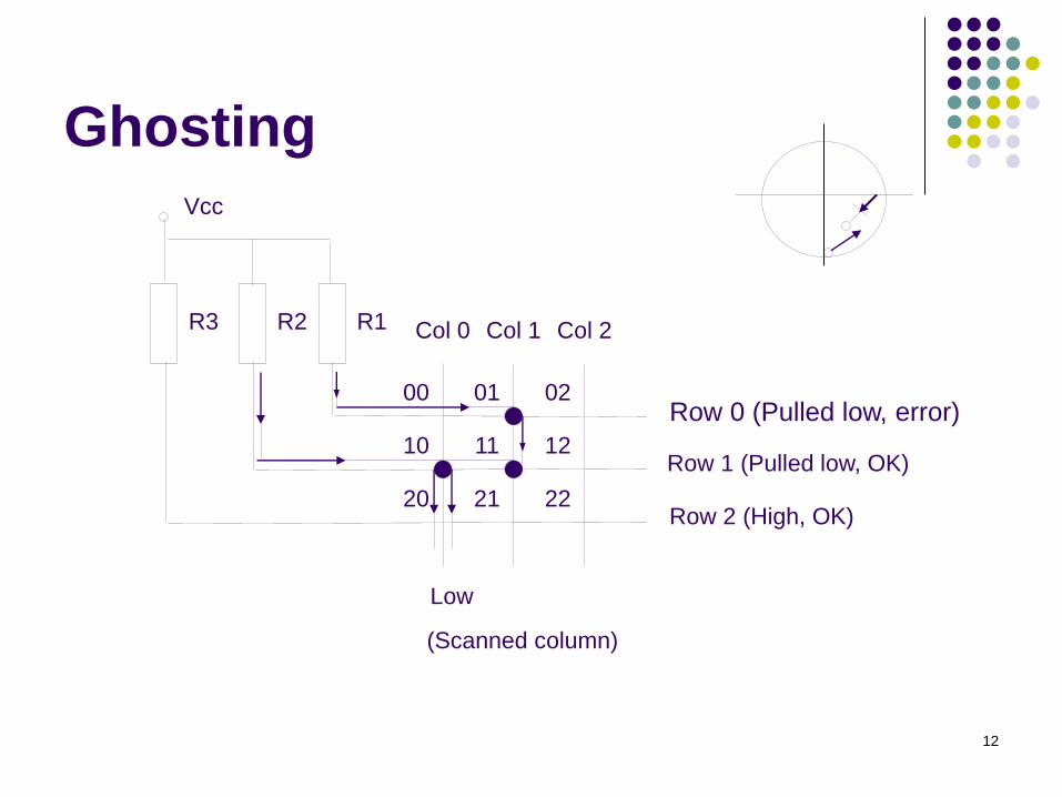
Col 0 Col 1 Col 2
00 01 02
10
20
11
21
12
22
R3 R2 R1
Row 0 (Pulled low, error)
Row 1 (Pulled low, OK)
Row 2 (High, OK)
Low
(Scanned column)
Vcc
Ghosting
13
Ghosting (cont.)
⚫ Ghosting occurs when several keys are pushed at once.
⚫ Consider the case shown in the figure where three switches 01, 10 and 11 are all closed. Column 0 is selected with a logic low and assume that the circuit does not contain the diodes. As the rows are scanned, a low is sensed on Row 1, which is acceptable because switch 10 is closed. In addition, Row 0 is seen to be low, indicating switch 00 is closed, which is NOT true. The diodes in the switches eliminate this problem by preventing current flow from R1 through switches 01 and 11. Thus Row 0 will not be low when it is scanned.
14
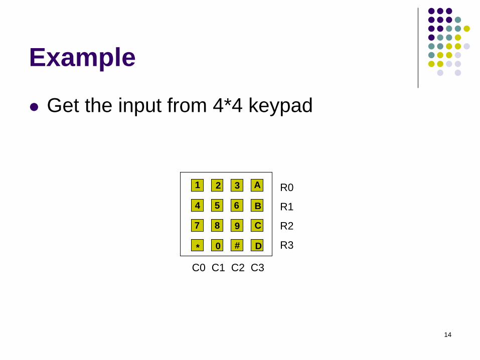
Example
⚫ Get the input from 4*4 keypad
C0 C1 C2 C3
R0
R1
R2
R3
1 A2 3
4 5 6
7 8 9
0* #
B
C
D
15
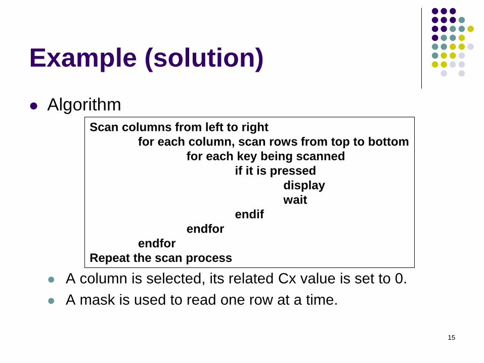
Example (solution)
⚫ Algorithm
⚫ A column is selected, its related Cx value is set to 0.
⚫ A mask is used to read one row at a time.
Scan columns from left to right
for each column, scan rows from top to bottom
for each key being scanned
if it is pressed
display
wait
endif
endfor
endfor
Repeat the scan process
16
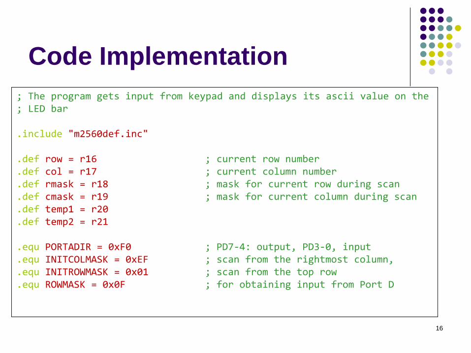
Code Implementation
; The program gets input from keypad and displays its ascii value on the; LED bar
.include "m2560def.inc"
.def row = r16 ; current row number
.def col = r17 ; current column number
.def rmask = r18 ; mask for current row during scan
.def cmask = r19 ; mask for current column during scan
.def temp1 = r20
.def temp2 = r21
.equ PORTADIR = 0xF0 ; PD7-4: output, PD3-0, input
.equ INITCOLMASK = 0xEF ; scan from the rightmost column,
.equ INITROWMASK = 0x01 ; scan from the top row
.equ ROWMASK = 0x0F ; for obtaining input from Port D
17
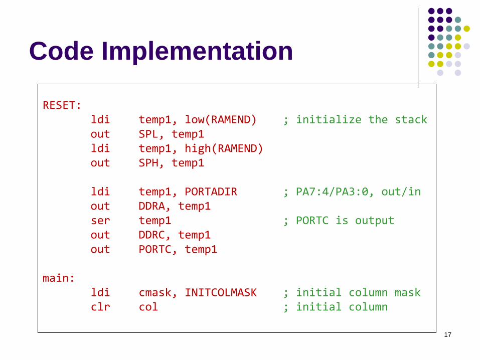
Code Implementation
RESET:ldi temp1, low(RAMEND) ; initialize the stackout SPL, temp1ldi temp1, high(RAMEND)out SPH, temp1
ldi temp1, PORTADIR ; PA7:4/PA3:0, out/inout DDRA, temp1ser temp1 ; PORTC is outputout DDRC, temp1out PORTC, temp1
main:ldi cmask, INITCOLMASK ; initial column maskclr col ; initial column
18
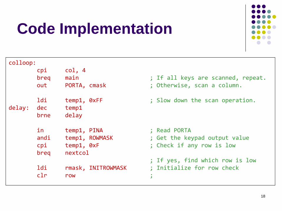
Code Implementation
colloop:cpi col, 4breq main ; If all keys are scanned, repeat.out PORTA, cmask ; Otherwise, scan a column.
ldi temp1, 0xFF ; Slow down the scan operation.delay: dec temp1
brne delay
in temp1, PINA ; Read PORTAandi temp1, ROWMASK ; Get the keypad output valuecpi temp1, 0xF ; Check if any row is lowbreq nextcol
; If yes, find which row is lowldi rmask, INITROWMASK ; Initialize for row checkclr row ;
19
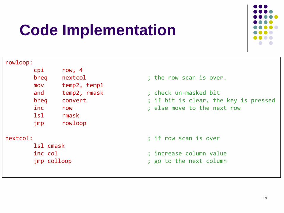
Code Implementation
rowloop:cpi row, 4breq nextcol ; the row scan is over.mov temp2, temp1and temp2, rmask ; check un-masked bitbreq convert ; if bit is clear, the key is pressedinc row ; else move to the next rowlsl rmaskjmp rowloop
nextcol: ; if row scan is overlsl cmaskinc col ; increase column valuejmp colloop ; go to the next column
20
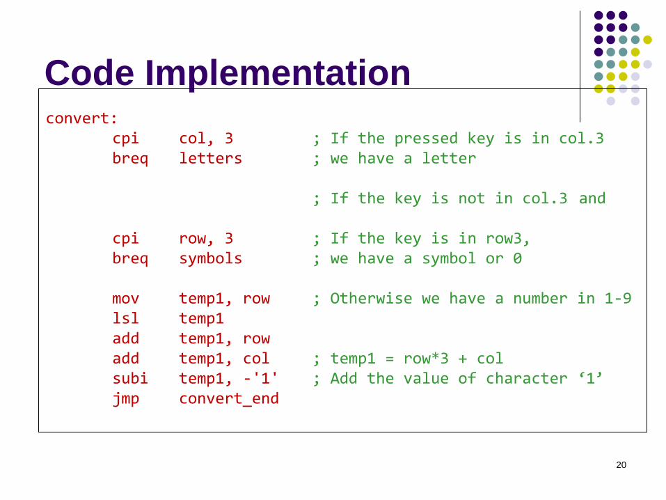
Code Implementationconvert:
cpi col, 3 ; If the pressed key is in col.3 breq letters ; we have a letter
; If the key is not in col.3 and
cpi row, 3 ; If the key is in row3,breq symbols ; we have a symbol or 0
mov temp1, row ; Otherwise we have a number in 1-9lsl temp1add temp1, rowadd temp1, col ; temp1 = row*3 + colsubi temp1, -'1' ; Add the value of character ‘1’jmp convert_end
21
Code Implementation
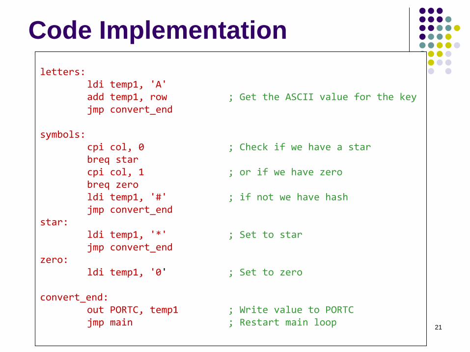
letters:ldi temp1, 'A'add temp1, row ; Get the ASCII value for the keyjmp convert_end
symbols:cpi col, 0 ; Check if we have a starbreq starcpi col, 1 ; or if we have zerobreq zeroldi temp1, '#' ; if not we have hashjmp convert_end
star:ldi temp1, '*' ; Set to starjmp convert_end
zero:ldi temp1, '0' ; Set to zero
convert_end:out PORTC, temp1 ; Write value to PORTCjmp main ; Restart main loop
22
LCD
⚫ Liquid Crystal Display
⚫ Programmable output device
23
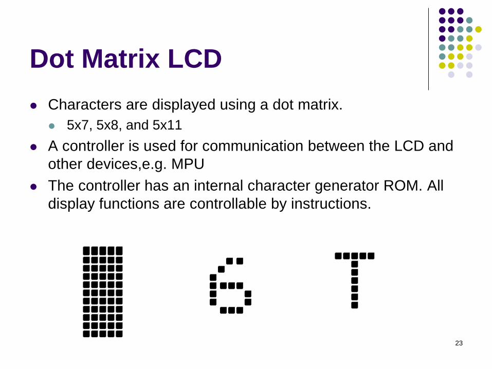
Dot Matrix LCD
⚫ Characters are displayed using a dot matrix.
⚫ 5x7, 5x8, and 5x11
⚫ A controller is used for communication between the LCD and
other devices,e.g. MPU
⚫ The controller has an internal character generator ROM. All
display functions are controllable by instructions.
24
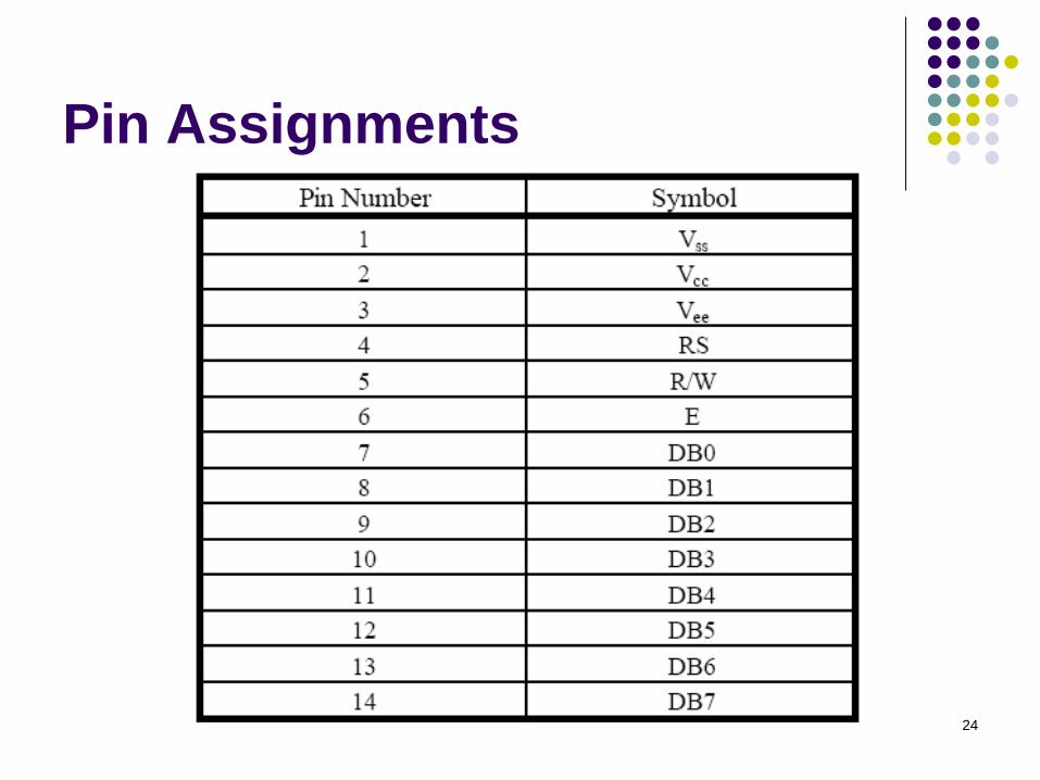
Pin Assignments
25
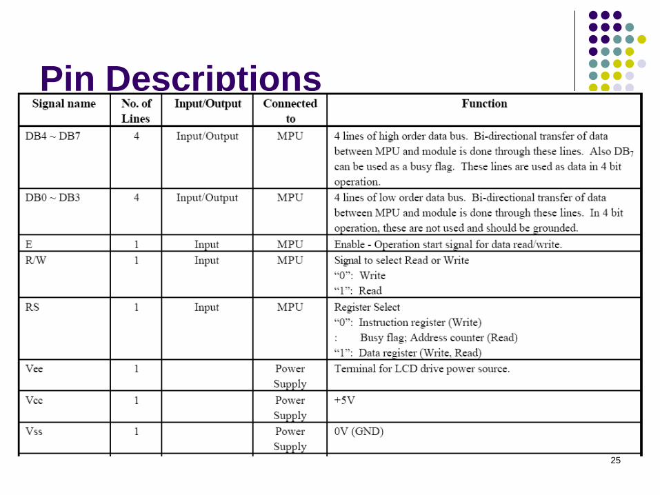
Pin Descriptions
26
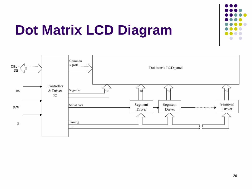
Dot Matrix LCD Diagram
27
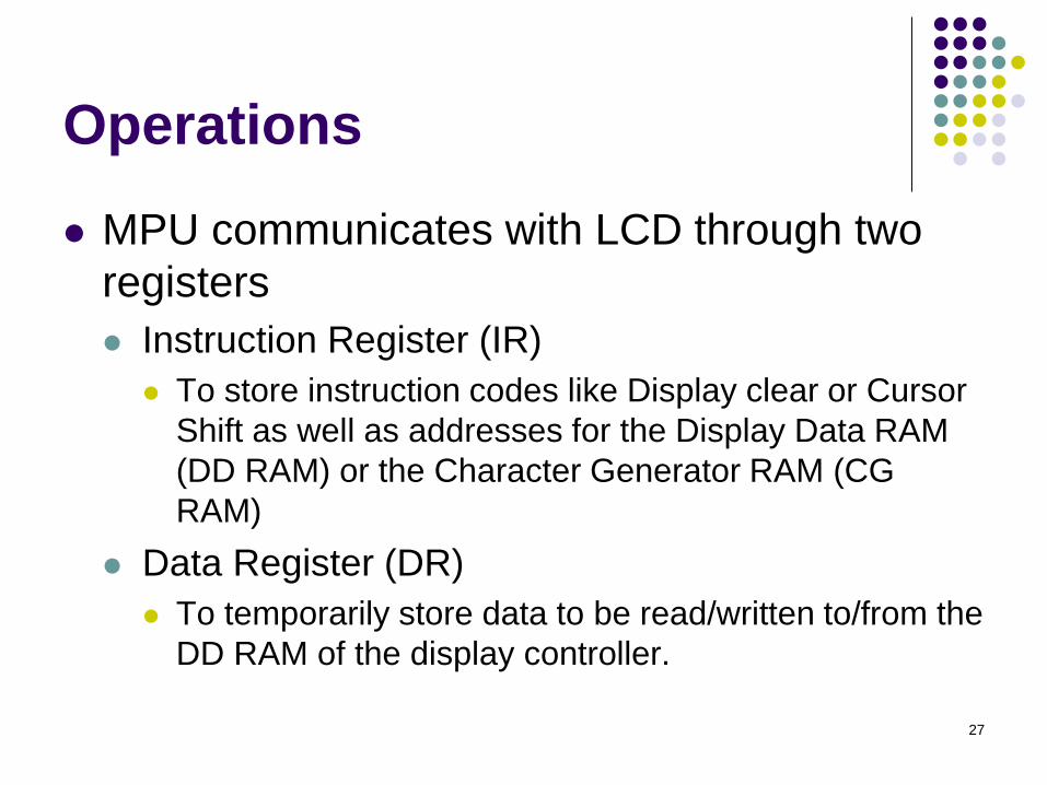
Operations
⚫ MPU communicates with LCD through two
registers
⚫ Instruction Register (IR)
⚫ To store instruction codes like Display clear or Cursor
Shift as well as addresses for the Display Data RAM
(DD RAM) or the Character Generator RAM (CG
RAM)
⚫ Data Register (DR)
⚫ To temporarily store data to be read/written to/from the
DD RAM of the display controller.
28
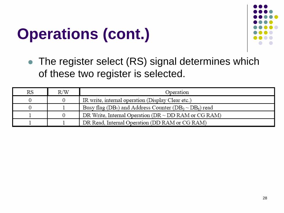
Operations (cont.)
⚫ The register select (RS) signal determines which
of these two register is selected.
29
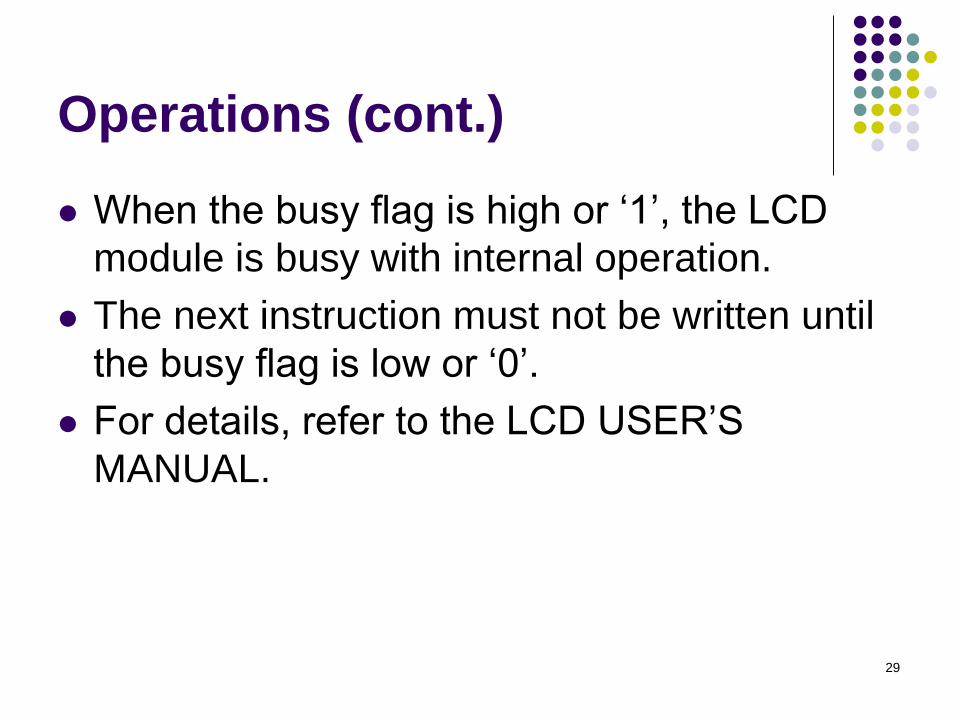
Operations (cont.)
⚫ When the busy flag is high or ‘1’, the LCD
module is busy with internal operation.
⚫ The next instruction must not be written until
the busy flag is low or ‘0’.
⚫ For details, refer to the LCD USER’S
MANUAL.
30
LCD Instructions
⚫ A list of binary instructions are available for
LCD operations
⚫ Some typical ones are explained in the next
slides.
31
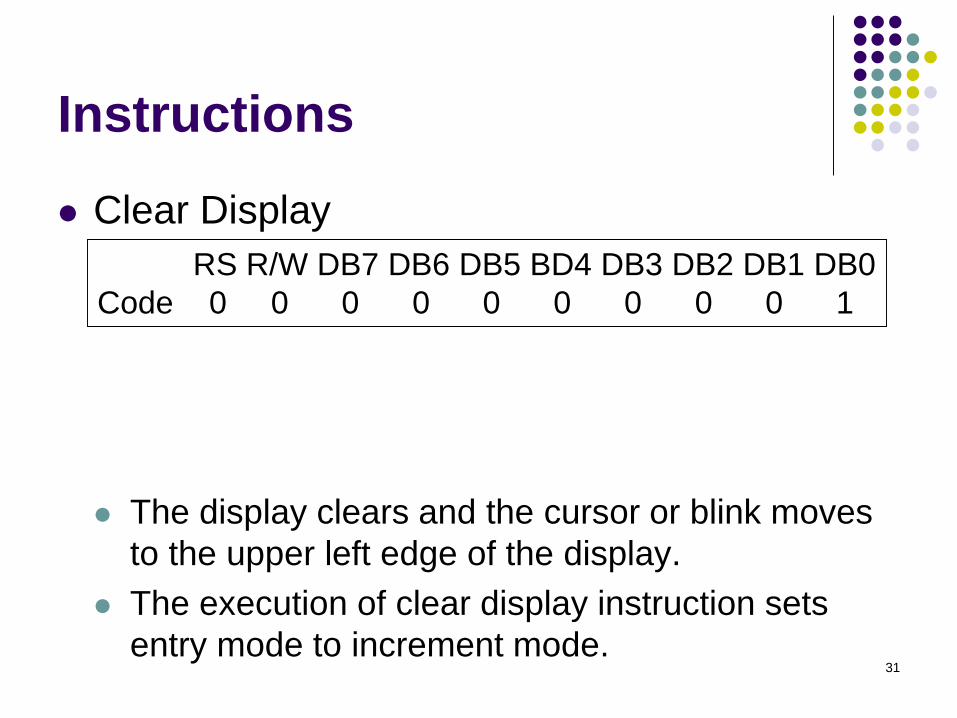
Instructions
⚫ Clear Display
⚫ The display clears and the cursor or blink moves
to the upper left edge of the display.
⚫ The execution of clear display instruction sets
entry mode to increment mode.
RS R/W DB7 DB6 DB5 BD4 DB3 DB2 DB1 DB0
Code 0 0 0 0 0 0 0 0 0 1
32
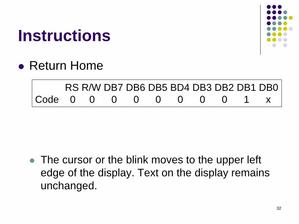
Instructions
⚫ Return Home
⚫ The cursor or the blink moves to the upper left
edge of the display. Text on the display remains
unchanged.
RS R/W DB7 DB6 DB5 BD4 DB3 DB2 DB1 DB0
Code 0 0 0 0 0 0 0 0 1 x
33
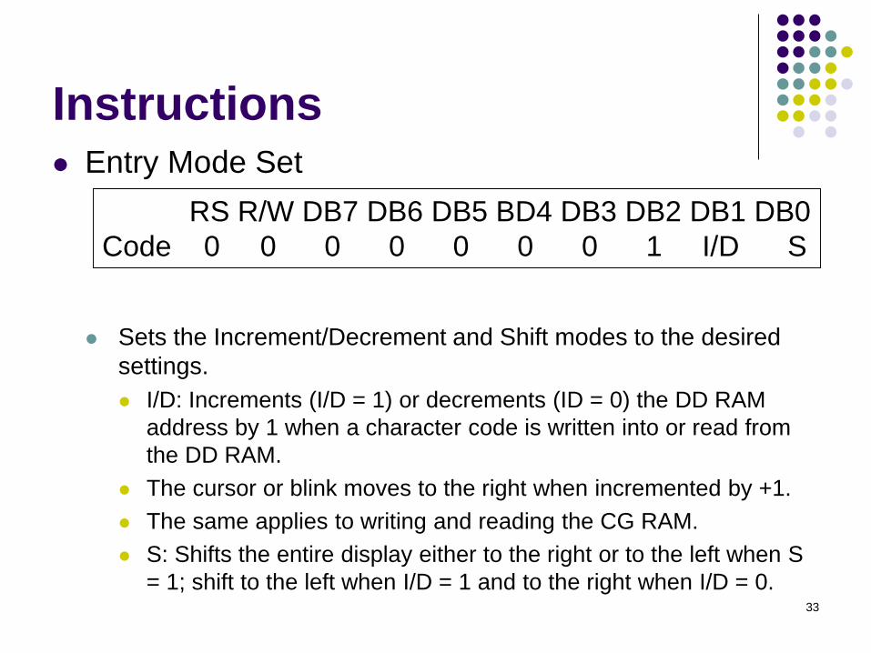
Instructions⚫ Entry Mode Set
⚫ Sets the Increment/Decrement and Shift modes to the desired
settings.
⚫ I/D: Increments (I/D = 1) or decrements (ID = 0) the DD RAM
address by 1 when a character code is written into or read from
the DD RAM.
⚫ The cursor or blink moves to the right when incremented by +1.
⚫ The same applies to writing and reading the CG RAM.
⚫ S: Shifts the entire display either to the right or to the left when S
= 1; shift to the left when I/D = 1 and to the right when I/D = 0.
RS R/W DB7 DB6 DB5 BD4 DB3 DB2 DB1 DB0
Code 0 0 0 0 0 0 0 1 I/D S
34
Instructions
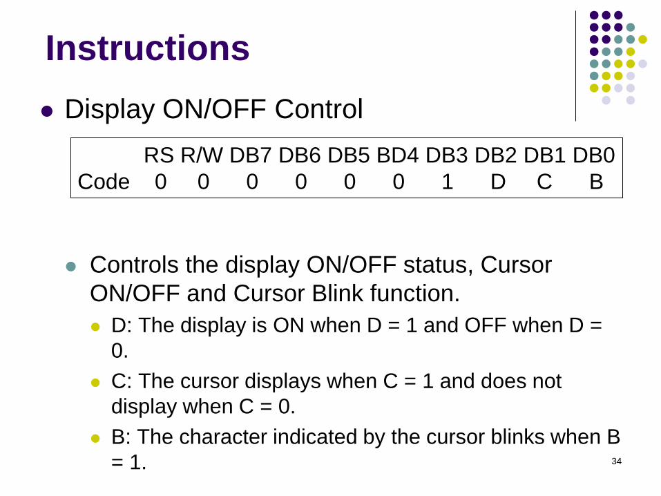
⚫ Display ON/OFF Control
⚫ Controls the display ON/OFF status, Cursor
ON/OFF and Cursor Blink function.
⚫ D: The display is ON when D = 1 and OFF when D =
0.
⚫ C: The cursor displays when C = 1 and does not
display when C = 0.
⚫ B: The character indicated by the cursor blinks when B
= 1.
RS R/W DB7 DB6 DB5 BD4 DB3 DB2 DB1 DB0
Code 0 0 0 0 0 0 1 D C B
35
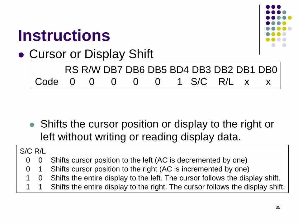
Instructions⚫ Cursor or Display Shift
⚫ Shifts the cursor position or display to the right or
left without writing or reading display data.
RS R/W DB7 DB6 DB5 BD4 DB3 DB2 DB1 DB0
Code 0 0 0 0 0 1 S/C R/L x x
S/C R/L
0 0 Shifts cursor position to the left (AC is decremented by one)
0 1 Shifts cursor position to the right (AC is incremented by one)
1 0 Shifts the entire display to the left. The cursor follows the display shift.
1 1 Shifts the entire display to the right. The cursor follows the display shift.
36
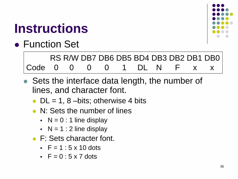
Instructions⚫ Function Set
⚫ Sets the interface data length, the number of lines, and character font.
⚫ DL = 1, 8 –bits; otherwise 4 bits
⚫ N: Sets the number of lines
▪ N = 0 : 1 line display
▪ N = 1 : 2 line display
⚫ F: Sets character font.
▪ F = 1 : 5 x 10 dots
▪ F = 0 : 5 x 7 dots
RS R/W DB7 DB6 DB5 BD4 DB3 DB2 DB1 DB0
Code 0 0 0 0 1 DL N F x x
37
Instructions
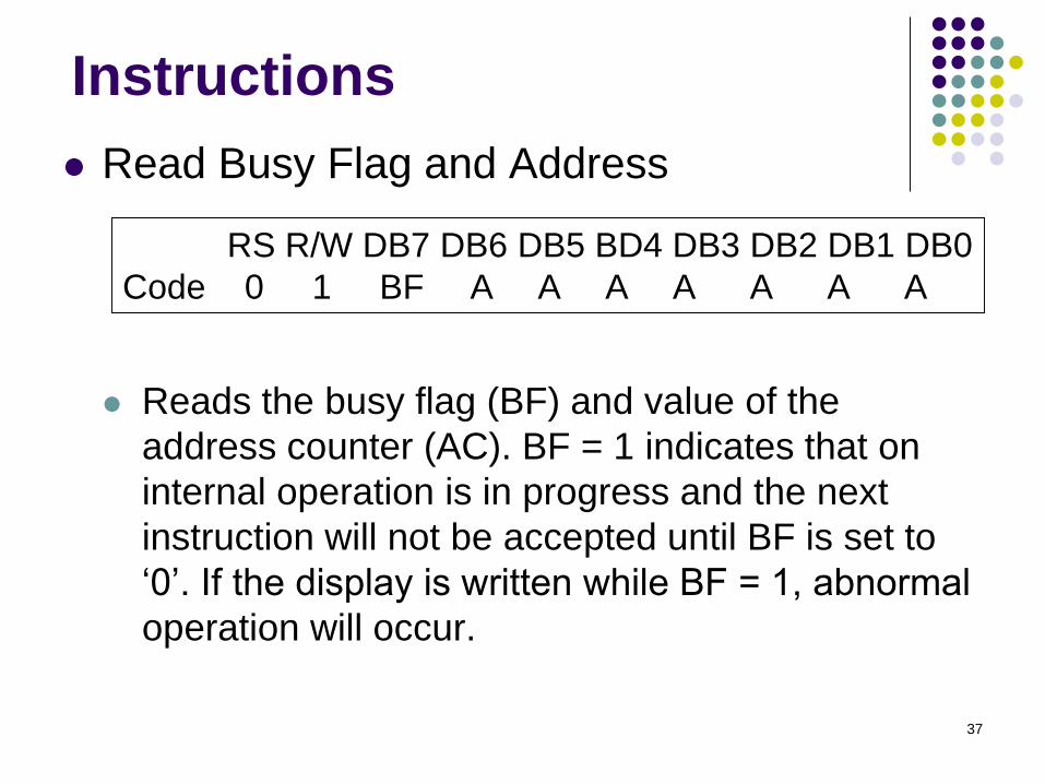
⚫ Read Busy Flag and Address
⚫ Reads the busy flag (BF) and value of the
address counter (AC). BF = 1 indicates that on
internal operation is in progress and the next
instruction will not be accepted until BF is set to
‘0’. If the display is written while BF = 1, abnormal
operation will occur.
RS R/W DB7 DB6 DB5 BD4 DB3 DB2 DB1 DB0
Code 0 1 BF A A A A A A A
38
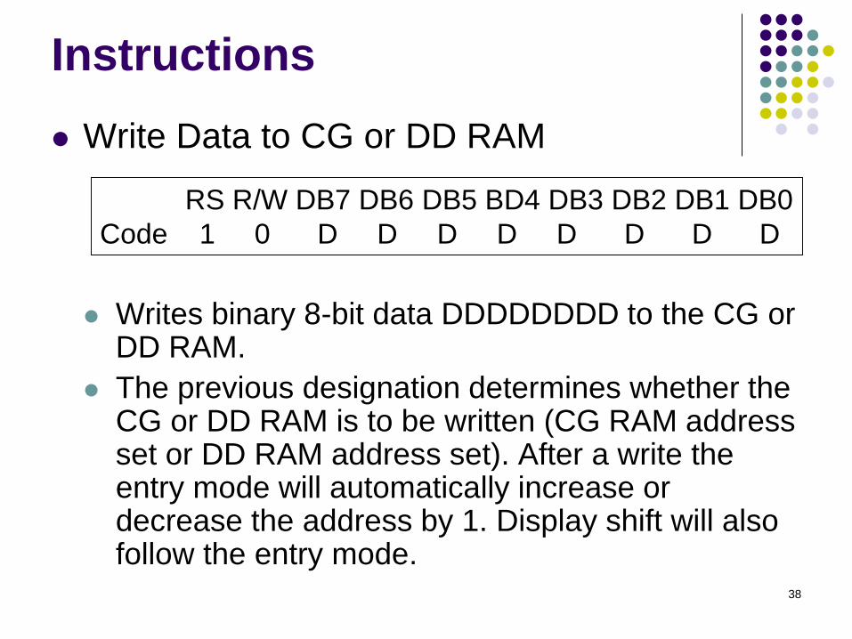
Instructions
⚫ Write Data to CG or DD RAM
⚫ Writes binary 8-bit data DDDDDDDD to the CG or DD RAM.
⚫ The previous designation determines whether the CG or DD RAM is to be written (CG RAM address set or DD RAM address set). After a write the entry mode will automatically increase or decrease the address by 1. Display shift will also follow the entry mode.
RS R/W DB7 DB6 DB5 BD4 DB3 DB2 DB1 DB0
Code 1 0 D D D D D D D D
39
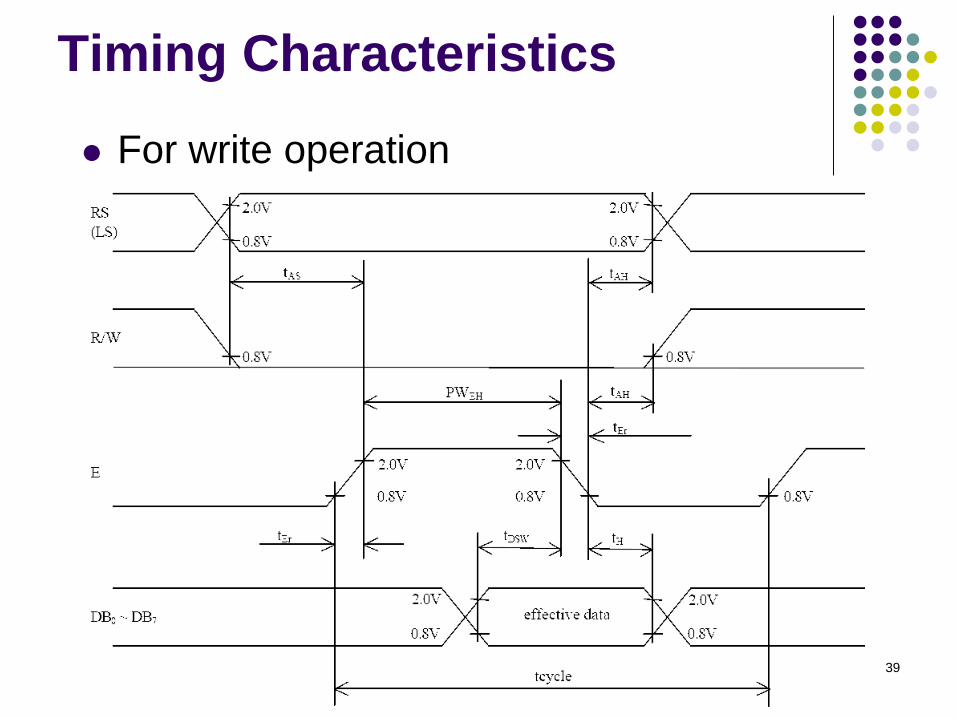
Timing Characteristics
⚫ For write operation
40
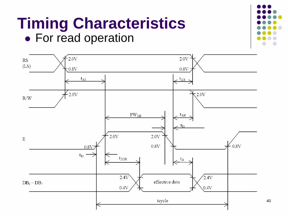
Timing Characteristics⚫ For read operation
41
Examples
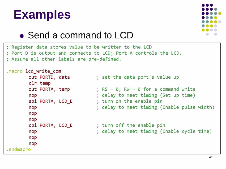
⚫ Send a command to LCD; Register data stores value to be written to the LCD; Port D is output and connects to LCD; Port A controls the LCD.; Assume all other labels are pre-defined.
.macro lcd_write_comout PORTD, data ; set the data port's value upclr tempout PORTA, temp ; RS = 0, RW = 0 for a command writenop ; delay to meet timing (Set up time)sbi PORTA, LCD_E ; turn on the enable pinnop ; delay to meet timing (Enable pulse width)nopnopcbi PORTA, LCD_E ; turn off the enable pinnop ; delay to meet timing (Enable cycle time)nopnop
.endmacro
42
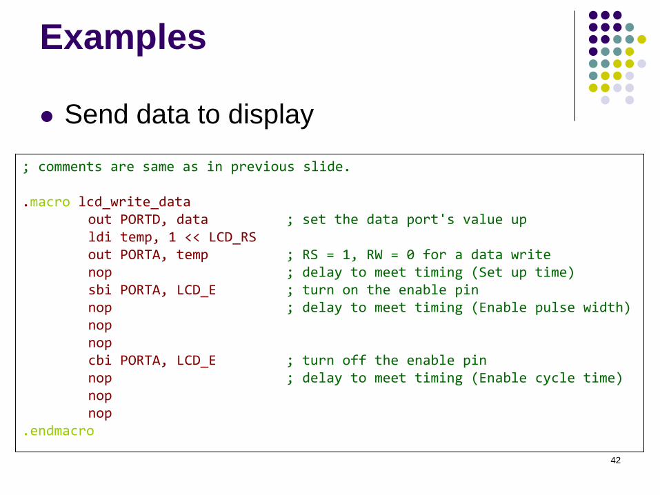
Examples
⚫ Send data to display
; comments are same as in previous slide.
.macro lcd_write_dataout PORTD, data ; set the data port's value upldi temp, 1 << LCD_RSout PORTA, temp ; RS = 1, RW = 0 for a data writenop ; delay to meet timing (Set up time)sbi PORTA, LCD_E ; turn on the enable pinnop ; delay to meet timing (Enable pulse width)nopnopcbi PORTA, LCD_E ; turn off the enable pinnop ; delay to meet timing (Enable cycle time)nopnop
.endmacro
43
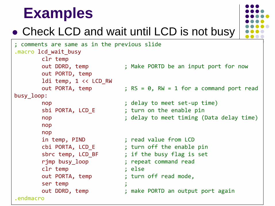
Examples⚫ Check LCD and wait until LCD is not busy; comments are same as in the previous slide .macro lcd_wait_busy
clr tempout DDRD, temp ; Make PORTD be an input port for nowout PORTD, templdi temp, 1 << LCD_RWout PORTA, temp ; RS = 0, RW = 1 for a command port read
busy_loop:nop ; delay to meet set-up time)sbi PORTA, LCD_E ; turn on the enable pinnop ; delay to meet timing (Data delay time)nopnopin temp, PIND ; read value from LCDcbi PORTA, LCD_E ; turn off the enable pinsbrc temp, LCD_BF ; if the busy flag is setrjmp busy_loop ; repeat command readclr temp ; elseout PORTA, temp ; turn off read mode,ser temp ; out DDRD, temp ; make PORTD an output port again
.endmacro
44
LCD Initialization
⚫ LCD should be initialized before use
⚫ Internal Reset Circuit can be used, but it is
related to power supply loading, may not
work properly.
⚫ Therefore, software initialization is
recommended.
45
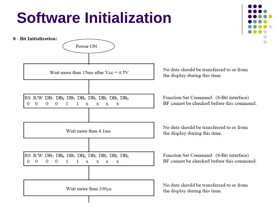
Software Initialization
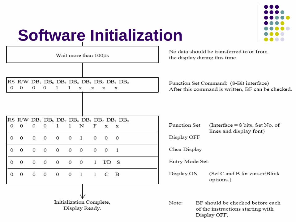
46
Software Initialization
47
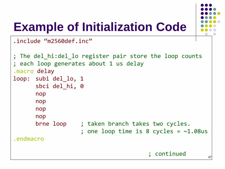
Example of Initialization Code.include “m2560def.inc”
; The del_hi:del_lo register pair store the loop counts; each loop generates about 1 us delay.macro delayloop: subi del_lo, 1
sbci del_hi, 0nopnopnopnopbrne loop ; taken branch takes two cycles.
; one loop time is 8 cycles = ~1.08us.endmacro
; continued
48
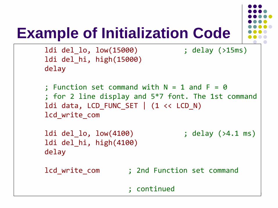
Example of Initialization Codeldi del_lo, low(15000) ; delay (>15ms)ldi del_hi, high(15000)delay
; Function set command with N = 1 and F = 0; for 2 line display and 5*7 font. The 1st commandldi data, LCD_FUNC_SET | (1 << LCD_N) lcd_write_com
ldi del_lo, low(4100) ; delay (>4.1 ms)ldi del_hi, high(4100)delay
lcd_write_com ; 2nd Function set command
; continued
49
Example of Initialization Code
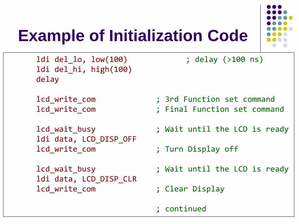
ldi del_lo, low(100) ; delay (>100 ns)ldi del_hi, high(100)delay
lcd_write_com ; 3rd Function set commandlcd_write_com ; Final Function set command
lcd_wait_busy ; Wait until the LCD is readyldi data, LCD_DISP_OFFlcd_write_com ; Turn Display off
lcd_wait_busy ; Wait until the LCD is readyldi data, LCD_DISP_CLRlcd_write_com ; Clear Display
; continued
50
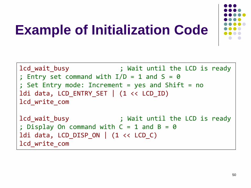
Example of Initialization Code
lcd_wait_busy ; Wait until the LCD is ready; Entry set command with I/D = 1 and S = 0; Set Entry mode: Increment = yes and Shift = noldi data, LCD_ENTRY_SET | (1 << LCD_ID) lcd_write_com
lcd_wait_busy ; Wait until the LCD is ready; Display On command with C = 1 and B = 0ldi data, LCD_DISP_ON | (1 << LCD_C)lcd_write_com
51
Reading Material
⚫ Chapter 7: Computer Buses and Parallel
Input and Output. Microcontrollers and
Microcomputers by Fredrick M. Cady.
⚫ Simple I/O Devices
⚫ DOT Matrix LCD User’s Manual
⚫ Available on the course website.
52
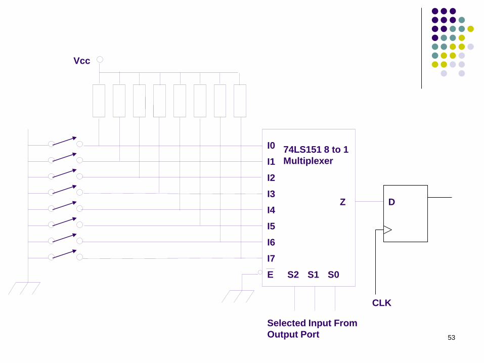
Homework
1. The circuit shown in the next slide is a
switch array input circuit. Is there any switch
bounce issue with this circuit? Can the CLK
frequency have any impact on this problem?
How to solve it in hardware?
53
I0
I2
I3
I4
I5
I6
I7
I1
E S2 S1 S0
Selected Input From
Output Port
Z
74LS151 8 to 1
Multiplexer
Vcc
D
CLK
54
Homework
2. Write an assembly program to initialize LCD
panel to display characters in one line with
5x7 font.