Embed Size (px)
Citation preview
Inkjet Printing—Process and Its Applications
By Madhusudan Singh, Hanna M. Haverinen, Parul Dhagat, andGhassan E. Jabbour*
1. Introduction
The organic electronics roadmap identifies organic and printedelectronics market to exceed $300 billion over the next 20 years.[1]
Print technology borrowed from the graphic arts and newspaperindustry can be adapted in principle to the production of largevolume organic electronics. In particular, digital inkjet printing,which has been used as a low cost research tool, is facilitatinginitial explorations of various aspects of printed electronics in alaboratory setting. The appeal of this technology lies in it being anon-contact, additive patterning and maskless approach. Directwrite attribute of inkjet printing allows for deposition of versatilethin films, the designs of which can be changed with ease frombatch to batch. Other attractive features of this technology are:reduced material wastage, low cost, and scalability to large areamanufacturing.
In the sections that follow, we will attempt to present a briefoverview of recent progress in the understanding of inkjetprinting process (Section 2). A section on progress in organicthin-film transistors (Section 3) will be followed by a review ofprinted light-emitting devices (LEDs, Section 4). The develop-ment of economically viable solar cells requires high throughput
processes, and inkjet printing provides anideal capability for initial process develop-ment (Section 5). This will be followed by asummary of recent developments in print-ing of magnetic nanoparticles (Section 6)for memory and other related applications.All devices, organic thin film transistors(OTFTs), LEDs, and solar cells, requirecontactsandconductivestructures (Section7)as part of larger circuits that integrate them.
Sensors and detectors are an integral part of many aspects ofmodern life, such as light detectors, safety, and securityapplications such as toxic gas sensors, etc. Many of theseapplications require inexpensive, often single-use devices that areideally suited to inkjet printing. We will present a discussion ofnotable reports of progress in this field (Section 8). Finally, we willmake a very brief survey of progress in printed biological andpharmaceutical devices and applications (Section 9), and the useof inkjet printing as a patterning process (Section 10), concludingwith a concise summary. This Progress Report is not intended tobe exhaustive in nature, but we choose particular applications ofinkjet printing, which in our opinion, offer the greatest advancein their respective fields in recent years, and most promise forforthcoming work of a significant nature.
2. Inkjet Printing Process
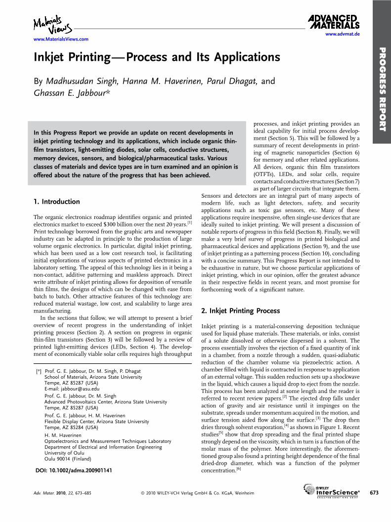
Inkjet printing is a material-conserving deposition techniqueused for liquid phase materials. These materials, or inks, consistof a solute dissolved or otherwise dispersed in a solvent. Theprocess essentially involves the ejection of a fixed quantity of inkin a chamber, from a nozzle through a sudden, quasi-adiabaticreduction of the chamber volume via piezoelectric action. Achamber filled with liquid is contracted in response to applicationof an external voltage. This sudden reduction sets up a shockwavein the liquid, which causes a liquid drop to eject from the nozzle.This process has been analyzed at some length and the reader isreferred to recent review papers.[2] The ejected drop falls underaction of gravity and air resistance until it impinges on thesubstrate, spreads undermomentum acquired in themotion, andsurface tension aided flow along the surface.[3] The drop thendries through solvent evaporation,[4] as shown in Figure 1. Recentstudies[5] show that drop spreading and the final printed shapestrongly depend on the viscosity, which in turn is a function of themolar mass of the polymer. More interestingly, the aforemen-tioned group also found a printing height dependence of the finaldried-drop diameter, which was a function of the polymerconcentration.[6]
PROGRESS
REPORT
www.MaterialsViews.comwww.advmat.de
[*] Prof. G. E. Jabbour, Dr. M. Singh, P. DhagatSchool of Materials, Arizona State UniversityTempe, AZ 85287 (USA)E-mail: [email protected]
Prof. G. E. Jabbour, Dr. M. SinghAdvanced Photovoltaics Center, Arizona State UniversityTempe, AZ 85287 (USA)
Prof. G. E. Jabbour, H. M. HaverinenFlexible Display Center, Arizona State UniversityTempe, AZ 85284 (USA)
H. M. HaverinenOptoelectronics and Measurement Techniques LaboratoryDepartment of Electrical and Information EngineeringUniversity of OuluOulu 90014 (Finland)
DOI: 10.1002/adma.200901141
In this Progress Report we provide an update on recent developments ininkjet printing technology and its applications, which include organic thin-film transistors, light-emitting diodes, solar cells, conductive structures,memory devices, sensors, and biological/pharmaceutical tasks. Variousclasses of materials and device types are in turn examined and an opinion isoffered about the nature of the progress that has been achieved.
Adv. Mater. 2010, 22, 673–685 ! 2010 WILEY-VCH Verlag GmbH & Co. KGaA, Weinheim 673

PROGRESS
REPORT
www.advmat.dewww.MaterialsViews.com
Most conventional understanding of the inkjet printingprocess depends on assuming the flow of the fluid ink as aNewtonian fluid. This assumption is often invalid, especially inthe case of the ‘‘rebound’’ of a fluid upon impact on a printingsubstrate with low surface energy. Bartolo et al. developed anunderstanding of the interaction of a non-Newtonian fluid withthe substrate as a function of normal stress at the contact linebetween the fluid and the substrate.[7] They demonstrated thatthe rebound of the drop can be controlled or even preventedthrough addition of a small amount of flexible polymer to thesolvent.
The flow properties of dilute polymer solutions are ofimmediate interest for the development of inkjet printingprocesses. Measurements such as contact angle presented by asingle drop on the substrate of interest, coupled with ameasurement of the viscosity, surface tension, and computationalfluid dynamics modeling using software such as Fluent (ANSYS),have been used to study the flow process as well as interaction of afalling drop with the substrate. However, such an approach isnecessarily approximate as it lacks direct measurements of fluidflow patterns, which can be critical for printing applications. Hillet al.[8] have introduced a rheofluorescent technique for the studyof fluorescent polymers in a shear field. The method involves theinvestigation of dependence of fluorescence from poly[2-methoxy-5-(20-ethyl-hexyloxy)-(1,4-phenylene vinylene)] (MEH-PPV) in a Couette flow situation between two cylinders, whichrotate relatively to generate a shear force. Rheochromism, whichinvolves a shift in the fluorescence peak depending on the appliedshear force in a fluid, is studied to infer changes in segmentlength in the conjugated polymer. Polymer segment length,which is directly related to the molecular weight and, hence,viscosity, has a critical impact on the flow properties inpiezoelectric inkjet printing, a situation that does involvecompression of the fluid and shearing prior to its ejection fromthe nozzle. While this technique does not offer a direct handle onthe actual flow pattern, it permits the study of the relationshipbetween the optimal shear stress and the molecular weight of thespecies being printed.
Direct imaging offers a more direct measurement of ink flowpatterns. The development of such a technique has been reportedby Dong et al.[9] Here, a drop-on-demand (DOD) piezoelectricinkjet printing systemwas used in conjunction with a pulsed laserand a flash photography setup to obtain sufficient brightness inthe field of view as well as good time resolution for direct imagingmeasurements of the drops. Several fluids, including DI water,glycerin-based mixtures of water, and isopropyl alcohol were usedto measure the processes of ejection and stretching of fluid,necking and pinch-off of liquid streaks from nozzle, recoil of thefreely falling liquid streak, breakup of the streak, formation andbreakup of primary drop and satellites, stretching of the liquiddrop, etc. The authors developed criteria for avoiding theformation of satellite drops that are responsible for reduction ofresolution in the printing process. A less sophisticated method ofreliably measuring the dried-drop size, which affects themorphology of the final print, involves the use of silicananoparticles[10] in order to map the spreading of the drop andrelate dried-drop size to the size of the sessile drop.
Inkjet printing depends critically on the behavior of ejectedprinted drops after the jetting action. These falling drops are
affected by several factors including jetting conditions andproperties of the ambient. Tsai et al.[11] studied the effects of pulsevoltage on droplet breakup time from the nozzle, dropletmorphology, drop velocity, and droplet size of silver nanoparticlesdispersed in DI water, using pure DI water as control. They foundthat: (i) more viscous ink had a higher onset bias and created alonger liquid column and small droplets; (ii) by applyingintermediate bias to both inks, two droplets were generatedafter jetting but they recombined before hitting the surface;(iii) higher voltages resulted in separated droplets that neverrecombined; (iv) break-off time is independent of the pulse bias;and (v) the pinch-off point for both solutions was different, wheresilver powder suspensions had lower pinch-off point compared tothose of bare DI water.
In most cases, fabrication of functional device structures withinkjet printing involves the use of prepatterned substrates atmultiple levels of processing, and potentially (in many cases)involving multiple materials. Such situations result in morecomplicated fluid flow patterns when compared to the simplecase of a printed drop impinging on a flat substrate. Modeling ofinteraction of printed drop with a prepatterned surface has beentreated by Khatavkar et al.[12] The authors used a diffuse interfacemodel to consider the effect of wettability of the barrier and widthof the barrier. Not surprisingly, the results indicated that forconstant barrier geometry, wettability of the barrier is critical todetermination of spreading of the printed drop.
Printing of thin lines is limited by the size of the drop, whichdepends ultimately on jetting conditions, the ink, surface energyof substrate, and nozzle diameter. Intuitively, the nozzle diametershould form the fundamental lower bound on the drop size,barring any unusual jetting conditions. Machining of smallernozzles in inkjet cartridges is possible but it involves morecomplicated processes, thereby increasing cost. Further, smallernozzles are easier to clog, thereby reducing the reliability andrepeatability of the jetting process. Hence, the development of aprinting process that can produce features smaller than thenozzle diameter is desirable. Such a process has beendemonstrated by Goghari and Chandra[13] for water–glycerin
Ghassan E. Jabbour is thedirector of the AdvancedPhotovoltaics Center atArizona State University (ASU),a director of researchoptoelectronic materials anddevices at the Flexible DisplayCenter (FDC), and a Professorof the School of Materials atASU. He attended NorthernArizona University, MIT, andUniversity of Arizona. He
received his bachelor’s degrees in Physics, ElectricalEngineering, and Materials Science and Engineering. Prof.Jabbour is a SPIE fellow and a Distinguished Prof. of Finland,Academy of Finland. His research interests are flexible andstretchable electronic materials, energy, nanoelectronics,and photonics.
674 ! 2010 WILEY-VCH Verlag GmbH & Co. KGaA, Weinheim Adv. Mater. 2010, 22, 673–685
PROGRESS
REPORT
www.MaterialsViews.comwww.advmat.de
mixtures with intermediate concentrations. They developed acustom drop generator that exploits fluid instability to form smalldroplets. This instability depends on the material parameterssatisfying certain conditions. The authors found that theOhnesorge number,
Oh ! m!!!!!!!!rds
p (1)
where m, r, and s are the viscosity, density, and surface tension ofthe ink, while d is the nozzle diameter, is a good predictor of whensuch conditions are satisfied.
At high integration densities, such as for electrophoreticbackplanes, the tolerances online non-uniformities can be verytight. Thus, it is desirable to directly control the nature of theinteraction between the ink and substrate. The coffee-ring effect,for instance, arises in part from interaction of multiple effects ofdrying of the solvent, resultant changes in the viscosity of the ink,transport of the solute via motion of the solvent, the latter motionarising from surface tension interaction between the solvent andthe substrate, etc. It would be advantageous to arrest the finalgeometry and layout of ink drops on the substrate in a very shortperiod of time after deposition. Use of thermally gelatingpolymers is one method that can help ensure this outcome.Printing of continuous polymer lines using gelating polymers hasbeen demonstrated by van den Berg et al.[14] The authors used adiblock copolymer poly(vinyl methyl ether)-block-poly(vinyloxy-4-butyric acid) colloidally stabilizing a TiO2 ink. Thermallygelating materials exhibit strong temperature dependence. Theauthors found a temperature-dependent increase in ink viscosity,which increased dramatically above 37 8C, along with thecorresponding increase in print fidelity for printed drops andlines.
Other methods to increase resolution of printed featuresinvolve bypassing thermal/acoustic printing altogether and useelectric fields to drive the printing process. An electrohydrody-namic jetting (EHJ) technique to achieve sub-micrometerresolutions was developed by Park et al.[15] resulting in featuresizes in the range of 240 nm to 5mm. The reader is referred to thispaper for more details on printing processes that involve the useof very high electric fields to propel ink drops, forming a Taylorcone at the tip of the capillary. An application of this approach tobiological systems will be presented in Section 9.
Polymers and other solutions and suspen-sions lend themselves readily to inkjet print-ing. Fabrication of structures that involvespecies other than polymers or small mole-cules/macromolecules that are easily dissolvedin solvents presents a new set of challenges.For instance, suspensions of metal nanopar-ticles tend to be unstable in ordinary solventsand can require complicated chemical mod-ifications that involve use of stabilizers.Printed nanoparticles behave differently fromprinted polymers and other solutions owing totheir higher specific gravity and increasedlikelihood for phase separation. The finalassembly of such nanoparticles on the sub-
strate depends on surface treatments which change surfaceenergy properties. Perelaer et al.[10] investigated packing of inkjetprinted spherical silica nanoparticles. The study involved fourdifferent nanoparticle sizes stabilized with hydroxyl or silanolsurface groups in a 1wt % aqueous solution. Using differentsurface treatments, the authors found that larger particles packedcloser to the center of the droplet when the contact angle washigh, while smaller particles under the same conditions migratedcloser to the contact line at the edge of the droplet. Furthermore,the use of highly hydrophobic substrates assisted in packing ofnanoparticles, avoiding coffee-ring formation.
Inkjet printing of homogenous polymer solutions is common.However, the use of colloidal suspensions expands the repertoireof polymer/solvent combinations that can be printed. This abilityis particularly vital in designing a pure inkjet printing-basedprocess to fabricate multiple layers with orthogonal solvents.Printing of aqueous inks containing a 40wt % polyurethanesuspension in water was demonstrated by van den Berg et al.[16]
Using white light interferometry, the authors found that use ofhigher solute contents reduces print non-uniformities that arisefrom the coffee-ring effect.[3] The height of the single dropdeposited was found to be 3mm, while printing of a completelayer revealed a thickness of 10mm. The authors also attempted toprint a step structure resulting in a pyramid with a height of87mm.
We have thus attempted to address the gamut of features andissues unique to the inkjet printing process. These involve themeasurement of rheological properties of the inks, droplet–substrate interactions, post-jetting behavior of printed droplets inflight and after collision with the substrate. We have brieflysurveyed recent work on methods used to enhance the resolutionof device structures composed of polymers and metallicnanoparticles. We now turn to various applications of inkjetprinting.
3. Thin-Film Transistors
A key active element for implementing organic circuits is theOTFT. Use of OTFTs has been demonstrated in low-endapplications, which do not require significantly high mobilityand switching speeds, such as RFID tags[17] and displaybackplanes.[18] We will now discuss significant accomplishmentsin the area of printed organic transistors. We will focus on bothall-printed and hybrid devices (where conventional lithography is
Figure 1. The process of drop drying after deposition with inkjet printing. Reproduced withpermission from [4]. Copyright 2008, Wiley-VCH.
Adv. Mater. 2010, 22, 673–685 ! 2010 WILEY-VCH Verlag GmbH & Co. KGaA, Weinheim 675
PROGRESS
REPORT
www.advmat.dewww.MaterialsViews.com
used in conjunction with printing). An OTFT is a four-layer devicewith two layers of electrode material (source, drain, and the gate)and one layer each of dielectric and active organic material.Although the basic structure of an OTFT appears simple,complexity arises due to registration and solvent orthogonalityissues with layer-by-layer printing. These problems can becompounded when printing on nonplanar substrates, as the casefor flexible electronics. Additionally, the switching speed of acircuit depends upon mobility and the channel length (L) tochannel width (W) ratio of the transistor. In most cases, inkjetprinting offers a resolution "20mm,[1] but limits the smallestchannel length that can be achieved. This has implications on thecircuit design, limiting the switching speeds to 1–100Hz.[19]
Most of the recent efforts have been focused on reducing thechannel length in order to overcome the switching speedlimitation. Sirringhaus et al.[20] successfully demonstrated the useof a hybrid approach to create channel lengths from themicrometer to sub-100 nm range. They used lithographicallypatterned hydrophobic polyimide banks to contain the spread ofinkjet printed source–drain (S/D) electrodes on a hydrophilicglass substrate[20] creating channel features with #5mmseparation. Further reduction in the channel lengths was possibleusing e-beam lithography to pattern a hydrophobic self-assembled monolayer (SAM) mesa-like structure, which variedin width from 20mm to 250 nm. Surface energy differencesbetween the mesa and the substrate split an inkjet-printed dropletinto two separate S/D electrodes with the length of the channelbeing defined by the width of the SAM mesa.[21] Furthermore,they demonstrated the use of nanoimprint lithography to createtrenches in polymethyl methacrylate (PMMA) with a separationof 250 nm (which defined the channel length) in order to confineprinted droplets.[22] For devices mentioned above, poly(3,4-ethylenedioxythiophene):poly(styrenesulfonate) (PEDOT:PSS)was used as the S/D electrode material. The organic semi-conductor and the dielectric material were spin-coated, and finallythe gate electrode (PEDOT:PSS) was printed on top of thedielectric layer with a registration accuracy of 1mm, to completethe device.
However, the use of conventional lithography tools is expectedto lead to an increase in production cost. A more cost-effectiveapproach based upon self-aligning electrodes, resulting in100 nm channel lengths, was developed.[23] This techniquerequires inkjet printing first set of PEDOT:PSS electrodes andtreating them with a carbon tetrafluoride (CF4) plasma to create ahydrophobic surface. Next, a second set of PEDOT:PSS electrodesare printed partially overlapping the first set. Ink from the secondprint is repelled from the first set of electrodes, before drying inthe vicinity forming a sub-100 nm self-aligned gap (SAG) betweenthe two electrodes. Additive printing of organic semiconductorand gate electrode complete the device, with solvent being theonly material wasted. Use of this approach resulted in transistorswith mobility values of 0.002 cm2 V$1 s$1 with poly(9,9-dioctylfluorene-co-bithiophene) (F8T2), a liquid crystalline poly-mer. The authors also demonstrated that addition of a surfactantto the PEDOT:PSS ink also created a self-aligned separationbetween printed electrodes. The hydrophilic tail groups from thesurfactant accumulate on the surface of the drying droplet due tosegregation of the surfactant to the surface. This creates alow-surface tension layer surrounding the droplet, which repels
the second printed droplet. More recently, they were able to acombine the SAG with a high mobility organic semiconductorpoly(2,5-bis(3-dodecylthiophene-2-yl)thieno[3,2-b]thiophene) (pBTTT)to obtain respectable mobility values of 0.1–0.2 cm2 V$1 s$1.However, in this case, printed gold electrodes (s! 104 S cm$1)treated with a hydrophobic SAM were used to repel the secondprinted electrode to resulting in channel lengths from 60nm to4mm. Inverters based on these transistors exhibited frequenciesas high as 1.6MHz.[19]
In order to fabricate all-printed OTFTs, the dielectrics have to becompatible with the inkjet processing of subsequent layers.Orthogonal solvents are required in order to prevent dissolution oflayers that have been previously printed. Despite the difficulties inensuring these conditions, all-printed transistors have been demon-strated using pentacene precursors and poly-4-vinylphenol (PVP)dielectric;[24] and polypyrrole and PVP-K60.[25] Additive printing ofactive layer inks (organic semiconductors dissolved in varioussolvents) such as poly[5,50-bis(3-dodecyl-2-thienyl)-2, 20-bithiophene](PQT-12),[26] F8T2,[27] air-stable poly(3-hexylthiophene) (P3HT)derivatives,[28] 6,13-bis(triisopropylsilylethynyl) pentacene (TIPspentacene),[29] other pentacene precursors and oligothophenes[30]
have been demonstrated. Recently, carbon nanotubes (mobili-ty# 0.07 cm2V$1 s$1) have been inkjet printed as the activematerialforOTFTs.[31]Other inorganic species suchaspolysilicon[32] andzincoxide nanoparticles[33] have also been successfully inkjet-printed asactive layers in a transistor. Electrodematerials such asPEDOT:PSS,silvernanoparticle inks,goldandcoppernanoparticle inkshavebeenutilized as potential candidates.[28,34–37]
Next, we focus on using inkjet printing as a digital lithographytool in order to create masks such that the minimum printablefeature size defines the channel length of the device. The PARCgroup has demonstrated the use of wax as a photoresist tolithographically define S/D electrodes pattern on blanket metalthin films.[27,38] Areas that are covered by the wax are protectedfromsubsequent lithographic processes such asmetal etching andphotoresist removal. The drop size is controlled by temperature ofboth wax and substrate, resulting in channel lengths ranging from40 to400mm.Digital lithographyusingwaxhasbeenused todefineall the three electrodes in a coplanar bottom gate OTFTs and hasbeen successfully used to create backplanes for electrophoreticdisplays using PQT-12 as the active material. This resulted inmobility values of 0.06–0.2 cm2 V$1 s$1 for channel lengths of30–50mm.[26] The same group demonstrated similar performancewith a printed backplane[39] consisting of silver nanoparticle lineswith a resistivity of 5% 10$6V cm.We will address the printing ofsuch conductive structures at greater length in Section 7. Printedwax has not only been used to define critical devices features butalso used for selective patterning process.[40] On a substrate withpredefined S/D electrodes, the channel region is covered with waxafterwhich the substrate is exposed to SAMmaking the uncoveredarea hydrophobic. The wax is then removed exposing thehydrophilic region underneath it. The substrate is dipped in anorganic polymer solution and gradually removed to allow forselective dewetting of the solution from the hydrophobic regionsonto the hydrophilic areas. This simple patterning of organicsemiconductor layer offers good registration between successivelayers.
The accurate placement of the active material within the gateelectrode region prevents large leakage currents and crosstalk
676 ! 2010 WILEY-VCH Verlag GmbH & Co. KGaA, Weinheim Adv. Mater. 2010, 22, 673–685
PROGRESS
REPORT
www.MaterialsViews.comwww.advmat.de
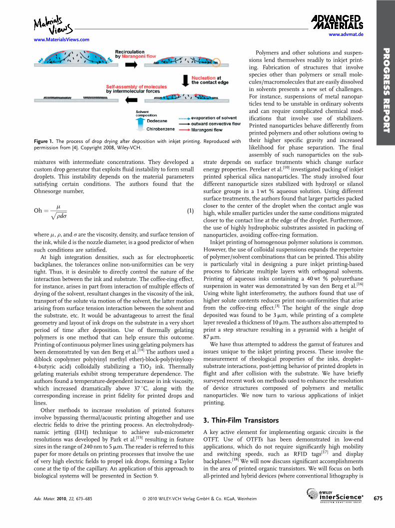
between TFT pixels, as well as conserves ink.Recently, Lim et al.[4] demonstrated use ofsolvent mixtures to balance the Marangoni andconvective flows in a drying droplet, therebycontrolling morphology of the dried droplet(Fig. 2). The evaporation rate is controlledusing a high surface tension and high boilingpoint solvent (major solvent) mixed with alower boiling point solvent (minor solvent) andsurface tension less than that of the majorcomponent. A convective flow is establishedfrom the center toward the drying edge of thedroplet as the evaporation rate is faster at theperiphery; driven by the surface tensiongradient between the edge of the drop andthe center. However, this surface tensiongradient creates an opposing Marangoni flow,which results in recirculation of the solventin the droplet. The dried droplet then resultedin large self organized crystals of TIPspentacene which provided mobility as highas 0.12 cm2 V$1 s$1.
Inkjet printing of OTFTs has been limited tobottom contact architecture wherein theelectrodes were S/D electrodes were depositedbefore the organic active layer. This preventeddamage to the organic active layer from the inksolvent, preserving the device performance.Also, the registration issues were limited to theprinting of gate electrode for top gate. Recently,there have been developments with top contactOTFT geometry, where the metal S/D electro-des are printed on top of the active layer.[41,42]
Ability to control the drop volume to picoliter values, limited theamount of organic solvent dispensed on top of the active layer.Another advantage of reduced droplet volume was a decrease insintering temperature for metallic nanoparticles that formed theelectrodes preventing subsequent damage to the underlyingorganic layer. Continuous metallic lines as narrow as 1mm withresistivity values of #25mV cm were obtained in this manner.Further details of this report will be presented in Section 7.Mobility obtained for pentacene OTFTs fabricated using printedelectrodes was 0.1–0.3 cm2 V$1 s$1, which is comparable withthose of evaporated electrodes. This technique was alsodemonstrated on an n-type semiconductor copper hexadeca-fluorophthalocyanine (F16CuPc) resulting in mobility values of0.02 cm2 V$1 s$1 (L! 5mm). This also benefits the bottomcontact geometry where much smaller feature sizes can beobtained without the use of conventional lithographic processesfor miniaturization of printed circuits.
High integration densities of field-effect transistors (FETs) andTFTs require device structures with a high capacitance per unitarea to maintain proper control of the channel. Perovskites likeBaTiO3
[43] and polar materials like LiNbO3[44] can be used to
enhance such control through enhancement of capacitance perunit area, in addition to more exotic polar effects such as chargeinduction. It is thus desirable to develop an inkjet printingtechnique for deposition of such materials accurately over thechannel. Tseng et al.[45] demonstrated the deposition of BaTiO3-Ni
perovskite films through inkjet printing. The authors printed60-nm-diameter BaTiO3 nanoparticles, and 90-nm-diametermetallic nickel particles with purity >99% on flexible porousacetate sheets using a propylene glycol-based surfactant todisperse the nanoparticles in ethanol–isopropanol solvent blend.
However, before the commercialization of TFT and FET-basedproducts, there are road blocks that require immediate attentionand significant amount of work. Registration of features atdifferent layers of print has to be resolved for high throughputinkjet printing. The solvents need to be compatible when printingsubsequent layers and yet be environmentally safe for use in largescale production. Additionally, passivation of the printed device isalso important for long lifetime operation capabilities. Recently,Arias et al.[46] have demonstrated the feasibility of using blendedactive and encapsulation material that phase separate uponprinting in the channel region. There is limited exposure of theactive polymer to ambient conditions during the print cycle andresulted in cost effective printing of both active and encapsulationlayer in a single step.
4. Light-Emitting Devices
Inkjet printing does not require the use of shadowmasks as it is adirect writing process. This property of inkjet printing makes it asuitable technique for combinatorial studies[47,48] of various
Figure 2. Optical microscopy and polarized images of the inkjet-printed droplets of TIPSpentacene using chlorobenzene as the major solvent mixed with 25% of the minor solvent,a) chlorobenzene, b) hexane, c) o-dichlorobenzene, and d) dodecane. (Scale bar represents50mm) The profilometery images of single dots using chlorobenzene mixed with 25% minorsolvents, e) chlorobenzene, f) hexane, g) o-dichlorobenzene are also shown. Reproduced withpermission from [4]. Copyright 2008, Wiley-VCH.
Adv. Mater. 2010, 22, 673–685 ! 2010 WILEY-VCH Verlag GmbH & Co. KGaA, Weinheim 677
PROGRESS
REPORT
www.advmat.dewww.MaterialsViews.com
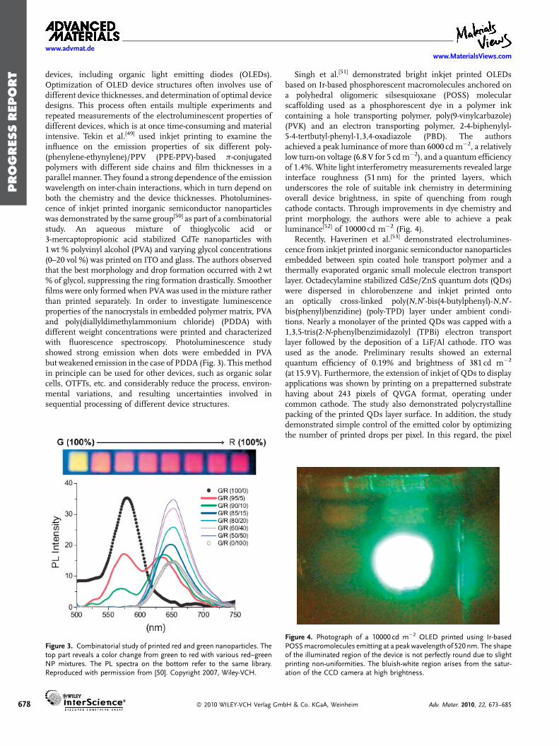
devices, including organic light emitting diodes (OLEDs).Optimization of OLED device structures often involves use ofdifferent device thicknesses, and determination of optimal devicedesigns. This process often entails multiple experiments andrepeated measurements of the electroluminescent properties ofdifferent devices, which is at once time-consuming and materialintensive. Tekin et al.[49] used inkjet printing to examine theinfluence on the emission properties of six different poly-(phenylene-ethynylene)/PPV (PPE-PPV)-based p-conjugatedpolymers with different side chains and film thicknesses in aparallel manner. They found a strong dependence of the emissionwavelength on inter-chain interactions, which in turn depend onboth the chemistry and the device thicknesses. Photolumines-cence of inkjet printed inorganic semiconductor nanoparticleswas demonstrated by the same group[50] as part of a combinatorialstudy. An aqueous mixture of thioglycolic acid or3-mercaptopropionic acid stabilized CdTe nanoparticles with1wt % polyvinyl alcohol (PVA) and varying glycol concentrations(0–20 vol %) was printed on ITO and glass. The authors observedthat the best morphology and drop formation occurred with 2wt% of glycol, suppressing the ring formation drastically. Smootherfilms were only formed when PVAwas used in the mixture ratherthan printed separately. In order to investigate luminescenceproperties of the nanocrystals in embedded polymer matrix, PVAand poly(diallyldimethylammonium chloride) (PDDA) withdifferent weight concentrations were printed and characterizedwith fluorescence spectroscopy. Photoluminescence studyshowed strong emission when dots were embedded in PVAbut weakened emission in the case of PDDA (Fig. 3). Thismethodin principle can be used for other devices, such as organic solarcells, OTFTs, etc. and considerably reduce the process, environ-mental variations, and resulting uncertainties involved insequential processing of different device structures.
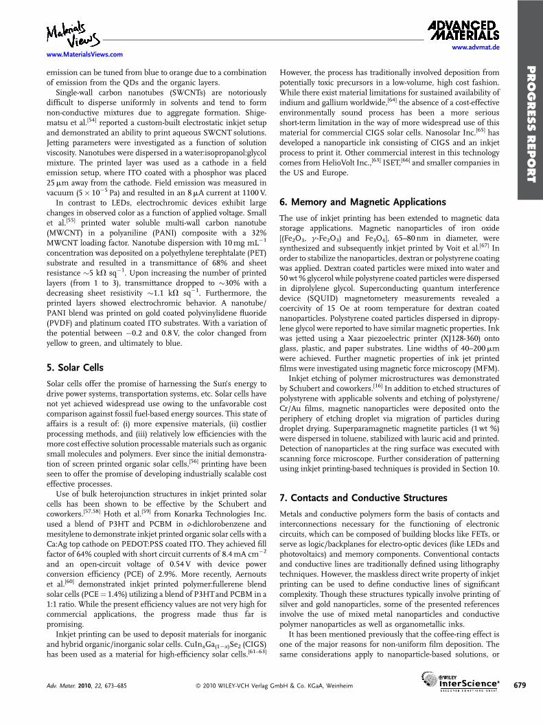
Singh et al.[51] demonstrated bright inkjet printed OLEDsbased on Ir-based phosphorescent macromolecules anchored ona polyhedral oligomeric silsesquioxane (POSS) molecularscaffolding used as a phosphorescent dye in a polymer inkcontaining a hole transporting polymer, poly(9-vinylcarbazole)(PVK) and an electron transporting polymer, 2-4-biphenylyl-5-4-tertbutyl-phenyl-1,3,4-oxadiazole (PBD). The authorsachieved a peak luminance of more than 6000 cd m$2, a relativelylow turn-on voltage (6.8 V for 5 cdm$2), and a quantum efficiencyof 1.4%. White light interferometry measurements revealed largeinterface roughness (51 nm) for the printed layers, whichunderscores the role of suitable ink chemistry in determiningoverall device brightness, in spite of quenching from roughcathode contacts. Through improvements in dye chemistry andprint morphology, the authors were able to achieve a peakluminance[52] of 10000 cd m$2 (Fig. 4).
Recently, Haverinen et al.[53] demonstrated electrolumines-cence from inkjet printed inorganic semiconductor nanoparticlesembedded between spin coated hole transport polymer and athermally evaporated organic small molecule electron transportlayer. Octadecylamine stabilized CdSe/ZnS quantum dots (QDs)were dispersed in chlorobenzene and inkjet printed ontoan optically cross-linked poly(N,N0-bis(4-butylphenyl)-N,N0-bis(phenyl)benzidine) (poly-TPD) layer under ambient condi-tions. Nearly a monolayer of the printed QDs was capped with a1,3,5-tris(2-N-phenylbenzimidazolyl (TPBi) electron transportlayer followed by the deposition of a LiF/Al cathode. ITO wasused as the anode. Preliminary results showed an externalquantum efficiency of 0.19% and brightness of 381 cd m$2
(at 15.9 V). Furthermore, the extension of inkjet of QDs to displayapplications was shown by printing on a prepatterned substratehaving about 243 pixels of QVGA format, operating undercommon cathode. The study also demonstrated polycrystallinepacking of the printed QDs layer surface. In addition, the studydemonstrated simple control of the emitted color by optimizingthe number of printed drops per pixel. In this regard, the pixel
Figure 3. Combinatorial study of printed red and green nanoparticles. Thetop part reveals a color change from green to red with various red–greenNP mixtures. The PL spectra on the bottom refer to the same library.Reproduced with permission from [50]. Copyright 2007, Wiley-VCH.
Figure 4. Photograph of a 10000 cd m$2 OLED printed using Ir-basedPOSSmacromolecules emitting at a peak wavelength of 520 nm. The shapeof the illuminated region of the device is not perfectly round due to slightprinting non-uniformities. The bluish-white region arises from the satur-ation of the CCD camera at high brightness.
678 ! 2010 WILEY-VCH Verlag GmbH & Co. KGaA, Weinheim Adv. Mater. 2010, 22, 673–685
PROGRESS
REPORT
www.MaterialsViews.comwww.advmat.de
emission can be tuned from blue to orange due to a combinationof emission from the QDs and the organic layers.
Single-wall carbon nanotubes (SWCNTs) are notoriouslydifficult to disperse uniformly in solvents and tend to formnon-conductive mixtures due to aggregate formation. Shige-matsu et al.[54] reported a custom-built electrostatic inkjet setupand demonstrated an ability to print aqueous SWCNT solutions.Jetting parameters were investigated as a function of solutionviscosity. Nanotubes were dispersed in a water:isopropanol:glycolmixture. The printed layer was used as a cathode in a fieldemission setup, where ITO coated with a phosphor was placed25mm away from the cathode. Field emission was measured invacuum (5% 10$5 Pa) and resulted in an 8mA current at 1100V.
In contrast to LEDs, electrochromic devices exhibit largechanges in observed color as a function of applied voltage. Smallet al.[55] printed water soluble multi-wall carbon nanotube(MWCNT) in a polyaniline (PANI) composite with a 32%MWCNT loading factor. Nanotube dispersion with 10mg mL$1
concentration was deposited on a polyethylene terephtalate (PET)substrate and resulted in a transmittance of 68% and sheetresistance #5 kV sq$1. Upon increasing the number of printedlayers (from 1 to 3), transmittance dropped to #30% with adecreasing sheet resistivity #1.1 kV sq$1. Furthermore, theprinted layers showed electrochromic behavior. A nanotube/PANI blend was printed on gold coated polyvinylidene fluoride(PVDF) and platinum coated ITO substrates. With a variation ofthe potential between $0.2 and 0.8 V, the color changed fromyellow to green, and ultimately to blue.
5. Solar Cells
Solar cells offer the promise of harnessing the Sun’s energy todrive power systems, transportation systems, etc. Solar cells havenot yet achieved widespread use owing to the unfavorable costcomparison against fossil fuel-based energy sources. This state ofaffairs is a result of: (i) more expensive materials, (ii) costlierprocessing methods, and (iii) relatively low efficiencies with themore cost effective solution processable materials such as organicsmall molecules and polymers. Ever since the initial demonstra-tion of screen printed organic solar cells,[56] printing have beenseen to offer the promise of developing industrially scalable costeffective processes.
Use of bulk heterojunction structures in inkjet printed solarcells has been shown to be effective by the Schubert andcoworkers.[57,58] Hoth et al.[59] from Konarka Technologies Inc.used a blend of P3HT and PCBM in o-dichlorobenzene andmesitylene to demonstrate inkjet printed organic solar cells with aCa:Ag top cathode on PEDOT:PSS coated ITO. They achieved fillfactor of 64% coupled with short circuit currents of 8.4mA cm$2
and an open-circuit voltage of 0.54V with device powerconversion efficiency (PCE) of 2.9%. More recently, Aernoutset al.[60] demonstrated inkjet printed polymer:fullerene blendsolar cells (PCE! 1.4%) utilizing a blend of P3HTand PCBM in a1:1 ratio. While the present efficiency values are not very high forcommercial applications, the progress made thus far ispromising.
Inkjet printing can be used to deposit materials for inorganicand hybrid organic/inorganic solar cells. CuInxGa(1$x)Se2 (CIGS)has been used as a material for high-efficiency solar cells.[61–63]
However, the process has traditionally involved deposition frompotentially toxic precursors in a low-volume, high cost fashion.While there exist material limitations for sustained availability ofindium and gallium worldwide,[64] the absence of a cost-effectiveenvironmentally sound process has been a more seriousshort-term limitation in the way of more widespread use of thismaterial for commercial CIGS solar cells. Nanosolar Inc.[65] hasdeveloped a nanoparticle ink consisting of CIGS and an inkjetprocess to print it. Other commercial interest in this technologycomes fromHelioVolt Inc.,[63] ISET,[66] and smaller companies inthe US and Europe.
6. Memory and Magnetic Applications
The use of inkjet printing has been extended to magnetic datastorage applications. Magnetic nanoparticles of iron oxide[(Fe2O3, g -Fe2O3) and Fe3O4], 65–80 nm in diameter, weresynthesized and subsequently inkjet printed by Voit et al.[67] Inorder to stabilize the nanoparticles, dextran or polystyrene coatingwas applied. Dextran coated particles were mixed into water and50wt % glycerol while polystyrene coated particles were dispersedin diprolylene glycol. Superconducting quantum interferencedevice (SQUID) magnetometery measurements revealed acoercivity of 15 Oe at room temperature for dextran coatednanoparticles. Polystyrene coated particles dispersed in dipropy-lene glycol were reported to have similar magnetic properties. Inkwas jetted using a Xaar piezoelectric printer (XJ128-360) ontoglass, plastic, and paper substrates. Line widths of 40–200mmwere achieved. Further magnetic properties of ink jet printedfilms were investigated using magnetic force microscopy (MFM).
Inkjet etching of polymer microstructures was demonstratedby Schubert and coworkers.[16] In addition to etched structures ofpolystyrene with applicable solvents and etching of polystyrene/Cr/Au films, magnetic nanoparticles were deposited onto theperiphery of etching droplet via migration of particles duringdroplet drying. Superparamagnetic magnetite particles (1wt %)were dispersed in toluene, stabilized with lauric acid and printed.Detection of nanoparticles at the ring surface was executed withscanning force microscope. Further consideration of patterningusing inkjet printing-based techniques is provided in Section 10.
7. Contacts and Conductive Structures
Metals and conductive polymers form the basis of contacts andinterconnections necessary for the functioning of electroniccircuits, which can be composed of building blocks like FETs, orserve as logic/backplanes for electro-optic devices (like LEDs andphotovoltaics) and memory components. Conventional contactsand conductive lines are traditionally defined using lithographytechniques. However, the maskless direct write property of inkjetprinting can be used to define conductive lines of significantcomplexity. Though these structures typically involve printing ofsilver and gold nanoparticles, some of the presented referencesinvolve the use of mixed metal nanoparticles and conductivepolymer nanoparticles as well as organometallic inks.
It has been mentioned previously that the coffee-ring effect isone of the major reasons for non-uniform film deposition. Thesame considerations apply to nanoparticle-based solutions, or
Adv. Mater. 2010, 22, 673–685 ! 2010 WILEY-VCH Verlag GmbH & Co. KGaA, Weinheim 679
PROGRESS
REPORT
www.advmat.dewww.MaterialsViews.com
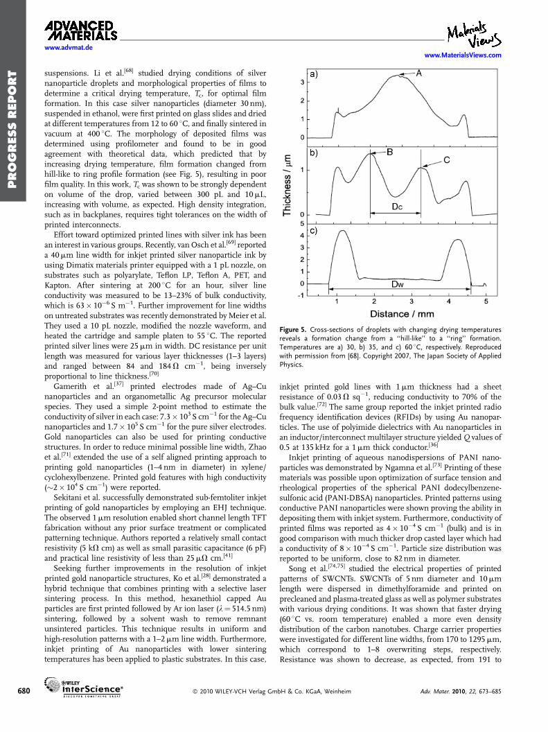
suspensions. Li et al.[68] studied drying conditions of silvernanoparticle droplets and morphological properties of films todetermine a critical drying temperature, Tc, for optimal filmformation. In this case silver nanoparticles (diameter 30 nm),suspended in ethanol, were first printed on glass slides and driedat different temperatures from 12 to 60 8C, and finally sintered invacuum at 400 8C. The morphology of deposited films wasdetermined using profilometer and found to be in goodagreement with theoretical data, which predicted that byincreasing drying temperature, film formation changed fromhill-like to ring profile formation (see Fig. 5), resulting in poorfilm quality. In this work, Tc was shown to be strongly dependenton volume of the drop, varied between 300 pL and 10mL,increasing with volume, as expected. High density integration,such as in backplanes, requires tight tolerances on the width ofprinted interconnects.
Effort toward optimized printed lines with silver ink has beenan interest in various groups. Recently, van Osch et al.[69] reporteda 40mm line width for inkjet printed silver nanoparticle ink byusing Dimatix materials printer equipped with a 1 pL nozzle, onsubstrates such as polyarylate, Teflon LP, Teflon A, PET, andKapton. After sintering at 200 8C for an hour, silver lineconductivity was measured to be 13–23% of bulk conductivity,which is 63% 10$6 S m$1. Further improvement for line widthson untreated substrates was recently demonstrated by Meier et al.They used a 10 pL nozzle, modified the nozzle waveform, andheated the cartridge and sample platen to 55 8C. The reportedprinted silver lines were 25mm in width. DC resistance per unitlength was measured for various layer thicknesses (1–3 layers)and ranged between 84 and 184V cm$1, being inverselyproportional to line thickness.[70]
Gamerith et al.[37] printed electrodes made of Ag–Cunanoparticles and an organometallic Ag precursor molecularspecies. They used a simple 2-point method to estimate theconductivity of silver in each case: 7.3% 103 S cm$1 for the Ag–Cunanoparticles and 1.7% 105 S cm$1 for the pure silver electrodes.Gold nanoparticles can also be used for printing conductivestructures. In order to reduce minimal possible line width, Zhaoet al.[71] extended the use of a self aligned printing approach toprinting gold nanoparticles (1–4 nm in diameter) in xylene/cyclohexylbenzene. Printed gold features with high conductivity(#2% 104 S cm$1) were reported.
Sekitani et al. successfully demonstrated sub-femtoliter inkjetprinting of gold nanoparticles by employing an EHJ technique.The observed 1mm resolution enabled short channel length TFTfabrication without any prior surface treatment or complicatedpatterning technique. Authors reported a relatively small contactresistivity (5 kV cm) as well as small parasitic capacitance (6 pF)and practical line resistivity of less than 25mV cm.[41]
Seeking further improvements in the resolution of inkjetprinted gold nanoparticle structures, Ko et al.[28] demonstrated ahybrid technique that combines printing with a selective lasersintering process. In this method, hexanethiol capped Auparticles are first printed followed by Ar ion laser (l! 514.5 nm)sintering, followed by a solvent wash to remove remnantunsintered particles. This technique results in uniform andhigh-resolution patterns with a 1–2mm line width. Furthermore,inkjet printing of Au nanoparticles with lower sinteringtemperatures has been applied to plastic substrates. In this case,
inkjet printed gold lines with 1mm thickness had a sheetresistance of 0.03V sq$1, reducing conductivity to 70% of thebulk value.[72] The same group reported the inkjet printed radiofrequency identification devices (RFIDs) by using Au nanopar-ticles. The use of polyimide dielectrics with Au nanoparticles inan inductor/interconnect multilayer structure yielded Q values of0.5 at 135 kHz for a 1mm thick conductor.[36]
Inkjet printing of aqueous nanodispersions of PANI nano-particles was demonstrated by Ngamna et al.[73] Printing of thesematerials was possible upon optimization of surface tension andrheological properties of the spherical PANI dodecylbenzene-sulfonic acid (PANI-DBSA) nanoparticles. Printed patterns usingconductive PANI nanoparticles were shown proving the ability indepositing them with inkjet system. Furthermore, conductivity ofprinted films was reported as 4% 10$4 S cm$1 (bulk) and is ingood comparison with much thicker drop casted layer which hada conductivity of 8% 10$4 S cm$1. Particle size distribution wasreported to be uniform, close to 82 nm in diameter.
Song et al.[74,75] studied the electrical properties of printedpatterns of SWCNTs. SWCNTs of 5 nm diameter and 10mmlength were dispersed in dimethylforamide and printed onprecleaned and plasma-treated glass as well as polymer substrateswith various drying conditions. It was shown that faster drying(60 8C vs. room temperature) enabled a more even densitydistribution of the carbon nanotubes. Charge carrier propertieswere investigated for different line widths, from 170 to 1295mm,which correspond to 1–8 overwriting steps, respectively.Resistance was shown to decrease, as expected, from 191 to
Figure 5. Cross-sections of droplets with changing drying temperaturesreveals a formation change from a ‘‘hill-like’’ to a ‘‘ring’’ formation.Temperatures are a) 30, b) 35, and c) 60 8C, respectively. Reproducedwith permission from [68]. Copyright 2007, The Japan Society of AppliedPhysics.
680 ! 2010 WILEY-VCH Verlag GmbH & Co. KGaA, Weinheim Adv. Mater. 2010, 22, 673–685
PROGRESS
REPORT
www.MaterialsViews.comwww.advmat.de
5.7 kV. Impedance analysis exhibited a similar trend: an increasein the number of printed layers resulted in a decrease inimpedance values from 517 to 7.4 kV at 100 kHz. Based on theirobservations, these printed SWCNTs could be used in highfrequency electronic devices due to the measured 10MHzbandwidth in Ohmic characteristics.
As reported by Mustonen et al.[76] carboxyl functionalizedSWCNT (SWCNT-COOH), and PEDOT:PSS/SWCNT-COOHcomposites patterns were fabricated by inkjet printing. In thiscase, they aimed at printing conductive and transparent films onphoto paper, as well as on PET substrates. Nanotubes, 4–5 nmdiameter and 0.5–1.5mm long, were mixed with PEDOT:PSS andprinted using a desktop printer (CanonBJC-4550), and a DimatixDMP-2831 materials printer. Bare nanotubes on PET showedpoor adhesion and high sheet resistance (r> 4 MV sq$1 at50 prints). However, printed patterns on photo paper hadreasonable sheet resistance (r# 115 kV sq$1 at 30 prints). On theother hand, for thick layers of composite ink versus just polymerink, there was no significant difference in conductivity. Both filmswere shorted with sheet resistance about 1 kV sq$1, and 70%transparency in the visible spectrum. Similarly, functionalizedMWCNT (MWCNT-COOH) suspended in water[77] showed sheetresistivity values of 40 kV sq$1 (minimum of 30 prints) whenprinted on paper or plastic substrates.
Oyhenart, et al.[78] reported on fabrication of photonic bandgapstructures using a conductive polymer (PANI: conductivity!12 S cm$1), with an inkjet printing process. They chose arelatively conductive polymer as conductive species like metalsexhibit enhanced absorption at optical frequencies. With increasein the number of printed layers of the patterned structure, theauthors found an increase in the transparency of the structure atwell-defined frequencies up to 100GHz. While this could be aresult of multilayer interference, the authors claim this to be asignature of the onset of photonic bandgap behavior.
Inkjet printing can be employed at room temperature. Hence,it can address a larger class of chemical compounds, which, whilebeing otherwise well-suited to desired device structures, cannotbe deposited using more conventional deposition methods.Further, plastic-based electronics offer the prospect of usinginexpensive and flexible substrates. Hiraoka, et al.[79] fabricatedpatterned thin films of conductive compounds: BO9(C14-TCNQ)4(BO! bis ethylenedioxy tetrathiafulvalene and C14-TCNQ!tetradecyltetracyano-quinodimethane) on 125mm thick polyethy-lene naphthalate (PEN) base films. Inkjet printing was chosen asthe deposition method as the compound is thermally unstable
and cannot be deposited using thermal evaporative methods atelevated temperatures. The authors found an inverse lineardependence of the resulting sheet resistance of printed TCNQderivatives on the number of printed layers (forN> 3, where N isthe number of printed layers). Sheet resistances were close to104V sq$1 for more than 10 layers. The authors also fabricatedpentacene transistors on these substrates and found fairlyhigh mobilities #0.21 cm2 V$1 s$1 for top-contact and0.12 cm2 V$1 s$1 in bottom-contact geometry. Due to theirintrinsically higher current densities, OLED applications typicallyrequire lower sheet resistances than the one found in this work.However, with appropriate selection of the material and properdesign of the injecting contact, it is potentially possible to lowerthe injection barrier sufficiently, as well as reduce the voltage dropacross the contact to use this technology in OLEDs and OTFTapplications.
8. Sensors and Detectors
Sensors play an important role in industrial, transport securityand safety-based applications. There are numerous classes ofsensors including photodetectors, gas sensors, and mechanicalstress sensors. In this section, we will examine different types ofsensors fabricated using inkjet printing.
Nanoparticles composed of organic compounds can be used asorganic active materials dispersed in aqueous solutions. Typicalapplications lie in food and drug industry, as well as cosmetics,but these special compounds have also been used in chemicalcatalysis in all kinds of application areas. Crowley et al.[80]
introduced an ammonia sensor based on amperometric detectionby using inkjet printed dodecylbenzene sulfonate (DBSA)–dopedPANI nanoparticles on screen printed carbon electrode. Sensorresponse as a function of film thickness was investigated byprinting one to four PANI layers. The sensitivity limit of thissensor was studied with a variety of different concentrations ofammonium chloride (0–80mM) resulting in a calculated detectionlimit of 2.58mM. Such sensor was reported to be stable within15 days of testing period and with a response level of 1mM
(ammonium).Development of aqueous-based inks of functional materials is
of critical importance for inkjet printing applications. Success ofsuch endeavors will allow a wider entry and adoption of inkjettechnology. In this sense, a desktop inkjet can truly become alaboratory tool for materials discovery and device fabrication.[81]
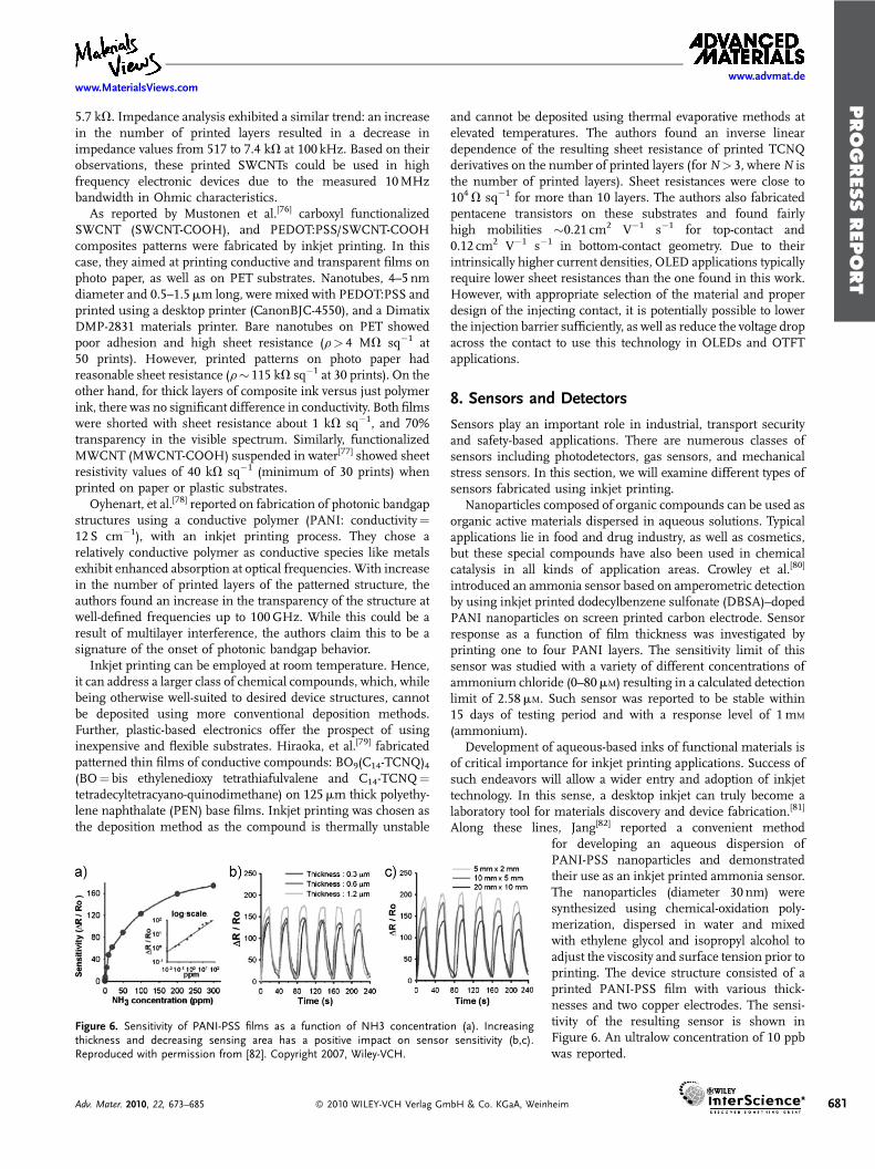
Along these lines, Jang[82] reported a convenient methodfor developing an aqueous dispersion ofPANI-PSS nanoparticles and demonstratedtheir use as an inkjet printed ammonia sensor.The nanoparticles (diameter 30 nm) weresynthesized using chemical-oxidation poly-merization, dispersed in water and mixedwith ethylene glycol and isopropyl alcohol toadjust the viscosity and surface tension prior toprinting. The device structure consisted of aprinted PANI-PSS film with various thick-nesses and two copper electrodes. The sensi-tivity of the resulting sensor is shown inFigure 6. An ultralow concentration of 10 ppbwas reported.
Figure 6. Sensitivity of PANI-PSS films as a function of NH3 concentration (a). Increasingthickness and decreasing sensing area has a positive impact on sensor sensitivity (b,c).Reproduced with permission from [82]. Copyright 2007, Wiley-VCH.
Adv. Mater. 2010, 22, 673–685 ! 2010 WILEY-VCH Verlag GmbH & Co. KGaA, Weinheim 681
PROGRESS
REPORT
www.advmat.dewww.MaterialsViews.com
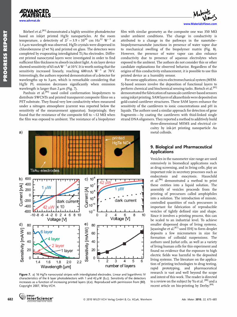
Borberl et al.[83] demonstrated a highly sensitive photodetectorbased on inkjet printed HgTe nanoparticles. At the roomtemperature, a detectivity of D*! 3.9% 1010 cm Hz12 W$1 at1.4mmwavelength was observed. HgTe crystals were dispersed inchlorobenzene (2wt %) and printed on glass. The detectors werecompleted by evaporating interdigitated Ti/Au electrodes. Differ-ent printed nanocrystal layers were investigated in order to findsufficient film thickness to absorb incident light. A six layer deviceshowed sensitivity of 65mAW$1 at 10 V. It is worth noting that thesensitivity increased linearly, reaching 600mA W$1 at 70V.Interestingly, the authors reported demonstration of a detector forwavelengths up to 3mm, which is remarkable considering thatHgTe PL emission decreases significantly when emissionwavelength is larger than 2mm (Fig. 7).
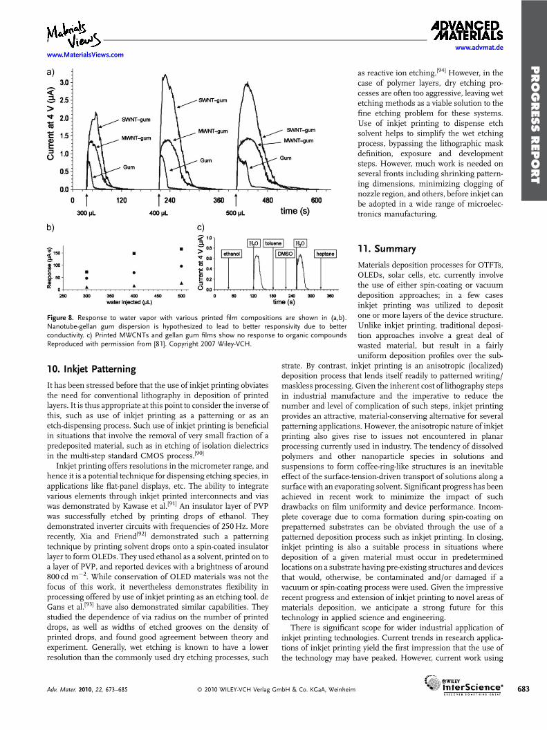
Panhuis et al.[84] used coiled conformation biopolymers todistribute SWCNTs and printed transparent composite films on aPET substrate. They found very low conductivity when measuredunder a nitrogen atmosphere (current was reported below thesensitivity of the measurement apparatus). Surprisingly, theyfound that the resistance of the composite fell to #12 MV whenthe film was exposed to ambient. The resistance of a biopolymer
film with similar geometry as the composite one was 350 MVunder ambient conditions. The change in conductivity isattributed to a change in the pathways in the nanotube–biopolymernanotube junctions in presence of water vapor dueto mechanical swelling of the biopolymer matrix (Fig. 8).However, the presence of water vapor can also enhanceconductivity due to presence of aqueous electrolytes whenexposed to the ambient. The authors do not consider this or othercandidate explanations for observed behavior. Regardless of theorigins of this conductivity enhancement, it is possible to use thisprinted device as a humidity sensor.
For some applications,micro-electromechanical system (MEM-S)-based sensors involve the deposition of functional layers toperform chemical and biochemical sensing tasks. Bietsch et al.[85]
demonstratedthefabricationofnanoscalecantilever-basedsensorsusing inkjetprinting.SAMlayersof alkanethiolsweredepositedongold-coated cantilever structures. These SAM layers enhance thesensitivity of the cantilevers to ionic concentrations and pH inliquids. The authors used a similar approach for detection of genefragments—by coating the cantilevers with thiol-linked singlestrandDNAoligomers. They reported amethod to additively build
three-dimensional MEMS and electrical cir-cuitry by ink-jet printing nanoparticle Aumetal colloids.
9. Biological and PharmaceuticalApplications
Vesicles in the nanometer size range are usedextensively in biomedical applications suchas drug screening, and in living cells, play animportant role in secretory processes such asendocytosis and exocytosis. Hauschildet al.[86] demonstrated a method to printthese entities into a liquid solution. Theassembly of vesicles proceeds from theprinting of precursors called amphiphilesinto a solution. The introduction of minute,controlled quantities of such precursors isimportant for fabrication of reproduciblevesicles of tightly defined size and shape.Since it involves a printing process, this canbe scaled to an industrial level. To achievesmaller dispensed drops of living systems,Jayasinghe et al.[87] used EHJ to form dropletdeposits a few micrometers in size forformation of colloidal suspensions. Theauthors used Jurkat cells, as well as a varietyof living human cells for this experiment andfound no evidence that the exposure to highelectric fields was harmful to the depositedliving systems. The literature on the applica-tion of printing technologies to drug testing,rapid prototyping, and pharmaceuticalresearch is vast and well beyond the scopeand intent of this work. The reader is directedto a review on the subject by Yu et al. [88] and arecent article on bio-printing by Derby.[89]
Figure 7. a) 16 HgTe nanocrystal stripes with interdigitated electrodes. Linear and logarithmic IVcharacteristics of the 6 layer photodetectors with 1 and 42mW (b,c). Sensitivity of the detectorsincreases as a function of increasing printed layers (d,e). Reproduced with permission from [80].Copyright 2007, Wiley-VCH.
682 ! 2010 WILEY-VCH Verlag GmbH & Co. KGaA, Weinheim Adv. Mater. 2010, 22, 673–685
PROGRESS
REPORT
www.MaterialsViews.comwww.advmat.de
10. Inkjet Patterning
It has been stressed before that the use of inkjet printing obviatesthe need for conventional lithography in deposition of printedlayers. It is thus appropriate at this point to consider the inverse ofthis, such as use of inkjet printing as a patterning or as anetch-dispensing process. Such use of inkjet printing is beneficialin situations that involve the removal of very small fraction of apredeposited material, such as in etching of isolation dielectricsin the multi-step standard CMOS process.[90]
Inkjet printing offers resolutions in the micrometer range, andhence it is a potential technique for dispensing etching species, inapplications like flat-panel displays, etc. The ability to integratevarious elements through inkjet printed interconnects and viaswas demonstrated by Kawase et al.[91] An insulator layer of PVPwas successfully etched by printing drops of ethanol. Theydemonstrated inverter circuits with frequencies of 250Hz. Morerecently, Xia and Friend[92] demonstrated such a patterningtechnique by printing solvent drops onto a spin-coated insulatorlayer to formOLEDs. They used ethanol as a solvent, printed on toa layer of PVP, and reported devices with a brightness of around800 cd m$2. While conservation of OLED materials was not thefocus of this work, it nevertheless demonstrates flexibility inprocessing offered by use of inkjet printing as an etching tool. deGans et al.[93] have also demonstrated similar capabilities. Theystudied the dependence of via radius on the number of printeddrops, as well as widths of etched grooves on the density ofprinted drops, and found good agreement between theory andexperiment. Generally, wet etching is known to have a lowerresolution than the commonly used dry etching processes, such
as reactive ion etching.[94] However, in thecase of polymer layers, dry etching pro-cesses are often too aggressive, leaving wetetching methods as a viable solution to thefine etching problem for these systems.Use of inkjet printing to dispense etchsolvent helps to simplify the wet etchingprocess, bypassing the lithographic maskdefinition, exposure and developmentsteps. However, much work is needed onseveral fronts including shrinking pattern-ing dimensions, minimizing clogging ofnozzle region, and others, before inkjet canbe adopted in a wide range of microelec-tronics manufacturing.
11. Summary
Materials deposition processes for OTFTs,OLEDs, solar cells, etc. currently involvethe use of either spin-coating or vacuumdeposition approaches; in a few casesinkjet printing was utilized to depositone or more layers of the device structure.Unlike inkjet printing, traditional deposi-tion approaches involve a great deal ofwasted material, but result in a fairlyuniform deposition profiles over the sub-
strate. By contrast, inkjet printing is an anisotropic (localized)deposition process that lends itself readily to patterned writing/maskless processing. Given the inherent cost of lithography stepsin industrial manufacture and the imperative to reduce thenumber and level of complication of such steps, inkjet printingprovides an attractive, material-conserving alternative for severalpatterning applications. However, the anisotropic nature of inkjetprinting also gives rise to issues not encountered in planarprocessing currently used in industry. The tendency of dissolvedpolymers and other nanoparticle species in solutions andsuspensions to form coffee-ring-like structures is an inevitableeffect of the surface-tension-driven transport of solutions along asurface with an evaporating solvent. Significant progress has beenachieved in recent work to minimize the impact of suchdrawbacks on film uniformity and device performance. Incom-plete coverage due to coma formation during spin-coating onprepatterned substrates can be obviated through the use of apatterned deposition process such as inkjet printing. In closing,inkjet printing is also a suitable process in situations wheredeposition of a given material must occur in predeterminedlocations on a substrate having pre-existing structures and devicesthat would, otherwise, be contaminated and/or damaged if avacuum or spin-coating process were used. Given the impressiverecent progress and extension of inkjet printing to novel areas ofmaterials deposition, we anticipate a strong future for thistechnology in applied science and engineering.
There is significant scope for wider industrial application ofinkjet printing technologies. Current trends in research applica-tions of inkjet printing yield the first impression that the use ofthe technology may have peaked. However, current work using
Figure 8. Response to water vapor with various printed film compositions are shown in (a,b).Nanotube-gellan gum dispersion is hypothesized to lead to better responsivity due to betterconductivity. c) Printed MWCNTs and gellan gum films show no response to organic compoundsReproduced with permission from [81]. Copyright 2007 Wiley-VCH.
Adv. Mater. 2010, 22, 673–685 ! 2010 WILEY-VCH Verlag GmbH & Co. KGaA, Weinheim 683

PROGRESS
REPORT
www.advmat.dewww.MaterialsViews.com
inkjet printing across various applications suggests that the focushas been on uniformity and two-dimensional coverage ofsubstrates. A better understanding of the flow properties ofinteracting droplets with the substrate or previously depositedlayers is likely to open up possibilities for study of bettercontrolled growth in the vertical dimension. With suitabletechnological advancements, the minimum amount of fluiddispensable can be further reduced. This reduction can be used toattempt the deposition of SAMs from very dilute solutions withlong printing times, deposition of optically active thin layers fornon-linear optics (NLO) and OLED applications, superlattices forhybrid PVs incorporating low-dimensional systems such as QDs.Use of EHJ-based techniques has recently acquired great interest,and further developments in this field are likely to address theissue of minimum resolutions achievable with printing. A greatdeal of work remains to be done in fundamental understanding ofthe fluid flow process during inkjet printing to facilitate furtheradvances in this very exciting field.
Acknowledgements
M.S. and G.E.J. would like to acknowledge funding from Nitto DenkoTechnology and Advanced Photovoltaics Center. G.E.J. would liketo thank FUJIFILM Dimatix, Inc. for theirsupport. P.D. and G.E.J.acknowledge funding from the Army Research Laboratory under theCooperative Agreement W911NG-04-2-0005. G.E.J. and H.M.H acknowl-edge the FiDiPro program and the Graduate School of Modern Optics andPhotonics, Finland.
Received: April 3, 2009Published online: August 25, 2009
[1] OE-A Roadmap for Organic and Printed Electronics, Organic Electronics
Association OE-A, Frankfurt, 2008.
[2] E. Tekin, P. J. Smith, U. S. Schubert, Soft Matter 2008, 4, 703.[3] D. Pesach, A. Marmur, Langmuir 1987, 3, 519.
[4] J. A. Lim, W. H. Lee, H. S. Lee, J. H. Lee, Y. D. Park, K. Cho, Adv. Funct.
Mater. 2008, 18, 229.
[5] J. Perelaer, P. J. Smith, E. van den Bosch, S. S. C. van Grootel,
P. H. J. M. Ketelaars, U. S. Schubert,Macromol. Chem. Phys. 2009, 210, 495.
[6] J. Perelaer, P. J. Smith, M. M. P. Wijnen, E. van den Bosch, R. Eckardt,
P. H. J. M. Ketelaars, U. S. Schubert,Macromol. Chem. Phys. 2009, 210, 387.[7] D. Bartolo, A. Boudaoud, G. Narcy, D. Bonn, Phys. Rev. Lett. 2007, 99,
174502.
[8] E. K. Hill, R. L. Watson, D. E. Dunstan, J. Fluoresc. 2005, 15, 255.
[9] H. Dong, W. W. Carr, J. F. Morris, Phys. Fluids 2006, 18, 072102.[10] J. Perelaer, P. J. Smith, C. E. Hendriks, A. M. J. van den Berg, U. S. Schubert,
Soft Matter 2008, 4, 1072.
[11] M. H. Tsai, W. S. Hwang, H. H. Chou, P. H. Hsieh, Nanotechnology 2008,
19, 335304.
[12] V. V. Khatavkar, P. D. Anderson, P. C. Duineveld, H. H. E. Meijer,Macromol.
Rapid Commun. 2005, 26, 298.
[13] A. A. Goghari, S. Chandra, Exp. Fluids 2008, 44, 105.[14] A. M. J. van den Berg, A. W. M. d. Laat, P. J. Smith, J. Perelaer,
U. S. Schubert, J. Mater. Chem. 2007, 17, 677.
[15] J.-U. Park, M. Hardy, S. J. Kang, K. Barton, K. Adair, D. K. Mukhopadhyay,
C. Y. Lee, M. S. Strano, A. G. Alleyne, J. G. Georgiadis, P. M. Ferreira,
J. A. Rogers, Nat. Mater. 2007, 6, 782.
[16] A. M. J. van den Berg, P. J. Smith, J. Perelaer, W. Schrof, S. Koltzenburg,
U. S. Schubert, Soft Matter 2007, 3, 238.
[17] A. Dodabalapur, Mater. Today 2006, 9, 24.
[18] J. Jang, Mater. Today 2006, 9, 46.[19] Y.-Y. Noh, N. Zhao, M. Caironi, H. Sirringhaus, Nat. Nanotechnol. 2007, 2,
784.
[20] H. Sirringhaus, T. Kawase, R. H. Friend, T. Shimoda, M. Inbasekaran,
W. Wu, E. P. Woo, Science 2000, 290, 2123.[21] J. Z. Wang, Z. H. Zheng, H. W. Li, W. T. S. Huck, H. Sirringhaus,Nat. Mater.
2004, 3, 171.
[22] J. Z. Wang, J. Gu, F. Zenhausern, H. Sirringhaus, Appl. Phys. Lett. 2006, 88,133502.
[23] C. W. Sele, T. Werne, R. H. Friend, H. Sirringhaus, Adv. Mater. 2005, 17,
997.
[24] S. E. Molesa, S. K. Volkman, D. R. Redinger, A. de la Fuente Vornbrock,
V. Subramanian, IEEE Int. Electron Device Meeting Tech. Digest 2004, 1072.
[25] Y. Liu, K. Varahramyan, T. Cui, Macromol. Rapid Commun. 2005, 26,
1955.
[26] A. C. Arias, S. E. Ready, R. Lujan, W. S. Wong, K. E. Paul, A. Salleo,
M. L. Chabinyc, R. Apte, A. S. Robert, Y. Wu, P. Liu, B. Ong, Appl. Phys. Lett.
2004, 85, 3304.
[27] K. E. Paul, W. S. Wong, S. E. Ready, R. A. Street, Appl. Phys. Lett. 2003, 83,2070.
[28] S. H. Ko, H. Pan, C. P. Grigoropoulos, C. K. Luscombe, J. M. J. Frechet,
D. Poulikakos, Nanotechnology 2007, 18, 345202.
[29] Y.-H. Kim, S.-M. Han, W. Lee, M.-K. Han, Y. U. Lee, J.-I. Han, Appl. Phys.
Lett. 2007, 91, 042113.
[30] V. Subramanian, P. C. Chang, J. B. Lee, S. E. Molesa, S. K. Volkman,
IEEE Trans. Components Packaging Technol. 2005, 28, 742.
[31] P. Beecher, P. Servati, A. Rozhin, A. Colli, V. Scardaci, S. Pisana, T. Hasan,
A. J. Flewitt, J. Robertson, G. W. Hsieh, F. M. Li, A. Nathan, A. C. Ferrari,
W. I. Milne, J. Appl. Phys. 2007, 102, 043710.
[32] T. Shimoda, Y. Matsuki, M. Furusawa, T. Aoki, I. Yudasaka, H. Tanaka,
H. Iwasawa, D. Wang, M. Miyasaka, Y. Takeuchi, Nature 2006, 440, 783.[33] Y.-Y. Noh, X. Cheng, H. Sirringhaus, J. I. Sohn, M. E. Welland, D. J. Kang,
Appl. Phys. Lett. 2007, 91, 043109.
[34] H. Cheong Min, S. Wagner, IEEE Electron Device Lett. 2000, 21, 384.[35] Y. Wu, Y. Li, B. S. Ong, P. Liu, S. Gardner, B. Chiang, Adv. Mater. 2005, 17,
184.
[36] S. Molesa, D. Redinger, D. Huang, V. Subramanian,Mater. Res. Soc. Symp.
Proc. (Eds: N. Fruehauf, B. R. Chalamala, B. E. Gnade, J. Jang), San
Francisco 2003, H8.3.1
[37] S. Gamerith, A. Klug, H. Scheiber, U. Schref, E. Moderegger, E. J. W. List,
Adv. Funct. Mater. 2007, 17, 3111.
[38] W. S. Wong, E. M. Chow, R. Lujan, V. Geluz-Aguilar, M. L. Chabinyc, Appl.
Phys. Lett. 2006, 89, 142118.
[39] J. Daniel, A. C. Arias, W. Wong, R. Lujan, S. Ready, B. Krusor, R. A. Street,
Jpn. J. Appl. Phys. 2007, 46, 1363.[40] M. L. Chabinyc, W. S. Wong, A. Salleo, K. E. Paul, R. A. Street, Appl. Phys.
Lett. 2002, 81, 4260.
[41] T. Sekitani, Y. Noguchi, U. Zschieschang, H. Klauk, T. Someya, Proc. Natl.
Acad. Sci. 2008, 105, 4976.[42] Y. Noguchi, T. Sekitani, T. Yokota, T. Someya, Appl. Phys. Lett. 2008, 93,
043303.
[43] Y. R. Wu, M. Singh, J. Singh, J. Appl. Phys. 2003, 94, 5826.
[44] M. Singh, Y. R. Wu, J. Singh, Solid-State Electron. 2003, 47, 2155.[45] W. J. Tseng, S. Y. Lin, S.-R. Wang, J. Electroceram. 2006, 16, 537.
[46] A. C. Arias, F. Endicott, R. A. Street, Adv. Mater. 2006, 18, 2900.
[47] T. X. Sun, G. E. Jabbour, MRS Bull. 2002, 309.[48] Y. Yoshioka, G. E. Jabbour, Adv. Mater. 2006, 18, 1307.
[49] E. Tekin, H. Wijlaars, E. Holder, D. A. M. Egbe, U. S. Schubert, J. Mater.
Chem. 2006, 16, 4294.
[50] E. Tekin, P. J. Smith, S. Hoeppener, A. M. J. van den Berg, A. S. Susha,
A. L. Rogach, J. Feldmann, U. S. Schubert, Adv. Funct. Mater. 2007, 17, 23.
[51] M. Singh, T. Kondou, H. Chae, J. D. Froehlich, S. Li, A. Mochizuki,
G. E. Jabbour, Mater. Res. Soc. Fall Meeting 2008, G13.7
684 ! 2010 WILEY-VCH Verlag GmbH & Co. KGaA, Weinheim Adv. Mater. 2010, 22, 673–685

PROGRESS
REPORT
www.MaterialsViews.comwww.advmat.de
[52] M. Singh, H. Chae, J. D. Froehlich, T. Kondou, S. Li, A. Mochizuki,
G. E. Jabbour, Soft Matter 2009 DOI: 10.1039/B903531A.
[53] H. M. Haverinen, R. A. Myllyla, G. E. Jabbour, Appl. Phys. Lett. 2009, 94,
073108.
[54] S. Shigematsu, Y. Ishida, N. Nakashima, T. Asano, Jpn. J. Appl. Phys. 2008,
47, 5109.
[55] W. R. Small, F. Masdarolomoor, G. G. Wallace, M. in het Panhuis, J. Mater.
Chem. 2007, 17, 4359.
[56] S. E. Shaheen, R. Radspinner, N. Peyghambarian, G. E. Jabbour, Appl. Phys.
Lett. 2001, 79, 2996.
[57] V. Marin, E. Holder, M. M. Wienk, E. Tekin, D. Kozodaev, U. S. Schubert,
Macromol. Rapid Commun. 2005, 26, 319.
[58] E. Holder, B. M. W. Langeveld, U. S. Schubert, Adv. Mater. 2005, 17,1109.
[59] C. N. Hoth, S. A. Choulis, P. Schilinsky, C. J. Brabec, Adv. Mater. 2007, 19,
3973.
[60] T. Aernouts, T. Aleksandrov, C. Girotto, J. Genoe, J. Poortmans, Appl. Phys.
Lett. 2008, 92, 033306.
[61] H.-W. Schock, R. Noufi, Prog. Photovoltaics: Res. Appl. 2000, 8, 151.
[62] M. A. Contreras, K. Ramanathan, J. AbuShama, F. Hasoon, D. L. Young,
B. Egaas, R. Noufi, Prog. Photovoltaics: Res. Appl. 2005, 13, 209.
[63] O. Morton, Nature 2006, 443, 19.
[64] D. Cohen, New Sci. 2007, 34.
[65] J. K. J. Van Duren, M. R. Robinson, C. Leidholm, US Patent 20070163638,
2007.
[66] V. K. Kapur, M. Fisher, R. Roe, Mater. Res. Soc. Symp. Proc. 2001,
H2.6
[67] W. Voit, W. Zapka, L. Belova, K. V. Rao, Proc. Sci. Meas. Technol. 2003, 150,252.
[68] Y. Li, C. Fu, J. Xu, Jpn. J. Appl. Phys. 2007, 46, 6807.
[69] T. H. van Osch, J. Perelaer, A. W. M. de Laat, U. S. Schubert, Adv. Mater.
2008, 20, 343.[70] H. Meier, U. Loffelmann, D. Mager, P. J. Smith, J. G. Korvink, Phys. Status
Solidi A 2009, in press.
[71] N. Zhao, M. Chiesa, H. Sirringhaus, Y. Li, Y. Wu, B. Ong, J. Appl. Phys. 2007,101, 064513.
[72] D. Huang, F. Liao, S. Molesa, D. Redinger, V. Subramanian, J. Electrochem.
Soc. 2003, 150, G412.
[73] O. Ngamna, A. Morrin, A. J. Killard, S. E. Moulton, M. R. Smyth,
G. G. Wallace, Langmuir 2007, 23, 8569.[74] J. W. Song, C. S. Han, Int. J. Precision Eng. Manuf. 2008, 9, 79.
[75] J. W. Song, J. Kim, Y. H. Yoon, B. S. Choi, J. H. Kim, C. S. Han,
Nanotechnology 2008, 19, 095702.
[76] T. Mustonen, K. Kordas, S. Saukko, G. Toth, J. S. Penttila, P. Helisto,
H. Seppa, H. Jantunen, Phys. Status Solidi B 2007, 244, 4336.
[77] K. Kordas, T. Mustonen, T. Geza, H. Jantunen, M. Lajunen, C. Soldano,
S. Talapatra, S. Kar, R. Vajtai, P. M. Ajayan, Small 2006, 2, 1021.[78] L. Oyhenart, V. V. F. Demontoux, J. P. Parneix, Microw. Opt. Technol. Lett.
2005, 44, 460.
[79] M. Hiraoka, T. Hasegawa, Y. Abe, T. Yamada, Y. Tokura, H. Yamochi,
G. Saito, T. Akutagawa, T. Nakamura, Appl. Phys. Lett. 2006, 89, 173504.[80] K. Crowley, E. O’Malley, A. Morrin, M. R. Smyth, A. J. Killard, Analyst 2008,
133, 391.
[81] Y. Yoshioka, G. E. Jabbour, Synth. Met. 2006, 156, 779.
[82] J. Jang, J. Ha, J. Cho, Adv. Mater. 2007, 19, 1772.[83] M. Borberl, M. V. Kovalenko, S. Gamerith, E. J. W. List, W. Heiss, Adv.
Mater. 2007, 19, 3574.
[84] M. in het Panhuis, A. Heurtematte, W. R. Small, V. N. Paunov, Soft Matter
2007, 3, 840.
[85] A. Bietsch, J. Zhang, M. Hegner, H. P. Lang, C. Gerber, Nanotechnology
2004, 15, 873.
[86] S. Hauschild, U. Lipprandt, A. Rumplecker, U. Borchert, A. Rank,
R. Schubert, F. Stephan, Small 2005, 1, 1177.
[87] S. N. Jayasinghe, A. N. Qureshi, P. A. M. Eagles, Small 2006, 2, 216.
[88] D. G. Yu, L.-M. Zhu, C. J. Branford-White, X. L. Yang, J. Pharm. Sci. 2008, 97,
3666.
[89] B. Derby, J. Mater. Chem. 2008, 18, 5717.
[90] R. C. Jaeger, Introduction to Microelectronic Fabrication, Vol. 5,
Addison-Wesley, Reading, MA, 1993.
[91] T. Kawase, H. Sirringhaus, R. H. Friend, T. Shimoda, Adv. Mater. 2001, 13,1601.
[92] Y. Xia, R. H. Friend, Appl. Phys. Lett. 2007, 90, 253513.
[93] B. J. de Gans, S. Hoeppener, U. S. Schubert, J. Mater. Chem. 2007, 17,3045.
[94] S. M. Sze, Semiconductor Devices: Physics and Technology, John Wiley &
Sons, New York 1985.
Adv. Mater. 2010, 22, 673–685 ! 2010 WILEY-VCH Verlag GmbH & Co. KGaA, Weinheim 685