Embed Size (px)
Citation preview
MEMBER COMPANY PROFILE
FlipChip International’s acquisition of Kulicke and Soffa’s Flip Chip Division (K&S FCD) in Phoenix, Arizona, in Feb-ruary of 2004, enabled FCI with bumping technology services that are well known in the industry. This acquisition included standard fl ip chip and UltraCSP® as bump-ing offerings and is now FCI’s Bumping Division. Since the acquisition, a special-ized polymer process named Spheron® has been commercialized and is gaining popularity as a high performance solution for high speed applications such as Radio on Chip. page 22
INDUSTRY NEWS
Kulicke & Soffa Industries has relocated its corporate headquarters. page 16
SUSS MicroTec AG has installed the latest 300 mm technology in wafer probe systems at the nanoelectronics research center IMEC in Leu-ven, Belgium. page 16
Advanced Interconnect Technologies (AIT) has announced that it is expanding its world-class assembly and test factory in Batam, Indonesia. page 16
March Plasma Systems has established direct operations in Shanghai, China, that include an Advanced Applications and Demonstration Laboratory. page 17
Pac Tech GmbH announced that Nagase and Co., a major trading company in Japan, acquired a 60% share of Pac Tech GmbH in February for an undisclosed amount. page 17
STATS ChipPAC has expanded its Quad Flat No-lead (QFN) packaging portfolio. page 18
According to fi nal results reported by Gartner, Inc., worldwide semiconductor revenue totaled $235 billion in 2005, a 5.7 percent increase from 2004. 2005 revenue surpassed the semi-conductor industry’s previous record of $223 billion set in 2000. page 19
Semiconductor equipment bookings increase 60% over April 2005 level. page 20
R ose Street Laborato-ries, the parent com-pany of FlipChip Inter-national, was founded
in 2003 with a roadmap of providing leadership in product and service support to the elec-tronics industry. RSL has been very active in the life sciences, renewable energy and homeland security markets.
Volume 10, Number 2
QUARTER TWO 2006
A Publication of The MicroElectronics Packaging & Test Engineering Council
SEMICON West returns to Moscone Center in San Francisco July 10 though 14. page 21
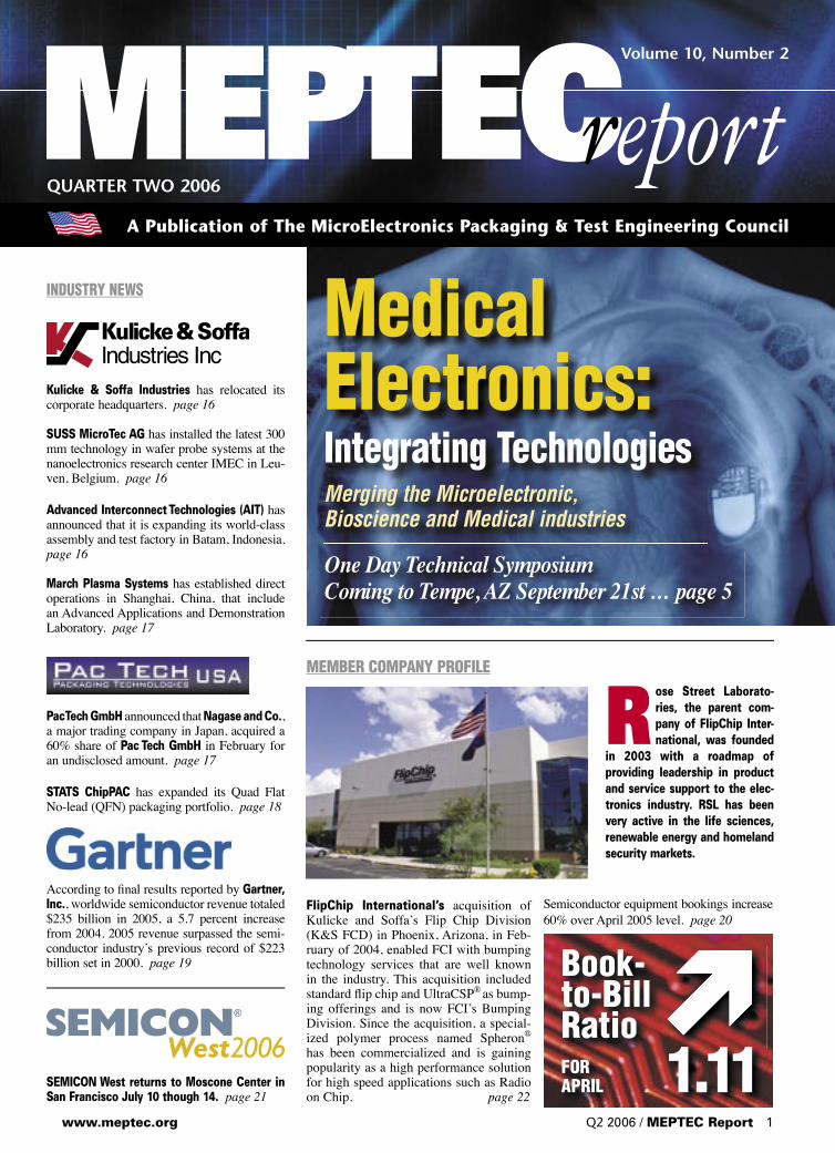
One Day Technical Symposium Coming to Tempe, AZ September 21st ... page 5
Medical Electronics: Integrating Technologies Merging the Microelectronic, Bioscience and Medical industries
Book-to-Bill RatioFORAPRIL 1.11
www.meptec.org Q2 2006 / MEPTEC Report 1
Industries Inc

unique value
Like no other—our key strengths in chemistry and metallurgy come together to solve the most complex industry challenges.With precisely the right investments in the right places at the right time,
we’re uniquely positioned to help bring your newest ideas forward.
Our ongoing research and development in chemistry, metallurgy, and
the processes that bring them together—from our 300mm facility in
Spokane, Washington, to our latest technology center in Shanghai,
China—ensure that wherever challenges arise, we’ll continue to create solutions that solve them.
And as a partner to 90% of the top semiconductor houses worldwide, our technology portfolio is
consistently at the forefront of invention, empowering the global leaders of innovation. Honeywell
Electronic Materials—delivering unmatched value today and tomorrow.
Get more information by visiting www.honeywell.com/sm/em Or call 1-408-962-2000
© 2006 Honeywell International Inc. All rights reserved.
Advanced Spin-on Materials • Electronic Chemicals • Precious Metal Thermocouples • PVD Targets & Coil Sets • Optoelectronics • Packaging
I t’s that time again...summertime, and that of course means Semicon West, when thousands in the industry con-verge on Northern California to see the latest and greatest technology in
the semiconductor industry. This year is the second since SEMI moved the entire show to San Francisco, integrating the Final Manu-facturing segment of the show into the rest of the event. We’re pleased this year to be a part of Semicon West, as a technical session contrib-utor to their TechXPOT (pronounced “Tech Spot”). According to a press release on the special sessions (see page 19), SEMI is build-ing on the “show-within-a-show” concept, and the Test, Assembly and Packaging portion will focus on innovations in test, assembly and packaging, with exhibits, displays and technical presentations. There will be two MEPTEC sessions during TechXPOT: The Packaging Roadmaps session will be held on Tuesday, July 11 from 11:00 am to 12:20 pm, and Materials for Packaging session will be held on Wednesday, July 12 from 11:00 am to 12:20 pm, and will be held in the Test, Assembly and Packaging hall, right on the show fl oor. The SEMI press release men-tioned above offers details of speakers and topics. Other organizations contributing are FSA, ITC and iNEMI. We hope you’ll stop in to see these information sessions We’re pleased to announce another new MEPTEC Advisory Board member: Bhavesh Muni of Henkel Corporation. Bhavesh is currently their Director, Global Semicon-ductor Material Business and is responsible for development and execution of global business strategy for Henkel’s semiconduc-tor packaging material business. Welcome Bhavesh! Our next event will be held on Thurs-day, September 21 and will be a divergence from our usual Bay Area venue: we’ve been invited to hold it on the Tempe campus of Arizona State University, in the beautiful Old Main building. The event, called “Medi-cal Electronics – Integrating Technologies: Merging the Microelectronic, Bioscience and Medical Industries” will be co-sponsored by ASU and the MacroTechnology Works. The symposium will be co-chaired by MEPTEC member David Ruben of Medtronics and MEPTEC Advisory Board member Nick Leonardi of CMC Interconnect Technolo-gies. See page 5 for further information.
We also offer a follow-up look on a couple of past symposiums. These follow-ups are regular features in each issue. For each event, Jody Mahaffey of JDM Resources writes a pre-symposium article wherein she previews the program, interviews participants, and sum-marizes in an article which gets distributed to the trade magazines and on-line publications. After the symposium she updates and fi nal-izes the article, and that is what you will see here. In this case the event was our special 2-day symposium on May 17-18 called “MEMS Packaging Trends: From Production to Mar-ket”. This event included a SEMI workshop on MEMS Packaging Standards, as well as an academic session where we heard about some of the leading-edge research in MEMS technology. In addition, Julia Goldstein, editor at Advanced Packaging magazine, follows up with a review of our February event on “2nd Annual The Heat is On: Ther-mal Management Solutions in Semiconductor Packaging”. See page 6 for both of these summaries. CDs of the proceedings for both of these events will soon be available on the MEPTEC website at www.meptec.org, or call Bette Cooper at the MEPTEC offi ce to order today – 650-714-1570. One of the feature articles this issue is con-
Issue HighlightsMEPTEC Events Follow-up 6
Industry Analysis 10
University News 13
Industry News 14
Member Company Profi le 22
Feature Articles
• Low Cost, High Performance 24 Silicon Packages
• Materials Declaration for 28 Everyone
• Stress Free Modeling 30
• Airfl ow Optimization for 32 Enhanced Cooling
Event Calendar 37
Editorial 38
Council UpdateVolume 10, Number 2
A Publication of The MicroElectronics Packaging
& Test Engineering Council
P. O. Box 222Medicine Park, OK 73557
Tel: (650) 714-1570 Email: [email protected]
Published ByMEPCOM
EditorBette Cooper
Design and ProductionGary Brown
Sales and MarketingKim Barber
Contributing EditorJody Mahaffey
––––––––––––––
MEPTEC Advisory Board
Seth AlaviSunSil
Jeffrey BradenBraden & Associates
Philippe BriotP. Briot & Associates
Joel CamardaSipex Corporation
Gary CatlinPlexus
Tom CliffordLockheed-Martin
Rob ColeMiTech USAJohn Crane
J. H. Crane & AssociatesJeffrey C. Demmin
TesseraBruce Euzent
Altera CorporationSkip Fehr
Julia GoldsteinAdvanced Packaging Magazine
Chip GreelyQualcomm
Anna GualtieriElle TechnologyBance Hom
Consultech International, Inc.Ron Jones
N-Able Group InternationalPat Kennedy
Gel-PakNick Leonardi
CMC Interconnect TechnologiesAbhay Maheshwari
XilinxPhil Marcoux
Corwil Technology CorporationBhavesh Muni
Henkel CorporationMary Olsson
Gartner DataquestMarc Papageorge
Semiconductor Outsourcing SolutionsJerry SecrestSecrest ResearchJim Walker
Gartner DataquestRuss Winslow
Six Sigma
––––––––––––––
MEPTEC Report Vol. 10, No. 2. Published quarterly by MEPCOM, P. O. Box 222, Medicine Park, OK 73557. Copyright 2006 by MEPTEC/MEPCOM. All rights reserved. Materials may not be reproduced in whole or in part without written permission.
MEPTEC Report is sent without charge to members of MEPTEC. For non-members, yearly subscriptions are avail-able for $75 in the United States, $80US in Canada and Mexico, and $95US elsewhere.
For advertising rates and information contact Kim Barber, Sales & Marketing at (408) 309-3900, Fax (650) 962-8684.
www.meptec.org Q2 2006 / MEPTEC Report 3
tributed by a new MEPTEC Corporate member company, Hymite. Dr. Jochen Kuhmann and Andreas Hase write about “Low Cost, High Performance Silicon Packages”. This is a very inter-esting look at how silicon as a packaging material offers exceptional thermal and electrical performance. We were pleased to have Hymite as a speaker on the same topic at our 2005 MEMS Packag-ing event; we’ll see if we can get them to come back in 2007 and give us an update. See page 24 for this informative piece. Our other feature article is an informa-tive look at “Materials Declaration for Everyone”. Dr. N. Nagaraj of Papros, Inc. offers a discussion on exchang-ing material content data in the form of Material Composition Declarations. Sometimes the practical management issues in our industry are overshadowed by the cutting-edge technology, so we’re pleased Dr. Nagaraj has taken the time to explain this important element of data management. It really is a best practice for supply chain management. Our regular Thermal Management contributor and MEPTEC Corporate member company, Advanced Thermal Solutions (ATS), writes about “Airfl ow Optimization for Enhanced Cooling”, and can be found on page 32. Norman Quesnel discusses why airfl ow char-acteristics are so important to device manufacturing. We appreciate their con-tinued contributions on this important topic. Our Editorial this issue is contrib-uted by new MEPTEC Advisory Board member, and frequent speaker at various MEPTEC symposiums, Tom Clifford of Lockheed Martin. Tom offers himself up as our “Technology Reporter”, and takes a very interesting and introspec-tive look at future technology, and what future community will be responsible for coming up with this new technology. He researched trade magazines, news-paper sources, and even high school and junior high school Science Fair pro-grams to fi nd out if our kids are focusing on more than what he calls “fashionable” technology, such as cool music gadgets, video games, etc. I think you’ll fi nd his comments and fi ndings fascinating…see page 38. If you’ve ever met Tom you’ll know that he’s a very smart, inquisitive and refl ective guy; we’ll see if we can get him to contribute more “Technology
Reporter” pieces in future issues! Our Industry Analysis coverage this issue is contributed by Bob Johnson, Klaus Rinnen, Jim Walker and Mary Olsson of Gartner Dataquest (Jim and Mary are also long-time MEPTEC Advi-sory Board members). This article takes a look at the impact on the semiconduc-tor equipment segment of the indus-try, and how historically the equipment industry responded to changing technol-ogy by succumbing to semiconductor fi nancial pressures. They are suggesting that things are changing; see page 10 for their article titled “The Evolving Changes for the Semiconductor Equip-ment Industry”. Our Member Company Profi le this issue is MEPTEC Corporate member Flip Chip International. Theirs is a really interesting success story: it tells the tale of two visionaries, Bob Forci-er, President/CEO and Dr. Joan Vrtis, CTO of Rose Street Laboratories (RSL). They wanted to provide fl ip chip and wafer level packaging services in packaging, operate globally to support worldwide marketplaces, incorporate new IP into products and services, and form a team to make this happen, and FCI was born. You’ll see that every February since 2004 FCI has hit a major milestone, and the question is asked, “Will we have to wait until next Febru-ary to hear what’s next?”. Find out by
reading their story on page 22. Our “University News” section this issue is not really about a classic aca-demic institution, but it is about a similar type of research institution that works with academia and industry alike on electronics research. This is also our fi rst coverage of an institution outside the U.S. It is IMEC, and is located in Leu-ven, Belgium. IMEC is Europe’s largest independent research center on nano-electronics and nanotechnology. They have developed a powerful network of over 500 partners including IC manu-facturers, equipment and material sup-pliers, universities, research institutes, etc. Coincidentally, we received a news release recently from SUSS MicroTec about their collaboration with IMEC by installing their latest 300mm technology in wafer probe systems at the nanoelec-tronics part of the research center. They will continue their alliance with IMEC in the following years on technology enhancements. See their story on page 13. We’d like to thank all of our con-tributors for making this a great issue. If you’re reading our publication for the fi rst time at the Semicon West show, or another of the many events where we’ll be distributing this issue, we hope you enjoy it.
Thanks for joining us! ◆
MEPTEC Welcomes NewAdvisory Board MemberBhavesh MuniDirector, Global Semiconductor Material Business Henkel Corporation
Bhavesh Muni has more than 18 years of experience in various materials for electronics assembly & semiconductor packaging. His experience ranges from hands on R&D Chemist to technical/application services and leading up to sales & marketing aspects of electronics material business. Bhavesh is cur-rently Director, Global Semiconductor Material Business at Henkel Corpora-tion, responsible for development and execution of global business strategy for Henkel’s semiconductor packaging material business. Prior to Henkel Bhavesh held positions at Thermoset, Lord Corporation; Emerson & Cuming/Ablestik; Olin Hunt Conductive Materials; and Pacifi c Polytech/Namics. Bhavesh holds an MS in Polymer Science from the University of Detroit, Detroit, MI; a BE in Chemical Engineering, REC, Srinagar, India. He has published several technical papers on Interpenetrating Polymer Networks (IPNs).◆
4 MEPTEC Report / Q2 2006 www.meptec.org
MEPTEC Council Update
R E G I S T E R O N L I N E T O D A Y A T W W W . M E P T E C . O R G
A S P E C I A L O N E - D A Y T E C H N I C A L S Y M P O S I U M
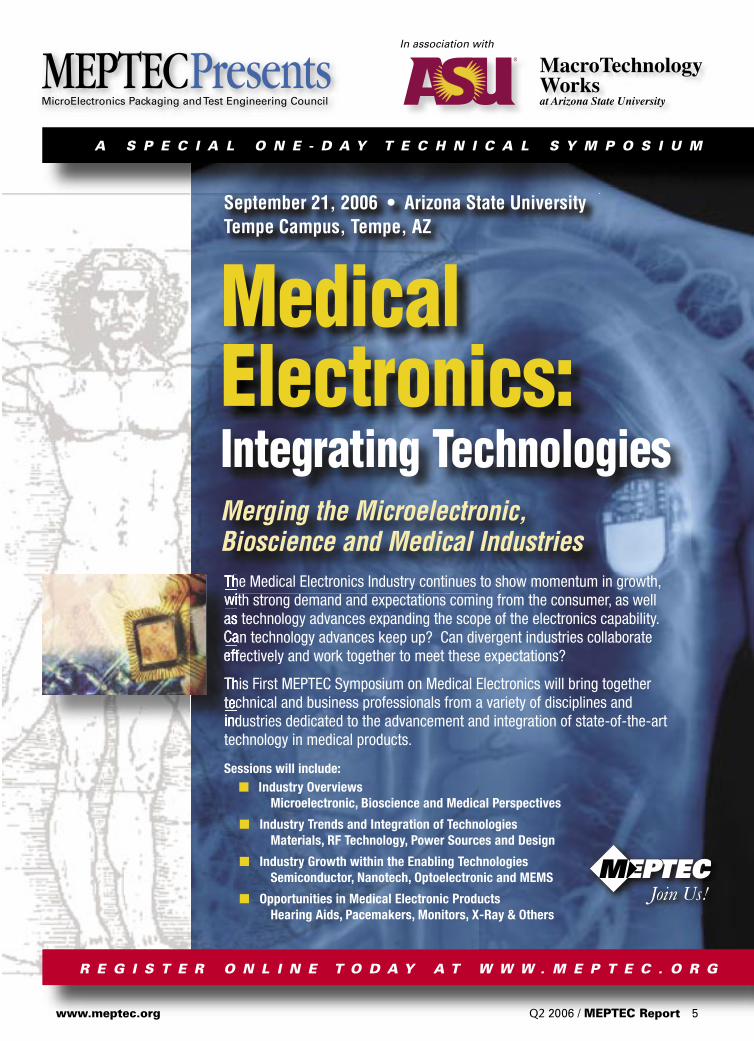
Medical Electronics: Integrating Technologies Merging the Microelectronic, Bioscience and Medical Industries
September 21, 2006 • Arizona State UniversityTempe Campus, Tempe, AZ
The Medical Electronics Industry continues to show momentum in growth, with strong demand and expectations coming from the consumer, as wellas technology advances expanding the scope of the electronics capability. Can technology advances keep up? Can divergent industries collaborate effectively and work together to meet these expectations? This First MEPTEC Symposium on Medical Electronics will bring together technical and business professionals from a variety of disciplines and industries dedicated to the advancement and integration of state-of-the-art technology in medical products.
Sessions will include: ■ Industry Overviews Microelectronic, Bioscience and Medical Perspectives
■ Industry Trends and Integration of Technologies Materials, RF Technology, Power Sources and Design
■ Industry Growth within the Enabling Technologies Semiconductor, Nanotech, Optoelectronic and MEMS
■ Opportunities in Medical Electronic Products Hearing Aids, Pacemakers, Monitors, X-Ray & Others
Join Us!
The Medical Electronics Industry continues to show momentum in growth, with strong demand and expectations coming from the consumer, as wellas technology advances expanding the scope of the electronics capability. Can technology advances keep up? Can divergent industries collaborate effectively and work together to meet these expectations?
This First MEPTEC Symposium on Medical Electronics will bring together technical and business professionals from a variety of disciplines and industries dedicated to the advancement and integration of state-of-the-art
MEPTECPresents MicroElectronics Packaging and Test Engineering Council
MacroTechnology Worksat Arizona State University
In association with
www.meptec.org Q2 2006 / MEPTEC Report 5
6 MEPTEC Report / Q2 2006 www.meptec.org
A ccording to market research com-pany YOLE Développement, the MEMS market reached $5.1 Bil-lion in 2005 and is expected to reach $9.7 Billion in 2010, rep-
resenting a compound annual growth rate of almost 15%. For the fourth year in a row, MEPTEC, the MicroElectronics Packag-ing and Test Engineering Council, brought together leading experts in the MEMS fi eld to discuss the topic as it relates to packaging in its technical symposium “MEMS Packaging Trends: From Production to Market” held on May 17 & 18th, 2006 in San Jose, CA. Some of the speakers at this conference offered insights into the changing and challenging world of MEMS. Most analysts agree that MEMS based products are forecasted to grow signifi cantly in the next ten years. We asked our experts what they thought the driving factors are for that growth. Most agree that one of the largest reasons for this growth will be new applica-tions.
Tom Clifford of Lockheed Martin Space Systems was a speaker in the End User Applications session of the symposium. He believes that, “MEMS growth depends on the product and the corresponding process. There are scores of current and potential MEMS applications of all sorts. Success depends on the profoundly new capabilities that well-designed and positioned MEMS products will provide.”
Mathieu Potin is a Market Analyst for YOLE Développement out of Lyon, France and presented in the Industry and Market Overview session of the symposium. Potin believes growth of the MEMS market goes beyond just new applications. “The develop-ment of the MEMS markets will of course be related to new applications,” explained Potin, “but the primary market growth would depend on the ability of MEMS manufacturers to supply from the component to the module.” Potin’s defi nition of a module is a MEMS product which can provide a function instead of just a sensor (component) alone. Potin believes that device manufacturers will be pushing a module offer (compared to a com-ponent offer) in order to attract added value.
Many MEMS based products such as DLP, accelerometers, pressure sensors and printers, can already be found in the general market-place. With the introduction of so many new applications we should expect to see many other products in the near future. “MEMS microphones are a major growth area for applications such as hearing aids and cell phones,” according to John Heck of Intel. “RF MEMS switches are entering the marketplace, starting in test and measurement equipment, and we may expect to see them in handheld wireless devices within the next few years. Also a wide variety of medical devices will be seen in the near future.” Heck was the Session Chair for the Enabling Technologies session.
Mark Crockett of Applied Materials said that people should expect to see MEMS sensors and actuators in more “user-centric” devices like set top boxes that sense viewer’s emotions and adapt accordingly. “We may also begin to see wearable devices to opti-mize worker productivity and effectiveness,” said Crockett, who presented in the SEMI Standards Workshop on the second day of the symposium. Potin added that, “Micro fuel cells are at a key development stage in Japan with com-panies like NEC, Fujitsu, and Toshiba, and are likely to enter the cell phone market in 2007-2008. Several service providers includ-ing NTT and KDDI have already presented mobile phone models with integrated micro fuel cells. Europe and the US are also engaged in such development through companies such as STM and Infi neon.”
Alvin Barlian, of Stanford University, believes that as the MEMS fi eld matures, more development of MEMS products will be driven by academic and industrial labs. According to Barlian, relatively newer appli-cations may include biological and chemical sensing for military and homeland security as well as transportation infrastructure systems, structural health, and environmental monitor-ing. The rebirth of aerospace and telecom-munication industries will also increase the demand for more advanced MEMS products. In addition, advances in material science play a major role in the growth of MEMS by
enabling innovative unconventional fabrica-tion processes. Barlian was a speaker in the Academic Workshop which was part of the second day of the symposium. Other than new applications, cost reduc-tion and increased reliability still remain criti-cal drivers for growth in the MEMS industry. Heck feels that signifi cant competition in the foundry business, as well as common avail-ability of MEMS-specifi c tools such as wafer bonders and deep silicon etchers are key to lowering costs. “Lower costs and improved reliability will encourage the expansion of MEMS into new markets,” added John Crane. “As improved assembly processes yield lower costs and bet-ter reliability, new markets will proliferate.” Crane represents Boschman Technology who presented in the Advanced MEMS Packaging Trends session.
Ken Yang of Honeywell believes the growth will be driven, not only by lower cost and better performance, but also by ease of manufacturing and government policy require-ments. Yang was a speaker in the Advanced MEMS Packaging Trends session. Clifford agreed that cost and reliability aren’t the only issues, saying that, “Most MEMS concepts must confront and control particulate and molecular contamination. Fur-thermore, specifi c challenges include CTE mismatch and thermal management; pass-thru of optics/gases/liquids/signals; vacuum packaging; and subtle but crucial materials compatibilities. “ For people who have been watching the MEMS market for many years, it seems that changes have come slowly. However, some signifi cant changes have occurred over the past year according to our experts. Heck explained, “MEMS foundry consolidation has started to occur, and this trend will likely continue. Also, many groups are at the cusp of commercializing in-situ, or self-packaging methods for MEMS, where the mechanical elements are self-sealed during the fabrication process. This enables the MEMS die to be treated much like a standard IC throughout the packaging process, thereby reducing packag-ing cost signifi cantly.” Clifford believes many things are chang-
MEPTEC Event Follow-up
MEMS Packaging – The Saga ContinuesJody Mahaffey JDM Resources
Presented by 5.17.065.17.06S A N J O S E • C A L I F O R N I A
A M E P T E C T W O - D A Y T E C H N I C A L S E S S I O N
S A N J O S E C A L I F O R N I A
MEMSPackaging Trends: From Production to MarketLarge Volume Drivers for MEMS Technologies
www.meptec.org Q2 2006 / MEPTEC Report 7
ing for MEMS. “Certainly one enabler is maturing design software keyed to multi-physics solutions and to the particular fab pro-cess,” explained Clifford. “Another is growing materials expertise, riding on nano-lab devel-opments. Another enabler might be turn-key development services structured to ease and accelerate the painful transition from concept to manufacturable prototype. Another bright light is the emergence of ‘packaging’ in aca-demia, as a respected and pivotal skill-set.” As new MEMS devices are developed, the packaging industry will continue to struggle with the question of whether to use exist-ing technology or develop new technology. This question becomes even more important when getting MEMS products into high vol-ume. Many people are divided on this. Heck believes that current packaging solutions will continue to evolve and drive down cost, but also new packaging methods will begin to arrive in commercially-available products in the near future. “In order to get to high volume production,” explained Heck, “ultra-low cost packaging methods are needed, both in the form of cost reduction on existing methods (such as glass frit wafer bonding), and the advent of new self-sealed MEMS devices, which will enable signifi cant cost reduction.” Clifford agreed that both existing and new technology will be needed depending on the product. “Some, including hermitic fl uidics, optics, integrated sensors, etc. might currently be package-limited. Others might work fi ne in tailored conventional or vacuum-fi nessed packages. In every case, the package is a major challenge.” But many people, like Chris Lee of Quantum Leap Packaging, feel that exist-ing packaging must be made to work in order to keep costs low. To this end, according to Lee, companies like Quantum Leap are com-bining existing packaging technology with new material sets such as QLP’s Quantech™ high performance polymer material to meet the changing demands. “As MEMS devic-es become more complex,” explained Lee, “devices are much more stress sensitive and prone to lower performance yields. Managing the device stress is a key in packaging in high volume.” Quantum Leap Packaging presented in the Enabling Technologies session. Crane added, “As MEMS products have migrated from ceramic packages to BGA and/ or QFN package types, the ability to move to high volume production has become easier and easier.” One of the biggest questions for packaging MEMS has always been and continues to be, where is the packaging done, in the front-end or the back-end? Both sectors are working on new packaging technology which will enable the proliferation of MEMS. “In-situ packaging is beginning to pay off,” according to Heck. “This technology comes directly from the front-end fabrication side.”
Yang agreed that wafer level packaging and wafer level vacuum packaging done at the front-end are critical to move MEMS for-ward. Crane believes that the ability to success-fully mold exposed die MEMS, such as fi nger print sensors or optical sensors, using trans-fer molding and fi lm assisted molding, has allowed for signifi cant assembly cost savings and improved capability. Film assisted molded products are free of mold compound fl ash and bleed. Lower cost and a reliable process at the back-end have enabled such MEMS devices to proliferate. There are other areas of concern for MEMS beyond packaging. One of these is Intellectual Property. With the increasing trend toward overseas manufacturing in the past few years, IP has become a critical issue in all semiconductor areas and perhaps more so for MEMS products. Clifford believes IP is a bigger problem for MEMS. He explained, “IP resides in and must accommodate the one fact that characterizes all MEMS products: the inseparable linkage of design / process / material / fab tooling / test methodologies / process techniques / etc. Any IP and business arrangement (licensing, scale-up, product pro-liferation, supply-chain expansion, etc.) must deal with that.” Heck agreed saying, “MEMS devices are so much more process-dependent than IC’s – you can easily port a new CMOS design from one foundry to another. But the IP inher-ent in a MEMS device is in both the design AND the process. Therefore foundries and companies may possess key differentiators based on processes they develop.” Another area of concern for MEMS is standardization. This year’s MEPTEC con-ference was extended to two days to include a half-day workshop, in conjunction with SEMI, to discuss standardization for MEMS. MEMS offers a unique challenge when it comes to standardization because so many of the devices are applications specifi c. “Appli-cations that are customized, generally require greater up front cost to achieve economies of scale,” explained Crockett. “Standardization and level of diffi culty will be driven by a variety of market forces. Unique applications will only leverage standardized solutions if the standards exist. Today, such standards for MEMS are not an option. As individual solu-tions proliferate, advantages in standardized solutions grow. For example, if fi ve products perform the same function to a customer and only one of those products offers features in compatibility and lower cost of ownership through standardization, then the decision of which product to buy is simple. Establishing this differentiation is critical in newly shaped markets.” Heck believes that because MEMS devic-es are all made for different purposes and in different markets, standardization will only
work at a very basic level. “We already have several relatively standard process modules for MEMS. For example, glass frit wafer bonding is so common these days that it may be considered a standard; this is in part due to the availability of wafer bonding and screen printing tools. I don’t think we will ever see full processes that are standard in the sense that many devices with different functions can be made with a single MEMS process.” Though it may be diffi cult, standardization is still important, even with application spe-cifi c MEMS products, according to Yang. “At least individual processes should be standard-ized so that you can use any subset of them to apply to your specifi c process set. It can then enable the foundry to group similar processes together to make a volume production from various products.” With or without standardization, the MEMS market continues to grow. According to Marlene Bourne of Bourne Research, funding of MEMS start-ups exceeded $500 million in 2005, with the average funding received per round at approximately $13 mil-lion. Bance Hom of Consultech Internation-al and Symposium Co-Chair said, “MEMS start-ups today are more market driven rather than technology driven…more direct applica-tion now, rather than pie in the sky fantasy we may have seen in the past.” One thing is for certain, even with all the issues and challenges facing MEMS, the technology is here to stay and getting stronger every day. ◆
Julia Goldstein Advanced Packaging Magazine
T hermal management continues to be a “hot” area, and MEPTEC’s second annual “The Heat is On” sympo-sium on February 16 packed the hall despite the plethora of events
covering the topic. Keynote speaker Herman Chu of Cisco divided cooling into two cat-egories – heat transport and heat transfer – and explained that effi cient heat transfer is critical
MEPTEC Event Follow-up
2nd Annual
The Heat Is On: Thermal Management Solutions in Semiconductor Packaging
2.16.06
A M E P T E C O N E - D A Y T E C H N I C A L S E S S I O N
2.16.06S A N J O S E • C A L I F O R N I A
Presented by 5.17.06S A N J O S E • C A L I F O R N I A
A M E P T E C T W O - D A Y T E C H N I C A L S E S S I O N
MEMSPackaging Trends: From Production to MarketLarge Volume Drivers for MEMS Technologies
for data centers. Customers aim to achieve suf-fi cient cooling using traditional technologies, preferring to avoid liquid cooling and other technologies that require infrastructure change. Reliability, availability and serviceability, as well as cost, are all hurdles for new technol-ogy. Chu suggested that the push to minimize energy usage could drive future data centers to be rated on effi ciency, similar to the “Energy Star” ratings on home appliances.
Professor Van Carey from UC Berkeley discussed the relationship between the theo-retical maximum heat fl ux removal rate for a vaporization process and heat fl ux achieved in mini and micro heat pumps. The ratio between the actual and maximum heat fl ux is one mea-sure of the effi ciency, which can be increased by optimizing the coolant pressure and select-ing a mixture of coolants, for example water and alcohol.
Debendra Malik of Intel discussed the 2005 International Technology Roadmap for Semiconductors (ITRS) and stated that the ITRS recognizes that packaging is a limiting factor toward improving cost and performance, and that thermal management is given signifi -cant attention in the Assembly and Packaging chapter. The focus is hot spot mitigation using heat spreaders or thermo-electric cooling. Thermal interface materials (TIMs), spreader design and cooling technology are listed as areas for improvement.
While ITRS is just now recognizing the need to focus on thermal management, heat dissipation has been addressed for decades. Sandra Winkler of Electronic Trend Pub-lications described solutions from the 1950s that used metal screws and thermal grease to conduct heat away from power transistors. Winkler gave an overview of current ther-mal management materials as well, including TIMs, fans, heat pipes, and cold plates. She described substrates containing metal layers specifi cally designed to act as heat spreaders.
Devesh Mathur of Honeywell discussed the connection between the surface condi-tion of heat spreaders (fl atness, roughness, plating) and TIM performance by showing thermal resistance tests of TIMs using various test blocks. Mathur also described new TIMs, including polymer solder hybrids fi lled with a high conductivity fi ller and low melting solder. During processing, the solder melts and sur-rounds the fi ller, providing a direct thermal path through the thickness of the TIM. Scott Allen of Henkel described a two-part adhesive TIM applied in separate beads, which then mix when the components (a package and a heat sink, for example) are assembled. Since these TIMs are solid materials they tend to perform better than chemically activated TIMs on ceramic packages, presumably since the solvent in activated materials can absorb into the ceramic, reducing TIM effectiveness. Heat-
cured TIMs are another solution for ceramic packages. The thermal performance of heat sink base plates can be improved by using a vapor cham-ber instead of solid copper or by increasing the thickness of the base plate, as Kaveh Azar of Advanced Thermal Solutions explained. He discussed the diffi culty in achieving suffi cient fl ow rate in micro-pumps and proposed an alternative solution, a BGA with a built-in, water-cooled heat spreader. Hot spot mitigation was a recurring theme, and Nanda Gopal of Gradient Design Auto-mation warned package designers to consider the chip as a dynamic device with variable temperature distribution rather than a simple heat source in their models. Gopal described the benefi ts of 3D thermal design incorporating input from both chip and package designers.
James Forster of Wells-CTI described a solution that actively controls the temperature and voltage applied to individual socketed packages during burn-in, holding them at the desired burn-in temperature and turning them off individually if they fail, while maintaining the burn-in oven at a lower temperature. This technology works for low power devices, but higher power devices can require passive or active cooling during test. Jerry Tustaniwskyj of Unisys discussed incorporating both heating and cooling capability into test sockets. ◆
MEPTEC Event Follow-up
The Evolving Changes for the Semiconductor Equipment Industry Bob Johnson, Klaus Rinnen, Jim Walker and Mary OlssonGartner Dataquest
MEPTEC Industry Analysis
T he steady and relentless advance-ment of semiconductor manu-facturing technology provides the foundation for the long-term growth of the industry. As sum-
marized by Moore’s Law in its various forms, the cost to produce a single func-tion, whether it be a bit of memory or a single gate on a logic chip, has decreased by about 50 percent every two years since the dawn of the integrated circuit age in the 1960s, and there is every expectation that this will continue. This progress in design and manufac-turing technology was neither easy nor inexpensive. Over the years, the industry created a methodical approach to new technology development that has served it well. Basic research in advanced semicon-ductor manufacturing technology is car-ried out by the leading integrated device manufacturers (IDMs) (Intel, Samsung, TI, Infineon Technologies, Renesas Tech-nology, Toshiba and others) or through industry technology development alliances (for example, the IBM alliance with AMD, Chartered Semiconductor Manufactur-ing, Samsung, Sony and Infineon). This research is turned into plans for future technology development at the detailed process level. In a parallel effort, the major semiconductor manufacturers from around the world, working through Inter-national Sematech, develop and publish the International Technology Roadmap for Semiconductors, which delineates indus-try consensus regarding the directions and new processes needed for future semicon-ductor production. Although the semiconductor manufac-turers develop the overall process flows at the fab level – and may even develop specific processes in their labs – it is gen-erally the equipment companies that turn these recommendations into production-worthy equipment when it is needed. This model worked reasonably well as long as the majority of the advances needed for the next technology node required scaling existing technology. In most cases, the technology risks were few, and equipment manufacturers could meet most of the
demands of the next process generation with upgrades to existing products. This model frequently broke down if new technologies or major changes in materials were needed. In such cases, equipment R&D efforts must begin years before production process development at the semiconductor manufacturers. Initial schedules are developed with milestones for evaluation tools but with no guarantee of market adoption. The introduction of new technologies was often delayed for years beyond initial expectations because new life was found for existing methods. Some prime examples of this were in the lithography field. For example, 248-nano-meter (nm) deep ultraviolet lithography was initially developed for implementa-tion in the late 1980s, but it didn’t make the mainstream until almost 10 years later. X-ray lithography was once touted to be the next technology after 248 nm, but that never happened. Originally, 193-nm lithography was considered a requirement for 0.18-micron production, but the indus-try waited four more years until 90 nm started production. Once viewed as essen-tial for 65-nm production, 157-nm lithog-raphy dropped off the road map entirely. On the materials side, low-k dielectrics, tungsten, high-k gate materials and others have all seen their deployment slip from initial projections by years. Although each of these developments involved a limited portion of the industry, the move to 300-millimeter (mm) wafers strained the resources of the entire equip-ment industry. Originally scheduled for initial widespread use in 1997 or 1998, it wasn’t until 2003 and 2004 that the first large 300-mm fabs ramped up fully. As a result of this slip and the continued large R&D investment required – with no returns for an extended period – the return on investment (ROI) in 300-mm technolo-gy development for equipment companies plummeted. Looking forward, the need for the development of new processes and new materials increases with each new technol-ogy node. Although lithography appears to have settled at the 193-nm technology
node for another couple of generations, new materials will be needed for each node as the industry progresses. But there is no definitive list of necessary new pro-cesses. Each new development undertaken by the equipment companies faces the risk that its ultimate acceptance by the industry will be either delayed or indefinitely post-poned. These financial risks are becoming sig-nificant and are increasing at a time when the industry is facing lower growth rates and tighter margins. Lower profitability breeds risk aversion and creates an envi-ronment in which equipment companies will be hesitant to make the necessary investments in process R&D without some reasonable guarantee of a decent ROI on the project. Thus, the question of whether the industry can keep on the path dictated by Moore’s Law for the next decade or so depends not as much on whether we can develop the necessary technology, but on whether it can be done profitably with rea-sonable and manageable financial risks.
Gartner Dataquest Perspective A number of significant market and structural trends facing the industry will lead to a rethinking of traditional business models for developing new technology. Each of these trends leads to a market demonstrating many of the characteris-tics of a mature industry: slower growth, tighter margins and fewer players. Gartner Dataquest has developed a series of Strate-gic Planning Assumptions as listed below that can help guide long-range planning efforts of industry participants. 1. The growth rate for the wafer fab equipment (WFE) market will paral-lel that of the semiconductor market through 2014. During the past few years, the over-all growth of the semiconductor market has slowed as it moved from a high-growth emerging market segment to a more mature, but still dynamic, industry. Present forecasts show that the long-term growth of the semiconductor industry has
10 MEPTEC Report / Q2 2006 www.meptec.org
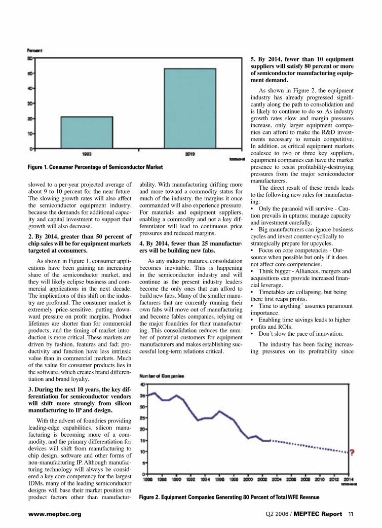
slowed to a per-year projected average of about 9 to 10 percent for the near future. The slowing growth rates will also affect the semiconductor equipment industry, because the demands for additional capac-ity and capital investment to support that growth will also decrease. 2. By 2014, greater than 50 percent of chip sales will be for equipment markets targeted at consumers. As shown in Figure 1, consumer appli-cations have been gaining an increasing share of the semiconductor market, and they will likely eclipse business and com-mercial applications in the next decade. The implications of this shift on the indus-try are profound. The consumer market is extremely price-sensitive, putting down-ward pressure on profit margins. Product lifetimes are shorter than for commercial products, and the timing of market intro-duction is more critical. These markets are driven by fashion, features and fad; pro-ductivity and function have less intrinsic value than in commercial markets. Much of the value for consumer products lies in the software, which creates brand differen-tiation and brand loyalty.
3. During the next 10 years, the key dif-ferentiation for semiconductor vendors will shift more strongly from silicon manufacturing to IP and design. With the advent of foundries providing leading-edge capabilities, silicon manu-facturing is becoming more of a com-modity, and the primary differentiation for devices will shift from manufacturing to chip design, software and other forms of non-manufacturing IP. Although manufac-turing technology will always be consid-ered a key core competency for the largest IDMs, many of the leading semiconductor designs will base their market position on product factors other than manufactur-
ability. With manufacturing drifting more and more toward a commodity status for much of the industry, the margins it once commanded will also experience pressure. For materials and equipment suppliers, enabling a commodity and not a key dif-ferentiator will lead to continuous price pressures and reduced margins. 4. By 2014, fewer than 25 manufactur-ers will be building new fabs. As any industry matures, consolidation becomes inevitable. This is happening in the semiconductor industry and will continue as the present industry leaders become the only ones that can afford to build new fabs. Many of the smaller manu-facturers that are currently running their own fabs will move out of manufacturing and become fables companies, relying on the major foundries for their manufactur-ing. This consolidation reduces the num-ber of potential customers for equipment manufacturers and makes establishing suc-cessful long-term relations critical.
5. By 2014, fewer than 10 equipment suppliers will satisfy 80 percent or more of semiconductor manufacturing equip-ment demand. As shown in Figure 2, the equipment industry has already progressed signifi-cantly along the path to consolidation and is likely to continue to do so. As industry growth rates slow and margin pressures increase, only larger equipment compa-nies can afford to make the R&D invest-ments necessary to remain competitive. In addition, as critical equipment markets coalesce to two or three key suppliers, equipment companies can have the market presence to resist profitability-destroying pressures from the major semiconductor manufacturers. The direct result of these trends leads to the following new rules for manufactur-ing:• Only the paranoid will survive - Cau-tion prevails in upturns; manage capacity and investment carefully. • Big manufacturers can ignore business cycles and invest counter-cyclically to strategically prepare for upcycles. • Focus on core competencies - Out-source when possible but only if it does not affect core competencies. • Think bigger - Alliances, mergers and acquisitions can provide increased finan-cial leverage. • Timetables are collapsing, but being there first reaps profits. • Time to anything” assumes paramount importance. • Enabling time savings leads to higher profits and ROIs. • Don’t slow the pace of innovation. The industry has been facing increas-ing pressures on its profitability since
Figure 1. Consumer Percentage of Semiconductor Market
Figure 2. Equipment Companies Generating 80 Percent of Total WFE Revenue
www.meptec.org Q2 2006 / MEPTEC Report 11
MEPTEC Industry Analysis
the mid-1990s, when the long-term rev-enue trend turned downward. Although the initial impact of this was obscured by the wild gyrations of the dot-com boom-and-bust cycle, the results have been the same: increased efforts to be more cost-efficient across the board. This approach is evidenced by the increasing importance of cost of ownership on equipment suppli-ers in the late 1990s and by the industry dictating increased capital and materials efficiency for 300-mm equipment. Many of the major semiconductor manufacturers have formed technology alliances to allevi-ate the costs of leading-edge research. The pressure to develop new process and new equipment is still directly on the equip-ment manufacturers, which are expected to develop new processes on demand, with little or no guarantee of an accept-able return on their R&D investment or even assurances that the newly developed technology will be selected for production. The current practice is to encourage multi-ple equipment suppliers to solicit competi-tive parallel developments and then stage a winner-take-all, best-of-breed competition for the production business. Although this approach may lead to slightly superior processes in the short run, the long-term effect is an inefficient use of scarce R&D
resources on an industry-wide level. As the relentless march of new technol-ogy continues, these financial pressures will continue to weigh on even the largest equipment companies. This factor leads to the final Strategic Planning Assump-tion……. 6. By 2014, the existing R&D model will have to change drastically; equipment companies will not be able to afford product development with no guaran-teed ROI. A number of possibilities will provide acceptable ROIs for equipment company R&D in the near term:• Consider equipment company process development alliances and mergers similar to the technology development alliances in the semiconductor arena. • Demand a firm purchase commitment before agreeing to develop specialized processes. Don’t agree to an open-ended development project that has no guar-antee of an acceptable ROI. Consider a nonrecurring engineering model to fund development of unique processes. Make the semiconductor manufacturers share the financial risk. • Create joint technology development consortia between semiconductor manu-
facturers and semiconductor equipment manufacturers. Shift the focus from com-petitive best-of-breed tool evaluation to competitive equipment supplier evaluation so that participation in joint development efforts guarantees equipment purchases. Some consortia, such as IMEC in Europe and Albany Nanotech, are already involv-ing major equipment companies.
Summary Historically, the industry has relied on the big semiconductor manufacturers putting pressure on the smaller equipment suppliers to meet their technology and cost objectives, with little or no consid-eration of the consequences. The equip-ment industry responded by succumb-ing to semiconductor financial pressures. The stakes for the entire industry are too great for this modus operandi to continue. More than ever, future industry growth depends on achieving the cost and per-formance goals of Moore’s Law, but it is getting increasingly difficult to do so. The industry’s lifeblood is its manufacturing technology, and it must develop new and more-effective ways to maximize returns from an increasingly scarce R&D dollar. ◆
the new world ofadvanced packaging
member of Besi group
Fico is founded in 1956 and since 1995 part of the Besi group (BE Semiconductor Industries N.V.)Fico BV, Ratio 6, 6921 RW Duiven, The Netherlands, Tel.: +31 263196100, Fax: +31 263196200, [email protected], www.besi.com
Fico Singulation MISS II+Interposer singulation system for BGA,CSP and QFNExciting new features to be introduced this year:• Sorter head now allows sorter UPH of more than 18k• User interface with new functionality for easy product set up • Auto Saw Diameter correction that requires zero cycle time
and measures the blade diameter every single product strip• More features to be announced later this year
Fico AMS-WRevolutionary MAP molding system• Double output: minimum cycle time and
optimized design • Low investment costs • Up to 40% reduction in cost of ownership • Up to 25% compound reduction • Mold open time only 12 sec.• Dynamic temperature control • Top edge gating (no gold layer required!) • 50% floor space reduction
Celebrating 50 years of Innovation
Fico BrightLineTM
With automatic tray handlerYour ultimate flexible high speed Memory Cardsingulation solution:• Modular machine concept• Free programmable curve linear cutting• No consumable usage• Integrated ultra sonic product cleaning• High UPH (up to 2200 for micro SD)• Inspection & Sort functionality• Low noise level (<75 dB)• High Flexibility: 1 system for all card types Fico also offers a full range of modules and toolsfor a big variety of IC's to cover most processes such asLaser Marking, Singulation, Inspection, Off-loadingand Sorting into Tube, Tray or Bulk.
MEPTEC
IMEC – Research Center on Nanoelectronics and Nanotechnology Three to ten years ahead of industrial needs
www.meptec.org Q2 2006 / MEPTEC Report 13
A s Europe’s largest independent research center on nanoelec-tronics and nanotechnology, IMEC has over 1,450 peo-ple from all over the world
working together in this institute with headquarters in Leuven, Belgium. They develop design methodologies, IC process and packaging technologies and enabling technologies for the electronic systems of the future. IMEC’s research bridges the gap between fundamental research at uni-versities and technology development in industry. Its unique balance of processing and system know-how, intellectual proper-ty portfolio, state-of-the-art infrastructure and its strong network of companies, uni-versities and research institutes worldwide position IMEC as a key partner for shap-ing technologies for future systems.
A Broad Range of Research Activities: IMEC’s Strategic Research Programs IMEC’s know-how on this broad range of research topics is gathered in sev-eral strategic research programs. First, to cope with the ever continuing scaling of transistor dimensions, IMEC has set up a centralized research platform. Here, leading IC-manufacturers, together with renowned equipment and material suppli-ers collaborate to fi nd innovating solutions for the sub-45nm technology nodes. The platform includes technology programs on lithography, substrate modules, gate stack, interconnects, ultra-clean process-ing, emerging devices, germanium devices
and others. Next to these ‘core’ programs, technologies to add extra functionalities to the chip are being developed. Meanwhile, IMEC looks further into the future. New technologies like carbon nanotubes, semi-conducting wires and spintronics shall be needed within ten to fi fteen years to explore the possibilities of semiconductor applications. The fundamental knowledge for these innovations is already studied at IMEC. IMEC’s portfolio also contains poly-mer-based electronics, a promising tech-nology for fl exible, light and cheap micro-electronic systems. While fi rst applications already hit the market – displays based on organic light-emitting diodes (OLED) – future applications include advanced
memories, smart clothing, radio-frequency identifi cation (RFID) tags, chemical sen-sors, solar cells and biosensors. IMEC studies different applications of organic electronics, including transistors, diodes, memories, solar cells and biosensors. In the fi eld of renewable energy sources, IMEC improves the technology for solar cells based on crystalline silicon and organic materials and also high-effi ciency photovoltaic stacks for space applications. Moreover, adaptation of the electricity grid architecture and the implementation of energy storage devices are examined. IMEC has also set up a strategic research program ‘effi cient power’ that focuses on developing high-effi ciency/high-power systems, beyond the sili-con limits, enabled by GaN technology. The program addresses three application domains: RF power amplifi cation, switch-ing devices for power conversion and, to a lower extent, optoelectronics. In the coming years, microsystems will have an increasing impact on our daily lives and wellbeing. Microsystems inte-grate multiple technology domains into small autonomous sensors with a variety of functions like detection, data process-ing and wireless communication. These miniaturized systems can create a network that communicates with the environment. Application domains include healthcare, industrial processing, food-quality control and the manufacturing of intelligent cloth-ing. IMEC develops basic technologies for these autonomous sensor networksand therefore bundles its expertise in low-
Katrien MarentCorporate Communication ManagerIMEC
IMEC’s ultra modern research facility is continuously expanding.
In IMEC’s 300mm cleanroom, solutions for the sub-45nm technology nodes are being investi-gated.
University News

power data processing, wireless commu-nication, interconnection and packaging, alternative energy sources and sensors. This research is conducted in the Holst Centre in Eindhoven, The Netherlands, established in 2005 as an initiative of IMEC and the Dutch research institute TNO. The Holst Centre has to develop into an internationally recognized research institute for the future generation of wire-less autonomous transducer solutions and systems-on-foil. In its M4 program, IMEC develops the necessary building blocks to create the future multi-mode multimedia ter-minal. This terminal will offer ubiqui-tous broadband multimedia access, served through broadband wireless communica-tion. To realize this, several technological roadblocks have to be overcome, such as increased multimedia encoder/decoder complexity, seamless switching mode across different communication standards, increasing device cost and power con-sumption due to increased functionality and fast time-to-market.
IMEC’s Advanced Packaging and Interconnect Center (APIC) IMEC’s strategic program on advanced packaging and interconnection technolo-gies focuses on bridging the so-called ‘interconnect gap’ between circuit and system, heterogeneous integration of RF components and thermal management in high-density devices. The extreme minia-turization of transistors has a large impact on packaging and interconnection tech-nologies. While the size of the chip is being reduced, the amount of input-output control pads does exactly the opposite. Assembly on for example printed circuit boards therefore becomes increasingly difficult. To solve this problem, IMEC develops a multilayer thin-film technol-ogy, which consists of multiple thin lay-ers of metal and dielectric materials. The same technology can be used to protect vulnerable structures like MEMS in the early stages of packaging. When applied on active wafers, the technology is con-sidered a wafer-level packaging (WLP) technology. Thin-film WLP technology can be used to realize on-chip flip-chip redistribution layers, for on-chip digital transmission lines, and for integration of high-quality RF passives. When thin-film technology is applied on an intermediate glass or high-resistivity Si substrate, it is considered a thin-film system-in-a-pack-age (SiP) technology or MCM-D. To make even smaller systems with increased functionality, IMEC has several activities on 3D-integration and (ultra-thin) chip stacking. First of all, 3D-SiPs are developed which are complete sys-
tems-in-a-package stacked on top of each other. This approach ensures a high yield since each sub-SiP can be tested individually ensuring that only ‘good’ SiPs are used in the 3D stack. A second approach makes use of WLP techniques where 3D interconnects are created in a post-IC passivation process. A variant of this approach, called ultra-thin chip stack-ing (UTCS), uses thinned chips, which are embedded in thin-film interconnect layers. A third approach, called 3D-stacked IC (SIC), makes the connections between the different chips during IC processing. Within its strategic program, IMEC addi-tionally focuses on the thermal character-ization of packages and the development of advanced cooling systems.
Collaboration and Training Opportunities Collaboration in Flanders, Europe and the rest of the world is of the uppermost importance for the success of the IC industry and the growth of the knowl-edge economy. This is why IMEC has set up a large network of partners (over
500), including IC manufacturers, equip-ment and material suppliers, universities, research institutes, etc. Through a unique collaboration model, based upon sharing of knowledge, talent, costs, risk and intel-lectual property, industrial researchers are integrated in IMEC’s research teams. As a result, they gather their forces to tackle technological challenges the IC industry is facing. This strategy has become the only right one to survive in a world of technological challenges, million-dollar investments and fierce competition. In the field of nano-electronics, manag-ers, engineers and researchers must also be kept abreast of the latest technological developments. IMEC’s microelectronics training center (MTC) therefore organizes courses and workshops for a variety of target groups. A broad scope of issues is addressed, ranging from IC process tech-nology, chip- and system design to basic knowledge on IC technology, biology and multimedia. IMEC also supports teachers of Flemish schools and universities. More-over, IMEC offers an international plat-form called ‘Center for Advanced Learn-ing in Information Technologies (CALIT)’ where CEOs, policy makers and scientists can meet and exchange ideas. ◆
IMEC is headquartered in Leuven, Belgium, and has representatives in the US, China and Japan. Its staff of more than 1450 people includes more than 500 industrial residents and guest research-ers. In 2005, its revenue was EUR 197 million. For further information on IMEC visit www.imec.be or contact [email protected].
MEPTEC University News
14 MEPTEC Report / Q2 2006 www.meptec.org
3D-stacked chips assembled on a printed circuit test board using leadfree solder joints.
Wafer-to-wafer bonding tool.
Please join us at the industry’s best technicalconference on electronic assembly and advanced packaging.
Common Ground. Common Goals. Uncommon Potential.
For information, call 952-920-7682 or visit www.smta.org
September 24 - 28, 2006In conjuction with Assembly Technology Expo
Donald Stephens Convention CenterRosemont, Illinois
7.875X10.875 5/31/06 9:06 AM Page 1
K&S Relocates Corporate HeadquartersFORT WASHINGTON, PA – Kulicke & Soffa Industries has relocated its corporate head-quarters to a new building in Fort Washington, Pennsylvania. The company will maintain its current telephone numbers and email addresses. Please ensure that all of your business correspondence is directed to their new cor-porate address at Kulicke and Soffa Industries, Inc., 1005 Vir-ginia Drive, Fort Washington, PA 19034
SUSS and IMEC to Develop Measurement Tools for Latest TechnologiesMUNICH, GERMANY – SUSS MicroTec AG has installed the latest 300 mm technology in wafer probe systems at the nanoelectronics research cen-ter IMEC in Leuven, Belgium. Both PA300PS ProbeShield® semiautomatic probe systems with ReAlign™ and Contact-View™ technology and PA300 probe systems for RF-noise and S-parameter measurements have been installed. An agree-ment has been made for further collaboration on enhancing 300 mm probe systems in the fol-lowing years. “We are very pleased to sign this agreement with IMEC, Europe’s leading independent nanoelectronics research cen-ter,” said Dr. Claus Dietrich, Managing Director of the Test Systems division at SUSS MicroTec. “This collaboration proves SUSS MicroTec is offer-ing the latest technology for advanced wafer probing, like the unique ReAlign and Con-tactView solutions. Further-more, it shows that we continue to set standards in excellent electrical performance, such as noise and leakage levels, with our cutting-edge hardware and
software solutions.” In another development, SUSS MicroTec will deliver a second vacuum probe system to IMEC. The manual system will compliment the existing semiautomatic vacuum system, which is currently being used to test the reliability of MEMS devices at wafer level. These unique systems allow the user to place the device under test in ultra-high vacuum envi-ronments that simulate actual operating conditions. Therefore the device can be tested before the packaging process, which decreases feedback time for R&D and saves costs. IMEC’s technologies and devices are on the front line of technology development, and therefore new measurement challenges arise continuously. Close collaboration with SUSS MicroTec will ensure early feedback on possible future needs for wafer-level testing, and IMEC will explore solu-tions and future enhancements together with SUSS.
Ultrasonic Coating Module Debuts at Semicon West
HAVERHILL, MA – Ultrasonic Systems, Inc. will introduce their new Ultrasonic Coating Module at the Semicon West Show, Booth 8007. This new modular system design is per-fect for integration into robotic work cells or semiconductor integrated processing systems. This Ultrasonic Coating Module features the CAT 35 ILDS (Integrated Liquid Deliv-ery System) Coating Head,
micro-valve control, and PLC controller for integration into work cell software. This coat-ing head provides a superior alternative to conventional spin coating, dispensing and other coating technologies. Ultrasonic Systems, Inc. manufactures the world’s most advanced spray coating sys-tems. Headquarters are located at 135 Ward Hill Ave, Haver-hill, MA 01835 USA; Tel: (978) 521-0095; Fax: (978) 521-7023; e-mail: [email protected]; web: www.ultraspray.com.
Maxtek EarnsISO 14001:2004 CertificationBEAVERTON, OR – Max-tek Components Corporation, a Tektronix, Inc. company and a custom microelectron-ics assembly and test service provider, has announced that it has achieved ISO 14001:2004 certification. ISO is the Inter-national Organization for Stan-dardization, and ISO 14001 is a globally accepted standard that pertains to creating and manag-ing environmental management systems. “We view the ISO 14001: 2004 certification as a key ele-ment of our company-wide qual-ity initiative, which is designed to enable our customers’ most advanced microelectronic tech-nologies while minimizing their development risks,” said Tom Buzak, President, Maxtek Com-ponents Corporation. “The ISO 14001:2004 certification sets Maxtek apart from many of its competitors and positions the company to better serve its cus-tomers striving to comply with environmental programs in their own industries and regions.” Maxtek, a Tektronix com-pany, is a proven custom micro-electronics company providing a complete range of design, assembly and test services to equipment manufacturers. With 35 years of experience serving the measurement, military and medical markets, Maxtek works as an extension of their custom-ers’ product teams to resolve the most demanding packaging
challenges. Headquartered in Beaverton, Oregon, Maxtek can be found on the web at www.maxtek.com.
AIT Expands Batam FactorySINGAPORE – Advanced Inter-connect Technologies (AIT) has announced that it is expanding its world-class assembly and test factory in Batam, Indonesia, to 400,000 square feet by Septem-ber of this year – adding more than 30,000 square feet. This expansion will be developed on AIT’s existing property in the Batamindo Industrial Park. With the expansion of the Batam factory, AIT will be able to enlarge its floor space dedi-cated to final test which will allow them to meet the grow-ing demand in the industry and from its existing customers for full turnkey assembly and test services. Faced with continued pressure to streamline time-to-market and improve profit-abil-ity, many semiconductor man-ufacturers are using outsourc-ing as a key business strategy. While outsourcing wafer pro-duction has become common-place in the industry, now both test and assembly functions are also being outsourced by fabless manufacturers and integrated device manufacturers (IDMs) alike. For more information about the company, its products and services please visit their web-site at www.aithome.com..
Kyocera Creates Department of Continuous ImprovementSAN DIEGO, CA – Kyocera America, Inc. has announced the creation of a Department of Continuous Improvement. This department will consist of Kyocera America’s trained and dedicated “Black Belt” Special-ists in Lean Six Sigma tools. “The Department of Con-tinuous Improvement will help support our initiative of better
16 MEPTEC Report / Q2 2006 www.meptec.org
MEPTEC Industry News
serving our customers by facili-tating improvement projects in production, sales and support areas throughout the company” said Bob Whisler, President of Kyocera America, Inc. Lisa Hamel, formerly Engi-neering Manager in the Met-allized Division, will lead the department as Manager of Con-tinuous Improvement.
Hymite Awarded ISO 9001 CertificationCOPENHAGEN and BER-LIN – Hymite announces that it has been awarded the ISO 9001 certificate. Hymite devel-ops, manufactures and markets innovative packaging solutions for semiconductor devices that allow better performance and optimized manufacturing. “Our packaging technology is based on silicon – this enables us to increase the level of func-tional integration and to use highly automated manufactur-ing technologies developed by the semiconductor industry. The ISO 9000 certification is for us another step that demonstrates our dedication to obtain best-in-class quality and give the sup-port to our customers to achieve their cost and performance goals”, says Jochen Kuhmann, CTO and founder of Hymite. “Today we are engaged in sev-eral customer projects within high growth markets such as mobile phones, consumer appli-cations and communications products. The certification pro-cess has helped us to tune our manufacturing and management processes so that we are ready to ramp up to volume produc-tion.”
March Plasma Systems Opens Direct Offices in Shanghai, ChinaCONCORD, CA – Building on over 20 years of continu-ous plasma technology innova-tion, March Plasma Systems has
announced that it has established direct operations in Shanghai, China. The new March offic-es are located at 828 Xin Jin Qiao Road, Pudong, Shanghai 201206, China. The office tele-phone number is +86 -21-5854-2345, and the facsimile number is +86-21-5854-9150. To manage March’s China operations, March has appoint-ed Mr. David Pang as Regional Sales Manager and named Mr. Michael Zhang as Applications Field Service Engineer. Other recent activities include the ap-pointment of new distributors for the semiconductor and PCB markets, and the formation of strategic alliances with key e-zquipment partners within the Chinese market. The China facilities are equipped with an advanced Ap-plications and Demonstration Laboratory containing a vari-ety of March plasma process-ing systems for local customer training, demonstrations and ap-plications support. Contact March Plasma Sys-tems directly or see the March web site for more details: www.marchplasma.com.
Nagase Acquires 60% Share of Pac Tech GmbHNAUEN, GERMANY – Pac Tech GmbH has announced that Nagase and Co., a major trading company in Japan, has acquired a 60% share of Pac Tech GmbH, for an undisclosed amount. The acquisition was completed on February 10, 2006. Pac Tech GmbH focuses on bumping and packaging based on advanced electroless metalli-zation. It also provides advanced laser bonding and bumping equipment worldwide. Pac Tech GmbH doubled its sales world-wide in 2005 to roughly 14 mil-lion Euros. Nagase began selling Pac Tech GmbH equipment and technology licenses in Japan in 2000. According to Nagase Director Executive Officer Mr. Kazuo Nagashima, “Through the addition of Pac Tech’s tech-nology and its market penetra-
www.meptec.org Q2 2006 / MEPTEC Report 17
PPE-Meptec-06.indd 1 5/11/06 9:14:59 AM
tion in Japan and China, we intend to double our overall sales of back-end equipment and materials over the next three years from approximately 6 billion JPY in 2005.” Pac Tech GmbH equipment offers semiconductor manufac-turers several distinct advan-tages over other conventional methods. There is virtually no damage to substrates using their patented contactless method of applying solder-balls to fine and thin materials such as those used in hard disk drive head appli-cations. The electroless wafer bumping method has a strong advantage in achieving short lead-time and low-cost com-pared to existing electroplat-ing methods. As semiconduc-tor geometries become smaller and smaller, the need for very fine-pitch solder-ball placement and wafer level packaging will become even more critical. Visit the Pac Tech website at www.pactech.de.
STATS ChipPAC Expands QFN Portfolio for Wire-less ApplicationsU.S. & SINGAPORE – STATS ChipPAC Ltd. has announced that it has expanded its Quad Flat No-lead (QFN) packag-ing portfolio with technology advancements in both single mold cavity format and molded array format for applications requiring a higher number of input/output (I/O) terminal pads and lower package profile and weight. QFN is a leadframe based, plastic encapsulated, chip scale package in either single mold cavity format (punch singulat-ed) or molded array format (saw singulated). An exposed die pad combined with extremely low RLC (resistance, inductance, and capacitance) provides excel-lent electrical and thermal per-formance enhancement which
is ideal for high frequency and high power applications, par-ticularly wireless and handheld portable applications such as mobile phones. STATS Chip-PAC offers multiple configura-tions in each of these package types. The saw singulated version, or QFNs, is a leadframe based molded package in land grid array format with square or rect-angular body sizes. The QFNs is available in 0.40mm, 0.50mm, 0.65mm and 0.80mm lead pitch, with standard package profile heights of nominal 0.75mm or 0.90mm. STATS ChipPAC nowoffers an extremely thin version of the QFNs, called XQFNs, which features a nominal pack-age height of 0.45mm. Advanced molding technology, wafer thin-ning technology, and ultra low loop wire bonding are key to achieving the extremely low profile height of the XQFNs. For customers who require devices with higher I/O termi-nal pads in a smaller footprint,
the dual row punch singulated (QFNp) package design, called VQFNp-dr, can accommodate greater than 50% more termi-nals than a single row QFN pad design in the same body size. The VQFNp-dr features two rows of staggered I/O ter-minal pads in a 0.50mm lead pitch with an exposed die pad for die grounding and improved thermal performance. With its higher number of terminals pads and small profile, VQFNp-dr also enables higher functional integration in a package by means of die stacking. VQFNp-dr is available in body sizes up to 12mm x 12mm with up to 156 pins. QFN packages are available in various body sizes and thick-nesses, offered in standard and green/lead-free bill of materi-als, and can be processed by conventional SMT equipment, benefiting surface mount opera-tions downstream. Further information is avail-able at www.statschippac.com.
18 MEPTEC Report / Q2 2006 www.meptec.org
MEPTEC Industry News
(408) 245-5330
S I L I C O N V A L L E Y
The only full services Ramada in Silicon Valley
1217 WILDWOOD AVENUE • SUNNYVALE• CA 94089
• FREE Wireless Internet Access• 176 spacious guest rooms• Full service restaurant• In room coffee makers,refrigerators, hairdryers, ironsand ironing boards, am/fmclock radios and digital safes
• On demand movies• Voice mail• Heated outdoor pool and Jacuzzi• Banquet/meeting space for 250• Japanese Tatami rooms• Minutes from Light Rail, Santa ClaraConvention Center and Paramount'sGreat America
• 24 hour San Jose Airport transportation• Special group rates and packages
Gartner’s Final SemiconductorMarket Share Results Show Industry Grew 5.7 Percent in 2005STAMFORD, CT – Worldwide semiconductor revenue totaled $235 billion in 2005, a 5.7 per-cent increase from 2004, accord-ing to final results by Gartner, Inc. 2005 revenue surpassed the semiconductor industry’s previ-ous record of $223 billion set in 2000. “Personal computers and cel-lular telephones remain the larg-est drivers for semiconductor business,” said Richard Gordon, research vice president at Gart-ner. “The popularity of MP3 players, however, accounted for dramatic growth among flash memory vendors in 2005.” High PC demand helped Intel retain its position as the No. 1 semiconductor supplier in 2005. Intel’s revenue grew 12.6 percent, twice the market average. Commodity memory demand bolstered the fortunes of Samsung Electronics, who now dominates most areas of the memory market, and Hynix Semiconductor, who moved into the top 10 for the first time in 2005. Samsung held the No. 1 position in DRAM, SRAM and the fast-growing NAND flash market in 2005. Hynix’s NAND flash revenue reached $1.5 bil-lion, up from $212 million in 2004, an increase of more than 600 percent. Over all, this com-pany grew 23 percent – the fastest growth among the top 10 semiconductor suppliers. The entire NAND flash mem-ory segment grew 71 percent between 2004 and 2005. Other fast growth markets included CMOS image sensors (28 per-cent), and consumer ASICs (14 percent). The wireless ASIC segment, where Texas Instru-ments was the market leader, grew 9 percent last year. The regional trend of sales moving towards Asia/Pacific continued in 2005. The Asia/Pacific region, which includes
China, Taiwan, Korea and Singapore, accounted for 44.5 percent of worldwide semicon-ductor revenue, and the region experienced the strongest grow-th in 2005 – 11 percent. The Europe, Middle East and Africa (EMEA) region saw the next strongest revenue growth with 4 percent. The Americas had 1 percent growth in 2005 and Japan was flat with revenue increasing 0.2 percent. Additional information on specific market segments and devices is available in the Gart-ner report “Market Share: Semi-conductor Revenue, Worldwide, 2005.” This report provides rankings among vendors of microprocessors and memory, DSPs, ASICs, Application-Specific Standard Products (ASSPs), analog ICs, discretes and many other semiconductor products. The revenues of top suppliers are identified in specif-ic markets such as automotive, consumer products, wireless and wired communication, comput-ers, com-puter peripherals and industrial controls. Regional market share results are also available for the Americas, EMEA, Asia/Pacific and Japan. The report is available on Gart-ner’s web site at www.gartner.com/DisplayDocument?doc_cd=120719.
Semicon West 2006 TechXPOT Offers Special Focus on Test, Assembly and Packaging TechnologiesSAN JOSE, CA – SEMI has announced additional details for its upcoming Test, Assem-bly and Packaging TechXPOT, located in West Hall Level 2 of the Moscone Center during SEMICON West 2006, July 11-13 in San Francisco. Building on the “show-within-a-show” concept, the Test, Assembly and Packaging TechXPOT is a special area focusing on inno-vations in test, assembly and packaging, with exhibits, dis-
www.meptec.org Q2 2006 / MEPTEC Report 19
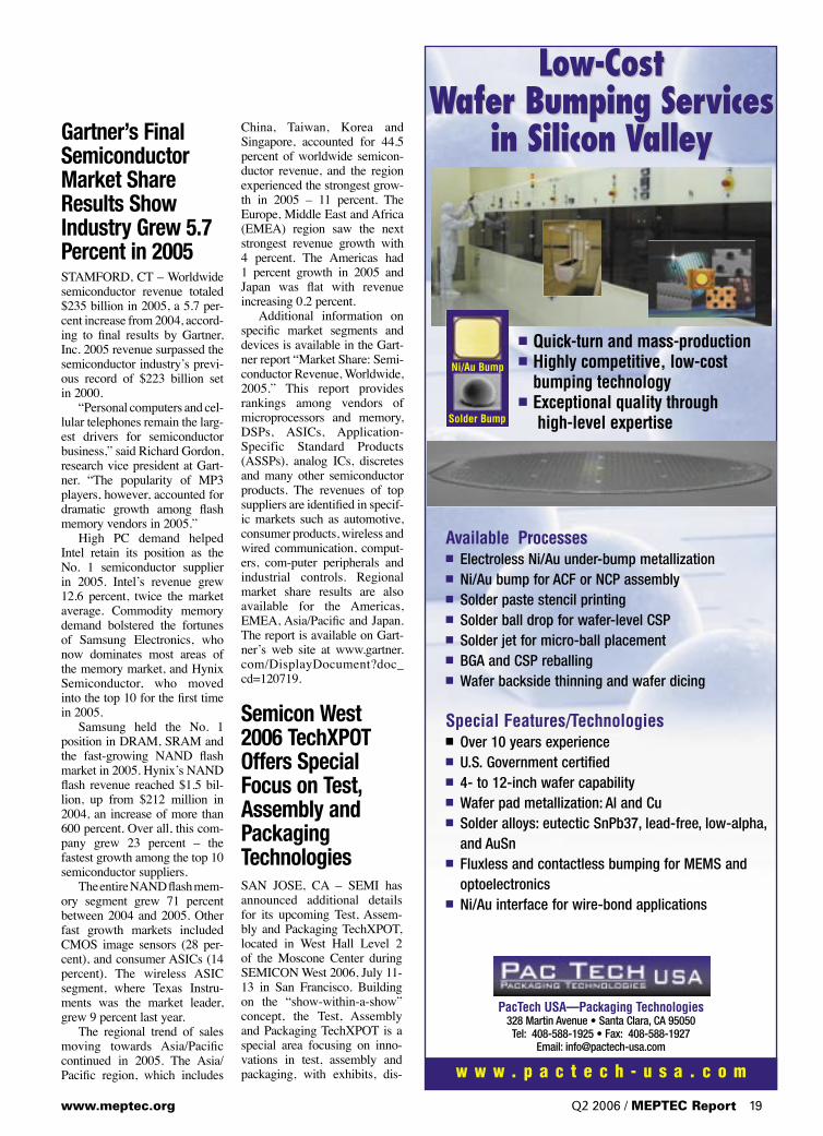
Low-CostWafer Bumping Services
in Silicon Valley
PacTech USA—Packaging Technologies328 Martin Avenue • Santa Clara, CA 95050Tel: 408-588-1925 • Fax: 408-588-1927
Email: [email protected]
w w w . p a c t e c h - u s a . c o m
Available Processes■ Electroless Ni/Au under-bump metallization ■ Ni/Au bump for ACF or NCP assembly■ Solder paste stencil printing■ Solder ball drop for wafer-level CSP■ Solder jet for micro-ball placement■ BGA and CSP reballing■ Wafer backside thinning and wafer dicing
Special Features/Technologies■ Over 10 years experience■ U.S. Government certified■ 4- to 12-inch wafer capability■ Wafer pad metallization: Al and Cu■ Solder alloys: eutectic SnPb37, lead-free, low-alpha, and AuSn■ Fluxless and contactless bumping for MEMS and optoelectronics■ Ni/Au interface for wire-bond applications
■ Quick-turn and mass-production■ Highly competitive, low-cost bumping technology■ Exceptional quality through high-level expertiseSolder Bump
Ni/Au Bump
Low-CostWafer Bumping Services
in Silicon Valley
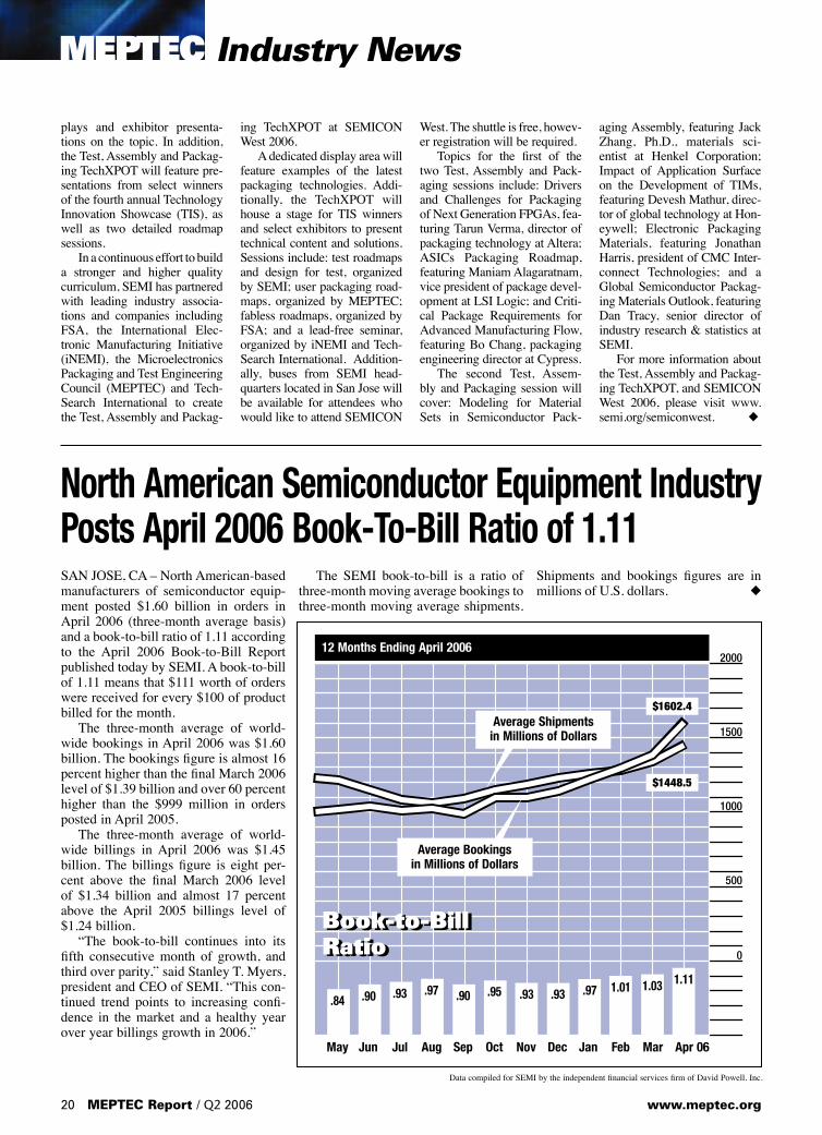
SAN JOSE, CA – North American-based manufacturers of semiconductor equip-ment posted $1.60 billion in orders in April 2006 (three-month average basis) and a book-to-bill ratio of 1.11 according to the April 2006 Book-to-Bill Report published today by SEMI. A book-to-bill of 1.11 means that $111 worth of orders were received for every $100 of product billed for the month. The three-month average of world-wide bookings in April 2006 was $1.60 billion. The bookings figure is almost 16 percent higher than the final March 2006 level of $1.39 billion and over 60 percent higher than the $999 million in orders posted in April 2005. The three-month average of world-wide billings in April 2006 was $1.45 billion. The billings figure is eight per-cent above the final March 2006 level of $1.34 billion and almost 17 percent above the April 2005 billings level of $1.24 billion. “The book-to-bill continues into its fifth consecutive month of growth, and third over parity,” said Stanley T. Myers, president and CEO of SEMI. “This con-tinued trend points to increasing confi-dence in the market and a healthy year over year billings growth in 2006.”
The SEMI book-to-bill is a ratio of three-month moving average bookings to three-month moving average shipments.
Shipments and bookings figures are in millions of U.S. dollars. ◆
Bar scale starts at 255 per increment
plays and exhibitor presenta-tions on the topic. In addition, the Test, Assembly and Packag-ing TechXPOT will feature pre-sentations from select winners of the fourth annual Technology Innovation Showcase (TIS), as well as two detailed roadmap sessions. In a continuous effort to build a stronger and higher quality curriculum, SEMI has partnered with leading industry associa-tions and companies including FSA, the International Elec-tronic Manufacturing Initiative (iNEMI), the Microelectronics Packaging and Test Engineering Council (MEPTEC) and Tech-Search International to create the Test, Assembly and Packag-
ing TechXPOT at SEMICON West 2006. A dedicated display area will feature examples of the latest packaging technologies. Addi-tionally, the TechXPOT will house a stage for TIS winners and select exhibitors to present technical content and solutions. Sessions include: test roadmaps and design for test, organized by SEMI; user packaging road-maps, organized by MEPTEC; fabless roadmaps, organized by FSA; and a lead-free seminar, organized by iNEMI and Tech-Search International. Addition-ally, buses from SEMI head-quarters located in San Jose will be available for attendees who would like to attend SEMICON
West. The shuttle is free, howev-er registration will be required. Topics for the first of the two Test, Assembly and Pack-aging sessions include: Drivers and Challenges for Packaging of Next Generation FPGAs, fea-turing Tarun Verma, director of packaging technology at Altera; ASICs Packaging Roadmap, featuring Maniam Alagaratnam, vice president of package devel-opment at LSI Logic; and Criti-cal Package Requirements for Advanced Manufacturing Flow, featuring Bo Chang, packaging engineering director at Cypress. The second Test, Assem-bly and Packaging session will cover: Modeling for Material Sets in Semiconductor Pack-
aging Assembly, featuring Jack Zhang, Ph.D., materials sci-entist at Henkel Corporation; Impact of Application Surface on the Development of TIMs, featuring Devesh Mathur, direc-tor of global technology at Hon-eywell; Electronic Packaging Materials, featuring Jonathan Harris, president of CMC Inter-connect Technologies; and a Global Semiconductor Packag-ing Materials Outlook, featuring Dan Tracy, senior director of industry research & statistics at SEMI. For more information about the Test, Assembly and Packag-ing TechXPOT, and SEMICON West 2006, please visit www.semi.org/semiconwest. ◆
20 MEPTEC Report / Q2 2006 www.meptec.org
North American Semiconductor Equipment Industry Posts April 2006 Book-To-Bill Ratio of 1.11
May Jun Jul Aug Sep Oct Nov Dec Jan Feb Mar Apr 06
$1448.5
12 Months Ending April 20062000
1500
500
0
1000
Data compiled for SEMI by the independent financial services firm of David Powell, Inc.
Average Shipmentsin Millions of Dollars
Average Bookingsin Millions of Dollars
$1602.4
MEPTEC Industry News
Book-to-Bill RatioBook-to-Bill Ratio
1.03 1.111.01
.90 .95.84 .90 .93 .97 .93 .97.93
© 2006 Semiconductor Equipment and Materials International (SEMI®). All rights reserved.
Expect the World.
Expect more than 1,300 of the world’s most innovative technology companiesshowcasing what’s next and what’s now for semiconductors, nanotechnology,MEMS, energy applications and more. If it’s out there, it’s here.
This is SEMICON® West.
REGISTER TODAYwww.semi.org/semiconwest
Moscone CenterSan Francisco, California
July 10–14 2006Event Dates: July 10–14
Exhibit Dates: July 11–13
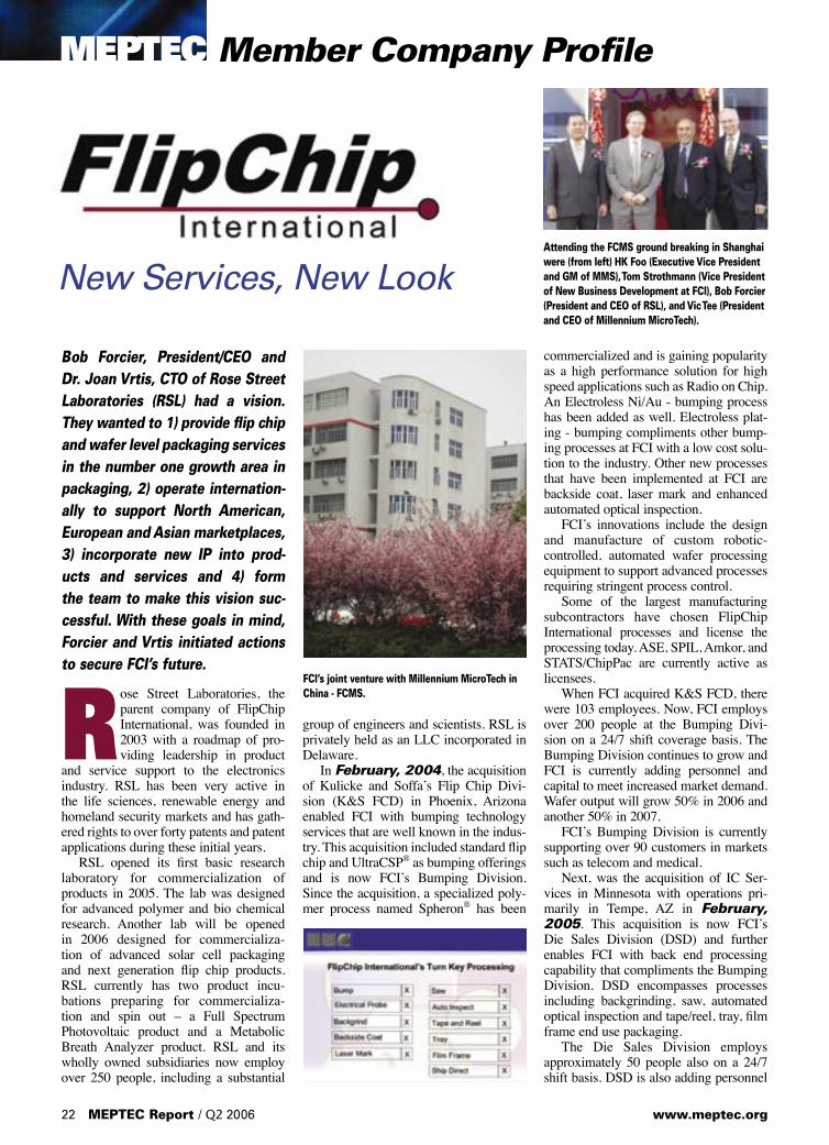
Bob Forcier, President/CEO and Dr. Joan Vrtis, CTO of Rose Street Laboratories (RSL) had a vision. They wanted to 1) provide flip chip and wafer level packaging services in the number one growth area in packaging, 2) operate internation-ally to support North American, European and Asian marketplaces, 3) incorporate new IP into prod-ucts and services and 4) form the team to make this vision suc-cessful. With these goals in mind, Forcier and Vrtis initiated actions to secure FCI’s future.
R ose Street Laboratories, the parent company of FlipChip International, was founded in 2003 with a roadmap of pro-viding leadership in product
and service support to the electronics industry. RSL has been very active in the life sciences, renewable energy and homeland security markets and has gath-ered rights to over forty patents and patent applications during these initial years. RSL opened its first basic research laboratory for commercialization of products in 2005. The lab was designed for advanced polymer and bio chemical research. Another lab will be opened in 2006 designed for commercializa-tion of advanced solar cell packaging and next generation flip chip products. RSL currently has two product incu-bations preparing for commercializa-tion and spin out – a Full Spectrum Photovoltaic product and a Metabolic Breath Analyzer product. RSL and its wholly owned subsidiaries now employ over 250 people, including a substantial
group of engineers and scientists. RSL is privately held as an LLC incorporated in Delaware. In February, 2004, the acquisition of Kulicke and Soffa’s Flip Chip Divi-sion (K&S FCD) in Phoenix, Arizona enabled FCI with bumping technology services that are well known in the indus-try. This acquisition included standard flip chip and UltraCSP® as bumping offerings and is now FCI’s Bumping Division. Since the acquisition, a specialized poly-mer process named Spheron® has been
commercialized and is gaining popularity as a high performance solution for high speed applications such as Radio on Chip. An Electroless Ni/Au - bumping process has been added as well. Electroless plat-ing - bumping compliments other bump-ing processes at FCI with a low cost solu-tion to the industry. Other new processes that have been implemented at FCI are backside coat, laser mark and enhanced automated optical inspection. FCI’s innovations include the design and manufacture of custom robotic- controlled, automated wafer processing equipment to support advanced processes requiring stringent process control. Some of the largest manufacturing subcontractors have chosen FlipChip International processes and license the processing today. ASE, SPIL, Amkor, and STATS/ChipPac are currently active as licensees. When FCI acquired K&S FCD, there were 103 employees. Now, FCI employs over 200 people at the Bumping Divi-sion on a 24/7 shift coverage basis. The Bumping Division continues to grow and FCI is currently adding personnel and capital to meet increased market demand. Wafer output will grow 50% in 2006 and another 50% in 2007. FCI’s Bumping Division is currently supporting over 90 customers in markets such as telecom and medical. Next, was the acquisition of IC Ser-vices in Minnesota with operations pri-marily in Tempe, AZ in February, 2005. This acquisition is now FCI’s Die Sales Division (DSD) and further enables FCI with back end processing capability that compliments the Bumping Division. DSD encompasses processes including backgrinding, saw, automated optical inspection and tape/reel, tray, film frame end use packaging. The Die Sales Division employs approximately 50 people also on a 24/7 shift basis. DSD is also adding personnel
MEPTEC Member Company Profile
22 MEPTEC Report / Q2 2006 www.meptec.org
New Services, New LookAttending the FCMS ground breaking in Shanghai were (from left) HK Foo (Executive Vice President and GM of MMS), Tom Strothmann (Vice President of New Business Development at FCI), Bob Forcier (President and CEO of RSL), and Vic Tee (President and CEO of Millennium MicroTech).
FCI’s joint venture with Millennium MicroTech in China - FCMS.
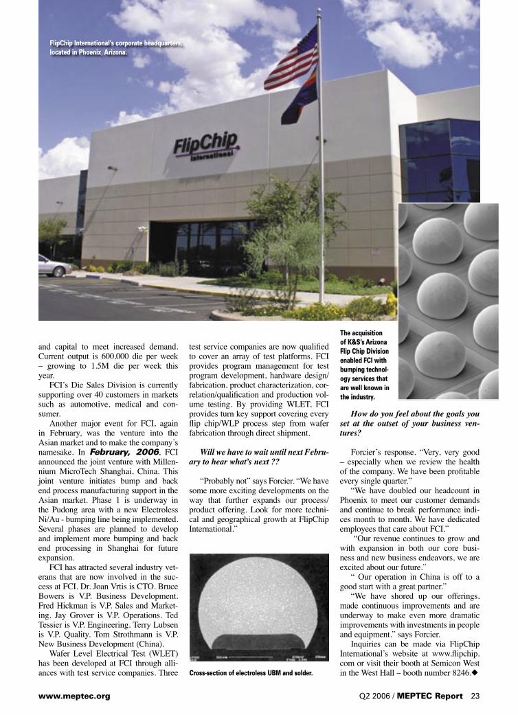
and capital to meet increased demand. Current output is 600,000 die per week – growing to 1.5M die per week this year. FCI’s Die Sales Division is currently supporting over 40 customers in markets such as automotive, medical and con-sumer. Another major event for FCI, again in February, was the venture into the Asian market and to make the company’s namesake. In February, 2006, FCI announced the joint venture with Millen-nium MicroTech Shanghai, China. This joint venture initiates bump and back end process manufacturing support in the Asian market. Phase 1 is underway in the Pudong area with a new Electroless Ni/Au - bumping line being implemented. Several phases are planned to develop and implement more bumping and back end processing in Shanghai for future expansion. FCI has attracted several industry vet-erans that are now involved in the suc-cess at FCI. Dr. Joan Vrtis is CTO. Bruce Bowers is V.P. Business Development. Fred Hickman is V.P. Sales and Market-ing. Jay Grover is V.P. Operations. Ted Tessier is V.P. Engineering. Terry Lubsen is V.P. Quality. Tom Strothmann is V.P. New Business Development (China). Wafer Level Electrical Test (WLET) has been developed at FCI through alli-ances with test service companies. Three
test service companies are now qualifi ed to cover an array of test platforms. FCI provides program management for test program development, hardware design/fabrication, product characterization, cor-relation/qualifi cation and production vol-ume testing. By providing WLET, FCI provides turn key support covering every fl ip chip/WLP process step from wafer fabrication through direct shipment.
Will we have to wait until next Febru-ary to hear what’s next ??
“Probably not” says Forcier. “We have some more exciting developments on the way that further expands our process/product offering. Look for more techni-cal and geographical growth at FlipChip International.”
How do you feel about the goals you set at the outset of your business ven-tures?
Forcier’s response. “Very, very good – especially when we review the health of the company. We have been profi table every single quarter.” “We have doubled our headcount in Phoenix to meet our customer demands and continue to break performance indi-ces month to month. We have dedicated employees that care about FCI.” “Our revenue continues to grow and with expansion in both our core busi-ness and new business endeavors, we are excited about our future.” “ Our operation in China is off to a good start with a great partner.” “We have shored up our offerings, made continuous improvements and are underway to make even more dramatic improvements with investments in people and equipment.” says Forcier. Inquiries can be made via FlipChip International’s website at www.fl ipchip.com or visit their booth at Semicon West in the West Hall – booth number 8246.◆
www.meptec.org Q2 2006 / MEPTEC Report 23
FlipChip International’s corporate headquarters, located in Phoenix, Arizona.
Cross-section of electroless UBM and solder.
The acquisition of K&S’s Arizona Flip Chip Division enabled FCI with bumping technol-ogy services that are well known in the industry.
T he fast growing market of handheld devices drives the miniaturization of components and subsystems. In addition to performance, package size and assembly strategy have
become key parameters. Chip scale pack-ages begin to replace traditional leadframe packages and device integration in subsys-tems is strongly emerging supported by wafer level packaging technology. Using silicon as a packaging material has advantages in thermal performance to support power dissipation of devices in high density assemblies, it matches the coefficient of thermal expansion (CTE) of silicon based devices like electronic ICs or micro-electro-mechanical systems (MEMS) and thus reduces thermo-mechanical stress and increases reliability. In this article we describe the use of micro-machined silicon with vertical through wafer µ-vias as a packaging plat-form. Vertical feed-throughs in silicon play a pivotal role to meet the stringent require-ments of handheld applications with respect to cost, size and manufacturability. In addi-tion monolithic integration of passives and precise mechanical manufacturing together with accurate alignment during wafer to wafer assembly allows for ultra small and low profile silicon packages.
Package Requirements To enable low cost, high volume pack-aging the complete manufacturing flow of components and systems has to be con-sidered. Size constrains of final products require subsystems with small footprint and low profile while the board level interface and the design rules defined by standard IC assembly processes constrain the I/O density of electrical interconnects. Device integration in one package reduces the num-ber of I/Os to board and enables complete subsystems. System designers prefer the use of com-pletely tested sub systems encouraging the development of systems in a package (SiP). Board level assembly requires surface
mount technology, and the packages need to interface with solder land pads or solder bumped pads. Conventional packages use die level handling with complex, and costly pro-cesses. For MEMS devices the particle generation during assembly can result in failure of the device and 2nd level packag-ing contributes to the large device size. A significant portion of up to 70% of the final device cost originates in the packaging of the component. The advantage of wafer level packag-ing compared to individual die handling explains the increasing popularity of this process. This includes chip to wafer assem-bly of active and passive components and sealing caps on wafer level by the use of pick and place equipment. In addition wafer to wafer sealing or stacking of two or more wafers has become an enabling technol-ogy. The wafer level processes completely changes the cost structure of the final pack-age by reducing die handling, shortened alignment cycles and decreased bill of mate-rial. Hermetic sealing of devices is an addi-tional requirement mainly known from the MEMS world. Different sealing methods are available and care must be taken that
the selected process is compatible with the MEMS device. Surface to surface bonding, like anodic or fusion bonding, involves high tempera-tures and require a flat surface. An alterna-tive sometimes used is surface activation at low temperature. Like the methods previ-ously outlines, this has the disadvantage that it does not provide electrical connec-tion to the device. Commonly used in the MEMS industry is glass frit sealing. This insulating interlayer needs a wide sealing ring to provide reliable sealing and lateral electrical feed-throughs increase the space requirement on the MEMS device. A metal-lic interlayer on the other hand allows for narrow sealing rings and small footprint when vertical electrical feed-throughs are available.
HyCap® - The Silicon Packaging Solution Hymite has developed and manufac-tures silicon packages utilizing vertical, hermetic feed-throughs. A representative package is shown schematically in Figure 1 with a MEMS device hermetically sealed
MEPTEC Silicon Packaging Technology
Low Cost, High Performance Silicon PackagesVertical µ-via enabled silicon wafer level packaging for hermetic sealing, stacking and SiP applicationsDr. Jochen Kuhmann, CTO, Andreas Hase, Product ManagerHymite A/S, Denmark, Hymite GmbH, Germany
24 MEPTEC Report / Q2 2006 www.meptec.org
Figure 1: Schematic of MEMS packaging by HyCap®. HyCap® provides sealing and electrical connection to MEMS in a one step assembly. Electrical µ-vias enable smaller MEMS and SMT mounting to a carrier or PCB board. Insert: mi-croscope picture of a cross sectioning through a µ-via.
Figure 2: HyCap®S wafer with enlarged pictures of the sealing ring side and the SMT side. Elec-troplated AuSn solder on the electrical connec-tion and sealing ring metallization defines the interface to MEMS device. The deep cavity of up to 500 µm gives headroom for devices. The SMT side shows pads for solder deposition by stencil printing separated by a solder dam.
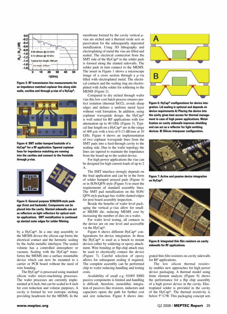
by a HyCap®. In a one step assembly to the MEMS device the silicon cap forms the electrical contact and the hermetic sealing by the AuSn metallic interlayer. The sealed volume has a controlled atmosphere or vacuum. Sealing with the HyCap® trans-forms the MEMS into a surface mountable device which can now be mounted to a carrier or PCB board without the need of wire bonding. The HyCap® is processed using standard silicon wafer micro-machining processes. The wafer processes are currently imple-mented at 6 inch, but can be scaled to 8 inch for cost reduction and volume purposes. A cavity is formed by wet isotropic etching providing headroom for the MEMS. In the
membrane formed by the cavity vertical µ-vias are etched and a thermal oxide acts as passivation for the subsequently deposited metallization. Using 3D lithography and electroplating of metal the vias are filled and sealed. The electrical connection from the SMT side of the HyCap® to the solder pads is formed along the slanted sidewalls. The solder pads in turn connect to the MEMS. The insert in Figure 1 shows a microscope image of a cross section through a µ-via filled with electroplated metal. The electri-cal contacts and the sealing ring are electro-plated with AuSn solder for soldering to the MEMS (Figure 2). Compared to dry etched through wafer vias this low cost batch process ensures per-fect isolation (thermal SiO2), avoids sharp edges and defines a uniform metal layer without void formation. In addition, using coplanar waveguide design, the HyCap® is well suited for RF applications with low attenuation up to 40 GHz (Figure 3). Typi-cal line length on a HyCap® are in the range of 400 µm with a loss of 0.13 dB/mm at 10 GHz. Figure 4 shows an implementation of two coplanar waveguide lines from the SMT pads into a feed-through cavity to the sealing side. Due to the wafer topology the lines are tapered to maintain the impedance from the board up to the sealed device. For high power applications the vias can be designed for high current loads of up to 2 A. The SMT interface strongly depends on the final application and can be in the form of solder bumped arrayed pads (Figure 4) or in SON/QFN style (Figure 5) to meet the requirements of standard assembly lines. The SMT pad metallization on the SON/QFN style package has visible slanted edges for post board assembly inspection. Beside the benefits of wafer level pack-aging the vertical µ-vias allow for small-er MEMS die, reducing MEMS cost by increasing the number of dies on a wafer. For wafer level testing, all contacts to the device are on one level and accessible via the HyCap®. Figure 6 shows different HyCap® con-figurations for device integration. In these the HyCap® is used as a bench to mount devices either by soldering or epoxy attach-ment. Wire bonding or flip-chip attach may be used to electrically contact the device (Figure 7). Careful selection of epoxy allows for subsequent sealing if required. The complete assembly can be performed chip to wafer reducing handling and testing costs. Availability of small e.g. 01005 SMD passive components is limited and handling is difficult, therefore, monolithic integra-tion of passives like resistors, inductors and capacitors opens the path for further cost and size reduction. Figure 8 shows inte-
grated thin film resistors on cavity sidewalls for RF applications. The low silicon thermal resistiv-ity enables new approaches for high power device packaging. A thermal model using finite element analysis (Figure 9) shows the performance for a flip chip assembly of a high power device in the cavity. Elec-troplated solder is provided in the cavity of the HyCap®. The thermal resistivity is below 5° C/W. This packaging concept sets
Figure 3: RF transmission line measurements for an impedance matched coplanar line along side-walls, cavities and through µ-vias of a HyCap®.
Figure 5: General purpose SON/QFN-style pack-age (front and backside). Components can be placed into the cavity. Slanted sidewalls can act as reflectors as light reflectors for optical emit-ter applications. SMT metallization is continued up slanted outer edges for solder filleting.
Figure 4: SMT solder bumped backside of a HyCap® for a RF application. Tapered coplanar lines for impedance matching are running into the cavities and connect to the frontside through µ-vias.
www.meptec.org Q2 2006 / MEPTEC Report 25
Figure 8: Integrated thin film resistors on cavity sidewalls for RF applications.
Figure 7: Active and passive device integration on HyCap®.
Figure 6: HyCap® configurations for device inte-gration. Lid sealing is optional and depends on device requirements A) Placing the device into the cavity gives best access for thermal manage-ment in case of high power applications. Metal-lization on cavity sidewalls improves shielding and can act as a reflector for light emitting devices. B) Silicon interposer configuration.
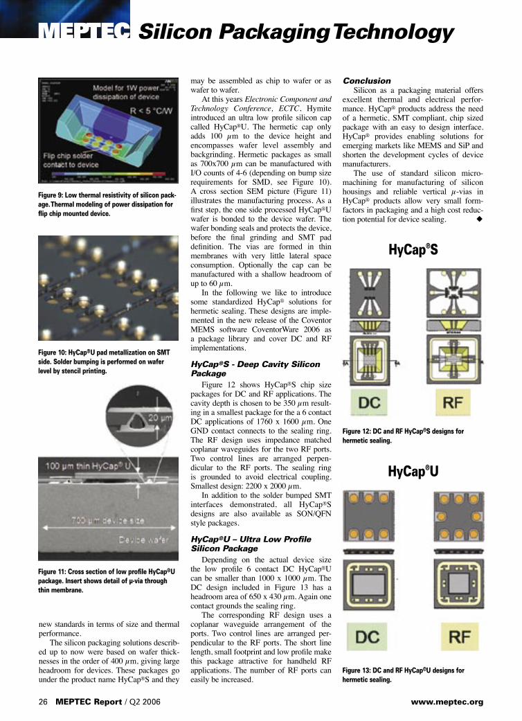
new standards in terms of size and thermal performance. The silicon packaging solutions describ-ed up to now were based on wafer thick-nesses in the order of 400 µm, giving large headroom for devices. These packages go under the product name HyCap®S and they
may be assembled as chip to wafer or as wafer to wafer. At this years Electronic Component and Technology Conference, ECTC, Hymite introduced an ultra low profile silicon cap called HyCap®U. The hermetic cap only adds 100 µm to the device height and encompasses wafer level assembly and backgrinding. Hermetic packages as small as 700x700 µm can be manufactured with I/O counts of 4-6 (depending on bump size requirements for SMD, see Figure 10). A cross section SEM picture (Figure 11) illustrates the manufacturing process. As a first step, the one side processed HyCap®U wafer is bonded to the device wafer. The wafer bonding seals and protects the device, before the final grinding and SMT pad definition. The vias are formed in thin membranes with very little lateral space consumption. Optionally the cap can be manufactured with a shallow headroom of up to 60 µm. In the following we like to introduce some standardized HyCap® solutions for hermetic sealing. These designs are imple-mented in the new release of the Coventor MEMS software CoventorWare 2006 as a package library and cover DC and RF implementations.
HyCap®S - Deep Cavity Silicon Package Figure 12 shows HyCap®S chip size packages for DC and RF applications. The cavity depth is chosen to be 350 µm result-ing in a smallest package for the a 6 contact DC applications of 1760 x 1600 µm. One GND contact connects to the sealing ring. The RF design uses impedance matched coplanar waveguides for the two RF ports. Two control lines are arranged perpen-dicular to the RF ports. The sealing ring is grounded to avoid electrical coupling. Smallest design: 2200 x 2000 µm. In addition to the solder bumped SMT interfaces demonstrated, all HyCap®S designs are also available as SON/QFN style packages.
HyCap®U – Ultra Low Profile Silicon Package Depending on the actual device size the low profile 6 contact DC HyCap®U can be smaller than 1000 x 1000 µm. The DC design included in Figure 13 has a headroom area of 650 x 430 µm. Again one contact grounds the sealing ring. The corresponding RF design uses a coplanar waveguide arrangement of the ports. Two control lines are arranged per-pendicular to the RF ports. The short line length, small footprint and low profile make this package attractive for handheld RF applications. The number of RF ports can easily be increased.
Conclusion Silicon as a packaging material offers excellent thermal and electrical perfor-mance. HyCap® products address the need of a hermetic, SMT compliant, chip sized package with an easy to design interface. HyCap® provides enabling solutions for emerging markets like MEMS and SiP and shorten the development cycles of device manufacturers. The use of standard silicon micro-machining for manufacturing of silicon housings and reliable vertical µ-vias in HyCap® products allow very small form-factors in packaging and a high cost reduc-tion potential for device sealing. ◆
MEPTEC Silicon Packaging Technology
26 MEPTEC Report / Q2 2006 www.meptec.org
Figure 10: HyCap®U pad metallization on SMT side. Solder bumping is performed on wafer level by stencil printing.
Figure 11: Cross section of low profile HyCap®U package. Insert shows detail of µ-via through thin membrane.
Figure 9: Low thermal resistivity of silicon pack-age. Thermal modeling of power dissipation for flip chip mounted device.
Figure 13: DC and RF HyCap®U designs for hermetic sealing.
HyCap®U
Figure 12: DC and RF HyCap®S designs for hermetic sealing.
HyCap®S

Introducing Hyatt’s new Grand Bed, ultra-plush pillows, the softest of sheeting, and a thick down blanket — all piled atop an irresistible pillow-top mattress. The Grand Bed, found exclusively at select Hyatt Hotels and Resorts. Beginning January 1, 2006. This is not your typical hotel story. This is the Hyatt Touch.TM For more information, call 408 993 1234 or visit hyattsanjose.hyatt.com.
INTRODUCING HYATT SAN JOSE’S NEW GRAND BED.TM©
2005
Hya
tt Co
rp.
EDEL PARTNERS Quark 6.0 Trim: 7.875 ins. x 10.875 ins. Constructed At: 100% Output At:100%PUB: MEPTEC Inks Used: CMYK Team: mky Proof: 1Date 12/15/05 Page 1 of 1 Preflighted 0/0/00 Fonts Used Uni ers A enir Hel etica Cond
SJO21009.01.a_AdResize.qxd 12/21/05 2:31 PM Page 1
Materials Declarations for Everyone N. Nagaraj, PhD, PEPapros Inc.
C urrent and potential future regula-tions have brought about a need for a uniform and consistent meth-od for encapturing, expressing and exchanging material content
data in the form of Material Composition Declarations. Materials Declarations may be exchanged in a variety of means. These can be distributed on secure websites, exchanged securely such as by using the IPC forms 1752 or by traditional less secure email, flash drives or other modes of storage. Supply chain data requires high degrees of security, and thus reduces the choices frequently to distribution on secure websites or for exchange of the IPC 1752 forms. The need for exchange of IPC 1752 form information requires companies to generate accurate material composition infor-mation that the users can rely on to generate their own MCDs.
Discussion Users of Material Declarations for parts and/or products can obtain MCDs downloaded from a secure website if they are distrib-uted as such. Typically, Material Declarations exchanges can occur by a Requester sending a request in an IPC form electronically to a Supplier. This Supplier captures the requester information including any custom declara-tions and/or other details and collates it with requested information and sends it back in the IPC 1752 electronic form. In the context of the diagram, the term Supplier is used to mean either the Supplier who is collecting Product information for the manufacturer or the manu-facturer who is supplying all of the product information. The manufacturer him/herself could in other contexts be a requester when requesting MCDs for parts procured. In fact in the figure, that is one of the methods that the Supplier collects information such as shown in the bottom left of the “Supplier tasks” box. The Supplier/Manufacturer should be able to read in easily parts data from IPC 1752 forms, do a BOM merge, account for parts not in BOM (solder, wire, cable etc, if any), add in desktop engineering calculations that are permitted by the industry standards on a layerwise basis, test all other parts layerwise and do a final merge of all of this for any product material declara-tion. The following figure shows the potential flow of data associated with requests for, replies to, compilation of, and distribution of material composition information. This information flow
can extend from any point in the supply chain to any other. Small manufacturers can request parts information from major manufacturers that they use for making their own products. Similarly, large manufacturers can request this information from small or medium manufac-turers for compilation of products comprised of many small assemblies. The point of inter-est is that using the IPC 1752 form creates a platform that can satisfy the needs for all of these exchanges in a smooth, seamless and speedy manner. The underlying xml schema associated with the IPC 1752 form is enables exchange of information using the open for-mat for data interchange, the xml (Extensible Markup Language) format. The xml format, in addition to being non-proprietary, also enables data to be stored fairly efficiently in a manner that several applications can access it. It is important to recognize that material information must be calculated on a part-level basis and also at the homogeneous layer level. The latter need is to satisfy the RoHS stan-dards. Desktop engineering calculations allowed by the standards must be entered as informa-tion on a layerwise basis. This is true for test data also. These must be automated to read from text or spreadsheet files to reduce input errors Typically, desktop engineering data and test data are both entered in a speciated form (each substance referenced by its CAS). How-ever, MCDs in the IPC 1752 forms will be listed in categories. The supplier/manufacturer must be able to integrate all of this informa-tion as well as BOM information for each of these parts in the computing process. The Supplier/Manufacturer obviously does not do this for every request, but has a library where
such information is stored once the MCD is computed the first time. From here the Sup-plier/Manufacturer merges this with Requester information captured just earlier, and can any time reply with full product information. The Supplier/Manufacturer can also just directly distribute or respond to requester using a standard distribution form. He/She can also send requester a standard email to discourage spam activities, if situation necessitates this. The libraries of the Supplier/Manufacturer, in addition to being used to distribute material information, must also account for parts infor-mation inequities. Pre-RoHS and post-RoHS parts might in common cases, contain the same part number. Also, the same part supplied by a different supplier might often possess a differ-ent MCD. Easy access for such information necessitates associating this with the proper file for the part MCD. All this information can be easily stored in the form of a name for the file that the information is stored in. For example a part of part number xyz, when suffixed a sup-plier id, which could be a real id, or in the case of pre-RoHS and post RoHS part sharing the same part number, an id that references this, becomes xyz-1.xml. The suffix 1 could refer to the supplier ID or a reference to distinguish parts having shared part numbers. This enables data to be thus kept natively in xml and accessed only as needed. This enables easy exchange of data with external applications, if need be. Parts information, which is read from engi-neering calculations or test data, could also be kept in such form after appropriate aggrega-tion of individual layer information. Obvi-ously, such aggregation includes summation of all substance masses in the category and
MEPTEC Materials Technology
28 MEPTEC Report / Q2 2006 www.meptec.org
also identifi cation of the layer containing the maximum concentration and the value of the maximum concentration for RoHS purposes. In keeping parts data simply as xml fi les in an IPC 1752 format can have several other advantages. Typically, each xml fi le may be of only 20 kilobytes in size. Without the need for any database to store in, xml fi les for a million parts, comprising approximately less than 25 gigabytes, can be quite easily kept on a single desktop computer, with proper backups and archival as needed. As each xml fi le is accessed only as needed, there will be minimal slowdown of the program even if data is accessed in typically hierarchical data access applications such as spreadsheets as opposed to using relational databases (and, if any, IT or personnel overhead associated with that). Such an approach maintains the robustness associ-ated with high-end applications, while at the same time it allows for economical implemen-tation of the MCD process and its associated tasks. Management and maintenance of data is also thus easier because the requirements for personnel to maintain data and systems are less stringent, requiring only spreadsheet level expertise. This means that that the only exper-tise required for personnel to operate such a system would be related to materials, parts and inventories. Other preferable options in developing MCDs are that the user should be able to view all compositions, maximum concentrations and the associated layer information for the layer containing the maximum concentration prior to creating the IPC 1752 form. This is because the user may want to add additional identifying or explanatory information relat-ing to the layer or the material used. Typical spreadsheet applications could also be color coded to identify non-compliant layers thus enabling the user to reject such parts at an early stage. Training and personnel related issues also play a part in the MCD process. Turnover of personnel is quite common in the electronic manufacturing sector. So the MCD process should be enabled to allow for easy transition of new personnel, who should be able to adapt to the job easily. This will keep the process of developing and exchanging of MCDs smooth and without kinks that can upset critical factors such as time-to-market. Adapting to Engineering Change Orders (ECO) will also be easy in such an approach. With MCDs being able to be generated eas-ily, ECO implementation will be made easier. Alternate parts information from different sup-pliers capable of fulfi lling the ECO can be eas-ily evaluated by quickly preparing MCDs and evaluating compliance. This will enable the ECO to be implemented with lesser cost over-heads and maximize profi ts for companies.
SummaryThese best management practices for supply chain data using the IPC form 1752 enable a smooth, uniform and consistent exchange of data at any point or layer or link of the supply chain. ◆
www.meptec.org Q2 2006 / MEPTEC Report 29
��������������������������������������������������������
����������������������������
����������������������������������������������������������������������������������������������������������������������������������������������������������������������������������
������������������������������������������
�����������������������������������������������������
����������������������������������������������������������
������������������������������������������������������������������������������������
Wire
Washers
Squares
Frames
Foil
Spheres
Paste
CustomShapes
■ Pure indium for low temperature sealing
■ Indium alloys for step soldering and thermal interfacing
■ AuSn alloys for fl uxless die-attach and hermetic packaging
Tech Fact:Indium metal is highly workable, provides excellent hermeticity, and can be processed at low temperatures.
For competitively priced, on-time solutions:
Send Us Your RFQ:[email protected]
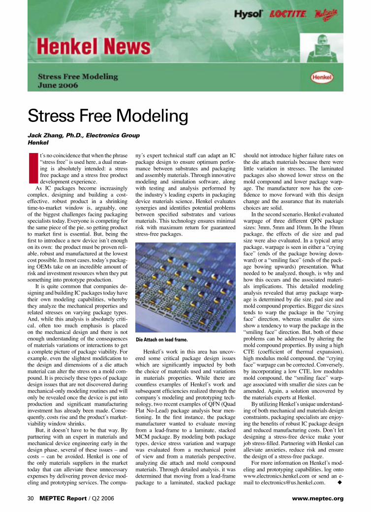
It’s no coincidence that when the phrase “stress free” is used here, a dual mean-ing is absolutely intended: a stress free package and a stress free product development experience.
As IC packages become increasingly complex, designing and building a cost-effective, robust product in a shrinking time-to-market window is, arguably, one of the biggest challenges facing packaging specialists today. Everyone is competing for the same piece of the pie, so getting product to market first is essential. But, being the first to introduce a new device isn’t enough on its own: the product must be proven reli-able, robust and manufactured at the lowest cost possible. In most cases, today’s packag-ing OEMs take on an incredible amount of risk and investment resources when they put something into prototype production. It is quite common that companies de-signing and building IC packages today have their own modeling capabilities, whereby they analyze the mechanical properties and related stresses on varying package types. And, while this analysis is absolutely criti-cal, often too much emphasis is placed on the mechanical design and there is not enough understanding of the consequences of materials variations or interactions to get a complete picture of package viability. For example, even the slightest modification to the design and dimensions of a die attach material can alter the stress on a mold com-pound. It is precisely these types of package design issues that are not discovered during mechanical-only modeling routines and will only be revealed once the device is put into production and significant manufacturing investment has already been made. Conse-quently, costs rise and the product’s market-viability window shrinks. But, it doesn’t have to be that way. By partnering with an expert in materials and mechanical device engineering early in the design phase, several of these issues – and costs – can be avoided. Henkel is one of the only materials suppliers in the market today that can alleviate these unnecessary expenses by delivering proven device mod-eling and prototyping services. The compa-
ny’s expert technical staff can adapt an IC package design to ensure optimum perfor-mance between substrates and packaging and assembly materials. Through innovative modeling and simulation software, along with testing and analysis performed by the industry’s leading experts in packaging device materials science, Henkel evaluates synergies and identifies potential problems between specified substrates and various materials. This technology ensures minimal risk with maximum return for guaranteed stress-free packages.
Henkel’s work in this area has uncov-ered some critical package design issues which are significantly impacted by both the choice of materials used and variations in materials properties. While there are countless examples of Henkel’s work and subsequent efficiencies realized through the company’s modeling and prototyping tech-nology, two recent examples of QFN (Quad Flat No-Lead) package analysis bear men-tioning. In the first instance, the package manufacturer wanted to evaluate moving from a lead-frame to a laminate, stacked MCM package. By modeling both package types, device stress variation and warpage was evaluated from a mechanical point of view and from a materials perspective, analyzing die attach and mold compound materials. Through detailed analysis, it was determined that moving from a lead-frame package to a laminated, stacked package
should not introduce higher failure rates on the die attach materials because there were little variation in stresses. The laminated packages also showed lower stress on the mold compound and lower package warp-age. The manufacturer now has the con-fidence to move forward with this design change and the assurance that its materials choices are solid. In the second scenario, Henkel evaluated warpage of three different QFN package sizes: 3mm, 5mm and 10mm. In the 10mm package, the effects of die size and pad size were also evaluated. In a typical array package, warpage is seen in either a “crying face” (ends of the package bowing down-ward) or a “smiling face” (ends of the pack-age bowing upwards) presentation. What needed to be analyzed, though, is why and how this occurs and the associated materi-als implications. This detailed modeling analysis revealed that array package warp-age is determined by die size, pad size and mold compound properties. Bigger die sizes tends to warp the package in the “crying face” direction, whereas smaller die sizes show a tendency to warp the package in the “smiling face” direction. But, both of these problems can be addressed by altering the mold compound properties. By using a high CTE (coefficient of thermal expansion), high modulus mold compound, the “crying face” warpage can be corrected. Conversely, by incorporating a low CTE, low modulus mold compound, the “smiling face” warp-age associated with smaller die sizes can be amended. Again, a solution uncovered by the materials experts at Henkel. By utilizing Henkel’s unique understand-ing of both mechanical and materials design constraints, packaging specialists are enjoy-ing the benefits of robust IC package design and reduced manufacturing costs. Don’t let designing a stress-free device make your job stress-filled. Partnering with Henkel can alleviate anxieties, reduce risk and ensure the design of a stress-free package. For more information on Henkel’s mod-eling and prototyping capabilities, log onto www.electronics.henkel.com or send an e-mail to [email protected]. ◆
Die Attach on lead frame.
30 MEPTEC Report / Q2 2006 www.meptec.org
Stress Free ModelingJack Zhang, Ph.D., Electronics GroupHenkel

Henkel Americas: +1 949 789 2500 Henkel Europe: +44 1442 278 000 Henkel Asia: +852 2233 0000 electronics.henkel.com
“So much to do, so little time” is a common dilemma for today’s manufacturers. But, it neednot be this way. Henkel’s material sets will save you time for more pressing concerns.
Can you really afford to spend the time necessary toqualify, test and guarantee compatible products? If not,mistakes are inevitable. Fortunately, Henkel’s MaterialSets solve this dilemma by delivering proven packageperformance - stress reduction, compatible chemistryand material interface designs. Using the cross-quali-
fied Hysol mold compounds, QMI die attach adhesiveand underfills, this complete solution saves you upfront design time and reduces overall maintenancetime and costs. And you get the support of a world-renowned electronics specialist – Henkel is the Singlematerial solutions provider you’ve been waiting for.
Not enough hours in the day?Henkel’s material sets let you get back to more ‘important’ office work.
MEPTEC_CHAIR_FEB_resized 14/3/06 11:00 am Page 1
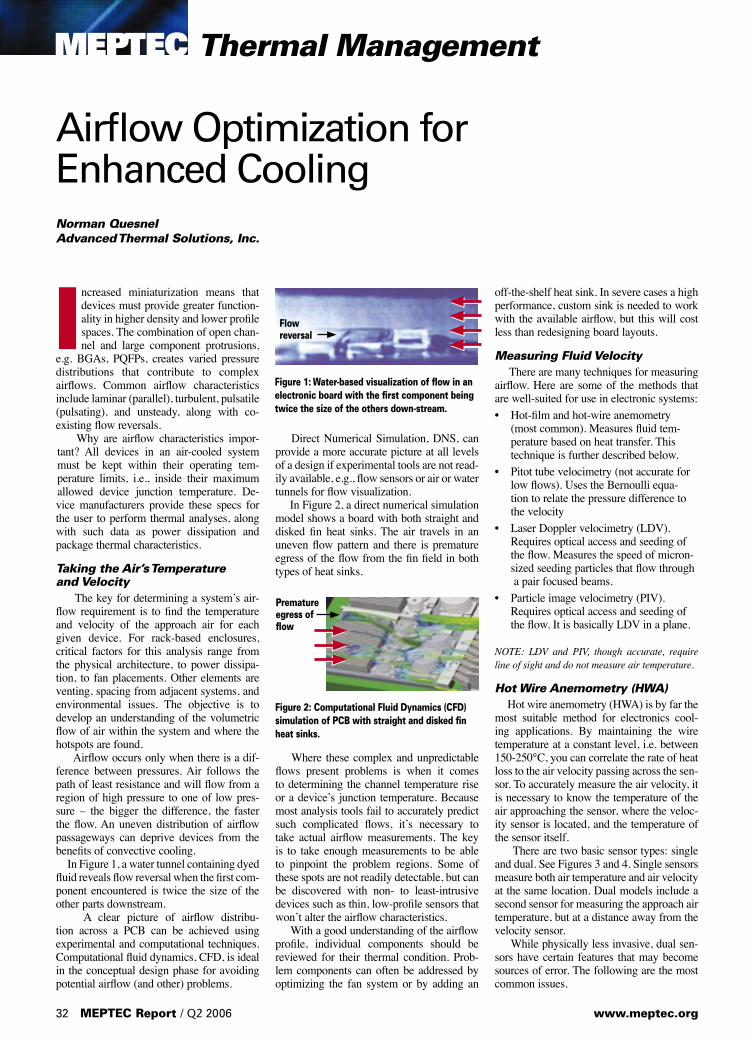
I ncreased miniaturization means that devices must provide greater function-ality in higher density and lower profile spaces. The combination of open chan-nel and large component protrusions,
e.g. BGAs, PQFPs, creates varied pressure distributions that contribute to complex airflows. Common airflow characteristics include laminar (parallel), turbulent, pulsatile (pulsating), and unsteady, along with co-existing flow reversals.
Why are airflow characteristics impor-tant? All devices in an air-cooled system must be kept within their operating tem-perature limits, i.e., inside their maximum allowed device junction temperature. De-vice manufacturers provide these specs for the user to perform thermal analyses, along with such data as power dissipation and package thermal characteristics. Taking the Air’s Temperature and Velocity The key for determining a system’s air-flow requirement is to find the temperature and velocity of the approach air for each given device. For rack-based enclosures, critical factors for this analysis range from the physical architecture, to power dissipa-tion, to fan placements. Other elements are venting, spacing from adjacent systems, and environmental issues. The objective is to develop an understanding of the volumetric flow of air within the system and where the hotspots are found. Airflow occurs only when there is a dif-ference between pressures. Air follows the path of least resistance and will flow from a region of high pressure to one of low pres-sure – the bigger the difference, the faster the flow. An uneven distribution of airflow passageways can deprive devices from the benefits of convective cooling. In Figure 1, a water tunnel containing dyed fluid reveals flow reversal when the first com-ponent encountered is twice the size of the other parts downstream. A clear picture of airflow distribu-tion across a PCB can be achieved using experimental and computational techniques. Computational fluid dynamics, CFD, is ideal in the conceptual design phase for avoiding potential airflow (and other) problems.
Direct Numerical Simulation, DNS, can provide a more accurate picture at all levels of a design if experimental tools are not read-ily available, e.g., flow sensors or air or water tunnels for flow visualization. In Figure 2, a direct numerical simulation model shows a board with both straight and disked fin heat sinks. The air travels in an uneven flow pattern and there is premature egress of the flow from the fin field in both types of heat sinks.
Where these complex and unpredictable flows present problems is when it comes to determining the channel temperature rise or a device’s junction temperature. Because most analysis tools fail to accurately predict such complicated flows, it’s necessary to take actual airflow measurements. The key is to take enough measurements to be able to pinpoint the problem regions. Some of these spots are not readily detectable, but can be discovered with non- to least-intrusive devices such as thin, low-profile sensors that won’t alter the airflow characteristics. With a good understanding of the airflow profile, individual components should be reviewed for their thermal condition. Prob-lem components can often be addressed by optimizing the fan system or by adding an
off-the-shelf heat sink. In severe cases a high performance, custom sink is needed to work with the available airflow, but this will cost less than redesigning board layouts.
Measuring Fluid Velocity There are many techniques for measuring airflow. Here are some of the methods that are well-suited for use in electronic systems:• Hot-film and hot-wire anemometry (most common). Measures fluid tem- perature based on heat transfer. This technique is further described below.• Pitot tube velocimetry (not accurate for low flows). Uses the Bernoulli equa- tion to relate the pressure difference to the velocity • Laser Doppler velocimetry (LDV). Requires optical access and seeding of the flow. Measures the speed of micron- sized seeding particles that flow through a pair focused beams. • Particle image velocimetry (PIV). Requires optical access and seeding of the flow. It is basically LDV in a plane.
NOTE: LDV and PIV, though accurate, require line of sight and do not measure air temperature.
Hot Wire Anemometry (HWA) Hot wire anemometry (HWA) is by far the most suitable method for electronics cool-ing applications. By maintaining the wire temperature at a constant level, i.e. between 150-250°C, you can correlate the rate of heat loss to the air velocity passing across the sen-sor. To accurately measure the air velocity, it is necessary to know the temperature of the air approaching the sensor, where the veloc-ity sensor is located, and the temperature of the sensor itself. There are two basic sensor types: single and dual. See Figures 3 and 4. Single sensors measure both air temperature and air velocity at the same location. Dual models include a second sensor for measuring the approach air temperature, but at a distance away from the velocity sensor. While physically less invasive, dual sen-sors have certain features that may become sources of error. The following are the most common issues.
Figure 1: Water-based visualization of flow in an electronic board with the first component being twice the size of the others down-stream.
Flowreversal
MEPTEC Thermal Management
Airflow Optimization for Enhanced CoolingNorman QuesnelAdvanced Thermal Solutions, Inc.
32 MEPTEC Report / Q2 2006 www.meptec.org
Figure 2: Computational Fluid Dynamics (CFD) simulation of PCB with straight and disked fin heat sinks.
Premature egress of flow
maxiGRIP TM
Ultimate Heat Sink Attachment System is
the new clip-on mounting method for fast, safe, and secure heat sink mounting
● ● ● ● ● No sink threading, cracked dies or detached components● ● ● ● ● Extended cooling surface
● ● ● ● ● Easy heat sink removal and re-attachment
Advanced Thermal Solutions, Inc.w w w . q a t s . c o m
© All Rights Reserved
Innovation in Thermal ManagmentTM
Clip N CoolThe easy and reliable cooling solution
‘
Fluid Temperature Gradient Due to the non-isothermal nature of airflow in electronic enclosures, dual sen-sors used for measuring temperature and air velocity at two different points can cause significant errors, particularly as values increase.
Radiated Heat Transfer Dual sensors contain both hot (veloc-ity) and cold (temperature) areas. Radiation coupling between the two will cause the temperature sensor to report a Ta value that is substantially larger than the actual. As a result, the measurement system will produce significant errors in air velocity magnitude.
Lack of Calibration at Elevated Temperature Because HWA is a heat transfer sensor, and is exposed to high temperature air during actual testing, calibration must include the impact of air temperature at different levels. Not having such calibration, there will be measurement errors.
Sensor Size and Its Support Body Good measurement practices mandate that the best sensor is the one that introduces the least disturbance in the flow field. Large blocks alter the flow dramatically and cause errors in measurement.
Conclusion A variety of thermal management issues can be solved using multipoint air velocity measurements. Typical uses include evaluat-ing the performance of fans and heat sinks. Another use is to verify CFD software mod-eling. Multipoint measurements have been used to profile printed circuit boards to determine critical component placement and to monitor quality. The best place to address thermal problems is in the concept stage where they are relatively cheap to fix. Other-wise, the cost for failing the eventual thermal tests will be much higher in terms of price and time. ◆
www.meptec.org Q1 2006 / MEPTEC Report 27
Figure 3: Single sensor technology. (Product of Advanced Thermal Solutions, Inc.)
Figure 4: Dual sensor technology.
NOW! 300mm WAFER DICING
CORWIL is the leader in wafer backgrinding, wafer dicing and visual inspection to commercial, military and medical specs. CORWIL’s newest addition in dicing equipment is a fully automatic, latest state-of-the-art 12 inch dicing saw that strengthens CORWIL’s technical leadership for chip-free and fast turn-around dicing. CORWIL dices Si, GaAs, Sapphire, SiGe, laminates and many other materials and CORWIL is unsur-passed in IC assembly in ceramic, BGA, flip-chip, and MLF/QFN type packages.• High Volume – millions of dice per month.• Automatic High-Speed Pick & Place• Automatic Vision Inspection Systems • Low K, MEMS and Optical/Imaging wafers processed• Experts in Multi-die Type Wafer dicing • Highest Quality and Best Service in the Industry
Since 1990 CORWIL has built its reputation providing customers with:
Excellent Quality and Superior ServicePhone 408-321-6404 • Fax 408-321-6407
www.corwil.com
34 MEPTEC Report / Q2 2006 www.meptec.org
MEPTEC Network
Microelectric Design
& Turnkey
BGA, CSP, SIP, Stacked Die, RF, DUT,
High Speed & Composite PCB Subtrate, Interposer
Singulated Technology is a printed
circuit substrate design & engineering
firm delivering quick-turn chip
package (BGA) design,
engineering & simulation services.
CAD DESIGN SOFTWARE’S
TRUE 3D DESIGN TOOLS...
ARE WHAT INNOVATIVE DESIGNERS ARE USING.
Problem Hidden in 2-D Problem Solved in 3-D
Hidden manufacturing problems can be discovered before manufacturing
with TRUE 3-D software design tools.
Bondwire Optimization, DRC and Placement
Tolerance Issues are addressed in design...exactly
where they should be, AND...you will experience design time decreases of
up to 50% using CDS’s EDA solutions.Order your FREE demo and experience
the power of TRUE 3D.
Call 1-877-CAD-USER oremail [email protected]
www.cad-design.com
Off-the-Shelf PackageSolutions for Quick-Turn
Test and Prototyping
Premolded Plastic Packages • QFN, LQFP, PLCC, and SOIC • Ideal for RF, MEMS, and Sensors • Custom molding services available Ceramic/Hermetic Packages
• Sidebraze/DIP’s, PGA’s, CQFP’s, LCC’s, SMD’s and matching lids • Extensive Technical Data Online
916-853-9300
www.icpackages.com
ELLE TECHNOLOGY
Elle Technology is a focused provider of niche Semiconductor Products and Services.
■ Assembly & Test: PDIP, SOIC, SSOP, TSSOP, QFN■ Package Assembly: PQFP, BGA, COB, SiP, MCM, WLP■ Test Programming & Development, Load board and DUT Board Design■ Open Cavity Packages for Quik Proto-types in Plastic or Ceramic. ■ BGA & SiP Substrate Design, Simulation & PCB Design ■ Used Assembly Equipment – Wafer Saw, Wire Bonders, D/A, Ovens, etc.
For further information call our Silicon Valley Office at (408) 582-3531.
“Time Critical” Semiconductor Substrates
BGA, CSP, Flip Chip, High Frequency, High Speed and Thermally Enhanced
Rigid and Flex Packages
ACL is the onlyNorth American companyfocusing exclusively on thefabrication of “Quick Turn”semiconductor packages.
Phone: 408.327.0200 Email: [email protected]
www.aclusa.com
AdvancedComponentLabs, Inc.
Underfill for Your Current and Future
Requirements
• Low K Die • Lead Free Bumps • Fine Pitch
Namics Corporation is a leading source for high technology underfills, encapsulants, coat-ings and specialty adhesives for use by the producers of semiconductor devices. Headquar-tered in Niigata, Japan with subsidiaries in the USA, Europe and China, the company serves its worldwide customers with enabling products for leading edge applications and superior technical support.
For more information visit our website or call 408-907-8430.
www.namics.co.jp
www.meptec.org Q2 2006 / MEPTEC Report 35
MEPTEC Network
HANA Microelectronics
Servicing the Semiconductor Industry for over 25 years with manufacturing locations in Thailand and China.• Specializing in Low Pin count Plastic Packages• Ceramic and Laminate LGA’s• Standard and Custom QFN’s• Custom Package Development for Sensor Applications.• Full service Semiconductor processing including; Back Grinding, Wafer Saw, Packaging, Test and Drop Shipment coordination• Lead Free, Green and RoHS compliant Packages available• QS9000, TS16949, and ISO14001 Certified
For more information visit our website or call Bruce Stromstad at 408-467-0911.
www.Hanagroup.com www.marathonproducts.com
U.S. BASED IC ASSEMBLYFor
ORGANIC SUBSTRATE PACKAGES
ENGINEERING - PROTOTYPE - PRODUCTIONHestia Technologies, Inc.: If your packaging requirements call for an organic substrate package with a single or multiple die, wire bond or flip chip contact Hestia for its innovative and refreshing approach to packaging. Hestia can provide just the packaging service or provide a complete turnkey package from our Santa Clara, California facility.
For more information on our capabilities and services contact Hal Shoemaker at 408-844-8675 or at [email protected].
www.hestiatechnologies.com
Hestia
Challenge Your Assumptions! It’s a QFN World NOW.
In its day – 1944 – the Electronic NumericalIntegrator and Computer (ENIAC) was a marvelof science. But today’s QFN format from NSEB delivers packages with these attributes:• Faster, lighter • Lower thermal resistance• Larger die in same footprint • No bent leads• Production available in several thicknesses (0.85mm, 0.75mm and 0.50mm nominal)• MSL level 1 @ 260°C up to 12×12 (green and lead-free)• Test and probe services available• World-class quality and cycle time If you’re ready to develop advanced packag-es using our reliable sawn QFN package format, contact NS Electronics (USA) at (408) 749-9155, Email: [email protected].
www.nseb.com
SOLDER SPHERES
LEAD FREE SPHERESECUTCETIC SPHERES
ISO 9001 & 14000 & QS 9000 CERTIFIEDLOCAL STOCK
Profound Materials Technology Co. Ltd. products supported and distributed by
Cumulative Technologies Corp.
990 Richard Ave. #109Santa Clara, CA 95050
408-969-9918 e-mail [email protected]
www.profound-material.com
MEPTEC Network
ON-SHORE ADVANCED ELECTRONICS SERVICES FOR ENTREPRENEURS,
GOVERNMENT APPLICATIONS, AND LOW VOLUME
PROPRIETARY CUSTOMERS • Design, engineering, prototyping, and produc- tion of Tessera µBGA™ chip scale packages (CSP), chip stacking, MCM, and SiP • Design, engineering, prototyping and produc- tion of dense, miniaturized electronic Systems • Legacy system upgrades • Sensor networks• Cold climate qualifi cation• R&D, consulting, training
e-mail: [email protected], [email protected], or [email protected]
or call (907) 455-2008 or 455-2000
Technic UBMProcessingTechnology
Technic providesa variety of UBMprocess types toaccommodateCu, AlSiCu, Al
Processes includea choice of activationcycles & speciallyformulated ElectrolessNickels & ImmersionGolds
SemiconductorEquipment &Chemistry714-632-0200www.technic.com
SGP Ventures, Inc. is the exclusive North American sales agent for San-Ei Kagaku Co., Ltd., a Japanese manufacturer of via-plugging materials used in the processing of advanced Printed Wiring Boards.
The PHP-900 Series of non-conductive, sol-vent-free, epoxy resin-based via fi ll materials is used worldwide by the leading PWB manufactur-ers for build-up PWBs, area array package sub-strates, and other high reliability applications.
A new, complementary UC-3000 Series of materials have been developed for the fi lling of through vias, blind vias, and the gaps between circuit traces on the board surface, all in a single, simple process.
For more information about San-ei’s products, call 408-879-6224 or e-mail [email protected].
www.sgpv.biz
cost effective alternative to ceramic packaging
SEMPAC, Inc. designs and manufactures Pre-Molded, Open Cavity Plastic Packages. Our focus is on developing standard air cav-ity packages that meet JEDEC outline and footprint standards that are easily custom-ized. SEMPAC’s products provide an ideal choice for IC Die qualifi cation, Prototype & Test applications, and device packaging for MEMS, Optoelectronic, RF, Sensor and Telecommunication devices.
Phone: 408-400-9002Fax: 408-400-9006
Email: [email protected]
www.sempac.com
Open-Pak™TECHNOLOGIES
designs and manufactures
SEMPAC
Don’t Miss Your Chance to Advertise
in the Next Issue of the
MEPTEC Report
For Advertising Rates Contact
Kim BarberDirector
Sales & Marketing
(408) 309-3900
Join Us!
www.meptec.org
36 MEPTEC Report / Q2 2006 www.meptec.org

AU
GU
ST
2
00
6
SOUTHWESTMEPTEC LUNCHEON
Dobson Ranch InnMesa, AZ
2 3
2 3
20 21 22 23 24 2625
27 28 29 30 31 21
3 4 5 6 7 98
10 11 12 13 14 1615
17 18 19 20 21 2322
24 25 26 27 28 29
6 87
11 12 13
SUNDAY MONDAY TUESDAY WEDNESDAY THURSDAY FRIDAY SATURDAYJ
UL
Y
20
06
SE
PT
EM
BE
R
20
06
1
30
4 5
INDEPENDENCE DAY
SUNNYVALE MEPTEC LUNCHEONRamada Silicon Valley
23 24 25 26 27 2928
6 7 8 9 10 1211
13 14 15 16 17 1918
9 10
30 31
16 17 18 19 20 2221
1514
54
www.meptec.org Q2 2006 / MEPTEC Report 37
LABOR DAY
2006 KGD PACKAGING & TEST WORKSHOPSeptember 10 - 13
Embassy Suites, Napa, California
SEMICON WEST 2006July 10 - 14
Moscone Center, San Francisco, California
MEPTEC MEDICAL ELECTRONICS
CONFERENCEArizona State University
Tempe, AZ
2006 SMTA INTERNATIONAL / ASSEMBLY TECHNOLOGY EXPOSeptember 24 - 28
Donald Stephens Convention Center, Rosemont, Illinois
38 MEPTEC Report / Q2 2006 www.meptec.org
W e hear great things about “tech-nology”. And what is that, precisely? We quickly real-ize the buzz continues to be about convenient TV-watching,
video-gossip gadgets, cool games with your buddies, how best to sort your digital photos, or neat ways your tennis shoes can track your stride. Your favorite “Technology Reporter” on the radio speaks of tunes and games. We and our kids like gadgets; but will that matter, a couple short decades from now? We look around the landscape, at the next gen-eration of potential technology-creators, and we see a huge population of youngsters who are superbly capable of using these gadgets, but painfully, the vast majority have no clue how these things really work, deep inside. To be fair, we don’t know much about internal combustion stoichiometry, yet we drive cars pretty well. Certainly these youngsters are capable of decid-ing, in their aggregate market pressure, what minor spin-offs might be fashionable next year, and thus can claim to drive “technology”..... but that thrust has profound limits: gadgets are fun but they don’t remove salt from sea-water. Demographics, worldwide, points to declining numbers of youngsters desperate for entertain-ment, and to an increasing and aging population locked into a finite and fragile resource base (we call it Earth), needing survival and qual-ity-of-life solutions. These solutions will not be streaming-video jewelry, but serious hard technology providing proper food and health. Examples of serious, useful technologies are evident in every direction ...... not only from the usual “Scientific American” and “MIT Technology Review” sources, but from today’s morning paper and popular business magazines. The San Jose Mercury last week ran a piece on the top 1Q 2006 Venture Capital actions. Of the 222 items, ~22% were purely consumer enter-tainment, ~28% offered business and commu-nications solutions and applications, but ~48% were advanced material, process, and hardware start-ups. Lots of fluff (sorry, not “fluff” but applications sure to be interesting for at least a year or two); but even more solid engineering technology. The medical products magazines this month ran their usual clips on profoundly important technologies: bio-compatible prostheses; intel-ligent drug-delivery systems, shape-shifting
stent wires, nano-coatings for specific deliv-eries and property-optimization, implantable wireless sensor systems, etc. That’s what this reporter calls real technology. From “Business 2.0” magazine in June, the hottest 50 stocks, from a review of 2000 “tech” stocks, featured ~44% companies that offered solid technologies, the balance were involved with commercial and consumer applications. That magazine also reported on emerging glob-ally-significant startups: nano-tech fabrics that fight infection, skin-repair enzyme-based topi-cals to fight skin-cancer and aging effects; bio-membranes to carpet/seal the desert soil surface to aid plant growth, reduce moisture loss, and minimize CO2 emissions. Clearly many folks agree that tunes-on-demand is not the metaphor for the technology that the next couple genera-tions really need. Who will create these real technology solu-tions ? Here’s one clue. High School and Junior High School Science Fairs offer a clear view into our next-gen skills-and-interest resources. This reporter skimmed some reports on exam-ples of recent science-fair winners: a) analysis of water-quality trends in several Utah rivers, heretofore considered “clean”, documenting increases in biological and chemical pollutants and toxins, using methodologies recognized as beyond-EPA accuracy; identifying human-activity sourcing and recommending monitor-ing and mitigation protocols .... and this from a sophomore, b) novel mathematical proofs, enabling enhanced pattern-recognition and search optimization, with possible applications for global weather modeling, c) studies identi-fying molecular mechanisms associated with arterial plaque-buildup, with obvious health applications, d) characterization of the brain’s processing of simultaneous visual and auditory stimuli, identifying locations and neural path-ways, with implications for damage-diagnostics, as well as for training and real-time displays, e) demonstrations and interpretation of chemical reactions involving “inert” gases and noble non-reactive metals, leading to new understand-ing of molecular and elemental reaction kinet-ics and mechanics, f) effects of intense UVA and UVB radiation on certain microorganisms, leading to possible diagnostic and therapeutic treatments, g) utilization of selected classes of marine bacteria, to metabolize and bio-degrade
crude-oil spills, suggesting soil remediation and eco-recovery solutions, h) review of non-toxic, naturally-occurring micro-organisms, to control human-harmful and agricultural pests, i) iden-tification of pre-cancerous conditions, using “taught” image-pattern-recognition algorithms applied to a growing data-base of X-Ray and MDI imagery, with profound future heath-care diagnostic and treatment implications, j) protocols for destruction of pseudomous aeru-ginosa, a major contributor to fatal secondary infections of burn, AIDs, and cancer patients. k) review, classification and recommendations for emergency and survival shelters, keyed to third-world resources and cultures, ... and these are junior high and high school youngsters. And this report chronicles only a tiny fraction of bright youngsters at a pivotal point in their lives and potential contributions. What can we do? We in the microelectronic packaging industry are superbly positioned to understand and to create enabling technolo-gies. We are also parents and global citizens and voters, and also are pretty bright folks. We must encourage educational opportunities for every youngster, our kids and the neighbors kids, of all races and levels of privilege, starting early. That means math and science curricula, well-equipped schools and resources. Special encouragement, internships, and opportunities must be provided for the best and brightest. That means on-shore, local jobs in development and manufacturing which must be high-paid to attract career-pathing towards creating real technologies, not just tunes-and-gossip. We must focus on these domestic jobs to pull the youngsters in the direction of real technology. We must maintain our domestic intellectual edge, or we will surely lose out to global com-petition in the next decade or two. Further, we must act wisely, in our personal consumptions and in our influence on global events, to ensure a continuing domestic technology base. That “technology” must not be equated to fashion accessories that peep and flicker and distract, but the less familiar but far more important technology which offers soil remediation, or infection-free healing, or CO2 emission-con-trol, or efficient solar-energy-cells. We have the obligation to direct trends in technology appropriately. We know there are high-school and college kids available to develop and deploy it. ◆
What is this “technology” they speak of?Who is doing it ... and why?Tom Clifford, Advanced Electronics Packaging Group Leader Lockheed Martin Space Systems Company
MEPTEC Editorial
Perfection Products Inc.1320 S. Indianapolis Ave. • Lebanon, IN 46052Phone: (765) 482-7786 • Fax: (765) 482-7792
Check out our Website: www.perfection-products.comEmail: [email protected]
Grip Ring Shippers
I. C. Trays - Multi-Channel
Lead Frame Magazines - F.O.L./E.O.L.
Film Frame Magazines
Film Frames Film Frame Shippers
TO Tapes & Magazines
Magazines and Carriers for Process Handling Solutions
Accept Nothing Less.
Substrate Carrier Magazines
Stack Magazines - E.O.L.
Wafer Carriers
Process Carriers (Boats)
Boat Magazines
Grip Rings
Miscellaneous Magazines
I. C. Tubes and Rails
Grip Ring Magazines
Small Enough To Know YouBig Enough To Serve You Worldwide