Embed Size (px)
Citation preview
Imperfections in Solid Materials
R. Lindeke
ENGR 2110

In our pervious Lecture when discussing Crystals we
ASSUMED PERFECT ORDER
In real materials we find: Crystalline Defects or lattice irregularity
Most real materials have one or more “errors in perfection” with dimensions on the order of an atomic diameter to many
lattice sites
Defects can be classification: 1. according to geometry
(point, line or plane) 2. dimensions of the defect
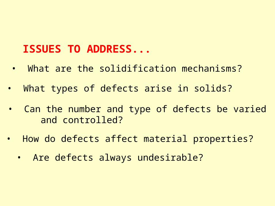
ISSUES TO ADDRESS...
• What types of defects arise in solids?
• Can the number and type of defects be varied and controlled?
• How do defects affect material properties?
• Are defects always undesirable?
• What are the solidification mechanisms?
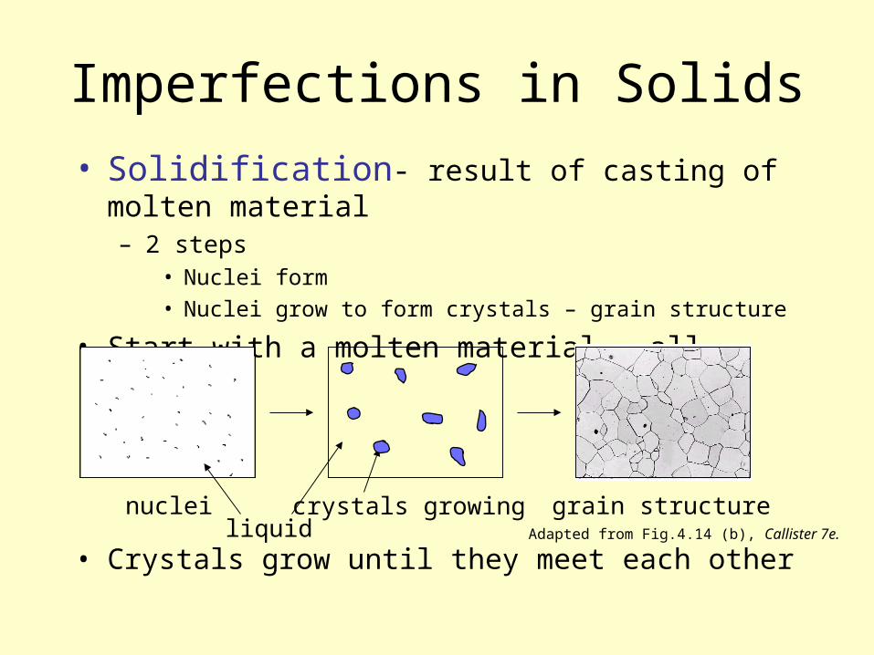
• Solidification- result of casting of molten material– 2 steps
• Nuclei form
• Nuclei grow to form crystals – grain structure
• Start with a molten material – all liquid
Imperfections in Solids
Adapted from Fig.4.14 (b), Callister 7e.
• Crystals grow until they meet each other
nuclei crystals growing grain structureliquid
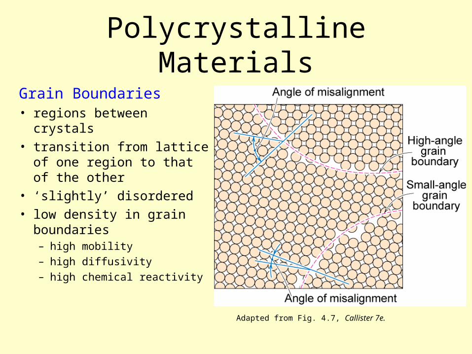
Polycrystalline Materials
Grain Boundaries• regions between crystals• transition from lattice of one
region to that of the other• ‘slightly’ disordered• low density in grain
boundaries– high mobility– high diffusivity– high chemical reactivity
Adapted from Fig. 4.7, Callister 7e.
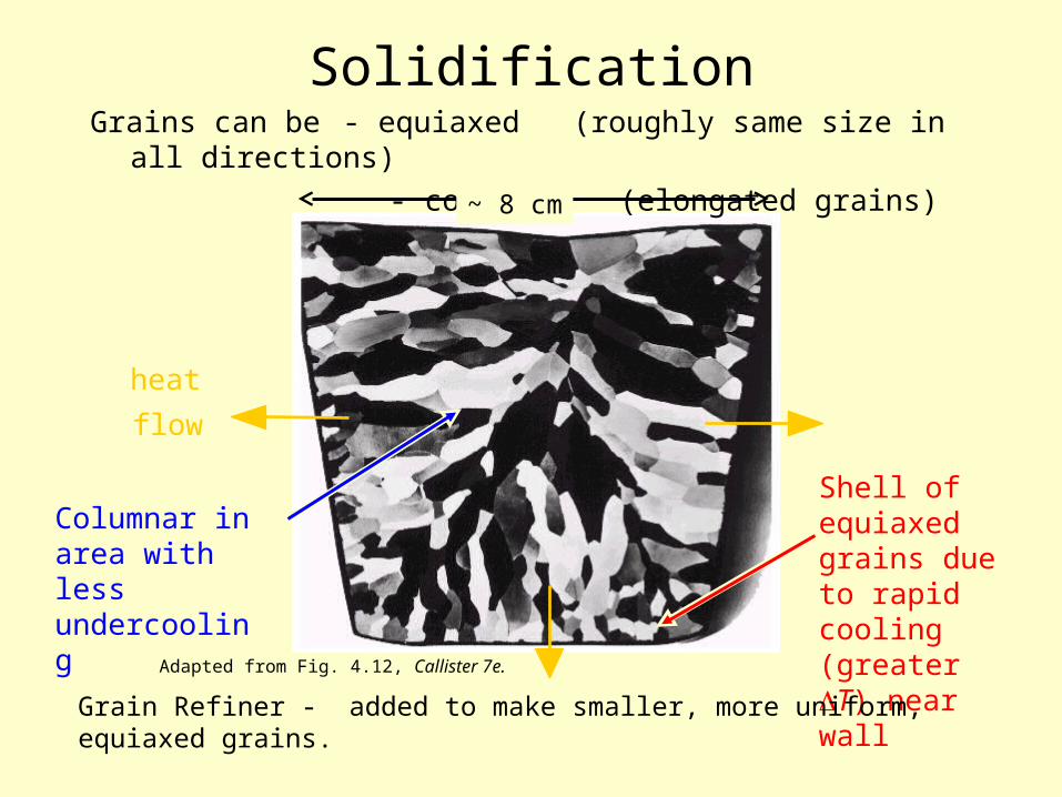
Solidification
Columnar in area with less undercooling
Shell of equiaxed grains due to rapid cooling (greater T) near wall
Grain Refiner - added to make smaller, more uniform, equiaxed grains.
heat
flow
Grains can be - equiaxed (roughly same size in all directions)
- columnar (elongated grains)
Adapted from Fig. 4.12, Callister 7e.
~ 8 cm
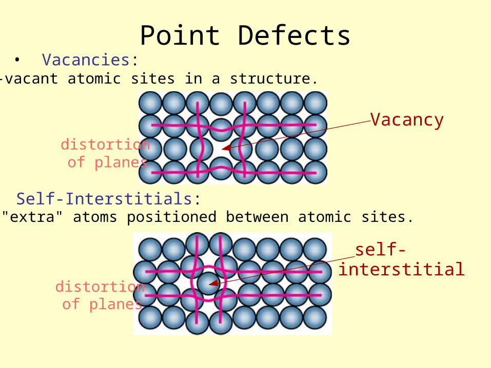
• Vacancies:-vacant atomic sites in a structure.
• Self-Interstitials:-"extra" atoms positioned between atomic sites.
Point Defects
Vacancydistortion of planes
self-interstitial
distortion of planes
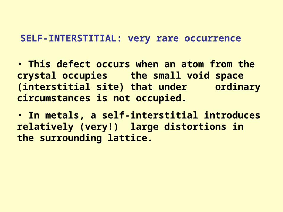
SELF-INTERSTITIAL: very rare occurrence
• This defect occurs when an atom from the crystal occupies the small void space (interstitial site) that under
ordinary circumstances is not occupied.
• In metals, a self-interstitial introduces relatively (very!) large distortions in the surrounding lattice.
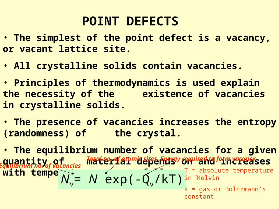
POINT DEFECTS• The simplest of the point defect is a vacancy, or vacant lattice site.
• All crystalline solids contain vacancies.
• Principles of thermodynamics is used explain the necessity of the existence of vacancies in crystalline solids.
• The presence of vacancies increases the entropy (randomness) of the crystal.
• The equilibrium number of vacancies for a given quantity of material depends on and increases with temperature as follows:
Nv= N exp(-Qv/kT)Equilibrium no. of vacancies
Total no. of atomic sites Energy required to form vacancy
T = absolute temperature in Kelvin
k = gas or Boltzmann’s constant
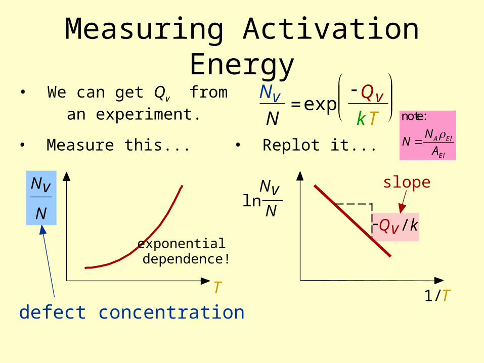
• We can get Qv from an experiment.
Nv
N= exp
Qv
kT
Measuring Activation Energy
• Measure this...
Nv
N
T
exponential dependence!
defect concentration
• Replot it...
1/T
N
Nvln
-Qv /k
slope
note:
A El
El
NN
A
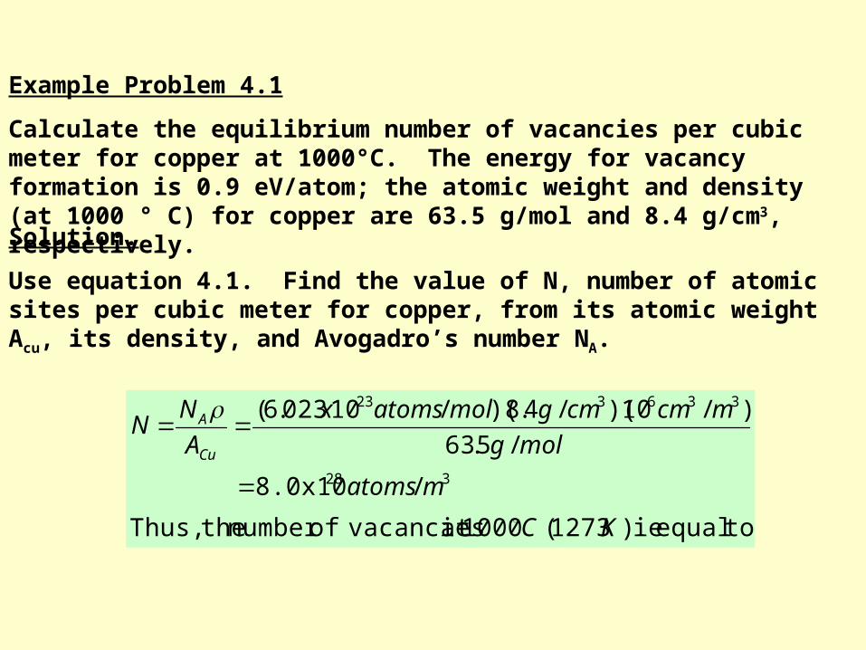
Example Problem 4.1
Calculate the equilibrium number of vacancies per cubic meter for copper at 1000°C. The energy for vacancy formation is 0.9 eV/atom; the atomic weight and density (at 1000 ° C) for copper are 63.5 g/mol and 8.4 g/cm3, respectively.
Solution.
Use equation 4.1. Find the value of N, number of atomic sites per cubic meter for copper, from its atomic weight Acu, its density, and Avogadro’s number NA.
toequal ie )1273( 1000at vacanciesofnumber theThus,
/8.0x10
/5.63
)/10)(/4.8)(/10023.6(
3 28
336323
KC
matoms
molg
mcmcmgmolatomsx
A
NN
Cu
A
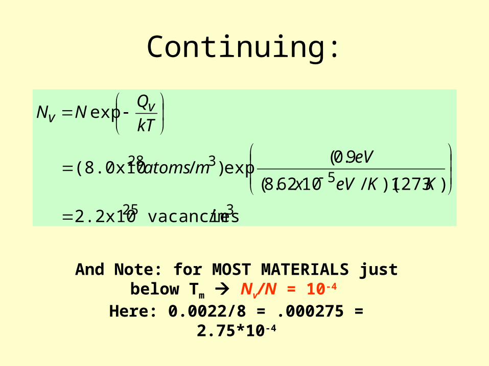
325
5328
/m vacancies2.2x10
)1273)(/1062.8(
9.0(exp)/(8.0x10
exp
KKeVx
eVmatoms
kT
QNN v
v
Continuing:
And Note: for MOST MATERIALS just below Tm Nv/N = 10-4
Here: 0.0022/8 = .000275 = 2.75*10-4
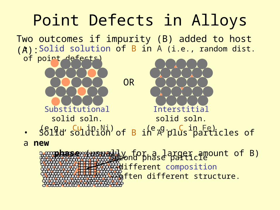
Two outcomes if impurity (B) added to host (A):• Solid solution of B in A (i.e., random dist. of point defects)
• Solid solution of B in A plus particles of a new phase (usually for a larger amount of B)
OR
Substitutional solid soln.(e.g., Cu in Ni)
Interstitial solid soln.(e.g., C in Fe)
Second phase particle--different composition--often different structure.
Point Defects in Alloys
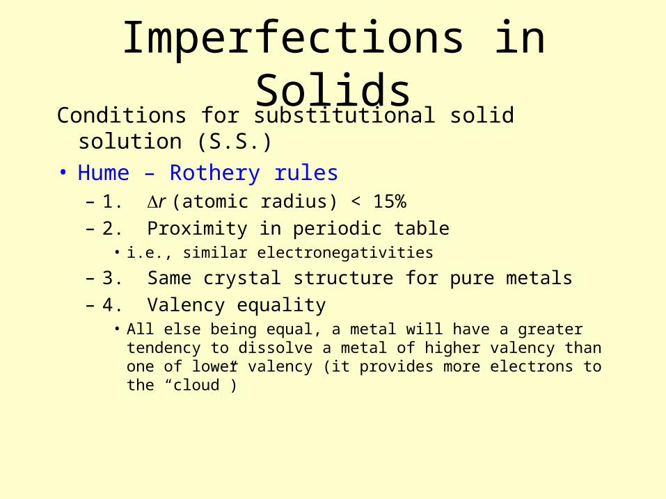
Imperfections in SolidsConditions for substitutional solid solution (S.S.)• Hume – Rothery rules
– 1. r (atomic radius) < 15%– 2. Proximity in periodic table
• i.e., similar electronegativities
– 3. Same crystal structure for pure metals– 4. Valency equality
• All else being equal, a metal will have a greater tendency to dissolve a metal of higher valency than one of lower valency (it provides more electrons to the “cloud”)
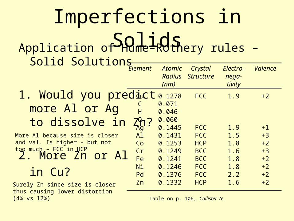
Imperfections in SolidsApplication of Hume–Rothery rules – Solid
Solutions
1. Would you predictmore Al or Ag to dissolve in Zn?
2. More Zn or Al
in Cu?
Table on p. 106, Callister 7e.
Element Atomic Crystal Electro- ValenceRadius Structure nega-
(nm) tivity
Cu 0.1278 FCC 1.9 +2C 0.071H 0.046O 0.060Ag 0.1445 FCC 1.9 +1Al 0.1431 FCC 1.5 +3Co 0.1253 HCP 1.8 +2Cr 0.1249 BCC 1.6 +3Fe 0.1241 BCC 1.8 +2Ni 0.1246 FCC 1.8 +2Pd 0.1376 FCC 2.2 +2Zn 0.1332 HCP 1.6 +2
More Al because size is closer and val. Is higher – but not too much – FCC in HCP
Surely Zn since size is closer thus causing lower distortion (4% vs 12%)
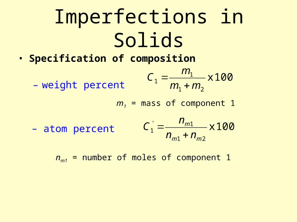
Imperfections in Solids• Specification of composition
– weight percent 100x 21
11 mm
mC
m1 = mass of component 1
100x 21
1'1
mm
m
nn
nC
nm1 = number of moles of component 1
– atom percent
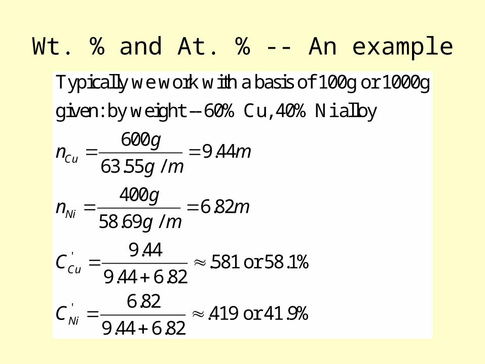
Wt. % and At. % -- An example
'
'
Typically we work with a basis of 100g or 1000g
given: by weight -- 60% Cu, 40% Ni alloy
6009.44
63.55 /
4006.82
58.69 /
9.44.581 or 58.1%
9.44 6.826.82
.419 or 41.9%9.44 6.82
Cu
Ni
Cu
Ni
gn m
g m
gn m
g m
C
C
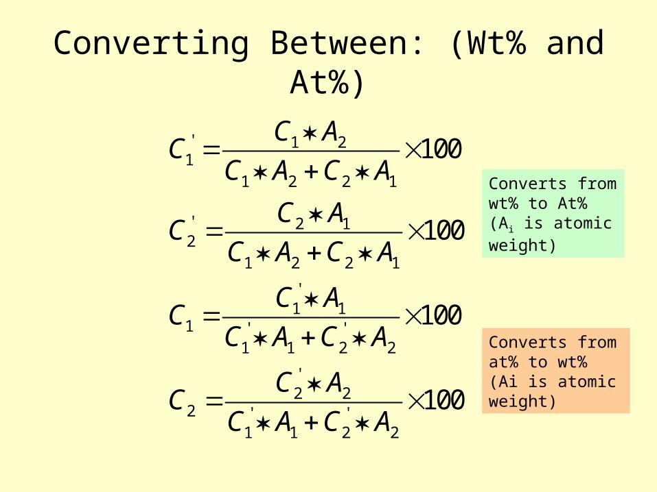
Converting Between: (Wt% and At%)
' 1 21
1 2 2 1
' 2 12
1 2 2 1
'1 1
1 ' '1 1 2 2
'2 2
2 ' '1 1 2 2
100
100
100
100
C AC
C A C A
C AC
C A C A
C AC
C A C A
C AC
C A C A
Converts from wt% to At% (Ai is atomic weight)
Converts from at% to wt% (Ai is atomic weight)
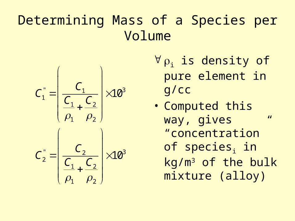
Determining Mass of a Species per Volume
" 311
1 2
1 2
" 322
1 2
1 2
10
10
CC
C C
CC
C C
i is density of pure element in g/cc
• Computed this way, gives “concentration” of speciesi in kg/m3 of the bulk mixture (alloy)
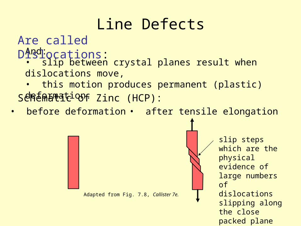
And:• slip between crystal planes result when dislocations move,• this motion produces permanent (plastic) deformation.
Are called Dislocations:
Schematic of Zinc (HCP):• before deformation • after tensile elongation
slip steps which are the physical evidence of large numbers of dislocations slipping along the close packed plane {0001}
Line Defects
Adapted from Fig. 7.8, Callister 7e.
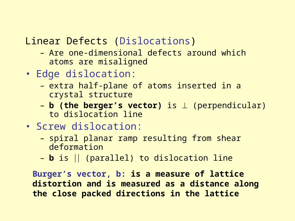
Linear Defects (Dislocations)– Are one-dimensional defects around which atoms are
misaligned
• Edge dislocation:– extra half-plane of atoms inserted in a crystal structure– b (the berger’s vector) is (perpendicular) to dislocation
line
• Screw dislocation:– spiral planar ramp resulting from shear deformation– b is (parallel) to dislocation line
Burger’s vector, b: is a measure of lattice distortion and is measured as a distance along the close packed directions in the lattice
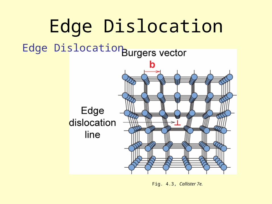
Edge Dislocation
Fig. 4.3, Callister 7e.
Edge Dislocation
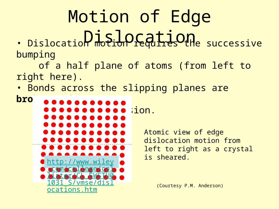
• Dislocation motion requires the successive bumping of a half plane of atoms (from left to right here).• Bonds across the slipping planes are broken and remade in succession.
Atomic view of edgedislocation motion fromleft to right as a crystalis sheared.
(Courtesy P.M. Anderson)
Motion of Edge Dislocation
http://www.wiley.com/college/callister/CL_EWSTU01031_S/vmse/dislocations.htm
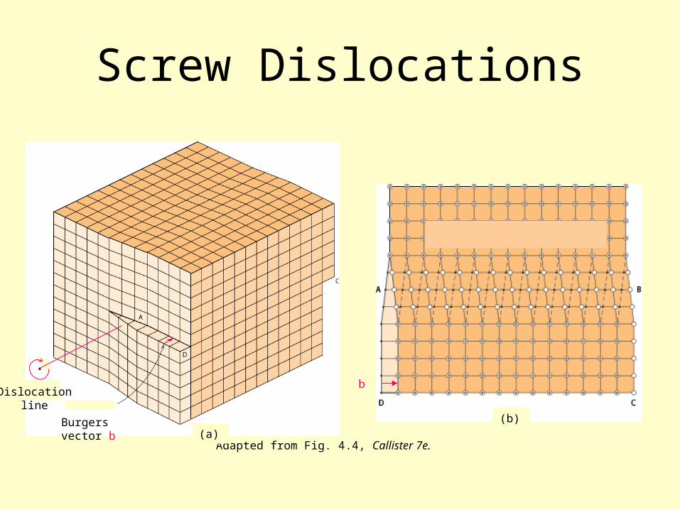
Screw Dislocations
Adapted from Fig. 4.4, Callister 7e.
Burgers vector b
Dislocationline
b
(a)(b)
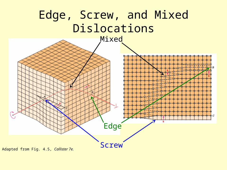
Edge, Screw, and Mixed Dislocations
Adapted from Fig. 4.5, Callister 7e.
Edge
Screw
Mixed
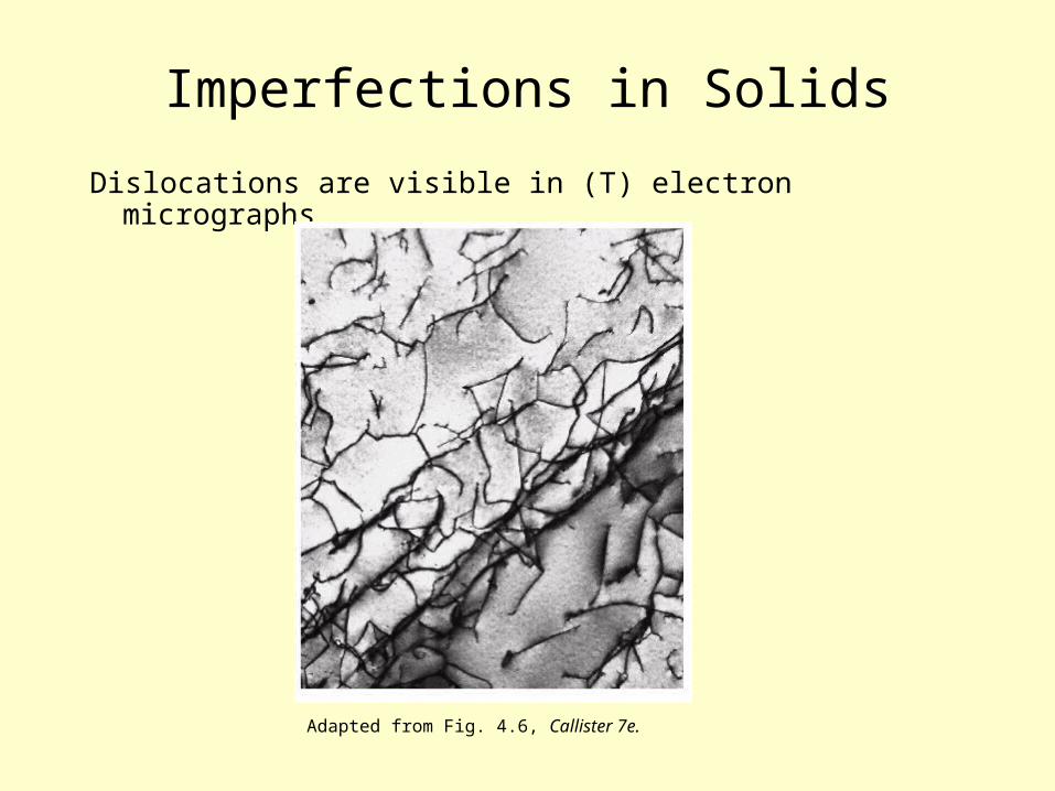
Imperfections in Solids
Dislocations are visible in (T) electron micrographs
Adapted from Fig. 4.6, Callister 7e.
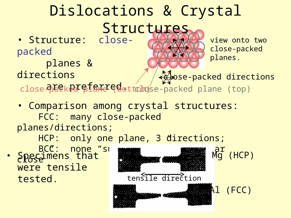
Dislocations & Crystal Structures• Structure: close-packed planes & directions are preferred.
view onto twoclose-packedplanes.
close-packed plane (bottom) close-packed plane (top)
close-packed directions
• Comparison among crystal structures: FCC: many close-packed planes/directions; HCP: only one plane, 3 directions; BCC: none “super-close” many “near close”
• Specimens that were tensile tested.
Mg (HCP)
Al (FCC)tensile direction
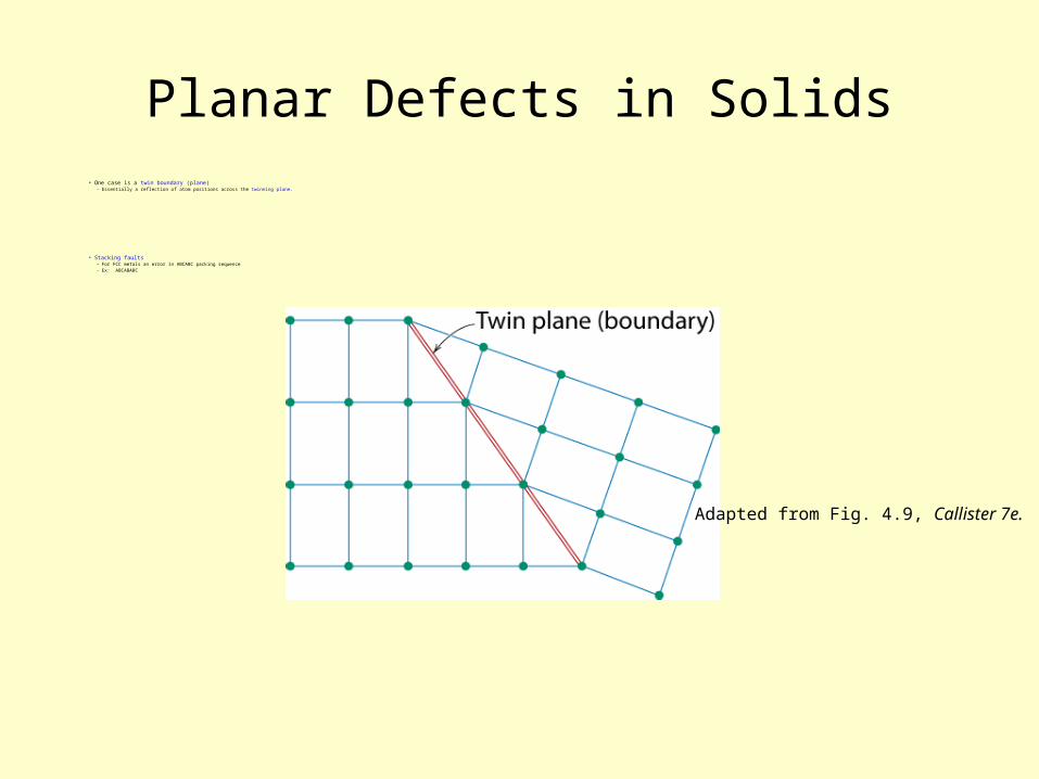
Planar Defects in Solids• One case is a twin boundary (plane)
– Essentially a reflection of atom positions across the twinning plane.
• Stacking faults– For FCC metals an error in ABCABC packing sequence– Ex: ABCABABC
Adapted from Fig. 4.9, Callister 7e.
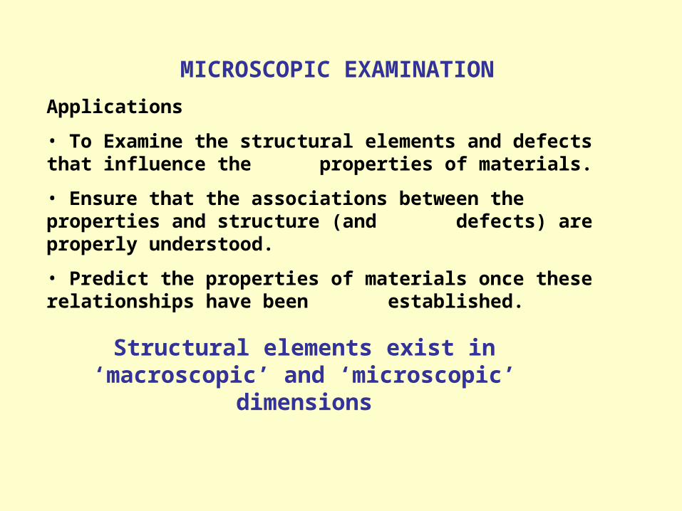
MICROSCOPIC EXAMINATION
Applications
• To Examine the structural elements and defects that influence the properties of materials.
• Ensure that the associations between the properties and structure (and defects) are properly understood.
• Predict the properties of materials once these relationships have been established.
Structural elements exist in ‘macroscopic’ and ‘microscopic’ dimensions
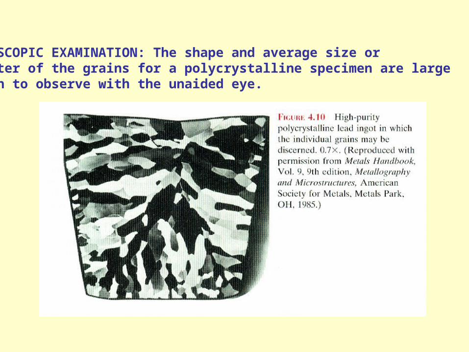
MACROSCOPIC EXAMINATION: The shape and average size ordiameter of the grains for a polycrystalline specimen are large enough to observe with the unaided eye.
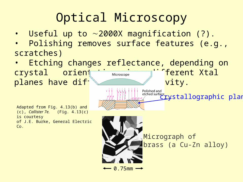
• Useful up to 2000X magnification (?).• Polishing removes surface features (e.g., scratches)• Etching changes reflectance, depending on crystal orientation since different Xtal planes have different reactivity.
Micrograph ofbrass (a Cu-Zn alloy)
0.75mm
Optical Microscopy
Adapted from Fig. 4.13(b) and (c), Callister 7e. (Fig. 4.13(c) is courtesyof J.E. Burke, General Electric Co.
crystallographic planes
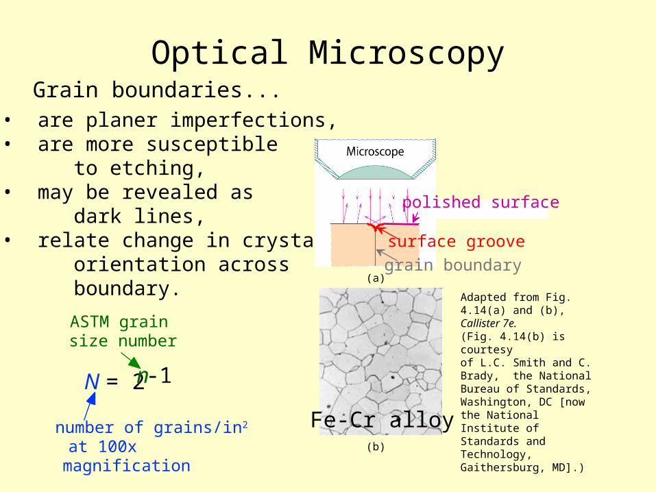
Grain boundaries...• are planer imperfections,• are more susceptible to etching,• may be revealed as dark lines,• relate change in crystal orientation across boundary. Adapted from Fig. 4.14(a)
and (b), Callister 7e.(Fig. 4.14(b) is courtesyof L.C. Smith and C. Brady, the National Bureau of Standards, Washington, DC [now the National Institute of Standards and Technology, Gaithersburg, MD].)
Optical Microscopy
ASTM grain size number
N = 2n-1
number of grains/in2 at 100x magnification
Fe-Cr alloy(b)
grain boundary
surface groove
polished surface
(a)
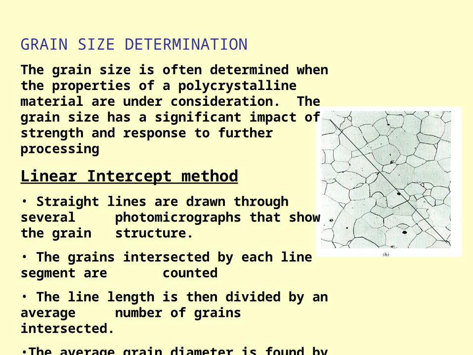
GRAIN SIZE DETERMINATION
The grain size is often determined when the properties of a polycrystalline material are under consideration. The grain size has a significant impact of strength and response to further processing
Linear Intercept method
• Straight lines are drawn through several photomicrographs that show the grain structure.
• The grains intersected by each line segment are counted
• The line length is then divided by an average number of grains intersected.
•The average grain diameter is found by dividing this result by the linear magnification of the
photomicrographs.
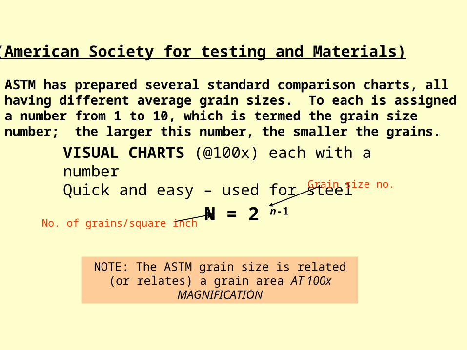
ASTM (American Society for testing and Materials)
VISUAL CHARTS (@100x) each with a number Quick and easy – used for steel
ASTM has prepared several standard comparison charts, all having different average grain sizes. To each is assigned a number from 1 to 10, which is termed the grain size number; the larger this number, the smaller the grains.
N = 2 n-1No. of grains/square inch
Grain size no.
NOTE: The ASTM grain size is related (or relates) a grain area AT 100x MAGNIFICATION
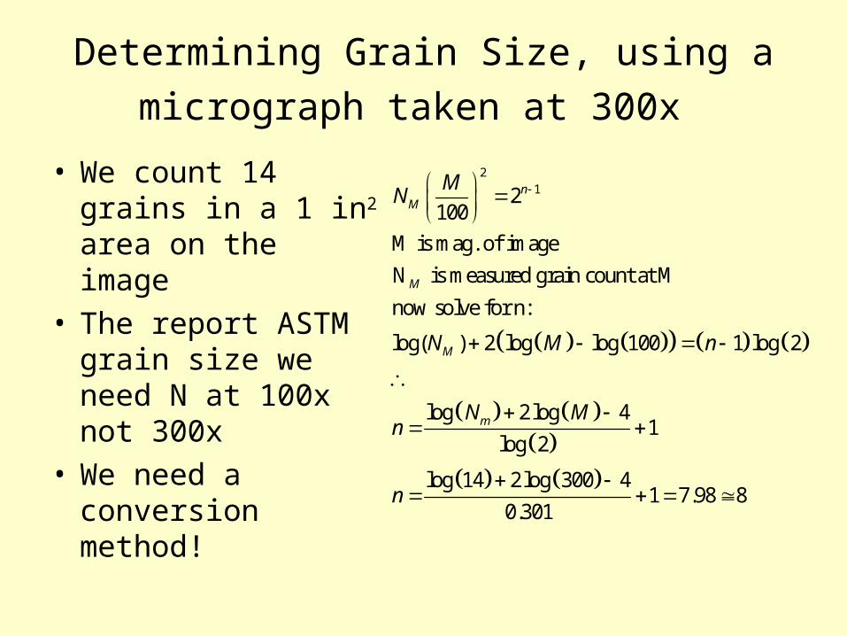
Determining Grain Size, using a micrograph
taken at 300x • We count 14 grains
in a 1 in2 area on the image
• The report ASTM grain size we need N at 100x not 300x
• We need a conversion method!
212
100
M is mag. of image
N is measured grain count at M
now solve for n:
log( ) 2 log log 100 1 log 2
log 2log 41
log 2
log 14 2log 300 41 7.98 8
0.301
nM
M
M
m
MN
N M n
N Mn
n
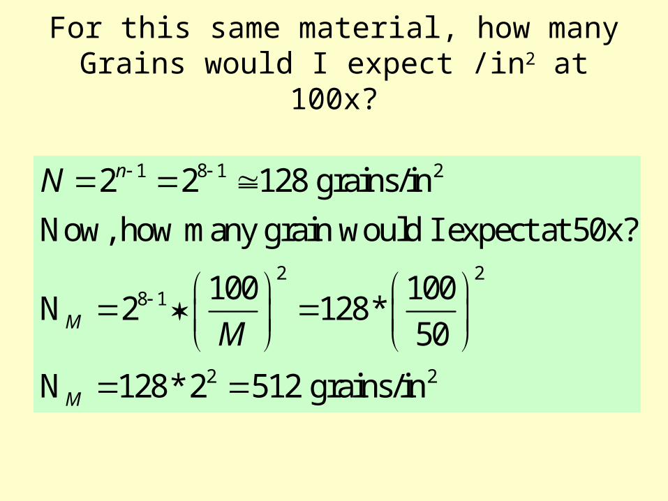
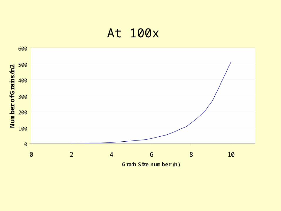
For this same material, how many Grains would I expect /in2 at 100x?
1 8 1 2
2 28 1
2 2
2 2 128 grains/in
Now, how many grain would I expect at 50x?
100 100N 2 128*
50
N 128*2 512 grains/in
n
M
M
N
M
0
100
200
300
400
500
600
0 2 4 6 8 10 12
Grain Size number (n)
Nu
mb
er o
f G
rain
s/in
2
At 100x
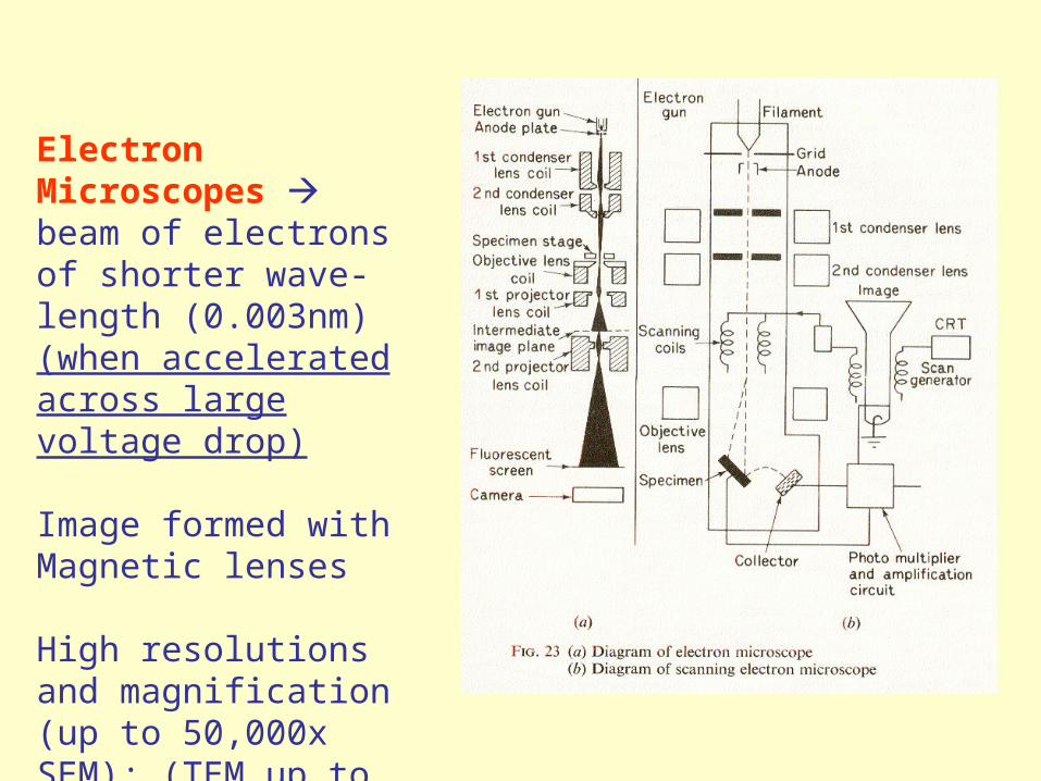
Electron Microscopes beam of electrons of shorter wave-length (0.003nm) (when accelerated across large voltage drop)
Image formed with Magnetic lenses
High resolutions and magnification (up to 50,000x SEM); (TEM up to 1,000,000x)
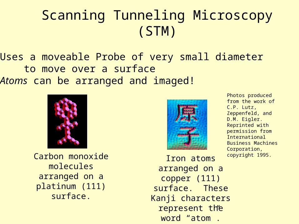
• Uses a moveable Probe of very small diameter to move over a surface
• Atoms can be arranged and imaged!
Carbon monoxide molecules arranged on a platinum (111)
surface.
Photos produced from the work of C.P. Lutz, Zeppenfeld, and D.M. Eigler. Reprinted with permission from International Business Machines Corporation, copyright 1995.
Iron atoms arranged on a copper (111)
surface. These Kanji characters represent
the word “atom”.
Scanning Tunneling Microscopy (STM)
Summary
• Point, Line, and Area defects exist in solids.• The number and type of defects can be varied and
controlled – T controls vacancy conc.– amount of plastic deformation controls # of dislocations– Weight of charge materials determine concentration of
substitutional or interstitial point ‘defects’
• Defects affect material properties (e.g., grain boundaries control crystal slip).
• Defects may be desirable or undesirable – e.g., dislocations may be good or bad, depending on whether
plastic deformation is desirable or not.– Inclusions can be intention for alloy development