Embed Size (px)
Citation preview

Imaging Science Fundamentals Chester F. Carlson Center for Imaging Science
Digital Imaging: CCDsDigital Imaging: CCDs
Imaging Science Fundamentals

Imaging Science Fundamentals Chester F. Carlson Center for Imaging Science
Charge Coupled Charge Coupled Device (CCD)Device (CCD)
CCD replaces AgX film
Based on silicon chip
Disadvantages vs. AgX: Difficulty/cost of CCD
manufacture; large arrays are
VERY expensive
“Young” technology; rapidly
changing
Light Sensitive Area

Imaging Science Fundamentals Chester F. Carlson Center for Imaging Science
Response of CCDResponse of CCD
The response of CCD is linear (i.e., if 10,000 captured photons corresponds to a digital count of 4, then 20,000 photons captured yields a digital count of 8)
Linearity is critical for scientific uses of CCD
Log H
Den
sity
Response of photographicnegative
Exposure
Dig
ital
Cou
nt
Response of CCD
Imaging Science Fundamentals Chester F. Carlson Center for Imaging Science
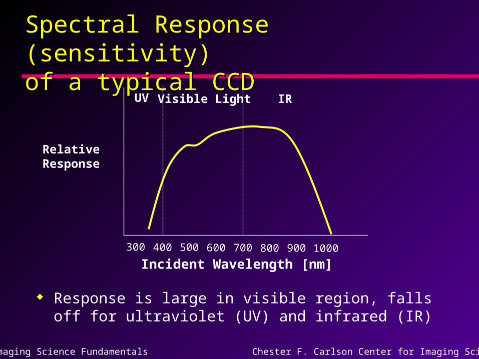
Spectral Response (sensitivity) Spectral Response (sensitivity) of a typical CCDof a typical CCD
Response is large in visible region, falls off for ultraviolet (UV) and infrared (IR)
300 400 500 600 700 800 900 1000
Incident Wavelength [nm]
RelativeResponse
Visible Light IRUV
Imaging Science Fundamentals Chester F. Carlson Center for Imaging Science
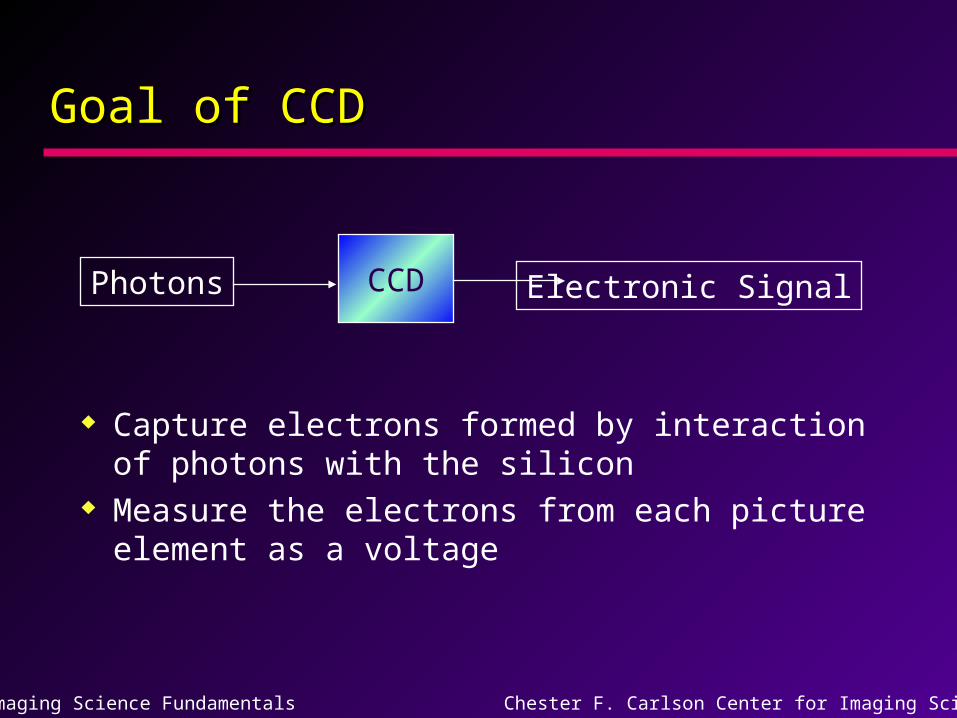
Goal of CCDGoal of CCD
Capture electrons formed by interaction of photons with the silicon
Measure the electrons from each picture element as a voltage
CCDPhotons Electronic Signal
Imaging Science Fundamentals Chester F. Carlson Center for Imaging Science
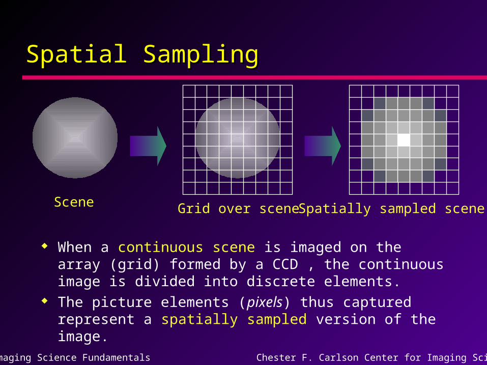
Spatial SamplingSpatial Sampling
When a continuous scene is imaged on the array (grid) formed by a CCD , the continuous image is divided into discrete elements.
The picture elements (pixels) thus captured represent a spatially sampled version of the image.
Scene Grid over scene Spatially sampled scene

Imaging Science Fundamentals Chester F. Carlson Center for Imaging Science
Basic structure of CCDBasic structure of CCD
Divided into small elements called pixels (picture elements).
preamplifier
Image Image Capture Capture AreaArea
Shift Register
Voltageout
Columns
Rows
Imaging Science Fundamentals Chester F. Carlson Center for Imaging Science
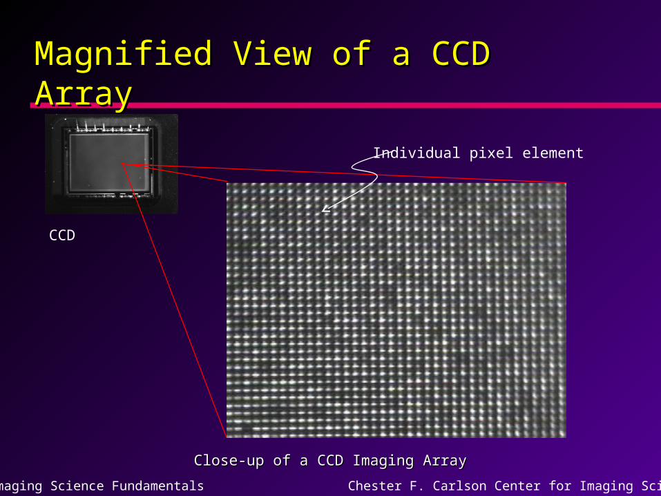
Magnified View of a CCD ArrayMagnified View of a CCD Array
Individual pixel element
Close-up of a CCD Imaging ArrayClose-up of a CCD Imaging Array
CCD

Imaging Science Fundamentals Chester F. Carlson Center for Imaging Science
CCDs as SemiconductorsCCDs as Semiconductors
Conductors allow electricity to pass through. (Metals like copper and gold are conductors.)
Insulators do not allow electricity to pass through. (Plastic, wood, and paper are insulators.)
Some materials are halfway in between, and are called semiconductors.
ConductorInsulator
Imaging Science Fundamentals Chester F. Carlson Center for Imaging Science
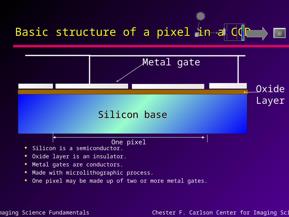
Basic structure of a pixel in a CCDBasic structure of a pixel in a CCD
Silicon is a semiconductor. Oxide layer is an insulator. Metal gates are conductors. Made with microlithographic process. One pixel may be made up of two or more metal gates.
Silicon baseSilicon base
Metal gate
Oxide Layer
One pixel

Imaging Science Fundamentals Chester F. Carlson Center for Imaging Science
Photon/Silicon InteractionPhoton/Silicon Interaction
Photon knocks off one of the electrons from the silicon matrix.
Silicone-e-
Electron “wanders around” randomly through the matrix. Electron gets absorbed into the silicon matrix after some period.

Imaging Science Fundamentals Chester F. Carlson Center for Imaging Science
Collection stageCollection stage
Voltage applied to the metal gates produces a depletion region in the silicon. (depleted of electrons)
Depletion region is the “light sensitive” area where electrons formed from the photon interacting with the silicon base are collected.
Voltage

Imaging Science Fundamentals Chester F. Carlson Center for Imaging Science
Collection stageCollection stage
Electron formed in the silicon matrix by a photon.
e-
Electron wanders around the matrix.
If the electron wanders into the depletion region, the electron is captured, never recombining with the silicon matrix.
e-e-
Voltage

Imaging Science Fundamentals Chester F. Carlson Center for Imaging Science
CollectionCollection
The number of electrons accumulated is proportional to the amount of light that hit the pixel.
There is a maximum number of electron that these “wells” can hold.
e-
e-e- e-e- e-e-e- e-
e- e-
Light

Imaging Science Fundamentals Chester F. Carlson Center for Imaging Science
ReadoutReadout
How do you access so much data efficiently? (i.e. a 1024 x 1024 CCD has 1,048,576 pixels!) Possible solutions:
1. Have output for individual pixels. Too many “wires”
2. Somehow move the charges across the CCD array and read out one by one.
Bucket Brigade

Imaging Science Fundamentals Chester F. Carlson Center for Imaging Science
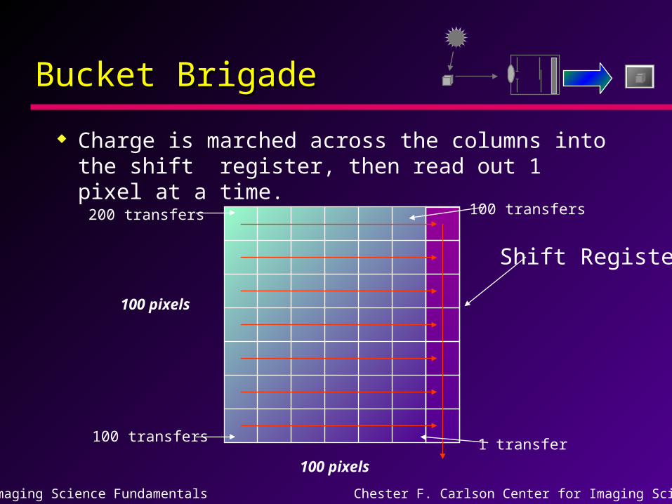
Bucket BrigadeBucket Brigade
By alternating the voltage applied to the metal gates, collected electrons may be moved across the columns.
e-
e-e- e-e- e-e-e- e-
e- e-e-
e-e- e-e- e-e- e-
e- e- e-e-e-e- e-
e- e- e-e- e-e- e-e- e-e-e-
e- e- e-e- e-e- e-e- e- e-e-e-
e-e-e- e-e- e-e- e- e-
e-e-e-e-e-
e-e- e-
Imaging Science Fundamentals Chester F. Carlson Center for Imaging Science
Bucket BrigadeBucket Brigade
Charge is marched across the columns into the shift register, then read out 1 pixel at a time.
100 pixels
100 pixels
1 transfer100 transfers
100 transfers200 transfers
Shift Register
Imaging Science Fundamentals Chester F. Carlson Center for Imaging Science
Converting Analog Voltages to DigitalConverting Analog Voltages to Digital
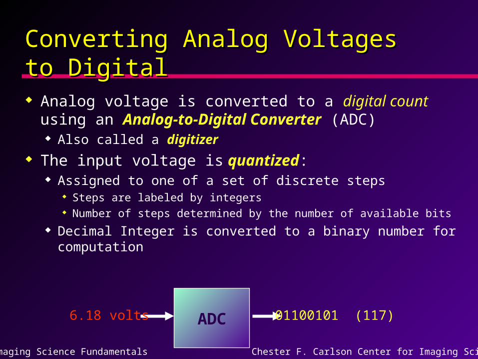
Analog voltage is converted to a digital count using an Analog-to-Digital Converter (ADC) Also called a digitizer
The input voltage is quantized: Assigned to one of a set of discrete steps
Steps are labeled by integers Number of steps determined by the number of available bits
Decimal Integer is converted to a binary number for computation
ADC6.18 volts 01100101 (117)

Imaging Science Fundamentals Chester F. Carlson Center for Imaging Science
Bits and BytesBits and Bytes
In the digital domain, there are only two possible numbers in a digit: 0 or 1.
This numbering system is called a binary system. Each digit is called a bit (Binary digIT). Byte is 8 bits
Decimal012345
Binary011011100101
Imaging Science Fundamentals Chester F. Carlson Center for Imaging Science
BitsBits
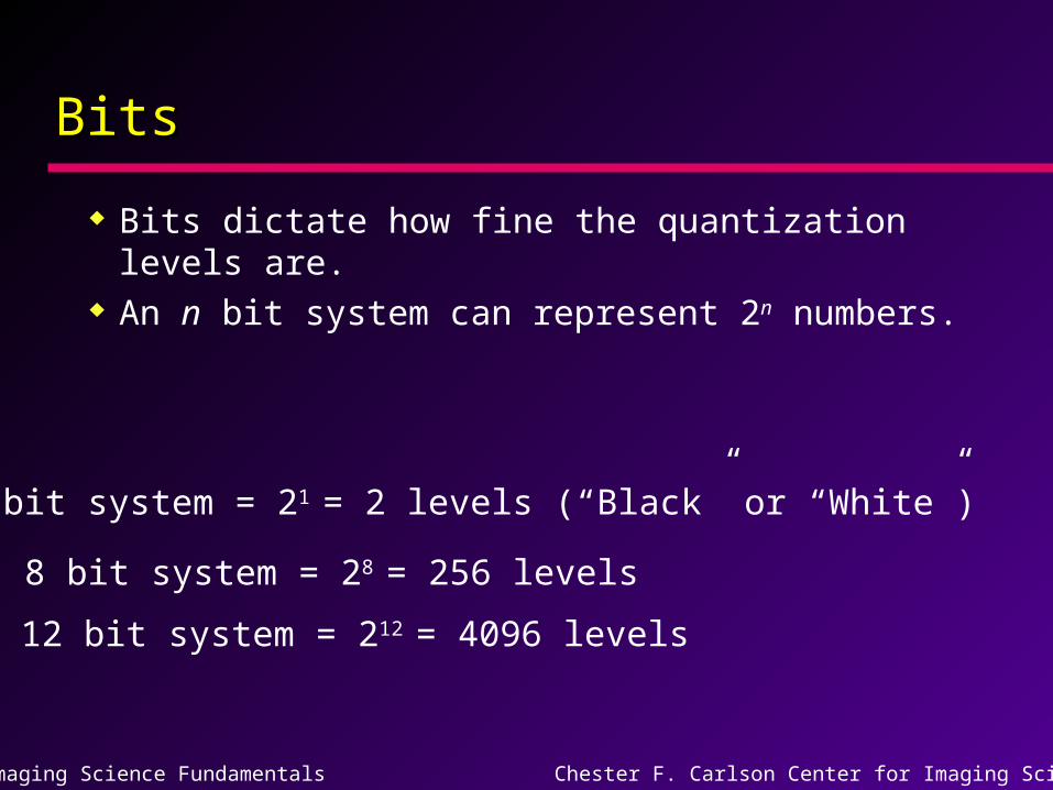
Bits dictate how fine the quantization levels are.
An n bit system can represent 2n numbers.
1 bit system = 21 = 2 levels (“Black” or “White”)
8 bit system = 28 = 256 levels
12 bit system = 212 = 4096 levels

Imaging Science Fundamentals Chester F. Carlson Center for Imaging Science
QuantizationQuantization
Let’s say our 8 bit ADC accepts input voltage range of 0 to 10v.
ADC
6.8 volts
Since there are 256 discrete levels in an 8 bit system, each level will be 10v/256 or 0.0390625 volts per analog-to-digital unit (ADU).
So, if the input voltage was 6.8 volts . . .
6.8v 174.08
Volts DC
Since ADU are stored as binary integers, the decimal must be truncated (to 174).
172
173
174
175
176
255
00v
6.8 volts/0.0390625 volts per DC = 174.08
10v
Binary equivalent of 174 is 10101110.

Imaging Science Fundamentals Chester F. Carlson Center for Imaging Science
QuantizationQuantization
Spatially sampled image can now be turned into numbers according to the brightness of each pixel.
Spatially sampled scene
0
0
0
0
0
0
0
0
0
0
0
0
0
0
25
40
0
0
25
40
40
25 25
2540 40
40 40 40
25 2540 40 40
40 40 25
40
40
40
64
64
64
64
64
64
64 64 64
64 64 64
97
97
97
97
97
150
97
97
97
0 0 0 0 0 0
0 0 0 0 0 0
0
0
0
0
0 0
0
0
Numerical representation