Embed Size (px)
Citation preview

This article has been accepted for inclusion in a future issue of this journal. Content is final as presented, with the exception of pagination.
IEEE TRANSACTIONS ON MICROWAVE THEORY AND TECHNIQUES 1
Miniaturized UWB Filters Integrated With TunableNotch Filters Using a Silicon-Based Integrated
Passive Device TechnologyZhengzheng Wu, Student Member, IEEE, Yonghyun Shim, Student Member, IEEE, and
Mina Rais-Zadeh, Member, IEEE
Abstract—This paper reports on the implementation of minia-turized ultra-wideband filters integrated with tunable notch fil-ters using a silicon-based integrated passive device technology. Anultra-wideband bandpass filter is realized on a micromachined sil-icon substrate, showing an insertion loss of 1.1 dB, return loss ofbetter than 15 dB, and attenuation of more than 30 dB at bothlower and upper stop-bands, with a spurious-free response up to40 GHz. The filter occupies only 2.9 mm 2.4 mm of die area.To address the in-band interference issues associated with ultra-wideband communication, very compact tunable notch filters aremonolithically integrated with the bandpass filters. A two-pole tun-able notch filter integrated with an ultra-wideband filter providesmore than 20 dB rejection in the 5–6 GHz range to reject U-NII in-terferences, with a total footprint of 4.8 mm 2.9 mm. The powerhandling, linearity, and temperature stability of filters are charac-terized and presented in this paper.
Index Terms—Integrative passive devices (IPDs) and modules,interference suppression, MEMS or microelectromechanical sys-tems, tunable filters, ultra-wideband.
I. INTRODUCTION
U LTRA-WIDEBAND (UWB) has emerged as a fastgrowing technology since the Federal Communications
Commission (FCC) approved the unlicensed use of the fre-quency spectrum from 3.1 to 10.6 GHz [1]. The allocated widespectrum enables Impulse Radio-UWB (IR-UWB), which isbased on transmitting and detecting short duration pulses. Incontrast to narrowband systems, IR-UWB is carrier-less, greatlysimplifying the RF front-end by using all-digital transmitters[2], [3] and receivers that do not require power hungry RFoscillators or PLLs [4], [5]. The low-cost and energy-efficientIR-UWB scheme is a good candidate for several applications,such as wireless sensor networks and handheld devices.UWB communication stimulates both opportunities and chal-
lenges in the design and implementation of fully integrated RFfront-ends [2]–[6]. Still, a major impediment to the wide adop-tion of UWB technology is the issue of narrowband interfer-ences that might exist in the same frequency range. The FCC-
Manuscript received September 26, 2011; revised November 07, 2011; ac-cepted November 18, 2011. This work was supported in part by the NationalScience Foundation under Award 1055308 and in part by the University ofMichigan, Ann Arbor.The authors are with the University of Michigan, Ann Arbor, MI 48109 USA
(e-mail: [email protected]; [email protected]).Color versions of one or more of the figures in this paper are available online
at http://ieeexplore.ieee.org.Digital Object Identifier 10.1109/TMTT.2011.2178428
regulated low UWB emission power ( 41.3 dBm/MHz) neces-sitates interference mitigation techniques. Circuit design tech-niques, such as frequency selective receivers, have been ex-plored to reject the interferences using active filters, but at thecost of increased CMOS chip area and higher power consump-tion [7], [8]. Alternatively, RF front-ends exploiting only sub-bands of the UWB frequency range have been used to addressthe interference issue [9], [10], although with reduced commu-nication capacity. It is known that RF preselect filtering greatlyrelaxes the receiver linearity requirement and reduces the gaindesensitization due to strong interferers. Also, for IR-UWB, fil-ters used in transmitters can regulate the emission power ofshort duration pulses to comply with the FCC spectral maskand eliminate the use of additional pulse shaping circuits as in[11]. Therefore, low-loss, highly selective, and integrated pas-sive UWB filters are needed.So far, reported works have focused on UWB filter minia-
turization based on microstrip, coplanar waveguide (CPW), orquasi-lumped components on low-loss microwave substratessuch as FR4, LTCC, or LCP [12]–[19]. These filter imple-mentations are developed mostly as standalone components.Our recent work demonstrated, for the first time, low-loss andminiaturized UWB filters fully integrated with fixed notchfilters on silicon substrates using an integrated passive devices(IPD) technology [20]. In this paper, the proposed IPD tech-nology is employed to fabricate UWB filters integrated with RFmicroelectromechanical system (MEMS) tunable notch filters.The tunable notch filters in this work are some of the mostcompact filters reported [21]–[28] that provide interferencerejection of more than 20 dB (in 4.9–6.5 GHz frequency range)and low passband loss. Integration of UWB filters with tunablenotches allows detect-and-avoid (DAA) mechanism, whichcan address the issue of interferences. Using the multibandorthogonal frequency division multiplexing (MB-OFDM), theDAA-enabled UWB radio can form the basis for cognitiveradio implementation [29].In this paper, first the IPD technology will be introduced.
Then, the UWB and tunable notch filter design techniques thatachieve size miniaturization and high-performance filtering willbe discussed. Finally, integration result of the UWB filter withthe tunable notch filter will be presented and characterizationresults of filters will be discussed. The presented filter tech-nology is suitable for flip-chip assembly or multi-chip-module(MCM) integration with CMOS ICs, making the implementa-tion of highly integrated UWBRF front-end modules realizable.
0018-9480/$31.00 © 2012 IEEE

This article has been accepted for inclusion in a future issue of this journal. Content is final as presented, with the exception of pagination.
2 IEEE TRANSACTIONS ON MICROWAVE THEORY AND TECHNIQUES
Fig. 1. Conceptual view of the IPDmulti-chip integration (top) and the processflow of the IPD technology (bottom).
II. FABRICATION PROCESS FLOW OF THE INTEGRATED PASSIVEDEVICE (IPD) TECHNOLOGY PLATFORM
The UWB filters are fabricated using a silicon-based IPDtechnology, schematically shown in Fig. 1 (top). Using thisprocess, RF MEMS tunable capacitors, switches, and high-inductors can be simultaneously fabricated. When wafer-levelpackaged, the all-in-one IPD is expected to offer a more com-pact form factor and a lower cost passive integration schemecompared to other RF MEMS technologies.The fabrication process is shown in Fig. 1. The process starts
with the deposition of a 2 -thick low-stress silicon oxyni-tride (SiON) dielectric layer on a high-resistivitysilicon substrate. The processing steps are: (a) deposition andpatterning of gold as the bottom electrode; (b) deposition ofa dielectric layer for metal-insulator-metal (MIM) capacitors;(c) deposition and patterning of an amorphous silicon sacrificiallayer; (d) etching the sacrificial layer to form a step for realizinghigh tuning ratio MEMS tunable capacitors and ohmic-contactdimples; (e) gold electroplating for the top metal electrode ofMIM capacitors; (e) thick copper electroplating to form high-inductive components; and (f) xenon difluoride gaseous etchingof the amorphous silicon to form air-gap membrane, and selec-tively removing the silicon substrate to reduce the substrate loss.Where the silicon substrate is partially removed, the SiON di-electric membrane provides support for metal structures for en-hanced mechanical robustness. The sacrificial layer step etchallows the formation of dual gaps for high analog tuning range( 4:1) MEMS capacitors [30], [31], and contact dimples usedin ohmic-contact MEMS switches [32].
III. DESIGN AND IMPLEMENTATION OF FILTERS
Using the presented IPD platform, UWB bandpass filters aswell as tunable planar notch filters are demonstrated. Filtersare designed in co-planar configuration with proximate groundplane so that the electromagnetic field is confined on the sur-face of the substrate. Therefore, the performance of filters is not
Fig. 2. A SEM image of a cascaded bandpass filter on a micromachined sub-strate (size: 2.9 mm 2.4 mm). Inset shows the inductor on a SiON membrane.
Fig. 3. (a) High-pass filter circuit, and (b) layout of coupled inductors.
affected by backside metallization, variations in the substratethickness, or the packaging layer.To accurately predict parasitic effects of the co-planar filter
configuration, filters are simulated using the HFSS full-waveelectromagnetic simulation tool [33]. In all HFSS simula-tions, the conductivity of electroplated copper is taken as
and the loss tangent and conductivity of thesilicon substrate are assumed to be 0.004, and 1 , re-spectively. In the following subsections, the design strategy ofthe UWB filters, tunable notch filters, and UWB filter with anintegrated tunable notch will be discussed, and the simulationresults of the filters will be compared with measured results.
A. Cascaded UWB Bandpass Filter
Previously we reported on a UWB bandpass filter designcomposed of a cascade of low-pass and high-pass filter sectionsthat offers low loss on both micromachined and solid siliconsubstrates (Fig. 2) [20]. The filter networks were synthesizedfrom generalized Chebyshev configuration [34], providingsteep rejection with a low-order design. Fig. 3(a) shows thecircuit diagram of the high-pass filter section. From the filtersynthesis and optimization, the value of the components forthe high-pass filter having a cutoff frequency of 3.1 GHz andout-of-band rejection of 30 dB below 2 GHz can be obtained.The derived filter network contains a high-value inductor, ,in the T-junction, which can be eliminated by transformingthe T-junction into a pair of mutually coupled inductors [35].The component values of the coupled inductor pair are listedin Table I.Mutual coupling of 0.2 is difficult to implement using ei-
ther tightly coupled interleaved structures [36] or loosely cou-pled proximate inductor pairs. Therefore, a custom-designedinter-winded inductor pair is used [Fig. 3(b)]. The inter-windedpair has tight coupling in the inner turns and weak coupling in

This article has been accepted for inclusion in a future issue of this journal. Content is final as presented, with the exception of pagination.
WU et al.: MINIATURIZED UWB FILTERS INTEGRATED WITH TUNABLE NOTCH FILTERS 3
Fig. 4. (a) Low-pass filter circuit and (b) layout of the coupled inductor pair.
TABLE ICOMPONENTS IN THE HIGH-PASS FILTER
TABLE IICOMPONENTS IN THE LOW-PASS FILTER
Fig. 5. Measured response of the cascaded high-pass–low-pass bandpass filteron a micromachined substrate (silicon is removed beneath inductors). (a) Inser-tion loss and return loss (with closed-up view of passband performance inset).(b) Group delay.
the outer turns of the inductors, offering the desired mutual cou-pling of 0.2. The relatively small size of these mutually coupledinductors is the main contributing factor in significant size re-duction of the high-pass filter.The circuit diagram of the low-pass filter section of the UWB
filter is shown in Fig. 4(a). Inductors and are purpose-fully coupled by placing them in close proximity, as depicted inFig. 4(b). As a result, the transmission zero is moved close tothe passband to improve the roll-off at the edge of the high-fre-quency cutoff. The component values used in the low-pass filterare listed in Table II. It can be seen that the substrate parasiticcapacitances in the filter can be absorbed into filter components, , and , making it possible to achieve a low-loss filter at
frequencies up to 10 GHz [20]. Fig. 5 shows the measured andsimulated responses of a cascaded (high-pass–low-pass) UWBbandpass filter on a micromachined silicon substrate. The cas-caded UWB filter has a bandwidth of 7.6 GHz (3–10.6 GHz)within which the return loss is better than 15 dB. The mid-bandinsertion loss of the filter is 1.1 dB (at 6.85 GHz). This filterexhibits an excellent out-of-band rejection of at least 30 dB at
Fig. 6. Circuit implementation of the notch filter.
lower ( 2 GHz) and upper ( 13 GHz) sides of the passband.A spurious-free response up to 40 GHz is obtained. The groupdelay is less than 0.25 ns.
B. Tunable Notch Filter
UWB communication using bandpass filters in the receivermay suffer from strong in-band interferers. The center frequen-cies of in-band interferences may not be known in advance.Considering the IEEE 802.11a interferers, for example, narrow-band interferers can appear in a range of 4.9–5.85 GHz. There-fore, a fixed notch filter cannot completely resolve the inter-ference problem of UWB filters. It is also necessary that notchfilters have sufficient rejection level across the communicationband of interferers. As such, analog tuning of a notch filter withhigh rejection level is required to block unknown interferers.Reported works have been focused on the design of fixed-fre-quency narrowband notch filters embedded with UWB band-pass filters [12], [16]–[18], [20]. In this paper, we demonstratetunable notch filters that can be monolithically integrated withUWB filters to mitigate the interference issue.The design of miniaturized notch filters in this work is based
on the configuration of coupled transmission line bandstop fil-ters [37]. As can be seen in Fig. 6, the first-order notch filter cellis obtained by loading a pair of coupled transmission lines witha capacitor for reduced electrical length. If the even-mode and

This article has been accepted for inclusion in a future issue of this journal. Content is final as presented, with the exception of pagination.
4 IEEE TRANSACTIONS ON MICROWAVE THEORY AND TECHNIQUES
odd-mode impedances ( and ) of a coupled line are de-signed to match the port impedance , i.e.,
(1)
the four-port -parameter matrix of a pair of symmetricalcoupled transmission line with electrical length can be writtenas [38]
(2)
where
(3)
(4)
is the coupling coefficient defined as
(5)
When Port 3 is grounded, the reflection coefficient at Port 3 is
(6)
Further, when Port 4 is terminated with impedance , thereflection coefficient at Port 4 is
(7)
With these terminations on Ports 3 and 4, the coupled line be-comes a two-port network with -parameters of
(8)
(9)
When there is an ideal capacitive load terminatingPort 4, the two-port network is a bandstop network. By solving
, the notch center frequency, can be found.
(10)
The bandwidth of the notch filter can be found from (8)–(10).For example, the 10 dB bandwidth of can be obtained bysolving . The 10 dB fractionalbandwidth versus notch center frequency is plotted in Fig. 7 forvarious electrical lengths and coupling coefficients .To further reduce the filter size, the coupled transmission line
section is transformed into a lumped LC coupler [39], as seen inFig. 6. Using this lumped transformation, narrowband notch fil-ters can be designed using low-value inductors, making it pos-sible to achieve high- , small size, and improved filter shapecompared to conventional bandstop LC filters [21]–[23]. Al-though the lumped conversion is in principle a narrowband ap-proximation of the coupled transmission line configuration, theconverted lumped network has low passband insertion loss up
Fig. 7. Fractional bandwidth ( 10 dB) of the notch filter versus center fre-quency. (a) Different electrical lengths at 5.25 GHz, coupling coefficients
. (b) Different values, at 5.25 GHz.
TABLE IIICOMPONENT VALUES OF THE TUNABLE NOTCH FILTER
Fig. 8. Fractional bandwidth and load capacitance of the lumped notchfilter versus center frequency.
to very high frequencies. In designing the lumped coupled in-ductors, parasitic capacitors need to be taken into account aspart of the even-mode and odd-mode capacitances ,as depicted in Fig. 6. A lumped notch filter is transformed from acoupled line filter with electrical length of 31.5 at 5.25 GHzand coupling coefficient of 0.51, which results in a pair ofinductors with inductance of 0.93 nH and mutual coupling co-efficient (k) of 0.51 (Table III). If a tunable capacitorwith tuning range from 0.4 to 1.8 pF is used, the notch centerfrequency can be tuned from 7 to 3.7 GHz. The expected fre-quency tuning as well as the 3 and 10 dB fractional band-widths across the tuning range is plotted in Fig. 8.Dual-gap MEMS tunable capacitors are utilized to achieve
continuous frequency tuning. As can be seen in the SEM imageand cross-sectional view shown in Fig. 9, the narrow center gapdefines the tunable RF capacitor , while the widerside-gap is used for electrostatic actuation. This configurationovercomes the pull-in effect of electrostatic actuators [30].A fabricated dual-gap MEMS capacitor is tuned from 0.38to 2.1 pF (5.5:1) when measured at 500 MHz (Fig. 9). Theequivalent circuit model of the RF MEMS tunable capacitoris plotted in Fig. 9, and the equivalent component values are

This article has been accepted for inclusion in a future issue of this journal. Content is final as presented, with the exception of pagination.
WU et al.: MINIATURIZED UWB FILTERS INTEGRATED WITH TUNABLE NOTCH FILTERS 5
Fig. 9. A SEM image, measured tuning results, cross-sectional view, and circuit model of a fabricated dual-gap MEMS capacitor.
TABLE IVCOMPONENT VALUES IN THE MEMS CAPACITOR MODEL
TABLE VPARAMETERS OF DUAL-GAP MEMS CAPACITOR
given in Table IV. The design of the MEMS capacitors involvesseveral tradeoffs among various parameters including , tuningvoltage, linearity, and tuning speed [31]. The most importantparameter depends on the application and the capacitor designmay be optimized to achieve a specific goal.There is no stringent requirement on the tuning speed of
the notch filter if the existing interferences do not change fre-quently. Therefore, continuously tuned MEMS capacitors thatoffer a tuning speed on the order of 100 seems reasonablefor the filter design. Low tuning bias voltage is preferred as itreduces the power consumption of DC converters and simpli-fies the implementation of the tuning bias circuit. However, acapacitor with low tuning bias suffers from insufficient powerhandling capability, as will be discussed in Section IV. Thedesigned parameters of the RF MEMS tunable capacitor usedin the tunable notch filter are summarized in Table V.As can be seen in Fig. 6, the RF MEMS tunable capacitor
forms a series LC resonator in the notch filter. Also, the MEMStunable capacitor has a series parasitic inductance, (seeFig. 9). The parasitic inductance of the MEMS capacitor is ab-sorbed into the main inductor of the tank. Therefore, the ofthe MEMS capacitors is improved at high frequencies and the
Fig. 10. A SEM image of a fabricated two-pole tunable notch filter togetherwith the circuit schematic of the tunable notch filter cell.
Fig. 11. Measured tuning characteristics of a two-pole tunable notch filter. (a)Insertion loss. (b) Return loss at different bias levels.
usable frequency range of the device is extended beyond theself-resonant frequency predicted by the conventional extrac-tion method using -parameters: .A two-pole tunable notch filter is realized by cascading twofirst-order notch cells (Fig. 10). The measured tuning charac-teristic of the two-pole notch filter is shown in Fig. 11. A tuningrange of 3 GHz (6.5–3.5 GHz) is achieved by applying a DCbias voltage up to 17 V to the MEMS capacitors. The tunablenotch filter maintains low passband loss ( 1 dB) up to 13 GHzat all tuned states.

This article has been accepted for inclusion in a future issue of this journal. Content is final as presented, with the exception of pagination.
6 IEEE TRANSACTIONS ON MICROWAVE THEORY AND TECHNIQUES
Fig. 12. A SEM image of the fabricated UWB filter integrated with a two-poletunable notch filter (overall size: 4.8 mm 2.9 mm).
Fig. 13. Measured and simulated responses of the UWB bandpass filter inte-grated with a two-pole tunable notch filter (State 1: notch center at 5.25 GHz;State 2: notch center at 5.8 GHz). (a) Insertion loss. (b) Return loss and groupdelay.
C. UWB Filters With Integrated Notch Filters
The two-pole tunable notch filter is cascaded with UWBbandpass filters to allow in-band interference rejection capa-bility in a DAA fashion (Fig. 12). Measured and simulatedfrequency responses of the filter at two tuning states areshown in Fig. 13. The two states are set to reject the interfer-ences from 802.11a, at either the IEEE 802.11a lower band(5.15–5.35 GHz) or the higher band (5.725–5.825 GHz). Themeasured rejection level of the tunable notch filter is better than20 dB covering the 5–6 GHz Unlicensed National InformationInfrastructure (U-NII) band. The UWB passband insertion lossis less than 2.7 dB. The size of the UWB filter integrated withthe two-pole tunable notch filter is 4.8 mm 2.9 mm (Fig. 12).
The FCC indoor mask is overlapped on the filter responsesin Fig. 13. Although the current design does not fully satisfythe FCC mask, compliance to FCC mask can be met by slightlyreducing the filter bandwidth to account for the brick wall pass-band transition [15]. Table VI compares the tunable filters in thiswork with other recently reported works. As highlighted in thetable, the filters implemented in this work achieve a significantsize reduction (of 10 ) with a competitive performance. Also,monolithic tunable UWB filters are for the first time realized ina silicon IPD technology.
IV. FILTER LINEARITY AND TEMPERATURE STABILITY
In addition to small-signal performance, power handling andlinearity are also important performance metrics for tunable RFfilters. The RF signal that passes through RF MEMS deviceshas an effective DC bias and causes self-actuation. As a result, athigher RF powers, the tuning range of the MEMS capacitor willbe limited [30], [40]. In addition, intermodulation signals aregenerated due to the nonlinearity of MEMS devices [41], [42].It should be noted that the AC voltage swing across the MEMScapacitor in a tunable LC circuit is amplified by the of thetank. Therefore, estimation of the power handling and linearityperformance is essential when designing tunable filters.
A. Power Handling
The power handling of the MEMS capacitor is limited to anRF power level that causes the membrane to pull-in [41]. Themaximum RF voltage that can be applied to a dual-gap MEMScapacitor at various DC bias before pull-in is analyzed in [30].For the designed dual-gap MEMS capacitor of Fig. 9, the max-imum tolerable RF voltage swing (peak-to-peak voltage) versuscenter frequency of the designed notch is plotted in Fig. 14. Ascan be seen, the maximum allowed RF voltage swing is largerthan 1.6 V if the notch filter is tuned to frequencies above 5GHz.Therefore, the tunable notch filter in this work is suitable forUWB receivers. Higher power handling can be achieved by in-creasing the stiffness of the RF MEMS capacitors at the cost ofincreased DC bias.
B. Linearity
To study the linearity performance of the fabricated tunablenotch filter, a nonlinear model is developed for the MEMS ca-pacitor using the method discussed in [42]. Modifications aremade to accurately reflect the dual-gap configuration as well asthe separate DC bias and RF electrodes using the device char-acteristics summarized in Table V. The capacitor model is thenincluded in the two-pole tunable notch filter to predict the lin-earity and the large signal behavior. The two-pole notch filteris tuned to 5.25 GHz, a typical tuning state to reject the in-terference from WLAN. Agilent ADS [43] Harmonic Balancesimulation is used to predict the filter large signal behavior. Insimulations, two-tone signals are applied to the notch filter withcenter frequency of 5.25 GHz, frequency offset of 1 kHz, andinput power of 10 dBm (amplitude of 0.1 V across a 50 ter-mination). Because of the high resonator , the voltage swingat 5.25 GHz across the tunable capacitor is amplified to more

This article has been accepted for inclusion in a future issue of this journal. Content is final as presented, with the exception of pagination.
WU et al.: MINIATURIZED UWB FILTERS INTEGRATED WITH TUNABLE NOTCH FILTERS 7
TABLE VICOMPARISON OF UWB FILTERS WITH NOTCH
Fig. 14. Maximum allowed RF voltage swing (peak-to-peak voltage) of thenotch filter.
Fig. 15. Displacement of the tunable capacitor membrane at input power of10 dBm.
than 0.5 V peak-to-peak. The displacement of the MEMS ca-pacitor membrane under such two-tone input power is plotted inFig. 15. As shown, the displacement fluctuation of the MEMScapacitor membrane under such high voltage swing (0.5 V) isless than 3.5 nm. This is due the fact that the membrane has amechanical resonant frequency of less than 10 kHz (Table V).The low-pass mechanical response of the MEMS device sig-nificantly attenuates the high-frequency membrane vibration.The observed membrane movement is a response to the inter-modulations that generate a signal tone at 1 kHz and excite thecapacitor membrane through electrostatic force in the RF gap.When applying two-tone signals with larger frequency offsets( 10 kHz), the frequency of the intermodulation tone is beyond
Fig. 16. Output spectrum with input offset of (a) 1 kHz and (b) 10 MHz.
the mechanical resonant frequency of the membrane and evensmaller vibration is expected.Based on two-tone Harmonic Balance simulations, the output
spectrum of the UWB filter integrated with tunable notch filter isplotted in Fig. 16. The two-pole notch filter is tuned to 5.25 GHzwhen the two-tone inputs have a center frequency of 5.25 GHzand input power of 10 dBm. In Fig. 16(a) and (b), two-tone in-puts with a frequency offset of 1 kHz and 10 MHz are applied,respectively. It can be observed that there is higher harmonicoutput power around 5.25 GHz when two-tone inputs have 1kHz offset. However, such inter-modulation tones are withinthe stopband of the notch filter, and they do not cause addi-tional interference to the UWB passband. As can be observed inFig. 16(b), when the frequency offset of the two-tone input (10MHz) is far beyond the mechanical resonant frequency of theMEMS capacitor (i.e., 9 kHz), the intermodulation signals arehighly attenuated. Therefore, very low harmonic output poweris observed. It can be also found that very low-power inter-modulation tones are observed across the entire UWB passband(Fig. 16). The notch filter nonlinearity does not produce addi-tional interferences to the UWB passband.
This article has been accepted for inclusion in a future issue of this journal. Content is final as presented, with the exception of pagination.
8 IEEE TRANSACTIONS ON MICROWAVE THEORY AND TECHNIQUES
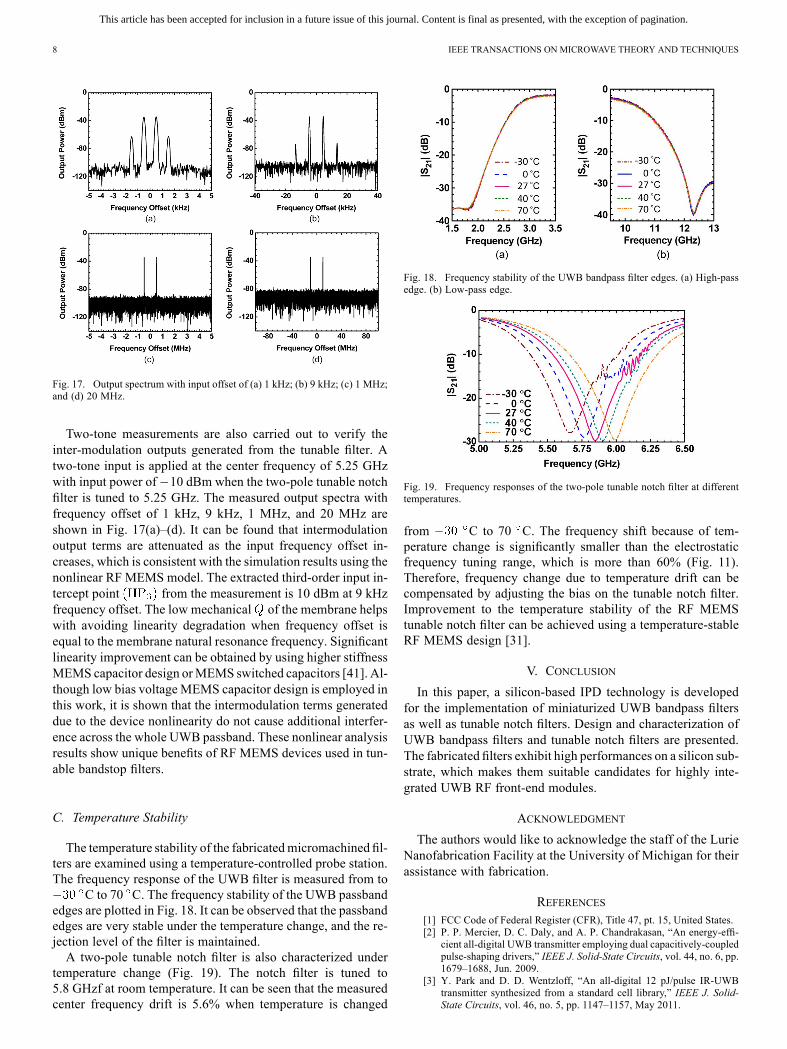
Fig. 17. Output spectrum with input offset of (a) 1 kHz; (b) 9 kHz; (c) 1 MHz;and (d) 20 MHz.
Two-tone measurements are also carried out to verify theinter-modulation outputs generated from the tunable filter. Atwo-tone input is applied at the center frequency of 5.25 GHzwith input power of 10 dBm when the two-pole tunable notchfilter is tuned to 5.25 GHz. The measured output spectra withfrequency offset of 1 kHz, 9 kHz, 1 MHz, and 20 MHz areshown in Fig. 17(a)–(d). It can be found that intermodulationoutput terms are attenuated as the input frequency offset in-creases, which is consistent with the simulation results using thenonlinear RF MEMS model. The extracted third-order input in-tercept point from the measurement is 10 dBm at 9 kHzfrequency offset. The low mechanical of the membrane helpswith avoiding linearity degradation when frequency offset isequal to the membrane natural resonance frequency. Significantlinearity improvement can be obtained by using higher stiffnessMEMS capacitor design orMEMS switched capacitors [41]. Al-though low bias voltageMEMS capacitor design is employed inthis work, it is shown that the intermodulation terms generateddue to the device nonlinearity do not cause additional interfer-ence across the whole UWB passband. These nonlinear analysisresults show unique benefits of RF MEMS devices used in tun-able bandstop filters.
C. Temperature Stability
The temperature stability of the fabricatedmicromachined fil-ters are examined using a temperature-controlled probe station.The frequency response of the UWB filter is measured from to
C to 70 C. The frequency stability of the UWB passbandedges are plotted in Fig. 18. It can be observed that the passbandedges are very stable under the temperature change, and the re-jection level of the filter is maintained.A two-pole tunable notch filter is also characterized under
temperature change (Fig. 19). The notch filter is tuned to5.8 GHzf at room temperature. It can be seen that the measuredcenter frequency drift is 5.6% when temperature is changed
Fig. 18. Frequency stability of the UWB bandpass filter edges. (a) High-passedge. (b) Low-pass edge.
Fig. 19. Frequency responses of the two-pole tunable notch filter at differenttemperatures.
from C to 70 C. The frequency shift because of tem-perature change is significantly smaller than the electrostaticfrequency tuning range, which is more than 60% (Fig. 11).Therefore, frequency change due to temperature drift can becompensated by adjusting the bias on the tunable notch filter.Improvement to the temperature stability of the RF MEMStunable notch filter can be achieved using a temperature-stableRF MEMS design [31].
V. CONCLUSION
In this paper, a silicon-based IPD technology is developedfor the implementation of miniaturized UWB bandpass filtersas well as tunable notch filters. Design and characterization ofUWB bandpass filters and tunable notch filters are presented.The fabricated filters exhibit high performances on a silicon sub-strate, which makes them suitable candidates for highly inte-grated UWB RF front-end modules.
ACKNOWLEDGMENT
The authors would like to acknowledge the staff of the LurieNanofabrication Facility at the University of Michigan for theirassistance with fabrication.
REFERENCES[1] FCC Code of Federal Register (CFR), Title 47, pt. 15, United States.[2] P. P. Mercier, D. C. Daly, and A. P. Chandrakasan, “An energy-effi-
cient all-digital UWB transmitter employing dual capacitively-coupledpulse-shaping drivers,” IEEE J. Solid-State Circuits, vol. 44, no. 6, pp.1679–1688, Jun. 2009.
[3] Y. Park and D. D. Wentzloff, “An all-digital 12 pJ/pulse IR-UWBtransmitter synthesized from a standard cell library,” IEEE J. Solid-State Circuits, vol. 46, no. 5, pp. 1147–1157, May 2011.

This article has been accepted for inclusion in a future issue of this journal. Content is final as presented, with the exception of pagination.
WU et al.: MINIATURIZED UWB FILTERS INTEGRATED WITH TUNABLE NOTCH FILTERS 9
[4] F. S. Lee and A. P. Chandrakasan, “A 2.5 nJ/bit 0.65 V pulsed UWBreceiver in 90 nm CMOS,” IEEE J. Solid-State Circuits, vol. 42, no.12, pp. 2851–2859, Dec. 2007.
[5] F. Zhang, A. Jha, R. Gharpurey, and P. Kinget, “An agile, ultra-wide-band pulse radio transceiver with discrete-time wideband-IF,” IEEE J.Solid-State Circuits, vol. 44, no. 5, pp. 1336–1351, May 2009.
[6] T. Kikkawa, P. K. Saha, N. Sasaki, and K. Kimoto, “Gaussian mono-cycle pulse transmitter using 0.18 CMOS technology with on-chipintegrated antennas for inter-chip UWB communication,” IEEE J.Solid-State Circuits, vol. 43, no. 5, pp. 1303–1312, May 2008.
[7] A. Vallese, A. Bevilacqua, C. Sandner, M. Tiebout, A. Gerosa, and A.Neviani, “Analysis and design of an integrated notch filter for the re-jection of interference in UWB systems,” IEEE J. Solid-State Circuits,vol. 44, no. 2, pp. 331–343, Feb. 2009.
[8] G. Cusmai,M. Brandolini, P. Rossi, and F. Svelto, “A 0.18- CMOSselective receiver front-end for UWB applications,” IEEE J. Solid-State Circuits, vol. 41, no. 8, pp. 1764–1771, Aug. 2006.
[9] A. Medi and W. Namgoong, “A high data-rate energy-efficient inter-ference-tolerant fully integrated CMOS frequency channelized UWBtransceiver for impulse radio,” IEEE J. Solid-State Circuits, vol. 43,no. 4, pp. 974–980, Apr. 2008.
[10] R. Roovers, D. M. W. Leenaerts, J. Bergervoet, K. S. Harish, R. C. H.van de Beek, G. van der Weide, H. Waite, Y. Zhang, S. Aggarwal, andC. Razzell, “An interference-robust receiver for ultra-wideband radioin SiGe BiCMOS technology,” IEEE J. Solid-State Circuits, vol. 40,no. 12, pp. 2563–2572, Dec. 2005.
[11] T. Norimatsu, R. Fujiwara, M. Kokubo, M. Miyazaki, A. Maeki, Y.Ogata, S. Kobayashi, N. Koshizuka, and K. Sakamura, “A UWB-IRtransmitter with digitally controlled pulse generator,” IEEE J. Solid-State Circuits, vol. 42, no. 6, pp. 1300–1309, Jun. 2007.
[12] Z. C. Hao and J. S. Hong, “Ultrawideband filter technologies,” IEEEMicrow. Mag., vol. 11, no. 4, pp. 56–68, Jun. 2010.
[13] H. Liang, K.Wu, and X. Zhang, “Development of packaged ultra-wide-band bandpass filters,” IEEE Trans. Microw. Theory Tech., vol. 58, no.1, pp. 220–228, Jan. 2010.
[14] Y. Chen, S. Chang, C. Wei, Y. Wang, and C. H. Huang, “Packagedultra-wide-band bandpass filter based on inverted-Tmultiple-mode res-onators and inverted-F impedance transformers,” IEEE Microw. Mag.,vol. 11, no. 1, pp. 126–129, Feb. 2010.
[15] Z. C. Hao and J. S. Hong, “UWB bandpass filter Using cascadedminiature high-pass and low-pass filters with multilayer liquid crystalpolymer technology,” IEEE Trans. Microw. Theory Tech., vol. 58, no.4, pp. 941–948, Apr. 2010.
[16] H. Shamanand and J. S. Hong, “Ultra-wideband (UWB) bandpassfilter with embedded band notch structures,” IEEE Microw. WirelessCompon. Lett., vol. 17, no. 3, pp. 193–195, Mar. 2007.
[17] Z. C. Hao and J. S. Hong, “Compact UWB filter with doublenotch-bands using multilayer LCP technology,” IEEE Microw. Wire-less Compon. Lett., vol. 19, no. 8, pp. 500–502, Aug. 2009.
[18] X. Luo, J. G. Ma, K. S. Yeo, and E. P. Li, “Compact ultra-wideband(UWB) bandpass filter with ultra-narrow dual-and quad-notchedbands,” IEEE Trans. Microw. Theory Tech., vol. 59, no. 6, pp.1509–1519, Jun. 2011.
[19] H. R. Arachchige, J. S. Hong, and Z. C. Hao, “UWB bandpass filterwith tunable notch on liquid crystal polymer substrate,” in Asia-PacificMicrow. Conf., Dec. 2008, pp. 1–4.
[20] Z. Wu, Y. Shim, and M. Rais-Zadeh, “Miniaturized UWB bandpassfilters integrated with notch filters using a silicon-based integratedpassive device technology,” in IEEE/MTT-S Int. Microw. Symp., Jun.2011, pp. 1–4.
[21] W. D. Yan and R. R. Mansour, “Compact tunable bandstop filter in-tegrated with large deflected actuators,” in IEEE/MTT-S Int. Microw.Symp., Jun. 2007, pp. 1611–1614.
[22] H. S. Lee, D. H. Choi, and J. B. Yoon, “MEMS-based tunable LC band-stop filter with an ultra-wide continuous tuning range,” IEEE Microw.Wireless Compon. Lett., vol. 19, no. 11, pp. 710–712, Nov. 2009.
[23] E. Lourandakis, M. Schmidt, S. Seitz, and R. Weigel, “Tunable lumpedelement filters with BST thin-film varactors,” in Eur. Microw. Conf.,Oct. 2008, pp. 1691–1694.
[24] I. Reines, S. J. Park, and G. M. Rebeiz, “Compact low-loss tunableX-band bandstop filter with miniature RF-MEMS switches,” IEEETrans. Microw. Theory Tech., vol. 58, no. 7, pp. 1887–1895, Jul. 2010.
[25] C. Musoll-Anguiano, I. Llamas-Garro, Z. Brito-Brito, L. Pradell, andA. Corona-Chavez, “Characterizing a tune all bandstop filter,” in IEEE/MTT-S Int. Microw. Workshop Series on Signal Integrity and High-Speed Interconnects, Feb. 2009, pp. 55–58.
[26] Z. Brito-Brito, I. Llamas-Garro, L. Pradell-Cara, and A. Corona-Chavez, “Microstrip switchable bandstop filter using PIN diodes withprecise frequency and bandwidth control,” in Eur. Microw. Conf., Oct.2008, pp. 1707–1710.
[27] D. R. Jachowski and C. Rauscher, “Frequency-agile bandstop filterwith tunable attenuation,” in IEEE/MTT-S Int. Microw. Symp. Digest,Jun. 2009, pp. 649–652.
[28] B. Smilowitz, “High speed varactor tuned notch filter,” in IEEE/MTT-SInt. Microw. Symp. Digest, June 1985, pp. 531–534.
[29] R. Gharpurey and P. Kinget, Ultra Wideband: Circuits, Transceiversand Systems. Boston, MA: Springer, 2008, pp. 60–61.
[30] T. G. S. M. Rijks et al., “Micro-electro-mechanical tunable capacitorsfor reconfigurable RF architectures,” J. Micromech. Microeng., vol. 16,no. 3, pp. 601–611, Mar. 2006.
[31] Y. Shim, Z. Wu, and M. Rais-Zadeh, “A high-performance tempera-ture-stable continuously tuned MEMS capacitor,” in IEEE Int. Conf.Microelectromech. Syst. (MEMS’11), Cancun, Mexico, 2011, pp.752–755.
[32] C. D. Patel and G. M. Rebeiz, “An RF-MEMS switch with mN con-tact forces,” in IEEE/MTT-S Int. Microw. Symp. Digest, May 2010, pp.1242–1245.
[33] “HFSS 1”. Ansoft Corporation, Pittsburgh, PA, 2009.[34] J. D. Rhodes and S. A. Alseyab, “The generalized Chebyshev low-pass
prototype filter,” Int. J. Circuit Theory Appl., vol. 8, no. 4, pp. 113–125,Apr. 1980.
[35] C. W. Tang and D. L. Yang, “Realization of multilayered wide-pass-band bandpass filter with low-temperature co-fired ceramic tech-nology,” IEEE Trans. Microw. Theory Tech., vol. 56, no. 7, pp.1668–1674, Jul. 2008.
[36] S. S. Mohan, C. P. Yue, M. del Mar Hershenson, S. S. Wong, and T. H.Lee, “Modeling and characterization of on-chip transformers,” in Int.Electron Devices Meeting, Dec. 1998, pp. 531–534.
[37] B. M. Schiffman and G. L. Matthaei, “Exact design of band-stop mi-crowave filters,” IEEE Trans. Microw. Theory Tech., vol. 12, no. 1, pp.6–15, Jan. 1964.
[38] D. M. Pozar, Microwave Engineering. Hoboken, NJ: Wiley, 2005.[39] J. Hogerheiden, M. Ciminera, and G. Jue, “Improved planar spiral
transformer theory applied to a miniature lumped element quadra-ture hybrid,” IEEE Trans. Microw. Theory Tech., vol. 45, no. 4, pp.543–545, Apr. 1997.
[40] A. Cruau, P. Nicole, G. Lissorgues, and C. M. Tassetti, “Influence ofRF signal power on tunable MEMS capacitors,” in Eur. Microw. Conf.,Oct. 2003, vol. 2, pp. 663–666.
[41] G. M. Rebeiz, RF MEMS: Theory, Design, and Technology.Hoboken, NJ: Wiley, 2003.
[42] L. Dussopt and G. M. Rebeiz, “Intermodulation distortion and powerhandling in RF MEMS switches, varactors, and tunable filters,” IEEETrans. Microw. Theory Tech., vol. 51, no. 4, pp. 1247–1256, Apr. 2003.
[43] “Advanced Design System 2009A”. Agilent Technol. Inc., Palo Alto,CA, 2009.
Zhengzheng Wu (S’09) received the B.S. degree inmicroelectronics from Fudan University, Shanghai,China, in 2005, and the M.S. degree in microelec-tronics from the Shanghai Institute of Microsystemand Information Technology, Chinese Academy ofSciences, Shanghai, China, in 2009. Currently, he isworking towards the Ph.D. degree in electrical en-gineering and computer science at the University ofMichigan, Ann Arbor.During the summer of 2011, he was an Intern with
Samsung Telecommunications America, Dallas, TX,where he was involved in developing multiband RF power amplifiers for wire-less handsets. His research interests include MEMS for wireless applicationsand timing references, tunable RF filters and passive circuits, circuits for wire-less transceivers, and integrated Microsystems.Mr. Wu received the Rackham International Student Fellowship from the
University of Michigan for 2010–2011. He was a student paper competitionfinalist at the 2011 International Microwave Symposium.

This article has been accepted for inclusion in a future issue of this journal. Content is final as presented, with the exception of pagination.
10 IEEE TRANSACTIONS ON MICROWAVE THEORY AND TECHNIQUES
Yonghyun Shim (S’09) received the B.S. degree inelectrical engineering from Seoul National Univer-sity, Seoul, Korea, in 2007, and the M.S.E. degreein electrical engineering and computer science fromthe University of Michigan, Ann Arbor, in 2009.Currently, he is working towards the Ph.D. degreein electrical engineering and computer science at theUniversity of Michigan, Ann Arbor.His research interests include micromachined RF
front-end filters, RF MEMS passives, RF IC andwireless front-end, and CMOS-MEMS integration.
Mina Rais-Zadeh (S’03–M’08) received the B.S.degree in electrical engineering from the SharifUniversity of Technology ,Tehran, Iran, and theM.S. and Ph.D. degrees in electrical and computerengineering from Georgia Institute of Technology,Atlanta, in 2005 and 2008, respectively.From August 2008 to 2009, she was a Postdoctoral
Research Fellow with the Integrated MEMS Group,Georgia Institute of Technology. Since January2009, she has been with the University of Michigan,Ann Arbor, where she is currently an Assistant Pro-
fessor in the Department of Electrical Engineering and Computer Science. Herresearch interests include passive micromachined devices for communicationapplications, resonant micromechanical devices, gallium nitride MEMS, andmicro/nano fabrication process development.Prof. Rais-Zadeh is the recipient of the NSF CAREER Award (2011), the
IEEE Electron Device Society Early Career Award (2011), and finalist in thestudent paper competitions at the SiRF (2007) and IMS (2011) conferences.She serves as a member of the technical program committee of IEEE IEDM,IEEE Sensors, and Hilton Head workshop.


![(1982) Test-Score Semantics for Natural Languages [Zadeh]](https://img.dokumen.tips/doc/110x75/577cc89d1a28aba711a31882/1982-test-score-semantics-for-natural-languages-zadeh.jpg)