Embed Size (px)
Citation preview
preliminary
preliminary iC-MB4BiSS INTERFACE MASTER
Rev C1, Page 1/42
FEATURES
Bidirectional BiSS communication with up to 8 slaves Supports SSI protocol for unidirectional data transmission Synchronous sensor data acquisition with cyclic transfer at data
rates of up to 10 Mbit/s Configurable interface with TTL, CMOS, RS422 or LVDS Slave register operations during cyclic data transfers Automatic compensation of line delays and conversion times Data lengths of up to 64 bit for sensor data,
configurable for each slave Data verification by CRC polynomials of up to 16 bits per slave Separate memory banks enable free controller access during
BiSS sensor data transfers 64 bytes memory for bidirectional register communication Serial controller communication by SPITM-compatible mode Parallel interface with 8 bit data/address bus for Intel- and
Motorola-devices with combined data and address bus Single 3 V to 5 V supply, industrial temperature range
APPLICATIONS
Bidirectional communication inmulti sensor systems
Linear and rotary encoders Motor feedback systems PLC systems Drives
PACKAGES
QFN285 mm x 5 mm
RoHS compliant
TSSOP24
BLOCK DIAGRAM
VDD
PROCESS DATA
OSCILLATOR
HOST INTERFACE RESET
CTRL PORTS
BANK 3
BiSS INTERFACE
VDD
VDD
INSTANCE 3
BANK v
sample CDSmeasure busy
FRAME CONTROLLER
send busy
request sensor datasend acknowledge
DATABUS
ADDRESSBUS
W W
CHANNEL 3
iC6MBf
analyse wire delay
INSTANCE v
CHANNEL v
3_ BYTE RAM
PARAMETER
CONTROL
CONFIG
PROCESS
f x hv BIT RAM
DATA
DATA
PROCESS
f x _f BIT RAM
CONTROLLER
calculate actuator crcsend actuator datareceive sensor datacheck sensor data
_f BYTE RAM
send startcalculate control frame
send CDM
GND
NCS
MO3
DB5
INT_NMOT
SLv_NSL3
MOv_NMO3
DB7
NRES
DB_
CLK
VDD
NWR_E
DBf
EOT
NER
GETSENSDBv
DB3
DBx
NRD_RNW
CFGSPI
DBh
ALE
MAv_NMA3
MA3
SL3
Copyright © 2014, 2018 iC-Haus http://www.ichaus.com
preliminary
preliminary iC-MB4BiSS INTERFACE MASTER
Rev C1, Page 2/42
DESCRIPTION
iC-MB4 is a single-chip BiSS/SSI interface mastercontroller featuring an 8-bit bus interface to industrialstandard microcontroller. Alternatively an SPI inter-face enables serial communication between iC-MB4and the connected microcontroller. The BiSS devicesincluding one or several sensors are connected to theclock line MA and the data return line SL via point-to-point connection (Figure 1). The BiSS devices includ-ing actuators and sensors are additionally connectedto the data line MO. It is possible to connect multi-ple devices in chain (Figure 2). RS422 transceiversare used in industrial environments. A maximum ofeight BiSS slaves are supported, each with it’s ownconfigurable data sections covering:
1. Sensor / actuator data from 0 to 64 bits(for measurement data, flags like alarm andwarning, Sign of Life cycle counter, . . . )
2. Register data with 64 directly addressable bytesand 256 banks with 64 bytes per slave ID(e.g. for device parameters)
iC-MB4 provides two RAM memory banks for eachslave enabling simultaneous access by the microcon-troller while new sensor data is being read. A 64-bytememory supports register transfers. Sensor dataacquisition is started by a microcontroller commandor via pin GETSENS. Alternatively, iC-MB4 can alsoread new sensor data automatically. In this case thecycle time can be set as required. The end of the
sensor data acquisition and transmission is indicatedat the pin EOT. In case of an error during transmis-sion the pin NER signals a digital low. Errors duringcommunication can be verified by the microcontrollervia a status register. A system error message canalso access this register if the bidirectional messagepin NER is kept digital low by an external interven-tion. iC-MB4 generates a clock signal for sensorcommunication using an internal 20 MHz oscillator.The clock can also be supplied externally. iC-MB4is based on the BiSS master IP family MB100_X.
controldata
Device1(Sensor)Master
clock/
LastSlave
controldata
ID1..N-1
ID0
sensordata/
MA+MA-
SL-
V-
V+
SL+
MA-MA+
SLO-SLO+
Figure 1: Point-to-point connection of iC-MB4 toone device with several slaves
controldata
actuatordata IDN
IDN+1..M-1
LastSlave
ID0
ID1..N-1
Device2(Sensor/Actuator) Device1(Sensor/Actuator)Master
clock/controldata
sensordata/
MA-MA+
V-
V+
SLI+SLI-
MA+MA-
SL+SL-SL-
SL+
MO+MO-
MAO-MAO+
SLO+SLO-
SLR-
MO-MO+
V-
V+
MA+MA-
SL+SL-
SLR+
Figure 2: Example network of iC-MB4 and two devicesThe device offered here is a multifunctional iC that contains integrated BiSS C interface components. The BiSS C process is protectedby patent DE 10310622 B4 owned by iC-Haus GmbH. Users benefit from the open BiSS C protocol with a free license which isnecessary when using the BiSS C protocol in conjunction with this iC.Download the license at www.biss-interface.com/BUA
preliminary
preliminary iC-MB4BiSS INTERFACE MASTER
Rev C1, Page 3/42
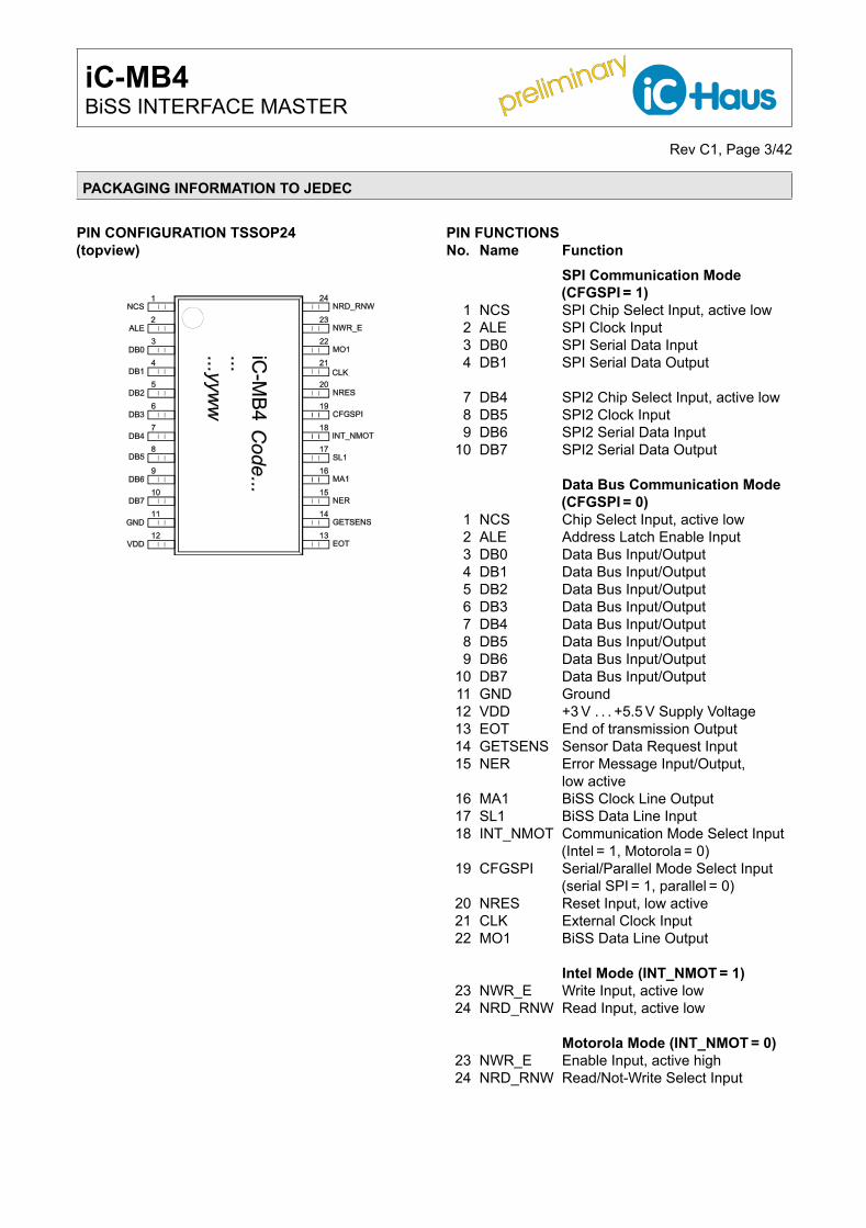
PACKAGING INFORMATION TO JEDEC
PIN CONFIGURATION TSSOP24(topview)
PIN FUNCTIONSNo. Name Function
SPI Communication Mode(CFGSPI = 1)
1 NCS SPI Chip Select Input, active low2 ALE SPI Clock Input3 DB0 SPI Serial Data Input4 DB1 SPI Serial Data Output
7 DB4 SPI2 Chip Select Input, active low8 DB5 SPI2 Clock Input9 DB6 SPI2 Serial Data Input
10 DB7 SPI2 Serial Data Output
Data Bus Communication Mode(CFGSPI = 0)
1 NCS Chip Select Input, active low2 ALE Address Latch Enable Input3 DB0 Data Bus Input/Output4 DB1 Data Bus Input/Output5 DB2 Data Bus Input/Output6 DB3 Data Bus Input/Output7 DB4 Data Bus Input/Output8 DB5 Data Bus Input/Output9 DB6 Data Bus Input/Output
10 DB7 Data Bus Input/Output11 GND Ground12 VDD +3 V . . . +5.5 V Supply Voltage13 EOT End of transmission Output14 GETSENS Sensor Data Request Input15 NER Error Message Input/Output,
low active16 MA1 BiSS Clock Line Output17 SL1 BiSS Data Line Input18 INT_NMOT Communication Mode Select Input
(Intel = 1, Motorola = 0)19 CFGSPI Serial/Parallel Mode Select Input
(serial SPI = 1, parallel = 0)20 NRES Reset Input, low active21 CLK External Clock Input22 MO1 BiSS Data Line Output
Intel Mode (INT_NMOT = 1)23 NWR_E Write Input, active low24 NRD_RNW Read Input, active low
Motorola Mode (INT_NMOT = 0)23 NWR_E Enable Input, active high24 NRD_RNW Read/Not-Write Select Input
preliminary
preliminary iC-MB4BiSS INTERFACE MASTER
Rev C1, Page 4/42
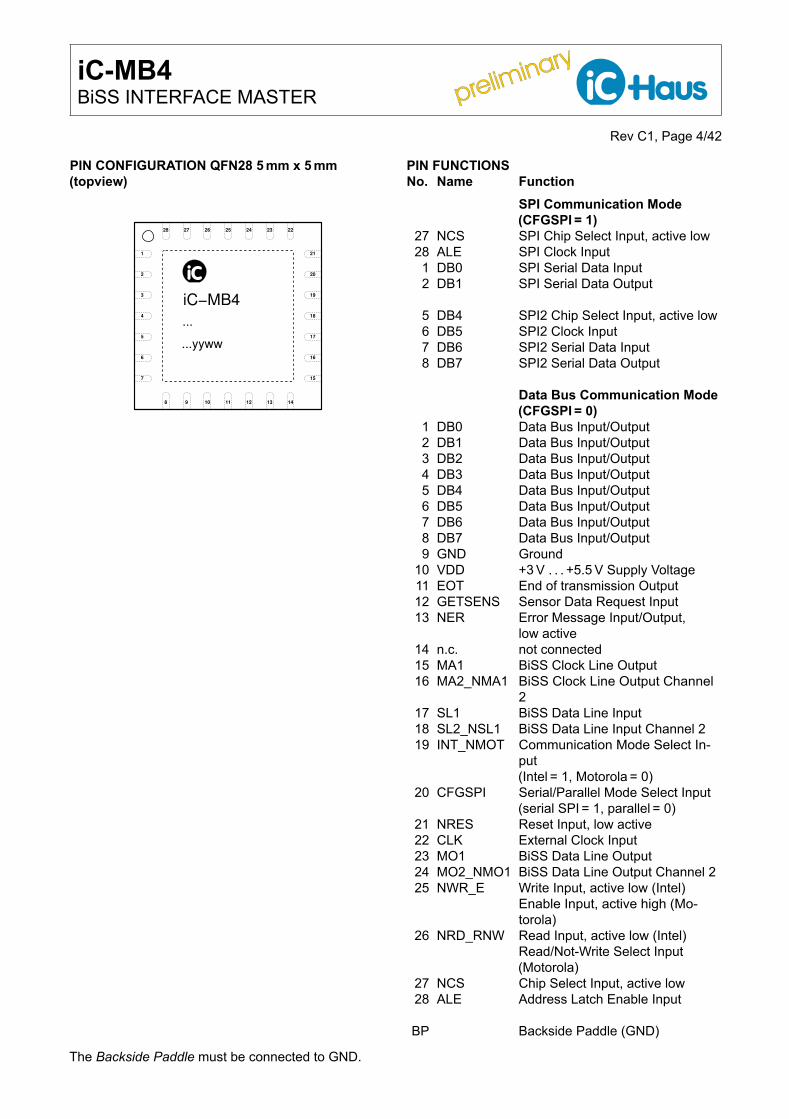
PIN CONFIGURATION QFN28 5 mm x 5 mm(topview)
...
...yyww
iC−MB4
15
16
17
18
19
20
21
232425262728 22
1
2
3
4
5
6
7
8 9 10 11 12 13 14
PIN FUNCTIONSNo. Name Function
SPI Communication Mode(CFGSPI = 1)
27 NCS SPI Chip Select Input, active low28 ALE SPI Clock Input
1 DB0 SPI Serial Data Input2 DB1 SPI Serial Data Output
5 DB4 SPI2 Chip Select Input, active low6 DB5 SPI2 Clock Input7 DB6 SPI2 Serial Data Input8 DB7 SPI2 Serial Data Output
Data Bus Communication Mode(CFGSPI = 0)
1 DB0 Data Bus Input/Output2 DB1 Data Bus Input/Output3 DB2 Data Bus Input/Output4 DB3 Data Bus Input/Output5 DB4 Data Bus Input/Output6 DB5 Data Bus Input/Output7 DB6 Data Bus Input/Output8 DB7 Data Bus Input/Output9 GND Ground
10 VDD +3 V . . . +5.5 V Supply Voltage11 EOT End of transmission Output12 GETSENS Sensor Data Request Input13 NER Error Message Input/Output,
low active14 n.c. not connected15 MA1 BiSS Clock Line Output16 MA2_NMA1 BiSS Clock Line Output Channel
217 SL1 BiSS Data Line Input18 SL2_NSL1 BiSS Data Line Input Channel 219 INT_NMOT Communication Mode Select In-
put(Intel = 1, Motorola = 0)
20 CFGSPI Serial/Parallel Mode Select Input(serial SPI = 1, parallel = 0)
21 NRES Reset Input, low active22 CLK External Clock Input23 MO1 BiSS Data Line Output24 MO2_NMO1 BiSS Data Line Output Channel 225 NWR_E Write Input, active low (Intel)
Enable Input, active high (Mo-torola)
26 NRD_RNW Read Input, active low (Intel)Read/Not-Write Select Input(Motorola)
27 NCS Chip Select Input, active low28 ALE Address Latch Enable Input
BP Backside Paddle (GND)
The Backside Paddle must be connected to GND.
preliminary
preliminary iC-MB4BiSS INTERFACE MASTER
Rev C1, Page 5/42
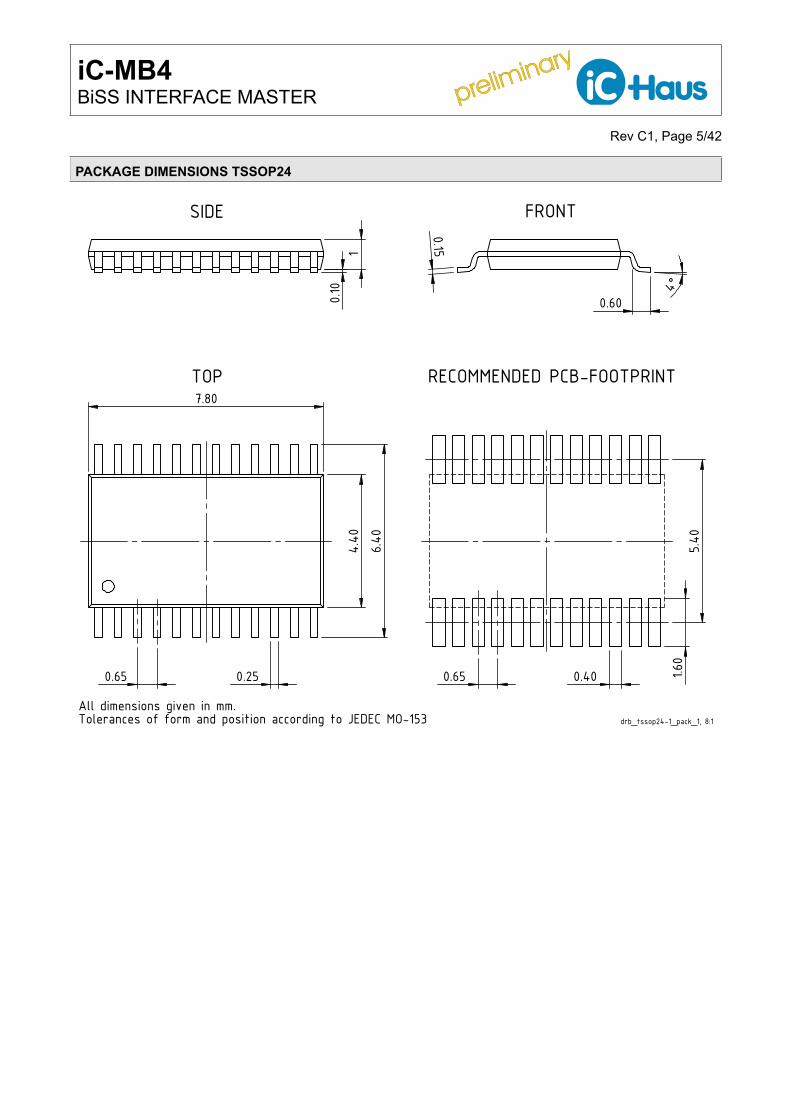
PACKAGE DIMENSIONS TSSOP24
0.65
7.80
4.40
6.40
0.25
TOP1
0.10
SIDE
0.15
0.60
4°
FRONT
5.400.400.65 1.6
0
RECOMMENDED PCB-FOOTPRINT
drb_tssop24-1_pack_1, 8:1
All dimensions given in mm. Tolerances of form and position according to JEDEC MO-153
preliminary
preliminary iC-MB4BiSS INTERFACE MASTER
Rev C1, Page 6/42
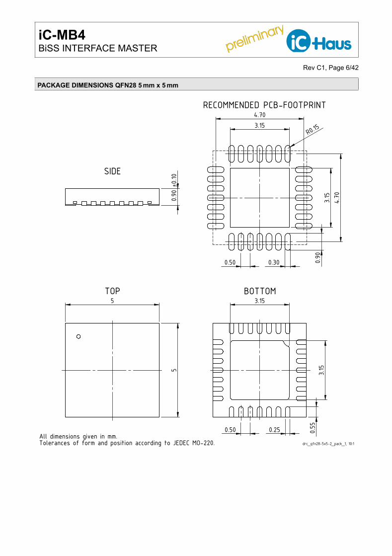
PACKAGE DIMENSIONS QFN28 5 mm x 5 mm
5
5
TOP
0.250.50
3.15
3.15
0.55
BOTTOM
0.90
±0.10
SIDE
4.70
3.15
4.70
0.50
R0.153.15
0.90
0.30
RECOMMENDED PCB-FOOTPRINT
drc_qfn28-5x5-2_pack_1, 10:1All dimensions given in mm. Tolerances of form and position according to JEDEC MO-220.
preliminary
preliminary iC-MB4BiSS INTERFACE MASTER
Rev C1, Page 7/42
ABSOLUTE MAXIMUM RATINGS
Beyond these values damage may occur; device operation is not guaranteed.Item Symbol Parameter Conditions UnitNo. Min. Max.G001 VDD Voltage at VDD -0.3 6 VG002 I(VDD) Current in VDD -20 30 mAG003 V() Voltage at all pins excluding VDD and
GNDV() VDD + 0.3 V -0.3 6 V
G004 I() Current in all pins excluding VDD andGND
-10 10 mA
G005 Vesd() ESD Susceptibility at all pins HBM, 100 pF discharged through 2 kV1.5 Ω
G006 Tj Operating Junction Temperature VDD = 3.0 V ... 4.5 V -40 125 °CVDD = 4.5 V ... 5.5 V -40 140 °C
G007 Ts Storage Temperature Range -40 150 °C
THERMAL DATA
Operating Conditions: VDD = 3.0 V. . . 5.5 VItem Symbol Parameter Conditions UnitNo. Min. Typ. Max.
T01 Ta Standard Operating AmbientTemperature Range
-40 85 °C
T02 TaET Extended Operating AmbientTemperature Range
VDD = 4.5 V ... 5.5 V -40 125 °C
available on requestT03 RthjaTSSOP Thermal Resistance Chip to Ambient TSSOP24 surface mounted,
no special heat sink80 K/W
T04 RthjaQFN Thermal Resistance Chip to Ambient QFN28 package mounted on PCB,Backside Paddle at approx. 2 cm² cooling area
40 K/W
All voltages are referenced to ground unless otherwise stated.All currents flowing into the device pins are positive; all currents flowing out of the device pins are negative.
preliminary
preliminary iC-MB4BiSS INTERFACE MASTER
Rev C1, Page 8/42
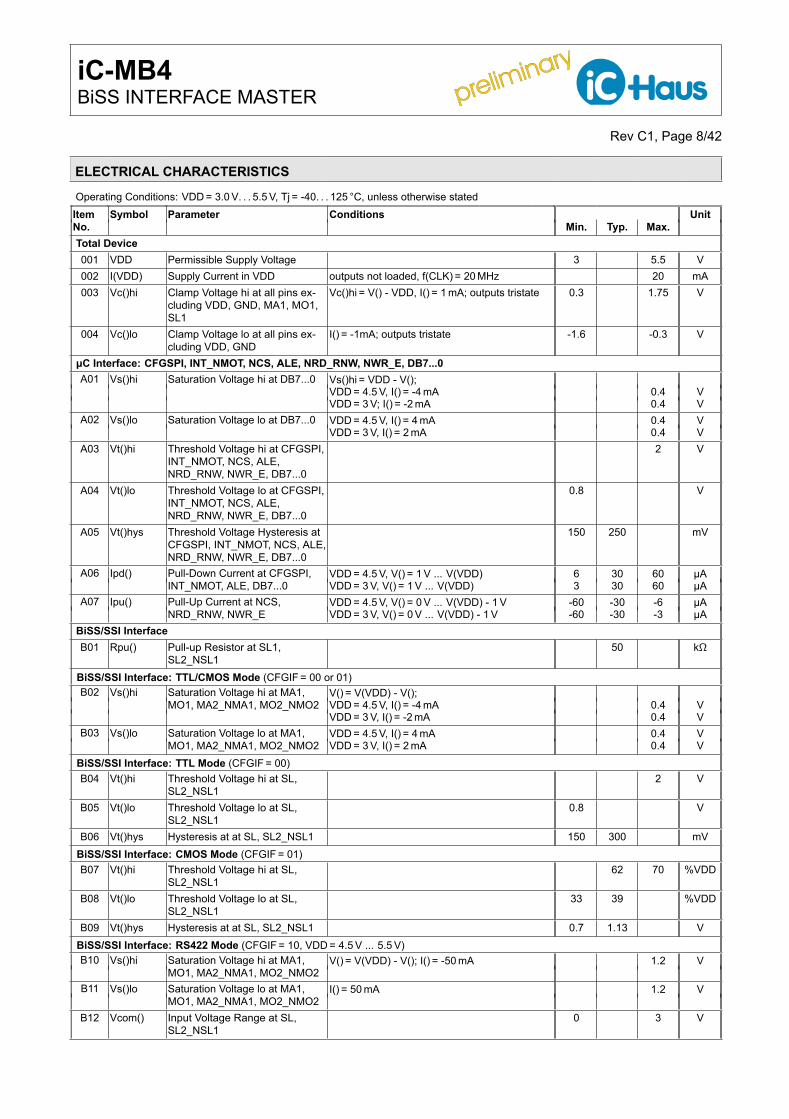
ELECTRICAL CHARACTERISTICS
Operating Conditions: VDD = 3.0 V. . . 5.5 V, Tj = -40. . . 125 °C, unless otherwise statedItem Symbol Parameter Conditions UnitNo. Min. Typ. Max.Total Device001 VDD Permissible Supply Voltage 3 5.5 V002 I(VDD) Supply Current in VDD outputs not loaded, f(CLK) = 20 MHz 20 mA003 Vc()hi Clamp Voltage hi at all pins ex-
cluding VDD, GND, MA1, MO1,SL1
Vc()hi = V() - VDD, I() = 1 mA; outputs tristate 0.3 1.75 V
004 Vc()lo Clamp Voltage lo at all pins ex-cluding VDD, GND
I() = -1mA; outputs tristate -1.6 -0.3 V
µC Interface: CFGSPI, INT_NMOT, NCS, ALE, NRD_RNW, NWR_E, DB7...0A01 Vs()hi Saturation Voltage hi at DB7...0 Vs()hi = VDD - V();
VDD = 4.5 V, I() = -4 mA 0.4 VVDD = 3 V; I() = -2 mA 0.4 V
A02 Vs()lo Saturation Voltage lo at DB7...0 VDD = 4.5 V, I() = 4 mA 0.4 VVDD = 3 V, I() = 2 mA 0.4 V
A03 Vt()hi Threshold Voltage hi at CFGSPI,INT_NMOT, NCS, ALE,NRD_RNW, NWR_E, DB7...0
2 V
A04 Vt()lo Threshold Voltage lo at CFGSPI,INT_NMOT, NCS, ALE,NRD_RNW, NWR_E, DB7...0
0.8 V
A05 Vt()hys Threshold Voltage Hysteresis atCFGSPI, INT_NMOT, NCS, ALE,NRD_RNW, NWR_E, DB7...0
150 250 mV
A06 Ipd() Pull-Down Current at CFGSPI,INT_NMOT, ALE, DB7...0
VDD = 4.5 V, V() = 1 V ... V(VDD) 6 30 60 µAVDD = 3 V, V() = 1 V ... V(VDD) 3 30 60 µA
A07 Ipu() Pull-Up Current at NCS,NRD_RNW, NWR_E
VDD = 4.5 V, V() = 0 V ... V(VDD) - 1 V -60 -30 -6 µAVDD = 3 V, V() = 0 V ... V(VDD) - 1 V -60 -30 -3 µA
BiSS/SSI InterfaceB01 Rpu() Pull-up Resistor at SL1,
SL2_NSL150 kΩ
BiSS/SSI Interface: TTL/CMOS Mode (CFGIF = 00 or 01)B02 Vs()hi Saturation Voltage hi at MA1,
MO1, MA2_NMA1, MO2_NMO2V() = V(VDD) - V();VDD = 4.5 V, I() = -4 mA 0.4 VVDD = 3 V, I() = -2 mA 0.4 V
B03 Vs()lo Saturation Voltage lo at MA1,MO1, MA2_NMA1, MO2_NMO2
VDD = 4.5 V, I() = 4 mA 0.4 VVDD = 3 V, I() = 2 mA 0.4 V
BiSS/SSI Interface: TTL Mode (CFGIF = 00)B04 Vt()hi Threshold Voltage hi at SL,
SL2_NSL12 V
B05 Vt()lo Threshold Voltage lo at SL,SL2_NSL1
0.8 V
B06 Vt()hys Hysteresis at at SL, SL2_NSL1 150 300 mVBiSS/SSI Interface: CMOS Mode (CFGIF = 01)B07 Vt()hi Threshold Voltage hi at SL,
SL2_NSL162 70 %VDD
B08 Vt()lo Threshold Voltage lo at SL,SL2_NSL1
33 39 %VDD
B09 Vt()hys Hysteresis at at SL, SL2_NSL1 0.7 1.13 VBiSS/SSI Interface: RS422 Mode (CFGIF = 10, VDD = 4.5 V ... 5.5 V)B10 Vs()hi Saturation Voltage hi at MA1,
MO1, MA2_NMA1, MO2_NMO2V() = V(VDD) - V(); I() = -50 mA 1.2 V
B11 Vs()lo Saturation Voltage lo at MA1,MO1, MA2_NMA1, MO2_NMO2
I() = 50 mA 1.2 V
B12 Vcom() Input Voltage Range at SL,SL2_NSL1
0 3 V
preliminary
preliminary iC-MB4BiSS INTERFACE MASTER
Rev C1, Page 9/42
ELECTRICAL CHARACTERISTICS
Operating Conditions: VDD = 3.0 V. . . 5.5 V, Tj = -40. . . 125 °C, unless otherwise statedItem Symbol Parameter Conditions UnitNo. Min. Typ. Max.
B13 Vtdiff() Threshold Voltage atSL - SL2_NSL1
V()=V(P) - V(N) -300 300 mV
B14 Vthys() Hysteresis Voltage atSL - SL2_NSL1
V()=V(P) - V(N) 75 150 mV
BiSS/SSI Interface: LVDS Mode (CFGIF = 11)B15 Vs()hi Output Voltage hi at MA1, MO1,
MA2_NMA1, MO2_NMO2RL = 100ΩVDD = 4.5 V ... 5.5 V 1.25 1.6 VVDD = 3.0 V ... 3.6 V 1.0 1.6 V
B16 Vs()lo Output Voltage lo at MA1, MO1,MA2_NMA1, MO2_NMO2
RL = 100ΩVDD = 4.5 V ... 5.5 V 0.9 1.125 VVDD = 3.0 V ... 3.6 V 0.7 1.125 V
B17 Vadiff Differential Output Voltage atMA1 - MA2_NMA1,MO1 - MO2_NMO2
RL = 100ΩVDD = 4.5 V ... 5.5 V 250 350 450 mVVDD = 3.0 V ... 3.6 V 220 350 450 mV
B18 Vacm Common Mode Output Voltage loat MA1, MO1, MA2_NMA1,MO2_NMO2
RL = 100ΩVDD = 4.5 V ... 5.5 V 1.125 1.2 1.375 VVDD = 3.0 V ... 3.6 V 0.9 1.15 1.375 V
B19 Vcom() Input Voltage Range at SL,SL2_NSL1
VDD = 4.5 V ... 5.5 V 0.8 3 VVDD = 3.0 V ... 3.6 V 0.8 1.8 V
B20 Vtdiff() Threshold Voltage atSL - SL2_NSL1
V()=V(P) - V(N) -150 150 mV
B21 Vthys() Hysteresis Voltage atSL - SL2_NSL1
V()=V(P) - V(N)VDD = 4.5 V ... 5.5 V 25 70 mVVDD = 3.0 V ... 3.6 V 14 40 mV
I/O Ports: EOT, NER, GETSENSC01 Vs()hi Saturation Voltage hi at EOT Vs()hi = VDD - V();
VDD = 4.5 V, I() = -4 mA 0.4 VVDD = 3 V; I() = -2 mA 0.4 V
C02 Vs()lo Saturation Voltage lo at EOT,NER
VDD = 4.5 V, I() = 4 mA 0.4 VVDD = 3 V, I() = 2 mA 0.4 V
C03 Vt()hi Threshold Voltage hi at NER,GETSENS
2 V
C04 Vt()lo Threshold Voltage lo at NER,GETSENS
0.8 V
C05 Vt()hys Threshold Voltage Hysteresis atNER, GETSENS
150 250 mV
C06 Ipd() Pull-Down Current at GETSENS VDD = 4.5 V, V() = 1 V ... V(VDD) 6 30 60 µAVDD = 3 V, V() = 1 V ... V(VDD) 3 30 60 µA
C07 Ipu() Pull-Up Current at NER V() = 0 V ... V(VDD) - 1 V -950 -300 -35 µAC08 Tw(GETSENS)
Minimum duration of GETSENSpulse
1/f(CLK)
Oscillator: CLKD01 f(CLK) Permissible external Clock Rate
at CLKDuty cycle 48% . . . 52% 20 25 MHz
D02 Vt(CLK)hi Threshold Voltage hi 2 VD03 Vt(CLK)lo Threshold Voltage lo 0.4 VD04 Vt(CLK)hys Threshold Voltage Hysteresis 150 250 mVD05 f(CLKI) Internal Oscillator Clock
FrequencyVDD = 4.5 V ... 5.5 V 15 20 25 MHzVDD = 3.0 V ... 3.6 V 10 15 22 MHz
D06 Ipd() Pull-Down Current at CLK VDD = 4.5 V, V() = 1.5 V ... VDD 6 30 60 µAVDD = 3 V, V() = 1.5 V ... VDD 3 30 60 µA
preliminary
preliminary iC-MB4BiSS INTERFACE MASTER
Rev C1, Page 10/42
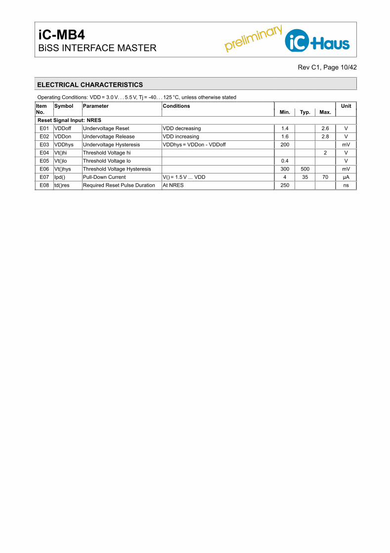
ELECTRICAL CHARACTERISTICS
Operating Conditions: VDD = 3.0 V. . . 5.5 V, Tj = -40. . . 125 °C, unless otherwise statedItem Symbol Parameter Conditions UnitNo. Min. Typ. Max.Reset Signal Input: NRESE01 VDDoff Undervoltage Reset VDD decreasing 1.4 2.6 VE02 VDDon Undervoltage Release VDD increasing 1.6 2.8 VE03 VDDhys Undervoltage Hysteresis VDDhys = VDDon - VDDoff 200 mVE04 Vt()hi Threshold Voltage hi 2 VE05 Vt()lo Threshold Voltage lo 0.4 VE06 Vt()hys Threshold Voltage Hysteresis 300 500 mVE07 Ipd() Pull-Down Current V() = 1.5 V ... VDD 4 35 70 µAE08 td()res Required Reset Pulse Duration At NRES 250 ns
preliminary
preliminary iC-MB4BiSS INTERFACE MASTER
Rev C1, Page 11/42
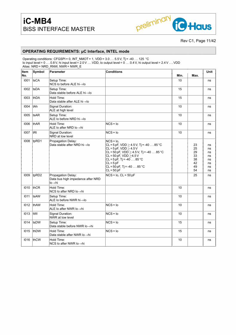
OPERATING REQUIREMENTS: µC Interface, INTEL mode
Operating conditions: CFGSPI = 0, INT_NMOT = 1, VDD = 3.0 . . . 5.5 V, Tj = -40 . . . 125 °Clo input level = 0 . . . 0.8 V, hi input level = 2.0 V . . . VDD, lo output level = 0 . . . 0.4 V, hi output level = 2.4 V . . . VDDAlias: NRD = NRD_RNW, NWR = NWR_EItem Symbol Parameter Conditions UnitNo. Min. Max.
I001 tsCA Setup Time:NCS lo before ALE hi→lo
10 ns
I002 tsDA Setup Time:Data stable before ALE hi→lo
15 ns
I003 thDA Hold Time:Data stable after ALE hi→lo
15 ns
I004 tAh Signal Duration:ALE at high level
10 ns
I005 tsAR Setup Time:ALE lo before NRD hi→lo
10 ns
I006 thAR Hold Time:ALE lo after NRD lo→hi
NCS = lo 10 ns
I007 tRl Signal Duration:NRD at low level
NCS = lo 10 ns
I008 tpRD1 Propagation Delay:Data stable after NRD hi→lo
NCS = lo,CL = 5 pF, VDD≥ 4.5 V, Tj = -40 . . . 85 °C 23 nsCL = 5 pF, VDD≥ 4.5 V 25 nsCL = 50 pF, VDD≥4.5 V, Tj = -40 . . . 85 °C 29 nsCL = 50 pF, VDD≥4.5 V 33 nsCL = 5 pF, Tj = -40 . . . 85 °C 38 nsCL = 5 pF 42 nsCL = 50 pF, Tj = -40 . . . 85 °C 49 nsCL = 50 pF 54 ns
I009 tpRD2 Propagation Delay:Data bus high impedance after NRDlo→hi
NCS = lo, CL = 50 pF 25 ns
I010 thCR Hold Time:NCS lo after NRD lo→hi
10 ns
I011 tsAW Setup Time:ALE lo before NWR hi→lo
10 ns
I012 thAW Hold Time:ALE lo after NWR lo→hi
NCS = lo 10 ns
I013 tWl Signal Duration:NWR at low level
NCS = lo 10 ns
I014 tsDW Setup Time:Data stable before NWR lo→hi
NCS = lo 15 ns
I015 thDW Hold Time:Data stable after NWR lo→hi
NCS = lo 15 ns
I016 thCW Hold Time:NCS lo after NWR lo→hi
10 ns
preliminary
preliminary iC-MB4BiSS INTERFACE MASTER
Rev C1, Page 12/42
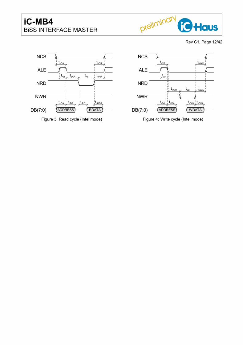
Figure 3: Read cycle (Intel mode) Figure 4: Write cycle (Intel mode)
preliminary
preliminary iC-MB4BiSS INTERFACE MASTER
Rev C1, Page 13/42
OPERATING REQUIREMENTS: µC Interface, MOTOROLA mode
Operating conditions: CFGSPI = 0, INT_NMOT = 0 VDD = 3.0 . . . 5.5 V, Tj = -40 . . . 125 °C;lo input level = 0 . . . 0.8 V, hi input level = 2.0 V . . . VDD, lo output level = 0 . . . 0.4 V, hi output level = 2.4 V . . . VDDAlias: RNW = NRD_RNW, E = NWR_EItem Symbol Parameter Conditions UnitNo. Min. Max.
I101 tsCA Setup Time:NCS lo before ALE hi→lo
10 ns
I102 tsDA Setup Time:Data stable before ALE hi→lo
15 ns
I103 thDA Hold Time:Data stable after ALE hi→lo
15 ns
I104 tAh Signal Duration:ALE at high level
10 ns
I105 tsAE Setup Time:ALE lo before E lo→hi
10 ns
I106 thAE Hold Time:ALE lo after E hi→lo
NCS = lo 10 ns
I107 tsRE Setup Time:RNW stable before E lo→hi
NCS = lo 10 ns
I108 thRE Hold Time:RNW stable after E hi→lo
NCS = lo 10 ns
I109 tEh Signal Duration:E at high level
NCS = lo 10 ns
I110 tpED1 Propagation Delay:Data stable after E lo→hi
NCS = lo,CL = 5 pF, VDD≥ 4.5 V, Tj = -40 . . . 85 °C 23 nsCL = 5 pF, VDD≥ 4.5 V 25 nsCL = 50 pF, VDD≥4.5 V, Tj = -40 . . . 85 °C 29 nsCL = 50 pF, VDD≥4.5 V 33 nsCL = 5 pF, Tj = -40 . . . 85 °C 38 nsCL = 5 pF 42 nsCL = 50 pF, Tj = -40 . . . 85 °C 49 nsCL = 50 pF 54 ns
I111 tpED2 Propagation Delay:Data bus high impedance after E hi→lo
NCS = lo, CL = 50 pF 25 ns
I112 tsDE Setup Time:Data stable before E hi→lo
NCS = lo 15 ns
I113 thDE Hold Time:Data stable after E hi→lo
NCS = lo 15 ns
I114 thCE Hold Time:NCS lo after E hi→lo
10 ns
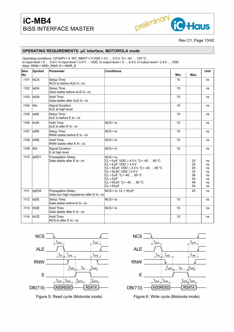
Figure 5: Read cycle (Motorola mode) Figure 6: Write cycle (Motorola mode)
preliminary
preliminary iC-MB4BiSS INTERFACE MASTER
Rev C1, Page 14/42
OPERATING REQUIREMENTS: µC Interface, SPI mode
Operating conditions: CFGSPI = 1 VDD = 3.0 . . . 5.5 V, Tj = -40 . . . 125 °C;lo input level = 0 . . . 0.8 V, hi input level = 2.0 V . . . VDD, lo output level = 0 . . . 0.4 V, hi output level = 2.4 V . . . VDDAlias: NCS = NCS/DB4, SCLK = ALE/DB5, MOSI = DB0/DB6, MISO = DB1/DB7Item Symbol Parameter Conditions UnitNo. Min. Max.
I201 tsCS Setup Time:NCS lo before SCLK lo→hi
10 ns
I202 thCS Hold Time:NCS lo after SCLK hi→lo
10 ns
I203 tSl Signal Duration:SCLK lo
10 ns
I204 tSh Signal Duration:SCLK hi
10 ns
during SPI command ’ReadData’ betweenaddress and data
100 ns
I205 tsDS Setup Time:MOSI stable before SCLK lo→hi
7.5 ns
I206 thDS Hold Time:MOSI stable after SCLK lo→hi
7.5 ns
I207 tpSD Propagation Delay:MISO stable after SCLK hi→lo
CL = 5 pF, VDD≥ 4.5 V, Tj = -40 . . . 85 °C 23 nsCL = 5 pF, VDD≥ 4.5 V 25 nsCL = 50 pF, VDD≥4.5 V, Tj = -40 . . . 85 °C 29 nsCL = 50 pF, VDD≥4.5 V 33 nsCL = 5 pF, Tj = -40 . . . 85 °C 38 nsCL = 5 pF 42 nsCL = 50 pF, Tj = -40 . . . 85 °C 49 nsCL = 50 pF 54 ns
I208 tpCD Propagation Delay:MISO high impedance after NCS lo→hi
CL = 50 pF 25 ns
I209 tCh Signal Duration:NCS hi
10 ns
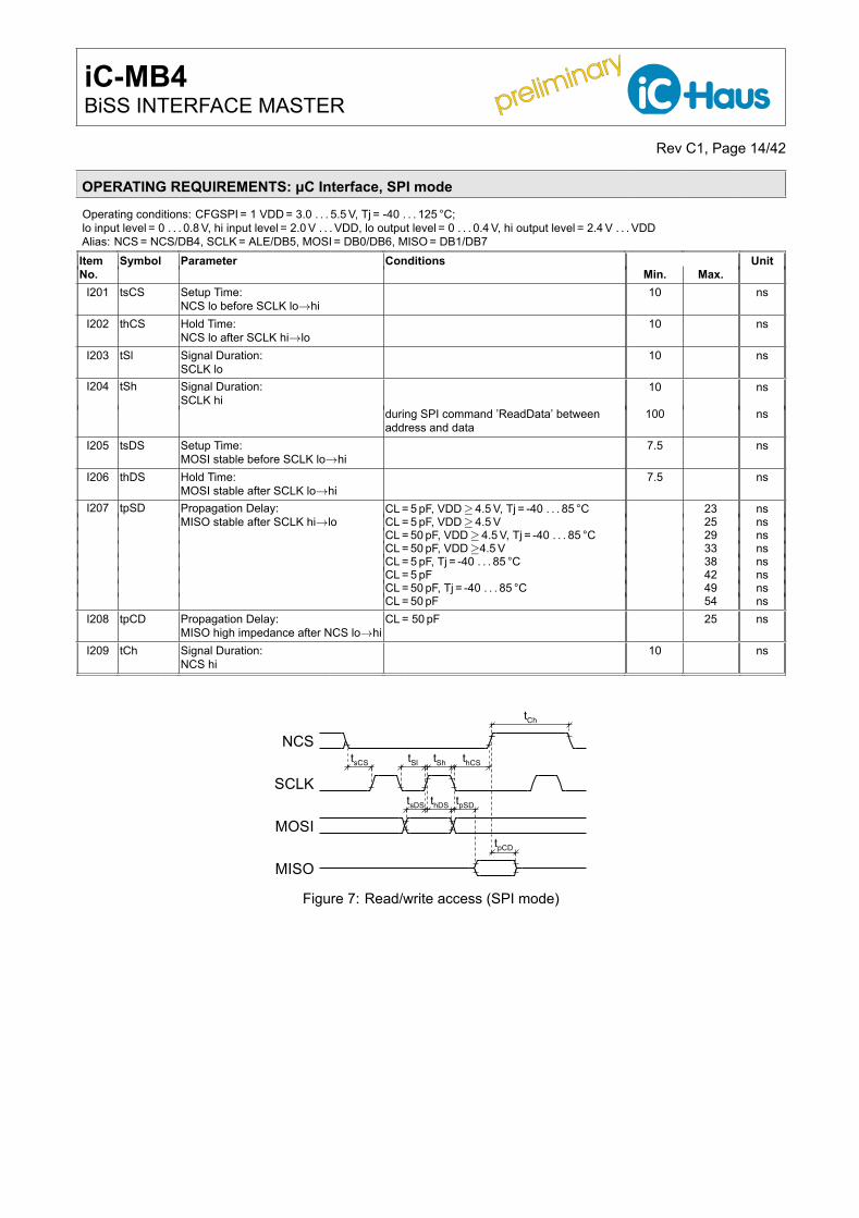
Figure 7: Read/write access (SPI mode)
preliminary
preliminary iC-MB4BiSS INTERFACE MASTER
Rev C1, Page 15/42
OPERATING REQUIREMENTS: BiSS Interface - BiSS B/C frame
Operating conditions: register bit SELSSI = 0 VDD = 3.0 . . . 5.5 V, Tj = -40 . . . 125 °CAlias: MA = MA1/MA2_NMA1, SL = SL1/SL2_NSL1Item Symbol Parameter Conditions UnitNo. Min. Max.Frame
I301 TMAS Clock Period FreqSens via FREQ(4:0) selected in 2 320 1/f(CLK)accordance with Table 41 on page 32
I302 tMASl Clock Signal Lo Level Duration 50 50 %TMAS
I303 tMASh Clock Signal Hi Level Duration 50 50 %TMAS
I304 tpLine Permissible Line Delay 0 indefiniteI305 ∆ tpL Permissible Propagation Delay of
Subsequent Clock Cycles vs. 1st ClockCycle
∆ tpL = max(|tpLine - tpLx|); x= 1 ... n 25 %TMAS
I306 Ttos Permissible Timeout (Slave) 55 %TMAS
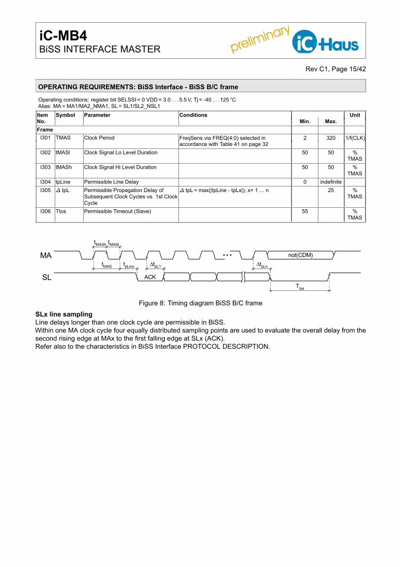
Figure 8: Timing diagram BiSS B/C frameSLx line samplingLine delays longer than one clock cycle are permissible in BiSS.Within one MA clock cycle four equally distributed sampling points are used to evaluate the overall delay from thesecond rising edge at MAx to the first falling edge at SLx (ACK).Refer also to the characteristics in BiSS Interface PROTOCOL DESCRIPTION.
preliminary
preliminary iC-MB4BiSS INTERFACE MASTER
Rev C1, Page 16/42
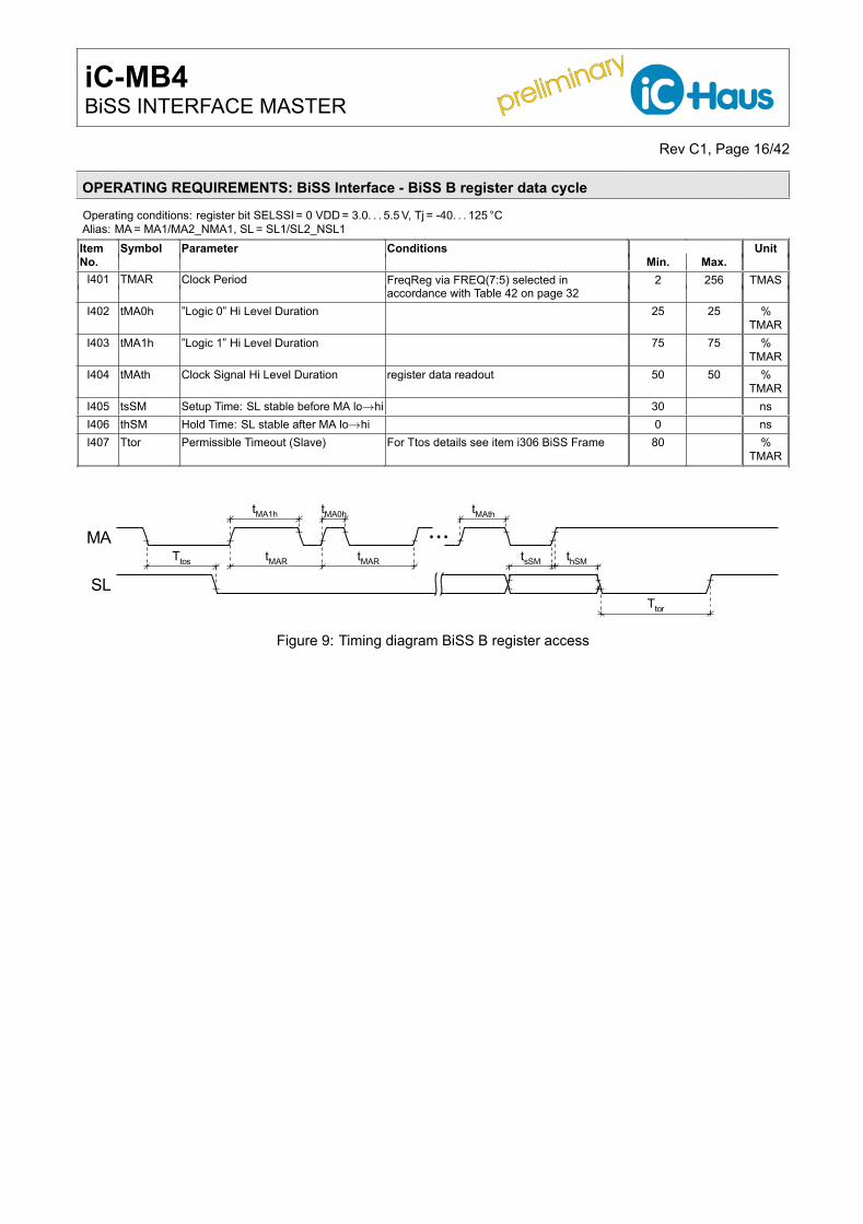
OPERATING REQUIREMENTS: BiSS Interface - BiSS B register data cycle
Operating conditions: register bit SELSSI = 0 VDD = 3.0. . . 5.5 V, Tj = -40. . . 125 °CAlias: MA = MA1/MA2_NMA1, SL = SL1/SL2_NSL1Item Symbol Parameter Conditions UnitNo. Min. Max.
I401 TMAR Clock Period FreqReg via FREQ(7:5) selected in 2 256 TMASaccordance with Table 42 on page 32
I402 tMA0h ”Logic 0” Hi Level Duration 25 25 %TMAR
I403 tMA1h ”Logic 1” Hi Level Duration 75 75 %TMAR
I404 tMAth Clock Signal Hi Level Duration register data readout 50 50 %TMAR
I405 tsSM Setup Time: SL stable before MA lo→hi 30 nsI406 thSM Hold Time: SL stable after MA lo→hi 0 nsI407 Ttor Permissible Timeout (Slave) For Ttos details see item i306 BiSS Frame 80 %
TMAR
Figure 9: Timing diagram BiSS B register access
preliminary
preliminary iC-MB4BiSS INTERFACE MASTER
Rev C1, Page 17/42
OPERATING REQUIREMENTS: BiSS Interface (SSI mode)
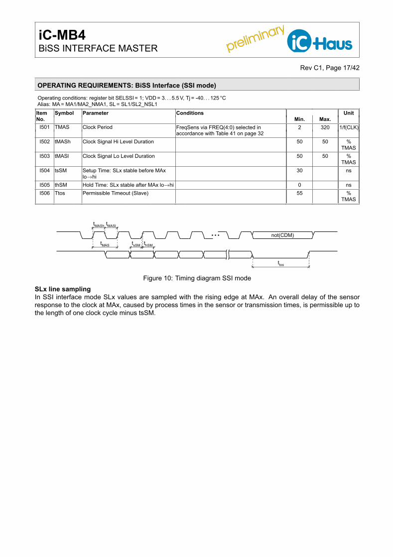
Operating conditions: register bit SELSSI = 1; VDD = 3. . . 5.5 V, Tj = -40. . . 125 °CAlias: MA = MA1/MA2_NMA1, SL = SL1/SL2_NSL1Item Symbol Parameter Conditions UnitNo. Min. Max.
I501 TMAS Clock Period FreqSens via FREQ(4:0) selected in 2 320 1/f(CLK)accordance with Table 41 on page 32
I502 tMASh Clock Signal Hi Level Duration 50 50 %TMAS
I503 tMASl Clock Signal Lo Level Duration 50 50 %TMAS
I504 tsSM Setup Time: SLx stable before MAxlo→hi
30 ns
I505 thSM Hold Time: SLx stable after MAx lo→hi 0 nsI506 Ttos Permissible Timeout (Slave) 55 %
TMAS
Figure 10: Timing diagram SSI modeSLx line samplingIn SSI interface mode SLx values are sampled with the rising edge at MAx. An overall delay of the sensorresponse to the clock at MAx, caused by process times in the sensor or transmission times, is permissible up tothe length of one clock cycle minus tsSM.
preliminary
preliminary iC-MB4BiSS INTERFACE MASTER
Rev C1, Page 18/42
CONFIGURATION PARAMETERS
Register Map . . . . . . . . . . . . . . . . . . . . . . . . . . . . . . Page 19
Sensor and Actuator Data . . . . . . . . . . . . . . . . Page 25SCDATAx: Single cycle data (SCD)
(sensor resp. actuator data, 64 bit perslave, 2 banks)
Register Data . . . . . . . . . . . . . . . . . . . . . . . . . . . . . Page 26RDATAx: Register data (64 byte)
Slave Configuration . . . . . . . . . . . . . . . . . . . . . . . Page 30SCDLENx: Single cycle data lengthENSCDx: Enable single cycle dataGRAYSx: Enable SCD gray to binary conversion
(SSI only)LSTOPx: Leading actuator stop bit control (BiSS
only)SELCRCSx: Selection between polynomial or
length for SCD CRC polynomialSCRCPOLYx: Polynomial for SCD CRC checkSCRCLENx: Polynomial selection by length for SCD
CRC checkSCRCSTARTx: Start value for polynomial SCD CRC
calculation
Control Communication . . . . . . . . . . . . . . . . . . Page 27REGADR: Register addressWNR: Read/write selectorREGNUM: Register countCHSEL: Channel selectorSLAVEID: Slave selectorREGVERS: BiSS model A/B or C selectorCTS: Register transmission or instruction se-
lectorIDS: Command/Instruction addressingCMD: Command/Instruction opcodeIDA_TEST: Verify ID-Acknowledge before executeHOLDCDM: Hold CDM (control data master)EN_MO: Enable output at MOx for actuator data
or delayed start bit
Master Configuration . . . . . . . . . . . . . . . . . . . . . Page 32FREQS: Frequency division Single Cycle DataFREQR: Frequency division register communi-
cation BiSS BFREQAGS: AutoGetSens Frequency divisionREVISION: RevisionVERSION: Device identifierSINGLEBANK: Use of only one RAM bank for SCDNOCRC: CRC for SCD not to be stored in RAMMO_BUSY: Configured processing delay of start
bit at output MOx
Channel Configuration . . . . . . . . . . . . . . . . . . . Page 34SLAVELOC5: Slave locationCFGCHx: Channel configuration
Slave Configuration 2 . . . . . . . . . . . . . . . . . . . . . Page 30ACTnSENS: Sensor or actuator data selector
Status Information . . . . . . . . . . . . . . . . . . . . . . . . Page 35EOT: Data transmission completednERR: Error at NER pinREGEND: Register data transmission completednREGERR: Error in control communicationnSCDERR: Error in single cycle data transmissionnDELAYERR: Missing start bit during register accessnAGSERR: Unable to start SCD frameSVALIDx: Single cycle data validREGBYTES: Number of valid register data transmit-
ted in case of errorCDSSEL: CDS of selected channelCDMTIME-OUT:
Control data timeout met
Instruction Register . . . . . . . . . . . . . . . . . . . . . . . Page 37INSTR: InstructionAGS: Automatic Get SensordataINIT: InitializeSWBANK: Switch RAM banksHOLDBANK: Inhibit RAM bank switchingBREAK: Data transmission interruptCLKENI: Enable internal clockENTEST: Enable factory test interfaceCFGIF: Configure physical interfacesMAFS: Master line control (selected channel)MAVS: Master line control (selected channel)MAFO: Master line control
(not selected channels)MAVO: Master line control
(not selected channels)
Status Information 2 . . . . . . . . . . . . . . . . . . . . . . Page 35SLx: Current SLx line levelCDSx: Control data bit slaveSWBANK-FAILS:
Bank switching for SCD failed
preliminary
preliminary iC-MB4BiSS INTERFACE MASTER
Rev C1, Page 19/42
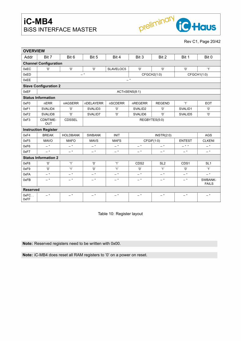
REGISTER MAP
OVERVIEWAddr Bit 7 Bit 6 Bit 5 Bit 4 Bit 3 Bit 2 Bit 1 Bit 0
Sensor and Actuator Data0x00 SCDATA1(7:0)0x01 . .0x07
SCDATA1(63:8)
0x08 . .0x3F
SCDATA2(63:0) . . SCDATA8(63:0)
0x40 . .0x7F
– ∗
Register Data0x80 † RDATA1(7:0)0x80 ‡ IDS(7:0)0x81 . .0xBF
RDATA2(7:0) . . RDATA64(7:0)
Configuration Slave 10xC0 GRAYS1 /
LSTOP1ENSCD1 SCDLEN1(5:0)
0xC1 SELCRCS1 SCRCLEN1(6:0) / SCRCPOLY1(7:1)0xC2 SCRCSTART1(7:0)0xC3 SCRCSTART1(15:8)0xC4 . .0xDF
Configuration Slave 2(31:0) . . Configuration Slave 8(31:0)
Control Communication Configuration0xE0 – ∗
0xE1 – ∗
0xE2 WNR REGADR(6:0)0xE3 – ∗ REGNUM(5:0)0xE4 – ∗ CHSEL(2:1)0xE5 † CTS REGVERS SLAVEID(2:0) – ∗ EN_MO HOLDCDM0xE5 ‡ CTS REGVERS CMD(1:0) IDA_TEST – ∗ EN_MO HOLDCDM
Master Configuration0xE6 FREQR(2:0) FREQS(4:0)0xE7 – ∗ NOCRC SINGLEBANK0xE8 FREQAGS(7:0)0xE9 MO_BUSY(7:0)0xEA REVISION(7:0)§
0xEB VERSION(7:0)§
∗ Reserved or unused register bits highlighted as ’–’ need to be written with 0 if a byte wide register write access is required.† Using register access in control communication.‡ Using command/instructions in control communication.§ Register bits with constant ’0’ or ’1’ are ROM-based values and can not be changed through writing.
preliminary
preliminary iC-MB4BiSS INTERFACE MASTER
Rev C1, Page 20/42
OVERVIEWAddr Bit 7 Bit 6 Bit 5 Bit 4 Bit 3 Bit 2 Bit 1 Bit 0
Channel Configuration0xEC ’0’ ’0’ ’0’ SLAVELOC5 ’0’ ’0’ ’0’ ’1’0xED – ∗ CFGCH2(1:0) CFGCH1(1:0)0xEE – ∗
Slave Configuration 20xEF ACTnSENS(8:1)
Status Information0xF0 nERR nAGSERR nDELAYERR nSCDERR nREGERR REGEND ’1’ EOT0xF1 SVALID4 ’0’ SVALID3 ’0’ SVALID2 ’0’ SVALID1 ’0’0xF2 SVALID8 ’0’ SVALID7 ’0’ SVALID6 ’0’ SVALID5 ’0’0xF3 CDMTIME-
OUTCDSSEL REGBYTES(5:0)
Instruction Register0xF4 BREAK HOLDBANK SWBANK INIT INSTR(2:0) AGS0xF5 MAVO MAFO MAVS MAFS CFGIF(1:0) ENTEST CLKENI0xF6 – ∗ – ∗ – ∗ – ∗ – ∗ – ∗ – ∗ ∗ – ∗
0xF7 – ∗ – ∗ – ∗ – ∗ – ∗ – ∗ – ∗ – ∗
Status Information 20xF8 ’0’ ’1’ ’0’ ’1’ CDS2 SL2 CDS1 SL10xF9 ’0’ ’1’ ’0’ ’1’ ’0’ ’1’ ’0’ ’1’0xFA – ∗ – ∗ – ∗ – ∗ – ∗ – ∗ – ∗ – ∗
0xFB – ∗ – ∗ – ∗ – ∗ – ∗ – ∗ – ∗ SWBANK-FAILS
Reserved0xFC . .0xFF
– ∗ – ∗ – ∗ – ∗ – ∗ – ∗ – ∗ – ∗
Table 10: Register layout
Note: Reserved registers need to be written with 0x00.
Note: iC-MB4 does reset all RAM registers to ’0’ on a power on reset.
preliminary
preliminary iC-MB4BiSS INTERFACE MASTER
Rev C1, Page 21/42
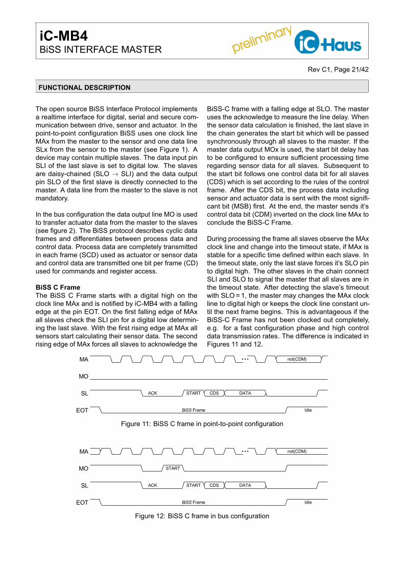
FUNCTIONAL DESCRIPTION
The open source BiSS Interface Protocol implementsa realtime interface for digital, serial and secure com-munication between drive, sensor and actuator. In thepoint-to-point configuration BiSS uses one clock lineMAx from the master to the sensor and one data lineSLx from the sensor to the master (see Figure 1). Adevice may contain multiple slaves. The data input pinSLI of the last slave is set to digital low. The slavesare daisy-chained (SLO → SLI) and the data outputpin SLO of the first slave is directly connected to themaster. A data line from the master to the slave is notmandatory.
In the bus configuration the data output line MO is usedto transfer actuator data from the master to the slaves(see figure 2). The BiSS protocol describes cyclic dataframes and differentiates between process data andcontrol data. Process data are completely transmittedin each frame (SCD) used as actuator or sensor dataand control data are transmitted one bit per frame (CD)used for commands and register access.
BiSS C FrameThe BiSS C Frame starts with a digital high on theclock line MAx and is notified by iC-MB4 with a fallingedge at the pin EOT. On the first falling edge of MAxall slaves check the SLI pin for a digital low determin-ing the last slave. With the first rising edge at MAx allsensors start calculating their sensor data. The secondrising edge of MAx forces all slaves to acknowledge the
BiSS-C frame with a falling edge at SLO. The masteruses the acknowledge to measure the line delay. Whenthe sensor data calculation is finished, the last slave inthe chain generates the start bit which will be passedsynchronously through all slaves to the master. If themaster data output MOx is used, the start bit delay hasto be configured to ensure sufficient processing timeregarding sensor data for all slaves. Subsequent tothe start bit follows one control data bit for all slaves(CDS) which is set according to the rules of the controlframe. After the CDS bit, the process data includingsensor and actuator data is sent with the most signifi-cant bit (MSB) first. At the end, the master sends it’scontrol data bit (CDM) inverted on the clock line MAx toconclude the BiSS-C Frame.
During processing the frame all slaves observe the MAxclock line and change into the timeout state, if MAx isstable for a specific time defined within each slave. Inthe timeout state, only the last slave forces it’s SLO pinto digital high. The other slaves in the chain connectSLI and SLO to signal the master that all slaves are inthe timeout state. After detecting the slave’s timeoutwith SLO = 1, the master may changes the MAx clockline to digital high or keeps the clock line constant un-til the next frame begins. This is advantageous if theBiSS-C Frame has not been clocked out completely,e.g. for a fast configuration phase and high controldata transmission rates. The difference is indicated inFigures 11 and 12.
Figure 11: BiSS C frame in point-to-point configuration
Figure 12: BiSS C frame in bus configuration
preliminary
preliminary iC-MB4BiSS INTERFACE MASTER
Rev C1, Page 22/42
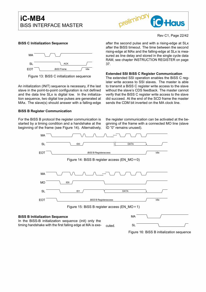
BiSS C Initialization Sequence
Figure 13: BiSS C initialization sequence
An initialization (INIT) sequence is necessary, if the lastslave in the point-to-point configuration is not definedand the data line SLx is digital low. In the initializa-tion sequence, two digital low pulses are generated atMAx. The slave(s) should answer with a falling-edge
after the second pulse and with a rising-edge at SLxafter the BiSS timeout. The time between the secondrising-edge at MAx and the falling-edge at SLx is mea-sured as line delay and stored in the single cycle dataRAM, see chapter INSTRUCTION REGISTER on page37.
Extended SSI BiSS C Register CommunicationThe extended SSI operation enables the BiSS C reg-ister write access to SSI slaves. The master is ableto transmit a BiSS C register write access to the slavewithout the slave’s CDS feedback. The master cannotverify that the BiSS C register write access to the slavedid succeed. At the end of the SCD frame the mastersends the CDM bit inverted on the MA clock line.
BiSS B Register Communication
For the BiSS B protocol the register communication isstarted by a timing condition and a handshake at thebeginning of the frame (see Figure 14). Alternatively,
the register communication can be activated at the be-ginning of the frame with a connected MO line (slaveID ”0” remains unused).
Figure 14: BiSS B register access (EN_MO = 0)
Figure 15: BiSS B register access (EN_MO = 1)
BiSS B Initialization SequenceIn the BiSS-B initialization sequence (init) only thetiming handshake with the first falling edge at MA is exe- cuted.
Figure 16: BiSS B initialization sequence
preliminary
preliminary iC-MB4BiSS INTERFACE MASTER
Rev C1, Page 23/42
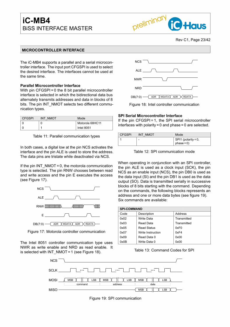
MICROCONTROLLER INTERFACE
The iC-MB4 supports a parallel and a serial microcon-troller interface. The input port CFGSPI is used to selectthe desired interface. The interfaces cannot be used atthe same time.
Parallel Microcontroller InterfaceWith pin CFGSPI = 0 the 8 bit parallel microcontrollerinterface is selected in which the bidirectional data busalternately transmits addresses and data in blocks of 8bits. The pin INT_NMOT selects two different commu-nication types.
CFGSPI INT_NMOT Mode0 0 Motorola 68HC110 1 Intel 8051
Table 11: Parallel communication types
In both cases, a digital low at the pin NCS activates theinterface and the pin ALE is used to store the address.The data pins are tristate while deactivated via NCS.
If the pin INT_NMOT = 0, the motorola communicationtype is selected. The pin RNW chooses between readand write access and the pin E executes the access(see Figure 17).
Figure 17: Motorola controller communication
The Intel 8051 controller communication type usesNWR as write enable and NRD as read enable. Itis selected with INT_NMOT = 1 (see Figure 18).
Figure 18: Intel controller communication
SPI Serial Microcontroller InterfaceIf the pin CFGSPI = 1, the SPI serial microcontrollerinterfaces with polarity = 0 and phase = 0 are selected.
CFGSPI INT_NMOT Mode1 - SPI1 (polarity = 0,
phase = 0)
Table 12: SPI communication mode
When operating in conjunction with an SPI controller,the pin ALE is used as a clock input (SCK), the pinNCS as an enable input (NCS), the pin DB0 is used asthe data input (SI) and the pin DB1 is used as the dataoutput (SO). Data is transmitted serially in successiveblocks of 8 bits starting with the command. Dependingon the commands, the following blocks represents anaddress and one or more data bytes (see figure 19).Six commands are available:
SPI-COMMANDCode Description Address0x02 Write Data Transmitted0x03 Read Data Transmitted0x05 Read Status 0xF00x07 Write Instruction 0xF40x09 Read Data 0 0x000x0B Write Data 0 0x00
Table 13: Command Codes for SPI
Figure 19: SPI communication
preliminary
preliminary iC-MB4BiSS INTERFACE MASTER
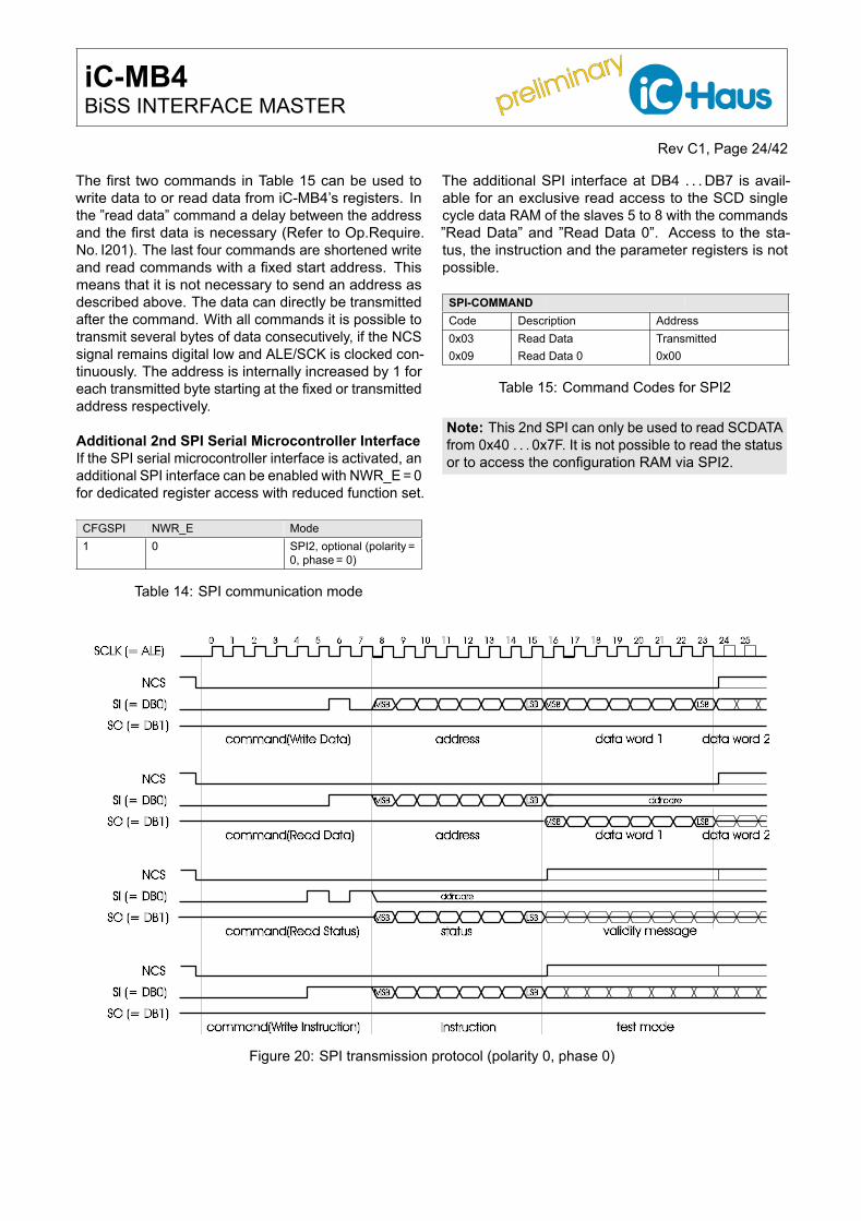
Rev C1, Page 24/42
The first two commands in Table 15 can be used towrite data to or read data from iC-MB4’s registers. Inthe ”read data” command a delay between the addressand the first data is necessary (Refer to Op.Require.No. I201). The last four commands are shortened writeand read commands with a fixed start address. Thismeans that it is not necessary to send an address asdescribed above. The data can directly be transmittedafter the command. With all commands it is possible totransmit several bytes of data consecutively, if the NCSsignal remains digital low and ALE/SCK is clocked con-tinuously. The address is internally increased by 1 foreach transmitted byte starting at the fixed or transmittedaddress respectively.
Additional 2nd SPI Serial Microcontroller InterfaceIf the SPI serial microcontroller interface is activated, anadditional SPI interface can be enabled with NWR_E = 0for dedicated register access with reduced function set.
CFGSPI NWR_E Mode1 0 SPI2, optional (polarity =
0, phase = 0)
Table 14: SPI communication mode
The additional SPI interface at DB4 . . . DB7 is avail-able for an exclusive read access to the SCD singlecycle data RAM of the slaves 5 to 8 with the commands”Read Data” and ”Read Data 0”. Access to the sta-tus, the instruction and the parameter registers is notpossible.
SPI-COMMANDCode Description Address0x03 Read Data Transmitted0x09 Read Data 0 0x00
Table 15: Command Codes for SPI2
Note: This 2nd SPI can only be used to read SCDATAfrom 0x40 . . . 0x7F. It is not possible to read the statusor to access the configuration RAM via SPI2.
Figure 20: SPI transmission protocol (polarity 0, phase 0)
preliminary
preliminary iC-MB4BiSS INTERFACE MASTER
Rev C1, Page 25/42
SENSOR AND ACTUATOR DATA
The process data memory buffers the sensor and actu-ator data and has eight bytes of memory for each slave.Eight slaves are supported. The address mapping isshown in Table 16.
SCDATA Addr. 0x00 . . . 0x3F; bit 7:0 R/WAddr. Content0x00 SCDATA1(7:0)0x01 SCDATA1(15:8)0x02 SCDATA1(23:16)0x03 SCDATA1(31:24)0x04 SCDATA1(39:32)0x05 SCDATA1(47:40)0x06 SCDATA1(55:48)0x07 SCDATA1(63:56)0x08 . .0x0F
SCDATA2(63:0)
0x10 . .0x17
SCDATA3(63:0)
0x18 . .0x1F
SCDATA4(63:0)
0x20 . .0x27
SCDATA5(63:0)
0x28 . .0x2F
SCDATA6(63:0)
0x30 . .0x37
SCDATA7(63:0)
0x38 . .0x3F
SCDATA8(63:0)
Table 16: Address mapping of sensor data
The sensor data is arranged in the memory area withthe least significant bit (LSB) at the lowermost addressat bit position 0. The memory is written byte-by-byteand unused bits are set to zero. Unused bytes remainunchanged. If there is sufficient free memory avail-able for CRC data, the read and inverted CRC bits arestored beginning at the highest address downwards.The storage of the CRC can be disabled with NOCRC(see Table 44).
Example: BiSS Sensor Bus with 3 SlavesThe following example shows the address mappingof the sensor data and CRC bits generated by threeslaves.
Slave 1: 19+2 bits of sensor data, 6 bits of CRC=> total length of 27 bits
Slave 2: 12+2 bits of sensor data, 5 bits of CRC=> total length of 19 bits
Slave 3: 24 bits of sensor data, 16 bits of CRC=> total length of 40 bits
SCDATA Addr. 0x00 . . . 0x3FAddr. bit 7 bit 6 bit 5 bit 4 bit 3 bit 2 bit 1 bit 00x00 Sensor data 1(7:0)0x01 Sensor data 1(15:8)0x02 0 0 0 Sensor data 1(20:16)0x03 . . not changed0x060x07 0 0 CRC 1(5:0)0x08 Sensor data 2(7:0)0x09 0 0 Sensor data 2(13:8)0x0A . . not changed0x0E0x0F 0 0 0 CRC 2(4:0)0x10 Sensor data 3(7:0)0x11 Sensor data 3(15:8)0x12 Sensor data 3(23:16)0x13 . . not changed0x150x16 CRC 3(7:0)0x17 CRC 3(15:8)0x18 . . not changed0x3F
Table 17: Example address mapping of sensor data
In order to import new sensor data during controller ac-cesses, iC-MB4 has two memory banks for sensor data.While sensor data is being read and written into the firstRAM bank during processing of the BiSS Frame, thesecond RAM bank section containing sensor data ofthe previous frame can be read by the controller. Therelevant sensor data memory banks are swapped atthe end of the BiSS Frame. This can be prevented bythe controller entering the command register bit HOLD-BANK (see Table 72). Simultaneously the validity regis-ter (SVALIDx, Table 61) is also swapped.
preliminary
preliminary iC-MB4BiSS INTERFACE MASTER
Rev C1, Page 26/42
REGISTER DATA
The iC-MB4 has an individual storage area used forthe data of the automatic register communication. Incase of a write access to the slaves the storage areamust be written with the register data before startingthe communication. The same memory area is alsoused for the read data coming from the slave duringread access. The memory size of the storage area is64 bytes.
RDATA Addr. 0x80 . . . 0xBF; bit 7:0 R/WAddr. Content0x80 RDATA1(7:0)0x81 . .0xBF
RDATA2(7:0) . . . RDATA64(7:0)
Table 18: RDATA address range for register communi-cation
The slave addressing IDS which is used in commandsmust be stored at address 0x80.
IDS Addr. 0x80; bit 7:0 R/WAddr. Content0x80 IDS(7:0)
Table 19: IDS for commands
preliminary
preliminary iC-MB4BiSS INTERFACE MASTER
Rev C1, Page 27/42
CONTROL COMMUNICATION
The control frame enables protected and confirmedreading and writing of the registers of a slave. It is alsoused for protected and confirmed sending of commandsto specified slaves or to all slaves. The control frame iscompounded of 1 bit per BiSS C frame in each direc-tion. The control bit sent from the master to the slavesis called CDM and control bit sent from the slaves to themaster is called CDS. For more information about thecontrol communication refer to the BiSS Interface PRO-TOCOL DESCRIPTION.
The iC-MB4 does support autonomous register commu-nication with BiSS B and BiSS C. REGVERS is usedto select the protocol type. For register write accesswith extended SSI the BiSS C protocol type needs tobe selected.
REGVERS Addr. 0xE5; bit 6 R/WCode Function0 Register communication BiSS A/B1 Register communication BiSS C
Table 20: Type of protocol for register access
If more than one physical BiSS channel is used, theone-hot coded parameter CHSEL selects the channelthat is used for control communication. For commandsit is possible to run the control communication on sev-eral channels simultaneously.
CHSEL(1) Addr. 0xE4; bit 0 R/WCode Function0 Channel 1 not used ∗
1 Channel 1 used for control communicationCHSEL(2) Addr. 0xE4; bit 1 R/W0 Channel 2 not used1 Channel 2 used for control communication †
Table 21: Channel mapping for control communication
The selection between commands and register accessis done with the parameter CTS.
CTS Addr. 0xE5; bit 7 R/WCode Function0 Command/instruction communication1 Register accessNote The parameter CTS was called MSEL in former
MB100 or iC-MB3 data sheets.
Table 22: Type of control communication
The parameter HOLDCDM determines the behaviour ofthe pin MA at the end of the frame. If the pin SL is notdigital low at the end of the frame, because the BiSS Cframe has not been clocked out completely, the pin MAmust be programmed with HOLDCDM to be constantuntil the next frame begins.
HOLDCDM Addr. 0xE5; bit 0 R/WCode Function0 MA changes to digital after detecting the slave’s
timeout1 MA remains constant until the next frame begins
Table 23: Behaviour of the pin MA at the end of frame
∗ Channel 1 is selected if CHSEL(2:1)=0.† Channel 2 is not available with iC-MB4 TSSOP24.
preliminary
preliminary iC-MB4BiSS INTERFACE MASTER
Rev C1, Page 28/42
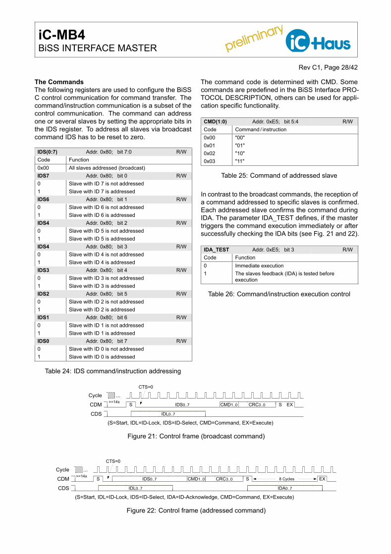
The CommandsThe following registers are used to configure the BiSSC control communication for command transfer. Thecommand/instruction communication is a subset of thecontrol communication. The command can addressone or several slaves by setting the appropriate bits inthe IDS register. To address all slaves via broadcastcommand IDS has to be reset to zero.
IDS(0:7) Addr. 0x80; bit 7:0 R/WCode Function0x00 All slaves addressed (broadcast)IDS7 Addr. 0x80; bit 0 R/W0 Slave with ID 7 is not addressed1 Slave with ID 7 is addressedIDS6 Addr. 0x80; bit 1 R/W0 Slave with ID 6 is not addressed1 Slave with ID 6 is addressedIDS4 Addr. 0x80; bit 2 R/W0 Slave with ID 5 is not addressed1 Slave with ID 5 is addressedIDS4 Addr. 0x80; bit 3 R/W0 Slave with ID 4 is not addressed1 Slave with ID 4 is addressedIDS3 Addr. 0x80; bit 4 R/W0 Slave with ID 3 is not addressed1 Slave with ID 3 is addressedIDS2 Addr. 0x80; bit 5 R/W0 Slave with ID 2 is not addressed1 Slave with ID 2 is addressedIDS1 Addr. 0x80; bit 6 R/W0 Slave with ID 1 is not addressed1 Slave with ID 1 is addressedIDS0 Addr. 0x80; bit 7 R/W0 Slave with ID 0 is not addressed1 Slave with ID 0 is addressed
Table 24: IDS command/instruction addressing
The command code is determined with CMD. Somecommands are predefined in the BiSS Interface PRO-TOCOL DESCRIPTION, others can be used for appli-cation specific functionality.
CMD(1:0) Addr. 0xE5; bit 5:4 R/WCode Command / instruction0x00 "00"0x01 "01"0x02 "10"0x03 "11"
Table 25: Command of addressed slave
In contrast to the broadcast commands, the reception ofa command addressed to specific slaves is confirmed.Each addressed slave confirms the command duringIDA. The parameter IDA_TEST defines, if the mastertriggers the command execution immediately or aftersuccessfully checking the IDA bits (see Fig. 21 and 22).
IDA_TEST Addr. 0xE5; bit 3 R/WCode Function0 Immediate execution1 The slaves feedback (IDA) is tested before
execution
Table 26: Command/instruction execution control
Figure 21: Control frame (broadcast command)
Figure 22: Control frame (addressed command)
preliminary
preliminary iC-MB4BiSS INTERFACE MASTER
Rev C1, Page 29/42
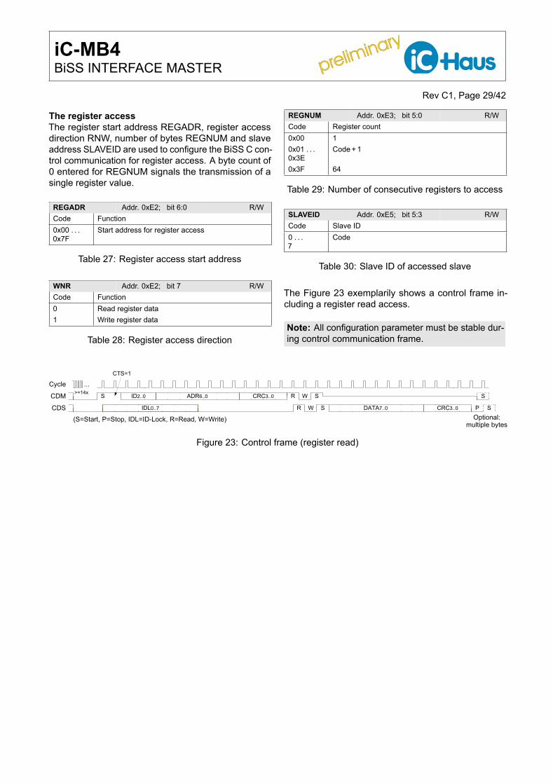
The register accessThe register start address REGADR, register accessdirection RNW, number of bytes REGNUM and slaveaddress SLAVEID are used to configure the BiSS C con-trol communication for register access. A byte count of0 entered for REGNUM signals the transmission of asingle register value.
REGADR Addr. 0xE2; bit 6:0 R/WCode Function0x00 . . .0x7F
Start address for register access
Table 27: Register access start address
WNR Addr. 0xE2; bit 7 R/WCode Function0 Read register data1 Write register data
Table 28: Register access direction
REGNUM Addr. 0xE3; bit 5:0 R/WCode Register count0x00 10x01 . . .0x3E
Code + 1
0x3F 64
Table 29: Number of consecutive registers to access
SLAVEID Addr. 0xE5; bit 5:3 R/WCode Slave ID0 . . .7
Code
Table 30: Slave ID of accessed slave
The Figure 23 exemplarily shows a control frame in-cluding a register read access.
Note: All configuration parameter must be stable dur-ing control communication frame.
Figure 23: Control frame (register read)
preliminary
preliminary iC-MB4BiSS INTERFACE MASTER
Rev C1, Page 30/42
SLAVE CONFIGURATION
The process data consists of a maximum of eight logi-cal data channels. The slave configuration determinesthe setup of each data channel. The iC-MB4 provides aprogrammable data length, CRC polynomial and CRCstart value for each logical data slave.
ENSCD1 Addr. 0xC0; bit 6 R/WENSCD2 Addr. 0xC4; bit 6 R/WENSCD3 Addr. 0xC8; bit 6 R/WENSCD4 Addr. 0xCC; bit 6 R/WENSCD5 Addr. 0xD0; bit 6 R/WENSCD6 Addr. 0xD4; bit 6 R/WENSCD7 Addr. 0xD8; bit 6 R/WENSCD8 Addr. 0xDC; bit 6 R/WCode Function0 Single cycle data not available1 Single cycle data available
Table 31: Enable single cycle data for slave x
SCDLEN1 Addr. 0xC0; bit 5:0 R/WSCDLEN2 Addr. 0xC4; bit 5:0 R/WSCDLEN3 Addr. 0xC8; bit 5:0 R/WSCDLEN4 Addr. 0xCC; bit 5:0 R/WSCDLEN5 Addr. 0xD0; bit 5:0 R/WSCDLEN6 Addr. 0xD4; bit 5:0 R/WSCDLEN7 Addr. 0xD8; bit 5:0 R/WSCDLEN8 Addr. 0xDC; bit 5:0 R/WCode Single cycle data length0 1. . . Code + 163 64
Table 32: Single cycle data length of slave x
SELCRCS1 Addr. 0xC1; bit 7 R/WSELCRCS2 Addr. 0xC5; bit 7 R/WSELCRCS3 Addr. 0xC9; bit 7 R/WSELCRCS4 Addr. 0xCD; bit 7 R/WSELCRCS5 Addr. 0xD1; bit 7 R/WSELCRCS6 Addr. 0xD5; bit 7 R/WSELCRCS7 Addr. 0xD9; bit 7 R/WSELCRCS8 Addr. 0xDD; bit 7 R/WCode Function0 CRC bit length in SCRCLENx apply predefined CRC
polynomials1 CRC polynomial(7:1) in SCRCPOLYx
Table 33: CRC polynomial selection
BiSS uses CRC polynomials depending on the datalength predefined in the EDS and Profile Definitions.The parameter SELCRCS chooses between predefined
polynomials selected according to the CRC length andnon predefined polynomials for CRCs with a length ofup to seven bits. If CRCLEN = 0, the CRC verificationis deactivated.
SCRCLEN1 Addr. 0xC1; bit 6:0 R/WSCRCLEN2 Addr. 0xC5; bit 6:0 R/WSCRCLEN3 Addr. 0xC9; bit 6:0 R/WSCRCLEN4 Addr. 0xCD; bit 6:0 R/WSCRCLEN5 Addr. 0xD1; bit 6:0 R/WSCRCLEN6 Addr. 0xD5; bit 6:0 R/WSCRCLEN7 Addr. 0xD9; bit 6:0 R/WSCRCLEN8 Addr. 0xDD; bit 6:0 R/WCode CRC polynomial for single cycle data0 CRC verification deactivated3 0b1011 = 0xB4 0b1.0011 = 0x135 0b10.0101 = 0x256 0b100.0011 = 0x437 0b1000.1001 = 0x898 0b1.0010.1111 = 0x12F16 0b1.1001.0000.1101.1001 = 0x190D9. . . Other codes are not permitted.
Table 34: CRC length with predefined CRC polynomial
Since the least significant bit of the CRC polynomialis always 1, there is no need to store this informationin the CRC polynomial register. Therefore a maximumpolynomial length of 8 bit is possible. If the maximum8 bit polynomial length is not required, the used poly-nomial (without the LSB bit) is stored right aligned andleading bits are filled with 0.Example: The CRC polynomial 0x43 = 100 0011b isstored as 010 0001b (register value 0x21).
SCRCPOLY1 Addr. 0xC1; bit 6:0 R/WSCRCPOLY2 Addr. 0xC5; bit 6:0 R/WSCRCPOLY3 Addr. 0xC9; bit 6:0 R/WSCRCPOLY4 Addr. 0xCD; bit 6:0 R/WSCRCPOLY5 Addr. 0xD1; bit 6:0 R/WSCRCPOLY6 Addr. 0xD5; bit 6:0 R/WSCRCPOLY7 Addr. 0xD9; bit 6:0 R/WSCRCPOLY8 Addr. 0xDD; bit 6:0 R/WCode CRC polynomial for single cycle data0x00 CRC verification deactivated0x01 . .0x7F
Code & ’1’
Table 35: CRC polynomial
The CRC start values can be used to safely differenti-ate between SCD data words e.g. two position words
preliminary
preliminary iC-MB4BiSS INTERFACE MASTER
Rev C1, Page 31/42
provided by two different sensors. The same CRC startvalue that is used in the sensor needs to be applied inthe master to validate the received single cycle data.The CRC start value has a length of 16 bit and is dividedinto two consecutive 8-bit registers. A typical defaultslave CRC start value is 0x0000.
SCRCSTART1_L Addr. 0xC2; bit 7:0 R/WSCRCSTART1_H Addr. 0xC3; bit 7:0 R/WSCRCSTART2_L Addr. 0xC6; bit 7:0 R/WSCRCSTART2_H Addr. 0xC7; bit 7:0 R/WSCRCSTART3_L Addr. 0xCA; bit 7:0 R/WSCRCSTART3_H Addr. 0xCB; bit 7:0 R/WSCRCSTART4_L Addr. 0xCE; bit 7:0 R/WSCRCSTART4_H Addr. 0xCF; bit 7:0 R/WSCRCSTART5_L Addr. 0xD2; bit 7:0 R/WSCRCSTART5_H Addr. 0xD3; bit 7:0 R/WSCRCSTART6_L Addr. 0xD6; bit 7:0 R/WSCRCSTART6_H Addr. 0xD7; bit 7:0 R/WSCRCSTART7_L Addr. 0xDA; bit 7:0 R/WSCRCSTART7_H Addr. 0xDB; bit 7:0 R/WSCRCSTART8_L Addr. 0xDE; bit 7:0 R/WSCRCSTART8_H Addr. 0xDF; bit 7:0 R/WCode CRC start value for single cycle data0x0000 . .0xFFFF
SCRSTARTx_HI & CRCSTARTx_LO
Table 36: CRC calculation start value
Each data channel can be enabled to contain actuatordata or sensor data. The ACTnSENS parameter de-fines the functionality of each BiSS slave on the BiSSbus.
ACTnSENS1 Addr. 0xEF; bit 0 R/WACTnSENS2 Addr. 0xEF; bit 1 R/WACTnSENS3 Addr. 0xEF; bit 2 R/WACTnSENS4 Addr. 0xEF; bit 3 R/WACTnSENS5 Addr. 0xEF; bit 4 R/WACTnSENS6 Addr. 0xEF; bit 5 R/WACTnSENS7 Addr. 0xEF; bit 6 R/WACTnSENS8 Addr. 0xEF; bit 7 R/WCode Function0 Slave is configured as sensor1 Slave is configured as actuator
Table 37: Slave functionality control
Typically, a BiSS slave expects a leading stop bit beforethe actuator data which must be enabled with LSTOP(refer to BiSS Interface PROTOCOL DESCRIPTION).
LSTOP1 Addr. 0xC0; bit 7 R/WLSTOP2 Addr. 0xC4; bit 7 R/WLSTOP3 Addr. 0xC8; bit 7 R/WLSTOP4 Addr. 0xCC; bit 7 R/WLSTOP5 Addr. 0xD0; bit 7 R/WLSTOP6 Addr. 0xD4; bit 7 R/WLSTOP7 Addr. 0xD8; bit 7 R/WLSTOP8 Addr. 0xDC; bit 7 R/WCode Function0 No leading STOP bit on single cycle actuator data1 Leading STOP bit on single cycle actuator data
Table 38: Actuator stop bit control
The parameter GRAY activates a GRAY to binary con-version for SSI encoder.
GRAYS1 Addr. 0xC0; bit 7 R/WGRAYS2 Addr. 0xC4; bit 7 R/WGRAYS3 Addr. 0xC8; bit 7 R/WGRAYS4 Addr. 0xCC; bit 7 R/WGRAYS5 Addr. 0xD0; bit 7 R/WGRAYS6 Addr. 0xD4; bit 7 R/WGRAYS7 Addr. 0xD8; bit 7 R/WGRAYS8 Addr. 0xDC; bit 7 R/WCode Function0 SSI single cycle data binary coded1 SSI single cycle data GRAY coded
Table 39: SSI format is GRAY code
preliminary
preliminary iC-MB4BiSS INTERFACE MASTER
Rev C1, Page 32/42
MASTER CONFIGURATION
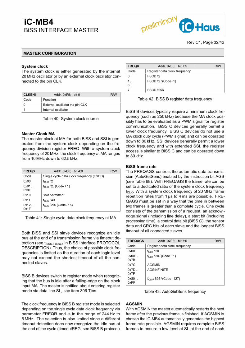
System clockThe system clock is either generated by the internal20 MHz oscillator or by an external clock oscillator con-nected to the pin CLK.
CLKENI Addr. 0xF5; bit 0 R/WCode Function0 External oscillator via pin CLK1 Internal oscillator
Table 40: System clock source
Master Clock MAThe master clock at MA for both BiSS and SSI is gen-erated from the system clock depending on the fre-quency division register FREQ. With a system clockfrequency of 20 MHz, the clock frequency at MA rangesfrom 10 MHz down to 62.5 kHz.
FREQS Addr. 0xE6; bit 4:0 R/WCode Single cycle data clock frequency (FSCD)0x00 fCLK / 20x01 . .0x0F
fCLK / 2 / (Code + 1)
0x10 ”not permitted”0x11 fCLK / 400x12 . .0x1F
fCLK / 20 / (Code - 15)
Table 41: Single cycle data clock frequency at MA
Both BiSS and SSI slave devices recognize an idlebus at the end of a transmission frame via timeout de-tection (see tBiSS-Timeout in BiSS Interface PROTOCOLDESCRIPTION). Thus, the choice of possible clock fre-quencies is limited as the duration of each logic levelmay not exceed the shortest timeout of all the con-nected slaves.
BiSS B devices switch to register mode when recogniz-ing that the bus is idle after a falling-edge on the clockinput MA. The master is notified about entering registermode via data line SL, see item 306 Ttos.
The clock frequency in BiSS B register mode is selecteddepending on the single cycle data clock frequency viaparameter FREQR and is in the range of 244 Hz to5 MHz. The selection is also limited since a differenttimeout detection does now recognize the idle bus atthe end of the cycle (timeoutREG, see BiSS B protocol).
FREQR Addr. 0xE6; bit 7:5 R/WCode Register data clock frequency0 FSCD / 21 . .6
FSCD / 2 / (Code+1)
7 FSCD / 256
Table 42: BiSS B register data frequency
BiSS B devices typically require a minimum clock fre-quency (such as 250 kHz) because the MA clock pos-sibly has to be evaluated as a PWM signal for registercommunication. BiSS C devices generally permit alower clock frequency. BiSS C devices do not use aMA clock duty cycle (PWM signal) and can be operateddown to 80 kHz. SSI devices generally permit a lowerclock frequency and with extended SSI, the registeraccess is similar to BiSS C and can be operated downto 80 kHz.
BiSS frame rateThe FREQAGS controls the automatic data transmis-sion (AutoGetSens) enabled by the instruction bit AGS(see Table 68). With FREQAGS the frame rate can beset to a dedicated ratio of the system clock frequencyfCLK. With a system clock frequency of 20 MHz framerepetition rates from 1µs to 4 ms are possible. FRE-QAGS must be set in a way that the time in betweentwo frames is greater than a complete cycle. One cycleconsists of the transmission of a request, an acknowl-edge signal (including line delay), a start bit (includingprocessing time), a control data bit (BiSS C), the sensordata and CRC bits of each slave and the longest BiSStimeout of all connected slaves.
FREQAGS Addr. 0xE8; bit 7:0 R/WCode Register data clock frequency0x00 fCLK / 200x00 . .0x7B
fCLK / 20 / (Code +1)
0x7C AGSMIN0x7D . .0x7F
AGSINFINITE
0x80 . .0xFF
fCLK/ 625 / (Code - 127)
Table 43: AutoGetSens frequency
AGSMINWith AGSMIN the master automatically restarts the nextframe after the previous frame is finished. If AGSMIN ischosen the iC-MB4 automatically generates the highestframe rate possible. AGSMIN requires complete BiSSframes to ensure a low level at SL at the end of each
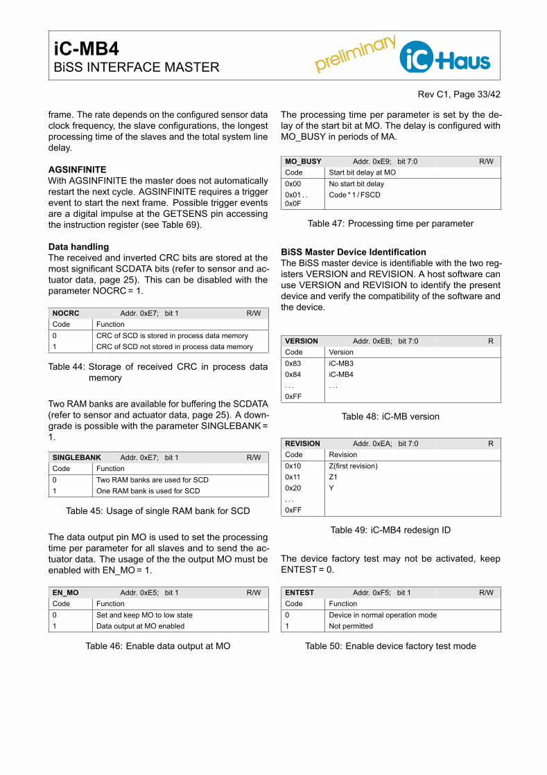
preliminary
preliminary iC-MB4BiSS INTERFACE MASTER
Rev C1, Page 33/42
frame. The rate depends on the configured sensor dataclock frequency, the slave configurations, the longestprocessing time of the slaves and the total system linedelay.
AGSINFINITEWith AGSINFINITE the master does not automaticallyrestart the next cycle. AGSINFINITE requires a triggerevent to start the next frame. Possible trigger eventsare a digital impulse at the GETSENS pin accessingthe instruction register (see Table 69).
Data handlingThe received and inverted CRC bits are stored at themost significant SCDATA bits (refer to sensor and ac-tuator data, page 25). This can be disabled with theparameter NOCRC = 1.
NOCRC Addr. 0xE7; bit 1 R/WCode Function0 CRC of SCD is stored in process data memory1 CRC of SCD not stored in process data memory
Table 44: Storage of received CRC in process datamemory
Two RAM banks are available for buffering the SCDATA(refer to sensor and actuator data, page 25). A down-grade is possible with the parameter SINGLEBANK =1.
SINGLEBANK Addr. 0xE7; bit 1 R/WCode Function0 Two RAM banks are used for SCD1 One RAM bank is used for SCD
Table 45: Usage of single RAM bank for SCD
The data output pin MO is used to set the processingtime per parameter for all slaves and to send the ac-tuator data. The usage of the the output MO must beenabled with EN_MO = 1.
EN_MO Addr. 0xE5; bit 1 R/WCode Function0 Set and keep MO to low state1 Data output at MO enabled
Table 46: Enable data output at MO
The processing time per parameter is set by the de-lay of the start bit at MO. The delay is configured withMO_BUSY in periods of MA.
MO_BUSY Addr. 0xE9; bit 7:0 R/WCode Start bit delay at MO0x00 No start bit delay0x01 . .0x0F
Code * 1 / FSCD
Table 47: Processing time per parameter
BiSS Master Device IdentificationThe BiSS master device is identifiable with the two reg-isters VERSION and REVISION. A host software canuse VERSION and REVISION to identify the presentdevice and verify the compatibility of the software andthe device.
VERSION Addr. 0xEB; bit 7:0 RCode Version0x83 iC-MB30x84 iC-MB4. . . . . .0xFF
Table 48: iC-MB version
REVISION Addr. 0xEA; bit 7:0 RCode Revision0x10 Z(first revision)0x11 Z10x20 Y. . .0xFF
Table 49: iC-MB4 redesign ID
The device factory test may not be activated, keepENTEST = 0.
ENTEST Addr. 0xF5; bit 1 R/WCode Function0 Device in normal operation mode1 Not permitted
Table 50: Enable device factory test mode
preliminary
preliminary iC-MB4BiSS INTERFACE MASTER
Rev C1, Page 34/42
CONFIGURATION CHANNELS
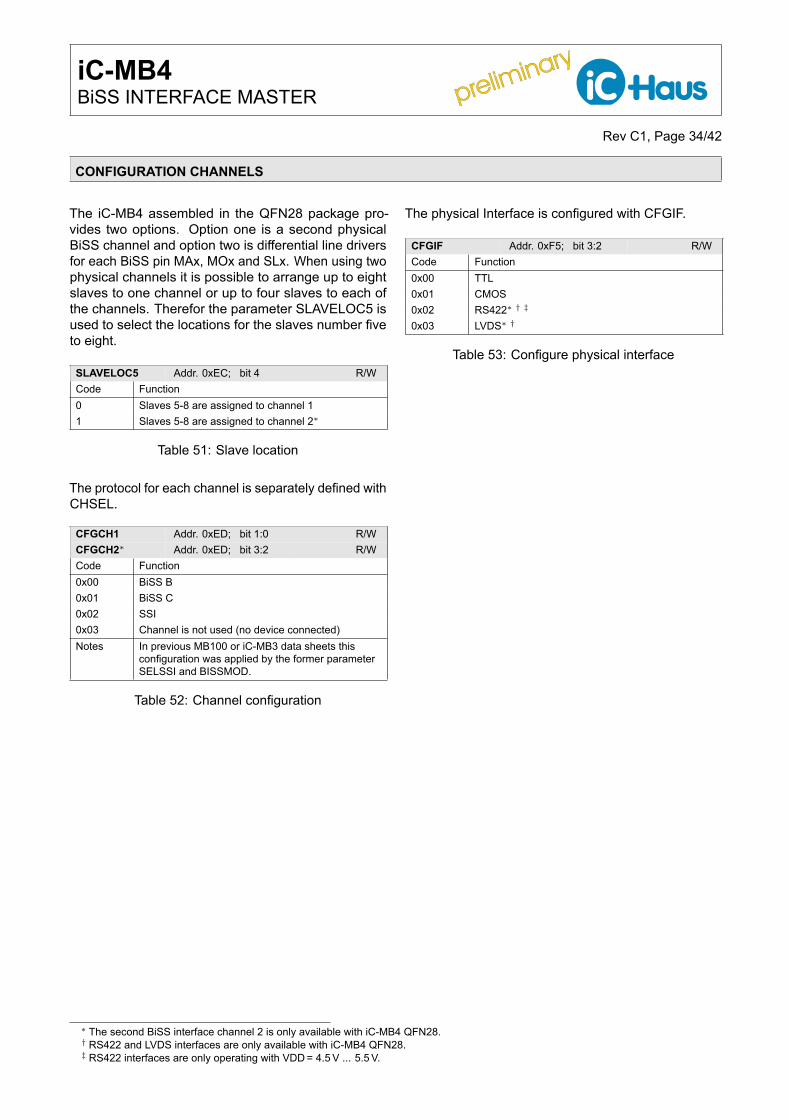
The iC-MB4 assembled in the QFN28 package pro-vides two options. Option one is a second physicalBiSS channel and option two is differential line driversfor each BiSS pin MAx, MOx and SLx. When using twophysical channels it is possible to arrange up to eightslaves to one channel or up to four slaves to each ofthe channels. Therefor the parameter SLAVELOC5 isused to select the locations for the slaves number fiveto eight.
SLAVELOC5 Addr. 0xEC; bit 4 R/WCode Function0 Slaves 5-8 are assigned to channel 11 Slaves 5-8 are assigned to channel 2∗
Table 51: Slave location
The protocol for each channel is separately defined withCHSEL.
CFGCH1 Addr. 0xED; bit 1:0 R/WCFGCH2∗ Addr. 0xED; bit 3:2 R/WCode Function0x00 BiSS B0x01 BiSS C0x02 SSI0x03 Channel is not used (no device connected)Notes In previous MB100 or iC-MB3 data sheets this
configuration was applied by the former parameterSELSSI and BISSMOD.
Table 52: Channel configuration
The physical Interface is configured with CFGIF.
CFGIF Addr. 0xF5; bit 3:2 R/WCode Function0x00 TTL0x01 CMOS0x02 RS422∗ † ‡
0x03 LVDS∗ †
Table 53: Configure physical interface
∗ The second BiSS interface channel 2 is only available with iC-MB4 QFN28.† RS422 and LVDS interfaces are only available with iC-MB4 QFN28.‡ RS422 interfaces are only operating with VDD = 4.5 V ... 5.5 V.
preliminary
preliminary iC-MB4BiSS INTERFACE MASTER
Rev C1, Page 35/42
STATUS INFORMATION
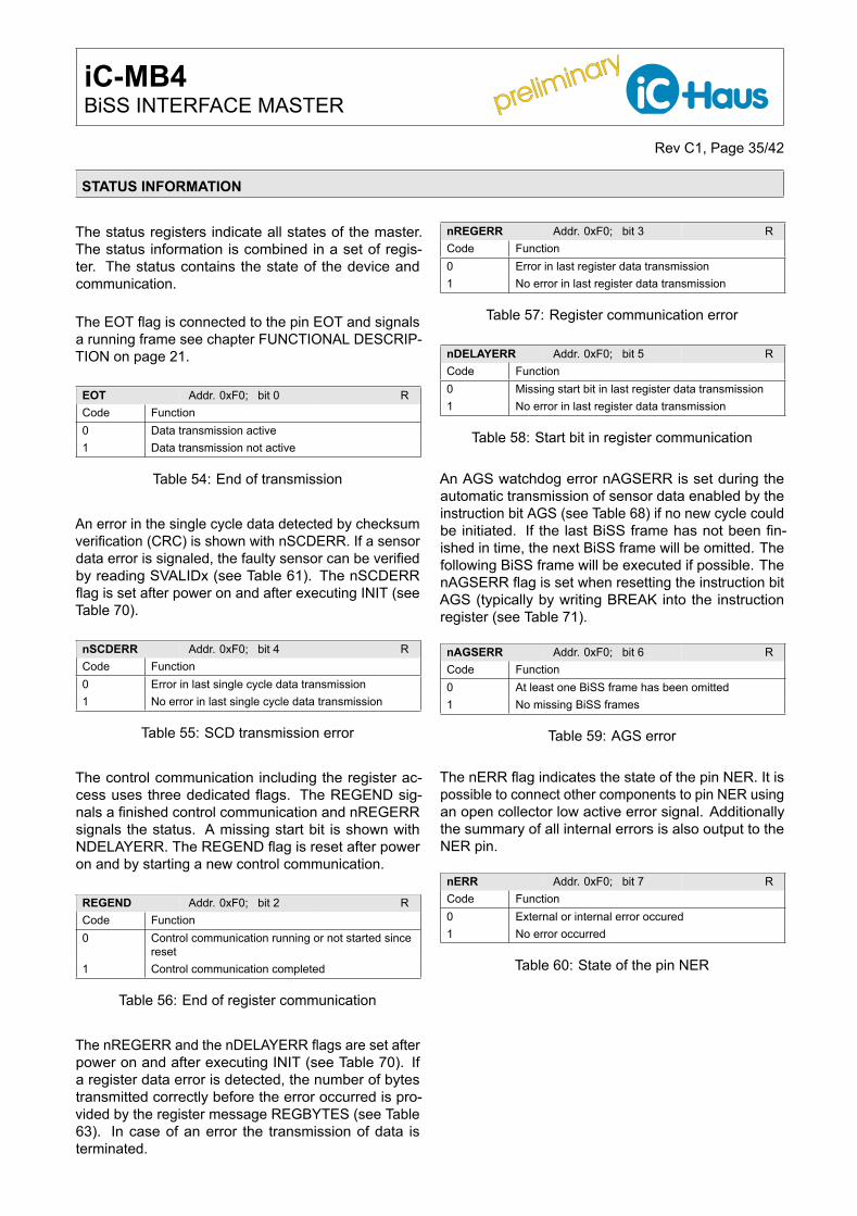
The status registers indicate all states of the master.The status information is combined in a set of regis-ter. The status contains the state of the device andcommunication.
The EOT flag is connected to the pin EOT and signalsa running frame see chapter FUNCTIONAL DESCRIP-TION on page 21.
EOT Addr. 0xF0; bit 0 RCode Function0 Data transmission active1 Data transmission not active
Table 54: End of transmission
An error in the single cycle data detected by checksumverification (CRC) is shown with nSCDERR. If a sensordata error is signaled, the faulty sensor can be verifiedby reading SVALIDx (see Table 61). The nSCDERRflag is set after power on and after executing INIT (seeTable 70).
nSCDERR Addr. 0xF0; bit 4 RCode Function0 Error in last single cycle data transmission1 No error in last single cycle data transmission
Table 55: SCD transmission error
The control communication including the register ac-cess uses three dedicated flags. The REGEND sig-nals a finished control communication and nREGERRsignals the status. A missing start bit is shown withNDELAYERR. The REGEND flag is reset after poweron and by starting a new control communication.
REGEND Addr. 0xF0; bit 2 RCode Function0 Control communication running or not started since
reset1 Control communication completed
Table 56: End of register communication
The nREGERR and the nDELAYERR flags are set afterpower on and after executing INIT (see Table 70). Ifa register data error is detected, the number of bytestransmitted correctly before the error occurred is pro-vided by the register message REGBYTES (see Table63). In case of an error the transmission of data isterminated.
nREGERR Addr. 0xF0; bit 3 RCode Function0 Error in last register data transmission1 No error in last register data transmission
Table 57: Register communication error
nDELAYERR Addr. 0xF0; bit 5 RCode Function0 Missing start bit in last register data transmission1 No error in last register data transmission
Table 58: Start bit in register communication
An AGS watchdog error nAGSERR is set during theautomatic transmission of sensor data enabled by theinstruction bit AGS (see Table 68) if no new cycle couldbe initiated. If the last BiSS frame has not been fin-ished in time, the next BiSS frame will be omitted. Thefollowing BiSS frame will be executed if possible. ThenAGSERR flag is set when resetting the instruction bitAGS (typically by writing BREAK into the instructionregister (see Table 71).
nAGSERR Addr. 0xF0; bit 6 RCode Function0 At least one BiSS frame has been omitted1 No missing BiSS frames
Table 59: AGS error
The nERR flag indicates the state of the pin NER. It ispossible to connect other components to pin NER usingan open collector low active error signal. Additionallythe summary of all internal errors is also output to theNER pin.
nERR Addr. 0xF0; bit 7 RCode Function0 External or internal error occured1 No error occurred
Table 60: State of the pin NER
preliminary
preliminary iC-MB4BiSS INTERFACE MASTER
Rev C1, Page 36/42
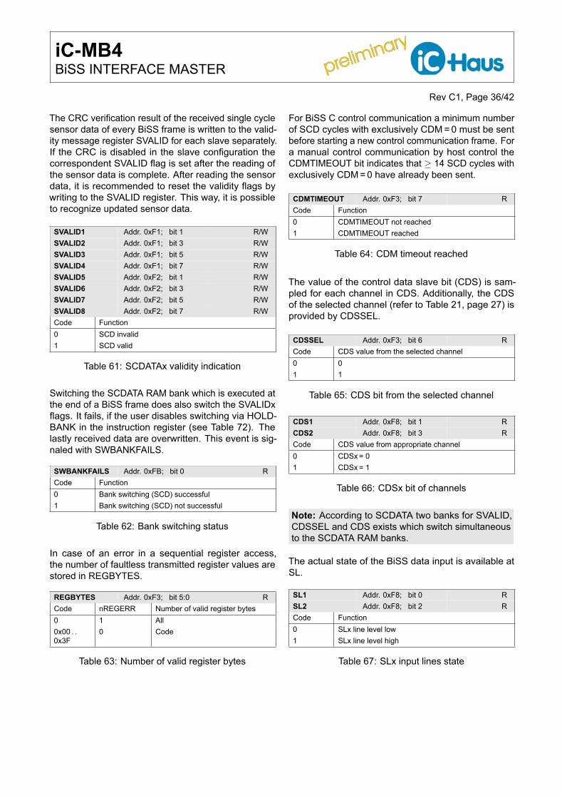
The CRC verification result of the received single cyclesensor data of every BiSS frame is written to the valid-ity message register SVALID for each slave separately.If the CRC is disabled in the slave configuration thecorrespondent SVALID flag is set after the reading ofthe sensor data is complete. After reading the sensordata, it is recommended to reset the validity flags bywriting to the SVALID register. This way, it is possibleto recognize updated sensor data.
SVALID1 Addr. 0xF1; bit 1 R/WSVALID2 Addr. 0xF1; bit 3 R/WSVALID3 Addr. 0xF1; bit 5 R/WSVALID4 Addr. 0xF1; bit 7 R/WSVALID5 Addr. 0xF2; bit 1 R/WSVALID6 Addr. 0xF2; bit 3 R/WSVALID7 Addr. 0xF2; bit 5 R/WSVALID8 Addr. 0xF2; bit 7 R/WCode Function0 SCD invalid1 SCD valid
Table 61: SCDATAx validity indication
Switching the SCDATA RAM bank which is executed atthe end of a BiSS frame does also switch the SVALIDxflags. It fails, if the user disables switching via HOLD-BANK in the instruction register (see Table 72). Thelastly received data are overwritten. This event is sig-naled with SWBANKFAILS.
SWBANKFAILS Addr. 0xFB; bit 0 RCode Function0 Bank switching (SCD) successful1 Bank switching (SCD) not successful
Table 62: Bank switching status
In case of an error in a sequential register access,the number of faultless transmitted register values arestored in REGBYTES.
REGBYTES Addr. 0xF3; bit 5:0 RCode nREGERR Number of valid register bytes0 1 All0x00 . .0x3F
0 Code
Table 63: Number of valid register bytes
For BiSS C control communication a minimum numberof SCD cycles with exclusively CDM = 0 must be sentbefore starting a new control communication frame. Fora manual control communication by host control theCDMTIMEOUT bit indicates that ≥ 14 SCD cycles withexclusively CDM = 0 have already been sent.
CDMTIMEOUT Addr. 0xF3; bit 7 RCode Function0 CDMTIMEOUT not reached1 CDMTIMEOUT reached
Table 64: CDM timeout reached
The value of the control data slave bit (CDS) is sam-pled for each channel in CDS. Additionally, the CDSof the selected channel (refer to Table 21, page 27) isprovided by CDSSEL.
CDSSEL Addr. 0xF3; bit 6 RCode CDS value from the selected channel0 01 1
Table 65: CDS bit from the selected channel
CDS1 Addr. 0xF8; bit 1 RCDS2 Addr. 0xF8; bit 3 RCode CDS value from appropriate channel0 CDSx = 01 CDSx = 1
Table 66: CDSx bit of channels
Note: According to SCDATA two banks for SVALID,CDSSEL and CDS exists which switch simultaneousto the SCDATA RAM banks.
The actual state of the BiSS data input is available atSL.
SL1 Addr. 0xF8; bit 0 RSL2 Addr. 0xF8; bit 2 RCode Function0 SLx line level low1 SLx line level high
Table 67: SLx input lines state
preliminary
preliminary iC-MB4BiSS INTERFACE MASTER
Rev C1, Page 37/42
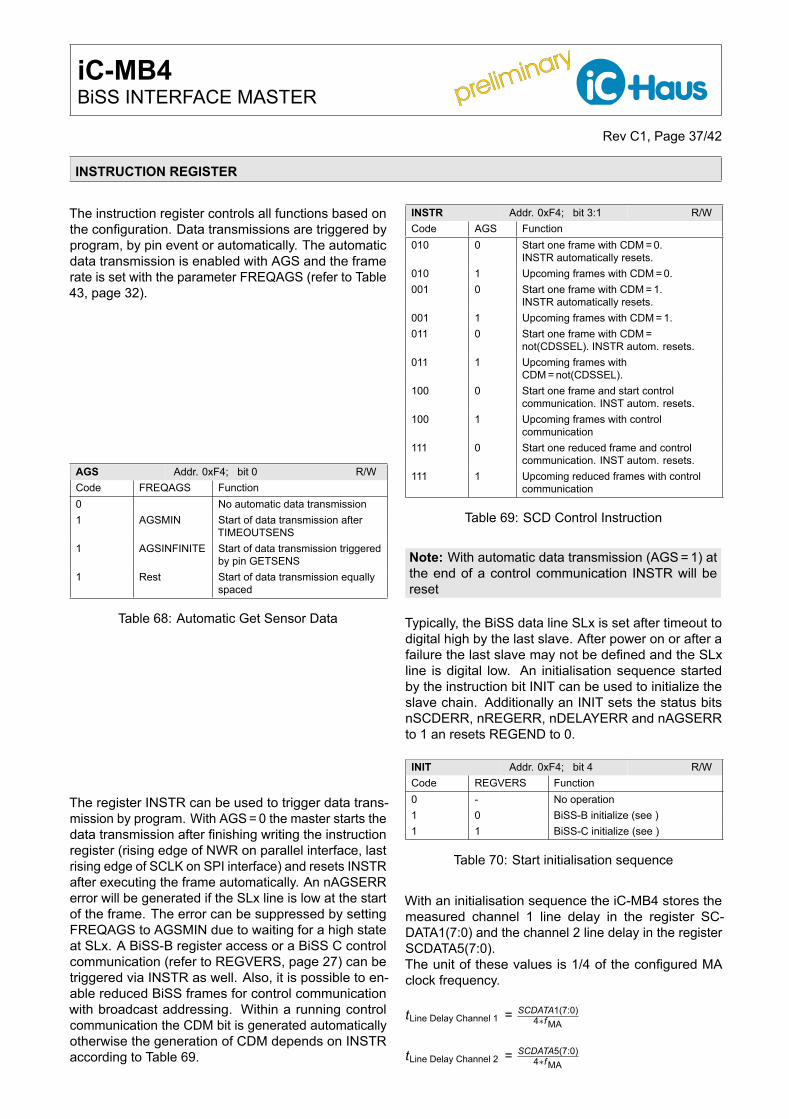
INSTRUCTION REGISTER
The instruction register controls all functions based onthe configuration. Data transmissions are triggered byprogram, by pin event or automatically. The automaticdata transmission is enabled with AGS and the framerate is set with the parameter FREQAGS (refer to Table43, page 32).
AGS Addr. 0xF4; bit 0 R/WCode FREQAGS Function0 No automatic data transmission1 AGSMIN Start of data transmission after
TIMEOUTSENS1 AGSINFINITE Start of data transmission triggered
by pin GETSENS1 Rest Start of data transmission equally
spaced
Table 68: Automatic Get Sensor Data
The register INSTR can be used to trigger data trans-mission by program. With AGS = 0 the master starts thedata transmission after finishing writing the instructionregister (rising edge of NWR on parallel interface, lastrising edge of SCLK on SPI interface) and resets INSTRafter executing the frame automatically. An nAGSERRerror will be generated if the SLx line is low at the startof the frame. The error can be suppressed by settingFREQAGS to AGSMIN due to waiting for a high stateat SLx. A BiSS-B register access or a BiSS C controlcommunication (refer to REGVERS, page 27) can betriggered via INSTR as well. Also, it is possible to en-able reduced BiSS frames for control communicationwith broadcast addressing. Within a running controlcommunication the CDM bit is generated automaticallyotherwise the generation of CDM depends on INSTRaccording to Table 69.
INSTR Addr. 0xF4; bit 3:1 R/WCode AGS Function010 0 Start one frame with CDM = 0.
INSTR automatically resets.010 1 Upcoming frames with CDM = 0.001 0 Start one frame with CDM = 1.
INSTR automatically resets.001 1 Upcoming frames with CDM = 1.011 0 Start one frame with CDM =
not(CDSSEL). INSTR autom. resets.011 1 Upcoming frames with
CDM = not(CDSSEL).100 0 Start one frame and start control
communication. INST autom. resets.100 1 Upcoming frames with control
communication111 0 Start one reduced frame and control
communication. INST autom. resets.111 1 Upcoming reduced frames with control
communication
Table 69: SCD Control Instruction
Note: With automatic data transmission (AGS = 1) atthe end of a control communication INSTR will bereset
Typically, the BiSS data line SLx is set after timeout todigital high by the last slave. After power on or after afailure the last slave may not be defined and the SLxline is digital low. An initialisation sequence startedby the instruction bit INIT can be used to initialize theslave chain. Additionally an INIT sets the status bitsnSCDERR, nREGERR, nDELAYERR and nAGSERRto 1 an resets REGEND to 0.
INIT Addr. 0xF4; bit 4 R/WCode REGVERS Function0 - No operation1 0 BiSS-B initialize (see )1 1 BiSS-C initialize (see )
Table 70: Start initialisation sequence
With an initialisation sequence the iC-MB4 stores themeasured channel 1 line delay in the register SC-DATA1(7:0) and the channel 2 line delay in the registerSCDATA5(7:0).The unit of these values is 1/4 of the configured MAclock frequency.
tLine Delay Channel 1 = SCDATA1(7:0)4∗fMA
tLine Delay Channel 2 = SCDATA5(7:0)4∗fMA
preliminary
preliminary iC-MB4BiSS INTERFACE MASTER
Rev C1, Page 38/42
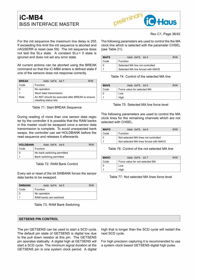
For the init sequence the maximum line delay is 255.If exceeding this limit the init sequence is aborted andnAGSERR is reset (see 59). The init sequence doesnot test the SLx state. A constant SLx = 0 state isignored and does not set any error state.
All current actions can be aborted using the BREAKcommand so that the iC-MB4 enters a defined state ifone of the sensors does not response correctly.
BREAK Addr. 0xF4; bit 7 R/WCode Function0 No operation1 Abort data transmissionNote An INIT should be executed after BREAK to ensure
resetting status bits
Table 71: Start BREAK Sequence
During reading of more than one sensor data regis-ter by the controller it is possible that the RAM banksin the master could be swapped once a sensor datatransmission is complete. To avoid unexpected bankswaps, the controller can set HOLDBANK before theread sequence and releases it afterwards.
HOLDBANK Addr. 0xF4; bit 6 R/WCode Function0 No bank switching permitted1 Bank switching permitted
Table 72: RAM Bank Control
Every set or reset of the bit SWBANK forces the sensordata banks to be swapped.
SWBANK Addr. 0xF4; bit 5 R/WCode Function0 No operation1 RAM banks are switched
Table 73: RAM Bank Switching
The following parameters are used to control the the MAclock line which is selected with the parameter CHSEL(see Table 21).
MAFS Addr. 0xF5; bit 4 R/WCode Function0 Selected MA line not controlled1 Selected MA line forced with MAVS
Table 74: Control of the selected MA line
MAVS Addr. 0xF5; bit 5 R/WCode Force value for selected MA0 Low1 High
Table 75: Selected MA line force level
The following parameters are used to control the MAclock lines for the remaining channels which are notselected with CHSEL.
MAFO Addr. 0xF5; bit 6 R/WCode Function0 Not selected MA lines not controlled1 Not selected MA lines forced with MAVO
Table 76: Control of the not selected MA line
MAVO Addr. 0xF5; bit 7 R/WCode Force value for not selected MA0 Low1 High
Table 77: Not selected MA lines force level
GETSENS PIN CONTROL
The pin GETSENS can be used to start a SCD cycle.The default pin state of GETSENS is digital low dueto the pull down resistor at this pin. The GETSENSpin operates statically: A digital high at GETSENS willstart a SCD cycle. The minimum signal duration at theGETSENS pin is one system clock period. A digital
high that is longer than the SCD cycle will restart thenext SCD cycle.
For high precision capturing it is recommended to usea system clock based GETSENS digital high pulse.

preliminary
preliminary iC-MB4BiSS INTERFACE MASTER
Rev C1, Page 39/42
DESIGN REVIEW
Function Notes
iC-MB4 Z1No. Function, Parameter/Code Description and application notes1 MO_BUSY Control communication max fail, if MO_BUSY /= 0 and output MO is not connected
to slave input SLI.2 Actuator data Transmission of actuator data on both channels with different SCD length fail, if
CDM = 0.3 BiSS C initialize sequence Line delay measurement fails, if line delay of one channel is bigger than line delay
plus timeout of the other channel.
Table 78: Notes on chip functions regarding iC-MB4 chip release Z1.
All listed chip functions are adjusted with iC-MB4 chip release Y.
preliminary
preliminary iC-MB4BiSS INTERFACE MASTER
Rev C1, Page 40/42
REVISION HISTORY
Rel. Rel. Date∗ Chapter Modification PageA1 14-06-24 Initial Release.
Rel. Rel. Date∗ Chapter Modification PageB1 14-11-20 PACKAGING INFORMATION Function text on pin 25 NWR_E swapped with Function text on pin 26 NRD_RNW:
• NWR_E: Read Input, active low (Intel) Read/Not-Write Select Input (Motorola)• NRD_RNW: Write Input, active low (Intel) Enable Input, active high (Motorola)
4
ELECTRICALCHARACTERISTICS
Vc()hi Clamp Voltage hi MAX updated from 1.65 V to 1.75 V 8
ELECTRICALCHARACTERISTICS
f(CLKI) Oscillator Clock Frequency VDD = 3.0 V ... 3.6 V MAX updated from 20 MHz to22 MHz
9
FUNCTIONAL DESCRIPTION INIT = 1 updated 21INSTRUCTION REGISTER ”All configuration parameter must be stable during data transmission” added 28CONFIGURATION MASTER AUTOMATIC REQUEST FOR SENSOR DATA moved into chapter CONFIGURATION
MASTER29
CONFIGURATION CHANNEL CFGIF footnote added: RS422 interfaces are only operatable with VDD = 4.5 V ... 5.5 V 31CONFIGURATION SLAVE Slave Configuration CRC Verification:
• CRC for single cycle data not present, CRC verification deactivated, SELCRCSx = 0b0• CRC polynomial(7:1) in SCRCPOLYx SELCRCSx = 0b1 not applicable with CRC poly-
nomial SCRCPOLYx(7:1) = 0x00• CRC polynomial 0x00 not applicable with SELCRCSx = 0b1• Other CRC lengths in SCRCLENx are not permitted with SELCRCSx = 0b0
32
STATUS INFORMATION 1 Bit address of nDELAYERR 0xF0 updated to 5 35APPLICATION DESIGNTRANSFER FROM iC-MB3TSSOP24 TO iC-MB4 TSSOP24
Disabling SCD CRC verification To deactivate the SCD CRC verification select:
• SELCRCSx = 0b0• CRC bit length in SCRCLENx = 0• Extend the SCDLEN by the length of the present CRC that is subject to be ignored
A CRC polynomial SCRCPOLYx = 0x00 is not applicable with SELCRCSx = 0b1.
38
DESIGN REVIEW Chapter DESIGN REVIEW added 39FUNCTIONAL DESCRIPTION Measuring the line delay on channel 1 and channel 2, measuring unit added 21
Rel. Rel. Date∗ Chapter Modification PageB2 2015-07-07 DESCRIPTION BiSS BUA added 2
FUNCTIONAL DESCRIPTION Maximum line delay while INIT = 255, overflow abort and AGERR is set 21INSTRUCTION REGISTER All configuration parameter must be stable during SCD data transmission 28
preliminary
preliminary iC-MB4BiSS INTERFACE MASTER
Rev C1, Page 41/42
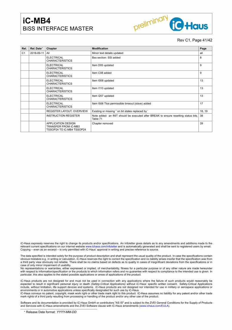
Rel. Rel. Date∗ Chapter Modification PageC1 2018-09-11 All Minor text details updated all
ELECTRICALCHARACTERISTICS
Bxx section: SSI added 8
ELECTRICALCHARACTERISTICS
Item D05 updated 9
ELECTRICALCHARACTERISTICS
Item C08 added 9
ELECTRICALCHARACTERISTICS
Item I008 updated 13
ELECTRICALCHARACTERISTICS
Item I110 updated 13
ELECTRICALCHARACTERISTICS
Item I207 updated 13
ELECTRICALCHARACTERISTICS
Item I506 Ttos permissible timeout (slave) added 17
REGISTER LAYOUT, OVERVIEW Existing or missing ” on bit states replaced by ’ 18, 19INSTRUCTION REGISTER Note added: an INIT should be executed after BREAK to ensure resetting status bits,
Table 7138
APPLICATION DESIGNTRANSFER FROM iC-MB3TSSOP24 TO iC-MB4 TSSOP24
Chapter removed 39
iC-Haus expressly reserves the right to change its products and/or specifications. An Infoletter gives details as to any amendments and additions made to therelevant current specifications on our internet website www.ichaus.com/infoletter and is automatically generated and shall be sent to registered users by email.Copying – even as an excerpt – is only permitted with iC-Haus’ approval in writing and precise reference to source.
The data specified is intended solely for the purpose of product description and shall represent the usual quality of the product. In case the specifications containobvious mistakes e.g. in writing or calculation, iC-Haus reserves the right to correct the specification and no liability arises insofar that the specification was froma third party view obviously not reliable. There shall be no claims based on defects as to quality in cases of insignificant deviations from the specifications or incase of only minor impairment of usability.No representations or warranties, either expressed or implied, of merchantability, fitness for a particular purpose or of any other nature are made hereunderwith respect to information/specification or the products to which information refers and no guarantee with respect to compliance to the intended use is given. Inparticular, this also applies to the stated possible applications or areas of applications of the product.
iC-Haus products are not designed for and must not be used in connection with any applications where the failure of such products would reasonably beexpected to result in significant personal injury or death (Safety-Critical Applications) without iC-Haus’ specific written consent. Safety-Critical Applicationsinclude, without limitation, life support devices and systems. iC-Haus products are not designed nor intended for use in military or aerospace applications orenvironments or in automotive applications unless specifically designated for such use by iC-Haus.iC-Haus conveys no patent, copyright, mask work right or other trade mark right to this product. iC-Haus assumes no liability for any patent and/or other trademark rights of a third party resulting from processing or handling of the product and/or any other use of the product.
Software and its documentation is provided by iC-Haus GmbH or contributors "AS IS" and is subject to the ZVEI General Conditions for the Supply of Productsand Services with iC-Haus amendments and the ZVEI Software clause with iC-Haus amendments (www.ichaus.com/EULA).
∗ Release Date format: YYYY-MM-DD

preliminary
preliminary iC-MB4BiSS INTERFACE MASTER
Rev C1, Page 42/42
ORDERING INFORMATION
Type Package Order Designation
iC-MB4 TSSOP24 iC-MB4 TSSOP24
iC-MB4 QFN28-5x5 iC-MB4 QFN28-5x5
EvaluationBoard
iC-MB4 EVAL MB4_1D
Please send your purchase orders to our order handling team:
Fax: +49 (0) 61 35 - 92 92 - 692E-Mail: [email protected]
For technical support, information about prices and terms of delivery please contact:
iC-Haus GmbH Tel.: +49 (0) 61 35 - 92 92 - 0Am Kuemmerling 18 Fax: +49 (0) 61 35 - 92 92 - 192D-55294 Bodenheim Web: http://www.ichaus.comGERMANY E-Mail: [email protected]
Appointed local distributors: http://www.ichaus.com/sales_partners