Embed Size (px)
Citation preview
I2CbusspecificationsfortheCMStracker2S&PSmodules
V2.0
21/4/2016
2
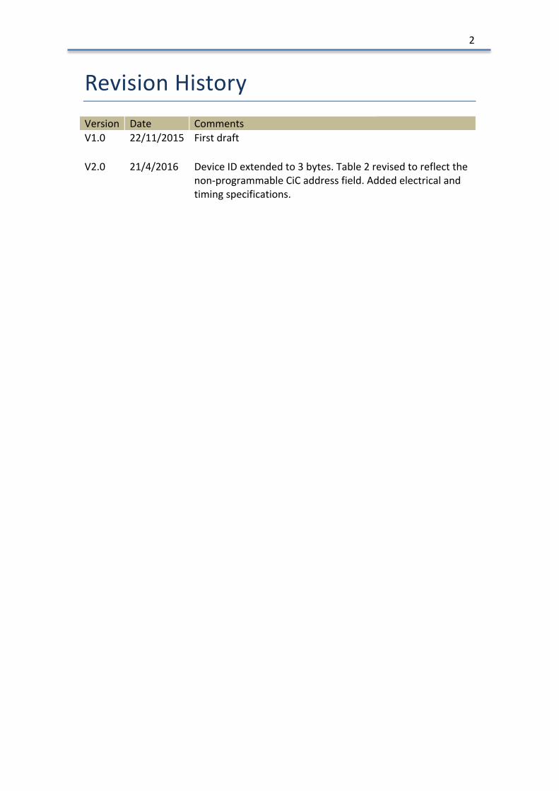
RevisionHistoryVersion Date CommentsV1.0 22/11/2015 Firstdraft
V2.0 21/4/2016 DeviceIDextendedto3bytes.Table2revisedtoreflectthe
non-programmableCiCaddressfield.Addedelectricalandtimingspecifications.
3
1 INTRODUCTIONThe present document discusses the implementation of the I2C serial
communicationbusintheCMSOuterTrackerPS(Pixel-Stip)&2S(Strip-Strip)modules.TheuseoftheI2Cbusistomonitorandcontroltheoperationofthefront-endASICspopulatingthePS&2Smodules.Theaimofthedocumentisto present guidelines for the development of I2C circuitry of the front-endASICs.
ItshouldbenotedthatonlyasubsetoffeaturesoftheI2CBusstandardarenecessarytosupportthefunctionalityoftheASICsofthePS&2Smodulesand therefore the design guidelines are limited to these features. Particularattention is taken not to violate the I2C Bus standard for the supportedfeatures.
TheI2CfeaturesforthePS&2Smodulesinclude:
q CompliancetothePhilipsSemiconductorI2Cspecificationv2.1q Singlemasterbusq 7-bitaddressingq Single-byte&Multi-bytetransfers
n Needtodefinemaximumnumberofbytesq GeneralCallAddressing
n Usewithinachipfamily(CBC,MPA,SSA,CiC)n Setoperationalmodes,testpulseamplitude&delay,latency
valueincommonforallchipsn CBC2“broadcastaddressscheme”(1111111+data+data+….)
doesnotconformtothe“GeneralCallAddressing”formatbutcanbegeneratedusingstandardmulti-byteWritetransfers(seenextslide)
q 100KHz,400KHz&1MHzbitrate
4
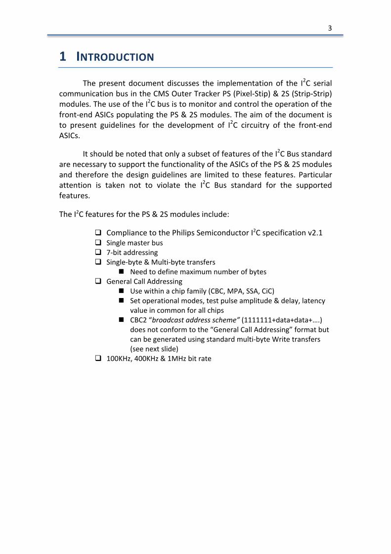
1.1 I2CBusTopologyThe I2C Bus Topology for the PS and 2S is shown in Figure 1. The optical linkcommunicationASIC;namelythelpGBT(lowpowerGigaBitTransceiver)isequippedwithtwoindependentI2CmasterinterfacesthatrealizetwoindependentI2Cbusses.ThelpGBTI2Cmasterinterfaceistheonlymasterinterfacepermittedtoconnectonthe bus. All front-end ASICs; namely the MPA, the SSA, the CiC, the CBC, mustimplementanI2CSlaveinterface.GenerationofclocksignalsontheI2C-busisalwaystheresponsibilityofthemasterdevice.
Figure1I2CBustopologyforPSand2Smodules.
1.2 SDA&SCLSignalsBothSDAandSCLarebidirectionallines,connectedtoapositivesupplyvoltage
viaacurrent-sourceorpull-upresistor.Whenthebus is free,both linesareHIGH.The output stages of devices connected to the bus must have an open-drain toperformthewired-ANDfunction.DataontheI2C-buscanbetransferredatratesofup to100kbit/s in theStandard-mode,up to400kbit/s in theFast-mode,up to1Mbit/s in Fast-mode Plus. The bus capacitance limits the number of interfacesconnectedtothebus.Forasinglemasterapplication,themaster’sSCLoutputcanbeapush-pulldriverdesignoranopen-draindriverdesignwithanexternalpull-upresistor.Therearenoslavedevicesonthebuswhichwouldstretchtheclock.

5
Figure2I2Cbusconnectivity
1.3 BusclearIntheunlikelyeventwheretheclock(SCL)isstuckLOW,thepreferentialprocedureistoresetthebususingtheHWresetsignaliftheI2CdeviceshaveHWresetinputs.IftheI2CdevicesdonothaveHWresetinputs,cyclepowertothedevicestoactivatethemandatoryinternalPower-OnReset(POR)circuit.If thedata line (SDA) is stuck LOW, themaster should sendnineclockpulses.ThedevicethatheldthebusLOWshouldreleaseitsometimewithinthosenineclocks.Ifnot,thenusetheHWresetorcyclepowertoclearthebus.ThemasterI2Cmustbeabletogeneratethis“busclear”sequence.
SDA
SCL
VDD = 1.2V
VDD = 1.2VVDD = 1.2V VDD = 1.2V
lpGBTI2C master
FE ASICI2C slave
FE ASICI2C slave
6
2 DATATRANSFERPROTOCOL
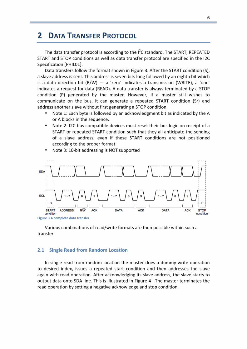
ThedatatransferprotocolisaccordingtotheI2Cstandard.TheSTART,REPEATEDSTARTandSTOPconditionsaswellasdatatransferprotocolarespecifiedintheI2CSpecification[PHIL01].
DatatransfersfollowtheformatshowninFigure3.AftertheSTARTcondition(S),aslaveaddressissent.Thisaddressissevenbitslongfollowedbyaneighthbitwhichis a data direction bit (R/W)— a ‘zero’ indicates a transmission (WRITE), a ‘one’indicatesarequestfordata(READ).AdatatransferisalwaysterminatedbyaSTOPcondition (P) generated by the master. However, if a master still wishes tocommunicate on the bus, it can generate a repeated START condition (Sr) andaddressanotherslavewithoutfirstgeneratingaSTOPcondition.
• Note1:EachbyteisfollowedbyanacknowledgmentbitasindicatedbytheAorAblocksinthesequence.
• Note2:I2C-buscompatibledevicesmustresettheirbuslogiconreceiptofaSTARTorrepeatedSTARTconditionsuchthattheyallanticipatethesendingof a slave address, even if these START conditions are not positionedaccordingtotheproperformat.
• Note3:10-bitaddressingisNOTsupported
Figure3Acompletedatatransfer
Variouscombinationsofread/writeformatsarethenpossiblewithinsuchatransfer.
2.1 SingleReadfromRandomLocation
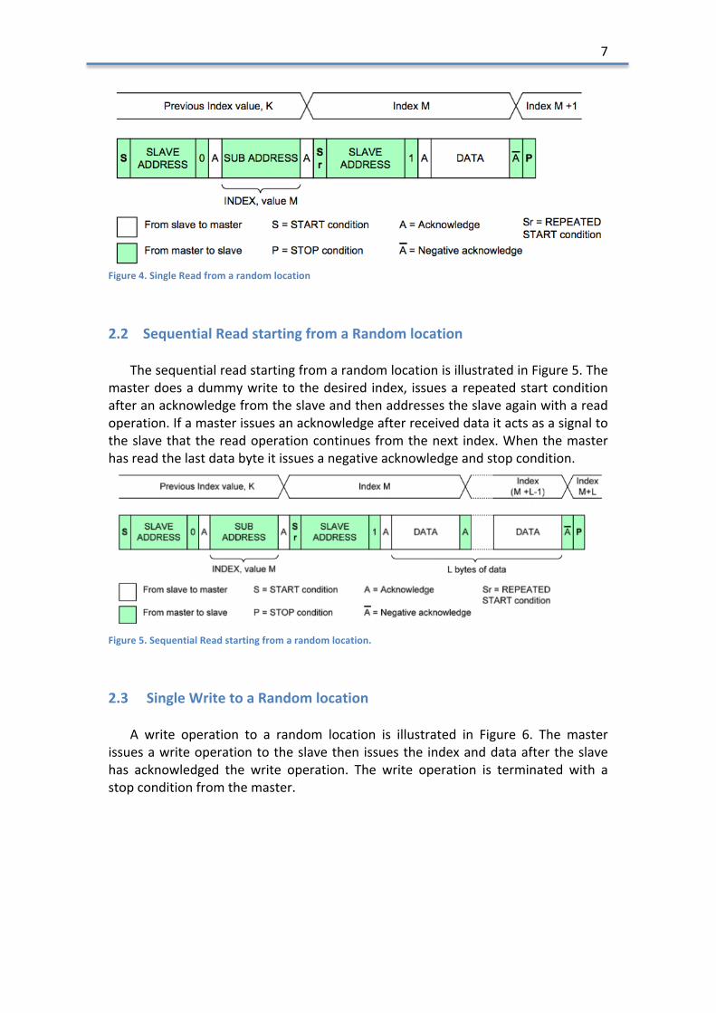
Insinglereadfromrandomlocationthemasterdoesadummywriteoperationto desired index, issues a repeated start condition and then addresses the slaveagainwithreadoperation.Afteracknowledgingitsslaveaddress,theslavestartstooutputdataontoSDAline.ThisisillustratedinFigure4.Themasterterminatesthereadoperationbysettinganegativeacknowledgeandstopcondition.
7
Figure4.SingleReadfromarandomlocation
2.2 SequentialReadstartingfromaRandomlocation
ThesequentialreadstartingfromarandomlocationisillustratedinFigure5.Themasterdoesadummywritetothedesiredindex, issuesarepeatedstartconditionafteranacknowledgefromtheslaveandthenaddressestheslaveagainwithareadoperation.Ifamasterissuesanacknowledgeafterreceiveddataitactsasasignaltotheslavethatthereadoperationcontinuesfromthenext index.Whenthemasterhasreadthelastdatabyteitissuesanegativeacknowledgeandstopcondition.
Figure5.SequentialReadstartingfromarandomlocation.
2.3 SingleWritetoaRandomlocation
A write operation to a random location is illustrated in Figure 6. The masterissuesawriteoperationtotheslavethenissuesthe indexanddataaftertheslavehas acknowledged the write operation. The write operation is terminated with astopconditionfromthemaster.
8
Figure6.SingleWriteoperationtoarandomlocation.
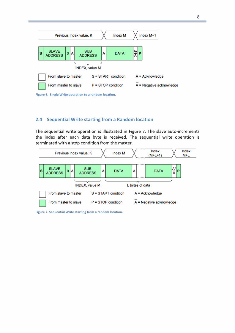
2.4 SequentialWritestartingfromaRandomlocationThesequentialwriteoperation is illustrated inFigure7.Theslaveauto-incrementsthe index after each data byte is received. The sequential write operation isterminatedwithastopconditionfromthemaster.
Figure7.SequentialWritestartingfromarandomlocation.
9
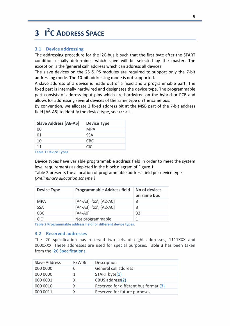
3 I2CADDRESSSPACE3.1 DeviceaddressingTheaddressingprocedurefortheI2C-busissuchthatthefirstbyteaftertheSTARTcondition usually determines which slave will be selected by the master. Theexceptionisthe‘generalcall’addresswhichcanaddressalldevices.The slave devices on the 2S& PSmodules are required to support only the 7-bitaddressingmode.The10-bitaddressingmodeisnotsupported.A slave address of a device ismade out of a fixed and a programmable part. Thefixedpartisinternallyhardwiredanddesignatesthedevicetype.Theprogrammablepart consists of address inputpinswhich arehardwiredon thehybridor PCBandallowsforaddressingseveraldevicesofthesametypeonthesamebus.Byconvention,weallocate2fixedaddressbitattheMSBpartofthe7-bitaddressfield[A6-A5]toidentifythedevicetype,seeTable1.SlaveAddress[A6-A5] DeviceType00 MPA01 SSA10 CBC11 CIC
Table1DeviceTypes
DevicetypeshavevariableprogrammableaddressfieldinordertomeetthesystemlevelrequirementsasdepictedintheblockdiagramofFigure1.Table2presentstheallocationofprogrammableaddressfieldperdevicetype(Preliminaryallocationscheme.)DeviceType ProgrammableAddressfield Noofdevices
onsamebusMPA [A4-A3]=’xx’,[A2-A0] 8SSA [A4-A3]=’xx’,[A2-A0] 8CBC [A4-A0] 32CIC Notprogrammable 1
Table2Programmableaddressfieldfordifferentdevicetypes.
3.2 ReservedaddressesThe I2C specification has reserved two sets of eight addresses, 1111XXX and0000XXX. These addresses are used for special purposes. Table 3 has been takenfromtheI2CSpecifications.SlaveAddress R/WBit Description0000000 0 Generalcalladdress0000000 1 STARTbyte(1)0000001 X CBUSaddress(2)0000010 X Reservedfordifferentbusformat(3)0000011 X Reservedforfuturepurposes
10
00001XX X Hs-modemastercode11110XX X 10-bitslaveaddressing11111XX X ReservedforfuturepurposesTable3I2Creservedaddresses
(1)NodeviceisallowedtoacknowledgeatthereceptionoftheSTARTbyte.(2)TheCBUSaddresshasbeenreservedtoenabletheinter-mixingofCBUScompatibleandI2C-buscompatibledevicesinthesamesystem.I2C-buscompatibledevicesarenotallowedtorespondonreceptionofthisaddress.(3)TheaddressreservedforadifferentbusformatisincludedtoenableI2Candotherprotocolstobemixed.OnlyI2C-buscompatibledevicesthatcanworkwithsuchformatsandprotocolsareallowedtorespondtothisaddress.
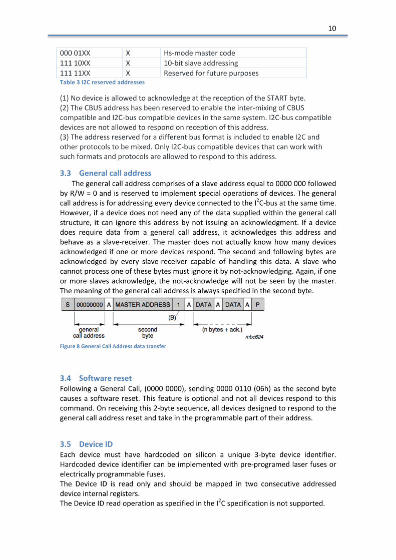
3.3 GeneralcalladdressThegeneralcalladdresscomprisesofaslaveaddressequalto0000000followed
byR/W=0andisreservedtoimplementspecialoperationsofdevices.ThegeneralcalladdressisforaddressingeverydeviceconnectedtotheI2C-busatthesametime.However,ifadevicedoesnotneedanyofthedatasuppliedwithinthegeneralcallstructure, it can ignore thisaddressbynot issuinganacknowledgment. Ifadevicedoes require data from a general call address, it acknowledges this address andbehave as a slave-receiver. Themaster doesnot actually knowhowmanydevicesacknowledgedifoneormoredevicesrespond.Thesecondandfollowingbytesareacknowledged by every slave-receiver capable of handling this data. A slave whocannotprocessoneofthesebytesmustignoreitbynot-acknowledging.Again,ifoneormoreslavesacknowledge, thenot-acknowledgewillnotbeseenby themaster.Themeaningofthegeneralcalladdressisalwaysspecifiedinthesecondbyte.
Figure8GeneralCallAddressdatatransfer
3.4 SoftwareresetFollowingaGeneralCall, (00000000),sending00000110(06h)asthesecondbytecausesasoftwarereset.Thisfeatureisoptionalandnotalldevicesrespondtothiscommand.Onreceivingthis2-bytesequence,alldevicesdesignedtorespondtothegeneralcalladdressresetandtakeintheprogrammablepartoftheiraddress.
3.5 DeviceIDEach device must have hardcoded on silicon a unique 3-byte device identifier.Hardcodeddeviceidentifiercanbeimplementedwithpre-programedlaserfusesorelectricallyprogrammablefuses.The Device ID is read only and should be mapped in two consecutive addresseddeviceinternalregisters.TheDeviceIDreadoperationasspecifiedintheI2Cspecificationisnotsupported.

11
12
4 ELECTRICALSPECIFICATIONSANDTIMINGFORI/OSTAGES
The presented electrical specifications depict the guidelines for theimplementationofI2Cbussesforthe2SandPSmodules.Thepowersupplyis1.2V.Even though the targeted bitrate is 1000 kbit/sec, the document gives timingspecificationsalsoforfall-backbitratesof400kbit/secand100kbit/sec.Itisadvicedthatalldevicesusedinthe2SandPSsystemsarecompatibleforallthreebit-rates.
4.1 DCElectricalCharacteristicsTable4presentstheDCelectricalspecificationsoftheI2Cbusimplementation
forthe2SandPSmodules.Symbol Parameter Conditions VDD SupplyVoltage 1.2VVOL MaximumLowOutputVoltage Iout=6mA 0.2VVOH MaximumHighOutputVoltage Iout=-100uA VDD+0.4VVIL MaximumLowInputVoltage 0.6VVIH MinimumHighInputVoltage 1.0VIL MaximumLowSinkCurrent VOUT=0.2V 6mA
Table4DCelectricalcharacteristics
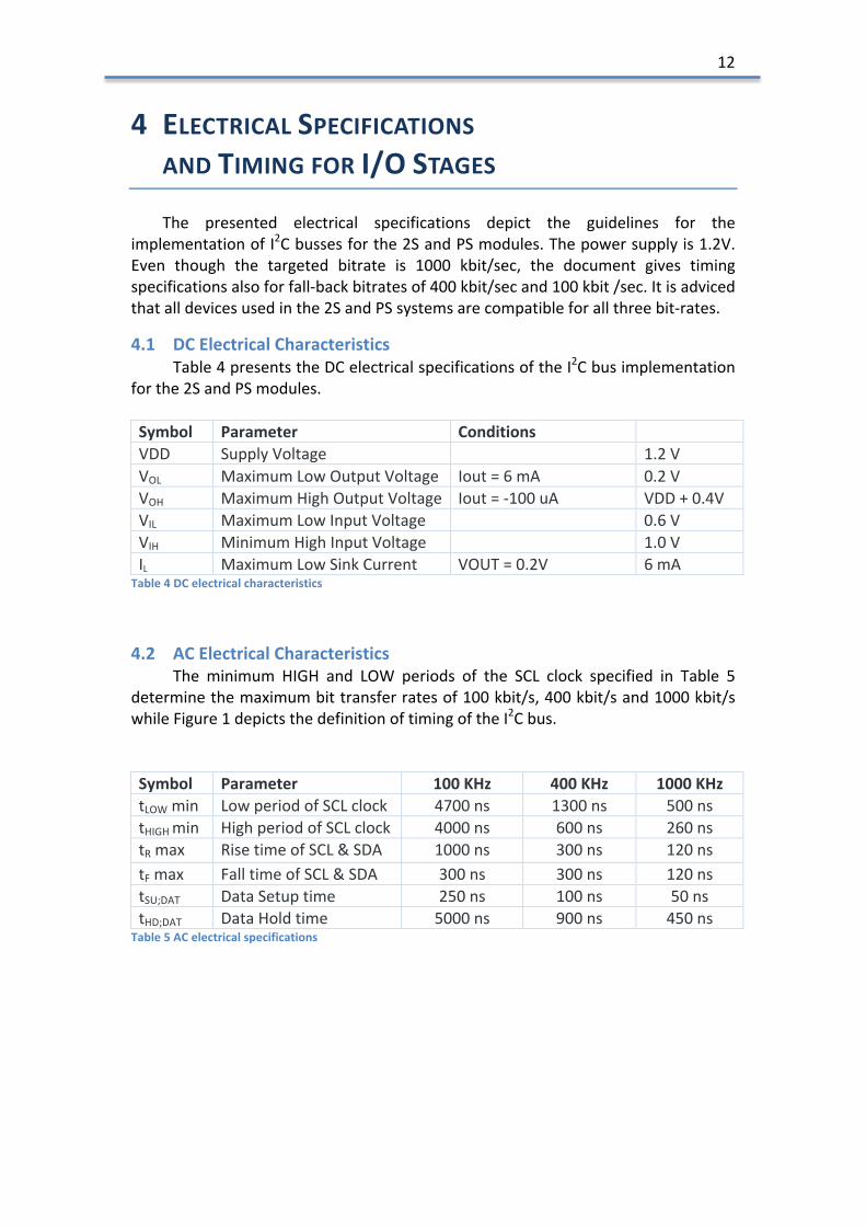
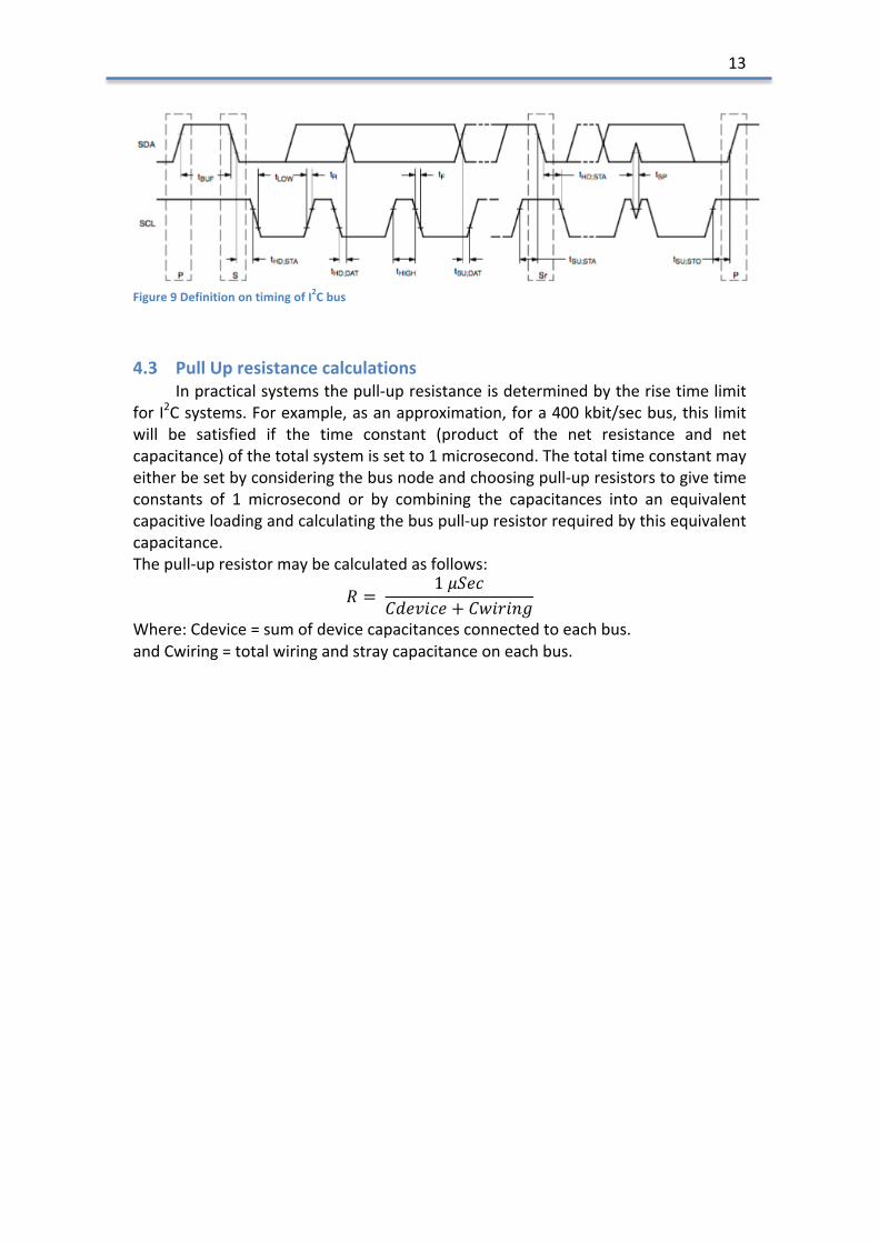
4.2 ACElectricalCharacteristicsThe minimum HIGH and LOW periods of the SCL clock specified in Table 5
determinethemaximumbittransferratesof100kbit/s,400kbit/sand1000kbit/swhileFigure1depictsthedefinitionoftimingoftheI2Cbus.
Symbol Parameter 100KHz 400KHz 1000KHztLOWmin LowperiodofSCLclock 4700ns 1300ns 500nstHIGHmin HighperiodofSCLclock 4000ns 600ns 260nstRmax RisetimeofSCL&SDA 1000ns 300ns 120nstFmax FalltimeofSCL&SDA 300ns 300ns 120nstSU;DAT DataSetuptime 250ns 100ns 50nstHD;DAT DataHoldtime 5000ns 900ns 450ns
Table5ACelectricalspecifications
13
Figure9DefinitionontimingofI2Cbus
4.3 PullUpresistancecalculationsInpracticalsystemsthepull-upresistanceisdeterminedbytherisetimelimit
forI2Csystems.Forexample,asanapproximation,fora400kbit/secbus,thislimitwill be satisfied if the time constant (product of the net resistance and netcapacitance)ofthetotalsystemissetto1microsecond.Thetotaltimeconstantmayeitherbesetbyconsideringthebusnodeandchoosingpull-upresistorstogivetimeconstants of 1 microsecond or by combining the capacitances into an equivalentcapacitiveloadingandcalculatingthebuspull-upresistorrequiredbythisequivalentcapacitance.Thepull-upresistormaybecalculatedasfollows:
𝑅 = 1𝜇𝑆𝑒𝑐
𝐶𝑑𝑒𝑣𝑖𝑐𝑒 + 𝐶𝑤𝑖𝑟𝑖𝑛𝑔
Where:Cdevice=sumofdevicecapacitancesconnectedtoeachbus.andCwiring=totalwiringandstraycapacitanceoneachbus.