Embed Size (px)
Citation preview
High efficiency excitation of plasmonic
waveguides with vertically integrated resonant
bowtie apertures
Edward C. Kinzel, Xianfan Xu*
School of Mechanical Engineering and Birck Nanotechnology Center, Purdue University, West Lafayette, IN 47907,
USA
Abstract: In recent years, many nanophotonic devices have been
developed. Much attention has been given to the waveguides carrying
surface plasmon polariton modes with subwavelength confinement and long
propagation length. However, coupling far field light into a nano structure is
a significant challenge. In this work, we present an architecture that enables
high efficiency excitation of nanoscale waveguides in the direction normal
to the waveguide. Our approach employs a bowtie aperture to provide both
field confinement and high transmission efficiency. More than six times the
power incident on the open area of the bowtie aperture can be coupled into
the waveguide. The intensity in the waveguide can be more than twenty
times higher than that of the incident light, with mode localization better
than λ2/250. The vertical excitation of waveguide allows easy integration.
The bowtie aperture/waveguide architecture presented in this work will
open up numerous possibilities for the development of nanoscale optical
systems for applications ranging from localized chemical sensing to
compact communication devices.
©2009 Optical Society of America
OCIS codes: (240.6680) Surface Plasmons; (230.7390) Waveguides planar; (130.2790) Guided
waves.
References and links
1. R. Kirchain, and L. Kimerling, “A roadmap for nanophotonics,” Nat. Photonics 1(6), 303–305 (2007).
2. E. Ozbay, “Plasmonics: merging photonics and electronics at nanoscale dimensions,” Science 311(5758),
189–193 (2006).
3. W. L. Barnes, A. Dereux, and T. W. Ebbesen, “Surface plasmon subwavelength optics,” Nature 424(6950),
824–830 (2003).
4. S. I. Bozhevolnyi, V. S. Volkov, E. Devaux, J. Y. Laluet, and T. W. Ebbesen, “Channel plasmon
subwavelength waveguide components including interferometers and ring resonators,” Nature 440(7083),
508–511 (2006).
5. H. Raether, Surface Plasmons on Smooth and Rough Surfaces and on Gratings, (Springer-Verlag, 1988).
6. J. A. Dionne, L. A. Sweatlock, and H. A. Atwater, “Plasmon slot waveguides: Towards chip-scale
propagation with subwavelength-scale localization,” Phys. Rev. B 73(3), 035407–035415 (2006).
7. R. F. Oulton, V. J. Sorger, D. A. Genov, D. F. P. Pile, and X. Zhang, “A hybrid plasmonic waveguide for
subwavelength confinement and long-range propagation,” Nat. Photonics 2(8), 496–500 (2008).
8. S. Ramo, J. R. Whinnery, and T. Van Duzer, Fields and Waves in Communication Electronics, (Wiley,
1994).
9. D. M. Pozar, Microwave Engineering, (Wiley, 2003).
10. T. A. Mandviwala, B. A. Lail, and G. D. Boreman, “Characterization of microstrip transmission lines at IR
frequencies – modeling, fabrication and measurements,” Microw. Opt. Technol. Lett. 50(5), 1232–1237
(2008).
11. A. Hosseini, H. Nejati, and Y. Massoud, “Design of a maximally flat optical low pass filter using plasmonic
nanostrip waveguides,” Opt. Express 15(23), 15280–15286 (2007),
http://www.opticsinfobase.org/oe/abstract.cfm?id=144685.
12. S. A. Maier, “Waveguiding: The best of both worlds,” Nat. Photonics 2(8), 460–461 (2008).
(C) 2009 OSA 11 May 2009 / Vol. 17, No. 10 / OPTICS EXPRESS 8036#107654 - $15.00 USD Received 20 Feb 2009; revised 26 Apr 2009; accepted 28 Apr 2009; published 29 Apr 2009
13. H. Ditlbacher, J. R. Krenn, N. Felidj, B. Lamprecht, G. Schider, M. Salerno, A. Leitner, and F. R.
Aussenegg, “Fluorescence imaging of surface plasmon fields,” Appl. Phys. Lett. 80(3), 404–406 (2002).
14. J. Helszajn, Ridge waveguides and passive microwave components, (Institution of Electrical Engineers,
2000).
15. R. D. Grober, R. J. Schoelkopf, and D. E. Prober, “Optical antenna: towards a unity efficiency near-field
optical probe,” Appl. Phys. Lett. 70(11), 1354–1356 (1997).
16. X. Shi, and L. Hesselink, “Mechanisms for Enhancing Power Throughput from Planar Nano-Apertures for
Near-Field Optical Data Storage,” Jpn. J. Appl. Phys. 41(Part 1, No. 3B), 1632–1635 (2002).
17. E. X. Jin, and X. Xu, “Finite-Difference Time-Domain Studies on Optical Transmission through Planar
Nano-Apertures in a Metal Film,” Jpn. J. Appl. Phys. 43(1), 407–417 (2004).
18. E. X. Jin, and X. Xu, “Obtaining super resolution light spot using surface plasmon assisted sharp ridge
nanoaperture,” Appl. Phys. Lett. 86(11), 111106–111108 (2005).
19. E. X. Jin, and X. Xu, “Enhanced optical near field from a bowtie aperture,” Appl. Phys. Lett. 88(15),
153110–153112 (2006).
20. K. Şendur, W. Challener, and C. Peng, “Ridge waveguide as a near field aperture for high density data
storage,” J. Appl. Phys. 96(5), 2743–2752 (2004).
21. L. Wang, S. M. V. Uppuluri, E. X. Jin, and X. Xu, “Nanolithography using high transmission nanoscale
bowtie apertures,” Nano Lett. 6(3), 361–364 (2006).
22. N. Murphy-DuBay, L. Wang, E. C. Kinzel, S. M. V. Uppuluri, and X. Xu, “Nanopatterning using NSOM
probes integrated with high transmission nanoscale bowtie aperture,” Opt. Express 16(4), 2584–2589
(2008), http://www.opticsinfobase.org/abstract.cfm?URI=oe-16-4-2584.
23. L. Wang, and X. Xu, “L.; X. Xu, “High transmission nanoscale bowtie-shaped aperture probe for near-field
optical imaging,” Appl. Phys. Lett. 90(26), 261105 (2007).
24. P. B. Johnson, and R. W. Christy, “Optical constants of the noble metals,” Phys. Rev. B 6(12), 4370–4379
(1972).
25. I. H. Malitson, “Interspecimen comparison of the refractive index of fused silica,” J. Opt. Soc. Am. 55(10),
1205–1209 (1965), http://www.opticsinfobase.org/abstract.cfm?uri=josa-55-10-1205.
26. A. Degiron, and D. R. Smith, “Numerical simulations of long-range plasmons,” Opt. Express 14(4), 1611–
1625 (2006), http://www.opticsinfobase.org/abstract.cfm?URI=OE-14-4-1611.
1. Introduction
There is a continuous demand to increase the bandwidth/speed while simultaneously reducing
the size of electronic, opto-electronic, and sensing devices. Integrated circuits are quickly
approaching the bandwidth limit imposed by RC delays in conventional interconnects [1],
which limit the microprocessor clock speed despite the continuing reduction in the size of
transistors [2]. Conventional photonic components such as optical fibers are attractive because
they have sufficiently high bandwidth and low propagation losses. However, optical fibers are
fundamentally diffraction limited. In addition, bending light at radii on the order of the
wavelength introduces significant losses, further limiting the size of fiber-based devices.
Subwavelength confinement is necessary for dense integration in future optical devices
including integration with electronic and chemical components.
Recently, a number of nanoscale optical elements have been proposed that utilize surface
plasmon polaritons (SPP) to convey and manipulate signals [2,3]. In addition to waveguides
and couplers, plasmonic switches and resonators have also been developed [2,4]. SPPs are
electromagnetic waves bound to the interface between dielectrics and metal [5]. They have
good confinement in the direction normal to the interface and relatively long propagation
distances when the width of the waveguide is much greater than the wavelength. Waveguides
with hybrid SPP and conventional waveguide modes are also possible [6]. On the other hand,
one consideration is that at optical frequencies, metals are significantly lossier and the skin
depths become significant relative to wavelength, and as the size of the waveguide shrinks,
the portion of the power carried in the metal rather than the dielectric rises. Therefore, there is
a tradeoff between mode confinement and propagation distance. Recently, Oulton et al.
proposed a combination of dielectric and SPP waveguides that have both subwavelength
confinement and long propagation lengths [7]. Conventional waveguide geometries developed
for the microwave regime, such as microstrip transmission lines [8,9] also support hybrid SPP
(C) 2009 OSA 11 May 2009 / Vol. 17, No. 10 / OPTICS EXPRESS 8037#107654 - $15.00 USD Received 20 Feb 2009; revised 26 Apr 2009; accepted 28 Apr 2009; published 29 Apr 2009
like modes at optical wavelengths. Nanostrip waveguides with geometry similar to
conventional microwave microstrip transmission lines have been demonstrated at λ = 10.6 µm
[10] and have been proposed for use at λ = 1.55 µm in components such as branch couplers
and filters [11].
A significant challenge for the development of subwavelength plasmonic or hybrid
devices is to efficiently excite nanoscale waveguides [12], i.e., coupling far field light from a
conventional light source to the subwavelength devices. End fire coupling, where the field
distribution of the propagating mode in the waveguide matches that of the incident field, is
generally not efficient because of the disparate length scales involved. For SPP waveguides,
the momentum mismatch between the SPP mode and a free-space photon of the same
frequency must be overcome to achieve coupling from freely propagating light [5]. The two
most widely used methods for enhancing the momentum of the incident light through
frustrated total internal reflection and using periodic grating require a relatively large launch
area which reduces the excitation efficiency. Other experimentally demonstrated methods for
launching SPP waves such as via scattering from subwavelength protrusions [13] appear to
lack the combination of confinement and efficiency for exciting densely packed arrays of
waveguides. In this letter, we report an architecture for locally exciting nanoscale plasmonic
waveguides with the use of nanoscale bowtie apertures. Our approach achieves a high
coupling efficiency between optical far field and plasmonic waveguide.
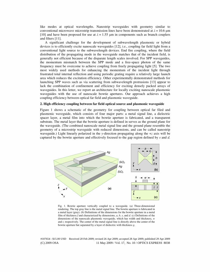
2. High efficiency coupling between far field optical source and plasmonic waveguide
Figure 1 shows a schematic of the geometry for coupling between optical far filed and
plasmonic waveguide, which consists of four major parts: a metal signal line, a dielectric
spacer layer, a metal film into which the bowtie aperture is fabricated, and a transparent
substrate. The metal layer that the bowtie aperture is defined in serves as the ground plane for
the waveguide. (The combined nanoscale metal signal line and the ground plane resemble the
geometry of a microstrip waveguide with reduced dimensions, and can be called nanostrip
waveguide.) Light linearly polarized in the y-direction propagating along the +z axis will be
captured by the bowtie aperture and effectively focused to the gap region defined by s and d.
y
x
z
Ag
SiO2
SiO2
Ag
(a)
x
z
w
t
g
f
(c)
x
y
a
b
s
d
(b)
Fig. 1. Bowtie aperture vertically coupled to a waveguide. (a) Three-dimensional
rendering. The top gray line is the metal signal line. The bowtie aperture is fabricated in
a metal layer (gray). (b) Definitions of the dimensions for the bowtie aperture in a metal
film of thickness f and characterized by dimensions, a, b, s, and d. (c) Definitions of the
dimensions of the nanoscale plasmonic waveguide, which has width and thickness, w
and t, respectively. The center of the metal signal line is directly above the center of the
bowtie aperture but separated by a layer of dielectric with thickness g.
(C) 2009 OSA 11 May 2009 / Vol. 17, No. 10 / OPTICS EXPRESS 8038#107654 - $15.00 USD Received 20 Feb 2009; revised 26 Apr 2009; accepted 28 Apr 2009; published 29 Apr 2009
(The reason for using a finite gap width s is due to the consideration of fabrication feasibility.)
With the proper selection of dimensions, the field emerging in the dielectric spacer layer will
efficiently couple to the plasmonic waveguide.
The principal advantage of this geometry is the ability to locally excite waveguides with
high efficiency. This is made possible by the bowtie aperture, which is a type of ridge
waveguide [8-9,14].
Ridge waveguide apertures (which can be considered as a short
waveguide), including shapes other than the bowtie such as ‘C’ and ‘H’ have been studied in
both the microwave regime and optical frequencies [15-18]. A key advantage of the bowtie
aperture is that the cutoff frequency is much lower than a regularly shaped aperture (i.e.
circular) with similar field confinement, which leads to dramatically higher transmission [15-
18]. At resonance the bowtie aperture effectively receives radiation over a large area and
focuses it to the gap region. This provides a high coupling efficiency with the waveguide. An
additional advantage of the coupling shown in Fig. 1 is that the antenna geometry is planner
and the coupling direction is vertical to the device plane, therefore multiple bowtie apertures
can made in parallel for parallel light coupling, modulation, and signal processing. Field
concentration and enhancement in bowtie apertures has been experimentally demonstrated,
including Near-Field Scanning Microscopy (NSOM or SNOM) measurements [19]. Bowtie
apertures have also been used to provide concentrated light sources for data storage [20] and
nanolithography [21-22], and as high efficiency light collectors for high resolution imaging
[23].
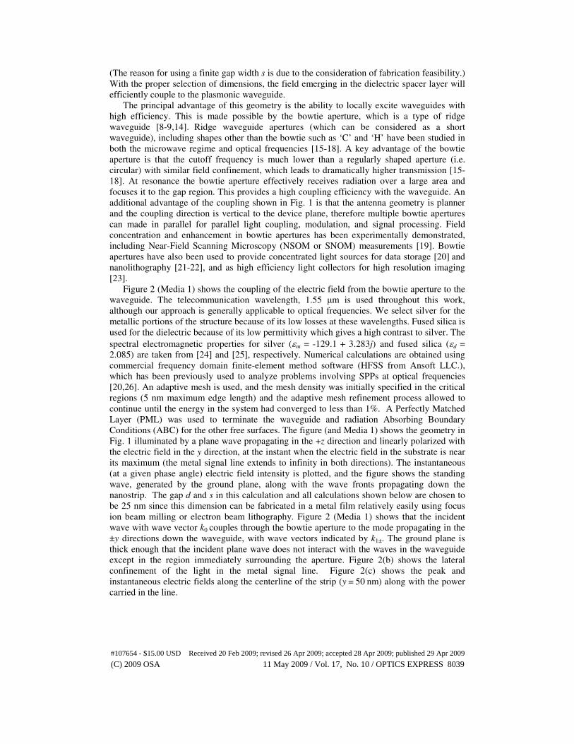
Figure 2 (Media 1) shows the coupling of the electric field from the bowtie aperture to the
waveguide. The telecommunication wavelength, 1.55 µm is used throughout this work,
although our approach is generally applicable to optical frequencies. We select silver for the
metallic portions of the structure because of its low losses at these wavelengths. Fused silica is
used for the dielectric because of its low permittivity which gives a high contrast to silver. The
spectral electromagnetic properties for silver (εm = -129.1 + 3.283j) and fused silica (εd =
2.085) are taken from [24] and [25], respectively. Numerical calculations are obtained using
commercial frequency domain finite-element method software (HFSS from Ansoft LLC.),
which has been previously used to analyze problems involving SPPs at optical frequencies
[20,26]. An adaptive mesh is used, and the mesh density was initially specified in the critical
regions (5 nm maximum edge length) and the adaptive mesh refinement process allowed to
continue until the energy in the system had converged to less than 1%. A Perfectly Matched
Layer (PML) was used to terminate the waveguide and radiation Absorbing Boundary
Conditions (ABC) for the other free surfaces. The figure (and Media 1) shows the geometry in
Fig. 1 illuminated by a plane wave propagating in the +z direction and linearly polarized with
the electric field in the y direction, at the instant when the electric field in the substrate is near
its maximum (the metal signal line extends to infinity in both directions). The instantaneous
(at a given phase angle) electric field intensity is plotted, and the figure shows the standing
wave, generated by the ground plane, along with the wave fronts propagating down the
nanostrip. The gap d and s in this calculation and all calculations shown below are chosen to
be 25 nm since this dimension can be fabricated in a metal film relatively easily using focus
ion beam milling or electron beam lithography. Figure 2 (Media 1) shows that the incident
wave with wave vector k0 couples through the bowtie aperture to the mode propagating in the
±y directions down the waveguide, with wave vectors indicated by k1±. The ground plane is
thick enough that the incident plane wave does not interact with the waves in the waveguide
except in the region immediately surrounding the aperture. Figure 2(b) shows the lateral
confinement of the light in the metal signal line. Figure 2(c) shows the peak and
instantaneous electric fields along the centerline of the strip (y = 50 nm) along with the power
carried in the line.
(C) 2009 OSA 11 May 2009 / Vol. 17, No. 10 / OPTICS EXPRESS 8039#107654 - $15.00 USD Received 20 Feb 2009; revised 26 Apr 2009; accepted 28 Apr 2009; published 29 Apr 2009
0
1
2
3
4
-3
-2
-1
0
1
2
3
0 1 2 3 4
PeakInstantaneous
Power
Ele
ctr
ic F
ield
[V
/m]
Po
wer in
nan
ostrip
[W×
10
16]
y [µm]
Fig. 2. Instantaneous electric field distribution showing coupling between a plane wave and the
waveguide. A y-polarized plane wave incident on a 250 nm bowtie aperture (25 nm gap)
coupling to a 100 wide transmission line separated from the bowtie aperture by a gap of 100
nm. The magnitudes of the electric fields are plotted: (a) (Media 1) yz plane through the centre
of the aperture with inset showing xz plane. The black arrow of the incident wave vector points
to the center of the bowtie aperture. (b) xy plane midway through the dielectric region (z = 50
nm). The magnitude of the incident electric field is 1 V/m in the fused silica substrate. In the
figures, the field is saturated at 2.5 V/m for clarity. A movie of light propagation from far field
into the waveguide is provided in supplementary information. (c) Peak and instantaneous
values of the electric field along the centerline of the nanostrip (z = 50 nm) and the power
carried in the line as a function of distance from the center of the aperture.
y
z
(b) z = 50 nm a = b = 250 nm
s = d = 25 nm
f = 100 nm
w = 100 nm
g = 100 nm
|E| [V/m]
0.0 0.5 1.0 1.5 2.0 2.5
y
x
(a)
k0 �
k1+
� k1- �
x = 0
x
z y = 0
(C) 2009 OSA 11 May 2009 / Vol. 17, No. 10 / OPTICS EXPRESS 8040#107654 - $15.00 USD Received 20 Feb 2009; revised 26 Apr 2009; accepted 28 Apr 2009; published 29 Apr 2009
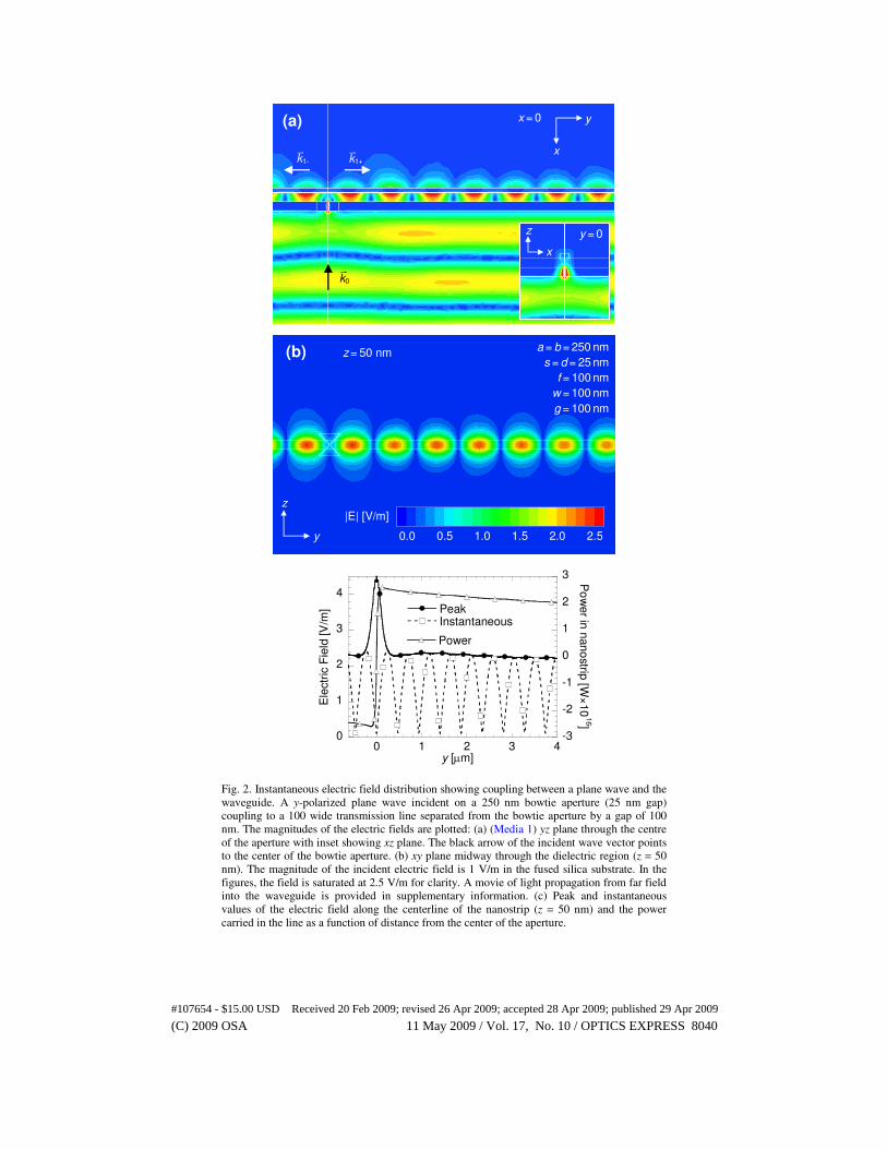
In the waveguide, light is attenuated as it propagates along the waveguide due to metal
losses. After an initial transition length (less than 0.5 µm from the center of the aperture), the
field decays exponentially. The power carried by the waveguide at a given point y can be
obtained by integrating the y component of the Poynting vector over the xz plane through that
point. The coupling efficiency from a far field light source to the waveguide is computed as
the ratio between the equivalent initial power in the waveguide directly above the bowtie
aperture and the power incident on the bowtie aperture within a diffraction limited spot at the
1.55 µm wavelength (945.5 nm diameter). This equivalent initial power is obtained by fitting
the exponential decay function to the power in the waveguide outside the transition length (y >
0.5 µm) and extrapolating back to y = 0. The power in the waveguide is equally divided
between the two branches (traveling in the ±y directions). Figure 3 shows how this coupling
efficiency varies with geometry parameters. More than 30% of the power within a diffraction
limited spot can be coupled into the waveguides (including power traveling in both directions
of the waveguide). It should be noted that techniques such as oil immersion lenses can be used
to reduce the diffraction–limited spot size, which will increase the coupling efficiency defined
here. On the other hand, if the open area of the bowtie aperture is used to compute the total
incident power, the efficiencies shown in Fig. 3 will increase by a factor of 22, making the
highest efficiency greater than 660%. That is, a properly dimensioned bowtie aperture couples
as much as six times of the radiation on its opening area into the waveguide. It is important to
note that these results are only for light polarized in the y-direction. The coupling to the
aperture is very sensitive to polarization and if the light is polarized in the x-direction, the
coupling to the nanostrip aperture is negligible.
0
0.05
0.1
0.15
0.2
0.25
0.3
0.35
0 25 50 75 100 125 150 175 200
250/50250/100250/150200/100300/100
Po
we
r co
uplin
g c
oeff
icie
nt
g [nm]
a / w [nm]
Fig. 3. Coupling efficiency from a far field light source to the waveguide. The far field light
source is assumed to be a diffraction limited spot incident on the bowtie aperture with a
diameter of 945.5 nm. For the bowtie aperture, a = b is used. s = d = 25 nm, f = 100 nm, and t =
50 nm.
The dependence of the coupling efficiency on the geometric parameters can be seen from
Fig. 3. The outline dimensions of the aperture, a and b (a = b is used), dramatically affect the
coupling efficiency. This is due to the resonance of the aperture which is to be discussed in
more detail later. For the off-resonance apertures (a = 200 and 300 nm), increasing the gap
decreases the coupling efficiency. For the resonant aperture (a = 250 nm), there is an optimum
gap g which varies with the width of the waveguide. Other parameters have a lesser effect on
the coupling efficiency. In order to obtain a better understanding of how various parameters
affect the coupling efficiency, we provide analyses below of the individual components,
starting with the light propagation along the waveguide and then the transmission and
resonance of the bowtie aperture.
(C) 2009 OSA 11 May 2009 / Vol. 17, No. 10 / OPTICS EXPRESS 8041#107654 - $15.00 USD Received 20 Feb 2009; revised 26 Apr 2009; accepted 28 Apr 2009; published 29 Apr 2009
3. Detailed analysis of coupling of EM field between the plasmonic waveguide and the
bowtie aperture
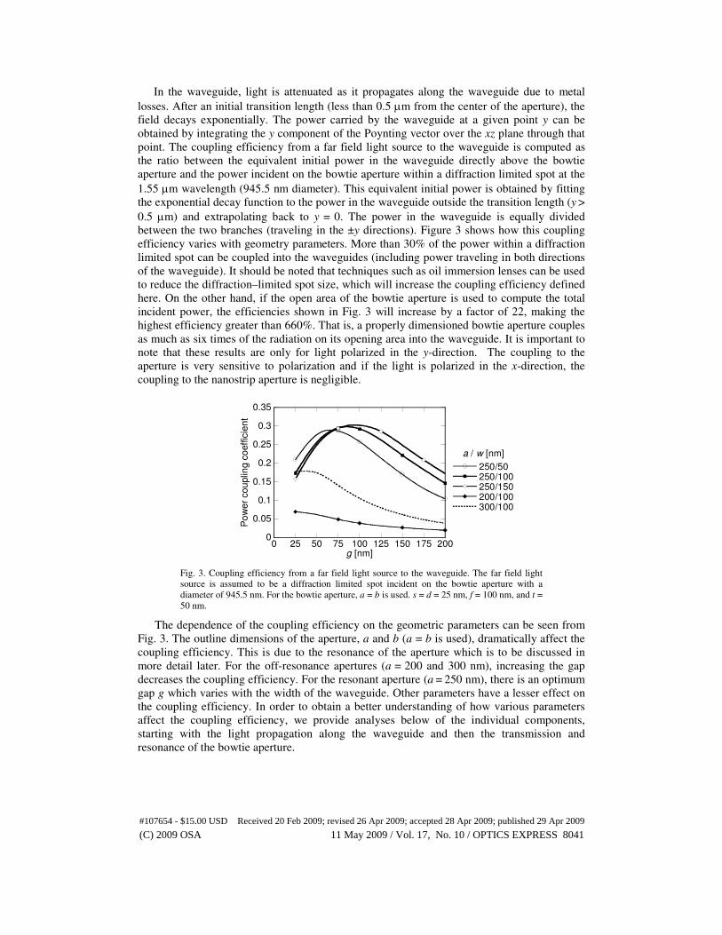
The field distribution in the waveguide past the transition region (~ 0.5µm or less) can be
obtained from its eigenmode solution [26]. The power and field distributions in the waveguide
are plotted in Fig. 4(a). This is a hybrid mode resembling the quasi-TEM field distribution for
a conventional microstrip albeit with significant field penetration into the metal films. There
are longitudinal electric and magnetic components but their magnitudes are two orders of
magnitude lower than those of the transverse components. The figure shows that the field is
well confined within the waveguide with the majority of the power carried in the dielectric
layer and very high intensities at the corners. The mode area, Am, is a metric of the field
confinement and is defined as the ratio of the total power carried through a cross-section of
the waveguide to the peak intensity in the same cross-section:
{ }
{ }
*
*
max
Re
Re
A
m
dAA
×=
×
∫∫ E H
E H (1)
0
5
10
15
20
0 50 100 150 200
50100150200
Am [
nm
2]
g [nm]
w [nm]
x103
Fig. 4. Properties of the nanostrip waveguide. (a) Magnitude of the Poynting vector along the
waveguide with the size of w = 200 nm, g = 100 nm and t = 50 nm. Solid field lines show the
direction of the electric field and dashed indicate the direction of the magnetic field. The
waveguide is transmitting 1 nW total power. The intensity is saturated at 50 kW/m2 for clarity.
(b) Mode area, defined as the ratio of the total power carried in the transmission line divided by
the peak power intensity. (c) Propagation length for different geometries. (d) Ratio between the
peak intensity in the waveguide at 4 µm away from the center (y = 4 µm) and the incident
intensity.
(b)
0
5
10
15
20
0 50 100 150 200
250/50250/100250/150200/100300/100
Inte
nis
ty c
ouplin
g c
oeff
icie
nt
g [nm]
a / w [nm]y = 4 µm
(d)
εm
εd
ε0 εm
(a)
x
z
-0.50 16.3 33.2 50.0
Sy [kW/m2]
5
10
15
20
25
30
35
0 50 100 150 200
50100150200
Lm [µ
m]
g [nm]
w [nm]
(c)
(C) 2009 OSA 11 May 2009 / Vol. 17, No. 10 / OPTICS EXPRESS 8042#107654 - $15.00 USD Received 20 Feb 2009; revised 26 Apr 2009; accepted 28 Apr 2009; published 29 Apr 2009
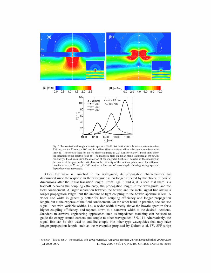
The sharp corners on the metal signal line lead to a very high field. The maximum
intensity used in Eq. (1) is the intensity averaged over a 4 nm diameter circle centered about
the corners. This underestimates the peak intensity; however, it allows a finite radius which
would result from any practical fabrication method. The mode area vs. waveguide geometry is
shown in Fig. 4(b), which shows that a waveguide defined by w = g = 100 nm and t = 50 nm
has a field confinement better than λ2/250. Also, it can be seen that the mode area is roughly
proportionate to cross sectional area of the waveguide. Figure 4(c) shows how the propagation
lengths in the waveguide are affected by the waveguide dimensions, which is defined as the
distance at which the power diminishes to 1/e of its original value, and is equal to
{ }1 2 ImmL k= (2)
where k is the complex propagation constant. Generally it can be seen that the propagation
length is longer for the larger separations and wider metal signal lines. This can be attributed
to more of the power being carried in the dielectric as opposed to the metal portions of the
waveguide.
The peak field intensities in the waveguide are significantly higher than that of the
incident plane wave and are confined along the edges of the metal signal line. The peak
intensity (4 µm from the aperture) can be nearly 20 times of that of the incident wave as
shown in Fig. 4(d). The tight field confinement and high peak intensity are particularly useful
for applications such as molecular sensing.
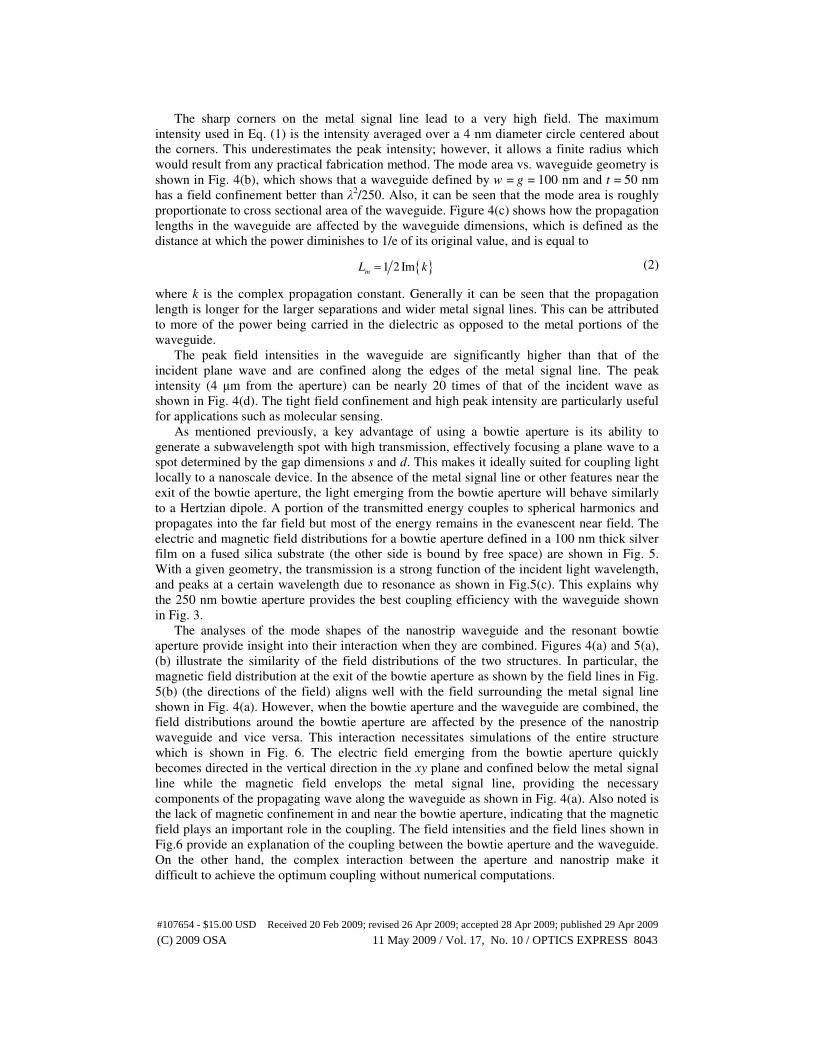
As mentioned previously, a key advantage of using a bowtie aperture is its ability to
generate a subwavelength spot with high transmission, effectively focusing a plane wave to a
spot determined by the gap dimensions s and d. This makes it ideally suited for coupling light
locally to a nanoscale device. In the absence of the metal signal line or other features near the
exit of the bowtie aperture, the light emerging from the bowtie aperture will behave similarly
to a Hertzian dipole. A portion of the transmitted energy couples to spherical harmonics and
propagates into the far field but most of the energy remains in the evanescent near field. The
electric and magnetic field distributions for a bowtie aperture defined in a 100 nm thick silver
film on a fused silica substrate (the other side is bound by free space) are shown in Fig. 5.
With a given geometry, the transmission is a strong function of the incident light wavelength,
and peaks at a certain wavelength due to resonance as shown in Fig.5(c). This explains why
the 250 nm bowtie aperture provides the best coupling efficiency with the waveguide shown
in Fig. 3.
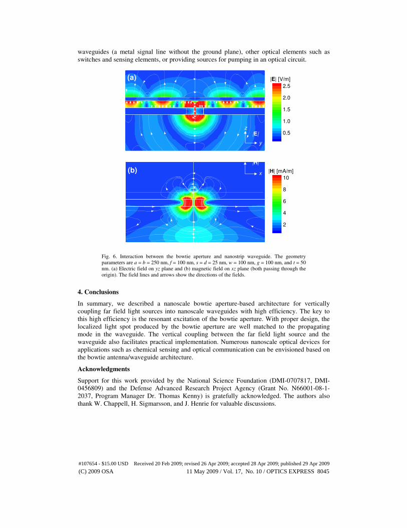
The analyses of the mode shapes of the nanostrip waveguide and the resonant bowtie
aperture provide insight into their interaction when they are combined. Figures 4(a) and 5(a),
(b) illustrate the similarity of the field distributions of the two structures. In particular, the
magnetic field distribution at the exit of the bowtie aperture as shown by the field lines in Fig.
5(b) (the directions of the field) aligns well with the field surrounding the metal signal line
shown in Fig. 4(a). However, when the bowtie aperture and the waveguide are combined, the
field distributions around the bowtie aperture are affected by the presence of the nanostrip
waveguide and vice versa. This interaction necessitates simulations of the entire structure
which is shown in Fig. 6. The electric field emerging from the bowtie aperture quickly
becomes directed in the vertical direction in the xy plane and confined below the metal signal
line while the magnetic field envelops the metal signal line, providing the necessary
components of the propagating wave along the waveguide as shown in Fig. 4(a). Also noted is
the lack of magnetic confinement in and near the bowtie aperture, indicating that the magnetic field plays an important role in the coupling. The field intensities and the field lines shown in
Fig.6 provide an explanation of the coupling between the bowtie aperture and the waveguide.
On the other hand, the complex interaction between the aperture and nanostrip make it
difficult to achieve the optimum coupling without numerical computations.
(C) 2009 OSA 11 May 2009 / Vol. 17, No. 10 / OPTICS EXPRESS 8043#107654 - $15.00 USD Received 20 Feb 2009; revised 26 Apr 2009; accepted 28 Apr 2009; published 29 Apr 2009
0
20
40
60
80
100
120
1000 1200 1400 1600 1800
200250300
|S| /
S0
λ0 [nm]
a = b [nm] s = d = 25 nm
f = 100 nm
Fig. 5. Transmission through a bowtie aperture. Field distribution for a bowtie aperture (a = b =
250 nm, s = d = 25 nm, t = 100 nm) in a silver film on a fused silica substrate at one instant in
time. (a) The electric field on the yz plane (saturated at 2.5 V/m for clarity). Field lines show
the direction of the electric field. (b) The magnetic field on the xz plane (saturated at 10 mA/m
for clarity). Field lines show the direction of the magnetic field. (c) The ratio of the intensity at
the centre of the gap on the exit plane to the intensity of the incident plane wave for different
bowties (s = d = 25 nm, f = 100 nm) as a function of wavelength, showing strong spectral
dependence and resonance.
Once the wave is launched in the waveguide, its propagation characteristics are
determined since the response in the waveguide is no longer affected by the choice of bowtie
dimensions after the initial transition length. From Figs. 3 and 4, it is seen that there is a
tradeoff between the coupling efficiency, the propagation length in the waveguide, and the
field confinement. A larger separation between the bowtie and the metal signal line allows a
longer propagation length, but the amount of light coupling to the bowtie aperture is less. A
wider line width is generally better for both coupling efficiency and longer propagation
length, but at the expense of the field confinement. On the other hand, in practice, one can use
signal lines with variable widths, i.e., a wider width directly above the bowtie aperture for a
higher coupling efficiency, and tapered down to a narrower width at the desired locations.
Standard microwave engineering approaches such as impedance matching can be used to
guide the energy around corners and couple to other waveguides [8-9, 11]. Alternatively, the
signal line can be also used to end-fire couple into other type waveguides that may have
longer propagation length, such as the waveguide proposed by Oulton et al. [7], SPP stripe
(a)
ε0
εd
εm
0.0 0.5 1.0 1.5 2.0 2.5
|E| [V/m]
0.0 2.0 4.0 6.0 8.0 10.0
|H| [mA/m]
(b)
(C) 2009 OSA 11 May 2009 / Vol. 17, No. 10 / OPTICS EXPRESS 8044#107654 - $15.00 USD Received 20 Feb 2009; revised 26 Apr 2009; accepted 28 Apr 2009; published 29 Apr 2009
waveguides (a metal signal line without the ground plane), other optical elements such as
switches and sensing elements, or providing sources for pumping in an optical circuit.
Fig. 6. Interaction between the bowtie aperture and nanostrip waveguide. The geometry
parameters are a = b = 250 nm, f = 100 nm, s = d = 25 nm, w = 100 nm, g = 100 nm, and t = 50
nm. (a) Electric field on yz plane and (b) magnetic field on xz plane (both passing through the
origin). The field lines and arrows show the directions of the fields.
4. Conclusions
In summary, we described a nanoscale bowtie aperture-based architecture for vertically
coupling far field light sources into nanoscale waveguides with high efficiency. The key to
this high efficiency is the resonant excitation of the bowtie aperture. With proper design, the
localized light spot produced by the bowtie aperture are well matched to the propagating
mode in the waveguide. The vertical coupling between the far field light source and the
waveguide also facilitates practical implementation. Numerous nanoscale optical devices for
applications such as chemical sensing and optical communication can be envisioned based on
the bowtie antenna/waveguide architecture.
Acknowledgments
Support for this work provided by the National Science Foundation (DMI-0707817, DMI-
0456809) and the Defense Advanced Research Project Agency (Grant No. N66001-08-1-
2037, Program Manager Dr. Thomas Kenny) is gratefully acknowledged. The authors also
thank W. Chappell, H. Sigmarsson, and J. Henrie for valuable discussions.
(a)
|E|
y
z
(b) x
z |H|
2.5
2.0
1.5
1.0
0.5
|E| [V/m]
|H| [mA/m]
10
8
6
4
2
(C) 2009 OSA 11 May 2009 / Vol. 17, No. 10 / OPTICS EXPRESS 8045#107654 - $15.00 USD Received 20 Feb 2009; revised 26 Apr 2009; accepted 28 Apr 2009; published 29 Apr 2009