Embed Size (px)
Citation preview

March 2004 • NREL/SR-560-35059
M.S. Illindala, P. Piagi, H. Zhang, G. Venkataramanan, R.H. Lasseter Wisconsin Power Electronics Research Center Madison, Wisconsin
Hardware Development of a Laboratory-Scale Microgrid Phase 2: Operation and Control of a Two-Inverter Microgrid
National Renewable Energy Laboratory 1617 Cole Boulevard Golden, Colorado 80401-3393 NREL is a U.S. Department of Energy Laboratory Operated by Midwest Research Institute • Battelle
Contract No. DE-AC36-99-GO10337
March 2004 • NREL/SR-560-35059
Hardware Development of a Laboratory-Scale Microgrid Phase 2: Operation and Control of a Two-Inverter Microgrid
M.S. Illindala, P. Piagi, H. Zhang, G. Venkataramanan, R.H. Lasseter Wisconsin Power Electronics Research Center Madison, Wisconsin
NREL Technical Monitor: Holly Thomas Prepared under Subcontract No. AAD-0-30605-14
National Renewable Energy Laboratory 1617 Cole Boulevard Golden, Colorado 80401-3393 NREL is a U.S. Department of Energy Laboratory Operated by Midwest Research Institute • Battelle
Contract No. DE-AC36-99-GO10337

NOTICE This report was prepared as an account of work sponsored by an agency of the United States government. Neither the United States government nor any agency thereof, nor any of their employees, makes any warranty, express or implied, or assumes any legal liability or responsibility for the accuracy, completeness, or usefulness of any information, apparatus, product, or process disclosed, or represents that its use would not infringe privately owned rights. Reference herein to any specific commercial product, process, or service by trade name, trademark, manufacturer, or otherwise does not necessarily constitute or imply its endorsement, recommendation, or favoring by the United States government or any agency thereof. The views and opinions of authors expressed herein do not necessarily state or reflect those of the United States government or any agency thereof.
Available electronically at http://www.osti.gov/bridge
Available for a processing fee to U.S. Department of Energy and its contractors, in paper, from:
U.S. Department of Energy Office of Scientific and Technical Information P.O. Box 62 Oak Ridge, TN 37831-0062 phone: 865.576.8401 fax: 865.576.5728 email: [email protected]
Available for sale to the public, in paper, from:
U.S. Department of Commerce National Technical Information Service 5285 Port Royal Road Springfield, VA 22161 phone: 800.553.6847 fax: 703.605.6900 email: [email protected] online ordering: http://www.ntis.gov/ordering.htm
Printed on paper containing at least 50% wastepaper, including 20% postconsumer waste

iii
Executive Summary The evolution of the technology sector has made equipment sensitive to power-quality events such as voltage sags, voltage imbalances, and harmonics more common. These sensitive loads include critical computing equipment, data processing electronic equipment, and semiconductor fabrication machinery. Such sensitive loads demand a highly reliable power supply for fail-safe operation, and downtime caused by power-quality events has resulted in significant loss of revenue. Conventional approaches to solving these problems use uninterruptible power supply (UPS) systems. Emerging, efficient electrical generation systems such as fuel cells, microturbines, variable-speed wind turbines, and photovoltaic arrays—generally called distributed resources (DR)—can be placed in proximity to loads. Some of these sources also enable simultaneous harvest of heat byproduct. DR invariably incorporate power electronic converters along with small amounts of energy storage and are capable of providing UPS functionality, power quality improvement, and energy conversion simultaneously at a reasonable cost. However, their operational and control features must be upgraded to enable them to become solutions to the sensitive load problem. The major thrust of this project is to develop and demonstrate operational and control features of inverter-embedded DR to enable them to operate in conjunction with the conventional electric grid in a safe, stable, and reliable manner that is satisfactory for premium-power applications and has no negative effect on grid power quality. As the central project activity, essential generation control features that enable real and reactive power sharing for parallel operation were developed. They permit rapid synchronization to the grid and disconnection. They also enable the operation of inverter-embedded DR in a manner similar to that of conventional rotating machine-based systems. Furthermore, capabilities for regulating the terminal voltage of sensitive load equipment under power-quality phenomena such as voltage imbalances, voltage sags, and harmonics have been incorporated into the system controller. Conventional systems, in contrast, typically disconnect from the system under such conditions. These operational concepts have been developed using detailed analytical models developed under the project and verified with extensive computer simulations also developed under the project. After refinement the models and control concepts, they are demonstrated on a laboratory-scale microgrid that incorporates emulated DR sources. During Phase 2, the laboratory-scale microgrid was expanded to include:
• Two emulated DR sources • Static switchgear to allow rapid disconnection and reconnection • Electronic synchronizing circuitry to enable transient-free grid interconnection • Control software for dynamically varying the frequency and voltage controller structures • Power measurement instrumentation for capturing transient waveforms at the
interconnect during switching events.

iv
All of these devices have been tested extensively and found to operate reliably to the extent that they have allowed the capture of detailed dynamic phenomena valuable in refining control concepts. Interconnection dynamics between one DR source and the electric grid are being tested regularly, and several key control concepts have been verified and refined. The gain and dynamics of frequency and voltage controllers have been found to be key parameters that affect the strength of the interconnection. During Phase 3 of the project, the laboratory-scale microgrid will be expanded to include a third emulated DR source and digital protective relays. The expansion will allow the characterization of interconnection transients during switching events among multiple combinations of DR sources and the grid. The analytical and computer simulation models will be extended to study the dynamic operation of an arbitrary number of DR sources in a microgrid. Based on the analytical models and the test results, guidelines for structuring the frequency and voltage control loops will be developed. Operation of the controller under power-quality disturbances such as imbalances, voltage sags, and voltage swells will be verified. Continuation and completion of the work is considered critical to the successful demonstration of trouble-free operation under abnormal operating conditions so that the availability of DR during contingencies may be guaranteed.

v
Table of Contents 1 Project Overview ...........................................................................................................................1
1.1 Sensitive Loads .......................................................................................................... 1 1.2 Distributed Generation ............................................................................................... 2 1.3 Development Scenarios for Distributed Generation .................................................. 4 1.4 Distributed Generation for Sensitive Loads............................................................... 4 1.5 Technical Challenges ................................................................................................. 5 1.6 Systems Approach...................................................................................................... 6 1.7 Hardware Test Bed..................................................................................................... 7 1.8 Report Organization ................................................................................................... 9
2 Microgrids With Power Quality Conditioning...........................................................................10
2.1 Power Quality Events............................................................................................... 10 2.2 Effects on Sensitive Loads ....................................................................................... 11 2.3 Power Quality Solutions .......................................................................................... 13 2.4 Microgrid ................................................................................................................. 13
2.4.1 Static Switch............................................................................................ 15 2.4.2 Static Switch/Contactor Controller ......................................................... 16
3 Microgrid: A Case Study ............................................................................................................18
3.1 Components of the Microgrid .................................................................................. 18 3.2 Modeling of Microgrid Components ....................................................................... 20
3.2.1 Transformers ........................................................................................... 20 3.2.2 Lines and Cables ..................................................................................... 22 3.2.3 Loads....................................................................................................... 33 3.2.4 Distributed Resources ............................................................................. 35
3.3 System Design and Modeling .................................................................................. 38 3.4 Principle of Operation of the Distributed Resources ............................................... 39
3.4.1 Controls for Grid-Interfaced Operation.................................................. 43 3.4.2 Controls for Island Operation................................................................. 44
3.5 Simulation Results ................................................................................................... 46 3.5.1 Island Mode of Operation....................................................................... 47 3.5.2 Grid-Interfaced Mode of Operation........................................................ 49
4 Operation and Control of a Distributed Resource Under Imbalance.....................................54
4.1 Complex Representation of Imbalanced Three-Phase Quantities............................ 56 4.2 Complex Transfer Functions.................................................................................... 59 4.3 Control Architecture ................................................................................................ 62
4.3.1 Filter Inductor Current Regulator ........................................................... 65 4.3.2 Filter Capacitor Voltage Regulator ........................................................ 67 4.3.3 Command Voltage Modifier................................................................... 71 4.3.4 Performance of the Voltage Regulator Against Imbalances .................. 77
vi
4.4 Three-Phase Voltage Reference Generation for the Distributed Resource.............. 83 4.5 Control of Real Power.............................................................................................. 85
4.5.1 Generation Control in a Two-Machine Interconnected Power System.. 86 4.5.2 Control of Real Power Flow in a Distributed UPS System/Microgrid .. 96
4.6 Control of Reactive Power in a Microgrid............................................................. 114 4.7 Grid-Interfaced Mode of Operation of the Microgrid............................................ 122
5 Distributed Resource Controller Experimental Implementation ..........................................125
5.1 Internal Voltage and Current Regulator Implementation....................................... 125 5.2 External Power Regulator Implementation............................................................ 127
6 Conclusions...............................................................................................................................136 7 References.................................................................................................................................138

vii
List of Figures Figure 1. Block diagram of microturbine power generation system ................................ 3 Figure 2. Block diagram of fuel cell power generation system........................................ 3 Figure 3. Block diagram of proposed model DR system ................................................. 6 Figure 4. Conceptual one-line schematic of the experimental test bed ............................ 7 Figure 5. ITI/CBEMA curves specifying acceptable voltage sensitivity levels............. 12 Figure 6. SEMI F47 voltage sag immunity curve .......................................................... 12 Figure 7. Simplified schematic of a microgrid consisting of two DR............................ 14 Figure 8. Power circuit schematic of the static switch ................................................... 15 Figure 9. Schematic of the static switch/contactor control circuit ................................. 16 Figure 10. Schematic of a microgrid for an office-cum-warehouse facility .................... 18 Figure 11. Schematic of the 120-kV tower....................................................................... 26 Figure 12. Schematic of the 13.8-kV pole........................................................................ 28 Figure 13. Geometrical disposition of buried cable ......................................................... 28 Figure 14. DR connection to a local feeder ...................................................................... 36 Figure 15. P&Q injected into the network spanning X .................................................... 37 Figure 16. P&Q injected into the network spanning δp .................................................... 38 Figure 17. Single-phase equivalent of the office-cum-warehouse facility....................... 39 Figure 18. Inverter switch topology ................................................................................. 40 Figure 19. Flux space vector positions and sector locations ............................................ 40 Figure 20. Pulse generator block ...................................................................................... 42 Figure 21. Detailed inverter control scheme .................................................................... 43 Figure 22. Power with frequency droop ........................................................................... 44 Figure 23. P-ω droop characteristic.................................................................................. 45 Figure 24. Real power across lines L1 and L2 for a step change in Load12 in
island mode ..................................................................................................... 47 Figure 25. Real power outputs of DR1 and DR2 for a step change in Load12 in
island mode...................................................................................................... 48 Figure 26. Reactive power outputs of DR1 and DR2 for a step change in Load12 in
island mode...................................................................................................... 48 Figure 27. Terminal voltages of DR1 and DR2 for a step change in Load12 in
island mode...................................................................................................... 49 Figure 28. Real power across lines L1 and L2 for a step change in Load12 in
grid-interfaced mode........................................................................................ 50 Figure 29. Real power outputs of DR1 and DR2 for a step change in Load12 in
grid-interfaced mode........................................................................................ 51 Figure 30. Reactive power outputs of DR1 and DR2 for a step change in Load12 in
grid-interfaced mode........................................................................................ 52 Figure 31. Terminal voltages of DR1 and DR2 for a step change in Load12 in
grid-interfaced mode........................................................................................ 52 Figure 32. Power circuit schematic of the three-phase inverter and its connection
to three-phase loads ......................................................................................... 55 Figure 33. Complex vector mapping of three-phase AC sinusoidal signals under
(a) balanced and (b) negative sequence imbalanced conditions...................... 58 Figure 34. Fourier amplitude spectra of (a) cos(ω60t) and (b) sin(ω60t)............................ 59

viii
Figure 35. Characteristics of real low-pass filter Grlpf(s) ................................................. 60 Figure 36. Characteristics of complex filter Gcbpf(s)........................................................ 61 Figure 37. Bode plot of the complex band-pass filter Gcbpf(s) for (a) positive and
(b) negative sequence components of the complex space vector ................... 62 Figure 38. Block diagram of the power circuit of the filter-interface network................ 64 Figure 39. Block diagram of the control architecture for the DR inverter system........... 64 Figure 40. Block diagram of the current regulator of the DR inverter system ................ 65 Figure 41. Bode plot of the loop gain for the current regulator loop for (a) positive
and (b) negative sequence components of the space vector ........................... 66 Figure 42. Block diagram illustrating the realization of complex voltage controller
transfer function Gcvp(s).................................................................................. 68 Figure 43. Bode plot of the loop gain for the voltage regulator loop for (a) positive
and (b) negative sequence components of the space vector ........................... 69 Figure 44. Bode plot of the transfer function Go(s) (a) without the multi-loop
controller and (b) with the multi-loop controller............................................ 71 Figure 45. Block diagram of the command voltage modifier .......................................... 72 Figure 46. Block diagram illustrating realization of PSF in the command voltage
modifier .......................................................................................................... 73 Figure 47. Block diagram illustrating realization of complex gain jω60 Lt for the
output of the PSF in Clarke’s αβ coordinates ................................................ 74 Figure 48. Bode plot of the open-loop gain for the PSF for positive and negative
sequence components of the space vector iLt(t) .............................................. 74 Figure 49. Block diagram illustrating realization of NSF in the command voltage
modifier .......................................................................................................... 76 Figure 50. Block diagram illustrating realization of -jω60 Lt for the NSF in Clarke’s
αβ coordinates ................................................................................................ 76 Figure 51. Bode plot of the open-loop gain for the NSF for positive and negative
sequence components of the space vector iLt(t) .............................................. 77 Figure 52. Effect of imbalance (left) on the unregulated terminal voltage (right)........... 78 Figure 53. Operation of the current control loop for iLf(t) ............................................... 79 Figure 54. Operation of the voltage control loop for vCf(t).............................................. 80 Figure 55. Line voltages at the load bus vxnL(t) - vbnL(t) (x = a, c), illustrating that it
does not contain negative sequence imbalance .............................................. 81 Figure 56. Performance of the PSF on the reactor current iLt(t) ...................................... 82 Figure 57. Performance of the NSF on the reactor current iLt(t)...................................... 83 Figure 58. Block diagram for determining the voltage reference vload*(t)....................... 85 Figure 59. Block diagram of generation controller for a rotating machine ..................... 87 Figure 60. Steady-state frequency droop of the generator ............................................... 88 Figure 61. Single-line diagram of real power flow of an interconnected power system
consisting of two generators ........................................................................... 89 Figure 62. Block diagram of the governor control for an interconnected power
system consisting of two generators ............................................................... 91 Figure 63. Response of the interconnected power system to a load change of
∆PL1=0.2 pu .................................................................................................... 93 Figure 64. Sharing of the load change between the two generators in the
interconnected power system.......................................................................... 96

ix
Figure 65. Frequency-droop curves of the interconnected power system ....................... 96 Figure 66. UPS/DR with voltage regulation analogy to a voltage source for
power studies .................................................................................................. 97 Figure 67. Block diagram of Chandorkar’s real power-frequency controller for a
distributed UPS............................................................................................... 98 Figure 68. Frequency droop showing deviation quantities of the generator.................... 99 Figure 69. Frequency droop showing actual quantities of the generator ....................... 100 Figure 70. Single-line diagram illustrating real power flow of a distributed UPS
consisting of two UPSs................................................................................. 100 Figure 71. Block diagram of the governor control for an interconnected distributed
UPS system consisting of two UPSs ............................................................ 101 Figure 72. Response of the distributed UPS system to a load change of
∆PL1 = 0.2 pu................................................................................................. 104 Figure 73. Sharing of the load change between the two UPSs in the interconnected
power system ................................................................................................ 105 Figure 74. Frequency-droop curves of the interconnected power system ..................... 106 Figure 75. Single distributed UPS unit .......................................................................... 108 Figure 76. Block diagram of Chandorkar’s real power-frequency controller for
a DR.............................................................................................................. 108 Figure 77. Single-line diagram illustrating real power flow of a microgrid consisting
of two DR ..................................................................................................... 109 Figure 78. Block diagram of the frequency droop and governor control for a
microgrid consisting of two DR ................................................................... 110 Figure 79. Response of the microgrid to (a) load change of ∆PL1 = 0.2 pu and
(b) load reference setpoint change of ∆PL1-ref = 0.2 pu ................................. 111 Figure 80. Sharing of load change between the two units in the interconnected
system ........................................................................................................... 112 Figure 81. Frequency-droop curves of the interconnected power system ..................... 114 Figure 82. Block diagram of the proposed reactive power controller for a DR............. 115 Figure 83. Steady-state voltage droop of the DR........................................................... 116 Figure 84. Single-line diagram illustrating reactive power flow of a microgrid
consisting of two DR .................................................................................... 117 Figure 85. Block diagram of the reactive power control of a DR consisting of
two DR.......................................................................................................... 119 Figure 86. Response of the microgrid to a load change of ∆QL1=0.2 pu ....................... 121 Figure 87. Steady-state frequency and voltage droop characteristics of the
grid supply .................................................................................................... 123 Figure 88. Sharing of the load change between the microgrid and the grid supply
while operating in the grid-interfaced mode................................................. 123 Figure 89. Waveforms showing DC offsets in the measurements of AC quantities ..... 126 Figure 90. Waveforms showing instability of the controller because of large
sampling delay .............................................................................................. 127 Figure 91. Phase A currents in different branches at the load bus during transition
from standalone to grid-interfaced mode of operation ................................. 128 Figure 92. Phase A currents in different branches at the load bus during transition
from standalone to grid-interfaced mode of operation (zoomed version) .... 129

x
Figure 93. Phase A currents in different branches at the load bus during the standalone mode of operation....................................................................... 130
Figure 94. Phase A currents in different branches at the load bus in the grid-interfaced mode of operation demonstrating quasi-periodic behavior of oscillations................................................................................. 131
Figure 95. Phase A currents in different branches at the load bus during the grid-interfaced mode of operation demonstrating quasi-periodic behavior of oscillations (zoomed version).................................................... 132
Figure 96. Phase A currents in different branches at the load bus during the grid-interfaced mode of operation (magnified version)................................ 133
Figure 97. Transition from standalone to grid-interfaced mode of operation................ 134 Figure 98. Transition from standalone to grid-interfaced mode of operation
(zoomed version) .......................................................................................... 135

xi
List of Tables Table 1. Transformer Summary for Microgrid Case Study .......................................... 19 Table 2. Load Summary for Microgrid Case Study ...................................................... 19 Table 3. Cable Summary for Microgrid Case Study..................................................... 20 Table 4. Cables in Building........................................................................................... 22 Table 5. Current Capabilities: Aerial Cable .................................................................. 23 Table 6. Current Capabilities: Raceway and Buried ..................................................... 24 Table 7. Sequence Parameters of Cables ...................................................................... 25 Table 8. Choice of the Switching Vector ...................................................................... 41 Table 9. Circuit Parameters of the DR .......................................................................... 55
1
1 Project Overview This project is focused on a systems approach to using clusters of microsources with storage to bring high value to electrical energy customers. Advantages of such an approach include deferred distribution cost, local voltage control and reliability, coordinated demand-side management, and premium power quality. This project addresses the control and placement of distributed resources (DR) as a solution to the sensitive-load problem. In particular, the focus is on systems of DR that can switch from grid connection to island operation without causing any disturbance to critical loads. The presence of power electronic interfaces in fuel cells, photovoltaics, wind turbines, microturbines, and storage technologies creates a very different situation from more conventional synchronous generator and induction-based sources in power sources and standby emergency power systems. This project takes advantage of the properties of the power electronic interface to provide functionality to distributed generators beyond the supply of electrical energy. The approaches are verified using computer simulation models, and their feasibility is established on a hardware test bed. The hardware demonstration component is based on a three-phase, 480-V distribution test bed with emulated microsources and storage, passive loads, induction machines, and adjustable-speed drives. This report describes activities from the second phase of the project. 1.1 Sensitive Loads In recent years, various industries have installed precision equipment such as robots, automated machine tools, and materials-processing equipment to realize increased product quality and productivity. As a result, modern industrial facilities have come to depend on sensitive electronic equipment that can be shut down suddenly by power system disturbances. Although voltage spikes, harmonics, and grounding-related problems may cause such problems, they can be overcome through appropriate design of robustness into control circuits. A majority of problems occur because processes are not able to maintain precision control because of a power outage that lasts a single cycle or voltage sags that last more than two cycles. A few cycles of disturbance in voltage waveform may cause a motor to slow down and draw additional reactive power. This depresses the voltage even deeper and eventually leads to a process shutdown. This results in equipment malfunction and high restart cost. The number of outages and voltages dips and their durations are an important issue. In the manufacture of computer chips alone, losses from sags amount to $1 million to $4 million per occurrence, according to Central Hudson Gas and Electrical Corp. Poor power quality, and particularly voltage sags, is becoming increasingly unacceptable in competitive industries in which product defects can mean dire economic consequences.

2
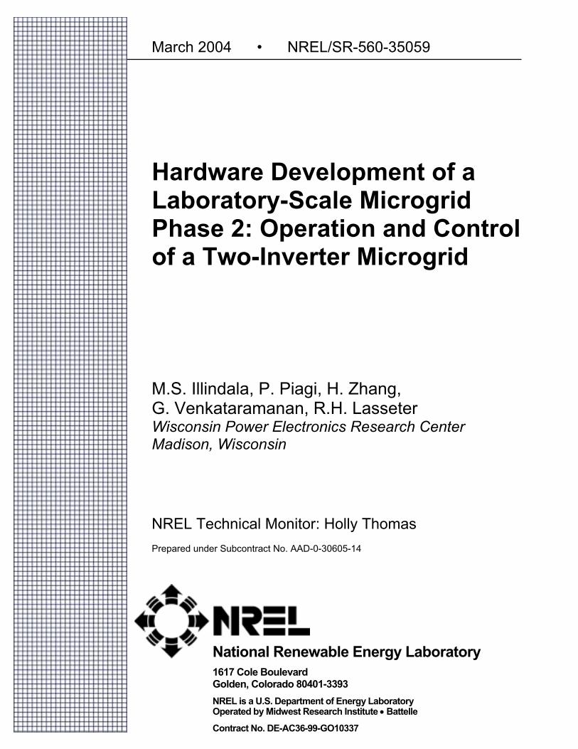
Electric utilities have traditionally responded to customer needs for reliable electric supply with a high degree of satisfaction. This has been achieved through increased capital investment in generation, transmission, and distribution infrastructure. Increased investments to maintain a quality infrastructure were possible in a regulated economic scenario of guaranteed prices and returns. However, in the unfolding deregulated operating environment, electric utilities face a competitive marketplace in which it is increasingly difficult to commit capital expenses to meet the needs of select customers. The problem is exacerbated by the fact that increasing demand for power quality by customers has coincided with reduced availability of capital for infrastructure investment. In addition, technologies such as dynamic voltage restorers that are necessary to provide ultra-reliable power supply for large and sensitive customers are just becoming available. Faced with such a scenario, some sensitive consumers of electricity have installed large uninterruptible power supply (UPS) systems to meet contingent situations. This is particularly common in the information industry. UPS systems convert utility power into DC power, which is stored in large battery banks and then converted back into AC to feed customer equipment. This solution is expensive; the initial cost of the equipment is high, and the operating cost is also high because of losses. But the demand for UPS and standby power supply equipment has been growing rapidly, illustrating the severity of the problem. To address this problem, concepts such as custom power and premium power have been proposed—with modest success. Typically, these do not integrate distributed power generation into solutions to the sensitive-load problem. Recent investigations have shown a high degree of match between the capabilities of DR and the demands of sensitive loads and that DR can be a viable and competitive solution to the problem. This project addresses the control and placement of DR as a solution to the sensitive-load problem. 1.2 Distributed Generation Small distributed generation (DG) technologies such as microturbines, photovoltaics, and fuel cells are gaining interest because of rapid advances in technology. The deployment of these generation units on distribution networks could potentially lower the cost of power delivery by placing energy sources nearer to demand centers. The capacity of the devices ranges from 1 kW to 2 MW. However, the trends in technology point toward generation units less than 500 kW. One cost-effective DG technology is a small, gas-fired microturbine in the 25–100-kw range that can be mass-produced. It is designed to combine the reliability of an on-board commercial aircraft generator with the low cost of an automotive turbocharger. A block diagram of such a system is illustrated in Figure 1. This prime mover is a high-speed turbine (50,000–90,000 rpm) with airfoil bearings. The AC generator coupled to the turbine typically generates power at 1–2 kHz. It is rectified into DC. A three-phase inverter converts the DC power into utility-grade AC power for the load. Examples include Allison Engine Co.'s 50-kW generator and Capstone's 30-kW system.
3
Rectifer Inverter3 phase
acoutput
gasfired
turbine
high speedgenerator
dclink
Figure 1. Block diagram of microturbine power generation system
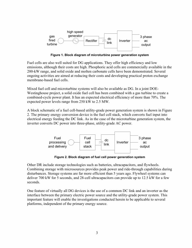
Fuel cells are also well suited for DG applications. They offer high efficiency and low emissions, although their costs are high. Phosphoric acid cells are commercially available in the 200-kW range, and solid oxide and molten carbonate cells have been demonstrated. Several ongoing activities are aimed at reducing their costs and developing practical proton exchange membrane-based fuel cells. Mixed fuel cell and microturbine systems will also be available as DG. In a joint DOE-Westinghouse project, a solid oxide fuel cell has been combined with a gas turbine to create a combined-cycle power plant. It has an expected electrical efficiency of more than 70%. The expected power levels range from 250 kW to 2.5 MW. A block schematic of a fuel cell-based utility-grade power generation system is shown in Figure 2. The primary energy conversion device is the fuel cell stack, which converts fuel input into electrical energy feeding the DC link. As in the case of the microturbine generation system, the inverter converts DC power into three-phase, utility-grade AC power.
Inverter3 phase
acoutput
dclink
Fuelcell
stack
Fuelprocessingand delivery
Figure 2. Block diagram of fuel cell power generation system
Other DR include storage technologies such as batteries, ultracapacitors, and flywheels. Combining storage with microsources provides peak power and ride-through capabilities during disturbances. Storage systems are far more efficient than 5 years ago. Flywheel systems can deliver 700 kW for 5 seconds, and 28-cell ultracapacitors can provide up to 12.5 kW for a few seconds. One feature of virtually all DG devices is the use of a common DC link and an inverter as the interface between the primary electric power source and the utility-grade power system. This important feature will enable the investigations conducted herein to be applicable to several platforms, independent of the primary energy source.

4
1.3 Development Scenarios for Distributed Generation DG systems provide utilities an alternative to the traditional investments made by electrical distribution companies. As demand increases, or becomes uncertain, DG resources make it possible to defer or delay indefinitely traditional capacity improvements by distributing generation and storage throughout the system. To meet certain customer demands on reliability and power levels, it may be less expensive to apply DG locally at a load location than to upgrade and provide the same level of service to all customers. Integrated service companies, which provide gas and electricity, may have an incentive to provide electricity through local generation and heat as a co-product to the same customer at the same location, thereby maximizing resource use. DG devices may be purchased and installed by consumers of electric power in various commercial and industrial settings to supplement electric power purchased from utilities. In such settings, they may also be used instead of more traditional standby or emergency electric power generation systems based on reciprocating engine-generator sets. The capital costs associated with DG systems range from $500/kW to $5,000/kW for technologies ranging from turbogenerators to fuel cells and solar photovoltaics. This is considered high to provide the “market pull” necessary to be applied widely in either of the above scenarios. For these technologies to become widespread and realize their fullest potential, they first need to be applied in less cost-sensitive applications—such as supplying sensitive loads in industrial and commercial settings—to gain acceptance. This scenario will allow DG technologies to be adopted by high-performance applications. As they gain acceptance in the marketplace and the technologies mature, they will see more penetration in the power network. Hence, there is a need to definitively establish the feasibility of DG devices to solve sensitive-load problems. 1.4 Distributed Generation for Sensitive Loads UPS systems and custom power devices provide alternative approaches to delivering ultra-reliable power to sensitive load centers. UPS systems typically use battery energy storage to provide power to sensitive loads. Custom systems for controlling voltage disturbances use a voltage source inverter, which injects reactive power into the system to achieve voltage correction. One method is to inject shunt reactive current; the other is to inject series voltage. These systems are effective in protecting against single-phase voltage sags (or swells) because of distant faults or imbalanced loads. These systems are costly, complex, and needed only during voltage disturbance events. It is clear that DG devices can increase reliability and power quality by being placed near the load. This provides for a stiffer voltage at the load and UPS functions during loss of grid power. At a more subtle level, the power electronic interface found on virtually all DG devices—namely, the inverter—has the potential to control voltage sags and imbalances.

5
Hence, through the appropriate implementation of control functions and the integration of storage into the systems, DG devices can be made to provide additional functionality that is superior to UPS systems and custom power devices. This will result in a more robust system for protection against single-phase voltage drops and swells. However, state-of-the-art DG devices have not been capable of providing such functionalities in a definitive manner. Hence, it is necessary to develop techniques to provide these functionalities and demonstrate them in hardware before they are deployed in the field. It is the broad objective of this proposal to demonstrate such features. 1.5 Technical Challenges DG devices are fundamentally different from conventional central station generation technologies. For instance, fuel cells and battery storage devices have no moving parts and are linked to the system through electronic interfaces. Microturbines have extremely lightweight moving parts and also use electronic interfaces. The dynamic performance of such inertia-less devices cannot be modeled as if they were simply scaled-down central station units. One large problem is the fact that microturbines and fuel cells have slow response and are inertia-less. It must be remembered that current power systems have storage in generators’ inertia. When a new load comes online, the initial energy balance is satisfied by the system’s inertia. This results in a slight reduction in system frequency. A system with clusters of microgenerators could be designed to operate in an island mode and provide some form of storage to provide the initial energy balance as “virtual inertia.” A system with clusters of microgenerators and storage could be designed to operate in both island and satellite mode, connected to the power grid. It is essential to have good control of the power angle and voltage level by means of the inverter. Control of the inverter's frequency dynamically controls the power angle and the flow of real power. To prevent overloading the inverter and the microsources, it is important to ensure that the inverter takes up load changes in a predetermined manner, without communication. The control of inverters used to supply power to an AC system in a distributed environment should be based on information available locally at the inverter. In a system with many microsources, communication of information between systems is impractical. Communication may be used to enhance system performance, but it must not be critical for system operation. This implies that inverter control should be based on terminal quantities. More than 90% of voltage disturbances in utility lines are single-phase voltage sags caused by momentary line-to-ground faults in distribution systems. Hence, the control strategy of the inverter should meet situations in which the utility grid has residual imbalances in voltage and the load system has imbalances in current [1]. When multiple units are connected in parallel at the same location or in close proximity, thereby forming a “microgrid,” the individual inverters should be capable of sharing active and reactive power in a predetermined manner, and circulating power should be avoided.
6
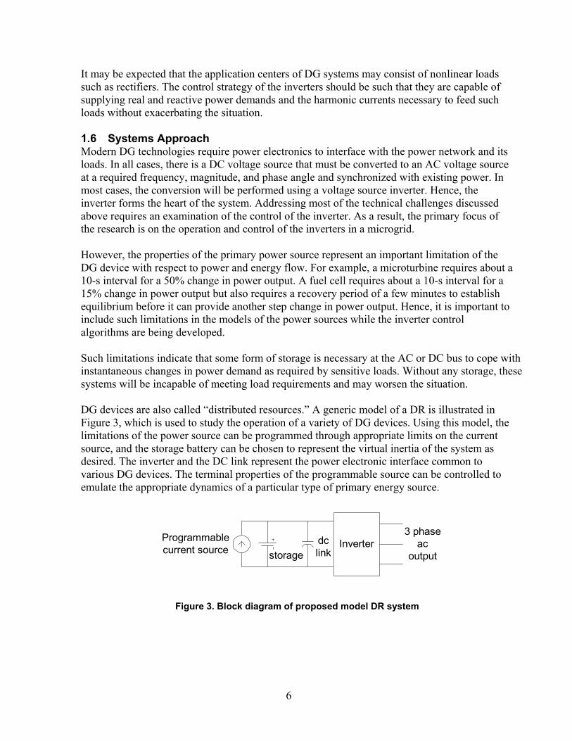
It may be expected that the application centers of DG systems may consist of nonlinear loads such as rectifiers. The control strategy of the inverters should be such that they are capable of supplying real and reactive power demands and the harmonic currents necessary to feed such loads without exacerbating the situation. 1.6 Systems Approach Modern DG technologies require power electronics to interface with the power network and its loads. In all cases, there is a DC voltage source that must be converted to an AC voltage source at a required frequency, magnitude, and phase angle and synchronized with existing power. In most cases, the conversion will be performed using a voltage source inverter. Hence, the inverter forms the heart of the system. Addressing most of the technical challenges discussed above requires an examination of the control of the inverter. As a result, the primary focus of the research is on the operation and control of the inverters in a microgrid. However, the properties of the primary power source represent an important limitation of the DG device with respect to power and energy flow. For example, a microturbine requires about a 10-s interval for a 50% change in power output. A fuel cell requires about a 10-s interval for a 15% change in power output but also requires a recovery period of a few minutes to establish equilibrium before it can provide another step change in power output. Hence, it is important to include such limitations in the models of the power sources while the inverter control algorithms are being developed. Such limitations indicate that some form of storage is necessary at the AC or DC bus to cope with instantaneous changes in power demand as required by sensitive loads. Without any storage, these systems will be incapable of meeting load requirements and may worsen the situation. DG devices are also called “distributed resources.” A generic model of a DR is illustrated in Figure 3, which is used to study the operation of a variety of DG devices. Using this model, the limitations of the power source can be programmed through appropriate limits on the current source, and the storage battery can be chosen to represent the virtual inertia of the system as desired. The inverter and the DC link represent the power electronic interface common to various DG devices. The terminal properties of the programmable source can be controlled to emulate the appropriate dynamics of a particular type of primary energy source.
Inverter3 phase
acoutput
dclink
Programmablecurrent source storage
Figure 3. Block diagram of proposed model DR system
7
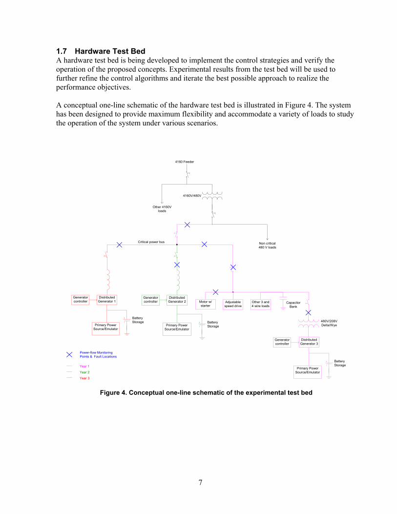
1.7 Hardware Test Bed A hardware test bed is being developed to implement the control strategies and verify the operation of the proposed concepts. Experimental results from the test bed will be used to further refine the control algorithms and iterate the best possible approach to realize the performance objectives. A conceptual one-line schematic of the hardware test bed is illustrated in Figure 4. The system has been designed to provide maximum flexibility and accommodate a variety of loads to study the operation of the system under various scenarios.
Critical power bus
DistributedGenerator 1 Motor w/
starterAdjustablespeed drive
Other 3 and4 wire loads
Non critical480 V loads
CapacitorBank
Primary PowerSource/Emulator
Generatorcontroller
Battery Storage
Power-flow MonitoringPoints & Fault Locations
4160V/480V
Other 4160Vloads
4160 Feeder
Year 1 Primary PowerSource/Emulator
Generatorcontroller
Battery Storage
DistributedGenerator 3
480V/208VDelta/Wye
DistributedGenerator 2
Battery Storage
Generatorcontroller
Primary PowerSource/Emulator
Year 2
Year 3
Figure 4. Conceptual one-line schematic of the experimental test bed

8
The test bed is being commissioned in phases over the period of the project. In its complete version, the experimental system will feature:
• A directly interfaced DR system • A transformer-coupled DR system • The possibility of standalone operation • The possibility of grid-interfaced operation • Induction motor loads • Adjustable speed drive loads • Four-wire systems • Single-phase loads • AC-side capacitor banks.
The components and interconnection infrastructure necessary for the experimental test bed are located at the Electrical and Computer Engineering Department’s power laboratory at the University of Wisconsin-Madison. The laboratory infrastructure facilitates such flexible interconnections in a systematic and safe manner. As reported in the first-year annual report [1], the first DR was commissioned in Phase I to operate as a standalone unit. The DR uses a programmable DC power source feeding the DC bus of the inverter. Because the inverter in the DR operates on pulse-width modulation (PWM), an LCL circuit consisting of a switching ripple LC filter along with a reactor is employed to suppress the switching ripples of the inverter. Furthermore, a delta-wye transformer is used to avoid DC injection into the distribution network. The transformer secondary is connected to a bus structure in which flexibility is provided to connect various loads and/or tie lines to the remaining part of the microgrid network. During Phase 2 of the project, the laboratory microgrid was expanded to include the second DR, which is identical to the first DR in size and rating. The connection between the two DR is through a contactor at the tie line interconnect; the connection between the microgrid and the main/grid supply is through a static switch. Circuitry containing synchronizing logic between two voltage sources was developed and installed in the microgrid to operate the contactor and the static switch. Switchgear was included in the microgrid to safeguard the equipment and personnel from injury. Power-measuring apparatus was placed at select locations in the microgrid where it was desired to monitor the power flow and record data. The digital signal processor (DSP) platform of the DR is used to test regulation and generation control algorithms in standalone and grid-interface modes of operation.

9
1.8 Report Organization Chapter 2 of the report explains the various power quality events that occur in a power system and their repercussions on sensitive loads. The role of a microgrid to circumvent the effects of power quality events is discussed, and a detailed description of the microgrid and its essential components is included. A case study of a microgrid consisting of two DR to supply power to an office-cum-warehouse facility is presented in Chapter 3. Chapter 4 presents a control strategy for the DR in the microgrid to provide a regulated voltage even under power quality events. The inverter is also equipped with generation control functionality to allow parallel operation with other inverters. Chapter 5 contains the practical implementation issues experienced while working with the hardware setup that is run using a DSP. Finally, Chapter 6 contains the conclusions of the report.

10
2 Microgrids With Power Quality Conditioning This chapter explains the power quality phenomena in the distribution system that affect the reliability of the power supply to sensitive loads. Traditional solutions to power quality problems are discussed, and the use of a microgrid as a preferred solution is presented. A microgrid consisting of two DR is outlined, and its essential components are identified. 2.1 Power Quality Events Various developments in recent years in the technology sector have brought dramatic improvements in productivity and performance. The number of loads that are sensitive to power quality has multiplied, and new technology has resulted in more electronic sources and loads that can trigger electromagnetic disturbances or be sensitive to such events. The term power quality refers to a variety of electromagnetic phenomena that characterize voltage and current at a given time and location on the power system [2]. The International Electrotechnical Commission [3] classifies electromagnetic phenomena into categories such as conducted and radiated low- and high-frequency events. Among these, the low-frequency conducted phenomena such as voltage imbalances, sags (dips), swells, and harmonics are significant and, hence, discussed in this project. In general, power quality events pertain to an abnormality in the voltage waveform with respect to its fundamental frequency sinusoidal waveform of nominal amplitude. The variation in voltage in each case is either of different magnitude or duration. Institute of Electrical and Electronics Engineers (IEEE) standard 1159-1995 has defined various power quality disturbance phenomena [2]. Voltage imbalance in a three-phase system is defined as the maximum deviation among the three phases from the average three-phase voltage divided by the average three-phase voltage. In other words, it is the ratio of the negative or zero sequence component to the positive sequence component. It is usually expressed as a percentage. Voltage imbalances of less than 2% are regularly caused by imbalanced single-phase loads on a three-phase circuit. Imbalances that are more severe (more than 5%) are generally because of single-phasing conditions. According to IEEE 141-1993 (Red Book) [4], mathematically, Voltage imbalance = 100 x (max deviation from average voltage)/average voltage A voltage sag is characterized as a decrease in voltage to between 0.1 and 0.9 pu in rms at the power frequency for durations of 0.5 cycle to 1 min. Sags are usually associated with faults in the power system, but they may also be incited during switching of heavy loads or the starting of large motors. Undervoltage events that last longer than 1 min may be associated with a variety of causes other than system faults. Likewise, an increase in voltage to between 1.1 and 1.8 pu in rms at the power frequency for durations of 0.5 cycle to 1 min is a voltage swell. Swells are usually associated with system faults but are less common than voltage sags. A swell takes place on the unfaulted phases of a system when a single line-ground fault is created. Swells can also be caused by switching off a large load or switching on a large capacitor bank. The severity of a sag or swell during a fault condition is a function of the fault location, system impedance, and grounding.

11
A harmonic is defined as a component of order greater than one of the Fourier series of a periodic quantity such as the AC current or voltage. Harmonics are introduced into a power system by nonlinear characteristics of devices and loads in the power system. The growing use of power electronics equipment has led to an increase in the percentage of harmonic content in the power system. The IEEE 519-1992 gives the admissible harmonic specifications in a power distribution system [5]. Harmonic distortion levels can be characterized by the complete harmonic spectrum with the magnitudes and phase angles of each individual harmonic component. However, it is common to use a single quantity, total harmonic distortion, as a measure of the harmonic distortion. 2.2 Effects on Sensitive Loads Common power quality problems such as voltage sags, voltage swells, voltage spikes, and short-term outages have been estimated to cost the U.S. economy $26 billion annually [6]. The losses are due to the loss of productivity in the downtime of sensitive loads caused by power quality events. The effect of power quality events on sensitive loads that take a considerable time to restore to normal operation is considered equivalent to a blackout for the same duration. Some of the loads that are sensitive to power quality are computers and electronic data-processing equipment. These sensitive loads have tolerance levels for supply voltage commonly specified by the Information Technology Industry/Computer and Business Equipment Manufacturers’ Association (ITI/CBEMA) curves, as shown in Figure 5 [7]. When the supply voltage falls outside the envelope of curves, the equipment typically stops functioning. As seen in Figure 5, the steady-state range of tolerance for computer equipment is ±10% from the nominal voltage (i.e., the equipment continues to operate normally when sourced by any voltages in this range for an indefinite period of time). Similarly, voltage swells to a magnitude 120% of the nominal value can be tolerated for about 0.5 s or 30 cycles; voltage sags to 80% of nominal for 10 s or 600 cycles can be tolerated. When the supply voltage is outside the boundaries of the susceptibility curves, improvement of power quality supplied to sensitive loads is essential to avoid an operation failure.
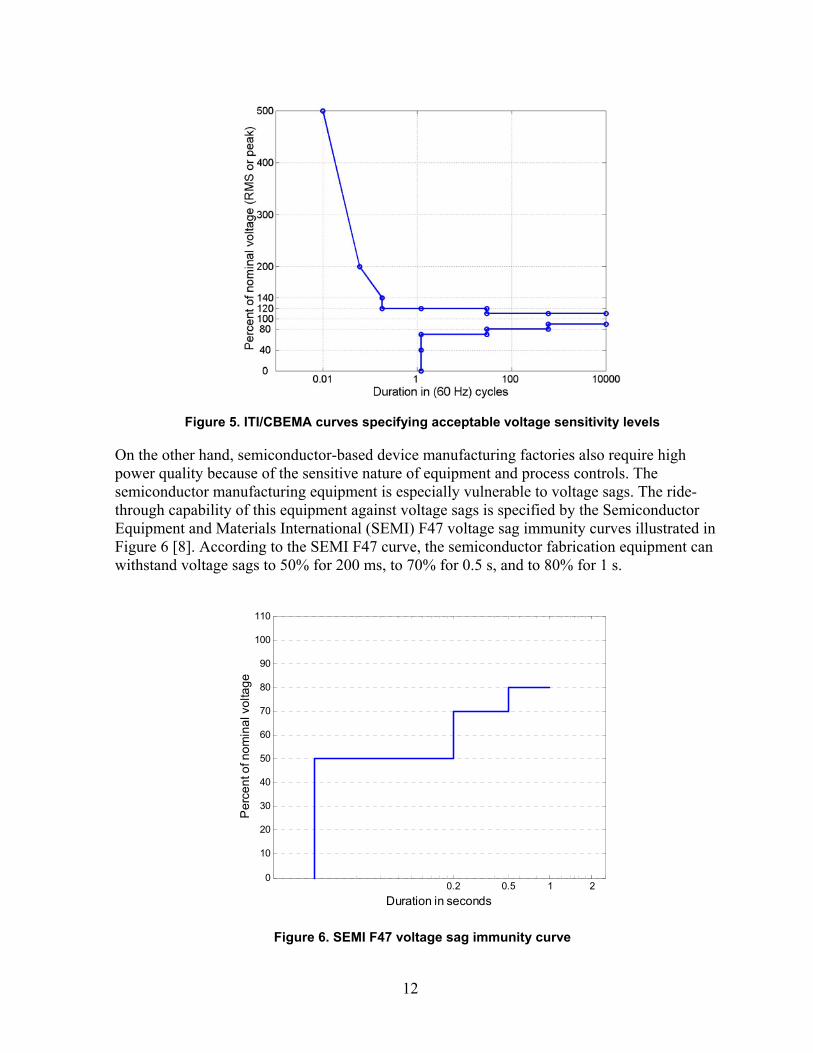
12
Figure 5. ITI/CBEMA curves specifying acceptable voltage sensitivity levels
On the other hand, semiconductor-based device manufacturing factories also require high power quality because of the sensitive nature of equipment and process controls. The semiconductor manufacturing equipment is especially vulnerable to voltage sags. The ride-through capability of this equipment against voltage sags is specified by the Semiconductor Equipment and Materials International (SEMI) F47 voltage sag immunity curves illustrated in Figure 6 [8]. According to the SEMI F47 curve, the semiconductor fabrication equipment can withstand voltage sags to 50% for 200 ms, to 70% for 0.5 s, and to 80% for 1 s.
Figure 6. SEMI F47 voltage sag immunity curve
0.2 0.5 1 20
10
20
30
40
50
60
70
80
90
100
110
Duration in seconds
Per
cent
of n
omin
al v
olta
ge

13
Similar examples for sag performance for programmable logic controllers, programmable logic controller input devices, adjustable speed drives, electromechanical relays, and starters are provided in IEEE 1346-1998 [9]. In any facility containing sensitive equipment, by compiling yearly sag data, it is possible to predict the number of events per year that will disrupt the performance of the sensitive equipment in the form of coordination charts. 2.3 Power Quality Solutions The methods recommended to avoid or minimize the effects of power quality incidents such as sags and swells can be applied at the customer end or the utility end [10]. Although custom power devices such as dynamic voltage restorers and static compensators are typical solutions offered to the utilities, the UPS is a common solution suggested to the customer. Nonetheless, an optimal solution depends on factors such as the severity and source of the power quality event. The customer solution of UPS typically provides AC voltage to the load when the grid fails. Backup generation systems based on rotating machines may be used as an alternative to a UPS system to supply power to sensitive loads during temporary interruptions in grid power supply. However, such systems require a start-up time to deliver power, which would cause a brief interruption in the operation of sensitive loads. More recently, electrical generation systems that are dispersed and located near the load centers, commonly known as microsource DG, are gaining popularity. DG comprises small electrical generation sources at load centers that optimally use energy resources. It can be used to provide energy stabilization, ride-through, and dispatchability [11]. DG energy includes solar (photovoltaics), wind, and microsources such as microturbines and fuel cells. Among these, sources such as solar or wind power may be used to provide auxiliary support only and not as primary generation sources for sensitive loads because they are not dispatchable. Nevertheless, microturbines and fuel cells are dispatchable and considered as a solution to the sensitive-load problem. The utility-to-load interfaces of microsources such as microturbines or fuel cells incorporate power electronic converters. In this report, when the microsources are combined with energy storage, they are called “distributed resources.” The energy storage device of the DR provides the ride-through for the transient load demand [12]. The DR are capable of providing reliable power supply to sensitive loads when connected in the formation of a microgrid [13, 14]. 2.4 Microgrid The simplified schematic of a microgrid consisting of two DR is illustrated in Figure 7. It consists of two DR—DR1 and DR2—and the utility grid supply. As shown in the figure, the PWM switching of the power electronic converter in each DR necessitates the installation of an LCL filter. Furthermore, there is a delta-wye transformer along with each DR to essentially provide a neutral terminal for the single- and three-phase loads.
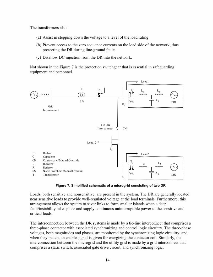
14
The transformers also:
(a) Assist in stepping down the voltage to a level of the load rating
(b) Prevent access to the zero sequence currents on the load side of the network, thus protecting the DR during line-ground faults
(c) Disallow DC injection from the DR into the network.
Not shown in the Figure 7 is the protection switchgear that is essential in safeguarding equipment and personnel.
GridInterconnect
Lf2Lt2
Cf2
Lt1
Cf1
Lf1T2
T3
Tie-lineInterconnect
T1 SS1
B1
B2
B3
Load12
Load1
Load2
∆ -Y Y-∆
Y-∆
CN1
B BusbarC CapacitorCN Contactor w/ Manual OverrideL InductorR ResistorSS Static Switch w/ Manual OverrideT Transformer DR2
DR1
Figure 7. Simplified schematic of a microgrid consisting of two DR
Loads, both sensitive and nonsensitive, are present in the system. The DR are generally located near sensitive loads to provide well-regulated voltage at the load terminals. Furthermore, this arrangement allows the system to sever links to form smaller islands when a deep fault/instability takes place and supply continuous uninterruptible power to the sensitive and critical loads. The interconnection between the DR systems is made by a tie-line interconnect that comprises a three-phase contactor with associated synchronizing and control logic circuitry. The three-phase voltages, both magnitudes and phases, are monitored by the synchronizing logic circuitry, and when they match, an enable signal is given for energizing the contactor coil. Similarly, the interconnection between the microgrid and the utility grid is made by a grid interconnect that comprises a static switch, associated gate drive circuit, and synchronizing logic.
15
2.4.1 Static Switch When a fault occurs on the utility grid, the grid interconnection is instantaneously disabled, and the DR is used to support the loads. This prevents sensitive loads from being affected by the fault. Figure 8 shows the details of the power circuit of the static switch [15].
R
C
MOV R
C
MOVR
C
MOV
Snubber Circuit Board
SynchronizationControl Board
1 3 5 2 4 6
SCR FIRINGBOARD
FIRINGSIGNAL
208VAC
60Hz
3Φ
Figure 8. Power circuit schematic of the static switch
The static switch, which consists of three pairs of anti-parallel silicon-controlled rectifiers (SCRs), enables seamless transfer of energy from the power grid or DG to the loads to avoid service interruption upon a power quality deficiency. Because the three-phase line is rated at 208 V, and in the worst case the voltage across the SCRs is totally out of phase, the SCRs are rated at 1600 V, which provides a healthy safety factor. In addition to the SCRs, there is a three-phase snubber circuit, which consists of a series resistance-capacitance paralleled with a metal-oxide-varistor connected across the SCRs. For the SCRs, a high rate-of-rise voltage, or dV/dt, occurs when they cease conduction or are gated into conduction. Also, high peak voltage is produced when an inductive circuit connected to the SCRs is interrupted. The function of the resistor/capacitor in the snubber board is to limit dV/dt and metal-oxide-varistor limits peak voltage.
16
The most important function of the static switch is reclosing upon restoration of normal grid conditions. A synchronization controller is used for this purpose. It monitors instantaneous voltages across the SCRs. When the difference between the two is less than 5% of the nominal voltage level, the output gives a logic signal to the SCR firing board, which then triggers all the three-phase SCRs at the same time. By using the static switch, power quality problems become transparent to the critical or sensitive customer loads. However, one of the major issues of the static switch is power loss in solid-state semiconductor devices. In the static switch, line current flows in the devices continuously, causing power consumption and element heating during normal operation. As a result, relatively large cooling equipment is required, which imposes additional operating costs to limit SCR temperature. It also results in reduced efficiency and lower reliability in the device. Therefore, the heat sink and cooling function selection is critical. Another important issue is the speed of operation of the static switch, which is primarily determined by the switching time. The switching time is of importance because it identifies the duration of power discontinuity/interruption for the sensitive load. The duration of power discontinuity is the key factor in predicting proper operation of the load. The static switch must be able to perform a fast transfer from the distributed source to the healthy grid regardless of the load type and the fault/disturbance characteristics. 2.4.2 Static Switch/Contactor Controller It is clear that the critical aspect of static switch operation is the synchronization control. The reliability of the system depends on whether the static switch can close the local load to the grid only when the voltages are synchronized. Usually, this can be achieved by comparing the phase of the voltage of the load bus with the oncoming grid source and transferring at the first window of opportunity (i.e., when the sources are close enough in phase and amplitude to produce an acceptably small disturbance when the grid is applied). Figure 9 shows the principal circuit of the synchronizing logic for one phase of the monitoring circuit.
Figure 9. Schematic of the static switch/contactor control circuit

17
The voltages across the static switch when they are close to synchronization appear as a power frequency waveform, with amplitude modulated by the beat frequency of the difference between them. The static switch or contactor needs to be closed when the modulated waveform is near 0. Essentially, the circuit attenuates the voltage difference and sends it to a demodulator. The demodulator—formed by the diode 1N4148, the 50-kΩ resistor, and the 4.7-µF capacitor—is similar to the one commonly used in AM radio receiver sets. The demodulated signal is then set to a voltage comparator (LM311). The output of the comparator is used to change the state of a D flip-flop if the flip-flop is enabled. The enable condition is determined by either a manual toggle switch or DSP control signal. When it is decided to close the static switch/contactor, the enable signal is a logical high, and the first rising edge at the comparator output (signifying synchronism) makes the output logical low. All the three-phase outputs through a triple input NOR gate control a solid-state relay, which either sends a 5-VDC drive signal to the static switch or energizes the contactor coil. The controller can be tuned such that the threshold level of synchronization can be varied from 5% to 10% using a potentiometer. Furthermore, during synchronization, it is assumed that a balanced three-phase system appears across the switch. Only when the differences of voltages of all three phases are under the set synchronization level, the static switch/contactor will close. This chapter described the power quality phenomena that affect the reliability of power supply to sensitive loads. Traditional solutions were discussed, and the use of microgrid as a preferred solution was presented.
18
3 Microgrid: A Case Study This chapter provides a case study of an office-cum-warehouse facility. In this chapter, a two-inverter microgrid is analytically modeled. The component sizing is according to the voltages and currents that must be withstood while allowing the necessary power flow. Characteristics of the system such as voltage regulation, real and reactive power flow, and load features are investigated. Three-phase balanced linear loads are distributed throughout the microgrid. The scope of operation of the system to meet the demands of changing load conditions is determined. 3.1 Components of the Microgrid The equipment in the microgrid in Figure 10 is further discussed in the following paragraphs.
Figure 10. Schematic of a microgrid for an office-cum-warehouse facility
100ft
L
E
A
ACAC
L
L
L
L
L
C
L L
2nd Floor
1st Floor
2nd Floor 1st
Floor
OFFICE 150kW
WAREHOUSE 100kW
BUSBAR
T1
T2
1.5MV
480V
13.8kV
BUSBARS
10 mi1 mi. aerial 1mi.
1
2MVA
120kV 13.8kV
Substation (Ideal Source)
43 2 3
8
37 36
15
38
39
40
41
4
35 34
13
T3
480V
208V
0.3M
14
11
32
12
33
Ceiling
L
DR 1
DR 2
L
L – Lighting C – Computer AC – Air conditioner
19
It is possible to break up the electrical diagram into three distinct groups: transformers, loads, and branches. It is also possible to compare models and connections for the components of the network from the following tables. Transformer data is summarized in Table 1, in which the voltages, ratings, and connection types are listed.
Table 1. Transformer Summary for Microgrid Case Study
Transformer #
V_Primary [kV]
V_Secondary [kV]
Actual Load [kW]
Rating [kVA] Connection
Available Voltage [V]
1 120 13.8 1000 2000 delta-wye-n - 2 13.8 0.480 440 1500 delta-wye-n 480, 280 3 0.480 0.208 150 300 delta-wye-n 208, 120
Loads are summarized in Table 2, in which utilization voltage, connection type, and sizes are listed. The table also shows which model is used to represent the load in the electrical network.
Table 2. Load Summary for Microgrid Case Study
Load Type Voltage Level [V] Connection
Sizes [kW]
Power Factor Model Quantity
AC Systems
280 Three-ph. LN 15, 30, 40 0.95 LN equiv. impedance
3
Elevators 480 Three-ph. wye-n
30 0.97 LN equiv. impedance
1
Lights 120 Single-ph. LN 5, 10, 15, 30
0.98 LN equiv. impedance
5
Computers 120 Single-ph. LN 50 0.96 LN equiv. impedance
1
Table 3 summarizes the properties of each of the branches responsible for distributing the power along the plant. The voltage level, ratings, and cable type are listed with the theoretic and allowable current per phase.
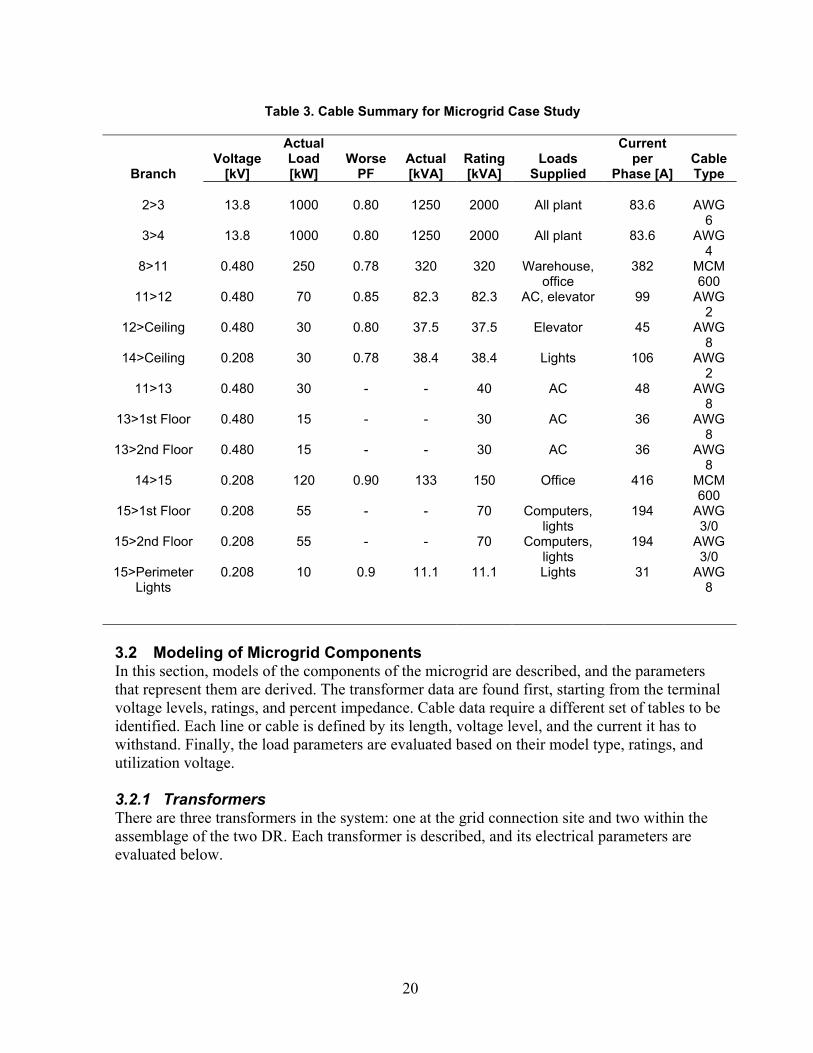
20
Table 3. Cable Summary for Microgrid Case Study
Branch
Voltage [kV]
Actual Load [kW]
Worse PF
Actual [kVA]
Rating[kVA]
Loads Supplied
Current per
Phase [A]Cable Type
2>3 13.8 1000 0.80 1250 2000 All plant 83.6 AWG
6 3>4 13.8 1000 0.80 1250 2000 All plant 83.6 AWG
4 8>11 0.480 250 0.78 320 320 Warehouse,
office 382 MCM
600 11>12 0.480 70 0.85 82.3 82.3 AC, elevator 99 AWG
2 12>Ceiling 0.480 30 0.80 37.5 37.5 Elevator 45 AWG
8 14>Ceiling 0.208 30 0.78 38.4 38.4 Lights 106 AWG
2 11>13 0.480 30 - - 40 AC 48 AWG
8 13>1st Floor 0.480 15 - - 30 AC 36 AWG
8 13>2nd Floor 0.480 15 - - 30 AC 36 AWG
8 14>15 0.208 120 0.90 133 150 Office 416 MCM
600 15>1st Floor 0.208 55 - - 70 Computers,
lights 194 AWG
3/0 15>2nd Floor 0.208 55 - - 70 Computers,
lights 194 AWG
3/0 15>Perimeter
Lights 0.208 10 0.9 11.1 11.1 Lights 31 AWG
8
3.2 Modeling of Microgrid Components In this section, models of the components of the microgrid are described, and the parameters that represent them are derived. The transformer data are found first, starting from the terminal voltage levels, ratings, and percent impedance. Cable data require a different set of tables to be identified. Each line or cable is defined by its length, voltage level, and the current it has to withstand. Finally, the load parameters are evaluated based on their model type, ratings, and utilization voltage. 3.2.1 Transformers There are three transformers in the system: one at the grid connection site and two within the assemblage of the two DR. Each transformer is described, and its electrical parameters are evaluated below.

21
3.2.1.1 Transformer T1 This transformer, included in a substation cabin not far from the plant, is connected to the high-voltage aerial transmission line. The primary-side busbar is at 120 kV, and the secondary busbar is at 13.8 kV. The secondary busbar is connected to the distribution aerial line at 13.8 kV. This transformer carries the full load of the plant, or 1 MW. The size of this transformer is chosen to be 2 MW to meet this requirement and provide for future expansion. This transformer is delta-wye with the neutral solidly grounded on the secondary. It also has a variable tap changer. From the voltage levels and ratings, this transformer typically has a percent impedance of
6.75% and a ratio XR = 9.5. With this data, it is possible to obtain the transformer data as:
X = V2 Z%MVA =
1200002 0.06752000000 = 486 ohms
R = X
9.5 = 51.15 ohms
3.2.1.2 Transformer T2 This transformer is located close to T1 and is fed at its primary side by the distribution cable entering the plant. The secondary-side busbar is connected to the remaining 480-V load inside the factory to the cable that leads to the warehouse. This transformer is delta-wye connected and has a solidly grounded neutral at the secondary.
The percent impedance of this transformer is 5.7% and XR = 6.3. The reactance and resistance of
the transformer are: R = 7.23 ohms X = 1.15 ohms 3.2.1.3 Transformer T3 This transformer is located in the warehouse and is needed to feed loads at 208 V and 120 V in the warehouse and office buildings. The primary busbar is connected to the cable coming from the warehouse, and the secondary busbar is connected to two cables. The first reaches the ceiling of the warehouse; the other goes to a panel inside the office. The current load is 150 kW, and a transformer with a rating of 0.3 MVA is chosen to meet the demand and provide for future plans for expansion.
The percent impedance of this transformer is 3.4% and the ratio XR = 4.3, which yield:
X = 4802 0.034
300000 = 0.0261 ohms
R = X
4.3 = 0.0061 ohms
22
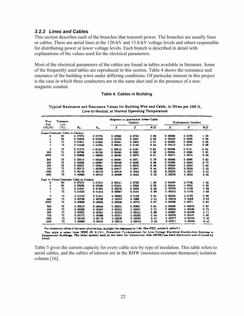
3.2.2 Lines and Cables This section describes each of the branches that transmit power. The branches are usually lines or cables. There are aerial lines at the 120-kV and 13.8-kV voltage levels and others responsible for distributing power at lower voltage levels. Each branch is described in detail with explanations of the values used for the electrical parameters. Most of the electrical parameters of the cables are found in tables available in literature. Some of the frequently used tables are reproduced in this section. Table 4 shows the resistance and reactance of the building wires under differing conditions. Of particular interest in this project is the case in which three conductors are in the same duct and in the presence of a non-magnetic conduit.
Table 4. Cables in Building
Table 5 gives the current capacity for every cable size by type of insulation. This table refers to aerial cables, and the cables of interest are in the RHW (moisture-resistant thermoset) isolation column [16].
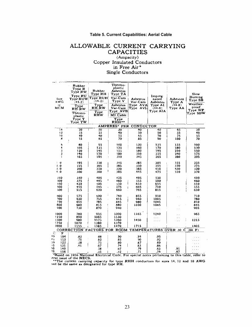
23
Table 5. Current Capabilities: Aerial Cable
24
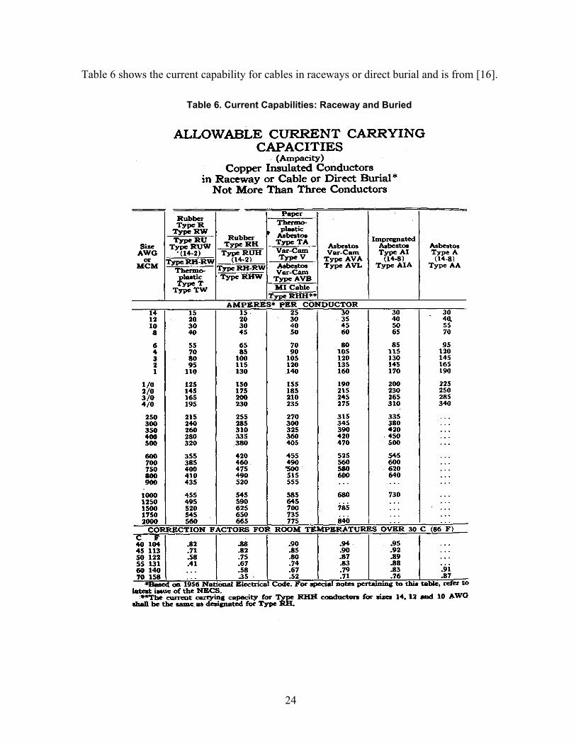
Table 6 shows the current capability for cables in raceways or direct burial and is from [16].
Table 6. Current Capabilities: Raceway and Buried
25
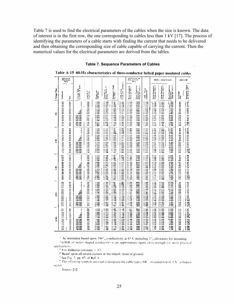
Table 7 is used to find the electrical parameters of the cables when the size is known. The data of interest is in the first row, the one corresponding to cables less than 1 kV [17]. The process of identifying the parameters of a cable starts with finding the current that needs to be delivered and then obtaining the corresponding size of cable capable of carrying the current. Then the numerical values for the electrical parameters are derived from the tables.
Table 7. Sequence Parameters of Cables
26
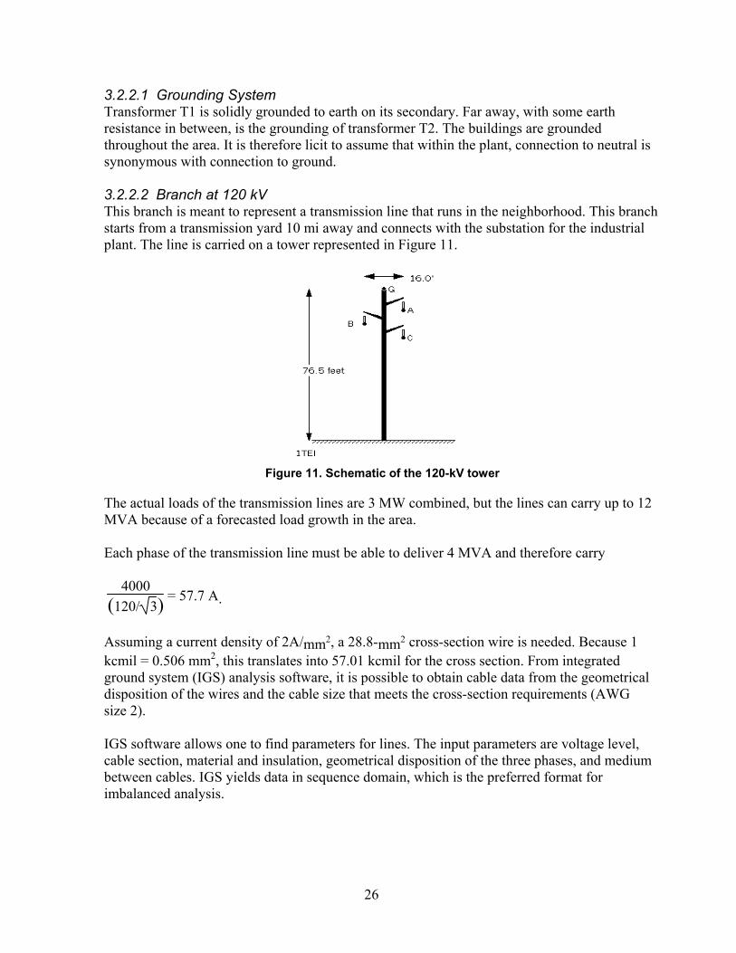
3.2.2.1 Grounding System Transformer T1 is solidly grounded to earth on its secondary. Far away, with some earth resistance in between, is the grounding of transformer T2. The buildings are grounded throughout the area. It is therefore licit to assume that within the plant, connection to neutral is synonymous with connection to ground. 3.2.2.2 Branch at 120 kV This branch is meant to represent a transmission line that runs in the neighborhood. This branch starts from a transmission yard 10 mi away and connects with the substation for the industrial plant. The line is carried on a tower represented in Figure 11.
Figure 11. Schematic of the 120-kV tower
The actual loads of the transmission lines are 3 MW combined, but the lines can carry up to 12 MVA because of a forecasted load growth in the area. Each phase of the transmission line must be able to deliver 4 MVA and therefore carry
4000( )120/ 3
= 57.7 A.
Assuming a current density of 2A/mm2, a 28.8-mm2 cross-section wire is needed. Because 1 kcmil = 0.506 mm2, this translates into 57.01 kcmil for the cross section. From integrated ground system (IGS) analysis software, it is possible to obtain cable data from the geometrical disposition of the wires and the cable size that meets the cross-section requirements (AWG size 2). IGS software allows one to find parameters for lines. The input parameters are voltage level, cable section, material and insulation, geometrical disposition of the three phases, and medium between cables. IGS yields data in sequence domain, which is the preferred format for imbalanced analysis.

27
For the 10-mi section, the results are: R1 = 8.541 ohms X1 = 11.003 ohms R0 = 11.741ohms X0 = 20.719 ohms For the 2-mi section, the data are: R1 = 1.7082 ohms X1 = 2.2006 ohms R0 = 2.3482 ohms X0 = 4.1438 ohms 3.2.2.3 Branch From Bus 2 to Bus 3 This is an aerial line using a single-pole distribution line with three-phase conductors placed at triangle. Neutral is also carried in the pole. The load is the whole plant, 1MW, and a conservative power factor of 0.8 brings the requirements for the apparent power to 1
0.8 = 1.25 MVA.
The nature of the plant loads with induction machines and the requirement that the line must satisfy further plant expansion suggest that a conservative rating of the transmission line over the three phases is 2 MVA.
Each phase must be able to transfer 2000
3 = 666 kVA.
Current per each phase: 666
( )13.8/ 3 = 83.6 A.
From Table 6 and for RHW insulation, it can be shown that AWG Size 6 is the conductor needed in this segment. From IGS software, after choosing the tower structure (shown in Figure 12) and selecting the cable size, the data relative to the 1-mi span of this aerial line is: R1 = 2.16 ohms X1 = 1.088 ohms R0 = 2.59 ohms X0 = 2.357 ohms
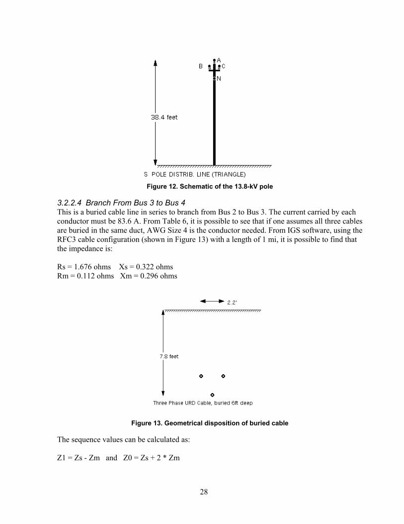
28
Figure 12. Schematic of the 13.8-kV pole
3.2.2.4 Branch From Bus 3 to Bus 4 This is a buried cable line in series to branch from Bus 2 to Bus 3. The current carried by each conductor must be 83.6 A. From Table 6, it is possible to see that if one assumes all three cables are buried in the same duct, AWG Size 4 is the conductor needed. From IGS software, using the RFC3 cable configuration (shown in Figure 13) with a length of 1 mi, it is possible to find that the impedance is: Rs = 1.676 ohms Xs = 0.322 ohms Rm = 0.112 ohms Xm = 0.296 ohms
Figure 13. Geometrical disposition of buried cable
The sequence values can be calculated as: Z1 = Zs - Zm and Z0 = Zs + 2 * Zm

29
The values are: R1 = 1.564 ohms X1 = 0.026 ohms R0 = 1.9 ohms X0 = 0.914 ohms 3.2.2.5 Branch From Bus 8 to Bus 11 This branch connects the secondary-side busbar of transformer T3 in the factory with the primary-side busbar of the transformer in the warehouse. The cable must be able to carry the load for the warehouse and offices. The current combined load is 250 kW.
To accommodate for a power factor of 0.78, 2500.78 = 320 kVA is obtained.
Each phase must deliver 106 kVA and carry 106
( )0.48/ 3 = 382 A.
From Table 6, cable size MCM 600 is needed. From Table 7: R1 = 0.113 ohm/mi X1 = 0.122 ohm/mi R0 = 2.74 ohm/mi X0 = 0.197 ohm/mi With the cable length of 500, it is possible to obtain: R1 = 0.113 * 500 / 4970 = 0.0114 ohm X1 = 0.122 * 500 / 4970 = 0.0123 ohm R0 = 2.74 * 500 / 4970 = 0.2757 ohm X0 = 0.197 * 500 / 4970 = 0.0198 ohm 3.2.2.6 Branch From Bus 11 to Bus 12 This branch starts from the primary-side busbar of the transformer in the warehouse and ends at the panel that connects with the cable that reaches the ceiling. Three conductors are in the same duct, and the loads are the air conditioning (AC) and lighting systems of the warehouse—a combined 70 kW. With an expected worse power factor of 0.85: 70
0.85 = 82.3 kVA.
Each phase must deliver 82.3
3 = 27.4 kVA and carry 27.4
( )0.48/ 3 = 99 A.
Table 6 indicates cable size AWG 2 is needed. From Table 7, the following data are obtained: R1 = 0.987 ohm/mi X1 = 0.165 ohm/mi R0 = 6.99 ohm/mi X0 = 0.273 ohm/mi

30
The length of this span is 50 ft. Therefore, the data are: R1 = 0.987 * 50 / 4970 = 0.0099 ohms X1 = 0.0017 ohms R0 = 0.0703 ohms X0 = 0.0027 ohms 3.2.2.7 Branch From Bus 12 to Ceiling This branch provides power to the elevator machinery located at the ceiling of the warehouse. The load for the elevator is 30 kW. With a worse power factor of 0.8, 300.8 = 37.5 kVA is obtained.
Each phase must supply 12.5 kVA and carry 12.5
( )0.48/ 3 = 45 A.
Table 6 indicates cable size AWG 8 is needed. From Table 4, with three conductors in the same duct, the following data are obtained: R = 0.07275 ohms/100 ft X = 0.00389 ohms/100 ft Because the length of this branch is 100 ft, the data are: R = 0.07275 ohms X = 0.00389 ohms 3.2.2.8 Branch From Bus 14 to Warehouse Lights This branch connects the low-side busbar of the transformer in the warehouse to the ceiling of the warehouse, where the light system is. The only loads are the lights, and the voltage is 208 V. The load is meant to be connected on a single-phase basis; therefore, there will be a single conductor per conduit. The power needed for the lights is 30 kW, and with a maximum power factor of 0.78 30
0.78 = 38.4 kVA is obtained.
Each phase must be able to supply 12.8 kVA and carry 12.8
( )0.208/ 3 = 106 A.
Table 6 indicates cable size AWG 2 is needed. From Table 4, the following data are obtained: R1 = 0.987 ohms/mi X1 = 0.165 ohms/mi R0 = 6.99 ohms/mi X0 = 0.273 ohms/mi This branch is 200 ft long. Hence, the data are: R1 = 0.987 * 200 / 4970 = 0.0397 ohms X1=0.165*200/4970=0.0066 ohms R0=6.99*200/4970= 0.2813 ohms X0=0.273*200/4970= 0.0110 ohms

31
3.2.2.9 Branch From Bus 11 to Bus 13 This branch connects the primary-side busbar of the transformer in the warehouse to the panel in the office in which cables for the first and second floor split. This branch provides 480-V service to the AC system of the office. Total load is 30 kW, but expansion needs require this cable to be capable of delivering 40 kVA.
Each phase must supply 13.3 kVA and carry 13.3
( )0.48/ 3 = 48 A.
Table 6 indicates cable size AWG 8 is needed. From the portion of Table 4 relevant to three conductors belted, the following data are obtained: R = 0.07275 ohms/100 ft X = 0.00389 ohms/100 ft The length of this branch is 100 ft, and the data are: R = 0.07275 ohms X = 0.00389 ohms 3.2.2.10 Branch From Bus 13 to First-Floor 480-V Office Loads This branch starts from the panel and reaches the AC system for the first floor. Total load is 15 kW. Expansion plans require the cable to be capable of supplying 30 kVA.
Each phase must deliver 10 kVA and carry 10
( )0.48/ 3 = 36 A.
Table 6 indicates cable size AWG 8 is needed. From Table 4, with three conductors in the same duct: R = 0.07275 ohms/100 ft X = 0.00468 ohms/100 ft This branch has to reach the office floors and is 200 ft long. The data are: R = 0.07275 * 2 = 0.1455 ohms X = 0.0094 ohms 3.2.2.11 Branch From Bus 13 to Second-Floor 480-V Office Loads This branch has requirements identical to those of the previous branch, but it is 30 ft longer to reach the second floor. Total length for this branch is 230 ft. The data are: R = 0.07275 * 2.3 = 0.1673 ohms X = 0.0108 ohms

32
3.2.2.12 Branch From Bus 14 to Bus 15 This branch connects the secondary busbar of the transformer in the warehouse with the 208-V panel in the office building. From this panel, cables will be directed to the two floors and the perimeter lights. The overall load for this branch is 120 kW, and the estimated worse power factor of 0.9 translates the requirement for the apparent power to 133 kVA. The cable is sized to accommodate the future administrative needs of the office and is rated for 150 kVA.
Each phase must deliver 50 kVA and carry 50
( )0.208/ 3 = 416 A.
Table 6 indicates cable size MCM 600 is needed. From Table 7, the following data are obtained: R1 = 0.113 ohms/mi X1 = 0.122 ohms/mi R0 = 2.74 ohms/mi X0 = 0.197 ohms/mi The length of this branch is 100 ft, and the data are: R1 = 0.113 * 100 / 4970 = 0.0023 ohms X1 = 0.122 * 100 / 4970 = 0.0025 ohm R0 = 2.74 * 100 / 4970 = 0.0551 ohms X0 = 0.197 * 100 / 4970 = 0.0040 ohm 3.2.2.13 Branch From Bus 15 to First-Floor 208-V Office Loads This floor has a mixture of light and computer-related loads. The overall demand is 55 kW, and it is mainly at 120 V, which means cables will run singularly inside each duct because of the single-phase nature of the loads. With the extra quota considered, the apparent quota requirement for this floor is 70 kVA.
Each phase must deliver 23.3 kVA and carry 23.3
( )0.208/ 3 = 194 A.
Table 6 indicates cable size AWG 3/0 is needed. From Table 7, with one conductor per conduit: R1 = 0.392 ohms/mi X1 = 0.134 ohms/mi R0 = 5.46 ohms/mi X0 = 0.241 ohms/mi The length of this branch is 150 ft. The data are: R1 = 0.392 * 150 / 4970 = 0.0118 ohms X1 = 0.134 * 150 / 4970 = 0.0040 ohms R0 = 5.46 * 150 / 4970 = 0.1648 ohms X0 = 0.241 * 150 / 4970 = 0.0073 ohms

33
3.2.2.14 Branch From Bus 15 to Second-Floor 208-V Office Loads This branch is identical to the previous one except that it is 30 ft longer to reach the second floor. The new length is 180 ft, and the data are: R1 = 0.392 * 180 / 4970 = 0.0142 ohms X1 = 0.134 * 180 / 4970 = 0.0049 ohms R0 = 5.46 * 180 / 4970 = 0.1977 ohms X0 = 0.241 * 180 / 4970 = 0.0087 ohms 3.2.2.15 Branch From Bus 15 to Perimeter Lights This branch provides power to the lights in the parking lots and around the perimeter of the industrial plant. Load is single-phase; therefore, the cable is run singularly for each conduit. The length is considered to be of 200 ft to the first light. There are then four subbranches of 100 ft each. At the end of each subbranch is a light. The power requirements for this cable are 10 kW, and with a power factor of 0.9 it has an
apparent rating of 100.9 = 11.1 kVA.
Each phase must deliver 3.7 kVA and carry 3.7
( )0.208/ 3 = 31 A.
Table 6 indicates cable size AWG 8 is needed. From Table 4, with one conductor per conduit: R = 0.07275 ohms/100 ft X = 0.00468 ohms/100 ft For the first part of 200 ft, the data are: R = 0.07275 * 2 = 0.1455 ohms X = 0.0094 ohms For each of the subbranches of 100 ft, the data are: R = 0.07275 ohms X = 0.00468 ohms 3.2.3 Loads This section describes the loads in detail. Each load is defined according to its location, rating, and connection with the distribution system. Every load has its own model, and a brief explanation describes how the electrical parameters for all loads in the plant were obtained. 3.2.3.1 Air Conditioning Systems There are three AC systems in the plant—one in each building. The size of each AC system is tailored to the needs of its particular environment. There is a centralized AC system of 40 kW for the larger warehouse, and there is a smaller system of two conditioners of 15 kW—one in each floor in the office building. The AC system is intended to be connected to the 480-V system, though using a 280-V supply, because the load is connected line to ground. The load is three-phase, each of the phases with the same amount of load. The connection is wye without grounding at the neutral.

34
To represent the conditioners with a series equivalent impedance, one only needs to specify a representative power angle. For this kind of load, it is safe to assume a power factor of 0.95. The impedances for the AC systems are:
• 40-kW system in warehouse:
Q = P tan(pf) = 40 tan(acos(0.95)) = 13.1 kVAR G = P/V2 = 0.1736 ohm-1, B = Q/V2 = 0.0569 ohm-1 Y2 = G2 + B2 = 0.0334 ohm-2 R = G/Y2 = 5.202 ohm, X = B/Y2 = 1.7037 ohm
• 15-kW system in office:
Q = P tan(pf) = 15 tan(acos(0.95)) = 4.9 kVAR G = P/V2 = 0.0651 ohm-1, B = Q/V2 = 0.0213 ohm-1 Y2 = G2 + B2 = 0.0047 ohm-2 R = G/Y2 = 13.879 ohm, X = B/Y2 = 4.5338 ohm
3.2.3.2 Elevators Elevators are present in all the environments in which it is routine to lift heavy equipment. The warehouse has only one elevator. Elevator size is the same for all: 30 kW. Elevators always operate at 480 V and are synchronous machines responsible for lifting the cabin as demanded. These machines are wye-connected with a floating neutral (i.e., no grounding is provided at the center of the star). This is to reflect asynchronous machine design, with coils connected in wye but with no direct path to ground. Therefore, a series equivalent impedance model can represent them. Synchronous machines can be internally compensated to a nearly unitary power factor. Here, a power angle of 0.97 is assumed for the elevators: Q = P tan(pf) = 30 tan(acos(0.97)) = 7.5 kVAR G = P/V2 = 0.1302 ohm-1, B = Q/V2 = 0.0326 ohm-1 Y2 = G2 + B2 = 0.018 ohm-2 R = G/Y2 = 7.2282 ohm, X = B/Y2 = 1.8071 ohm 3.2.3.3 Lights Each environment has its own light system. There are four kinds of lights. In the factory, each floor has a lighting load of 15 kW. The warehouse has 30 kW, and the office has 5 kW per floor. In addition, there are perimeter lights around the buildings and the parking lot. The external lights account for a 10-kW load (five lights of 2 kW each). Lights are very well internally compensated and have a power factor of 0.98. Their connection to the supply is always single-phase, line-to-neutral. The voltage for the lights is always 120 V, obtained with the line-to-neutral connection. The equivalent series circuit, supplied at 208 V, is:
35
• 30-kW system in warehouse:
Q = P tan(pf) = 30 tan(acos(0.98)) = 6.1 kVAR G = P/V2 = 0.6934 ohm-1, B = Q/V2 = 0.141 ohm-1 Y2 = G2 + B2 = 0.5007 ohm-2 R = G/Y2 = 1.3849 ohm, X = B/Y2 = 0.2816 ohm
• 5-kW system in office:
Q = P tan(pf) = 5 tan(acos(0.95)) = 1 kVAR G = P/V2 = 0.1156 ohm-1, B = Q/V2 = 0.0231 ohm-1 Y2 = G2 + B2 = 0.0139 ohm-2 R = G/Y2 = 8.32 ohm, X = B/Y2 = 1.664 ohm
• 10-kW system around the perimeter:
Q = P tan(pf) = 10 tan(acos(0.95)) = 0.4 kVAR G = P/V2 = 0.0462 ohm-1, B = Q/V2 = 0.0092 ohm-1 Y2 = G2 + B2 = 0.0022 ohm-2 R = G/Y2 = 20.8 ohm, X = B/Y2 = 4.16 ohm
3.2.3.4 Computers Computers are only located in the office building and are equally distributed on both floors. Each floor has a 50-kW load related to computer equipment such as monitors, printers, and fax machines. Computers are connected to the 208-V line-to-neutral to obtain a utilization voltage of 120V and are single-phase loads. The computer loads are evenly distributed on the three phases. Assuming a power factor of 0.96 for the computers, the equivalent series impedance is: Q = P tan(pf) = 50 tan(acos(0.96)) = 14.5 kVAR G = P/V2 = 1.1557 ohm-1, B = Q/V2 = 0.3352 ohm-1 Y2 = G2 + B2 = 1.448 ohm-2 R = G/Y2 = 0.7982 ohm, X = B/Y2 = 0.2315 ohm 3.2.4 Distributed Resources The microgrid for the office-cum-warehouse in Figure 10 comprises two DR. Figure 14 shows the basic framework of DR connection to a local feeder. The DR consists of a three-phase inverter that converts DC power to AC power, a control platform, output LC filter, reactor, and transformer. The inverter consists of insulated gate bipolar transistor (IGBT) switches controlled by the gate signals generated from the controller. The line voltages and currents are measured and conditioned before being fed to the controller for further processing.
36
The DR is connected to the feeder by a series inductance on the primary side of a delta-wye transformer that lowers its voltage from 480 V to 208 V. Having four-wire feeders at the wye side of the transformer facilitates connection of single-phase loads to the system. Although not shown in the figure, the inverter switching frequency ripples are attenuated by means of an LC filter.
Figure 14. DR connection to a local feeder
As a minimum requirement, the inverter needs to control the flow of real and reactive power (P&Q) between the DR and the power system. The P&Q are characterized with P predominantly dependent on the power angle, δ, and Q on the magnitude of the converter's output voltage, V. It is also possible to independently control P and voltage E. The equations below indicate that for small values of δp and small differences in V and E, the real power P is proportional to δp, and the reactive power Q depends on voltage difference.
P = 3VE
X sin δp
Q = 3VX ( )V- E cos δp
δp = δV - δE To be able to deliver the required active and reactive power without reaching instability, the inductance between the inverter terminals and the network must be carefully sized. Instability is reached when the angle δp between the two voltages approaches 90 degrees. It is common to design the inductance such that the rating of the source can be delivered while never exceeding 30 degrees. This condition ensures a desired property of all controllers: linearity. It is due to the fact that the sin function behaves almost linearly in the range [ ] /6 ,0 π .
)t(vabc
+VDC
Inverter
Controller
Local Feeder
Gate Signals
X
)t(i)t(e
abc
abc
480 V 208 V
n
37
Assuming that the inverter voltage magnitude V can range from 0.6 to 1.2 pu and operating at δp,max = 30 degrees with a network voltage of 480 V, the active and reactive power injected into the network are as shown in Figure 15, where X is the inductive reactance between the inverter and the transformer.
Figure 15. P&Q injected into the network spanning X
The figure spans the values of the reactance from 0.1 to 0.5 pu. Given that the largest cluster of units has an overall rating of 300 kW, it is ensured that it is possible to deliver this power with some margin. The value X = 0.15 pu seems to fit the needs and is chosen. It is also useful to look at the deliverable powers when locking this desired value for the reactance to 0.15 pu and spanning the value of δp, from 0 to 30 degrees. Figure 16 shows the resulting map in the power plane. Each operating point (i.e., each pair of P and Q) can be reached reading the corresponding voltage magnitude and angle difference that has to be applied. The points outside the map are not reachable without exceeding the voltage or angle constraints. The darker points in both figures represent the same points. Indeed, they are reached with X = 0.15 pu, δp = 30 degrees, and V spanning from 0.6 to 1.2 pu.
38
Figure 16. P&Q injected into the network spanning δp
DR connected to a feeder in a local network can regulate the power injected by the DR or the power flowing in the feeder to a constant value. In addition, they can support the magnitude of the local voltage. The performance of the voltage control can be improved by adding a voltage-reactive power droop characteristic. A cluster of DR can transfer from a grid-supplied environment to island by implementing a frequency-active power droop. By proper control, the microgrid can regulate the voltage inside the local load center, meeting customer demands. When the feeder power is regulated to a constant value, the power drawn from the utility system will remain constant even when loads vary in the microgrid. In addition, DR can provide reliability to the microgrid. Besides the power quality function given by voltage regulation, there is the added feature given by the continuity of service in face of grid connection failure. When the connection to the grid is severed, the DR will automatically increase their power output to meet the requirements of the loads. 3.3 System Design and Modeling The components of the microgrid are lumped together and modeled by the simplified schematic illustrated in Figure 17 for analysis. The system incorporates such typical components as transformers that connect each microsource with the utility system and a radial network with feeders that deliver electric power to all loads. Figure 17 shows the network configuration of the setup in which the connection with the main grid is achieved through a transformer.
39
Figure 17. Single-phase equivalent of the office-cum-warehouse facility
While power distribution from the main grid is at a voltage level of 480 V, all the loads and feeders inside the microgrid are operating at 208 V (i.e., single-phase loads are operated at 120 V phase-to-neutral). The DR also generate power at 480 V, which is stepped down to the network voltage of 208 V by a separate transformer. Two loads are located near the two DR, and a third is installed on the intertie between the inverter units. It allows testing of power sharing between the units while they operate in island mode. The three-phase load network is in wye connection as a resistance in series with an inductance. The loads are connected to the buses by means of four-wire cables that contain three phase wires and one neutral wire. These cables represent the feeders in the microgrid. The use of four-wire feeders permits connection of single-phase and three-phase loads in the system. A DR is connected to the local feeder through a transformer by a series inductance. The transformer is delta-wye, with the inverter on the delta side. The control strategy for the DR to meet the power flow and voltage regulation requirements is presented in the next section. 3.4 Principle of Operation of the Distributed Resources The topology of the inverter of the DR is illustrated in Figure 18. It is a simple three-phase bridge network of IGBT switches connected to a DC voltage source. Each of the six power electronic devices can be controlled independently, but there are some constraints that limit the possible positions. For example, there can never be a situation in which two switches on the same leg (such as g1 and g4) are turned on at the same instant. This is because it would lead to a shorting of the DC bus voltage source.
Cable
Cable Cable
Load1 Load2 Load12
Utility System1.1.1
208 V
480 V480 V
DR2 DR1
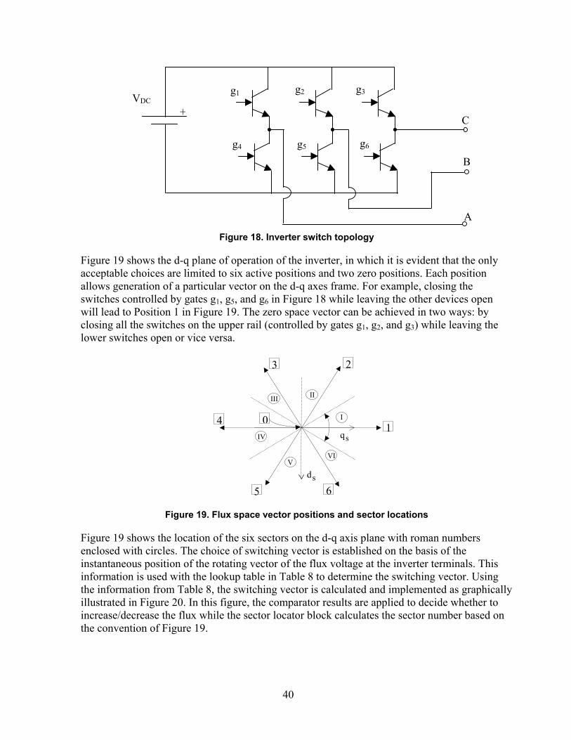
40
Figure 18. Inverter switch topology
Figure 19 shows the d-q plane of operation of the inverter, in which it is evident that the only acceptable choices are limited to six active positions and two zero positions. Each position allows generation of a particular vector on the d-q axes frame. For example, closing the switches controlled by gates g1, g5, and g6 in Figure 18 while leaving the other devices open will lead to Position 1 in Figure 19. The zero space vector can be achieved in two ways: by closing all the switches on the upper rail (controlled by gates g1, g2, and g3) while leaving the lower switches open or vice versa.
Figure 19. Flux space vector positions and sector locations
Figure 19 shows the location of the six sectors on the d-q axis plane with roman numbers enclosed with circles. The choice of switching vector is established on the basis of the instantaneous position of the rotating vector of the flux voltage at the inverter terminals. This information is used with the lookup table in Table 8 to determine the switching vector. Using the information from Table 8, the switching vector is calculated and implemented as graphically illustrated in Figure 20. In this figure, the comparator results are applied to decide whether to increase/decrease the flux while the sector locator block calculates the sector number based on the convention of Figure 19.
I
IIIII
IV
VVI
qs
ds
3 2
14
5 6
0
+C
B
A
g3
g6g5
g2g1
g4
VDC

41
The principle of operation of the inverter is to choose a zero vector if the angle of the voltage flux is to be decreased and to choose a vector from the lookup table in Table 8 if the angle needs to be increased. The knowledge of the sector number and whether the flux needs to be increased or decreased allows a selection of the switching vector. Each vector can be achieved at the terminals of the inverter by giving the appropriate gate pulses to control the switches.
Table 8. Choice of the Switching Vector
Sector Number
I II III IV V VI
Increase ΨV 2 3 4 5 6 1
Decrease ΨV 3 4 5 6 1 2
The gate pulse generator block shown in Figure 20 regulates the operation of the inverter. Within this block, the signals that control the power electronic devices of the inverter are generated. This block creates gate signals based on the information of flux of the voltage, which is described in detail in the next section. This flux of the voltage is a vector having magnitude and phase. The control continually generates the desired values, while the actual values are sought by a measuring system. Once the desired magnitude has been generated by the DR control, it is ensured that the inverter will give an output corresponding to the requested magnitude by sending the correct gate pulses to the power electronic devices. The actual voltage flux at the inverter terminals is measured and compared with the desired value, and based on the result, a choice is made on the switching sequence. Figure 20 shows how to generate the gate pulses for the inverter. The desired magnitude and angle for the voltage flux are compared with the actual magnitude and angle of the inverter voltage flux. Figure 20 also shows the gate pulse generator block of the inverter. The switching devices in the inverter have a rated maximum operating frequency. To enforce this constraint, the decision for the next switching sequence is made at a period corresponding to this maximum. It is possible that the next switching sequence is identical to the current one, and therefore no change in the switching vector is made during the transition. This ensures that power electronic switches are not switched faster than the maximum allowable frequency but may operate at lower frequencies.
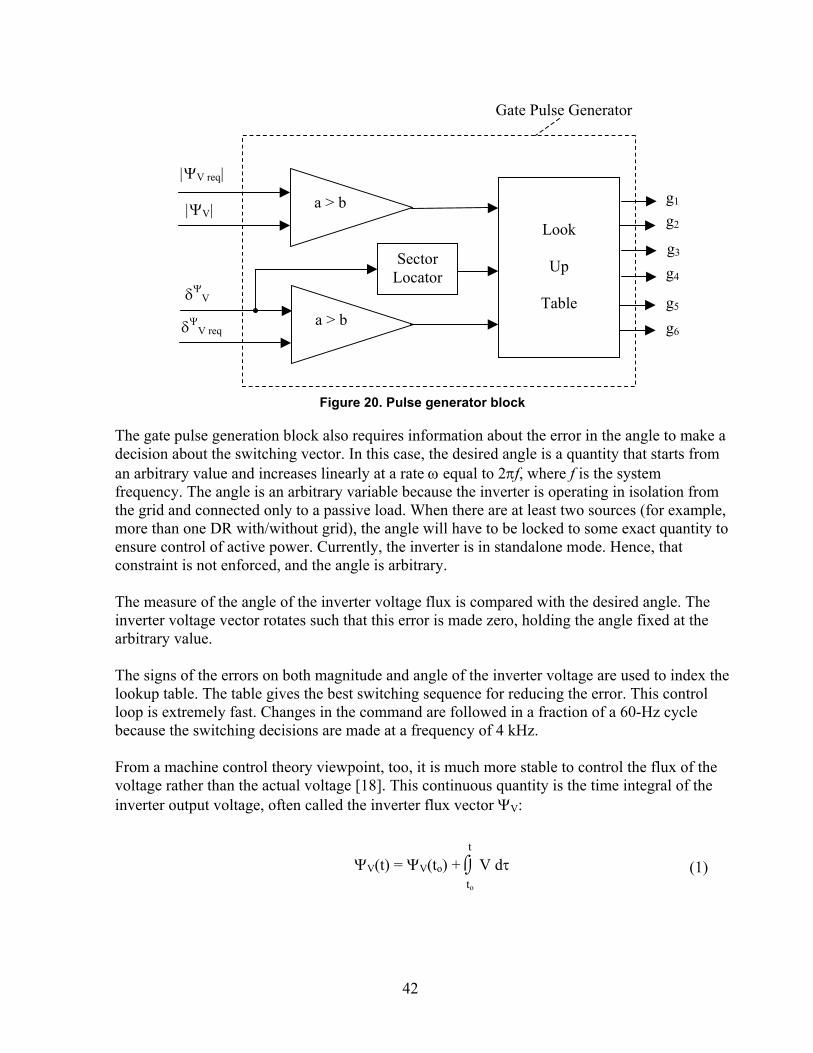
42
Figure 20. Pulse generator block
The gate pulse generation block also requires information about the error in the angle to make a decision about the switching vector. In this case, the desired angle is a quantity that starts from an arbitrary value and increases linearly at a rate ω equal to 2πf, where f is the system frequency. The angle is an arbitrary variable because the inverter is operating in isolation from the grid and connected only to a passive load. When there are at least two sources (for example, more than one DR with/without grid), the angle will have to be locked to some exact quantity to ensure control of active power. Currently, the inverter is in standalone mode. Hence, that constraint is not enforced, and the angle is arbitrary. The measure of the angle of the inverter voltage flux is compared with the desired angle. The inverter voltage vector rotates such that this error is made zero, holding the angle fixed at the arbitrary value. The signs of the errors on both magnitude and angle of the inverter voltage are used to index the lookup table. The table gives the best switching sequence for reducing the error. This control loop is extremely fast. Changes in the command are followed in a fraction of a 60-Hz cycle because the switching decisions are made at a frequency of 4 kHz. From a machine control theory viewpoint, too, it is much more stable to control the flux of the voltage rather than the actual voltage [18]. This continuous quantity is the time integral of the inverter output voltage, often called the inverter flux vector ΨV:
ΨV(t) = ΨV(to) + ⌡⌠to
t V dτ (1)
Sector Locator
Look
Up
Table
Gate Pulse Generator
a > b
a > b
g3
g1
g2
g4
g5
g6
|ΨV req|
|ΨV|
δΨV
δΨV req
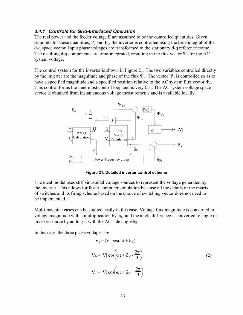
43
3.4.1 Controls for Grid-Interfaced Operation The real power and the feeder voltage E are assumed to be the controlled quantities. Given setpoints for these quantities, Po and Eo, the inverter is controlled using the time integral of the d-q space vector. Input phase voltages are transformed to the stationary d-q reference frame. The resulting d-q components are time-integrated, resulting in the flux vector Ψe for the AC system voltage. The control system for the inverter is shown in Figure 21. The two variables controlled directly by the inverter are the magnitude and phase of the flux Ψv. The vector Ψv is controlled so as to have a specified magnitude and a specified position relative to the AC system flux vector Ψe. This control forms the innermost control loop and is very fast. The AC system voltage space vector is obtained from instantaneous voltage measurements and is available locally.
Figure 21. Detailed inverter control scheme
The ideal model uses stiff sinusoidal voltage sources to represent the voltage generated by the inverter. This allows for faster computer simulation because all the details of the matrix of switches and its firing scheme based on the choice of switching vector does not need to be implemented. Multi-machine cases can be studied easily in this case. Voltage flux magnitude is converted to voltage magnitude with a multiplication by ωo, and the angle difference is converted to angle of inverter source by adding it with the AC side angle δE. In this case, the three phase voltages are:
Va = |V| cos(ωt + δV)
Vb = |V| cos
ωt + δV -
2π3 (2)
Vc = |V| cos
ωt + δV +
2π3
ωo
++
s
1
ω ω
P-I
P & Q Calculation
Flux Vector
Calculation
P
Q E
I
E
V
Power-Frequency droop
+
ωo Po
Eo ΨEo
ΨVo ΨE
|V|
δV
δPo
δE
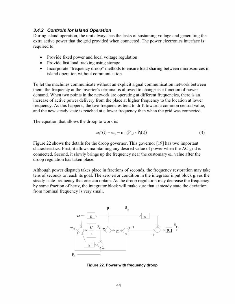
44
3.4.2 Controls for Island Operation During island operation, the unit always has the tasks of sustaining voltage and generating the extra active power that the grid provided when connected. The power electronics interface is required to:
• Provide fixed power and local voltage regulation • Provide fast load tracking using storage • Incorporate “frequency droop” methods to ensure load sharing between microsources in
island operation without communication. To let the machines communicate without an explicit signal communication network between them, the frequency at the inverter’s terminal is allowed to change as a function of power demand. When two points in the network are operating at different frequencies, there is an increase of active power delivery from the place at higher frequency to the location at lower frequency. As this happens, the two frequencies tend to drift toward a common central value, and the new steady state is reached at a lower frequency than when the grid was connected. The equation that allows the droop to work is:
ωi*(t) = ωo − mi (Pc,i - Pi(t)) (3) Figure 22 shows the details for the droop governor. This governor [19] has two important characteristics. First, it allows maintaining any desired value of power when the AC grid is connected. Second, it slowly brings up the frequency near the customary ωo value after the droop regulation has taken place. Although power dispatch takes place in fractions of seconds, the frequency restoration may take tens of seconds to reach its goal. The zero error condition in the integrator input block gives the steady-state frequency that one can obtain. As the droop regulation may decrease the frequency by some fraction of hertz, the integrator block will make sure that at steady state the deviation from nominal frequency is very small.
Figure 22. Power with frequency droop
ωo
s
k
s
"
k'
m P-I
δE
δP o
Po
P
ω *+ +
+
++ +
_
_
_Pc
ω s

45
The constant “m” in Figure 22 denotes the frequency droop without the frequency restoration loop active. Traditionally, the value of m was chosen in such a way that every machine picked up the extra quota of power proportionally to its own rating. Larger machines inject more power regardless of their operating point before the islanding. The proposed control behaves differently because new power is given in such a way as to cancel the power flow on some key branches of the network. This means that local demand is met by local generation, and there will be no flow of power in the transformers and in the cable that connects the factory with the warehouse and office. This goal is pursued to lower transmission losses in the system. As a consequence of this choice, the coefficient m depends on the local setpoint before islanding, Poi, and the new setpoint to be reached after the grid has failed, P1i:
mi = ωο - ωminPoi - P1i
(4)
Figure 22 gives the characteristic of the droop regulation when only two machines are present. DR2 operates at higher output than DR1. As the system enters island mode, the frequency will reduce. With the full load of the system, the new frequency will be ωmin. If there is a lighter load, the new frequency will be somewhere between ωo and ωmin. The slower frequency restoration loop will rigidly translate the characteristics upward until ω1 ≈ ωo.
Figure 23. P-ω droop characteristic
It is important that the power stay constant at the new dispatched level during the frequency restoration phase. The droop power control results in a single new steady-state point with a lower frequency ω1 at t = t1 along with a set of different power levels Pi(t1) for each power source. A control loop is used to uniformly bring the island system frequency near to ωo while holding the power levels of each source fixed at Pi(t1). The rate of changes of frequency for each source must also be held equal to ensure fixed power angles between sources. This basic condition implies:
dωidt =
dωjdt ∀ i,j (5)
P
ω
Po1 Po2
P11 P12
ωο
ω1 ωmin
46
From (3), assuming Pi(t) is constant for t ≥ t1, the rate of change of speed is:
dωidt = - mi
dPcidt (6)
Assuming again that Pi(t) is constant for t ≥ t1, it is possible to write:
ωi(t1) - ωi(t) = mi (Pci(t1) - Pci(t)) (7) Because the frequency restoration loop is much slower than the droop controller, it can be assumed that: Pci(t1) ≈ Poi (8) From the integral block of Figure 22:
dPcidt = ki" [ ](ωo - ωi) + ki' (Poi - Pci) (9)
Solving (6), (7), (8), and (9) yields:
dωidt = - mi ki"
(ωo - ωi) +
ki'mi
(Poi - Pci) (10)
It is required that the right side of (10) be equal for all sources or the terms miki” and ki’/mi be equal for all sources. This implies that gains i'k and i"k are dependent on the setpoints Poi and P1i, respectively, of each system. If a machine changes its setpoint, it doesn’t need to communicate to the other machines for this procedure to be successful. 3.5 Simulation Results In this section, the waveforms obtained from digital simulation of a two-inverter microgrid are presented. The real and reactive power sharing between the two DR as well as their voltage regulation operation are demonstrated. The digital simulation has been carried out in Electromagnetic Transients Program software. Data obtained from the simulation were plotted using the Matlab software package. Elaborate results in the form of time-domain waveforms and performance characteristics are illustrated. It is assumed that the microgrid is balanced in all three phases. To demonstrate the operation of the microgrid under changing load conditions, Load12 in the system illustrated in Figure 17 is assumed to be a variable one.
47
3.5.1 Island Mode of Operation The simulation waveforms for a step change in the three-phase balanced load between DR1 and DR2 (Load12) under island mode of operation (i.e., when the grid utility is disconnected) are displayed in figures 24 through 27. In the island mode of operation, the two DR provide all the energy requirements of the loads in the microgrid. The power flow across branches L1 and L2 are illustrated in Figure 24, in which the link between the grid utility transformer and DR1 is denoted by L1 and the link between the intermediate load (in the middle of the two DR) and DR2 is denoted by L2. As shown in Figure 24, because the DR is in island mode, the change in load demand between DR1 and DR2 (Load12) is accommodated by the two DR themselves (and not by the grid utility), per their power-frequency droop characteristics. This is also evident from the power outputs of each DR as demonstrated by Figure 25.
Rea
l pow
er (k
W)
t (s)
Figure 24. Real power across lines L1 and L2 for a step change in Load12 in island mode
The simulation results showing reactive power output of each DR for the same load change (i.e., Load12) are shown in Figure 26. The change in reactive power output is for regulating their terminal voltage. The waveforms illustrating terminal voltage variation with a step change in the load between DR1 and DR2 (Load12) are illustrated in Figure 27.
48
Rea
l pow
er (k
W)
t (s)
Figure 25. Real power outputs of DR1 and DR2 for a step change in Load12 in island mode
Rea
ctiv
e po
wer
(kV
ar)
t (s)
Figure 26. Reactive power outputs of DR1 and DR2 for a step change in Load12 in island mode
49
Term
inal
vol
tage
(kV
)
t (s)
Figure 27. Terminal voltages of DR1 and DR2 for a step change in Load12 in island mode
During standalone operation, the output power of the DR is not being controlled directly. This output value is determined by the power-frequency droop, ensuring that both units are injecting enough power to supply all the loads in the isolated microgrid. The simulation plots show that after increasing Load12, the power outputs of both the DR increase to match the new power requested. As soon as the new load is connected, the angles of the voltages in the network change. The DR interpret this change as an instantaneous change in the local value of the system frequency and activate the droop characteristic and ultimately ramp up their output power. The plots for power flowing in the feeders show there is no power flowing from the grid at all times because the measure in the section immediately preceding the first DR is zero. The power flowing in the section preceding the second unit decreases. This is because the second DR injects more power. Therefore, less power is requested from the feeder because no loads are changed in the segment of the microgrid behind the second unit. The reactive power changes because more current is flowing from unit one to the intermediate load. More losses are expected in that section, and the first unit has to provide more voltage support than before the load was changed. Because the power flow is decreased from the intermediate load to the second unit, lower voltage drops are expected, and the second unit has to provide less voltage support than when the grid is available. 3.5.2 Grid-Interfaced Mode of Operation The simulation waveforms for a step change in the three-phase balanced load between DR1 and DR2 (Load12) under grid-interfaced mode (i.e., when the grid utility is connected) are displayed in figures 28 through 31. In this mode, the energy requirements of the loads are shared among the DR and with the grid utility.
50
The power flow across branches L1 and L2 are illustrated in Figure 28. As explained earlier, the link between the grid utility transformer and DR1 is denoted by L1. The link between the intermediate load (in the middle of the two DR) and DR2 is denoted by L2. Figure 28 shows that, because the DR are in grid-interfaced mode, the change in load demand between DR1 and DR2 (Load12) is almost totally accommodated by the grid utility. The power-frequency droop characteristics of the grid utility are nearly flat. This is also evident from the power outputs of each DR as demonstrated by Figure 29.
Rea
l pow
er (k
W)
t (s)
Figure 28. Real power across lines L1 and L2 for a step change in Load12
in grid-interfaced mode
51
Rea
l pow
er (k
W)
t (s)
Figure 29. Real power outputs of DR1 and DR2 for a step change in Load12
in grid-interfaced mode
The simulation results showing reactive power output of each DR for a step change in load between DR1 and DR2 (Load12) are shown in Figure 30. The change in reactive power output is for regulating their terminal voltage by the controller action. The waveforms illustrating terminal voltage variation with a step change in the load between DR1 and DR2 (Load12) are illustrated in Figure 31. In grid-connected mode, the output power from the units will only have a transient change to settle back to their previous value. This transient change is because as soon as the load is inserted, the angle of the current flowing in the local grid changes, varying also the angle of the voltages at the regulated buses. The control of the DR corrects the angle of the voltage at the inverter terminals to compensate for the change in the angle at the regulated voltage bus. The grid ultimately is responsible for delivering the extra power needed to supply the new load. The line flow power plots show that the flow in the feeder immediately preceding the second DR is unchanged because no load change has taken place behind this section of the microgrid. The line flow plot for the section immediately preceding the first DR is changed, in the exact amount that the new load is requesting plus the extra losses in the feeders. The reactive power plots show that more reactive power is requested to sustain the voltage. This is because of the inductive nature of the load and the increased voltage drops across the feeders in the network because of larger currents.
52
Rea
ctiv
e po
wer
(kV
ar)
t (s)
Figure 30. Reactive power outputs of DR1 and DR2 for a step change in Load12
in grid-interfaced mode
Term
inal
vol
tage
(kV
)
t (s)
Figure 31. Terminal voltages of DR1 and DR2 for a step change in Load12
in grid-interfaced mode

53
Thus, while in grid-interfaced mode, both DR are regulating the power injected in the microgrid to a constant value. During stand-alone mode, the units switch from a constant output power to a power-frequency characteristic. This droop takes advantage of the instantaneous change in the microgrid frequency to ensure that all units adjust their output power to match the missing quota from the grid. The units also regulate bus voltage magnitude using a reactive power-voltage droop regardless of whether the grid connection exists.

54
4 Operation and Control of a Distributed Resource Under Imbalance
In the preceding chapter, the office-cum-warehouse facility was assumed to be a three-phase balanced load. However, in general, loads are imbalanced in a three-phase system. The power electronics equipment in a DR unit gives great flexibility of control. By using a PWM inverter in the DR, it is possible to provide UPS functionality, power quality improvement, and energy conversion simultaneously at a reasonable cost. The dynamic performance of the control can be improved with a multi-loop control strategy. A multi-loop control strategy is developed in this chapter to regulate the load bus voltage even under voltage imbalances. Furthermore, real and reactive power controllers are designed and analyzed to enable decentralized operation of the microgrid. The DR system shown in Figure 3 is illustrated by a detailed, three-phase circuit schematic in Figure 32. Each such unit is rated for supplying three-phase loads of 208 V at 60 Hz or single-phase loads of 120 V up to 15 kW three-phase (or one-third of 15 kW per phase) real power and equal reactive power. As shown in the figure, the DC bus can be modeled as a stiff DC source (VDC) because of adequate DC energy storage to manage load tracking [12]. The IGBTs and diodes in the figure are typically operated under a PWM strategy to synthesize sinusoidal output voltage waveforms of appropriate frequency and amplitude. The switching frequency components of the PWM output waveforms are filtered using a second-order low-pass filter of Lf and Cf. The filtered output voltage (VCf) is nominal 480-V line-line interfaced to the load through a reactor and three-phase transformer, whose equivalent series inductance is represented by Lt. The three-phase transformer illustrated in the figure is connected in a delta-wye configuration. This configuration allows for a three-phase, four-wire output, which enables simultaneous single-phase and three-phase loading as appropriate to meet application requirements. The circuit parameters of the DR inverter are listed in Table 9. It is possible to represent any complex three-phase load of 15 kW and 15 kVAr (maximum) in the form of generalized impedances (Za, Zb, and Zc) connected in Y as illustrated in the figure. The three-phase output voltage may also be interfaced to the utility and exchange power with another similar DR if necessary, so the net current flowing out of the terminals is labeled Itie. Another possibility is to connect the DR in Figure 32 to another DR and also the grid, in which case the net current will be the sum Igrid + Itie. For decentralized control of the microgrid, each of the DR in the microgrid is equipped with a regulator for voltage control at the local load bus and control of its real and reactive power output. This chapter describes the design of a regulator for the load bus voltage under imbalanced conditions. The voltage regulator design is carried out in stationary reference frame for three-phase complex space vector quantities using complex pole transfer functions. The magnitude and rotating angle of the complex reference voltage space vector are obtained from external real and reactive power regulators. These real and reactive power regulators are developed in a manner similar to that for conventional rotating machine generators.
55
VdcSA1
SA2
SB1
SB2
SC1
SC2
Idc
Lf Lf LfILfA ILfB ILfC
VNf
VCfA VCfB VCfCCf Cf Cf
VAp VBp VCp
VcnL
VbnL
VanL
VnL
TAC TBA TCBTa Tb Tc Z a
Z b Z c
ILda ILdb ILdc
ItieaItiebItiec
LtLt Lt ILtCILtCILtC
Figure 32. Power circuit schematic of the three-phase inverter
and its connection to three-phase loads
Table 9. Circuit Parameters of the DR
Parameter Value
VDC 750 V
VCf (nominal) 480 V
VxnL (nominal) 120 V
Lf 0.97 mH
Cf 30 µF
Lt 6.5 mH
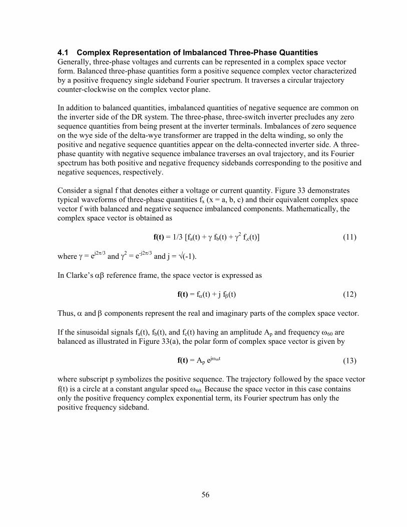
56
4.1 Complex Representation of Imbalanced Three-Phase Quantities Generally, three-phase voltages and currents can be represented in a complex space vector form. Balanced three-phase quantities form a positive sequence complex vector characterized by a positive frequency single sideband Fourier spectrum. It traverses a circular trajectory counter-clockwise on the complex vector plane. In addition to balanced quantities, imbalanced quantities of negative sequence are common on the inverter side of the DR system. The three-phase, three-switch inverter precludes any zero sequence quantities from being present at the inverter terminals. Imbalances of zero sequence on the wye side of the delta-wye transformer are trapped in the delta winding, so only the positive and negative sequence quantities appear on the delta-connected inverter side. A three-phase quantity with negative sequence imbalance traverses an oval trajectory, and its Fourier spectrum has both positive and negative frequency sidebands corresponding to the positive and negative sequences, respectively. Consider a signal f that denotes either a voltage or current quantity. Figure 33 demonstrates typical waveforms of three-phase quantities fx (x = a, b, c) and their equivalent complex space vector f with balanced and negative sequence imbalanced components. Mathematically, the complex space vector is obtained as f(t) = 1/3 [fa(t) + γ fb(t) + γ2 f,c(t)] (11) where γ = ej2π/3 and γ2 = e-j2π/3 and j = √(-1). In Clarke’s αβ reference frame, the space vector is expressed as f(t) = fα(t) + j fβ(t) (12) Thus, α and β components represent the real and imaginary parts of the complex space vector. If the sinusoidal signals fa(t), fb(t), and fc(t) having an amplitude Ap and frequency ω60 are balanced as illustrated in Figure 33(a), the polar form of complex space vector is given by f(t) = Ap ejω60t (13) where subscript p symbolizes the positive sequence. The trajectory followed by the space vector f(t) is a circle at a constant angular speed ω60. Because the space vector in this case contains only the positive frequency complex exponential term, its Fourier spectrum has only the positive frequency sideband.

57
Conversely, if the sinusoidal signals fa(t), fb(t), and fc(t) contain a negative sequence form of imbalance as shown in Figure 33(b), the complex space vector in polar form becomes f(t) = Ap ejω60t + An e-jω60t (14) where subscript n symbolizes the negative sequence, and Ap and An are the magnitudes of the positive and negative sequence quantities, respectively. The trajectory followed by the space vector f(t) is an ellipse with the major and minor axes of length (Ap + An) and (Ap – An), respectively. Because the space vector in this case contains complex exponential terms for both positive and negative frequencies, its Fourier spectrum has both positive and negative frequency sidebands. It should be noted that the spectral value at frequency +ω60 is the coefficient of the ejω60t term and that at frequency -ω60 it is the coefficient of the e-jω60t term in (14), respectively.
58
Figure 33. Complex vector mapping of three-phase AC sinusoidal signals
under (a) balanced and (b) negative sequence imbalanced conditions
In the DR system under consideration (Figure 32), the three-phase quantities of interest are the voltage across filter capacitor Cf and the currents through inductors Lf and Lt. These quantities can be represented in complex space vector form. Because the LfCfLt filter section of the system constitutes a three-phase, three-wire system, two phase variables are adequate to define the three-phase system. The filter capacitor voltages across lines ab and cb are combined to form a voltage space vector vCf(t). Likewise, filter inductor Lf and reactor Lt currents in phases a and c are represented as current space vectors iLf(t) and iLt(t), respectively.
(a) Balanced three-phase quantities
(b) Negative sequence imbalanced three-phase quantities
ω60
fAp
ω60−ω60α
β
f
Ap - An
ω60−ω60α
β
Ap + An
Fourier spectrum
frequency
frequency
Ap
Ap
Fourier spectrum
Space-vector trajectory
Space-vector trajectory
Three-phase quantities
0.01 0.02 0.03 0.04 0.05
5
0.01 0.02 0.03 0.04 0.05
5
Three-phase quantities
fx(t)
t
ab c
fx(t)
t
a b c

59
The voltage and current space vectors are determined as: vCf(t) = 1/3 [vCf,ab(t) + γ2 vCf,cb(t)] = vCf,α(t) + j vCf,β(t) (15) iLf(t) = 1/3 [(1 - γ) iLf,a(t) + (γ2 - γ) iLf,c(t)] = iLf,α(t) + j iLf,β(t) (16) iLt(t) = 1/3 [(1 - γ) iLt,a(t) + (γ2 - γ) iLt,c(t)] = iLt,α(t) + j iLt,β(t) (17) These complex vectors are conveniently used to develop the voltage and current controllers discussed later in this chapter. 4.2 Complex Transfer Functions In the previous section, it was noted that the Fourier spectra of the three-phase voltage and current space vectors are neither of equal magnitude nor symmetric about the frequency ω = 0. In contrast, the Fourier spectra of individual AC sinusoidal signals for each phase are of equal magnitude and symmetric about the frequency ω = 0. The sinusoidal quantities, Asin(ω60t) and Acos(ω60t), can be expressed as:
A cos(ω60t) = A
ejω
60t + e-jω
60t
2 (18)
and A sin(ω60t) = A
ejω
60t - e-jω
60t
2j (19)
The Fourier spectra of these quantities are illustrated in Figure 34.
(a) (b)
Figure 34. Fourier amplitude spectra of (a) cos(ω60t) and (b) sin(ω60t)
The signal processing of the AC sinusoidal real quantities is carried out using filters having transfer functions with real coefficients of s. Consider the low-pass filter transfer function:
Grlpf(s) =
1
1 +
s
ωc
(20)
0 ω60
A/2
−ω60
A/2
ω60
0−ω60
jA/2
-jA/2
ω ω
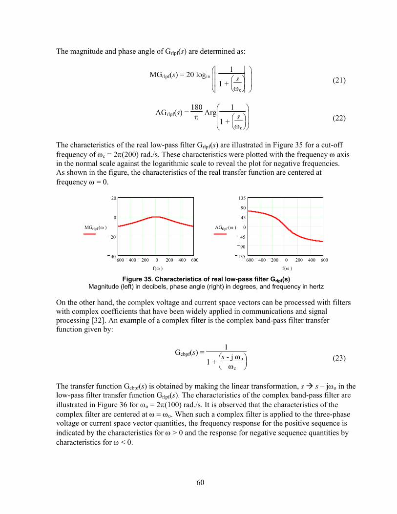
60
The magnitude and phase angle of Grlpf(s) are determined as:
MGrlpf(s) = 20 log10
1
1 +
s
ωc
(21)
AGrlpf(s) =
180π Arg
1
1 +
s
ωc
(22)
The characteristics of the real low-pass filter Grlpf(s) are illustrated in Figure 35 for a cut-off frequency of ωc = 2π(200) rad./s. These characteristics were plotted with the frequency ω axis in the normal scale against the logarithmic scale to reveal the plot for negative frequencies. As shown in the figure, the characteristics of the real transfer function are centered at frequency ω = 0.
600 400 200 0 200 400 60040
20
0
20
MGrlpf ω( )
f ω( )
600 400 200 0 200 400 600135
90
45
0
45
90
135
AGrlpf ω( )
f ω( )
Figure 35. Characteristics of real low-pass filter Grlpf(s) Magnitude (left) in decibels, phase angle (right) in degrees, and frequency in hertz
On the other hand, the complex voltage and current space vectors can be processed with filters with complex coefficients that have been widely applied in communications and signal processing [32]. An example of a complex filter is the complex band-pass filter transfer function given by:
Gcbpf(s) =
1
1 +
s - j ωo
ωc
(23)
The transfer function Gcbpf(s) is obtained by making the linear transformation, s s – jωo in the low-pass filter transfer function Grlpf(s). The characteristics of the complex band-pass filter are illustrated in Figure 36 for ωo = 2π(100) rad./s. It is observed that the characteristics of the complex filter are centered at ω = ωo. When such a complex filter is applied to the three-phase voltage or current space vector quantities, the frequency response for the positive sequence is indicated by the characteristics for ω > 0 and the response for negative sequence quantities by characteristics for ω < 0.
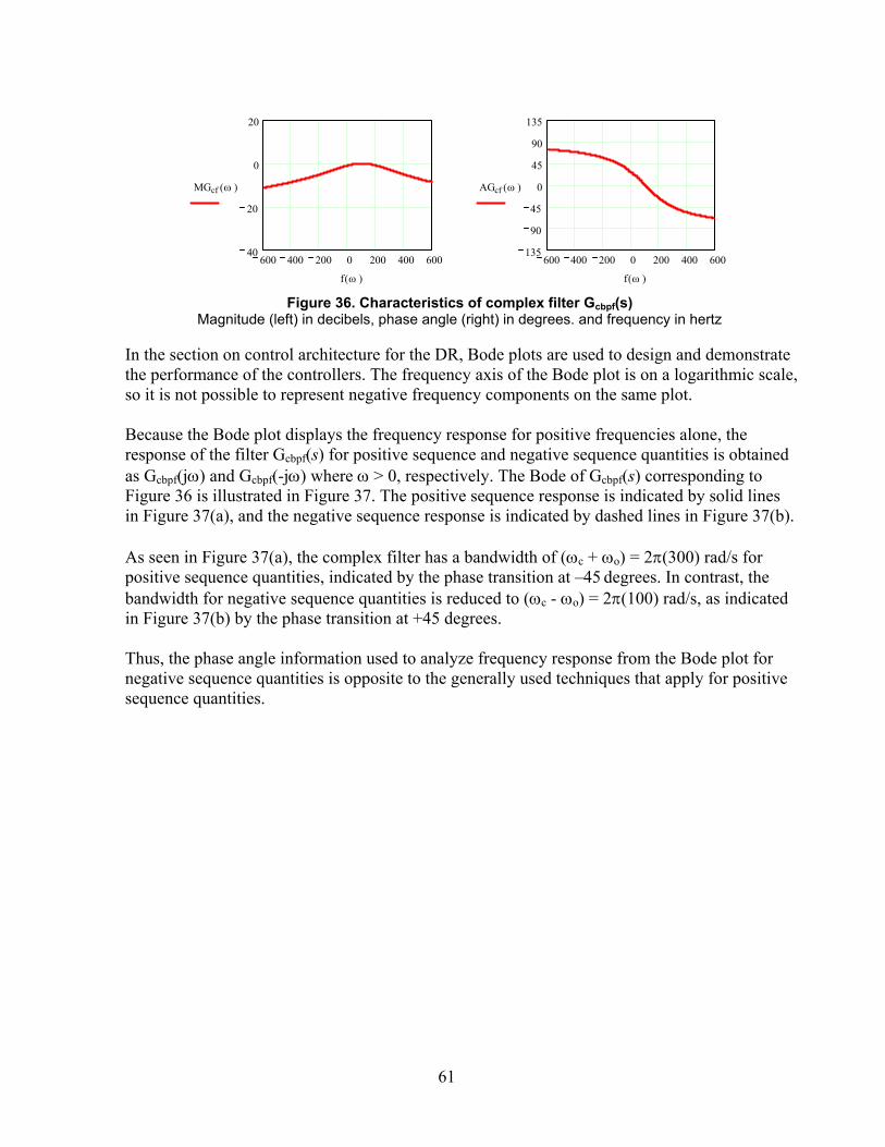
61
600 400 200 0 200 400 60040
20
0
20
MGcf ω( )
f ω( )
600 400 200 0 200 400 600135
90
45
0
45
90
135
AGcf ω( )
f ω( ) Figure 36. Characteristics of complex filter Gcbpf(s)
Magnitude (left) in decibels, phase angle (right) in degrees. and frequency in hertz
In the section on control architecture for the DR, Bode plots are used to design and demonstrate the performance of the controllers. The frequency axis of the Bode plot is on a logarithmic scale, so it is not possible to represent negative frequency components on the same plot. Because the Bode plot displays the frequency response for positive frequencies alone, the response of the filter Gcbpf(s) for positive sequence and negative sequence quantities is obtained as Gcbpf(jω) and Gcbpf(-jω) where ω > 0, respectively. The Bode of Gcbpf(s) corresponding to Figure 36 is illustrated in Figure 37. The positive sequence response is indicated by solid lines in Figure 37(a), and the negative sequence response is indicated by dashed lines in Figure 37(b). As seen in Figure 37(a), the complex filter has a bandwidth of (ωc + ωo) = 2π(300) rad/s for positive sequence quantities, indicated by the phase transition at –45 degrees. In contrast, the bandwidth for negative sequence quantities is reduced to (ωc - ωo) = 2π(100) rad/s, as indicated in Figure 37(b) by the phase transition at +45 degrees. Thus, the phase angle information used to analyze frequency response from the Bode plot for negative sequence quantities is opposite to the generally used techniques that apply for positive sequence quantities.
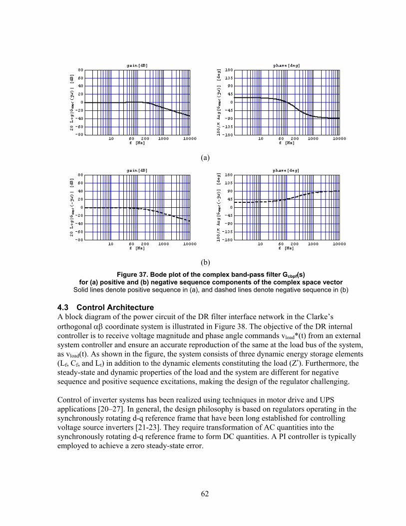
62
(a)
(b)
Figure 37. Bode plot of the complex band-pass filter Gcbpf(s) for (a) positive and (b) negative sequence components of the complex space vector
Solid lines denote positive sequence in (a), and dashed lines denote negative sequence in (b) 4.3 Control Architecture A block diagram of the power circuit of the DR filter interface network in the Clarke’s orthogonal αβ coordinate system is illustrated in Figure 38. The objective of the DR internal controller is to receive voltage magnitude and phase angle commands vload*(t) from an external system controller and ensure an accurate reproduction of the same at the load bus of the system, as vload(t). As shown in the figure, the system consists of three dynamic energy storage elements (Lf, Cf, and Lt) in addition to the dynamic elements constituting the load (Z’). Furthermore, the steady-state and dynamic properties of the load and the system are different for negative sequence and positive sequence excitations, making the design of the regulator challenging. Control of inverter systems has been realized using techniques in motor drive and UPS applications [20–27]. In general, the design philosophy is based on regulators operating in the synchronously rotating d-q reference frame that have been long established for controlling voltage source inverters [21-23]. They require transformation of AC quantities into the synchronously rotating d-q reference frame to form DC quantities. A PI controller is typically employed to achieve a zero steady-state error.

63
However, the transformation into the synchronous d-q reference frame under changing frequency environments such as utility applications requires a phase-locked loop to obtain unit vectors synchronized with the AC line [28]. Furthermore, conditions of imbalance in the system require implementation of separate controllers in positive and negative rotating reference frames that collectively supply the reference voltage of the inverter, thereby complicating system design [29]. An alternative method to realize high-performance current regulation with sinusoidal inputs without transformation to a rotating reference frame has been reported recently [26, 30]. In this section, a simpler approach is presented for multi-loop control of the inverter, and its performance under imbalanced and harmonic conditions is investigated. The multi-loop controller uses explicit design elements to ensure adequate performance for positive and negative sequence quantities in the system. Positive and negative sequence filters to isolate the two components from the measured quantities in real time, for use in the control, are developed. The proposed controller illustrated in Figure 39 uses a hierarchal approach to ensure adequate steady-state and dynamic performance with time-varying, three-phase sinusoidal command signals even in the presence of imbalanced operating conditions. At the outset, the feedback voltage regulator is built to regulate the filter capacitor voltage at the primary terminals of the transformer, vCf(t). This enables the feedback controller to be designed around a second-order system with reasonable performance attributes. The heart of the controller is a space vector modulator, which provides the duty ratio commands dinv(t) for various throws of the IGBT switches of the inverter, developed from the voltage command for the inverter vinv*(t). This controller incorporates a DC voltage feed-forward component to prevent any DC voltage disturbances from affecting the dynamic performance of the regulator. The space vector modulator operates at a switching frequency of 4 kHz. The realization of the space vector modulator is typically carried out using a digital signal processing system. At the next higher level in the controller is a current regulator that acts as an inner feedback loop and regulates the filter inductor Lf current. In the current loop design, capacitor voltage vCf(t) is added to the amplified error of the inductor Lf current to decouple the voltage vCf(t) and the current iLf(t). Because the filter inductor current is not the ultimate quantity of interest, the steady-state error performance is not critical and, hence, uses a simple proportional regulator. The command current for the inner current regulator loop itself iLf*(t) is derived from a filter capacitor Cf voltage regulator loop. The dynamic performance and stability of the closed-loop system is improved by adding the feed-forward current of inductor Lt [31]. The design of this regulator incorporates a controller that ensures accurate command following and disturbance rejection with sinusoidal inputs.
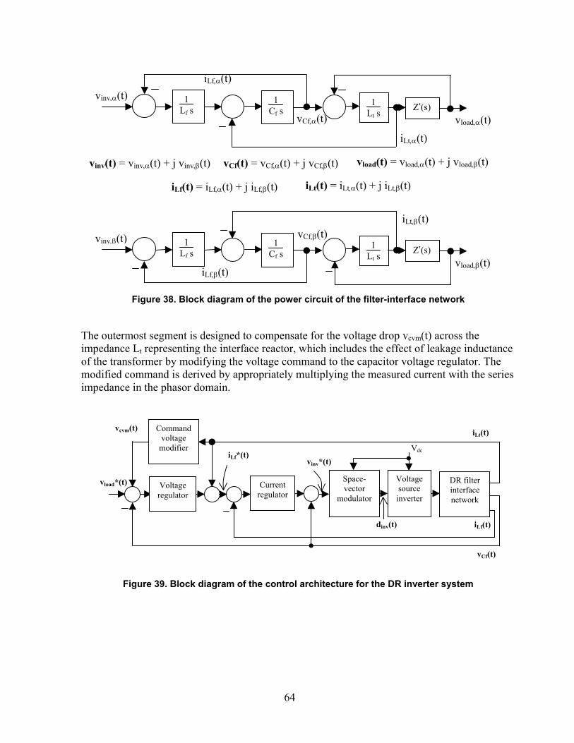
64
Figure 38. Block diagram of the power circuit of the filter-interface network
The outermost segment is designed to compensate for the voltage drop vcvm(t) across the impedance Lt representing the interface reactor, which includes the effect of leakage inductance of the transformer by modifying the voltage command to the capacitor voltage regulator. The modified command is derived by appropriately multiplying the measured current with the series impedance in the phasor domain.
Figure 39. Block diagram of the control architecture for the DR inverter system
iLf,α(t)
vinv(t) = vinv,α(t) + j vinv,β(t) vCf(t) = vCf,α(t) + j vCf,β(t)
1Lf s
vinv,α(t)
iLt,α(t)
1Cf s
vCf,α(t)1
Lt sZ’(s)
vload,α(t)
1Lf s
vinv,β(t)
iLt,β(t)
iLf,β(t)
1Cf s
vCf,β(t)1
Lt sZ’(s)
vload,β(t)
iLf(t) = iLf,α(t) + j iLf,β(t) iLt(t) = iLt,α(t) + j iLt,β(t)
vload(t) = vload,α(t) + j vload,β(t)
vinv*(t)
iLt(t)
Voltage regulator
iLf*(t)
vload*(t)
vCf(t)
Currentregulator
Space-vector
modulator
DR filter interface network
Command voltage
modifier
iLf(t)
Voltage source inverter
dinv(t)
vcvm(t)
Vdc
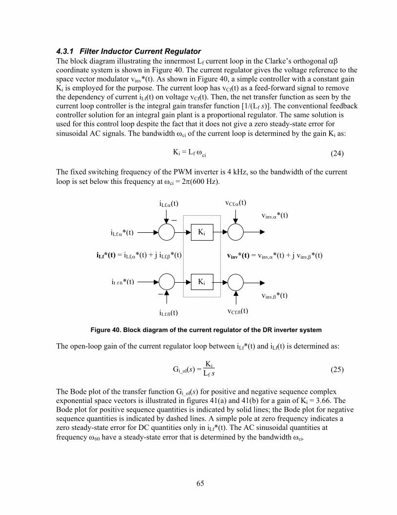
65
4.3.1 Filter Inductor Current Regulator The block diagram illustrating the innermost Lf current loop in the Clarke’s orthogonal αβ coordinate system is shown in Figure 40. The current regulator gives the voltage reference to the space vector modulator vinv*(t). As shown in Figure 40, a simple controller with a constant gain Ki is employed for the purpose. The current loop has vCf(t) as a feed-forward signal to remove the dependency of current iLf(t) on voltage vCf(t). Then, the net transfer function as seen by the current loop controller is the integral gain transfer function [1/(Lf s)]. The conventional feedback controller solution for an integral gain plant is a proportional regulator. The same solution is used for this control loop despite the fact that it does not give a zero steady-state error for sinusoidal AC signals. The bandwidth ωci of the current loop is determined by the gain Ki as: Ki = Lf ωci (24) The fixed switching frequency of the PWM inverter is 4 kHz, so the bandwidth of the current loop is set below this frequency at ωci = 2π(600 Hz).
Figure 40. Block diagram of the current regulator of the DR inverter system
The open-loop gain of the current regulator loop between iLf*(t) and iLf(t) is determined as:
Gi_ol(s) = Ki
Lf s (25)
The Bode plot of the transfer function Gi_ol(s) for positive and negative sequence complex exponential space vectors is illustrated in figures 41(a) and 41(b) for a gain of Ki = 3.66. The Bode plot for positive sequence quantities is indicated by solid lines; the Bode plot for negative sequence quantities is indicated by dashed lines. A simple pole at zero frequency indicates a zero steady-state error for DC quantities only in iLf*(t). The AC sinusoidal quantities at frequency ω60 have a steady-state error that is determined by the bandwidth ωci.
iLf*(t) = iLf,α*(t) + j iLf,β*(t)
iLf,α*(t) Ki
iLf,β*(t) Ki
vinv*(t) = vinv,α*(t) + j vinv,β*(t)
vinv,α*(t)
vinv,β*(t)
iLf,β(t)
iLf,α(t) vCf,α(t)
vCf,β(t)
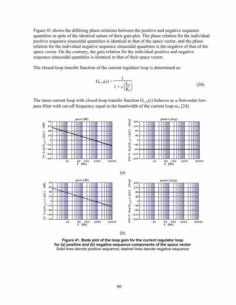
66
Figure 41 shows the differing phase relations between the positive and negative sequence quantities in spite of the identical nature of their gain plot. The phase relation for the individual positive sequence sinusoidal quantities is identical to that of the space vector, and the phase relation for the individual negative sequence sinusoidal quantities is the negative of that of the space vector. On the contrary, the gain relation for the individual positive and negative sequence sinusoidal quantities is identical to that of their space vector. The closed-loop transfer function of the current regulator loop is determined as:
Gi_cl(s) =
1
1 + s
Lf
Ki
(26)
The inner current loop with closed-loop transfer function Gi_cl(s) behaves as a first-order low-pass filter with cut-off frequency equal to the bandwidth of the current loop ωci [24].
(a)
(b)
Figure 41. Bode plot of the loop gain for the current regulator loop for (a) positive and (b) negative sequence components of the space vector Solid lines denote positive sequence; dashed lines denote negative sequence
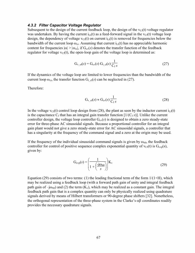
67
4.3.2 Filter Capacitor Voltage Regulator Subsequent to the design of the current feedback loop, the design of the vCf(t) voltage regulator was undertaken. By having the current iLt(t) as a feed-forward signal in the vCf(t) voltage loop design, the dependency of voltage vCf(t) on current iLt(t) is removed for frequencies below the bandwidth of the current loop ωci. Assuming that current iLt(t) has no appreciable harmonic content for frequencies |ω| > |ωci|, if Gcv(s) denotes the transfer function of the feedback regulator for voltage vCf(t), the open-loop gain of the voltage loop is determined as:
Gv_ol(s) = Gcv(s) Gi_cl(s) 1
Cf s (27)
If the dynamics of the voltage loop are limited to lower frequencies than the bandwidth of the current loop ωci, the transfer function Gi_cl(s) can be neglected in (27). Therefore:
Gv_ol(s) ≈ Gcv(s) 1
Cf s (28)
In the voltage vCf(t) control loop design from (28), the plant as seen by the inductor current iLf(t) is the capacitance Cf that has an integral gain transfer function [1/(Cf s)]. Unlike the current controller design, the voltage loop controller Gcv(s) is designed to obtain a zero steady-state error for three-phase AC sinusoidal signals. Because a proportional controller for an integral gain plant would not give a zero steady-state error for AC sinusoidal signals, a controller that has a singularity at the frequency of the command signal and a zero at the origin may be used. If the frequency of the individual sinusoidal command signals is given by ω60, the feedback controller for control of positive sequence complex exponential quantity of vCf(t) is Gcvp(s), given by:
Gcvp(s) =
1
1 +
-jω60
s
Kv (29)
Equation (29) consists of two terms: (1) the leading fractional term of the form 1/(1+H), which may be realized using a feedback loop (with a forward path gain of unity and integral feedback path gain of –jω60) and (2) the term (Kv), which may be realized as a constant gain. The integral feedback path gain that is a complex quantity can only be physically realized using quadrature signals derived by means of Hilbert transformers or 90-degree phase shifters [32]. Nonetheless, the orthogonal representation of the three-phase system in the Clarke’s αβ coordinates readily provides the necessary quadrature signals.
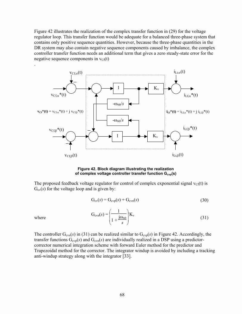
68
Figure 42 illustrates the realization of the complex transfer function in (29) for the voltage regulator loop. This transfer function would be adequate for a balanced three-phase system that contains only positive sequence quantities. However, because the three-phase quantities in the DR system may also contain negative sequence components caused by imbalance, the complex controller transfer function needs an additional term that gives a zero steady-state error for the negative sequence components in vCf(t) .
Figure 42. Block diagram illustrating the realization
of complex voltage controller transfer function Gcvp(s)
The proposed feedback voltage regulator for control of complex exponential signal vCf(t) is Gcv(s) for the voltage loop and is given by: Gcv(s) = Gcvp(s) + Gcvn(s) (30)
where Gcvn(s) =
1
1 + jω60
s
Kv (31)
The controller Gcvn(s) in (31) can be realized similar to Gcvp(s) in Figure 42. Accordingly, the transfer functions Gcvp(s) and Gcvn(s) are individually realized in a DSP using a predictor-corrector numerical integration scheme with forward Euler method for the predictor and Trapezoidal method for the corrector. The integrator windup is avoided by including a tracking anti-windup strategy along with the integrator [33].
vCf,α(t) iLt,α(t)
-ω60/s
1
vCf*(t) = vCf,α*(t) + j vCf,β*(t)
1
-ω60/s
Kv
Kv
iLf*(t) = iLf,α*(t) + j iLf,β*(t)
vCf,β*(t)
vCf,β(t)
vCf,α*(t)
iLt,β(t)
iLf,β*(t)
iLf,α*(t)
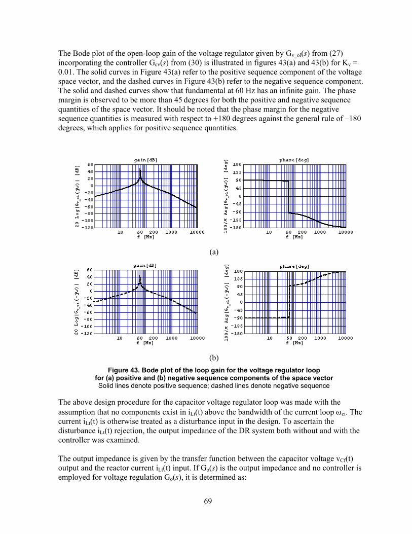
69
The Bode plot of the open-loop gain of the voltage regulator given by Gv_ol(s) from (27) incorporating the controller Gcv(s) from (30) is illustrated in figures 43(a) and 43(b) for Kv = 0.01. The solid curves in Figure 43(a) refer to the positive sequence component of the voltage space vector, and the dashed curves in Figure 43(b) refer to the negative sequence component. The solid and dashed curves show that fundamental at 60 Hz has an infinite gain. The phase margin is observed to be more than 45 degrees for both the positive and negative sequence quantities of the space vector. It should be noted that the phase margin for the negative sequence quantities is measured with respect to +180 degrees against the general rule of –180 degrees, which applies for positive sequence quantities.
(a)
(b)
Figure 43. Bode plot of the loop gain for the voltage regulator loop for (a) positive and (b) negative sequence components of the space vector Solid lines denote positive sequence; dashed lines denote negative sequence
The above design procedure for the capacitor voltage regulator loop was made with the assumption that no components exist in iLt(t) above the bandwidth of the current loop ωci. The current iLt(t) is otherwise treated as a disturbance input in the design. To ascertain the disturbance iLt(t) rejection, the output impedance of the DR system both without and with the controller was examined. The output impedance is given by the transfer function between the capacitor voltage vCf(t) output and the reactor current iLt(t) input. If Go(s) is the output impedance and no controller is employed for voltage regulation Go(s), it is determined as:
70
Go(s) =
-1
Cf s
1
1 + 1
Lf Cf s2 (32)
From (32), it is clear that the output impedance of the LfCf filter is maximum (infinity) at the corner frequency of the filter, (i.e., ω = ± 1/(LfCf) and is minimum at the frequency ω = 0). By contrast, the output impedance with the controller when vload*(t) is zero is given by:
Go(s)
Vload*(s) = 0 =
-1
Cf (s + ωci)
1
1 + 2 Kv ωci
Cf (s + ωci) (s2 + ω602)
(33)
The multi-loop controller improves the output impedance. The output impedance with the controller is minimum at frequencies ω = 0 and ω = ±ω60. This is because of the infinite gain of Gcv(s) at ω = ±ω60. Furthermore, there is no infinite gain at ω = ± 1/(LfCf). Thus, the parallel resonance of the LfCf filter is eliminated by the action of the multi-loop controller. The Bode plot of Go(s) without and with the controller is illustrated in figures 44(a) and 44(b). The response for positive sequence quantities is represented by solid lines; that for negative sequence quantities is represented by dashed lines. As seen in Figure 44, without the controller, the LfCf filter exhibits parallel resonance to iLt(t) at its corner frequency of 933 Hz, and the positive and negative sequence responses are matched. By employing the proportional controller with capacitor voltage vCf(t) feed-forward in the inner current loop, this parallel resonance is damped. Furthermore, use of the inductor current iLt(t) feed-forward in the outer voltage loop provides a low impedance for all frequencies well below the bandwidth of the current loop ωci. The voltage regulator having singularities at ω = ±ω60 ensures a transmission zero for positive and negative sequence components of iLt(t) complex space vector. This is indicated by a low gain at the fundamental frequency in the positive and negative sequence responses. Thus, the controller Gcv(s) provides good disturbance rejection in addition to command tracking for fundamental quantities.
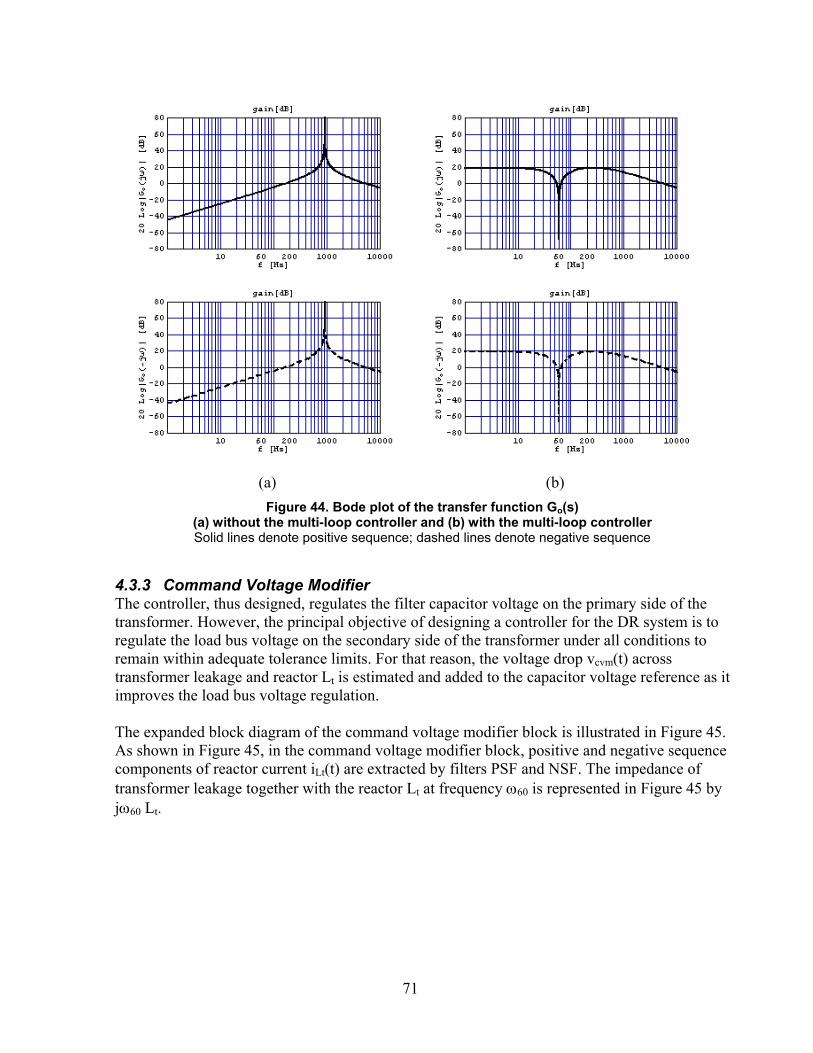
71
(a) (b)
Figure 44. Bode plot of the transfer function Go(s) (a) without the multi-loop controller and (b) with the multi-loop controller Solid lines denote positive sequence; dashed lines denote negative sequence
4.3.3 Command Voltage Modifier The controller, thus designed, regulates the filter capacitor voltage on the primary side of the transformer. However, the principal objective of designing a controller for the DR system is to regulate the load bus voltage on the secondary side of the transformer under all conditions to remain within adequate tolerance limits. For that reason, the voltage drop vcvm(t) across transformer leakage and reactor Lt is estimated and added to the capacitor voltage reference as it improves the load bus voltage regulation. The expanded block diagram of the command voltage modifier block is illustrated in Figure 45. As shown in Figure 45, in the command voltage modifier block, positive and negative sequence components of reactor current iLt(t) are extracted by filters PSF and NSF. The impedance of transformer leakage together with the reactor Lt at frequency ω60 is represented in Figure 45 by jω60 Lt.
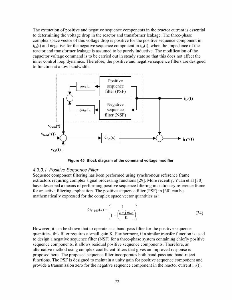
72
The extraction of positive and negative sequence components in the reactor current is essential to determining the voltage drop in the reactor and transformer leakage. The three-phase complex space vector of this voltage drop is positive for the positive sequence component in iLt(t) and negative for the negative sequence component in iLt(t), when the impedance of the reactor and transformer leakage is assumed to be purely inductive. The modification of the capacitor voltage command is to be carried out in steady state so that this does not affect the inner control loop dynamics. Therefore, the positive and negative sequence filters are designed to function at a low bandwidth.
Figure 45. Block diagram of the command voltage modifier
4.3.3.1 Positive Sequence Filter Sequence component filtering has been performed using synchronous reference frame extractors requiring complex signal processing functions [29]. More recently, Yuan et al [30] have described a means of performing positive sequence filtering in stationary reference frame for an active filtering application. The positive sequence filter (PSF) in [30] can be mathematically expressed for the complex space vector quantities as:
GY-PSF(s) =
1
1 +
s - j ω60
K (34)
However, it can be shown that to operate as a band-pass filter for the positive sequence quantities, this filter requires a small gain K. Furthermore, if a similar transfer function is used to design a negative sequence filter (NSF) for a three-phase system containing chiefly positive sequence components, it allows residual positive sequence components. Therefore, an alternative method using complex coefficient filters that gives an improved response is proposed here. The proposed sequence filter incorporates both band-pass and band-reject functions. The PSF is designed to maintain a unity gain for positive sequence component and provide a transmission zero for the negative sequence component in the reactor current iLt(t).
iLt(t)
Gcv(s) iLf*(t)vload*(t)
vCf(t)
Positive sequence
filter (PSF)
Negative sequence
filter (NSF) -jω60 Lt
vcvm(t)
jω60 Lt
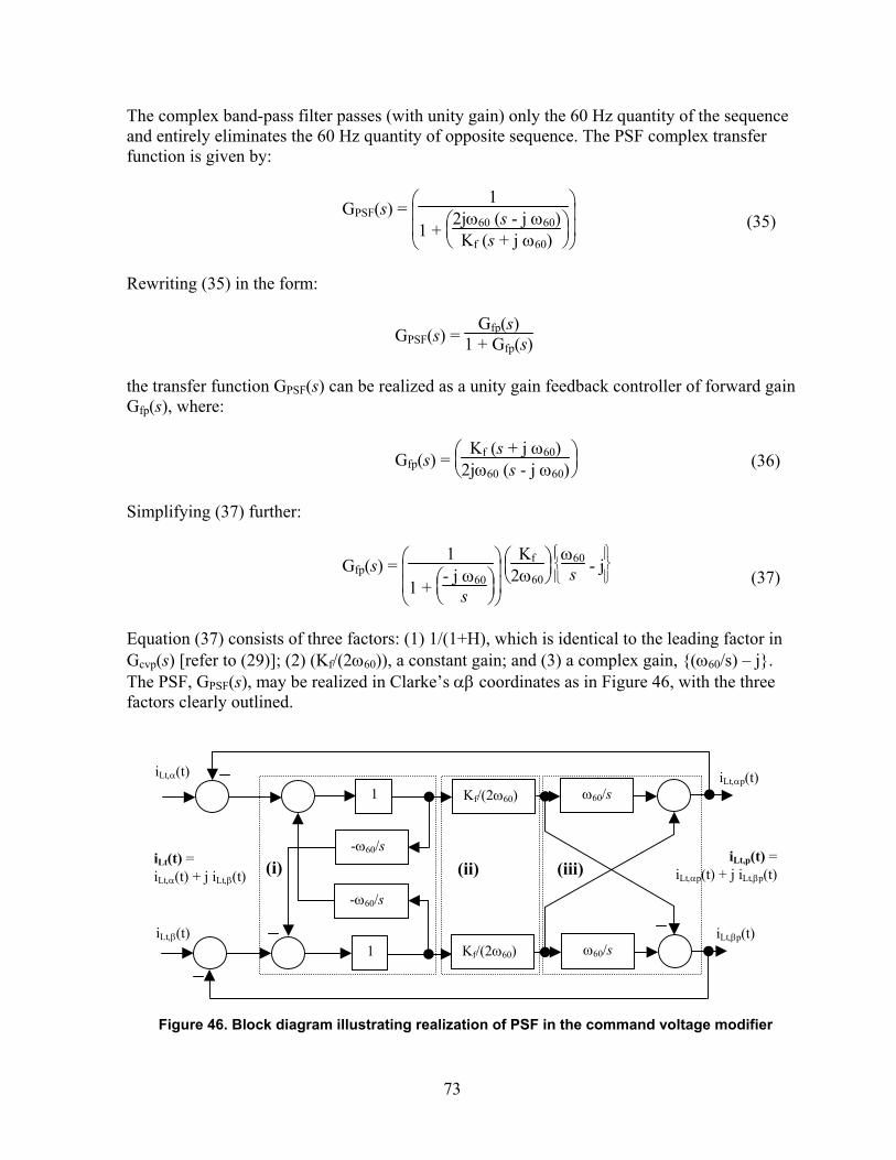
73
The complex band-pass filter passes (with unity gain) only the 60 Hz quantity of the sequence and entirely eliminates the 60 Hz quantity of opposite sequence. The PSF complex transfer function is given by:
GPSF(s) =
1
1 +
2jω60 (s - j ω60)
Kf (s + j ω60) (35)
Rewriting (35) in the form:
GPSF(s) = Gfp(s)
1 + Gfp(s)
the transfer function GPSF(s) can be realized as a unity gain feedback controller of forward gain Gfp(s), where:
Gfp(s) =
Kf (s + j ω60)
2jω60 (s - j ω60) (36)
Simplifying (37) further:
Gfp(s) =
1
1 +
- j ω60
s
Kf
2ω60
ω60
s - j (37)
Equation (37) consists of three factors: (1) 1/(1+H), which is identical to the leading factor in Gcvp(s) [refer to (29)]; (2) (Kf/(2ω60)), a constant gain; and (3) a complex gain, (ω60/s) – j. The PSF, GPSF(s), may be realized in Clarke’s αβ coordinates as in Figure 46, with the three factors clearly outlined.
Figure 46. Block diagram illustrating realization of PSF in the command voltage modifier
-ω60/s
1
1
-ω60/s
Kf/(2ω60)
iLt(t) = iLt,α(t) + j iLt,β(t)
iLt,β(t)
iLt,α(t) ω60/s
ω60/s
(i)
Kf/(2ω60)
(ii) (iii)
iLt,αp(t)
iLt,βp(t)
iLt,p(t) =iLt,αp(t) + j iLt,βp(t)
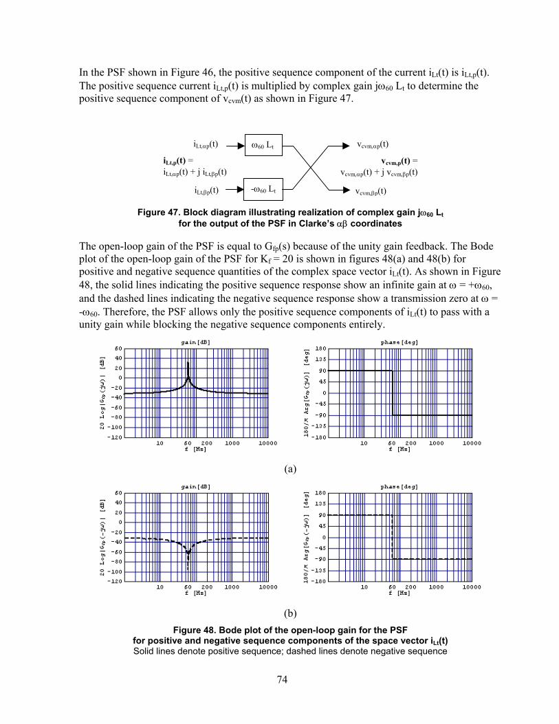
74
In the PSF shown in Figure 46, the positive sequence component of the current iLt(t) is iLt,p(t). The positive sequence current iLt,p(t) is multiplied by complex gain jω60 Lt to determine the positive sequence component of vcvm(t) as shown in Figure 47.
Figure 47. Block diagram illustrating realization of complex gain jω60 Lt
for the output of the PSF in Clarke’s αβ coordinates
The open-loop gain of the PSF is equal to Gfp(s) because of the unity gain feedback. The Bode plot of the open-loop gain of the PSF for Kf = 20 is shown in figures 48(a) and 48(b) for positive and negative sequence quantities of the complex space vector iLt(t). As shown in Figure 48, the solid lines indicating the positive sequence response show an infinite gain at ω = +ω60, and the dashed lines indicating the negative sequence response show a transmission zero at ω = -ω60. Therefore, the PSF allows only the positive sequence components of iLt(t) to pass with a unity gain while blocking the negative sequence components entirely.
(a)
(b)
Figure 48. Bode plot of the open-loop gain for the PSF for positive and negative sequence components of the space vector iLt(t) Solid lines denote positive sequence; dashed lines denote negative sequence
vcvm,p(t) =vcvm,αp(t) + j vcvm,βp(t)
vcvm,βp(t)
vcvm,αp(t)ω60 Lt
-ω60 Lt
iLt,p(t) = iLt,αp(t) + j iLt,βp(t)
iLt,αp(t)
iLt,βp(t)
75
4.3.3.2 Negative Sequence Filter Similar to the PSF, the negative sequence filter is designed to maintain unity gain for the negative sequence component while providing a transmission zero for the positive sequence component in iLt(t). The complex band-pass filter passes with unity gain only the 60 Hz quantity of the sequence and entirely eliminates the 60 Hz quantity of the opposite sequence. The NSF complex transfer function is given by:
GNSF(s) =
1
1 +
-2jω60 (s + j ω60)
Kf (s - j ω60) (38)
Rewriting (38) in the form:
GNSF(s) = Gfn(s)
1 + Gfn(s)
the transfer function GNSF(s) can be realized as a unity gain feedback controller of forward gain Gfn(s), where:
Gfn(s) =
Kf (s - j ω60)
-2jω60 (s + j ω60) (39)
Simplifying (39) further:
Gfn(s) =
1
1 + j ω60
s
Kf
2ω60
ω60
s + j (40)
Equation (40) consists of three factors: (1) 1/(1+H), which is identical to the leading factor in
Gcvn(s) [refer to (31)]; (2) (Kf/(2ω60)), a constant gain; and (3) a complex gain, (ω60/s) + j. The NSF, GNSF(s), may be realized in Clarke’s αβ coordinates as in
Figure 49, with the three factors clearly outlined.
76
Figure 49. Block diagram illustrating realization of NSF in the command voltage modifier
In the NSF shown in Figure 49, the negative sequence component of the current iLt(t) is iLt,n(t). The negative sequence current iLt,n(t) is multiplied by a complex gain -jω60 Lt to determine the negative sequence component of vcvm(t) as shown in Figure 50.
Figure 50. Block diagram illustrating realization of -jω60 Lt for the NSF in Clarke’s αβ coordinates
NSF is equivalent to the PSF with a switchover of the α and β terminals at the input and output. The open-loop gain of the NSF is equal to Gfp(s) because of the unity gain feedback. The Bode plot of the open-loop gain of the NSF for Kf = 20 is shown in figures 51(a) and 51(b) for positive and negative sequence quantities of the complex space vector iLt(t).
vcvm,n(t) =vcvm,αn(t) + j vcvm,βn(t)
vcvm,βn(t)
vcvm,αn(t)-ω60 Lt
ω60 Lt
iLt,n(t) = iLt,αn(t) + j iLt,βn(t)
iLt,αn(t)
iLt,βn(t)
ω60/s
1
1
ω60/s
Kf/(2ω60)
iLt(t) = iLt,α(t) + j iLt,β(t)
iLt,β(t)
iLt,α(t) ω60/s
ω60/s
(i)
Kf/(2ω60)
(ii) (iii)
iLt,αn(t)
iLt,βn(t)
iLt,n(t) =iLt,αn(t) + j iLt,βn(t)
77
(a)
(b)
Figure 51. Bode plot of the open-loop gain for the NSF for positive and negative sequence components of the space vector iLt(t) Solid lines denote positive sequence; dashed lines denote negative sequence
As shown in Figure 51, the solid lines indicating the positive sequence response show an infinite gain at ω = -ω60. The dashed lines indicating the negative sequence response show a transmission zero at ω = +ω60. Therefore, the NSF allows only the negative sequence components of iLt(t) to pass with a unity gain while blocking the positive sequence components entirely. The command voltage modifier output vcvm(t) is the sum of the estimated positive and negative sequence voltage drops across the leakage inductance of the transformer plus the reactor Lt. Accordingly, it is determined as: vcvm(t) = vcvm,p(t) + vcvm,n(t) (41) 4.3.4 Performance of the Voltage Regulator Against Imbalances In this section, the results of simulation studies conducted on the controllers for voltage regulation under imbalance are presented. The controllers tested include a filter inductor current regulator, a filter capacitor voltage regulator, and the command voltage modifier containing the positive and negative sequence filters. Digital simulation was carried out in Matlab SIMULINK™. The SimPowerSystems™ package was used to create various power quality events in the simulation.
78
Of the power quality disturbances, the low frequency electromagnetic phenomena of voltage imbalances, voltage sags, and harmonics are of interest in this project. Voltage imbalances at the load terminal are caused by load imbalances in the three phases because of unequal rms currents drawn from each phase of the voltage source. A typical case of unequal single-phase loads connected to the secondary terminals of the delta-wye transformer, when unregulated, is portrayed by the per-unit phasor plots in Figure 52. Voltage sags, on the other hand, are generated when a fault occurs on the network and draws high currents, thereby causing a large voltage drop. Finally, harmonics occur when nonlinear loads are connected in the system. The nonlinear loads draw non-sinusoidal currents for a sinusoidal supply voltage. Because these currents are periodic in nature, their Fourier components reveal the harmonic content in them.
Figure 52. Effect of imbalance (left) on the unregulated terminal voltage (right)
The effect of voltage imbalances or sags is a variation in the reactor current iLt. The performance of the controller is tested by simulating a disturbance that causes a variation in the reactor current iLt(t). In the multi-loop controller described earlier in this section, the inner current loop for iLf(t) is a simple proportional controller. The closed loop transfer function of the inner current loop is a low-pass filter of bandwidth ωci = 2π(600) rad./s. Figure 53 illustrates the response of the current controller. Noticeable is the fast response, though without a zero steady-state error between the reference and the measured quantities, as expected. The simple first-order low-pass filter transfer function does not give a zero steady-state error for AC sinusoidal quantities.
1 0.5 0 0.5 1
1
0.5
0.5
1
VanLVbnLVcnL
1.5 1 0.5 0 0.5 1 1.5
1.5
1
0.5
0.5
1
1.5
ILaILbILc
0.95∠-31 0.92∠-153 0.95∠88
0.67∠-76 1.3∠162 0.83∠43
79
0 0.05 0.1 0.15 0.2 0.25 0.3 0.35 0.4 0.45 0.5-100
-50
0
50
100
0 0.05 0.1 0.15 0.2 0.25 0.3 0.35 0.4 0.45 0.5
-100
-50
0
50
100
t (s)
i*Lf,ciLf,c
i*Lf,aiLf,a
Figure 53. Operation of the current control loop for iLf(t)
The voltage reference iLf*(t) is indicated by solid line; the response iLf(t) is indicated by a dashed line The performance of the voltage regulator for vCf(t) that consists of complex transfer functions for positive and negative sequence quantities is illustrated in Figure 54. Use of the complex controller gives a zero steady-state error for AC sinusoidal quantities of 60-Hz frequency of both positive and negative sequence. As shown in Figure 54, the voltages across lines ‘ab’ and ‘cb’ are not of identical amplitude. The overall objective of the multi-loop controller is to compensate the negative sequence imbalances and regulate the voltage at the sensitive load bus. An imbalanced capacitor voltage vCf(t) that cancels the voltage drop in the reactor Lt because of the current imbalance would provide a balanced voltage at the load bus.
80
0 0.05 0.1 0.15 0.2 0.25 0.3 0.35 0.4 0.45 0.5-1000
-500
0
500
1000
t (s)
0 0.05 0.1 0.15 0.2 0.25 0.3 0.35 0.4 0.45 0.5-1000
-500
0
500
1000v*Cf,ab
vCf,ab
v*Cf,cb
vCf,cb
Figure 54. Operation of the voltage control loop for vCf(t)
The voltage reference vCf*(t) is indicated by a solid line; the response vCf(t) is indicated by a dashed line
Figure 55 illustrates the line voltages obtained by subtracting the phase-neutral voltage in phase b from the two phase-neutral voltages in phases a and c. As shown in the figure, the two line voltages illustrate that the load bus voltage does not contain any negative sequence imbalances. Thus, the multi-loop controller regulates the load bus voltage even in the event of load imbalances of negative sequence.
81
0.25 0.3 0.35 0.4 0.45-300
-200
-100
0
100
200
300
t (s)
VanL - VbnLVcnL - VbnL
Figure 55. Line voltages at the load bus vxnL(t) - vbnL(t) (x = a, c),
illustrating that it does not contain negative sequence imbalance
Figures 56 and 57 illustrate the performance of the PSF and the NSF. The sequence filters are employed to extract the positive and negative sequence components of the reactor current iLt(t). Because the reactor inductance Lt is known, the positive and negative sequence voltage drops in it can be estimated. Thus, the command voltage for the capacitor voltage regulator is modified to compensate the negative sequence imbalance at the load bus. Figure 56 depicts the performance of the PSF in the Clarke’s αβ stationary reference frame. The top waveform in Figure 56 shows the α and β components of reactor current iLt(t), which show a negative sequence imbalance. The α and β components of the positive sequence filtered reactor current iLt p(t) are illustrated in the bottom waveform. From the figure, it is apparent that its α component leads the β component by 90 degrees. Accordingly, the space vector iLt p(t) contains only positive frequency complex exponential quantities (i.e., has only the positive frequency sideband in its Fourier spectrum).
82
0 0.05 0.1 0.15 0.2 0.25 0.3 0.35 0.4 0.45 0.5-150
-100
-50
0
50
100
150
0 0.05 0.1 0.15 0.2 0.25 0.3 0.35 0.4 0.45 0.5-150
-100
-50
0
50
100
150
t (s)
iLt,α piLt,β p
iLt,αiLt,β
Figure 56. Performance of the PSF on the reactor current iLt(t)
Figure 57 demonstrates the performance of the NSF in the Charke’s αβ stationary reference frame. The top waveform in Figure 57 shows the α and β components of reactor current iLt(t), which show a negative sequence imbalance. The α and β components of the negative sequence filtered reactor current iLt n(t) are illustrated in the bottom waveform. From the figure, it is apparent that its α component lags the β component by 90 degrees. Accordingly, the space vector iLt n(t) contains only negative frequency complex exponential quantities (i.e., has only the negative frequency sideband in its Fourier spectrum).
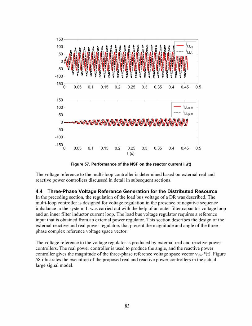
83
0 0.05 0.1 0.15 0.2 0.25 0.3 0.35 0.4 0.45 0.5-150
-100
-50
0
50
100
150
0 0.05 0.1 0.15 0.2 0.25 0.3 0.35 0.4 0.45 0.5-150
-100
-50
0
50
100
150
t (s)
iLt,α niLt,β n
iLt,αiLt,β
Figure 57. Performance of the NSF on the reactor current iLt(t)
The voltage reference to the multi-loop controller is determined based on external real and reactive power controllers discussed in detail in subsequent sections. 4.4 Three-Phase Voltage Reference Generation for the Distributed Resource In the preceding section, the regulation of the load bus voltage of a DR was described. The multi-loop controller is designed for voltage regulation in the presence of negative sequence imbalance in the system. It was carried out with the help of an outer filter capacitor voltage loop and an inner filter inductor current loop. The load bus voltage regulator requires a reference input that is obtained from an external power regulator. This section describes the design of the external reactive and real power regulators that present the magnitude and angle of the three-phase complex reference voltage space vector. The voltage reference to the voltage regulator is produced by external real and reactive power controllers. The real power controller is used to produce the angle, and the reactive power controller gives the magnitude of the three-phase reference voltage space vector vload*(t). Figure 58 illustrates the execution of the proposed real and reactive power controllers in the actual large signal model.

84
The power regulators for the DR in a microgrid are designed to offer the features of controlled power sharing and dispatchability. The basic control input for the reactive power controller is the load reactive power setpoint (in large signal) designated as QL-ref. A change in QL-ref causes a change in the voltage magnitude Vload that is later restored by the voltage regulator (in the voltage restoration loop of the reactive power-voltage controller) to near its nominal value. Likewise, the basic control input for the real power controller is the load real power setpoint (in large signal) designated as PL-ref. A change in PL-ref causes a change in the frequency that is later restored by the frequency governor (in the frequency restoration loop of the real power-frequency controller) to near its nominal value. Saturation limits are set in the regulators that are dependent on the maximum allowable voltage and frequency tolerances of sensitive loads. As shown in Figure 58, constant terms Vo and ωo [i.e., the nominal voltage (magnitude) and frequency] are added to the power regulator outputs in the reactive and real power controllers. Additional terms (Verr and ωerrt) are used for synchronization purposes at the time of shifting from standalone to grid-interfaced mode of operation. These refer to the errors in the magnitude and running angle of the grid terminal voltage from their nominal values, as reflected to the primary side of the ∆-Y transformer. The outputs of the external controllers are the magnitude Vload and running angle ωt of the voltage space vector vload(t). The individual line-line voltage references are determined by transforming the voltage space vector to the stationary three-phase coordinate system.
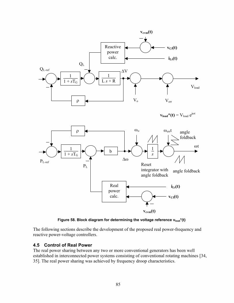
85
Figure 58. Block diagram for determining the voltage reference vload*(t)
The following sections describe the development of the proposed real power-frequency and reactive power-voltage controllers. 4.5 Control of Real Power The real power sharing between any two or more conventional generators has been well established in interconnected power systems consisting of conventional rotating machines [34, 35]. The real power sharing was achieved by frequency droop characteristics.
QL-ref QL
∆V
ρ
1L s + R
Vo Verr
Vload
vload*(t) = Vload ejωt
Reactive power calc.
vCf(t)
iLt(t)
vcvm(t)
PL-ref PL
∆ω
ρ
11 + sTG
b 1s
ωo ωerrt
Reset integrator with angle foldback
ωt
angle foldback
angle foldback
Real power calc.
vcvm(t)
vCf(t)
iLt(t)
11 + sTG
86
At the beginning, the control of power generation in the conventional rotating machine type generators is investigated. Subsequently, because the power sharing requirements of a microgrid are to some extent similar to those of a distributed UPS proposed by Chandorkar [36], the real power control of distributed UPS as presented in [36] is discussed before generation control in a microgrid. The demands of a microgrid are discussed, and a generation controller meeting those demands is presented. 4.5.1 Generation Control in a Two-Machine Interconnected Power System Power sharing in an interconnected power system is made possible by real power-frequency droop characteristics. The frequency/speed droop in a generator occurs when a change in load demand has been initially provided for by the inertia of the rotating mass and there is a delay in the response of the prime mover to accommodate the change in load. Governors are employed to allow the controller to detect the change in the machine speed and thereby vary the valve input of the prime mover. There are two forms of governing in a power system: generator governing and load governing [35]. When a load change occurs in the power system, generator governing refers to the speed/frequency droop in a machine and the subsequent action of the speed governor to raise the power input to the prime mover of the machine to restore the machine speed/frequency to near its nominal value. For a brief duration, the machine is able to support the load change by the stored kinetic energy of the rotating mass. On the other hand, a large percentage of loads, such as motor loads, draw a varied amount of real power proportionate to the supply frequency. Accordingly, when a load increase causes a decrease in machine speed, there is a decrease in the supply frequency, which eventually results in a net decrease in the load. This self-governing attribute of a rotating machine generator makes paralleling generators possible. The analysis of generation control is made with the deviation values from nominal/steady-state quantities. The deviations from the steady-state quantities are indicated by a ∆. Consider a single generator that is connected to a local load. The generator modeling is made by means of the relationship among mechanical power, electrical power, and speed change [34]. If M denotes the angular momentum of the machine in watts per radian per second and s is the Laplace transform variable, this relation is obtained as: ∆PM – ∆PE = M s ∆ω (42) where ∆PM and ∆PE are the net changes in mechanical and electrical powers of the machine. The electrical power is equal to the power consumed by the loads. The loads in a power system can be categorized broadly as those that are frequency-independent and those that are sensitive to frequency. Frequency-independent loads are mainly resistive loads. In contrast, motor loads when operating with variable power-frequency characteristics constitute frequency-dependent loads and contribute to load governing in the machine. It is well known that motors constitute the majority of loads in a power system.
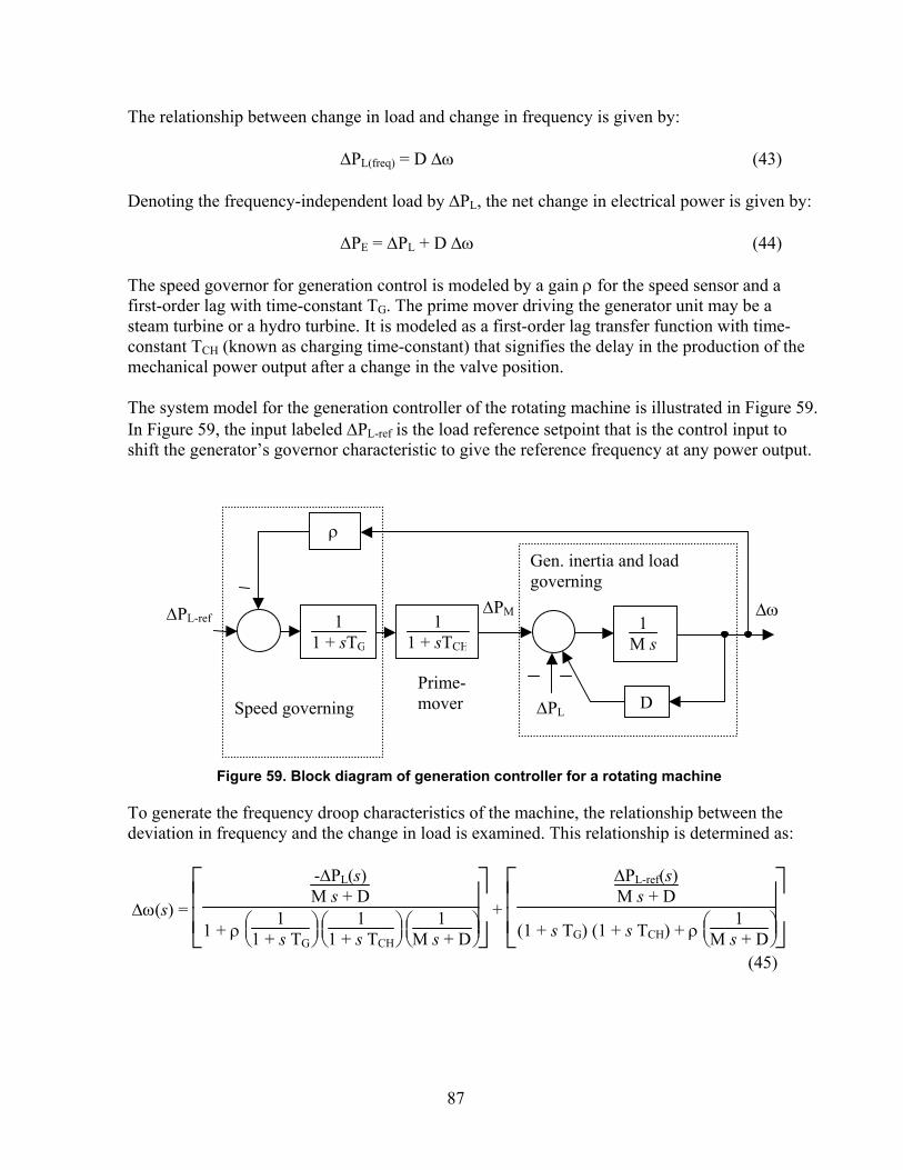
87
The relationship between change in load and change in frequency is given by: ∆PL(freq) = D ∆ω (43) Denoting the frequency-independent load by ∆PL, the net change in electrical power is given by: ∆PE = ∆PL + D ∆ω (44) The speed governor for generation control is modeled by a gain ρ for the speed sensor and a first-order lag with time-constant TG. The prime mover driving the generator unit may be a steam turbine or a hydro turbine. It is modeled as a first-order lag transfer function with time-constant TCH (known as charging time-constant) that signifies the delay in the production of the mechanical power output after a change in the valve position. The system model for the generation controller of the rotating machine is illustrated in Figure 59. In Figure 59, the input labeled ∆PL-ref is the load reference setpoint that is the control input to shift the generator’s governor characteristic to give the reference frequency at any power output.
Figure 59. Block diagram of generation controller for a rotating machine
To generate the frequency droop characteristics of the machine, the relationship between the deviation in frequency and the change in load is examined. This relationship is determined as:
∆ω(s) =
-∆PL(s)M s + D
1 + ρ
1
1 + s TG
1
1 + s TCH
1
M s + D
+
∆PL-ref(s)M s + D
(1 + s TG) (1 + s TCH) + ρ
1
M s + D (45)
1
M s
D
Gen. inertia and load governing
∆PM
∆PL
∆ω
ρ
11 + sTG
11 + sTCH
Speed governing
∆PL-ref
Prime-mover
88
The steady-state deviation in speed response is obtained by setting s = 0 in (45). The steady-state change in speed is obtained as:
∆ω = -∆PL
D + ρ + ∆PL-ref
D + ρ (46)
Because the load demand is supplied by the generator, the change in load demand is equal to the change in generator output denoted by ∆PG (i.e., ∆PG = ∆PL + D ∆ω). Then, (46) can be rewritten as:
∆ω = -∆PG
ρ + ∆PL-ref
ρ (47)
Equation (47) represents a straight line and can be graphically represented as shown in Figure 60(a). As shown in the figure, the straight line can be shifted along the ∆PG axis by varying ∆PL-ref. The same curves are displayed in Figure 60(b) for the actual speed ω and power output PG variables. Representing the nominal values of the quantities by a subscript “o,” the actual quantities are determined as: PG = PGo + ∆PG (48) and ω = ωo + ∆ω (49) Thus, Figure 60(b) characterizes the steady-state frequency droop feature of this generator. As shown in Figure 60(b), the actual quantity corresponding to the load reference setpoint is PL_ref. The value of PL_ref corresponding to a load reference setpoint of zero is PL_ref = PLo (where PLo = PGo). A positive value of load reference setpoint would refer to PL_ref > PLo and a negative value to PL_ref < PLo. By changing PL_ref, the controller can be set to give nominal frequency at any desired load condition.
Figure 60. Steady-state frequency droop of the generator
(a) Deviation quantities and (b) actual quantities
PL_ref = 0
PL_ref = PLo PL_ref = 2PLo
1.0 p.u. 2.0 p.u.
ωo
ω
PG 0
Slope = -(ρ)-1
∆PL-ref > 0
∆PL-ref < 0
∆ω
∆PG
Slope = -(ρ)-1
∆PL-ref = 0
(b)(a)
89
For two such generators connected by a tie line, the power flow through the tie line from one unit to the other is illustrated by Figure 61. As shown in the figure, the system has two buses, with each bus having a generator and a load. The generators at buses 1 and 2 are labeled Gen 1 and Gen 2, respectively. Likewise, the loads at buses 1 and 2 are labeled Load 1 and Load 2, respectively. The terminal voltages of the two generators are V1 ∠δ1 and V2 ∠δ2. By denoting the generated power and the load power as PG and PL, the real power flow through the tie line Ptie from Bus 1 to Bus 2 is given by: PG1 – PL1 = - PG2 + PL2 = Ptie (50) If the tie line connecting the two generators is of inductive reactance Xtie (in pu), the tie-line power Ptie (in pu) is determined as:
Ptie = V1 V2Xtie
sin(δ12) (51)
where δ12 = δ1 - δ2 (in rad).
Figure 61. Single-line diagram of real power flow
of an interconnected power system consisting of two generators
Assuming that δ12 is very small, sin(δ12) ≈ δ12 (52) Substituting (46) in (45),
Ptie = V1 V2Xtie
δ12 (53)
PG2 PG1 Ptie
PL1 PL2
Xtie
Tie-line
Gen 1 Gen 2
Load 1 Load 2
V1 ∠δ1 V2 ∠δ2
1 2
90
Denoting the steady-state quantities by a subscript “o,” the steady-state power flow through the tie line is given by:
Ptie o = V1o V2o
Xtie δ12 o (54)
At steady state, the generators operate at the common system frequency ω1o = ωo and ω2o = ωo. Consider small deviations in the quantities from their nominal/steady-state values. Designating the deviations by a ∆ and recognizing the fact that the deviations in the voltages do not effect the real power flow appreciably:
Ptie o + ∆Ptie ≈ V1o V2o
Xtie (δ12 o + ∆δ12) (55)
From (54) and (55):
∆Ptie = V1o V2o
Xtie ∆δ12 (56)
The change in the relative phase angle ∆δ12 is possible because of a momentary variation in the frequencies of the two generators before settling at a steady state. Denoting the actual frequencies of Gen 1 and Gen 2 as ω1 (in pu) and ω2 (in pu) where: ω1 = ωo + ∆ω1 (57) and ω2 = ωo + ∆ω2 (58) where ωo denotes the nominal system frequency in pu. The change in relative phase angle ∆δ12 because of the momentary change in the individual frequencies is determined as:
∆δ12 = ωbase ⌡⌠
(∆ω1 - ∆ω2)dt (59)
where ωbase is the base speed of the machine (in rad/s), the relative phase angle ∆δ12 is expressed in radian, and the frequencies ∆ω1 and ∆ω2 are expressed in pu. At the new steady-state condition, ∆ω1 = ∆ω2, and therefore, ∆ω1 - ∆ω2 = 0.
91
Substituting (59) in (56):
∆Ptie = ωbase V1o V2o
Xtie ⌡⌠
(∆ω1 - ∆ω2)dt (60)
Assuming that the nominal voltages are of 1.0 pu, the change in tie-line power is simplified as:
∆Ptie (s) = Ts ( )∆ω1 - ∆ω2 (61)
where T = 377/Xtie (in pu) for a 60-Hz system. The block diagram illustrating the power frequency relation in the interconnected power system is shown in Figure 62. The power flow through the tie line will appear as a positive load to one generator and an equal but negative load to the other. The direction of power flow is determined by the relative phase angle, which is, in turn, a function of the relative speed deviation between the two units.
Figure 62. Block diagram of the governor control for an
interconnected power system consisting of two generators
∆PM1
∆PL1
∆ω111 + sTG1
∆PM2
∆PL2
11 + sTCH2
1M1s + D1
Ts
∆ω2
11 + sTCH1
11 + sTG2
1M2s + D2
∆Ptie
ρ2
∆PL2-ref
∆PL1-ref
ρ1
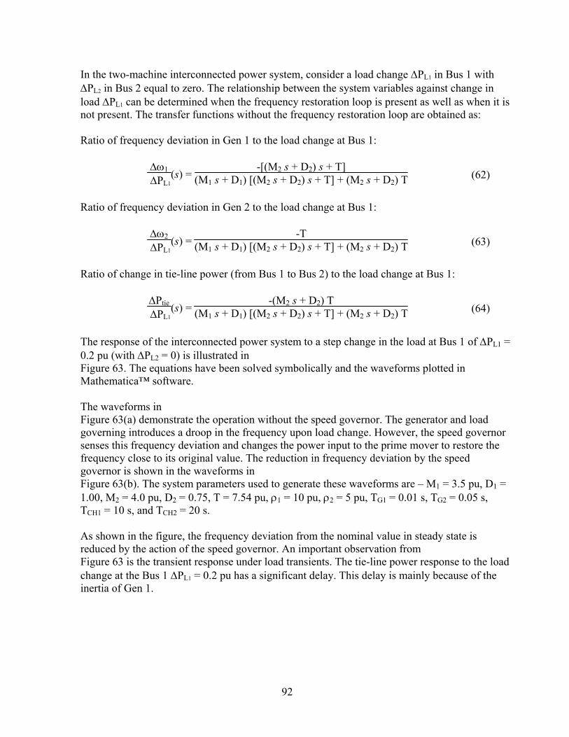
92
In the two-machine interconnected power system, consider a load change ∆PL1 in Bus 1 with ∆PL2 in Bus 2 equal to zero. The relationship between the system variables against change in load ∆PL1 can be determined when the frequency restoration loop is present as well as when it is not present. The transfer functions without the frequency restoration loop are obtained as: Ratio of frequency deviation in Gen 1 to the load change at Bus 1:
∆ω1
∆PL1(s) =
-[(M2 s + D2) s + T](M1 s + D1) [(M2 s + D2) s + T] + (M2 s + D2) T (62)
Ratio of frequency deviation in Gen 2 to the load change at Bus 1:
∆ω2
∆PL1(s) =
-T(M1 s + D1) [(M2 s + D2) s + T] + (M2 s + D2) T (63)
Ratio of change in tie-line power (from Bus 1 to Bus 2) to the load change at Bus 1:
∆Ptie
∆PL1(s) =
-(M2 s + D2) T(M1 s + D1) [(M2 s + D2) s + T] + (M2 s + D2) T (64)
The response of the interconnected power system to a step change in the load at Bus 1 of ∆PL1 = 0.2 pu (with ∆PL2 = 0) is illustrated in Figure 63. The equations have been solved symbolically and the waveforms plotted in Mathematica™ software. The waveforms in Figure 63(a) demonstrate the operation without the speed governor. The generator and load governing introduces a droop in the frequency upon load change. However, the speed governor senses this frequency deviation and changes the power input to the prime mover to restore the frequency close to its original value. The reduction in frequency deviation by the speed governor is shown in the waveforms in Figure 63(b). The system parameters used to generate these waveforms are – M1 = 3.5 pu, D1 = 1.00, M2 = 4.0 pu, D2 = 0.75, T = 7.54 pu, ρ1 = 10 pu, ρ2 = 5 pu, TG1 = 0.01 s, TG2 = 0.05 s, TCH1 = 10 s, and TCH2 = 20 s. As shown in the figure, the frequency deviation from the nominal value in steady state is reduced by the action of the speed governor. An important observation from Figure 63 is the transient response under load transients. The tie-line power response to the load change at the Bus 1 ∆PL1 = 0.2 pu has a significant delay. This delay is mainly because of the inertia of Gen 1.
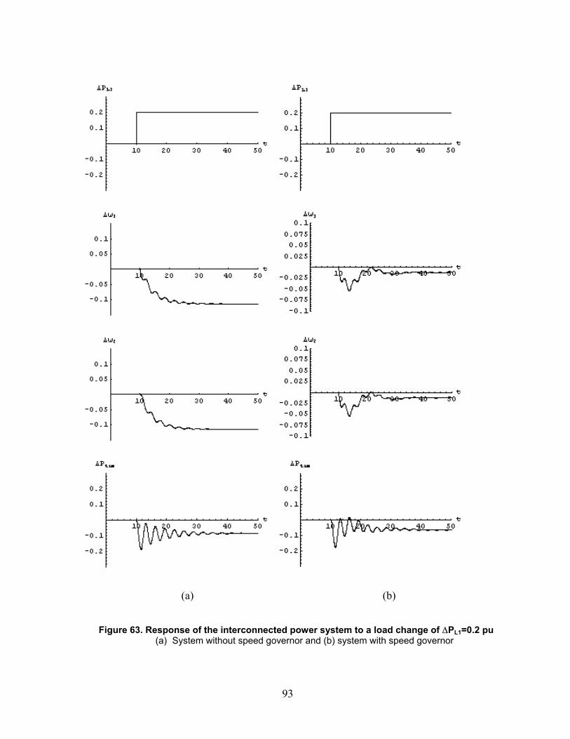
93
(a) (b)
Figure 63. Response of the interconnected power system to a load change of ∆PL1=0.2 pu (a) System without speed governor and (b) system with speed governor
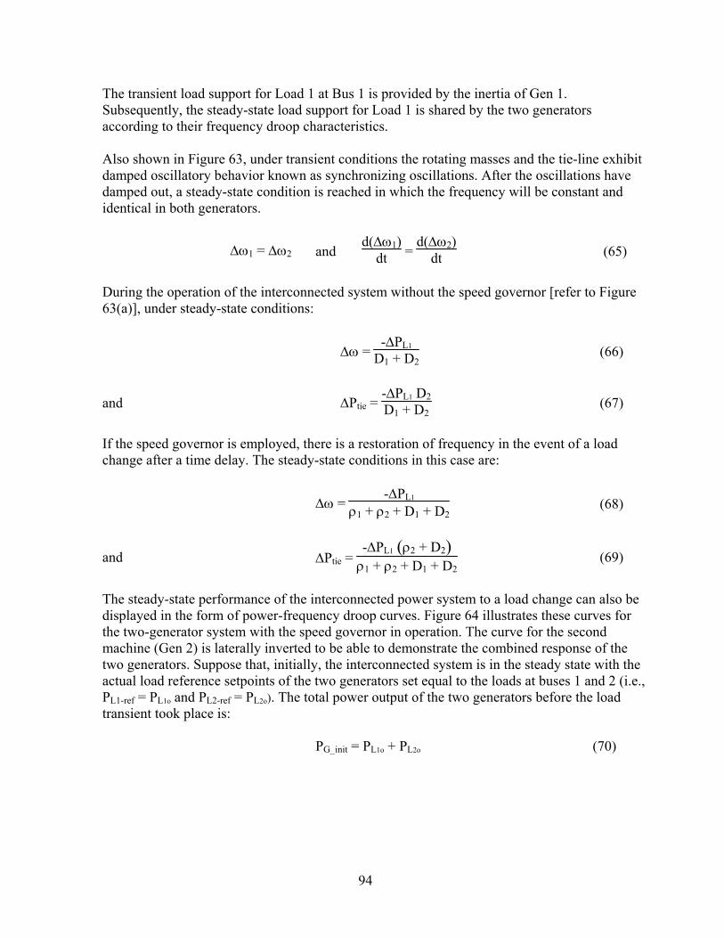
94
The transient load support for Load 1 at Bus 1 is provided by the inertia of Gen 1. Subsequently, the steady-state load support for Load 1 is shared by the two generators according to their frequency droop characteristics. Also shown in Figure 63, under transient conditions the rotating masses and the tie-line exhibit damped oscillatory behavior known as synchronizing oscillations. After the oscillations have damped out, a steady-state condition is reached in which the frequency will be constant and identical in both generators.
∆ω1 = ∆ω2 and d(∆ω1)
dt = d(∆ω2)
dt (65)
During the operation of the interconnected system without the speed governor [refer to Figure 63(a)], under steady-state conditions:
∆ω = -∆PL1
D1 + D2 (66)
and ∆Ptie = -∆PL1 D2D1 + D2
(67)
If the speed governor is employed, there is a restoration of frequency in the event of a load change after a time delay. The steady-state conditions in this case are:
∆ω = -∆PL1
ρ1 + ρ2 + D1 + D2 (68)
and ∆Ptie = -∆PL1 ( )ρ2 + D2
ρ1 + ρ2 + D1 + D2 (69)
The steady-state performance of the interconnected power system to a load change can also be displayed in the form of power-frequency droop curves. Figure 64 illustrates these curves for the two-generator system with the speed governor in operation. The curve for the second machine (Gen 2) is laterally inverted to be able to demonstrate the combined response of the two generators. Suppose that, initially, the interconnected system is in the steady state with the actual load reference setpoints of the two generators set equal to the loads at buses 1 and 2 (i.e., PL1-ref = PL1o and PL2-ref = PL2o). The total power output of the two generators before the load transient took place is: PG_init = PL1o + PL2o (70)

95
The frequency of the two machines under this condition will be identical and equal to the nominal system frequency of ωo. As shown in Figure 64, the total load is shared by the two units in accordance with their power-frequency droop. The individual slopes of the steady-state frequency-droop curves for Gen 1 and Gen 2 are respectively determined as:
∆ω1
∆PG1
∆PL1-ref = 0=
-1ρ1 (71)
and ∆ω2
∆PG2
∆PL2-ref = 0=
-1ρ2 (72)
When the load change occurs at Bus 1, the total generation in the interconnected power system is changed to: PG_final = PG1 + PG2 = PL1o + PL2o + ∆PL1 (73) With the same actual load reference setpoints as before the application of the load change (i.e., PL1-ref = PL1o and PL2-ref = PL2o), this final total load is accommodated by the interconnected system with a drop in the system frequency at steady state. It is possible to determine the final steady-state changes in individual generator outputs. The change in total generation in the interconnected power system is equal to the change in the load. ∆PG1 + ∆PG2 = ∆PL1 (74) From (71) and (72), because in steady-state ∆ω1 = ∆ω2: ∆PG1 (ρ2) = ∆PG2 (ρ1) (75) Solving (74) and (75):
∆PG1 = ∆PL1 ρ1
ρ1 + ρ2 (76)
and ∆PG2 = ∆PL1 ρ2
ρ1 + ρ2 (77)
96
Figure 64. Sharing of the load change between the two generators
in the interconnected power system
The performance of the combined system of two interconnected generators can be represented by a single power frequency-droop curve ignoring the individual dynamics, as illustrated in Figure 65. In Figure 65, the system steady-state frequency is denoted by ω, and the sum of quantities such as generation, load, and governor gains are represented by Σ. Furthermore, the power and frequency quantities before and after the load change are denoted by ’ and ”, respectively.
Figure 65. Frequency-droop curves of the interconnected power system
The frequency deviation can be eventually reduced to zero through manual coordination or automatic generation control [34, 37, 38]. Automatic generation control is beyond the scope of and is not dealt with in this report. A similar approach can be adopted to analyze interconnected power systems with more than two generators. 4.5.2 Control of Real Power Flow in a Distributed UPS System/Microgrid Figure 66 gives a simplified schematic of a UPS/DR containing the IGBT-based inverter with LCL filter and a transformer. Typically, the UPS/DR is operated to regulate the load bus voltage to a value within the tolerance limits. For that reason, the UPS/DR along with the LCL filter and transformer is approximated by a voltage source as illustrated in the figure while conducting theoretical analysis on power studies.
(ΣPL’,ω’)
ΣPG
ω
0
Slope = -(Σρ)-1
(ΣPL”,ω”)
(PL1o,ωo)(PL2o,ωo)
PL1o + PL2o + ∆PL1
PG1 PG2
ω
0
PL1o + PL2o
Slope = -(ρ1)-1
Slope = -(ρ2)-1
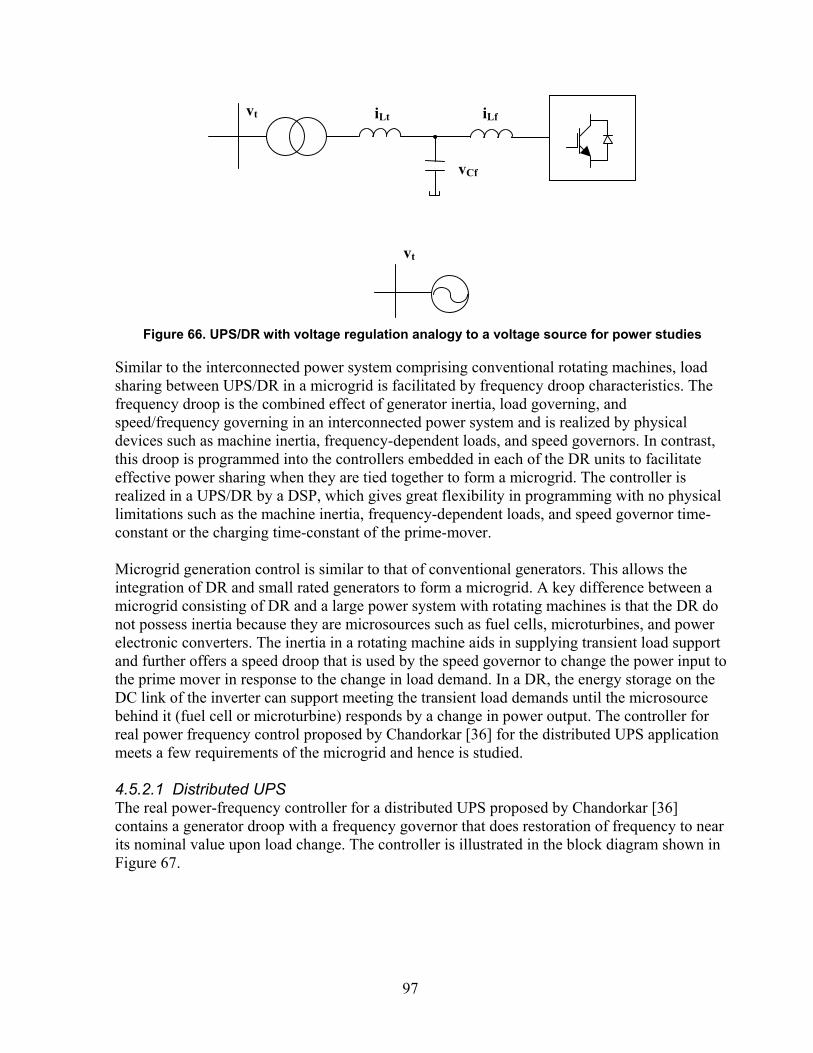
97
Figure 66. UPS/DR with voltage regulation analogy to a voltage source for power studies
Similar to the interconnected power system comprising conventional rotating machines, load sharing between UPS/DR in a microgrid is facilitated by frequency droop characteristics. The frequency droop is the combined effect of generator inertia, load governing, and speed/frequency governing in an interconnected power system and is realized by physical devices such as machine inertia, frequency-dependent loads, and speed governors. In contrast, this droop is programmed into the controllers embedded in each of the DR units to facilitate effective power sharing when they are tied together to form a microgrid. The controller is realized in a UPS/DR by a DSP, which gives great flexibility in programming with no physical limitations such as the machine inertia, frequency-dependent loads, and speed governor time-constant or the charging time-constant of the prime-mover. Microgrid generation control is similar to that of conventional generators. This allows the integration of DR and small rated generators to form a microgrid. A key difference between a microgrid consisting of DR and a large power system with rotating machines is that the DR do not possess inertia because they are microsources such as fuel cells, microturbines, and power electronic converters. The inertia in a rotating machine aids in supplying transient load support and further offers a speed droop that is used by the speed governor to change the power input to the prime mover in response to the change in load demand. In a DR, the energy storage on the DC link of the inverter can support meeting the transient load demands until the microsource behind it (fuel cell or microturbine) responds by a change in power output. The controller for real power frequency control proposed by Chandorkar [36] for the distributed UPS application meets a few requirements of the microgrid and hence is studied. 4.5.2.1 Distributed UPS The real power-frequency controller for a distributed UPS proposed by Chandorkar [36] contains a generator droop with a frequency governor that does restoration of frequency to near its nominal value upon load change. The controller is illustrated in the block diagram shown in Figure 67.
vCf
iLf iLt
vt
vt
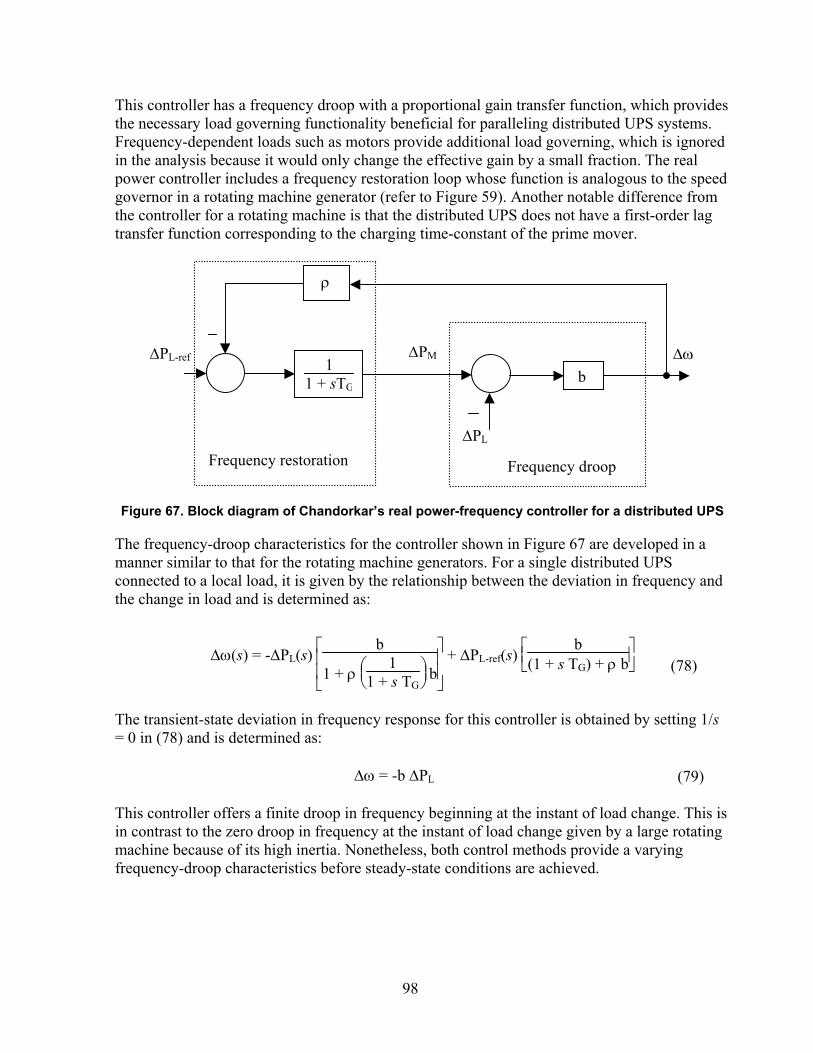
98
This controller has a frequency droop with a proportional gain transfer function, which provides the necessary load governing functionality beneficial for paralleling distributed UPS systems. Frequency-dependent loads such as motors provide additional load governing, which is ignored in the analysis because it would only change the effective gain by a small fraction. The real power controller includes a frequency restoration loop whose function is analogous to the speed governor in a rotating machine generator (refer to Figure 59). Another notable difference from the controller for a rotating machine is that the distributed UPS does not have a first-order lag transfer function corresponding to the charging time-constant of the prime mover.
Figure 67. Block diagram of Chandorkar’s real power-frequency controller for a distributed UPS
The frequency-droop characteristics for the controller shown in Figure 67 are developed in a manner similar to that for the rotating machine generators. For a single distributed UPS connected to a local load, it is given by the relationship between the deviation in frequency and the change in load and is determined as:
∆ω(s) = -∆PL(s)
b
1 + ρ
1
1 + s TG b
+ ∆PL-ref(s)
b
(1 + s TG) + ρ b (78)
The transient-state deviation in frequency response for this controller is obtained by setting 1/s = 0 in (78) and is determined as: ∆ω = -b ∆PL (79) This controller offers a finite droop in frequency beginning at the instant of load change. This is in contrast to the zero droop in frequency at the instant of load change given by a large rotating machine because of its high inertia. Nonetheless, both control methods provide a varying frequency-droop characteristics before steady-state conditions are achieved.
Frequency droop
∆PM
∆PL
∆ω
ρ
11 + sTG
Frequency restoration
b ∆PL-ref
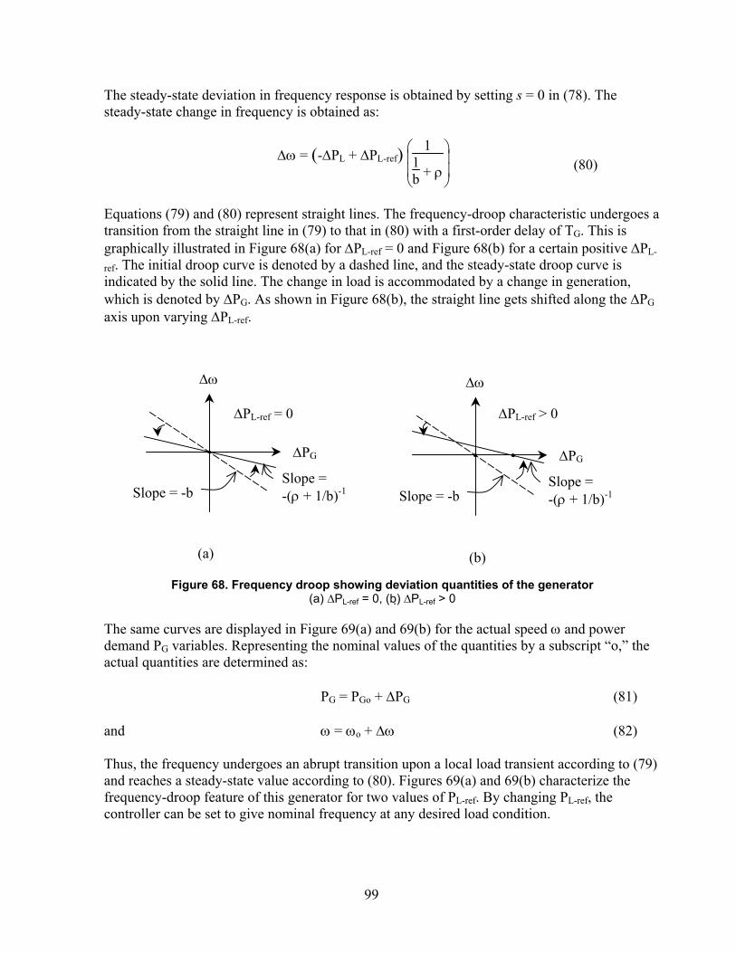
99
The steady-state deviation in frequency response is obtained by setting s = 0 in (78). The steady-state change in frequency is obtained as:
∆ω = ( )-∆PL + ∆PL-ref
1
1b + ρ (80)
Equations (79) and (80) represent straight lines. The frequency-droop characteristic undergoes a transition from the straight line in (79) to that in (80) with a first-order delay of TG. This is graphically illustrated in Figure 68(a) for ∆PL-ref = 0 and Figure 68(b) for a certain positive ∆PL-
ref. The initial droop curve is denoted by a dashed line, and the steady-state droop curve is indicated by the solid line. The change in load is accommodated by a change in generation, which is denoted by ∆PG. As shown in Figure 68(b), the straight line gets shifted along the ∆PG axis upon varying ∆PL-ref.
Figure 68. Frequency droop showing deviation quantities of the generator
(a) ∆PL-ref = 0, (b) ∆PL-ref > 0
The same curves are displayed in Figure 69(a) and 69(b) for the actual speed ω and power demand PG variables. Representing the nominal values of the quantities by a subscript “o,” the actual quantities are determined as: PG = PGo + ∆PG (81) and ω = ωo + ∆ω (82) Thus, the frequency undergoes an abrupt transition upon a local load transient according to (79) and reaches a steady-state value according to (80). Figures 69(a) and 69(b) characterize the frequency-droop feature of this generator for two values of PL-ref. By changing PL-ref, the controller can be set to give nominal frequency at any desired load condition.
∆ω
∆PG
Slope = -(ρ + 1/b)-1
∆PL-ref = 0
(b)(a)
Slope = -b
∆ω
∆PG
Slope = -(ρ + 1/b)-1
∆PL-ref > 0
Slope = -b
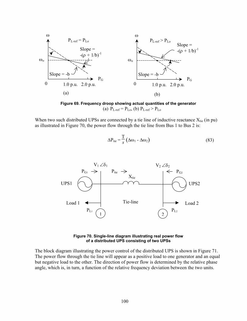
100
Figure 69. Frequency droop showing actual quantities of the generator
(a) PL-ref = PLo, (b) PL-ref > PLo
When two such distributed UPSs are connected by a tie line of inductive reactance Xtie (in pu) as illustrated in Figure 70, the power flow through the tie line from Bus 1 to Bus 2 is:
∆Ptie = Ts ( )∆ω1 - ∆ω2 (83)
Figure 70. Single-line diagram illustrating real power flow
of a distributed UPS consisting of two UPSs
The block diagram illustrating the power control of the distributed UPS is shown in Figure 71. The power flow through the tie line will appear as a positive load to one generator and an equal but negative load to the other. The direction of power flow is determined by the relative phase angle, which is, in turn, a function of the relative frequency deviation between the two units.
PG2 PG1 Ptie
PL1 PL2
Xtie
Tie-line
UPS1 UPS2
Load 1 Load 2
V1 ∠δ1 V2 ∠δ2
1 2
(b)(a)
PL-ref = PLo
1.0 p.u. 2.0 p.u.
ωo
ω
PG 0
Slope = -b
Slope = -(ρ + 1/b)-1
PL-ref > PLo
1.0 p.u. 2.0 p.u.
ωo
ω
PG 0
Slope = -b
Slope = -(ρ + 1/b)-1
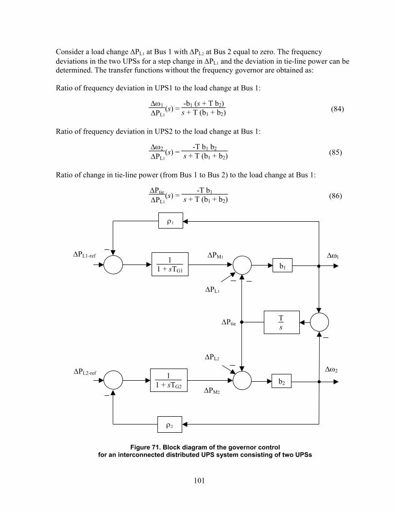
101
Consider a load change ∆PL1 at Bus 1 with ∆PL2 at Bus 2 equal to zero. The frequency deviations in the two UPSs for a step change in ∆PL1 and the deviation in tie-line power can be determined. The transfer functions without the frequency governor are obtained as: Ratio of frequency deviation in UPS1 to the load change at Bus 1:
∆ω1
∆PL1(s) =
-b1 (s + T b2)s + T (b1 + b2) (84)
Ratio of frequency deviation in UPS2 to the load change at Bus 1:
∆ω2
∆PL1(s) =
-T b1 b2 s + T (b1 + b2) (85)
Ratio of change in tie-line power (from Bus 1 to Bus 2) to the load change at Bus 1:
∆Ptie
∆PL1(s) =
-T b1 s + T (b1 + b2) (86)
Figure 71. Block diagram of the governor control
for an interconnected distributed UPS system consisting of two UPSs
∆PM1
∆PL1
∆ω111 + sTG1
∆PL1-ref
∆PM2
∆PL2
ρ2
Ts
∆ω2∆PL2-ref 11 + sTG2
∆Ptie
ρ1
b2
b1

102
The response of the interconnected power system to a step change in Load 1 of ∆PL1 = 0.2 pu (with ∆PL2 = 0) is illustrated in Figure 72. The system equations have been solved symbolically and the waveforms plotted in Mathematica software. The waveforms in Figure 72(a) demonstrate the operation without the frequency restoration. As explained earlier, a droop is observed in the frequency at the instant of load change because of the constant gain generator droop of the UPS. However, the frequency restoration loop senses this frequency deviation and changes the power output to restore the frequency close to its original value. This reduction in the frequency deviation by the use of frequency restoration is shown in Figure 72(b). The system parameters used to generate these waveforms are – b1 = 0.1 pu, b2 = 0.2 pu, T = 377/Xtie = 7.54 pu, ρ1 = 40 pu, ρ2 = 20 pu, TG1 = 10 s, TG2 = 20 s. As shown in the figure, the frequency deviation from the nominal value in steady state is reduced by the action of the governor. An important observation from Figure 72 is the response under load transients. For the case of distributed UPS operation without the frequency restoration in both the UPSs: Change in frequency deviation in UPS1 because of the load change at Bus 1 at the instant of the load transient in Load 1 [obtained by setting 1/s = 0 in (84)]: ∆ω1 = -b1 ∆PL1 (87) Change in frequency deviation in UPS2 because of the load change at Bus 1 at the instant of the load transient in Load 1 [obtained by setting 1/s = 0 in (85)]: ∆ω2 = 0 (88) Change in tie-line power (from Bus 1 to Bus 2) because of the load change at Bus 1 at the instant of the load transient in Load 1 [obtained by setting 1/s = 0 in (86)]: ∆Ptie = 0 (89) From (89), it is evident that the transient portion of the change in Load 1 at Bus 1 is not supplied by Unit 2 because of the integral gain response of the change in tie-line power for relative change in frequency in the two UPSs. Besides, the tie line does not contain stored energy to support the transient load change. This is also noticeable in Figure 72 from the instantaneous response in the deviation in frequency ∆ω1 compared with the deviations in tie-line power ∆Ptie or in frequency ∆ω2. The unequal change in frequency deviations of the two UPSs at the instant of load transient causes a rapid change in the relative phase angle between buses 1 and 2. As a result, the duration for which the total load transient at Bus 1 is supported by only UPS1 is the bare minimum. The load sharing by the two UPSs begins at an earlier stage in this control compared with that of a conventional rotating machine. This is beneficial if employed for a microgrid consisting of DR because the microsources (such as fuel cells or microturbines) do not have to support transient power demands. The energy storage in the DC link of UPS1 provides the transient load support for Load 1 at the instant of load change. Another observation from Figure 72 is that there is no oscillatory behavior (otherwise known as synchronizing oscillations) in the microgrid system consisting of two UPSs.
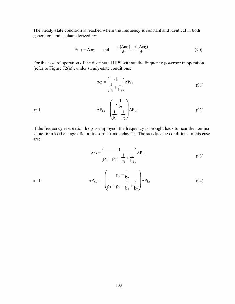
103
The steady-state condition is reached where the frequency is constant and identical in both generators and is characterized by:
∆ω1 = ∆ω2 and d(∆ω1)
dt = d(∆ω2)
dt (90)
For the case of operation of the distributed UPS without the frequency governor in operation [refer to Figure 72(a)], under steady-state conditions:
∆ω =
-1
1b1
+ 1b2
∆PL1 (91)
and ∆Ptie =
-
1b2
1b1
+ 1b2
∆PL1 (92)
If the frequency restoration loop is employed, the frequency is brought back to near the nominal value for a load change after a first-order time delay TG. The steady-state conditions in this case are:
∆ω =
-1
ρ1 + ρ2 + 1b1
+ 1b2
∆PL1 (93)
and ∆Ptie = -
ρ2 +
1b2
ρ1 + ρ2 + 1b1
+ 1b2
∆PL1 (94)
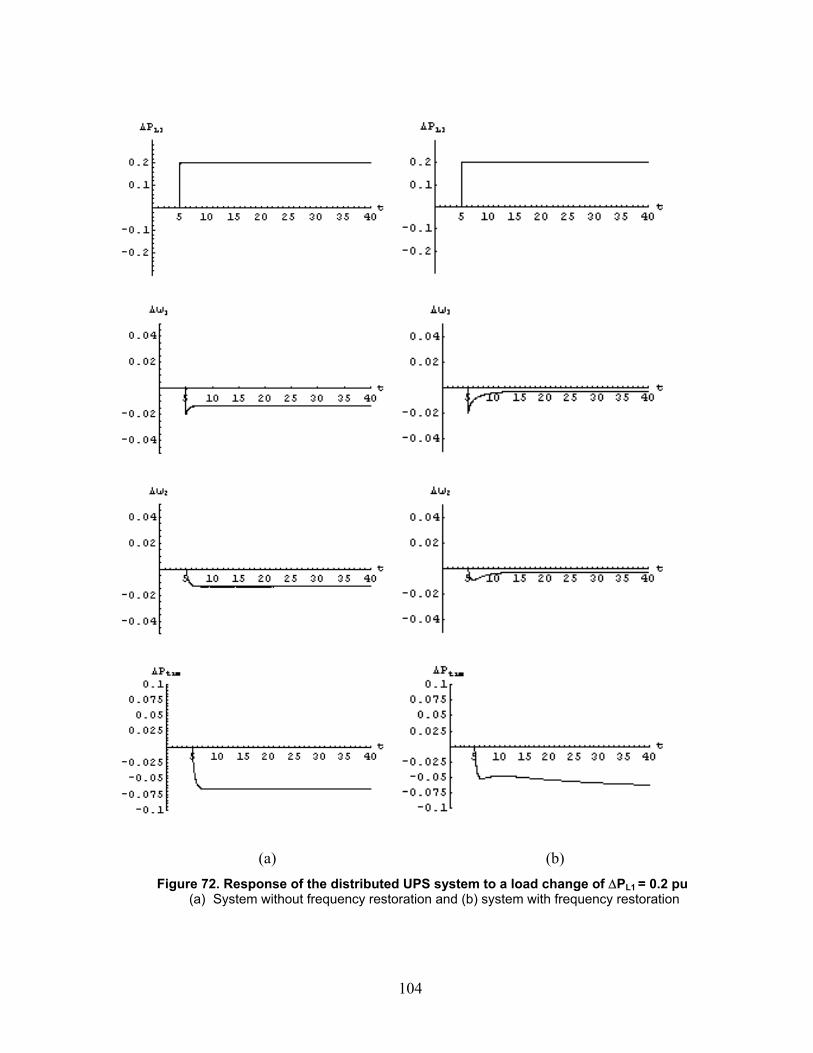
104
(a) (b)
Figure 72. Response of the distributed UPS system to a load change of ∆PL1 = 0.2 pu (a) System without frequency restoration and (b) system with frequency restoration
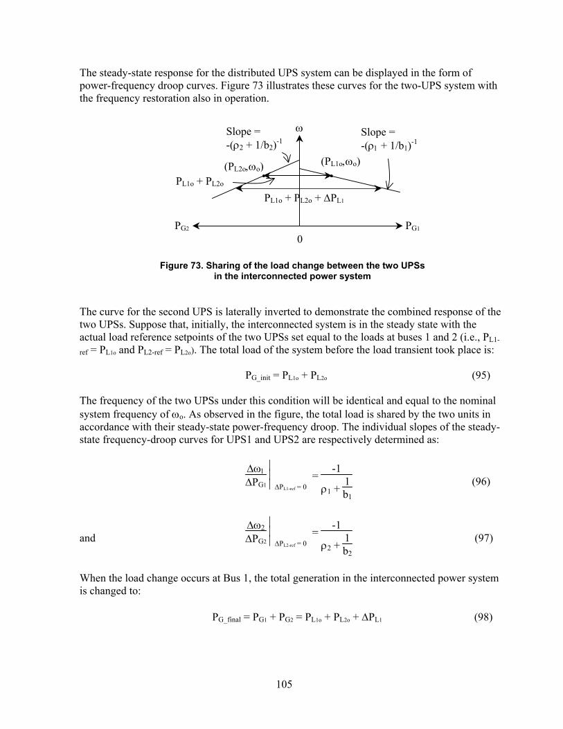
105
The steady-state response for the distributed UPS system can be displayed in the form of power-frequency droop curves. Figure 73 illustrates these curves for the two-UPS system with the frequency restoration also in operation.
Figure 73. Sharing of the load change between the two UPSs
in the interconnected power system
The curve for the second UPS is laterally inverted to demonstrate the combined response of the two UPSs. Suppose that, initially, the interconnected system is in the steady state with the actual load reference setpoints of the two UPSs set equal to the loads at buses 1 and 2 (i.e., PL1-
ref = PL1o and PL2-ref = PL2o). The total load of the system before the load transient took place is: PG_init = PL1o + PL2o (95) The frequency of the two UPSs under this condition will be identical and equal to the nominal system frequency of ωo. As observed in the figure, the total load is shared by the two units in accordance with their steady-state power-frequency droop. The individual slopes of the steady-state frequency-droop curves for UPS1 and UPS2 are respectively determined as:
∆ω1
∆PG1
∆PL1-ref = 0=
-1
ρ1 + 1b1
(96)
and ∆ω2
∆PG2
∆PL2-ref = 0=
-1
ρ2 + 1b2
(97)
When the load change occurs at Bus 1, the total generation in the interconnected power system is changed to: PG_final = PG1 + PG2 = PL1o + PL2o + ∆PL1 (98)
(PL1o,ωo)(PL2o,ωo)
PL1o + PL2o + ∆PL1
PG1 PG2
ω
0
PL1o + PL2o
Slope = -(ρ1 + 1/b1)-1
Slope = -(ρ2 + 1/b2)-1
106
With the same actual load reference setpoints as before the application of the load change (i.e., PL1-ref = PL1o and PL2-ref = PL2o), this final total load is accommodated by the interconnected system with a drop in the system frequency at steady state. It is possible to determine the final steady-state changes in individual UPS outputs. The change in total generation in the interconnected distributed UPS system is equal to the change in the load. ∆PG1 + ∆PG2 = ∆PL1 (99) From (97) and (96), because in steady-state ∆ω1 = ∆ω2: ∆PG1 (ρ2 + 1/b2) = ∆PG2 (ρ1 + 1/b1) (100) Solving (99) and (100):
∆PG1 = ∆PL1 ρ1 + 1/b1
ρ1 + ρ2 + 1/b1 + 1/b2 (101)
and ∆PG2 = ∆PL1 ρ2 + 1/b2
ρ1 + ρ2 + 1/b1 + 1/b2 (102)
The steady-state frequency deviation is given by (93). The performance of the combined system of two UPSs can be represented by a single power-frequency droop curve, ignoring the individual dynamics, as illustrated in Figure 74. In Figure 74, the system steady-state frequency is denoted by ω, and the sum of the quantities such as generation, load, and governor gains are represented by Σ. Furthermore, the power and frequency quantities before and after the load change are denoted by ’ and ”, respectively.
Figure 74. Frequency-droop curves of the interconnected power system
A similar approach can be adopted to analyze distributed UPS systems with more than two UPSs.
(ΣPL’,ω’)
ΣPG
ω
0
Slope = -(Σρ + Σ(1/b))-1
(ΣPL”,ω”)

107
4.5.2.2 Microgrid Consisting of Distributed Resources As demonstrated in the previous subsection, the controller proposed by Chandorkar [36] for distributed UPS applications allows real power sharing among several interconnected UPS units. For a single distributed UPS unit, the deviation in frequency ∆ω to the deviation in load demand ∆PL alone is given by:
∆ω(s)
∆PL-ref(s) = 0= -∆PL(s)
b
1 + ρ
1
1 + s TG b (103)
However, the basic control input for generation control of a generating unit is the load reference setpoint ∆PL-ref [34]. The feature of dispatchability in a microgrid relies heavily on the system response to a change in load reference setpoint ∆PL-ref. Because the objective of this project is to use the microgrid to provide reliable power to power quality-sensitive loads, the response to a change in ∆PL-ref must be nearly as quick as that for a change in ∆PL. The deviation in frequency ∆ω of the distributed UPS using Chandorkar’s controller [36] to a change in the load reference setpoint ∆PL-ref alone, for a single distributed UPS unit, is given by:
∆ω(s)
∆PL(s) = 0= ∆PL-ref(s)
b
(1 + ρ b) + s TG (104)
Figure 75 illustrates the two responses of (103) and (104) with the following parameters: b = 0.1 pu, ρ = 10 pu, and TG = 10 s. As shown in the figure, although the ∆ω response to a change in load demand ∆PL has an initial overshoot before settling to the steady-state value, the response to a change in the load reference setpoint ∆PL-ref is smooth and settles to the final value at the same time. This is due to the effect of the first-order lag transfer function with time-constant TG on the load reference setpoint input ∆PL-ref.
108
(a) (b)
Figure 75. Single distributed UPS unit (a) Response to a step change in load ∆PL = 0.2 pu
(b) Response to a step change in load reference setpoint ∆PL-ref = 0.2 pu
Therefore, Chandorkar’s controller is used for real power control in a DR. The block diagram of the real power-frequency controller for a DR is identical to that for a distributed UPS and is illustrated in Figure 76.
Figure 76. Block diagram of Chandorkar’s real power-frequency controller for a DR
Frequency droop
∆PM
∆PL
∆ω
ρ
11 + sTG
Frequency restoration
b ∆PL-ref
109
When two DR are connected by a tie line of inductive reactance Xtie (in pu) as illustrated in Figure 77, the real power flow through the tie line from Bus 1 to Bus 2 is:
∆Ptie = Ts ( )∆ω1 - ∆ω2 (105)
Figure 77. Single-line diagram illustrating real power flow of a microgrid consisting of two DR
The block diagram illustrating real power control of the DR is shown in Figure 78. The power flow through the tie line will appear as a positive load to one generator and an equal but negative load to the other. The direction of power flow is determined by the relative phase angle, which is, in turn, a function of the relative frequency deviation between the two units.
PG2 PG1 Ptie
PL1 PL2
Xtie
Tie-line
DR1 DR2
Load 1 Load 2
V1 ∠δ1 V2 ∠δ2
1 2
110
Figure 78. Block diagram of the frequency droop and governor control
for a microgrid consisting of two DR
Consider a load reference setpoint change ∆PL1-ref at Bus 1 with ∆PL2-ref being equal to zero. The frequency deviations in the two DR as well as the deviation in tie-line power for a step change in ∆PL1-ref can be determined. The response to a change in ∆PL1 for the microgrid, keeping the deviation in load ∆PL2 fixed at zero, is shown in Figure 79(a). Likewise, the response to a change in ∆PL1-ref, keeping the deviations in load ∆PL1 and ∆PL2 fixed at zero, is shown in Figure 79(b). It is assumed that the frequency restoration loop is active. The system equations have been solved symbolically and the waveforms plotted in Mathematica software. As shown in the figure, the load reference setpoint ∆PL1-ref has a smooth response on the power generation of the two DR units compared with the response for ∆PL1. Moreover, a change in the load reference setpoint ∆PL1-ref in DR1 in the microgrid leads to a change in the proportion of total load shared by DR1 and DR2.
∆PM1
∆PL1
∆ω111 + sTG1
∆PL1-ref
∆PM2
∆PL2
ρ2
Ts
∆ω2∆PL2-ref 11 + sTG2
∆Ptie
ρ1
b2
b1
111
(a) (b)
Figure 79. Response of the microgrid to (a) load change of ∆PL1 = 0.2 pu and (b) load reference setpoint change of ∆PL1-ref = 0.2 pu
112
The system parameters used to generate these waveforms are: b1 = 0.1 pu, b2 = 0.2 pu, T = 377/Xtie = 7.54 pu, ρ1 = 40 pu, ρ2 = 20 pu, TG1 = 10 s, and TG2 = 20 s. The steady-state response showing the effect of change in ∆PL1-ref can be displayed in the form of power-frequency droop curves. Figure 80 illustrates these curves for the system containing two units. The curve for the second unit is laterally inverted to demonstrate the combined response of the two units. Suppose that, initially, the interconnected system is in the steady state with the actual load reference setpoints of the two units set equal to the loads at buses 1 and 2 (i.e., PL1-ref = PL1o and PL2-ref = PL2o). The total load of the system before the load transient took place is: PG_init = PL1o + PL2o (106) The slopes of the two frequency droop curves are:
Slope1 =
-1
ρ1 + 1b1
(107)
and Slope2 =
-1
ρ2 + 1b2
(108)
When the load reference setpoint is changed to PL1-ref = PL1o + ∆PL1-ref in the frequency governor of Unit 1, the total load in the interconnected system is redistributed as illustrated in Figure 80. The frequency droop curve of Unit 1 before the change in ∆PL1-ref is shown by a dashed line; that after the change in ∆PL1-ref is shown by a solid line. PG_final = PG1 + PG2 = PL1o + PL2o (109) With a change in the same actual load reference setpoint and with no load change (i.e., ∆PL1 = 0 and ∆PL2 = 0), this total load is accommodated by the interconnected system with a change in the system frequency at steady state.
Figure 80. Sharing of load change between the two units in the interconnected system
(PL1o,ωo)
(PL2o,ωo)
PG1PG2
ω
0
PL1o + PL2o
Slope = -(ρ1 + 1/b1)-1
Slope = -(ρ2 + 1/b2)-1
∆PL1-ref causes the shift
∆PL1-ref
113
It is possible to determine the final steady-state changes in individual unit outputs. The change in total generation in the interconnected distributed UPS system is equal to the change in the load. ∆PG1 + ∆PG2 = ∆PL = 0 (110) The steady-state deviations in frequencies of units 1 and 2 are determined as:
∆ω1 = -∆PG1
1
ρ1 + 1b1
+ ∆PL1-ref 1
ρ1 + 1b1
(111)
∆ω2 = -∆PG2
1
ρ2 + 1b2
(112)
Because in steady state ∆ω1 = ∆ω2, equating (111) and (112): (∆PG1 - ∆PL1-ref) (ρ2 + 1/b2) = ∆PG2 (ρ1 + 1/b1) (113) Solving (110) and (113):
∆PG1 = ∆PL1-ref ρ2 + 1/b2
ρ1 + ρ2 + 1/b1 + 1/b2 (114)
and ∆PG2 = -∆PL1-ref ρ2 + 1/b2
ρ1 + ρ2 + 1/b1 + 1/b2 (115)
Thus, a change in the load reference setpoint of Unit 1 causes a change in generation of both Unit 1 and Unit 2. The steady-state deviation in frequency ∆ω is determined by substituting (115) in (112) as:
∆ω = ∆PL1-ref 1
ρ1 + ρ2 + 1/b1 + 1/b2 (116)
The performance of the combined system of two UPSs can be represented by a single power-frequency droop curve, ignoring the individual dynamics, as illustrated in Figure 81. In Figure 81, the system steady-state frequency is denoted by ω, and the sum of the quantities such as generation, load, and governor gains are represented by Σ. Furthermore, the nominal values of power and frequency quantities are denoted by a subscript o.

114
Figure 81. Frequency-droop curves of the interconnected power system
A similar approach can be adopted to analyze interconnected systems of more than two units. 4.6 Control of Reactive Power in a Microgrid The DR in a microgrid employ semiconductor devices in the power electronic converters. Because the current capacity of these semiconductor devices is limited, it is necessary to control the apparent power drawn from a DR in a microgrid. This can be achieved by having a controller for regulating reactive power drawn from the DR along with the real power regulator described earlier. The real power control is performed by means of the frequency droop characteristics. The reactive power regulation can be performed by exploiting the dependency of the reactive power supplied by the DR on the voltage magnitude at the load bus. Figure 82 shows a simplified schematic of the proposed reactive power controller. The DR modeling for reactive power-voltage control is similar to the real power-frequency control in a conventional rotating machine. A first-order lag is employed for the deviation in reactive power as: ∆QM – ∆QL-total = (L s + R) ∆V (117) The reactive loads in a power system can be categorized broadly as those that are voltage-independent and those that are sensitive to voltage. In a power system, the voltage-dependent loads are passive loads such as inductive or capacitive loads as well as motor loads [39]. Such loads contribute to load governing in the DR. The relationship between change in load and change in voltage is: ∆QL(freq) = R’ ∆V (118) Representing the voltage-independent reactive loads by ∆QL, the net change in load reactive power is given by: ∆QL-total = ∆QL + R’ ∆V (119)
ΣPG
ω
0
Slope = -(Σρ + Σ(1/b))-1
(ΣPLo,ωο)Σ∆PL-ref
115
Substituting (119) in (117): ∆QM = (L s + R + R') ∆V (120) By designing R >> R’, it can be assumed that R + R’ ≈ R. Therefore: ∆QM ≈ (L s + R) ∆V (121) Similar to the frequency governor of the real power-frequency control described earlier, a voltage regulator consisting of a voltage restoring loop is included in the reactive power controller. This loop is modeled by a gain ρ for the voltage error and a time-constant TG. It is noted that the voltage droop as well as the voltage restoration loop are programmed in a DSP controller, and any load governing that may take place because of voltage-dependent reactive loads is a natural occurrence. In Figure 82, the input labeled ∆QL-ref is the load reference setpoint that is the control input to shift the generator’s voltage regulator characteristic to give the reference voltage at any desired reactive power output.
Figure 82. Block diagram of the proposed reactive power controller for a DR
To generate the voltage droop characteristics of the DR with the proposed controller, the relation between the deviation in voltage and the change in reactive load is examined. This relationship is:
∆V(s) =
-∆QL(s)L s + R
1 + ρ
1
1 + s TG
1
L s + R
+
∆QL-ref(s)L s + R
(1 + s TG) + ρ
1
L s + R
(122)
Voltage droop
∆QM
∆QL
∆V
ρ
11 + sTG
Voltage regulator
∆QL-ref
1
Ls + R
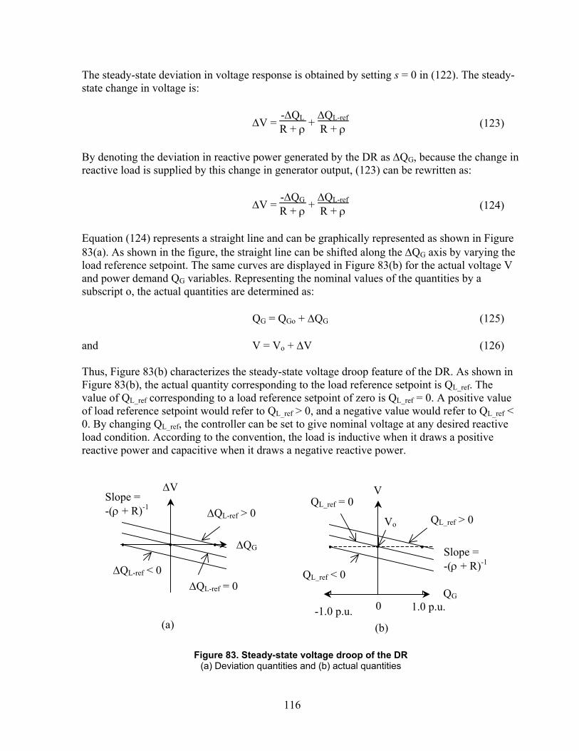
116
The steady-state deviation in voltage response is obtained by setting s = 0 in (122). The steady-state change in voltage is:
∆V = -∆QL
R + ρ + ∆QL-ref
R + ρ (123)
By denoting the deviation in reactive power generated by the DR as ∆QG, because the change in reactive load is supplied by this change in generator output, (123) can be rewritten as:
∆V = -∆QG
R + ρ + ∆QL-ref
R + ρ (124)
Equation (124) represents a straight line and can be graphically represented as shown in Figure 83(a). As shown in the figure, the straight line can be shifted along the ∆QG axis by varying the load reference setpoint. The same curves are displayed in Figure 83(b) for the actual voltage V and power demand QG variables. Representing the nominal values of the quantities by a subscript o, the actual quantities are determined as: QG = QGo + ∆QG (125) and V = Vo + ∆V (126) Thus, Figure 83(b) characterizes the steady-state voltage droop feature of the DR. As shown in Figure 83(b), the actual quantity corresponding to the load reference setpoint is QL_ref. The value of QL_ref corresponding to a load reference setpoint of zero is QL_ref = 0. A positive value of load reference setpoint would refer to QL_ref > 0, and a negative value would refer to QL_ref < 0. By changing QL_ref, the controller can be set to give nominal voltage at any desired reactive load condition. According to the convention, the load is inductive when it draws a positive reactive power and capacitive when it draws a negative reactive power.
Figure 83. Steady-state voltage droop of the DR
(a) Deviation quantities and (b) actual quantities
QL_ref < 0
QL_ref = 0 QL_ref > 0
1.0 p.u.
Vo
V
QG 0
Slope = -(ρ + R)-1
∆V
∆QG
Slope = -(ρ + R)-1
(b)(a)
∆QL-ref > 0
∆QL-ref = 0∆QL-ref < 0
-1.0 p.u.
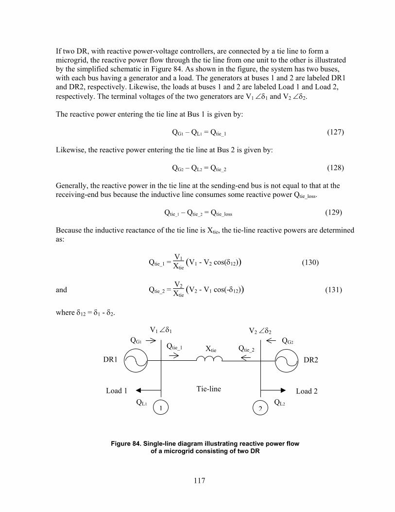
117
If two DR, with reactive power-voltage controllers, are connected by a tie line to form a microgrid, the reactive power flow through the tie line from one unit to the other is illustrated by the simplified schematic in Figure 84. As shown in the figure, the system has two buses, with each bus having a generator and a load. The generators at buses 1 and 2 are labeled DR1 and DR2, respectively. Likewise, the loads at buses 1 and 2 are labeled Load 1 and Load 2, respectively. The terminal voltages of the two generators are V1 ∠δ1 and V2 ∠δ2. The reactive power entering the tie line at Bus 1 is given by: QG1 – QL1 = Qtie_1 (127) Likewise, the reactive power entering the tie line at Bus 2 is given by: QG2 – QL2 = Qtie_2 (128) Generally, the reactive power in the tie line at the sending-end bus is not equal to that at the receiving-end bus because the inductive line consumes some reactive power Qtie_loss. Qtie_1 – Qtie_2 = Qtie_loss (129) Because the inductive reactance of the tie line is Xtie, the tie-line reactive powers are determined as:
Qtie_1 = V1Xtie
( )V1 - V2 cos(δ12) (130)
and Qtie_2 = V2Xtie
( )V2 - V1 cos(-δ12) (131)
where δ12 = δ1 - δ2.
Figure 84. Single-line diagram illustrating reactive power flow
of a microgrid consisting of two DR
QG2 QG1 Qtie_1
QL1 QL2
Xtie
Tie-line
DR1 DR2
Load 1 Load 2
V1 ∠δ1 V2 ∠δ2
1 2
Qtie_2

118
Assuming that δ12 is very small: cos(δ12) ≈ 1 (132) Substituting (132) in (130) and (131):
Qtie_1 = V1Xtie
( )V1 - V2 (133)
and Qtie_2 = V2Xtie
( )V2 - V1 (134)
Denoting the steady-state quantities by a subscript o, the steady-state power flow through the tie line is given by:
Qtie_1 o = V1oXtie
( )V1o - V2o (135)
and Qtie_2 o = V2oXtie
( )V2o - V1o (136)
Consider small deviations in the quantities from their nominal/steady-state values. Designating the deviations by a ∆ and recognizing the fact that the deviations in the voltages have a dominant effect on the reactive power flow:
Qtie_1 o + ∆Qtie_1 ≈ V1oXtie
( )(V1o + ∆V1) - (V2o + ∆V2) (137)
and Qtie_2 o + ∆Qtie_2 ≈ V2oXtie
( )(V2o + ∆V2) - (V1o + ∆V1) (138)
From (135) and (137):
∆Qtie_1 = V1oXtie
( )∆V1 - ∆V2 (139)
Likewise, from (136) and (138):
∆Qtie_2 = V2oXtie
( )∆V2 - ∆V1 (140)
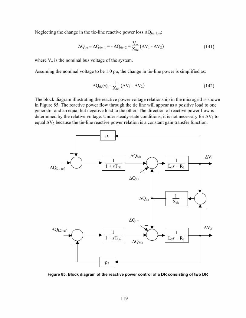
119
Neglecting the change in the tie-line reactive power loss ∆Qtie_loss:
∆Qtie = ∆Qtie_1 = - ∆Qtie_2 = VoXtie
( )∆V1 - ∆V2 (141)
where Vo is the nominal bus voltage of the system. Assuming the nominal voltage to be 1.0 pu, the change in tie-line power is simplified as:
∆Qtie(s) = 1
Xtie ( )∆V1 - ∆V2 (142)
The block diagram illustrating the reactive power voltage relationship in the microgrid is shown in Figure 85. The reactive power flow through the tie line will appear as a positive load to one generator and an equal but negative load to the other. The direction of reactive power flow is determined by the relative voltage. Under steady-state conditions, it is not necessary for ∆V1 to equal ∆V2 because the tie-line reactive power relation is a constant gain transfer function.
Figure 85. Block diagram of the reactive power control of a DR consisting of two DR
∆QM1
∆QL1
∆V1
∆QL1-ref
∆QM2
∆QL2
ρ2
1
Xtie
∆V2∆QL2-ref 11 + sTG2
∆Qtie
ρ1
11 + sTG1
1L2s + R2
1L1s + R1
120
Consider a load change ∆QL1 in Bus 1 with ∆QL2 in Bus 2 equal to zero. The relationship between the system variables against change in load ∆QL1 can be determined when the voltage restoration loop is present as well as when it is not present. The transfer functions without the voltage restoration loop are obtained as: Ratio of frequency deviation in DR1 to the load change at Bus 1:
∆V1
∆QL1(s) =
-[Xtie (L2 s + R2) + 1](L1 s + R1) [Xtie (L2 s + R2) + 1] + (L2 s + R2) (143)
Ratio of frequency deviation in DR2 to the load change at Bus 1:
∆V2
∆QL1(s) =
-1(L1 s + R1) [Xtie (L2 s + R2) + 1] + (L2 s + R2) (144)
Ratio of change in tie-line reactive power (from Bus 1 to Bus 2) to the load change at Bus 1:
∆Qtie
∆QL1(s) =
-(L2 s + R2)(L1 s + R1) [Xtie (L2 s + R2) + 1] + (L2 s + R2) (145)
The response of the microgrid to a step change in the reactive load at Bus 1 of ∆QL1 = 0.2 pu (with ∆QL2 = 0) is illustrated in Figure 87. The equations have been solved symbolically and the waveforms plotted in Mathematica software. The waveforms in Figure 87(a) demonstrate the operation without the voltage restoration loop. It is observed that the generator droop together with the load governing, which can be approximated as a first-order lag transfer function, causes an exponential response in the deviation in voltage response to a step change in the deviation in the load reactive power QL. A notable outcome of reactive power control is that the steady-state deviation in voltage at both the DR buses is not matching, departing from the matching steady-state deviation in frequency in real power frequency control. This is because the constant gain modeling of the transmission line for reactive power [refer to (142)]. However, when a voltage regulator is added in the controller, this voltage deviation is restored close to the zero value after a time delay. The decrease in the voltage deviation by the use of the voltage regulator is observed in the waveforms shown in Figure 87(b). The system parameters used to generate these waveforms are: L1 = 3.5 pu, R1 = 3.0, L2 = 4.0 pu, R2 = 2.75, Xtie = 50 pu, ρ1 = 10 pu, ρ2 = 5 pu, TG1 = 10 s, and TG2 = 20 s.
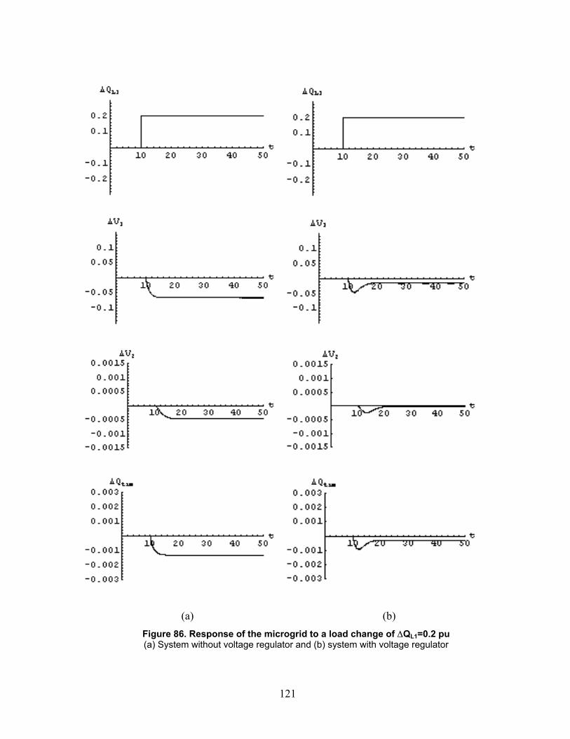
121
(a) (b)
Figure 86. Response of the microgrid to a load change of ∆QL1=0.2 pu (a) System without voltage regulator and (b) system with voltage regulator

122
The steady-state responses to a step change in reactive load can be estimated analytically as well. During the operation of the interconnected system without the voltage regulator [refer to Figure 87(a)]:
∆V1 = -∆QL1 (Xtie R2 + 1)
R1 (Xtie R2 + 1) + R2 (146)
∆V2 = -∆QL1
R1 (Xtie R2 + 1) + R2 (147)
and ∆Qtie = -∆QL1 R2
R1 (Xtie R2 + 1) + R2 (148)
If the voltage regulator is employed, there is a restoration of voltage near the nominal value after a time delay in the event of a load change. The steady-state conditions in this case are:
∆V1 = -∆QL1
( )Xtie ( )R2 + ρ2 + 1
( )R1 + ρ1 ( )Xtie ( )R2 + ρ2 + 1 + ( )R2 + ρ2 (149)
∆V2 = -∆QL1
1
( )R1 + ρ1 ( )Xtie ( )R2 + ρ2 + 1 + ( )R2 + ρ2 (150)
and ∆Qtie = -∆QL1
( )R2 + ρ2
( )R1 + ρ1 ( )Xtie ( )R2 + ρ2 + 1 + ( )R2 + ρ2 (151)
The reactive power-voltage expressions in (146) through (151) are influenced by the tie-line reactance unlike the corresponding real power-frequency expressions derived earlier, which are independent of the tie-line parameters. Moreover, there is no common steady-state parameter; this makes it difficult to find a commonality between the two DR, and so there is no advantage in giving a graphical display of the voltage droop curves for representing reactive power sharing between the DR connected to form a microgrid. 4.7 Grid-Interfaced Mode of Operation of the Microgrid The grid supply generally has enormous generation capacity compared with the microgrid. For this reason, the grid supply can be modeled as an infinite bus with the characteristics of stiff voltage and frequency, and, accordingly, the real power-frequency and reactive power-voltage droop curves are horizontal for a supply of stiff voltage and frequency, as indicated in Figure 87.
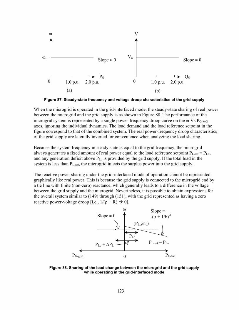
123
Figure 87. Steady-state frequency and voltage droop characteristics of the grid supply
When the microgrid is operated in the grid-interfaced mode, the steady-state sharing of real power between the microgrid and the grid supply is as shown in Figure 88. The performance of the microgrid system is represented by a single power-frequency droop curve on the ω Vs PG-MG axes, ignoring the individual dynamics. The load demand and the load reference setpoint in the figure correspond to that of the combined system. The real power-frequency droop characteristics of the grid supply are laterally inverted for convenience when analyzing the load sharing. Because the system frequency in steady state is equal to the grid frequency, the microgrid always generates a fixed amount of real power equal to the load reference setpoint PL-ref = PLo, and any generation deficit above PLo is provided by the grid supply. If the total load in the system is less than PL-ref, the microgrid injects the surplus power into the grid supply. The reactive power sharing under the grid-interfaced mode of operation cannot be represented graphically like real power. This is because the grid supply is connected to the microgrid end by a tie line with finite (non-zero) reactance, which generally leads to a difference in the voltage between the grid supply and the microgrid. Nevertheless, it is possible to obtain expressions for the overall system similar to (149) through (151), with the grid represented as having a zero reactive power-voltage droop [i.e., 1/(ρ + R) 0].
Figure 88. Sharing of the load change between the microgrid and the grid supply
while operating in the grid-interfaced mode
(PLo,ωo)
PLo + ∆PL
PG-MG PG-grid
ω
0
PLo
Slope = -(ρ + 1/b)-1 Slope ≈ 0
PL-ref = PLo
1.0 p.u. 2.0 p.u.
Vo
V
QG 0
Slope ≈ 0
(b)(a)
1.0 p.u. 2.0 p.u.
ωo
PG 0
Slope ≈ 0
ω

124
This chapter presented the design of the controller to operate the DR under imbalanced conditions. The internal voltage and current controllers are designed to regulate the sensitive load bus voltage even under negative sequence imbalances. Zero sequence imbalances do not exist on the DR side of the delta-wye transformer because of the three-wire nature of the connection. The voltage regulator makes use of a novel complex control technique to achieve a zero steady-state error. The external real and reactive power regulators vary the frequency and voltage of the DR and thereby allow paralleling of DR in the microgrid. The detailed design and performance analysis was conducted for a decentralized controller for the individual DR in the microgrid. With the help of the designed controllers, the DR are capable of providing reliable power with power quality conditioning capabilities to sensitive loads.

125
5 Distributed Resource Controller Experimental Implementation
The construction of the laboratory-scale microgrid with two inverters, filters, transformers, interconnection wiring, circuit breakers and protection equipment, synchronizing circuitry, and static switch was completed using commercial and custom-designed hardware. The power circuit elements were individually tested to verify proper operation. Detailed operating characteristics and representative test results were provided in the report of Phase I of the project. The power circuit hardware was supplemented to incorporate the control approaches developed to verify appropriate operation. Some issues with digital implementation of the controller presented in the preceding chapter were discovered during the experimental testing. Some of the experimental results demonstrating the practical implementation issues of the digital controller are presented in this chapter. The DR controller is programmed in a Motorola 56F805 DSP, which is a 16-bit, fixed-point DSP with microcontroller functionality [40]. The DSP has dedicated peripherals including a PWM module, an analog-to-digital converter, timers, and on-board Flash and RAM that are well-suited for power-electronic/motor-drive applications. The implementation issues presented in this section are divided into two sections: (1) the internal voltage and current regulators and (2) the external power regulators. 5.1 Internal Voltage and Current Regulator Implementation The internal voltage and current regulators are implemented in the stationary reference frame by the complex controller described in Chapter 4. The controller operates on three-phase AC sinusoidal quantities. However, practical measurements of the AC voltages and currents contain a small quantity of DC offset that gets carried over to the PWM voltage reference. Figure 89 illustrates the DC offset in measurements of voltage and current. The DC offset in the measured signals degrades the performance of the stationary reference frame controller. It also leads to the transformer saturation. These problems have been solved by employing a high-pass filter in the digital controller or signal conditioning hardware.
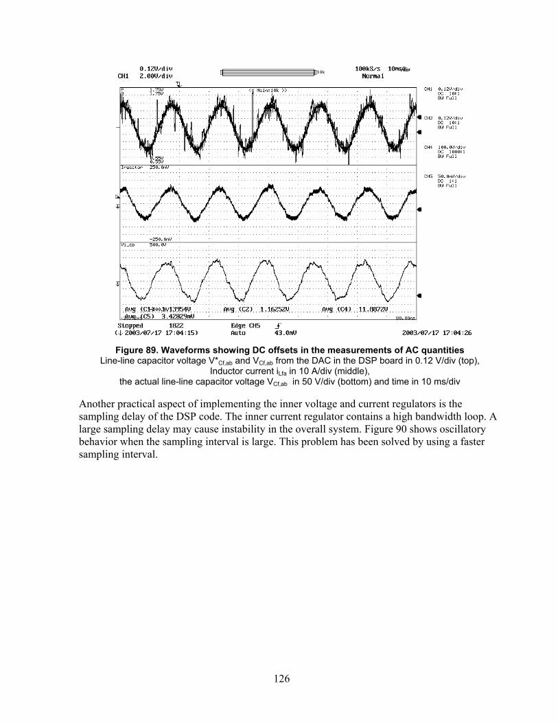
126
Figure 89. Waveforms showing DC offsets in the measurements of AC quantities
Line-line capacitor voltage V*Cf,ab and VCf,ab from the DAC in the DSP board in 0.12 V/div (top), Inductor current iLfa in 10 A/div (middle),
the actual line-line capacitor voltage VCf,ab in 50 V/div (bottom) and time in 10 ms/div
Another practical aspect of implementing the inner voltage and current regulators is the sampling delay of the DSP code. The inner current regulator contains a high bandwidth loop. A large sampling delay may cause instability in the overall system. Figure 90 shows oscillatory behavior when the sampling interval is large. This problem has been solved by using a faster sampling interval.
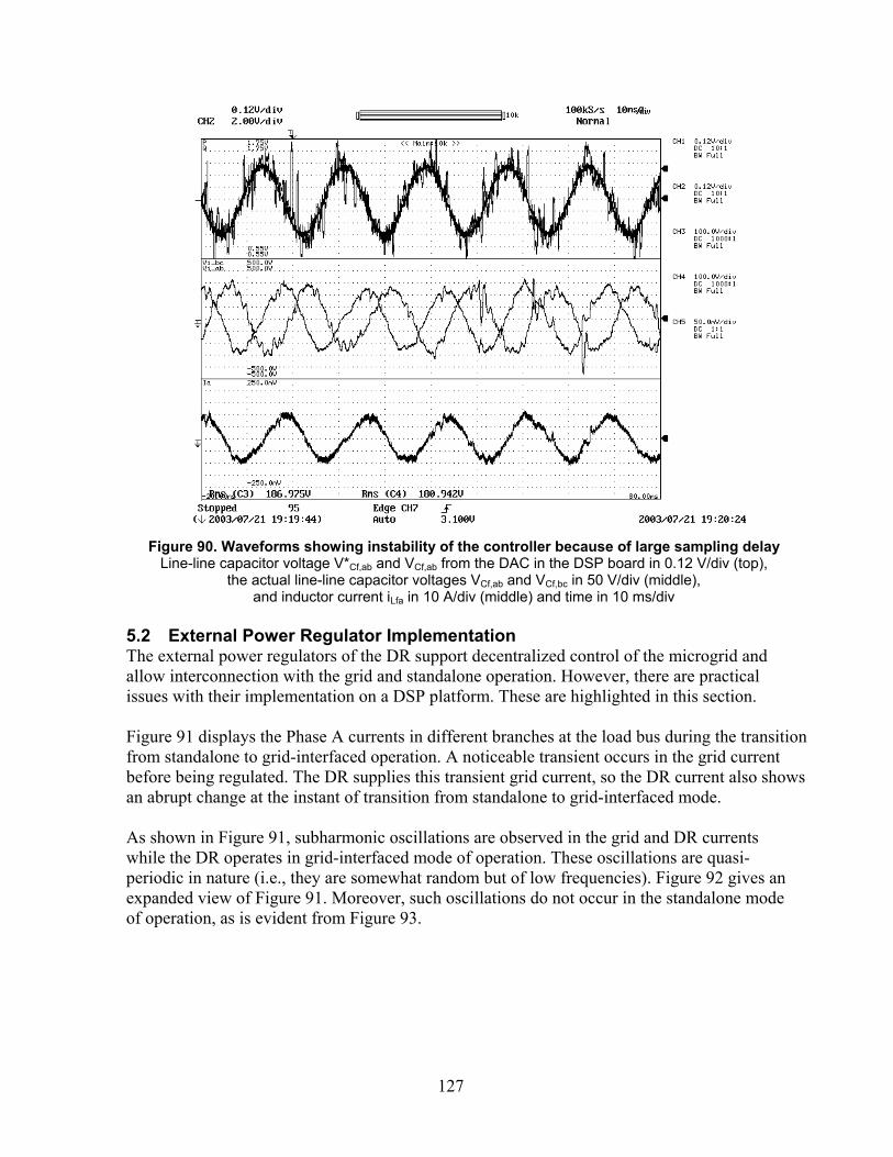
127
Figure 90. Waveforms showing instability of the controller because of large sampling delay
Line-line capacitor voltage V*Cf,ab and VCf,ab from the DAC in the DSP board in 0.12 V/div (top), the actual line-line capacitor voltages VCf,ab and VCf,bc in 50 V/div (middle),
and inductor current iLfa in 10 A/div (middle) and time in 10 ms/div 5.2 External Power Regulator Implementation The external power regulators of the DR support decentralized control of the microgrid and allow interconnection with the grid and standalone operation. However, there are practical issues with their implementation on a DSP platform. These are highlighted in this section. Figure 91 displays the Phase A currents in different branches at the load bus during the transition from standalone to grid-interfaced operation. A noticeable transient occurs in the grid current before being regulated. The DR supplies this transient grid current, so the DR current also shows an abrupt change at the instant of transition from standalone to grid-interfaced mode. As shown in Figure 91, subharmonic oscillations are observed in the grid and DR currents while the DR operates in grid-interfaced mode of operation. These oscillations are quasi-periodic in nature (i.e., they are somewhat random but of low frequencies). Figure 92 gives an expanded view of Figure 91. Moreover, such oscillations do not occur in the standalone mode of operation, as is evident from Figure 93.
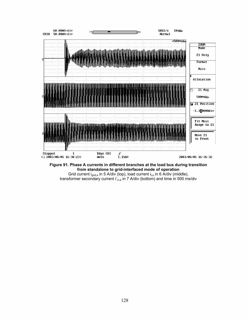
128
Figure 91. Phase A currents in different branches at the load bus during transition
from standalone to grid-interfaced mode of operation Grid current igrid,a in 5 A/div (top), load current iLa in 6 A/div (middle),
transformer secondary current i’Lt,a in 7 A/div (bottom) and time in 500 ms/div
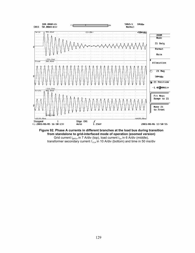
129
Figure 92. Phase A currents in different branches at the load bus during transition
from standalone to grid-interfaced mode of operation (zoomed version) Grid current igrid,a in 7 A/div (top), load current iLa in 6 A/div (middle),
transformer secondary current i’Lt,a in 10 A/div (bottom) and time in 50 ms/div

130
Figure 93. Phase A currents in different branches at the load bus
during the standalone mode of operation Grid current igrid,a in 7 A/div (top), load current iLa in 5 A/div (middle),
transformer secondary current i’Lt,a in 5 A/div (bottom) and time in 50 ms/div Further extensive tests have been conducted on the oscillatory behavior in the grid-interfaced mode of operation. Figures 94 through 96 show additional waveforms displaying the oscillatory behavior when the DR is connected with the grid. The nonlinear current in Figure 96 is due to a sizable quantity of magnetizing current of the large capacity grid transformer (Transformer T1 in Figure 7). Likely causes for such oscillatory behavior in the grid-interfaced mode are (1) quantization errors in frequency in the fixed-point implementation in the DSP, (2) the effect of sampling delay of the measured quantities on the performance of the real and reactive power regulators, (3) stability of the power regulators. Computer simulations using Electromagnetic Transients Program has confirmed these causes, and appropriate truncation schemes are being applied at present to mitigate these problems even in the presence of finite word length and sampling delays.
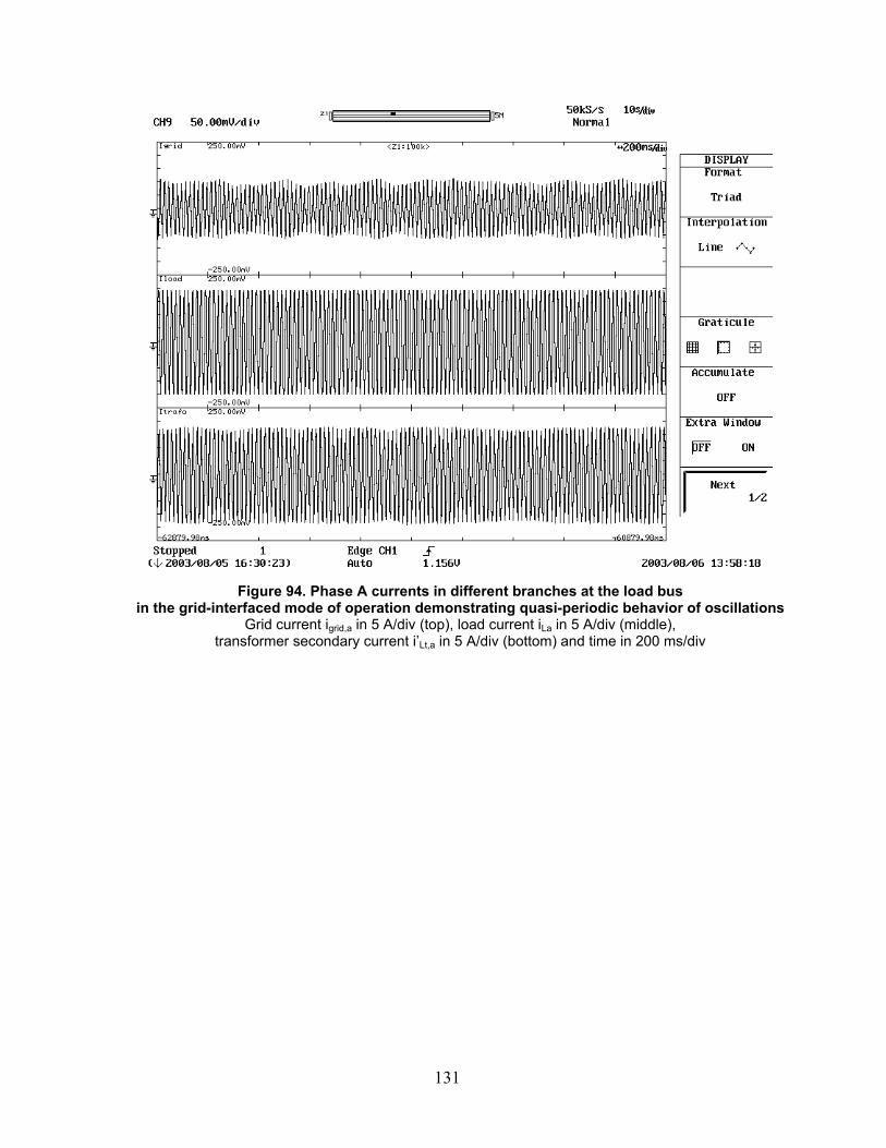
131
Figure 94. Phase A currents in different branches at the load bus
in the grid-interfaced mode of operation demonstrating quasi-periodic behavior of oscillations Grid current igrid,a in 5 A/div (top), load current iLa in 5 A/div (middle),
transformer secondary current i’Lt,a in 5 A/div (bottom) and time in 200 ms/div
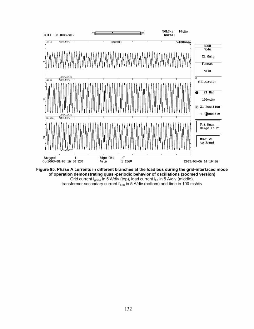
132
Figure 95. Phase A currents in different branches at the load bus during the grid-interfaced mode
of operation demonstrating quasi-periodic behavior of oscillations (zoomed version) Grid current igrid,a in 5 A/div (top), load current iLa in 5 A/div (middle),
transformer secondary current i’Lt,a in 5 A/div (bottom) and time in 100 ms/div
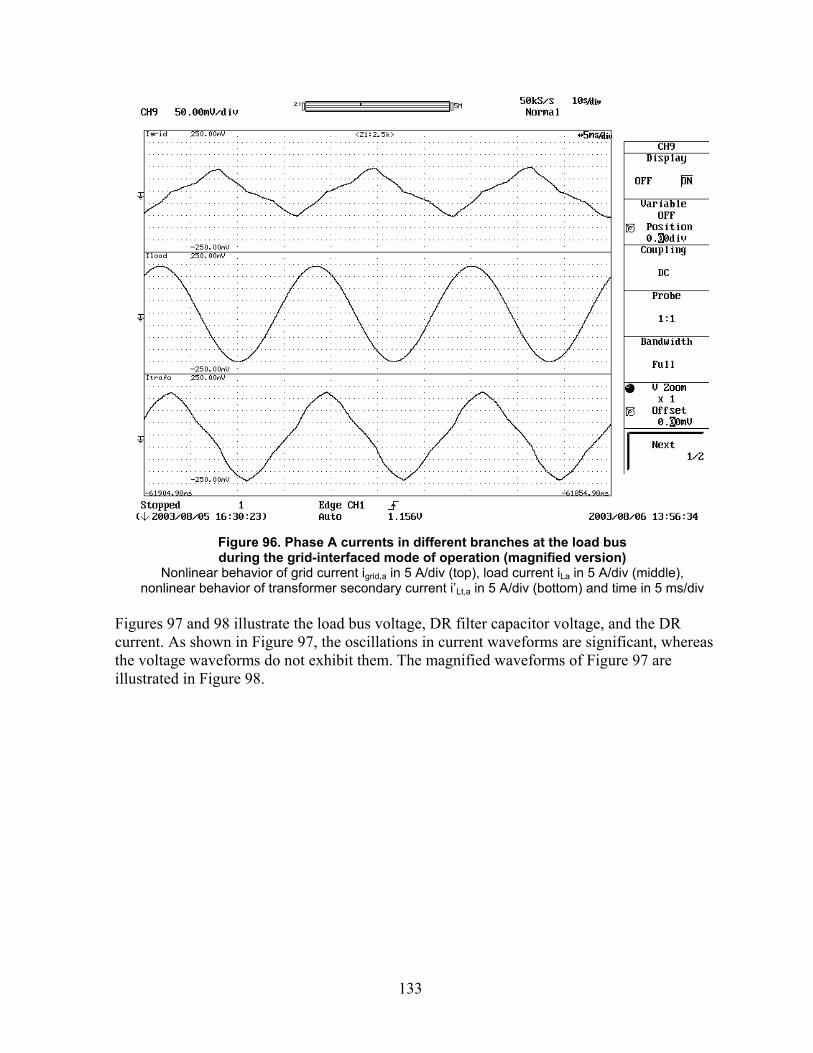
133
Figure 96. Phase A currents in different branches at the load bus during the grid-interfaced mode of operation (magnified version)
Nonlinear behavior of grid current igrid,a in 5 A/div (top), load current iLa in 5 A/div (middle), nonlinear behavior of transformer secondary current i’Lt,a in 5 A/div (bottom) and time in 5 ms/div
Figures 97 and 98 illustrate the load bus voltage, DR filter capacitor voltage, and the DR current. As shown in Figure 97, the oscillations in current waveforms are significant, whereas the voltage waveforms do not exhibit them. The magnified waveforms of Figure 97 are illustrated in Figure 98.
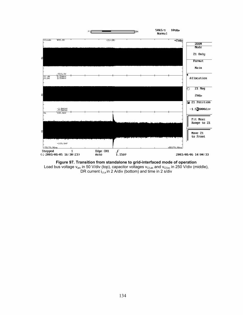
134
Figure 97. Transition from standalone to grid-interfaced mode of operation
Load bus voltage valn in 50 V/div (top), capacitor voltages vCf,ab and vCf,bc in 250 V/div (middle), DR current iLt,a in 2 A/div (bottom) and time in 2 s/div

135
Figure 98. Transition from standalone to grid-interfaced mode of operation (zoomed version)
Load bus voltage valn in 50 V/div (top), capacitor voltages vCf,ab and vCf,bc in 250 V/div (middle), DR current iLt,a in 2 A/div (bottom) and time in 10 ms/div
This chapter has highlighted some of the practical issues encountered while implementing the DR controller on a DSP platform on the laboratory-scale microgrid. Additional investigations have uncovered the causes of these problems, and an evaluation of solutions is being conducted to realize a microgrid with decentralized control and power quality conditioning capabilities.

136
6 Conclusions DR are becoming more practical as a means of supplying electrical energy generated from environmentally preferred means at a competitive cost, particularly when their heat byproduct can be readily used at the load location. Because DR typically use power electronic converters to interface with the utility/load, they have added flexibility in control. They are being considered as a valuable solution in providing power quality for sensitive load scenarios. “Power quality” refers to a variety of electromagnetic phenomena that characterize voltage and current at a given time and location on the power system [2]. Among power quality events, voltage imbalances, voltage sags, and harmonics are significant in the context of distribution systems and, hence, have been considered in this report. Loads sensitive to power quality include critical computing, data processing electronic equipment, and semiconductor fabrication machinery. Such sensitive loads demand a highly reliable power supply for a fail-safe operation. It is known that downtime of the sensitive load equipment caused by power quality events results in significant loss of revenue. Conventional approaches to solving these problems use UPS systems or backup generation systems driven by fossil fuel engines. The concept of microgrid systems has emerged more recently, unfolding new avenues in generation and distribution by improving the reliability of power delivered to sensitive/critical loads. They consist of small rated DR that are interconnected to share load demand as well as power-conditioning functions. Because the DR are small, they can be conveniently placed in proximity to the loads, thus improving the reliability of power supply. The DR, invariably, incorporate power electronic converters and are therefore capable of providing UPS functionality, power quality improvement, and energy conversion simultaneously at a reasonable cost. These features are made possible by upgrading operational and control features to enable them to become solutions to the sensitive load problem. A case study is made for designing a microgrid for an office-cum-warehouse facility. The electrical design of this facility is made to determine the location and ratings of two DR. Assuming that the system consists of three-phase balanced loads, control techniques are presented for the DR. Simulation results from Electromagnetic Transients Program software are presented to establish the efficacy of the microgrid for this case study. When power quality events take place, the DR require additional capabilities to provide reliable and well-regulated voltage to sensitive loads. This requires that power quality conditioning capabilities be incorporated in the DR controller. A control strategy is presented for the operation and control of each DR unit in the microgrid with power quality conditioning. The controller has an outer voltage loop to control the capacitor voltage and an inner current loop of the LC filter of the inverter. This helps to provide a regulated terminal voltage at the sensitive load bus even in the event of power quality disturbances. It also has an external loop for regulating the real and reactive power flow exchange between the various generators. The voltage regulation at the load bus is carried out by means of a complex controller in the stationary reference frame proposed in this report. The controller operates on three-phase complex space vector quantities that have distinct characteristics for positive and negative sequences. The positive sequence component of the three-phase complex voltage/current space

137
vector can be represented as a complex exponential with positive frequency and accordingly has a Fourier spectrum with only positive sideband. Likewise, the negative sequence component of the three-phase complex space vector has a Fourier spectrum with only a negative sideband. A multi-loop controller is designed using complex controller techniques that operate on the complex space vector quantities. Complex filter techniques have been widely applied in communications and DSP fields [32]. The complex voltage controller regulates load bus voltage even in the event of negative sequence imbalances. Frequency domain analysis techniques in the form of Bode plots are used in the design procedure. By making use of complex transfer functions, novel positive and negative sequence filters are proposed in this report. Simulation results are presented from digital simulation in Matlab SIMULINK software that establish the application of DR systems to mitigate the effects of power quality phenomena at the sensitive load bus. To operate in a microgrid, the DR are controlled by real power frequency and reactive power voltage droop characteristics. In the development of the real power frequency controller, detailed analysis is conducted on the real power speed controllers used in conventional rotating machine generators [34] as well as the real power-frequency controller employed in distributed UPS systems [36]. Because the requirements of the DR are met by the controller for the distributed UPS presented in [36], a similar controller is used for real power frequency control of the DR. These frequency and voltage droop characteristics support the decentralized operation of the DR that are interconnected in the microgrid. On similar lines, a reactive power voltage regulator has been developed and proposed in this report. Simulation results obtained from Mathematica software are presented to validate the design and performance of the real power frequency and reactive power voltage regulators. Finally, practical implementation issues encountered when testing the controllers on a DSP platform have been presented in waveforms. These waveforms have been obtained from the laboratory-scale microgrid, whose one-line schematic is illustrated in Figure 7. Investigations are continuing to study such problems and develop practical and feasible solutions to realize a microgrid with decentralized control and power quality conditioning capabilities with multiple DR units.
138
7 References [1] Sabin, D.D.; Brooks, D.L.; Sundaram, A.; Bhatt, S. "Summary of U.S. Distribution
System Power Quality Levels." International Conference on Power Quality: End-Use Applications and Perspectives Proceedings; June 1997, Stockholm, Sweden.
[2] Venkataramanan, G.; Illindala, M.S.; Houle, C.; Lasseter, R.H. "Hardware Development of a Laboratory-Scale Microgrid Phase 1 – Single Inverter in Island Mode Operation, Base Year Report: December 2000-Novermber 2001." NREL/SR-560-32527. Work performed by the Wisconsin Power Electronics Research Center, Madison, WI. Golden, CO: National Renewable Energy Laboratory. November 2002.
[3] IEEE Std 1159-1995, IEEE Recommended Practice for Monitoring Electric Power Quality.
[4] IEC Technical Committee 77, Working Group 6 (Secretariat) 110-R5, Classification of Electromagnetic Environments, Draft, January 1991.
[5] IEEE Std 141-1993, IEEE Recommended Practice for Electric Power Distribution for Industrial Plants (Red Book) (ANSI).
[6] IEEE Std 519-1992, IEEE Recommended Practices and Requirements for Harmonic Control in Electric Power Systems (ANSI).
[7] Electric Light and Power, March 1993.
[8] ITI (CBEMA) Curve Application Note, Information Technology Industry Council (ITI), Washington D.C., 2000.
[9] SEMI F47-0200, Specification for Semiconductor Processing Equipment Voltage Sag Immunity.
[10] IEEE Std 1136-1998, IEEE Recommended Practice for Evaluating Electric Power System Compatibility With Electronic Process Equipment.
[11] Douglas, J. “Power Quality Solutions,” IEEE Power Engineering Review, Vol. 14, No. 3, March 1994, pp. 3–7.
[12] Willis, H.L.; Scott, W.G. Distributed Power Generation Planning and Evaluation. New York: Marcel Dekker Inc., 2000.
[13] Illindala, M.; Venkataramanan, G. “Battery Energy Storage for Micro-Source Distributed Generation Systems.” IASTED Power and Energy Systems Conference 2002, Marina del Rey, CA.
[14] Venkataramanan, G.; Illindala, M. “Microgrids and Sensitive Loads.” IEEE Power Engineering Society Winter Meeting 2002, Vol. 1, Jan 2002, pp. 315–322.
139
[15] Illindala, M.; Venkataramanan, G. “Control of Distributed Generation Systems to Mitigate Load and Line Imbalances.” IEEE Power Electronics Specialists’ Conference 2002, Vol. 4, pp. 2013–2018.
[16] Zhang, H.; Chandorkar, M.; Venkataramanan, G. “Development of Static Switchgear for Utility Interconnection in a Microgrid.” IASTED Power and Energy Systems Conference 2003, Palm Springs, CA.
[17] Rome Cable Corp. Rome Cable Manual. Rome, NY: Rome Cable Corp., 1957.
[18] Gonen, T. Electric Power Distribution System Engineering. McGraw Hill, 1986.
[19] Novony, D.W.; Lipo, T.A. Vector Control and Dynamics of AC Drives. Oxford: Clarendon Press, 1996.
[20] Chandorkar, M.C.; Divan, D.M.; Banerjee, B. “Control of Distributed UPS Systems.” WEMPEC Report. University of Wisconsin-Madison. 94-04.
[21] Mattavelli, P.; Escobar, G.; Stankovic, A.M. “Dissipativity-Based Adaptive and Robust Control of UPS.” IEEE Transactions on Industrial Electronics; Vol. 48, No. 2, April 2001; pp. 334–343.
[22] Schauder, C.D.; Caddy, R. “Current Control of Voltage-Source Inverters for Fast Four-Quadrant Drive Performance.” IEEE Transactions on Industry Applications; Vol. IA-18, March/April 1982; pp. 163–171.
[23] Rowan, T.M.; Kerkman, R.J. “A New Synchronous Current Regulator and an Analysis of Current Regulated PWM Inverters.” IEEE Transactions on Industry Applications, Vol. IA-22, July/Aug. 1986; pp. 678–690.
[24] Briz, F.; Degner, M.W.; Lorenz, R.D. “Analysis and Design of Current Regulators Using Complex Vectors.” IEEE Transactions on Industry Applications, Vol. 36, No. 3, May/June 2000; pp. 817–825.
[25] Ryan, M.J.; Lorenz, R.D. “A High Performance Sine Wave Inverter Controller With Capacitor Current Feedback and ‘Back-EMF’ Decoupling.” IEEE Power Electronics Specialists Conference, Vol. 1, 1995, pp. 507–513.
[26] Ryan, M.J.; Brumsickle, W.E.; Lorenz, R.D. “Control Topology Options for Single-Phase UPS Inverters.” IEEE Transactions on Industry Applications, Vol. 33, No. 2, March/April 1997; pp. 493–501.
[27] Zmood, D.N.; Holmes, D.G. “Stationary Frame Current Regulation of PWM Inverters With Zero Steady-State Error.” IEEE Transactions on Power Electronics, Vol. 18, No. 3, May 2003; pp. 814–822.
140
[28] Loh, P.C.; Newman, M.J.; Zmood, D.N.; Holmes, D.G. “Improved Transient and Steady-State Voltage Regulation for Single- and Three-Phase Uninterruptible Power Supplies.” IEEE Power Electronics Specialists’ Conference 2001, Vol. 1; pp. 14–19.
[29] Mohan, N.; Undeland, T.M.; Robbins, W. Power Electronics: Converters, Applications and Design. John Wiley. 2nd edition. 1995.
[30] Hochgraf, C.G. Investigation of Multi-Level Inverter Concepts Applied to Regulation of Power System Voltages Including Imbalance. Ph.D. thesis. Univerity of Wisconsin-Madison, 1997.
[31] Yuan, X.; Merk, W.; Stemmler, H.; Allmeling, J. “Stationary Frame Generalized Integrators for Current Control of Active Power Filters With Zero Steady State Error for Current Harmonics of Concern Under Unbalanced and Distorted Operation Conditions.” IEEE Transactions on Industry Applications, Vol. 38, No. 2, March/April 2002; pp. 523–532.
[32] Venkataramanan, G.; Divan, D.M.; Jahns, T.M. “Discrete Pulse Modulation Strategies for High-Frequency Inverter Systems.” IEEE Transactions on Power Electronics, Vol. 8, No. 3, July 1993; pp. 279–287.
[33] Lang, G.R.; Bracket, P.O. “Complex Analogue Filters.” Proceedings of European Conference on Circuit Theory and Design 1981, Hague. Pp. 412–419.
[34] Bohn, C.; Atherton, D.P. “An Analysis Package Comparing PID Anti-Windup Strategies.” IEEE Control Systems Magazine, Vol. 15, No. 2, April 1995; pp. 34–40.
[35] Wood, A.J.; Wollenberg, B.F. Power Generation Operation & Control. New York: John Wiley & Sons Inc., 1984.
[36] Cohn, N. Control of Generation and Power Flow on Interconnected Power Systems. New York: John Wiley & Sons Inc., 1984.
[37] Chandorkar, M.C. Distributed Uninterruptible Power Supply Systems. Ph.D. thesis. Univerity of Wisconsin-Madison, 1995.
[38] Carpentier, J. “ ‘To Be or Not to Be Modern’ That Is the Question for Automatic Generation Control (Point of View of a Utility Engineer).” Electric Power and Energy Systems, April 1985; pp. 81–91.
[39] Jaleeli, N.; VanSlyck, L.S.; Ewart, D.N.; Fink, L.H.; Hoffmann, A.G. “Understanding Automatic Generation Control.” IEEE Transactions on Power Systems, Vol. 7, No. 3, August 1992; pp. 1106–1122.
[40] Weedy, B.M. Electric Power Systems. New York: John Wiley & Sons Inc., 1987.
[41] DSP56F805 Evaluation Module: Hardware User’s Manual. Denver, CO: Motorola Inc.

141


![U.S. Microgrid Research1].pdfU.S. Microgrid Research presentation at the University of Tokyo, Holonic Energy Systems Laboratory ... 3. fossilization and total centralization (1933-1980)](https://img.dokumen.tips/doc/110x75/5f087f457e708231d4224d93/us-microgrid-research-1pdf-us-microgrid-research-presentation-at-the-university.jpg)