Embed Size (px)
Citation preview
Hardware and Software Simulation of Transient Pulse Impact on Integrated Circuits
S.Korte, M.Camp, H.Garbe University of Hanover
Institute of Electrical Engineering and Measurement Science
D-30167 Hanover, Germany e-Mail: [email protected], [email protected], [email protected]
Abstract— In this paper the destruction effects of semiconductor devices after impact of fast transient electromagnetic pulses are investigated. Different logic devices like NANDs and Inverter were exposed to high amplitude transient pulses. The pulses have been applied as field threats and as conducted threats. Furthermore a simulation of the destruction effects with the finite element method (FEM) has been performed.
Keywords-susceptibility;semiconducter devices; electromagnetic pulse; EMP; UWB; finite element method; FEM
I. INTRODUCTION Modern electronics are of vital importance for the function of traffic systems, security systems and modern communication. A malfunction in one of these areas could cause casualties and economic disasters. Nowadays HPM and UWB equipment can be bought by everyone. Taken the aspect of electromagnetic terrorism into account an UWB system could be a very dangerous weapon, because it can be built in a very small volume due to the low energy content of the pulse. Therefore the susceptibility of electronics to pulsed electromagnetic fields like EMP and UWB pulses is of great interest. The intention of this work is to analyze the destruction effects of semiconductor devices. On that account ten different technologies (six TTL- and four CMOS-Technologies) have been tested. The pulses have been applied as field threats and as conducted threats. Upon destructions have occured the devices were opened and scanned with an electron microscope to analyze the effects which take place on the different technologies. Furthermore a simulation of the destruction effects with the finite element method (FEM) has been performed.
II. GENERAL MEASUREMENT SETUP The applied pulseshape is generally double exponential as shown in Figure 1. Five different pulse generating devices are available. Table I shows the rise time (tr) and the full width half max value (tfwhm) of the different pulses.
TABLE I. PULSE DATA
Pulse Parameters Rise time tr Pulse Length tfwhm
UWB 100 ps 2.5 ns EMP (fast) 1.5 ns 80 ns EMP (med.) 7.5 ns 180 ns UWB - slow EMP 500 ps - 10 ns 2.5 ns - 1600 ns EMP (slow) >10 ns 500 ns
Figure 1. Pulseshape and definitions
The measurements with field threats were carried out with two different waveguides. Waveguide 1 is an open area test simulator with a maximum height of about 23 m described in [1]. Waveguide 2 [2] is an open waveguide inside a shielded room enclosed by absorber walls. The absorbers at the end of the waveguide were placed on interchangeable wooden walls. The position of the septum can be adjusted via nylonthreads. The measurements of the electromagnetic properties were done by a Time Domain Reflectometer (TDR) and electric and magnetic groundplane and free field probes as described in [3]. The measurement with conducted threats were carried out with different test setups based on multiport power divider circuits using circular-sector-shaped planar components in microstrip technology described in [4] and [5].
50 %
90 %
t (s)
100 %
tr tfwhm
)()( tt eeEtE αβ −− −= 01
10 %
)( tE1
0-7803-9380-5/05/$20.00 (C) 2005 IEEE
III. DEFINITIONS
A. Failure Rates To describe the different failure effects two quantities have been defined [5]. The Breakdown Failure Rate (BFR) has been defined as the number of breakdowns of a system, divided by the number of pulses applied to it. A breakdown means no physical damage is done to the system. After a reset (self-, external- or power reset) the system is going back into function. The Destruction Failure Rate (DFR) of the device under test has been defined as the number of destructions divided by the number of pulses applied to the system. Destruction is defined as a physical damage of the system so that the system will not recover without a hardware repair.
B. Principle Behavior of BFR and DFR The BFR and DFR behaves in principle as shown in Fig. 2. As important parameters for the description of the susceptibility of a system four quantities were defined. The Breakdown Threshold (BT) specifies the value of the electrical field strength, at which the BFR gets 5% of the maximum value. The Breakdown Bandwidth (BB) is defined as the span of the electrical field strength, in which the BFR changes from 5% to 95% of the maximum. Equivalent definitions were done for the destruction failure rate DFR (compare Fig. 2).
IV. SUSCEPTIBILITY OF LOGIC-DEVICES During the investigations ten different semiconductor technologies (six TTL-, four CMOS-families) have been tested concerning the susceptibility to EMP and UWB pulses. NANDs, inverter, generic array logic devices and shift registers were chosen to observe the influence of the technology on the destruction effects.
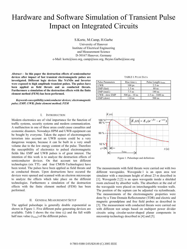
A. Test Setup To apply the different pulses to the EUT a modular setup has been realized (Fig. 3). Ten separate channels were built with a
Figure 2. BFR, DFR - principle behavior and definitions
Figure 3. NAND Test Setup – Realization
combination of differently printed circuit boards. The circuit boards were combined with ribbon cables to realize different coupling lengths at the input and output pins of the devices under test. In Fig. 3 a NAND test setup with 20 cm ribbon cable length at the input pins and ≈ 0 cm ribbon cable length at the output pins of the test devices is shown. The power supply is realized with ten different accumulators. DIP switches were implemented to the power supply unit to adjust arbitrary bit patterns at the input pins. LEDs and resistors were used as loads to observe the operating states of the devices.
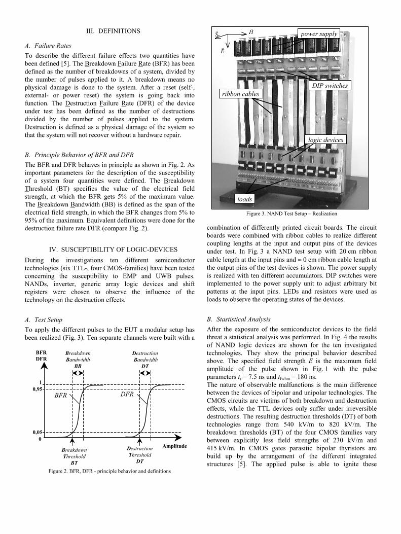
B. Stastistical Analysis After the exposure of the semiconductor devices to the field threat a statistical analysis was performed. In Fig. 4 the results of NAND logic devices are shown for the ten investigated technologies. They show the principal behavior described above. The specified field strength E is the maximum field amplitude of the pulse shown in Fig. 1 with the pulse parameters tr = 7.5 ns und tfwhm = 180 ns. The nature of observable malfunctions is the main difference between the devices of bipolar and unipolar technologies. The CMOS circuits are victims of both breakdown and destruction effects, while the TTL devices only suffer under irreversible destructions. The resulting destruction thresholds (DT) of both technologies range from 540 kV/m to 820 kV/m. The breakdown thresholds (BT) of the four CMOS families vary between explicitly less field strengths of 230 kV/m and 415 kV/m. In CMOS gates parasitic bipolar thyristors are build up by the arrangement of the different integrated structures [5]. The applied pulse is able to ignite these
ribbon cables
power supply
logic devices
loads
E
HS
DIP switches
0,95
Breakdown Threshold
BT
Breakdown Bandwidth
BB
BFR DFR
0 0,05
AmplitudeDestruction Threshold
DT
Destruction Bandwidth
DT
DFR BFR
1
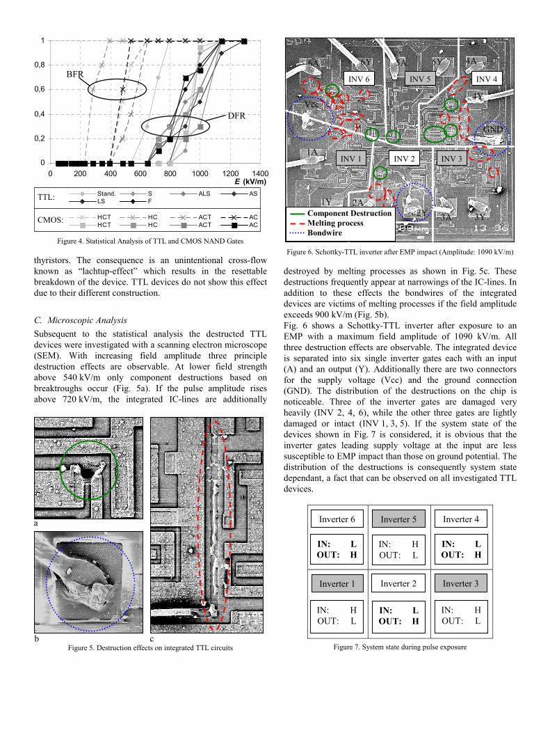
Figure 4. Statistical Analysis of TTL and CMOS NAND Gates
thyristors. The consequence is an unintentional cross-flow known as “lachtup-effect” which results in the resettable breakdown of the device. TTL devices do not show this effect due to their different construction.
C. Microscopic Analysis Subsequent to the statistical analysis the destructed TTL devices were investigated with a scanning electron microscope (SEM). With increasing field amplitude three principle destruction effects are observable. At lower field strength above 540 kV/m only component destructions based on breaktroughs occur (Fig. 5a). If the pulse amplitude rises above 720 kV/m, the integrated IC-lines are additionally
Figure 5. Destruction effects on integrated TTL circuits
Figure 6. Schottky-TTL inverter after EMP impact (Amplitude: 1090 kV/m)
destroyed by melting processes as shown in Fig. 5c. These destructions frequently appear at narrowings of the IC-lines. In addition to these effects the bondwires of the integrated devices are victims of melting processes if the field amplitude exceeds 900 kV/m (Fig. 5b). Fig. 6 shows a Schottky-TTL inverter after exposure to an EMP with a maximum field amplitude of 1090 kV/m. All three destruction effects are observable. The integrated device is separated into six single inverter gates each with an input (A) and an output (Y). Additionally there are two connectors for the supply voltage (Vcc) and the ground connection (GND). The distribution of the destructions on the chip is noticeable. Three of the inverter gates are damaged very heavily (INV 2, 4, 6), while the other three gates are lightly damaged or intact (INV 1, 3, 5). If the system state of the devices shown in Fig. 7 is considered, it is obvious that the inverter gates leading supply voltage at the input are less susceptible to EMP impact than those on ground potential. The distribution of the destructions is consequently system state dependant, a fact that can be observed on all investigated TTL devices.
Figure 7. System state during pulse exposure
a
b c
0
0,2
0,4
0,6
0,8
1
0 200 400 600 800 1000 1200 1400E (kV/m)
Stand. S ALS ASLS F i ii i i iHCT HC ACT ACHCT HC ACT AC
BFR
DFR
TTL: CMOS:
Vcc
6A 6Y 5Y 4A
4Y
GND
3Y3A 2Y 2A1Y
1A
5A
Component Destruction Melting process Bondwire
INV 1 INV 2 INV 3
INV 6 INV 5 INV 4
Inverter 6
IN: H OUT: L
IN: HOUT: L
IN: HOUT: L
IN: LOUT: H
IN: LOUT: H
IN: L OUT: H
Inverter 1 Inverter 2 Inverter 3
Inverter 4Inverter 5
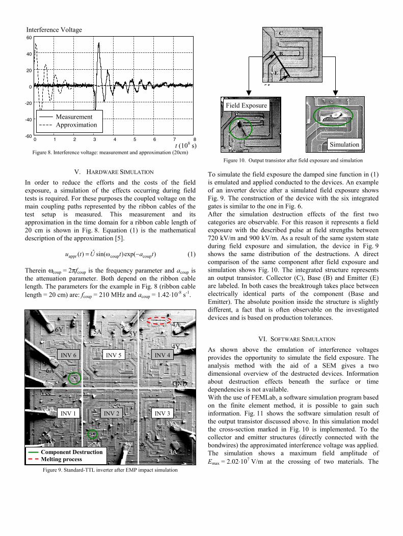
Figure 8. Interference voltage: measurement and approximation (20cm)
V. HARDWARE SIMULATION In order to reduce the efforts and the costs of the field exposure, a simulation of the effects occurring during field tests is required. For these purposes the coupled voltage on the main coupling paths represented by the ribbon cables of the test setup is measured. This measurement and its approximation in the time domain for a ribbon cable length of 20 cm is shown in Fig. 8. Equation (1) is the mathematical description of the approximation [5].
(1) Therein ωcoup = 2πfcoup is the frequency parameter and acoup is the attenuation parameter. Both depend on the ribbon cable length. The parameters for the example in Fig. 8 (ribbon cable length = 20 cm) are: fcoup = 210 MHz and acoup = 1.42⋅10-8 s-1.
Figure 9. Standard-TTL inverter after EMP impact simulation
Figure 10. Output transistor after field exposure and simulation
To simulate the field exposure the damped sine function in (1) is emulated and applied conducted to the devices. An example of an inverter device after a simulated field exposure shows Fig. 9. The construction of the device with the six integrated gates is similar to the one in Fig. 6. After the simulation destruction effects of the first two categories are observable. For this reason it represents a field exposure with the described pulse at field strengths between 720 kV/m and 900 kV/m. As a result of the same system state during field exposure and simulation, the device in Fig. 9 shows the same distribution of the destructions. A direct comparison of the same component after field exposure and simulation shows Fig. 10. The integrated structure represents an output transistor. Collector (C), Base (B) and Emitter (E) are labeled. In both cases the breaktrough takes place between electrically identical parts of the component (Base and Emitter). The absolute position inside the structure is slightly different, a fact that is often observable on the investigated devices and is based on production tolerances.
VI. SOFTWARE SIMULATION As shown above the emulation of interference voltages provides the opportunity to simulate the field exposure. The analysis method with the aid of a SEM gives a two dimensional overview of the destructed devices. Information about destruction effects beneath the surface or time dependencies is not available. With the use of FEMLab, a software simulation program based on the finite element method, it is possible to gain such information. Fig. 11 shows the software simulation result of the output transistor discussed above. In this simulation model the cross-section marked in Fig. 10 is implemented. To the collector and emitter structures (directly connected with the bondwires) the approximated interference voltage was applied. The simulation shows a maximum field amplitude of Emax = 2.02⋅107 V/m at the crossing of two materials. The
INV 1 INV 2 INV 3
INV 6 INV 5 INV 4
Component Destruction Melting process
Vcc
6A
6Y 5Y 4A
4Y
GND
3Y
3A 2Y 2A 1Y
1A
5A
Interference Voltage
0 1 2 3 4 5 6 7 8-60
-40
-20
0
20
40
60
t (108 s)
Measurement Approximation
Field Exposure
Simulation
C
B
E
)exp()ωsin(ˆ)( coupcoupappr tatUtu −=
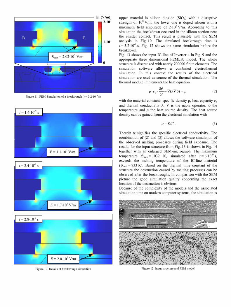
Figure 11. FEM-Simulation of a breaktrough (t = 3.2⋅10-9 s)
Figure 12. Details of breaktrough simulation
upper material is silicon dioxide (SiO2) with a disruptive strength of 108 V/m, the lower one is doped silicon with a maximum field amplitude of 2⋅107 V/m. According to this simulation the breakdown occurred in the silicon section near the emitter contact. This result is plausible with the SEM analysis in Fig. 10. The simulated breaktrough time is t = 3.2⋅10-9 s. Fig. 12 shows the same simulation before the breakdown. Fig. 13 shows the input IC-line of Inverter 4 in Fig. 9 and the
appropriate three dimensional FEMLab model. The whole structure is discretized with nearly 700000 finite elements. The simulation software allows a combined electrothermal simulation. In this context the results of the electrical simulation are used as source of the thermal simulation. The thermal module implements the heat equation
(2) with the material constants specific density ρ, heat capacity cp and thermal conductivity λ. ∇ is the nabla operator, ϑ the temperature and p the heat source density. The heat source density can be gained from the electrical simulation with
(3) Therein κ signifies the specific electrical conductivity. The combination of (2) and (3) allows the software simulation of the observed melting processes during field exposure. The results for the input structure from Fig. 13 is shown in Fig. 14 together with an enlarged SEM-micrograph. The maximum temperature ϑmax = 1032 K, simulated after t = 6⋅10-9 s, exceeds the melting temperature of the IC-line material (ϑmelt = 933 K). Based on the thermal time constant of the structure the destruction caused by melting processes can be observed after the breaktroughs. In comparison with the SEM picture the good simulation quality concerning the exact location of the destruction is obvious. Because of the complexity of the models and the associated simulation time on modern computer systems, the simulation is
Figure 13. Input structure and FEM model
pt
c =ϑ∇∇−ϑ⋅⋅ )(λδδρ p
t = 1.6⋅10-9 s
t = 2.4⋅10-9 s
t = 2.8⋅10-9 s
E = 2.0⋅107 V/m
E = 1.7⋅107 V/m
E = 1.1⋅107 V/m
Emax = 2.02⋅107 V/m
B E
E (V/m) 2⋅107
1⋅107
0
.2Ep κ=
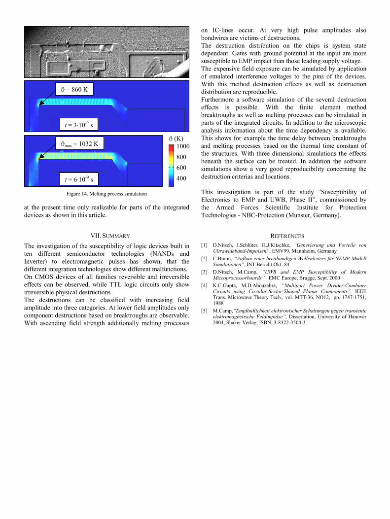
Figure 14. Melting process simulation
at the present time only realizable for parts of the integrated devices as shown in this article.
VII. SUMMARY The investigation of the susceptibility of logic devices built in ten different semiconductor technologies (NANDs and Inverter) to electromagnetic pulses has shown, that the different integration technologies show different malfunctions. On CMOS devices of all families reversible and irreversible effects can be observed, while TTL logic circuits only show irreversible physical destructions. The destructions can be classified with increasing field amplitude into three categories. At lower field amplitudes only component destructions based on breaktroughs are observable. With ascending field strength additionally melting processes
on IC-lines occur. At very high pulse amplitudes also bondwires are victims of destructions. The destruction distribution on the chips is system state dependant. Gates with ground potential at the input are more susceptible to EMP impact than those leading supply voltage. The expensive field exposure can be simulated by application of emulated interference voltages to the pins of the devices. With this method destruction effects as well as destruction distribution are reproducible. Furthermore a software simulation of the several destruction effects is possible. With the finite element method breaktroughs as well as melting processes can be simulated in parts of the integrated circuits. In addition to the microscopic analysis information about the time dependency is available. This shows for example the time delay between breaktroughs and melting processes based on the thermal time constant of the structures. With three dimensional simulations the effects beneath the surface can be treated. In addition the software simulations show a very good reproducibility concerning the destruction criterias and locations. This investigation is part of the study ”Susceptibility of Electronics to EMP and UWB, Phase II”, commissioned by the Armed Forces Scientific Institute for Protection Technologies - NBC-Protection (Munster, Germany).
REFERENCES [1] D.Nitsch, J.Schlüter, H.J.Kitschke, “Generierung und Vorteile von
Ultrawideband-Impulsen“, EMV99, Mannheim, Germany [2] C.Braun, “Aufbau eines breitbandigen Wellenleiters für NEMP Modell
Simulationen”, INT Bericht Okt. 84 [3] D.Nitsch, M.Camp, “UWB and EMP Susceptibility of Modern
Microprocessorboards”, EMC Europe, Brugge, Sept. 2000 [4] K.C.Gupta, M.D.Abouzahra, “Multiport Power Divider-Combiner
Circuits using Circular-Sector-Shaped Planar Components”, IEEE Trans. Microwave Theory Tech., vol. MTT-36, NO12, pp. 1747-1751, 1988
[5] M.Camp,“Empfindlichkeit elektronischer Schaltungen gegen transiente elektromagnetische Feldimpulse”, Dissertation, University of Hanover 2004, Shaker Verlag, ISBN: 3-8322-3504-3
ϑ (K) 1000
800
600
400
ϑmax = 1032 K
ϑ = 860 K
t = 3⋅10-9 s
t = 6⋅10-9 s