Embed Size (px)
Citation preview

GaAs, pHEMT, MMIC, 0.25 W Power Amplifier, DC to 48 GHz
Data Sheet HMC1022ACHIPS
Rev. 0 Document Feedback Information furnished by Analog Devices is believed to be accurate and reliable. However, no responsibility is assumed by Analog Devices for its use, nor for any infringements of patents or other rights of third parties that may result from its use. Specifications subject to change without notice. No license is granted by implication or otherwise under any patent or patent rights of Analog Devices. Trademarks and registered trademarks are the property of their respective owners.
One Technology Way, P.O. Box 9106, Norwood, MA 02062-9106, U.S.A.Tel: 781.329.4700 ©2019 Analog Devices, Inc. All rights reserved. Technical Support www.analog.com
FEATURES P1dB: 25 dBm (typical) at dc to 30 GHz frequency range PSAT: 26 dBm (typical) at dc to 30 GHz frequency range Gain: 11.5 dB (typical) Output IP3: 33 dBm (typical) at dc to 30 GHz frequency range Supply voltage: 10 V at 150 mA 50 Ω matched I/O Die size: 2.89 mm × 1.48 mm × 0.1 mm
APPLICATIONS Military and space Test instrumentation
FUNCTIONAL BLOCK DIAGRAM
5
1
3 4
A CG2
A CG1
RFIN
GND
2VGG2
GND
GND
RFOUT/VDD
GND
678
V GG1
A CG4
GND
A CG3
HMC1022ACHIPS
17133-001
Figure 1.
GENERAL DESCRIPTION The HMC1022ACHIPS is a gallium arsenide (GaAs), pseudomorphic high electron mobility transistor (pHEMT), monolithic microwave integrated circuit (MMIC), distributed power amplifier that operates from dc to 48 GHz. The amplifier provides 11.5 dB of small signal gain, 0.25 W (25 dBm) output power at 1 dB gain compression (P1dB), and a typical output third-order intercept (IP3) of 33 dBm, while requiring 150 mA from a 10 V supply on the VDD pin. Gain flatness is excellent from dc to 48 GHz at ±0.5 dB typical, making the
HMC1022ACHIPS ideal for military, space, and test equipment applications. The HMC1022ACHIPS also features inputs/outputs (I/Os) that are internally matched to 50 Ω, facilitating integration into multichip modules (MCMs). All data is taken with the chip connected via 0.075 mm × 0.025 mm (3 mil × 1 mil) ribbon bonds with a minimal length of 0.31 mm (12 mils).

HMC1022ACHIPS Data Sheet
Rev. 0 | Page 2 of 17
TABLE OF CONTENTS Features .............................................................................................. 1 Applications ....................................................................................... 1 Functional Block Diagram .............................................................. 1 General Description ......................................................................... 1 Revision History ............................................................................... 2 Electrical Specifications ................................................................... 3
DC to 30 GHz Frequency Range ................................................ 3 30 GHz to 40 GHz Frequency Range ......................................... 3 40 GHz to 48 GHz Frequency Range ......................................... 4
Absolute Maximum Ratings ............................................................ 5 Thermal Resistance ...................................................................... 5 ESD Caution .................................................................................. 5
Pin Configuration and Function Descriptions ..............................6 Interface Schematics .....................................................................6
Typical Performance Characteristics ..............................................7 Theory of Operation ...................................................................... 13 Applications Information .............................................................. 14
Biasing Procedures ..................................................................... 14 Mounting and Bonding Techniques for Millimeterwave GaAs MMICs ......................................................................................... 15
Outline Dimensions ....................................................................... 17 Ordering Guide .......................................................................... 17
REVISION HISTORY 1/2019—Revision 0: Initial Version
Data Sheet HMC1022ACHIPS
Rev. 0 | Page 3 of 17
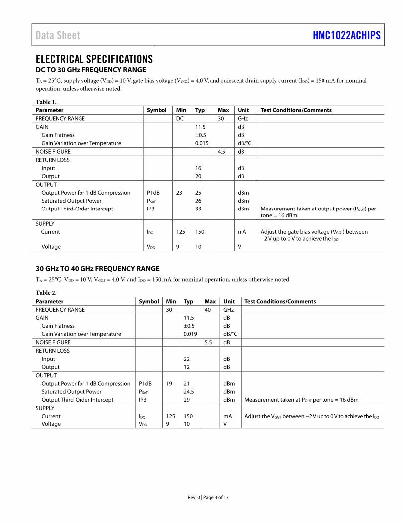
ELECTRICAL SPECIFICATIONS DC TO 30 GHz FREQUENCY RANGE TA = 25°C, supply voltage (VDD) = 10 V, gate bias voltage (VGG2) = 4.0 V, and quiescent drain supply current (IDQ) = 150 mA for nominal operation, unless otherwise noted.
Table 1. Parameter Symbol Min Typ Max Unit Test Conditions/Comments FREQUENCY RANGE DC 30 GHz GAIN 11.5 dB
Gain Flatness ±0.5 dB Gain Variation over Temperature 0.015 dB/°C
NOISE FIGURE 4.5 dB RETURN LOSS
Input 16 dB Output 20 dB
OUTPUT Output Power for 1 dB Compression P1dB 23 25 dBm Saturated Output Power PSAT 26 dBm Output Third-Order Intercept IP3 33 dBm Measurement taken at output power (POUT) per
tone = 16 dBm SUPPLY
Current IDQ 125 150 mA Adjust the gate bias voltage (VGG1) between −2 V up to 0 V to achieve the IDQ
Voltage VDD 9 10 V
30 GHz TO 40 GHz FREQUENCY RANGE TA = 25°C, VDD = 10 V, VGG2 = 4.0 V, and IDQ = 150 mA for nominal operation, unless otherwise noted.
Table 2. Parameter Symbol Min Typ Max Unit Test Conditions/Comments FREQUENCY RANGE 30 40 GHz GAIN 11.5 dB
Gain Flatness ±0.5 dB Gain Variation over Temperature 0.019 dB/°C
NOISE FIGURE 5.5 dB RETURN LOSS
Input 22 dB Output 12 dB
OUTPUT Output Power for 1 dB Compression P1dB 19 21 dBm Saturated Output Power PSAT 24.5 dBm Output Third-Order Intercept IP3 29 dBm Measurement taken at POUT per tone = 16 dBm
SUPPLY Current IDQ 125 150 mA Adjust the VGG1 between −2 V up to 0 V to achieve the IDQ Voltage VDD 9 10 V
HMC1022ACHIPS Data Sheet
Rev. 0 | Page 4 of 17
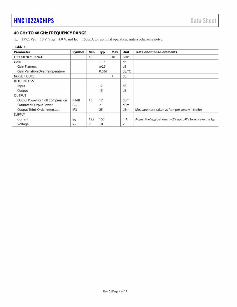
40 GHz TO 48 GHz FREQUENCY RANGE TA = 25°C, VDD = 10 V, VGG2 = 4.0 V, and IDQ = 150 mA for nominal operation, unless otherwise noted.
Table 3. Parameter Symbol Min Typ Max Unit Test Conditions/Comments FREQUENCY RANGE 40 48 GHz GAIN 11.5 dB
Gain Flatness ±0.5 dB Gain Variation Over Temperature 0.036 dB/°C
NOISE FIGURE 7 dB RETURN LOSS
Input 17 dB Output 15 dB
OUTPUT Output Power for 1 dB Compression P1dB 15 17 dBm Saturated Output Power PSAT 21 dBm Output Third-Order Intercept IP3 25 dBm Measurement taken at POUT per tone = 16 dBm
SUPPLY Current IDQ 125 150 mA Adjust the VGG1 between −2 V up to 0 V to achieve the IDQ Voltage VDD 9 10 V
Data Sheet HMC1022ACHIPS
Rev. 0 | Page 5 of 17
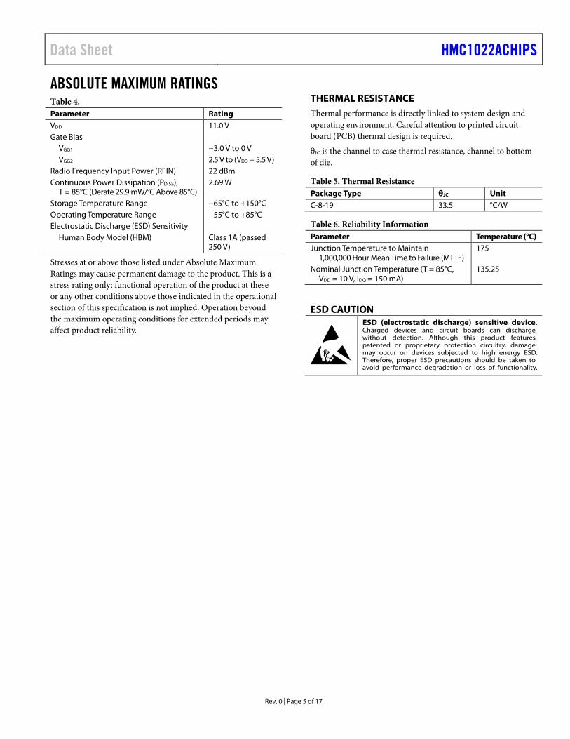
ABSOLUTE MAXIMUM RATINGS Table 4. Parameter Rating VDD 11.0 V Gate Bias
VGG1 −3.0 V to 0 V VGG2 2.5 V to (VDD − 5.5 V)
Radio Frequency Input Power (RFIN) 22 dBm Continuous Power Dissipation (PDISS),
T = 85°C (Derate 29.9 mW/°C Above 85°C) 2.69 W
Storage Temperature Range −65°C to +150°C Operating Temperature Range −55°C to +85°C Electrostatic Discharge (ESD) Sensitivity
Human Body Model (HBM) Class 1A (passed 250 V)
Stresses at or above those listed under Absolute Maximum Ratings may cause permanent damage to the product. This is a stress rating only; functional operation of the product at these or any other conditions above those indicated in the operational section of this specification is not implied. Operation beyond the maximum operating conditions for extended periods may affect product reliability.
THERMAL RESISTANCE Thermal performance is directly linked to system design and operating environment. Careful attention to printed circuit board (PCB) thermal design is required.
θJC is the channel to case thermal resistance, channel to bottom of die.
Table 5. Thermal Resistance Package Type θJC Unit C-8-19 33.5 °C/W
Table 6. Reliability Information Parameter Temperature (°C) Junction Temperature to Maintain
1,000,000 Hour Mean Time to Failure (MTTF) 175
Nominal Junction Temperature (T = 85°C, VDD = 10 V, IDQ = 150 mA)
135.25
ESD CAUTION

HMC1022ACHIPS Data Sheet
Rev. 0 | Page 6 of 17
PIN CONFIGURATION AND FUNCTION DESCRIPTIONS
5
1
3 4
A CG2
A CG1
RFIN
GND
2VGG2
GND
GND
RFOUT/VDD
GND
678
V GG1
A CG4
A CG3
HMC1022ACHIPS
GND
17133-002
Figure 2. Pad Configuration
Table 7. Pad Function Descriptions Pad No. Mnemonic Description 1 RFIN RF Input Power. This pad is dc-coupled and matched to 50 Ω. Blocking capacitor is required. See Figure 3
for the interface schematic. 2 VGG2 Gate Control 2 for the Amplifier. Attach a bypass capacitor as shown in the typical application circuit (see
Figure 47). For nominal operation, it is recommended to apply 4.0 V to VGG2. See Figure 4 for the interface schematic.
3, 4, 6, 7 ACG1, ACG2, ACG3, ACG4 Low Frequency Termination. Attach a bypass capacitor as shown in the typical application circuit (see Figure 47). See Figure 5 and Figure 6 for the interface schematics.
5 RFOUT/VDD RF Signal Output. Connect the VDD network to provide drain supply current (IDD). See Figure 47 for the typical application circuit. See Figure 5 for the interface schematic.
8 VGG1 Gate Control 1 for the Amplifier. Attach a bypass capacitor as shown in the typical application circuit (see Figure 47). Follow the MMIC Amplifier Biasing Procedure application note. See Figure 7 for the interface schematic.
Die Bottom GND Ground. Die bottom must be connected to RF and dc ground. See Figure 8 for the interface schematic.
INTERFACE SCHEMATICS
RFIN
17133-003
Figure 3. RFIN Interface Schematic
VGG2
17133-004
Figure 4. VGG2 Interface Schematic
ACG1 RFOUT/VDD
17133-005
Figure 5. ACG1 and RFOUT/VDD Interface Schematic
ACG2/ACG3/ACG4
17133-006
Figure 6. ACG2, ACG3, and ACG4 Interface Schematic
VGG1
17133-007
Figure 7. VGG1 Interface Schematic
GND
17133-008
Figure 8. GND Interface Schematic
Data Sheet HMC1022ACHIPS
Rev. 0 | Page 7 of 17
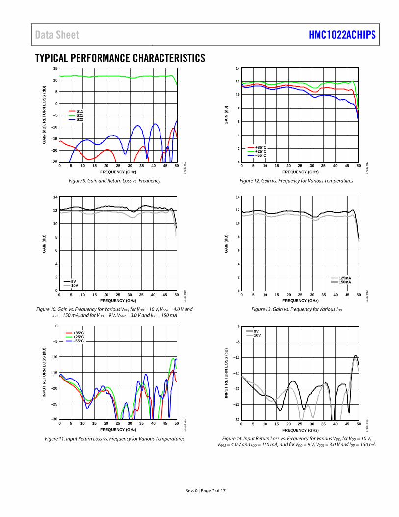
TYPICAL PERFORMANCE CHARACTERISTICS 15
–25
–20
0
–10
–5
–15
10
5
0 10 155 30 3520 25 40 45 50
GAI
N (d
B), R
ETUR
N LO
SS (d
B)
FREQUENCY (GHz)
S11S21S22
1713
3-00
9
Figure 9. Gain and Return Loss vs. Frequency
GAI
N (d
B)
FREQUENCY (GHz)
9V10V
0 10 155 30 3520 25 40 45 50
14
0
2
4
6
10
12
8
1713
3-01
0
Figure 10. Gain vs. Frequency for Various VDD, for VDD = 10 V, VGG2 = 4.0 V and
IDD = 150 mA, and for VDD = 9 V, VGG2 = 3.0 V and IDD = 150 mA
0
–30
–25
–10
–15
–20
–5
INPU
T RE
TURN
LO
SS (d
B)
FREQUENCY (GHz)
+85°C+25°C–55°C
0 10 155 30 3520 25 40 45 50
1713
3-01
1
Figure 11. Input Return Loss vs. Frequency for Various Temperatures
0 10 155 30 3520 25 40 45 50
14
0
2
4
6
10
12
8
GAI
N (d
B)
FREQUENCY (GHz)
+85°C+25°C–55°C
1713
3-01
2
Figure 12. Gain vs. Frequency for Various Temperatures
GAI
N (d
B)
FREQUENCY (GHz)
125mA150mA
0 10 155 30 3520 25 40 45 50
14
0
2
4
6
10
12
8
1713
3-01
3
Figure 13. Gain vs. Frequency for Various IDD
0
–30
–25
–10
–15
–20
–5
INPU
T RE
TURN
LO
SS (d
B)
FREQUENCY (GHz)
9V10V
0 10 155 30 3520 25 40 45 50
1713
3-01
4
Figure 14. Input Return Loss vs. Frequency for Various VDD, for VDD = 10 V,
VGG2 = 4.0 V and IDD = 150 mA, and for VDD = 9 V, VGG2 = 3.0 V and IDD = 150 mA
HMC1022ACHIPS Data Sheet
Rev. 0 | Page 8 of 17
0
–30
–25
–10
–15
–20
–5
INPU
T RE
TURN
LO
SS (d
B)
FREQUENCY (GHz)0 10 155 30 3520 25 40 45 50
125mA150mA
1713
3-01
5
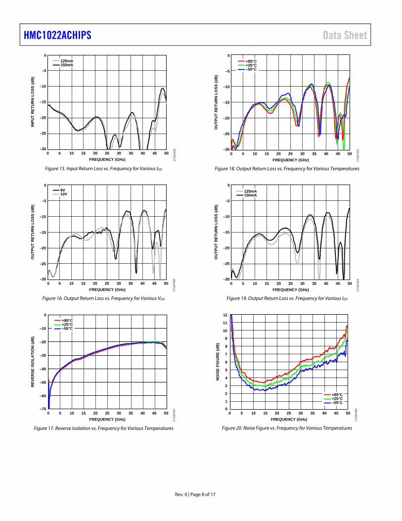
Figure 15. Input Return Loss vs. Frequency for Various IDD
OUT
PUT
RETU
RN L
OSS
(dB)
FREQUENCY (GHz)0 10 155 30 3520 25 40 45 50
0
–30
–25
–10
–15
–20
–5
9V10V
1713
3-01
6
Figure 16. Output Return Loss vs. Frequency for Various VDD
0
–70
–60
–30
–40
–50
–20
–10
REVE
RSE
ISO
LATI
ON
(dB)
FREQUENCY (GHz)
+85°C+25°C–55°C
0 10 155 30 3520 25 40 45 50
1713
3-01
7
Figure 17. Reverse Isolation vs. Frequency for Various Temperatures
OUT
PUT
RETU
RN L
OSS
(dB)
FREQUENCY (GHz)
+85°C+25°C–55°C
0 10 155 30 3520 25 40 45 50
0
–30
–25
–10
–15
–20
–5
1713
3-01
8
Figure 18. Output Return Loss vs. Frequency for Various Temperatures
OUT
PUT
RETU
RN L
OSS
(dB)
FREQUENCY (GHz)0 10 155 30 3520 25 40 45 50
0
–30
–25
–10
–15
–20
–5
125mA150mA
1713
3-01
9
Figure 19. Output Return Loss vs. Frequency for Various IDD
12
11
10
0
4
5
8
7
9
1
2
3
6
NOIS
E FI
GUR
E (d
B)
FREQUENCY (GHz)
+85°C+25°C–55°C
0 10 155 30 3520 25 40 45 50
1713
3-02
0
Figure 20. Noise Figure vs. Frequency for Various Temperatures
Data Sheet HMC1022ACHIPS
Rev. 0 | Page 9 of 17
P1dB
(dBm
)
FREQUENCY (GHz)0 10 155 30 3520 25 40 45 50
+85°C+25°C–55°C
30
25
20
0
5
15
10
1713
3-02
1
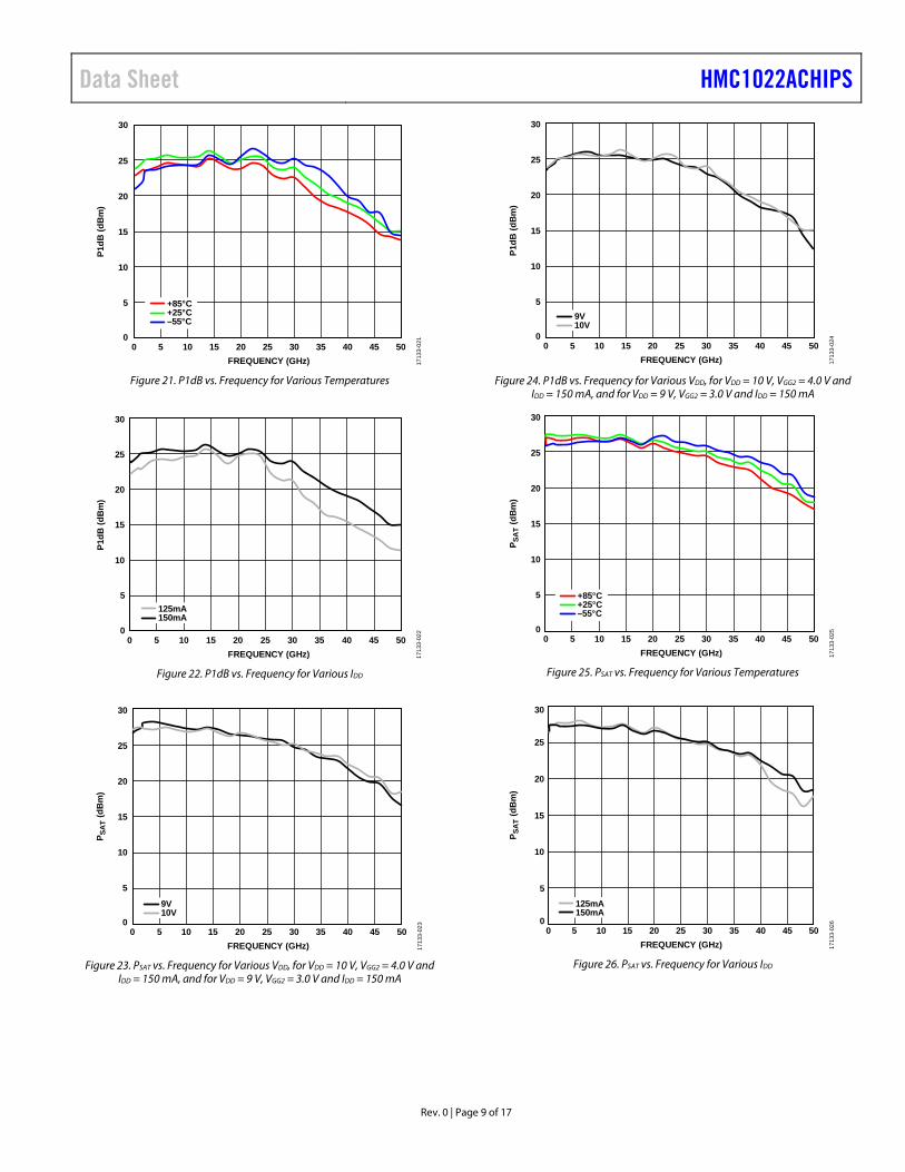
Figure 21. P1dB vs. Frequency for Various Temperatures
30
25
20
0
5
15
10
P1dB
(dBm
)
FREQUENCY (GHz)0 10 155 30 3520 25 40 45 50
125mA150mA
1713
3-02
2
Figure 22. P1dB vs. Frequency for Various IDD
P SAT
(dBm
)
FREQUENCY (GHz)
9V10V
0 10 155 30 3520 25 40 45 50
30
25
20
0
5
15
10
1713
3-02
3
Figure 23. PSAT vs. Frequency for Various VDD, for VDD = 10 V, VGG2 = 4.0 V and
IDD = 150 mA, and for VDD = 9 V, VGG2 = 3.0 V and IDD = 150 mA
P1dB
(dBm
)
FREQUENCY (GHz)
9V10V
0 10 155 30 3520 25 40 45 50
30
25
20
0
5
15
10
1713
3-02
4
Figure 24. P1dB vs. Frequency for Various VDD, for VDD = 10 V, VGG2 = 4.0 V and
IDD = 150 mA, and for VDD = 9 V, VGG2 = 3.0 V and IDD = 150 mA
0 10 155 30 3520 25 40 45 50
30
25
20
0
5
15
10
P SAT
(dBm
)
FREQUENCY (GHz)
+85°C+25°C–55°C
1713
3-02
5
Figure 25. PSAT vs. Frequency for Various Temperatures
P SAT
(dBm
)
FREQUENCY (GHz)0 10 155 30 3520 25 40 45 50
30
25
20
0
5
15
10
125mA150mA
1713
3-02
6
Figure 26. PSAT vs. Frequency for Various IDD
HMC1022ACHIPS Data Sheet
Rev. 0 | Page 10 of 17
28
00 50
PAE
(%)
FREQUENCY (GHz)
1012141618
26242220
8
2
64
10 155 30 3520 25 40 45
+85°C+25°C–55°C
1713
3-02
7
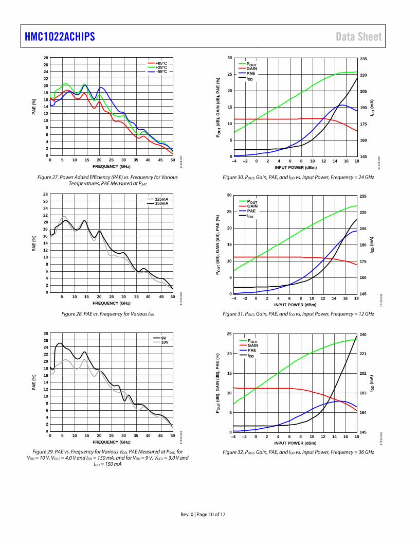
Figure 27. Power Added Efficiency (PAE) vs. Frequency for Various Temperatures, PAE Measured at PSAT
1012141618
2826242220
8
02
64
PAE
(%)
FREQUENCY (GHz)10 155 30 3520 25 40 45 50
125mA150mA
1713
3-02
8
Figure 28. PAE vs. Frequency for Various IDD
28
00 50
PAE
(%)
FREQUENCY (GHz)
1012141618
26242220
8
2
64
10 155 30 3520 25 40 45
9V10V
1713
3-02
9
Figure 29. PAE vs. Frequency for Various VDD, PAE Measured at PSAT, for
VDD = 10 V, VGG2 = 4.0 V and IDD = 150 mA, and for VDD = 9 V, VGG2 = 3.0 V and IDD = 150 mA
0
5
15
25
30
10
20
235
145
160
190
220
175
205
–4 –2 4 6 8 10 12 14 160 2 18
P OUT
(dB)
, GAI
N (d
B), P
AE (%
)
I DD
(mA)
INPUT POWER (dBm)
POUTGAINPAEIDD
1713
3-03
0
Figure 30. POUT, Gain, PAE, and IDD vs. Input Power, Frequency = 24 GHz
0
5
15
25
30
10
20
235
145
160
190
220
175
205
–4 –2 4 6 8 10 12 14 160 2 18
P OUT
(dB)
, GAI
N (d
B), P
AE (%
)
I DD
(mA)
INPUT POWER (dBm)
POUTGAINPAEIDD
1713
3-03
1
Figure 31. POUT, Gain, PAE, and IDD vs. Input Power, Frequency = 12 GHz
0
5
15
25
10
20
240
145
183
221
164
202
–4 –2 4 6 8 10 12 14 160 2 18
P OUT
(dB)
, GAI
N (d
B), P
AE (%
)
I DD
(mA)
INPUT POWER (dBm)
POUTGAINPAEIDD
1713
3-03
2
Figure 32. POUT, Gain, PAE, and IDD vs. Input Power, Frequency = 36 GHz
Data Sheet HMC1022ACHIPS
Rev. 0 | Page 11 of 17
2.4
1.0
1.6
2.0
1.2
1.4
1.8
2.2
0 2 6 10 144 8 12 16 18
POW
ER D
ISSI
PATI
ON
(W)
INPUT POWER (dBm)
6GHz12GHz18GHz24GHz30GHz36GHz42GHz
1713
3-03
3
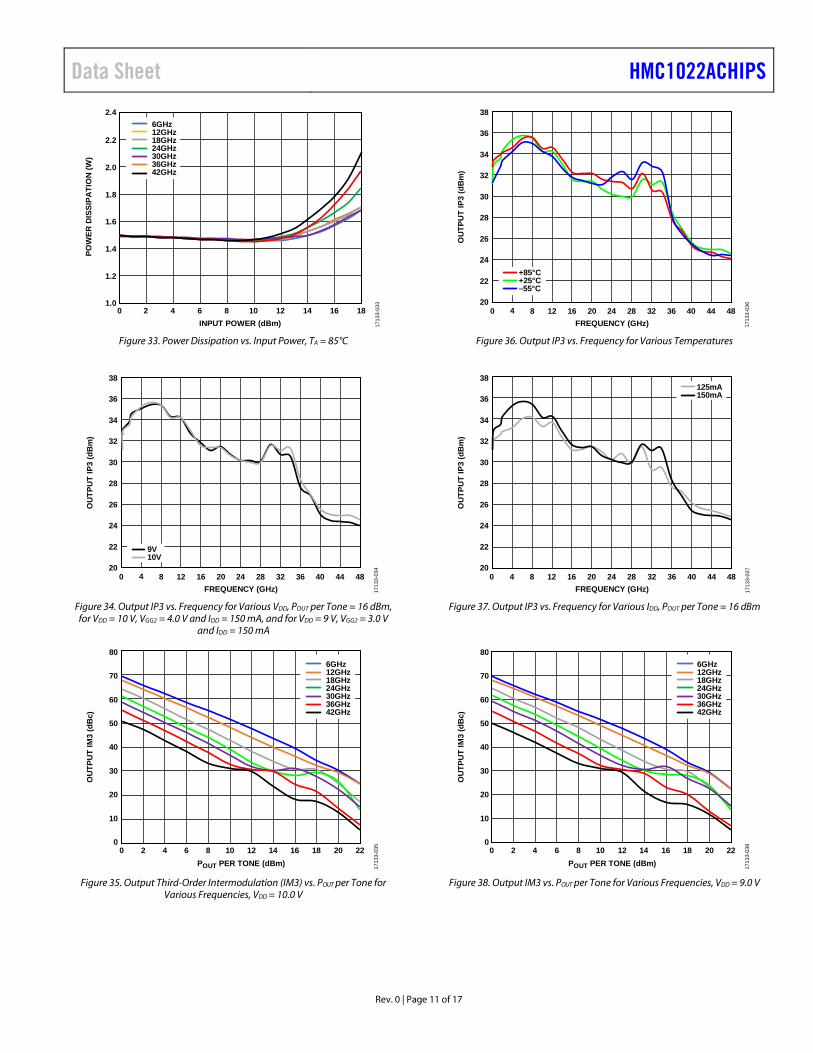
Figure 33. Power Dissipation vs. Input Power, TA = 85°C
38
20
22
30
28
36
26
24
32
34
0 4 8 24201612 28 32 36 40 44 48
OUT
PUT
IP3
(dBm
)
FREQUENCY (GHz)
9V10V
1713
3-03
4
Figure 34. Output IP3 vs. Frequency for Various VDD, POUT per Tone = 16 dBm, for VDD = 10 V, VGG2 = 4.0 V and IDD = 150 mA, and for VDD = 9 V, VGG2 = 3.0 V
and IDD = 150 mA
80
0
30
50
10
20
40
60
70
0 2 6 10 144 8 12 16 18 20 22
OUT
PUT
IM3
(dBc
)
POUT PER TONE (dBm)
6GHz12GHz18GHz24GHz30GHz36GHz42GHz
1713
3-03
5
Figure 35. Output Third-Order Intermodulation (IM3) vs. POUT per Tone for
Various Frequencies, VDD = 10.0 V
38
20
22
30
28
36
26
24
32
34
0 4 8 24201612 28 32 36 40 44 48
OUT
PUT
IP3
(dBm
)
FREQUENCY (GHz)
+85°C+25°C–55°C
1713
3-03
6
Figure 36. Output IP3 vs. Frequency for Various Temperatures
38
20
22
30
28
36
26
24
32
34
0 4 8 24201612 28 32 36 40 44 48
OUT
PUT
IP3
(dBm
)
FREQUENCY (GHz)
125mA150mA
1713
3-03
7
Figure 37. Output IP3 vs. Frequency for Various IDD, POUT per Tone = 16 dBm
80
0
30
50
10
20
40
60
70
0 2 6 10 144 8 12 16 18 20 22
OUT
PUT
IM3
(dBc
)
POUT PER TONE (dBm)
6GHz12GHz18GHz24GHz30GHz36GHz42GHz
1713
3-03
8
Figure 38. Output IM3 vs. POUT per Tone for Various Frequencies, VDD = 9.0 V
HMC1022ACHIPS Data Sheet
Rev. 0 | Page 12 of 17
250
–1.5 –0.3
QUI
ESCE
NT D
RAIN
SUP
PLY
CURR
ENT
(mA)
GATE BIAS VOLTAGE (V)
50
0
100
150
200
–1.4 –1.3 –1.2 –1.1 –1.0 –0.9 –0.8 –0.7 –0.6 –0.5 –0.4
1713
3-03
9
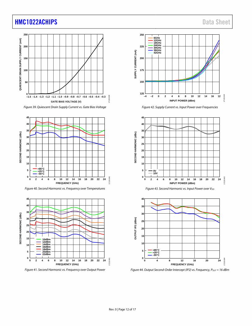
Figure 39. Quiescent Drain Supply Current vs. Gate Bias Voltage
0
5
15
45
10
20
30
35
40
25
0 4 6 8 10 12 14 162 18 20 22 24
SECO
ND H
ARM
ONI
C (d
Bc)
FREQUENCY (GHz)
+85°C+25°C–55°C
1713
3-04
0
Figure 40. Second Harmonic vs. Frequency over Temperatures
0
5
15
45
10
20
30
35
40
25
0 4 6 8 10 12 14 162 18 20 22 24
SECO
ND H
ARM
ONI
C (d
Bc)
FREQUENCY (GHz)
10dBm12dBm14dBm16dBm18dBm20dBm22dBm
1713
3-04
1
Figure 41. Second Harmonic vs. Frequency over Output Power
250
125
150
225
175
200
SUPP
LY C
URRE
NT (m
A)
INPUT POWER (dBm)
6GHz12GHz18GHz24GHz30GHz36GHz42GHz
–4 –2 0 2 4 6 8 10 12 14 16 12
1713
3-04
2
Figure 42. Supply Current vs. Input Power over Frequencies
0
5
15
45
10
20
30
35
40
25
0 4 6 8 10 12 14 162 18 20 22 24
SECO
ND H
ARM
ONI
C (d
Bc)
INPUT POWER (dBm)
9V10V
1713
3-04
3
Figure 43. Second Harmonic vs. Input Power over VDD
0
5
15
40
10
20
30
35
25
0 4 8 12 16 20 24
OUT
PUT
IP2
(dBm
)
FREQUENCY (GHz)
+85°C+25°C–55°C
1713
3-04
4
Figure 44. Output Second-Order Intercept (IP2) vs. Frequency, POUT = 16 dBm
Data Sheet HMC1022ACHIPS
Rev. 0 | Page 13 of 17
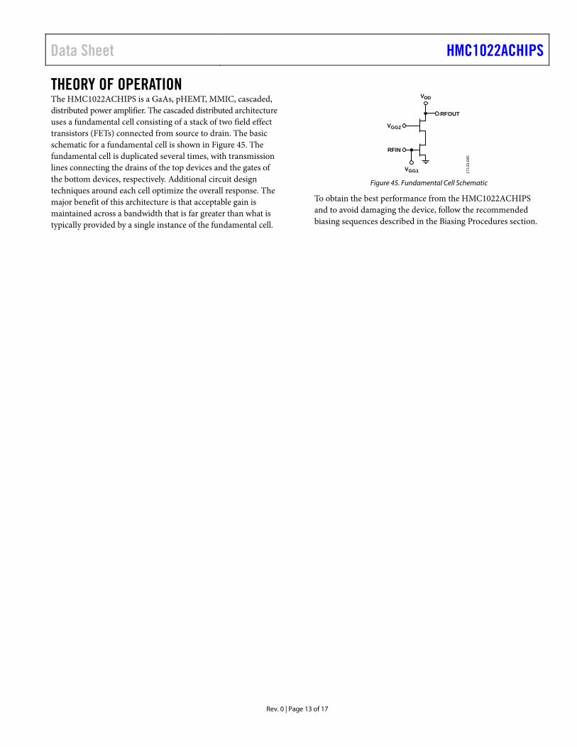
THEORY OF OPERATION The HMC1022ACHIPS is a GaAs, pHEMT, MMIC, cascaded, distributed power amplifier. The cascaded distributed architecture uses a fundamental cell consisting of a stack of two field effect transistors (FETs) connected from source to drain. The basic schematic for a fundamental cell is shown in Figure 45. The fundamental cell is duplicated several times, with transmission lines connecting the drains of the top devices and the gates of the bottom devices, respectively. Additional circuit design techniques around each cell optimize the overall response. The major benefit of this architecture is that acceptable gain is maintained across a bandwidth that is far greater than what is typically provided by a single instance of the fundamental cell.
RFOUT
VGG2
VGG1
RFIN
VDD
1713
3-04
5
Figure 45. Fundamental Cell Schematic
To obtain the best performance from the HMC1022ACHIPS and to avoid damaging the device, follow the recommended biasing sequences described in the Biasing Procedures section.
HMC1022ACHIPS Data Sheet
Rev. 0 | Page 14 of 17
APPLICATIONS INFORMATION
50ΩTRANSMISSION
LINE
3mil NOMINAL GAP
= 100pF AND 0.01µF INTEGRATED INTO ONE CASE
= 0.01µF
= 100pF
RFIN
3mil GOLD WIRE
+ –
+ –
4.7µF4.7µF
VGG1
VGG2
ACG4
ACG1
ACG2
RFOUT/VDD
ACG3
4.7µF4.7µF
1713
3-04
6
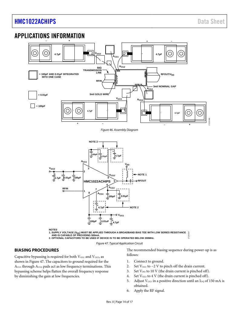
Figure 46. Assembly Diagram
4.7µF 0.01µF
0.01µF
0.01µF
100µF
100pF
100pF
+
4.7µF+
4.7µF
+
ACG1VDD
NOTE 1
NOTES1. SUPPLY VOLTAGE (VDD) MUST BE APPLIED THROUGH A BROADBAND BIAS TEE WITH LOW SERIES RESISTANCE AND IS CAPABLE OF PROVIDING 500mA.2. OPTIONAL CAPACITORS TO BE USED IF DEVICE IS TO BE OPERATED BELOW 200MHz.
RFOUT
RFIN
ACG2
ACG3
ACG4
NOTE 2
NOTE 2
VGG2
VGG1
0.01uF100pF 4.7µF
1
23
45
6
78
HMC1022ACHIPS
1713
3-04
7
Figure 47. Typical Application Circuit
BIASING PROCEDURES Capacitive bypassing is required for both VGG1 and VGG2, as shown in Figure 47. The capacitors to ground required for the ACG1 through ACG4 pads act as low frequency terminations. This bypassing scheme helps flatten the overall frequency response by diminishing the gain at low frequencies.
The recommended biasing sequence during power-up is as follows:
1. Connect to ground. 2. Set VGG1 to −2 V to pinch off the drain current. 3. Set VDD to 10 V (the drain current is pinched off). 4. Set VGG2 to 4 V (the drain current is pinched off). 5. Adjust VGG1 in a positive direction until an IDQ of 150 mA is
obtained. 6. Apply the RF signal.
Data Sheet HMC1022ACHIPS
Rev. 0 | Page 15 of 17
The recommended biasing sequence during power-down is as follows:
1. Turn off the RF signal. 2. Set VGG1 to −2 V to pinch off the drain current. 3. Set VGG2 to 0 V. 4. Set VDD to 0 V. 5. Set VGG1 to 0 V.
All measurements for the HMC1022ACHIPS are taken using the typical application circuit (see Figure 47) configured as shown in Figure 46. The bias conditions shown in the Electrical Specifications section are the operating points recommended to optimize the overall performance. Unless otherwise noted, the data shown is taken using the recommended bias conditions. Operation of the HMC1022ACHIPS at different bias conditions may provide performance that differs from what is shown in the Typical Performance Characteristics section.
MOUNTING AND BONDING TECHNIQUES FOR MILLIMETERWAVE GaAs MMICs Attach the die directly to the ground plane eutectically or with conductive epoxy (see the Handling Precautions section, the Mounting section, and the Wire Bonding section).
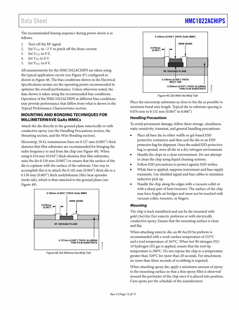
Microstrip, 50 Ω, transmission lines on 0.127 mm (0.005”) thick alumina thin film substrates are recommended for bringing the radio frequency to and from the chip (see Figure 48). When using 0.254 mm (0.010”) thick alumina thin film substrates, raise the die 0.150 mm (0.005”) to ensure that the surface of the die is coplanar with the surface of the substrate. One way to accomplish this is to attach the 0.102 mm (0.004”) thick die to a 0.150 mm (0.005”) thick molybdenum (Mo) heat spreader (moly tab), which is then attached to the ground plane (see Figure 49).
0.102mm (0.004") THICK GaAs MMIC
WIRE BOND
RF GROUND PLANE
0.127mm (0.005") THICK ALUMINATHIN FILM SUBSTRATE
0.076mm(0.003")
1713
3-04
8
Figure 48. Die Without the Moly Tab
0.254mm (0.010") THICK ALUMINATHIN FILM SUBSTRATE
0.150mm (0.005") THICKMOLY TAB
0.102mm (0.004") THICK GaAs MMIC
WIRE BOND0.076mm
(0.003")
RF GROUND PLANE
1713
3-04
9
Figure 49. Die With the Moly Tab
Place the microstrip substrates as close to the die as possible to minimize bond wire length. Typical die to substrate spacing is 0.076 mm to 0.152 mm (0.003” to 0.006”).
Handling Precautions
To avoid permanent damage, follow these storage, cleanliness, static sensitivity, transient, and general handling precautions:
Place all bare die in either waffle or gel-based ESD protective containers and then seal the die in an ESD protective bag for shipment. Once the sealed ESD protective bag is opened, store all die in a dry nitrogen environment.
Handle the chips in a clean environment. Do not attempt to clean the chip using liquid cleaning systems.
Follow ESD precautions to protect against ESD strikes. While bias is applied, suppress instrument and bias supply
transients. Use shielded signal and bias cables to minimize inductive pick up.
Handle the chip along the edges with a vacuum collet or with a sharp pair of bent tweezers. The surface of the chip may have fragile air bridges and must not be touched with vacuum collet, tweezers, or fingers.
Mounting
The chip is back metallized and can be die mounted with gold (Au)/tin (Sn) eutectic preforms or with electrically conductive epoxy. Ensure that the mounting surface is clean and flat.
When attaching eutectic die, an 80 Au/20 Sn preform is recommended with a work surface temperature of 255°C and a tool temperature of 265°C. When hot 90 nitrogen (N)/ 10 hydrogen (H) gas is applied, ensure that the tool tip temperature is 290°C. Do not expose the chip to a temperature greater than 320°C for more than 20 seconds. For attachment, no more than three seconds of scrubbing is required.
When attaching epoxy die, apply a minimum amount of epoxy to the mounting surface so that a thin epoxy fillet is observed around the perimeter of the chip once it is placed into position. Cure epoxy per the schedule of the manufacturer.

HMC1022ACHIPS Data Sheet
Rev. 0 | Page 16 of 17
Wire Bonding
RF bonds made with two 1 mil wires are recommended. Ensure that these bonds are thermosonically bonded with a force of 40 grams to 60 grams. DC bonds of a 0.001” (0.025 mm) diameter, thermosonically bonded, are recommended. Make
ball bonds with a force of 40 grams to 50 grams and wedge bonds with a force of 18 grams to 22 grams. Make all bonds with a nominal stage temperature of 150°C. Apply a minimum amount of ultrasonic energy to achieve reliable bonds. Make all bonds as short as possible, less than 12 mils (0.31 mm).

Data Sheet HMC1022ACHIPS
Rev. 0 | Page 17 of 17
OUTLINE DIMENSIONS
12-0
7-20
18-A
SIDE VIEW
1.480
0.100
*This die utilizes fragile air bridges. Any pickup tools used must not contact this area.
TOP VIEW(CIRCUIT SIDE)
2.890
1.715 0.3990.151 0.204
0.150
*AIR BRIDGEAREA
2
8
6
1
3
4
5
7
9
10111213
0.519
0.185
0.209
0.200
0.136
0.117
0.1300.186
0.723
0.272
0.191
0.199
0.103
0.200
0.190 0.204
Figure 50. 8-Pad Bare Die [CHIP]
(C-8-19) Dimensions shown in millimeters
ORDERING GUIDE Model1 Temperature Range Package Description Package Option HMC1022ACHIPS −55°C to +85°C 8-Pad Bare Die [CHIP] C-8-19 HMC1022A-SX −55°C to +85°C 8-Pad Bare Die [CHIP] C-8-19 1 The HMC1022ACHIPS model is RoHS compliant.
©2019 Analog Devices, Inc. All rights reserved. Trademarks and registered trademarks are the property of their respective owners. D17133-0-1/19(0)


![RECENT PROGRESS IN 3D/MULTILAYER MMIC ... · Web viewLow loss [10] TI / Triquint Polyimide 25 m 1 Au GaAs PHEMT Low cost, PA, LNA [11] Toshiba BCB 10 m 1 Au GaAs PHEMT MM-wave MMIC](https://img.dokumen.tips/doc/110x75/6128664f46793703e6310aec/recent-progress-in-3dmultilayer-mmic-web-view-low-loss-10-ti-triquint-polyimide.jpg)