Embed Size (px)
Citation preview

DAVID KRESS
Director of Technical Marketing
Fundamentals of Data
Converters
9/14/2016

Analog to Electronic Signal Processing
Sensor
(INPUT)Digital ProcessorAmp Converter
Actuator
(OUTPUT)Amp Converter
Analog to Electronic Signal Processing
Sensor
(INPUT)Digital ProcessorAmp Converter
Actuator
(OUTPUT)Amp Converter

Outline
►Sampled data system types
►Digitizing processes
►Data converters for measurement systems and errors
►Data converters for dynamic systems and errors
►Sampling system problems
►Structure and use of digital-analog converters
►Structure and use of analog-digital converters
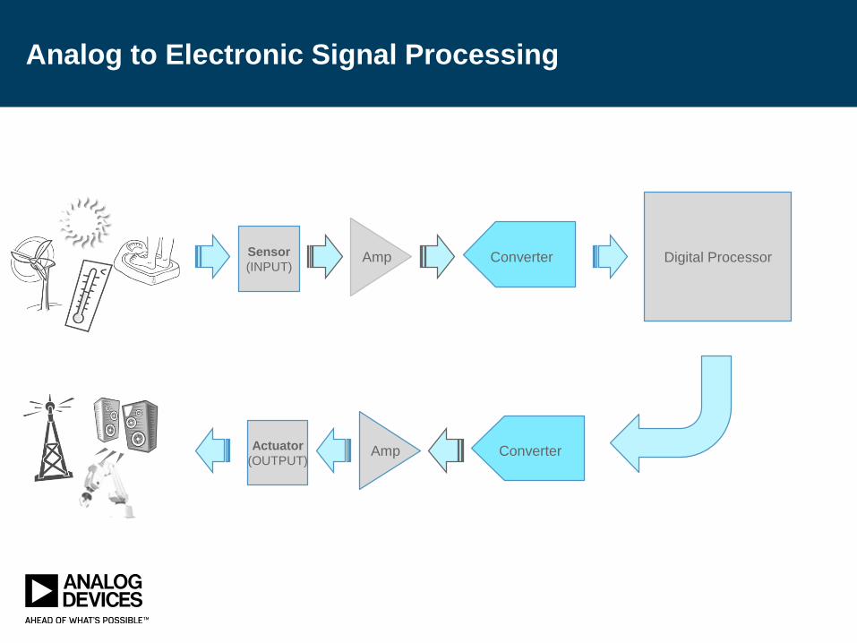
Many Types of Sampled Data Systems
►Analog to digital converters
►Digital to analog converters
►Sample and hold amplifiers
►Peak detectors
►Comparators
►Switched cap filters
►Samples a continuous signal
►Domain conversion
– Analog to digital
– Digital to analog
– Continuous time to discrete time
– Continuous frequency to
discrete frequency
►Sampling rate
– Continuous, discontinuous

Analog and Digital Domains
Why Convert to Digital?
►Analog signals are continuous and provide the entire signal
►Digital signals capture only a portion of the signal
►Why digitize?
▪ Improved signal analysis potential
▪ More robust storage
▪ More accurate transmission
►Development objective of sampled data systems is to minimize
effect of the sampling process

Sampled Data System: Sampling and Quantization
LPF
OR
BPF
N-BIT
ADCDSP
N-BIT
DAC
LPF
OR
BPF
fa
fs fs
t
AMPLITUDE
QUANTIZATION DISCRETE
TIME SAMPLING
fa
1
fsts=

Transfer Functions for Ideal 3-Bit DAC and ADC
DIGITAL INPUT
ANALOG
OUTPUT
FS
000 001 010 011 100 101 110 111 ANALOG INPUT
DIGITALOUTPUT
FS
000
001
010
011
100
101
110
111
QUANTIZATION
UNCERTAINTY
QUANTIZATION
UNCERTAINTY
DAC ADC

Unipolar Binary Code, 4-bit Converter
+15
+14
+13
+12
+11
+10
+9
+8
+7
+6
+5
+4
+3
+2
+1
0
BASE 10
NUMBERSCALE +10 V FS BINARY
1111
1110
1101
1100
1011
1010
1001
1000
0111
0110
0101
0100
0011
0010
0001
0000
9.375
8.750
8.125
7.500
6.875
6.250
5.625
5.000
4.375
3.750
3.125
2.500
1.875
1.250
0.625
0.000
+FS – 1 LSB = 15/16 FS
+7/8 FS
+13/16 FS
+3/4 FS
+11/16 FS
+5/16 FS
+9/16 FS
+1/2 FS
+7/16 FS
+3/8 FS
+5/16 FS
+1/4 FS
+3/16 FS
+1/8 FS
1 LSB = +1/16 FS
0
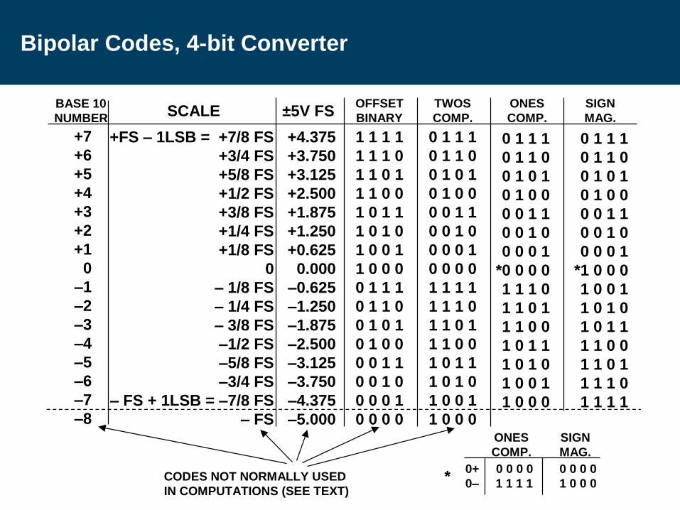
Bipolar Codes, 4-bit Converter
+4.375
+3.750
+3.125
+2.500
+1.875
+1.250
+0.625
0.000
–0.625
–1.250
–1.875
–2.500
–3.125
–3.750
–4.375
–5.000
1 1 1 1
1 1 1 0
1 1 0 1
1 1 0 0
1 0 1 1
1 0 1 0
1 0 0 1
1 0 0 0
0 1 1 1
0 1 1 0
0 1 0 1
0 1 0 0
0 0 1 1
0 0 1 0
0 0 0 1
0 0 0 0
0 1 1 1
0 1 1 0
0 1 0 1
0 1 0 0
0 0 1 1
0 0 1 0
0 0 0 1
*0 0 0 0
1 1 1 0
1 1 0 1
1 1 0 0
1 0 1 1
1 0 1 0
1 0 0 1
1 0 0 0
+FS – 1LSB = +7/8 FS
+3/4 FS
+5/8 FS
+1/2 FS
+3/8 FS
+1/4 FS
+1/8 FS
0
– 1/8 FS
– 1/4 FS
– 3/8 FS
–1/2 FS
–5/8 FS
–3/4 FS
– FS + 1LSB = –7/8 FS
– FS
±5V FSSCALE
0 1 1 1
0 1 1 0
0 1 0 1
0 1 0 0
0 0 1 1
0 0 1 0
0 0 0 1
0 0 0 0
1 1 1 1
1 1 1 0
1 1 0 1
1 1 0 0
1 0 1 1
1 0 1 0
1 0 0 1
1 0 0 0
0 1 1 1
0 1 1 0
0 1 0 1
0 1 0 0
0 0 1 1
0 0 1 0
0 0 0 1
*1 0 0 0
1 0 0 1
1 0 1 0
1 0 1 1
1 1 0 0
1 1 0 1
1 1 1 0
1 1 1 1
OFFSET
BINARY
TWOS
COMP.
ONES
COMP.
SIGN
MAG.
0+ 0 0 0 0
0– 1 1 1 1
0 0 0 0
1 0 0 0
ONES
COMP.
SIGN
MAG.
CODES NOT NORMALLY USED
IN COMPUTATIONS (SEE TEXT)
+7
+6
+5
+4
+3
+2
+1
0
–1
–2
–3
–4
–5
–6
–7
–8
BASE 10
NUMBER
*

RESOLUTION
N
2-bit
4-bit
6-bit
8-bit
10-bit
12-bit
14-bit
16-bit
18-bit
20-bit
22-bit
24-bit
2N
4
16
64
256
1,024
4,096
16,384
65,536
262,144
1,048,576
4,194,304
16,777,216
VOLTAGE
(10V FS)
2.5 V
625 mV
156 mV
39.1 mV
9.77 mV (10 mV)
2.44 mV
610 V
153 V
38 V
9.54 V (10 V)
2.38 V
596 nV*
ppm FS
250,000
62,500
15,625
3,906
977
244
61
15
4
1
0.24
0.06
% FS
25
6.25
1.56
0.39
0.098
0.024
0.0061
0.0015
0.0004
0.0001
0.000024
0.000006
dB FS
– 12
– 24
– 36
– 48
– 60
– 72
– 84
– 96
– 108
– 120
– 132
– 144
*600nV is the Johnson Noise in a 10kHz BW of a 2.2k Resistor @ 25°C
Remember: 10-bits and 10V FS yields an LSB of 10mV, 1000ppm, or 0.1%.
All other values may be calculated by powers of 2.
Quantization: The Size of a Least Significant Bit (LSB)

Practical Resolution Needs for Data Converters
► Instrumentation measurements
▪ Sensor resolution/accuracy of 0.5% = 1/200
▪ 8 bits equivalent to 1/256 -- digitizing will lose information
▪ 10x sensor resolution = 1/2000 -- 12 bits is 1/4096
▪ Allows discrimination of small changes
▪ Can also be driven by display requirements
►Dynamic signal measurements
▪ Audio systems need better than 0.1% distortion at 5% of full scale
▪ Equivalent to 1/20,000 -- 16 bits is 1/65,536

Primary Errors in Data Converters
► Instrumentation and measurement
▪ Described in LSBs(least-significant-bit), % of FS, ppm of FS
▪ Offset error – the input level needed to change the first code
▪ Gain/full-scale error – the input level need to change the last code
▪ Nonlinearity – deviation of codes from the line from zero to FS
▪ Differential nonlinearity – code-to-code deviation from 1 LSB
▪ Transition noise – ADC uncertainty in code center point

Transfer Functions for Non-Ideal 3-Bit DAC and ADC
DIGITAL INPUT
ANALOGOUTPUT
FS
000 001 010 011 100 101 110 111
NON-MONOTONIC
ANALOG INPUT
DIGITALOUTPUT
FS
000
001
010
011
100
101
110
111
MISSING CODE
DAC ADC
DIGITAL INPUT
ANALOGOUTPUT
FS
000 001 010 011 100 101 110 111
NON-MONOTONIC
DIGITAL INPUT
ANALOGOUTPUT
FS
000 001 010 011 100 101 110 111
NON-MONOTONIC
ANALOG INPUT
DIGITALOUTPUT
FS
000
001
010
011
100
101
110
111
ANALOG INPUT
DIGITALOUTPUT
FS
000
001
010
011
100
101
110
111
MISSING CODE
DAC ADC

Combined Effects of Code Transition Noise and DNL
ADC INPUT ADC INPUT ADC INPUT
CODE TRANSITION NOISE DNL TRANSITION NOISEAND DNL
ADCOUTPUT
CODE

Primary Errors in Data Converters
► Dynamic systems
► SINAD (Signal-to-Noise-and-Distortion Ratio):▪ The ratio of the rms signal amplitude to the mean value of the root-sum-
squares (RSS) of all other spectral components, including harmonics, but excluding DC.
► ENOB (Effective Number of Bits):
► SNR (Signal-to-Noise Ratio, or Signal-to-Noise Ratio Without Harmonics:▪ The ratio of the rms signal amplitude to the mean value of the root-sum-
squares (RSS) of all other spectral components, excluding the first 5 harmonics and DC
► SFDR (Spurious-Free-Dynamic-Range) Signal dynamic range in the bandwidth of interest containing no frequency noise spurs
ENOB = SINAD – 1.76dB
6.02dB

Quantization & Quantization Noise
001
010
011
100
101
110
111
1/8 2/8 3/8 4/8 5/8 6/8 7/8 FS
NORMALIZED ANALOG INPUT
DIG
ITA
L O
UT
PU
T
quantization noise error: RMS value is LSB/3.464
Quantization Error
Function

Quantization Noise as a Function of Time
t
+q
2
–q
2
SLOPE = s
+q
2s
–q
2s
e(t)
e(t) = st, –q
2s
+q
2s< t <
e2(t) = s
q –q/2s
+q/2s
(st) 2 dt = q2
12MEAN-SQUARE ERROR =
ERROR =
ROOT-MEAN-SQUARE ERROR =q
12e2(t) =

Ideal ADC Sampling
3 Different Frequencies, Sampled the Same

Ideal ADC Sampling
Once Sampled, Information is Lost
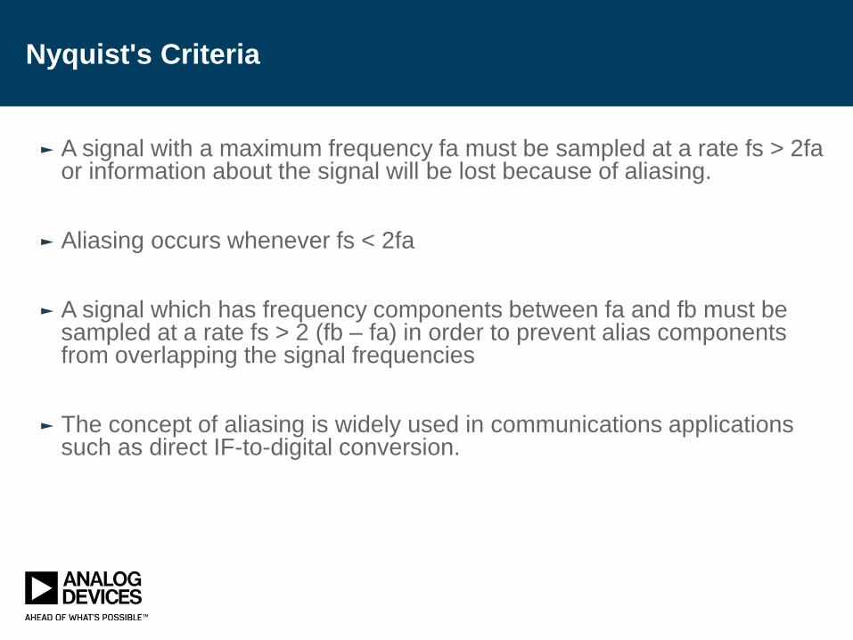
Nyquist's Criteria
► A signal with a maximum frequency fa must be sampled at a rate fs > 2fa or information about the signal will be lost because of aliasing.
► Aliasing occurs whenever fs < 2fa
► A signal which has frequency components between fa and fb must be sampled at a rate fs > 2 (fb – fa) in order to prevent alias components from overlapping the signal frequencies
► The concept of aliasing is widely used in communications applications such as direct IF-to-digital conversion.

Aliasing occurs in Many Domains
Spatial, Temporal, etc.
Image Source : Wikipedia
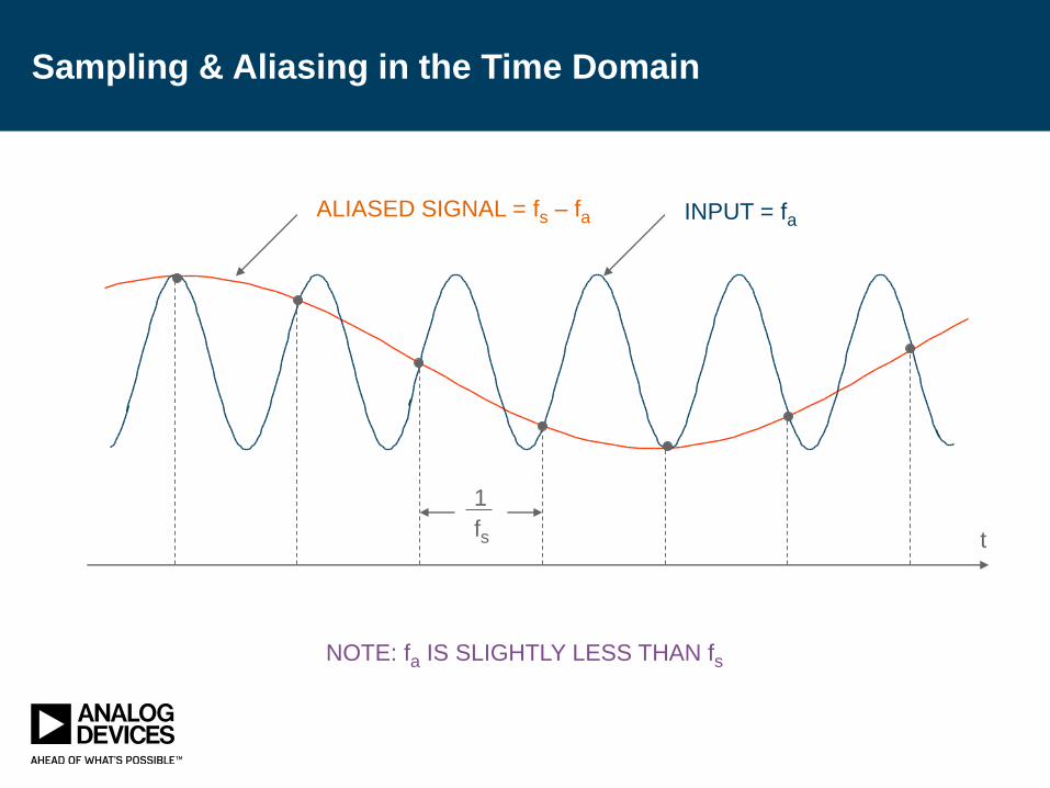
Sampling & Aliasing in the Time Domain
1
fs
INPUT = faALIASED SIGNAL = fs – fa
NOTE: fa IS SLIGHTLY LESS THAN fs
t

Baseband Antialiasing Filter Requirements
B
Kfs - fafa
KfsKfs2
STOPBAND ATTENUATION = DR
TRANSITION BAND: fa to fs - fa
CORNER FREQUENCY: fa
STOPBAND ATTENUATION = DR
TRANSITION BAND: fa to Kfs - fa
CORNER FREQUENCY: fa
Anti-Alias Filter Prevents Aliasing
Contributes to Dynamic Range
Anti-Alias Filter Objectives
➢Brick Wall (Steep/Deep Rolloff)
➢Linear Passband
➢Linear Phase
A
DR
fs
fa fs - fa
fs2
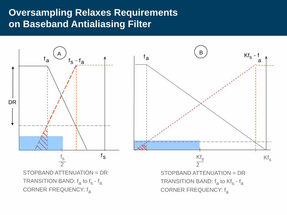
Oversampling Relaxes Requirements
on Baseband Antialiasing Filter
BA
DR
fs
fa fs - fa
Kfs - fa
fa
fs2
KfsKfs2
STOPBAND ATTENUATION = DR
TRANSITION BAND: fa to fs - fa
CORNER FREQUENCY: fa
STOPBAND ATTENUATION = DR
TRANSITION BAND: fa to Kfs - fa
CORNER FREQUENCY: fa

Sample-and-Hold Function
Required for Digitizing AC Signals
ADC
ENCODER
TIMINGSAMPLING
CLOCK
SW
CONTROL
ANALOG
INPUT
SAMPLE
HOLD
SAMPLE
C
ENCODER CONVERTS
DURING HOLD TIME
SW
CONTROL
N

Input Frequency Limitations of
Non-Sampling ADC (Encoder)
N-BIT
SAR ADC ENCODER
CONVERSION TIME = 8µs
EXAMPLE:
dv = 1 LSB = q
dt = 8µs
N = 12, 2N = 4096
fmax = 9.7 Hz
v(t) = 2N
2sin (2 f t )
dv
dt
2N
22 f cos (2 f t )=
dv
dt max= 2(N–1) 2 f
dv
dt max
2(N–1) 2 qfmax =
fs = 100 kSPS
ANALOG INPUTN
dv
dt max
q 2Nfmax =
q
q
q

Effective Aperture Delay Time
Measured with Respect to ADC Input
SAMPLING
CLOCK
ANALOG INPUT
SINEWAVE
ZERO CROSSING
+FS
-FS
0V
+te–te
te
' '
'
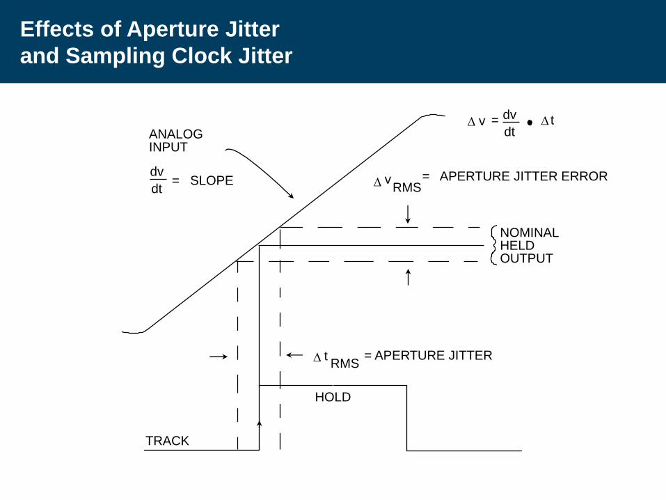
Effects of Aperture Jitter
and Sampling Clock Jitter
ANALOGINPUT
TRACK
HOLD
D
dv
dt
vdv
dt
tRMS
= APERTURE JITTER
vRMS
NOMINALHELDOUTPUT
= t
= SLOPE = APERTURE JITTER ERRORD
D
D

Theoretical SNR and ENOB Due to Jitter
vs. Fullscale Sinewave Analog Input Frequency
SNR(dB)
ENOB
100
80
60
40
20
16
14
12
10
8
6
4
1 3 10 30 100
tj = 1ns
tj = 100ps
tj = 10ps
tj = 1ps
tj = 0.1ps
120
18
FULL-SCALE SINEWAVE ANALOG INPUT FREQUENCY (MHz)
SNR = 20log 10
1
2 f t j
tj = 50fs

1-Bit DAC:
Changeover Switch (SPDT)
VREF
OUTPUT
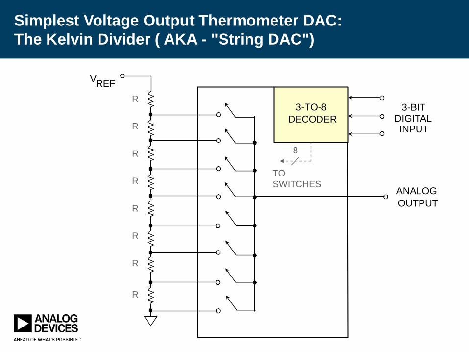
Simplest Voltage Output Thermometer DAC:
The Kelvin Divider ( AKA - "String DAC")
3-TO-8
DECODER
3-BITDIGITALINPUT
ANALOG
OUTPUT
VREF
8
TO
SWITCHES
R
R
R
R
R
R
R
R
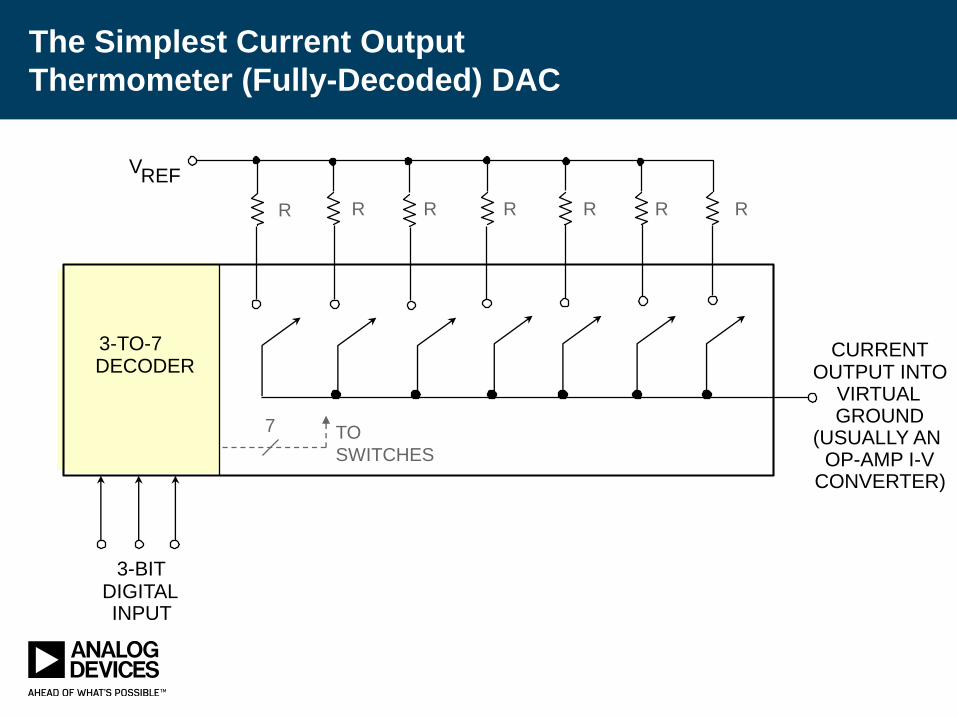
The Simplest Current Output
Thermometer (Fully-Decoded) DAC
3-BITDIGITALINPUT
CURRENTOUTPUT INTO
VIRTUALGROUND
(USUALLY ANOP-AMP I-V
CONVERTER)
VREF
3-TO-7DECODER
R R R R R R R
TO
SWITCHES
7

Voltage-Mode Binary Weighted Resistor DAC
R/8 R/4 R/2 R
V
V
REF
OUT
MSBLSB

Current-Mode R-2R Ladder Network
Resistor-Based DAC
2R
RRR
2R2R2R2R
VREF
MSB LSB
CURRENT
OUTPUTINTO
VIRTUAL
GROUND
<< R
*
* GAIN TRIM IF REQUIRED

Segmented Voltage Output DACs
KELVIN-VARLEY DIVIDER
("STRING DAC")
VREFV
REF
OUTPUT
KELVIN DIVIDER ANDR-2R LADDER NETWORK
NOTE:MSB OF R-2R LADDER
ON RIGHT
IF THE R-2R LADDER NETWORKIS MONOTONIC, THE
WHOLE DAC ISMONOTONIC
OUTPUT
(A) (B)
A
B
A
B
A
B
A
B
A
A
B A
B

Circuits from the Lab
Multiplying DAC attenuates AC signal
08
34
4-0
01
16/14-BIT
VDD
ROFS
ROFS
VOUT
RFB
RFB C82.2pF
GND
U1AD5546/AD5556
IOUT
R2R1
RCOMR1
16/14 DATA
REF
U2AD8610
–
+
C40.1µF
C51µF
C60.1µF
C71µF
+12V
–12V
WR
WR
LDAC
LDAC
RS
RS
MSB
MSB
C20.1µF
C11µF
V+
V–
+5V
+10V
VIN
–10V

Digital Potentiometer Applications
►Amplifier and other component adjustment
▪ Connect across offset-adjust pins
▪ Gain adjustment or fine tuning
►System calibration
▪ Digital pots inserted in strategic system locations
▪ System tune-up automatically or manually
▪ Non-volatile RAM setting returns on system power-up
▪ RAM can be one-time program or re-programmable
▪ Settings can be stored centrally and transmitted for system re-adjustment

Circuits from the Lab
Digital Potentiometer Gain Adjustment

1-Bit DAC:
Highly-sophisticated Digital-Audio DAC
VREF
OUTPUT

Sampled Data System: Sampling and Quantization

Sampled Data System: Sampling and Quantization

Basic ADC with External Reference
VDD
VSS
GROUND
(MAY BE INTERNALLY
CONNECTED TO VSS)
ADC
ANALOG
INPUT
VREF
DIGITAL
OUTPUT
SAMPLING
CLOCK
EOC, DATA READY, ETC.
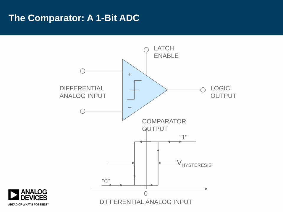
The Comparator: A 1-Bit ADC
+
–
DIFFERENTIAL
ANALOG INPUT
LOGIC
OUTPUT
LATCH
ENABLE
DIFFERENTIAL ANALOG INPUT
COMPARATOR
OUTPUT
"0"
"1"
0
VHYSTERESIS

Basic Successive Approximation ADC
(Feedback Subtraction ADC)
SHA
CONTROL
LOGIC:
SUCCESSIVE
APPROXIMATION
REGISTER
(SAR)DAC
TIMING
CONVERT
START
EOC,
DRDY,
OR BUSY
OUTPUT
ANALOG
INPUT COMPARATOR
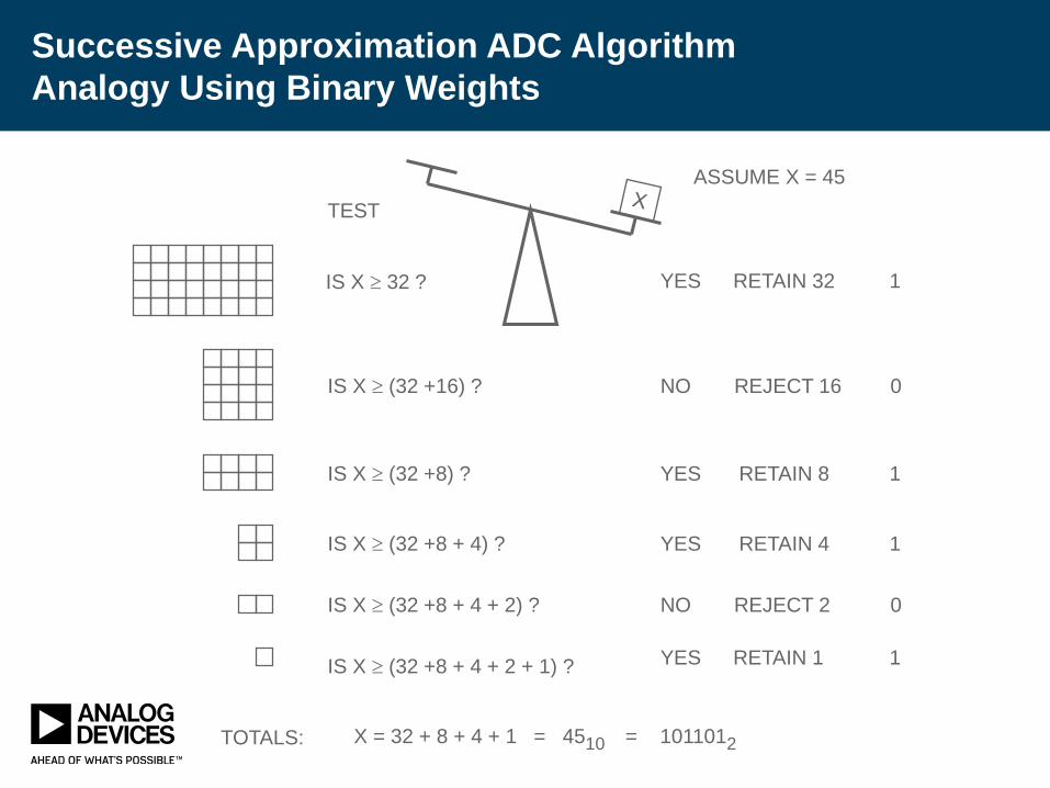
Successive Approximation ADC Algorithm
Analogy Using Binary Weights
TEST
IS X 32 ? YES RETAIN 32 1
ASSUME X = 45
IS X (32 +16) ? NO REJECT 16 0
IS X (32 +8) ? YES RETAIN 8 1
IS X (32 +8 + 4) ? YES RETAIN 4 1
IS X (32 +8 + 4 + 2) ? NO REJECT 2 0
IS X (32 +8 + 4 + 2 + 1) ? YES RETAIN 1 1
X = 32 + 8 + 4 + 1 = 4510 = 1011012TOTALS:

3-bit All-Parallel (Flash) Converter
N
R
PRIORITY
ENCODER
AND LATCH
ANALOG
INPUT
DIGITAL
OUTPUT
+VREF
R
R
R
R
R
0.5R
STROBE
1.5R
+
–
+
–
+
+
+
+
+
–
–
–
–
–

Sigma-Delta ADC - First-Order Modulator
+
_
+VREF
–VREF
DIGITAL
FILTER
AND
DECIMATOR
+
_
CLOCK
Kfs
VINN-BITS
fs
fs
A
B
1-BIT DATA
STREAM1-BIT
DAC
LATCHED
COMPARATOR
(1-BIT ADC)
1-BIT,
Kfs
SIGMA-DELTA MODULATOR
INTEGRATOR

Thank You For Watching!
View Additional Webcasts at
www.analog.com/Webcasts
Ask Questions on EngineerZone
ez.analog.com/Webcasts
Order ADI Products on Avnet
www.avnet.com