Embed Size (px)
Citation preview

FREQUENCY TRANSLATION TECHNIQUES
FOR INTERFERENCE-ROBUST
SOFTWARE-DEFINED RADIO RECEIVERS

Title: Frequency Translation Techniques for Interference-Robust Software-Defined Radio Receivers
Author: Zhiyu Ru ISBN: 978-90-365-2925-9 Copyright © 2009 by Zhiyu Ru All rights reserved. Reproduction in whole or in part is prohibited without the prior written permission of the copyright owner. PRINTED IN THE NETHERLANDS

FREQUENCY TRANSLATION TECHNIQUES FOR
INTERFERENCE-ROBUST
SOFTWARE-DEFINED RADIO RECEIVERS
DISSERTATION
to obtain the degree of doctor at the University of Twente,
on the authority of the rector magnificus, prof.dr. H. Brinksma,
on account of the decision of the graduation committee, to be publicly defended
on Thursday 12 November 2009 at 16:45
by
Zhiyu Ru
born on 8 February 1981 in Nanjing, China

This dissertation is approved by
the promotor,
prof.dr.ir. Bram Nauta
and the assistant promotor,
dr.ing. Eric A. M. Klumperink

Thank you

Committee: Chairman:
prof.dr.ir. J.H.A. de Smit Universiteit Twente Secretary:
prof.dr.ir. A.J. Mouthaan Universiteit Twente Promotor: prof.dr.ir. B. Nauta Universiteit Twente Assistant Promotor: dr.ing. E.A.M. Klumperink Universiteit Twente Members: prof.dr. J.R. Long Technische Universiteit Delft
prof.dr.ir. M. Steyaert Katholieke Universiteit Leuven prof.dr.ir. C.H. Slump Universiteit Twente
prof.ir. A.J.M. van Tuijl Universiteit Twente
VII
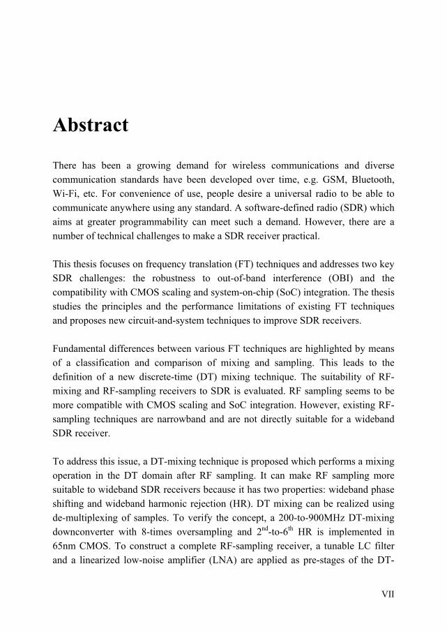
Abstract There has been a growing demand for wireless communications and diverse communication standards have been developed over time, e.g. GSM, Bluetooth, Wi-Fi, etc. For convenience of use, people desire a universal radio to be able to communicate anywhere using any standard. A software-defined radio (SDR) which aims at greater programmability can meet such a demand. However, there are a number of technical challenges to make a SDR receiver practical. This thesis focuses on frequency translation (FT) techniques and addresses two key SDR challenges: the robustness to out-of-band interference (OBI) and the compatibility with CMOS scaling and system-on-chip (SoC) integration. The thesis studies the principles and the performance limitations of existing FT techniques and proposes new circuit-and-system techniques to improve SDR receivers. Fundamental differences between various FT techniques are highlighted by means of a classification and comparison of mixing and sampling. This leads to the definition of a new discrete-time (DT) mixing technique. The suitability of RF-mixing and RF-sampling receivers to SDR is evaluated. RF sampling seems to be more compatible with CMOS scaling and SoC integration. However, existing RF-sampling techniques are narrowband and are not directly suitable for a wideband SDR receiver. To address this issue, a DT-mixing technique is proposed which performs a mixing operation in the DT domain after RF sampling. It can make RF sampling more suitable to wideband SDR receivers because it has two properties: wideband phase shifting and wideband harmonic rejection (HR). DT mixing can be realized using de-multiplexing of samples. To verify the concept, a 200-to-900MHz DT-mixing downconverter with 8-times oversampling and 2nd-to-6th HR is implemented in 65nm CMOS. To construct a complete RF-sampling receiver, a tunable LC filter and a linearized low-noise amplifier (LNA) are applied as pre-stages of the DT-

VIII
mixing downconverter. The LC filter employs an external coil and on-chip switchable capacitors. The LNA employs cascaded inverter stages linearized via an enhanced voltage mirror. The RF-sampling receiver achieves a minimum NF as low as 0.8dB and improves HR by 30dB compared to the downconverter alone. To be more robust to OBI, two FT techniques are proposed: one to improve the out-of-band linearity and the other to make the HR robust to mismatch. A low-pass blocker filtering technique is proposed to avoid voltage gain at radio frequencies (RF) but make voltage gain only at baseband simultaneously with low-pass filtering to attenuate OBI. The low voltage gain at RF is realized by means of a low “mix-impedance”, which is analyzed quantitatively. A 2-stage polyphase HR technique is proposed to perform HR in cascaded stages to dramatically improve the amplitude accuracy. To also achieve the high phase accuracy, a simple and accurate frequency divider is presented. The effects of random amplitude and phase errors to HR are analyzed. To demonstrate these concepts, a 65nm CMOS receiver based on RF mixing shows +3.5dBm in-band IIP3 and +16dBm out-of-band IIP3. More than 60dB HR ratio is measured over 40 randomly-selected chips. The multiphase clock generator works up to 0.9GHz while the -3dB RF bandwidth is measured up to 6GHz.

IX
Contents Abstract VII
1 Introduction 1
1.1 Software(-Defined) Radio: Motivation and Origins……..……….…....…1 1.2 Challenges……………………..…………………………….……………5 1.3 State of the Art………………….…………………………………….…12
1.3.1 Wideband Receivers…………….……………………….………...13 1.3.2 Robustness to Out-of-Band Interference…..……………………....16 1.3.3 Flexible Baseband Channel Selection………………………......…20 1.3.4 Compatibility with CMOS Scaling and SoC Integration.................21
1.4 Research Objectives…………………………….…………………....….21 1.5 Thesis Organization………………………………….….…………...….22 1.6 References……………………………………...………..……………....24
2 Frequency Translation Fundamentals 29
2.1 Why Frequency Translation………………………….…………………30 2.2 Classification of Downconversion Techniques……….……………...…33 2.3 Fundamental Distinctions between Mixing and Sampling Principles…..35
2.3.1 Time Domain: Information Rate Changes or Not?..........................35 2.3.2 Frequency Domain: Frequency Translation Happens or Not?.........36
2.4 Receiver Architectures for SDR………………………………….……..38 2.4.1 Receiver Architectures………………….…………………..……..39 2.4.2 Suitability to SDR……………………….…………………..…….40

X
2.5 Challenges of RF Sampling for Wideband Receivers……….…….……45 2.5.1 Frequency-Dependent Phase Shift…………………….……..……46 2.5.2 Aliasing of Noise and Interference……………………...……..50 2.5.3 Frequency-Dependent Conversion Gain of Charge Sampling….....52
2.6 Conclusions……………………………………………..…………..…...65 2.7 References………………………………………………..……………...67
3 Discrete-Time Mixing Receiver for RF-Sampling SDR 71
3.1 Introduction…………………………………………..……………..…...71 3.2 Discrete-Time Mixing Receiver Concept…………….……………..…..72
3.2.1 Wideband Quadrature Demodulation…………….………….……73 3.2.2 Wideband Harmonic Rejection……………..……..………………76
3.3 Proof-of-Concept Implementation………………...…….………………78 3.3.1 Receiver Architecture…………………..………..………………...79 3.3.2 Circuit Implementation………………….………..……………….81
3.4 Experimental Results………………………….………..………………90 3.4.1 Conversion Gain and Noise Figure……….……...….…………….90 3.4.2 Harmonic Rejection……..…………………...……………………94 3.4.3 Performance Summary……………………….……………………96
3.5 Conclusions……………………………………………………………...98 3.6 References………………………………………..……………………...98
4 Filter and Amplifier Techniques for Interference Robustness 101
4.1 Introduction……………………………………………..………..…….101 4.2 RF-Sampling Receiver Architecture……………………..…………….104 4.3 Digitally-Controlled LC Filter………………………....………………105
4.3.1 Filter Concept…………………………………..…..…………….105 4.3.2 Implementation………………………………….……..………...109
4.4 Amplifier based on Enhanced Voltage Mirror.……….……….………113 4.4.1 LNA Topology…………………………………..…….…………113 4.4.2 Mechanism of Nonlinearity Compensation……….……..………117

XI
4.5 Experimental Results…………………………………….…………….120 4.5.1 Filter Response, Gain, NF and HR…………………..…….……..121 4.5.2 Linearity…………………………………..……………….……..124
4.6 Conclusions……………………………………..………………..…….126 4.7 References………………………………………..…………………….127
5 Downconversion Techniques Robust to Out-of-Band Interference 129
5.1 Introduction……………………………………..……………..……….130 5.2 Low-Pass Blocker Filtering…………………….……………..……….131
5.2.1 Concept…………………………………….……………..……...132 5.2.2 Realization…………………………………..……………..……..134
5.3 2-stage Polyphase Harmonic Rejection………….……..……………...136 5.3.1 Block Diagram……………………………..…….………………137 5.3.2 Working Principle…………………………..…….……………...138
5.4 Chip Implementation……………………………...…………………...142 5.4.1 Linear LNTA……………………………………………………..143 5.4.2 Passive Mixer…………………………………………………….146 5.4.3 Accurate Multiphase Clock………………………………………147 5.4.4 High-Swing TIA………………………………...….…………….151 5.4.5 Baseband R-net………………………………..…..……………..154
5.5 Receiver Frequency Range Extension……………….……..………….154 5.6 Experimental Results…………………………………………………..157
5.6.1 Gain, NF, in-band IIP2/IIP3, and RF bandwidth.………..………158 5.6.2 Out-of-Band IIP2/IIP3………………………..………….………160 5.6.3 1dB Compression Point and Blocker Filtering………….……….161 5.6.4 Harmonic Rejection…………………………….…..……………163 5.6.5 Performance Summary and Benchmark………………………….165
5.7 Conclusions…………………………………………………………….167 5.8 References………………………………………..…………………….168

XII
6 Conclusions 171 6.1 Summary and Conclusions…………………….…………..…………..171 6.2 Original Contributions……………………….……………..………….176 6.3 Future Work………………………………....……………..………….179 6.4 References………………………………………..…………………….181
A Analysis of the “Mix-Impedance” 183
A.1 Derivation………………………………………..…………...…………183 A.1.1 Impedance without Spectrum Shift……….....……………………185 A.1.2 Impedance with Spectrum Shift………….……………………….188 A.2 Simulation……...…………………………..……………………………190 A.3 References……..……………………………………………….……….195
B Effect of Random Amplitude and Phase Errors to Harmonic Rejection 197
B.1 Derivation………………………………………………...…….……….197 B.2 Simulation………………………………………………..……..……….199 B.3 References……………………………………….……………..………..201
Acknowledgements 203
Samenvatting 205
Publications 207
About the Author 209

1
Chapter 1 Introduction Wireless communications rely on radio. Future wireless communications rely on software-defined radio (SDR), which makes radio more flexible. However, a low-cost practical SDR still stays as a concept so far. This thesis addresses the main challenges of realizing practical SDR receivers, focusing on the analog front-end. Section 1.1 describes the motivation behind the trend towards SDR and the actual origins of the concept of software radio and software-defined radio. From the concept to a practical SDR, a few major challenges exist. Section 1.2 discusses these challenges and Section 1.3 reviews the up-to-date solutions. After that, Section 1.4 defines the objectives of this work. Then Section 1.5 gives an overview on the organization of this thesis. Section 1.6 provides the references of the chapter. 1.1 Software(-Defined) Radio: Motivation and Origins Communication is essential for people, and the modern society heavily relies on it. Assisted by wireless technologies, people can communicate over long distances, flexibly at different places, and even while moving. Today, radio communication not just exists but it is everywhere and keeps growing. As a typical example, by 2008, the global mobile phone penetration rate was already more than 50% and it is predicted to reach 75% by 2011 [1]. In the mean time, different communication standards have been developed to serve various applications in our daily life. To give a couple of examples, in the spectrum of 400MHz to 6GHz (Fig. 1.1) which is typically used for mobile applications, we

Chapter 1 Introduction
2
Figure 1.1 An example of spectrum allocation for mobile communications have the cellular standards GSM, UMTS, and LTE, the wireless networking standards Wi-Fi and WiMAX, the mobile TV standard DVB-H, the navigation standard GPS, and the short-range communication standards Bluetooth and RFID, etc. The list is only getting longer as new standards are still emerging. For convenience of use, it is a natural step to combine as many applications as possible into a single mobile radio device, i.e. to add more functionality. Compared to the approach of adding separate radio hardware for every application, the use of flexible hardware controlled by software can make the device smaller, lighter, more flexible, and at lower cost. This trend of radio evolution, i.e. moving functionality into software for a flexible multi-function radio device, leads to the emerging of the term “software radio” (SWR), coined in the early 90’s by Mitola [2] [3]. Similar trends can be seen in many other electronic systems.
With radio functions mainly implemented in software, SWR refers to a universal radio platform being able to cope with current and future communication standards only by running and upgrading different software. The goal of SWR is to make a radio as flexible as a computer: the software defines the application. However, a SWR receiver has to first convert an analog radio signal into a digital representation before the signal can be handled by software. Consequently, an analog-to-digital converter (ADC) is indispensible. As shown in Fig. 1.2, an ideal SWR receiver [4] [5] moves the ADC towards the antenna, through an anti-aliasing filter. Such a radio concept can be very flexible because it minimizes the analog hardware and maximizes the usage of digital hardware which provides the platform to run software.

1.1 Software(-Defined) Radio: Motivation and Origins
3
Figure 1.2 Ideal software-radio (SWR) receiver but impractical yet
The dominant technology for digital circuits is CMOS which stands for Complementary Metal-Oxide Semiconductor. Moreover, commercially it is attractive to achieve a high level of integration for a low cost, and the trend is clear: system-on-chip (SoC), with both analog and digital implemented on the same chip. Therefore, SWR hardware is preferably implemented in CMOS. As mentioned, an ideal SWR receiver requires a high-performance ADC to directly digitize RF signal. However, without downconversion and filtering ahead, the required ADC performance such as speed and dynamic range is usually impractical in CMOS. For example, assuming at least 10GS/s speed and 16-bit resolution are required to receive RF signals up to 5GHz, and assuming 1pJ/conversion for the ADC lead to almost 1kW power consumption, if feasible at all [6]. While Mitola described the ideal SWR receiver has an ADC connected closely to antenna, he also suggested that a practical SWR receiver may have the ADC located at IF after frequency conversion [2]-[5]. Such a practical SWR is close to another term “software-defined radio” (SDR), which, according to Mitola [5, Section II-A], was defined by BellSouth [7] in 1995 “to describe an evolution towards greater programmability of a wireless infrastructure” [5]. The implementation of a SDR (can be but) does not have to be primarily in software like a SWR, but at least the function of a SDR can be defined, or reconfigured, by software for different communication standards, preferably also software-upgradable to deal with future standards. Please note that there is not necessarily to be a clear boundary between SDR and non-SDR; the more programmable the better. Today’s industrial multi-band multi-mode radios can be seen as an intermediate step towards SDR.

Chapter 1 Introduction
4
Figure 1.3 Conceived phase space of radio evolution towards greater programmability
Besides coping with multiple standards, SDR can also be an enabler for cognitive radio (CR) [8]. A CR can automatically adapt its parameters, such as carrier frequency, dynamic range, and power consumption, in response to the radio environment and user demands. The present cognitive radio application regulated by FCC [9] focuses on dynamic spectrum access in the unoccupied TV band below 1GHz, which is aimed to improve the efficiency of utilizing the scarce spectrum resources.
Till this end, we have presented the motivation of SWR and SDR as well as the actual origins of these two terms which were not always clear. However, the relationship between them can still be confusing and these two terms can be mixed up with each other. To further clarify the ambiguity between them as well as to clearly set our research scope, we summarize, in our view, their distinctions below. Functionally, both are flexible radios but SWR also restricts the way of implementation to be primarily in software, i.e. SWR = software-intensive SDR. In our view, the scope of SDR is broader and includes SWR, while SWR represents the highest degree of flexibility in SDR. Our research targets at SDR, which is broader and more feasible for now.

1.2 Challenges
5
Figure 1.4 A typical block diagram of a traditional receiver Fig. 1.3 represents, in our view, a conceived phase space of radio evolution towards greater programmability. It also indicates the scope of traditional radio, multi-band radio, SWR, and SDR, concerning the diversity of radio function and the way to implement radio function. Note that software has to run on hardware, but a SWR uses less hardware and more software, in percentage of the construction of a radio function, than traditional single-band radio and today’s multi-band radio. SDR is a wide research topic, which can range from analog to digital and from transmitter to receiver. As for SWR, the preferred technology for SDR is also CMOS, for the sake of SoC integration. For the feasibility of A/D conversion in CMOS, till this age we still need functions such as amplification, downconversion, and filtering in the analog front-end (AFE) of a radio receiver before A/D conversion. This thesis focuses on the analog front-end for SDR receivers in CMOS, aiming at low power consumption to target mobile applications. There are several main challenges to realize such an AFE, which will be discussed in the next section.
1.2 Challenges
Fig. 1.4 shows the typical block diagram of a traditional receiver, which is often dedicated to one band for one standard. The analog front-end (AFE) consists of an RF band-selection filter (pre-filter), low-noise amplifier (LNA), mixer, baseband channel-selection filter (CSF), and variable-gain amplifier (VGA). The challenges we talk about here will be focused on the AFE, while the synthesizer and ADC are

Chapter 1 Introduction
6
outside the scope of this thesis. We may also want to receive more than one standard at the same time, which can be challenging too but not in the scope of this thesis. The key difference of a SDR receiver compared to a traditional receiver is the enhanced flexibility, i.e. it is functionally more flexible. To turn a traditional radio receiver into a flexible SDR receiver, considering the two main purposes of SDR, i.e. multi-standard and cognitive radio applications, we face at least the following challenges in the AFE:
a) To deliver “good enough” NF and in-band linearity to satisfy each targeted
standard in a continuously-covered wide frequency range; b) To provide “good enough” linearity or selectivity tunable over a wide
frequency range, against strong out-of-band interference; c) To realize channel-selection filtering which can cover variable channel
bandwidth, e.g. in small steps, with reconfigurable filter order; d) To be compatible with CMOS scaling and SoC integration.
Generally, all the above goals should better be achieved with low cost, small size, and low power consumption for large-volume (consumer) mobile applications. To clarify their meanings, we will discuss each point of the listed challenges.
Points a) and b)
Points a) and b) deal with NF and linearity, which are key performance to radio receivers, and for SDR receivers, the considerations for noise and linearity are quite different from traditional radios. For a specific band of one standard, we may classify the received RF signal into three categories: desired signal, in-band interference (IBI), and out-of-band interference (OBI). The desired signal is often a single channel in a band and IBI refers to signals in other channels than the desired in the same band while OBI refers to signals in any other bands. As an example, Fig. 1.5 shows a typical interference scenario for the GSM standard in the 900MHz band [11], indicating a

1.2 Challenges
7
Figure 1.5 A typical blocking scenario for GSM 900MHz standard
weak desired signal at -99dBm (3dB above the sensitivity level), IBI as strong as -23dBm and OBI as strong as 0dBm. First let’s look at the desired signal. For each standard, there is a sensitivity level to define the minimum available power of the desired signal received at antenna. For instance, the required sensitivity for GSM is -102dBm over a 200kHz channel while that number for DVB-H is -98dBm over a 5MHz channel. A traditional receiver should be able to provide good enough NF in a specific frequency band to satisfy the minimum signal-to-noise ratio (SNR) for successful demodulation when antenna signal is at the sensitivity level. Since a SDR receiver should cover multiple standards, it should be able to meet the required sensitivity for each individual standard in different bands. Furthermore, to accommodate future standards and for CR applications, it is preferred that SDR can cover a wide bandwidth continuously. As most mobile communication standards up to now use a band between 400MHz and 6GHz (Fig. 1.1), our focus will be on this frequency range. Typically, a NF < 6dB should be “good enough” for most standards in this RF range [12]. Now let’s look at interference. Traditional wireless standards use dedicated radio bands, so that in-band interference (IBI) can be distinguished from out-of-band interference (OBI). For a SDR aiming at covering arbitrary frequencies, the definition of IBI and OBI may become fuzzy. Still, we will use the terms IBI and OBI in this thesis as: 1) current SDR receivers often aim at covering multiple traditional radio standards which
Chapter 1 Introduction
8
have clear band definitions; 2) even if this is not the case, e.g. for cognitive radios, a SDR still aims at implementing selectivity, i.e. receive a signal for which the baseband bandwidth is much smaller than the RF carrier frequency. In the latter case OBI can be interpreted as “out-of-baseband interference”. For mobile communications, the IBI can be as strong as -30 to -20dBm while the OBI can be as strong as -10 to 0dBm [13]. An RF pre-filter is often employed to suppress the OBI to no larger than the IBI level. Since a desired band is often a small ratio of its carrier frequency and strong interference can be close to the desired signal frequency, the RF pre-filters often require high quality factor (Q) and sharp roll-off. Such filters are difficult to integrate on chip and are typically dedicated to one specific band, e.g. SAW band filters. As the RF pre-filters often do not suppress the IBI, the linearity of the receiver should be good enough to tolerate IBI. A receiver in-band IIP3 > -10dBm would be “good enough” for most standards [12] [26]. As shown in Fig. 1.4, assisted by a dedicated RF pre-filter, a traditional receiver should be able to provide good enough linearity to counter the IBI and the suppressed OBI. However, for SDR receivers, using a dedicated filter for each band would dramatically increase the size and cost. Therefore we prefer a flexible RF pre-filter, which can adjust its center frequency, bandwidth, and order for different standards. Such a filter can attenuate the OBI for each standard so that the required linearity of the SDR receiver is relaxed. However, to build such a filter at low cost is very challenging, since it usually requires multiple poles and zeros simultaneously tunable over a broadband, on top of the requirements of a traditional dedicated RF pre-filter such as high Q, sharp roll-off, and low insertion loss. Research on flexible RF pre-filters is actively ongoing, e.g. exploring the use of MEMS technology [14]. In this thesis, we look at solutions from the CMOS receiver perspective. In parallel to enhance the filter flexibility to relax the receiver linearity, we can also try to enhance the linearity of the receiver so that the requirements on the filter can be relaxed. After all, what matters is that the combined efforts from both sides, filter and receiver, meet the required system specification. Since pre-filters mainly suppress OBI, to relax those filters, the robustness of the SDR receiver to OBI is critical, while the required in-band linearity is similar to traditional receivers for each standard.

1.2 Challenges
9
Figure 1.6 Wideband interfering mechanisms: (a) out-of-band nonlinearity; (b) harmonic mixing
At least two mechanisms generate in-band distortion due to OBI: 1) nonlinearity related mixing of strong out-of-band interferers via, e.g., intermodulation or cross-modulation; 2) harmonic mixing of interferers with LO harmonics due to hard-switching mixers or the use of digital LO waveforms. To clarify, we will explain these two mechanisms briefly below.
1) Out-of-band nonlinearity: Nonlinearity may generate intermodulation and harmonic distortion falling on top of the desired signal, or may desensitize a receiver due to blockers and produce cross modulation [15]. Fig. 1.6 (a)

Chapter 1 Introduction
10
shows an example, where a wideband LNA amplifies the desired signal at 0.8GHz and the undesired wideband interference at 1.6GHz and 2.4GHz with an equal gain of 20dB1. At the output of the LNA, the amplified interference challenges the nonlinear output impedance of the LNA and the linearity of a next-stage mixer, which can severely degrade the signal-to-noise-and-distortion ratio. Without sufficient RF pre-filtering, the out-of-band linearity can become the bottleneck since OBI is much stronger than IBI. For example, if OBI is 20dB stronger than IBI, without any attenuation of OBI, the required out-of-band IIP3 can be derived as 30dB higher than the required in-band IIP3, if aiming at that OBI generates the same distortion level as IBI.
2) Harmonic mixing: Linear time-variant behavior in a hard-switching mixer, or
equivalently multiplication with a square wave, down-converts not only the desired signal but also interference around LO harmonics. Fig. 1.6 (b) shows an example, where both the desired signal at 0.8GHz and the interference at 2.4GHz pass through the wideband LNA with equal gain. Even if the LNA is perfectly linear, the interference may directly fall on top of the desired signal after the mixer via the 3rd-order harmonic mixing. A quick calculation shows that large rejection ratio is wanted: if we want to bring harmonic responses down to the noise floor (e.g. -100dBm in 10MHz for NF=4dB), and cope with interferers between -40 and 0dBm, a harmonic rejection ratio of 60 to 100dB is needed.
Both out-of-band nonlinearity and harmonic mixing can severely degrade signal-to-distortion ratio 2 which directly affects the demodulation of desired signal. Therefore, in our view, a SDR receiver is not just a wideband receiver with “good enough” NF and in-band linearity, but it should also have enhanced out-of-band linearity and harmonic rejection (HR).
1 The gain might be lower for a clipping signal. 2 Signal-to-Distortion Ratio is so important to software-defined radio that it can be viewed as another interpretation of “SDR”.

1.2 Challenges
11
Point c)
Channel selection is used to select the desired channel and so to reduce the required dynamic range for the ADC. It is often done at baseband where high selectivity can be achieved more easily than at RF. For a traditional receiver, a fixed baseband filter to meet one dedicated standard is good enough. But for a SDR receiver, the channel-selection filter should be able to vary its characteristics, e.g. bandwidth and order, to fit the requirements of different standards. For a true SDR receiver, the filter is expected to cover a range of channel bandwidth in a certain resolution, suitable for both current and future standards. Later we will see through a couple of examples that some promising solutions have been proposed for SDR channel-selection filters.
Point d)
The achievable system performance can directly depend on the adopted technology platform. For example, it might be easier for technologies such as superconductor or GaAs than CMOS to achieve wider bandwidth and higher dynamic range, which are key parameters to realize the AFE of a SDR receiver. However, as described in Section 1.1, we prefer to implement SDR in CMOS as an ideal technology platform for software, and integrate analog and digital systems on one chip. Unfortunately, CMOS downscaling mainly benefits digital circuits but can put extra-ordinary challenges for analog circuits [10]. Although SoC integration may bring the opportunity of digitally-assisted calibration for analog blocks, it is challenging to integrate analog with digital on the same chip due to, e.g., simultaneous switching noise generated from millions of digital gates. Therefore, it is challenging to make SDR compatible with CMOS scaling and suitable for SoC integration. Now we may summarize the major challenges of the analog front-end (AFE) of a SDR receiver, compared to a traditional receiver, as:
SDR Receiver AFE = Wideband Receiver AFE +
Robustness to Out-of-band Interference + Flexible Channel-Selection Filtering +
Compatibility with CMOS Scaling and SoC Integration.

Chapter 1 Introduction
12
Figure 1.7 An integrated quad-band GPRS/EDGE transceiver [16]
1.3 State of the Art This section presents state-of-the-art work3 related to SDR receivers, as a brief literature overview. The aims are: a) to show how the challenges pointed out in the previous section have been addressed so far by other researchers; b) to show the differences and the added values of our work (Chapter 2 to 5) compared to others’.
A traditional multi-standard receiver basically puts multiple dedicated receivers in parallel with each for one band. It is effective now for product development aiming at a quick time to market and low risk. However, this approach significantly increases system size and cost for every band that is added, for both on-chip and off-chip components. It is becoming increasingly impractical as there are already a large number of radio communication standards, while new ones are continuously being developed.
3 Please note that most work mentioned in this section is not “previous” work but developed in parallel to this Ph.D. project which got started in 2005. Of course, they are only valid to be “state-of-the-art” till 2009 when the thesis is written.
1.3 State of the Art
13
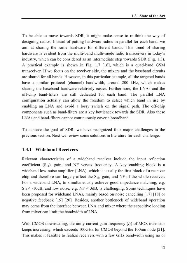
To be able to move towards SDR, it might make sense to re-think the way of designing radios. Instead of putting hardware radios in parallel for each band, we aim at sharing the same hardware for different bands. This trend of sharing hardware is evident from the multi-band multi-mode radio transceivers in today’s industry, which can be considered as an intermediate step towards SDR (Fig. 1.3). A practical example is shown in Fig. 1.7 [16], which is a quad-band GSM transceiver. If we focus on the receiver side, the mixers and the baseband circuits are shared for all bands. However, in this particular example, all the targeted bands have a similar protocol (channel) bandwidth, around 200 kHz, which makes sharing the baseband hardware relatively easier. Furthermore, the LNAs and the off-chip band-filters are still dedicated for each band. The parallel LNA configuration actually can allow the freedom to select which band in use by enabling an LNA and avoid a lossy switch on the signal path. The off-chip components such as band-filters are a key bottleneck towards the SDR. Also these LNAs and band-filters cannot continuously cover a broadband. To achieve the goal of SDR, we have recognized four major challenges in the previous section. Next we review some solutions in literature for each challenge.
1.3.1 Wideband Receivers
Relevant characteristics of a wideband receiver include the input reflection coefficient (S11), gain, and NF versus frequency. A key enabling block is a wideband low-noise amplifier (LNA), which is usually the first block of a receiver chip and therefore can largely affect the S11, gain, and NF of the whole receiver. For a wideband LNA, to simultaneously achieve good impedance matching, e.g. S11 < -10dB, and low noise, e.g. NF < 3dB, is challenging. Some techniques have been proposed for wideband LNAs, mainly based on noise cancelling [17] [18] or negative feedback [19] [20]. Besides, another bottleneck of wideband operation may come from the interface between LNA and mixer where the capacitive loading from mixer can limit the bandwidth of LNA. With CMOS downscaling, the unity current-gain frequency (fT) of MOS transistor keeps increasing, which exceeds 100GHz for CMOS beyond the 100nm node [21]. This makes it feasible to realize receivers with a few GHz bandwidth using no or

Chapter 1 Introduction
14
very few inductors which cost area. In recent years, many wideband receivers have come up, partly enabled by the process advancement. They can continuously cover a wide bandwidth, say at least an octave, and therefore largely share the receiver components. These features differentiate them from the current industrial multi-band multi-mode radios (Fig. 1.7).
One of the first CMOS wideband receivers was published in 2004 [22], showing a -3dB bandwidth of 200MHz to 2.2GHz and implemented in 0.18μm technology. It is a zero-IF receiver employing noise-cancelling LNA and passive mixer. By an extensive use of high effective gate-source voltages (VGS-VTH) and resistive degeneration, it achieves +1dBm IIP3 at a conversion gain of around 25dB. However, this comes at the cost of a relatively high NF of 7dB and a power consumption of 200mW. The UCLA SDR receiver [23] published in 2006 is a zero-IF receiver aming at the 800MHz to 5GHz range in 90nm CMOS, including baseband filters and an LO generator. The noise-cancelling LNA exploits inductive peaking to extend the bandwidth at the input and the interface with mixer and a passive mixer is adopted for low 1/f noise and high IIP2. The LNA and the mixer operate at a 2.5V supply for high dynamic range, consuming 45mW. At a full-gain setting, the LNA and mixer achieves 30dB gain, 5dB NF, and -15dBm IIP3 up to 2.4GHz, while at a medium-gain setting, it achieves 21dB gain, 9dB NF, and -3.5dBm IIP3. However, the performance of the whole receiver is only presented for two frequencies: 900MHz and 2.4GHz. No measurement data are shown beyond 2.4GHz. The IMEC SDR transceiver [24] [25] published in 2007 consists of a zero-IF wideband receiver in 0.13μm CMOS. The publications stress on extensive programmability aiming at an adaptive power/performance trade-off. To resolve the conflict of low 1/f noise required below 500MHz RF and fast transistors required for 5GHz, two separate LNAs are used: a noise-cancelling LNA for 100MHz to 2.5GHz and an inductive-degeneration LNA for 2.5GHz to 6GHz. Its second generation [26] published in 2009 is a 0.1-to-5GHz zero-IF receiver implemented in 45nm CMOS, including baseband filter and frequency synthesizer. A passive mixer follows two LNAs, an active-feedback LNA for 0.1GHz to 1.5GHz and a resistive-feedback LNA for 1.5GHz to 5GHz. The dual-band LNAs use switchable low-Q inductive peaking to cover the whole wide band in four sub-

1.3 State of the Art
15
bands. The receiver sensitivity is verified for 6 different standards, from DVB-H at 600MHz to 802.11n at 5GHz, achieving an NF from 2.3dB to 6.5dB. In parallel to [24-26], a similar approach of realizing a SDR transceiver aiming at a power/performance trade-off has also been developed in industry. As an example, the Bitwave “Softransceiver” [27] is configurable from 700MHz to 3.8GHz and is compliant with cellular, WLAN, and broadcast standards. Each element of the transceiver’s single-component transmit and receive chain can be software-optimized for a given standard. The receiver integrates an analog front-end, ADCs and frequency synthesizers, in 0.13μm CMOS. However, detailed performance data such as NF and linearity are not available. Besides, many wideband receivers have been developed for ultra-wideband (UWB) applications [28] [29]. Some of their techniques can also be useful to SDR. The “Blixer” [30] published in 2008 is a wideband zero-IF receiver using a combined balun-LNA-I/Q-mixer topology. It stacks an I/Q current-commutating mixer on top of a noise-canceling balun-LNA, thus reusing the bias current. The real part of the impedance of all RF nodes is kept low, and the voltage gain is not created at RF but at baseband where capacitive loading is no problem. Thus the bandwidth limitation is relaxed at the interface between the LNA and the mixer in a conventional receiver employing a voltage-gain LNA. A large RF bandwidth is thereby achieved without using inductors for bandwidth extension. This feature will also be exploited in one of our designs (Chapter 5). Implemented in 65nm CMOS, it achieves an 18dB gain, a flat NF of 5.5dB from 500MHz to 7GHz, and a -3dBm IIP3 while consuming only 16mW from a 1.2V supply. However, 1/f noise from the mixer which conducts DC current is a challenge for SDR applications.
In summary, most published wideband receivers use a zero-IF architecture for high-level integration and adopt a passive mixer for low 1/f noise. Both noise-cancelling [22] [23] [25] [30] and negative-feedback [26] [28] [29] LNAs have found applications. As demonstrated [23] [26] [30], using CMOS technology beyond 100nm node, a receiver RF bandwidth from a few hundred MHz to more than 5 GHz can be achieved with an NF < 6dB at a low power consumption, say a few tens of mW, suitable for mobile applications. Besides, some of the presented receivers can satisfy the in-band IIP3 > -10dBm [22] [28-30], simultaneously with NF < 6dB.
Chapter 1 Introduction
16
However, these wideband receivers mainly focus on realizing a wideband operation with good enough NF and in-band linearity for each band, more or less assuming an RF pre-filter will take care of strong out-of-band interference. Therefore, although these receivers can share the on-chip components for multiple bands, a dedicated narrowband RF pre-filter is still needed for each band thus adding size and cost. There is clearly room for improvement to make wideband receivers robust to out-of-band interference.
1.3.2 Robustness to Out-of-Band Interference
CMOS scaling is beneficial for wide bandwidth, but not for linearity because: a) more short-channel effects, e.g. channel-length modulation and mobility reduction, bring larger distortion related to transistor output impedance [31]; b) lowered supply voltage sets tighter constraints for handling large interference. The linearity challenge in scaling CMOS is especially problematic for OBI, which can be much stronger than IBI. In a wideband receiver, out-of-band interference can generates in-band distortion via nonlinearity or harmonic mixing, as described in Section 1.2. Some wideband receivers, e.g. [23], claim to be able to completely get rid of the RF pre-filter however the achieved performance is not convincing. For example, the reported IIP3 of -3.5dBm is for a medium-gain setting, which cannot simultaneously guarantee the required sensitivity level while the derived IIP3 for the full-gain setting is around -15dBm. On the other hand, without any RF pre-filtering, the required IIP3 can be as high as, e.g., +30dBm for a Bluetooth radio [32]. To counter the extra-ordinary challenge due to OBI, there are a few measures reported in literature to relax the pre-filtering requirements, as discussed below one by one.
a) Out-of-Band Nonlinearity
One potential solution is to integrate some band-selectivity on chip. However, high-performance LC filtering is still difficult to realize in digital CMOS due to, for instance, large size and low Q of monolithic inductors. Q-enhanced band-pass
1.3 State of the Art
17
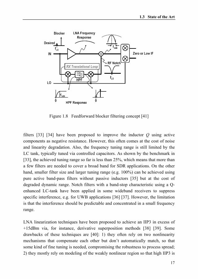
Figure 1.8 Feedforward blocker filtering concept [41] filters [33] [34] have been proposed to improve the inductor Q using active components as negative resistance. However, this often comes at the cost of noise and linearity degradation. Also, the frequency tuning range is still limited by the LC tank, typically tuned via controlled capacitors. As shown by the benchmark in [33], the achieved tuning range so far is less than 25%, which means that more than a few filters are needed to cover a broad band for SDR applications. On the other hand, smaller filter size and larger tuning range (e.g. 100%) can be achieved using pure active band-pass filters without passive inductors [35] but at the cost of degraded dynamic range. Notch filters with a band-stop characteristic using a Q-enhanced LC-tank have been applied in some wideband receivers to suppress specific interference, e.g. for UWB applications [36] [37]. However, the limitation is that the interference should be predictable and concentrated in a small frequency range. LNA linearization techniques have been proposed to achieve an IIP3 in excess of +15dBm via, for instance, derivative superposition methods [38] [39]. Some drawbacks of these techniques are [40]: 1) they often rely on two nonlinearity mechanisms that compensate each other but don’t automatically match, so that some kind of fine tuning is needed, compromising the robustness to process spread; 2) they mostly rely on modeling of the weakly nonlinear region so that high IIP3 is

Chapter 1 Introduction
18
only achieved for low input interference power while there is only limited or even no benefit for strong interference. Recently, a flexible blocker filtering technique has been presented to cancel blockers at the output of the LNA [41], as shown in Fig. 1.8. Blocker reduction is achieved by means of an auxiliary feedforward path, using two mixers with a high-pass filter (HPF) in between. This auxiliary path conducts the undesired interferers and suppresses them by subtracting them from the main signal path at the output of the LNA. However, it comes at significant cost in terms of noise and power consumption due to the additional feedforward signal path and its performance relies on the matching between the main path and the auxiliary path. We will see later in Chapter 5 that an equivalent functionality can be achieved with much simpler hardware.
b) Harmonic Mixing
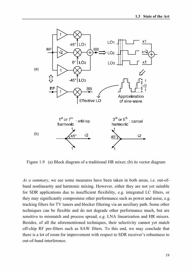
Harmonic-rejection (HR) mixers using multi-phase square-wave LOs driving parallel operating mixers have been proposed [42]. Fig. 1.9 (a) shows an example, where the weighted current outputs add up to approximate mixing with a sine-wave LO. All even-order harmonics can be suppressed by a balanced LO. The combination of an amplitude ratio of 1:√2:1 and an 8-phase LO (equidistant 45°) can reject the 3rd and 5th harmonics, as shown in the vector diagram of Fig. 1.9 (b). The 7th harmonic is not rejected and still needs to be removed by filtering, but the filter requirement is strongly relaxed compared to the case of a normal double-balanced I/Q mixer whose first un-rejected harmonic is the 3rd order. However, the achievable HR ratio is typically limited to 30-to-40dB [23] [43] [44] by the accuracy of the LO phases and the amplitude ratios, e.g. the irrational amplitude ratio of 1:√2:1. To improve the limited HR ratio in a mixer, the state-of-the-art wideband TV tuners rely on RF-tracking filters together with HR mixers [43] [44] to guarantee more than 65dB HR ratio. However, these tracking filters cost power, take area, and introduce extra noise and distortion. For example, the 4th-order band-pass Gm-C tracking filter in [43] achieves a 7dB gain, a 17dB NF, and a +7dBm IIP3 while consuming 72mW power.
1.3 State of the Art
19
Figure 1.9 (a) Block diagram of a traditional HR mixer; (b) its vector diagram As a summary, we see some measures have been taken in both areas, i.e. out-of-band nonlinearity and harmonic mixing. However, either they are not yet suitable for SDR applications due to insufficient flexibility, e.g. integrated LC filters, or they may significantly compromise other performance such as power and noise, e.g. tracking filters for TV tuners and blocker filtering via an auxiliary path. Some other techniques can be flexible and do not degrade other performance much, but are sensitive to mismatch and process spread, e.g. LNA linearization and HR mixers. Besides, of all the aforementioned techniques, their selectivity cannot yet match off-chip RF pre-filters such as SAW filters. To this end, we may conclude that there is a lot of room for improvement with respect to SDR receiver’s robustness to out-of-band interference.
Chapter 1 Introduction
20
1.3.3 Flexible Baseband Channel Selection
Generally for the baseband-filter design, there exists a trade-off between bandwidth, noise, and filter order versus power consumption. Two classes of filters have been proposed for flexible SDR receivers: continuous-time (CT) and discrete-time (DT) filters. Both have shown promising results. The IMEC SDR transceiver [24] applies CT baseband filters constructed via a cascade of two active-Gm-RC biquads and a Rauch biquad. It may continuously cover a bandwidth of 0.35MHz to 23.5MHz with a programmable 2nd, 4th or 6th order. It can achieve a 12-bit frequency-tuning resolution via a combination of a 5-bit coarse tuning using a resistor array and a 7-bit fine tuning using a capacitor array [45]. Their second-generation SDR receiver also employs CT baseband filtering [26]. Flexible baseband DT filters have also been developed. The UCLA SDR receiver [23] uses a passive switched–capacitor filter demonstrated for the GSM and the 802.11g standards, tunable via changing sampling rate and decimation ratios. However, continuous frequency tunability was not shown. The active-Gm switched-capacitor filter from NEC [46] can cover 0.4MHz to 30MHz continuously tunable via a DT transconductor controlled by clock duty cycle, with a 2nd or 4th order characteristic. The frequency-tuning resolution was not mentioned but depends on the resolution of the clock duty cycle. The baseband filter in the Bitwave “Softransceiver” [27] can continuously cover the bandwidth of 25kHz to 20MHz in more than 1000 steps and can support all major cellular, WLAN, and broadcast standards. It is unclear whether the filter is in CT or DT implementation. From the above examples, we can see that many promising solutions have been demonstrated for the flexible baseband filtering and basically can satisfy the SDR applications. Especially, some have been built into products such as [27].

1.4 Research Objectives
21
1.3.4 Compatibility with CMOS Scaling and SoC Integration
As shown in Section 1.3.1, using new design techniques, many wideband radio receivers have been demonstrated in advanced CMOS technology, e.g. 90nm [23], 65nm [30], and 45nm [26]. However, it is another degree of challenge to integrate radio transceivers and digital (de)modulators on the same chip, due to, e.g. digital switching noise. Direct RF-sampling receivers seem to be a good candidate, both for better compatibility with CMOS scaling [47]-[49] and SoC integration [50] [51]. They sample the signal early in the receiver chain before or simultaneously with downconversion, instead of after downconversion which is done in RF-mixing receivers. A few RF-sampling receivers for commercial products have been presented [48]-[51], including what is claimed to be the first published [51] commercial SoC for quad-band GSM in 90nm baseline digital CMOS with no analog extension. However, all of these RF-sampling receivers are dedicated to one narrowband standard and all the aforementioned wideband receivers in Section 1.3.1 are based on RF mixing. Further research is needed to evaluate the suitability of RF sampling for SDR applications, and we will address this subject in Chapter 2. Till this point, we have discussed the challenges of realizing a SDR receiver and some state-of-the-art solutions in literature. The next section will discuss our research objectives and the challenges we are going to address, while also clarifying the added value to other work.
1.4 Research Objectives After summarizing the previous section, we may conclude that lots of solutions have been proposed for wideband receivers and flexible baseband filtering, showing promising results. However, the other two challenges, of handling OBI in a wideband receiver and of realizing a SDR in a downscaled CMOS with SoC integration, still have a long way to go.

Chapter 1 Introduction
22
This thesis aims at finding: 1) techniques to improve the robustness of wideband receivers to OBI; 2) techniques for wideband receivers compatible with CMOS scaling and SoC integration. To address the challenge due to OBI, we should look at both mechanisms: out-of-band nonlinearity and harmonic mixing. After amplification by an LNA, the burden of the nonlinearity is mainly on the mixer while harmonic mixing also happens in the mixer. Therefore, this thesis will focus on frequency translation related innovations to improve the receivers’ robustness to OBI. The work aims at removing RF pre-filters or at least drastically relaxing their requirements. As described in the previous section, RF-sampling receivers can bring two advantages: compatibility with CMOS scaling and SoC integration. However, as will be discussed in Chapter 2, current RF-sampling techniques do not directly fit wideband SDR applications. To our knowledge, all the wideband receivers shown by other researchers so far are based on RF mixing but not RF sampling. We will explore new RF-sampling techniques more suitable for wideband SDR receivers, which also involve new frequency translation techniques. The title of the thesis refers to the above mentioned goals. This thesis mainly explores “frequency translation techniques” to improve the “interference-robust” characteristic of “software-defined radio receivers” and to make them compatible with CMOS scaling and SoC integration. Moreover, the thesis also describes some filter and amplifier techniques which support interference-robustness. Based on the foregoing discussions, now we set our concrete research objectives:
Develop new RF-sampling receivers for wideband applications Enhance the out-of-band linearity of wideband receivers Improve the robustness of harmonic rejection to mismatch
1.5 Thesis Organization The rest of the thesis is organized as follows:
1.5 Thesis Organization
23
Chapter 2 discusses fundamental differences of frequency translation (FT) techniques for radio receivers, via a classification and comparison for FT techniques based on mixing and sampling principles [52]. This also leads to the definition of a discrete-time (DT) mixing technique. Moreover, we will evaluate the suitability of RF-mixing and RF-sampling receivers to SDR and analyze the challenges of applying RF sampling to wideband receivers [53]. Chapter 3 elaborates the DT mixing technique [52] [54], which can make RF sampling more suitable to SDR receivers by achieving two wideband features: wideband quadrature demodulation and wideband harmonic rejection. To verify the concept, a 200-to-900MHz DT-mixing downconverter with 8-times oversampling and 2nd-to-6th HR is implemented in 65nm CMOS. Chapter 4 describes a tunable LC filter and a linearized LNA [55] [56], applied as pre-stages of the DT-mixing downconverter to construct a complete RF-sampling receiver achieving a minimum NF as low as 0.8dB. To make the receiver more robust to interference, the tunable LC filter improves the HR ratio flexibly and the LNA exploits a new linearity enhancement technique. Furthermore, Chapter 5 proposes two frequency translation techniques for an interference-robust SDR receiver [57] [58], one to improve the out-of-band linearity and the other to make the HR robust to mismatch. To demonstrate these two concepts, a 65nm CMOS receiver based on RF mixing shows that +3.5dBm in-band IIP3 and +16dBm out-of-band IIP3 can be achieved. More than 60dB HR ratio is measured over 40 randomly-selected chips while more than 80dB becomes possible with digitally-enhanced HR. The proposed accurate multi-phase LO generator works up to 0.9GHz while the RF bandwidth is measured up to 6GHz. Chapter 6 draws conclusions, summarizes the main contributions of this work, and suggests some future research directions. The appendix contains two important analyses. Appendix A derives the wideband transfer function of baseband impedance to RF through mixer switches (Chapter 5), namely “mix-impedance”. Appendix B performs a statistical analysis for HR considering random amplitude and phase errors, to quantify the required accuracy to achieve a certain HR ratio (Chapter 5).
Chapter 1 Introduction
24
1.6 References [1] C. Taylor, "Global mobile penetration to reach 75% by 2011", [Online],
Available: http://www.theregister.co.uk/2007/10/26/mobile_pentration_research/
[2] J. Mitola, "Software radios-survey, critical evaluation and future directions," National Telesystems Conference, (NTC), pp.13/15-13/23, May 1992
[3] J. Mitola, "Software radios: Survey, critical evaluation and future directions," IEEE Aerospace and Electronic Systems Magazine, vol.8, no.4, pp.25-36, Apr. 1993
[4] J. Mitola, "The software radio architecture," IEEE Communications Magazine, vol.33, no.5, pp.26-38, May 1995
[5] J. Mitola, "Software radio architecture: a mathematical perspective," IEEE J. Selected Areas in Communications, vol.17, no.4, pp.514-538, Apr. 1999
[6] E.A.M. Klumperink, R. Shrestha, E. Mensink, V.J. Arkesteijn, B. Nauta, "Cognitive radios for dynamic spectrum access - polyphase multipath radio circuits for dynamic spectrum access," IEEE Communications Magazine, vol.45, no.5, pp.104-112, May 2007
[7] The Software Defined Radio Request for Information. Atlanta, GA: BellSouth, Dec. 1995
[8] J. Mitola, G.Q. Maguire, "Cognitive radio: making software radios more personal," IEEE Personal Communications, vol.6, no.4, pp.13-18, Aug. 1999
[9] The Federal Communications Commission (FCC), “Notice for Proposed Rulemaking (NPRM 03 322): Facilitating Opportunities for Flexible, efficient, and Reliable Spectrum Use Employing Spectrum agile Radio Technologies”, ET Docket No. 03 108, Dec. 2003
[10] A.-J. Annema, B. Nauta, R. van Langevelde, H. Tuinhout, "Analog circuits in ultra-deep-submicron CMOS," IEEE J. Solid-State Circuits, vol.40, no.1, pp. 132-143, Jan. 2005
[11] GSM Technical Specification 05.05, European Telecommunications Standards Institute, Sophia Antipolis, France, 1992
[12] M. Brandolini, P. Rossi, D. Manstretta, F. Svelto, "Toward multistandard mobile terminals - fully integrated receivers requirements and architectures," IEEE Trans. Microwave Theory and Techniques, vol.53, no.3, pp. 1026-1038, Mar. 2005

1.6 References
25
[13] D. Manstretta, N. Laurenti and R. Castello, "A Reconfigurable Narrow-Band MB-OFDM UWB Receiver Architecture," IEEE Trans. Circuits and Systems II: Express Briefs, vol.55, no.4, pp.324-328, Apr. 2008
[14] C.T.-C. Nguyen, "Vibrating RF MEMS for next generation wireless applications," IEEE CICC, Proc., pp. 257-264, Oct. 2004
[15] B. Razavi, “RF Microelectronics”, Prentice Hall, Upper Saddle River, NJ, 1998
[16] R. Pullela, S. Tadjpour, D. Rozenblit, et. al. "An integrated closed-loop polar transmitter with saturation prevention and low-IF receiver for quad-band GPRS/EDGE," IEEE ISSCC, Dig. Tech. Papers, pp.112-113,113a, Feb. 2009
[17] F. Bruccoleri, E.A.M. Klumperink, B. Nauta, "Wide-band CMOS low-noise amplifier exploiting thermal noise canceling," IEEE J. Solid-State Circuits, vol.39, no.2, pp. 275-282, Feb. 2004
[18] C.-F. Liao, S.-I. Liu, "A Broadband Noise-Canceling CMOS LNA for 3.1–10.6-GHz UWB Receivers," IEEE J. Solid-State Circuits, vol.42, no.2, pp.329-339, Feb. 2007
[19] J.-H.C. Zhan, S.S. Taylor, "A 5GHz resistive-feedback CMOS LNA for low-cost multi-standard applications," IEEE ISSCC, Dig. Tech. Papers, pp.721-730, Feb. 2006
[20] J. Borremans, P. Wambacq, C. Soens, Y. Rolain, M. Kuijk, "Low-Area Active-Feedback Low-Noise Amplifier Design in Scaled Digital CMOS," IEEE J. Solid-State Circuits, vol.43, no.11, pp.2422-2433, Nov. 2008
[21] H.S. Bennett, R. Brederlow, J.C. Costa, P.E. Cottrell, W.M. Huang, A.A. Immorlica, et. al., "Device and technology evolution for Si-based RF integrated circuits," IEEE Trans. Electron Devices, vol.52, no.7, pp. 1235-1258, July 2005
[22] V.J. Arkesteijn, E.A.M. Klumperink, B. Nauta, "A wideband high-linearity RF receiver front-end in CMOS," ESSCIRC, Proc., pp. 71-74, Sept. 2004
[23] R. Bagheri, A. Mirzaei, S. Chehrazi, et. al. "An 800MHz to 5GHz Software-Defined Radio Receiver in 90nm CMOS," IEEE ISSCC, Dig. Tech. Papers, pp.1932-1941, Feb. 2006
[24] J. Craninckx, M. Liu, D. Hauspie, et. al., "A Fully Reconfigurable Software-Defined Radio Transceiver in 0.13μm CMOS," IEEE ISSCC, Dig. Tech. Papers, pp.346-607, Feb. 2007

Chapter 1 Introduction
26
[25] M. Ingels, C. Soens, J. Craninckx, et. al., "A CMOS 100MHz to 6GHz software defined radio analog front-end with integrated pre-power amplifier," ESSCIRC, Proc., pp.436-439, Sept. 2007
[26] V. Giannini, P. Nuzzo, C. Soens, et. al., "A 2mm2 0.1-to-5GHz SDR receiver in 45nm digital CMOS," IEEE ISSCC, Dig. Tech. Papers, pp.408-409, Feb. 2009
[27] BitWave Semiconductor, The BW1102 Softransceiver Product Brief, [Online], Available: http://www.bitwavesemiconductor.com/pdf/ 1014BWS06SLS-G-SoftransceiverProductBrief.pdf
[28] R. van de Beek, J. Bergervoet, H. Kundur, et. al., "A 0.6-to-10GHz Receiver Front-End in 45nm CMOS," IEEE ISSCC, Dig. Tech. Papers, pp.128-601, Feb. 2008
[29] D. Leenaerts, R. van de Beek, J. Bergervoet, et. al., "A 65nm CMOS inductorless triple-band-group WiMedia UWB PHY," IEEE ISSCC, Dig. Tech. Papers, pp.410-411,411a, Feb. 2009
[30] S. Blaakmeer, E.A.M. Klumperink, D, Leenaerts, B. Nauta, "A Wideband Balun LNA I/Q-Mixer combination in 65nm CMOS," IEEE ISSCC, Dig. Tech. Papers, pp.326-617, Feb. 2008
[31] B. Razavi, “Design of Analog CMOS Integrated Circuits”, McGraw-Hill, 2000
[32] V. Arkesteijn, “Analog front-ends for software-defined radio receivers”, Ph.D. Dissertation, University of Twente, Netherlands, 2007
[33] B. Georgescu, I.G. Finvers, F. Ghannouchi, "2GHz Q-Enhanced Active Filter With Low Passband Distortion and High Dynamic Range," IEEE J. Solid-State Circuits, vol.41, no.9, pp.2029-2039, Sept. 2006
[34] X. He, W.B. Kuhn, "A 2.5-GHz low-power, high dynamic range, self-tuned Q-enhanced LC filter in SOI," IEEE J. Solid-State Circuits, vol.40, no.8, pp. 1618-1628, Aug. 2005
[35] Y. Wu, X. Ding, M. Ismail, H. Olsson, "RF bandpass filter design based on CMOS active inductors," IEEE Trans. Circuits and Systems II: Analog and Digital Signal Processing, vol.50, no.12, pp. 942-949, Dec. 2003
[36] A. Valdes-Garcia, C. Mishra, F. Bahmani, J. Silva-Martinez, E. Sanchez-Sinencio, "An 11-Band 3–10 GHz Receiver in SiGe BiCMOS for Multiband OFDM UWB Communication," IEEE J. Solid-State Circuits, vol.42, no.4, pp.935-948, Apr. 2007

1.6 References
27
[37] A. Vallese, A. Bevilacqua, C. Sandner, M. Tiebout, A. Gerosa, A. Neviani, "Analysis and Design of an Integrated Notch Filter for the Rejection of Interference in UWB Systems," IEEE J. Solid-State Circuits, vol.44, no.2, pp.331-343, Feb. 2009
[38] V. Aparin, L.E. Larson, "Modified derivative superposition method for linearizing FET low-noise amplifiers," IEEE Trans. Microwave Theory and Techniques, vol.53, no.2, pp.571-581, Feb. 2005
[39] W.-H. Chen, G. Liu, B. Zdravko, A.M. Niknejad, "A Highly Linear Broadband CMOS LNA Employing Noise and Distortion Cancellation," IEEE J. Solid-State Circuits, vol.43, no.5, pp.1164-1176, May 2008
[40] E.A.M. Klumperink, B. Nauta, "Systematic comparison of HF CMOS transconductors," IEEE Trans. Circuits and Systems II: Analog and Digital Signal Processing, vol.50, no.10, pp. 728-741, Oct. 2003
[41] H. Darabi, "A Blocker Filtering Technique for SAW-less Wireless Receivers," IEEE J. Solid-State Circuits, vol.42, no.12, pp.2766-2773, Dec. 2007
[42] J.A. Weldon, R.S. Narayanaswami, J.C. Rudell, et. al., "A 1.75-GHz highly integrated narrow-band CMOS transmitter with harmonic-rejection mixers," IEEE J. Solid-State Circuits, vol.36, no.12, pp.2003-2015, Dec. 2001
[43] S. Lerstaveesin, M. Gupta, D. Kang, B.-S. Song, "A 48–860 MHz CMOS Low-IF Direct-Conversion DTV Tuner," IEEE J. Solid-State Circuits, vol.43, no.9, pp.2013-2024, Sept. 2008
[44] F. Gatta, R. Gomez, Y. Shin, et al., “An Embedded 65nm CMOS Low-IF 48MHz-to-1GHz Dual Tuner for DOCSIS 3.0”, IEEE ISSCC, Dig. Tech. Papers, pp.122-123, Feb. 2009
[45] V. Giannini, J. Craninckx, S. D'Amico, A. Baschirotto, "Flexible Baseband Analog Circuits for Software-Defined Radio Front-Ends," IEEE J. Solid-State Circuits, vol.42, no.7, pp.1501-1512, July 2007
[46] M. Kitsunezuka, S. Hori, T. Maeda, "A Widely-Tunable Reconfigurable CMOS Analog Baseband IC for Software-Defined Radio," IEEE ISSCC, Dig. Tech. Papers, pp.66-595, Feb. 2008
[47] K. Muhammad, R.B. Staszewski, "Direct RF sampling mixer with recursive filtering in charge domain," IEEE ISCAS, Proc, pp. I-577-80 Vol.1, May 2004
[48] R.B. Staszewski, K. Muhammad, D. Leipold, et. al., "All-digital TX frequency synthesizer and discrete-time receiver for Bluetooth radio in 130-nm CMOS," IEEE J. Solid-State Circuits, vol.39, no.12, pp. 2278-2291, Dec. 2004

Chapter 1 Introduction
28
[49] F. Montaudon, R. Mina, S. Le Tual, et. al., "A Scalable 2.4-to-2.7GHz Wi-Fi/ WiMAX Discrete-Time Receiver in 65nm CMOS," IEEE ISSCC, Dig. Tech. Papers, pp.362-619, 3-7 Feb. 2008
[50] K. Muhammad, H. Yo-Chuol, T.L. Mayhugh, et. al., "The First Fully Integrated Quad-Band GSM/GPRS Receiver in a 90-nm Digital CMOS Process," IEEE J. Solid-State Circuits, vol.41, no.8, pp.1772-1783, Aug. 2006
[51] R.B. Staszewski, D. Leipold, O. Eliezer, et. al., "A 24mm2 Quad-Band Single-Chip GSM Radio with Transmitter Calibration in 90nm Digital CMOS," IEEE ISSCC, Dig. Tech. Papers, pp.208-607, Feb. 2008
[52] Z. Ru, E.A.M. Klumperink, B. Nauta, “Discrete-Time Mixing Receiver Architecture for RF-Sampling Software-Defined Radio”, submitted to IEEE J. Solid-State Circuits
[53] Z. Ru, E.A.M. Klumperink, B. Nauta, "On the Suitability of Discrete-Time Receivers for Software-Defined Radio," IEEE ISCAS, pp.2522-2525, May 2007
[54] Z. Ru, E.A.M. Klumperink, B. Nauta, "A Discrete-Time Mixing Receiver Architecture with Wideband Harmonic Rejection", IEEE ISSCC, Dig. Tech. Papers, pp.322-323., Feb. 2008
[55] Z. Ru, E.A.M. Klumperink, C.E. Saavedra, B. Nauta, "A tunable 300–800MHz RF-sampling receiver achieving 60dB harmonic rejection and 0.8dB minimum NF in 65nm CMOS," IEEE RFIC Symposium, pp.21-24, June 2009
[56] Z. Ru, E.A.M. Klumperink, C.E. Saavedra, B. Nauta, "A 300-800MHz Tunable Filter and Linearized LNA applied in a Low-Noise Harmonic-Rejection RF-Sampling Receiver", submitted to IEEE J. Solid-State Circuits, Special Issue on RFIC Symposium 2009
[57] Z. Ru, E.A.M. Klumperink, G.J.M. Wienk, B. Nauta, "A software-defined radio receiver architecture robust to out-of-band interference," IEEE ISSCC, Dig. Tech. Papers, pp.230-231, Feb. 2009
[58] Z. Ru, N.A. Moseley, E.A.M. Klumperink, B. Nauta, “Digitally-Enhanced Software-Defined Radio Receiver Robust to Out-of-Band Interference”, accepted by IEEE J. Solid-State Circuits, Dec. 2009

29
Chapter 2 Frequency Translation Fundamentals From Section 1.4, we know that frequency translation (FT) techniques will be a focus of this thesis. This chapter discusses fundamental differences among various FT techniques for radio receivers, with an emphasis on downconversion. It serves as a theoretical base for the follow-up chapters (Chapter 3 to 5) which will present circuits and systems around various types of FT techniques. Chapter 2 starts with a brief introduction on the main reasons for applying FT in radios in Section 2.1. To clarify different downconversion techniques, in Section 2.2 we present a classification of them [1]. This also leads to the definition of a discrete-time (DT) mixing technique which is the subject of the next two chapters. To further clarify the classification criteria, Section 2.3 compares mixing and sampling principles, stressing on their fundamental distinctions. Based on the classification, Section 2.4 comes up with three receiver architectures and discusses their suitability to SDR applications. Among these architectures, RF-sampling receivers show some advantages on the compatibility with CMOS scaling and SoC integration. However, traditional RF-sampling techniques also present some drawbacks for wideband SDR applications. Therefore, in Section 2.5, we analyze the challenges of applying RF sampling to wideband receivers [2]. These challenges can be solved via techniques presented in the next chapter. Chapter 2 ends with conclusions (Section 2.6) and references (Section 2.7).
Chapter 2 Frequency Translation Fundamentals
30
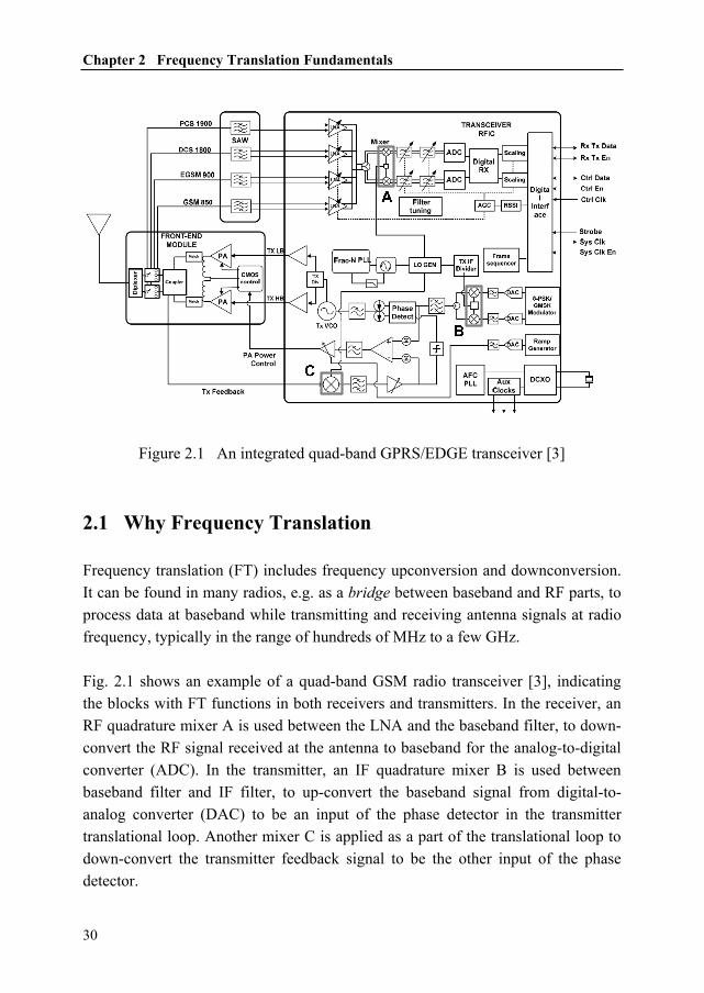
Figure 2.1 An integrated quad-band GPRS/EDGE transceiver [3]
2.1 Why Frequency Translation Frequency translation (FT) includes frequency upconversion and downconversion. It can be found in many radios, e.g. as a bridge between baseband and RF parts, to process data at baseband while transmitting and receiving antenna signals at radio frequency, typically in the range of hundreds of MHz to a few GHz. Fig. 2.1 shows an example of a quad-band GSM radio transceiver [3], indicating the blocks with FT functions in both receivers and transmitters. In the receiver, an RF quadrature mixer A is used between the LNA and the baseband filter, to down-convert the RF signal received at the antenna to baseband for the analog-to-digital converter (ADC). In the transmitter, an IF quadrature mixer B is used between baseband filter and IF filter, to up-convert the baseband signal from digital-to-analog converter (DAC) to be an input of the phase detector in the transmitter translational loop. Another mixer C is applied as a part of the translational loop to down-convert the transmitter feedback signal to be the other input of the phase detector.

2.1 Why Frequency Translation
31
Figure 2.2 Block diagram of a typical radio receiver indicating AFE There are two main reasons why we want FT in a radio: feasibility and power consumption. To explain this further, we first look at the receiver side. In fact, a major function of an analog front-end (Fig. 2.2) is to assist in the conversion of an antenna signal into the digital domain1 , for advanced signal processing. Simply put, the analog front-end makes the job of the ADC easier with respect to the required speed and dynamic range (DR). The down-mixer is responsible for reducing the speed, from RF to baseband. Two other important blocks are the channel-selection filter (CSF), which suppresses interferers to reduce the required DR of an ADC, and the variable-gain amplifier (VGA), which controls the gain to reduce the DR of the desired signal and the unsuppressed interferers. Without downconversion, the ADC in a radio receiver is often unfeasible, due to a higher speed required at a high DR. For instance, a GSM receiver can require an ADC resolution as high as 14 bits [4], even with the assistance of a VGA and a channel filter. Without downconversion, reception of a GSM signal at 1.9GHz asks for a 14-bit ADC running at a speed of at least 3.8GS/s (Nyquist rate). However, the reported state-of-the-art CMOS ADCs can only achieve 34dB (5.5-bit) signal-to-noise-and-distortion ratio (SNDR) at 2.5GS/s with 1.1GHz bandwidth [5] or 56dB (9-bit) SNDR at 1GS/s with 500MHz bandwidth [6]. An overview of the top ADCs published in recent years can be found in [7] but none is even close to the desired performance of about 4GS/s and 14 bits.
1 Otherwise pure analog demodulation is also possible.

Chapter 2 Frequency Translation Fundamentals
32
Please note that the actual required ADC resolution, without downconversoin ahead, is likely to be higher than what is typically required today for an ADC after downconversion. A key reason is that a band-pass (BP) channel-selection filter used in case of no downconversion is more challenging to make than a low-pass (LP) one. In the end, such a BP channel filter may be even not feasible or achieved with lower order and Q-factor. This can require a higher-resolution ADC due to a higher DR caused by stronger in-band interference since the BP channel selection is less effective. Moreover, if including out-of-band interference into consideration, e.g. for SDR applications, the requirement on the ADC will be even more stringent. One step back. Even if such an ADC (and BP channel filter) can be feasible in the future, the power consumption of the whole radio is likely to be unnecessarily high. Without downconversion, it is not just the ADC to run at RF speed, e.g. in the GHz range, but also the channel filter, the VGA, and the digital front-end. However, the desired signal protocol (channel) bandwidth is often on the order of 1000 times smaller, e.g. in the MHz range. A lower operating speed means a lower overall power consumption, both for active analog circuits such as amplifiers and filters (static power) and for switching circuits such as quantizers and digital gates (dynamic power). Without downconversion early in the receiver chain, the required power of the whole radio would be dramatically increased. For mobile applications, the reduced power consumption is a key advantage of applying downconversion early in a receiver, although the resulted architecture might not be as flexible as the ideal software-radio receiver (see Section 1.1). Other than in receivers, frequency translation blocks are also widely applied in transmitters (Fig. 2.1), for either downconversion or upconversion. They usually share a similar motivation as for receivers, i.e. to make functions such as AD/DA conversion and phase detection feasible and to reduce the power consumption of the entire system. This thesis mainly focuses on the receiver side, mostly involving frequency downconversion which is also the main subject of the rest of this chapter. Nevertheless, upconversion can be regarded as a counterpart, sharing most of the discussed principles.

2.2 Classification of Downconversion Techniques
33
InputPrinciple
Analog-CT(CT CA)
Analog-DT(DT CA)
Digital(DT DA)
Mixing CT Mixing1 DT Mixing2
(proposed)Digital Mixing3
Sampling CT-to-DT Sampling2
DT Re-sampling2
Digital Re-sampling3
InputPrinciple
Analog-CT(CT CA)
Analog-DT(DT CA)
Digital(DT DA)
Mixing CT Mixing1 DT Mixing2
(proposed)Digital Mixing3
Sampling CT-to-DT Sampling2
DT Re-sampling2
Digital Re-sampling3
2RF-sampling receiver1RF-mixing receiver 3Ideal SWR receiver Table 2.1 Classification of frequency downconversion techniques based on
the type of input signal and the downconversion principle Different frequency downconversion techniques have been proposed for radio receivers, most notably mixing and sampling. We would like to compare them and answer questions such as: what are the fundamental distinctions among them, is it really more flexible to sample as early as possible in a receiver chain, and does sampling suffer more from clock jitter compared to mixing? In order to clarify the differences among downconversion techniques, we first propose a classification of them.
2.2 Classification of Downconversion Techniques Table 2.1 classifies various downconversion techniques based on two aspects. The columns are defined by the input signal domain, i.e. continuous-time (CT) versus discrete-time and continuous-amplitude versus discrete-amplitude 2 . The rows distinguish in downconversion principle, i.e. mixing or sampling3.
2 A column for continuous-time discrete-amplitude signal can also be added, but we omitted it because we are not aware of any practical radio examples yet operating in this domain, although some work [8] [9] tried to explore the potential benefits of CT DSP systems. Such type of signal often appears at the output of a digital-to-analog converter before applying a reconstruction filter. 3 Please note that sampling always provides a DT output, and hence it provides CT to DT conversion in case of a CT input, while under certain conditions as will be described in Section 2.3.2, it can also provide frequency translation.
Chapter 2 Frequency Translation Fundamentals
34
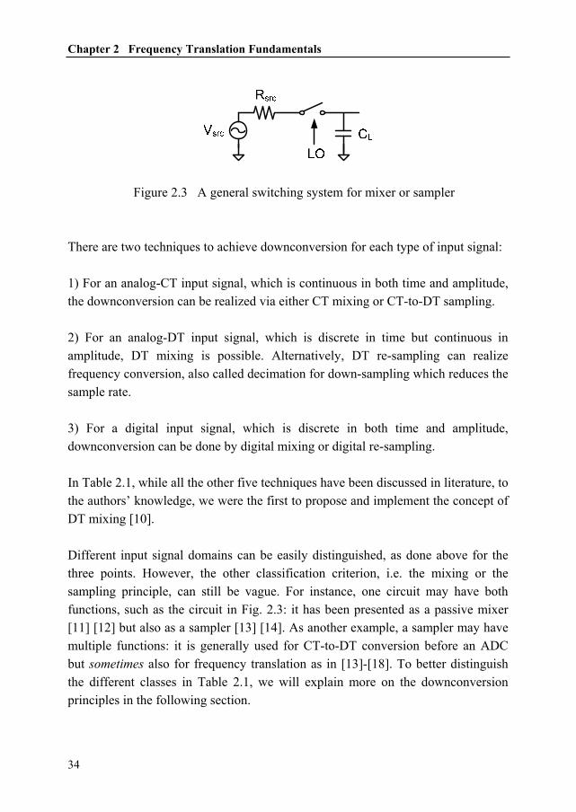
Figure 2.3 A general switching system for mixer or sampler
There are two techniques to achieve downconversion for each type of input signal: 1) For an analog-CT input signal, which is continuous in both time and amplitude, the downconversion can be realized via either CT mixing or CT-to-DT sampling. 2) For an analog-DT input signal, which is discrete in time but continuous in amplitude, DT mixing is possible. Alternatively, DT re-sampling can realize frequency conversion, also called decimation for down-sampling which reduces the sample rate. 3) For a digital input signal, which is discrete in both time and amplitude, downconversion can be done by digital mixing or digital re-sampling. In Table 2.1, while all the other five techniques have been discussed in literature, to the authors’ knowledge, we were the first to propose and implement the concept of DT mixing [10]. Different input signal domains can be easily distinguished, as done above for the three points. However, the other classification criterion, i.e. the mixing or the sampling principle, can still be vague. For instance, one circuit may have both functions, such as the circuit in Fig. 2.3: it has been presented as a passive mixer [11] [12] but also as a sampler [13] [14]. As another example, a sampler may have multiple functions: it is generally used for CT-to-DT conversion before an ADC but sometimes also for frequency translation as in [13]-[18]. To better distinguish the different classes in Table 2.1, we will explain more on the downconversion principles in the following section.
2.3 Fundamental Distinctions between Mixing and Sampling Principles
35
2.3 Fundamental Distinctions between Mixing and Sampling Principles
We will now try to find fundamental distinctions between the mixing and the sampling principles, from both a time-domain and a frequency-domain point of view.
2.3.1 Time Domain: Information Rate Changes or Not?
It is well known that mixing can be modeled as a multiplication in the time domain, while sampling can also be described via multiplication. For instance, CT-to-DT sampling can be modeled as multiplying a CT input signal x(t) with a Dirac comb δT(t)=Σδ(t-n·TLO), n=-∞…+∞, and the sampled signal xs(t) is then:
( ) ( ) ( )1 1( ) ( ) ( ) ( )
Fourier
s T
s LO LOn nLO LO
x t x t t
X f X f f nf X f nfT T
δ
δ+∞ +∞
=−∞ =−∞
= ⋅ ↔
= ⊗ − = −∑ ∑. (2.1)
X(f) and Xs(f) are Fourier transforms of x(t) and xs(t) respectively. Equation (2.1) is commonly used to describe ideal sampling; however, the scaling factor 1/TLO is often neglected. On might wonder whether this means that the “gain” of sampling is 1/TLO, with a unit of “Hz”. Analysis leads to the conclusion that this is not the case. In fact, sampling is more than just multiplication. There is an important step after (2.1), i.e. CT-to-DT conversion. The signals x(t), δT(t), and xs(t) are all defined in the CT domain. If we convert xs(t) into the DT domain as xs(k) and apply DT Fourier transform, we will get a frequency-domain (FD) representation with continuous but normalized frequency axis, i.e. f/fLO. Such a ratio can be defined as “r”: r=f/fLO. We can also obtain the r-axis FD representation by substituting f=r·fLO into (2.1):
1( ) ( ) ( ) ( ) ( )s LO LO LO LO LOn nLO
X r f X r f r f nf X r f r nT
δ δ+∞ +∞
=−∞ =−∞
⋅ = ⋅ ⊗ ⋅ − = ⋅ ⊗ −∑ ∑ . (2.2)
Note that the factor 1/TLO goes away in (2.2), due to the scaling property of δ-function. If we define Ys(r)=Xs(r·fLO) and Y(r)=X(r·fLO), then (2.2) can be written as
( ) ( ) ( ) ( )sn n
Y r Y r r n Y r nδ+∞ +∞
=−∞ =−∞
= ⊗ − = −∑ ∑ . (2.3)
Chapter 2 Frequency Translation Fundamentals
36
Ys(r) is the FD representation for xs(k). Note that “r” is a continuous real number. Comparing (2.3) to (2.1), we can see that after converting the sampled signal xs(t) into the DT domain, the scaling factor 1/TLO disappears and the gain of ideal sampling is 1, as normally expected. Therefore the step of CT-to-DT conversion is vital for a sampling operation. We might look at this step as a way to reduce the information rate from infinite (CT information) to finite (DT data). Thus CT-to-DT sampling nicely fits in one row with DT re-sampling or digital re-sampling, all in the second row of Table 2.1, sharing the property of decreased information rate, i.e. decimation for downconversion. In contrast, all the mixing techniques do not change the information rate from input to output, neither for CT mixing and DT mixing nor for digital mixing. This time-domain property can serve as an important distinction between mixing and sampling. For example, although a CT mixer and a CT-to-DT sampler have a similar implementation as shown in Fig. 2.3, there is a simple distinction between them: how the output signal is used. If the output signal is used as CT information, i.e. CT signal processing follows, then it is a CT mixer, but if it is used as DT information, i.e. DT signal processing follows, then it is a CT-to-DT sampler. Thus the distinction is not in the circuit itself but in the way of interpreting the output, i.e. whether the information rate changes from input to output or not. With this distinction in mind, we see that a CT-to-DT sampler does not present a “hold effect”4 in contrast to a sample-and-hold (S/H) with a CT output. Therefore, in this thesis, we will use the letter “S” in the symbol for sampler but not “S/H”, as shown later in figures.
2.3.2 Frequency Domain: Frequency Translation Happens or Not?
Another distinction between mixing and sampling is visible in the frequency 4 On the other hand, a “hold effect” can provide DT-to-CT conversion, e.g. following a digital-to-analog converter. Effectively a hold can increase information rate from finite (DT) to infinite (CT), like interpolation. In fact, applying a “hold effect” introduces a coefficient proportional to the holding time, and the factor of 1/TLO in (2.1) can be cancelled. Therefore we can view (2.1) as an intermediate step, and the next step can be either CT-to-DT conversion (CT-to-DT sampler) or a hold (sample-and-hold).

2.3 Fundamental Distinctions between Mixing and Sampling Principles
37
domain. Simply put: mixing always does frequency translation while sampling may or may not. The main purpose of a mixer is mixing, i.e. “frequency translation”, while a sampler has two possible functions: it always does “information-rate conversion” in the time domain, but sometimes it also does “frequency translation”. To be concrete, let’s first look at CT mixing and CT-to-DT sampling, and then generalize the comparison to other cases in Table 2.1. Assume the input frequency is fin, and the LO frequency is fLO for mixing and the sampling frequency is fs for sampling. Using a CT mixer, the resulted spectrum is valid up to infinity due to the output’s CT nature, and the input signal will always be translated by fLO (unless fLO=0) and its existing harmonics. If the desired signal at the output is at fIF=|fin-fLO|, for downconversion fIF<fin is required, i.e. 0<fLO<2fin. Of course, the output of a CT mixer may contain spectrum not being translated, e.g. RF feed-through. However, that is often unwanted. Otherwise the mixer can be skipped. On the other hand, using a CT-to-DT sampler, due to the output’s DT nature, the resulted spectrum is valid from DC up to fs/2, while the rest contains repetitive images. Focusing on the spectrum from DC to fs/2, there are two cases: 1) If fs<2fin, the signal frequency will be translated (aliased) from fin to fIF=|fin–n·fs| (n=1,2…), where n·fs is the closest sampling tone to fin. Such a sampler is sometimes called a sampling mixer [19], as frequency translation does happen. This case is listed in Table 2.1 as CT-to-DT sampling. 2) If fs≥2fin (Nyquist rate), the “closest sampling tone” is DC and no frequency translation happens, so the output signal remains at fin, i.e. fIF=|fin–n·fs|=fin with n=0. Such a sampler corresponds to what is often used at baseband before an ADC. However, it may also be used at RF to generate an analog-DT signal or digital signal (after quantization) as the inputs for the second and the third columns in Table 2.1. However, this case is not considered in Table 2.1 which is only aimed to classify downconversion techniques. Accordingly, DT mixing or digital mixing always results in frequency translation like CT mixing, while DT re-sampling or digital re-sampling always renders

Chapter 2 Frequency Translation Fundamentals
38
Figure 2.4 Three receiver architectures: (a) RF-mixing receiver; (b) RF-sampling receiver; (c) Ideal SWR receiver
information-rate conversion as CT-to-DT sampling. But DT or digital re-sampling sometimes may also do frequency translation, depending on the relationship between the input signal frequency and the re-sampling frequency. With a clear distinction among different downconversion techniques classified in Table 2.1, we can now conceive how to apply them to different receiver architectures and discuss the suitability of these architectures to SDR applications.
2.4 Receiver Architectures for SDR As shown in Table 2.1, by their superscripts, the six classes of downconversion techniques are grouped into three receiver types. This section will discuss these receiver architectures, as illustrated in Fig. 2.4. To avoid confusion, we first clarify two points: 1) The way to group different downconversion techniques in a receiver architecture is based on necessary but insufficient conditions. For example, it is necessary to use either digital mixing or digital re-sampling for downconversion to define an ideal software-radio (SWR) receiver, but they can also be applied into other receiver architectures in combination with other downconversion techniques.
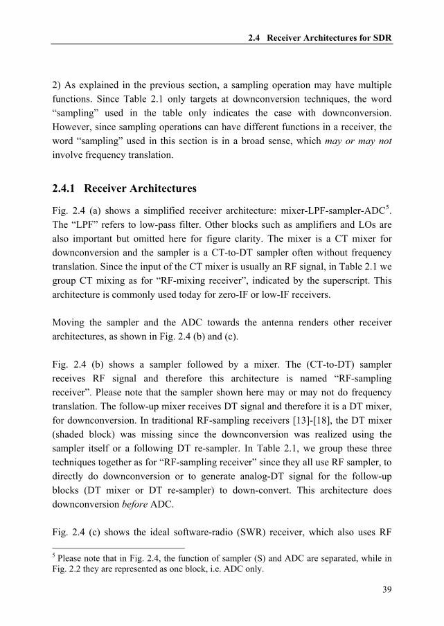
2.4 Receiver Architectures for SDR
39
2) As explained in the previous section, a sampling operation may have multiple functions. Since Table 2.1 only targets at downconversion techniques, the word “sampling” used in the table only indicates the case with downconversion. However, since sampling operations can have different functions in a receiver, the word “sampling” used in this section is in a broad sense, which may or may not involve frequency translation.
2.4.1 Receiver Architectures
Fig. 2.4 (a) shows a simplified receiver architecture: mixer-LPF-sampler-ADC5. The “LPF” refers to low-pass filter. Other blocks such as amplifiers and LOs are also important but omitted here for figure clarity. The mixer is a CT mixer for downconversion and the sampler is a CT-to-DT sampler often without frequency translation. Since the input of the CT mixer is usually an RF signal, in Table 2.1 we group CT mixing as for “RF-mixing receiver”, indicated by the superscript. This architecture is commonly used today for zero-IF or low-IF receivers. Moving the sampler and the ADC towards the antenna renders other receiver architectures, as shown in Fig. 2.4 (b) and (c). Fig. 2.4 (b) shows a sampler followed by a mixer. The (CT-to-DT) sampler receives RF signal and therefore this architecture is named “RF-sampling receiver”. Please note that the sampler shown here may or may not do frequency translation. The follow-up mixer receives DT signal and therefore it is a DT mixer, for downconversion. In traditional RF-sampling receivers [13]-[18], the DT mixer (shaded block) was missing since the downconversion was realized using the sampler itself or a following DT re-sampler. In Table 2.1, we group these three techniques together as for “RF-sampling receiver” since they all use RF sampler, to directly do downconversion or to generate analog-DT signal for the follow-up blocks (DT mixer or DT re-sampler) to down-convert. This architecture does downconversion before ADC. Fig. 2.4 (c) shows the ideal software-radio (SWR) receiver, which also uses RF 5 Please note that in Fig. 2.4, the function of sampler (S) and ADC are separated, while in Fig. 2.2 they are represented as one block, i.e. ADC only.

Chapter 2 Frequency Translation Fundamentals
40
sampler but with downconversion in the digital domain, using a digital mixer. In practice, the digital mixer can also be replaced by a digital re-sampler. In Table 2.1, we group these two items as for “ideal SWR receiver”6, which also employs RF-sampling but it does downconversion after ADC.
2.4.2 Suitability to SDR
The ideal SWR receiver may offer the maximal flexibility, as it can select and process any band or channel in the digital domain which is more flexible than analog and it can process multiple bands or channels concurrently. But for that flexibility, the ADC has to convert the full RF spectrum of interests directly into the digital domain. The RF sampler in an ideal SWR receiver does not translate desired signals in frequency, but only does so after ADC. This is different from the RF-sampling receivers implemented in [13]-[18] which still down-convert and select the desired channel in the analog domain. Therefore the main asset of an ideal SWR receiver, i.e. flexibility, is not inherently shared by the RF-sampling receivers. Although the ideal SWR receivers can be very flexible, without downconversion and filtering ahead, the required ADC performance, e.g. speed and dynamic range, is still too strict to be feasible (Section 1.1). So we will not discuss the ideal SWR receivers further in the chapter. Both the RF-mixing and the RF-sampling receivers can be suitable for SDR applications, with similarities and differences. First we look at their similarities concerning some achievable performance, such as jitter-induced error and noise figure etc.
a) Similarities
A common concern for the RF-sampling receivers is the clock jitter. It can be shown [20] that for SDR receivers the jitter induced error using the RF-mixing receivers is proportional to the LO frequency fLO, while for RF sampling it is
6 To be precise, we may call Fig. 2.4 (b) as “RF-sampling analog-downconversion receiver” while call Fig. 2.4 (c) as “RF-sampling digital-downconversion receiver”. However, for simplicity and compatibility with literature, we use the shorter names in this thesis.

2.4 Receiver Architectures for SDR
41
proportional to the input signal frequency fin. For zero-IF or low-IF receivers, fLO and fin are almost equal, and hence the difference in jitter requirement between the RF-mixing and the RF-sampling receivers is small. The feasibility of the RF-sampling receivers for practical use has been verified [15]-[18]. A serious consequence of jitter is the reciprocal mixing between the phase noise and the interference. For SDR receivers, the requirement on phase noise will be more stringent than for narrowband receivers since a selective RF pre-filter is not readily available. The actual jitter requirement depends on the interference scenario in different standards. In practice often the out-of-band interference is strong, so the frequency distance between the desired signal and the strong interference is large. If that is the case, the jitter-induced noise in the band of interest will be small [20] since the noise power induced by jitter is mainly concentrated around the strong interference due to reciprocal mixing. Comparing the RF flexibility, there is little difference between RF mixing and RF sampling. They both require wideband RF front-end on the signal path. They both rely on changing LO frequency to vary the targeted band and hence require the same LO tuning range on the clock path. Actually there is a trade-off of flexibility between the signal path and the clock path. Sub-harmonic mixing or sub-sampling may lower the LO tuning range, i.e. more flexibility on the clock path. However, selective high-Q band-pass filtering is then likely needed to counter noise and interference folding. Such filters are difficult to implement on chip and will limit the flexibility of the signal path. Another issue is the baseband flexibility, mainly the flexibility of the channel-selection filtering. For RF sampling, the baseband filtering can be implemented using DT filters such as switched-capacitor filters. For RF-mixing, the task can be done either using CT filters, such as Gm-C filters, or DT filters. As introduced in Section 1.3.3, both types of filters, i.e. CT [21] [22] and DT [4] [23], have been demonstrated for SDR applications. For gain and linearity, which is mainly determined by active circuits such as amplifiers, we don’t see a strong preference between RF sampling and RF mixing.

Chapter 2 Frequency Translation Fundamentals
42
For noise, both approaches proved good NF in narrowband receivers. For GSM receivers, as an example, [17] based on RF sampling achieved an NF of 1.9dB and [24] based on RF mixing showed 2.5dB NF. However, for a wideband receiver such as SDR, noise folding will degrade the NF, i.e. the Nth harmonic of the LO will fold down noise (and interference) around N·fLO to baseband during downconversion. For RF mixing, the noise folding effect can degrade NF in a wideband receiver by 0.9dB for a 50% duty-cycle LO (Section 2.5.2). Note that the folding effect happens in the mixer stage and will fold down the noise from both antenna and LNA. Therefore the resulted NF degradation cannot be improved by extra LNA gain, if the LNA is wideband. For RF sampling, aliasing results in noise folding. The effect here is more problematic than RF mixing, since all sampling harmonics ideally share the same magnitude, leading to an infinite NF if no any bandwidth limitation of the input noise. Traditional voltage sampling is known for its severe aliasing problem. Recently, charge sampling [4] [15]-[18] [25]-[27] has gained attention as it presents an embedded SINC function before the sampling action to reduce aliasing (Section 2.5.3). As a result, the effective LO harmonic magnitudes in charge sampling are similar to RF mixing, which means a similar noise folding effect. From the discussions above, we see that concerning some achievable performance these two approaches can be close, but they do have different advantages and drawbacks concerning realization, such as compatibility with process technology and complexity of implementation.
b) Differences
Using RF sampling may offer advantages with respect to the compatibility with advanced CMOS processes because of the extensive use of switches, capacitors, and timing [18] [27] as explained in the following. The receiver baseband selectivity is digitally controlled by the clock frequency and the capacitance ratio, both of which can be very precise in deep-sub-micron CMOS [15]. Switching speed is a MOS device performance indicator that steadily improves with technology scaling [18]. Due to the process compatibility, such an architecture is

2.4 Receiver Architectures for SDR
43
also amenable to migration from one process node to the next without significant re-work [16]. The main functions of passive switched-capacitor circuitry in DT receivers are filtering and decimation. Other tasks such as amplification still need active circuits that are less compatible with CMOS downscaling. However, if the baseband amplification can be shifted to somewhere after the switched-capacitor channel-selection filtering, linearity requirements can possibly be relaxed [28]. Furthermore, system-on-chip (SoC) integration of the RF transceiver and the digital baseband on the same chip is highly wanted for lower cost while also allowing for digitally-assisted calibration of analog blocks. However, it is a double-edged sword: the simultaneous switching noise generated from millions of digital transistors can ruin the analog performance. Using RF sampling naturally links the ADC sample rate to an integer division of the RF clock, via DT sample rate decimation. So the involved digital gates are clocked synchronously to the RF clock. This approach lessens the aggressor effects from digital activity, enabling what is claimed to be the first published commercial SoC for quad-band GSM in 90nm baseline digital CMOS with no analog extension [17]. A disadvantage of the RF-sampling approach in general is the complexity of clock generation and routing. It takes multiple different clock frequencies to decimate the RF sample rate to a lower rate operated by the ADC. Fortunately, these different clock frequencies have integer ratios, directly derivable via frequency dividers. But the routing of many clock signals to control lots of switches is still a challenge. In another aspect, RF-related baseband processing can bring an extra degree of complexity especially for wideband SDR applications. Due to RF sampling with integer-times decimation, the baseband sample rate is directly related to the RF carrier frequency. The bandwidth of DT filters, e.g. finite-impulse-response (FIR) or infinite-impulse-response (IIR) filters, intrinsically scales with its sample rate and hence the RF carrier frequency. Tuning to another channel thus changes the filter bandwidth! Instead, the baseband filter characteristic should be adapted to the protocol (channel) bandwidth, which is not necessarily related to the RF carrier. This

Chapter 2 Frequency Translation Fundamentals
44
conflict can lead to an extra degree of complexity in baseband design, although it can be compensated by, e.g., digitally-programmable capacitor arrays to tune IIR filter bandwidth [16]. Moreover, for an accurate digital demodulation it is important to have the sample rate connected to the symbol rate. Since the whole analog-DT baseband including the ADC works at a sample rate connected to the RF carrier, a re-sampling block in digital baseband is desired for sample-rate conversion [15] [16], which means more complexity on the digital side as well as extra power consumption. Therefore, the added complexity is a main disadvantage of RF sampling compared to traditional receivers based on RF mixing. But if the complexity is accomplished once, i.e. a DT receiver is implemented in a CMOS technology node, it might take less effort to move into next-generation processes than for traditional analog/RF circuits. In summary, the RF-mixing and the RF-sampling receivers may offer similar performance in terms of gain, NF, linearity, RF and baseband flexibility, noise and interference folding, and jitter-induced errors. Compared to RF mixing, the RF-sampling receivers can require extra complexity, due to RF-related baseband-signal processing and extensive clock control for the switched-capacitor circuits used for DT operations. Furthermore, there are some extra challenges of applying traditional RF-sampling receivers to wideband applications which will be analyzed in Section 2.5, but these challenges can be solved via techniques proposed in Chapter 3. Nevertheless, RF sampling offers some advantages on the compatibility with advanced CMOS technology and SoC integration. Anyhow, for both, we didn’t find major roadblocks impeding the realization of a SDR. As CMOS continues scaling and the SoC trend goes on, it seems relevant to explore the potential of building a SDR receiver based on RF sampling. However, traditional RF-sampling techniques are not directly suitable to wideband receivers such as SDR, due to, e.g., some frequency-dependent properties that will be analyzed in the next section.

2.5 Challenges of RF Sampling for Wideband Receivers
45
I
Q
ToDigital
N
N IFA
IFA ADC
ADC
SLNA SC Filter
Figure 2.5 Block diagram of a traditional RF-sampling receiver
( )sn
t n Tδ+∞
=−∞
− ⋅∑
( )sn
t n T tδ+∞
=−∞
− ⋅ − Δ∑
Figure 2.6 Traditional RF-sampling receiver using a time delay (Δt)
for quadrature demodulation: pseudo-quadrature sampler
2.5 Challenges of RF Sampling for Wideband Receivers Recently, the feasibility of CMOS RF-sampling receivers has been demonstrated for Bluetooth [15], GSM/GPRS [17] [28] and Wi-Fi/WiMAX [18] products. As shown in Fig. 2.5, the building blocks of a typical RF-sampling receiver include an RF pre-select filter, a low-noise amplifier (LNA), a sampler (S) producing I/Q outputs, a chain of switched-capacitor (SC) circuits for filtering and decimation, an IF amplifier (IFA), and an ADC. We would like to discuss the challenges of applying traditional RF-sampling techniques for wideband radios such as SDR, which are not associated with RF mixing. In addition to the RF-related baseband processing that has been discussed in

Chapter 2 Frequency Translation Fundamentals
46
( )sn
t n Tδ+∞
=−∞
− ⋅∑
sync
hron
izer
4s
sn
Tt n Tδ+∞
=−∞
⎛ ⎞− ⋅ −⎜ ⎟⎝ ⎠
∑
Figure 2.7 Modeling a pseudo-quadrature sampler with a synchronizer
Section 2.4.2, here we will analyze three other challenges. These three challenges serve as additional differences between RF mixing and RF sampling, but not fundamental. They can be solved via techniques proposed in Chapter 3.
2.5.1 Frequency-Dependent Phase Shift
As shown in Fig. 2.6, a pseudo-quadrature sampler, used in [13]-[18], multiplies the same input signal x(t) with two different series of sampling impulses, with a delay of Δt=Ts/4 between each other, where Ts is the period of local oscillator (LO) signal. This procedure is also known as periodically nonuniform sampling of second order [29]. The sampled outputs are x(n·Ts) and x(n·Ts+Ts/4), as shown in Fig. 2.7. For the digital baseband demodulation of amplitude and phase information, a pair of I/Q samples will be treated as one complex sample. A complex sample can be written as
)()()( nyjnyny QIC ⋅+= . (2.4)
A complex sample yC(n) consists of a pair of I/Q samples, yI(n) and yQ(n), which corresponds to x(n·Ts) and x(n·Ts+Ts/4) respectively. When combining an I sample and a Q sample together as a complex sample, the timing difference of Ts/4 is removed, which can be modeled as a synchronizer (Fig. 2.7). In fact, the synchronization can be viewed as a consequence of the sampling operation producing DT data. So the output signal is only valid at discrete time-points, e.g.

2.5 Challenges of RF Sampling for Wideband Receivers
47
( )sn
t n T tδ+∞
=−∞
− ⋅ − Δ∑ ( )sn
t n Tδ+∞
=−∞
− ⋅∑
Figure 2.8 Two equivalent models of sampling with an arbitrary time delay:
(a) delay on the clock path; (b) delay on the signal path
either n or n+1 but not in between, which means that x(n·Ts+Ts/4) should be defined as either x(n) or x(n+1) and thus gets “synchronized”. To generate an arbitrary-phase-shifted sample stream, a generalized analysis for a sampling system with a delay of Δt can be applied. If 0≤Δt<Ts, we have the two equivalent sampling models in Fig. 2.8 (a) and (b). Due to the synchronization, the delay of Δt can be shifted from the sampling impulses Σδ(t-n·Ts-Δt) in Fig. 2.8 (a) to the input signal x(t+Δt) in Fig. 2.8 (b), enabling the following analysis. Based on Fig. 2.8 (b), the output signal y(t) can be written as
( ) ( ) ( )sn
y t x t t t n Tδ+∞
=−∞
= + Δ ⋅ − ⋅∑ . (2.5)
Taking the Fourier transform of (2.5), we get
( )
2
2
1( ) ( ) ( )
1 ( ) s
j f ts
ns
j f n f ts
ns
Y f X f e f n fT
X f n f eT
π
π
δ+∞
⋅ ⋅ ⋅Δ
=−∞
+∞⋅ ⋅ − ⋅ ⋅Δ
=−∞
⎡ ⎤⎡ ⎤= ⋅ ⊗ ⋅ − ⋅⎢ ⎥⎣ ⎦
⎣ ⎦
⎡ ⎤= ⋅ − ⋅ ⋅⎣ ⎦
∑
∑. (2.6)
In (2.6), it should be noticed that the convolution in the frequency domain will fold the input spectrum X(f)·exp(j·2π·f·Δt) but will not change its magnitude and phase. Therefore the phase shift of y(t) is equal to that of x(t+Δt), which can be written as
2 RFf tϕ πΔ = ⋅ ⋅Δ . (2.7)
For illustration, (2.7) is also represented as Fig. 2.9 (a), from which we can clearly see that the phase shift of the sampled output is proportional to the RF input frequency (fRF). On the other hand, if using a mixer to generate the phase shift, for the output signal that is downconverted by the fundamental harmonic of the LO,

Chapter 2 Frequency Translation Fundamentals
48
fRF
Δφ
π
π/4π/2
3π/4
0 1Δt
2Δt
0.25Δt
(a)
fRF (GHz)
(b)
0 1 2 3 4 5 6 7 8
0
100
200
300
400
Pha
se S
hift
(deg
)
theoreticalsimulated
Figure 2.9 RF-dependent phase shift in a traditional RF-sampling receiver: (a) general theory; (b) a specific example comparing theory and simulation with
fs=1GHz and Δt=250ps (exactly 90° at fRF=1GHz)
the resulted phase shift would be
2mixer LOf tϕ πΔ = ⋅ ⋅Δ , (2.8)
where fLO is the LO frequency. Since Δt can be written as a fraction of the LO period (TLO=1/fLO), Δφmixer is a constant. Note that the phase shift (2.8) generated by a mixer is not systematically dependent on the input RF frequency but the phase shift (2.7) generated by a sampler is!

2.5 Challenges of RF Sampling for Wideband Receivers
49
Fig. 2.9 (b) compares the theoretical results based on (2.7) with the simulated results. Ideal components are used during the simulation to avoid parasitic effects and with the following settings: fs=1GHz, and Δt=250ps. From the figure we can see the simulated results match with the theoretical results very well. Suppose that we want to generate a phase shift of Δφ using an LO signal with a delay of Δt. Via (2.7), it can be derived that the resulted phase shift will only be accurate at some specific input frequencies satisfying
tk
tf k Δ
+Δ⋅
Δ=
πϕ
2, (2.9)
where k is an integer (Δφ=Δφ+k·2π), and present frequency-dependent phase errors at other input frequencies. Generally ∆t can be chosen in such a way that the phase shift is exact for the center, or called carrier, frequency (fc) of the desired input signal. Rearranging (2.7), we get ∆t=∆φ/(2π·fRF). For a 90° phase shift, i.e. ∆φ=π/2+k·2π, the following condition holds:
/ 2 2 0.252 c c
k ktf f
π ππ+ ⋅ +
Δ = = . (2.10)
The absolute phase error at frequency fRF can be described as 2 ( ) 2e RF cf f t f tϕ π π= ⋅ − ⋅Δ = ⋅Δ ⋅Δ . (2.11)
From (2.11), we can see the phase error is proportional to the frequency offset Δf and the time delay Δt, which is inversely proportional to fc according to (2.10). Please note that the sampling frequency (fs) does not determine the phase error. For the smallest |φe|, we need the smallest time delay, i.e. k=0 so ∆t=0.25/fc. Due to the presented systematic phase error, the sampler in Fig. 2.6 is called pseudo-quadrature sampler. At GHz frequencies (fc) and a few MHz channel bandwidth, the error can still be acceptable without correction, but for lower fc or larger channel bandwidth it easily becomes several degrees. For example, for ultra-wideband applications, a 528MHz-bandwidth channel around a 3.432GHz carrier in a zero-IF receiver leads to a maximum ∆f=264MHz. According to (2.11) considering ∆t=0.25/fc, it means a maximum phase error of 7°. Larger phase error leads to less accurate quadrature demodulation and degraded image rejection.
Chapter 2 Frequency Translation Fundamentals
50
This problem is especially serious for sub-sampling receivers. The aim of using sub-sampling is to use a low-frequency LO to receive an RF signal at a much higher frequency, e.g. to relax clock generation. That means, to generate quadrature outputs, ∆t=0.25/fc is not suitable since it requires two LO signals with a time delay of a quarter of the RF-signal period. Although the LO frequency (fs) can be many times lower than the RF-signal frequency (fc), the effort to generate this small ∆t can be significant. Based on (2.10), we can choose a larger |k| for a larger |∆t|, easier for clock generation. However, the cost is the larger absolute phase error |φe| as predicted in (2.11). For example, the time delay can be chosen as ∆t=1.25/fc (k=1) instead of ∆t=0.25/fc (k=0), but the phase error will be 5 times bigger for the same channel bandwidth. The traditional RF-sampling receivers presented in [13]-[18], with downconversion based on CT-to-DT sampling or DT re-sampling, all have this frequency-dependent phase property. Since the error pattern is known as (2.11), it should be possible to compensate this error in the digital domain [30]. But this will add extra complexity and power, especially for compensation aiming at a high accuracy. Fortunately, combining RF sampling and DT mixing (Chapter 3), the systematic phase error can be avoided.
2.5.2 Aliasing of Noise and Interference
Another challenge to implement a wideband RF-sampling receiver is aliasing, e.g. noise and interference around harmonics of the LO are down-converted to baseband during the sampling operation. For narrowband applications, a dedicated RF pre-filter is often used (Fig. 2.5) so aliasing is less of a problem. However, for SDR applications, such a filter can limit the flexibility and therefore is undesired. Without such a filter, the folding effect can be overwhelming, since all “LO harmonics” of a Dirac comb used in ideal sampling have the same magnitude. On the other hand, RF mixing also suffers from LO harmonic downconversion as hard-switching mixers are often used. As a comparison, it is useful to quantify the consequence of noise folding in RF-mixing receivers. Consider a hard-switching mixer driven by a square-wave LO with a duty cycle “d”. Assuming white noise over the spectrum of interest, we can quantify the ratio

2.5 Challenges of RF Sampling for Wideband Receivers
51
of the total noise power around all LO harmonics to the noise power only around its fundamental tone, defined as a noise-folding factor Fnf:
[ ]2
1,2,3...sinc( N)
sinc( )N
nf
dF
d
π
π=
⋅ ⋅=
⋅
∑. (2.12)
The rectangular function in a square wave introduces the SINC function, and N is the order of the harmonic. The noise-folding factor described by (2.12) doesn’t account for the image noise which can be solved by image rejection. Different d (0<d<1) can give a different folding factor. If d=0.5, we have
2 22 2 2
1 1 1
1 1 1 1 3( ) ( ) ( )2 1 4 4 6 8
π π∞ ∞ ∞
= = =
= = − ⋅ = ⋅ =−∑ ∑ ∑nf
K K KF
K K K. (2.13)
The folded noise will directly affect the NF of the receiver:
, ,
,
n FE nf n BBRX
n src
S F SNF
S⋅ +
= . (2.14)
The symbols Sn,FE, Sn,BB, and Sn,src denote the noise power density (assuming a white spectrum) from the front-end (all noise before downconversion), baseband (all noise after downconversion), and signal source (part of the front-end noise Sn,FE) respectively. Normally with a sufficient front-end gain, the noise from the front-end will dominate. If Sn,FE·Fnf>>Sn,BB, adding noise power around all harmonics and assuming no high-band attenuation as a worst case described by (2.13), the noise folding effect will degrade the system NF by 10log(π2/8)=0.91dB. For RF sampling, the NF degradation can be much more, approaching infinite NF in a worst case if with no bandwidth limitation. Practically, there is always a band limit, e.g. due to parasitic capacitance. Different sampler structures also have different transfer functions and therefore different folding effects. RF-sampling receivers can be categorized based on their sampler structures as voltage sampling [13] [14] or charge sampling [15]-[18]. Briefly speaking, the main difference is that charge sampling integrates current and samples charge while voltage sampling samples voltage. As well known, voltage sampling often seriously suffers from aliasing of noise and interference, and the suppression of the alias bands heavily relies on an RF pre-filter or the circuit’s intrinsic bandwidth limitation. On the other hand, due to the integration effect in charge sampling, there is a SINC transfer function filtering the input spectrum before the sampling action

Chapter 2 Frequency Translation Fundamentals
52
Figure 2.10 An RF charge sampler with an example of clock scheme (see also (2.16)). This SINC function attenuates the aliasing images of RF sampling to the same level as RF mixing, like a 1st-order low-pass filtering. The SINC function comes from the convolution in the time domain between the RF signal and a window function, due to the integration of signal current into charge (Section 2.5.3). In the frequency domain the convolution is equivalent to the multiplication between the RF signal and a SINC function. The characteristic of the SINC filter is tunable by the LO frequency and the LO duty cycle, which is generally more flexible than an RF pre-filter. Therefore, charge sampling attracted attentions recently and has already been applied in a few commercial products [15]-[18] [28]. However, this embedded SINC filtering due to integration does not come for free. Charge samplers can deliver a conversion gain which is proportional to the sampling frequency, also due to the integration feature in the time domain. A detailed analysis of this challenge and its potential solutions is going to be presented in the next section.
2.5.3 Frequency-Dependent Conversion Gain of Charge Sampling
This section will discuss a fundamental challenge if using a charge sampler as downconverter for a wideband receiver. A typical RF charge sampler is shown in
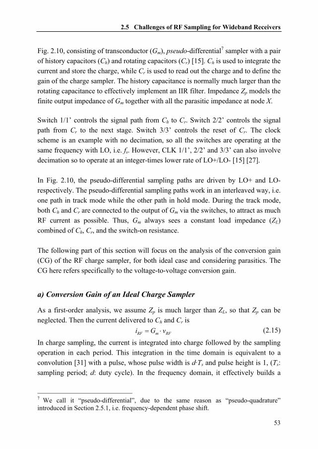
2.5 Challenges of RF Sampling for Wideband Receivers
53
Fig. 2.10, consisting of transconductor (Gm), pseudo-differential7 sampler with a pair of history capacitors (Ch) and rotating capacitors (Cr) [15]. Ch is used to integrate the current and store the charge, while Cr is used to read out the charge and to define the gain of the charge sampler. The history capacitance is normally much larger than the rotating capacitance to effectively implement an IIR filter. Impedance Zp models the finite output impedance of Gm together with all the parasitic impedance at node X. Switch 1/1’ controls the signal path from Ch to Cr. Switch 2/2’ controls the signal path from Cr to the next stage. Switch 3/3’ controls the reset of Cr. The clock scheme is an example with no decimation, so all the switches are operating at the same frequency with LO, i.e. fs. However, CLK 1/1’, 2/2’ and 3/3’ can also involve decimation so to operate at an integer-times lower rate of LO+/LO- [15] [27]. In Fig. 2.10, the pseudo-differential sampling paths are driven by LO+ and LO- respectively. The pseudo-differential sampling paths work in an interleaved way, i.e. one path in track mode while the other path in hold mode. During the track mode, both Ch and Cr are connected to the output of Gm via the switches, to attract as much RF current as possible. Thus, Gm always sees a constant load impedance (ZL) combined of Ch, Cr, and the switch-on resistance. The following part of this section will focus on the analysis of the conversion gain (CG) of the RF charge sampler, for both ideal case and considering parasitics. The CG here refers specifically to the voltage-to-voltage conversion gain.
a) Conversion Gain of an Ideal Charge Sampler
As a first-order analysis, we assume Zp is much larger than ZL, so that Zp can be neglected. Then the current delivered to Ch and Cr is
RF m RFi G v= ⋅ (2.15)
In charge sampling, the current is integrated into charge followed by the sampling operation in each period. This integration in the time domain is equivalent to a convolution [31] with a pulse, whose pulse width is d·Ts and pulse height is 1, (Ts: sampling period; d: duty cycle). In the frequency domain, it effectively builds a
7 We call it “pseudo-differential”, due to the same reason as “pseudo-quadrature” introduced in Section 2.5.1, i.e. frequency-dependent phase shift.

Chapter 2 Frequency Translation Fundamentals
54
( )sn
t n Tδ+∞
=−∞
− ⋅∑
Figure 2.11 Modeling a charge sampler with SINC transfer function
SINC transfer function H(fRF) filtering the RF input spectrum before the sampling action (see Fig. 2.11):
( ) ( ) ( )sin /sinc RF s
RF s RF sRF
d f fH f d T f d T
fπ
ππ⋅ ⋅
= ⋅ ⋅ ⋅ ⋅ ⋅ =⋅
(2.16)
To reduce the noise-and-interference aliasing, the sampling frequency should be close to the RF of the wanted signal instead of suing sub-sampling. If using zero-IF sampling, where the sampling frequency fs=1/Ts=fRF, and using 50% duty-cycle LO (d=0.5), we can get
( ) ( )sin / 2 1RF s
s s
H f ff f
ππ π
= = =⋅ ⋅
. (2.17)
If we only focus on the desired signal, the sampling operation can be seen as folding signal from RF to IF without affecting its magnitude. Thus, by combining (2.15) and (2.17), the sampled charge data can be described by
( ) min RF RF RF
s
GQ i H f vfπ
= ⋅ = ⋅⋅
. (2.18)
Charge samplers in the earlier age [31] didn’t use the rotating capacitor Cr. Instead they reset Ch every LO cycle so to define the CG via Ch only8. On the other hand, in the modern charge sampler of Fig. 2.10 [15], the combination of Ch and Cr implements an IIR low-pass filter, which makes the overall CG more complicated.
8 In that case, the down-converted voltage on Ch is well defined by the charge obtained from (2.18) divided by the value of Ch without seeing the memory effect from previous charge samples due to a reset in each LO cycle.

2.5 Challenges of RF Sampling for Wideband Receivers
55
Figure 2.12 An ideal IIR filter model in charge domain The IIR filtering effect can be understood in charge domain (Fig. 2.12). Qin is the input charge got from (2.18). Qout is the output charge carried by Cr, while Qfb is the feedback charge reserved by Ch. The coefficients α and β can be written as
; hr
h r h r
CCC C C C
α β= =+ +
. (2.19)
From (2.19) we know α=1-β. Then the charge transfer function of the IIR low-pass filter can be derived as
1 1
11 1out in inQ Q Q
Z Zα ββ β− −
−= ⋅ = ⋅
− ⋅ − ⋅. (2.20)
Then the output voltage of IF signal can be written as
1
11
out inIF
r r
Q QvC C Z
ββ −
−= = ⋅
− ⋅. (2.21)
Combining (2.18) and (2.21), we have
1 1
1 11 1
m mIFIF RF
s r RF s r
G Gvv vf C Z v f C Z
β βπ β π β− −
− −= ⋅ ⋅ ⇒ = ⋅
⋅ ⋅ − ⋅ ⋅ ⋅ − ⋅. (2.22)
The Z-domain term in the above equations determines the response of the IIR filter. If we focus on the signal down-converted from RF to DC after zero-IF sampling, we only need to know the DC response of the IIR filter. Since
1
1 1@1
DCZβ
β −
−=
− ⋅, (2.23)
we can write (2.22) into
1 mIF
RF s r
Gvv f Cπ
= ⋅⋅
. (2.24)
If we consider the pseudo-differential paths, the output signal voltage at DC will be doubled compared to the voltage of a single-ended path. Therefore, the conversion
Chapter 2 Frequency Translation Fundamentals
56
gain of an ideal RF charge sampler driven by differential LO (LO+/LO-) is
, 2IF diff mid
RF s r
v GCGv f Cπ
= = ⋅⋅
. (2.25)
Equation (2.25) is based on two assumptions: 1) zero-IF sampling, i.e. an LO frequency (fs) equal to the frequency of the input RF signal (fRF); 2) 50% duty cycle for the LO. If the RF signal after downconversion is not at DC, then the CG should also consider the RF SINC and baseband IIR filtering effect. If the LO duty cycle is not 50%, then the CG coefficient should be different from 2/π. Nevertheless, both effects can be considered via applying (2.16) for the SINC filtering and (2.20) for the IIR filtering characteristic. It may be wondered, why the CG is only determined by Cr, but not related to Ch. The CG given by (2.25) is proportional to Gm multiplied with 1/(fs·Cr). From Fig. 2.10, we can see that if modeling switched-Cr as an equivalent resistance of 1/(fs·Cr), the CG is indeed determined by the multiplication of Gm and 1/(fs·Cr) while the product of Ch and 1/(fs·Cr) affects the baseband filtering bandwidth. Therefore Cr determines the CG while the ratio of Ch and Cr affects the filtering. The following example may give some insight as well: suppose if Cr=0, which means no charge is moved out from Ch, the signal charge downconverted to DC will always accumulate and the DC voltage at Ch approaches infinity. This trend can be clearly seen from (2.25). From (2.25), it should be clear that the conversion gain is inversely proportional to fs, which is equal to fRF for zero-IF sampling. The frequency dependency of conversion gain is due to the integration feature of a charge sampler, so that the amount of charge integrated in each period depends on the time of integration. This systematic frequency dependence is undesired for a wideband receiver such as SDR, since both NF and linearity can be strongly dependent on the carrier frequency. As a comparison, for an active mixer9 with a load resistance RL, the conversion gain would be (2/π)·Gm·RL, which is not systematically dependent on fRF. In [15] and [27], a technique called temporal moving averaging (MA) is introduced 9 An interesting analogy can be found: an active down-mixer is often loaded by CL and RL to form a low-pass filter; while a charge down-sampler is loaded by Ch and an equivalent R emulated by switched-Cr which together form an IIR filter.

2.5 Challenges of RF Sampling for Wideband Receivers
57
which might be a solution. The temporal MA is the temporal integration of N RF-samples, performing a FIR filtering with N all-one coefficients and an N-times decimation (N can be defined as the decimation ratio). The charge accumulation over N samples does result in a larger conversion gain. Ideally, the gain in case of accumulation of N samples is equal to N, so
,2 m
id Ns r
GCG Nf Cπ
= ⋅ ⋅⋅
. (2.26)
From (2.26), we can see an N-times increase of input frequency might be compensated by an N-times temporal MA to keep the conversion gain stable. However, the temporal MA suffers from some problems. Due to the fact that the MA output is read out via Cr at an N-times lower rate, i.e. fs/N, there is additional aliasing with a fold-over frequency at fs/(2N). Although the intrinsic FIR filter in a MA operation generates notches to suppress the aliasing of noise and interference, the notch width is limited by N, i.e. a larger N gives a smaller notch width [27]. A narrow notch corresponds to a narrow channel bandwidth that can be protected against aliasing images. Furthermore, circuit imperfections such as the parasitics at node X also limit the achievable notch depth [27]. A limited notch depth corresponds to a limited rejection ratio of aliasing images. Therefore, an RF pre-select filter is often needed to achieve sufficient aliasing suppression around the frequency points of n·(fs/N) (n=0,1,2,3…, but n≠N), which will limit the flexibility for a SDR receiver.
b) Conversion Gain with Finite Zp
After some intuition developed via the first-order analysis in the previous part, we will include the effect of Zp for a second-order analysis in this part. A finite Zp causes a loss of gain as charge from Ch constantly leaks out through Zp every LO cycle. Therefore, it is important to understand how a finite Zp affects the conversion gain. Zp has two fundamental effects on the conversion gain of the direct RF charge sampler. One effect is charge leakage. Because of the finite impedance (Zp) to ground at node X, part of the charge stored on Ch may leak away every cycle when switching on. The other effect is current division. With this effect, the current flowing onto Ch and Cr is smaller than what got from (2.15). Actually, the effect of

Chapter 2 Frequency Translation Fundamentals
58
current division can be modeled in two steps. First, all the output current will be integrated to be a sample of charge on Ch. Second, part of this charge sample will leaks away from Zp to ground. Thus, both effects of Zp can be explained with the leakage of charge. The leakage of the remained part of all the previous charge samples on Ch represents one effect. The leakage of the current charge sample represents the other effect. The actual impact of Zp might be different depending on whether Zp is capacitive or resistive. The following analysis will discuss these two cases respectively.
Capacitive
If Zp is capacitive, it can be modeled as a capacitor Cp connected from node X to ground. Both Cp and Cr share the charge with Ch every LO cycle. If the charge on Cp is stored, there will be a charge crosstalk between the pseudo-differential paths: in an LO cycle when switching from the positive path driven by LO+ to the negative path driven by LO-, the charge from the positive path that has been stored on Cp will cancel one part of the charge on the negative path, after which another part of the charge from the negative path will be stored on Cp to cancel charge on the positive path in the next LO cycle. Therefore, if we focus on the signal downconverted from RF to DC, the amount of signal charge that is shared by Cp with the charge crosstalk effectively doubles the amount shared by Cp without the charge crosstalk. That means, due to this charge crosstalk, the effective value of Cp is doubled. To quantify the effect, an IIR filter model including the charge leakage is shown in Fig. 2.13. Qin is the input charge data got from (2.18). Qout is the output charge carried by Cr, Qfb is the feedback charge reserved by Ch, and Qleak is the leakage charge taken by Cp. The coefficients α1, α2, and β can be written as
1 2
2; ;
2 2 2p hr
h r p h r p h r p
C CCC C C C C C C C C
α α β= = =+ + + + + +
. (2.27)
Note that the effect of Cp is doubled as in (2.27). The charge transfer function of the IIR low-pass filter can be written as
1 11 1 1
1 11 1 1 1 2
rout in in in
r p
CQ Q Q QZ Z Z C C
α αβ ββ β β β− − −
− −= ⋅ = ⋅ ⋅ = ⋅ ⋅
− ⋅ − ⋅ − − ⋅ +. (2.28)

2.5 Challenges of RF Sampling for Wideband Receivers
59
Figure 2.13 An IIR filter model including charge leakage
Therefore, the output voltage of IF signal can be written as
1
12 1
out inIF
r r p
Q QvC C C Z
ββ −
−= = ⋅
+ − ⋅. (2.29)
Combining (2.18) and (2.29), we have
1
1
1( 2 ) 1
1( 2 ) 1
βπ β
βπ β
−
−
−= ⋅ ⋅
⋅ ⋅ + − ⋅
−⇒ = ⋅
⋅ ⋅ + − ⋅
mIF RF
s r p
mIF
RF s r p
Gv vf C C Z
Gvv f C C Z
. (2.30)
Again, if we focus on the signal downconverted from RF to DC, we can write (2.30) as
1( 2 )
mIF
RF s r p
Gvv f C Cπ
= ⋅⋅ +
. (2.31)
For the pseudo-differential output paths, the conversion gain will be
, 2( 2 )
IF diff m
RF s r p
v Gv f C Cπ
= ⋅⋅ +
. (2.32)
From (2.32), it should be clear that the conversion gain is, again, inversely proportional to the LO frequency fs.
Resistive
If Zp is resistive, it can be modeled as a resistor Rp connected from node X to ground. One step further, Rp can be modeled as an equivalent switched-capacitor resistor, with a capacitor CRp operating at the same frequency with LO, i.e. fs. Since Rp only connects to Ch and Cr in either positive or negative path for half of the LO

Chapter 2 Frequency Translation Fundamentals
60
period, the effective charge leakage is halved comparing to if connecting for a full period. So equivalently 2Rp should be counted if modeled as switched-CRp, and then we have the equivalent capacitor
12Rp
p s
CR f
=⋅
. (2.33)
The same IIR model as in Fig. 2.13 can be used for the case of Rp. But different from a real capacitor, the equivalent capacitor CRp does not cause any charge crosstalk, because Rp can not store charge. Therefore, the coefficients α1, α2, and β for the case of Rp should be written as
1 2; ;p
p p p
R hr
h r R h r R h r R
C CCC C C C C C C C C
α α β= = =+ + + + + +
. (2.34)
The capacitor CRp is based on (2.33). Following the same derivation steps as for the case of capacitive Zp, if we focus on the signal at DC, we can arrive at:
1 1 1( ) ( 0.5 / ) ( 1/ 2 )
p
m m mIF
RF s r R s r s p s r p
G G Gvv f C C f C f R f C Rπ π π
= ⋅ = ⋅ = ⋅⋅ + ⋅ + ⋅ +
. (2.35)
For the pseudo-differential output paths, the conversion gain will be
, 2( 1/ 2 )
IF diff m
RF s r p
v Gv f C Rπ
= ⋅⋅ +
. (2.36)
It is not directly inversely-proportional to fs as (2.25) and (2.32) due to the “1/2Rp” term, but still can be strongly dependent on fs.
Both Capacitive and Resistive
Combining (2.32) and (2.36), it can be proved that when both Cp and Rp are present, the non-ideal conversion gain is
2( 2 ) 1/ 2
mnid
s r p p
GCGf C C Rπ
= ⋅⋅ + +
. (2.37)
From (2.37), we can see that at low frequency Rp will dominate the parasitic effect and at high frequency Cp will dominate. It can also be seen that the conversion gain is just the same to an active mixer loaded with three equivalent resistors in parallel, i.e. 1/(fs·Cr), 1/(2fs·Cp), and 2Rp. With this intuition, for N-times temporal moving average, we can view the RF

2.5 Challenges of RF Sampling for Wideband Receivers
61
charge sampler as a mixer loaded by 1/(fs·Cr/N), 1/(2fs·Cp), and 2Rp in parallel. Then the complete conversion gain, considering the parasitic effects and the decimation, can be written as
( ),2
2 1 (2 )m
nid Ns r s p p
GCGf N C f C Rπ
= ⋅⋅ + ⋅ +
. (2.38)
From (2.38), we can see that the conversion gain CGnid,N can be strongly dependent on the sampling frequency, which is equal to the input RF, in the case of zero-IF sampling. If a charge leakage ratio is defined as
1
12 1 (2 )
rN
p s p
C NC f R
α−
⎛ ⎞= +⎜ ⎟⎜ ⎟+ ⋅⎝ ⎠
, (2.39)
then (2.26) and (2.38) can be connected via this ratio: )1(,, NNidNnid CGCG α−⋅= . (2.40)
Thus, to get closest to the ideal conversion gain, we need to minimize the charge leakage ratio αN. Attention should also be paid to the decimation ratio N, because a larger N means a larger αN.
c) Simulations
To verify the above analysis from (2.15) to (2.40), the circuit in Fig. 2.10 has been simulated for zero-IF downconversion, with the following settings: Gm=20mS, Ch=10pF, Cr=500fF. A buffer capacitor Cb=10pF is added at the output of each pseudo-differential path to store the charge, and it will not change the conversion gain at DC. Fig. 2.14 plots CG versus Cp and CG versus Rp with N=1 and fs=1GHz, which shows the theoretical analysis (2.38) matches very well with the simulation. From (2.38), we can see that, if we want parasitic impedance has little effect on the conversion gain, the conditions of Cr>>2Cp and Cr>>1/(2fs·Rp) have to be met simultaneously. To verify the parasitic effects versus the sampling frequency, Fig. 2.15 shows the conversion gain versus fs, comparing the non-ideal case (Rp=10kΩ, Cp=10fF) with the ideal case for both at N=1, i.e. no decimation. From Fig. 2.15, we can see that at low frequency Rp will dominate the parasitic effect and the difference from ideal case can be big while at high frequency Cp tends to dominate but its effect is small since Cr>>2Cp in this specific example.

Chapter 2 Frequency Translation Fundamentals
62
101 102 10315
20
25
30
35
40
45C
onve
rsio
n G
ain
(dB
)
10-1 100 1010
10
20
30
40
Con
vers
ion
Gai
n (d
B)
theoreticalsimulated
theoreticalsimulated
Cp (fF) Rp (kΩ) (a) (b)
Figure 2.14 Conversion gain of an RF charge sampler with finite Zp: (a) variable Cp and Rp=∞; (b) variable Rp and Cp=0
10-1 100 1010
10
20
30
40
50
idealnon-ideal theoreticalnon-ideal simulated
Figure 2.15 Conversion gain versus sampling frequency (fs) of an RF charge sampler considering parasitics

2.5 Challenges of RF Sampling for Wideband Receivers
63
0 2 4 6 8 1010
15
20
25
30
35
40
45
Decimation Ratio
Con
vers
ion
Gai
n (d
B)
idealRp=100KOhm Cp=1fF theoreticalRp=100KOhm Cp=1fF simulatedRp=10KOhm Cp=10fF theoreticalRp=10KOhm Cp=10fF simulated
Figure 2.16 Conversion gain versus decimation ratio (N) of an RF charge sampler considering different parasitics
Fig. 2.16 shows the conversion gain versus the decimation ratio (N) at 2.4GHz, for an ideal and a non-ideal RF charge sampler based on (2.26) and (2.38) respectively. Two sets of non-ideal configuration have been simulated, one set is Rp=100kΩ and Cp=1fF, which corresponds to a charge leakage ratio of roughly 1% when N=1; the other set is Rp=10kΩ, and Cp=10fF, which corresponds to a charge leakage ratio of roughly 10% when N=1. Fig. 2.16 shows the simulated results match the theoretical results very well, and N can indeed control the CG.
d) Discussions
A major contributor of Rp can be the output resistance of Gm. For Cp, there might be several contributors, such as the output capacitor of Gm and the parasitic capacitor of switches. When AC coupling capacitor is used between the output of Gm and the sampling switches, its parasitic capacitance can be a major concern.
Consequences
Since the variation of conversion gain will change the NF contribution of later

Chapter 2 Frequency Translation Fundamentals
64
stages, the finite impedance at node X, i.e. Zp=Rp//Cp, has a direct impact on the receiver sensitivity. To achieve a maximum sensitivity, we should maximize Zp, i.e. minimize Cp and maximize Rp. While for a smaller conversion gain, e.g. in the automatic-gain-control (AGC) application, we might sometimes want a smaller Zp. Other than the conversion gain, Zp can also affect filter characteristics. For instance, if we look at (2.27), the feedback factor β will be lower when Cp is larger and similarly when Rp is smaller based on (2.34). A lower β means a larger -3dB bandwidth of the IIR filter. As another example, if the decimation is performed on the sampling stage, the charge leakage caused by Cp and Rp will reduce the notch depth introduced by the moving-average FIR filter [27]. Therefore, the performance of the aliasing rejection before decimation is degraded. Note that the effects on FIR and IIR filters reflect the impact of Zp on the receiver selectivity. Overall, the impedance Zp at node X should be well controlled because of its critical effects on both sensitivity and selectivity.
Potential Solutions
Equation (2.38) shows the frequency dependency in a general sense. But more than that, it also suggests some potential solutions. For example, we can tune the parameters such as Gm, Cr, Cp, Rp, or N to compensate for the dependence of the CG on fs. From (2.38), we can see temporal moving average is possible to be used to tune the conversion gain by changing N. However, to make it effective, we have to minimize Cp, while the impact of Rp is not frequency dependent. In the mean time, as mentioned at the end of part a), the limited notch width due to the nature of FIR filter might block its application in some wide-channel communication standards. Therefore, for multi-stand RF-sampling receiver which should be able to accommodate any useful channel bandwidth, at least a selective IIR filter, together with the moving-average FIR filter, is preferred before any decimation. The other solutions come by adding programmability to the receiver. For example, we can make a bank of transconductors which is programmable via switches for multi-band capability. The whole frequency range of input signal can be divided

2.6 Conclusions
65
into several sub-bands. The activated Gm can be tuned for different sub-bands to keep the conversion gain almost flat. Of course, the conversion gain will still have some variation within each sub-band, but this variation can be acceptable if the covering range of each sub-band has been chosen to be sufficiently small. Similarly, programmable Cp or Cr can also be used. But programmability means added design complexity. It might also cost extra power and area. Fortunately, this programmability can also be used to play the role of an RF variable-gain amplifier (VGA). So the extra cost of complexity can be reduced, by merging the RF charge sampler and the RF VGA. Interestingly, as shown by (2.38), since the CG’s dependence on Rp is frequency-independent, if let Rp dominate the CG definition instead of Cr or Cp, the CG’s frequency dependency can be negligible. Anyhow, to solve the frequency-dependent CG property of charge sampling can take lots of efforts. On the other hand, voltage sampling does not have this undesired property and for this point it seems to be more compatible with wideband applications. More serious noise and interference folding associated with voltage sampling can be alleviated via DT mixing technique (Fig 2.4 (b)) with wideband harmonic rejection that will be introduced in Chapter 3.
2.6 Conclusions For feasibility and lower power consumption, frequency translation (FT) is highly desired in radio transceivers. This chapter focuses on the fundamental differences among FT techniques for radio receivers, mainly for downconversion. The discussion is carried out in four parts. 1) We showed that downconversion techniques can be classified based on the type of input signal on the one hand, i.e. continuous versus discrete both in time and amplitude, and the downconversion principle on the other, i.e. mixing or sampling. Besides five techniques which are already known, the classification also leads to the definition of a DT-mixing technique that operates on continuous-amplitude but discrete-time samples which can be obtained from CT-to-DT sampling. This

Chapter 2 Frequency Translation Fundamentals
66
technique will be extended in Chapter 3. 2) To clarify the classification, the fundamental distinctions between the mixing and the sampling principles are discussed in both time and frequency domain. Compared to mixing, sampling always changes the information rate in the time domain but not necessarily results in frequency translation in the frequency domain. It is mathematically shown that CT-to-DT conversion is important for sampling to achieve a well-defined gain. 3) Based on the classification, three receiver architectures are defined: an RF-mixing receiver, an RF-sampling receiver, and an ideal SWR receiver. The ideal SWR receiver is most flexible but not yet feasible for frequencies above a few hundred MHz. The suitability of RF-mixing and RF-sampling receivers for SDR is then discussed, arguing that both can be suitable. While RF sampling can have advantages with respect to the compatibility with the CMOS scaling and the SoC integration, it comes at the cost of extra complexity due to the clock generation/routing and the RF-related baseband processing. With the CMOS scaling and SoC trend, it can be relevant to explore the potential of RF-sampling receivers for SDR applications. 4) Compared to RF mixing, traditional RF-sampling techniques present extra challenges for wideband receivers. Therefore, we identified three challenges: frequency-dependent phase shift, aliasing of noise and interference, and frequency-dependent conversion gain of charge sampling. Their effects are analyzed quantitatively and verified via simulations. The frequency-dependent phase shift is due to the fact that sampling naturally uses delay to approximate phase shift. Voltage sampling seriously suffers from aliasing due to equal-magnitude harmonic sampling tones. Due to integration, charge sampling can have a reduced aliasing effect similar to CT mixing. However, also due to integration, charge sampling presents frequency-dependent conversion gain. A quantitative analysis for an RF charge sampler considering parasitic effects and a certain decimation ratio has been verified. In Chapter 3, we will show that these challenges can be addressed by applying voltage sampling followed by the proposed DT-mixing technique with wideband phase shift and wideband harmonic rejection.
2.7 References
67
2.7 References [1] Z. Ru, E. Klumperink, B. Nauta, “Discrete-Time Mixing Receiver
Architecture for RF-Sampling Software-Defined Radio”, submitted to IEEE J. Solid-State Circuits
[2] Z. Ru, E. Klumperink, B. Nauta, "On the Suitability of Discrete-Time Receivers for Software-Defined Radio", IEEE ISCAS, Proc., pp.2522-2525, May 2007
[3] R. Pullela, S. Tadjpour, D. Rozenblit, et. al., "An integrated closed-loop polar transmitter with saturation prevention and low-IF receiver for quad-band GPRS/EDGE", IEEE ISSCC, Dig. Tech. Papers, pp.112-113,113a, Feb. 2009
[4] R. Bagheri, A. Mirzaei, S. Chehrazi, "An 800MHz to 5GHz Software-Defined Radio Receiver in 90nm CMOS", IEEE ISSCC, Dig. Tech. Papers, pp.1932-1941, Feb. 2006
[5] E. Alpman, H. Lakdawala, L.R. Carley, K. Soumyanath, "A 1.1V 50mW 2.5GS/s 7b Time-Interleaved C-2C SAR ADC in 45nm LP digital CMOS", IEEE ISSCC, Dig. Tech. Papers, pp.76-77,77a, Feb. 2009
[6] R.C. Taft, P.A. Francese, M.R. Tursi, et. al., "A 1.8V 1.0GS/s 10b self-calibrating unified-folding-interpolating ADC with 9.1 ENOB at Nyquist frequency", IEEE ISSCC, Dig. Tech. Papers, pp.78-79,79a, Feb. 2009
[7] B. Murmann, "ADC Performance Survey 1997-2009", [Online], Available: http://www.stanford.edu/~murmann/adcsurvey.html
[8] Y. Tsividis, "Digital signal processing in continuous time: a possibility for avoiding aliasing and reducing quantization error," IEEE International Conference on Acoustics, Speech, and Signal Processing (ICASSP), Proceedings of, vol.2, no., pp. ii-589-92 vol.2, May 2004
[9] B. Schell, Y. Tsividis, "A Continuous-Time ADC/DSP/DAC System With No Clock and With Activity-Dependent Power Dissipation", IEEE J. Solid-State Circuits, vol.43, no.11, pp.2472-2481, Nov. 2008
[10] Z. Ru, E. Klumperink, B. Nauta, "A Discrete-Time Mixing Receiver Architecture with Wideband Harmonic Rejection," IEEE ISSCC, Dig. Tech. Papers, pp.322-616, Feb. 2008
[11] A.R. Shahani, D.K. Shaeffer, and T.H. Lee, "A 12-mW wide dynamic range CMOS front-end for a portable GPS receiver", IEEE J. Solid-State Circuits, vol.32, no.12, pp.2061-2070, Dec. 1997
[12] M. Soer, E. Klumperink, Z. Ru, F. van Vliet, and B. Nauta, “A 0.2-to-2.0GHz

Chapter 2 Frequency Translation Fundamentals
68
CMOS Receiver without LNA achieving >11dBm IIP3 and <6.5dB NF”, IEEE ISSCC, Dig. Tech. Papers, Feb. 2009
[13] D. Jakonis, K. Folkesson, J. Dbrowski, et. al., "A 2.4-GHz RF sampling receiver front-end in 0.18-μm CMOS", IEEE J. Solid-State Circuits, vol.40, no.6, pp. 1265-1277, June 2005
[14] H. Pekau, J.W. Haslett, "A 2.4 GHz CMOS sub-sampling mixer with integrated filtering", IEEE J. Solid-State Circuits, vol.40, no.11, pp. 2159-2166, Nov. 2005
[15] R.B. Staszewski, K. Muhammad, D. Leipold, et. al., "All-digital TX frequency synthesizer and discrete-time receiver for Bluetooth radio in 130-nm CMOS", IEEE J. Solid-State Circuits, vol.39, no.12, pp. 2278-2291, Dec. 2004
[16] K. Muhammad, H. Yo-Chuol, T.L. Mayhugh, et. al., "The First Fully Integrated Quad-Band GSM/GPRS Receiver in a 90-nm Digital CMOS Process", IEEE J. Solid-State Circuits, vol.41, no.8, pp.1772-1783, Aug. 2006
[17] R.B. Staszewski, D. Leipold, O. Eliezer, et. al., "A 24mm2 Quad-Band Single-Chip GSM Radio with Transmitter Calibration in 90nm Digital CMOS", IEEE ISSCC, Dig. Tech. Papers, pp.208-607, Feb. 2008
[18] F. Montaudon, R. Mina, S. Le Tual, et. al., "A Scalable 2.4-to-2.7GHz Wi-Fi/ WiMAX Discrete-Time Receiver in 65nm CMOS", IEEE ISSCC, Dig. Tech. Papers, pp.362-619, Feb. 2008
[19] B. Leung, “VLSI for Wireless Communication”, Prentice Hall, Upple Saddle River, NJ 2002
[20] V.J. Arkesteijn, E.A.M. Klumperink, B. Nauta, "Jitter requirements of the sampling clock in software radio receivers", IEEE Trans. Circuits and Systems II: Express Briefs, vol.53, no.2, pp. 90-94, Feb. 2006
[21] J. Craninckx, M. Liu, D. Hauspie, et. al., "A Fully Reconfigurable Software-Defined Radio Transceiver in 0.13μm CMOS", IEEE ISSCC, Dig. Tech. Papers, pp.346-607, Feb. 2007
[22] V. Giannini, P. Nuzzo, C. Soens, et. al., "A 2mm2 0.1-to-5GHz SDR receiver in 45nm digital CMOS", IEEE ISSCC, Dig. Tech. Papers, pp.408-409, Feb. 2009
[23] M. Kitsunezuka, S. Hori, T. Maeda, "A Widely-Tunable Reconfigurable CMOS Analog Baseband IC for Software-Defined Radio", IEEE ISSCC, Dig. Tech. Papers, pp.66-595, Feb. 2008
[24] H. Darabi, A. Zolfaghari, H. Jensen, J. Leete, B. Mohammadi, J. Chiu, et. al., "A Fully Integrated Quad-Band GPRS/EDGE Radio in 0.13μm CMOS", IEEE

2.7 References
69
ISSCC, Dig. Tech. Papers, pp.206-607, Feb. 2008 [25] L.R. Carley, T. Mukherjee, "High-speed low-power integrating CMOS
sample-and-hold amplifier architecture", IEEE CICC, Proc., pp.543-546, May 1995
[26] S. Karvonen, T.A.D. Riley, S. Kurtti, J. Kostamovaara, "A quadrature charge-domain sampler with embedded FIR and IIR filtering functions", IEEE J. Solid-State Circuits, vol.41, no.2, pp. 507-515, Feb. 2006
[27] K. Muhammad, R.B. Staszewski, "Direct RF sampling mixer with recursive filtering in charge domain", IEEE ISCAS, Proc, pp. I-577-80 Vol.1, May 2004
[28] L. Joet, A. Dezzani, F. Montaudon, F. Badets, F. Sibille, C. Corre, et. al., "Advanced `Fs/2' Discrete-Time GSM Receiver in 90-nm CMOS", IEEE ASSCC, pp.371-374, Nov. 2006
[29] A. J. Coulson, “A generalization of nonuniform bandpass sampling”, IEEE Trans. Signal Processing, vol. 43, pp. 694–704, Mar. 1995.
[30] M. Valkama, M. Renfors, "A novel image rejection architecture for quadrature radio receivers", IEEE Trans. Circuits and Systems II: Express Briefs, vol.51, no.2, pp. 61-68, Feb. 2004
[31] G. Xu, J. Yuan, "Performance analysis of general charge sampling", IEEE Trans. Circuits and Systems II: Express Briefs, vol.52, no.2, pp. 107-111, Feb. 2005

Chapter 2 Frequency Translation Fundamentals
70

71
Chapter 3 Discrete-Time Mixing Receiver for RF-Sampling SDR The previous chapter compared RF-mixing receivers and RF-sampling receivers, and concluded both can be suitable for software-defined radio but with different advantages and drawbacks. To benefit from RF sampling’s advantages such as the compatibility with CMOS scaling and SoC integration, this chapter will explore the potential of RF sampling for SDR applications, by proposing a new frequency translation technique, i.e. discrete-time (DT) mixing [1] [2]. After the introduction in Section 3.1, Section 3.2 presents the DT-mixing concept which is defined after the classification of FT techniques in Section 2.2. It aims to solve the problems of traditional RF sampling for wideband receivers identified in Section 2.5 by its wideband features. To verify the concept, Section 3.3 presents an implementation of DT-mixing downconverter, with 8-times oversampling and 2nd-to-6th harmonic rejection for the 200-to-900MHz RF band. It is fabricated in 65nm CMOS with simulation and measurement results presented in Section 3.4. Conclusions are drawn in Section 3.5 and references are attached in Section 3.6.
3.1 Introduction RF-sampling receivers have recently drawn both academic [3] [4] and industrial interests [5]-[8]. They sample the signal early in the receiver chain before or simultaneously with downconversion, instead of after downconversion, as done in conventional RF-mixing receivers. Direct RF sampling provides the potential to move A/D converters (ADC) closer to antenna aiming at an ideal software radio.

Chapter 3 Discrete-Time Mixing Receiver for RF-Sampling SDR
72
Several CMOS ICs have been published in recent years to demonstrate some features suitable for SDR receivers, e.g. [9] and [10], which use wideband front-ends based on RF mixing. On the other hand, traditional RF sampling [3]-[8] is not directly suitable for SDR, as it only provides narrowband quadrature demodulation due to the frequency-dependent phase shift and narrowband1 harmonic rejection which can not protect aliasing for wideband applications. For a flexible SDR receiver, any useful channel bandwidth (BW) should be accommodated. Therefore wideband quadrature demodulation is desired to detect wideband signals and to provide wideband image rejection. Also, wideband harmonic rejection is highly desired to prevent aliasing of wideband interference or strong out-of-channel interference. This chapter describes a discrete-time mixing architecture, featuring wideband quadrature demodulation and wideband2 harmonic rejection. We will start with describing the DT-mixing concept and its wideband features. To verify the concept, we present a prototype downconverter in 65nm CMOS targeting at cognitive radio (CR) applications in TV bands [11]. The wideband features of DT mixing can be useful for the CR applications which might use non-contiguous segments of free spectrum distributed over a wide band.
3.2 Discrete-Time Mixing Receiver Concept Modern CMOS technology offers excellent switches and digital gates whose switching speed is faster in each new process generation. This feature makes it feasible to realize RF sampling, as demonstrated by some narrowband RF-sampling receivers [3]-[8]. Fig. 3.1 (a) shows a traditional RF-sampling receiver, including RF pre-select filter, LNA, RF sampler, a chain of SC circuits for filtering and decimation, IF amplifier (IFA), and ADC. However, as identified in Section 2.5, the traditional RF-sampling receivers face a few challenges to apply to wideband receivers, including 1) the frequency-dependent phase shift, leading to a narrowband quadrature demodulation; 2) the noise and interference folding due to aliasing; 3) frequency-dependent conversion gain of charge sampling. 1 Both “narrowband” here mean narrow channel bandwidth. 2 Both “wideband” here mean wide channel bandwidth.

3.2 Discrete-Time Mixing Receiver Concept
73
I
Q
SLNA
S
S
I
Q
( )sn
t n Tδ+∞
=−∞
− ⋅∑
( )sn
t n T tδ+∞
=−∞
− ⋅ − Δ∑
x(t)x(t)
I
Q
ToDigital
N
N IFA
IFA ADC
ADC
SLNA SC Filter(a)
(b)
Figure 3.1 (a) Block diagram of a traditional RF-sampling receiver; (b) Traditional RF-sampling receiver using a time delay (Δt) for quadrature demodulation
The last point can be alleviated by applying voltage sampling whose voltage-to-voltage conversion gain is not systematically dependent on frequency. For the other two challenges, we will present an architecture-level solution, namely DT mixing, which allows both wideband quadrature demodulation and wideband harmonic rejection to reduce aliasing. Next, we will address these two problems one by one.
3.2.1 Wideband Quadrature Demodulation
A traditional RF-sampling receiver uses a time delay (shift) ∆t between two sampling paths, which is also called second-order sampling [12], to approximate a desired phase shift such as 90°, as shown in Fig. 3.1 (b). The resulted phase shift between I and Q paths was given in Section 2.5.1:
2 RFf tϕ πΔ = ⋅ ⋅Δ . (3.1)
From (3.1) we can see for a fixed ∆t, the phase shift ∆φ is dependent on fRF, i.e. frequency-dependent phase shift. An exact ∆φ can only be obtained at specific
Chapter 3 Discrete-Time Mixing Receiver for RF-Sampling SDR
74
frequency points. For instance, an exact 90° is only achieved at frequencies of (k+0.25)/Δt where k is an integer. Generally ∆t can be chosen in such a way that the phase shift is exact for the center frequency (fc) of the desired RF signal. Rearranging (3.1), we get ∆t=∆φ/(2π·fRF). For a 90° phase shift, i.e. ∆φ=π/2+k·2π, the following condition holds:
/ 2 2 0.252 c c
k ktf f
π ππ+ ⋅ +
Δ = = . (3.2)
The absolute phase error at frequency fRF can be described as 2 ( )e RF cf f tϕ π= ⋅ − ⋅Δ . (3.3)
Larger phase error leads to less accurate quadrature demodulation and degraded image rejection. For SDR applications aimed to accommodate any standards, such a systematic phase error is clearly undesired. Since the phase error can be predicted as (3.3), it can be corrected using digital compensation [13] at the cost of extra power and complexity. On the other hand, the phase shift introduced by mixing is theoretically constant over frequency since the multiplication operation conveys the phase from the LO to the IF signal. We propose to retain this favorable property of mixing in an RF-sampling receiver, via a discrete-time mixing architecture. The basic DT-mixing downconverter is shown in Fig. 3.2. It consists of a sampler followed by a DT mixer. The sampler running at fs converts the RF signal centered at fc from CT to DT domain. In principle, there is no specific requirement on the ratio of fs/fc, i.e. subsampling, Nyquist sampling and oversampling are all possible. Assume the signal frequency after sampling is f0, sampled at a rate of fs. The relationship f0≤fc holds, as a result of sampling. In the DT mixer the signal is mixed down from f0 to fIF, with a DT sine-wave of frequency f1 and which is also sampled at fs. The relationship fIF=|f0-f1| holds, as a result of down-mixing. Note that downconversion may happen in both the sampler and the DT mixer stages.

3.2 Discrete-Time Mixing Receiver Concept
75
Figure 3.2 A basic discrete-time mixing downconverter
Figure 3.3 A discrete-time (DT) mixing downconverter using I/Q DT mixers
For I/Q DT mixing, as shown in Fig. 3.3, a single sampling stage converts a CT signal into the DT domain, followed by two DT mixers multiplying the sampled signal with a DT cosine-wave and a DT sine-wave respectively. For zero-IF downconversion, the DT cosine or sine frequency f1 is the same as the signal center frequency f0 after sampling, i.e. f1=f0. The DT cosine and sine waves have a 90° phase difference, transferred to IF via multiplication, similar to what a CT mixer does. In contrast to the traditional DT receivers generating a phase difference via a delay, the 90° phase shift by I/Q DT mixing is frequency independent, leading to a true wideband quadrature demodulation and wideband image rejection.

Chapter 3 Discrete-Time Mixing Receiver for RF-Sampling SDR
76
350 400 450 500 550 600 65070
75
80
85
90
95
100
105
110
Input Frequency (MHz)
Phas
e Sh
ift (d
eg)
DT MixingSampling
Figure 3.4 Phase shift over input RF at 500MHz LO, generated via quadrature demodulation of DT mixing and traditional RF sampling
We simulated a 500MHz RF signal down-converted to quadrature zero-IF by a traditional RF-sampling receiver and our proposed DT-mixing receiver. The phase shifts for the two approaches are compared in Fig. 3.4, for a 100MHz IF-span, showing almost a 20° error from the traditional approach while maintaining wideband flat 90° via our proposed approach.
3.2.2 Wideband Harmonic Rejection
Another challenge of an RF-sampling receiver is aliasing, e.g. noise and interference around harmonics of the LO are folded to baseband during the sampling process. For narrowband applications, a dedicated RF filter is often used (Fig. 3.1 (a)) so aliasing is not a problem. However, for SDR applications, such a filter may limit the flexibility and therefore undesired. We need to find other solutions to at least relax the requirement on the RF filter.

3.2 Discrete-Time Mixing Receiver Concept
77
DT sine1
1+√2
-(1+√2)
-1
1√2
(a)
(b)
fc0
fc0
Tc/4
Tc
Tc/8Tc=8·Ts
Ts
fc=1/Tc, fs=1/Ts
2fc 3fc 4fc 5fc 6fc 7fc 8fc
2fc 3fc fs/2 5fc 6fc 7fc fs
Figure 3.5 Effective LO waveform in one period for 2nd to 6th harmonic
rejection and the corresponding spectrum: (a) continuous-time; (b) discrete-time For CT mixer, it is well-known that all even-order harmonics can be rejected by applying a differential LO. Moreover, in [14], a harmonic-rejection (HR) technique for CT mixers in a transmitter was proposed to suppress some odd-order harmonics. The basic principle of HR is, using a sum of weighted square-wave signals, to build an effective LO that is closer to a sine-wave, so to reduce the amount of harmonics in the effective LO. For example, as shown in Fig. 3.5 (a), an effective LO summed from three time-shifted square-waves with an amplitude ratio of 1:√2:1 is free of the 2nd to 6th harmonics, and only contains the (8n±1)th harmonics (n=0, 1, 2…so only 1st, 7th, 9th…). A similar idea can be applied to the DT mixer to reject sampling aliases. Since the DT sine-wave has the sampling alias located at (n·fs±fIF), the higher the sample rate, the less the amount of in-band aliases, for a given RF-filter BW. So oversampling (fs>2fRF) is more effective. For zero-IF downconversion, we can choose fs=m·fc (m=1, 2, 3…). The remaining harmonics causing aliasing are the (m·n±1)th, and the first un-wanted harmonic is the (m-1)th. The further-away the first unwanted harmonic, i.e. a larger m, the less requirements on the RF filter. Fig. 3.5 (b) shows an example of the DT sine-wave with m=8, corresponding to Fig. 3.5 (a).
Chapter 3 Discrete-Time Mixing Receiver for RF-Sampling SDR
78
A FIR filter on signal path can also be used to reject sampling aliases by positioning the filter notches at the targeted alias frequencies [15]. However, it is only effective for a limited channel BW due to the limited notch BW intrinsic to any FIR filters. For SDR applications, any useful channel BW should be accommodated, so a good HR ratio over a wide channel BW is important. Wideband HR is also important to reduce the distortion caused by strong out-of-channel interferers. Therefore, a FIR-filter based HR receiver does not suit SDR applications. In contrast, the DT-mixing based HR principle does not have intrinsic channel BW limitation, i.e. presenting wideband HR, just like the HR is also wideband in a CT mixer. The wideband HR will be verified later in Section 3.4.2. Besides improving signal-to-interference ratio, oversampling and harmonic rejection in a sampling receiver will also improve signal-to-noise ratio (or equivalently NF) since the noise folding is also reduced, in the same way as rejecting interference. As a summary of this section, we proposed an alternative receiver architecture using RF sampling followed by DT mixing with a sampled cosine or sine wave. It enables wideband quadrature demodulation and wideband harmonic rejection, making RF sampling more suitable for SDR receivers. 3.3 Proof-of-Concept Implementation To prove the concept of DT mixing, we implemented a prototype receiver to cover 0.2 to 0.9GHz RF range, targeting at the cognitive radio application recently proposed in the TV band [11]. The wideband features of DT mixing can be useful for CR applications which might use non-contiguous segments of free spectrum distributed over a wide band.
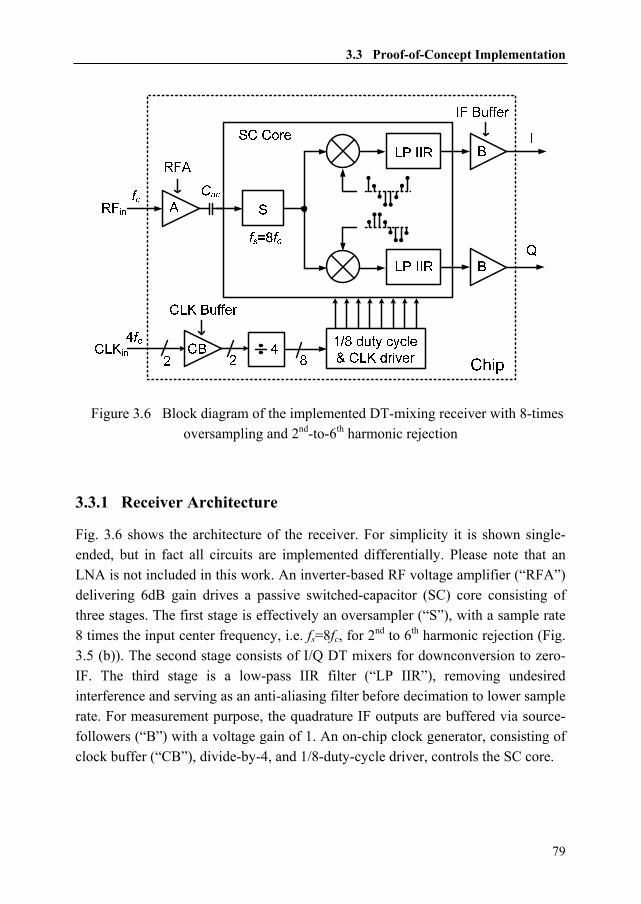
3.3 Proof-of-Concept Implementation
79
Figure 3.6 Block diagram of the implemented DT-mixing receiver with 8-times oversampling and 2nd-to-6th harmonic rejection
3.3.1 Receiver Architecture
Fig. 3.6 shows the architecture of the receiver. For simplicity it is shown single-ended, but in fact all circuits are implemented differentially. Please note that an LNA is not included in this work. An inverter-based RF voltage amplifier (“RFA”) delivering 6dB gain drives a passive switched-capacitor (SC) core consisting of three stages. The first stage is effectively an oversampler (“S”), with a sample rate 8 times the input center frequency, i.e. fs=8fc, for 2nd to 6th harmonic rejection (Fig. 3.5 (b)). The second stage consists of I/Q DT mixers for downconversion to zero-IF. The third stage is a low-pass IIR filter (“LP IIR”), removing undesired interference and serving as an anti-aliasing filter before decimation to lower sample rate. For measurement purpose, the quadrature IF outputs are buffered via source-followers (“B”) with a voltage gain of 1. An on-chip clock generator, consisting of clock buffer (“CB”), divide-by-4, and 1/8-duty-cycle driver, controls the SC core.
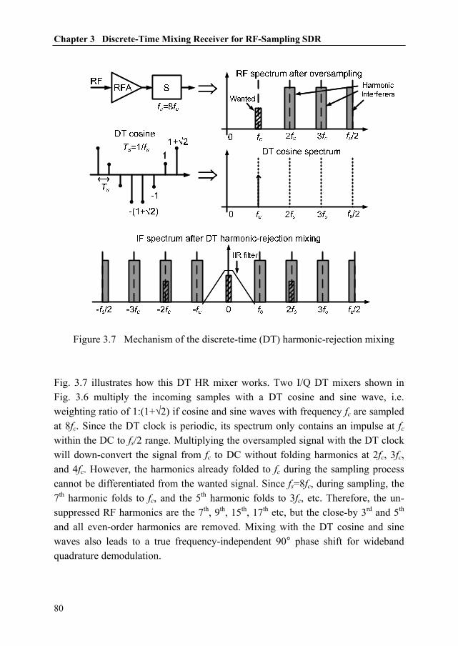
Chapter 3 Discrete-Time Mixing Receiver for RF-Sampling SDR
80
⇒
⇒
⇒
⇒
Figure 3.7 Mechanism of the discrete-time (DT) harmonic-rejection mixing
Fig. 3.7 illustrates how this DT HR mixer works. Two I/Q DT mixers shown in Fig. 3.6 multiply the incoming samples with a DT cosine and sine wave, i.e. weighting ratio of 1:(1+√2) if cosine and sine waves with frequency fc are sampled at 8fc. Since the DT clock is periodic, its spectrum only contains an impulse at fc
within the DC to fs/2 range. Multiplying the oversampled signal with the DT clock will down-convert the signal from fc to DC without folding harmonics at 2fc, 3fc, and 4fc. However, the harmonics already folded to fc during the sampling process cannot be differentiated from the wanted signal. Since fs=8fc, during sampling, the 7th harmonic folds to fc, and the 5th harmonic folds to 3fc, etc. Therefore, the un-suppressed RF harmonics are the 7th, 9th, 15th, 17th etc, but the close-by 3rd and 5th and all even-order harmonics are removed. Mixing with the DT cosine and sine waves also leads to a true frequency-independent 90° phase shift for wideband quadrature demodulation.
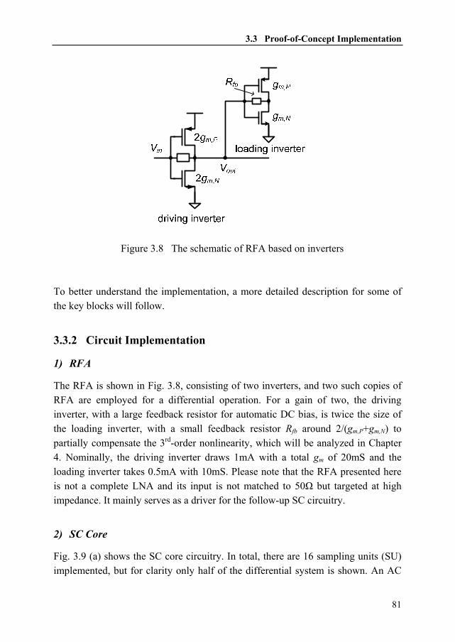
3.3 Proof-of-Concept Implementation
81
Figure 3.8 The schematic of RFA based on inverters
To better understand the implementation, a more detailed description for some of the key blocks will follow.
3.3.2 Circuit Implementation
1) RFA
The RFA is shown in Fig. 3.8, consisting of two inverters, and two such copies of RFA are employed for a differential operation. For a gain of two, the driving inverter, with a large feedback resistor for automatic DC bias, is twice the size of the loading inverter, with a small feedback resistor Rfb around 2/(gm,P+gm,N) to partially compensate the 3rd-order nonlinearity, which will be analyzed in Chapter 4. Nominally, the driving inverter draws 1mA with a total gm of 20mS and the loading inverter takes 0.5mA with 10mS. Please note that the RFA presented here is not a complete LNA and its input is not matched to 50Ω but targeted at high impedance. It mainly serves as a driver for the follow-up SC circuitry.
2) SC Core
Fig. 3.9 (a) shows the SC core circuitry. In total, there are 16 sampling units (SU) implemented, but for clarity only half of the differential system is shown. An AC

Chapter 3 Discrete-Time Mixing Receiver for RF-Sampling SDR
82
⇔
Figure 3.9 (a) Switched-capacitor (SC) core circuitry with 8-phase clock waveform; (b) Transistor-level construction of a sampling unit (SU)
coupling capacitor (Cac=2.5pF) is used between RFA and the SC core input as shown in Fig. 3.6, so that the sampling units can work at a common-mode (CM) level close to ground (GND) while the clock (L0-L7) swings from GND to VDD to minimize the switch-on resistance of NMOS switches. Four buffer capacitors Cb (18pF each) are used to store the signal charge for quadrature outputs, built via NMOS accumulation capacitors.

3.3 Proof-of-Concept Implementation
83
Fig. 3.9 (b) shows a SU in detail. In each SU, there are two weighted sampling capacitors to map the 1:(1+√2) weighted pulse amplitudes needed for a DT cosine or sine wave. In previous work, weighted amplifiers were used [9] [14] [15]. We exploit weighted capacitors which can have superior matching properties. To make a non-integer 1:(1+√2) ratio reliable in layout is difficult. We used unit capacitors with value Csu in a 2:5 ratio as approximation (C1=2Csu=160fF, C2=5Csu=400fF), built via metal-oxide-metal (MOM) capacitors. In each sampling unit, there are three pairs of switches controlled by three different clock phases, and in each pair the two switches also share the same weighting factor as the two capacitors. The switch pair for sampling (“sampling switches”) is controlled by CLKin, and the switch pair for DT mixing (“mixing switches”) is controlled by CLKout. The third switch pair for reset (“reset switches”) controlled by CLKres defines the CM level of all switches to GND. The working procedure of a sampling unit is as follows, taking the upper left unit in Fig. 3.9 (a) as an example:
1) at clock phase L0 (CLKin high), the sampling switches take the same RF voltage to two sampling capacitors C1 and C2;
2) then the charge will be kept for three idle phases, and at phase L4 (CLKout
high) the two charge samples will be transferred via the “mixing switches” to two buffer capacitors Cb, one in I path (I+ side) and the other in Q path (Q- side);
3) waiting for another idle phase, in phase L6 (CLKres high) the reset switches clean up the sampling capacitors C1 and C2;
4) and after one more idle phase, the whole procedure repeats from phase L0. The other 7 units experience the same pattern of activity but shifted in time. By inserting some idle phases between each operation (sampling, mixing, or reset), we can guarantee the three switching operations do not disturb each other. Next we will describe each functional blocks, i.e. the sampler, the DT mixer, and the IIR filter, in the SC core of Fig. 3.6.
a) Sampler
We aim for a voltage sampling downconverter, which suffers from severe noise

Chapter 3 Discrete-Time Mixing Receiver for RF-Sampling SDR
84
DE
MU
X
Figure 3.10 To implement discrete-time mixing via de-multiplexing folding. Oversampling can reduce the noise folding and hence improve NF. The oversampling function is implemented via a time-interleaved sampling structure. Eight interleaved sampling units are controlled by 8-phase non-overlapping clocks with 1/8 duty cycle, as shown in Fig. 3.9 (a). Each of the 8-phase clocks gives a sample rate of fc, and altogether an effective sample rate of 8fc is achieved. Using time-interleaved sampling to achieve oversampling, there is no extra cost on clock speed compared to other HR systems [9] [14] [15], where multiphase clocks are also employed.
b) DT Mixer
The DT mixing is implemented in the charge domain, via a systematic combination of the mixing switches from all sampling units to transfer the charge samples from the sampling capacitors (C1, C2) to the buffer capacitors (Cb). Effectively the DT mixing is realized via de-multiplexing as shown in Fig. 3.10. The oversampled charge data stream RF(k) goes through the switching network controlled by CLKout in Fig. 3.9 (b) and becomes IF(k). For illustration, Fig. 3.10 actually shows an example with a DC input RF(k) which is up-converted to become a quadrature DT sinusoidal output IF(k). But the same principle applies to downconversion. Changing the initial phase of the DT cosine and sine, the resulting LO waveform can be different, leading to a different ratio among sampling capacitors. As shown

3.3 Proof-of-Concept Implementation
85
Figure 3.11 Choosing initial phases of DT cosine and sine: why π/8
in Fig. 3.11, by choosing the initial phase to be π/8, we have cos(2 /8 / 8) sin(2 / 8 / 8) constantk kπ π π π⋅ + + ⋅ + = . (3.4)
This choice guarantees the identical loading for all clock phases without extra dummy needed. Conversion gain (CG) is an important property of a mixer. A general DT mixer model for calculating the CG is given in Fig. 3.12, where the mixing is modeled in the charge domain. The figure shows the whole chain of the SC core, but we only derive CG of the DT mixer (in the dashed-line box) while the voltage gain of an ideal voltage sampler and an IIR filter is known to be 1. An equivalent capacitor Cin at the input of the DT mixer converts voltage into charge, an equivalent capacitor Cout at the output converts charge back into voltage. The voltage gain is proportional to their ratio Cin/Cout due to charge conservation from input to output. Please note that the “resetting” operation in a sampling unit (Fig. 3.9 (b)) does not affect the charge conservation principle here since it occurs after the “mixing” operation. The charge that is erased by “resetting” is the residue charge after the IIR operation.

Chapter 3 Discrete-Time Mixing Receiver for RF-Sampling SDR
86
Figure 3.12 Block diagram of the SC core using a charge-domain model for the DT mixer (in the dashed-line box)
Multiplying with a DT sine-wave sin(2πk·f1/fs+φ) with an amplitude of 1, the loss is 0.5 since the output signal amplitude at the difference frequency is halved compared to the input. Taking this into account, the voltage CG of a DT mixer can be expressed as
,
,
0.5IF k in
RF k out
V CCGV C
= = , (3.5)
where VIF,k and VRF,k represent the amplitude of the IF data VIF(k) and the sampled RF data VRF(k) respectively. To develop some insight, we may compare (3.5) to the voltage CG in a CT current-commutating mixer, where a transconductor gm or a resistor Rin can be used for voltage-to-current conversion, and a load resistor RL can be used for current-to-voltage conversion. The role of gm or 1/Rin is like the role of Cin here for voltage-to-charge conversion, and the role of RL is like the role of 1/Cout here for charge-to-voltage conversion. The value of Cin and Cout in (3.5) depends on the specific implementation. But in general, Cin and Cout are defined by the sampling capacitor together with the function before and after the DT mixer respectively. First we derive Cout. In our prototype shown in Fig. 3.6, the DT mixer is followed by an IIR filter, thus Cout is the same as the equivalent capacitor seen by the IIR filter, i.e. Cout=CIIR ≈(C1+C2)/2 as will be derived following (3.8). Now we derive Cin. Note that the amplitude of the DT sine-wave in Fig. 3.5 (b) is √(4+2√2). Assume p1 and p2 are the weighting factors in a DT sine-wave whose amplitude is 1 (so p1≤1 and p2≤1). Since we use the sampling capacitors to realize

3.3 Proof-of-Concept Implementation
87
these weighting factors, we need C1:C2=p1:p2. In our prototype, p1=sin(π/8)=0.38 and p2=sin(3π/8)=0.92, so that p1:p2≈2:5=C1:C2. Since a CG is about amplitude, we have Cin:C1:C2=1:p1:p2, i.e. Cin/1=C1/p1=C2/p2. Substituting Cin and Cout into (3.5), the CG can be derived as
1 1 1
1 2 1 1 2
/ 0.5 1 10.5 0.5( ) / 2
in
out IIR
C C p CCGC C C C p p p
= = ≈ ⋅ =+ +
. (3.6)
So for our prototype, CG=1/(p1+p2)=0.77. In general, for different oversampling ratio, the CG of a DT mixer can be written as
11 1 1
11
1 1
/ 0.5 1 / 2 10.5 0.51 2
nin
in niout IIR
i ii i
C C p C nCG p nC C pC p
n
−
=
= =
⎛ ⎞= = ≈ ⋅ = = ⎜ ⎟
⎝ ⎠∑
∑ ∑. (3.7)
In (3.7), the “n” is the ratio of the sampling frequency to the DT sine-wave frequency (n=fs/f1), so that n/2 is the oversampling ratio. Put in another way, the “n” is the total number of discrete points in one period of the DT sine-wave, with each discrete point representing a weighting factor. The “pi” is the value of one of the weighting factors in the DT sine-wave (i=1, 2, …, n). There is a “1/2” factor in (3.7) since the output signal amplitude at the difference frequency is halved compared to the input, just like for a CT mixer. The periodic DT sine-wave can be described by a vector p=[p1, p2, …, pn]. For example, in Fig. 3.11, for the DT sine-wave with an initial phase of π/8, its n=8 and its pi=sin[2π·(i-1)/8+π/8], i.e. p=[0.38, 0.92, 0.92, 0.38, -0.38, -0.92, -0.92, -0.38]. According to (3.7), the CG for such a DT mixer is 0.77. To verify the CG, we rebuild and simulate the schematic of Fig. 3.9 (a) using ideal switches and capacitors to eliminate parasitic effects which are not considered in (3.7) and without applying RFA and Cac. The result of -2.3dB fits exactly what we derived above, i.e. 0.77. The overall gain of the receiver should consider the cascaded gain of RFA (6dB), voltage sampler (0dB), DT mixer (-2.3dB), IIR filter (0dB), and IF buffer (0dB), which is then equal to 6-2.3=3.7dB, without considering the 2nd-order effects such as parasitic capacitance. The maximum achievable CG of a DT mixer is 1, the same as an ideal voltage sampler. An example of the DT mixer achieving a CG=1 is a quadrature DT mixer

Chapter 3 Discrete-Time Mixing Receiver for RF-Sampling SDR
88
using a DT cosine-wave LO [1 0 -1 0] and a DT sine-wave LO [0 1 0 -1]. Fitting into (3.7) with n=4 and p=[0, 1, 0, -1], we get CG=1.
c) IIR Filter
The charge sharing operation, between the sampling and the buffer capacitors, implements a low-pass IIR filter [5] [16]. The voltage transfer function of this IIR filter can be written as
1
1 2
1 1( ) ;1 2
b bIIR
b b
C CH ZZ C C C Cβ β
β −
⎧ ⎫⎛ ⎞− ⎪ ⎪= ≈ +⎨ ⎬⎜ ⎟− + +⎪ ⎪⎝ ⎠⎩ ⎭. (3.8)
The effective factor β is an average of these two charge transfer functions F1=Cb/(Cb+C1) and F2=Cb/(Cb+C2). Equivalently, β can be written as Cb/(Cb+CIIR) and the IIR filter sees an effective sampling capacitor CIIR≈(C1+C2)/2, if C1<<Cb and C2<<Cb. An advantage of the IIR filter is that the filter characteristic is determined by the capacitor ratios but not by their absolute values. According to (3.8), the IIR filter has a voltage gain of 1 at DC. As an intrinsic property of DT filters, its BW scales with the sample rate fs and the -3dB BW is determined by fs and β. To accommodate the 5 to 8MHz channel spacing used in the TV band, the -3dB BW of this IIR filter is designed to be roughly 10MHz when fc=0.5GHz (or equivalently fs=4GHz), which is around the middle of the 0.2G-0.9GHz band. In simulation, the -3dB BW is 4.4MHz at 0.2GHz LO and 16.9MHz at 0.9GHz LO. Normally an IF filter BW that scales with fs is undesired. But this effect can be compensated via a bank of selectable Cb values to adapt β to different fs [6] [8]. Besides implementing the IIR filter, the charge sharing operation also shifts the amplitude ratio from C1:C2=2:5, depending on the charge transfer functions F1 and F2. Considering Cb=18pF, C1=160fF, and C2=400fF, the effective amplitude ratio is
( ) ( )1 1 2 2 1 21 2
: : 1: 2.467b b
b b
C CC F C F C CC C C C
⎛ ⎞ ⎛ ⎞⋅ ⋅ = ⋅ ⋅ ≈⎜ ⎟ ⎜ ⎟+ +⎝ ⎠ ⎝ ⎠
. (3.9)
Compared to the desired 1:(1+√2) ratio, the gain error is reduced from 3.6% (2:5 ratio) to 2.2% (1:2.467).

3.3 Proof-of-Concept Implementation
89
Figure 3.13 Block diagram of the 8-phase clock generator To reduce the sample rate operated by ADC, the outputs of IIR filter can be decimated, e.g. via a moving average, to a lower sample rate and the next stages can use further DT signal processing, e.g. FIR/IIR filter and decimation [5]-[8].
3) 8-Phase Clock Generator
We need 8-phase clocks to drive the SC core described above. Such a clock generator is shown in Fig. 3.13. It can be partitioned into three parts, namely a high-frequency current-mode logic (CML) part, a level shifter, and a CMOS logic part. The CMOS logic works with full-swing signals while the CML does not, and the level shifter bridges the gap. The input receives external differential clocks at frequency 4fc. An NMOS CML

Chapter 3 Discrete-Time Mixing Receiver for RF-Sampling SDR
90
buffer helps recover the clock steepness and reject possible common-mode interference. This buffer drives a divide-by-4 circuit consisting of four NMOS CML latches to generate 50%-duty-cycle 8-phase clocks at frequency fc. The CML is chosen for its fully differential operation which has less effect and more immunity to the voltage supply than its CMOS counterpart. The following stages are split into 8 paths each with a tapered driver unit. Each driver unit consists of level shifters, inverters and NOR gates to generate a 1/8-duty-cycle full-swing clock. The level shifter is simply implemented by an inverter with stronger driving capability in PMOS than in NMOS. CMOS logic is necessary at the final stages since full-swing clocks can improve both noise and linearity of the sampling circuitry via minimizing the switch-on resistance. 3.4 Experimental Results Fig. 3.14 shows the micrograph of the chip fabricated in a baseline 65nm CMOS process. The active area of the chip is about 0.4mm2, most of which is occupied by capacitors (Cac, Csu and Cb) and signal/clock distribution networks. The chip is packaged in a 32-pin Heat-sink Very-thin Quad Flat-pack No-leads (HVQFN) package and measured on PCB. Since the RFA input is the gate of inverter, a 100Ω SMD resistor for impedance matching is soldered on PCB, close to the package and across the differential RF input traces. Both the receiver inputs and the clock inputs are differential and wideband hybrids (balun) were used to interface to single-ended 50Ω measurement equipment. The IF-output voltage is sensed by a differential active probe that performs differential to single-ended conversion and impedance conversion to 50Ω. The characteristics of all components and cables for testing are de-embedded from the results.
3.4.1 Conversion Gain and Noise Figure
Fig. 3.15 shows the simulated and measured conversion gain (CG) over the 0.2 to 0.9GHz RF band. The results are obtained at 1MHz IF, well within the -3dB IF BW for the whole band. The simulation was carried out on schematic level. The trend of the measured gain fits well with the simulated gain. The CG drops by about 3dB from 0.2 to 0.9GHz, indicating the -3dB RF BW. Analyses and

3.4 Experimental Results
91
16x Sampling Unit
IF Buffer
Div-4
RFA
1.2mm
0.82mm
Bias
Clock Driver & Distribution
4x Cb
2x Cac
RF & IF Signal Distribution
CLK Buffer
16x Sampling Unit
IF Buffer
Div-4
RFA
1.2mm
0.82mm
Bias
Clock Driver & Distribution
4x Cb
2x Cac
RF & IF Signal Distribution
CLK Buffer
Figure 3.14 Micrograph of the chip fabricated in 65nm CMOS with key blocks indicated
simulations indicate that this strong low-pass filtering behavior is mainly due to the parasitic capacitance associated with the AC coupling capacitor Cac. To improve the RF BW, the AC coupling capacitor can be moved from the signal path to the clock path, as done in Chapter 5. In layout, long interconnecting wires between the AC coupling capacitor and the sampling units, as shown in Fig. 3.14, introduce extra parasitic resistance and capacitance. Also the loss of a few centimeter PCB traces for the RF inputs was not de-embedded. These are the major causes of the gap between the simulated and measured CG. Fig. 3.15 also presents the simulated and measured DSB NF, both referred to the matched 50Ω source noise. Two curves show similar trend but the measured NF is about 3~4dB worse, due to the degraded gain and the extra noise contributed by the wiring resistance for RF signal distribution (Fig. 3.14). Simulation shows the SC core contributes most noise. Theoretically larger gain should bring lower NF, but Fig. 3.15 shows an opposite trend. In fact, more noise folding at a lower sampling frequency (fs) raises the NF, even with a higher gain, because: 1) at lower fs the folding of switch noise is more, assuming a fixed RC time constant; 2) at lower fs
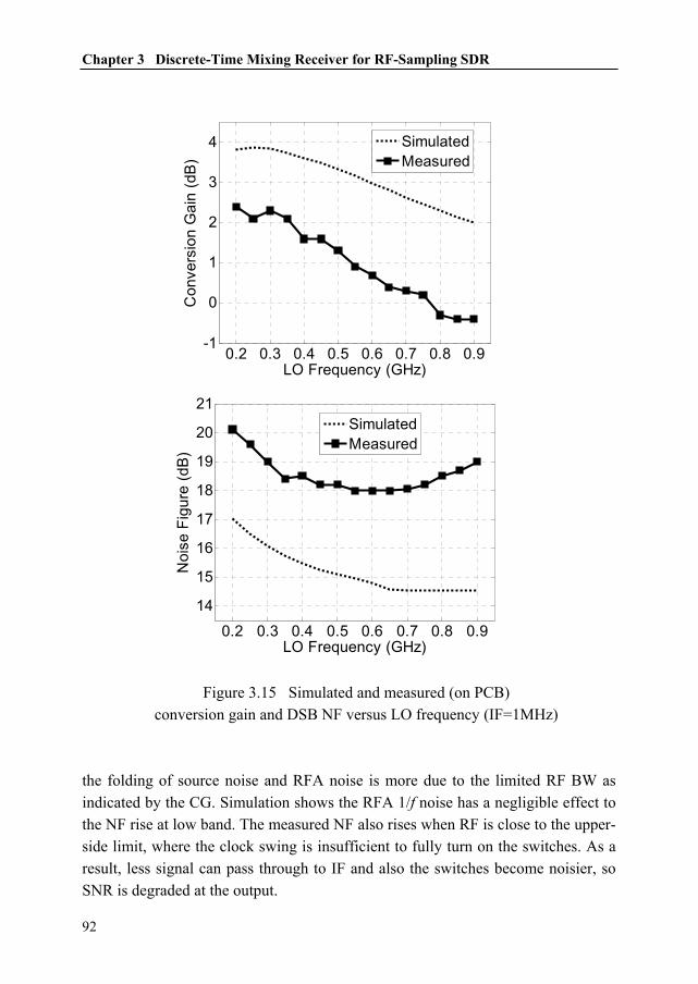
Chapter 3 Discrete-Time Mixing Receiver for RF-Sampling SDR
92
0.2 0.3 0.4 0.5 0.6 0.7 0.8 0.9-1
0
1
2
3
4
LO Frequency (GHz)
Con
vers
ion
Gai
n (d
B)
SimulatedMeasured
0.2 0.3 0.4 0.5 0.6 0.7 0.8 0.9
14
15
16
17
18
19
20
21
LO Frequency (GHz)
Noi
se F
igur
e (d
B)
SimulatedMeasured
Figure 3.15 Simulated and measured (on PCB) conversion gain and DSB NF versus LO frequency (IF=1MHz)
the folding of source noise and RFA noise is more due to the limited RF BW as indicated by the CG. Simulation shows the RFA 1/f noise has a negligible effect to the NF rise at low band. The measured NF also rises when RF is close to the upper-side limit, where the clock swing is insufficient to fully turn on the switches. As a result, less signal can pass through to IF and also the switches become noisier, so SNR is degraded at the output.

3.4 Experimental Results
93
0.2 0.3 0.4 0.5 0.6 0.7 0.8 0.9123456
LO Frequency (GHz)
Con
v. G
ain
(dB)
0.2 0.4 0.6 0.8101214161820
LO Frequency (GHz)
Noi
se F
igur
e (d
B)
Figure 3.16 Measured (on wafer) conversion gain and DSB NF
versus LO frequency (IF=1MHz)
0.2 0.3 0.4 0.5 0.6 0.7 0.8 0.916
17
18
19
20
21
22
23
LO Frequency (GHz)
CG
+NF
(dB)
SimulatedOn PCBOn wafer
Figure 3.17 Normalized output noise (CG+NF) versus LO frequency: comparing simulation and measurements based on PCB and wafer probing

Chapter 3 Discrete-Time Mixing Receiver for RF-Sampling SDR
94
The CG and DSB NF in [1]3 were measured on wafer via probing, which showed a different trend (see Fig. 3.16). It’s very likely due to the different way of installing the off-chip matching resistors. During wafer probing, two 50Ω resistors for input matching were screwed on top of the probe and thus these 50Ω resistors are further away from the chip (~4cm) and this will introduce a transmission-line effect leading to the trend shown in Fig. 3.16, as being verified by simulations. Nevertheless, since the noise from the chip is much larger than the noise from the source as indicated by the large NF, we may compare the normalized output noise (Fig. 3.17), via the sum of CG and NF in dB, which can get rid of the transmission-line effect and indicates mainly the circuit-generated noise at its output. Then three cases, i.e. simulated, measured on PCB and measured on wafer, show a similar trend and their discrepancy is within 1.5dB. Compared to other voltage sampling downconverters, this work shows a superior NF, thanks to the reduced noise folding by employing oversampling and harmonic rejection. Even the measured worst-case NF (20dB) is still 20dB better than [3] and is better than all voltage sampling mixers discussed in [4].
3.4.2 Harmonic Rejection
Fig. 3.18 compares the HR ratio using two different techniques to reject harmonics: DT mixing and conventional FIR filtering [15]. As predicted by theory, the HR ratio of a sampling downconverter using FIR filtering drops significantly over the channel (simulation), while the proposed DT mixing architecture gives wideband HR without channel BW limitation (both simulation and measurement). For DT mixing, the trend of measured results (one typical sample) fits well with the simulated results. However, phase and amplitude mismatches, which are not included in both simulated curves, degrade the HR ratio in measurement. Fig. 3.19 shows the measured HR ratio over the RF band of 10 samples. The worst case 3rd and 5th HR ratios are around 25dB and typically they are between 35dB and 45dB. To investigate whether phase or amplitude error is dominating, we did simulations for three configurations: only amplitude error, only phase error, and both. The results are shown in Fig. 3.20, for 2nd to 6th harmonics of a 0.35GHz LO.
3 The NF shown in [1] should be DSB NF instead of SSB NF.

3.4 Experimental Results
95
.
0 20 40 60 80 10010
20
30
40
50
60
Channel Frequency (MHz)
HR
Rat
io (d
B)
measured DT Mixingsimulated DT Mixingsimulated FIR Filtering
Figure 3.18 Simulated (no mismatch) and measured (a typical sample with mismatch) 3rd-order harmonic-rejection (HR) ratio versus channel frequency
([email protected]) [measured on wafer]
0.2 0.3 0.4 0.5 0.6 0.7 0.8 0.925
35
45
55
LO Frequency (GHz)
3rd
HR
(dB
)
0.2 0.3 0.4 0.5 0.6 0.7 0.8 0.9
25
35
45
55
LO Frequency (GHz)
5th
HR
(dB
)
Figure 3.19 Measured 3rd and 5th HR ratio versus LO frequency (10 samples) [measured on wafer]

Chapter 3 Discrete-Time Mixing Receiver for RF-Sampling SDR
96
1 2 3 4 5 6 730
40
50
60
70
80
Harmonic #
HR
Rat
io (d
B)
gain error onlyphase error onlyphase & gain error
Figure 3.20 Simulated 2nd to 6th HR ratio at 0.35GHz LO (averaged in dB for 10 Monte Carlo runs, mismatch only)
The results indicate that phase error is dominating, which affects not just the 3rd and 5th HR but also the even-order HR. We also did simulations at 0.7GHz LO, and the same conclusion holds. The relatively large phase error is mainly due to many buffer stages used after the divider (Fig. 3.13), leading to large accumulated mismatch. Nevertheless, the HR ratio can be improved via techniques that we will present in Chapter 5, for both amplitude and phase errors, or it can be improved by a tunable front-end LC filter to be presented in Chapter 4.
3.4.3 Performance Summary
Table 3.1 summarizes some of the measured parameters. For the measured in-band linearity, the IIP3 is +10dBm and the IIP2 is +53dBm with two tones around 500MHz. There are three contributions to distortion: the RFA, the MOSFET switches and the IF buffer. The simulated IIP3 of only the SC core is +26dBm and the simulated IIP3 of only the IF buffer is +27dBm. This indicates that the measured IIP3 is dominated by the RFA whose linearity can be degraded by process spread and bondwire inductance of VDD/GND supply pins

3.4 Experimental Results
97
Frequency (GHz) 0.2 to 0.9
Conv. Gain (dB) -0.5 to 2.5DSB NF (dB) 18 to 20
IIP31 +10dBmIIP21 +53dBm
1/f noise corner 250kHz
-3dB IF BW @ 0.7GHz LO
10MHz
VDD 1.2V
DC Current < 16mA
Frequency (GHz) 0.2 to 0.9
Conv. Gain (dB) -0.5 to 2.5DSB NF (dB) 18 to 20
IIP31 +10dBmIIP21 +53dBm
1/f noise corner 250kHz
-3dB IF BW @ 0.7GHz LO
10MHz
VDD 1.2V
DC Current < 16mA
1 Two tones @ 501M & 501.4MHz, LO @ 500MHz Table 3.1 Summary of some measured parameters
[17]4. Since a balun is used in measurement, the IIP3 of each single-ended RFA should be 3dB lower, i.e. +7dBm, which fits the result derived in [17]. Comparing to IIP3 of +11dBm shown in [1] which is based on two-tone test via wafer probing and with around 3dBm adjustment for the transmission-line effect around 500MHz RF, we may conclude that the bondwire in a packaged chip can degrade IIP3 by around 4dB at 500MHz RF. The measured -3dB IF BW is about 10MHz at 0.7GHz LO, while the designed IF BW is 10MHz at 0.5GHz LO. Since the IIR filter BW is determined by both the sampling frequency and the capacitor ratio according to (3.8), the difference is likely due to the variation of the Csu-to-Cb ratio caused by process spread, as they are built by different types of capacitors, i.e. Csu via MOM capacitor and Cb via MOS capacitor. For power consumption, the RFAs draw 2.3mA and the IF test buffers take 2.4mA. The current consumption of the clock is 7.8mA at 200MHz LO and 10.6mA at 900MHz LO. The overall power consumption for all blocks shown in Fig. 3.6 is less than 16mA (19mW) at 1.2V supply.
4 In [17], the discrepancy of IIP3 results based on two-tone test and three-point method is mainly due to the inductance associated with bondwires of supply pins, as being found out later. This effect will be discussed more in Section 4.5.2.

Chapter 3 Discrete-Time Mixing Receiver for RF-Sampling SDR
98
3.5 Conclusions A discrete-time mixing technique was defined via the classification of downconversion techniques in Section 2.2. This chapter elaborates on the receiver architecture based on DT mixing, which has some similar features as CT mixing and solves two problems in traditional RF-sampling receivers: narrowband quadrature demodulation and narrowband harmonic rejection. As a result, the DT-mixing architecture makes RF sampling more suitable to wideband SDR receivers. In this chapter, first we presented the concept of DT mixing, which is a mixing operation in the discrete-time domain. It follows a CT-to-DT sampler to produce the DT input. Simulation shows wideband 90° phase shift for quadrature demodulation without systematic channel bandwidth limitation. Oversampling and harmonic rejection relaxes RF pre-filtering and reduces noise and interference folding. Combining voltage sampling and the DT mixing with HR, the challenges discussed in Section 2.5 can be relieved. Then we showed that the DT-mixing concept can be realized via de-multiplexing. A proof-of-concept DT-mixing downconverter for the 200-to-900MHz RF band employing 8-times oversampling has been built in 65nm CMOS. It can reject the 2nd-to-6th harmonics by 40dB typically without systematic channel bandwidth limitation. Thanks to harmonic rejection which reduces aliasing, the chip also achieves better NF than other state-of-the-art voltage sampling downconverters.
3.6 References [1] Z. Ru, E.A.M. Klumperink, B. Nauta, "A Discrete-Time Mixing Receiver
Architecture with Wideband Harmonic Rejection", IEEE ISSCC, Dig. Techn. Papers, pp.322-616, Feb. 2008
[2] Z. Ru, E.A.M. Klumperink, B. Nauta, “Discrete-Mixing Receiver Architecture for RF-Sampling Software-Defined Radio”, submitted to IEEE J. Solid-State Circuits

3.6 References
99
[3] D. Jakonis, K. Folkesson, J. Dbrowski, et. al., "A 2.4-GHz RF sampling receiver front-end in 0.18-μm CMOS," IEEE J. Solid-State Circuits, vol.40, no.6, pp. 1265-1277, June 2005
[4] H. Pekau and J.W. Haslett, "A 2.4 GHz CMOS sub-sampling mixer with integrated filtering," IEEE J. Solid-State Circuits, vol.40, no.11, pp. 2159-2166, Nov. 2005
[5] R.B. Staszewski, K. Muhammad, D. Leipold, et. al., "All-digital TX frequency synthesizer and discrete-time receiver for Bluetooth radio in 130-nm CMOS," IEEE J. Solid-State Circuits, vol.39, no.12, pp. 2278-2291, Dec. 2004
[6] K. Muhammad, H. Yo-Chuol, T.L. Mayhugh, et. al., "The First Fully Integrated Quad-Band GSM/GPRS Receiver in a 90-nm Digital CMOS Process," IEEE J. Solid-State Circuits, vol.41, no.8, pp.1772-1783, Aug. 2006
[7] R.B. Staszewski, D. Leipold, O. Eliezer, et. al., "A 24mm2 Quad-Band Single-Chip GSM Radio with Transmitter Calibration in 90nm Digital CMOS," IEEE ISSCC, Dig. Tech. Papers, pp.208-607, Feb. 2008
[8] F. Montaudon, R. Mina, S. Le Tual, et. al., "A Scalable 2.4-to-2.7GHz Wi-Fi/WiMAX Discrete-Time Receiver in 65nm CMOS", IEEE ISSCC, Dig. Tech. Papers, pp.362-619, Feb. 2008
[9] R. Bagheri, A. Mirzaei, S. Chehrazi, et. al., "An 800-MHz–6-GHz Software-Defined Wireless Receiver in 90-nm CMOS," IEEE J. Solid-State Circuits, vol.41, no.12, pp.2860-2876, Dec. 2006
[10] V. Giannini, P. Nuzzo, C. Soens, et. al., “A 2mm 0.1G-to-5GHz SDR Receiver in 45nm Digital CMOS”, IEEE ISSCC, Dig. Tech. Papers, pp.408-409, Feb. 2009
[11] The Federal Communications Commission (FCC), “Notice for Proposed Rulemaking (NPRM 03 322): Facilitating Opportunities for Flexible, Efficient, and Reliable Spectrum Use Employing Spectrum Agile Radio Technologies”, ET Docket No. 03 108, Dec. 2003
[12] A. J. Coulson, “A generalization of nonuniform bandpass sampling,” IEEE Trans. Signal Processing, vol. 43, pp. 694–704, Mar. 1995
[13] M. Valkama, M. Renfors, "A novel image rejection architecture for quadrature radio receivers," IEEE Trans. Circuits and Systems II: Express Briefs, vol.51, no.2, pp. 61-68, Feb. 2004
[14] J.A. Weldon, R.S. Narayanaswami, J.C. Rudell, et. al., "A 1.75-GHz highly integrated narrow-band CMOS transmitter with harmonic-rejection mixers," IEEE J. Solid-State Circuits, vol.36, no.12, pp.2003-2015, Dec. 2001

Chapter 3 Discrete-Time Mixing Receiver for RF-Sampling SDR
100
[15] A. Molnar, B. Lu, S. Lanzisera, et. al., "An ultra-low power 900 MHz RF transceiver for wireless sensor networks," IEEE CICC, Proc., pp. 401-404, Oct. 2004
[16] K. Muhammad, R.B. Staszewski, "Direct RF sampling mixer with recursive filtering in charge domain," IEEE ISCAS, Proc, pp. I-577-80 Vol.1, May 2004
[17] Z. Ru, E. Klumperink, C. Saavedra, and B. Nauta, "A tunable 300–800MHz RF-sampling receiver achieving 60dB harmonic rejection and 0.8dB minimum NF in 65nm CMOS," IEEE RFIC Symposium, pp.21-24, June 2009
101
Chapter 4 Filter and Amplifier Techniques for Interference Robustness The previous chapter demonstrated a wideband RF-sampling downconverter based on a discrete-time mixing architecture. However, without LNA, its gain is still low and NF is high, and the achieved harmonic-rejection ratio is also limited due to relatively large phase and amplitude errors. Chapter 4 describes a tunable LC filter and a linearized LNA [1] [2] applied to the DT-mixing downconverter to improve its performance with low extra power consumption and demonstrates a complete RF-sampling receiver. An introduction in Section 4.1 is followed by an overview of the complete RF-sampling receiver in Section 4.2. The description of the tunable LC filter appears in Section 4.3, which can provide “passive” voltage gain and improve the HR ratio flexibly by tuning its center frequency. Then in Section 4.4 the design of the LNA is discussed with a focus on a linearity enhancement technique and the high (non-matched) input impedance. The complete RF-sampling receiver is implemented in 65nm CMOS, with measurement results shown in Section 4.5, demonstrating an NF as low as 0.8dB for a voltage-sampling receiver. Conclusions are drawn in Section 4.6 and references are attached in Section 4.7.
4.1 Introduction Recently, there has been a growing research interest into RF-sampling receivers [3]-[8]. Moving the sampling closer to the antenna can be viewed as an intermediate step in the direction of a software-radio receiver with the full ADC

Chapter 4 Filter and Amplifier Techniques for Interference Robustness
102
close to antenna which targets at greater flexibility. In addition, a direct-RF sampling can offer several other advantages as discussed in Section 2.4.2. For example, sampling exploits switches, capacitors and digital clocks which are compatible with CMOS scaling. Also it is suitable for system-on-chip (SoC) integration since the analog front-end, the ADC and the digital circuits can be clocked synchronously if integer decimation ratios are used between the RF sampling rate and the digital sample rate. To serve software-defined radio (SDR) applications, wideband sampling receivers are desired to cover many RF bands. However, most of the reported RF-sampling receivers are dedicated to narrowband applications such as Bluetooth [5], GSM [6] [8] and WiMax [7]. In fact, compared to mixing, the traditional RF-sampling techniques present some extra challenges when used in wideband applications as described in Section 2.5, such as maintaining quadrature over a wide band and aliasing of wideband noise and interference. Voltage sampling is known to suffer from severe aliasing because all the sampling images have equal magnitude in the ideal case. Charge sampling [5]-[8] yields reduced aliasing and gives similar harmonic downconversion as a mixer due to the SINC function in the frequency domain. The SINC function comes from charge sampling’s (current to charge) integration feature in the time domain, equivalent to convolute with a widowing function [9]. However, charge sampling is not intrinsically suitable to wideband applications since its conversion gain systematically depends on the sampling frequency (see Section 2.5.3). In Chapter 3, a wideband sampling technique, i.e. discrete-time (DT) mixing, has been presented which can deliver constant phase shift over a wide band for frequency-independent quadrature demodulation and wideband harmonic rejection (HR) for reduced aliasing. Thus, the combination of voltage sampling with frequency-independent gain and DT mixing with HR can be suitable to wideband SDR applications. However, the downconverter in Chapter 3 has a few critical performance limitations. Without an LNA, the gain is low (2.5dB) and the NF is high (18dB). Furthermore, the first un-rejected harmonic is the 7th, which may still cause aliasing which results in degraded NF and signal-to-interference ratio. In general, the

4.1 Introduction
103
Figure 4.1 The multi-band RF-sampling receiver number of rejected harmonics is limited by the number of LO phases, and the generation of more LO phases typically requires higher clock frequency, more complexity and more power consumption. Moreover, the HR ratio is severely affected by amplitude and phase accuracy, and the worst-case HR ratio of 25dB (among multiple samples) is not sufficient to handle strong interference in practice. To further reduce the aliasing, in this chapter we apply a front-end tunable LC filter technique which simultaneously provides passive voltage pre-gain1 and harmonic filtering while consuming no power. Pre-gain can improve the NF and the HR at the same time. However, it can degrade the receiver linearity. Therefore we will also present a simple voltage amplifier topology namely an enhanced voltage mirror, applied in the LNA stage, aiming at 3rd-order linearity enhancement. Integrated with the HR downconverter presented in Chapter 3, the complete sampling receiver aims at covering the band of 300MHz to 800MHz (DVB-H band and TV bands for cognitive radio). The receiver can achieve a NF as low as 0.8dB due to the pre-gain, reduced source noise folding, and reduced LNA noise folding. The total HR is also improved from the worst case of 25dB for the basic downconverter to at least 60dB for the complete receiver. In the mean time the 1 We refer to this voltage gain as a passive “pre-gain” meaning that it is achieved before the first active amplification stage, i.e. the LNA.

Chapter 4 Filter and Amplifier Techniques for Interference Robustness
104
receiver achieves a moderate IIP3 of higher than -14dBm. The combination of the LC filter and the LNA can also add more than 20dB gain before downconversion thereby reducing the noise contribution from the later stages. This chapter discusses the design of the sampling receiver with an emphasis on the filter/LNA part while the detail of the downconverter can be found in Chapter 3. 4.2 RF-Sampling Receiver Architecture Fig. 4.1 shows the multi-band zero-IF sampling receiver architecture, in this case for 2 sub-bands. It consists of two LC filters, an LNA, and an RF-sampling downconverter (RFSD) driven by a frequency divider. Two input signal paths are used to cover a 300 to 800MHz bandwidth in two sub-bands, the High Band (HB) and Low Band (LB). These paths can be connected to different antennae as shown, but can also be connected to a single antenna which can cover the full bandwidth. The antennae deliver signals to a pair of LC networks which are followed by the receiver circuit. The inductors are off-chip while the rest of the components are on-chip such as two switchable capacitor banks, an LNA with two selectable single-input differential-output baluns (BL), and an RFSD with 2nd-to-6th order HR driven by a divide-by-4 circuit producing an 8-phase LO. For measurement purposes, after the RFSD, the quadrature baseband outputs are buffered via source followers with a voltage gain of 1. The differential S21 nodes are used to test the transfer function of the LC filter with the balun stage, via an active probe. The RFSD in Fig. 4.1 employs the DT mixing architecture described in Chapter 3. The first stage is an oversampler with an effective sample rate of 8-times the input carrier frequency, i.e. fs=8fc. The second stage contains I/Q DT mixers which down-convert the RF signal to zero-IF with 2nd-to-6th order HR. Oversampling and HR relaxes RF pre-filtering and reduces noise and interference folding. The third stage consists of infinite-impulse response (IIR) low-pass filters, which remove undesired interference and serve as anti-aliasing filters before decimation to a lower sampling rate. The DT mixing architecture can achieve wideband quadrature demodulation and wideband harmonic rejection without systematic channel bandwidth limitations,

4.3 Digitally-Controlled LC Filter
105
and therefore it is more suitable for wideband SDR receivers compared to traditional sampling downconverters. The RFSD was implemented to target at the cognitive radio application recently proposed in the television broadcasting bands [10]. The wideband features of DT mixing can be useful for CR applications which might use non-contiguous segments of free spectrum distributed over a wide band. The dowconverter has a measured gain of -0.5 to 2.5dB, an NF of 18 to 20dB, and an IIP3 of +10dBm. Due to mismatches, the minimum HR ratio is around 25dB. The achieved NF is amongst the best published for voltage sampling downconverters, thanks to the reduced noise folding by employing oversampling and HR. However, the number of rejected harmonics is limited by the number of LO phases and the un-rejected harmonics (7th, 9th etc.) still cause noise aliasing which degrade the NF. For the rejected harmonics (e.g. 2nd to 6th), larger HR ratios are desired to counter strong interference. 4.3 Digitally-Controlled LC Filter To improve the HR ratio and to reduce the noise aliasing, we apply a simple series LC filter structure as the first receiver stage, which can also provide voltage gain to reduce the NF.
4.3.1 Filter Concept
RF pre-filtering is often desired for two main reasons: 1) to attenuate strong out-of-band interferers to a level that can be handled by on-chip electronics; 2) to prevent mixer harmonic images to fold over the wanted signal. It is well-known that a series inductor and a capacitor to ground (Fig. 4.2) define a 2nd-order low-pass filter, with peaking around resonance and attenuation at high frequencies. To suppress the LO harmonics it is sufficient to just use a low-pass filter. In addition, the peaking effect of the filter can be useful to boost the desired signal before an LNA [11] [12]. Here we make the filter tunable by means of switched capacitors (see Fig. 4.3) and apply it to create a flexible sampling receiver with improved noise figure (NF) and harmonic rejection (HR). Next we will derive expressions for the (harmonic) rejection as indicated in Fig. 4.2 and the gain over the tuning range as indicated in Fig. 4.3.

Chapter 4 Filter and Amplifier Techniques for Interference Robustness
106
Figure 4.2 A simple 2nd-order LC filter with transfer function (logarithmic axis)
Assuming the source impedance is Rsrc, the magnitude of the voltage transfer function of the filter in Fig. 4.2 can be derived as
( ) ( ) ( )2
2 4 2 2 2 2 222
1 12 11
out
src srcsrc
VV L C R C LCLC R C ω ωω ω
= =⋅ + ⋅ − +− ⋅ + ⋅
. (4.1)
The peak value of (4.1) over frequency can be found via the derivative of its denominator:
( ) ( )2
3 2 2 2 2/
4 2 2 0src out
src
V VL C R C LCω ω
ω
∂= ⋅ + ⋅ − =
∂. (4.2)
Besides the trivial solution at ω=0, the other solution to (4.2) is 12
02 2 2
2 1 1 / 11 12 2 2
srcp
src
L R C L CL C R QLC
ω ω−
⎛ ⎞−= = ⋅ − ⋅ = ⋅ −⎜ ⎟
⎝ ⎠, (4.3)
where Q is the quality factor of the series RLC network (Q=√(L/C)/Rsrc), and ωp is the peaking frequency and ω0 is the resonance frequency of the LC tank. From (4.3), we can see that ωp lies below ω0, where Q defines how much the difference is between them. Substituting (4.3) into (4.1), the magnitude of the transfer function at ωp can be derived as:
( ) ( )2 22
24 2 2
1 111 1 11 11 44 2
p
out
srcp p src
V QV LC R C
QQ Q Qω ω ω ω=
= = =⎛ ⎞− ⋅ + ⋅ −+ −⎜ ⎟⎝ ⎠
. (4.4)

4.3 Digitally-Controlled LC Filter
107
Based on (4.1) we can see that the gain at the resonance frequency ω0 is exactly Q. For high Q the difference between ω0 and ωp becomes small and the peak gain at ωp is close to Q. Even for a low Q of 2, we still have ωp=0.935ω0 based on (4.3) and |Vout/Vsrc|=1.03Q at ωp based on (4.4), which is only 3% larger than the gain at ω0. Therefore, we may use the gain at ω0 which is easier to define. In Fig. 4.2, at the resonance frequency ω0=1/√(LC), the LC input voltage Vin is equal to 0 since the series LC tank is a short circuit at ω0. Therefore the current flowing into the LC filter is Vsrc/Rsrc, and the voltage magnitude on the capacitor can be written as
0
0
0
1 / 2srcout src src src match
src src src
V L L CV V V Q V Q VR C R Rω ω
ωω=
= ⋅ = ⋅ = ⋅ = ⋅ = ⋅ , (4.5)
where the actual source voltage |Vsrc| is twice as large as the voltage |Vmatch| in case of impedance matching, i.e. Vmatch=Vsrc/2. To benefit from resonant peaking (|Vout|>|Vsrc|) we want Q>1. To get a coarse estimate of the required L and C, we suppose that the desired gain is Gd=Q at ω0, and then find L=Gd⋅Rsrc/ω0 and C=1/(Gd⋅Rsrc·ω0). For Gd=2 and Rsrc=50Ω, at frequencies below 1GHz, this leads to inductors larger than 15nH and capacitors larger than 1.5pF. Clearly, such inductors are not easily realized on chip and even if practical the Q is low. Off-chip inductors can be small, e.g. surface-mounted device (SMD), and with higher Q, and also they are relatively low-cost compared to, for instance, SAW filters. If the receiver has a single-ended RF input, only one external inductor is needed for each sub-band. If Rsrc is defined by the antenna impedance in a radio receiver (usually 50Ω), for a sufficiently high L/C ratio, Q can be larger than 1 and thus this filter can realize “passive” voltage gain around ω0. It can improve the receiver sensitivity, without adding noise and power consumption. This property is favorable compared to SAW filters, which often introduce significant loss. As shown in Fig. 4.2, since inductors conduct DC signal, the attenuation on the low-frequency side is limited. A simple 2nd-order LC filter does not show a characteristic as sharp as most SAW filters, so the suppression of out-of-band interference is less. Whether this is acceptable depends on the application, the antenna characteristic and the linearity of the receiver.
Chapter 4 Filter and Amplifier Techniques for Interference Robustness
108
Figure 4.3 A tunable 2nd-order LC filter with transfer function (logarithmic axis) Such an LC filter does not provide impedance matching, but does give useful voltage pre-gain around the resonance frequency. Moreover, the low-pass transfer function provides significant attenuation for RF signals at multiples of the sampling frequency, hence improving HR. The voltage pre-gain can boost the wanted signal and the improved HR reduces noise and interference aliasing. Both features improve the NF of a wideband sampling receiver. One step further from the filter transfer function, we may quantify the improvement of HR ratio. Via (4.1), the gain for the nth harmonic of the LC resonance frequency can be written as
( ) ( )0
2 2 2 2 222 20 0
1 1( 1) /1
out
src n src
VV n n Qn LC n R Cω ω ω ω= ⋅
= =− +− ⋅ ⋅ + ⋅ ⋅
. (4.6)
Since the gain at the fundamental harmonic (n=1), i.e. ω0, is equal to Q according to (4.6). For the nth harmonic (n=2, 3, 4…), we can achieve a HR improvement of
( )2 2 2 2 210 10 220log ( 1) / 20log ( 1) (if >> )
-1⎡ ⎤= ⋅ − + ≈ ⋅ −⎣ ⎦n
nHR Q n n Q Q n Qn
. (4.7)
Even for a low Q of 2, we can still get HR3=24dB and HR5=34dB. Please note that both the resonant peaking (Q) and the filter’s 2nd-order roll-off contribute to the HR ratio, as indicated in Fig. 4.2. The filter in Fig. 4.2 is dedicated to one resonance frequency. To cover a wider frequency range, we would like to have a tunable ω0. In theory, an arbitrary bandpass characteristic can be made by a combination of inductors and capacitors. For a high-order filter, tuning to another frequency, while maintaining the bandpass shape involves tuning all or at least many of its components. Hence, for simplicity

4.3 Digitally-Controlled LC Filter
109
of implementation it seems prudent to stick to low-order tunable filters. As inductors are not easily tunable and varactors often introduce nonlinearity, we aim to exploit MOS-switches and linear metal capacitors for tuning, which can be digitally controlled, as shown in Fig. 4.3. Switching the capacitor to tune the filter to another frequency also changes its gain, but this gain variation can be acceptable. If we keep the frequency tuning range2 smaller than 40%, i.e. ω0,max/ω0,min<1.5, the gain variation can be less than 3dB. The gain variation depends on the fact that the tuning is achieved whether via switching inductors or capacitors. Based on (4.5), we can derive that if purely switching the capacitor, i.e. fix the inductor, the gain variation is
0,
0,
.aa b
b b a
G CG C
ωω
= = (4.8)
That means the gain is proportional to the resonance frequency. Yet, by switching the inductor and fixing the capacitor, the gain variation is
0,
0,
ba a
b a b
G LG L
ωω
= = . (4.9)
That means the gain is inversely proportional to the resonance frequency in case of switching inductors to tune the working band (Section 4.3.2).
4.3.2 Implementation
Fig. 4.1 shows the schematic of the implemented LC filter. Two on-board SMD inductors, 36nH for high-band (HB) and 100nH for low-band (LB), with two metal-oxide-metal (MOM) capacitors (C1=1.2pF, C2=0.5pF) for each inductor, are included to demonstrate the multi-band function. Which signal path in use is determined by enabling one of the balun-LNAs by setting K0 to be 0 or 1. The band selection is achieved in two steps, a coarse selection and a fine tuning. The coarse
2 The tuning range is defined as the ratio of the absolute tuning bandwidth to the middle frequency of the tuning band, i.e. 2(ω0,max-ω0,min)/(ω0,max+ω0,min).
Chapter 4 Filter and Amplifier Techniques for Interference Robustness
110
K1K2 Cfix(pF)
Ctune(pF)
Ctot(pF)
00 0.69 0.36+0.24 1.29
01 0.69 0.36+0.5 1.55
10 0.69 1.2+0.24 2.13
11 0.69 1.2+0.5 2.39
K1K2 Cfix(pF)
Ctune(pF)
Ctot(pF)
00 0.69 0.36+0.24 1.29
01 0.69 0.36+0.5 1.55
10 0.69 1.2+0.24 2.13
11 0.69 1.2+0.5 2.39
Cfix=CLNA+Cpad+Ctp+CPCB=0.17+0.1+0.17+0.25=0.69pF
Figure 4.4 Sources of parasitic capacitance in the LC filter selection is inherent in the LNA stage (K0) which can be powered on/off to select which filter bank in use. The fine tuning is achieved by varying the capacitor values of the LC tank via digital bits (K1, K2). Via the combination of selecting inductors and capacitors, we can set eight resonance frequency points (f0) of the filter, i.e. controlling via three bits “K0K1K2”. These resonance frequencies are discrete points but the filter can continuously cover a large bandwidth by operating over a small bandwidth around each f0 (Fig. 4.3). However, the resonance frequency and the Q are heavily affected by the parasitic capacitance, as modeled in Fig. 4.4. The model includes the input capacitance of LNA CLNA, the pad capacitance Cpad, the PCB capacitance CPCB. Ctp indicates the top-plate parasitic capacitance of C1 and C2 together. Cbp1 and Cbp2 indicate the bottom-plate parasitics of C1 and C2 respectively, as well as the parasitics of their switches.
4.3 Digitally-Controlled LC Filter
111
K0K1K2 Total L(nH)
Total C(pF)
f0(MHz)
Q a) Gain=2Q(dB)
3rd|5th Harmonic Rejection (dB)
HB000 36 1.29 740 3.3 16 28 38
001 36 1.55 670 3.0 16 27 37010 36 2.13 570 2.6 14 26 36011 36 2.39 540 2.5 14 26 35
LB100 100 1.29 440 5.6 21 33 43101 100 1.55 400 5.1 20 32 42110 100 2.13 340 4.3 19 31 40111 100 2.39 320 4.1 18 30 40
a) Refer to a 50Ω real impedance.
Table 4.1 Calculated parameters of the implemented LC filter (Figure 4.1) The parasitics of C1 and C2 are about 10% of their nominal values and the parasitics of switches are about 0.4pF due to large switches used for low on-resistance (1Ω). Via simulation and estimation, we get CLNA=0.17pF, Cpad=0.1pF, Ctp=0.17pF, Cbp1=0.52pF, and Cbp2=0.45pF; CPCB is about 0.25pF (fitted after experiments). The table in Fig. 4.4 summarizes the total capacitance Ctot in each configuration of K1K2. Table 4.1 lists the resonance frequency, the Q, and the HR ratio for each of the filter 3-bit settings (K0K1K2), calculated via (4.5) and (4.7)-(4.9). Please note that the voltage gain here is equal to 2Q, referred to Vmatch in (4.5). The lowest Q in the whole band is 2.5, for K0K1K2=011. The bondwire of 1.5nH and the switch-on resistance of 1Ω have a negligible effect to the filter performance. Also the quality factors of the on-board inductors are in the order of 30 to 40, which also can hardly affect the filter performance. The calculated parameters in Table 4.1 have been verified by simulations. At resonance, the LC filter input impedance is 0 (short) instead of Rsrc. Receivers without input matching have been proposed before, e.g. in [12]-[14]. Although this may complicate RF pre-filter design and may introduce issues with respect to reflections, it also has advantages. Note that for input matching there is a maximum

Chapter 4 Filter and Amplifier Techniques for Interference Robustness
112
power transfer, but it degrades the voltage by half, i.e. Vmatch=Vsrc/2 as shown in (4.5). For voltage sensing devices such as a MOSFET at f<<fT, the maximum voltage transfer is more of interest, and an unmatched input may have advantages, e.g. lower NF, lower power consumption, and higher Q (no extra resistance from the matching device). The inductors are placed very close to the chip, and 50Ω transmission lines are used to connect the inductors to the antennae. If there is no impedance mismatch between the antenna and its connection lines, the voltage amplitude sensed by the LNA input is still well defined by (4.5), independent of the line length [13]. Moreover, since here we deal with frequencies below 1GHz, it is often possible to use PCB lines between the antenna and the chip which are much shorter than the wavelength. In that case, the transmission line effect can be made negligible. The reflection due to the impedance mismatch at the input of the LC filter will create standing waves on the transmission line. If the transmission line has a negligible length or is well matched with antenna, the antenna will absorb the reflected wave and radiate it back into the air. But this reflection should not violate the radio regulation, since any obstacle in surroundings may cause the same consequence. According to (4.5), the gain is well defined if the source impedance is well defined. However, antenna impedance is not purely resistive but involves re-active parts such as inductance and capacitance. Nevertheless, for a well-designed antenna, its impedance in the desired band can be approximated as purely resistive while the re-active parts resonate in that band. The resonant effect of the antenna can provide attenuation of interference and hence further improve the HR ratio. In practice, the antenna impedance can also vary with the environment, e.g. due to the reflection of electromagnetic waves by surroundings. If an antenna is aimed at achieving S11<-10dB referred to a 50Ω source, the real part of the antenna impedance varies in the range of 25Ω to 100Ω. This variation represents a change of Q by 0.5 to 2 times from the nominal 50Ω case. According to (4.5), the pre-gain variation is directly proportional to the Q variation. However, for NF the variation is less because the antenna noise voltage also

4.4 Amplifier based on Enhanced Voltage Mirror
113
changes when its impedance varies. This effect can be seen from the overall noise at the output of the LC filter:
22, / /4 4n afterLC
srcsrc src
v L C L CkTR kTf R R
⎛ ⎞= ⋅ = ⋅⎜ ⎟⎜ ⎟Δ ⎝ ⎠
. (4.10)
If the antenna impedance changes by a factor of 2, the gain changes by 6dB and the NF changes by 3dB in the worst case. It happens when the antenna noise is much smaller than the noise from the receiver (the LNA and the downconverter). Generally, the NF variation should be less than 3dB, depending on how much the antenna noise is boosted by the passive pre-gain. If the antenna noise is dominating due to a high passive pre-gain, then the NF variation can be negligible. In case that the variation is not acceptable, additional measures might be taken to adaptively transform the antenna impedance. Anyhow, the variation of antenna impedance can also be problematic in a receiver with input impedance matching. 4.4 Amplifier based on Enhanced Voltage Mirror Since the presented LC filter provides pre-gain before the LNA stage, the required linearity of the LNA is hence raised. Now we will propose a simple amplifier topology to construct a balun-LNA, which can provide IIP3 enhancement.
4.4.1 LNA Topology
As shown in Fig. 4.5, the balun-LNA is constructed using inverters as transconductors. Compared to common-source amplifiers with a single NMOS or PMOS as the transconductor, they can provide a large gm/Id ratio as the bias current of the PMOS is re-used by the NMOS, while also tolerating large voltage swings which is advantageous for handling large interference. In fact, all inverters in Fig. 4.5 are self-biased via feedback resistors, so that no extra bias circuitry is needed. Fig. 4.6 shows the schematic of a unit amplifier used in the LNA where gm=gm,N+gm,P, It includes both the feedback resistor (Rbig) for the driving inverter and the feedback resistor (Rfb) for the loading inverter. The absolute value of Rbig is not critical but is large enough (1MΩ) only for DC biasing

Chapter 4 Filter and Amplifier Techniques for Interference Robustness
114
Figure 4.5 Implemented LC filter and LNA
Figure 4.6 Schematic of a unit amplifier used in the LNA
purpose without affecting the transconductance function. Therefore in Fig. 4.5, Rbig of all driving inverters are not shown for figure clarity. To understand the basic functionality of the LNA in Fig. 4.5, let’s first consider all feedback resistors of the loading inverters as shorts, realizing an impedance of 1/gm or 1/(2gm) where gm is the unit transconductance in use. Driven by a transconductance of 2gm, an inverting gain is realized. The gain is -2 in all cases

4.4 Amplifier based on Enhanced Voltage Mirror
115
Figure 4.7 Model for the unit amplifier
except for the “inverting stage” whose gain is -1. Thus the 1st stage realizes a balun function with a 6dB gain from the input to each of the differential outputs (the single-to-differential gain is 4), and the 2nd stage is a pseudo-differential amplifier with another 6dB gain. As can be seen from Fig. 4.5, the loading inverters have their inputs and outputs connected via a feedback resistor, either R or 2R, for the purpose of nonlinearity compensation (Section 4.4.2). The feedback resistors and the output impedance of the inverters can affect the amplifier behavior. To analyze the gain and noise performance, we model the unit amplifier (Fig. 4.6) as Fig. 4.7, including the output resistance of the driving inverter (rdsD) and the loading inverter (rdsL) and the feedback resistor Rfb. The equivalent input impedance of the loading inverter can be written as
1 (if >>1 and >> )1
+= ≈ ⋅
+ ⋅fb dsL
L mL dsL dsL fbmL dsL mL
R rZ g r r R
g r g. (4.11)
In our design, gmL=10mS, rdsL=1.5kΩ, and Rfb=2/gmL=200Ω and therefore the approximation in (4.11) holds. Then the voltage gain can be written as
(if >>1)1
⋅= ⋅ ≈ ⋅ ≈ ⋅
+ + ⋅o dsD L dsD mD
mD mD mL dsDin dsD L dsD mL mL
v r Z r gg g g rv r Z r g g
. (4.12)
Traditional common-source amplifiers often rely on the product of transistor gm and load resistance to define the gain, which can vary a lot due to process spread. The amplifier topology presented here defines its gain via the ratio between transistors’ gm, which is less sensitive to process spread especially when gain ratios via unit transconductors are used.
Chapter 4 Filter and Amplifier Techniques for Interference Robustness
116
To gain some insight into the noise behavior of the circuit, one can idealize the transconductor output resistors, by making rdsD and rdsL infinite in the noise analysis. There are three noise contributors: gmD, gmL and Rfb. Ignoring rdsD and rdsL, the noise current of gmD (inD
2/Δf = 4kTγ·gmD) can only flow through Rfb. As a result, a noise voltage (vnD) appears at node X which generates a current via gmL to match inD. The noise voltage can be written as vnD = inD·ZL ≈ inD/gmL. Another noise voltage (vnL) also appears at node X to generate a current via gmL to cancel its own noise current (inL
2/Δf = 4kTγ·gmL), which can be written as vnL = inL/gmL. However, as Rfb is in series with a current source which models the noise current of gmD, it does not affect the noise voltage at node X. Therefore, for a unit amplifier, the noise voltage at node X can be derived as:
2 2 2
2
4 4n nD nL mD
mL mL
v v v kT g kTf f f g g
γ γ⋅= + = +
Δ Δ Δ. (4.13)
Now consider the NF of the complete LNA shown in Fig. 4.5., According to (4.5), the voltage gain (referred to Vsrc) of the LC filter is Q, therefore the source noise voltage at the input of the LNA is 4kTRsrc·Q2. Applying (4.13), we can derive the total noise voltage at the LNA output as:
2, 2 2 2 2
SourceLNA 1st-Stage Inverting Stage
(Exclude Inverting Stage)
LNA 2nd-Stage
4 2 4 4 44 8 4 22 2
4 2 4 2
n LNAosrc
m m m m
m m
v kT kT kT kTkTR Qf g g g g
kT kTg g
γ γ γ γ
γ γ
⎛ ⎞ ⎛ ⎞⋅= ⋅ ⋅ + + ⋅ + + ⋅⎜ ⎟ ⎜ ⎟Δ ⎝ ⎠ ⎝ ⎠
⎛ ⎞⋅+ + ⋅⎜ ⎟⎝ ⎠
144244314444244443 144424443
1 2
2 584 64 4srcm
kTR Q kTg
γ= ⋅ + ⋅444 4443
. (4.14)
Given Rsrc=50Ω and gm=10mS, the NF of the LC-LNA combination is
2,
2 2 2 2
58 / 58 /10 1.81 1 14 64 64 50 64
γ γ γ−
⋅ ⋅= = + = + = +
⋅ ⋅ Ω ⋅n LNAo m
LC LNAsrc src
v g mSNFkTR Q R Q Q Q
. (4.15)
We can see that this NF will be improved by the LC filter pre-gain defined by the Q. If Q=2 and assuming γ=1, then NF=1.6dB. In Fig. 4.5, due to the additional stage used for inverting (marked in box) in the Vo- path, an extra delay exists therefore the balun performance can degrade at a higher frequency. Any capacitive load at node A (Fig. 4.5) affects both differential paths,

4.4 Amplifier based on Enhanced Voltage Mirror
117
Rfb
gmgmvin vo
io
va
ia
Figure 4.8 IM3 compensation mechanism in a unit amplifier
which doesn’t produce imbalance. Loading at node B only affects the Vo- path and thus should be minimized. Nevertheless the extra delay on the Vo- path can be compensated by adding a capacitor with an appropriate value at the Vo+ node to better balance the two paths. However, it was not included in this design.
4.4.2 Mechanism of Nonlinearity Compensation
The passive pre-gain induced by the LC filter improves receiver NF, but it can also degrade linearity. The aim of the feedback resistors in the loading inverters (Fig. 4.5 to Fig. 4.7) is to mitigate this effect by compensating the 3rd-order distortion. To understand the compensation principle, consider first the simple case with two equally-sized inverters for a voltage gain of -1 (Fig. 4.8), and only include the linear term and the 3rd-order term in the V-I conversion. If one models the transconductor as a nonlinear V-I converter with no vds dependence, then only gm1 and gm3 terms need to be considered:
31 3
31 3
( )
( )o m in m in in
a m o m o o
i g v g v f v
i g v g v f v
⎧ = + =⎪⎨− = + =⎪⎩
. (4.16)
Assuming negligible gate-current, io and ia are equal due to Kirchhoff’s Current Law (KCL), and the solution for (4.16) is vo=(-1)·vin which is a perfectly linear V-V transfer function. This is because we assume the i(v) function of the driving and loading inverters are equal, i.e. vo(ia) is an inverse function of io(vin). According to (4.16), io=f(vin) and ia=-f(vo), then we have:
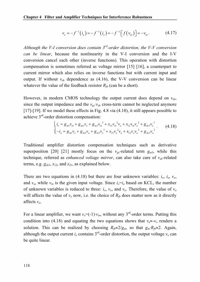
Chapter 4 Filter and Amplifier Techniques for Interference Robustness
118
( ) ( ) ( )1 1 1o a o in inv f i f i f f v v− − − ⎡ ⎤= − = − = − = −⎣ ⎦ . (4.17)
Although the V-I conversion does contain 3rd-order distortion, the V-V conversion can be linear, because the nonlinearity in the V-I conversion and the I-V conversion cancel each other (inverse functions). This operation with distortion compensation is sometimes referred as voltage mirror [15] [16], a counterpart to current mirror which also relies on inverse functions but with current input and output. If without vds dependence as (4.16), the V-V conversion can be linear whatever the value of the feedback resistor Rfb (can be a short). However, in modern CMOS technology the output current does depend on vds, since the output impedance and the vgs·vds cross-term cannot be neglected anymore [17]-[19]. If we model these effects in Fig. 4.8 via (4.18), it still appears possible to achieve 3rd-order distortion compensation:
3 2 2 31 1 3 21 12 3
3 2 2 31 1 3 21 12 3
o m in ds o m in in o in o ds o
a m o ds a m o o a o a ds a
i g v g v g v x v v x v v g v
i g v g v g v x v v x v v g v
⎧ = + + + + +⎪⎨− = + + + + +⎪⎩
. (4.18)
Traditional amplifier distortion compensation techniques such as derivative superposition [20] [21] mostly focus on the vgs-related term gm3, while this technique, referred as enhanced voltage mirror, can also take care of vds-related terms, e.g. gds3, x12, and x21, as explained below. There are two equations in (4.18) but there are four unknown variables: io, ia, vo, and va, while vin is the given input voltage. Since io=ia based on KCL, the number of unknown variables is reduced to three: io, vo, and va. Therefore, the value of va will affects the value of vo now, i.e. the choice of Rfb does matter now as it directly affects va. For a linear amplifier, we want vo=(-1)·vin, without any 3rd-order terms. Putting this condition into (4.18) and equating the two equations shows that va≈-vo renders a solution. This can be realized by choosing Rfb≈2/gm, so that gm·Rfb≈2. Again, although the output current io contains 3rd-order distortion, the output voltage vo can be quite linear.

4.4 Amplifier based on Enhanced Voltage Mirror
119
gm·R
IIP3
(dB
m) @
vo
R
2gm2gmvin vo va
gain=-1
gm2gmvin vo va
gain=-2 2R
0 0.5 1 1.5 205
1015202530
gain=-1gain=-2
Figure 4.9 Simulated IIP3 versus gm·R of two unit amplifiers (gain=-1, gain=-2) with two tones around 500MHz
The above analysis is only valid to the first order. Since vo is linear with vin and ia is nonlinear with vo, va=vo+ia·Rfb cannot be linear with vin. Therefore va is only equal to -vo to the first order, and then to satisfy io=ia, vo must also be polluted by some distortion, but to a much lower degree than va, as illustrated by the two-tone-test spectra in Fig. 4.8. This is why in Fig. 4.5 all the nodes corresponding to va are not used. Please note that, for va≈-vo, the feedback resistor for gm should be 2R and for 2gm it should be R if gm·R=1, as shown in Fig. 4.5. This technique also works for non-equal inverters but the linearity improvement will be less. Here we also use it for the stages with a gain of -2. The simulation results presented in Fig. 4.9 shows that a peak IIP3 exists at R≈1/gm for both gain of -1 and -2 cases. A 25% change of gm·R from 1 can still give about 5dB better IIP3 compared to gm·R=0 (a short as feedback). This principle is useful for the odd-order distortion but not very effective for the even-order distortion. Nevertheless, by using an inverter, the even-order distortion of the NMOS and PMOS can compensate each other nominally [22], although process spread may lead to residual distortion. A differential configuration can also

Chapter 4 Filter and Amplifier Techniques for Interference Robustness
120
Figure 4.10 Micrograph of the chip implemented in 65nm CMOS
Figure 4.11 SMD inductors (36nH and 100nH) on PCB
help with even-order distortion after the balun. Moreover, the AC coupling capacitor used between the LNA and the RFSD can block the low-frequency IM2 components generated by the LNA.
4.5 Experimental Results

4.5 Experimental Results
121
10-1 100-40
-30
-20
-10
0
10
20
30
f (GHz)H
igh-
Band
S21
(dB)
10-1 100-40
-30
-20
-10
0
10
20
30
f (GHz)
Low
-Ban
d S2
1 (d
B)
Figure 4.12 Measured S21: LC Filter plus LNA 1st-stage (Passive: LC pre-gain; Active: LNA 1st-stage gain)
A proof-of-concept receiver was implemented in 65nm CMOS and the chip micrograph is shown in Fig. 4.10, taking an active area=0.5mm2. The chip is packaged in a 32-pin Heat-sink Very-thin Quad Flat-pack No-leads (HVQFN) package and measured on PCB and the input port has Rsrc=50Ohm for all tests. Two inductors of value 100nH and 36nH are mounted on board, close to the chip package (Fig. 4.11). With a 1.2V supply, the current consumption is 5mA for the LNA, 10mA for the clock at 800MHz LO, and 2.4mA for the output buffer, while the RFSD consumes no power since it only contains switches and capacitors.
4.5.1 Filter Response, Gain, NF, and HR
To verify the tunability of the digitally-controlled LC filter, we measured S21 of the LC filter together with the 1st stage of the LNA (Fig. 4.1 & Fig. 4.5). The input of the LC filter is connected to a Vector Network Analyzer via PCB traces and co-axial cables. At the output of the LNA 1st stage, an active probe (up to 3GHz) is used to connect the S21 node (see Fig. 4.1) to the Vector Network Analyzer. The active probe performs the differential to single-ended conversion with 1x voltage gain as well as the impedance transformation to 50Ω desired for measurements.

Chapter 4 Filter and Amplifier Techniques for Interference Robustness
122
0.3 0.4 0.5 0.6 0.7 0.8
60
80
100
120
f (GHz)
HR
ratio
(dB)
HR3HR5
Figure 4.13 Measured 3rd and 5th order HR ratio over the RF band (4 chips) Fig. 4.12 shows the measured S21 for low-band (LB) and high-band (HB) respectively, which can continuously cover 300-500MHz and 500-800MHz with less than 3dB gain variation in each band. Please note that the gain indicated here is a voltage gain referred to Vmatch in (4.5). Due to different inductor values (36nH and 100nH) used, the Q and therefore the peak gain and bandwidth are different for LB and HB. Considering the 11dB gain from LNA 1st stage (verified by measurement), the “passive” LC pre-gain is about 16dB for LB and 11dB for HB. Comparing Fig. 4.12 and Table 4.1, we can see that the measured resonance frequencies fit the calculated ones well, via a 0.25pF excess capacitance from PCB (CPCB in Fig. 4.4), e.g. due to the leadframe and the soldering pad. However, the measured gains (passive) are about 5dB lower than the calculated (and simulated) gains listed in Table 4.1. A possible reason is the deviation from 50Ω of the characteristic impedance of the connection cables and the PCB traces. Therefore the 50Ω source impedance is transformed to a higher value. Both bands show an effective suppression of LO harmonics. The measured LB HR ratios from LC filter fit what calculated in Table 4.1, but the measured HB HR ratios are at least 7dB higher than the calculated values. We attribute this difference to the gain roll off at relatively high frequencies due to circuit parasitics of the LNA 1st stage and the sharp notch in the HB transfer function due to the inductor self-resonance. The measured 3rd and 5th HR of the complete receiver (4 chips) is shown in Fig. 4.13, where the HR ratios for the whole band are above 60dB, with roughly 30dB contribution from the LC filter and the other 30dB from the RFSD.

4.5 Experimental Results
123
0.3 0.4 0.5 0.6 0.7 0.80
1
2
3
4
5
f (GHz)
NF
(dB
)
0.3 0.4 0.5 0.6 0.7 0.820
22
24
26
28
30
f (GHz)
Gai
n (d
B)
Figure 4.14 Measured gain and NF of the complete receiver over the RF band
0.3 0.4 0.5 0.6 0.7 0.835
40
45
50
55
f (GHz)
IIP2
(dB
m)
0.3 0.4 0.5 0.6 0.7 0.8
-14
-12
-10
-8
f (GHz)
IIP3
(dB
m)
Figure 4.15 Measured IIP3 and IIP2 of the complete receiver over the RF band
Theoretically, a balanced LO with 50% duty cycle can reject all even-order harmonics. However, experiments show the 2nd-order HR can become the bottleneck, since the LC filter suppresses the 3rd and higher order harmonics more. This requires balanced LO being more accurate. Fig. 4.14 plots the measured voltage gain and NF of the complete receiver, at the peak frequencies of both bands. The gain difference from LB to HB matches the measured S21 in Fig. 4.12. The NF is measured via the Y-factor method to read the noise voltage at the output. Fig. 4.14 shows a clear link between gain and NF, i.e. the high “passive” gain at LB also gives a better NF. The measured minimum NF is

Chapter 4 Filter and Amplifier Techniques for Interference Robustness
124
gm·R↓
1.1 1.15 1.2 1.25 1.3-6
-4
-2
0
2
4VDD=1.2V
VDD (V)
Figure 4.16 Measured LNA IIP3 at different VDD levels
with two tones around 445MHz
0.8dB for the complete receiver, which shows a very low NF can be achieved with low power consumption (6mW for the LNA and downconverter), even for the voltage sampling receiver that suffers from severe noise folding. Such a low NF is achieved via a combination of sufficient “passive” pre-gain to boost the desired signal, 2nd-order LC filter to prevent the source noise folding, and HR downconverter to prevent the source and the LNA noise folding.
4.5.2 Linearity
The measured in-band IIP3 and IIP2 via two-tone test are shown in Fig. 4.15. Since the LNA is AC coupled to the RFSD (Fig. 4.1), the IIP2 is dominated by RFSD and degrades with higher frequency (worst case: +38dBm), rather independent of the gain. Most likely it is due to the degraded balun performance at the high band, since IIP2 directly relates to the matching of differential signal.
From the IIP3 plot, we see the direct effect of the “passive” pre-gain, sharing almost the same trend as NF. The worst-case IIP3 of -14dBm is moderate for a complete receiver, especially considering that this IIP3 corresponds to a very low NF of 0.8dB.

4.5 Experimental Results
125
0 0.5 1 1.5 2-6-4-2024
Figure 4.17 LNA IIP3: measurement versus simulation Considering the LC pre-gain, the LNA plus RFSD combination should present an IIP3 around +2dBm. Simulation shows the LNA dominates IIP3, which means the 2-stage LNA has an IIP3 around +2dBm. To verify the effect of gm·R to the IIP3, we measured and derived the IIP3 of the 2-stage LNA (Fig. 4.16) at different VDD levels, which affects the gm value. Clearly we can see the trend of IM3 compensation which verifies the theory. Considering VDD=1.2V, however, referred to the input of the LNA 2nd stage (S21 nodes in Fig. 4.5), the IIP3 should be about +7dBm, since the LNA 1st stage has a single-ended gain of 5dB. This IIP3 is far from optimum as simulated in Fig. 4.9, for the gain=-2 curve, corresponding to a 50% variation of gm·R from 1. One reason is the process spread which makes the gm·R value different from the designed 1. On the other hand, the measured DC linearity via a three-point method [23] is at least 4dB better than the two-tone test result. This gap of 4dB could mainly be due to the supply bondwire inductance which is not considered in the simulation of Fig. 4.9. Measurement via wafer probing (instead of packaged chips on PCB) can exclude the bondwire effect and indeed shows 4dB better IIP3 (see Section 3.4.3). The bondwire inductance disturbs the compensation mechanism since the driving inverter and the loading inverter will share the same bondwire but with different inverter sizes for the gain=-2 case (Fig. 4.9). Simulation has been carried out to include non-ideal effects from both process spread (slow-NMOS and slow-PMOS indicated by measured DC operating point)

Chapter 4 Filter and Amplifier Techniques for Interference Robustness
126
and supply bondwire inductance (VDD: 2nH, GND: 0.5nH, as estimated from the chip size and the specific package used). Fig. 4.17 compares the measured IIP3 and the simulated IIP3 around 500MHz RF at VDD=1.2V. The simulation agrees with the measured trend of Fig. 4.16 and it also indicates that the IIP3 improvement is about 4dB via the enhanced voltage mirror by applying Rfb (instead of a short) in the loading inverter (Fig. 4.6). Both Fig. 4.16 and Fig. 4.17 indicate that the distortion compensation is still effective, although additional techniques are desired to improve its robustness against process spread and bondwire inductance. For instance, techniques to change gm to track an R or C value are well-known for filters. 4.6 Conclusions A 300-to-800MHz multi-band RF-sampling receiver is presented, with 0.8dB minimum NF and more than 60dB HR. It is based on a discrete-time mixing harmonic-rejection downconverter in 65nm CMOS, preceded by a voltage sensing LNA which exploits a simple 2nd-order LC filter with one external inductor per sub-band. This LC filter does not provide impedance matching but does provide voltage pre-gain and also acts as a harmonic filter tunable via on-chip switchable capacitor banks which can be controlled by digital codes. The filtering significantly improves the sampling downconverter’s HR ratio from 25dB to more than 60dB for 3rd and 5th harmonics, resulting in less interference aliasing. The voltage-sensing balun-LNA is built via a simple amplifier topology consisting of inverters and resistors. It reduces the 3rd-order nonlinearity due to both vgs and vds related terms, via an enhanced voltage mirror technique. The compensation effect is demonstrated via measurements, although an improved robustness against process spread and supply bondwire inductance is desired. A low NF (0.8dB) at a low power consumption (6mW for the LNA and downconverter) for a voltage sampling receiver can be achieved by a sufficient “passive” pre-gain from the LC filter, together with the reduced noise aliasing thanks to both the LC filter and the harmonic-rejection downconverter.

4.7 References
127
4.7 References [1] Z. Ru, E. Klumperink, C. Saavedra, B. Nauta, "A tunable 300–800MHz RF-
sampling receiver achieving 60dB harmonic rejection and 0.8dB minimum NF in 65nm CMOS," IEEE RFIC Symposium, pp.21-24, June 2009
[2] Z. Ru, E.A.M. Klumperink, C.E. Saavedra, B. Nauta, "A 300-800MHz Tunable Filter and Linearized LNA applied in a Low-Noise Harmonic-Rejection RF-Sampling Receiver", submitted to IEEE J. Solid-State Circuits, Special Issue on RFIC Symposium 2009
[3] D. Jakonis, K. Folkesson, J. Dbrowski, et. al., "A 2.4-GHz RF sampling receiver front-end in 0.18-μm CMOS," IEEE J. Solid-State Circuits, vol.40, no.6, pp. 1265-1277, June 2005
[4] H. Pekau and J.W. Haslett, "A 2.4 GHz CMOS sub-sampling mixer with integrated filtering," IEEE J. Solid-State Circuits, vol.40, no.11, pp. 2159-2166, Nov. 2005
[5] R.B. Staszewski, K. Muhammad, D. Leipold, et. al., "All-digital TX frequency synthesizer and discrete-time receiver for Bluetooth radio in 130-nm CMOS," IEEE J. Solid-State Circuits, vol.39, no.12, pp. 2278-2291, Dec. 2004
[6] K. Muhammad, H. Yo-Chuol, T.L. Mayhugh, et. al., "The First Fully Integrated Quad-Band GSM/GPRS Receiver in a 90-nm Digital CMOS Process," IEEE J. Solid-State Circuits, vol.41, no.8, pp.1772-1783, Aug. 2006
[7] F. Montaudon, R. Mina, S. Le Tual, et. al., "A Scalable 2.4-to-2.7GHz Wi-Fi/WiMAX Discrete-Time Receiver in 65nm CMOS," IEEE ISSCC, Dig. Tech. Papers, pp.362-619, 3-7 Feb. 2008
[8] R.B. Staszewski, D. Leipold, O. Eliezer, et. al., "A 24mm2 Quad-Band Single-Chip GSM Radio with Transmitter Calibration in 90nm Digital CMOS," IEEE ISSCC, Dig. Tech. Papers, pp.208-607, 3-7 Feb. 2008
[9] G. Xu, J. Yuan, “Performance analysis of general charge sampling”, IEEE Trans. Circuits and Systems II: Express Briefs, vol. 52, no. 2, Feb. 2005
[10] The Federal Communications Commission (FCC), “Notice for Proposed Rulemaking (NPRM 03 322): Facilitating Opportunities for Flexible, Efficient, and Reliable Spectrum Use Employing Spectrum Agile Radio Technologies”, ET Docket No. 03 108, Dec 2003
[11] W. Sansen, “Analog Design Essentials”, Springer, 2006 [12] M. Steyaert, et. al, “A Single-Chip CMOS Transceiver for DCS-1800
Wireless Communications”, IEEE ISSCC, Dig. Tech. Papers, Feb. 1998

Chapter 4 Filter and Amplifier Techniques for Interference Robustness
128
[13] M. Camus, et. al., “A 5.4mW 0.07mm2 2.4GHz Front-End Receiver in 90nm CMOS for IEEE 802.15.4 WPAN”, IEEE ISSCC, Dig. Tech. Papers, Feb. 2008
[14] M. Soer, E. Klumperink, Z. Ru, F. van Vliet, B. Nauta, "A 0.2-to-2.0GHz 65nm CMOS receiver without LNA achieving >11dBm IIP3 and <6.5 dB NF," IEEE ISSCC, Dig. Tech. Papers, pp.222-223, Feb. 2009
[15] J. Platt, et. al. “”Circuits for linear conversion between voltages and currents”, US Patent 5126685, issued on Jun. 1992
[16] H. Song, “Buffer/voltage-mirror arrangements for sensitive node voltage connections”, US Patent 6847236 B1, issued on Jan. 2005
[17] S. Kang, B. Choi, and B. Kim, “Linearity analysis of CMOS for RF application,” IEEE Trans. Microwave Theory and Techniques, vol. 51, no. 3, pp. 972–977, Mar. 2003
[18] B. Toole, C. Plett, and M. Cloutier, “RF circuit implications of moderate inversion enhanced linear region in MOSFETs,” IEEE Trans. Circuits and Systems I: Regular Papers, vol. 51, no. 2, pp. 319–328, Feb. 2004
[19] S. Blaakmeer et al, “Wideband Balun-LNA with Simultaneous Output Balancing, Noise-canceling and Distortion-Canceling”, IEEE J. Solid-State Circuits, June 2008
[20] V. Aparin, L.E. Larson, "Modified derivative superposition method for linearizing FET low-noise amplifiers," IEEE Trans. Microwave Theory and Techniques, vol.53, no.2, pp.571-581, Feb. 2005
[21] W.-H. Chen, G. Liu, B. Zdravko and A.M. Niknejad, "A Highly Linear Broadband CMOS LNA Employing Noise and Distortion Cancellation," IEEE J. Solid-State Circuits, vol.43, no.5, pp.1164-1176, May 2008
[22] B. Nauta, "A CMOS transconductance-C filter technique for very high frequencies" IEEE J. Solid-State Circuits, vol.27, no.2, pp.142-153, Feb. 1992
[23] T.H. Lee, “The Design of CMOS Radio-Frequency Integrated Circuits”, 2nd Edition, Cambridge University Press, 2004

129
Chapter 5 Downconversion Techniques Robust to Out-of-Band Interference The previous two chapters mainly looked at RF-sampling SDR receivers for better compatibility with CMOS scaling and SoC integration. Although some techniques may deal with interference such as discrete-time (DT) harmonic-rejection (HR) mixing, tunable LC filtering and amplifier linearization, they either rely on external components such as high-Q inductors, or still desire more robustness to mismatch or process spread. This chapter focuses on the other aspect of our research: SDR receivers robust to out-of-band interference (OBI), and aims at more reliable techniques to tackle interference by exploiting frequency downconversion. Instead of RF sampling, this chapter will use RF mixing to demonstrate a few new concepts [1], which can be applicable to both sampling and mixing approaches. After an introduction in Section 5.1, Section 5.2 introduces a low-pass blocker filtering technique to improve out-of-band linearity. For a low voltage gain at RF, a “mix-impedance” is exploited whose transfer function is analyzed (see Appendix A). Section 5.3 proposes a 2-stage polyphase HR concept to dramatically improve amplitude accuracy. Together with a proposed accurate multiphase clock, a high HR ratio robust to mismatch is obtained. To be able to quantify the achievable HR ratio, the effects of random amplitude and phase errors to HR is analyzed (see Appendix B). The implementation of the receiver analog front-end is discussed in Section 5.4, followed by a discussion in Section 5.5 to extend the receiver’s frequency range. Section 5.6 presents the measurement results with a benchmarking which shows the highest IIP3 and the most-robust HR for this work. The conclusions are drawn in Section 5.7 with references listed in Section 5.8.

Chapter 5 Downconversion Techniques Robust to Out-of-Band Interference
130
5.1 Introduction A software-defined radio (SDR) is expected to support the reception of different communication standards. For that purpose, a wideband radio receiver seems an obvious solution. Some wideband receivers have been reported, e.g., for SDR applications [2] [3], wideband TV receivers [4] [5], and ultra-wideband receivers [6] [7]. However, wideband receivers are not only wideband to desired signals but also wideband to undesired interference. In Section 1.2, we distinguished the in-band interference (IBI) and the out-of-band interference (OBI). For popular mobile communication applications, the IBI can be as strong as -30 to -20dBm while the OBI can be as strong as -10 to 0dBm [8]. An RF band-selection filter is often employed to suppress OBI to below the IBI level, requiring high quality factor and sharp roll-off. These filters are difficult to integrate on-chip and are often dedicated to one specific band. In a SDR receiver, the dedicated RF filter is undesired owing to its poor flexibility. State-of-the-art multi-band receivers [9] [10] use multiple dedicated RF filters in parallel, which increases size and cost for every band that is added. This chapter will propose techniques to improve the robustness of a radio receiver to OBI in order to relax the requirement on RF filters. At least two mechanisms generate in-band distortion due to OBI: 1) nonlinearity related mixing of strong OBI via, e.g., intermodulation or cross-modulation; 2) harmonic mixing of interferers with LO harmonics due to hard-switching mixers and/or the use of digital LO waveforms. We will quickly review these two mechanisms and detailed discussions can be found in Section 1.2. Without sufficient RF band-selection filtering, the out-of-band linearity can become the bottleneck since OBI is much stronger than IBI. A wideband LNA as used in [2] and [3] amplifies the desired signal and undesired wideband interference with equal gain. A low voltage gain of 6dB can already clip a 0dBm blocker to a 1.2V supply. The amplified interference also challenges the nonlinear output impedance of an LNA and the linearity of a next-stage mixer. LNA linearization techniques have been proposed via, e.g., derivative superposition

5.2 Low-Pass Blocker Filtering
131
methods [11] [12]. But these techniques mostly compromise the robustness to process spread and deliver only limited benefits for strong interference [13]. Linear time-variant behavior in a hard-switching mixer, or equivalently multiplication with a square wave, not only down-converts the desired signal but also interference around LO harmonics. This harmonic mixing is of much less concern in narrowband receivers, relying on RF band-selection filters. The 8-phase harmonic-rejection (HR) mixers as described in [14] can suppress RF signals around 2nd to 6th LO harmonics but amplitude and phase mismatches limit the achievable HR ratio typically to 30-40dB [3]-[5] [15]. Both out-of-band nonlinearity and harmonic mixing can severely degrade signal-to-distortion ratio. Therefore, in our view a practical SDR should not just be a wideband receiver, but should also have enhanced out-of-band linearity and enhanced harmonic rejection. This chapter will propose a low-pass (LP) blocker filtering technique to improve the wideband receiver’s linearity, especially its IIP3 for OBI and its tolerance to blockers, without requiring additional feedforward signal paths as used in [16]. Moreover, a 2-stage polyphase HR technique is proposed to improve HR by rejecting harmonics in two successive steps (“iterative”) and make HR mixers more robust to mismatch. Via these techniques, we aim at dramatically relaxing the requirements of RF pre-select filters.
5.2 Low-Pass Blocker Filtering Traditionally, narrowband receiver front-ends use LNA-mixer combinations which can deliver good enough linearity, typically an IIP3<0dBm, for in-band (IB) interference while an RF band-selection filter takes care of out-of-band (OB) interference. However, in a wideband receiver, since OBI is much stronger than IBI, the required OB IIP3 is much higher than the required IB IIP3 and even desensitization can occur due to strong OB blockers. Therefore, frequency selective amplification or attenuation is desired. Tunable band-pass filtering (BPF) is in principle a solution, but it is difficult to provide sufficient selectivity and tunability simultaneously with good noise and linearity, using CMOS on-chip filters. Here we approach the problem from another angle.

Chapter 5 Downconversion Techniques Robust to Out-of-Band Interference
132
Figure 5.1 Conceptual diagram of the low-pass blocker filtering.
5.2.1 Concept
To guarantee low NF, we need amplification early in the receiver chain. Voltage amplification in an LNA is usually realized via V-I conversion using, e.g. the transconductance of a transistor, followed by I-V conversion via some impedance or transimpedance. We can separate the two functional blocks, V-I and I-V, and insert a passive zero-IF mixer and a low-pass filter (LPF) in between, as shown in Fig. 5.1. The LPF drawn is conceptually current-in current-out and internally with no voltage swing. However in practice, the functions of the LPF and the I-V conversion can be merged by using a frequency-dependent impedance, such as a parallel R and C. It is crucial to present a low impedance over a wide band to the output of V-I block, i.e. node B, so that little voltage gain occurs before filtering, leading to less distortion in the mixer and the nonlinear output impedance of the V-I block1. Therefore the 1st voltage gain occurs only at baseband after low pass filtering, which provides selectivity to mitigate OBI. To quantify the blocker filtering effect, we may compare the 1dB compression point (P1dB) for desired signals to the 1dB desensitization point (B1dB) for blockers2,
1 Another motivation for low impedance at RF nodes is to widen the receiver’s RF bandwidth as exploited in [6]. 2 P1dB thus defines the desired input signal power at which the receiver gain drops by 1dB without applying blockers, while B1dB defines the undesired input interference (single-tone blocker) power where the receiver gain drops by 1dB.
5.2 Low-Pass Blocker Filtering
133
both input referred. Assume a 3rd-order Taylor series for nonlinearity with α1 and α3 for the 1st and 3rd order coefficients respectively. Without any blocker filtering, it can be derived from [17] that P1dB=10·log(0.145·|α1/α3|) and B1dB = 10·log(0.0725·|α1/α3|), if both in amplitude. Therefore, B1dB can be calculated based on P1dB, and if without blocker filtering, B1dB = (P1dB-3dB). The LPF in Fig. 5.1 can mitigate blockers, and its bandwidth (BW) and order (n) determines the blocker filtering effect. If desensitization happens after I-to-V conversion, which is often the case due to a high voltage gain and limited voltage headroom, the suppression of blockers in dB by the LPF corresponds to the improvement of B1dB. However, for a wideband receiver the situation is more complicated, as one RF-blocker can be downconverted by different LO harmonics. For instance, a square-wave LO of 400MHz converts a 1250MHz RF signal to 850MHz and 50MHz via the 1st and 3rd harmonic of the LO, respectively. The strongest downconverted signal depends on the blocker frequency (fB) and the LO frequency (fLO), i.e. which LO harmonic the blocker is closer to. Also it depends on the relative gain of the mth harmonic compared to the fundamental (1st) harmonic, i.e. the mth harmonic rejection ratio (HRm). Assume for simplicity that one blocker component dominates after downconversion and determines B1dB. If |fB-m·fLO|≤BW, i.e. the blocker is within the LPF BW after downconversion by the mth harmonic, we find:
( ) [ ]1 1 3 mindB dB mB P dB HR≈ − + . (5.1)
If |fB-m·fLO|>BW, i.e. the blocker is outside the LPF BW after downconversion by the mth harmonic, assuming an asymptotic filter characteristic, we find:
( )1 1 3 min 20log B LOdB dB m
f m fB P dB n HR
BW⎡ ⎤⎛ − ⋅ ⎞
≈ − + ⋅ +⎢ ⎥⎜ ⎟⎢ ⎥⎝ ⎠⎣ ⎦
. (5.2)
From (5.2) we can expect smaller bandwidth (BW) and higher order (n) of the LPF gives higher B1dB, if fB, fLO and HRm are fixed. Besides, we can also improve B1dB via improving P1dB, e.g. if compression happens at the receiver output, a lower receiver voltage gain or a larger output voltage headroom can improve the input referred P1dB, and hence a higher B1dB.

Chapter 5 Downconversion Techniques Robust to Out-of-Band Interference
134
The LPF can help to relax the OB linearity of the I-V conversion, however not for the V-I conversion. Therefore, the maximum achievable B1dB is ultimately limited by the P1dB of the V-I conversion minus 3dB. Via a similar mechanism, the OB IIP3 can also be enhanced compared to the IB IIP3. Thus linearity of the V-I conversion is very important and we will return to that point in Section 5.4.1.
5.2.2 Realization
A specific realization of the general concept (Fig. 5.1) is presented in Fig. 5.2. Zero-IF receivers commonly use an LNA followed by a mixer with current output loaded by a LPF to suppress interference. We carry this approach one step further by entirely removing the voltage-gain LNA before the mixer and instead use a Low Noise Transconductance Amplifier (LNTA) as the first RF stage for the V-I conversion with input impedance matching. As mentioned before, maintaining a low impedance at node B over a wide band is important. This is realized by using low-ohmic switches in the passive mixers followed by transimpedance amplifiers (TIA) built via negative feedback around operational transconductance amplifier (OTA). The feedback network consists of R & C in parallel to form a LPF. At high frequency, the feedback-loop gain drops so the virtual-ground impedance rises. By putting a capacitor CVG to ground or across the differential virtual-ground nodes, the impedance at high frequency is reduced. Both CVG and CFB contribute to the total LPF function.
Fig. 5.2 also shows, qualitatively, the impedance relationship between node B (ZB) and node D (ZD), i.e. ZB is roughly equal to a certain scaling factor times ZD plus the mixer switch-on resistance (Rmixer) and shifted in frequency. This is because, if the mixer switches work in linear region, the mixer can effectively transfer the impedance at baseband frequency to an impedance at RF, a so-called “mix-impedance” that has a property of frequency translation. Applying an RF current input, it can be derived that (see Appendix A), for an N-phase mixer driven by 1/N-duty-cycle (non-overlapping) LO, the impedance ZB at an RF around mth-LO-harmonic frequency (m=1, 2, 3…), i.e. with an offset frequency Δf from m·fLO
(|Δf|≤fLO/2), can be written as:
2
22( ) sin ( ) ( )mixerB LO DN mZ m f f R Z f
m Nπ
π⋅
⋅ + Δ ≈ + ⋅ ⋅ Δ⋅
, (5.3)

5.2 Low-Pass Blocker Filtering
135
Impe
danc
e
Figure 5.2 Realization of the low-pass blocker filtering and illustration of the impedance transfer effect (from ZD to ZB)
given that ZD presents strong filtering effect, e.g. a pole at a much lower frequency than fLO , which is normally the case for a down-mixer. Consider m=1: for N=2 or 4 the coefficient of ZD is about 0.2, and it is about 0.12 for N=8 and about 0.06 for N=16, showing Rmixer actually plays a much larger role in determining ZB. For m>1, the coefficient of ZD is even smaller. On the other hand, if Rmixer is negligible, having a bigger N may give a lower ZB which is good for linearity. Besides delivering low impedance, this topology (Fig. 5.2) can also bring two other advantages exploited in some narrowband receivers [18]-[20]: 1) good in-band linearity in the I-V conversion due to the negative feedback; 2) low 1/f noise from the mixer switches working in the linear region which carry little DC current. To our knowledge, this work [21] is the first to exploit this topology in a wideband receiver to enhance out-of-band linearity. If the LPF suppresses the OBI well, the main contributor to the OB nonlinearity will come from the V-I conversion of the LNTA, which can be quite linear as we will see later. Although voltage amplification is avoided at RF, if the transconductance of LNTA is big, the receiver-input referred noise of the following stages, i.e. mixer and TIA, can be relatively small, so that the overall receiver NF can still be good and

Chapter 5 Downconversion Techniques Robust to Out-of-Band Interference
136
(a)
(b)
Figure 5.3 (a) Block diagram of a traditional HR mixer; (b) its vector diagram
dominated by LNTA itself. As an example, the whole receiver in [20] achieves a NF of 2.2dB based on a similar topology but in a narrowband configuration.
5.3 2-stage Polyphase Harmonic Rejection The low-pass blocker filtering technique presented in Section 5.2 acts after mixing, so it cannot prevent the harmonic mixing already occurring in the mixer stage. It is known that using balanced LO can suppress all even-order harmonics. To also suppress odd-order harmonics, harmonic-rejection (HR) mixers using multi-phase

5.3 2-stage Polyphase Harmonic Rejection
137
square-wave LOs driving parallel operating mixers have been proposed before [14]. Fig. 5.3 (a) shows an example, where the weighted current outputs add up to approximate mixing with a sine-wave LO. The combination of an amplitude ratio of 1:√2:1 and an 8-phase LO3 (equidistant 45°) can reject the 3rd and 5th harmonics, as shown in the vector diagram of Fig. 5.3 (b). The 7th harmonic is not rejected and still needs to be removed by filtering, but the filter requirement is strongly relaxed compared to the case of a normal double-balanced I/Q mixer whose first un-rejected harmonic is the 3rd order. However, the achievable HR ratio is limited by the accuracy of the amplitude ratios and the LO phases. To achieve high HR ratio we need to accurately implement the desired weighting ratios, in this case the irrational ratio 1:√2 accurately on chip. There are at least two challenges here: 1) realizing the right nominal (average) ratio; 2) keeping random variations due to mismatch small enough. To address these issues we propose a 2-stage polyphase HR concept (see Fig. 5.4) in which 2-stage iterative weighting and summing results in much higher HR than traditional HR mixers with only 1-stage. We will show that this iterative weighting results in a small product of relative errors for random variations, whereas the use of suitably chosen integer ratios results in sufficient accuracy to achieve a HR well above 60dB.
5.3.1 Block Diagram
Fig. 5.4 shows the block diagram of the 2-stage polyphase HR system, implemented on chip. The irrational ratio 1:√2:1 is realized in two iterative steps with integer ratios: a first step with 2:3:2 and a second step with 5:7:5. The 1st-stage weighting is realized via 7 unit-LNTAs interconnected in 3 parallel groups to form the 2:3:2 ratio. The 2nd-stage weighting is realized via a baseband resistor network “R-net” between the TIA1 and TIA2 stages. The 5:7:5 amplitude ratio corresponds to the 7:5:7 resistance ratio. The passive mixer array is driven by 8-phase 1/8-duty-cycle (non-overlapping) LO. Via the combination of the LNTA, mixer and TIA with LPF, the 1st voltage gain occurs at baseband after LPF for good OB linearity. Since harmonics can be as strong as blockers, it is important to have significant HR before the first voltage gain, especially because the anti-blocker filtering doesn’t reduce harmonic images close to harmonics of the LO, as
3 More LO phases can reject more harmonics, but complicating the LO generation.

Chapter 5 Downconversion Techniques Robust to Out-of-Band Interference
138
Figure 5.4 Block diagram of the chip implementing the 2-stage polyphase HR and the low-pass blocker filtering
shown in (5.1). The additional more accurate HR follows in the 2nd stage, aiming to bring residual harmonic images below the noise floor.
5.3.2 Working Principle
We will now show how to accurately approximate 1:√2:1 via 2:3:2 and 5:7:5. A key point is that the output of the TIA1 stage has 8 IF-outputs with equidistant phases, i.e. 0° to 315° with 45° step, instead of the conventional 4 phases, i.e. quadrature. This enables iterative HR by adding a 2nd stage. Fig. 5.5 shows the weighting factor for the 8 outputs of the 1st-stage HR versus time (t) for one complete period of the LO (T). If we weight and sum three adjacent-phase outputs of the 1st-stage HR via the 2nd-stage weighting factors 5:7:5, as shown in Fig. 5.6,

5.3 2-stage Polyphase Harmonic Rejection
139
Figure 5.5 Weighting factors for the 1st-stage HR outputs
versus time (t) in one period (T)
[ 2 3 2 0 -2 -3 -2 0] · 5+ [ 0 2 3 2 0 -2 -3 -2] · 7+ [-2 0 2 3 2 0 -2 -3] · 5
[ 0 29 41 29 0 -29 -41 -29]
29 41 29T
[ 2 3 2 0 -2 -3 -2 0] · 5+ [ 0 2 3 2 0 -2 -3 -2] · 7+ [-2 0 2 3 2 0 -2 -3] · 5
[ 0 29 41 29 0 -29 -41 -29]
29 41 29T
Figure 5.6 Approximation of 1:√2:1 as 29:41:29 via integer ratios
we find 29:41:29. The ratio 41:29 is equal to 1.4138, which represents only a 0.028% error from √2. This amplitude error corresponds to a HR ratio of more than 77dB, if no phase error. The 2-stage polyphase HR not only can approximate 1:√2:1 very closely, but it is also robust to amplitude mismatch, as illustrated in Fig. 5.7 via vector diagrams of the two stages. It shows how, for the desired signal, polyphase contributions from three paths add up, while for the 3rd and 5th harmonics, they cancel nominally.

Chapter 5 Downconversion Techniques Robust to Out-of-Band Interference
140
3rd or 5th
harmonic
1st
harmonic(desired signal)
45°
√2α·1
√2α·√2(1+β)
2αβ
√2α·1
√2(2+α)·√2(1+β)
2(2+α)(2+β)45°
√2(2+α)·1
√2(2+α)·1
2nd stage (error β in √2)
≈ratio α2 · β2≈ratio α
2
45°
1
1√2(1+α)
√2α
√2(1+α)
√2(2+α)45°
1
1
1st stage (error α in √2)
Figure 5.7 Error reduction principle in the 2-stage polyphase HR (error α/2 becomes a much smaller product of errors: αβ/4)
Assume now that the error in realizing √2 dominates and model it as a relative error α for the 1st stage and β for the 2nd stage. Also for simplicity, assume that the desired signal and the 3rd and 5th harmonics are equally strong at the receiver input and neglect the relative strength of different LO harmonics due to a certain LO duty cycle. After the 1st stage, the desired signal is multiplied by √2·(2+α) and the 3rd and 5th harmonics by √2·α, leading to a relative error (interference-to-signal ratio) of α/2 if α<<2. For the second stage the same derivation holds. As the two stages are cascaded, the product of the gains determines the result, i.e. the total gain for the desired signal becomes [√2·(2+α)]·[√2·(2+β)] and for the 3rd and 5th harmonics it is [√2·α]·[√2·β]. This renders a total relative error (interference-to-signal ratio) of
( ) ( )2
2 2 2 2 2αβ α βα β
≈ ⋅⋅ + ⋅ +
. (5.4)
if α<<2 and β<<2. Therefore, the total relative error is the product of the relative errors for the two stages, α/2 and β/2. If the 2nd stage has an error β=1%, ideally this improves HR by (β/2)-1, i.e. 46dB, which has also been confirmed by simulation. Please note that the product of errors, as shown in (5.4), holds for both 3rd and 5th harmonics. Moreover, it not just works for mismatch induced errors but for any

5.3 2-stage Polyphase Harmonic Rejection
141
Figure 5.8 A system-level overview of the analog HR front-end connected with the digital HR stage
amplitude errors, e.g. errors introduced by parasitic capacitance or finite LNTA output impedance. Theoretically, more than 2 stages can achieve even better amplitude accuracy, but practically phase accuracy will often dominate. To also address the phase error, a HR concept that exploits digital adaptive interference cancelling techniques [22] [1] can be applied to improve the HR for one dominant harmonic, either of 3rd or 5th order. The digitally-enhanced HR concept has been verified based on the analog front-end 1st-stage presented in Fig. 5.4. It provides 8-phase (4 differential) baseband outputs to a digital processor. The extra outputs deliver extra information compared traditional quadrature baseband signals, enabling digital enhancement of HR. An overview of the whole system is shown in Fig. 5.8. It uses the power of digital techniques to solve analog problems and can be a useful alternative to the 2-stage polyphase HR technique. Both techniques improve HR by rejecting harmonics in two successive steps (“iterative”). They use a second stage, either analog or digital, to dramatically improve the HR from the first stage. Details of the digital HR technique can be found in [1] but will not be described further in this thesis. Next we will look at the implementation of the receiver’s analog front-end.

Chapter 5 Downconversion Techniques Robust to Out-of-Band Interference
142
Figure 5.9 The low-noise transconductance amplifiers (LNTA) implementing 3Gm (shown on transistor level) and two blocks of 2Gm (identical schematic)
5.4 Chip Implementation A SDR receiver chip has been implemented in 65nm CMOS to verify the two concepts proposed in the previous sections. The block diagram of the chip has been shown in Fig. 5.4. The signal path consists of LNTAs, passive mixers, and 2-stage TIAs with 2nd-stage HR-weighting via a resistor network (R-net). The first voltage gain should be at baseband after LPF for good OB linearity, as discussed in Section 5.2, and the realization of 2-stage polyphase HR has been described in Section 5.3. The 8-phase LO is derived via a divide-by-8 from an off-chip signal CLK, i.e. the master clock. The receiver can be reconfigured to deliver either 8-phase outputs from TIA1 or I/Q outputs from TIA2. The 8-phase outputs interface to off-chip ADCs for digitally-enhanced HR measurements [1] while the TIA2 stage is switched off. To better understand the implementation, a more detailed description for some key blocks follows.

5.4 Chip Implementation
143
5.4.1 Linear LNTA
Fig. 5.9 shows the schematic of a pseudo-differential unit-LNTA, of which there are 7 units in parallel to form three LNTAs with 2:3:2 ratio, sharing the same external (large-value) inductor to GND for DC bias. The common-gate (CG) transistor M1 provides input matching while the input is also connected to the AC-coupled inverter consisting of common-source (CS) transistors M2 and M3. For each single-ended half, all 7 unit-LNTAs together deliver an impedance matching with the source impedance RS=50Ω and a total transconductance gm,tot=100mS (gm,CG=20mS, gm,CS=80mS). A common-mode feedback (CMFB) loop using high-ohmic resistors and an amplifier “A” controls the PMOS transistors and ensures all three LNTA outputs are biased around VREF=600mV. In total the three differential LNTAs draw 14mA from a 1.2V supply. The noise behavior of the LNTA can be understood by studying a single-ended half, which consists of a CG transistor M1 and two CS transistors M2/M3, sharing the same input Vin+. Considering the LNTA output noise in the current domain, the noise factor can be written as
2, , ,
2 2, ,
(1 ) 41 m CG S m CS m CS
S m tot S m tot
kT g R g kT gF
kTR g kTR gγ γ⋅ − ⋅
= + +⋅ ⋅
. (5.5)
The 2nd term considers the partial noise cancelling of the CG transistor noise [23] and the 3rd term considers the noise from the CS transistors. If take RS=50Ω, gm,CG=20mS, gmCS=80mS, and gm,tot=100mS into (5.5), we get F=1+9γ/25+16γ/25 =1+γ. If γ is in the range of 2/3 to 1, the noise figure (NF) would be 2.2 to 3dB. For wideband operation, minimum-length transistors are used to achieve S11<-10dB to more than 6GHz RF (simulation). Since the input impedance of a CG transistor depends on its drain impedance [24], a wideband low impedance at its output, i.e. node B in Fig. 5.2, is desired for wideband input matching. This fits well to what is desired for linearity as discussed in Section 5.2. Since the LPF improves the OB linearity of I-V conversion (Fig. 5.1), the V-I linearity sets the ultimate limit of OB linearity. To obtain a good V-I linearity, high (VGS-VTH) and high VDS is desired. In our VDD=1.2V design, (VGS-VTH) is larger than 250mV and VDS is 600mV.
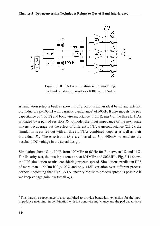
Chapter 5 Downconversion Techniques Robust to Out-of-Band Interference
144
Figure 5.10 LNTA simulation setup, modeling pad and bondwire parasitics (100fF and 1.5nH)
A simulation setup is built as shown in Fig. 5.10, using an ideal balun and external big inductors L=100nH with parasitic capacitance4 of 500fF. It also models the pad capacitance of (100fF) and bondwire inductance (1.5nH). Each of the three LNTAs is loaded by a pair of resistors RL to model the input impedance of the next stage mixers. To average out the effect of different LNTA transconductance (2:3:2), the simulation is carried out with all three LNTAs combined together as well as their individual RL. These resistors (RL) are biased at VCM=600mV to emulate the baseband DC voltage in the actual design. Simulation shows S11<-10dB from 100MHz to 6GHz for RL between 1Ω and 1kΩ. For linearity test, the two input tones are at 801MHz and 802MHz. Fig. 5.11 shows the IIP3 simulation results, considering process spread. Simulations predict an IIP3 of more than +15dBm if RL<100Ω and only ±1dB variation over different process corners, indicating that high LNTA linearity robust to process spread is possible if we keep voltage gain low (small RL).
4 This parasitic capacitance is also exploited to provide bandwidth extension for the input impedance matching, in combination with the bondwire inductance and the pad capacitance [3].

5.4 Chip Implementation
145
IIP3
(dB
m)
100
101
102
1030
5
10
15
20
25
30
with CG,snfp/snsp
with CG,fnfp/fnsp
without CG,nominal
with CG,nominal
RL (Ohm)
Figure 5.11 Simulated LNTA IIP3 versus load impedance (RL) for different process corners (sn: slow-NMOS, sp: slow-PMOS, fn: fast-NMOS, fp: fast-PMOS)
Actually, it turns out that the addition of the CG-stage in parallel to the inverters has a nonlinearity cancellation effect that improves IIP3 for RL between about 20Ω and 200Ω, which determines the Vds-related distortion terms (for the case without a CG-stage, see the grey curve in Fig. 5.11). Simulation and analysis indicate that it is mainly the pre-distortion at the inverter inputs introduced by the CG-stage via its source current, to cancel the distortion generated by inverter itself. Nevertheless, since we are interested in using a low RL value, produced by mixer switches, to deliver signal current into the TIA stage, here we don’t discuss this effect further. A differential LNTA requires an off-chip balun if a single-ended antenna or RF filter is used. Compared to an LNTA with single-ended input, although the differential one may double the power consumption [25], it can render better IIP2. Besides, the input voltage swing on each of the differential inputs is lowered by 3dB, which improves LNTA IIP3 and P1dB by 3dB. Using the same setup as Fig. 5.10, simulations with RL=50Ω (the designed input impedance of the mixer) show input referred P1dB=+4dBm, NF<3dB (only including noise from LNTA), and voltage gain=-1dB for each single-ended output

Chapter 5 Downconversion Techniques Robust to Out-of-Band Interference
146
Figure 5.12 Complete connection of the 1st-stage HR (single-ended RF input shown) and the 2nd-stage HR
(low voltage gain as desired for good linearity) with -3dB bandwidth >7GHz. This wide RF bandwidth benefits from the low impedance (real part) at the output of LNTA, which means the dominant pole is located at a very high frequency given a certain capacitance.
5.4.2 Passive Mixer
Each of the three LNTAs with 2:3:2 ratio connects to 8 passive current-commutating mixer arrays driven by 8-phase LO, as shown in Fig. 5.4. The mixers are DC-coupled to the LNTAs for wider bandwidth compared to AC-coupled,

5.4 Chip Implementation
147
which introduces parasitic capacitance. Each mixer array receives 3 differential inputs from LNTAs and all mixer arrays together deliver 4 differential outputs to TIA1, i.e. 8-phase signals with 45° interval. The complete connection from LNTA to TIA1 via passive mixer switches can be found in Fig. 5.12, with single-ended RF input for figure clarity. The passive mixer simply consists of NMOS switches, with bulk tied to source to reduce the body effect, for a minimized Rmixer at a certain VGS. The bulk and source joint node is at the baseband side of the switch, to reduce the effect of parasitic capacitance from substrate. The gate of the mixer switch is AC-coupled to a clock driver and biased so that the maximum VGS=VDD. The mixer switch-on resistance Rmixer is in the order of 50Ω and all mixer switches have the same dimension for good phase accuracy. Besides, the same Rmixer and different LNTA output impedance (3:2:3) also introduce a current division effect which brings the actual 1st-stage weighting ratio different from 2:3:2 but closer to the ideal 1:√2:1 ratio, good for the overall amplitude accuracy. For good NF, we need to minimize clock overlap to avoid a low-ohmic path between TIA inputs that will amplify TIA noise [18]. For the case with 8 TIA inputs this leads to a maximum LO duty cycle of 1/8. Both sides of the mixer, i.e. the output of LNTA and the input of TIA, are biased at the same DC level (around half VDD) ensuring that little DC current flows for a low 1/f noise from the mixer switches. As an alternative to mixer switches working in the linear region when turned on, using switches in the saturation region (e.g. switches in a Gilbert mixer) may also provide low impedance as 1/gm. However, working in the saturation region would require DC current flowing through those switches, degrading 1/f noise.
5.4.3 Accurate Multiphase Clock
Since the amplitude accuracy can be ensured by the 2-stage polyphase HR, the phase inaccuracy is likely to dominate. Based on Appendix B, if the LO duty cycle is “d”, the resulting 3rd HR (1σ) is:
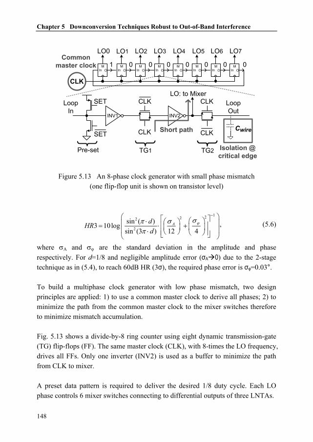
Chapter 5 Downconversion Techniques Robust to Out-of-Band Interference
148
TG1 TG2
SET
SET
CLK
CLK
CLK
CLK
INV1 INV2
Loop In
Loop Out
Pre-set
Cwire
MOIn
MOIn
MOIn
MOIn
MOIn
MOIn
MOIn
MOIn
CLK
1 0 0 0 0 0 0 0
Short path
Isolation @ critical edge
Common master clock
LO: to Mixer
LO1 LO2 LO3 LO4 LO5 LO6 LO7LO0
Figure 5.13 An 8-phase clock generator with small phase mismatch (one flip-flop unit is shown on transistor level)
1222
2
sin ( )3 10logsin (3 ) 12 4
AdHRd
ϕσσππ
−⎛ ⎞⎡ ⎤⎛ ⎞⋅ ⎛ ⎞⎜ ⎟= ⋅ +⎢ ⎥⎜ ⎟⎜ ⎟⎜ ⎟⋅ ⎝ ⎠⎢ ⎥⎝ ⎠⎣ ⎦⎝ ⎠
, (5.6)
where σA and σϕ are the standard deviation in the amplitude and phase respectively. For d=1/8 and negligible amplitude error (σA 0) due to the 2-stage technique as in (5.4), to reach 60dB HR (3σ), the required phase error is σφ=0.03°. To build a multiphase clock generator with low phase mismatch, two design principles are applied: 1) to use a common master clock to derive all phases; 2) to minimize the path from the common master clock to the mixer switches therefore to minimize mismatch accumulation. Fig. 5.13 shows a divide-by-8 ring counter using eight dynamic transmission-gate (TG) flip-flops (FF). The same master clock (CLK), with 8-times the LO frequency, drives all FFs. Only one inverter (INV2) is used as a buffer to minimize the path from CLK to mixer. A preset data pattern is required to deliver the desired 1/8 duty cycle. Each LO phase controls 6 mixer switches connecting to differential outputs of three LNTAs.

5.4 Chip Implementation
149
Figure 5.14 Simulation setup for LO phase mismatch, including the effect of real mixer switches
44.92 44.96 45 45.04 45.08
510152025303540
Figure 5.15 Histogram of the simulated phase difference between two adjacent LO outputs (240 Monte Carlo simulation results)
The gates of all the 6 switches are connected together and driven by the same buffer, i.e. INV2, to minimize buffer mismatch.
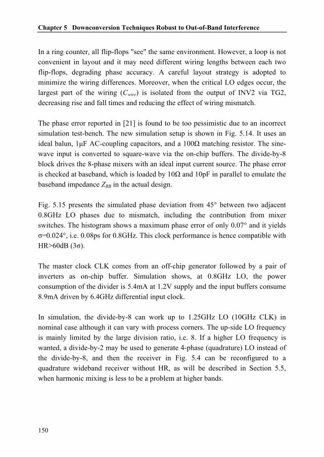
Chapter 5 Downconversion Techniques Robust to Out-of-Band Interference
150
In a ring counter, all flip-flops "see" the same environment. However, a loop is not convenient in layout and it may need different wiring lengths between each two flip-flops, degrading phase accuracy. A careful layout strategy is adopted to minimize the wiring differences. Moreover, when the critical LO edges occur, the largest part of the wiring (Cwire) is isolated from the output of INV2 via TG2, decreasing rise and fall times and reducing the effect of wiring mismatch. The phase error reported in [21] is found to be too pessimistic due to an incorrect simulation test-bench. The new simulation setup is shown in Fig. 5.14. It uses an ideal balun, 1μF AC-coupling capacitors, and a 100Ω matching resistor. The sine-wave input is converted to square-wave via the on-chip buffers. The divide-by-8 block drives the 8-phase mixers with an ideal input current source. The phase error is checked at baseband, which is loaded by 10Ω and 10pF in parallel to emulate the baseband impedance ZBB in the actual design. Fig. 5.15 presents the simulated phase deviation from 45° between two adjacent 0.8GHz LO phases due to mismatch, including the contribution from mixer switches. The histogram shows a maximum phase error of only 0.07° and it yields σ=0.024°, i.e. 0.08ps for 0.8GHz. This clock performance is hence compatible with HR>60dB (3σ).
The master clock CLK comes from an off-chip generator followed by a pair of inverters as on-chip buffer. Simulation shows, at 0.8GHz LO, the power consumption of the divider is 5.4mA at 1.2V supply and the input buffers consume 8.9mA driven by 6.4GHz differential input clock.
In simulation, the divide-by-8 can work up to 1.25GHz LO (10GHz CLK) in nominal case although it can vary with process corners. The up-side LO frequency is mainly limited by the large division ratio, i.e. 8. If a higher LO frequency is wanted, a divide-by-2 may be used to generate 4-phase (quadrature) LO instead of the divide-by-8, and then the receiver in Fig. 5.4 can be reconfigured to a quadrature wideband receiver without HR, as will be described in Section 5.5, when harmonic mixing is less to be a problem at higher bands.
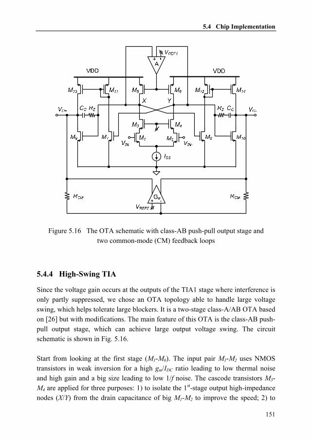
5.4 Chip Implementation
151
Figure 5.16 The OTA schematic with class-AB push-pull output stage and two common-mode (CM) feedback loops
5.4.4 High-Swing TIA
Since the voltage gain occurs at the outputs of the TIA1 stage where interference is only partly suppressed, we chose an OTA topology able to handle large voltage swing, which helps tolerate large blockers. It is a two-stage class-A/AB OTA based on [26] but with modifications. The main feature of this OTA is the class-AB push-pull output stage, which can achieve large output voltage swing. The circuit schematic is shown in Fig. 5.16. Start from looking at the first stage (M1-M6). The input pair M1-M2 uses NMOS transistors in weak inversion for a high gm/IDC ratio leading to low thermal noise and high gain and a big size leading to low 1/f noise. The cascode transistors M3-M4 are applied for three purposes: 1) to isolate the 1st-stage output high-impedance nodes (X/Y) from the drain capacitance of big M1-M2 to improve the speed; 2) to

Chapter 5 Downconversion Techniques Robust to Out-of-Band Interference
152
improve the output impedance of first stage and therefore to improve the OTA voltage gain, which is crucial for a high closed-loop in-band linearity; 3) to prevent the relatively high voltage swing at the X/Y nodes from seeing the drain of M1-M2, so to reduce the effect of channel-length modulation. The PMOS loads M5-M6 use a large VGS and VDS and a large length, which lead to low thermal and 1/f noise and a high output impedance comparable to Rout from the NMOS side M1-M4. At nodes X/Y, enough voltage headroom is reserved to handle more than 250mV peak-to-peak voltage swing on each side. For the OTA’s second stage (M7-M14), a class-AB push-pull output stage is used, which can handle more than 2V peak-to-peak differential output voltage swing at VDD=1.2V. This push-pull capability is obtained via the current mirrors M11-M14, whose DC current can be well defined by the common-mode level of the first-stage outputs. To ensure a low overdrive voltage for high output voltage swing and at the same time to accommodate the relatively high common-mode level at the X/Y nodes due to the cascode transistors M3-M4, high-VTH NMOS transistors M7-M10 are used, which are naturally available in the standard digital CMOS process without adding any extra cost. For the differential-mode feedback (DMFB) loop, Miller compensation via resistor RZ and capacitor CC guarantees 55° minimum phase margin over all process corners. Due to the use of a current mirror, the common-mode output voltage of the second stage is not influenced by that of the first stage. Therefore, two common-mode feedback (CMFB) loops are required in this OTA, i.e. a voltage-sense voltage-control loop for the first stage and a voltage-sense current-control loop for the second stage respectively, as shown in Fig. 5.16. In our design, the difference from what was presented in [26] are mainly two points: 1) the input pair is changed from PMOS to NMOS (M1-M2) to accommodate the DC voltage at the virtual-ground node, which is defined by LNTA to be half VDD for maximum voltage swing (Fig. 5.4); 2) the addition of cascode transistors M3-M4 for improved performance as discussed before. Each OTA draws 3.2mA from 1.2V supply, with 2mA in the first stage and 1mA in the second stage while two CMFB loops and bias circuitry together consume
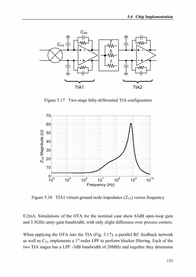
5.4 Chip Implementation
153
CVG
-
+ -
+ -
+ -
+
7
5
7
TIA1 TIA2
CFB
Figure 5.17 Two-stage fully-differential TIA configuration
104 105 106 107 108 109 10100
10
20
30
40
50
60
70
Frequency (Hz)
Z VG M
agni
tude
(Ω)
Figure 5.18 TIA1 virtual-ground node impedance (ZVG) versus frequency
0.2mA. Simulations of the OTA for the nominal case show 63dB open-loop gain and 3.5GHz unity-gain bandwidth, with only slight difference over process corners. When applying the OTA into the TIA (Fig. 5.17), a parallel RC feedback network as well as CVG implements a 1st-order LPF to perform blocker filtering. Each of the two TIA stages has a LPF -3dB bandwidth of 20MHz and together they determine

Chapter 5 Downconversion Techniques Robust to Out-of-Band Interference
154
the receiver IF bandwidth of 12MHz, which may accommodate most mobile communication standards. The virtual-ground impedance (ZVG) of the TIA1, as shown in Fig. 5.18, has a magnitude of about 4Ω around DC and peaks to 60Ω around 700MHz due to a lowered loop gain while a 5pF CVG brings impedance down at higher frequencies. Applying (5.3) to multiply ZVG with a coefficient of 0.12 and consider Rmixer=50Ω, we know that Rmixer will dominate the mix-impedance value at node B of Fig. 5.2. The two TIA stages use the same OTA design but different component values in the RC feedback. The feedback resistor of the TIA1 stage is 1kΩ and that of the TIA2 stage is 2kΩ. The simulated gain of the receiver after the TIA1 stage is 27dB and after the TIA2 stage the gain is 34dB.
5.4.5 Baseband R-net
The resistor network (R-net) provides the 2nd-stage weighting for HR. It also converts 8-phase outputs of the TIA1 stage into quadrature inputs of the TIA2 stage. To form a 5:7:5 amplitude ratio, 19 unit-resistors form a resistance ratio of 7:5:7 in 3 paths. As shown in Fig. 5.12, the R-net consists of weighted resistor groups each with a ratio of 7:5:7 and there are 8 groups in total to interface the 8 outputs of TIA1 stage. Harmonic rejection at baseband (via R-net) can also reduce errors due to parasitic capacitance compared to at high frequency.
5.5 Receiver Frequency Range Extension The divide-by-8 is used to generate accurate LO phases for HR, which requires the common master clock frequency to be 8-times the LO frequency. Indeed the LO path limits the receiver frequency range to 1.25GHz (simulation). However, the signal-path bandwidth should be much wider as mentioned in Section 5.4.1 because: 1) minimum-length transistors (65nm) are used in the LNTA which guarantees S11<-10dBm up to 6GHz as simulated; 2) a low real impedance is presented to the output of the LNTA so that the RC time constant is small, which allows a -3dB bandwidth of 7GHz in simulation. To explore the wideband property, we should extend the LO frequency range.

5.5 Receiver Frequency Range Extension
155
RF+-
8
8
-+-
+
-+-
+
-+-
+
-+-
+
TIA14PM8PM
Q+
-
-+-
+
-+-
+
I+
-
TIA2
757
757
757
757
R-net
ModeSelect
2Gm
2Gm
3Gm
50Ω
50Ω
LNTA
CLK+-
100Ω
42
Figure 5.19 Reconfigurable 0.4-to-5GHz receiver block diagram
If a higher LO frequency is wanted, a divide-by-2 may be used to generate 4-phase (quadrature) LO, instead of the divide-by-8, which can be expected to extend the LO frequency by 4 times assuming the same maximum speed of the master clock. Since harmonic mixing is mainly problematic for relatively low LO frequencies, e.g. <1GHz, as observable from Fig. 1.1 of spectrum allocation, the 4-phase LO can be used as an alternative at high bands. Then the 2-stage polyphase HR architecture (Fig. 5.4) can be made reconfigurable by adding a quadrature 4-phase mixer driven by a 4-phase LO in parallel to the presented 8-phase mixer to extend the receiver’s frequency range. Fig. 5.19 shows the block diagram of the extended receiver with a 4-phase mixer added, driven by a 25%-duty-cycle LO generated via a divide-by-2, which can still
Chapter 5 Downconversion Techniques Robust to Out-of-Band Interference
156
generate accurate balanced LO to reject the even-order harmonics. Which divider is enabled (via Mode Select) determines either the 4-phase mixer (4PM) or the 8-phase mixer (8PM) in use. In case of the 4-phase mixer, the divide-by-2 is enabled while the divide-by-8 is disabled and the gate bias voltages are set to GND for all 8-phase mixer switches. Both mixers share the same switch size. The 4-phase mixer consists of 4 mixer arrays in parallel each driven by an LO phase. Each mixer array consists of 6 NMOS switches which receive 3 differential inputs from LNTAs and all mixer arrays together deliver I/Q differential outputs to the virtual ground nodes of the TIA2 stage while the TIA1 stage can be shut down to save power. Big-sized NMOS switches are applied between the R-net and the TIA2 stage, which only turn on when the 8-phase mixer is in use. When the receiver is configured to the 4-phase mode, the feedback resistor of the TIA2 stage is set to 1kΩ to keep about the same receiver gain (~34dB) while 2kΩ was used in the 8-phase mode and extra capacitors are connected to maintain the IF bandwidth of 20MHz. Still, the low-pass blocker filtering is effective since the 1st voltage gain occurs at baseband after the LPF of the TIA2 stage. The whole reconfigurable 4/8-phase receiver including the divide-by-2/8 has been realized in schematic transistor-level and simulation has been done using all real components. In simulation, the divide-by-2 works up to 5GHz LO (master clock at 10GHz). The gain is consistently around 33dB and the NF is around 4dB up to 5GHz RF while the IIP3 is +5dBm. Please note that the power consumption in the 4-phase mode can be 12mA lower than the 8-phase mode since the TIA1 stage is turned off. These results show the promise to reconfigure the 2-stage polyphase HR system to achieve a broader RF range. Unfortunately, due to limited time, the reconfigurable receiver was only ready in schematics but was not integrated into the final chip layout. Nevertheless, the basic ideas of building SDR receivers robust to OBI, via the low-pass blocker filtering and the 2-stage polyphase HR techniques, can already be demonstrated via the 8-phase receiver path. The wideband property of the receiver signal-path can also be proved by measurement, as to be shown in Section 5.6.1.
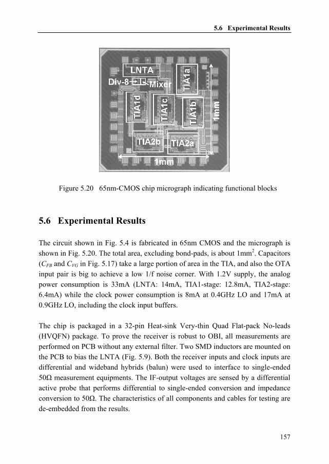
5.6 Experimental Results
157
Figure 5.20 65nm-CMOS chip micrograph indicating functional blocks
5.6 Experimental Results The circuit shown in Fig. 5.4 is fabricated in 65nm CMOS and the micrograph is shown in Fig. 5.20. The total area, excluding bond-pads, is about 1mm2. Capacitors (CFB and CVG in Fig. 5.17) take a large portion of area in the TIA, and also the OTA input pair is big to achieve a low 1/f noise corner. With 1.2V supply, the analog power consumption is 33mA (LNTA: 14mA, TIA1-stage: 12.8mA, TIA2-stage: 6.4mA) while the clock power consumption is 8mA at 0.4GHz LO and 17mA at 0.9GHz LO, including the clock input buffers. The chip is packaged in a 32-pin Heat-sink Very-thin Quad Flat-pack No-leads (HVQFN) package. To prove the receiver is robust to OBI, all measurements are performed on PCB without any external filter. Two SMD inductors are mounted on the PCB to bias the LNTA (Fig. 5.9). Both the receiver inputs and clock inputs are differential and wideband hybrids (balun) were used to interface to single-ended 50Ω measurement equipments. The IF-output voltages are sensed by a differential active probe that performs differential to single-ended conversion and impedance conversion to 50Ω. The characteristics of all components and cables for testing are de-embedded from the results.

Chapter 5 Downconversion Techniques Robust to Out-of-Band Interference
158
0.4 0.5 0.6 0.7 0.8 0.932
32.5
33
33.5
34
34.5
35
0.4 0.5 0.6 0.7 0.8 0.9 3
3.5
4
4.5
5
5.5
6
Gain
NF
Figure 5.21 Measured voltage gain and NF of the 2-stage receiver versus LO frequency
The divide-by-8 works up to 0.9GHz LO, and the measured S11 is lower than -10dB up to 5.5GHz. This means the HR measurement is valid for 0.9GHz LO up to its 6th harmonic. The measured IF bandwidth is 12MHz and the baseband 1/f noise corner is 30kHz thanks to the passive mixer with little DC current and the OTA with a large-sized input pair.
5.6.1 Gain, NF, in-band IIP2/IIP3, and RF bandwidth
Fig. 5.21 shows the measured voltage gain and DSB NF over an LO frequency of 0.4 to 0.9GHz. The voltage conversion gain, measured for an IF of 1MHz from the input of the balun to the differential outputs of receiver, is above 34dB over the whole band and is quite flat (±0.2dB variation), indicating a much wider RF bandwidth. The NF is measured for an IF of 10MHz since the available NF analyzer (Agilent N8973A) starts from that frequency. The DSB NF is below 4dB except for 0.4GHz where 1/f noise from the LNTA starts to dominate. Fig. 5.22 shows the measured in-band (IB) IIP2 and IIP3 over LO frequency, with two tones close to the LO frequency fLO so that they are not affected by IF filtering (IIP2: fLO+3MHz and fLO+6.01MHz; IIP3: fLO+3MHz and fLO+3.01MHz). After

5.6 Experimental Results
159
0.4 0.5 0.6 0.7 0.8 0.94243444546474849
0.4 0.5 0.6 0.7 0.8 0.9 2.533.544.555.56
IIP2
IIP3
Figure 5.22 Measured in-band IIP2 and IIP3 versus LO frequency downconversion, the IM2 component at 3.01MHz and the IM3 component at 2.99MHz are measured. The IB IIP3 is around +3.5dBm, which is good given the high gain of 34dB, thanks to only voltage gain at baseband with negative feedback. The IB IIP2 is above +46dBm. The divide-by-8 limits the LO frequency range up to 0.9GHz (master clock @ 7.2GHz), but the signal-path -3dB RF bandwidth is much wider, up to 6GHz. To verify it, we conducted a gain measurement for the 7th harmonic, i.e. the first non-canceled high-order harmonic. Ideally, using 1/8 duty-cycle LO, the strength of the 7th harmonic should be 1/7 of the fundamental harmonic, so we expect the 7th harmonic should ideally have a gain that is 16.9dB (1/7) lower from 34dB, i.e. 17.1dB. Indeed, as shown in Fig. 5.23, the gain drops from 17dB at 0.7GHz RF to 14.3dB at 6GHz RF (LO: 0.1 to 0.85GHz), which means the OBI will only be attenuated a little by the frequency roll-off at RF. It also indicates that the receiver can be readily expanded to cover higher bands by extending the LO range as discussed in Section 5.5.

Chapter 5 Downconversion Techniques Robust to Out-of-Band Interference
160
0.5 1 1.5 2 2.5 3 3.5 4 4.5 5 5.5 6 6.513.5
14
14.5
15
15.5
16
16.5
17
17.5
RF (GHz)
Gai
n (d
B)
measured gainof 7th harmonic
Figure 5.23 Measured voltage gain of 7th harmonic indicating a signal-path -3dB bandwidth of 6GHz (IF=1MHz, RF=7·fLO+1MHz)
5.6.2 Out-of-Band IIP2/IIP3
We also measured the out-of-band (OB) IIP2 and IIP3. Due to the LPF behavior, the measured OB linearity depends on the distance from fLO to the two RF tones used. For sufficient distance, the LPF will suppress the downconverted two-tone interference so the OB nonlinearity is mainly contributed by the V-I of the LNTA. The OB IIP3 is tested via two tones at 1.61GHz and 2.40GHz with an LO at 819MHz, so that the IM3 is at 820MHz RF and 1MHz IF. The results of both IB (0.8GHz LO) and OB IIP3 are shown in Fig. 5.24. Without fine tuning, the measured OB IIP3 is +16dBm, which agrees with the simulated results in Fig. 5.11. Compared to the IB IIP3 of +3.5dBm, the OB IIP3 is dramatically improved because the TIA was dominating the IB IIP3, due to the high voltage gain at the output. As shown in the figure, the range for which IM3 follows the extrapolation line is also improved by almost 20dB (upper limit of -30dBm for IB versus -10dBm for OB). This is crucial to tolerate large OB interference.
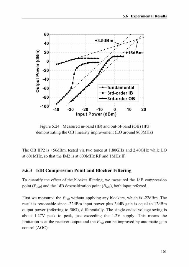
5.6 Experimental Results
161
-40 -30 -20 -10 0 10 20-100
-80
-60
-40
-20
0
20
40
60
Input Power (dBm)
Out
put P
ower
(dB
m)
fundamental3rd-order IB3rd-order OB
+3.5dBm
+16dBm
Figure 5.24 Measured in-band (IB) and out-of-band (OB) IIP3 demonstrating the OB linearity improvement (LO around 800MHz)
The OB IIP2 is +56dBm, tested via two tones at 1.80GHz and 2.40GHz while LO at 601MHz, so that the IM2 is at 600MHz RF and 1MHz IF.
5.6.3 1dB Compression Point and Blocker Filtering
To quantify the effect of the blocker filtering, we measured the 1dB compression point (P1dB) and the 1dB desensitization point (B1dB), both input referred. First we measured the P1dB without applying any blockers, which is -22dBm. The result is reasonable since -22dBm input power plus 34dB gain is equal to 12dBm output power (referring to 50Ω), differentially. The single-ended voltage swing is about 1.27V peak to peak, just exceeding the 1.2V supply. This means the limitation is at the receiver output and the P1dB can be improved by automatic gain control (AGC).

Chapter 5 Downconversion Techniques Robust to Out-of-Band Interference
162
0.4 0.8 1.2 1.6 2 2.4 2.8 3.2 3.6 4-24
-21
-18
-15
-12-9
-6
-3
03
Figure 5.25 Measured 1dB desensitization point (B1dB) versus blocker frequency A more serious problem is to receive a weak signal at the same time with a strong interferer: a so-called blocker test. In this situation AGC doesn't help since the maximum gain is required to maintain sensitivity. The measurement was carried out with the LO at 400MHz and the desired RF signal at 401MHz with -50dBm input power. The blocker frequency is varied from 402MHz to 4.002GHz. Fig. 5.25 shows B1dB versus the blocker frequency. As predicted by (5.1) and (5.2), we see two effects in the figure: 1) the tolerable blocker power depends on the frequency distance between the LO and the blocker, due to the LPF behavior5; 2) HR also plays a role in blocker filtering, as two dips occur around 7th and 9th harmonics of the LO frequency, both of which are not rejected well by the 8-phase HR. From the figure, we can observe that B1dB is better than P1dB (-22dBm) except very close-by blockers (402MHz) and the maximum B1dB is more than 0dBm, showing the blocker filtering is indeed effective.
5 The actual behavior of the LPF is more complicated than (5.2), since our baseband filter is cascaded in two stages, which does not follow a simple 1st-order or 2nd-order filtering behavior.

5.6 Experimental Results
163
0.4 0.5 0.6 0.7 0.8 0.920
30
40
50
60
70
8080
LO Frequency (GHz)
HR
Rat
io (d
B)
1-stage only
2-stage total
5th
3rd
5th
3rd
Figure 5.26 Measured HR ratio versus LO frequency: comparison between HR with only 1-stage and total 2-stage
5.6.4 Harmonic Rejection
First we look at the 2-stage polyphase HR. The HR ratio can be measured by comparing the gain difference between the desired signal and the harmonic image. At the receiver input, the desired signal power was -50dBm while the harmonic image power was -30dBm.
Fig. 5.26 shows, for one chip, the HR of 1-stage, at the outputs of the TIA1, and the total 2-stage HR, at the outputs of the TIA2, versus LO frequency. The HR of 1-stage is between 30 and 40dB and the HR of 2-stage is around 70dB, which represents a 30dB improvement for both 3rd and 5th HR thanks to the 2-stage polyphase HR technique. Generally, the HR improvement from 1-stage to 2-stage is in the range of 20 to 40dB as observed from multiple chips. The large improvement also shows that it is the amplitude error dominating the 1st-stage HR. To identify the effect of mismatch, we measured the HR of 2-stage for 40 chips at 0.8GHz LO, as shown in Fig. 5.27. The minimum 3rd order HR is 60dB and the minimum 5th order HR is 64dB. The 2nd, 4th, and 6th HR is also measured, over 20 chips. The minimum 2nd-order HR is 62dB, while the minimum 4th and 6th order

Chapter 5 Downconversion Techniques Robust to Out-of-Band Interference
164
10 20 30 401
60
70
80
90
Sample #
HR
Rat
io (d
B)
5th3rd
Figure 5.27 Measured HR ratio of 40 chips at 800MHz LO HR are both 67dB. These results are achieved without calibration, trimming, or RF filtering. Since the signal-path -3dB RF bandwidth has been characterized to be up to 6GHz, the contribution of the frequency roll-off to the HR result should be small. According to (5.6), the simulated phase error σ=0.024° means a minimum HR (3σ) of 62dB if the amplitude error is eliminated, fitting well with the measured HR as well as the Monte Carlo simulation results. This also suggests that phase error can indeed be the limitation now. As mentioned at the end of Section 5.3. To further correct phase error, digitally-enhanced HR can be applied, whose measurement results will be briefly mentioned here as a comparison (Table 5.1).

5.6 Experimental Results
165
a) If one harmonic interference image band is dominating.
Analog 2-stage Digital AIC
Rej. strongest >60 dB >80 dB a)
Rej. other odd >64 dB >36 dB
Rej. even >62 dB >64 dB
Power front-end 50 mA @ 1.2 V(excl. ADCs)
44 mA @ 1.2 V(excl. ADCs)
Power DSP(100 MS/s)
N/A <8.5 mA @ 1.2 V(simulated)
# ADCs 2 4
Analog 2-stage Digital AIC
Rej. strongest >60 dB >80 dB a)
Rej. other odd >64 dB >36 dB
Rej. even >62 dB >64 dB
Power front-end 50 mA @ 1.2 V(excl. ADCs)
44 mA @ 1.2 V(excl. ADCs)
Power DSP(100 MS/s)
N/A <8.5 mA @ 1.2 V(simulated)
# ADCs 2 4
Table 5.1 Comparison of two alternative HR techniques robust to mismatch The 2-stage polyphase HR implemented in analog approach helps both 3rd and 5th HR via improved amplitude accuracy and achieves a minimum rejection of 60dB and 64dB respectively. The digitally-enhanced HR based on AIC algorithm consistently shows more than 80dB of HR for a single harmonic image (either the 3rd or the 5th) by correcting both amplitude and phase of that harmonic image. The other harmonic image is rejected by at least 36 dB, not improved from the analog 1st stage. They share a similar limitation on even-order HR. An interesting and advantageous feature of digitally-enhanced HR is that when interferer is stronger the HR ratio is also larger, benefiting from the adaptive algorithm [1]. On the implementation level, compared to the 2-stage polyphase HR, the digitally-enhanced HR architecture requires two additional A/D converters (Fig. 5.8), which may increase the power considerably. Nevertheless, they may be switched off when the analog HR stages can provide enough harmonic rejection.
5.6.5 Performance Summary and Benchmark
Table 5.2 summarizes the measured performance. As a benchmark, Table 5.3 shows a comparison to other recently published wideband receivers with HR.

Chapter 5 Downconversion Techniques Robust to Out-of-Band Interference
166
LO Frequency 0.4 to 0.9GHzGain 34.4dB± 0.2dB
DSB NF 4dB± 0.5dBS11 < -10dB 80MHz to 5.5GHz
-3dB RF Bandwidth Up to 6GHzIn/Out-of-band IIP3 +3.5dBm / +16dBmIn/Out-of-band IIP2 +46dBm / +56dBm
-3dB IF Bandwidth 12MHz1/f noise 30kHz corner
Harmonic Rejection
Analog 2-stage 2nd-6th: >60dB
Digital AIC 1 strongest: >80dBTechnology 65nm CMOS
Supply Voltage 1.2VDC Current 50mA max.
Table 5.2 Summary of some measured key performance
Benchmark CMOS Tech.
Freq.(MHz)
Gain(dB)
NF(dB)
IIP3 (dBm)
HR3 (dB)
HR5 (dB)
Chip # Cal. Power(mW)
This Work 65nm 400-900 a)
34 4 +3.5 60 64 40 min. No 60LNA + Mixer + Divider
Bagheri, JSSC06 [3]
90nm 800-5000
36 5 -15 b) 38 40 1 No 51LNA + Mixer + Divider, performance at 900MHz
Lerstaveesin, JSSC08 [5]
180nm 48-860
83 4 to 7 -14 42 c) ? 1 No 468 c)
LNA + Mixer + BB filter + VGA + ADC + PLLRu,
ISSCC08 [15]65nm 200-
9002 19 +11 41 44 10 av. No 19
No LNA, only mixer & multiphase clockMaxim,
ISSCC08 [27]130nm 40-
1000? 16 +20 63 64 1 No 450
No LNA, only mixer & multiphase clockCha,
MWCL08 [28]180nm 48-
86235 8 -15 72 45 10 min. Yes 189
LNA + Mixer + Divider
Benchmark CMOS Tech.
Freq.(MHz)
Gain(dB)
NF(dB)
IIP3 (dBm)
HR3 (dB)
HR5 (dB)
Chip # Cal. Power(mW)
This Work 65nm 400-900 a)
34 4 +3.5 60 64 40 min. No 60LNA + Mixer + Divider
Bagheri, JSSC06 [3]
90nm 800-5000
36 5 -15 b) 38 40 1 No 51LNA + Mixer + Divider, performance at 900MHz
Lerstaveesin, JSSC08 [5]
180nm 48-860
83 4 to 7 -14 42 c) ? 1 No 468 c)
LNA + Mixer + BB filter + VGA + ADC + PLLRu,
ISSCC08 [15]65nm 200-
9002 19 +11 41 44 10 av. No 19
No LNA, only mixer & multiphase clockMaxim,
ISSCC08 [27]130nm 40-
1000? 16 +20 63 64 1 No 450
No LNA, only mixer & multiphase clockCha,
MWCL08 [28]180nm 48-
86235 8 -15 72 45 10 min. Yes 189
LNA + Mixer + Dividera) Only LO frequency range, while the measured RF bandwidth is up to 6GHz.b) IIP3 is derived for the full-gain setting which is required to match the 5dB NF.c) Both the HR3 and the power data exclude the contribution of RF tracking filter.
Table 5.3 Benchmark with other recent work

5.7 Conclusions
167
There are two outstanding parameters of this work, i.e. linearity and harmonic rejection. Comparing all work including an LNA, [3], [5], and [28] shows an IIP3 around -15dBm while this work shows an IIP3 of +3.5dBm and a competitive NF. The OB IIP3 of our work is even higher (+16dBm), but we didn’t find a good way to benchmark it. For HR, only [27] and [28] reported numbers comparable to this work. However, [27] only reported results from one chip while consuming large power due to a different structure of the HR mixer. [28] reported results for 10 chips, but relying on hand calibration, and the calibration is only effective for either 3rd or 5th HR but not for both at the same time. Thus we conclude that our design has both good linearity and good HR at moderate power consumption, thanks to the proposed techniques.
5.7 Conclusions This chapter has addressed two main problems for out-of-band interference (OBI): out-of-band (OB) nonlinearity and harmonic mixing. First, OB nonlinearity can be improved by low-pass (LP) blocker filtering, i.e. making voltage gain only at baseband simultaneously with LP filtering to improve the OB IIP3 and the desensitization point due to blockers. We have also presented a comprehensive analysis of mix-impedance (see Appendix A) which can deliver a low impedance at RF by transferring the baseband impedance through passive mixers. Second, an “iterative” HR technique, i.e. a 2-stage polyphase HR concept, is proposed. It realizes HR in cascaded stages which can greatly enhance the amplitude accuracy for both 3rd and 5th HR so that the total amplitude error becomes the product of errors from each stage. To guarantee a small phase error, a simple but accurate ring counter is presented to generate the multiphase clocks driving the HR mixer. Together they provide mismatch-robust HR. To quantify the achievable HR with certain mismatch, the effects of random amplitude and phase errors to HR are also analyzed (see Appendix B). We have verified the proposed techniques via a SDR receiver in 65nm CMOS, with RF bandwidth up to 6GHz and 8-phase LO frequency up to 0.9GHz (master clock up to 7.2GHz). The 1dB compression point is -22dBm while the maximum 1dB desensitization point is more than 0dBm, showing the LP blocker filtering is

Chapter 5 Downconversion Techniques Robust to Out-of-Band Interference
168
effective. In terms of IIP3, +16dBm for OBI is measured without fine tuning for sufficient frequency spacing, e.g. LO at 819MHz while two-tone at 1.61G and 2.40GHz, versus an in-band IIP3 of +3.5dBm. Without any trimming or calibration, the 2-stage polyphase HR technique achieves 60dB minimum HR ratio at 0.8GHz LO for both 3rd and 5th harmonics over 40 randomly-selected chips. All even-order HR ratios are measured to be above 60dB as well. The benchmarking shows that this work achieves the highest IIP3 and the most-robust HR without compromising other performance such as NF and power consumption.
5.8 References [1] Z. Ru, N. Moseley, E. Klumperink, B. Nauta, “Digitally-Enhanced Software-
Defined Radio Receiver Robust to Out-of-Band Interference”, accepted by IEEE J. Solid-State Circuits, Dec. 2009
[2] V. Giannini, P. Nuzzo, C. Soens, et. al., “A 2mm 0.1G-to-5GHz SDR Receiver in 45nm Digital CMOS”, IEEE ISSCC, Dig. Tech. Papers, pp.408-409, Feb. 2009
[3] R. Bagheri, A. Mirzaei, S. Chehrazi, et. al., "An 800-MHz–6-GHz Software-Defined Wireless Receiver in 90-nm CMOS", IEEE J. Solid-State Circuits, vol.41, no.12, pp.2860-2876, Dec. 2006
[4] F. Gatta, R. Gomez, Y. Shin, et al., “An Embedded 65nm CMOS Low-IF 48MHz-to-1GHz Dual Tuner for DOCSIS 3.0”, IEEE ISSCC, Dig. Tech. Papers, pp.122-123, Feb. 2009
[5] S. Lerstaveesin, M. Gupta, D. Kang and B.-S. Song, "A 48–860 MHz CMOS Low-IF Direct-Conversion DTV Tuner," IEEE J. Solid-State Circuits, vol.43, no.9, pp.2013-2024, Sept. 2008
[6] S.C. Blaakmeer, E. Klumperink, D.M.W. Leenaerts and B. Nauta, "The Blixer, a Wideband Balun-LNA-I/Q-Mixer Topology," IEEE J. Solid-State Circuits, vol.43, no.12, pp.2706-2715, Dec. 2008
[7] D Leenaerts, R. van de Beek, J. Bergervoet, et. al., “A 65nm CMOS Inductorless Triple-Band-Group WiMedia UWB PHY”, IEEE ISSCC, Dig. Tech. Papers, pp.410-411, Feb. 2009
[8] D. Manstretta, N. Laurenti and R. Castello, "A Reconfigurable Narrow-Band MB-OFDM UWB Receiver Architecture," IEEE Trans. Circuits and Systems II: Express Briefs, vol.55, no.4, pp.324-328, Apr. 2008
5.8 References
169
[9] T. Sowlati, B. Agarwal, J. Cho, J.; et al., “Single-Chip Multiband WCDMA/ HSDPA/HSUPA/EGPRS Transceiver with Diversity Receiver and 3G DigRF Interface Without SAW Filters in Transmitter / 3G Receiver Paths”, IEEE ISSCC, Dig. Tech. Papers, pp.116-117, Feb. 2009
[10] O. Gaborieau, S. Mattisson, N. Klemmer, et al., “A SAW-less Multiband WEDGE Receiver”, IEEE ISSCC, Dig. Tech. Papers, pp.114-115, Feb. 2009
[11] V. Aparin and L.E. Larson, "Modified derivative superposition method for linearizing FET low-noise amplifiers," IEEE Trans. Microwave Theory and Techniques, vol.53, no.2, pp.571-581, Feb. 2005
[12] Wei-Hung Chen, Gang Liu, B. Zdravko and A.M. Niknejad, "A Highly Linear Broadband CMOS LNA Employing Noise and Distortion Cancellation," IEEE J. Solid-State Circuits, vol.43, no.5, pp.1164-1176, May 2008
[13] E.A.M. Klumperink, B. Nauta, "Systematic comparison of HF CMOS transconductors," IEEE Trans. Circuits and Systems II: Analog and Digital Signal Processing, vol.50, no.10, pp. 728-741, Oct. 2003
[14] J.A. Weldon, R.S. Narayanaswami, J.C. Rudell, et. al., "A 1.75-GHz highly integrated narrow-band CMOS transmitter with harmonic-rejection mixers," IEEE J. Solid-State Circuits, vol.36, no.12, pp.2003-2015, Dec. 2001
[15] Z. Ru, E. Klumperink, and B. Nauta, "A Discrete-Time Mixing Receiver Architecture with Wideband Harmonic Rejection," IEEE ISSCC, Dig. Tech. Papers, pp.322-616, Feb. 2008
[16] H. Darabi, "A Blocker Filtering Technique for SAW-less Wireless Receivers," IEEE J. of Solid-State Circuits, vol.42, no.12, pp.2766-2773, Dec. 2007
[17] B. Razavi, “RF Microelectronics”, Prentice Hall, Upper Saddle River, NJ, 1998
[18] W. Redman-White and D.M.W. Leenaerts, "1/f noise in passive CMOS mixers for low and zero IF integrated receivers," ESSCIRC, Proc., pp. 41-44, 18-20 Sept. 2001
[19] M. Valla, G. Montagna, R. Castello, et. al., "A 72-mW CMOS 802.11a direct conversion front-end with 3.5-dB NF and 200-kHz 1/f noise corner," IEEE J. Solid-State Circuits, vol.40, no.4, pp. 970-977, Apr. 2005
[20] D. Kaczman, M. Shah, M. Alam, et. al., "A Single–Chip 10-Band WCDMA/HSDPA 4-Band GSM/EDGE SAW-less CMOS Receiver With DigRF 3G Interface and +90 dBm IIP2," IEEE J. Solid-State Circuits, vol.44, no.3, pp.718-739, Mar. 2009

Chapter 5 Downconversion Techniques Robust to Out-of-Band Interference
170
[21] Z. Ru, E. Klumperink, G. Wienk and B. Nauta, “A Software-Defined Radio Receiver Architecture Robust to Out-of-Band Interference”, IEEE ISSCC, Dig. Tech. Papers, pp.230-231, Feb. 2009
[22] N.A. Moseley, E. Klumperink, and B. Nauta, "A Two-Stage Approach to Harmonic Rejection Mixing Using Blind Interference Cancellation," IEEE Trans. Circuits and Systems II: Express Briefs, vol.55, no.10, pp.966-970, Oct. 2008
[23] F. Bruccoleri, E.A.M. Klumperink, B. Nauta, "Wide-band CMOS low-noise amplifier exploiting thermal noise canceling," IEEE J. Solid-State Circuits, vol.39, no.2, pp. 275-282, Feb. 2004
[24] B. Razavi, “Design of Analog CMOS Integrated Circuits”, McGraw-Hill, 2000
[25] T. H. Lee, “The Design of CMOS Radio-Frequency Integrated Circuits”, 2nd Edition, Cambridge University Press, 2003
[26] S. Rabii and B.A. Wooley, "A 1.8-V digital-audio sigma-delta modulator in 0.8-μm CMOS," IEEE J. Solid-State Circuits, vol.32, no.6, pp.783-796, June 1997
[27] A. Maxim, R. Poorfard, M. Reid, et. al., “A DDFS Driven Mixing-DAC with Image and Harmonic Rejection Capabilities”, IEEE ISSCC Dig. Tech. Papers, pp.372-373, Feb. 2008
[28] H. Cha, S. Song, H. Kim, K. Lee, "A CMOS Harmonic Rejection Mixer With Mismatch Calibration Circuitry for Digital TV Tuner Applications," IEEE Microwave and Wireless Components Letters, vol.18, no.9, pp.617-619, Sept. 2008

171
Chapter 6 Conclusions
This final chapter summarizes the work being described in Chapter 1 to Chapter 5, and it also provides an outlook to future work on software-defined radios. Section 6.1 presents the summary and conclusions of this thesis and Section 6.2 highlights the original contributions of this work. Section 6.3 suggests some future work. The references are listed in Section 6.4. 6.1 Summary and Conclusions
This thesis is dedicated to two aspects of realizing software-defined radio (SDR) receivers: 1) the challenge of realizing SDR receivers compatible with CMOS scaling and SoC integration; 2) the challenge of realizing SDR receivers robust to out-of-band interference (OBI). We have mainly focused on frequency translation techniques to address these challenges and have also investigated some filter and amplifier techniques to support the receivers’ robustness to OBI. We have contributed to the theory of frequency translation (FT) in radios and have also proposed and verified several new concepts in deep-sub-micron CMOS technology.
Chapter 1
We started from describing the origins of the terms “software radio” (SWR) and “software-defined radio” (SDR) which were not always clear. Based on literature review, we have clarified these two terms and suggested that SWR can be regarded as software-intensive SDR, illustrated by a phase space of radio evolution towards greater programmability.

Chapter 6 Conclusions
172
Being aware of the fact that a SDR should preferably be implemented in CMOS together with digital hardware on the same chip, for feasibility at this moment we still need the analog front-end (AFE) in a SDR receiver to ease the requirements of ADC. After setting our thesis scope on the AFE, we have recognized four specific challenges of a SDR receiver compared to a traditional receiver. For each point of these challenges, discussions are expanded to clarify their implications and some state-of-the-art solutions are briefly reviewed to present the progress towards SDR. Two challenges, i.e. wideband receivers and flexible channel-selection filters, appear close to be solved by other work. Then concrete research objectives are defined mainly in line with the other two challenges: 1) compatibility with CMOS scaling and SoC integration; 2) robustness to out-of-band interference. Specifically, we conclude that frequency translation (FT) techniques deserve attention.
Chapter 2
An overview of different FT techniques for radio receivers has been given by means of classification, based on downconversion principles (mixing or sampling) and input signal domains (continuous or discrete in both time and amplitude). A comparison of the mixing and sampling principles reveals their fundamental differences: in the time domain, for sampling the information rate changes while for mixing it keeps the same; in the frequency domain, mixing always performs frequency translation while sampling may or may not, depending on the relationship between the input and the sampling frequency. A mathematical derivation of the sampling process proves the importance of the step of conversion from continuous-time (CT) domain with an infinite information rate to discrete-time (DT) domain with a finite information rate. Furthermore, based on various FT techniques, three receiver architectures come up. All architectures have been evaluated for their suitability to SDR receivers and it can be argued that both RF-mixing and RF-sampling receivers are suitable, each with their own advantages and drawbacks. The advantages of RF-sampling receivers include the compatibility with CMOS scaling and SoC integration. The drawback is the implementation complexity due to the clock generation/routing and the RF-related baseband processing. To explore the potential of RF sampling for wideband SDR receivers, three specific challenges are identified and analyzed

6.1 Summary and Conclusions
173
quantitatively: frequency-dependent phase shift, aliasing of noise and interference, and frequency-dependent conversion gain of charge sampling.
Chapter 3
The classification of FT techniques also leads to the definition of a new FT technique: DT mixing, which is based on the mixing principle with an analog-DT input signal. It is a variation of RF-sampling receivers but more suitable for wideband applications as it features wideband phase shift and wideband harmonic rejection (HR). Preceded by voltage sampling whose conversion gain is not systematically dependent on sampling frequency, the DT mixing architecture can relieve the three challenges mentioned in the previous paragraph. The DT mixing concept has been verified by a 200-to-900MHz downconverter chip built in 65nm CMOS, employing an 8-times oversampler realized via time-interleaved sampling followed by an I/Q DT HR mixer realized via de-multiplexing. The chip consumes less than 20mW power including a multiphase clock generator. It achieves a best-in-class NF (18 to 20dB) compared to other voltage sampling based RF downconverters, thanks to oversampling and rejection of noise folding by HR. It can reject the 2nd-to-6th harmonic mixing, however the worst-case HR is limited to around 25dB in the current design, due to amplitude errors and especially severe phase mismatches.
Chapter 4
To improve the NF and the HR of the downconverter chip as well as to build a complete RF-sampling receiver, a tunable LC filter and a linearized LNA are added as pre-stages. To obtain a high Q and to save chip area, SMD inductors are employed on a PCB. The 2nd-order series LC filter is tunable by an on-chip capacitor bank over the 300-to-800MHz RF range. It provides a low-pass characteristic which can suppress harmonics simultaneously with a peaking around the desired-signal frequency. This “passive” pre-gain due to resonance with a well-defined Q improves the gain and NF of the follow-up downconverter without adding noise and power consumption. As the LNA receives an amplified voltage signal, its design focuses on the IIP3 enhancement. It is constructed by two stages of an amplifier topology (enhanced voltage mirror) which is based on two inverters

Chapter 6 Conclusions
174
acting as transconductors, one as driver and the other as load. We have found out the IIP3 can be improved by adding a resistor in the feedback path of the loading inverter which was otherwise shorted as a diode connection in a traditional design. Measurements of the complete RF-sampling receiver show dramatic improvements of performance from the downconverter alone. The gain is improved from maximum 2.5dB to more than 22dB. The NF is improved from 18-to-20dB to 0.8-to-4.3dB. The 3rd and 5th HR ratios are improved from minimum 25dB to above 60dB. The 2-stage LNA alone presents around +2dBm IIP3 which is degraded by process spread and supply bondwire inductance. The extra power consumption is only 2.7mA, consumed by the balun stage of the LNA. Via the above work, we have proved that a wideband RF-sampling receiver at a low NF and a low power is feasible, using a new DT-mixing architecture. This may open the door to implement SDR receivers based on RF-sampling techniques, which are compatible with CMOS scaling and SoC integration as suggested by some previous industrial work [1]-[3].
Chapter 5
Another aspect of our research has been focused on making receivers more robust to out-of-band interference (OBI). In Chapter 1 we have identified that out-of-band nonlinearity and harmonic mixing are two major mechanisms of how OBI generates in-band distortion. Two new FT techniques are then proposed. To tackle out-of-band nonlinearity, a low-pass (LP) blocker filtering technique can be used, which circumvent the difficulty of making tunable band-pass filters in CMOS. Traditional wideband receivers use a wideband LNA which amplifies both desired signal and undesired interference with an equal gain. However, OBI can be very strong and supply voltage is much limited in advanced CMOS. Therefore, the amplified OBI at RF is likely to limit the linearity since it is difficult to achieve bandpass selectivity. We have proposed to avoid voltage gain at RF, and instead only to amplify signal in voltage at baseband simultaneously or after LP filtering which already attenuates some OBI. The amount of attenuation depends on the filter bandwidth and order as well as the distance of the interference to the desired

6.1 Summary and Conclusions
175
signal on spectrum. The ultimate limitation of linearity is the RF transconductance stage if the OBI is well suppressed by the LP blocker filtering. To tackle harmonic mixing, we have proposed a 2-stage polyphase HR technique, bringing enhanced amplitude accuracy against mismatch. To emulate a sine-wave LO often involves irrational amplitude ratios such as 1:√2:1, which is not easy to make accurately via integer ratios on chip. By distributing the HR function in two stages, an overall highly accurate amplitude ratio can be achieved via simple integer ratios in each stage such as 2:3:2 and 5:7:5. Also the 2-stage HR is robust to amplitude mismatches since total error becomes product of errors by cascading two HR stages. For example, errors of 1% and 1% in each stage become 0.01% in total. Since a good HR ratio also relies on accurate LO phases. To improve the phase accuracy, we have presented an accurate yet power-efficient frequency divider topology. The two aforementioned techniques have been applied to an RF-mixing SDR receiver prototype. The chip implemented in 65nm CMOS is measured to have a 34dB gain, a 4dB NF and a +3.5dBm in-band IIP3 while consuming 60mW in total. The LO frequency is up to 900MHz generated from a divide-by-8 and the -3dB RF bandwidth is up to 6GHz, which shows the receiver can be easily extended to cover a higher RF range via extending the LO frequency. For OBI with sufficient frequency spacing from the desired signal, a 1dB desensitization point of 0dBm and an IIP3 of +16dBm are measured, showing the LP blocker filtering is effective. The 2nd-to-6th order HR is characterized to be more than 60dB for 40 randomly selected chips without requiring calibration or trimming, which indicates the 2-stage polyphase HR concept is robust to mismatch. The chip can also be reconfigured for a digitally-enhanced HR by producing additional baseband signal paths to a digital processor. The digitally-enhanced HR can achieve more than 80dB HR for one dominant harmonic by correcting both amplitude and phase errors. The benchmarking shows that this work achieves the highest IIP3 and the most-robust HR without compromising other performance such as NF and power consumption. This part of work shows that, via new frequency-translation techniques, a wideband SDR receiver with enhanced robustness to out-of-band interference is

Chapter 6 Conclusions
176
feasible. Therefore, the RF pre-filtering requirements can be relaxed which is a key to obtain higher flexibility at a small size and a low cost. Overall, this thesis has made contributions towards flexible radio receivers via both theoretical study of FT techniques and proposing and verifying new FT techniques, based on which the CMOS-and-SoC-compatible SDR and the interference-robust SDR can become possible.
6.2 Original Contributions
Theory and Analysis:
• A classification has been proposed to clarify different FT techniques. They can be classified based on input-signal domains (analog CT, analog DT, or digital) and FT principles (sampling or mixing). In addition, we have identified a criterion to fundamentally distinguish between sampling and mixing in all three signal domains: information-rate conversion. (Chapter 2)
• The importance of changing the information rate for sampling has been mathematically proven. Basically there are two steps for a CT-to-DT sampling function: 1) multiplying an input analog-CT signal with a Dirac comb; 2) changing the result of multiplication from the CT to the DT domain. Classic textbooks and other literature only explain the first step. However, the result from the first step is still a CT signal with a magnitude factor proportional to the sampling frequency, which can only be removed by changing the information rate, i.e. getting into the DT domain. (Chapter 2)
• The challenges of RF sampling for wideband applications have been identified. There are four challenges found: 1) RF-related baseband processing, which makes baseband filtering characteristic proportional to RF; 2) frequency-dependent phase shift, which means that the phase shift is systematically proportional to the input signal frequency; 3) aliasing of wideband noise and interference, which degrades signal to noise and interference ratio; 4) frequency-dependent conversion gain of charge sampling, which means its gain is systematically proportional to sampling frequency. In addition, the conversion gain of charge sampling considering some parasitic effects has also been derived and verified. (Chapter 2)

6.2 Original Contributions
177
• The mix-impedance, i.e. the “impedance transfer function” of passive mixers, has been analyzed. Regarding the low-pass blocker filtering topology, it is important to implement a wideband low impedance at RF to lower the voltage gain. This can be done via a mixer to transfer a baseband impedance on one side of the mixer to an RF impedance on the other side. However it’s not straightforward to quantify this impedance transfer function. We have derived and verified this transfer function, for both real and imaginary parts and considering mixer switch-on resistance, LO phase number, LO harmonic number, and LO initial phase. (Appendix A)
• The required amplitude and phase accuracy for a certain HR ratio has been quantified analytically. Previous derivations in literature were based on simple deterministic models for the amplitude and the phase errors. We have comprehensively analyzed the actual effects of these errors on HR ratio, considering the statistical nature of random mismatches, the effect of LO duty cycle, and the case of a double-balanced mixer which is commonly used in practice. (Appendix B)
Circuits and Systems Design:
• On the conceptual level, a DT mixing architecture has been proposed. It makes RF sampling more suitable for wideband SDR receivers, as it provides wideband phase shift and wideband harmonic rejection. The conversion gain of a DT mixer is derived analytically. On the implementation level, we have realized the DT mixing function via de-multiplexing and also realized 8-times oversampling for RF up to 900MHz via a time-interleaved sampling technique. (Chapter 3)
• The use of a tunable 2nd-order series LC filter as a pre-stage of a flexible receiver has been proposed. It can simultaneously provide a “passive” pre-gain without adding noise and power consumption while also improve HR. The filter is tunable via an on-chip capacitor bank. We have verified its feasibility by applying it to a receiver with high (non-matched) input impedance. (Chapter 4)
• A simple amplifier topology, namely an enhanced voltage mirror, with IIP3 enhancement has been proposed. A slightly different version was known for its possibility to cancel some nonlinearity, by forming an inverse function via a first transconductor loaded by a second transconductor in diode connection.

Chapter 6 Conclusions
178
However that is not effective in advanced CMOS technology due to the Vds-related distortion terms. Most previous nonlinearity-cancellation work focused on improving the distortions in gm only. We find that adding a resistor (R) in the feedback path of the second transconductor (gm) can improve IIP3 in a certain gm·R range by compensating both the distortions in gm and the Vds-related distortions. However, additional techniques are desired to make it more robust to process spread and supply-bondwire inductance. (Chapter 4)
• A low-pass blocker filtering technique has been proposed. Voltage gain is avoided at RF but is only made at baseband simultaneously with low-pass filtering to attenuate out-of-band interference such as blockers. Traditional narrowband receivers mostly rely on external RF pre-filters to remove strong out-of-band blockers. The blocker filtering technique here is based on low-pass filters which can be more easily integrated on chip. This technique requires less complexity than a previously published technique based on high-pass filtering which requires an additional feedforward path. Therefore, it is also free of the noise and power consumption otherwise added by the feedforward path. (Chapter 5)
• A 2-stage polyphase HR concept has been proposed. It realizes HR in cascaded stages to achieve HR robust to amplitude mismatch. Its total error becomes the product of the individual errors of the cascaded stages, which can reduce the amplitude error by a few orders of magnitude. Since it doesn’t rely on any circuit-level or device-level property, in principle this concept can be applied to different process technologies using different components. (Chapter 5)
• The possibility of employing additional baseband signal paths is suggested, to provide extra information for digital systems to compensate amplitude and phase errors caused by the analog circuitry. This leads to the development of the digitally-enhanced HR concept in cooperation with Niels Moseley. (Chapter 5)
• An accurate yet power-efficient frequency divider topology has been proposed to achieve high phase accuracy for a high HR ratio. The divider is constructed by combining three key techniques to minimize phase mismatch: 1) using a single master clock to derive all LO phases, i.e. re-clocking, to avoid mismatch from the master clock; 2) applying a minimum number of buffer stages after re-clocking to reduce mismatch accumulation; 3) isolating wiring parasitics during LO transitions, to reduce LO rise and fall times and the effect of wiring mismatch. (Chapter 5)

6.3 Future Work
179
6.3 Future Work
Software-defined radio is a work in progress. This thesis hopefully will inspire more ideas, not limited to those related to FT techniques, to enable practical and affordable software-defined radios. The presented RF-sampling downconverter (Chapter 3) is based on voltage sampling and it achieves better NF compared to other previous voltage-sampling based downconverters. However, voltage sampling still suffers from noise folding of switches and some noise folding of RF amplifiers due to higher-order harmonics not being rejected by HR. In another implementation, the NF could be improved by realizing the DT mixing after charge sampling [4]. Charge sampling may render similar noise folding as a CT mixer and it has been implemented in some narrowband RF-sampling receivers [1]-[3] which showed an NF as low as 2dB and has been applied in cellular products. Its main disadvantage, the frequency-dependent gain, can be relieved by some suggestions given in Section 2.5.3 although the solutions can be complex. Via the combination of charge sampling and DT mixing, wideband low-noise RF-sampling receivers (without requiring the passive pre-gain technique introduced in Chapter 4) would be possible, producing competitive noise performance to wideband RF-mixing receivers. The presented RF-sampling downconverter (Chapter 3) measures a -3dB RF bandwidth up to 900MHz. To support more standards, it is desired to extend the frequency range. As identified by simulation, a major limitation of the bandwidth comes from the parasitics of the AC coupling capacitor following the RF amplifier. In another implementation, the AC coupling capacitor can be moved from the signal path to the clock path, where the bandwidth limitation is less of a problem if the clock buffer is designed to be able to drive switches at the highest frequency. This approach has been adopted in the other design (Chapter 5) where the RF bandwidth is measured to be 6GHz (partly this is also because voltage gain is avoided at RF so the dominant pole is located at a very high frequency). The LO frequency (Chapter 3) is also up to 900MHz, but in principle it shouldn’t be a bottleneck since multi-GHz LO generation in advanced CMOS is readily available. The LO frequency was limited by the specific divider design, relatively large

Chapter 6 Conclusions
180
division ratio of 4, and small duty cycle of 1/8. Any modification on one of the three factors can extend its frequency range, e.g. when only a 4-phase quadrature LO (instead of 8-phase) is desired if HR is not necessary. As derived in Section 1.2, a HR ratio of 100dB is sometimes desired to address interference as strong as 0dBm. The achievable HR ratio is determined by the amplitude and phase accuracy together. The 2-stage polyphase HR concept (Chapter 5) can significantly improve the amplitude accuracy, but not for phase. More investigation into the phase accuracy is clearly valuable. On the other hand, digitally-enhanced HR (Chapter 5) seems to be a good candidate as 80-to-90dB minimum HR has been demonstrated and probably the actual number is even higher if not limited by the measurable dynamic range. However, it requires additional baseband signal paths which may add extra power. One possibility to reduce this cost is to reconfigure between analog and digital HR. The additional baseband signal paths are only required to be active when interference is extra-ordinarily strong, which might not be often the case. Other than HR, the other out-of-band challenge is related to nonlinearity. The low-pass blocker filtering technique (Chapter 5) can improve the linearity at the output of the receiver by attenuating out-of-band interference. However, the prototype has only demonstrated a 1st-order filter with a fixed bandwidth while a higher-order filter with a flexible bandwidth would be better. In addition, the distortion occurring in the RF-transconductance stage, which is often required for low noise, cannot be helped by the LPF and therefore sets the ultimate limitation to the achievable out-of-band IIP3. As indicated by [5], the required receiver IIP3 for some standards can be as high as +30dBm while the demonstrated IIP3 is +16dBm. For frequency-division duplex (FDD) standards, the required receiver linearity due to strong transmitting power without dedicated duplexers can be even higher. It is worth more investigation to explore possibilities to further improve the out-of-band linearity and especially the limitation set by the RF-transconductance stage. To handle the strong interference is very challenging and probably also power consuming due to the high dynamic range requirement. Nevertheless, the chance is low that very weak desired signal (e.g. at sensitivity level) and very strong interference (e.g. at 0dBm) appear at the same time. If that situation does happen, it is most likely to happen only for a short period of the whole operation time of a

6.4 References
181
receiver. Therefore it doesn’t make sense to have the receiver always working in the mode with maximum dynamic range. To save power, the receiver can reconfigure its mode by detecting the relative strength of desired signal and undesired interference. However, this approach also has a risk of degrading the quality-of-service during the mode switching, since the detecting-reconfiguring procedure will add some latency which has to be minimized to a tolerable level. This concept actually can be part of the function of a future cognitive radio [6], which adds more intelligence based on a software-defined radio.
6.4 References
[1] R.B. Staszewski, K. Muhammad, D. Leipold, et. al., "All-digital TX frequency
synthesizer and discrete-time receiver for Bluetooth radio in 130-nm CMOS," IEEE J. Solid-State Circuits, vol.39, no.12, pp. 2278-2291, Dec. 2004
[2] F. Montaudon, R. Mina, S. Le Tual, et. al., "A Scalable 2.4-to-2.7GHz Wi-Fi/ WiMAX Discrete-Time Receiver in 65nm CMOS," IEEE ISSCC, Dig. Tech. Papers, pp.362-619, Feb. 2008
[3] R.B. Staszewski, D. Leipold, O. Eliezer, et. al., "A 24mm2 Quad-Band Single-Chip GSM Radio with Transmitter Calibration in 90nm Digital CMOS," IEEE ISSCC, Dig. Tech. Papers, pp.208-607, Feb. 2008
[4] G. Xu, J. Yuan, "Performance analysis of general charge sampling," IEEE Trans. Circuits and Systems II: Express Briefs, vol.52, no.2, pp. 107-111, Feb. 2005
[5] V. Arkesteijn, “Analog front-ends for software-defined radio receivers”, Ph.D. Dissertation, University of Twente, Netherlands, 2007
[6] J. Mitola, G.Q. Maguire, "Cognitive radio: making software radios more personal," IEEE Personal Communications, vol.6, no.4, pp.13-18, Aug. 1999

Chapter 6 Conclusions
182

183
Appendix A Analysis of the “Mix-Impedance” As shown in Fig. 5.2, via a passive mixer operating in the linear region when turned on, the impedance at the baseband side strongly affects the impedance seen at the RF side. The RF impedance can be obtained by translating the baseband impedance in frequency. We refer to this impedance as the “mix-impedance”, since the frequency-translation property distinguishes it from a conventional impedance. This section will derive the mathematical description of a mix-impedance.
A.1 Derivation
To quantify the impedance seen into the mixer from the RF side, we may apply an ideal current source isrc(f), as shown in Fig. A.1, to drive the mixer switches and check its corresponding voltage vsrc(f), so to derive the RF impedance ZRF(f)=vsrc(f)/isrc(f), which depends on the baseband impedance (ZBB). First, consider two mixer switches in parallel driven by a 50% duty-cycle balanced LO, as shown in Fig. A.1 (a). Since the differential mixer switches conduct alternatively, the isrc always sees a ZBB. If ZBB is frequency independent, e.g. only resistive (RBB), since there is no memory effect in a pure resistance, Fig. A.1 (a) is equivalent to Fig. A.1 (b) which means
RF BBZ R= . (A.1) However, ZBB is often frequency dependent with LPF characteristic, e.g. RBB in parallel with CBB, to mitigate interference. This case is more complicated since ZBB may present memory effect. But we will try to clarify the transfer function from ZBB to ZRF step by step, for a general-case ZBB which can be any impedance (combination of R, L or C).
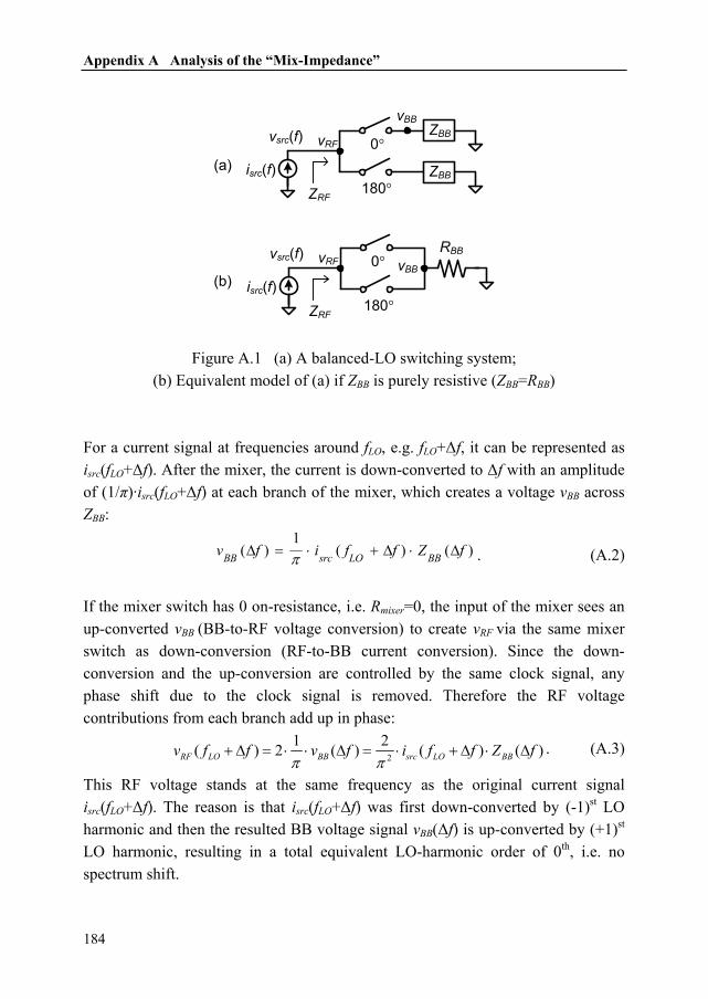
Appendix A Analysis of the “Mix-Impedance”
184
(b)0°
180°isrc(f)
ZRF
vsrc(f)vBB
vRFRBB
ZBB
ZBB
0°
180°(a) isrc(f)
ZRF
vsrc(f)vBB
vRF
Figure A.1 (a) A balanced-LO switching system; (b) Equivalent model of (a) if ZBB is purely resistive (ZBB=RBB)
For a current signal at frequencies around fLO, e.g. fLO+Δf, it can be represented as isrc(fLO+Δf). After the mixer, the current is down-converted to Δf with an amplitude of (1/π)·isrc(fLO+Δf) at each branch of the mixer, which creates a voltage vBB across ZBB:
1( ) ( ) ( )BB src LO BBv f i f f Z fπΔ = ⋅ + Δ ⋅ Δ . (A.2)
If the mixer switch has 0 on-resistance, i.e. Rmixer=0, the input of the mixer sees an up-converted vBB (BB-to-RF voltage conversion) to create vRF via the same mixer switch as down-conversion (RF-to-BB current conversion). Since the down-conversion and the up-conversion are controlled by the same clock signal, any phase shift due to the clock signal is removed. Therefore the RF voltage contributions from each branch add up in phase:
2
1 2( ) 2 ( ) ( ) ( )RF LO BB src LO BBv f f v f i f f Z fπ π
+ Δ = ⋅ ⋅ Δ = ⋅ + Δ ⋅ Δ . (A.3)
This RF voltage stands at the same frequency as the original current signal isrc(fLO+Δf). The reason is that isrc(fLO+Δf) was first down-converted by (-1)st LO harmonic and then the resulted BB voltage signal vBB(Δf) is up-converted by (+1)st LO harmonic, resulting in a total equivalent LO-harmonic order of 0th, i.e. no spectrum shift.
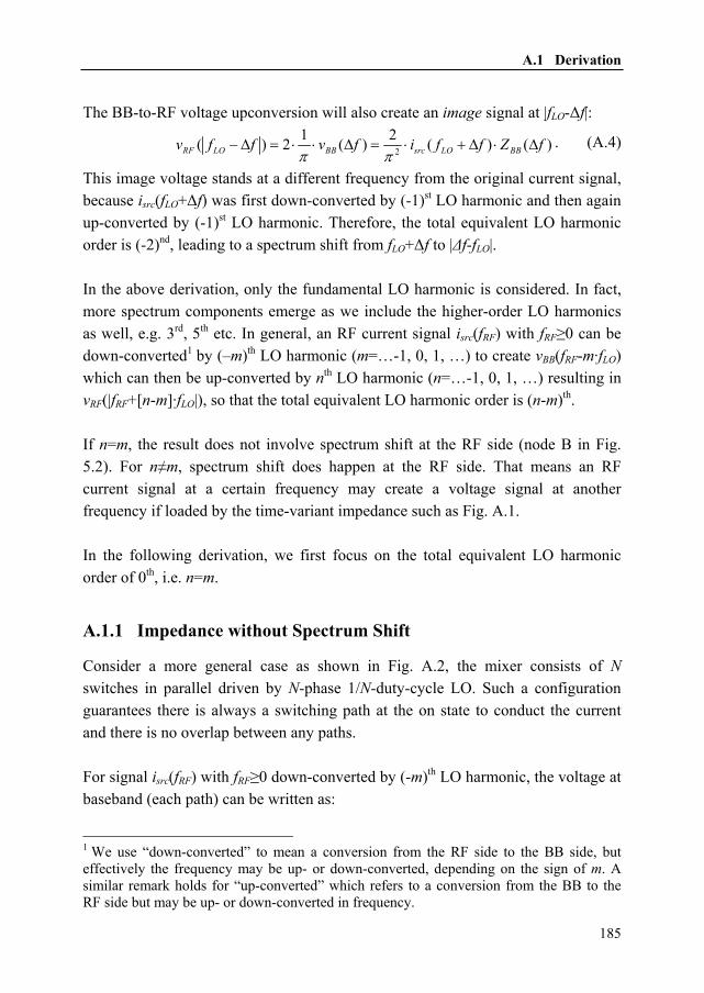
A.1 Derivation
185
The BB-to-RF voltage upconversion will also create an image signal at |fLO-Δf|:
2
1 2( ) 2 ( ) ( ) ( )RF LO BB src LO BBv f f v f i f f Z fπ π
− Δ = ⋅ ⋅ Δ = ⋅ + Δ ⋅ Δ . (A.4)
This image voltage stands at a different frequency from the original current signal, because isrc(fLO+Δf) was first down-converted by (-1)st LO harmonic and then again up-converted by (-1)st LO harmonic. Therefore, the total equivalent LO harmonic order is (-2)nd, leading to a spectrum shift from fLO+Δf to |Δf-fLO|. In the above derivation, only the fundamental LO harmonic is considered. In fact, more spectrum components emerge as we include the higher-order LO harmonics as well, e.g. 3rd, 5th etc. In general, an RF current signal isrc(fRF) with fRF≥0 can be down-converted1 by (–m)th LO harmonic (m=…-1, 0, 1, …) to create vBB(fRF-m·fLO) which can then be up-converted by nth LO harmonic (n=…-1, 0, 1, …) resulting in vRF(|fRF+[n-m]·fLO|), so that the total equivalent LO harmonic order is (n-m)th. If n=m, the result does not involve spectrum shift at the RF side (node B in Fig. 5.2). For n≠m, spectrum shift does happen at the RF side. That means an RF current signal at a certain frequency may create a voltage signal at another frequency if loaded by the time-variant impedance such as Fig. A.1. In the following derivation, we first focus on the total equivalent LO harmonic order of 0th, i.e. n=m.
A.1.1 Impedance without Spectrum Shift
Consider a more general case as shown in Fig. A.2, the mixer consists of N switches in parallel driven by N-phase 1/N-duty-cycle LO. Such a configuration guarantees there is always a switching path at the on state to conduct the current and there is no overlap between any paths. For signal isrc(fRF) with fRF≥0 down-converted by (-m)th LO harmonic, the voltage at baseband (each path) can be written as:
1 We use “down-converted” to mean a conversion from the RF side to the BB side, but effectively the frequency may be up- or down-converted, depending on the sign of m. A similar remark holds for “up-converted” which refers to a conversion from the BB to the RF side but may be up- or down-converted in frequency.
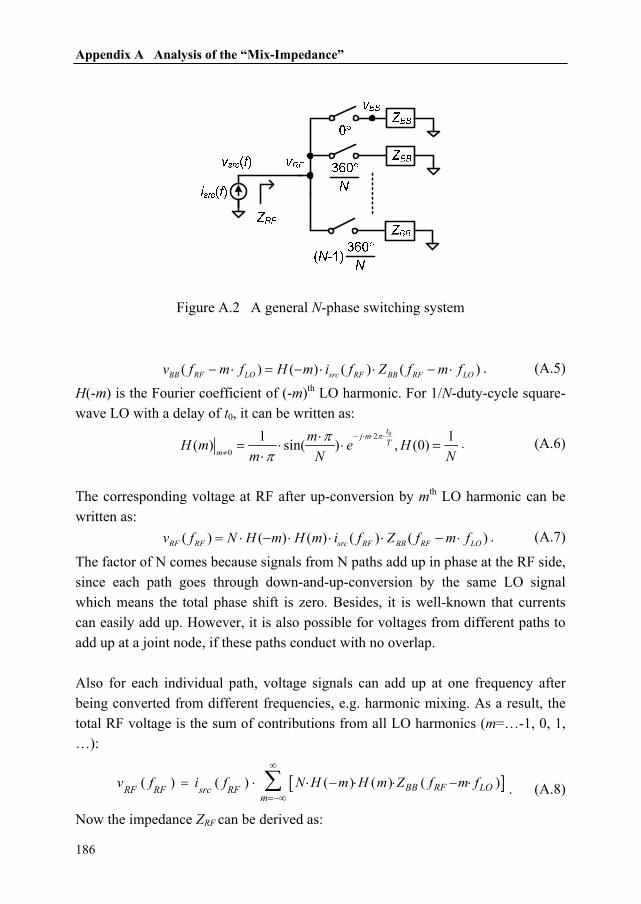
Appendix A Analysis of the “Mix-Impedance”
186
Figure A.2 A general N-phase switching system
( ) ( ) ( ) ( )BB RF LO src RF BB RF LOv f m f H m i f Z f m f− ⋅ = − ⋅ ⋅ − ⋅ . (A.5)
H(-m) is the Fourier coefficient of (-m)th LO harmonic. For 1/N-duty-cycle square-wave LO with a delay of t0, it can be written as:
02
0
1 1( ) sin( ) , (0)tj mT
m
mH m e Hm N N
πππ
− ⋅ ⋅ ⋅
≠
⋅= ⋅ ⋅ =
⋅. (A.6)
The corresponding voltage at RF after up-conversion by mth LO harmonic can be written as:
( ) ( ) ( ) ( ) ( )RF RF src RF BB RF LOv f N H m H m i f Z f m f= ⋅ − ⋅ ⋅ ⋅ − ⋅ . (A.7)
The factor of N comes because signals from N paths add up in phase at the RF side, since each path goes through down-and-up-conversion by the same LO signal which means the total phase shift is zero. Besides, it is well-known that currents can easily add up. However, it is also possible for voltages from different paths to add up at a joint node, if these paths conduct with no overlap. Also for each individual path, voltage signals can add up at one frequency after being converted from different frequencies, e.g. harmonic mixing. As a result, the total RF voltage is the sum of contributions from all LO harmonics (m=…-1, 0, 1, …):
[ ]( ) ( ) ( ) ( ) ( )∞
=−∞= ⋅ ⋅ − ⋅ ⋅ − ⋅∑ BB RF LORF RF src RF
mv f i f N H m H m Z f m f . (A.8)
Now the impedance ZRF can be derived as:

A.1 Derivation
187
[ ]( ) ( )
( ) ( ) ( ) ( )( ) ( )src RF RF RF
BB RF LORF RF src RF src RF m
v f v fZ f N H m H m Z f m fi f i f
∞
=−∞= = = ⋅ − ⋅ ⋅ − ⋅∑ .
(A.9) Suppose N=2, i.e. the case of Fig. A.1, and if ZBB is frequency independent, e.g. ZBB=RBB, applying (A.6) we can write (A.9) as
( )( )
, 02
2 2
2 22
1 2( ) sin ( )2 2
1 2 1 12 1 ( ) ( ) ...2 3 5
m
RF RF BBm
BB BB
mZ f Rm
R R
ππ
π
∞ ≠
=−∞
⋅⎡ ⎤= ⋅ + ⋅⎢ ⎥⋅⎣ ⎦
= ⋅ + ⋅ ⋅ + + + =
∑
⎡ ⎤⎣ ⎦ . (A.10)
It fits exactly what we got from (A.1). Now include the finite switch-on resistance which can be modeled as a single Rmixer in front of the mixer, as shown in Fig. A.3. It generates the same effect as having Rmixer within each of the mixer switches since the on states of any switches do not overlap. Then we have vsrc(fRF):
( ) ( ) ( )src RF RF RF src RF mixerv f v f i f R= + ⋅ . (A.11)
Therefore the impedance is:
[ ]( )
( ) ( ) ( ) ( )( )src RF
BB RF LORF RF mixersrc RF m
v fZ f R N H m H m Z f m fi f
∞
=−∞= = + ⋅ − ⋅ ⋅ − ⋅∑ .
(A.12) If ZBB presents LPF effect to strongly suppress the high-frequency components, e.g. a pole at a much lower frequency than the LO frequency, which is often the case in practice for a down-mixer, (A.12) can be simplified since the contributions of ZBB(fRF-m·fLO) at frequencies around DC are likely to dominate. That means, the impedance ZRF at an RF around mth-LO-harmonic frequency (m=0, 1, 2, 3…), i.e. with an offset frequency Δf from m·fLO, with |Δf|≤fLO/2 and (m·fLO+Δf)≥0, can be written as:
( ) ( ) ( ) ( )RF LO mixer BBZ m f f R N H m H m Z f⋅ + Δ ≈ + ⋅ − ⋅ ⋅ Δ . (A.13)
Substituting (A.6) into (A.13) can obtain (5.3) which does not include the m=0 case for simplicity.
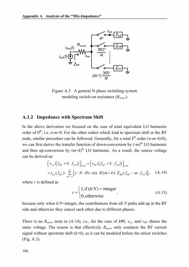
Appendix A Analysis of the “Mix-Impedance”
188
Figure A.3 A general N-phase switching system modeling switch-on resistance (Rmixer)
A.1.2 Impedance with Spectrum Shift
In the above derivation we focused on the case of total equivalent LO harmonic order of 0th, i.e. n-m=0. For the other orders which lead to spectrum shift at the RF node, similar procedure can be followed. Generally, for a total kth order (n-m=k≠0), we can first derive the transfer function of down-conversion by (-m)th LO harmonic and then up-conversion by (m+k)th LO harmonic. As a result, the source voltage can be derived as:
[ ]0 0
( ) ( )
( ) ( ) ( ) ( )
src RF LO RF RF LOk k
src RF BB RF LOm
v f k f v f k f
i f c N H m H m k Z f m f
≠ ≠
∞
=−∞
⎡ ⎤ ⎡ ⎤+ ⋅ = + ⋅⎣ ⎦ ⎣ ⎦
= ⋅ ⋅ ⋅ − ⋅ + ⋅ − ⋅∑ , (A.14)
where c is defined as 1,if ( / ) integer0,otherwise
=⎧= ⎨⎩
k Nc , (A.15)
because only when k/N=integer, the contributions from all N paths add up at the RF side and otherwise they cancel each other due to different phases. There is no Rmixer term in (A.14), i.e., for the case of k≠0, vsrc and vRF shares the same voltage. The reason is that effectively Rmixer only conducts the RF current signal without spectrum shift (k=0), as it can be modeled before the mixer switches (Fig. A.3).

A.1 Derivation
189
From (A.14), we can also see which interference may affect the desired signal due to spectrum shift in a mix-impedance. Suppose the resulted voltage signal falls on top of a desired signal at fLO+∆f, i.e. |fRF+k·fLO|=fLO+∆f. Then we get
[ ] [ ] ( 1) or ( 1) and 0RF LO LO RFf k f f k f f f= − + ⋅ + Δ − − ⋅ − Δ ≥ . (A.16)
If k=-2, we have signal originally at 3fLO+∆f and fLO-∆f to overlap with the desired signal at fLO+∆f, which are the 3rd harmonic interference and the image interference respectively. The impedance resulted from (A.14) involves spectrum shift, i.e. a current signal at fRF creates a voltage signal at |fRF+k·fLO|, and it is named as Zshift to distinguish from ZRF for k=0 case. Zshift can be written as:
[ ]
[ ]
( )0
( )0 ( )
( ) ( ) ( )
RF LOsrc
RF LOshift
src RF
BB RF LOm
v f k fk
Z f k fk i f
c N H m H m k Z f m f∞
=−∞
+ ⋅≠
+ ⋅ =≠
= ⋅ ⋅ − ⋅ + ⋅ − ⋅
⎡ ⎤⎣ ⎦
∑ . (A.17)
A few interesting points can be discovered from (A.17). If N=4, i.e. quadurature mixer driven by 25%-duty-cycle LO, since c=0 if k/4 is not an integer, Zshift is zero for k=-3, -2, -1, 1, 2, 3. That means the 3rd harmonic and image interference will not make trouble according to (A.16). However, the 5th harmonic and the image of 3rd harmonic can still overlap with the desired signal since Zshift for k=-4 is not zero. If N=8, i.e. 8-phase mixer driven by 12.5%-duty-cycle LO, since c=0 if k/8 is not an integer, Zshift is zero for k=-7…-1, 1…7. That means the image interference and 2nd to 6th harmonic interference with their images will not overlap with the desired signal. Intuitively explained, for a 4-phase mixer, since the RF-to-BB current conversion creates quadrature baseband signal, the BB-to-RF voltage conversion driven by four phase LO is equivalent to a single-sideband up-conversion mixer which can eliminate the image signal at the RF side. For more phases, we may apply polyphase multipath principle [1]. For N mixer switches in parallel driven by N-phase LO, the RF-to-BB current conversion creates N-phase baseband signal. Then

Appendix A Analysis of the “Mix-Impedance”
190
the BB-to-RF voltage conversion is equivalent to a polyphase multipath up-converter, which adds all N paths in phase at RF and may cancel up to (N-2)th LO harmonics [2].
A.2 Simulation To verify the theory presented above, we may compare the simulation results with the calculated results via (A.12) and (A.17), which is general for different LO waveforms. For a specific square-wave LO with 1/N duty-cycle, substituting (A.6) into (A.12) and (A.17) respectively, we get:
, 0 22 2
1 1( ) ( ) sin ( ) ( )2
m
RF RF mixer BB RF BB RF LOm
mZ f R Z f N Z f m fm N
ππ
∞ ≠
=−∞
⋅⎡ ⎤= + ⋅ + ⋅ ⋅ ⋅ − ⋅∑ ⎢ ⎥⋅⎣ ⎦,
(A.18) and
0
0
0, 2
2...
( )
[ ]sin( ) sin( ) ( )( )
shift RF LO k
tm m k j kT
BB RF LOm
Z f k f
c N m m k e Z f m fm m k N N
ππ ππ
≠
≠ ≠− − ⋅ ⋅ ⋅
=−∞ ∞
⎡ ⎤+ ⋅ =⎣ ⎦
⎡ ⎤⋅ ⋅ + ⋅⋅ ⋅ ⋅ ⋅ − ⋅∑ ⎢ ⎥⋅ + ⋅⎣ ⎦
.
(A.19) We can see that ZRF is independent of the initial phase (t0) of the LO, while Zshift is dependent. If only to consider the magnitude, t0 makes no difference, but it does change the real and imaginary parts of Zshift. A simulation setup same as Fig. A.2 has been built up with ideal components (current source, switches with internal Rmixer, and baseband impedance) to eliminate the effect of parasitic elements which are not considered in the equations. The comparison is carried out with N=8, i.e. an 8-phase system, and a maximum m=51, i.e. considering up to the 51st LO harmonic. The LO frequency (fLO) is at 1GHz with 1/8 duty-cycle and the RF range (fRF) is from DC to 5GHz. The LO harmonic strength is determined by the LO waveform which is affected by the rise and fall time. To be precise, a small rise and fall time of 1fs is used to match, as close as possible, the amplitude of the Fourier coefficients described by (A.6). Two different LO initial phases of t0=0 or t0=T/9 are tested to check the effect of initial LO delay. The baseband impedance consists of a resistor RBB=1kΩ and a capacitor CBB=10pF in parallel to ground, corresponding to a pole at 16MHz, and the mixer

A.2 Simulation
191
0 1 2 3 4 5-20
0
20
40
60
calculatedsimulated
0 1 2 3 4 50
40
80
120
160
0 1 2 3 4 5-100
-60-202060
100
calculatedsimulated
(a)
(b)
Figure A.4 Calculated via (A.18) and simulated ZRF with Rmixer=1mΩ:
(a) magnitude in dB; (b) real and imaginary parts
switch-on resistance is either Rmixer=50Ω or Rmixer=1mΩ to demonstrate different scenarios with or without mixer resistance. First we look at (A.18). With Rmixer=1mΩ, the magnitudes of simulated and calculated ZRF (k=0) are plot in Fig. A.4 (a), and they show an exact match. Since impedance may consist of real and imaginary parts, we compared these two separately as well. Fig. A.4 (b) gives both simulated and calculated results which match very well too. Fig. A.5 shows the case for Rmixer=50Ω where the real part shows an offset value of Rmixer as expected. The same results hold for different t0

Appendix A Analysis of the “Mix-Impedance”
192
0 1 2 3 4 550
90
130
170
210
0 1 2 3 4 5-100
-60-202060
100
calculatedsimulated
Figure A.5 Calculated via (A.18) and simulated ZRF:
real and imaginary parts with Rmixer=50Ω
0 1 2 3 4 5-20
-10
0
10
20
30
40
50
calculatedsimulated
0 1 2 3 4 532
34
36
38
40
42
44
46
calculatedsimulated
(a)
(b)
Figure A.6 Calculated via simplified equation (A.13) and simulated ZRF:
magnitude in dB with (a) Rmixer=1mΩ (b) Rmixer=50Ω

A.2 Simulation
193
0 2 4 6 8 10 12-180
-160
-140
-120
-100
-80
-60
Figure A.7 Simulated Zshift: magnitude in dB with k=-7…-1, 1…7
values. These results prove our derivation for ZRF, via (A.12) in general and (A.18) for the specific LO waveform. To check the accuracy of the simplified equation (A.13), or (5.3) without considering spectrum around DC, we plotted in Fig. A.6, the simulated magnitude and calculated magnitude via (A.13). If Rmixer=1mΩ as in Fig. A.6 (a), the approximation is good around peak values but less accurate when ZRF drops low. Nevertheless, in practice, Rmixer is often in the order of tens of Ohms. For our design (Fig. 5.4), Rmixer=50Ω, and Fig. A.6 (b) shows that then the approximation is pretty good for all values since Rmixer now dominates low ZRF values. Then, we look at (A.19). In simulation, we checked k=-7…-1, 1…7, which should give Zshift=0 since c=0 according to (A.15). The simulated Zshift magnitudes are shown in Fig. A.7, independent of Rmixer. All results are below -70dBΩ which means a negligible impedance, confirming the theory.

Appendix A Analysis of the “Mix-Impedance”
194
8 9 10 11 12 13-40
-30
-20
-10
0
10
20
30
calculatedsimulated
8 9 10 11 12 13-40
-20
0
20
calculatedsimulated
8 9 10 11 12 13
-10
0
10
(a)
(b)
Figure A.8 Calculated via (A.19) and simulated Zshift with k=8 and t0=0: (a) magnitude in dB; (b) real and imaginary parts
Further, we compare a non-canceled Zshift with k=8, so that c=1 according to (A.15). The simulated and calculated Zshift in magnitude and real/imaginary parts are shown in Fig. A.8 (a) and (b), respectively, for the t0=0 case. A very good fit is found again. We also checked t0=T/9, and the comparisons for magnitude and real/imaginary parts are plotted in Fig. A.9 (a) and (b), showing no difference. However, it shows the effect of t0, which does not affect magnitude but does change the real and imaginary parts compared to Fig. A.8. All these simulation results are independent of Rmixer. Therefore, we may conclude that the derived Zshift, via (A.17) in general and (A.19) for the specific LO waveform, is verified.

A.3 References
195
8 9 10 11 12 13-40
-30
-20
-10
0
10
20
30
calculatedsimulated
8 9 10 11 12 13
-20
-10
0
10
calculatedsimulated
8 9 10 11 12 13
-20
-10
0
10
(a)
(b)
Figure A.9 Calculated via (A.19) and simulated Zshift with k=8 and t0=T/9: (a) magnitude in dB; (b) real and imaginary parts
A.3 References [1] E. Mensink, E.A.M. Klumperink, B. Nauta, "Distortion cancellation by
polyphase multipath circuits," IEEE Trans. Circuits and Systems I: Regular Papers, vol.52, no.9, pp. 1785-1794, Sept. 2005
[2] R. Shrestha, E.A.M. Klumperink, E. Mensink, G.J.M. Wienk, B. Nauta, "A Polyphase Multipath Technique for Software-Defined Radio Transmitters," IEEE J. Solid-State Circuits, vol.41, no.12, pp.2681-2692, Dec. 2006

Appendix A Analysis of the “Mix-Impedance”
196
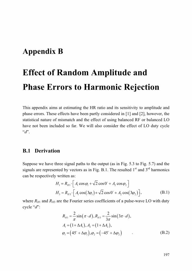
197
Appendix B Effect of Random Amplitude and
Phase Errors to Harmonic Rejection This appendix aims at estimating the HR ratio and its sensitivity to amplitude and phase errors. These effects have been partly considered in [1] and [2], however, the statistical nature of mismatch and the effect of using balanced RF or balanced LO have not been included so far. We will also consider the effect of LO duty cycle “d”.
B.1 Derivation Suppose we have three signal paths to the output (as in Fig. 5.3 to Fig. 5.7) and the signals are represented by vectors as in Fig. B.1. The resulted 1st and 3rd harmonics can be respectively written as:
( ) ( )1 1 1 1 2 2
3 3 1 1 2 2
cos 2 cos0 cos
cos 3 2 cos0 cos 3
H
H
H R A A
H R A A
ϕ ϕ
ϕ ϕ
⎡ ⎤= ⋅ + +⎣ ⎦⎡ ⎤= ⋅ + +⎣ ⎦
o
o , (B.1)
where RH1 and RH3 are the Fourier series coefficients of a pulse-wave LO with duty cycle “d”:
( ) ( )
( ) ( )( ) ( )
1 3
1 1 2 2
1 1 2 2
2 2sin , sin 3 ,3
1 , 1 ,
45 , 45
H HR d R d
A A A A
π ππ π
ϕ ϕ ϕ ϕ
= ⋅ = ⋅
= + Δ = + Δ
= + Δ = − + Δo o . (B.2)

Appendix B Effect of Radom Amplitude and Phase Errors to Harmonic Rejection
198
3rd harmonic 45°
1
1 √2
3·Δφ1
3·Δφ2
1+ΔA1
1+ΔA2
1st harmonic√245°
1
1
Δφ11+ΔA1
Δφ2
1+ΔA2
Figure B.1 Vector diagram modeling amplitude and phase errors for 8-phase harmonic rejection
If ΔA1, ΔA2, Δφ1, Δφ2 are small and uncorrelated, we can approximate the variance in H3 as:
2 2 2 22 2 2 2 2 23 3 3 3
3 3 1 2 1 21 2 1 2
H H A AH H H HRA A ϕ ϕσ σ σ σ σ
ϕ ϕ
⎡ ⎤⎛ ⎞ ⎛ ⎞ ⎛ ⎞ ⎛ ⎞∂ ∂ ∂ ∂⎢ ⎥≈ ⋅ ⋅ + ⋅ + ⋅ + ⋅⎜ ⎟ ⎜ ⎟ ⎜ ⎟ ⎜ ⎟∂ ∂ ∂ ∂⎢ ⎥⎝ ⎠ ⎝ ⎠ ⎝ ⎠ ⎝ ⎠⎣ ⎦
. (B.3)
If σA1=σA2=σA and σφ1=σφ2=σφ, then:
( ) ( )2 2 2 2 2 2 2 2 23 3 32cos 3 45 18sin 3 45 9H H A H AR Rϕ ϕσ σ σ σ σ⎡ ⎤ ⎡ ⎤≈ ⋅ ⋅ ⋅ + ⋅ ⋅ = ⋅ +⎣ ⎦⎣ ⎦
o o . (B.4)
Since H1≈2√2·RH1, taking the ratio, we obtain: 22 2 2 22 2
332 2 2
1 1
9 sin (3 )8 sin ( ) 6 2 2 2
H AH A
H
R dH R d
ϕ ϕσ σ σσ σππ
⎡ ⎤⎡ ⎤⋅ +⎛ ⎞ ⎛ ⎞⋅ ⎛ ⎞⎣ ⎦≈ = +⎢ ⎥⎜ ⎟ ⎜ ⎟⎜ ⎟⋅ ⎝ ⎠⎢ ⎥⎝ ⎠⎝ ⎠ ⎣ ⎦. (B.5)
Please note that σA is the standard deviation of amplitude error in percentage and σφ
is the standard deviation of phase error in radians. For a double-balanced HR mixer, which creates the output during one half period from 0 to T/2 with the positive-sign RF-LNTA path then the other half from T/2 to T with the negative-sign RF-LNTA path, the 1st harmonic adds up in amplitude while the 3rd harmonic adds up in power (as the error is uncorrelated between twohalf periods for both amplitude and phase). Therefore, the ratio is improved by 3dB for a double-balanced HR mixer compared to (B.5), i.e.

B.2 Simulation
199
222 232 2
1
sin (3 )sin ( ) 12 4
H A
diff
dH d
ϕσσ σππ
⎡ ⎤⎛ ⎞ ⎛ ⎞⋅ ⎛ ⎞≈ +⎢ ⎥⎜ ⎟ ⎜ ⎟⎜ ⎟⋅ ⎝ ⎠⎢ ⎥⎝ ⎠⎝ ⎠ ⎣ ⎦. (B.6)
If the duty cycle of the LO is 50% or 25%, i.e. d=0.5 or 0.25, we get
( ) ( ) ( )22 223 1
,50%12 4H A
diffH ϕσ σ σ≈ + . (B.7)
If there is no amplitude error, 50% or 25% duty cycle results in a 3σ-HR3 of 70dB if σφ=0.024°. If the duty cycle is 1/8, i.e. d=0.125, as in our case, we get:
( ) ( ) ( )22 223 1
,12.5%5.8 12 4H A
diffH ϕσ σ σ⎡ ⎤≈ ⋅ +⎢ ⎥⎣ ⎦
. (B.8)
Without amplitude error, the 3σ-HR3 is now 62dB. A similar derivation for 5th order HR of a double-balanced HR mixer renders:
( )( )
222252 2
1
sin 5sin 20 4
H A
diff
dH d
ϕσπσ σπ
⎡ ⎤⋅⎛ ⎞ ⎛ ⎞⎛ ⎞≈ ⋅ +⎢ ⎥⎜ ⎟ ⎜ ⎟⎜ ⎟⋅ ⎝ ⎠⎢ ⎥⎝ ⎠⎝ ⎠ ⎣ ⎦. (B.9)
where the phase term σφ would have been multiplied by 5 in (B.5) due to the 5-times phase shift of H5 compared to H1. Nevertheless, without amplitude errors, this leads to the same numerical result (σφ=0.024°): a 3σ-HR5 of 62dB for 1/8 duty cycle LO.
B.2 Simulation Fig. B.2 plots the 3rd-order HR (HR3) and 5th-order HR (HR5) versus amplitude and phase errors with 1/8 duty cycle, based on (B.6) and (B.9) respectively. In the figure, Psigma means σφ and Asigma means σA. The HR results in dB correspond to 3-sigma errors. We can see that when σA≥0.5%, phase error hardly affects HR ratio. While if σA≤0.1%, phase error can easily dominate with σφ ≥0.02°.

Appendix B Effect of Radom Amplitude and Phase Errors to Harmonic Rejection
200
0 0.01 0.02 0.03 0.04 0.0540
60
80
100
Asigma=0Asigma=0.1%Asigma=0.5%
0 0.01 0.02 0.03 0.04 0.0540
60
80
100
Asigma=0Asigma=0.1%Asigma=0.5%
Figure B.2 Effect of amplitude error (Asigma= σA) and phase error (Psigma=σφ) to HR with 1/8 duty-cycle LO
0 0.2 0.4 0.6 0.8 150
60
70
80
90
100
Duty Cycle
HR
3-s
igm
a (d
B)
HR3HR5
Figure B.3 Effect of duty cycle (d) to HR, with σA=0.1% and σφ=0.03°

B.3 References
201
Fig. B.3 plots the 3-sigma HR3 and HR5 versus duty cycle (d) with σA=0.1% and σφ=0.03°. We can see that the duty cycle effect is symmetrical around d=0.5 as can be understood, and presents a few narrow peaks for both HR3 and HR5. These HR peaks are due to the facts that sin(3π·d) in (B.6) is close to 0 when d is around 1/3 and 2/3, and sin(5π·d) in (B.9) is close to 0 when d is around 1/5, 2/5, 3/5 and 4/5. For the convenience of illustration, the upper limit of the peaking values in the figure is set to 100dB while in theory an exact 0 value for sin(3π·d) or sin(5π·d) can lead to infinite HR ratio. From Fig. B.3 we can also see that around d=0.5, the 3rd and 5th HR ratios are generally larger than the cases when d approaches 0 or 1. This is because the relative strength of harmonic components in a square-wave clock can vary for different duty cycles. B.3 References [1] J.A. Weldon, R.S. Narayanaswami, J.C. Rudell, et. al., "A 1.75-GHz highly
integrated narrow-band CMOS transmitter with harmonic-rejection mixers," IEEE J. Solid-State Circuits, vol.36, no.12, pp.2003-2015, Dec. 2001
[2] R. Bagheri, A. Mirzaei, S. Chehrazi, et. al., "An 800-MHz–6-GHz Software-Defined Wireless Receiver in 90-nm CMOS", IEEE J. Solid-State Circuits, vol.41, no.12, pp.2860-2876, Dec. 2006

Appendix B Effect of Radom Amplitude and Phase Errors to Harmonic Rejection
202

203
Acknowledgements Ph.D. work is usually regarded as independent research, but it often cannot be done without the support from many others. Here I wish to acknowledge a number of people who contributed directly or indirectly to this work. First of all, I would like to thank my daily supervisor Eric Klumperink and my promotor Bram Nauta. The devoted guidance from Eric is invaluable. His efforts and enthusiasms are indispensable to this work. Bram picked me up from Sweden and led my way into the Integrated Circuit Design (ICD) group. His insights and encouragements are essential to this work. My thanks go to Freeband Communication for funding and NXP Semiconductors for chip fabrication. I would like to thank all members of the WiComm project within Freeband, for the interesting meetings we had together. Within NXP, especially I am grateful to Hans Brekelmans, Domine Leenaerts, and Raf Roovers, for providing the chips and useful technical discussions. Thanks for the technical support from Gerard and Henk. Gerard really helped a lot on PCB, measurement, and EDA tools as well as layout assistance. Henk maintained the lab in a good order and solved many practical problems with patience. They can almost always come up with some solutions to all kinds of problems encountered during measurement. I also want to thank the help from Gerdien and Frederik. Gerdien is so kind and she helped on many administrative issues through all phases of the work. Frederik is a responsible computer expert who settled many computer and network related issues. I also thank other people in the PAO and the ICT departments for their help. I would like to thank Niels for the four-year cooperation which made the work more enjoyable and fruitful. His good understanding and sense of humor made our

204
discussions more pleasant. I also want to thank Professor Carlos Saavedra from Queen’s University at Canada, for the cooperation during his half-year visit to the ICD group. My thanks go to Vincent and Roel, who took part in the discussions in the early phase of this project. They have worked on the first-generation software-defined radio in Twente, which gained valuable experience for this work. My thanks go to all former and current members in the ICD group for forming such a wonderful group and helping each other. I would like to thank my former and current officemates: Simon and Jan Rutger; Ramen and Feng; Dlovan and Amir. They are nice people to work with and we had fun together. I also want to thank the members of the Semiconductor Components group on the same floor. Thanks for the many cakes and making an active atmosphere in the corridor. Especially my thanks go to Annemiek for her generous help. Thanks for the friendship with Wei and Xiang from the ICD group and all my other Chinese friends in the Netherlands. They made the life here more enjoyable. I am also grateful to Libo in Germany for keeping the distant contact over years. Thanks to all my former and current roommates. They made the living here not lonely. Thanks to Xiaocheng who made the apartment more fun. I also would like to thank people I met in Lund, Sweden. Thanks to Professor Jiren Yuan and Professor Henrik Sjöland for their teaching on analog and RF knowledge and their recommendations. Thanks to Dr. Gang Xu who encouraged me to contact Twente which was the starting point of the long journey of this work. My thanks go to everyone who ever helped me. Most especially, I want to thank all my family members. I am indebted to my parents for their unconditional support. I thank Rong for her love, support, and understanding. Zhiyu Ru Enschede, October 2009

205
Samenvatting Er is een toenemende vraag naar draadloze communicatie en er zijn in de loop van de tijd diverse communicatiestandaarden ontwikkeld voor dit doel, bv. voor GSM, Bluetooth, Wi-Fi, etc. Vanwege het gebruiksgemak wil gebruikers graag een universele radio die overal werkt voor alle standaarden. Een "software-defined radio" (SDR) met programmeerbare radio functionaliteit kan aan deze vraag voldoen. Er zijn echter een aantal technische uitdagingen om een SDR-ontvanger praktisch realiseerbaar te maken. Dit proefschrift richt zich op radio-frequentie (RF) frequentie translatie technieken, met nadruk op twee belangrijke SDR-ontvanger uitdagingen: de robuustheid voor out-of-band interferentie (OBI) en de compatibiliteit met CMOS en system-on-chip integratie. Dit proefschrift bestudeert de principes en prestatiebeperkingen van bestaande frequentie translatie technieken en stelt nieuwe circuit- en systeemtechnieken voor die betere SDR-ontvangers mogelijk maken. Fundamentele verschillen tussen diverse frequentie translatie technieken worden aan het licht gebracht door middel van een classificatie van mixer and sampler technieken. Dit leidt tot de definitie van een nieuwe discrete-time (DT) mixer techniek. Verder worden RF-mixen en RF-samplen vergeleken met betrekking tot hun geschiktheid voor SDR. RF-samplen lijkt daarbij in het voordeel qua compatibiliteit met CMOS en system-on-chip integratie. Bestaande RF sampling ontvangers zijn echter smalbandig en zijn niet direct geschikt voor breedbandige SDR toepassingen. Om dit probleem aan te pakken wordt een nieuwe discrete-time mixer techniek voorgesteld, die een mixer operatie in het DT-domein uitvoert na RF-sampling. Deze techniek maakt RF-samplen meer geschikt voor breedbandige SDR-ontvangers doordat DT-mixen zowel een breedbandige faseverschuiving als een breedbandige harmonische rejectie (HR) geeft. DT-mixen kan eenvoudig worden

206
gerealiseerd met behulp van de-multiplexen van samples. De praktische werking van het concept wordt gedemonstreerd door een 200-900MHz DT-mixer ontwerp met 8-voudige RF-oversampling en 2e-tot-6e HR, geïmplementeerd op een chip in 65nm CMOS technologie. Om hiermee een complete RF-ontvanger te realiseren, is een afstembare LC filter en een gelineariseerde ruisarme voorversterker op de chip toegevoegd, voorafgaand aan de DT-mixer. Het LC-filter gebruikt één externe spoel en schakelbare condensatoren op chip voor de frequentie afstemming. De ruisarme voorversterker bestaat uit een cascade van CMOS-inverters, gelineariseerd via een “spannings-spiegel” concept. De totale RF-sampling ontvanger heeft een minimale Noise Figure van 0.8dB, terwijl deze de HR met 30dB verbetert. Om RF mixers beter bestand te maken tegen OBI worden voorts twee technieken voorgesteld: een techniek die de “out-of-band lineariteit” verbetert en een andere die de HR robuust maakt voor bij productie optredende component ongelijkheden. Daarbij wordt spanningsversterking niet op hoge frequenties gerealiseerd, maar uitgesteld tot na de conversie naar basisband, alwaar laagdoorlaat filtering in combinatie met versterking plaatsvindt om de OBI te onderdrukken. De lage spanningsversterking bij hoge frequenties wordt bereikt via een "mix-impedantie", die kwantitatief geanalyseerd wordt. Om de HR aanzienlijk te verbeteren en ongevoelig te maken voor amplitude fouten, wordt een 2-traps polyfase HR-techniek voorgesteld. Om tevens een goede fasenauwkeurigheid te bereiken, is een nauwkeurige frequentiedeler ontworpen. De effecten van random amplitude en fase fouten op de HR worden ook geanalyseerd. Om aan te tonen dat de concepten werken, is in 65nm CMOS technologie een ontvanger geïmplementeerd die een “in-band” IIP3 van +3.5dBm heeft en +16dBm “out-of-band IIP3”. Meer dan 60dB HR is gemeten over 40 willekeurig gekozen chips. De multifase klok generator werkt tot 0.9GHz, terwijl de -3dB RF-bandbreedte meer dan 6GHz is.

207
Publications Journal Papers Z. Ru, N.A. Moseley, E.A.M. Klumperink, B. Nauta, “Digitally-Enhanced Software-Defined Radio Receiver Robust to Out-of-Band Interference”, accepted by IEEE Journal of Solid-State Circuits, Dec. 2009 Z. Ru, E.A.M. Klumperink, B. Nauta, “Discrete-Time Mixing Receiver Architecture for RF-Sampling Software-Defined Radio”, submitted to IEEE Journal of Solid-State Circuits Z. Ru, E.A.M. Klumperink, C.E. Saavedra, B. Nauta, "A 300-800MHz Tunable Filter and Linearized LNA applied in a Low-Noise Harmonic-Rejection RF-Sampling Receiver", submitted to IEEE Journal of Solid-State Circuits, Special Issue on RFIC Symposium 2009
Conference Papers Z. Ru, E.A.M. Klumperink, B. Nauta, "On the Suitability of Discrete-Time Receivers for Software-Defined Radio," IEEE ISCAS, Proceedings of, pp.2522-2525, May 2007 Z. Ru, E.A.M. Klumperink, B. Nauta, "A Discrete-Time Mixing Receiver Architecture with Wideband Harmonic Rejection", IEEE ISSCC, Digest of Technical Papers, pp.322-323. Feb. 2008

208
Z. Ru, E.A.M. Klumperink, G.J.M. Wienk, B. Nauta, "A Software-Defined Radio Receiver Architecture Robust to Out-of-Band Interference," IEEE ISSCC, Digest of Technical Papers, pp.230-231, Feb. 2009 Z. Ru, E.A.M. Klumperink, C.E. Saavedra, B. Nauta, "A Tunable 300–800MHz RF-Sampling Receiver achieving 60dB Harmonic Rejection and 0.8dB Minimum NF in 65nm CMOS," IEEE RFIC Symposium, Proceedings of, pp.21-24, June 2009 N.A. Moseley, Z. Ru, E.A.M. Klumperink, B. Nauta, "A 400-to-900 MHz Receiver with Dual-Domain Harmonic Rejection Exploiting Adaptive Interference Cancellation", IEEE ISSCC, Digest of Technical Papers, pp.232-233, Feb. 2009 M.C.M. Soer, E.A.M. Klumperink, Z. Ru, F.E. van Vliet, B. Nauta, "A 0.2-to-2.0GHz 65nm CMOS Receiver without LNA achieving >11dBm IIP3 and <6.5 dB NF," IEEE ISSCC, Digest of Technical Papers, pp.222-223, Feb. 2009
Patents Z. Ru, E.A.M. Klumperink, B. Nauta, H. Brekelmans, “Polyphase Harmonic Rejection Mixer”, Patent EP 091000095.0., Filed, Feb. 2009

209
About the Author Zhiyu Ru received the B.Eng. degree from Southeast University, Nanjing, China, in 2002 and the M.Sc. degree from Lund University, Lund, Sweden, in 2004, both in electrical engineering. In 2003, he was a design engineer with Z-Com working for WLAN products. In 2004, he did a 6-month internship with Ericsson Mobile Platforms (now ST-Ericsson) working on DVB-T receiver systems. From 2005, he has been with University of Twente, Enschede, Netherlands, working towards the Ph.D. degree on the subject of software-defined radio receivers in CMOS.