Embed Size (px)
Citation preview

60

potentials of tens of volts or higher to switch, requiring more printed battery cells to power them than are feasible to fabricate. The organic electrochemical transistor, or OECT (White et al., 1984), is a more feasible option that we consider here. Unlike OFETs that rely on electrostatic gating, OECTs rely on electrochemical doping/de-doping to switch the transistor on and off. These devices have low (< 1V) operating voltages, their performance does not depend heavily on their dimensions, and the entire transistor can be fabricated under ambient conditions. We have successfully produced functional OECTs using one of our multi-material freeform fabrication systems. Their electrical performance, which we have characterized, is qualitatively similar to the reported performance of similar OECTs in the literature (Nilsson et al., 2005). Having produced these working devices on glass substrates, we have identified several printable substrate materials for the next generation of devices, and are in the process of characterizing them. Using the information gained from these efforts, we have added inkjet deposition capability to one of our SFF systems, improving the machine’s ability to produce high-resolution thin films. These developments will enable us to produce more compact transistors with higher performance and better reproducibility, which can be integrated into larger fully-printed electromechanical devices.
Background Most transistors used in electronic devices today are fabricated on single-crystal silicon wafers, have micron and sub-micron sized features, and require large and very costly equipment in clean-room environments for processing. The most promising materials for printable transistors are organic semiconductors, which are often solution-processable and do not demand such stringent environmental constraints during processing. While spin-coating and photolithography are used to define the features of many organic transistors (Ziemelis, 1998), transistors and even entire circuits fully printed with ink jet or screen printing mechanisms have also been developed (Paul et al., 2003; Katz, 2004; Berggren et al., 2007). These advances have opened up the possibility of printing working transistors on a low cost freeform fabrication system, or “fabber,” which can also print the wires, batteries, actuators, and structural components required to fabricate an entire working electromechanical device. Working with such a versatile system, however, means handling various other constraints. All materials must be “addition-processable” – this usually implies deposition of liquids, but may also include vapor deposition, as with Optomec’s M3D process, (Hedges et al., 2005) or controlled solidification (as in stereolithography). This requirement includes the active materials in the transistor as well as electrically conductive materials used for electrical contacts and wires. We also need to develop a printable, electrically insulating substrate for our transistors, allowing them to be integrated into larger fully-printed devices. All of these materials should be processable in ambient conditions; we can anneal while printing with our research platform, but many materials require treatment in an oxygen-free environment, or release noxious fumes during drying or annealing. Because of the physical limitations of our current syringe-based deposition process, the transistors cannot have any lateral dimensions smaller than 250 micrometers. A drop-cast or printed film of material, in theory, can be made arbitrarily thin, as a very thin material could be produced by printing that material from a very dilute solution, but it is difficult to ensure the robustness and uniformity of such a film. Finally, if we wish to incorporate these transistors into fully-printed electromechanical devices, the transistors need to run at voltages and currents low enough that the transistors can be powered with a reasonable number of printable battery cells.
61
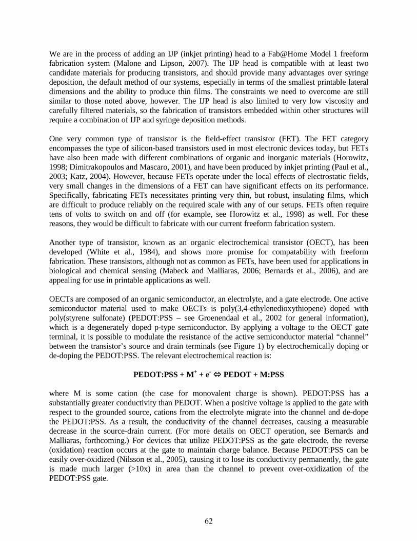
We are in the process of adding an IJP (inkjet printing) head to a Fab@Home Model 1 freeform fabrication system (Malone and Lipson, 2007). The IJP head is compatible with at least two candidate materials for producing transistors, and should provide many advantages over syringe deposition, the default method of our systems, especially in terms of the smallest printable lateral dimensions and the ability to produce thin films. The constraints we need to overcome are still similar to those noted above, however. The IJP head is also limited to very low viscosity and carefully filtered materials, so the fabrication of transistors embedded within other structures will require a combination of IJP and syringe deposition methods. One very common type of transistor is the field-effect transistor (FET). The FET category encompasses the type of silicon-based transistors used in most electronic devices today, but FETs have also been made with different combinations of organic and inorganic materials (Horowitz, 1998; Dimitrakopoulos and Mascaro, 2001), and have been produced by inkjet printing (Paul et al., 2003; Katz, 2004). However, because FETs operate under the local effects of electrostatic fields, very small changes in the dimensions of a FET can have significant effects on its performance. Specifically, fabricating FETs necessitates printing very thin, but robust, insulating films, which are difficult to produce reliably on the required scale with any of our setups. FETs often require tens of volts to switch on and off (for example, see Horowitz et al., 1998) as well. For these reasons, they would be difficult to fabricate with our current freeform fabrication system. Another type of transistor, known as an organic electrochemical transistor (OECT), has been developed (White et al., 1984), and shows more promise for compatability with freeform fabrication. These transistors, although not as common as FETs, have been used for applications in biological and chemical sensing (Mabeck and Malliaras, 2006; Bernards et al., 2006), and are appealing for use in printable applications as well. OECTs are composed of an organic semiconductor, an electrolyte, and a gate electrode. One active semiconductor material used to make OECTs is poly(3,4-ethylenedioxythiopene) doped with poly(styrene sulfonate) (PEDOT:PSS – see Groenendaal et al., 2002 for general information), which is a degenerately doped p-type semiconductor. By applying a voltage to the OECT gate terminal, it is possible to modulate the resistance of the active semiconductor material “channel” between the transistor’s source and drain terminals (see Figure 1) by electrochemically doping or de-doping the PEDOT:PSS. The relevant electrochemical reaction is:
PEDOT:PSS + M+ + e- PEDOT + M:PSS where M is some cation (the case for monovalent charge is shown). PEDOT:PSS has a substantially greater conductivity than PEDOT. When a positive voltage is applied to the gate with respect to the grounded source, cations from the electrolyte migrate into the channel and de-dope the PEDOT:PSS. As a result, the conductivity of the channel decreases, causing a measurable decrease in the source-drain current. (For more details on OECT operation, see Bernards and Malliaras, forthcoming.) For devices that utilize PEDOT:PSS as the gate electrode, the reverse (oxidation) reaction occurs at the gate to maintain charge balance. Because PEDOT:PSS can be easily over-oxidized (Nilsson et al., 2005), causing it to lose its conductivity permanently, the gate is made much larger (>10x) in area than the channel to prevent over-oxidization of the PEDOT:PSS gate.
62
M+
M+
M+
M+
M+
M+
M+
M+
+
–
VG
G
SD
Figure 1 – A schematic of an OECT designed to be printed laterally. The blue material represents an electrochemically-switchable material, which the yellow material represents an electrolyte (containing M+ cations). The resulting I-V behavior from PEDOT:PSS OECTs was published by Nilsson et al. in 2002 and 2005. When a negative potential is applied to the drain, current saturation is observed as the magnitude of the drain potential increases, which is desirable if the transistor is to be used as part of an amplifier. A positive potential applied at the gate decreases the amount of current that flows between the source and drain. The behavior exhibited by transistors biased with negative drain and positive gate potentials looks qualitatively similar to the behavior expected from depletion mode field-effect devices. These OECTs require less than 1V between the gate and source to switch from “on” to “off” as well, meaning that they could be powered with a single printed battery cell. It is not difficult to find mutually insoluble and compatible materials to make OECTs. They can be printed laterally (as in Figure 1); the gate, source, and drain can all be printed simultaneously on a single layer with a single material. Fewer layers mean fewer solvent compatibility issues, as well as a device that is easy to print. PEDOT:PSS is available commercially as an aqueous dispersion, but a dried film of PEDOT:PSS is relatively robust in water. This property opens the possibility of using an aqueous solution as the electrolyte material. Additionally, we have previously printed conducting “wires” using commercial colloidal silver ink and also by depositing molten Pb-Sn alloy (Malone et al., 2004); the silver ink is also appropriate for the metallic contacts needed to connect the OECTs to other devices, as it employs a solvent that does not dissolve the PEDOT:PSS. This gives a full set of materials suitable for ECT production that are easy for us to work with. OECTs are also less sensitive to size than FETs. They rely on bulk electrochemical reactions in the active material to switch on and off, making distances less important than is the case with field-effect transistors. None of the printed layers of OECTs need to be extremely thin, and OECTs with key features on the order of millimeters are functional, as we report here and as is reported elsewhere (Robinson et al., 2006). These same properties of OECTs also make them significantly slower than FETs, but this is acceptable for our current needs. Since we are limited in the size and reproducibility of the lateral dimensions and thicknesses of the materials we print, OECTs are a good starting point for freefrom fabricated transistors.
63
PEDOT:PSS-based devices are, additionally, very versatile. PEDOT:PSS transistors can be made to mimic the behavior of either “n-type” or “p-type” FETs (“n” and “p” designate the type of charge carriers in the FET semiconductor; both types are used in logic circuitry) (Chen, 2005). This is an improvement over OFETs, since organic n-type semiconductors tend to be unstable. PEDOT:PSS-based electrochemical devices have been used to make rectifiers (Chen, 2006), logic circuits, and ring oscillators (Nilsson et al., 2005), and have been used as memory devices (Nilsson et al., 2002). Oxidized PEDOT:PSS is dark blue, while reduced PEDOT is lighter; this property has been harnessed to make simple, monochromatic displays (Andersson et al., 2002). PEDOT:PSS can also be used as a conducting material. These different functionalities of PEDOT:PSS have recently been combined into a single fully-printed device on a paper substrate (Berggren et al., 2007). By mastering the use of PEDOT:PSS for OECTs, we gain the ability to use this material in many other devices and systems. Inkjet printing should be able to produce smaller and better-defined patterns of a material than is possible with our current syringe-deposition setup. An inkjet printer (IJP) head deposits material by ejecting small droplets of a solution at a given spatial frequency onto a substrate, allowing precise placement of relatively small volumes of these materials. One can pattern films of a material from solution by controlling this IJP head with a freeform fabrication system and appropriate software. The deposited film’s thickness is controlled by adjusting the ratio of the translation rate of the print head over the substrate to the firing rate of the jet, within the constraints imposed by the surface energy of the solution on the substrate. The optimum density of droplets per unit area will, in theory, create the uniform films necessary for printing electrically active devices. IJP has two main advantages over syringe deposition. First, such a tiny volume of material can be deposited (picoliters to nanoliters) with such high repeatability that material dries or solidifies very quickly, and lateral positional accuracy is determined almost entirely by the positioning system, rather than by material relaxation or flow. Second, achieving precise control of material flow from a syringe requires the syringe needle remain very close to – but not touching – the substrate, so that the deposited flow does not break irregularly into droplets and the needle does not collide with previously deposited material. This is exceedingly difficult to achieve without sophisticated sensing and feedback control. An IJP head, however, can remain several millimeters above the substrate, and hence is much less susceptible to destructive interactions with minor flaws in the object being fabricated. To embed printed transistors within fully-printed electromechanical devices, as mentioned previously, we must also develop a printable substrate which can support an OECT. Such a substrate material must be solution-processable, chemically compatible with all other materials used, electrically insulating, and must have a low surface roughness when printed atop a variety of other materials. We are in the process of evaluating several printable substrate materials.
Materials Unmodified PEDOT:PSS is not a very good conductor, but many modifications used to increase its conductivity are beyond the scope of our system. For example, ethylene glycol is often added to the PEDOT:PSS solution, improving the conductivity of the dried PEDOT:PSS film by a few orders of magnitude (Ouyang et al., 2004). It is difficult to process this solution in ambient conditions, though, because ethylene glycol does not dry in air, and heating the solution to hasten
64
drying time releases toxic fumes (ethylene glycol is the active ingredient in antifreeze). Ultimately, we were unable to add ethylene glycol to our syringe deposition-printed OECTs, and their conductivity was significantly lower than that of previously reported OECTs (Nilsson et al., 2005). One advantage to IJP is that the very small volumes of liquid deposited by the IJP nozzle dry quickly, letting us integrate ethylene glycol into the PEDOT:PSS of future devices. We did add a small amount of DBSA (dodecylbenzene sulfonic acid) to the PEDOT:PSS solution (Lu et al., 2002) used to make both syringe deposition-printed and inkjet printed films. DBSA is a surfactant that helps the PEDOT:PSS form a more even film, and it caused us no noticeable problems. Annealing is also shown to benefit the conductivity of PEDOT:PSS (Kim et al., 2003), and heating the printed solution allows it to dry much more quickly, decreasing the total time required to print a single transistor. We decided to anneal the PEDOT:PSS film in air at a relatively low temperature (~150ºC) for half an hour, adding annealing functionality to our research platform by printing on top of a hot plate. We used an aqueous electrolyte solution for simplicity. Calcium, a divalent cation, had the potential to crosslink the PEDOT:PSS film and make it more robust (Ghosh et al., 1998), so we chose calcium chloride as our electrolyte salt. Preliminary experiments by our group showed no significant difference between the ionic conductivities of electrolyte solutions with different salts, so calcium chloride did not appear to be a better or worse choice than any other salt in this regard. Unfortunately, the silver ink used for the terminal contacts reacts electrochemically with the electrolyte solution. When any amount of the electrolyte made contact with the silver, a current spike appeared that was at least an order of magnitude higher than the currents we were trying to measure. Leaving a DC voltage on overnight across two silver ink electrodes bridged by the aqueous electrolyte solution revealed that a black film formed on one of the two electrodes. This film (perhaps silver chloride) indicated an electrochemical reaction between the electrolyte and the silver ink. We took care to ensure that the silver ink did not touch the electrolyte area of our OECTs, painting the contacts onto the transistor by hand for reliable placement, and we did not test transistors where the electrolyte leaked near or on the silver terminals. Our group is investigating a solution-processable carbon-based conductor that could alleviate these issues. One candidate for a suitable printable substrate is poly(4-vinylphenol) (PVPh) dissolved in 1-methyl-2-pyrrolidinone (NNMP). We would like our substrate to be compatible with IJP; one advantage to PVPh is that it was used previously as an insulating layer for an IJP-fabricated RC-filter circuit (Chen et al., 2003). Interestingly, PVPh was also used by Sandberg et al. in 2004 as the insulating layer of an OFET, with low operating voltages which they attributed to PVPh’s hygroscopic properties. However, these transistors had lateral features smaller than our setup can currently produce. Other printable substrate materials we are investigating include cyanoacrylate, epoxy, polyethylene glycol, and polycaprolactone.
Experimental The geometry of the syringe deposition-printed transistors was designed using SolidWorks, a commercially available CAD program (see Figure 2). These exported files can be printed directly, with the only special software required being that which controls the printer.
65
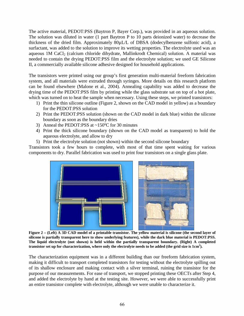
The active material, PEDOT:PSS (Baytron P, Bayer Corp.), was provided in an aqueous solution. The solution was diluted in water (1 part Baytron P to 10 parts deionized water) to decrease the thickness of the dried film. Approximately 80µL/L of DBSA (dodecylbenzene sulfonic acid), a surfactant, was added to the solution to improve its wetting properties. The electrolyte used was an aqueous 1M CaCl2 (calcium chloride dihydrate, Mallinkrodt Chemical) solution. A material was needed to contain the drying PEDOT:PSS film and the electrolyte solution; we used GE Silicone II, a commercially available silicone adhesive designed for household applications. The transistors were printed using our group’s first generation multi-material freeform fabrication system, and all materials were extruded through syringes. More details on this research platform can be found elsewhere (Malone et al., 2004). Annealing capability was added to decrease the drying time of the PEDOT:PSS film by printing while the glass substrate sat on top of a hot plate, which was turned on to heat the sample when necessary. Using these steps, we printed transistors:
1) Print the thin silicone outline (Figure 2, shown on the CAD model in yellow) as a boundary for the PEDOT:PSS solution
2) Print the PEDOT:PSS solution (shown on the CAD model in dark blue) within the silicone boundary as soon as the boundary dries
3) Anneal the PEDOT:PSS at ~150ºC for 30 minutes 4) Print the thick silicone boundary (shown on the CAD model as transparent) to hold the
aqueous electrolyte, and allow to dry 5) Print the electrolyte solution (not shown) within the second silicone boundary
Transistors took a few hours to complete, with most of that time spent waiting for various components to dry. Parallel fabrication was used to print four transistors on a single glass plate.
Figure 2 – (Left) A 3D CAD model of a printable transistor. The yellow material is silicone (the second layer of silicone is partially transparent here to show underlying features), while the dark blue material is PEDOT:PSS. The liquid electrolyte (not shown) is held within the partially transparent boundary. (Right) A completed transistor set up for characterization, where only the electrolyte needs to be added (the grid size is 1cm2). The characterization equipment was in a different building than our freeform fabrication system, making it difficult to transport completed transistors for testing without the electrolyte spilling out of its shallow enclosure and making contact with a silver terminal, ruining the transistor for the purpose of our measurements. For ease of transport, we stopped printing these OECTs after Step 4, and added the electrolyte by hand at the testing site. However, we were able to successfully print an entire transistor complete with electrolyte, although we were unable to characterize it.
66
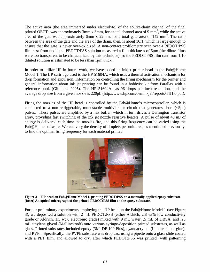
The active area (the area immersed under electrolyte) of the source-drain channel of the final printed OECTs was approximately 3mm x 3mm, for a total channel area of 9 mm2, while the active area of the gate was approximately 6mm x 22mm, for a total gate area of 142 mm2. The ratio between the area of the gate and the area of the drain, then, is about 16:1, which is large enough to ensure that the gate is never over-oxidized. A non-contact profilometry scan over a PEDOT:PSS film cast from undiluted PEDOT:PSS solution measured a film thickness of 5µm (the dilute films were too transparent to be characterized by this technique), so the PEDOT:PSS film cast from 1:10 diluted solution is estimated to be less than 1µm thick. In order to utilize IJP in future work, we have added an inkjet printer head to the Fab@Home Model 1. The IJP cartridge used is the HP 51604A, which uses a thermal activation mechanism for drop formation and expulsion. Information on controlling the firing mechanism for the printer and general information about ink jet printing can be found in a hobbyist kit from Parallax with a reference book (Gilliland, 2005). The HP 51604A has 96 drops per inch resolution, and the average drop size from a given nozzle is 220pL (http://www.hp.com/oeminkjet/reports/TIJ1.0.pdf). Firing the nozzles of the IJP head is controlled by the Fab@Home’s microcontroller, which is connected to a non-retriggerable, monostable multivibrator circuit that generates short (~5µs) pulses. These pulses are amplified by a hex buffer, which in turn drives a Darlington transistor array, providing fast switching of the ink jet nozzle resistive heaters. A pulse of about 40 mJ of energy is delivered each time the nozzles fire, and this firing frequency can be varied using the Fab@Home software. We can vary the density of droplets per unit area, as mentioned previously, to find the optimal firing frequency for each material printed.
Figure 3 – IJP head on Fab@Home Model 1, printing PEDOT:PSS on a manually-applied epoxy substrate. (Inset) An optical micrograph of the printed PEDOT:PSS film on the epoxy substrate. For our preliminary experiments employing the IJP head on the Fab@Home Model 1 (see Figure 3), we deposited a solution with 2 mL PEDOT:PSS (either Aldrich, 2.8 wt% low conductivity grade or Aldrich, 1.3 wt% electronic grade) mixed with 9 mL water, .5 mL of DBSA, and .25 mL ethylene glycol (Mallinckrodt) onto various syringe-deposition printed substrates, as well as glass. Printed substrates included epoxy (3M, DP 100 Plus), cyanoacrylate (Loctite, super glue), and PVPh. Specifically, the PVPh substrate was drop cast using a pipette onto a glass slide coated with a PET film, and allowed to dry, after which PEDOT:PSS was printed (with patterning
1 mm
67
performed by hand) on top of the PVPh. PEDOT:PSS films ranged in size between 1 and 2 in2, with a thickness of approximately 1µm.
Testing The syringe deposition-printed transistors needed additional modifications to connect to the characterization equipment. These modifications will be part of another printed component (like a wire) when the transistors are connected to a larger printed circuit. Conducting colloidal silver ink (Stan Rubenstein Assoc.) thinned 5:2 with toluene was painted onto the gate, source, and drain contacts (see Figure 2) and allowed to dry. Care was taken so that the silver remained far from the electrolyte solution. The silver ink provided a large contact area between the transistor and external probes, which were used to connect the transistor to the electrical measurement setup. The electrolyte was added to the transistors with an eyedropper at the testing site. It was allowed to sit for several minutes, giving its calcium ions a chance to cross-link the PEDOT:PSS film, before the transistors were tested. Transistors were characterized using two Keithley 2400 Source-Measure units interfaced with a LabVIEW VI. The source terminal of each OECT was grounded while voltages were applied to the gate and drain terminals. The response of each transistor was determined by measuring the current flowing between the gate and source, referred to as the “gate current,” and between the drain and source, called the “drain current.” Resistivity data of PEDOT:PSS films were measured with a four-point probe, using a DC power supply and a multimeter to measure the voltage drop across a fixed distance of PEDOT:PSS film.
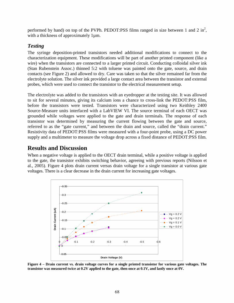
Results and Discussion When a negative voltage is applied to the OECT drain terminal, while a positive voltage is applied to the gate, the transistor exhibits switching behavior, agreeing with previous reports (Nilsson et al., 2005). Figure 4 plots drain current versus drain voltage for a single transistor at various gate voltages. There is a clear decrease in the drain current for increasing gate voltages.
-0.35
-0.3
-0.25
-0.2
-0.15
-0.1
-0.05
0
0.05
-0.6-0.5-0.4-0.3-0.2-0.10
Drain Voltage (V)
Dra
in C
urr
ent
(uA
)
Vg = 0.2 V
Vg = 0.2 V
Vg = 0.1 V
Vg = 0.0 V
Figure 4 – Drain current vs. drain voltage curves for a single printed transistor for various gate voltages. The transistor was measured twice at 0.2V applied to the gate, then once at 0.1V, and lastly once at 0V.
68
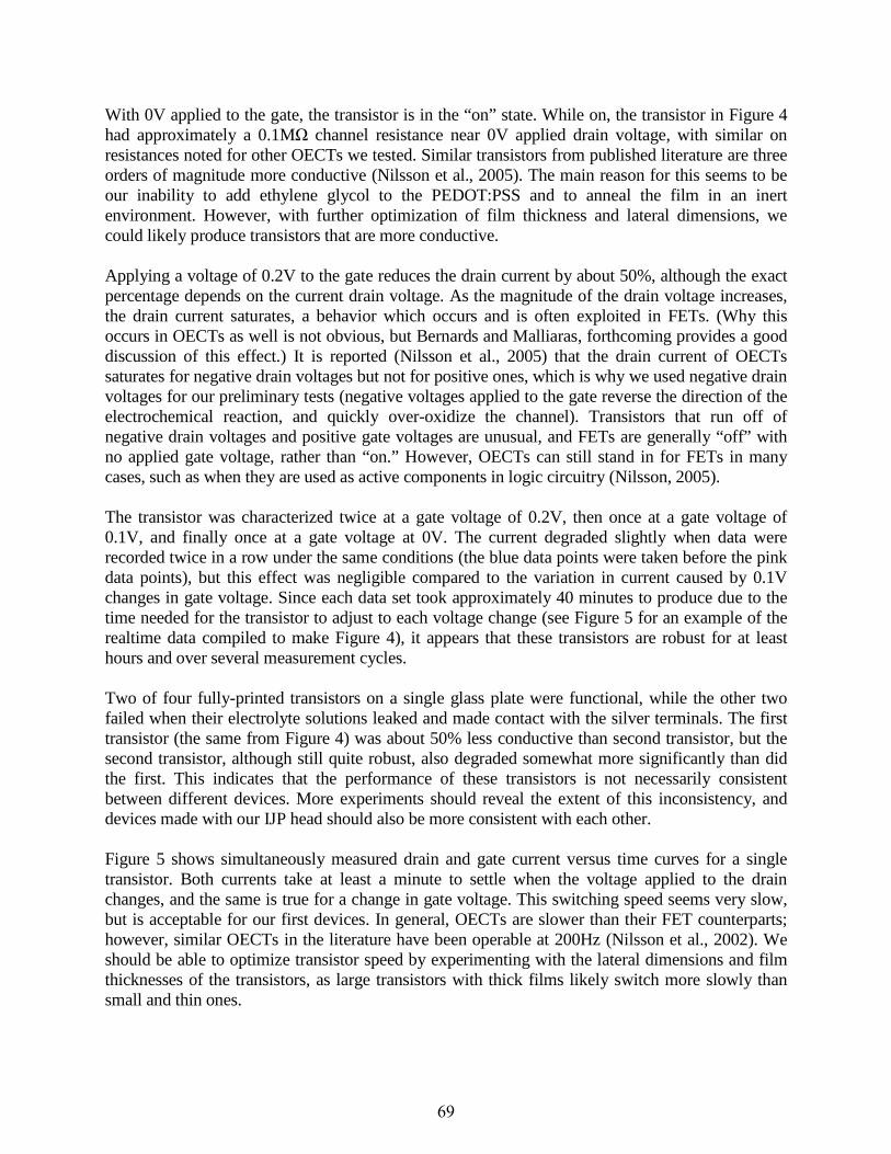
With 0V applied to the gate, the transistor is in the “on” state. While on, the transistor in Figure 4 had approximately a 0.1MΩ channel resistance near 0V applied drain voltage, with similar on resistances noted for other OECTs we tested. Similar transistors from published literature are three orders of magnitude more conductive (Nilsson et al., 2005). The main reason for this seems to be our inability to add ethylene glycol to the PEDOT:PSS and to anneal the film in an inert environment. However, with further optimization of film thickness and lateral dimensions, we could likely produce transistors that are more conductive. Applying a voltage of 0.2V to the gate reduces the drain current by about 50%, although the exact percentage depends on the current drain voltage. As the magnitude of the drain voltage increases, the drain current saturates, a behavior which occurs and is often exploited in FETs. (Why this occurs in OECTs as well is not obvious, but Bernards and Malliaras, forthcoming provides a good discussion of this effect.) It is reported (Nilsson et al., 2005) that the drain current of OECTs saturates for negative drain voltages but not for positive ones, which is why we used negative drain voltages for our preliminary tests (negative voltages applied to the gate reverse the direction of the electrochemical reaction, and quickly over-oxidize the channel). Transistors that run off of negative drain voltages and positive gate voltages are unusual, and FETs are generally “off” with no applied gate voltage, rather than “on.” However, OECTs can still stand in for FETs in many cases, such as when they are used as active components in logic circuitry (Nilsson, 2005). The transistor was characterized twice at a gate voltage of 0.2V, then once at a gate voltage of 0.1V, and finally once at a gate voltage at 0V. The current degraded slightly when data were recorded twice in a row under the same conditions (the blue data points were taken before the pink data points), but this effect was negligible compared to the variation in current caused by 0.1V changes in gate voltage. Since each data set took approximately 40 minutes to produce due to the time needed for the transistor to adjust to each voltage change (see Figure 5 for an example of the realtime data compiled to make Figure 4), it appears that these transistors are robust for at least hours and over several measurement cycles. Two of four fully-printed transistors on a single glass plate were functional, while the other two failed when their electrolyte solutions leaked and made contact with the silver terminals. The first transistor (the same from Figure 4) was about 50% less conductive than second transistor, but the second transistor, although still quite robust, also degraded somewhat more significantly than did the first. This indicates that the performance of these transistors is not necessarily consistent between different devices. More experiments should reveal the extent of this inconsistency, and devices made with our IJP head should also be more consistent with each other. Figure 5 shows simultaneously measured drain and gate current versus time curves for a single transistor. Both currents take at least a minute to settle when the voltage applied to the drain changes, and the same is true for a change in gate voltage. This switching speed seems very slow, but is acceptable for our first devices. In general, OECTs are slower than their FET counterparts; however, similar OECTs in the literature have been operable at 200Hz (Nilsson et al., 2002). We should be able to optimize transistor speed by experimenting with the lateral dimensions and film thicknesses of the transistors, as large transistors with thick films likely switch more slowly than small and thin ones.
69
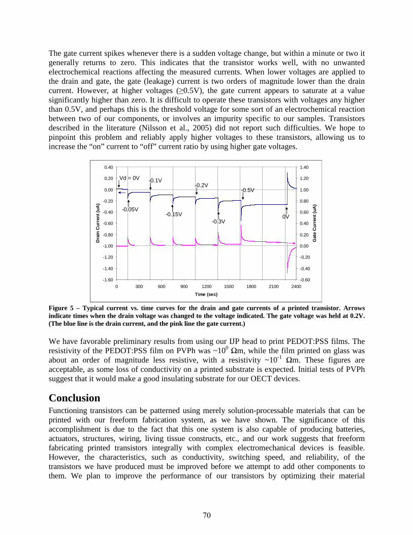
The gate current spikes whenever there is a sudden voltage change, but within a minute or two it generally returns to zero. This indicates that the transistor works well, with no unwanted electrochemical reactions affecting the measured currents. When lower voltages are applied to the drain and gate, the gate (leakage) current is two orders of magnitude lower than the drain current. However, at higher voltages (≥0.5V), the gate current appears to saturate at a value significantly higher than zero. It is difficult to operate these transistors with voltages any higher than 0.5V, and perhaps this is the threshold voltage for some sort of an electrochemical reaction between two of our components, or involves an impurity specific to our samples. Transistors described in the literature (Nilsson et al., 2005) did not report such difficulties. We hope to pinpoint this problem and reliably apply higher voltages to these transistors, allowing us to increase the “on” current to “off” current ratio by using higher gate voltages.
-1.60
-1.40
-1.20
-1.00
-0.80
-0.60
-0.40
-0.20
0.00
0.20
0.40
0 300 600 900 1200 1500 1800 2100 2400
Time (sec)
Dra
in C
urr
ent (
uA
)
-0.60
-0.40
-0.20
0.00
0.20
0.40
0.60
0.80
1.00
1.20
1.40
Gat
e C
urr
ent (
uA)
Vd = 0V
-0.05V
-0.1V
-0.15V
-0.2V
-0.3V
-0.5V
0V
-1.60
-1.40
-1.20
-1.00
-0.80
-0.60
-0.40
-0.20
0.00
0.20
0.40
0 300 600 900 1200 1500 1800 2100 2400
Time (sec)
Dra
in C
urr
ent (
uA
)
-0.60
-0.40
-0.20
0.00
0.20
0.40
0.60
0.80
1.00
1.20
1.40
Gat
e C
urr
ent (
uA)
Vd = 0V
-0.05V
-0.1V
-0.15V
-0.2V
-0.3V
-0.5V
0V
-1.60
-1.40
-1.20
-1.00
-0.80
-0.60
-0.40
-0.20
0.00
0.20
0.40
0 300 600 900 1200 1500 1800 2100 2400
Time (sec)
Dra
in C
urr
ent (
uA
)
-0.60
-0.40
-0.20
0.00
0.20
0.40
0.60
0.80
1.00
1.20
1.40
Gat
e C
urr
ent (
uA)
Vd = 0V
-0.05V
-0.1V
-0.15V
-0.2V
-0.3V
-0.5V
0V
Figure 5 – Typical current vs. time curves for the drain and gate currents of a printed transistor. Arrows indicate times when the drain voltage was changed to the voltage indicated. The gate voltage was held at 0.2V. (The blue line is the drain current, and the pink line the gate current.) We have favorable preliminary results from using our IJP head to print PEDOT:PSS films. The resistivity of the PEDOT:PSS film on PVPh was ~100 Ωm, while the film printed on glass was about an order of magnitude less resistive, with a resistivity ~10-1 Ωm. These figures are acceptable, as some loss of conductivity on a printed substrate is expected. Initial tests of PVPh suggest that it would make a good insulating substrate for our OECT devices.
Conclusion Functioning transistors can be patterned using merely solution-processable materials that can be printed with our freeform fabrication system, as we have shown. The significance of this accomplishment is due to the fact that this one system is also capable of producing batteries, actuators, structures, wiring, living tissue constructs, etc., and our work suggests that freeform fabricating printed transistors integrally with complex electromechanical devices is feasible. However, the characteristics, such as conductivity, switching speed, and reliability, of the transistors we have produced must be improved before we attempt to add other components to them. We plan to improve the performance of our transistors by optimizing their material
70
properties, lateral dimensions, and film thicknesses. Our ink jet printer (IJP) head will give us more flexibility in patterning devices more reliably and at smaller scales than was possible with syringes, and may allow us to experiment with printing other types of transistors, like OFETs, in the future. Our current aqueous electrolyte may be easy to handle, but it has many disadvantages. The low-viscosity solution can spill out of its enclosure or evaporate, unnecessarily lowering transistor yield and durability. Since PEDOT:PSS in solution is aqueous, damage to the PEDOT:PSS film is also a possibility when using an aqueous electrolyte. The dried film is not easily water-soluble, but a slight loss in conductivity occurred over about an hour of the PEDOT:PSS being immersed in electrolyte solution, and it is unlikely that our current transistors would have a particularly long shelf life (even ignoring electrolyte evaporation). It will be important to develop an electrolyte that has a high conductivity, is compatible with all our other materials, and does not evaporate. Ultimately, we wish to print working transistors on printable substrates. We are beginning to characterize how the properties of PEDOT:PSS are affected by a printable substrate, but will soon be ready to begin printing transistors on these substrates with the additional aid of our IJP head. These ongoing improvements to our freeform fabrication system and to the performance of the transistors it prints, and work towards making printed transistors ready to integrate into larger printed systems, will greatly facilitate our efforts to create fully-functional electromechanical printed devices with a single machine.
Acknowledgments This work was supported in part by the Cornell Center for Materials Research – Research Experience for Undergraduates program, which is supported by the National Science Foundation. R. H. acknowledges Sujit S. Datta for fruitful discussions.
References Andersson, P., D. Nilsson, P. Svensson, M. Chen, A. Malmström, T. Remonen, T. Kugler, and M.
Berggren. 2002. Active matrix displays based on all-organic electrochemical smart pixels printed on paper. Adv. Mater. 14:1460-64.
Berggren, M., D. Nilsson, and N. D. Robinson. 2007. Organic materials for printed electronics. Nature Materials 6:3-5.
Bernards, D. A., and G. G. Malliaras. Steady-state and transient behavior of organic electrochemical transistors. Advanced Functional Materials (forthcoming).
Bernards, D. A., G. G. Malliaras, G. E. S. Toombes, and S. M. Gruner. 2006. Gating of an organic transistor through a bilayer membrane with ion channels. Appl. Phys. Lett. 89:053505.
Chen, B., T. H. Cui, Y. Liu, and K. Varahramyan. 2003. All-polymer RC filter circuits fabricated with inkjet printing technology. Solid-State Electronics 47:841-47.
Chen, M. 2005. Printed electrochemical devices using conducting polymers as active materials on flexible substrates. Proceedings of the IEEE 93:1339-47.
Chen, M. 2006. Threshold-voltage tuning characteristics of all-organic electrochemical vertical rectifiers on flexible substrates. IEEE Electron Device Letters 27:243-245.
Clemens, W., W. Fix, J. Ficker, A. Knobloch, and A. Ullmann. 2004. From polymer transistors toward printed electronics. Journal of Materials Research 19:1963-73.
71
Cohen, D. L., E. Malone, H. Lipson, and L. Bonassar. 2006. 3D direct printing of heterogeneous tissue implants. Tissue Engineering 12:1325-35.
Dimitrakopoulos, C., and D. Mascaro. 2001. Organic thin-film transistors: A review of recent advances. IBM Journal of Research and Development 45:11-27.
Ghosh, S., J. Rasmusson, and O. Inganäs. 1998. Supramolecular self-assembly for enhanced conductivity in conjugated polymer blends: Ionic crosslinking in blends of poly(3,4-ethylenedioxythiopene)-poly(styrenesulfonate) and poly(vinylpyrrolidone). Adv. Mater. 10:1097-99.
Gilliland, M. 2005. Inkjet Applications, Circuits with BASIC Stamp 2 and SX microcontrollers. N.p.: Woodglen Press.
Groenendaal, L. B., F. Jonas, D. Freitag, H. Pielartzik, and J. R. Reynolds. 2000. Poly(3,4-ethylenedioxythiopene) and its derivatives: past, present, and future. Adv. Mater. 12:481-94.
Hedges, M., M. Renn, and M. Kardos. Mesoscale deposition technology for electronics applications. 5th International Conference on Polymers and Adhesives in Microelectronics and Photonics, 2005, 53-7
Horowitz, G. 1998. Organic field-effect transistors. Adv. Mater. 10:365-377. Katz, H. E. 2004. Recent advances in semiconductor performance and printing processed for
organic transistor-based electronics. Chem. Mater. 16:4748-56 Kim, W. H., G. P. Kushto, H. Kim, and Z. H. Kafafi. 2003. Effect of annealing on the electrical
properties and morphology of a conducting polymer used as an anode in organic light-emitting devices. Journal of Polymer Science: Part B: Polymer Physics 41:2522-8.
Lu, J., N. J. Pinto, and A. G. MacDiarmid. 2002. Apparent dependence of conductivity of a conducting polymer on an electric field in a field-effect transistor configuration. J. Appl. Phys. 92:6033-38.
MacDiarmid, A. 2002. Synthetic metals: A novel role for organic polymers. Synthetic Metals 125:11-22.
Mabeck, J. T. and G. G. Malliaras. 2006. Chemical and biological sensors based on organic thin-film transistors. Anal. Bioanal. Chem. 384:343-53.
Malone, E., M. Berry, and H. Lipson. Freeform fabrication of zinc-air batteries with tailored geometry and performance. Rapid Prototyping Journal (submitted).
Malone, E. and H. Lipson. 2006. Freeform fabrication of ionomeric polymer-metal composite actuators. Rapid Prototyping Journal 12:244-53.
Malone, E. and H. Lipson. 2007. Fab@Home: The personal desktop fabricator kit. Rapid Prototyping Journal (forthcoming).
Malone, E., K. Rasa, D. L. Cohen, T. Isaacson, H. Lashley, and H. Lipson. 2004. Freeform fabrication of 3D zinc-air batteries and functional electro-mechanical assemblies. Rapid Prototyping Journal 10:58-69.
Nilsson, D., M. Chen, T. Kugler, T. Remonen, M. Armgarth, and M. Berggren. 2002. Bi-stable and dynamic current modulation in electrochemical organic transistors. Adv. Mater. 14:51-4.
Nilsson, D., N. Robinson, M. Berggren, and R. Forchheimer. 2005. Electrochemical logic circuits. Adv. Mater. 17:353-8.
Ouyang, J., X. Qianfei, C. Chi-Wei, Y. Yang, G. Li, and J. Shinar. 2004. On the mechanism of conductivity enhancement in poly(3,4-ethylenedioxythiopene):poly(styrene sulfonate) film through solvent treatment. Polymer 45:8443-50.
72
Paul, K. E., W. S. Wong, S. E. Ready, and R. A. Street. 2003. Additive jet printing of polymer thin-film transistors. Appl. Phys. Lett. 83:2070-2.
Robinson, N. D., P. Svensson, D. Nilsson, and M. Berggren. 2006. On the current saturation observed in electrochemical polymer transistors. Journal of the Electrochemical Society 153:H39-44.
Sandberg, H. G. O., T. G. Bäcklund, R. Österbacka, and H. Stubb. 2004. High-performance all-polymer transistors utilizing a hygroscopic insulator. Adv. Mater. 16:1112-5.
White, H. S., G. P. Kittlesen, and M. S. Wrighton. 1984. Chemical derivatization of an array of three gold microelectrodes with polypyrrole: fabrication of a molecule-based transistor. J. Am. Chem. Soc.106:5375-77.
Ziemelis, K. 1998. Putting it on plastic. Nature 393:619-20.
73