Embed Size (px)
Citation preview

Chris Rowen
CTO - IP Group
August 2014
Flexible Architectures for Scalable Flash Controllers

2 © 2014 Cadence Design Systems, Inc. All rights reserved.
1. Energy per operation scales with distance: primitive op to cloud access
2. >1010 energy range drives system architecture: Move computation closer to data
3. Emergence of Dataplane Processor Units (DPUs)
4. Cloud data aggregation [disk farm] vs personal data aggregation [SSD]
5. Flash has unique role in capacity vs. energy
6. Flash potential not yet exploited
• Bandwidth
• Transaction rate
Why? Need faster “smarts”
Where’s My Data?
Cloud access
Disk access
DRAM access
L3 cache (1MB)
L2 cache (32KB)
L1 cache (8KB)
Regfile Operation
1E-12
1E-11
1E-10
1E-09
1E-08
1E-07
1E-06
1E-05
1E-04
1E-03
1E-02 1E+00 1E+02 1E+04 1E+06 1E+08
Ap
pro
xim
ate
En
erg
y p
er
64
b o
p (
J)
Range (mm)
1000km
16nm

3 © 2014 Cadence Design Systems, Inc. All rights reserved.
• CPU : Central Processing Unit
• GPU : Graphics Processing Unit
• NPU : Network Processing Unit
• Various DSPs – APU : Audio Processing Unit
– VPU : Vision Processing Unit
– WPU : Wireless Processing Units
Processing My Data! Proliferation of Dataplane Processor Units (DPUs)
Dataplane Processor
Units (DPUs)
SPU : Storage Processing Unit

4 © 2014 Cadence Design Systems, Inc. All rights reserved.
Storage Processors
•Tensilica dataplane processors
•Fully C programmable
•Optimized instruction set and interface capability
•Widely used architecture in storage systems
Controllers
•Async
•ONFI 1, 2, 3, 4 Toggle 1, 2, 3
•BCH ECC
•Advanced Features
PHYs
•ONFi 1, 2, 3, 4 and Toggle 1, 2, 3
•Soft Deliverable
•Supports all Fabs and technologies
•Scalable from 1 to >20 lanes
Software
•Core Firmware Driver
•Reference Linux Driver
•Virtual Reference Platform
Integrated Solutions
•Controller and PHY integrated and verified
What are the Ingredients for Storage Success? Solutions to fit customer needs
Photo courtesy of PC World

5 © 2014 Cadence Design Systems, Inc. All rights reserved.
Storage Processors Unify Subsystem Design Complements Cadence Storage Interface IP
MEMORY
PHY
DDR
ONFi Toggle
PCIe for NVMe
FLASH
CTL
PH
Y
CT
L
HOST
PH
Y
CT
L
Processor(s)
Other I/O
Flash
Memory Host
Xtensa-based Storage
Processors Plus USB, eMMC
and SDIO solutions

6 © 2014 Cadence Design Systems, Inc. All rights reserved.
Key Questions • How can we scale interface performance?
• How does processor handle complex protocols?
• How do you improve both time-to-market and differentiation?
Issues in Storage System Design
Needs
Flexibility to support complex, evolving storage algorithms
Scalability in capacity, bandwidth and transaction rate
Robustness and data integrity
Silicon cost
Time to market for differentiated platform

7 © 2014 Cadence Design Systems, Inc. All rights reserved.
Cadence Storage IP
MEMORY
PHY
DDR • Highest performance
• Lowest Power memory systems
• Robust operation (fine grain delay)
• Smaller, high yield
ONFi, Toggle • ONFi 2.3, 3.0 : Toggle 1,2
• 95% max theoretical ONFI3
thruput
• All addressing schemes
• Fastest ECC
• Robust - no failures
• Supports all major NAND
devices/suppliers
PCIe • Controller:
• Highest throughput, lower latency,
pre-verified
• Phy: • Lowest power, high performance,
robust, easy integration
Storage Controller
FLASH
CTL
PH
Y
CT
L
HOST
PH
Y
CT
L
Processor(s)
Other I/O
Flash
Memory Host
USB
Xtensa • Most energy efficient
• Virtually unlimited I/O
• Easy development &
maintenance in C with GUI

8 © 2014 Cadence Design Systems, Inc. All rights reserved.
Other I/O
Flash Systems with Smart Storage Processors Example System
NAND
Flash
CTRL 1
Boot
ROM I/F
NAND
Flash
CTRL 2
AXI Interconnect Fabric
CE(7:0) D(7:0)
CE(7:0) D(7:0)
AXI-APB APB Interconnect Bus
UART GPIO Timers I2C
PCIe PHY
Host
Interface
PCIe Controller
PCIe 4 @ x 4 lanes
Flash PHY Flash PHY DDR PHY
DDR SDRAM
SPI
NOR FLASH
Storage Processor
1
DDR Controller
DRAM
3,200MT/s * 64 b=
25.6GB/s peak
16Gbps * 4 lanes =
8GB/s peak
NVMe Processor
Software-managed SRAM block buffer (~256KB)
AES Encrypt
LZ77 Compress
Mux
NAND
Flash
CTRL 15
NAND
Flash
CTRL 16
CE(7:0) D(7:0)
CE(7:0) D(7:0)
Flash PHY Flash PHY
Storage Processor
8
AES Encrypt
LZ77 Compress
Mux
. . .
400MB/s per channel x 16 channels = 6.4GB/s peak
NAND FLASH NAND FLASH NAND FLASH NAND FLASH
Capacity
4-32 TB
Flash
NVMe Processor
0
NAND FLASH NAND FLASH NAND FLASH NAND FLASH

9 © 2014 Cadence Design Systems, Inc. All rights reserved.
Parameter Value
16 OnFi 3 channels @ 400MB/s 6.4GB per second
4KB logical block size Up to 1.6M logical block requests/sec
Up to 4 devices per OnFi channel @ 4Tb per device 32TB capacity
Total logical blocks to map in system 8B blocks
Flash block organization 64 pages of ~2KB = 128K flash block
Processor clock 1000MHz
Flash page service time 2KB at 800MB/s =
~400 cycles/block
Example System Parameters

10 © 2014 Cadence Design Systems, Inc. All rights reserved.
Cadence Complete Ingredients: ONFi NAND Flash Controller + PHY
• Supports all major NAND devices & interfaces
• Fully integrated controller and PHY
• Integrated or system-side Data DMA
• FlexBCH: Full optimized hardware with
flexible correction strength and codeword size
selection
• Comand Processing:
o Interleaving and queuing with context
saving
o Repeating commands through Super
Sequence
o Support for undocumented instructions
• Boot from flash preconfigured with pin
strapping
• Hardware-assisted Bad Block Managment
• Full Software Deliverables:
• Driver
• Wrapper
• Diags
• Demo
High performance architecture
enables 95% of maximum
theoretical performance of
ONFi3 interface

11 © 2014 Cadence Design Systems, Inc. All rights reserved.
PCIe 1,2,3,4 Controller: o Best in class performance, >95% Link utilization
o Scalable design: 1 to 16 lanes
o Proven Virtualization and Bifurcation capabilities
• Efficient and Proven o Energy efficient designs with low-power ECNs (L1
substates, OBFF, LTR, ASPM Optionality)
o In Silicon with multiple PHYs, customers certified
• PCI Specifications: PCI Express v1.1, 2.1, 3.0,
and 4.0 (Beta), Intel PIPE v3.0 and 4.x, SRIOV v1.1
Cadence Complete Ingredients
Cadence PCI Express® Controller IP + PHY
PCIe Gen 4-ready PHY with
FinFET Realization
• Less power, less jitter, better data
recovery o Power saving with leakage optimizations
o Combined LC-VCO and RO PLLs
o Supports >30 dB channel loss
• Compliant Standards o PCIe v1.1, 2.1,3, and 4; Intel PIPE 4.0
o 10G-KR, XAUI, QSGMII/SGMII
• Key Features
o 5 Tap DFE with adaptive CTLE and
offset correction
o Auto-calibration of on-chip termination
o x1- x16 configurations
o Scalable PIPE width w/ standard
AMBA-APB interface
• IP Readiness: Test chip T/O done
• IP Products: o Root Ports, End Points,
Dual mode
• Integrated Solution o PCIe Controller
o Proven PHYs
o Software: Core
Driver/Linux Reference
Driver
12 © 2014 Cadence Design Systems, Inc. All rights reserved.
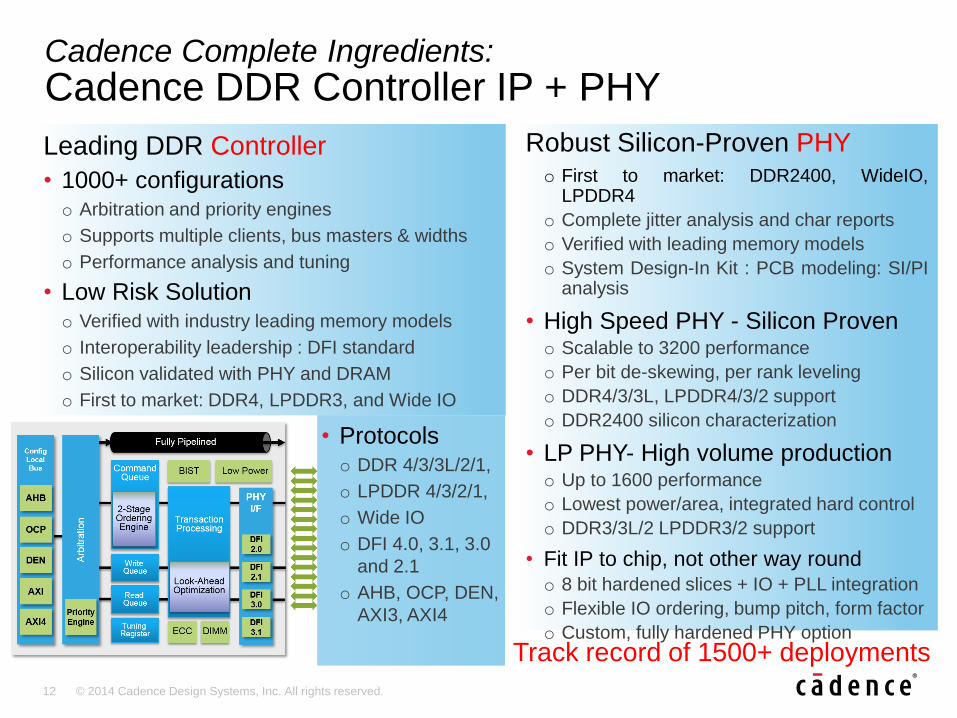
Leading DDR Controller
• 1000+ configurations o Arbitration and priority engines
o Supports multiple clients, bus masters & widths
o Performance analysis and tuning
• Low Risk Solution o Verified with industry leading memory models
o Interoperability leadership : DFI standard
o Silicon validated with PHY and DRAM
o First to market: DDR4, LPDDR3, and Wide IO
Cadence Complete Ingredients:
Cadence DDR Controller IP + PHY
Track record of 1500+ deployments
Robust Silicon-Proven PHY o First to market: DDR2400, WideIO,
LPDDR4
o Complete jitter analysis and char reports
o Verified with leading memory models
o System Design-In Kit : PCB modeling: SI/PI analysis
• High Speed PHY - Silicon Proven o Scalable to 3200 performance
o Per bit de-skewing, per rank leveling
o DDR4/3/3L, LPDDR4/3/2 support
o DDR2400 silicon characterization
• LP PHY- High volume production o Up to 1600 performance
o Lowest power/area, integrated hard control
o DDR3/3L/2 LPDDR3/2 support
• Fit IP to chip, not other way round o 8 bit hardened slices + IO + PLL integration
o Flexible IO ordering, bump pitch, form factor
o Custom, fully hardened PHY option
• Protocols o DDR 4/3/3L/2/1,
o LPDDR 4/3/2/1,
o Wide IO
o DFI 4.0, 3.1, 3.0
and 2.1
o AHB, OCP, DEN,
AXI3, AXI4

13 © 2014 Cadence Design Systems, Inc. All rights reserved.
Cadence ingredient that binds it all together: Tensilica automated hardware/software synthesis
Processor
Extensions
Xtensa Processor Generator
Full hardware design Source pre-verified RTL, EDA scripts, test suite
Customized software tools C/C++ compiler Debuggers,
Simulators, RTOSes
1. Select from menu
2. Explicit instruction
description (TIE)
Processor configuration
Architects’ needs:
• Faster command queue
processing
• More memory bandwidth
• Hide latency to DDR
• Rapid search of huge
mapping tables
• Continuous software
upgrade of EVERYTHING
No manual intervention needed in
hardware or software completeness

14 © 2014 Cadence Design Systems, Inc. All rights reserved.
Increasing Computational Throughput In Xtensa Processors – more choices
Add new instructions • Raise overall performance
• Accelerate critical functions
• Often over 10x performance improvement
Improve register availability • Add more registers for the compiler to use
• Set custom widths, up to 1024bits, to keep area as low as possible
Execute multiple instructions at once • Arbitrary new VLIW instruction bundles
• Automatically used by compiler
• A general purpose performance improvement
Increase local memory bandwidth • Multiple Load/Store units
• Up to 1024bits total per cycle
DMA and direct-connect to system memories and logic • Overcome bandwidth/latency bus bottlenecks
• For Command Queues/Code overlays etc.
• No processor cycles required to move data

15 © 2014 Cadence Design Systems, Inc. All rights reserved.
• For each logical block in file systems, find flash block
• Update usage statistics as accessed
• Large-scale hash tables for speed and scalability
• Instruction Set: Fast Hash, Table search with >232 entries
Mapping
• Cache or temporarily write data in available unwritten pages
• Migrate data to reduce fragmentation
• Reclaim deleted data
• Instruction Set: Fast data movement
Write management
• Track lifetime writes per flash block and write less-used, blocks
• Track read-disturb – accumulate reads since last write
• Rewrite [move] data to refresh data
• Instruction Set: Parse and update data-structures
Wear leveling
• Requests: For each logical read/write, determine and schedule sequence of reads and writes required
• Response: On completion, reply to host with data/status
• Instruction Set: Command parsing/dispatch, direct queue I/O
Command processing
Tasks for Flash Management Processing

16 © 2014 Cadence Design Systems, Inc. All rights reserved.
• Built on widely popular Xtensa processor family
• Implemented in Tensilica Instruction Extension (TIE) code
• Add: – 64b register file
– 64b non-blocking read/write queue
– 64b x N entry local tag cache
– Parity protection on added register files and queues
– 3-way instruction issue in 64b VLIW instruction width
• Operations – 64b load/store including address update load/store
– “parsing” load and “packing” store operates on up to 3 32b, 16b, 8b fields
– chaining loads checks tag match and null pointers
– Non-blocking read and write requests to memory: 64b address, hashing
– Tag cache management operations: lookup, find_victim, check_dirty
– Multiple issue slots for bit field insertion and extraction
Example: Instruction Set for Storage

17 © 2014 Cadence Design Systems, Inc. All rights reserved.
Generalized List Processing Instruction Set Gives Significant Performance Boost
0
1
2
3
4
5
insert/updatelinked list
lookup linked list remove linkedlist
memcopy GeoMean
Cyc
le P
erf
orm
an
ce
(Te
ns
ilic
a 2
12
GP
RIS
C =
1.0
)

18 © 2014 Cadence Design Systems, Inc. All rights reserved.
• All the key building blocks for high-performance intelligent storage
• Cadence has the state-of-the-art design ingredients: controllers and PHYs
o ONFi
o DDR
o PCIe
• New category of DPUs - Storage Processor Unit raises performance by an order-of-magnitude
• Performance AND generality unleashes system architect creativity
• 40 leading companies already using Cadence flash-specific IP in major SOC platforms
Wrap-up