Embed Size (px)
Citation preview

n
Georgiev, V. P., Amoroso, S. M., Vila-Nadal, L., Busche, C., Cronin, L., and Asenov, A. (2014) FDSOI Molecular Flash Cell with Reduced Variability for Low Power Flash Applications. In: 44th European Solid-State Device Research Conference (ESSDERC), Venice, Italy, 22-26 Sep 2014, pp. 353-356. ISBN 9781479943760. There may be differences between this version and the published version. You are advised to consult the publisher’s version if you wish to cite from it.
http://eprints.gla.ac.uk/104304/
Deposited on: 16 February 2016
Enlighten – Research publications by members of the University of Glasgow http://eprints.gla.ac.uk
FDSOI molecular flash cell with reduced variability for low power flash applications
Vihar P. Georgiev1, Salvatore M. Amoroso1, Laia Vilà-Nadal2, Cristoph Busche2, Leroy Cronin2 and Asen Asenov1§
1Device Modelling Group, School of Engineering, University of Glasgow, G12 8LT Glasgow, UK § Gold Standard Simulations Ltd., G12 8LT Glasgow, UK
2WestCHEM, School of Chemistry, University of Glasgow, G12 8QQ Glasgow, UK e-mail: [email protected]
Abstract—In this work we present a modeling study of a conceptual low power non-volatile memory cell based on inorganic molecular metal oxide clusters (polyoxometalates (POM)) as a storage media embedded in the gate dielectric of a Fully Depleted SOI (FD SOI) with reduced statistical variability. The simulations were carried out using a multi-physics simulation framework, which allows us to evaluate the variability in the programming window of the molecular based flash cell with an 18 nm gate length. We have focused our study on the threshold voltage variability influenced by random dopant fluctuations and random special fluctuations of the molecules in the floating gate of the flash-cell. Our simulation framework and conclusions can be applied not only to POM-based flash cell but also to flash cells based on alternative molecules used as a storage media.
I. INTRODUCTION The use of inorganic molecules known as
polyoxometalates (POMs) (see Fig. 1) to form the storage media in flash memory cells (see Fig. 2) could offer several very important advantages over the conventional polysilicon floating gate (FG) flash cells [1], [2]. It is believed that the POMS are more compatible with existing CMOS processes than organic molecules as by their nature they consist of oxygen atoms similar to SiO2. The interest in POMs for flash cell applications stems from the fact that POMs are highly redox active molecules and that they also can be doped with electronically active heteroatoms [3]. Moreover, they can undergo multiple times reversible reduction/oxidation, which makes them attractive candidates for multi-bit storage in flash memory cells. The molecular charge storage is very localised, thus minimising cross-cell capacitive coupling (arising from charge redistribution on the sides of a poly-Si FG and being one of the most critical issues with flash memories). Although this benefit is present in floating gates realised by charge-trapping dielectric or by a metallic nano-cluster array, both technologies exhibit very large variability [4]. Charge-trap memories suffer variation in trap-density and trap-energy and the size and density of nano-clusters is difficult to control (this precludes their ultimate miniaturisation). In fact, the concept
of using molecules as storage centers has already been demonstrated for organic redox-active molecules [5] [16].
We already introduced the concept of POM based BULK flash cell [6], [7]. However it has significant deficiencies due to high doping concentration in the channel. The doping in BULK flash cells results in significant threshold voltage variability even when the POMs are self-assembled in a regular grid in the FG. One way to reduce variability is to
This research is funded by the UK EPSRC platform grant EP/H024107/1 – Molecular-Metal-Oxide-nanoelectronicS (M-MOS): Achieving the Molecular Limit;
Fig. 1 Ball-and-stick view (left) of the non-classic Wells-Dawson [15] structure [W18O54(SO3)2]4– without (left) and with (right) counter cations at the vicinity of the molecule. W, O and S are represented by blue, red and yellow spheres and the (CH3H7)4N+ cation (tetrapropylammonium (TPA)) by a green one.
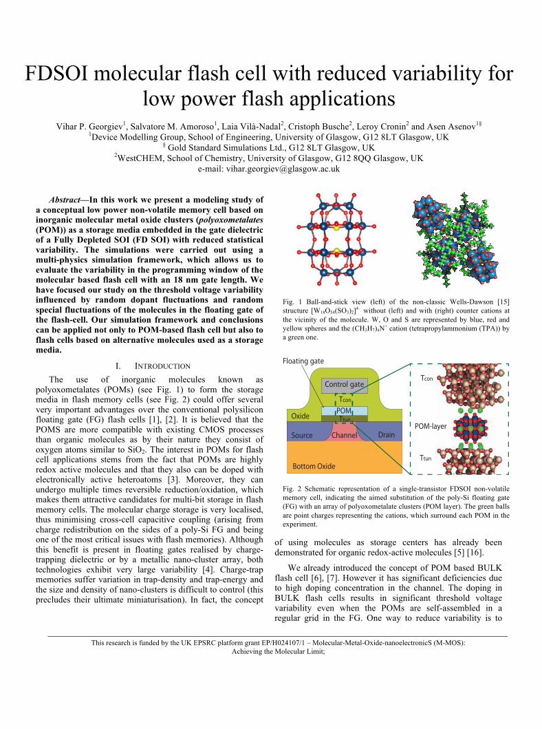
Fig. 2 Schematic representation of a single-transistor FDSOI non-volatile memory cell, indicating the aimed substitution of the poly-Si floating gate (FG) with an array of polyoxometalate clusters (POM layer). The green balls are point charges representing the cations, which surround each POM in the experiment.
Channel Source Drain
Control gate
Oxide
Floating gate
POMTcon
Ttun
Ttun
POM-layer
Tcon
ayer
Bottom Oxide
978-1-4799-4376-0/14/$31.00 ©2014 IEEE 353
introduce nonuniform channel doping - such as retrograde and δ-shape doping [8]. Another possibility for reducing the flash cell variability and to improve the device performance is to change the flash cell architecture and move from BULK to FDSOI. FDSOI architecture provides excellent electrostatic integrity, which tolerates low channel doping leading to very low native statistical variability. This is very important for low power applications, which is the holy grail of the modern flash cell technology.
Here, using 3D simulations, we compare the statistical variability of the threshold voltage of a BULK and FDSOI non-volatile flash-memory cell, in which the charge-storing components constitute a layer of polyoxometalate molecular clusters (POMs) (see Fig. 2). As a test case we constructed an 18nm-gate-length memory cell. Statistical variability arising from the random dopant fluctuations (RDF) and POM fluctuations (POMF) are also considered in the present study. The former known to be of largest impact in decananometer devices, the latter being anticipated due to POM-layer deposition or self-assembly.
II. FLASH CELL DESIGN The key design parameters of our template flash memory
cell are based on our recent publication [7]. For the purpose of this study, an n-channel FDSOI flash memory cell with an 18 nm square gate has been designed (Fig. 2). It is based on a previously studied 18 nm ‘template’ transistor [9] and is similar to the contemporary flash cells studied elsewhere [10].
Given that the gate area of the template flash cell is 18 x18 nm2, we consider sheet densities NS of POM clusters, approximately 2.8x1012 cm-2 corresponding to nine metal clusters arranged in a 3x3 rectangular planar grid. The control oxide thickness Tcon (see Fig. 2) is 15.6 nm. The tunneling oxide thickness Ttun, similarly to [6], [7], consists of a 3 nm high-quality SiO2. The [W18O54(SO3)2]4- POM layer thickness is 3 nm, including the balancing cations, (CH3H7)4N+ (tetrapropyl-ammonium (TPA)). The molecule its self is negatively charged and, in order to keep the entire system neutral, in the experiment each POM is surrounded by positively charged molecules (cations – green structure in Fig. 1). Together they form an insulating barrier of permittivity very close to that of SiO2 [11]. The POMs are oriented parallel to the SiO2 surfaces. All simulations are performed at low drain bias (VDS = 50 mV).
III. SIMULATION METHODOLOGY In order to evaluate the performance of POMs as storage
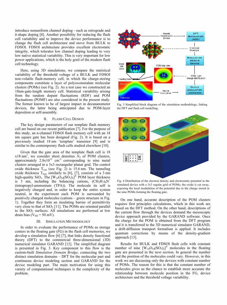
centers in the floating gate (FG) in the flash cell memories, we develop a simulation flow [6] [7], that links density functional theory (DFT) to the commercial three-dimensional (3D) numerical simulator GARAND [12]. The simplified diagram is presented in Fig. 3. Key component to this flow is the custom-built Simulation Domain Bridge, connecting the two distinct simulation domains – DFT for the molecular part and continuous device modeling section and GARAND for the device modeling part. The main motivation for using this variety of computational techniques is the complexity of the problem.
On one hand, accurate description of the POM clusters requires first principles calculations, which in this work are based on the DFT method. On the other hand, descriptions of the current flow through the devices demand the mesoscopic device approach provided by the GARAND software. Once the charge for the POM is obtained from the DFT program and it is transferred to the 3D numerical simulator GARAND, a drift-diffusion transport formalism is applied. It includes quantum corrections by means of the density-gradient approach [13].
Results for BULK and FDSOI flash cells with constant number of nine [W18O54(SO3)2]4- molecules in the floating gate are presented in the next section. In general the number and the position of the molecules could vary. However, in this work we are discussing only the devices with constant number of POMs. The reason for this is that the constant number of molecules gives us the chance to establish more accurate the relationship between molecule position in the FG, device architecture and the threshold voltage variability.
Fig. 3 Simplified block diagram of the simulation methodology, linking the DFT and flash cell modelling.
Fig. 4 Distribution of the electron density and electrostatic potential in the simulated device with a 3x3 regular grid of POMs; the oxide is cut away, exposing the local modulation of the potential due to the charge stored in the nine POMs forming the floating gate.
354

IV. STATISTICAL VARIABILITY In order to obtain realistic results for threshold voltage variability in FDSOI and BULK flash cell with POM molecules as a storage media, we introduce three sets of 2000 devices. Each set has two sources of statistical variability, such as random dopant fluctuations (RDF) and POMs fluctuations (POMF). We incorporated the charge density of nine [W18O54(SO3)2]4- POMs (shown in Fig. 1) as a charge storage center. It should be emphasised that for all three sets of 2000 devices composing the ensembles, the number of POMs is constant and it equals nine. In the case of the RDF only calculations, the charge storage clusters are arranged in a regular grid of 3x3 POMs centered within the gate - Fig. 4. In the POMF only calculations, the molecules are randomly displaced laterally in relation to the regular 3x3 grid used previously. Finally, in the third case, both of these variations are included, i.e., RDF and POMF.
Three distinct VT values related to the three easily accessible redox states of the molecular cluster can be obtained. They are presented in Table I as follows: parent (neutral) POMs – no charge in the clusters. In 1x red. state – each POMs have one electron more in comparison to the parent molecule. Hence, the total number of charge in the floating gate is equal to -9q (q=charge of an electron). In 2x red. state – each POMs have two electrons more in comparison to parent cluster, corresponding to total number of -18q charges in the floating gate.
Table I and Table II present the statistics of an average value (µ) and the standard deviation (σ) of three different VT values for three different cases: devices with only random dopants present (RDF only), transistors with only POMs fluctuation present (POMF only) and cells with the combined RDF and POMF (RDF+POMF) for BULK and FDSOI correspondingly. All results are compared to the nominal values of the flash cell with continuous doping.
Fig. 5, Fig. 6 and Fig. 7 present the same data from Table I and Table II but in a graphical form. Each figure shows the probability density function (PDF) for an ensemble of 2000 devices with RDF only, POMF only and RDF + POMF correspondingly. Based on our numerical calculations displayed above we can draw the following important conclusions.
Firstly, probability density (PDF) of the VT distribution for each bit in Fig. 5 – Fig. 7 shows significant different behaviour comparing FDSOI and BULK flash cells. In FDSOI devices PDFs are well separated and no overlap is observed. On contrary to FDSOI in BULK transistors the VT distribution shows significant overlap even before 1σ is reached in the case of RDF only and POMF+RDF. Those results prove the point that the doping in BULK flash cells results in significant threshold voltage variability even when the POMs are self-assembled in a regular grid in the floating gate. As we expected, FDSOI architecture exhibits lower correlation between sources of statistical variability and device performance which is very good news for low power application.
TABLE I. NOMINAL THRESHOLD VOLTAGE OF BULK THE CELL ENCODING 3 BITS AND THE CORRESPONDING AVERAGE AND STANDARD DEVIATION
VALUES FOR THE THREE ENSEMBLES WITH VARIABILITY.
Bit Nomi-nal VT
RDF 2000 devices
POMF 2000 devices
RDF+POMF 2000 devices
(Hex) redox state
VT VT σVT VT σVT VT σVT
(V) (V) (mV) (V) (mV) (V) (mV) (1) parent 1.778 1.821 448 1.778 0 1.820 449 (2) 1x red. 2.948 2.976 443 2.945 42 2.974 446 (3) 2x red. 4.107 4.122 437 4.089 92 4.113 453
Fig. 5 Probability density function (PDF) of the VT distribution for each bit of 2000 FDSOI (left) and BULK (right) devices with RDF only. Dashed line is a Gaussian fit.
Fig. 6 Probability density function (PDF) of the VT distribution for each bit of 2000 FDSOI (left) and BULK (right) devices POMF only.
Fig. 7 Probability density function (PDF) of the VT distribution for each bit of FDSOI (left) and BULK (right) devices with combined variability (RDF with POMF).
TABLE II. NOMINAL THRESHOLD VOLTAGE OF THE FDSOI CELL, ENCODING 3 BITS FOR CONTINUOUS FLASH; CORRESPONDING AVERAGE AND STANDARD
DEVIATION VALUES FOR THE THREE ENSEMBLES WITH VARIABILITY.
Bit Nomi-nal VT
RDF 2000 devices
POMF 2000 devices
RDF+POMF 2000 devices
(Hex) redox state
VT VT σVT VT σVT VT σVT
(V) (V) (mV) (V) (mV) (V) (mV) (1) parent -0.056 -0.052 98 -0.129 0 -0.052 92 (2) 1x red. 0.902 0.784 84 0.716 37 0.786 91 (3) 2x red. 1.743 1.615 77 1.546 73 1.610 105
0 1 2
Threshold Voltage VT(V)
10−3
10−2
10−1
100
101
Pro
bab
ilit
yden
sity
parent1x red.2x red.
0 1 2 3 4 5 6
Threshold Voltage VT(V)
10−3
10−2
10−1
100
Pro
bab
ilit
yden
sity
parent1x red.2x red.
0 1 2
Threshold Voltage VT(V)
10−3
10−2
10−1
100
101
Pro
bab
ilit
yden
sity
parent1x red.2x red.
0 1 2 3 4 5 6
Threshold Voltage VT(V)
10−3
10−2
10−1
100
101
Pro
bab
ilit
yden
sity
parent1x red.2x red.
0 1 2
Threshold Voltage VT(V)
10−3
10−2
10−1
100
101
Pro
bab
ilit
yden
sity
parent1x red.2x red.
0 1 2 3 4 5 6
Threshold Voltage VT(V)
10−3
10−2
10−1
100
Pro
bab
ilit
yden
sity
parent1x red.2x red.
355

Secondly, the curves presenting the PDF for all devices with RDF (Fig. 5 and Fig. 7) are broader in comparison to the POMFs only case (Fig. 6). This reflects the values of the standard deviation shown in the tables where all FDSOI (BULK) flash cells with RDF+POMF have standard deviation of around 100 mV (450mV), while in the case of the POMF only calculations this value varies from 0 to 73 mV (0 to 92 mV). Moreover, in the case FDSOI (BULK) of RDF-only calculations σVT varies from 77 to 98 mV (from 437 to 448 mV), placing it between the other two scenarios. Hence, it can be concluded that the RDF has stronger impact on the σVT in comparison to the POMF only scenario. Additionally, the two sources of variability show similar behaviour and the main source of variability is indeed the RDF. Also, in all calculations the results fit well a Gaussian distribution (dashed line in Fig. 5 – Fig. 7) except for the tails of the curves. Such a discrepancy between analytical approximations and numerical calculations emphasises the importance of numerical simulation in determining the devices’ performance.
Thirdly, for the FDSOI continuous doping structures the average value of VT for each bit has higher values in comparison to the average values of VT for the RDF only, POMF and RDF+POMF cells. In two cases, RDF and RDF+POMF, we observe almost identical values of VT. However, the standard deviation decreases in the RDF cells with increasing of the redox state of the molecule. The same is valid not only for the FDSOI but BULK flash cells. This effect occurs due to an increasing control of the storage charge over the charge conductance. σVT for the POMF only transistors shows opposite effect. σVT increases with the increase of the negative charge in the POM. However, this reflects a known dependence of variance of the number of charges in the oxide [14]. This dependence is much stronger and it is reflected in the RDF+POMF ensemble too.
Last but not least, in the case of the continuous doped FDSOI device the average value of VT, needed for the cell to change the oxidation state by one electron for each POM is 0.96 V and 0.84 V. In the case of the RDF, POMF RDF+POMF structures the VT steps are almost identical and they are around 0.84 V and 0.83V for the first and the second step of oxidation, respectively. The average values of ΔVT, for the BULK transitions from parent to 1x reduced and 2x reduced states, are approximately 1.16 V for the RDF, POMF and RDF+POMF ensembles, which compares very well with the 1.17 V nominal window separating the bits, as deduced from Table I. Hence, there appears to be almost negligible degradation of the average programming window for FDSOI and BULK devices with sources of statistical variability in comparison to the continuous cells.
V. CONCLUSION In this paper we compare the statistical threshold voltage
variability of a molecular based the 18-nm FDSOI and BULK flash cells. We introduced two sources of statistical variability such as RDF and POMF. Also, we established which source of variability is more influential for the statistics of VT. Our work showed that our approach provides both qualitative and quantitate inside toward the design and optimisation of such molecular-based flash cell, particularly in the context of
sources of statistical variability. Most importantly, the use of FDSOI cell architecture reduces significantly the threshold voltage variability in comparison to the BULK flash cell transistors. In the future we will concentrate our efforts to close the circle between creating physical devices, flash cell design and chemical synthesis.
REFERENCES [1] J. Lee et al., “Effects of floating-gate interference on NAND flash
memory cell operation”, IEEE Electron Device Letters, vol. 23, no. 5, pp. 264, 2002.
[2] J. Shaw et al., “Integration of self-assembled redox molecules in flash memories”, IEEE Trans. Electron Devices, vol.58, no. 3, pp. 826, 2011.
[3] D.-L. Long et al, “Confined electron transfer reactions within a molecular metal oxide 'trojan horse'“, Angew. Chem. Int. Ed., vol. 44, pp. 3415, 2005.
[4] S. M. Amoroso et al. “3D Monte Carlo simulation of the programming dynamics and their statistical variability in nanoscale charge-trap memories”, IEDM 2010 Tech Digest, pp. 22.6.1-22.6.4
[5] J. Shaw et al., “Redox molecules for a resonant tunnelling barrier in non-volatile memory”, IEEE Trans. Electron Devices, vol.59, no. 4, pp. 1189, 2012.
[6] L. Vilà-Nadal et al., “Towards polyoxometalate-cluster-based nano-electronics”, Chem. Eur. J., vol. 19, no. 49, pp. 16502-16511, 2013.
[7] V. Georgiev et al., “Optimisation and evaluation of variability in the programming window of a flash cell with molecular metal-oxide storage”, IEEE Trans. Electron Devices, in press, DOI: 10.1109/TED.2014.2315520.
[8] A. Ghetti et al., “Impact of nonuniform doping on random telegraph noise in flash memory devices”, IEEE Trans. Electron Devices, vol. 59, no. 2, pp. 309-315, 2012.
[9] S. Markov et al., “Drain Current Collapse in Nanoscaled Bulk MOSTETs Due to Random Dopant Compensation in the Source/Drain Extensions”, IEEE Trans. Electron Devices, vol. 58, no. 8, pp. 2385, 2011.
[10] S. M. Amoroso et al., “Three-dimensional simulation of charge-trap memory programming – Part II: Variability”, IEEE Trans. Electron Devices, vol. 58, no. 7, pp. 1864, 2011.
[11] N. Glezos et al., “Tunneling transport in polyoxometalate based composite materials”, Appl. Phys. Lett., vol. 83, no. 3, pp.488–490, 2003.
[12] http://www.GoldStandardSimulations.com.
[13] A. Asenov et al., “Increase in the random dopant induced threshold fluctuations and lowering in sub-100 nm MOSFETs due to quantum effects: a 3-D density-gradient simulation study”, IEEE Trans. Electron Devices, vol. 48, no. 4, pp. 722, 2001.
[14] S. Markov et al, “Statistical integration of multiple oxide traps under BTI stress of nanoscale MOSFETs”, IEEE Trans. Electron Devices, vol. 34, no. 5, pp. 686-688, 2013.
[15] N. Fay et al., “Structural, Electrochemical, and Spectroscopic Characterization of a Redox Pair of Sulfite-Based Polyoxotungstates: α-[W18O54(SO3)2]4- and α-[W18O54(SO3)2]5-”, Inorg. Chem., vol. 46, pp. 3502, 2007.
[16] S. Paydavosi et al., “High-density charge storage on molecular thin films - candidate materials for high storage capacity memory cells”, IEEE IEDM, 11-543, pp. 24-4-1, 2011.
356


![3D TCAD Model for Poly-Si Channel Current and ... - TU Wienin4.iue.tuwien.ac.at/pdfs/sispad2019/SISPAD_3.4.pdf · Variability in Vertical NAND Flash Memory ... [13]. The target dimensions](https://img.dokumen.tips/doc/110x75/605b4071c756e0407421c0c0/3d-tcad-model-for-poly-si-channel-current-and-tu-variability-in-vertical-nand.jpg)