Embed Size (px)
Citation preview
Experimental verification of the rainbow trappingeffect in adiabatic plasmonic gratingsQiaoqiang Gana,b,1, Yongkang Gaoa, Kyle Wagnerc, Dmitri Vezenovc, Yujie J. Dinga, and Filbert J. Bartolia,1
aCenter for Optical Technologies, Electrical and Computer Engineering Department, Lehigh University, Bethlehem, PA 18015; bElectrical EngineeringDepartment, University at Buffalo, The State University of New York, Buffalo, NY 14260; and cDepartment of Chemistry, Lehigh University, Bethlehem,PA 18015
Edited* by Erich P. Ippen, Massachusetts Institute of Technology, Cambridge, MA, and approved February 8, 2011 (received for review October 6, 2011)
We report the experimental observation of a trapped rainbowin adiabatically graded metallic gratings, designed to validatetheoretical predictions for this unique plasmonic structure. One-dimensional gradednanogratingswere fabricated and their surfacedispersion properties tailored by varying the grating groove depth,whose dimensions were confirmed by atomic force microscopy.Tunable plasmonic bandgaps were observed experimentally, anddirect optical measurements on graded grating structures showthat light of different wavelengths in the 500–700-nm region is“trapped” at different positions along the grating, consistent withcomputer simulations, thus verifying the “rainbow” trappingeffect.
slow light ∣ surface dispersion engineering ∣ surface plasmons
Since Ebbesen et al.’s report on extraordinary optical transmis-sion through plasmonic hole arrays was published in 1998 (1),
the study of plasmonics and metamaterials (2) has progressed at arapid pace and led to the discovery of phenomena with uniqueoptical properties. For example, recent theoretical investigationsreported the “trapped rainbow” storage of terahertz waves inmetamaterials (3) and plasmonic graded structures (4), and gen-erated considerable interest for slow-light applications. It waspredicted that tapered waveguides with a negative refractiveindex core (3) and graded metallic grating structures (4, 5) werecapable of slowing a broadband rainbow to a standstill. By varyingthe nanotopology of metal surfaces, the optical properties ofsurface plasmon polaritons (SPPs) can be tailored via so-calledsurface dispersion engineering (6–8). Moreover, by scaling thefeature size of the graded grating structures down to the nan-ometer scale, it was theoretically predicted that telecommunica-tion waves and even visible waves can also be trapped (9, 10).
The intrinsic slow-light properties of SPP modes in 1Dmetallicgrating structures can be seen from their dispersion relations,where their group velocity vg is found to decrease significantlyas the photonic band edge is approached. Our recent investiga-tions of simple 1D metallic gratings demonstrated that thesurface dispersion properties can be tuned by systematically vary-ing the groove depth and grating period. The dispersion relationsfor adiabatically graded gratings vary monotonically with posi-tion, so that incoming waves at different wavelengths can betrapped or localized at different positions along the propagationdirection of the grating.
Advances in nanofabrication and characterization techniquesnow permit the experimental demonstration of this interestingclass of structures. Rainbow trapping has not yet been unambigu-ously demonstrated in the visible regime for either metamaterials(3) or plasmonic structures (4, 5, 9), although in related studiesphotonic crystal nanocavities with graded hole size were recentlyshown to exhibit adiabatically reduced group velocities for photo-nic modes at telecommunication frequencies (11). Two prelimin-ary efforts were recently reported to realize the trapped rainbowin tapered metamaterial waveguides (12, 13). However, thereis currently no clear pathway for realizing negative refractive in-dices materials over a broad range of visible wavelengths (2, 14),as required for the tapered metamaterial waveguide concept (3).
On the other hand, the adiabatically graded plasmonic gratingsare convenient and practical structures that can be readily rea-lized by modern nanofabrication techniques. In the present work,one-dimensional adiabatically graded metallic grating structureswere designed, fabricated, and experimentally characterized.
The first part of this paper describes the tailoring of the surfacedispersion properties by tuning the nanopatterned groove depthand grating period. Experimental interferometric measurementsare performed to confirm key features of the theoretically pre-dicted SPP dispersion properties, including observation of thephotonic bandgap, and variation of the cutoff wavelength withgroove depth. Finally, rainbow trapping in graded grating struc-tures is experimentally demonstrated at room temperature inthe visible domain. Due to the large decrease in the SPP groupvelocity at a specific position along the adiabatic grating surface,the SPP modes are predicted to accumulate at this position (4, 9).Scattering from SPP modes propagating along the nanopatternedsurface permits probing of the localized intensity of the surface-confined SPP mode as a function of position by far-field opticalmicroscopy. These measurements confirm that SPP modes of dif-ferent wavelengths are localized at different positions along thegraded grating, thus validating the theoretical predictions of“rainbow trapping.” Such solid-state plasmonic slow-light struc-tures provide a means to control the group velocity (15), with thepotential for incorporation into light-based (photonic) logiccircuits.
Surface Dispersion Engineering of 1D Metallic GrooveArraysTo illustrate the tunability of the dispersion curves of nanopat-terned surfaces, angular-dependent reflection spectra of silvergrating surfaces were calculated using the rigorous coupled-waveanalysis (RCWA) method,* and their corresponding dispersioncurves are plotted in Fig. 1 for a series of groove depths. The grat-ing period and groove width are 520 and 150 nm, respectively.The calculated dispersion relations in the first Brillouin zoneexhibit a downward curvature relative to the free-space light lines,indicating a reduced vg for the SPP modes. Note that the vgreduction is greater for larger groove depths. Fig. 1 also showsthe surface photonic bandgap for these periodic nanopatterns(6–8), which is located roughly in the 540–560 nm wavelengthregion and broadens with increasing groove depth. SPP modesin this frequency region cannot be supported by this nanopat-terned surface. Such groove structures have been suggested as
Author contributions: Q.G. and F.J.B. designed research; Q.G., Y.G., K.W., and D.V.performed research; Q.G. and F.J.B. analyzed data; and Q.G., Y.J.D., and F.J.B. wrotethe paper.
The authors declare no conflict of interest.
*This Direct Submission article had a prearranged editor.
*RCWA simulation with the commercial solver, Diffraction mode (Rsoft, Inc.), is used tocalculate the reflection spectra of the silver grating structures.
1To whom correspondence may be addressed. E-mail: [email protected] or [email protected].
This article contains supporting information online at www.pnas.org/lookup/suppl/doi:10.1073/pnas.1014963108/-/DCSupplemental.
www.pnas.org/cgi/doi/10.1073/pnas.1014963108 PNAS ∣ March 29, 2011 ∣ vol. 108 ∣ no. 13 ∣ 5169–5173
APP
LIED
PHYS
ICAL
SCIENCE
S

a surface distributed Bragg reflector for a unidirectional surfacewave coupler (16) or a bidirectional plasmonic splitter (17, 18).Similar modeling also demonstrates how the shape of the disper-sion curves can be tailored by varying the grating period (SI Textand Fig. S1).
Experimental Verification of Surface Dispersion EngineeringTo confirm the above theoretical predictions of surface dispersionengineering experimentally, a series of 1D nanopatterned grat-ings with different groove depths were fabricated using focusion beam (FIB) milling (FEI Dual-Beam System 235). Eight grat-ings were fabricated on a 300-nm-thick layer of Ag that had beenevaporated onto flat fused silica microscope slides (Fisherbrand).The period and the width of this series of gratings were approxi-mately 520 and 150 nm, respectively. The eight structures havegroove depths of 4.7ð�0.2Þ, 6.8ð�0.1Þ, 9.1ð�0.2Þ, 11.7ð�0.5Þ,14.5ð�0.5Þ, 16.7ð�0.5Þ, 20.2ð�0.7Þ, and 23.9ð�0.9Þ nm as mea-sured by an atomic force microscope (AFM; Asylum ResearchMFP-3D) with an ultrasharp tip (NanoAndMore USA, Inc.,SSS-NCHAFM probes). SEM images of two gratings with groovedepths of approximately 4.7 and 23.9 nm are shown in Fig. 2.Next, two nanoslits were patterned on opposite sides of each grat-ing structure to function as the input and output couplers (19) fora plasmonic Mach–Zehnder interferometer (MZI) (20), as illu-strated in Fig. 3A. The slit separation distance for these samples isapproximate 21 μm. Both the top metal–glass interface 1 and bot-tom metal–air interface 2 can support SPP modes. When SPPmodes excited by the slit on the left propagate to the right slit,the SPP signals from the upper and lower optical branches inter-fere with each other and modulate the far-field distribution of thescattered waves. This plasmonic MZI permits experimental char-acterization of the optical properties of the surface grating struc-tures and validation of the predicted bandgaps as a function ofgroove depth.
Measurement of the modulated far-field transmission of theplasmonic MZI as a function of wavelength permits detectionof the SPP bandgap of the grating structure at the metal–air inter-face. Variations in the bandgap of SPP modes for different nano-patterend surfaces are detected from changes in their interferencepatterns. The onset of reductions in vg is also determined. Thefar-field interference pattern varies as (19) (see SI Text)
cos�2πLλ
ðneff1 − neff2Þ þ φ0
�; [1]
where neff is the effective refractive index of the metal–dielectricinterface, L is the slit separation distance, and φ0 is an additionalphase shift. For the flat interface 1, the effective refractive index isgiven by the expression
ffiffiffiffiffiffiffiffiffiffiffiffiffiffiffiffiffiffiffiffiffiffiε0mðλÞn21
ε0mðλÞ þ n21
s;
where ϵ0m is the real part of the metal permittivity, and n1 isthe refractive index of the substrate. For the nanopatternedinterface 2, neff2 changes with grating geometry.
The measured interference oscillations for the eight plasmonicMZIs are shown in Fig. 3B. In this data, the low-frequency back-ground and high-frequency noise have been numerically filteredusing a fast Fourier transform technique (with a low-frequencycutoff of approximately 4.344 μm−1 and high-frequency cutoffof approximately 101.358 μm−1). The observed interferenceoscillations in the 570–580-nm wavelength region decrease inamplitude and eventually disappear with increasing groove depth(as shown by the black arrow), indicating the presence of an SPPbandgap. The data show that the bandgap broadens as the groovedepth increases, consistent with theoretical predictions (19)(see Fig. S2). For grooves deeper than 10 nm, interference oscil-lations are not observed on the short wavelength side of the band-gap, because of the increased loss of SPP modes that are moretightly confined at these higher frequencies. To further confirmthe tunability of the SPP bandgap, a series of four structureswas also fabricated with grating period and groove width ofapproximately 635 and 200 nm, respectively. For these structures,the interference oscillations disappear between the wavelengthsof 660 and 700 nm as the groove depth increases, indicating a shiftof the bandgap to longer wavelengths (19) (see Fig. S3). Thesemeasurements provide clear evidence that the surface dispersionproperties can be tuned by tailoring the dimensions of the nano-patterned surface.
It is also possible to determine the group velocity vg2 and groupindex ngr ¼ c∕vg2 of the SPP modes at the nanopatterned air–Ag interface, by measuring the peak and valley wavelengths ofinterference oscillations. The derived group index at the metal–air interface increases up to 1.35 for nanopatterned surfaces inthe spectral region of 600–800 nm, as shown in Fig. S4 (19).Although this increase is modest, the data show that it occurs overa broad range of wavelengths and that the group index increaseswith increasing groove depth, as predicted. These experimentaldata demonstrate the broadband slowing of light in nanoengi-neered plasmonic structures. In principle, it should be possibleto determine significantly larger group indices, but that is difficultusing the current sample geometry (see Fig. S5). Although thegroup index increases as the groove depth increases, neff becomescloser for the two arms of the plasmonic MZI, increasing the per-iod of the interference pattern and making observation near theband edge more difficult (19) (see SI Text). Nevertheless, from thetheoretical simulation results in Fig. 1, one can estimate that thevg2 decreases to 0.01c at the band edge (here c is the light speed inthe free space).
Metallic Graded GratingsWe now discuss the fabrication and experimental characterizationof graded grating structures to verify the trapped rainbow effect,which is the primary focus of this paper. Employing the principlesof surface dispersion engineering discussed above, a graded grat-ing was designed for the 500–700-nm wavelength region, andfabricated by FIB milling, with a grating period and groove widthof approximately 475 and 150 nm, respectively (see Fig. 4A). Thesurface topology was measured by AFM. The milling time foreach successive groove was incrementally increased to achievea grating with a linearly graded groove depth. AFM measure-
Fig. 1. Dispersion curves of the nanopatterned silver gratings with groovedepths of 5, 10, 20, and 30 nm, calculated by the RCWA method. The dashedlines are light lines in free space. In these calculations, the period and widthof the grooves are 520 and 150 nm, respectively.
Fig. 2. SEM images of two gratings with groove depths of 4.7 and 23.9 nm.The period and the width of this series of gratings were approximately 520and 150 nm, respectively.
5170 ∣ www.pnas.org/cgi/doi/10.1073/pnas.1014963108 Gan et al.
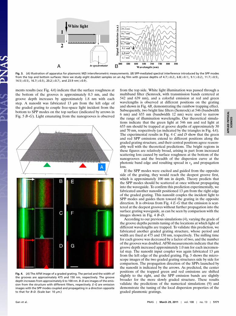
ments results (see Fig. 4A) indicate that the surface roughness atthe bottom of the grooves is approximately 0.3 nm, and thegroove depth increases by approximately 1.8 nm with eachstep. A nanoslit was fabricated 13 μm from the left edge ofthe graded grating to couple free-space light incident from thebottom to SPP modes on the top surface (indicated by arrows inFig. 5 B–G). Light emanating from the nanogrooves is observed
from the top side. White light illumination was passed through amultiband filter (Semrock, with transmission bands centered at542 and 639 nm), and a colorful emission at red and greenwavelengths is observed at different positions on the gratingand shown in Fig. 4B, demonstrating the rainbow trapping effect.Subsequently, two bright line filters (Semrock) at 546 (bandwidth6 nm) and 655 nm (bandwidth 12 nm) were used to narrowthe range of illumination wavelengths. Our theoretical simula-tions indicate that the green light at 546 nm and red light at655 nm should be trapped at groove depths of approximately 30and 70 nm, respectively (as indicated by the triangles in Fig. 4A).The experimental results in Fig. 4 C and D show that the greenand red SPP emissions extend to different positions along thegraded grating structure, and their central positions agree reason-ably well with the theoretical predictions. The bright regions inthese figures are relatively broad, arising in part from increasedscattering loss caused by surface roughness at the bottom of thenanogrooves and the breadth of the dispersion curve at thephotonic band edge and resulting spread in vg and propagationloss.
If the SPP modes were excited and guided from the oppositeside of the grating, they would reach the deepest groove first,which is approximately 100 nm in depth. Theory predicts thatthe SPP modes should be scattered at once without propagatinginto the waveguide. To confirm this prediction experimentally, wefabricated another nanoslit positioned 13 μm from the right edgeof the graded grating. This nanoslit couples the incident light toSPP modes and guides them toward the grating in the oppositedirection. It is obvious from Fig. 4 E–G that the emission is scat-tered at the deepest grooves without further propagation into thesurface grating waveguide, as can be seen by comparison with theimages shown in Fig. 4 B–D.
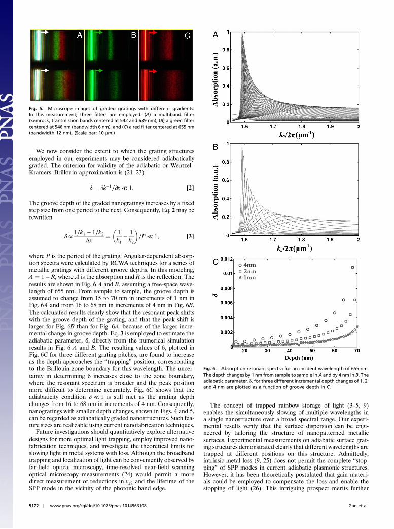
According to our previous simulations (4), varying the grade ofthe groove depths permits tuning of the locations at which light ofdifferent wavelengths are trapped. To validate this prediction, wefabricated another graded grating structure, whose period andwidth are fixed at 475 and 150 nm, respectively. The milling timefor each groove was decreased by a factor of two, and the numberof the grooves was doubled. AFMmeasurements indicate that thegroove depth increased approximately 1.0 nm for each incremen-tal step. The nanoslit input coupler was again fabricated 13 μmfrom the left edge of the graded grating. Fig. 5 shows the micro-scope images of the two graded grating structures side by side forcomparison. The propagation direction of the SPPs launched bythe nanoslit is indicated by the arrows. As predicted, the centerpositions of the trapped green and red emissions are shiftedslightly to the right, and the SPP emission bands are slightlybroader for the more slowly graded structure. These resultsvalidate the predictions of the numerical simulations (9) anddemonstrate the tuning of the local dispersion properties of thegraded plasmonic gratings.
Fig. 3. (A) Illustration of apparatus for plasmonic MZI interoferometric measurements. (B) SPP-mediated spectral interference introduced by the SPP modesfrom the top and bottom surfaces: Here we study eight doublet samples on an Ag film with groove depths of 4.7ð�0.2Þ, 6.8ð�0.1Þ, 9.1ð�0.2Þ, 11.7ð�0.5Þ,14.5ð�0.5Þ, 16.7ð�0.5Þ, 20.2ð�0.7Þ, and 23.9 nmð�0.9Þ.
Fig. 4. (A) The AFM image of a graded grating. The period and the width ofthe grooves are approximately 475 and 150 nm, respectively. The groovedepth increases from approximately 6 to 100 nm. B–D are images of the emis-sion from the structure with different filters, respectively. E–G are emissionimages with the SPP modes coupled and propagating in a direction oppositeto that for B–D. (Scale bar: 10 μm.)
Gan et al. PNAS ∣ March 29, 2011 ∣ vol. 108 ∣ no. 13 ∣ 5171
APP
LIED
PHYS
ICAL
SCIENCE
S
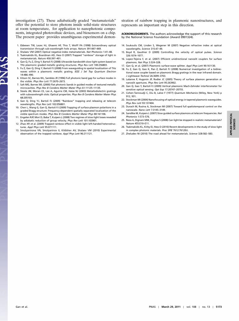
We now consider the extent to which the grating structuresemployed in our experiments may be considered adiabaticallygraded. The criterion for validity of the adiabatic or Wentzel–Kramers–Brillouin approximation is (21–23)
δ ¼ ∂k−1∕∂x ≪ 1. [2]
The groove depth of the graded nanogratings increases by a fixedstep size from one period to the next. Consequently, Eq. 2may berewritten
δ ≈1∕k1 − 1∕k2
Δx¼
�1
k1−
1
k2
�∕P ≪ 1; [3]
where P is the period of the grating. Angular-dependent absorp-tion spectra were calculated by RCWA techniques for a series ofmetallic gratings with different groove depths. In this modeling,A ¼ 1 − R, where A is the absorption and R is the reflection. Theresults are shown in Fig. 6 A and B, assuming a free-space wave-length of 655 nm. From sample to sample, the groove depth isassumed to change from 15 to 70 nm in increments of 1 nm inFig. 6A and from 16 to 68 nm in increments of 4 nm in Fig. 6B.The calculated results clearly show that the resonant peak shiftswith the groove depth of the grating, and that the peak shift islarger for Fig. 6B than for Fig. 6A, because of the larger incre-mental change in groove depth. Eq. 3 is employed to estimate theadiabatic parameter, δ, directly from the numerical simulationresults in Fig. 6 A and B. The resulting values of δ, plotted inFig. 6C for three different grating pitches, are found to increaseas the depth approaches the “trapping” position, correspondingto the Brillouin zone boundary for this wavelength. The uncer-tainty in determining δ increases close to the zone boundary,where the resonant spectrum is broader and the peak positionmore difficult to determine accurately. Fig. 6C shows that theadiabaticity condition δ ≪ 1 is still met as the grating depthchanges from 16 to 68 nm in increments of 4 nm. Consequently,nanogratings with smaller depth changes, shown in Figs. 4 and 5,can be regarded as adiabatically graded nanostructures. Such fea-ture sizes are realizable using current nanofabrication techniques.
Future investigations should quantitatively explore alternativedesigns for more optimal light trapping, employ improved nano-fabrication techniques, and investigate the theoretical limits forslowing light in metal systems with loss. Although the broadbandtrapping and localization of light can be conveniently observed byfar-field optical microscopy, time-resolved near-field scanningoptical microscopy measurements (24) would permit a moredirect measurement of reductions in vg2 and the lifetime of theSPP mode in the vicinity of the photonic band edge.
The concept of trapped rainbow storage of light (3–5, 9)enables the simultaneously slowing of multiple wavelengths ina single nanostructure over a broad spectral range. Our experi-mental results verify that the surface dispersion can be engi-neered by tailoring the structure of nanopatterned metallicsurfaces. Experimental measurements on adiabatic surface grat-ing structures demonstrated clearly that different wavelengths aretrapped at different positions on this structure. Admittedly,intrinsic metal loss (9, 25) does not permit the complete “stop-ping” of SPP modes in current adiabatic plasmonic structures.However, it has been theoretically postulated that gain materi-als could be employed to compensate the loss and enable thestopping of light (26). This intriguing prospect merits further
Fig. 5. Microscope images of graded gratings with different gradients.In this measurement, three filters are employed: (A) a multiband filter(Semrock, transmission bands centered at 542 and 639 nm), (B) a green filtercentered at 546 nm (bandwidth 6 nm), and (C) a red filter centered at 655 nm(bandwidth 12 nm). (Scale bar: 10 μm.)
Fig. 6. Absorption resonant spectra for an incident wavelength of 655 nm.The depth changes by 1 nm from sample to sample in A and by 4 nm in B. Theadiabatic parameter, δ, for three different incremental depth changes of 1, 2,and 4 nm are plotted as a function of groove depth in C.
5172 ∣ www.pnas.org/cgi/doi/10.1073/pnas.1014963108 Gan et al.
investigation (27). These adiabatically graded “metamaterials”offer the potential to store photons inside solid-state structuresat room temperature, for application to nanophotonic compo-nents, integrated photovoltaic devices, and biosensors on a chip.The present paper provides unambiguous experimental demon-
stration of rainbow trapping in plasmonic nanostructures, andrepresents an important step in this direction.
ACKNOWLEDGMENTS. The authors acknowledge the support of this researchby the National Science Foundation (Award 0901324).
1. Ebbesen TW, Lezec HJ, Ghaemi HF, Thio T, Wolff PA (1998) Extraordinary opticaltransmission through sub-wavelength hole arrays. Nature 391:667–669.
2. Shalaev VM (2007) Optical negative-index metamaterials. Nat Photonics 1:41–48.3. Tsakmakidis KL, Boardman AD, Hess O (2007) Trapped “rainbow” storage of light in
metamaterials. Nature 450:397–401.4. Gan Q, Fu Z, Ding Y, Bartoli FJ (2008) Ultrawide-bandwidth slow-light system based on
THz plasmonic graded metallic grating structures. Phys Rev Lett 100:256803.5. Fu Z, Gan Q, Ding Y, Bartoli FJ (2008) From waveguiding to spatial localization of THz
waves within a plasmonic metallic grating. IEEE J Sel Top Quantum Electron14:486–490.
6. Kitson SC, Barnes WL, Sambles JR (1996) Full photonic band gap for surface modes inthe visible. Phys Rev Lett 77:2670–2673.
7. Salt MG, Barnes WL (2000) Flat photonic bands in guided modes of textured metallicmicrocavities. Phys Rev B Condens Matter Mater Phys 61:11125–11135.
8. Steele JM, Moran CE, Lee A, Aguirre CM, Halas NJ (2003) Metallodielectric gratingswith subwavelength slots: Optical properties. Phys Rev B Condens Matter Mater Phys68:205103.
9. Gan Q, Ding YJ, Bartoli FJ (2009) “Rainbow” trapping and releasing at telecomwavelengths. Phys Rev Lett 102:056801.
10. Chen L, Wang G, Gan Q, Bartoli FJ (2009) Trapping of surface-plasmon polaritons in agraded Bragg structure: Frequency-dependent spatially separated localization of thevisible spectrum modes. Phys Rev B Condens Matter Mater Phys 80:161106.
11. Engelen RJP, Mori D, Baba T, Kuipers L (2008) Two regimes of slow-light losses revealedby adiabatic reduction of group velocity. Phys Rev Lett 101:103901.
12. Zhao XP, et al. (2009) Trapped rainbow effect in visible light left-handed heterostruc-tures. Appl Phys Lett 95:071111.
13. Smolyaninova VN, Smolyaninov II, Kildishev AV, Shalaev VM (2010) Experimentalobservation of the trapped rainbow. Appl Phys Lett 96:211121.
14. Soukoulis CM, Linden S, Wegener M (2007) Negative refractive index at opticalwavelengths. Science 315:47–49.
15. Boyd R, Gauthier D (2009) Controlling the velocity of optical pulses. Science326:1074–1077.
16. Lopez-Tejeira F, et al. (2007) Efficient unidirectional nanoslit couplers for surfaceplasmons. Nat Phys 3:324–328.
17. Gan Q, et al. (2007) Plasmonic surface-wave splitter. Appl Phys Lett 90:161130.18. Fu Z, Gan Q, Gao K, Pan Z, Bartoli FJ (2008) Numerical investigation of a bidirec-
tional wave coupler based on plasmonic Bragg gratings in the near infrared domain.J Lightwave Technol 26:3699–3703.
19. Lalanne P, Hugonin JP, Rodier JC (2005) Theory of surface plasmon generation atnanoslit apertures. Phys Rev Lett 95:263902.
20. Gan Q, Gao Y, Bartoli FJ (2009) Vertical plasmonic Mach-Zehnder interferometer forsensitive optical sensing. Opt Exp 17:20747–20755.
21. Cohen-Tannoudji C, Diu B, Laloe F (1977) Quantum Mechanics (Wiley, New York) p912, 931.
22. StockmanMI (2004) Nanofocusing of optical energy in tapered plasmonic waveguides.Phys Rev Lett 93:137404.
23. Durach M, Rusina A, Stockman MI (2007) Toward full spatiotemporal control on thenanoscale. Nano Lett 7:3145–3149.
24. SandtkeM, Kuipers L (2007) Slow guided surface plasmons at telecom frequencies.NatPhotonics 1:573–576.
25. Reza A, DignamMM, Hughes S (2008) Can light be stopped in realistic metamaterials?Nature 455:E10–E11.
26. Tsakmakidis KL, Kirby EI, Hess O (2010) Recent developments in the study of slow lightin complex photonic materials. Proc SPIE 7612:76120U.
27. Zheludev NI (2010) The road ahead for metamaterials. Science 328:582–583.
Gan et al. PNAS ∣ March 29, 2011 ∣ vol. 108 ∣ no. 13 ∣ 5173
APP
LIED
PHYS
ICAL
SCIENCE
S