Embed Size (px)
Citation preview

EVAL-ADAU1777Z User Guide UG-1055
One Technology Way • P.O. Box 9106 • Norwood, MA 02062-9106, U.S.A. • Tel: 781.329.4700 • Fax: 781.461.3113 • www.analog.com
Evaluating the ADAU1777 Four ADC, Two DAC, Low Power Codec
with Audio Processor
PLEASE SEE THE LAST PAGE FOR AN IMPORTANT WARNING AND LEGAL TERMS AND CONDITIONS. Rev. 0 | Page 1 of 25
EVALUATION KIT CONTENTS EVAL-ADAU1777Z evaluation board EVAL-ADUSB2EBZ (USBi) communications adapter USB cable with mini-B plug Evaluation board/software quick start guide
DOCUMENTS NEEDED ADAU1777 data sheet AN-1006 Application Note
GENERAL DESCRIPTION This user guide explains the design and setup of the EVAL-ADAU1777Z evaluation board.
This evaluation board provides full access to all analog and digital inputs/outputs on the ADAU1777. The ADAU1777 core is controlled by Analog Devices, Inc., SigmaStudio™ software, which interfaces to the board via a USB connection. The EVAL-ADAU1777Z can be powered by a single AAA battery, by the USB bus, or by a single 3.8 V to 5.5 V supply; any of these supplies are regulated to the voltages required on the board. The printed circuit board (PCB) is a 4-layer design, with a single ground plane and a single power plane on the inner layers. The board contains connectors for external microphones and speakers. The master clock can be provided externally or by the on-board 12.288 MHz passive crystal.
EVALUATION BOARD TOP SIDE
1505
4-00
1
Figure 1. EVAL-ADAU1777Z Top Side Assembly

UG-1055 EVAL-ADAU1777Z User Guide
Rev. 0 | Page 2 of 25
TABLE OF CONTENTS Evaluation Kit Contents ................................................................... 1 Documents Needed .......................................................................... 1 General Description ......................................................................... 1 Evaluation Board Top Side .............................................................. 1 Revision History ............................................................................... 2 Evaluation Board Block Diagrams ................................................. 3 Setting Up the Evaluation Board .................................................... 5
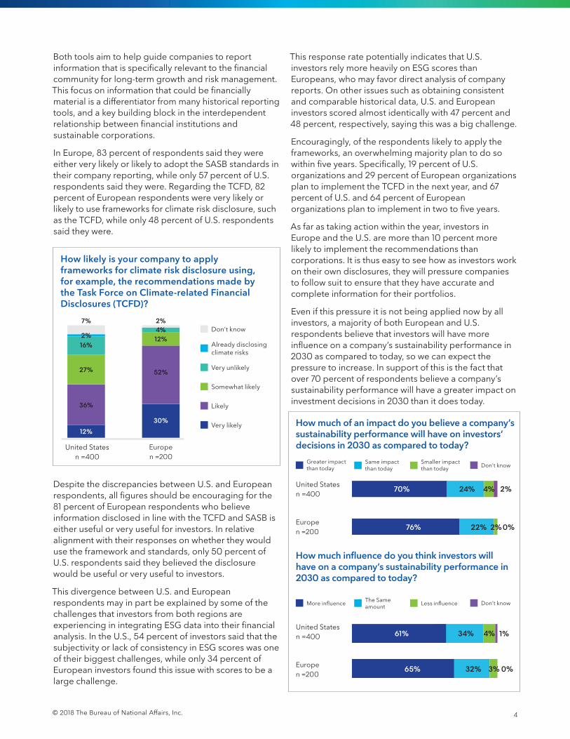
Installing the SigmaStudio Software .......................................... 5 Installing the USBi (EVAL-ADUSB2EBZ) Drivers.................. 5 Default Switch and Jumper Settings .......................................... 7 Powering Up the Board ............................................................... 7 Connecting the Audio Cables ..................................................... 7 Setting Up Communications in SigmaStudio ........................... 7 Creating a Basic Signal Flow ....................................................... 8 Downloading the Program to the DSP .................................... 10
Using the Evaluation Board .......................................................... 11 Power............................................................................................ 11 Inputs and Outputs .................................................................... 11 MP Pins........................................................................................ 13 Serial Audio Interface ................................................................ 13 Communications Header (J1) .................................................. 14 Self-Boot ...................................................................................... 14 Power-Down ............................................................................... 15
Hardware Description.................................................................... 16 Jumpers ........................................................................................ 16 Integrated Circuits (ICs) ........................................................... 16 LED .............................................................................................. 16
Evaluation Board Schematics and Artwork ................................ 17 Ordering Information .................................................................... 24
Bill of Materials ........................................................................... 24
REVISION HISTORY 12/2016—Revision 0: Initial Version

EVAL-ADAU1777Z User Guide UG-1055
Rev. 0 | Page 3 of 25
EVALUATION BOARD BLOCK DIAGRAMS
OSC
POWERSUPPLY
REGULATION
POWER/BYPASSSWITCH
I2C/SPICOMMUNICATIONS
HEADER
SELF-BOOTEEPROM
ANALOG MICINPUTS
STEREO LINEINPUT
DIGITAL MICINPUTS
SERIAL AUDIOCONNECTOR
MPPINS
DIFFERENTIALSTEREO OUTPUT
SINGLE-ENDEDSTEREO OUTPUT
XTALOSCILLATOR
MASTERCLOCK
ADAU1777
1505
4-00
2
Figure 2. Functional Block Diagram
1505
4-00
3
POWER/BYPASS SWITCH
POWER SUPPLY
DIFFERENTIAL/STEREO OUTPUTS EEPROM
OSC
SERIAL AUDIOCONNECTOR
MULTIPURPOSE PINS
PDM DMICHEADERS
I2C/SPIHEADER
SELF-BOOTSWITCH
ANALOG INPUTS
ADAU1777
STEREOANALOG
IN
Figure 3. Board Layout Block Diagram

UG-1055 EVAL-ADAU1777Z User Guide
Rev. 0 | Page 4 of 25
1505
4-00
4
Figure 4. Default Jumper and Switch Settings (Solid Black Rectangle Indicates a Switch or Jumper Position)
EVAL-ADAU1777Z User Guide UG-1055
Rev. 0 | Page 5 of 25
SETTING UP THE EVALUATION BOARD INSTALLING THE SigmaStudio SOFTWARE Download and install the latest version of SigmaStudio by completing the following steps:
1. Install the latest version of Microsoft® .NET Framework if it is not already installed on the PC. The latest version of the .NET Framework can be downloaded from the Microsoft website.
2. Go to www.analog.com/SigmaStudio and download the latest version of SigmaStudio from the Downloads and Related Products section.
3. Log in to your myAnalog account. (If you do not have an account, go to www.analog.com/MyAnalog, click Log In, and then click Register to create a new account.)
4. Fill in the download form and choose SigmaDSP as the target hardware.
5. Download the installer and execute the executable. Follow the prompts, including accepting the license agreement, to install the software.
INSTALLING THE USBi (EVAL-ADUSB2EBZ) DRIVERS SigmaStudio must be installed to use the USB interface (USBi). After the SigmaStudio installation is complete,
1. Connect the USBi to an available USB 2.0 port using the USB cable included in the evaluation board kit. (The USBi does not function properly with a USB 3.0 port.)
2. Install the driver software (see the Using Windows XP section or the Using Windows 7 or Windows Vista section for more information).
Using Windows XP
After connecting the USBi to the USB 2.0 port, Windows® XP recognizes the device (see Figure 5) and prompts the user to install the drivers.
1505
4-00
5
Figure 5. Found New Hardware Notification
1. From the Found New Hardware Wizard window, select the Install from a list or specific location (Advanced) option and click Next (see Figure 6).
1505
4-00
6
Figure 6. Found New Hardware Wizard—Installation
2. Select Search for the best driver in these locations, select Include this location in the search, and click Browse to find the USB drivers subdirectory within the SigmaStudio directory (see Figure 7).
1505
4-00
7
Figure 7. Found New Hardware Wizard—Search and Installation Options

UG-1055 EVAL-ADAU1777Z User Guide
Rev. 0 | Page 6 of 25
3. When the Hardware Installation warning appears, click Continue Anyway (see Figure 8).
1505
4-00
8
Figure 8. Hardware Installation Warning
The USBi drivers are now installed. Leave the USBi connected to the PC.
Using Windows 7 or Windows Vista
After connecting the USBi to the USB 2.0 port, Windows 7 or Windows Vista recognizes the device and installs the drivers automatically (see Figure 9). After the installation is complete, leave the USBi connected to the PC.
1505
4-00
9
Figure 9. USBi Drivers Installed Correctly
Confirming Proper Installation of the USBi Drivers
To confirm that the USBi drivers have been installed properly,
1. With the USBi still connected to the USB 2.0 port of the PC, check that both the yellow I2C LED and the red power indicator LED are illuminated (see Figure 10).
1505
4-01
0
Figure 10. State of USBi Status LEDs After Driver Installation
2. In Windows Device Manager, under the Universal Serial Bus controllers section, check that Analog Devices USBi (programmed) appears as shown in Figure 11.
1505
4-01
1
Figure 11. Confirming Driver Installation Using the Device Manager

EVAL-ADAU1777Z User Guide UG-1055
Rev. 0 | Page 7 of 25
DEFAULT SWITCH AND JUMPER SETTINGS The J8, J10, J12, and J17 jumpers must be connected to provide power to the ADAU1777, and the J3 jumper must be set to the USB/EXT power setting. The MP pin jumpers (J9) can be connected as desired to use the MP push-buttons or switches. The microphone bias jumpers, J11 and J14, can be connected if microphone bias is needed on the AIN0 and/or AIN1 inputs.
Switch S7 selects whether the board is to be powered up or if audio is to be bypassed from input to output with the board powered down. For normal operation, slide the switch to the left. S1 selects whether the ADAU1777 is powered from 3.3 V or 1.8 V; the default is 3.3 V. If powering the board via the USBi, ensure that the switch on the bottom of the USBi board is set to the correct voltage (1.8 V or 3.3 V). S2 controls the self-boot operation. By default, S2 is slid down to disable self-boot operation.
The following is an example setup for using the EVAL-ADAU1777Z analog stereo in to analog stereo out operation.
POWERING UP THE BOARD To power up the evaluation board, connect the ribbon cable of the USBi to J1 (control port) of the EVAL-ADAU1777Z.
CONNECTING THE AUDIO CABLES Connect a stereo audio source to J22 (AIN2/3). Connect headphones or powered speakers to J23 (stereo output).
1505
4-01
2
Figure 12. Stereo Out (J23) and Stereo In (J22)
SETTING UP COMMUNICATIONS IN SigmaStudio Start SigmaStudio by double-clicking the shortcut on the desktop.
Click File…New Project or press Ctrl+N to create a new project. The default view of the new project is the Hardware Configuration tab.
To use the USBi in conjunction with SigmaStudio, go to the Communication Channels subsection of the toolbox on the left side of the Hardware Configuration tab, select USBi, and click and drag it to the right to add it to the project space (see Figure 13).
1505
4-01
3
Figure 13. Adding the USBi Communication Channel
If SigmaStudio cannot detect the USBi on the USB port of the PC, the background of the USB label is red (see Figure 14). This can occur when the USBi is not connected or when the drivers are incorrectly installed.
1505
4-01
4
Figure 14. USBi Not Detected by SigmaStudio
If SigmaStudio detects the USBi on the USB port of the PC, the background of the USB label changes to green (see Figure 15).
1505
4-01
5
Figure 15. USBi Detected by SigmaStudio
To add an ADAU1777 to the project, select ADAU1777 from the Processors (ICs / DSPs) list, and drag it to the project space (see Figure 16).

UG-1055 EVAL-ADAU1777Z User Guide
Rev. 0 | Page 8 of 25
1505
4-01
6
Figure 16. Adding an ADAU1777
To use the USB interface to communicate with the target integrated circuit (IC), connect it by clicking and dragging a wire between the blue pin of the USBi and the green pin of the IC (see Figure 17). The corresponding drop-down box of the USBi automatically fills with the default mode and channel for that IC.
1505
4-01
7
Figure 17. Connecting the USB Interface to an ADAU1777 IC
CREATING A BASIC SIGNAL FLOW To access the Schematic tab, where a signal processing flow can be created, click the Schematic tab at the top of the screen (see Figure 18).
1505
4-01
8
Figure 18. Schematic Tab
The left side of the schematic view includes the Toolbox, which contains all of the algorithms that can run in the SigmaDSP. From within the IO > Audio Input > Pair 2 folder, select the Input cell (see Figure 19).
1505
4-01
9
Figure 19. Input Cell Selection
Click and drag the Input cell into the blank schematic space to the right of the Toolbox (see Figure 20).
1505
4-02
0
Figure 20. Input Cell
Go to the IO > Audio Output folder and select the Output cell (see Figure 21).
1505
4-02
1
Figure 21. Output Cell Selection
Click and drag an output cell to the schematic. Repeat this step to create two outputs (see Figure 22). Make sure that the output cells are assigned to OUT0 and OUT1, respectively.
1505
4-02
2
Figure 22. Output Cells
Connect the cells together by clicking a blue output dot and dragging to the green output dot of the next cell, connecting the Input 2 to OUT0 and Input 3 to OUT1 (see Figure 23).
1505
4-02
3
Figure 23. Connected Signal Flow
The basic signal flow is now complete with the stereo input/output.

EVAL-ADAU1777Z User Guide UG-1055
Rev. 0 | Page 9 of 25
Add Volume Control
To add volume control via the VOL− and VOL+ buttons, add jumpers to S6 and S4 on J9 (see Figure 24).
1505
4-02
4
Figure 24. Jumpers for Volume Push-Buttons
Go to the Hardware Configuration tab. In the bottom left corner, click the IC 1 – ADAU1777 Register Control tab (see Figure 25).
1505
4-02
5
Figure 25. IC 1 - ADAU1777 Register Control Tab
Find the Output/Serial Port tab in the top right corner. In the bottom left corner of the Output/Serial Port tab, the Push Button Vol section is located. Locate the drop-down box for Converters Controlled by PushButton Volume: and change its value to All ADCs (see Figure 26).
1505
4-02
6
Figure 26. Output/Serial Port Tab
Go to the Pin/Pad Control tab. In the Pin Modes section, change the value of DAC_SDATA/MP0 to Push-button volume down, and change the value of ADC_SDATA0/PDMOUT/MP1 to Push-button volume up (see Figure 27).
1505
4-02
7
Figure 27. Pin/Pad Control Tab
The schematic is ready to be compiled and downloaded to the evaluation board.

UG-1055 EVAL-ADAU1777Z User Guide
Rev. 0 | Page 10 of 25
DOWNLOADING THE PROGRAM TO THE DSP To compile and download the code to the DSP, click Link-Compile-Download in the main toolbar of SigmaStudio (see Figure 28). Alternately, press the F7 key.
1505
4-02
8
Figure 28. Link-Compile-Download
If the project does not compile correctly, an error displays (see Figure 29). If an error displays, return to SigmaStudio and check the configuration for mistakes.
When the project compiles, the signal flow runs on the evaluation board, and the audio passes from the input to the output. The volume can be changed in real time by using the buttons on the board.
1505
4-02
9
Figure 29. Compile Error

EVAL-ADAU1777Z User Guide UG-1055
Rev. 0 | Page 11 of 25
USING THE EVALUATION BOARD POWER Power can be supplied to the EVAL-ADAU1777Z in one of three ways. When Jumper J3 is in the USB/EXT position, power can be supplied by connecting the EVAL-ADUSB2EBZ (USBi) board to J1 (see Figure 30) or by connecting a 3.8 V dc to 5.5 V dc power supply to J2 (tip positive).
1505
4-03
0
Figure 30. Header J1, Control Port
To supply power via a 1.5 V battery, J3 must be set to the BATT position, and the battery must be connected to J5. The on-board regulator generates the 3.3 V dc or 1.8 V dc supply, determined by S1, for the on-board circuitry. LED D1 lights up when power is supplied to the board. To connect power to the ADAU1777, connect the J8, J10, J12, and J17 jumpers (see Figure 31).
1505
4-03
1
Figure 31. Power Jumpers
INPUTS AND OUTPUTS The EVAL-ADAU1777Z has multiple audio input and output options, including digital and analog. There are four single-ended analog inputs that are configurable as microphone or line inputs, dual stereo digital microphone inputs, and two differential outputs that can also be used in a single-ended configuration.
Analog Microphone Inputs
For microphone signals, the ADAU1777 analog inputs can be configured as single-ended inputs with optional programmable gain amplifier (PGA) mode.
Microphone Bias
To add MBIAS0 to AIN0, connect a jumper to the J11 header. Similarly, MBIAS1 or MBIAS0 can be added to AIN1 by connecting a jumper to the J14 header (see Figure 32).
1505
4-03
2
Figure 32. Microphone Bias Headers
Enable the microphone bias circuitry in the PGA/ADC tab of SigmaStudio. The appropriate gain settings can also be chosen via this tab (see Figure 33).
1505
4-03
3
Figure 33. Microphone Bias Enable and Gain
Stereo Line Input
The J22 stereo input jack accepts a standard stereo TRS 3.5 mm mini plug (tip is left, ring is right) with two channels of audio.

UG-1055 EVAL-ADAU1777Z User Guide
Rev. 0 | Page 12 of 25
Digital Microphones
Pulse density modulation (PDM) digital microphones can be connected to standard 0.100” headers (J6 and J7). To use the digital microphone headers on the EVAL-ADAU1777Z, ensure that the proper settings have been chosen in SigmaStudio. Go to the Pin/Pad Control tab (found in the Hardware Configuration/ ADAU1777 Register Control section). In the CLKOUT/ ADC_SDATA1/MP6 drop-down box, select Clock Output (see Figure 34).
1505
4-03
4
Figure 34. MP6, Clock Output
To set the value of BCLK, go to the PLL & Clock Control tab and change the value of the Output Clock Frequency drop-down box to the desired division on MCLK (see Figure 35).
1505
4-03
5
To:Self-bootXTAL
To: MainBlocks
CLOCKOUT
Figure 35. Clock Output Enabled/Divided
Set the input of the ADAU1777 to be the digital microphones instead of the ADCs by toggling the appropriate Decimator Source settings. Go to the PGA/ADC tab to find and set the following switches (see Figure 36).
The digital microphones can now be routed via the appropriate inputs on the Audio Input cell.
1505
4-03
6
Figure 36. Decimator Source
Headphone Output
The headphone output, J23, connects to any standard 3.5 mm mini plug stereo headphones. By setting the HP_EN_L and HP_EN_R bits in the headphone line output select register (Address 0x0043), the output pins can be driven either by a line output driver or by a headphone driver. Headphones can be driven either single-ended or differentially, and bits are available to disable the LN and RN pins if using single-ended.
Line Outputs
The J19 and J21 analog output pins can drive differential loads. In their default settings, these pins can drive line loads of 10 kΩ or greater.
To use an external speaker, solder wires to the unpopulated header pads, J13 and J16 (see Figure 37).
1505
4-03
7
Figure 37. Unpopulated J13 and J16 Headers

EVAL-ADAU1777Z User Guide UG-1055
Rev. 0 | Page 13 of 25
PDM Modulator Output
The ADAU1777 has a 2-channel PDM modulator. The PDM output and clock source are both located on the MP pins. To use this functionality, set ADC_SDATA0/PDMOUT/MP1 to PDM Modulator Output and set CLKOUT/ADC_SDATA1/MP6 to Clock Output. These settings can be found in the Pin/Pad Control tab (see Figure 38).
1505
4-03
8
Figure 38. PDM Modulator Output and Clock Output
The clock output is located on the J4 header, Pin 12. The PDM output is located on the J4 header, Pin 10 (see Figure 39).
1505
4-03
9
PDM OUTPUT CLOCK OUT Figure 39. PDM Output and Clock Output Pins
MP PINS The MP pin jumpers, Header J9, provide access to the MP pins (MP0, MP1, MP2, MP3, and MP6) of the ADAU1777, as well as facilitate the use of the push-buttons on the EVAL-ADAU1777Z board. See Figure 53 for the pinout of the header. These jumpers enable the use of the volume control, mute, and other capabilities of the ADAU1777.
To use the full functionality of the MP pins on the ADAU1777, change the selections in the drop-down boxes under the Pin/Pad Control tab, which is located in the Hardware
Configuration/ADAU1777 Register Control tab of SigmaStudio (see Figure 40).
1505
4-04
0
Figure 40. MP Pins Drop-Down Boxes
The MP pins, MP4 and MP5, are connected to the digital microphone headers, J6 and J7.
SERIAL AUDIO INTERFACE Serial audio signals in I2S, left justified, right justified, or TDM format are available via the Serial Audio Interface Header J4. This header also includes master clock input and output connection pins. To use MCLK on the J4 header, first install a resistor across the R2 pads. The R2 resistor is not populated from the factory. To use an external MCLK, remove the R3 resistor from the board to eliminate contention from the XTAL oscillator on the MCLK line (see Figure 41).
1505
4-04
1
Figure 41. R2 and R3

UG-1055 EVAL-ADAU1777Z User Guide
Rev. 0 | Page 14 of 25
TDM/I2S Stream
To use the serial audio outputs, connect the LRCLK, BCLK, and SDATA lines to the appropriate MP pins on the evaluation board. The connections are located on the J4 header. The silk screen above the header helps to identify where to connect the clocks and data (see Figure 42).
1505
4-04
2
Figure 42. Serial Audio Port
When the MP pins are connected, use SigmaStudio to set the registers for the desired operation. In the Output/Serial Port tab, the Serial Port Control section contains settings that can be changed to create the specific data stream desired. These settings include Serial Port FS (sample rate), Serial Port Mode, Serial Port Format, LRCLK/BCLK Mode (slave or master), BCLK Data-Change Edge, Bit Width in TDM mode, BCLK Cycles per Channel, Data IO on LSB/MSB, Unused TDM Outputs, LRCLK Mode (as pulse or 50% duty cycle), and LRCLK Polarity (see Figure 43).
1505
4-04
3
Figure 43. Serial Port Control
If using TDM mode, ensure that the appropriate TDM output channels have been enabled in the TDM Output Channel section (see Figure 44).
1505
4-04
4
Figure 44. TDM Output Channel
Use the Signal Routing tab to route the core outputs, ADCs, or serial inputs to the either of the two available serial output lines. Ensure that Output ASRC is set to Enabled (see Figure 45).
1505
4-04
5
Figure 45. Signal Routing
COMMUNICATIONS HEADER (J1) J1 connects to the EVAL-ADUSB2EBZ USBi. More information about the USBi can be found in the AN-1006 application note.
The IC defaults to I2C mode; however, it can be put into SPI control mode by pulling the CLATCH pin low three times.
SELF-BOOT To use the ADAU1777 self-boot function, go to the Hardware Configuration tab and add an E2Prom IC to the USBi interface from the Tree Toolbox (see Figure 46).
1505
4-04
6
Figure 46. E2Prom

EVAL-ADAU1777Z User Guide UG-1055
Rev. 0 | Page 15 of 25
Before writing to the E2PROM, ensure that it has been erased by clearing it from SigmaStudio. To erase the E2PROM, right-click E2Prom, open the Read/Write window, and click Clear E2Pro to clear the memory (see Figure 47).
1505
4-04
7
Figure 47. Clear E2pro
To Link-Compile-Download the project (see Figure 28), right-click ADAU1777 and click Write Latest Compilation to E2PROM (see Figure 48).
1505
4-04
8
Figure 48. Write to E2PROM
When the project has been written to the E2PROM, move the self-boot switch, S2, to the on position (see Figure 49) to ensure that the ADAU1777 boots from the E2PROM when it powers up.
1505
4-04
9
Figure 49. Self-Boot Switch On
POWER-DOWN
The power-down header, J15 (PD) on the silkscreen of the board provides access to the power-down pin on the ADAU1777. Place a jumper on the header to power down all analog and digital circuits. Before enabling PD, be sure to mute the outputs to avoid any pops or clicks when the IC is powered down.

UG-1055 EVAL-ADAU1777Z User Guide
Rev. 0 | Page 16 of 25
HARDWARE DESCRIPTION JUMPERS
Table 1. Connector and Jack Descriptions Reference Functional Name Description J1 Control port Header that facilitates communication between the evaluation board and USBi board. J2 5 V dc input Barrel jack that provides external power to the board. It accepts 3.8 V dc to 6 V dc input. J3 Power select Jumper used to select power source for the evaluation board. Selectable between USB/external
and battery. J4 Serial audio Input and output header for serial audio signals in I2S, left justified, right justified, or TDM format. J5 Battery 1.5 V Jumper used to power the board via a 1.5 V battery. J6, J7 Digital microphone inputs Headers that allow digital microphones to be connected to the evaluation board. J8 IOVDD 1777_IOVDD Jumper connects power to the IOVDD supply of the ADAU1777 from the power supply section. J9 MP pin jumpers Jumpers used to connect push-buttons on the board to MP pins on the ADAU1777. J10 IOVDD_VDD Jumper connects IOVDD on the ADAU1777 to VDD (3.3 V board supply) on the evaluation board. J11, J14 Microphone bias Jumpers used to add a microphone bias to the analog microphone inputs, AIN0 and AIN1. J12 DVDD regulator (REG) Jumper connects DVDD on the ADAU1777 to its internal regulator. J13 Out R Jumper provides access to the mono differential output right. J15 Power down Jumper used to power down the ADAU1777 analog and digital circuits. J16 Out L Jumper provides access to the mono differential output left. J17 VDD AVDD Jumper connects AVDD on the ADAU1777 to VDD (3.3 V board supply) on the evaluation board.
INTEGRATED CIRCUITS (ICs)
Table 2. IC Descriptions Reference Functional Name Description U1 ADAU1777 SigmaDSP Digital audio signal processor U2 M24C32-F serial EEPROM Self-boot memory U3 ADP1712 low dropout voltage regulator Linear regulator that generates 1.5 V from an off-board power supply U4 ADP1607 boost regulator Boost regulator that generates 1.8 V or 3.3 V for the board supply from a 1.5 V input
LED
Table 3. LED Description Reference Functional Name Description D1 VDD power LED LED that illuminates when the evaluation board is powered up

EVAL-ADAU1777Z User Guide UG-1055
Rev. 0 | Page 17 of 25
EVALUATION BOARD SCHEMATICS AND ARTWORK
AN
ALO
G IN
PUT
0
AN
ALO
G IN
PUT
1
STER
EO A
NA
LOG
INPU
TS 2
AN
D 3
MO
NO
DIF
FER
ENTI
AL
OU
TPU
T R
IGH
T
MO
NO
DIF
FER
ENTI
AL
OU
TPU
T LE
FT
STER
EOSI
NG
LE-E
ND
EDO
UTP
UT
SELF
BO
OT
ON
OFF
APP
LY S
HU
NT
FOR
/PD
STER
EO O
UTP
UT
C6
0.10
µF
C3
22pF
C36
10µF
C35
10µF
R41
49.9kΩ
C33
OPE
N
J18
R47
49.9kΩ
C38
OPE
N
J20
R52
49.9kΩ
C43
OPE
N
R55
49.9kΩ
C46
OPE
N
J22
R53 0Ω R54 0Ω
R42 0Ω
R48
0Ω
R44 2kΩ
R45
2kΩ
C34
2.2µ
F
C37
2.2µ
F
J19
J21
R57
49.9kΩ
R56
49.9kΩ
J23
R49
OPE
NR
51O
PEN
R43
OPE
NR
46O
PEN
1A
02
A1
3A
24
GN
D8
VCC
7W
P
6SC
L
5SD
AU
2
M24
C32
-F
J8
J12S2
SPD
TR24
10Ω
R2
OPE
N
C42
10µF
R3
100Ω
C39
1.0µ
F
R10
1kΩ
J13
J16
J17
12J11
R50
2kΩ
J15
Y112
.288
MH
z
R4
33R
2
C40
2.2µ
F
TP5
12
3 65
4 1211
1078
9
S7
4PD
T_SL
IDE_
BB
M
R13 0Ω R12 0Ω
R11 0ΩR9
0Ω
C15
OPE
N
C4
OPE
N
+C45470µF +C44
470µF
C17
10µF
C19 10µF
R5
33R
2R
633
R2
R7
33R
2
R8
33R
2
C41
10µF
AB
12
3J1
4
A7 IOVDD
B7
SCL/
SCLK
C7
MIC
BIA
S0D
7M
ICB
IAS1
E7 AVDD
F7AGND
A6
XTA
LI/M
CLK
I
B6
SDA
/MIS
O
C6
AD
DR
0/SS
D6
AD
DR
1/M
OSI
E6SE
LFB
OO
T
F6C
M
A5
XTA
LO
B5
DM
IC0_
1/M
P4
E5A
IN0
F5A
IN1
A4
AD
C_S
DA
TA1/
CLK
_OU
T/M
P6
B4
DM
IC2_
3/M
P5
E4A
IN3
F4A
IN2
A3
AD
C_S
DA
TA0/
PDM
OU
T/M
P1B
3D
AC
_SD
ATA
/MP0
E3PD
F3AGND
A2
BC
LK/M
P2
B2
LRC
LK/M
P3
C2 REG_OUT
D2
HPO
UTR
N/L
OU
TRN
E2H
POU
TLP/
LOU
TLP
F2 AVDD
A1DGNDB1 DVDD
C1
HPO
UTR
P/LO
UTR
P
D1 AVDD
E1AGND
F1H
POU
TLN
/LO
UTL
N
U1
AD
AU
1777
_WLC
SP
C1
47.0
µFC2
47.0
µF
R58
OPE
N
R59
OPE
N
C5
22pF
C14
0.10
µF C12
0.10
µFC11
0.10
µF
C13
0.10
µF
C9
0.10
µFC7
0.10
µF
C25
0.10
µF
MIC
BIA
S0
MIC
BIA
S0
IOVD
D
SCL/
SCLK
SDA
/MIS
O
MIC
BIA
S0M
ICB
IAS1
SDA
/MIS
OSC
L/SC
LK
AD
DR
1/M
OSI
AD
DR
0/SS
AD
C_S
DA
TA1/
CLK
OU
T/M
P6
EXT_
MC
LK
MIC
BIA
S1
LEFT
_IN
RIG
HT_
IN
LEFT
_IN
RIG
HT_
IN
DVD
D
IOVD
D
IOVD
DDM
IC_0
_1D
MIC
_2_3
IOVD
D
LRC
LK/M
P3
BC
LK/M
P2
DA
C_S
DA
TA/M
P0
AD
C_S
DA
TA0/
PDM
OU
T/M
P1
BR
D_R
ESET
VDD
DVD
D
15054-050
Figure 50. EVAL-ADAU1777Z Evaluation Board Schematic—Digital and Analog Input/Output, Master Clock Generation

UG-1055 EVAL-ADAU1777Z User Guide
Rev. 0 | Page 18 of 25
PDM DIGITAL MICROPHONE INPUTS
DM
IC1
DM
IC0
DM
IC3
DM
IC2
R30
100Ω13579
2468101211
J6SOCKET_12WAY_UNSHROUD
R32 R33
10kΩ
M1
POLARIZING PLUG
M2
POLARIZING PLUG
R31
100Ω13579
2468101211
J7SOCKET_12WAY_UNSHROUD
R35 R34
10kΩ
M3
POLARIZING PLUG
M4
POLARIZING PLUG
ADC_SDATA1/CLKOUT/MP6
IOVDD
DMIC_0_1
ADC_SDATA1/CLKOUT/MP6
IOVDD
DMIC_2_3
10kΩ
10kΩ
1505
4-05
1
Figure 51. EVAL-ADAU1777Z Evaluation Board Schematic—PDM Digital Microphone Interface
R29
49.9kΩ
13579
2468
1012 11
J4HEADER_12WAY_UNSHROUD
LRCLK/MP3BCLK/MP2
DAC_SDATA/MP0ADC_SDATA0/PDMOUT/MP1ADC_SDATA1/CLKOUT/MP6
EXT_MCLK
1505
4-05
2
Figure 52. EVAL-ADAU1777Z Evaluation Board Schematic—Serial Audio Interface
VOL– (MP0)
VOL+ (MP1)
DSP BYPASS (MP6)
A: MUTE (MP2)
B: BANK SWITCH (MP3)
MP PIN JUMPERS
R3710kΩ
R3810kΩ
R3910kΩ
R4010kΩ
1
2 3
4S3
SPST_2SEC_SMD
R3610kΩ
S4
S6
S513579
246810
J9HEADER_10WAY_UNSHROUD
C320.10uF
IOVDD
ADC_SDATA0/PDMOUT/MP1DAC_SDATA/MP0
LRCLK/MP3BCLK/MP2
ADC_SDATA1/CLKOUT/MP6
1505
4-05
3
Figure 53. EVAL-ADAU1777Z Evaluation Board Schematic—MP Pin Jumpers

EVAL-ADAU1777Z User Guide UG-1055
Rev. 0 | Page 19 of 25
VDD
SEL
BA
TTER
Y IN
PUT
1.5
V M
AXI
MU
M
1.8V
3.3V
PLA
NE
DEC
OU
PLIN
G
PWR
SEL
USB
/EXT
BA
TT
R28
162kΩ
C27
10µF
2 13
J2
RA
PC72
2X
C31
10µF
J5
R1
100Ω
R27
374kΩ
TP2
TP7
TP6
R25
10kΩ
D1
GR
EEN
DIF
FUSE
D
R26
137kΩ
1
2
3 45
6S1
SPD
T
D2
D3
J10
TP4
TP3
TP1
1VI
N2
EN6
VOU
T
5SW
3FB
7EP4GND
U4
AD
P160
7AC
PZN
001-
R7
C26
10µF
C23
10nF
AB 12
3J3
C24
1.0µ
F
L2
2.2µ
H
3EN
2GN
D
1IN
5O
UT
4SS
U3
AD
P171
2AU
JZ-1
.5-R
7
C21
0.10
µF
C20
0.10
µF
C48
0.10
µF
C47
0.10
µF
C29
0.10
µF
C28
0.10
µFC
300.
10µF
VDD
BR
D_R
ESET
USB
_5V
IOVD
DEX
T_5V
15054-054
Figure 54. EVAL-ADAU1777Z Evaluation Board Schematic—Power Supply

UG-1055 EVAL-ADAU1777Z User Guide
Rev. 0 | Page 20 of 25
Control Port Interface
13579
246810
J1HEADER_10WAY_POL
R152.67kΩ
R142.67kΩ
R19
OPEN
R16
OPEN
R17
OPEN
R22
OPEN
R21OPEN
R20OPEN
R2310kΩ
R1810kΩ
C220.10µF
IOVDD
BRD_RESET
ADDR0/SS
SCL/SCLK SDA/MISO
ADDR1/MOSI
IOVDD
IOVDDUSB_5V
1505
4-05
3
Figure 55. EVAL-ADAU1777Z Evaluation Board Schematic—Control Port Interface
1505
4-05
6
Figure 56. EVAL-ADAU1777Z Evaluation Board Layout—Top Assembly

EVAL-ADAU1777Z User Guide UG-1055
Rev. 0 | Page 21 of 25
1505
4-05
7
Figure 57. EVAL-ADAU1777Z Evaluation Board Layout—Top Copper

UG-1055 EVAL-ADAU1777Z User Guide
Rev. 0 | Page 22 of 25
1505
4-05
8
Figure 58. EVAL-ADAU1777Z Evaluation Board Layout—Ground Plane
1505
4-05
9
Figure 59. EVAL-ADAU1777Z Evaluation Board Layout—Power Plane

EVAL-ADAU1777Z User Guide UG-1055
Rev. 0 | Page 23 of 25
1505
4-06
0
Figure 60. EVAL-ADAU1777Z Evaluation Board Layout—Bottom Copper

UG-1055 EVAL-ADAU1777Z User Guide
Rev. 0 | Page 24 of 25
ORDERING INFORMATION BILL OF MATERIALS
Table 4. Qty Designator Description Part Number Manufacturer 2 C1, C2 Capacitor, ceramic, 47 µF, 6.3 V, X7R, 1210 GCM32ER70J476KE19L Murata 9 C17, C19, C26, C27, C31,
C35, C36, C41, C42 Multilayer, ceramic, 10 V, X7R (0805) GRM21BR71A106KE51L Murata ENA
1 C23 Multilayer, ceramic, 25 V, NP0 (0603) C1608C0G1E103J TDK Corp 1 C24 Multilayer, ceramic, 16 V, X7R (0603) GRM188R71C105KA12D Murata ENA 2 C3 C5 Multilayer, ceramic, 50 V, NP0 (0402) GRM1555C1H220GA01D Murata ENC 3 C34, C37, C40 Multilayer, ceramic, 10 V, X7R (0603) GRM188R71A225KE15D Murata ENA 1 C39 Multilayer, ceramic, 16 V, X7R (0603) EMK107BJ105KA-TR Taiyo Yuden 6 C4, C15, C33, C38, C43, C46 Do not stuff Do Not Stuff Do Not Stuff 2 C44, C45 SMD tantalum capacitor, SMD, D, 6.3 V TR3D477M6R3C0200 Vishay/Sprague 17 C6, C7, C9, C11 to C14,
C20 to C22, C25, C28 to C30, C32, C47, C48
0.10 µF, 16 V, ceramic capacitor, X7R, 0402 (1005 metric), 0.039" L x 0.020" W (1.00 mm × 0.50 mm)
GRM155R71C104KA88J Murata
1 D1 Green diffused, 10 millicandela, 565 nm, 1206 SML-LX1206GW-TR Lumex Opto 2 D2, D3 Schottky, 30 V, 0.5 A, SOD123, diode MBR0530T1G On Semiconductor 1 J1 10-way, shroud, polarized, header N2510-6002RB 3M 2 J13, J16 2-pin header, unshrouded, jumper, 0.10" PBC02SAAN; or cut
PBC36SAAN Sullins Electronics Corp
6 J18 to J23 Sterero mini jack, SMT SJ-3523-SMT CUI Inc. 1 J2 Mini power jack, 0.08", R/A, TH RAPC722X Switchcraft, Inc. 2 J3, J14 3-pos, SIP, header PBC03SAAN; or cut
PBC36SAAN Sullins
1 J4 12-way, unshrouded PBC06DAAN, or cut PBC36DAAN
3M
1 J5 2-pin header, unshrouded, jumper, 0.10" PBC02SAAN; or cut PBC36SAAN
Sullins Electronics Corp
2 J6 to J7 12-way socket, unshrouded PPPC062LFBN-RC 3M 6 J8, J10 to J12, J15, J17 2-pin header, unshrouded, jumper 0.10"; use
shunt Tyco 881545-2 PBC02SAAN; or cut PBC36SAAN
Sullins Electronics Corp
1 J9 10-way, unshrouded PBC05DAAN, or cut PBC36DAAN
3M
1 L2 2.2 µH inductor LQH32PN2R2NN0L Murata Electronics 4 MTH1 to MTH4 Nylon screw pan, Phillips 4-40 and hex
standoff 4-40 nylon, 1/2" standoff RND, 4-40THR, 0.500" L, alim
NY PMS 632 0025 PH and 1903C
Keystone Electronics and B&F Fastener
1 R1 Chip resistor, 1%, 125 mW, thick film, 0805 ERJ-6ENF1000V Panasonic EC 1 R10 Chip resistor, 1%, 63 mW, thick film, 0402 ERJ-2RKF1001X Panasonic EC 2 R14, R15 Chip resistor, 1%, 63 mW, thick film, 0402 CRCW04022K67FKED Vishay/Dale 12 R16, R17, R19 to R22, R43,
R46, R49, R51, R58, R59 Do not stuff OPEN Do Not Stuff
13 R18, R23 to R25, R32 to R40 Chip resistor, 1%, 63 mW, thick film, 0402 MCR01MZPF1002 Rohm 1 R2 Do not stuff OPEN Do Not Stuff 1 R26 Chip resistor, 1%, 63 mW, thick film, 0402 ERJ-2RKF1373X Panasonic ECG 1 R27 Chip resistor, 1%, 63 mW, thick film, 0402 ERJ-2RKF3743X Panasonic ECG 1 R28 Chip resistor, 1%, 63 mW, thick film, 0402 ERJ-2RKF1623X Panasonic ECG 1 R29 Resistor, SMD, 49.9 Ω, 1%, 1/16 W, 0402 MCR01MRTF49R9 Rohm 1 R3 Chip resistor, 1%, 100 mW, thick film, 0603 ERJ-3EKF1000V Panasonic EC 2 R30, R31 Chip resistor, 1%, 63 mW, thick film, 0402 MCR01MZPF1000 Rohm 6 R41, R47, R52, R55 to R57 Chip resistor, 1%, 63 mW, thick film, 0402 CRCW040249K9FKED Vishay/Dale 3 R44, R45, R50 Chip resistor, 1%, 63 mW, thick film, 0402 ERJ-2RKF2001X Panasonic EC 5 R4 to R8 Chip resistor, 1%, 63 mW, thick film, 0402 RMCF0402FT33R2 Stackpole

EVAL-ADAU1777Z User Guide UG-1055
Rev. 0 | Page 25 of 25
Qty Designator Description Part Number Manufacturer 8 R9, R11 to R13, R42, R48,
R53, R54 Chip resistor, 5%, 63 mW, thick film, 0402 ERJ-2GE0R00X Panasonic EC
2 S1, S2 SPDT, slide switch, PC mount EG1271 E-Switch 1 S3 2-section, SPST, SMD, switch, raised act 219-2LPST CTS Corp 3 S4 to S6 Tact switch long stroke (normally open) B3M-6009 Omron Electronics 1 S7 4PDT, slide switch, vertical, break-before-make ASE4204 Tyco 7 TP1 to TP7 Mini test point, white, 0.1", OD 5002 Keystone Electronics 1 U1 Low latency audio codec ADAU1777 Analog Devices, Inc. 1 U2 32k I2C, CMOS, serial EEPROM M24C32-F ST 1 U3 Fixed low dropout voltage regulator ADP1712AUJZ-1.5-R7 Analog Devices, Inc. 1 U4 Synchronous boost dc-to-dc converter ADP1607ACPZN001-R7 Analog Devices, Inc. 1 Y1 Crystal, 12.288 MHZ, SMT, 18PF ABM3B-12.288MHZ-10-1-U-T Abracon Corp
I2C refers to a communications protocol originally developed by Philips Semiconductors (now NXP Semiconductors).
ESD Caution ESD (electrostatic discharge) sensitive device. Charged devices and circuit boards can discharge without detection. Although this product features patented or proprietary protection circuitry, damage may occur on devices subjected to high energy ESD. Therefore, proper ESD precautions should be taken to avoid performance degradation or loss of functionality.
Legal Terms and Conditions By using the evaluation board discussed herein (together with any tools, components documentation or support materials, the “Evaluation Board”), you are agreeing to be bound by the terms and conditions set forth below (“Agreement”) unless you have purchased the Evaluation Board, in which case the Analog Devices Standard Terms and Conditions of Sale shall govern. Do not use the Evaluation Board until you have read and agreed to the Agreement. Your use of the Evaluation Board shall signify your acceptance of the Agreement. This Agreement is made by and between you (“Customer”) and Analog Devices, Inc. (“ADI”), with its principal place of business at One Technology Way, Norwood, MA 02062, USA. Subject to the terms and conditions of the Agreement, ADI hereby grants to Customer a free, limited, personal, temporary, non-exclusive, non-sublicensable, non-transferable license to use the Evaluation Board FOR EVALUATION PURPOSES ONLY. Customer understands and agrees that the Evaluation Board is provided for the sole and exclusive purpose referenced above, and agrees not to use the Evaluation Board for any other purpose. Furthermore, the license granted is expressly made subject to the following additional limitations: Customer shall not (i) rent, lease, display, sell, transfer, assign, sublicense, or distribute the Evaluation Board; and (ii) permit any Third Party to access the Evaluation Board. As used herein, the term “Third Party” includes any entity other than ADI, Customer, their employees, affiliates and in-house consultants. The Evaluation Board is NOT sold to Customer; all rights not expressly granted herein, including ownership of the Evaluation Board, are reserved by ADI. CONFIDENTIALITY. This Agreement and the Evaluation Board shall all be considered the confidential and proprietary information of ADI. Customer may not disclose or transfer any portion of the Evaluation Board to any other party for any reason. Upon discontinuation of use of the Evaluation Board or termination of this Agreement, Customer agrees to promptly return the Evaluation Board to ADI. ADDITIONAL RESTRICTIONS. Customer may not disassemble, decompile or reverse engineer chips on the Evaluation Board. Customer shall inform ADI of any occurred damages or any modifications or alterations it makes to the Evaluation Board, including but not limited to soldering or any other activity that affects the material content of the Evaluation Board. Modifications to the Evaluation Board must comply with applicable law, including but not limited to the RoHS Directive. TERMINATION. ADI may terminate this Agreement at any time upon giving written notice to Customer. Customer agrees to return to ADI the Evaluation Board at that time. LIMITATION OF LIABILITY. THE EVALUATION BOARD PROVIDED HEREUNDER IS PROVIDED “AS IS” AND ADI MAKES NO WARRANTIES OR REPRESENTATIONS OF ANY KIND WITH RESPECT TO IT. ADI SPECIFICALLY DISCLAIMS ANY REPRESENTATIONS, ENDORSEMENTS, GUARANTEES, OR WARRANTIES, EXPRESS OR IMPLIED, RELATED TO THE EVALUATION BOARD INCLUDING, BUT NOT LIMITED TO, THE IMPLIED WARRANTY OF MERCHANTABILITY, TITLE, FITNESS FOR A PARTICULAR PURPOSE OR NONINFRINGEMENT OF INTELLECTUAL PROPERTY RIGHTS. IN NO EVENT WILL ADI AND ITS LICENSORS BE LIABLE FOR ANY INCIDENTAL, SPECIAL, INDIRECT, OR CONSEQUENTIAL DAMAGES RESULTING FROM CUSTOMER’S POSSESSION OR USE OF THE EVALUATION BOARD, INCLUDING BUT NOT LIMITED TO LOST PROFITS, DELAY COSTS, LABOR COSTS OR LOSS OF GOODWILL. ADI’S TOTAL LIABILITY FROM ANY AND ALL CAUSES SHALL BE LIMITED TO THE AMOUNT OF ONE HUNDRED US DOLLARS ($100.00). EXPORT. Customer agrees that it will not directly or indirectly export the Evaluation Board to another country, and that it will comply with all applicable United States federal laws and regulations relating to exports. GOVERNING LAW. This Agreement shall be governed by and construed in accordance with the substantive laws of the Commonwealth of Massachusetts (excluding conflict of law rules). Any legal action regarding this Agreement will be heard in the state or federal courts having jurisdiction in Suffolk County, Massachusetts, and Customer hereby submits to the personal jurisdiction and venue of such courts. The United Nations Convention on Contracts for the International Sale of Goods shall not apply to this Agreement and is expressly disclaimed.
©2016 Analog Devices, Inc. All rights reserved. Trademarks and registered trademarks are the property of their respective owners. UG15054-0-12/16(0)