Embed Size (px)
Citation preview
ESP32 Technical Reference Manual
Version 2.8
Espressif Systems
About This Manual
The ESP32 Technical Reference Manual is addressed to application developers. The manual provides detailed
and complete information on how to use the ESP32 memory and peripherals.
For pin definition, electrical characteristics and package information, please see ESP32 Datasheet.
Related Resources
Additional documentation and other resources about ESP32 can be accessed here: ESP32 Resources.
Release Notes
Date Version Release notes
2016.08 V1.0 Initial release.
2016.09 V1.1 Added Chapter I2C Controller.
2016.11 V1.2
Added Chapter PID/MPU/MMU;
Updated Section IO_MUX and GPIO Matrix Register Summary;
Updated Section LED_PWM Register Summary.
2016.12 V1.3
Added Chapter eFuse Controller;
Added Chapter RSA Accelerator;
Added Chapter Random Number Generator;
Updated Section I2C Controller Interrupt and Section I2C Controller Registers.
2017.01 V1.4Added Chapter SPI;
Added Chapter UART Controllers.
2017.03 V1.5 Added Chapter I2S.
2017.03 V1.6Added Chapter SD/MMC Host Controller;
Added register IO_MUX_PIN_CTRL in Chapter IO_MUX and GPIO Matrix.
2017.05 V1.7
Added Chapter On-Chip Sensors and Analog Signal Processing;
Added Section Audio PLL;
Updated Section eFuse Controller Register Summary;
Updated Sections I2S PDM and LCD MODE;
Updated Section Communication Format Supported by GP-SPI Slave.
2017.06 V1.8
Added register I2S_STATE_REG in Chapter I2S;
Updated Chapter IO_MUX and GPIO Matrix;
Added Chapter ULP Co-processor.
2017.06 V1.9Updated Chapter IO_MUX and GPIO Matrix;
Added Chapter MCPWM.
2017.07 V2.0 Added Chapter SDIO Slave.
2017.07 V2.1
Updated the addresses of the GPIO configuration/data registers and the GPIO
RTC function configuration registers in Chapter IO_MUX and GPIO Matrix;
Added Chapter PID Controller.
2017.07 V2.2 Added Chapter Low-Power Management.
2017.08 V2.3 Added Chapter Flash Encryption/Decryption.
Date Version Release notes
2017.09 V2.4
Added the description of register SLC0HOST_TOKEN_RDATA in Chapter
SDIO Slave;
Added notes in Section The Clock of I2S Module;
Added a note in Section GP-SPI Master Mode;
Added Chapter DPort Register;
Added Chapter DMA Controller.
2017.11 V2.5
Updated the addresses for register SPI_CTRL_REG in Section SPI Register
Summary;
Added Section Clock Phase Selection in Chapter SD/MMC Host Controller,
and a description of register CLK_EDGE_SEL;
Major revision on Chapter I2C Controller.
2017.11 V2.6
Updated Chapter Remote Controller Peripheral:
• Updated Figure 88 RMT Architecture;
• Updated section RMT RAM;
• Updated section Transmitter;
• Updated the description of RMT_CHn_TX_THR_EVENT_INT.
Added notes in Section UART RAM and Register UART_CONF0_REG.
2017.12 V2.7
Added Subsection Cache in Section System and Memory;
Updated Section Timers and the naming of several registers in LED_PWM;
Updated the description of console_debug_disable in Chapter eFuse Con-
troller.
2018.01 V2.8
Added Chapter Ethernet MAC.
Added the description of system parameter BLK3_part_reserve in Chapter
eFuse Controller.
Documentation Change Notification
Espressif provides email notifications to keep customers updated on changes to technical documentation.
Please subscribe here.
Certification
Download certificates for Espressif products from here.

Disclaimer and Copyright Notice
Information in this document, including URL references, is subject to change without notice. THIS DOCUMENT IS
PROVIDED AS IS WITH NO WARRANTIES WHATSOEVER, INCLUDING ANY WARRANTY OF MERCHANTABIL-
ITY, NON-INFRINGEMENT, FITNESS FOR ANY PARTICULAR PURPOSE, OR ANY WARRANTY OTHERWISE
ARISING OUT OF ANY PROPOSAL, SPECIFICATION OR SAMPLE.
All liability, including liability for infringement of any proprietary rights, relating to the use of information in this doc-
ument, is disclaimed. No licenses express or implied, by estoppel or otherwise, to any intellectual property rights
are granted herein. The Wi-Fi Alliance Member logo is a trademark of the Wi-Fi Alliance. The Bluetooth logo is a
registered trademark of Bluetooth SIG.
All trade names, trademarks and registered trademarks mentioned in this document are property of their respective
owners, and are hereby acknowledged.
Copyright © 2018 Espressif Inc. All rights reserved.
Contents
1 System and Memory 23
1.1 Introduction 23
1.2 Features 23
1.3 Functional Description 25
1.3.1 Address Mapping 25
1.3.2 Embedded Memory 25
1.3.2.1 Internal ROM 0 26
1.3.2.2 Internal ROM 1 26
1.3.2.3 Internal SRAM 0 27
1.3.2.4 Internal SRAM 1 27
1.3.2.5 Internal SRAM 2 28
1.3.2.6 DMA 28
1.3.2.7 RTC FAST Memory 28
1.3.2.8 RTC SLOW Memory 28
1.3.3 External Memory 28
1.3.4 Cache 29
1.3.5 Peripherals 30
1.3.5.1 Asymmetric PID Controller Peripheral 31
1.3.5.2 Non-Contiguous Peripheral Memory Ranges 31
1.3.5.3 Memory Speed 32
2 Interrupt Matrix 33
2.1 Introduction 33
2.2 Features 33
2.3 Functional Description 33
2.3.1 Peripheral Interrupt Source 33
2.3.2 CPU Interrupt 36
2.3.3 Allocate Peripheral Interrupt Sources to Peripheral Interrupt on CPU 36
2.3.4 CPU NMI Interrupt Mask 37
2.3.5 Query Current Interrupt Status of Peripheral Interrupt Source 37
3 Reset and Clock 38
3.1 System Reset 38
3.1.1 Introduction 38
3.1.2 Reset Source 38
3.2 System Clock 39
3.2.1 Introduction 39
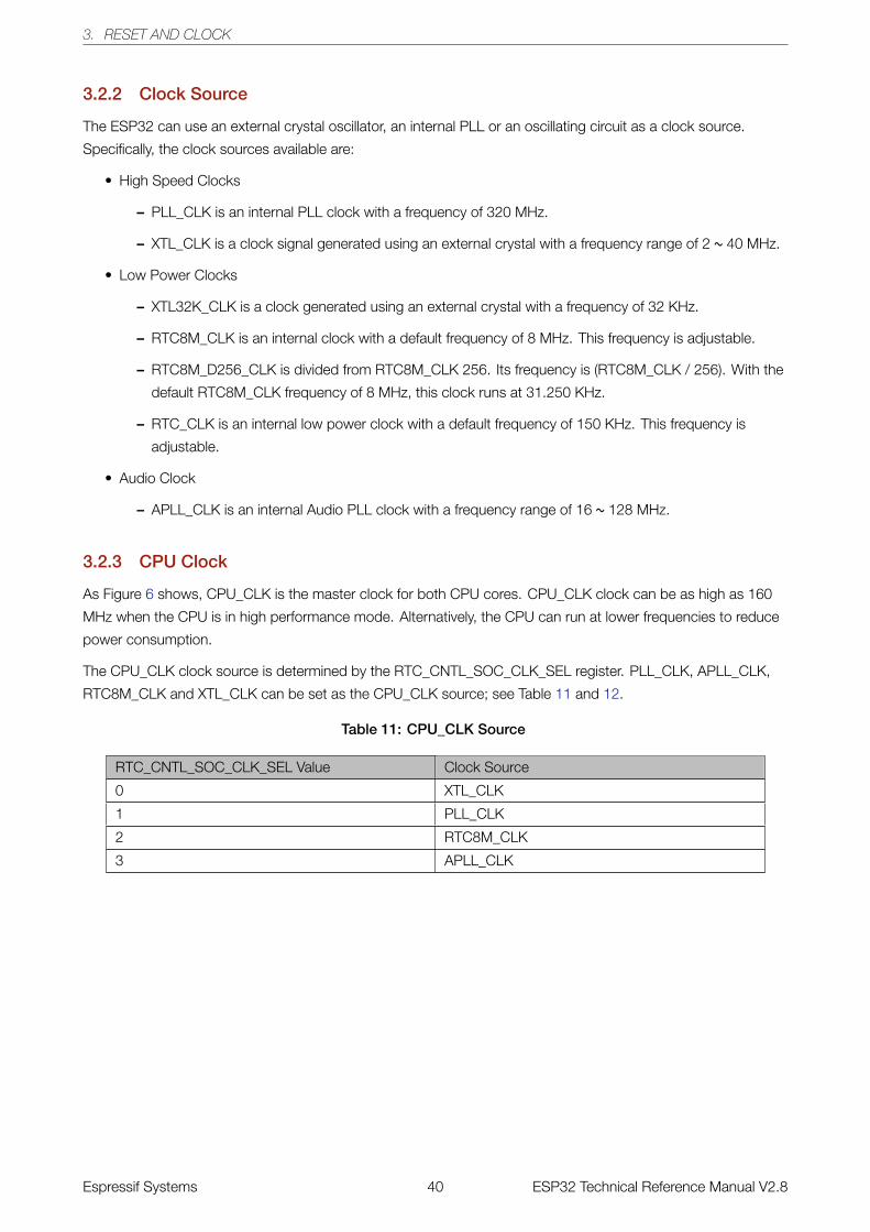
3.2.2 Clock Source 40
3.2.3 CPU Clock 40
3.2.4 Peripheral Clock 41
3.2.4.1 APB_CLK Source 41
3.2.4.2 REF_TICK Source 42
3.2.4.3 LEDC_SCLK Source 42
3.2.4.4 APLL_SCLK Source 42
3.2.4.5 PLL_D2_CLK Source 42
3.2.4.6 Clock Source Considerations 43
3.2.5 Wi-Fi BT Clock 43
3.2.6 RTC Clock 43
3.2.7 Audio PLL 43
4 IO_MUX and GPIO Matrix 45
4.1 Introduction 45
4.2 Peripheral Input via GPIO Matrix 46
4.2.1 Summary 46
4.2.2 Functional Description 46
4.2.3 Simple GPIO Input 47
4.3 Peripheral Output via GPIO Matrix 47
4.3.1 Summary 47
4.3.2 Functional Description 47
4.3.3 Simple GPIO Output 48
4.4 Direct I/O via IO_MUX 48
4.4.1 Summary 49
4.4.2 Functional Description 49
4.5 RTC IO_MUX for Low Power and Analog I/O 49
4.5.1 Summary 49
4.5.2 Functional Description 49
4.6 Light-sleep Mode Pin Functions 50
4.7 Pad Hold Feature 50
4.8 I/O Pad Power Supply 50
4.8.1 VDD_SDIO Power Domain 50
4.9 Peripheral Signal List 51
4.10 IO_MUX Pad List 56
4.11 RTC_MUX Pin List 57
4.12 Register Summary 57
4.13 Registers 61
5 DPort Register 82
5.1 Introduction 82
5.2 Features 82
5.3 Functional Description 82
5.3.1 System and Memory Register 82
5.3.2 Reset and Clock Registers 82
5.3.3 Interrupt Matrix Register 83
5.3.4 DMA Registers 87
5.3.5 PID/MPU/MMU Registers 87
5.3.6 APP_CPU Controller Registers 90
5.3.7 Peripheral Clock Gating and Reset 90
5.4 Register Summary 93
5.5 Registers 99
6 DMA Controller 113

6.1 Overview 113
6.2 Features 113
6.3 Functional Description 113
6.3.1 DMA Engine Architecture 113
6.3.2 Linked List 114
6.4 UART DMA (UDMA) 114
6.5 SPI DMA Interface 115
6.6 I2S DMA Interface 116
7 SPI 118
7.1 Overview 118
7.2 SPI Features 118
7.3 GP-SPI 119
7.3.1 GP-SPI Master Mode 119
7.3.2 GP-SPI Slave Mode 120
7.3.2.1 Communication Format Supported by GP-SPI Slave 120
7.3.2.2 Command Definitions Supported by GP-SPI Slave in Half-duplex Mode 120
7.3.3 GP-SPI Data Buffer 121
7.4 GP-SPI Clock Control 121
7.4.1 GP-SPI Clock Polarity (CPOL) and Clock Phase (CPHA) 122
7.4.2 GP-SPI Timing 122
7.5 Parallel QSPI 123
7.5.1 Communication Format of Parallel QSPI 124
7.6 GP-SPI Interrupt Hardware 124
7.6.1 SPI Interrupts 124
7.6.2 DMA Interrupts 125
7.7 Register Summary 125
7.8 Registers 128
8 SDIO Slave 150
8.1 Overview 150
8.2 Features 150
8.3 Functional Description 150
8.3.1 SDIO Slave Block Diagram 150
8.3.2 Sending and Receiving Data on SDIO Bus 151
8.3.3 Register Access 151
8.3.4 DMA 152
8.3.5 Packet-Sending/-Receiving Procedure 153
8.3.5.1 Sending Packets to SDIO Host 153
8.3.5.2 Receiving Packets from SDIO Host 154
8.3.6 SDIO Bus Timing 155
8.3.7 Interrupt 156
8.3.7.1 Host Interrupt 156
8.3.7.2 Slave Interrupt 156
8.4 Register Summary 157
8.5 SLC Registers 159
8.6 SLC Host Registers 167
8.7 HINF Registers 180
9 SD/MMC Host Controller 181
9.1 Overview 181
9.2 Features 181
9.3 SD/MMC External Interface Signals 181
9.4 Functional Description 182
9.4.1 SD/MMC Host Controller Architecture 182
9.4.1.1 BIU 183
9.4.1.2 CIU 183
9.4.2 Command Path 183
9.4.3 Data Path 184
9.4.3.1 Data Transmit Operation 184
9.4.3.2 Data Receive Operation 185
9.5 Software Restrictions for Proper CIU Operation 185
9.6 RAM for Receiving and Sending Data 186
9.6.1 Transmit RAM Module 186
9.6.2 Receive RAM Module 187
9.7 Descriptor Chain 187
9.8 The Structure of a Linked List 187
9.9 Initialization 189
9.9.1 DMAC Initialization 189
9.9.2 DMAC Transmission Initialization 190
9.9.3 DMAC Reception Initialization 190
9.10 Clock Phase Selection 191
9.11 Interrupt 191
9.12 Register Summary 192
9.13 Registers 193
10 Ethernet MAC 213
10.1 Overview 213
10.2 EMAC_CORE 215
10.2.1 Transmit Operation 215
10.2.1.1 Transmit Flow Control 216
10.2.1.2 Retransmission During a Collision 216
10.2.2 Receive Operation 216
10.2.2.1 Reception Protocol 217
10.2.2.2 Receive Frame Controller 217
10.2.2.3 Receive Flow Control 217
10.2.2.4 Reception of Multiple Frames 218
10.2.2.5 Error Handling 218
10.2.2.6 Receive Status Word 218
10.3 MAC Interrupt Controller 218
10.4 MAC Address Filtering 219
10.4.1 Unicast Destination Address Filtering 219
10.4.2 Multicast Destination Address Filtering 219
10.4.3 Broadcast Address Filtering 219
10.4.4 Unicast Source Address Filtering 219
10.4.5 Inverse Filtering Operation 220
10.4.6 Good Transmitted Frames and Received Frames 221
10.5 EMAC_MTL (MAC Transaction Layer) 222
10.6 PHY Interface 222
10.6.1 MII (Media Independent Interface) 222
10.6.1.1 Interface Signals Between MII and PHY 222
10.6.1.2 MII Clock 223
10.6.2 RMII (Reduced Media-Independent Interface) 224
10.6.2.1 RMII Interface Signal Description 224
10.6.2.2 RMII Clock 225
10.6.3 Station Management Agent (SMA) Interface 225
10.7 Ethernet DMA Features 225
10.8 Linked List Descriptors 226
10.8.1 Transmit Descriptors 226
10.8.2 Receive Descriptors 232
10.9 Register Summary 237
10.10Registers 239
11 I2C Controller 264
11.1 Overview 264
11.2 Features 264
11.3 Functional Description 264
11.3.1 Introduction 264
11.3.2 Architecture 265
11.3.3 I2C Bus Timing 266
11.3.4 I2C cmd Structure 266
11.3.5 I2C Master Writes to Slave 267
11.3.6 I2C Master Reads from Slave 271
11.3.7 Interrupts 273
11.4 Register Summary 274
11.5 Registers 276
12 I2S 287
12.1 Overview 287
12.2 Features 288
12.3 The Clock of I2S Module 289
12.4 I2S Mode 290
12.4.1 Supported Audio Standards 290
12.4.1.1 Philips Standard 290
12.4.1.2 MSB Alignment Standard 290
12.4.1.3 PCM Standard 291
12.4.2 Module Reset 291
12.4.3 FIFO Operation 291
12.4.4 Sending Data 292
12.4.5 Receiving Data 293
12.4.6 I2S Master/Slave Mode 295
12.4.7 I2S PDM 295
12.5 LCD Mode 297
12.5.1 LCD Master Transmitting Mode 297
12.5.2 Camera Slave Receiving Mode 298
12.5.3 ADC/DAC mode 299
12.6 I2S Interrupts 300
12.6.1 FIFO Interrupts 300
12.6.2 DMA Interrupts 300
12.7 Register Summary 301
12.8 Registers 303
13 UART Controllers 320
13.1 Overview 320
13.2 UART Features 320
13.3 Functional Description 320
13.3.1 Introduction 320
13.3.2 UART Architecture 321
13.3.3 UART RAM 322
13.3.4 Baud Rate Detection 322
13.3.5 UART Data Frame 323
13.3.6 Flow Control 324
13.3.6.1 Hardware Flow Control 324
13.3.6.2 Software Flow Control 325
13.3.7 UART DMA 325
13.3.8 UART Interrupts 325
13.3.9 UCHI Interrupts 326
13.4 Register Summary 326
13.5 Registers 330
14 LED_PWM 357
14.1 Introduction 357
14.2 Functional Description 357
14.2.1 Architecture 357
14.2.2 Timers 358
14.2.3 Channels 358
14.2.4 Interrupts 359
14.3 Register Summary 360
14.4 Registers 363
15 Remote Control Peripheral 373
15.1 Introduction 373
15.2 Functional Description 373
15.2.1 RMT Architecture 373
15.2.2 RMT RAM 374
15.2.3 Clock 374
15.2.4 Transmitter 375
15.2.5 Receiver 375
15.2.6 Interrupts 375
15.3 Register Summary 375
15.4 Registers 377
16 MCPWM 382
16.1 Introduction 382
16.2 Features 382
16.3 Submodules 384
16.3.1 Overview 384
16.3.1.1 Prescaler Submodule 384
16.3.1.2 Timer Submodule 384
16.3.1.3 Operator Submodule 385
16.3.1.4 Fault Detection Submodule 387
16.3.1.5 Capture Submodule 387
16.3.2 PWM Timer Submodule 387
16.3.2.1 Configurations of the PWM Timer Submodule 387
16.3.2.2 PWM Timer’s Working Modes and Timing Event Generation 388
16.3.2.3 PWM Timer Shadow Register 392
16.3.2.4 PWM Timer Synchronization and Phase Locking 392
16.3.3 PWM Operator Submodule 392
16.3.3.1 PWM Generator Submodule 393
16.3.3.2 Dead Time Generator Submodule 403
16.3.3.3 PWM Carrier Submodule 407
16.3.3.4 Fault Handler Submodule 409
16.3.4 Capture Submodule 411
16.3.4.1 Introduction 411
16.3.4.2 Capture Timer 411
16.3.4.3 Capture Channel 411
16.4 Register Summary 412
16.5 Registers 414
17 PULSE_CNT 457
17.1 Introduction 457
17.2 Functional Description 457
17.2.1 Architecture 457
17.2.2 Counter Channel Inputs 457
17.2.3 Watchpoints 458
17.2.4 Examples 459
17.2.5 Interrupts 459
17.3 Register Summary 459
17.4 Registers 461
18 64-bit Timers 465
18.1 Introduction 465
18.2 Functional Description 465
18.2.1 16-bit Prescaler 465
18.2.2 64-bit Time-base Counter 465
18.2.3 Alarm Generation 466
18.2.4 MWDT 466
18.2.5 Interrupts 466
18.3 Register Summary 466
18.4 Registers 468
19 Watchdog Timers 475
19.1 Introduction 475
19.2 Features 475
19.3 Functional Description 475
19.3.1 Clock 475
19.3.1.1 Operating Procedure 476
19.3.1.2 Write Protection 476
19.3.1.3 Flash Boot Protection 476
19.3.1.4 Registers 477
20 eFuse Controller 478
20.1 Introduction 478
20.2 Features 478
20.3 Functional Description 478
20.3.1 Structure 478
20.3.1.1 System Parameter efuse_wr_disable 479
20.3.1.2 System Parameter efuse_rd_disable 480
20.3.1.3 System Parameter coding_scheme 480
20.3.1.4 BLK3_part_reserve 481
20.3.2 Programming of System Parameters 481
20.3.3 Software Reading of System Parameters 484
20.3.4 The Use of System Parameters by Hardware Modules 485
20.3.5 Interrupts 485
20.4 Register Summary 486
20.5 Registers 488
21 AES Accelerator 498
21.1 Introduction 498
21.2 Features 498
21.3 Functional Description 498
21.3.1 AES Algorithm Operations 498
21.3.2 Key, Plaintext and Ciphertext 498
21.3.3 Endianness 499
21.3.4 Encryption and Decryption Operations 501
21.3.5 Speed 501
21.4 Register Summary 501
21.5 Registers 503
22 SHA Accelerator 505
22.1 Introduction 505
22.2 Features 505
22.3 Functional Description 505
22.3.1 Padding and Parsing the Message 505
22.3.2 Message Digest 505
22.3.3 Hash Operation 506
22.3.4 Speed 506
22.4 Register Summary 506
22.5 Registers 508
23 RSA Accelerator 513
23.1 Introduction 513
23.2 Features 513
23.3 Functional Description 513
23.3.1 Initialization 513
23.3.2 Large Number Modular Exponentiation 513
23.3.3 Large Number Modular Multiplication 515
23.3.4 Large Number Multiplication 515
23.4 Register Summary 516
23.5 Registers 517
24 Random Number Generator 519
24.1 Introduction 519
24.2 Feature 519
24.3 Functional Description 519
24.4 Register Summary 519
24.5 Register 519
25 Flash Encryption/Decryption 520
25.1 Overview 520
25.2 Features 520
25.3 Functional Description 520
25.3.1 Key Generator 521
25.3.2 Flash Encryption Block 521
25.3.3 Flash Decryption Block 522
25.4 Register Summary 522
25.5 Register 524
26 PID/MPU/MMU 525
26.1 Introduction 525
26.2 Features 525
26.3 Functional Description 525
26.3.1 PID Controller 525
26.3.2 MPU/MMU 526
26.3.2.1 Embedded Memory 526
26.3.2.2 External Memory 532
26.3.2.3 Peripheral 538
27 PID Controller 540
27.1 Overview 540
27.2 Features 540
27.3 Functional Description 540
27.3.1 Interrupt Identification 541
27.3.2 Information Recording 541
27.3.3 Proactive Process Switching 543
27.4 Register Summary 545
27.5 Registers 546
28 On-Chip Sensors and Analog Signal Processing 550
28.1 Introduction 550
28.2 Capacitive Touch Sensor 550
28.2.1 Introduction 550
28.2.2 Features 550
28.2.3 Available GPIOs 551
28.2.4 Functional Description 551
28.2.5 Touch FSM 552
28.3 SAR ADC 553
28.3.1 Introduction 553
28.3.2 Features 554
28.3.3 Outline of Function 554
28.3.4 RTC SAR ADC Controllers 556
28.3.5 DIG SAR ADC Controllers 557
28.4 Low-Noise Amplifier 559
28.4.1 Introduction 559
28.4.2 Features 559
28.4.3 Overview of Function 559
28.5 Hall Sensor 560
28.5.1 Introduction 560
28.5.2 Features 561
28.5.3 Functional Description 561
28.6 Temperature Sensor 561
28.6.1 Introduction 561
28.6.2 Features 562
28.6.3 Functional Description 562
28.7 DAC 562
28.7.1 Introduction 562
28.7.2 Features 562
28.7.3 Structure 563
28.7.4 Cosine Waveform Generator 563
28.7.5 DMA support 564
28.8 Register Summary 565
28.8.1 Sensors 565
28.8.2 Advanced Peripheral Bus 565
28.8.3 RTC I/O 566
28.9 Registers 567
28.9.1 Sensors 567
28.9.2 Advanced Peripheral Bus 578
28.9.3 RTC I/O 581
29 ULP Co-processor 582
29.1 Introduction 582
29.2 Features 582
29.3 Functional Description 583
29.4 Instruction Set 583
29.4.1 ALU - Perform Arithmetic/Logic Operations 584
29.4.1.1 Operations among Registers 584
29.4.1.2 Operations with Immediate Value 585
29.4.1.3 Operations with Stage Count Register 585
29.4.2 ST – Store Data in Memory 586
29.4.3 LD – Load Data from Memory 586
29.4.4 JUMP – Jump to an Absolute Address 587
29.4.5 JUMPR – Jump to a Relative Offset (Conditional upon R0) 587
29.4.6 JUMPS – Jump to a Relative Address (Conditional upon Stage Count Register) 588
29.4.7 HALT – End the Program 588
29.4.8 WAKE – Wake up the Chip 589
29.4.9 Sleep – Set the ULP Timer’s Wake-up Period 589
29.4.10 WAIT – Wait for a Number of Cycles 589
29.4.11 TSENS – Take Measurements with the Temperature Sensor 589
29.4.12 ADC – Take Measurement with ADC 590
29.4.13 I2C_RD/I2C_WR – Read/Write I2C 591
29.4.14 REG_RD – Read from Peripheral Register 591
29.4.15 REG_WR – Write to Peripheral Register 592
29.5 ULP Program Execution 592
29.6 RTC_I2C Controller 594
29.6.1 Configuring RTC_I2C 594
29.6.2 Using RTC_I2C 594
29.6.2.1 I2C_RD - Read a Single Byte 595
29.6.2.2 I2C_WR - Write a Single Byte 595
29.6.2.3 Detecting Error Conditions 596
29.6.2.4 Connecting I2C Signals 596
29.7 Register Summary 597
29.7.1 SENS_ULP Address Space 597
29.7.2 RTC_I2C Address Space 597
29.8 Registers 598
29.8.1 SENS_ULP Address Space 598
29.8.2 RTC_I2C Address Space 600
30 Low-Power Management 607
30.1 Introduction 607
30.2 Features 607
30.3 Functional Description 608
30.3.1 Overview 608
30.3.2 Digital Core Voltage Regulator 608

30.3.3 Low-Power Voltage Regulator 608
30.3.4 Flash Voltage Regulator 609
30.3.5 Brownout Detector 610
30.3.6 RTC Module 610
30.3.7 Low-Power Clocks 612
30.3.8 Power-Gating Implementation 613
30.3.9 Predefined Power Modes 614
30.3.10 Wakeup Source 615
30.3.11 RTC Timer 616
30.3.12 RTC Boot 616
30.4 Register Summary 618
30.5 Registers 620
List of Tables2 Address Mapping 25
3 Embedded Memory Address Mapping 26
4 Module with DMA 28
5 External Memory Address Mapping 29
6 Cache memory mode 29
7 Peripheral Address Mapping 30
8 PRO_CPU, APP_CPU Interrupt Configuration 34
9 CPU Interrupts 36
10 PRO_CPU and APP_CPU Reset Reason Values 38
11 CPU_CLK Source 40
12 CPU_CLK Derivation 41
13 Peripheral Clock Usage 41
14 APB_CLK Derivation 42
15 REF_TICK Derivation 42
16 LEDC_SCLK Derivation 42
17 IO_MUX Light-sleep Pin Function Registers 50
18 GPIO Matrix Peripheral Signals 51
19 IO_MUX Pad Summary 56
20 RTC_MUX Pin Summary 57
25 SPI Signal and Pin Signal Function Mapping 118
26 Clock Polarity and Phase, and Corresponding SPI Register Values for SPI Master 122
27 Clock Polarity and Phase, and Corresponding SPI Register Values for SPI Slave 122
32 SD/MMC Signal Description 182
33 DES0 188
34 DES1 189
35 DES2 189
36 DES3 189
38 Destination Address Filtering 220
39 Source Address Filtering 221
40 Transmit Descriptor 0 (TDES0) 226
41 Transmit Descriptor 1 (TDES1) 230
42 Transmit Descriptor 2 (TDES2) 230
43 Transmit Descriptor 3 (TDES3) 230
44 Transmit Descriptor 6 (TDES6) 230
45 Transmit Descriptor 7 (TDES7) 231
46 Receive Descriptor 0 (RDES0) 232
47 Receive Descriptor 1 (RDES1) 234
48 Receive Descriptor 2 (RDES2) 235
49 Receive Descriptor 3 (RDES3) 235
50 Receive Descriptor 4 (RDES4) 235
51 Receive Descriptor 6 (RDES6) 237
52 Receive Descriptor 7 (RDES7) 237
55 I2S Signal Bus Description 288
56 Register Configuration 292
57 Send Channel Mode 292
58 Modes of Writing Received Data into FIFO and the Corresponding Register Configuration 294
59 The Register Configuration to Which the Four Modes Correspond 294
60 Upsampling Rate Configuration 296
61 Down-sampling Configuration 297
67 Configuration Parameters of the Operator Submodule 386
68 Timing Events Used in PWM Generator 394
69 Timing Events Priority When PWM Timer Increments 394
70 Timing Events Priority when PWM Timer Decrements 395
71 Dead Time Generator Switches Control Registers 404
72 Typical Dead Time Generator Operating Modes 405
77 System Parameter 478
78 BLOCK1/2/3 Encoding 480
79 Program Register 482
80 Timing Configuration 483
81 Software Read Register 484
83 Operation Mode 498
84 AES Text Endianness 499
85 AES-128 Key Endianness 500
86 AES-192 Key Endianness 500
87 AES-256 Key Endianness 500
93 MPU and MMU Structure for Internal Memory 526
94 MPU for RTC FAST Memory 527
95 MPU for RTC SLOW Memory 527
96 Page Mode of MMU for the Remaining 128 KB of Internal SRAM0 and SRAM2 528
97 Page Boundaries for SRAM0 MMU 529
98 Page Boundaries for SRAM2 MMU 529
99 DPORT_DMMU_TABLEn_REG & DPORT_IMMU_TABLEn_REG 530
100 MPU for DMA 531
101 Virtual Address for External Memory 533
102 MMU Entry Numbers for PRO_CPU 533
103 MMU Entry Numbers for APP_CPU 533
104 MMU Entry Numbers for PRO_CPU (Special Mode) 534
105 MMU Entry Numbers for APP_CPU (Special Mode) 534
106 Virtual Address Mode for External SRAM 535
107 Virtual Address for External SRAM ( Normal Mode ) 536
108 Virtual Address for External SRAM ( Low-High Mode ) 536
109 Virtual Address for External SRAM ( Even-Odd Mode ) 536
110 MMU Entry Numbers for External RAM 537
111 MPU for Peripheral 538
112 DPORT_AHBLITE_MPU_TABLE_X_REG 539
113 Interrupt Vector Entry Address 541
114 Configuration of PIDCTRL_LEVEL_REG 541
115 Configuration of PIDCTRL_FROM_n_REG 542
117 ESP32 Capacitive Sensing Touch Pads 551
118 Inputs of SAR ADC module 555
119 ESP32 SAR ADC Controllers 556
120 Fields of the Pattern Table Register 558

121 Fields of Type I DMA Data Format 559
122 Fields of Type II DMA Data Format 559
125 ALU Operations among Registers 584
126 ALU Operations with Immediate Value 585
127 ALU Operations with Stage Count Register 586
128 Input Signals Measured using the ADC Instruction 590
131 RTC Power Domains 613
132 Wake-up Source 616
List of Figures1 System Structure 24
2 System Address Mapping 24
3 Cache Block Diagram 29
4 Interrupt Matrix Structure 33
5 System Reset 38
6 System Clock 39
7 IO_MUX, RTC IO_MUX and GPIO Matrix Overview 45
8 Peripheral Input via IO_MUX, GPIO Matrix 46
9 Output via GPIO Matrix 48
10 ESP32 I/O Pad Power Sources 51
11 DMA Engine Architecture 113
12 Linked List Structure 114
13 Data Transfer in UDMA Mode 115
14 SPI DMA 116
15 SPI Architecture 118
16 SPI Master and Slave Full-duplex Communication 119
17 SPI Data Buffer 121
18 Parallel QSPI 123
19 Communication Format of Parallel QSPI 124
20 SDIO Slave Block Diagram 150
21 SDIO Bus Packet Transmission 151
22 CMD53 Content 151
23 SDIO Slave DMA Linked List Structure 152
24 SDIO Slave Linked List 152
25 Packet Sending Procedure (Initiated by Slave) 153
26 Packet Receiving Procedure (Initiated by Host) 154
27 Loading Receiving Buffer 155
28 Sampling Timing Diagram 155
29 Output Timing Diagram 156
30 SD/MMC Controller Topology 181
31 SD/MMC Controller External Interface Signals 182
32 SDIO Host Block Diagram 182
33 Command Path State Machine 184
34 Data Transmit State Machine 184
35 Data Receive State Machine 185
36 Descriptor Chain 187
37 The Structure of a Linked List 187
38 Clock Phase Selection 191
39 Ethernet MAC Functionality Overview 213
40 Ethernet Block Diagram 215
41 MII Interface 222
42 MII Clock 224
43 RMII Interface 224
44 RMII Clock 225
45 Transmit Descriptor 226
46 Receive Descriptor 232
47 I2C Master Architecture 265
48 I2C Slave Architecture 265
49 I2C Sequence Chart 266
50 Structure of The I2C Command Register 266
51 I2C Master Writes to Slave with 7-bit Address 267
52 I2C Master Writes to Slave with 10-bit Address 269
53 I2C Master Writes to addrM in RAM of Slave with 7-bit Address 269
54 I2C Master Writes to Slave with 7-bit Address in Three Segments 270
55 I2C Master Reads from Slave with 7-bit Address 271
56 I2C Master Reads from Slave with 10-bit Address 271
57 I2C Master Reads N Bytes of Data from addrM in Slave with 7-bit Address 272
58 I2C Master Reads from Slave with 7-bit Address in Three Segments 272
59 I2S System Block Diagram 287
60 I2S Clock 289
61 Philips Standard 290
62 MSB Alignment Standard 290
63 PCM Standard 291
64 Tx FIFO Data Mode 292
65 The First Stage of Receiving Data 293
66 Modes of Writing Received Data into FIFO 294
67 PDM Transmitting Module 295
68 PDM Sends Signal 296
69 PDM Receives Signal 296
70 PDM Receive Module 297
71 LCD Master Transmitting Mode 297
72 LCD Master Transmitting Data Frame, Form 1 298
73 LCD Master Transmitting Data Frame, Form 2 298
74 Camera Slave Receiving Mode 298
75 ADC Interface of I2S0 299
76 DAC Interface of I2S 299
77 Data Input by I2S DAC Interface 299
78 UART Basic Structure 321
79 UART shared RAM 322
80 UART Data Frame Structure 323
81 AT_CMD Character Format 323
82 Hardware Flow Control 324
83 LED_PWM Architecture 357
84 LED_PWM High-speed Channel Diagram 357
85 LED_PWM Divider 358
86 LED PWM Output Signal Diagram 359
87 Output Signal Diagram of Gradient Duty Cycle 359
88 RMT Architecture 373
89 Data Structure 374
90 MCPWM Module Overview 382
91 Prescaler Submodule 384
92 Timer Submodule 384
93 Operator Submodule 385
94 Fault Detection Submodule 387
95 Capture Submodule 387
96 Count-Up Mode Waveform 388
97 Count-Down Mode Waveforms 389
98 Count-Up-Down Mode Waveforms, Count-Down at Synchronization Event 389
99 Count-Up-Down Mode Waveforms, Count-Up at Synchronization Event 389
100 UTEP and UTEZ Generation in Count-Up Mode 390
101 DTEP and DTEZ Generation in Count-Down Mode 391
102 DTEP and UTEZ Generation in Count-Up-Down Mode 391
103 Submodules Inside the PWM Operator 393
104 Symmetrical Waveform in Count-Up-Down Mode 396
105 Count-Up, Single Edge Asymmetric Waveform, with Independent Modulation on PWMxA and PWMxB
— Active High 397
106 Count-Up, Pulse Placement Asymmetric Waveform with Independent Modulation on PWMxA 398
107 Count-Up-Down, Dual Edge Symmetric Waveform, with Independent Modulation on PWMxA and
PWMxB — Active High 399
108 Count-Up-Down, Dual Edge Symmetric Waveform, with Independent Modulation on PWMxA and
PWMxB — Complementary 400
109 Example of an NCI Software-Force Event on PWMxA 401
110 Example of a CNTU Software-Force Event on PWMxB 402
111 Options for Setting up the Dead Time Generator Submodule 404
112 Active High Complementary (AHC) Dead Time Waveforms 405
113 Active Low Complementary (ALC) Dead Time Waveforms 406
114 Active High (AH) Dead Time Waveforms 406
115 Active Low (AL) Dead Time Waveforms 406
116 Example of Waveforms Showing PWM Carrier Action 408
117 Example of the First Pulse and the Subsequent Sustaining Pulses of the PWM Carrier Submodule 409
118 Possible Duty Cycle Settings for Sustaining Pulses in the PWM Carrier Submodule 409
119 PULSE_CNT Architecture 457
120 PULSE_CNT Upcounting Diagram 459
121 PULSE_CNT Downcounting Diagram 459
122 Flash Encryption/Decryption Module Architecture 520
123 MMU Access Example 528
124 Interrupt Nesting 543
125 Touch Sensor 550
126 Touch Sensor Structure 551
127 Touch Sensor Operating Flow 552
128 Touch FSM Structure 553
129 SAR ADC Depiction 554
130 SAR ADC Outline of Function 555
131 RTC SAR ADC Outline of Function 557
132 Diagram of DIG SAR ADC Controllers 558
133 Structure of Low-Noise Amplifier 559
134 Low-Noise Amplifier – Sequence of Operation 560
135 Hall Sensor 561
136 Temperature Sensor 562
137 Diagram of DAC Function 563
138 Cosine Waveform (CW) Generator 564
139 ULP Co-processor Diagram 582
140 The ULP Co-processor Instruction Format 583
141 Instruction Type — ALU for Operations among Registers 584
142 Instruction Type — ALU for Operations with Immediate Value 585
143 Instruction Type — ALU for Operations with Stage Count Register 585
144 Instruction Type — ST 586
145 Instruction Type — LD 586
146 Instruction Type — JUMP 587
147 Instruction Type — JUMPR 587
148 Instruction Type — JUMP 588
149 Instruction Type — HALT 588
150 Instruction Type — WAKE 589
151 Instruction Type — SLEEP 589
152 Instruction Type — WAIT 589
153 Instruction Type — TSENS 589
154 Instruction Type — ADC 590
155 Instruction Type — I2C 591
156 Instruction Type — REG_RD 591
157 Instruction Type — REG_WR 592
158 Control of ULP Program Execution 593
159 Sample of a ULP Operation Sequence 594
160 I2C Read Operation 595
161 I2C Write Operation 596
162 ESP32 Power Control 607
163 Digital Core Voltage Regulator 608
164 Low-Power Voltage Regulator 609
165 Flash Voltage Regulator 610
166 Brownout Detector 610
167 RTC Structure 611
168 RTC Low-Power Clocks 612
169 Digital Low-Power Clocks 612
170 RTC States 613
171 Power Modes 615
172 ESP32 Boot Flow 617
1. SYSTEM AND MEMORY
1. System and Memory
1.1 Introduction
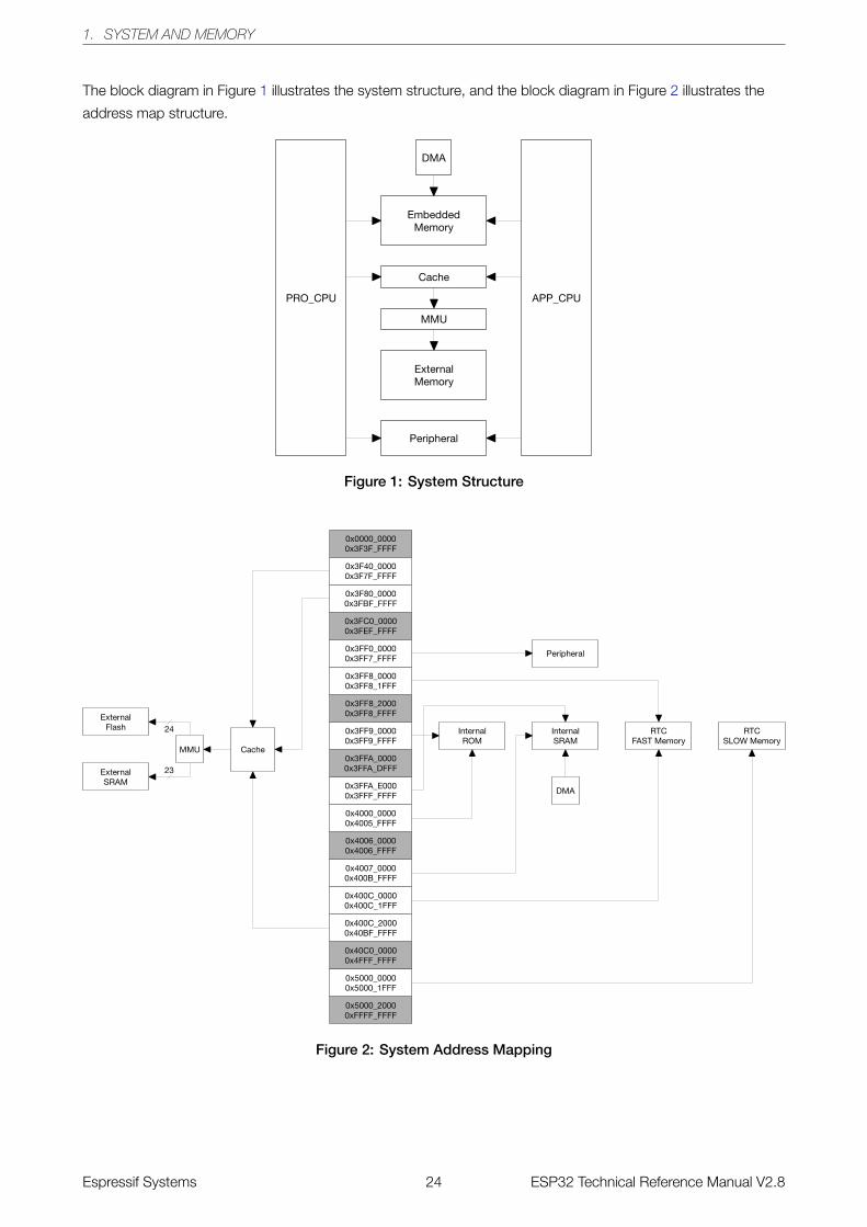
The ESP32 is a dual-core system with two Harvard Architecture Xtensa LX6 CPUs. All embedded memory,
external memory and peripherals are located on the data bus and/or the instruction bus of these CPUs.
With some minor exceptions (see below), the address mapping of two CPUs is symmetric, meaning that they use
the same addresses to access the same memory. Multiple peripherals in the system can access embedded
memory via DMA.
The two CPUs are named “PRO_CPU” and “APP_CPU” (for “protocol” and “application”), however, for most
purposes the two CPUs are interchangeable.
1.2 Features
• Address Space
– Symmetric address mapping
– 4 GB (32-bit) address space for both data bus and instruction bus
– 1296 KB embedded memory address space
– 19704 KB external memory address space
– 512 KB peripheral address space
– Some embedded and external memory regions can be accessed by either data bus or instruction bus
– 328 KB DMA address space
• Embedded Memory
– 448 KB Internal ROM
– 520 KB Internal SRAM
– 8 KB RTC FAST Memory
– 8 KB RTC SLOW Memory
• External Memory
Off-chip SPI memory can be mapped into the available address space as external memory. Parts of the
embedded memory can be used as transparent cache for this external memory.
– Supports up to 16 MB off-Chip SPI Flash.
– Supports up to 8 MB off-Chip SPI SRAM.
• Peripherals
– 41 peripherals
• DMA
– 13 modules are capable of DMA operation
Espressif Systems 23 ESP32 Technical Reference Manual V2.8
1. SYSTEM AND MEMORY
The block diagram in Figure 1 illustrates the system structure, and the block diagram in Figure 2 illustrates the
address map structure.
Figure 1: System Structure
Figure 2: System Address Mapping
Espressif Systems 24 ESP32 Technical Reference Manual V2.8
1. SYSTEM AND MEMORY
1.3 Functional Description
1.3.1 Address Mapping
Each of the two Harvard Architecture Xtensa LX6 CPUs has 4 GB (32-bit) address space. Address spaces are
symmetric between the two CPUs.
Addresses below 0x4000_0000 are serviced using the data bus. Addresses in the range 0x4000_0000 ~0x4FFF_FFFF are serviced using the instruction bus. Finally, addresses over and including 0x5000_0000 are
shared by the data and instruction bus.
The data bus and instruction bus are both little-endian: for example, byte addresses 0x0, 0x1, 0x2, 0x3 access
the least significant, second least significant, second most significant, and the most significant bytes of the 32-bit
word stored at the 0x0 address, respectively. The CPU can access data bus addresses via aligned or non-aligned
byte, half-word and word read-and-write operations. The CPU can read and write data through the instruction
bus, but only in a word aligned manner; non-word-aligned access will cause a CPU exception.
Each CPU can directly access embedded memory through both the data bus and the instruction bus, external
memory which is mapped into the address space (via transparent caching & MMU), and peripherals. Table 2
illustrates address ranges that can be accessed by each CPU’s data bus and instruction bus.
Some embedded memories and some external memories can be accessed via the data bus or the instruction
bus. In these cases, the same memory is available to either of the CPUs at two address ranges.
Table 2: Address Mapping
Boundary AddressBus Type
Low Address High AddressSize Target
0x0000_0000 0x3F3F_FFFF Reserved
Data 0x3F40_0000 0x3F7F_FFFF 4 MB External Memory
Data 0x3F80_0000 0x3FBF_FFFF 4 MB External Memory
0x3FC0_0000 0x3FEF_FFFF 3 MB Reserved
Data 0x3FF0_0000 0x3FF7_FFFF 512 KB Peripheral
Data 0x3FF8_0000 0x3FFF_FFFF 512 KB Embedded Memory
Instruction 0x4000_0000 0x400C_1FFF 776 KB Embedded Memory
Instruction 0x400C_2000 0x40BF_FFFF 11512 KB External Memory
0x40C0_0000 0x4FFF_FFFF 244 MB Reserved
Data Instruction 0x5000_0000 0x5000_1FFF 8 KB Embedded Memory
0x5000_2000 0xFFFF_FFFF Reserved
1.3.2 Embedded Memory
The Embedded Memory consists of four segments: internal ROM (448 KB), internal SRAM (520 KB), RTC FAST
memory (8 KB) and RTC SLOW memory (8 KB).
The 448 KB internal ROM is divided into two parts: Internal ROM 0 (384 KB) and Internal ROM 1 (64 KB). The
520 KB internal SRAM is divided into three parts: Internal SRAM 0 (192 KB), Internal SRAM 1 (128 KB), and
Internal SRAM 2 (200 KB). RTC FAST Memory and RTC SLOW Memory are both implemented as SRAM.
Table 3 lists all embedded memories and their address ranges on the data and instruction buses.
Espressif Systems 25 ESP32 Technical Reference Manual V2.8
1. SYSTEM AND MEMORY
Table 3: Embedded Memory Address Mapping
Boundary AddressBus Type
Low Address High AddressSize Target Comment
Data 0x3FF8_0000 0x3FF8_1FFF 8 KB RTC FAST Memory PRO_CPU Only
0x3FF8_2000 0x3FF8_FFFF 56 KB Reserved -
Data 0x3FF9_0000 0x3FF9_FFFF 64 KB Internal ROM 1 -
0x3FFA_0000 0x3FFA_DFFF 56 KB Reserved -
Data 0x3FFA_E000 0x3FFD_FFFF 200 KB Internal SRAM 2 DMA
Data 0x3FFE_0000 0x3FFF_FFFF 128 KB Internal SRAM 1 DMA
Boundary AddressBus Type
Low Address High AddressSize Target Comment
Instruction 0x4000_0000 0x4000_7FFF 32 KB Internal ROM 0 Remap
Instruction 0x4000_8000 0x4005_FFFF 352 KB Internal ROM 0 -
0x4006_0000 0x4006_FFFF 64 KB Reserved -
Instruction 0x4007_0000 0x4007_FFFF 64 KB Internal SRAM 0 Cache
Instruction 0x4008_0000 0x4009_FFFF 128 KB Internal SRAM 0 -
Instruction 0x400A_0000 0x400A_FFFF 64 KB Internal SRAM 1 -
Instruction 0x400B_0000 0x400B_7FFF 32 KB Internal SRAM 1 Remap
Instruction 0x400B_8000 0x400B_FFFF 32 KB Internal SRAM 1 -
Instruction 0x400C_0000 0x400C_1FFF 8 KB RTC FAST Memory PRO_CPU Only
Boundary AddressBus Type
Low Address High AddressSize Target Comment
Data Instruc-
tion0x5000_0000 0x5000_1FFF 8 KB RTC SLOW Memory -
1.3.2.1 Internal ROM 0
The capacity of Internal ROM 0 is 384 KB. It is accessible by both CPUs through the address range
0x4000_0000 ~ 0x4005_FFFF, which is on the instruction bus.
The address range of the first 32 KB of the ROM 0 (0x4000_0000 ~ 0x4000_7FFF) can be remapped in order to
access a part of Internal SRAM 1 that normally resides in a memory range of 0x400B_0000 ~ 0x400B_7FFF.
While remapping, the 32 KB SRAM cannot be accessed by an address range of 0x400B_0000 ~ 0x400B_7FFF
any more, but it can still be accessible through the data bus (0x3FFE_8000 ~ 0x3FFE_FFFF). This can be done
on a per-CPU basis: setting bit 0 of register DPORT_PRO_BOOT_REMAP_CTRL_REG or
DPORT_APP_BOOT_REMAP_CTRL_REG will remap SRAM for the PRO_CPU and APP_CPU,
respectively.
1.3.2.2 Internal ROM 1
The capacity of Internal ROM 1 is 64 KB. It can be read by either CPU at an address range 0x3FF9_0000 ~0x3FF9_FFFF of the data bus.
Espressif Systems 26 ESP32 Technical Reference Manual V2.8
1. SYSTEM AND MEMORY
1.3.2.3 Internal SRAM 0
The capacity of Internal SRAM 0 is 192 KB. Hardware can be configured to use the first 64 KB to cache external
memory access. When not used as cache, the first 64 KB can be read and written by either CPU at addresses
0x4007_0000 ~ 0x4007_FFFF of the instruction bus. The remaining 128 KB can always be read and written by
either CPU at addresses 0x4008_0000 ~ 0x4009_FFFF of instruction bus.
1.3.2.4 Internal SRAM 1
The capacity of Internal SRAM 1 is 128 KB. Either CPU can read and write this memory at addresses
0x3FFE_0000 ~ 0x3FFF_FFFF of the data bus, and also at addresses 0x400A_0000 ~ 0x400B_FFFF of the
instruction bus.
The address range accessed via the instruction bus is in reverse order (word-wise) compared to access via the
data bus. That is to say, address
0x3FFE_0000 and 0x400B_FFFC access the same word
0x3FFE_0004 and 0x400B_FFF8 access the same word
0x3FFE_0008 and 0x400B_FFF4 access the same word
……
0x3FFF_FFF4 and 0x400A_0008 access the same word
0x3FFF_FFF8 and 0x400A_0004 access the same word
0x3FFF_FFFC and 0x400A_0000 access the same word
The data bus and instruction bus of the CPU are still both little-endian, so the byte order of individual words is not
reversed between address spaces. For example, address
0x3FFE_0000 accesses the least significant byte in the word accessed by 0x400B_FFFC.
0x3FFE_0001 accesses the second least significant byte in the word accessed by 0x400B_FFFC.
0x3FFE_0002 accesses the second most significant byte in the word accessed by 0x400B_FFFC.
0x3FFE_0003 accesses the most significant byte in the word accessed by 0x400B_FFFC.
0x3FFE_0004 accesses the least significant byte in the word accessed by 0x400B_FFF8.
0x3FFE_0005 accesses the second least significant byte in the word accessed by 0x400B_FFF8.
0x3FFE_0006 accesses the second most significant byte in the word accessed by 0x400B_FFF8.
0x3FFE_0007 accesses the most significant byte in the word accessed by 0x400B_FFF8.
……
0x3FFF_FFF8 accesses the least significant byte in the word accessed by 0x400A_0004.
0x3FFF_FFF9 accesses the second least significant byte in the word accessed by 0x400A_0004.
0x3FFF_FFFA accesses the second most significant byte in the word accessed by 0x400A_0004.
0x3FFF_FFFB accesses the most significant byte in the word accessed by 0x400A_0004.
0x3FFF_FFFC accesses the least significant byte in the word accessed by 0x400A_0000.
0x3FFF_FFFD accesses the second most significant byte in the word accessed by 0x400A_0000.
0x3FFF_FFFE accesses the second most significant byte in the word accessed by 0x400A_0000.
0x3FFF_FFFF accesses the most significant byte in the word accessed by 0x400A_0000.
Part of this memory can be remapped onto the ROM 0 address space. See Internal Rom 0 for more
information.
Espressif Systems 27 ESP32 Technical Reference Manual V2.8
1. SYSTEM AND MEMORY
1.3.2.5 Internal SRAM 2
The capacity of Internal SRAM 2 is 200 KB. It can be read and written by either CPU at addresses 0x3FFA_E000
~ 0x3FFD_FFFF on the data bus.
1.3.2.6 DMA
DMA uses the same addressing as the CPU data bus to read and write Internal SRAM 1 and Internal SRAM 2.
This means DMA uses an address range of 0x3FFE_0000 ~ 0x3FFF_FFFF to read and write Internal SRAM 1 and
an address range of 0x3FFA_E000 ~ 0x3FFD_FFFF to read and write Internal SRAM 2.
In the ESP32, 13 peripherals are equipped with DMA. Table 4 lists these peripherals.
Table 4: Module with DMA
UART0 UART1 UART2
SPI1 SPI2 SPI3
I2S0 I2S1
SDIO Slave SDMMC
EMAC
BT WIFI
1.3.2.7 RTC FAST Memory
RTC FAST Memory is 8 KB of SRAM. It can be read and written by PRO_CPU only at an address range of
0x3FF8_0000 ~ 0x3FF8_1FFF on the data bus or at an address range of 0x400C_0000 ~ 0x400C_1FFF on the
instruction bus. Unlike most other memory regions, RTC FAST memory cannot be accessed by the
APP_CPU.
The two address ranges of PRO_CPU access RTC FAST Memory in the same order, so, for example, addresses
0x3FF8_0000 and 0x400C_0000 access the same word. On the APP_CPU, these address ranges do not
provide access to RTC FAST Memory or any other memory location.
1.3.2.8 RTC SLOW Memory
RTC SLOW Memory is 8 KB of SRAM which can be read and written by either CPU at an address range of
0x5000_0000 ~ 0x5000_1FFF. This address range is shared by both the data bus and the instruction bus.
1.3.3 External Memory
The ESP32 can access external SPI flash and SPI SRAM as external memory. Table 5 provides a list of external
memories that can be accessed by either CPU at a range of addresses on the data and instruction buses. When
a CPU accesses external memory through the Cache and MMU, the cache will map the CPU’s address to an
external physical memory address (in the external memory’s address space), according to the MMU settings. Due
to this address mapping, the ESP32 can address up to 16 MB External Flash and 8 MB External SRAM.
Espressif Systems 28 ESP32 Technical Reference Manual V2.8
1. SYSTEM AND MEMORY
Table 5: External Memory Address Mapping
Boundary AddressBus Type
Low Address High AddressSize Target Comment
Data 0x3F40_0000 0x3F7F_FFFF 4 MB External Flash Read
Data 0x3F80_0000 0x3FBF_FFFF 4 MB External SRAM Read and Write
Boundary AddressBus Type
Low Address High AddressSize Target Comment
Instruction 0x400C_2000 0x40BF_FFFF 11512 KB External Flash Read
1.3.4 Cache
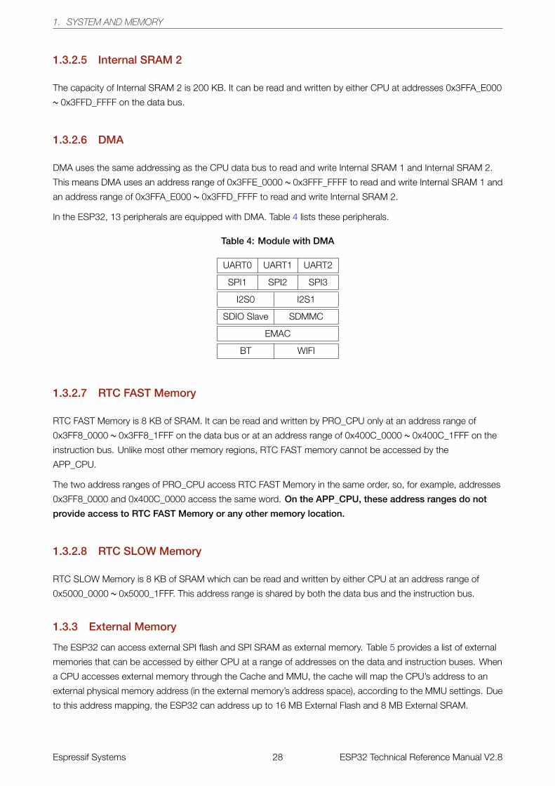
As shown in Figure 3, each of the two CPUs in ESP32 has 32 KB of cache for accessing external storage. PRO
CPU uses bit PRO_CACHE_ENABLE in register DPORT_PRO_CAHCE_CTRL_REG to enable the Cache, while
APP CPU uses bit APP_CACHE_ENABLE in register DPORT_APP_CAHCE_CTRL_REG to enable the same
function.
Figure 3: Cache Block Diagram
ESP32 uses a two-way set-associative cache. When the Cache function is to be used either by PRO CPU or
APP CPU, bit CACHE_MUX_MODE[1:0] in register DPORT_CACHE_MUX_MODE_REG can be set to select
POOL0 or POOL1 in the Internal SRAM0 as the cache memory. When both PRO CPU and APP CPU use the
Cache function, POOL0 and POOL1 in the Internal SRAM0 will be used simultaneously as the cache memory,
while they can also be used by the instruction bus. This is depicted in table 6 below.
Table 6: Cache memory mode
CACHE_MUX_MODE POOL0 POOL1
0 PRO CPU APP CPU
1 PRO CPU/APP CPU -
2 - PRO CPU/APP CPU
3 APP CPU PRO CPU
Espressif Systems 29 ESP32 Technical Reference Manual V2.8
1. SYSTEM AND MEMORY
As described in table 6, when bit CACHE_MUX_MODE is set to 1 or 2, PRO CPU and APP CPU cannot enable
the Cache function at the same time. When the Cache function is enabled, POOL0 or POOL1 can only be used
as the cache memory, and cannot be used by the instruction bus as well.
ESP32 Cache supports the Flush function. It is worth noting that when the Flush function is used, the data
written in the cache will be disposed rather than being rewritten into the External SRAM. To enable the Flush
function, first clear bit x_CACHE_FLUSH_ENA in register DPORT_x_CACHE_CTRL_REG, then set this bit to 1.
Afterwards, the system hardware will set bit x_CACHE_FLUSH_DONE to 1, where x can be ”PRO” or ”APP”,
indicating that the cache flush operation has been completed.
For more information about the address mapping of ESP32 Cache, please refer to Embedded Memory and
External Memory.
1.3.5 Peripherals
The ESP32 has 41 peripherals. Table 7 specifically describes the peripherals and their respective address
ranges. Nearly all peripheral modules can be accessed by either CPU at the same address with just a single
exception; this being the PID Controller.
Table 7: Peripheral Address Mapping
Boundary AddressBus Type
Low Address High AddressSize Target Comment
Data 0x3FF0_0000 0x3FF0_0FFF 4 KB DPort Register
Data 0x3FF0_1000 0x3FF0_1FFF 4 KB AES Accelerator
Data 0x3FF0_2000 0x3FF0_2FFF 4 KB RSA Accelerator
Data 0x3FF0_3000 0x3FF0_3FFF 4 KB SHA Accelerator
Data 0x3FF0_4000 0x3FF0_4FFF 4 KB Secure Boot
0x3FF0_5000 0x3FF0_FFFF 44 KB Reserved
Data 0x3FF1_0000 0x3FF1_3FFF 16 KB Cache MMU Table
0x3FF1_4000 0x3FF1_EFFF 44 KB Reserved
Data 0x3FF1_F000 0x3FF1_FFFF 4 KB PID Controller Per-CPU peripheral
0x3FF2_0000 0x3FF3_FFFF 128 KB Reserved
Data 0x3FF4_0000 0x3FF4_0FFF 4 KB UART0
0x3FF4_1000 0x3FF4_1FFF 4 KB Reserved
Data 0x3FF4_2000 0x3FF4_2FFF 4 KB SPI1
Data 0x3FF4_3000 0x3FF4_3FFF 4 KB SPI0
Data 0x3FF4_4000 0x3FF4_4FFF 4 KB GPIO
0x3FF4_5000 0x3FF4_7FFF 12 KB Reserved
Data 0x3FF4_8000 0x3FF4_8FFF 4 KB RTC
Data 0x3FF4_9000 0x3FF4_9FFF 4 KB IO MUX
0x3FF4_A000 0x3FF4_AFFF 4 KB Reserved
Data 0x3FF4_B000 0x3FF4_BFFF 4 KB SDIO Slave One of three parts
Data 0x3FF4_C000 0x3FF4_CFFF 4 KB UDMA1
0x3FF4_D000 0x3FF4_EFFF 8 KB Reserved
Data 0x3FF4_F000 0x3FF4_FFFF 4 KB I2S0
Data 0x3FF5_0000 0x3FF5_0FFF 4 KB UART1
0x3FF5_1000 0x3FF5_2FFF 8 KB Reserved
Espressif Systems 30 ESP32 Technical Reference Manual V2.8
1. SYSTEM AND MEMORY
Boundary AddressBus Type
Low Address High AddressSize Target Comment
Data 0x3FF5_3000 0x3FF5_3FFF 4 KB I2C0
Data 0x3FF5_4000 0x3FF5_4FFF 4 KB UDMA0
Data 0x3FF5_5000 0x3FF5_5FFF 4 KB SDIO Slave One of three parts
Data 0x3FF5_6000 0x3FF5_6FFF 4 KB RMT
Data 0x3FF5_7000 0x3FF5_7FFF 4 KB PCNT
Data 0x3FF5_8000 0x3FF5_8FFF 4 KB SDIO Slave One of three parts
Data 0x3FF5_9000 0x3FF5_9FFF 4 KB LED PWM
Data 0x3FF5_A000 0x3FF5_AFFF 4 KB Efuse Controller
Data 0x3FF5_B000 0x3FF5_BFFF 4 KB Flash Encryption
0x3FF5_C000 0x3FF5_DFFF 8 KB Reserved
Data 0x3FF5_E000 0x3FF5_EFFF 4 KB PWM0
Data 0x3FF5_F000 0x3FF5_FFFF 4 KB TIMG0
Data 0x3FF6_0000 0x3FF6_0FFF 4 KB TIMG1
0x3FF6_1000 0x3FF6_3FFF 12 KB Reserved
Data 0x3FF6_4000 0x3FF6_4FFF 4 KB SPI2
Data 0x3FF6_5000 0x3FF6_5FFF 4 KB SPI3
Data 0x3FF6_6000 0x3FF6_6FFF 4 KB SYSCON
Data 0x3FF6_7000 0x3FF6_7FFF 4 KB I2C1
Data 0x3FF6_8000 0x3FF6_8FFF 4 KB SDMMC
Data 0x3FF6_9000 0x3FF6_AFFF 8 KB EMAC
0x3FF6_B000 0x3FF6_BFFF 4 KB Reserved
Data 0x3FF6_C000 0x3FF6_CFFF 4 KB PWM1
Data 0x3FF6_D000 0x3FF6_DFFF 4 KB I2S1
Data 0x3FF6_E000 0x3FF6_EFFF 4 KB UART2
Data 0x3FF6_F000 0x3FF6_FFFF 4 KB PWM2
Data 0x3FF7_0000 0x3FF7_0FFF 4 KB PWM3
0x3FF7_1000 0x3FF7_4FFF 16 KB Reserved
Data 0x3FF7_5000 0x3FF7_5FFF 4 KB RNG
0x3FF7_6000 0x3FF7_FFFF 40 KB Reserved
1.3.5.1 Asymmetric PID Controller Peripheral
There are two PID Controllers in the system. They serve the PRO_CPU and the APP_CPU, respectively. The
PRO_CPU and the APP_CPU can only access their own PID Controller and not that of their counterpart.
Each CPU uses the same memory range 0x3FF1_F000 ~ 3FF1_FFFF to access its own PID Controller.
1.3.5.2 Non-Contiguous Peripheral Memory Ranges
The SDIO Slave peripheral consists of three parts and the two CPUs use non-contiguous addresses to access
these. The three parts are accessed at the address ranges 0x3FF4_B000 ~ 3FF4_BFFF, 0x3FF5_5000 ~3FF5_5FFF and 0x3FF5_8000 ~ 3FF5_8FFF of each CPU’s data bus. Similarly to other peripherals, access to
this peripheral is identical for both CPUs.
Espressif Systems 31 ESP32 Technical Reference Manual V2.8
1. SYSTEM AND MEMORY
1.3.5.3 Memory Speed
The ROM as well as the SRAM are both clocked from CPU_CLK and can be accessed by the CPU in a single
cycle. The RTC FAST memory is clocked from the APB_CLOCK and the RTC SLOW memory from the
FAST_CLOCK, so access to these memories may be slower. DMA uses the APB_CLK to access memory.
Internally, the SRAM is organized in 32K-sized banks. Each CPU and DMA channel can simultaneously access
the SRAM at full speed, provided they access addresses in different memory banks.
Espressif Systems 32 ESP32 Technical Reference Manual V2.8
2. INTERRUPT MATRIX
2. Interrupt Matrix
2.1 Introduction
The Interrupt Matrix embedded in the ESP32 independently allocates peripheral interrupt sources to the two
CPUs’ peripheral interrupts. This configuration is made to be highly flexible in order to meet many different needs.
2.2 Features
• Accepts 71 peripheral interrupt sources as input.
• Generates 26 peripheral interrupt sources per CPU as output (52 total).
• CPU NMI Interrupt Mask.
• Queries current interrupt status of peripheral interrupt sources.
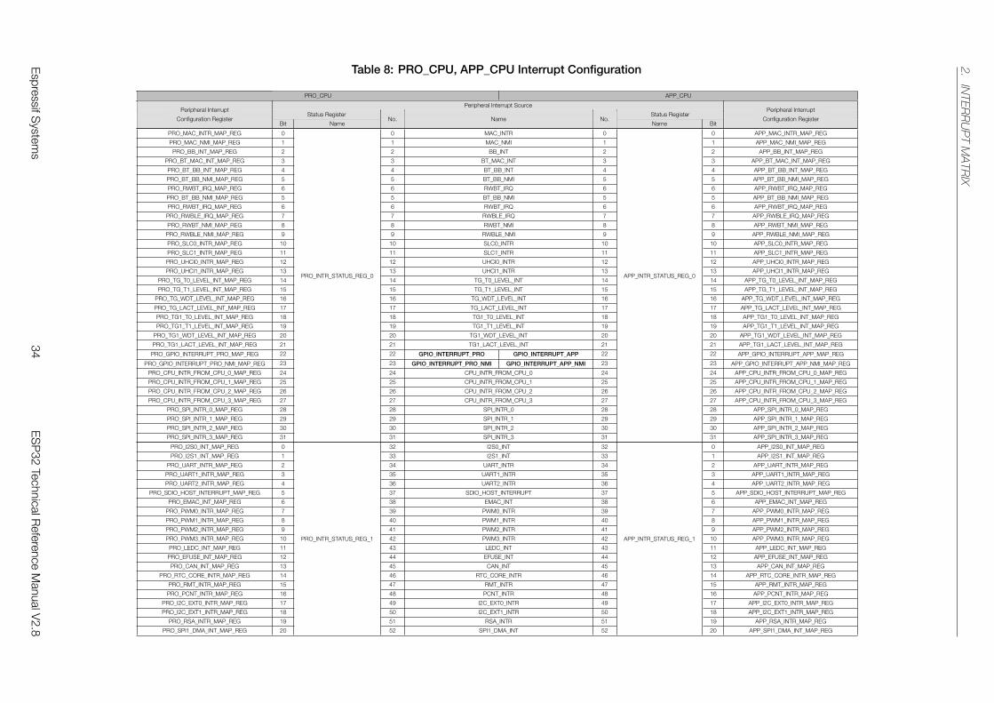
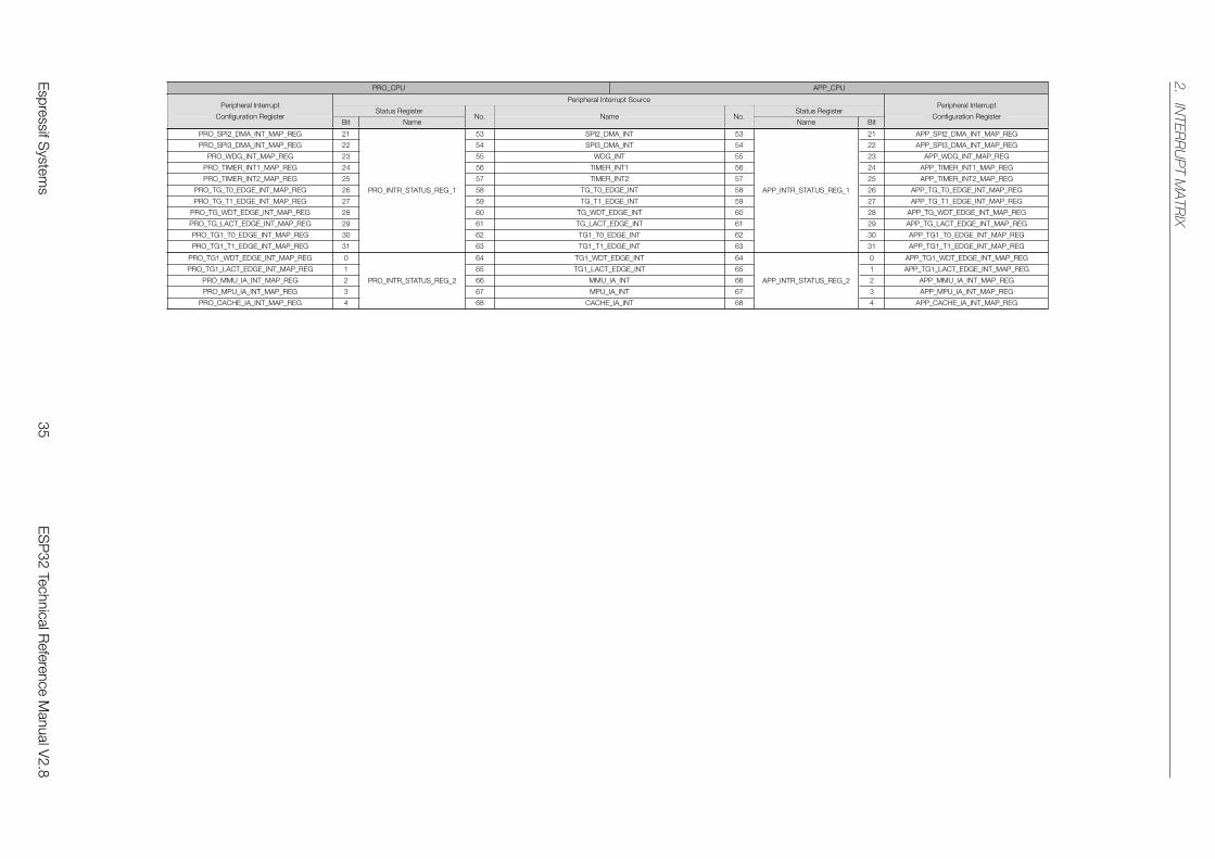
The structure of the Interrupt Matrix is shown in Figure 4.
Figure 4: Interrupt Matrix Structure
2.3 Functional Description
2.3.1 Peripheral Interrupt Source
ESP32 has 71 peripheral interrupt sources in total. All peripheral interrupt sources are listed in table 8. 67 of 71
ESP32 peripheral interrupt sources can be allocated to either CPU.
The four remaining peripheral interrupt sources are CPU-specific, two per CPU. GPIO_INTERRUPT_PRO and
GPIO_INTERRUPT_PRO_NMI can only be allocated to PRO_CPU. GPIO_INTERRUPT_APP and
GPIO_INTERRUPT_APP_NMI can only be allocated to APP_CPU. As a result, PRO_CPU and APP_CPU each
have 69 peripheral interrupt sources.
Espressif Systems 33 ESP32 Technical Reference Manual V2.8
2.INTER
RUPTMATR
IX
Table 8: PRO_CPU, APP_CPU Interrupt Configuration
PRO_CPU APP_CPU
Peripheral Interrupt Source
Status Register Status RegisterPeripheral Interrupt
Configuration RegisterBit Name
No. Name No.Name Bit
Peripheral Interrupt
Configuration Register
PRO_MAC_INTR_MAP_REG 0
PRO_INTR_STATUS_REG_0
0 MAC_INTR 0
APP_INTR_STATUS_REG_0
0 APP_MAC_INTR_MAP_REG
PRO_MAC_NMI_MAP_REG 1 1 MAC_NMI 1 1 APP_MAC_NMI_MAP_REG
PRO_BB_INT_MAP_REG 2 2 BB_INT 2 2 APP_BB_INT_MAP_REG
PRO_BT_MAC_INT_MAP_REG 3 3 BT_MAC_INT 3 3 APP_BT_MAC_INT_MAP_REG
PRO_BT_BB_INT_MAP_REG 4 4 BT_BB_INT 4 4 APP_BT_BB_INT_MAP_REG
PRO_BT_BB_NMI_MAP_REG 5 5 BT_BB_NMI 5 5 APP_BT_BB_NMI_MAP_REG
PRO_RWBT_IRQ_MAP_REG 6 6 RWBT_IRQ 6 6 APP_RWBT_IRQ_MAP_REG
PRO_BT_BB_NMI_MAP_REG 5 5 BT_BB_NMI 5 5 APP_BT_BB_NMI_MAP_REG
PRO_RWBT_IRQ_MAP_REG 6 6 RWBT_IRQ 6 6 APP_RWBT_IRQ_MAP_REG
PRO_RWBLE_IRQ_MAP_REG 7 7 RWBLE_IRQ 7 7 APP_RWBLE_IRQ_MAP_REG
PRO_RWBT_NMI_MAP_REG 8 8 RWBT_NMI 8 8 APP_RWBT_NMI_MAP_REG
PRO_RWBLE_NMI_MAP_REG 9 9 RWBLE_NMI 9 9 APP_RWBLE_NMI_MAP_REG
PRO_SLC0_INTR_MAP_REG 10 10 SLC0_INTR 10 10 APP_SLC0_INTR_MAP_REG
PRO_SLC1_INTR_MAP_REG 11 11 SLC1_INTR 11 11 APP_SLC1_INTR_MAP_REG
PRO_UHCI0_INTR_MAP_REG 12 12 UHCI0_INTR 12 12 APP_UHCI0_INTR_MAP_REG
PRO_UHCI1_INTR_MAP_REG 13 13 UHCI1_INTR 13 13 APP_UHCI1_INTR_MAP_REG
PRO_TG_T0_LEVEL_INT_MAP_REG 14 14 TG_T0_LEVEL_INT 14 14 APP_TG_T0_LEVEL_INT_MAP_REG
PRO_TG_T1_LEVEL_INT_MAP_REG 15 15 TG_T1_LEVEL_INT 15 15 APP_TG_T1_LEVEL_INT_MAP_REG
PRO_TG_WDT_LEVEL_INT_MAP_REG 16 16 TG_WDT_LEVEL_INT 16 16 APP_TG_WDT_LEVEL_INT_MAP_REG
PRO_TG_LACT_LEVEL_INT_MAP_REG 17 17 TG_LACT_LEVEL_INT 17 17 APP_TG_LACT_LEVEL_INT_MAP_REG
PRO_TG1_T0_LEVEL_INT_MAP_REG 18 18 TG1_T0_LEVEL_INT 18 18 APP_TG1_T0_LEVEL_INT_MAP_REG
PRO_TG1_T1_LEVEL_INT_MAP_REG 19 19 TG1_T1_LEVEL_INT 19 19 APP_TG1_T1_LEVEL_INT_MAP_REG
PRO_TG1_WDT_LEVEL_INT_MAP_REG 20 20 TG1_WDT_LEVEL_INT 20 20 APP_TG1_WDT_LEVEL_INT_MAP_REG
PRO_TG1_LACT_LEVEL_INT_MAP_REG 21 21 TG1_LACT_LEVEL_INT 21 21 APP_TG1_LACT_LEVEL_INT_MAP_REG
PRO_GPIO_INTERRUPT_PRO_MAP_REG 22 22 GPIO_INTERRUPT_PRO GPIO_INTERRUPT_APP 22 22 APP_GPIO_INTERRUPT_APP_MAP_REG
PRO_GPIO_INTERRUPT_PRO_NMI_MAP_REG 23 23 GPIO_INTERRUPT_PRO_NMI GPIO_INTERRUPT_APP_NMI 23 23 APP_GPIO_INTERRUPT_APP_NMI_MAP_REG
PRO_CPU_INTR_FROM_CPU_0_MAP_REG 24 24 CPU_INTR_FROM_CPU_0 24 24 APP_CPU_INTR_FROM_CPU_0_MAP_REG
PRO_CPU_INTR_FROM_CPU_1_MAP_REG 25 25 CPU_INTR_FROM_CPU_1 25 25 APP_CPU_INTR_FROM_CPU_1_MAP_REG
PRO_CPU_INTR_FROM_CPU_2_MAP_REG 26 26 CPU_INTR_FROM_CPU_2 26 26 APP_CPU_INTR_FROM_CPU_2_MAP_REG
PRO_CPU_INTR_FROM_CPU_3_MAP_REG 27 27 CPU_INTR_FROM_CPU_3 27 27 APP_CPU_INTR_FROM_CPU_3_MAP_REG
PRO_SPI_INTR_0_MAP_REG 28 28 SPI_INTR_0 28 28 APP_SPI_INTR_0_MAP_REG
PRO_SPI_INTR_1_MAP_REG 29 29 SPI_INTR_1 29 29 APP_SPI_INTR_1_MAP_REG
PRO_SPI_INTR_2_MAP_REG 30 30 SPI_INTR_2 30 30 APP_SPI_INTR_2_MAP_REG
PRO_SPI_INTR_3_MAP_REG 31 31 SPI_INTR_3 31 31 APP_SPI_INTR_3_MAP_REG
PRO_I2S0_INT_MAP_REG 0
PRO_INTR_STATUS_REG_1
32 I2S0_INT 32
APP_INTR_STATUS_REG_1
0 APP_I2S0_INT_MAP_REG
PRO_I2S1_INT_MAP_REG 1 33 I2S1_INT 33 1 APP_I2S1_INT_MAP_REG
PRO_UART_INTR_MAP_REG 2 34 UART_INTR 34 2 APP_UART_INTR_MAP_REG
PRO_UART1_INTR_MAP_REG 3 35 UART1_INTR 35 3 APP_UART1_INTR_MAP_REG
PRO_UART2_INTR_MAP_REG 4 36 UART2_INTR 36 4 APP_UART2_INTR_MAP_REG
PRO_SDIO_HOST_INTERRUPT_MAP_REG 5 37 SDIO_HOST_INTERRUPT 37 5 APP_SDIO_HOST_INTERRUPT_MAP_REG
PRO_EMAC_INT_MAP_REG 6 38 EMAC_INT 38 6 APP_EMAC_INT_MAP_REG
PRO_PWM0_INTR_MAP_REG 7 39 PWM0_INTR 39 7 APP_PWM0_INTR_MAP_REG
PRO_PWM1_INTR_MAP_REG 8 40 PWM1_INTR 40 8 APP_PWM1_INTR_MAP_REG
PRO_PWM2_INTR_MAP_REG 9 41 PWM2_INTR 41 9 APP_PWM2_INTR_MAP_REG
PRO_PWM3_INTR_MAP_REG 10 42 PWM3_INTR 42 10 APP_PWM3_INTR_MAP_REG
PRO_LEDC_INT_MAP_REG 11 43 LEDC_INT 43 11 APP_LEDC_INT_MAP_REG
PRO_EFUSE_INT_MAP_REG 12 44 EFUSE_INT 44 12 APP_EFUSE_INT_MAP_REG
PRO_CAN_INT_MAP_REG 13 45 CAN_INT 45 13 APP_CAN_INT_MAP_REG
PRO_RTC_CORE_INTR_MAP_REG 14 46 RTC_CORE_INTR 46 14 APP_RTC_CORE_INTR_MAP_REG
PRO_RMT_INTR_MAP_REG 15 47 RMT_INTR 47 15 APP_RMT_INTR_MAP_REG
PRO_PCNT_INTR_MAP_REG 16 48 PCNT_INTR 48 16 APP_PCNT_INTR_MAP_REG
PRO_I2C_EXT0_INTR_MAP_REG 17 49 I2C_EXT0_INTR 49 17 APP_I2C_EXT0_INTR_MAP_REG
PRO_I2C_EXT1_INTR_MAP_REG 18 50 I2C_EXT1_INTR 50 18 APP_I2C_EXT1_INTR_MAP_REG
PRO_RSA_INTR_MAP_REG 19 51 RSA_INTR 51 19 APP_RSA_INTR_MAP_REG
PRO_SPI1_DMA_INT_MAP_REG 20 52 SPI1_DMA_INT 52 20 APP_SPI1_DMA_INT_MAP_REG
EspressifS
ystems
34E
SP
32TechnicalR
eferenceM
anualV2.8
2.INTER
RUPTMATR
IX
PRO_CPU APP_CPU
Peripheral Interrupt Source
Status Register Status RegisterPeripheral Interrupt
Configuration RegisterBit Name
No. Name No.Name Bit
Peripheral Interrupt
Configuration Register
PRO_SPI2_DMA_INT_MAP_REG 21
PRO_INTR_STATUS_REG_1
53 SPI2_DMA_INT 53
APP_INTR_STATUS_REG_1
21 APP_SPI2_DMA_INT_MAP_REG
PRO_SPI3_DMA_INT_MAP_REG 22 54 SPI3_DMA_INT 54 22 APP_SPI3_DMA_INT_MAP_REG
PRO_WDG_INT_MAP_REG 23 55 WDG_INT 55 23 APP_WDG_INT_MAP_REG
PRO_TIMER_INT1_MAP_REG 24 56 TIMER_INT1 56 24 APP_TIMER_INT1_MAP_REG
PRO_TIMER_INT2_MAP_REG 25 57 TIMER_INT2 57 25 APP_TIMER_INT2_MAP_REG
PRO_TG_T0_EDGE_INT_MAP_REG 26 58 TG_T0_EDGE_INT 58 26 APP_TG_T0_EDGE_INT_MAP_REG
PRO_TG_T1_EDGE_INT_MAP_REG 27 59 TG_T1_EDGE_INT 59 27 APP_TG_T1_EDGE_INT_MAP_REG
PRO_TG_WDT_EDGE_INT_MAP_REG 28 60 TG_WDT_EDGE_INT 60 28 APP_TG_WDT_EDGE_INT_MAP_REG
PRO_TG_LACT_EDGE_INT_MAP_REG 29 61 TG_LACT_EDGE_INT 61 29 APP_TG_LACT_EDGE_INT_MAP_REG
PRO_TG1_T0_EDGE_INT_MAP_REG 30 62 TG1_T0_EDGE_INT 62 30 APP_TG1_T0_EDGE_INT_MAP_REG
PRO_TG1_T1_EDGE_INT_MAP_REG 31 63 TG1_T1_EDGE_INT 63 31 APP_TG1_T1_EDGE_INT_MAP_REG
PRO_TG1_WDT_EDGE_INT_MAP_REG 0
PRO_INTR_STATUS_REG_2
64 TG1_WDT_EDGE_INT 64
APP_INTR_STATUS_REG_2
0 APP_TG1_WDT_EDGE_INT_MAP_REG
PRO_TG1_LACT_EDGE_INT_MAP_REG 1 65 TG1_LACT_EDGE_INT 65 1 APP_TG1_LACT_EDGE_INT_MAP_REG
PRO_MMU_IA_INT_MAP_REG 2 66 MMU_IA_INT 66 2 APP_MMU_IA_INT_MAP_REG
PRO_MPU_IA_INT_MAP_REG 3 67 MPU_IA_INT 67 3 APP_MPU_IA_INT_MAP_REG
PRO_CACHE_IA_INT_MAP_REG 4 68 CACHE_IA_INT 68 4 APP_CACHE_IA_INT_MAP_REG
EspressifS
ystems
35E
SP
32TechnicalR
eferenceM
anualV2.8
2. INTERRUPT MATRIX
2.3.2 CPU Interrupt
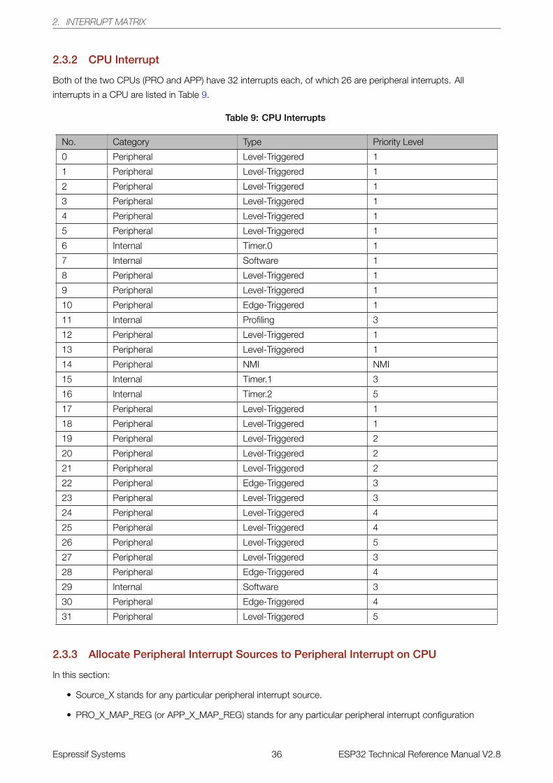
Both of the two CPUs (PRO and APP) have 32 interrupts each, of which 26 are peripheral interrupts. All
interrupts in a CPU are listed in Table 9.
Table 9: CPU Interrupts
No. Category Type Priority Level
0 Peripheral Level-Triggered 1
1 Peripheral Level-Triggered 1
2 Peripheral Level-Triggered 1
3 Peripheral Level-Triggered 1
4 Peripheral Level-Triggered 1
5 Peripheral Level-Triggered 1
6 Internal Timer.0 1
7 Internal Software 1
8 Peripheral Level-Triggered 1
9 Peripheral Level-Triggered 1
10 Peripheral Edge-Triggered 1
11 Internal Profiling 3
12 Peripheral Level-Triggered 1
13 Peripheral Level-Triggered 1
14 Peripheral NMI NMI
15 Internal Timer.1 3
16 Internal Timer.2 5
17 Peripheral Level-Triggered 1
18 Peripheral Level-Triggered 1
19 Peripheral Level-Triggered 2
20 Peripheral Level-Triggered 2
21 Peripheral Level-Triggered 2
22 Peripheral Edge-Triggered 3
23 Peripheral Level-Triggered 3
24 Peripheral Level-Triggered 4
25 Peripheral Level-Triggered 4
26 Peripheral Level-Triggered 5
27 Peripheral Level-Triggered 3
28 Peripheral Edge-Triggered 4
29 Internal Software 3
30 Peripheral Edge-Triggered 4
31 Peripheral Level-Triggered 5
2.3.3 Allocate Peripheral Interrupt Sources to Peripheral Interrupt on CPU
In this section:
• Source_X stands for any particular peripheral interrupt source.
• PRO_X_MAP_REG (or APP_X_MAP_REG) stands for any particular peripheral interrupt configuration
Espressif Systems 36 ESP32 Technical Reference Manual V2.8
2. INTERRUPT MATRIX
register of the PRO_CPU (or APP_CPU). The peripheral interrupt configuration register corresponds to the
peripheral interrupt source Source_X. In Table 8 the registers listed under “PRO_CPU (APP_CPU) -
Peripheral Interrupt Configuration Register” correspond to the peripheral interrupt sources listed in
“Peripheral Interrupt Source - Name”.
• Interrupt_P stands for CPU peripheral interrupt, numbered as Num_P. Num_P can take the ranges 0 ~ 5, 8
~ 10, 12 ~ 14, 17 ~ 28, 30 ~ 31.
• Interrupt_I stands for the CPU internal interrupt numbered as Num_I. Num_I can take values 6, 7, 11, 15,
16, 29.
Using this terminology, the possible operations of the Interrupt Matrix controller can be described as
follows:
• Allocate peripheral interrupt source Source_X to CPU (PRO_CPU or APP_CPU)
Set PRO_X_MAP_REG�or APP_X_MAP_REG�to Num_P. Num_P can be any CPU peripheral interrupt
number. CPU interrupts can be shared between multiple peripherals (see below).
• Disable peripheral interrupt source Source_X for CPU (PRO_CPU or APP_CPU)
Set PRO_X_MAP_REG�or APP_X _MAP_REG�for peripheral interrupt source to any Num_I. The specific
choice of internal interrupt number does not change behaviour, as none of the interrupt numbered as
Num_I is connected to either CPU.
• Allocate multiple peripheral sources Source_Xn ORed to PRO_CPU (APP_CPU) peripheral interrupt
Set multiple PRO_Xn_MAP_REG (APP_Xn_MAP_REG) to the same Num_P. Any of these peripheral
interrupts will trigger CPU Interrupt_P.
2.3.4 CPU NMI Interrupt Mask
The Interrupt Matrix temporarily masks all peripheral interrupt sources allocated to PRO_CPU’s ( or APP_CPU’s )
NMI interrupt, if it receives the signal PRO_CPU NMI Interrupt Mask ( or APP_CPU NMI Interrupt Mask ) from the
peripheral PID Controller, respectively.
2.3.5 Query Current Interrupt Status of Peripheral Interrupt Source
The current interrupt status of a peripheral interrupt source can be read via the bit value in
PRO_INTR_STATUS_REG_n (APP_INTR_STATUS_REG_n), as shown in the mapping in Table 8.
Espressif Systems 37 ESP32 Technical Reference Manual V2.8
3. RESET AND CLOCK
3. Reset and Clock
3.1 System Reset
3.1.1 Introduction
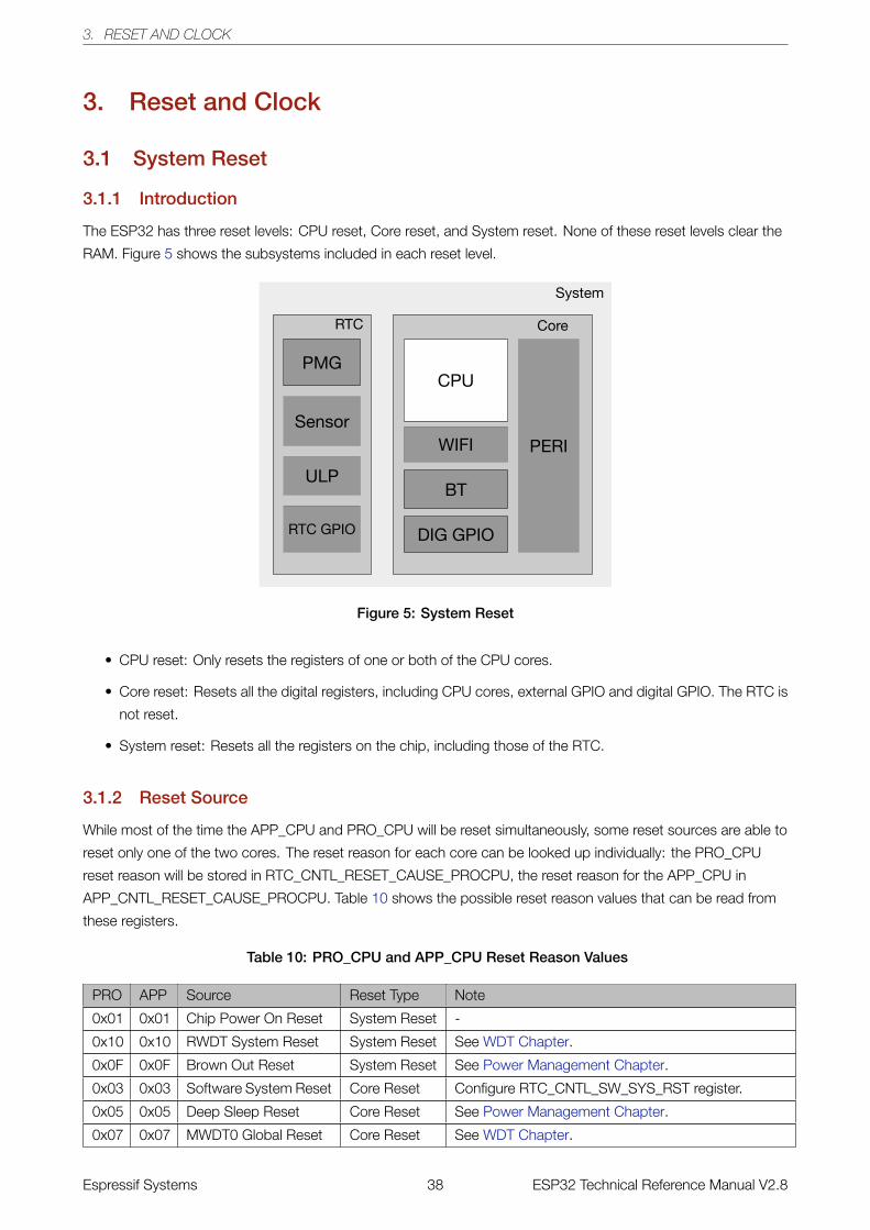
The ESP32 has three reset levels: CPU reset, Core reset, and System reset. None of these reset levels clear the
RAM. Figure 5 shows the subsystems included in each reset level.
Figure 5: System Reset
• CPU reset: Only resets the registers of one or both of the CPU cores.
• Core reset: Resets all the digital registers, including CPU cores, external GPIO and digital GPIO. The RTC is
not reset.
• System reset: Resets all the registers on the chip, including those of the RTC.
3.1.2 Reset Source
While most of the time the APP_CPU and PRO_CPU will be reset simultaneously, some reset sources are able to
reset only one of the two cores. The reset reason for each core can be looked up individually: the PRO_CPU
reset reason will be stored in RTC_CNTL_RESET_CAUSE_PROCPU, the reset reason for the APP_CPU in
APP_CNTL_RESET_CAUSE_PROCPU. Table 10 shows the possible reset reason values that can be read from
these registers.
Table 10: PRO_CPU and APP_CPU Reset Reason Values
PRO APP Source Reset Type Note
0x01 0x01 Chip Power On Reset System Reset -
0x10 0x10 RWDT System Reset System Reset See WDT Chapter.
0x0F 0x0F Brown Out Reset System Reset See Power Management Chapter.
0x03 0x03 Software System Reset Core Reset Configure RTC_CNTL_SW_SYS_RST register.
0x05 0x05 Deep Sleep Reset Core Reset See Power Management Chapter.
0x07 0x07 MWDT0 Global Reset Core Reset See WDT Chapter.
Espressif Systems 38 ESP32 Technical Reference Manual V2.8
3. RESET AND CLOCK
PRO APP APP Source Reset Type Note
0x08 0x08 MWDT1 Global Reset Core Reset See WDT Chapter.
0x09 0x09 RWDT Core Reset Core Reset See WDT Chapter.
0x0B - MWDT0 CPU Reset CPU Reset See WDT Chapter.
0x0C - Software CPU Reset CPU Reset Configure RTC_CNTL_SW_APPCPU_RST register.
- 0x0B MWDT1 CPU Reset CPU Reset See WDT Chapter.
- 0x0C Software CPU Reset CPU Reset Configure RTC_CNTL_SW_APPCPU_RST register.
0x0D 0x0D RWDT CPU Reset CPU Reset See WDT Chapter.
- 0xE PRO CPU Reset CPU Reset
Indicates that the PRO CPU has indepen-
dently reset the APP CPU by configuring the
DPORT_APPCPU_RESETTING register.
3.2 System Clock
3.2.1 Introduction
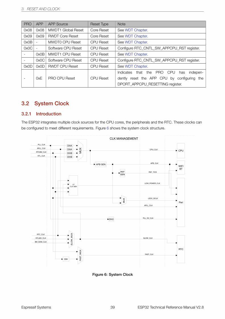
The ESP32 integrates multiple clock sources for the CPU cores, the peripherals and the RTC. These clocks can
be configured to meet different requirements. Figure 6 shows the system clock structure.
Figure 6: System Clock
Espressif Systems 39 ESP32 Technical Reference Manual V2.8
3. RESET AND CLOCK
3.2.2 Clock Source
The ESP32 can use an external crystal oscillator, an internal PLL or an oscillating circuit as a clock source.
Specifically, the clock sources available are:
• High Speed Clocks
– PLL_CLK is an internal PLL clock with a frequency of 320 MHz.
– XTL_CLK is a clock signal generated using an external crystal with a frequency range of 2 ~ 40 MHz.
• Low Power Clocks
– XTL32K_CLK is a clock generated using an external crystal with a frequency of 32 KHz.
– RTC8M_CLK is an internal clock with a default frequency of 8 MHz. This frequency is adjustable.
– RTC8M_D256_CLK is divided from RTC8M_CLK 256. Its frequency is (RTC8M_CLK / 256). With the
default RTC8M_CLK frequency of 8 MHz, this clock runs at 31.250 KHz.
– RTC_CLK is an internal low power clock with a default frequency of 150 KHz. This frequency is
adjustable.
• Audio Clock
– APLL_CLK is an internal Audio PLL clock with a frequency range of 16 ~ 128 MHz.
3.2.3 CPU Clock
As Figure 6 shows, CPU_CLK is the master clock for both CPU cores. CPU_CLK clock can be as high as 160
MHz when the CPU is in high performance mode. Alternatively, the CPU can run at lower frequencies to reduce
power consumption.
The CPU_CLK clock source is determined by the RTC_CNTL_SOC_CLK_SEL register. PLL_CLK, APLL_CLK,
RTC8M_CLK and XTL_CLK can be set as the CPU_CLK source; see Table 11 and 12.
Table 11: CPU_CLK Source
RTC_CNTL_SOC_CLK_SEL Value Clock Source
0 XTL_CLK
1 PLL_CLK
2 RTC8M_CLK
3 APLL_CLK
Espressif Systems 40 ESP32 Technical Reference Manual V2.8
3. RESET AND CLOCK
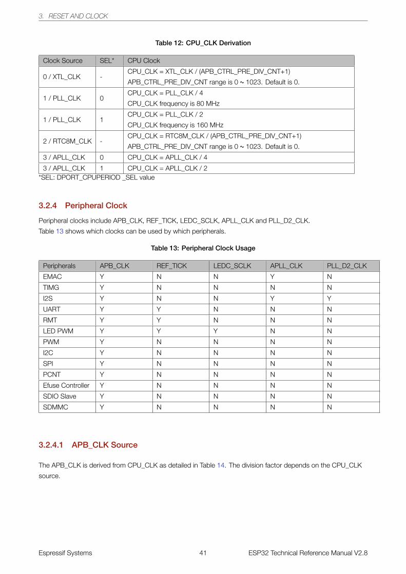
Table 12: CPU_CLK Derivation
Clock Source SEL* CPU Clock
0 / XTL_CLK -CPU_CLK = XTL_CLK / (APB_CTRL_PRE_DIV_CNT+1)
APB_CTRL_PRE_DIV_CNT range is 0 ~ 1023. Default is 0.
1 / PLL_CLK 0CPU_CLK = PLL_CLK / 4
CPU_CLK frequency is 80 MHz
1 / PLL_CLK 1CPU_CLK = PLL_CLK / 2
CPU_CLK frequency is 160 MHz
2 / RTC8M_CLK -CPU_CLK = RTC8M_CLK / (APB_CTRL_PRE_DIV_CNT+1)
APB_CTRL_PRE_DIV_CNT range is 0 ~ 1023. Default is 0.
3 / APLL_CLK 0 CPU_CLK = APLL_CLK / 4
3 / APLL_CLK 1 CPU_CLK = APLL_CLK / 2*SEL: DPORT_CPUPERIOD _SEL value
3.2.4 Peripheral Clock
Peripheral clocks include APB_CLK, REF_TICK, LEDC_SCLK, APLL_CLK and PLL_D2_CLK.
Table 13 shows which clocks can be used by which peripherals.
Table 13: Peripheral Clock Usage
Peripherals APB_CLK REF_TICK LEDC_SCLK APLL_CLK PLL_D2_CLK
EMAC Y N N Y N
TIMG Y N N N N
I2S Y N N Y Y
UART Y Y N N N
RMT Y Y N N N
LED PWM Y Y Y N N
PWM Y N N N N
I2C Y N N N N
SPI Y N N N N
PCNT Y N N N N
Efuse Controller Y N N N N
SDIO Slave Y N N N N
SDMMC Y N N N N
3.2.4.1 APB_CLK Source
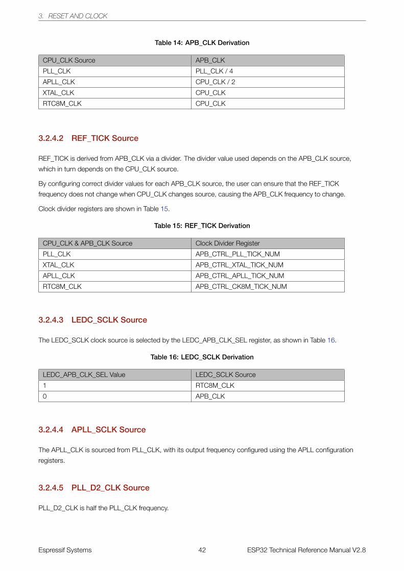
The APB_CLK is derived from CPU_CLK as detailed in Table 14. The division factor depends on the CPU_CLK
source.
Espressif Systems 41 ESP32 Technical Reference Manual V2.8
3. RESET AND CLOCK
Table 14: APB_CLK Derivation
CPU_CLK Source APB_CLK
PLL_CLK PLL_CLK / 4
APLL_CLK CPU_CLK / 2
XTAL_CLK CPU_CLK
RTC8M_CLK CPU_CLK
3.2.4.2 REF_TICK Source
REF_TICK is derived from APB_CLK via a divider. The divider value used depends on the APB_CLK source,
which in turn depends on the CPU_CLK source.
By configuring correct divider values for each APB_CLK source, the user can ensure that the REF_TICK
frequency does not change when CPU_CLK changes source, causing the APB_CLK frequency to change.
Clock divider registers are shown in Table 15.
Table 15: REF_TICK Derivation
CPU_CLK & APB_CLK Source Clock Divider Register
PLL_CLK APB_CTRL_PLL_TICK_NUM
XTAL_CLK APB_CTRL_XTAL_TICK_NUM
APLL_CLK APB_CTRL_APLL_TICK_NUM
RTC8M_CLK APB_CTRL_CK8M_TICK_NUM
3.2.4.3 LEDC_SCLK Source
The LEDC_SCLK clock source is selected by the LEDC_APB_CLK_SEL register, as shown in Table 16.
Table 16: LEDC_SCLK Derivation
LEDC_APB_CLK_SEL Value LEDC_SCLK Source
1 RTC8M_CLK
0 APB_CLK
3.2.4.4 APLL_SCLK Source
The APLL_CLK is sourced from PLL_CLK, with its output frequency configured using the APLL configuration
registers.
3.2.4.5 PLL_D2_CLK Source
PLL_D2_CLK is half the PLL_CLK frequency.
Espressif Systems 42 ESP32 Technical Reference Manual V2.8
3. RESET AND CLOCK
3.2.4.6 Clock Source Considerations
Most peripherals will operate using the APB_CLK frequency as a reference. When this frequency changes, the
peripherals will need to update their clock configuration to operate at the same frequency after the change.
Peripherals accessing REF_TICK can continue operating normally when switching clock sources, without
changing clock source. Please see Table 13 for details.
The LED PWM module can use RTC8M_CLK as a clock source when APB_CLK is disabled. In other words,
when the system is in low-power consumption mode (see Power Management Chapter), normal peripherals will
be halted (APB_CLK is turned off), but the LED PWM can work normally via RTC8M_CLK.
3.2.5 Wi-Fi BT Clock
Wi-Fi and BT can only operate if APB_CLK uses PLL_CLK as its clock source. Suspending PLL_CLK requires
Wi-Fi and BT to both have entered low-power consumption mode first.
For LOW_POWER_CLK, one of RTC_CLK, SLOW_CLK, RTC8M_CLK or XTL_CLK can be selected as the
low-power consumption mode clock source for Wi-Fi and BT.
3.2.6 RTC Clock
The clock sources of SLOW_CLK and FAST_CLK are low-frequency clocks. The RTC module can operate when
most other clocks are stopped.
SLOW_CLK is used to clock the Power Management module. It can be sourced from RTC_CLK, XTL32K_CLK
or RTC8M_D256_CLK
FAST_CLK is used to clock the On-chip Sensor module. It can be sourced from a divided XTL_CLK or from
RTC8M_CLK.
3.2.7 Audio PLL
The operation of audio and other time-critical data-transfer applications requires highly-configurable, low-jitter,
and accurate clock sources. The clock sources derived from system clocks that serve digital peripherals may
carry jitter and, therefore, they do not support a high-precision clock frequency setting.
Providing an integrated precision clock source can minimize system cost. To this end, ESP32 integrates an audio
PLL intended for I2S peripherals. More details on how to clock the I2S module, using an APLL clock, can be
found in Chapter I2S. The Audio PLL formula is as follows:
fout =fxtal(sdm2 + sdm1
28 + sdm0216 + 4)
2(odir + 2)
The parameters of this formula are defined below:
• fxtal: the frequency of the crystal oscillator, usually 40 MHz;
• sdm0: the value is 0 ~ 255;
• sdm1: the value is 0 ~ 255;
• sdm2: the value is 0 ~ 63;
• odir: the value is 0 ~ 31;
Espressif Systems 43 ESP32 Technical Reference Manual V2.8
3. RESET AND CLOCK
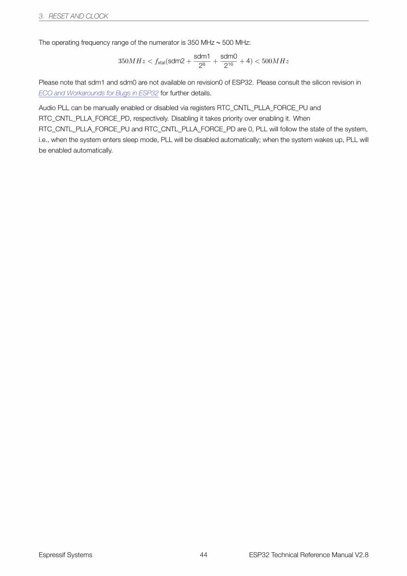
The operating frequency range of the numerator is 350 MHz ~ 500 MHz:
350MHz < fxtal(sdm2 +sdm1
28 +sdm0216 + 4) < 500MHz
Please note that sdm1 and sdm0 are not available on revision0 of ESP32. Please consult the silicon revision in
ECO and Workarounds for Bugs in ESP32 for further details.
Audio PLL can be manually enabled or disabled via registers RTC_CNTL_PLLA_FORCE_PU and
RTC_CNTL_PLLA_FORCE_PD, respectively. Disabling it takes priority over enabling it. When
RTC_CNTL_PLLA_FORCE_PU and RTC_CNTL_PLLA_FORCE_PD are 0, PLL will follow the state of the system,
i.e., when the system enters sleep mode, PLL will be disabled automatically; when the system wakes up, PLL will
be enabled automatically.
Espressif Systems 44 ESP32 Technical Reference Manual V2.8
4. IO_MUX AND GPIO MATRIX
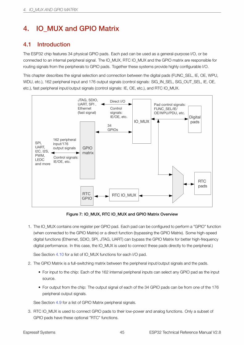
4. IO_MUX and GPIO Matrix
4.1 Introduction
The ESP32 chip features 34 physical GPIO pads. Each pad can be used as a general-purpose I/O, or be
connected to an internal peripheral signal. The IO_MUX, RTC IO_MUX and the GPIO matrix are responsible for
routing signals from the peripherals to GPIO pads. Together these systems provide highly configurable I/O.
This chapter describes the signal selection and connection between the digital pads (FUNC_SEL, IE, OE, WPU,
WDU, etc.), 162 peripheral input and 176 output signals (control signals: SIG_IN_SEL, SIG_OUT_SEL, IE, OE,
etc.), fast peripheral input/output signals (control signals: IE, OE, etc.), and RTC IO_MUX.
Figure 7: IO_MUX, RTC IO_MUX and GPIO Matrix Overview
1. The IO_MUX contains one register per GPIO pad. Each pad can be configured to perform a ”GPIO” function
(when connected to the GPIO Matrix) or a direct function (bypassing the GPIO Matrix). Some high-speed
digital functions (Ethernet, SDIO, SPI, JTAG, UART) can bypass the GPIO Matrix for better high-frequency
digital performance. In this case, the IO_MUX is used to connect these pads directly to the peripheral.)
See Section 4.10 for a list of IO_MUX functions for each I/O pad.
2. The GPIO Matrix is a full-switching matrix between the peripheral input/output signals and the pads.
• For input to the chip: Each of the 162 internal peripheral inputs can select any GPIO pad as the input
source.
• For output from the chip: The output signal of each of the 34 GPIO pads can be from one of the 176
peripheral output signals.
See Section 4.9 for a list of GPIO Matrix peripheral signals.
3. RTC IO_MUX is used to connect GPIO pads to their low-power and analog functions. Only a subset of
GPIO pads have these optional ”RTC” functions.
Espressif Systems 45 ESP32 Technical Reference Manual V2.8
4. IO_MUX AND GPIO MATRIX
See Section 4.11 for a list of RTC IO_MUX functions.
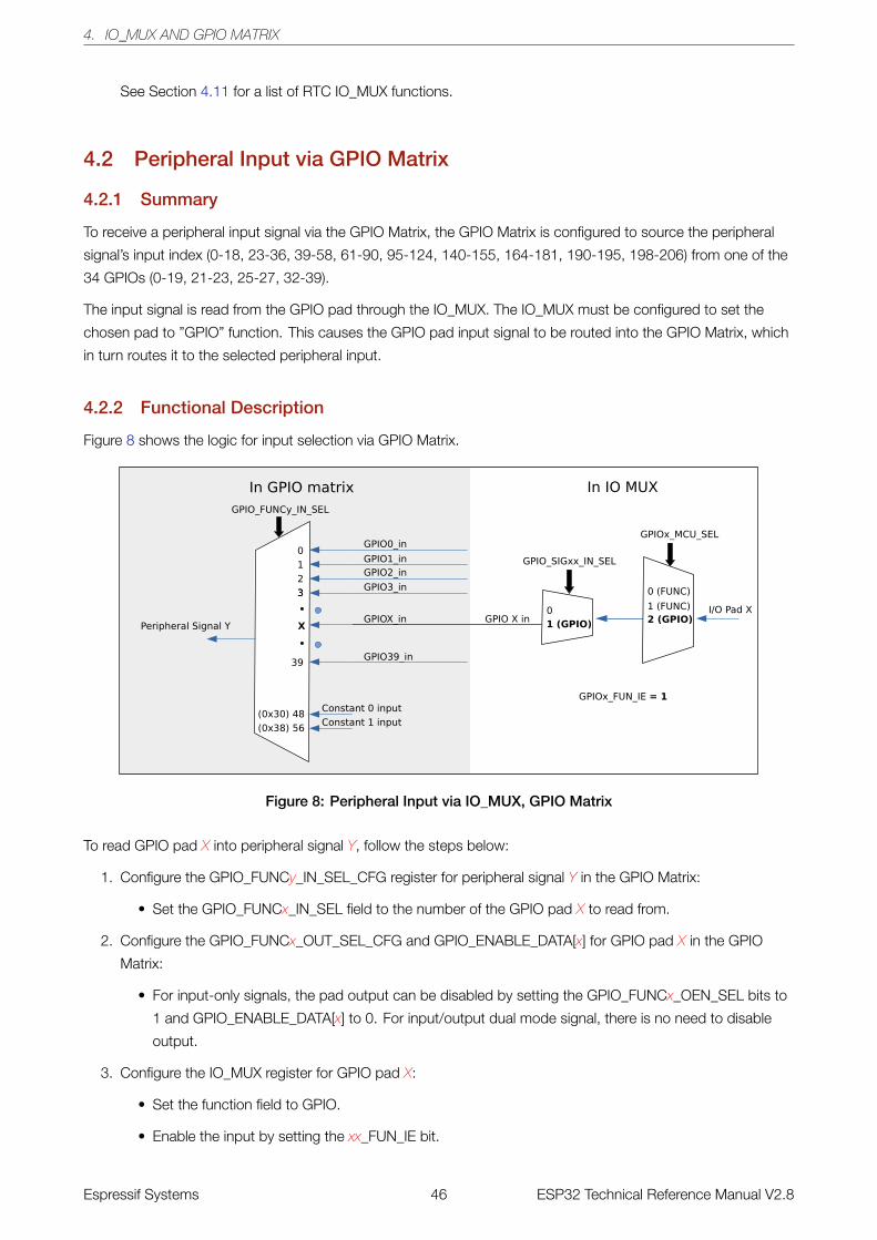
4.2 Peripheral Input via GPIO Matrix
4.2.1 Summary
To receive a peripheral input signal via the GPIO Matrix, the GPIO Matrix is configured to source the peripheral
signal’s input index (0-18, 23-36, 39-58, 61-90, 95-124, 140-155, 164-181, 190-195, 198-206) from one of the
34 GPIOs (0-19, 21-23, 25-27, 32-39).
The input signal is read from the GPIO pad through the IO_MUX. The IO_MUX must be configured to set the
chosen pad to ”GPIO” function. This causes the GPIO pad input signal to be routed into the GPIO Matrix, which
in turn routes it to the selected peripheral input.
4.2.2 Functional Description
Figure 8 shows the logic for input selection via GPIO Matrix.
GPIO_FUNCy_IN_SEL
GPIO0_in
GPIO1_in
GPIO2_in
GPIO3_in
GPIO39_in
0 (FUNC)
1 (FUNC)
2 (GPIO)
3
39
Peripheral Signal Y
I/O Pad X
In GPIO matrix In IO MUX
GPIO X in
GPIOx_MCU_SEL
2
1
3
XGPIOX_in
0
Constant 0 input
Constant 1 input(0x30) 48
(0x38) 56
0
1 (GPIO)
GPIO_SIGxx_IN_SEL
GPIOx_FUN_IE = 1
Figure 8: Peripheral Input via IO_MUX, GPIO Matrix
To read GPIO pad X into peripheral signal Y, follow the steps below:
1. Configure the GPIO_FUNCy_IN_SEL_CFG register for peripheral signal Y in the GPIO Matrix:
• Set the GPIO_FUNCx_IN_SEL field to the number of the GPIO pad X to read from.
2. Configure the GPIO_FUNCx_OUT_SEL_CFG and GPIO_ENABLE_DATA[x] for GPIO pad X in the GPIO
Matrix:
• For input-only signals, the pad output can be disabled by setting the GPIO_FUNCx_OEN_SEL bits to
1 and GPIO_ENABLE_DATA[x] to 0. For input/output dual mode signal, there is no need to disable
output.
3. Configure the IO_MUX register for GPIO pad X:
• Set the function field to GPIO.
• Enable the input by setting the xx_FUN_IE bit.
Espressif Systems 46 ESP32 Technical Reference Manual V2.8
4. IO_MUX AND GPIO MATRIX
• Set xx_FUN_WPU and xx_FUN_WPD fields, as required, to enable internal pull-up/pull-down resistors.
Notes:
• One input pad can be connected to multiple input_signals.
• The input signal can be inverted with GPIO_FUNCx_IN_INV_SEL.
• It is possible to have a peripheral read a constantly low or constantly high input value without connecting
this input to a pad. This can be done by selecting a special GPIO_FUNCy_IN_SEL input, instead of a GPIO
number:
– When GPIO_FUNCx_IN_SEL is 0x30, input_signal_x is always 0.
– When GPIO_FUNCx_IN_SEL is 0x38, input_signal_x is always 1.
4.2.3 Simple GPIO Input
The GPIO_IN_REG/GPIO_IN1_REG register holds the input values of each GPIO pad.
The input value of any GPIO pin can be read at any time without configuring the GPIO Matrix for a particular
peripheral signal. However, it is necessary to configure the xx_FUN_IE register for pad X, as shown in Section
4.2.2.
4.3 Peripheral Output via GPIO Matrix
4.3.1 Summary
To output a signal from a peripheral via the GPIO Matrix, the GPIO Matrix is configured to route the peripheral
output signal (0-18, 23-37, 61-121, 140-125, 224-228) to one of the 34 GPIOs (0-19, 21-23, 25-27,
32-39).
The output signal is routed from the peripheral into the GPIO Matrix. It is then routed into the IO_MUX, which is
configured to set the chosen pad to ”GPIO” function. This causes the output GPIO signal to be connected to the
pad.
Note:
The peripheral output signals 224 to 228 can be configured to be routed in from one GPIO and output directly from another
GPIO.
4.3.2 Functional Description
One of the 176 output signals can be selected to go through the GPIO matrix into the IO_MUX and then to a pad.
Figure 9 illustrates the configuration.
To output peripheral signal Y to particular GPIO pad X, follow these steps:
1. Configure the GPIO_FUNCx_OUT_SEL_CFG register and GPIO_ENABLE_DATA[x] of GPIO X in the GPIO
Matrix:
• Set GPIO_FUNCx_OUT_SEL to the index of required peripheral output signal Y.
Espressif Systems 47 ESP32 Technical Reference Manual V2.8
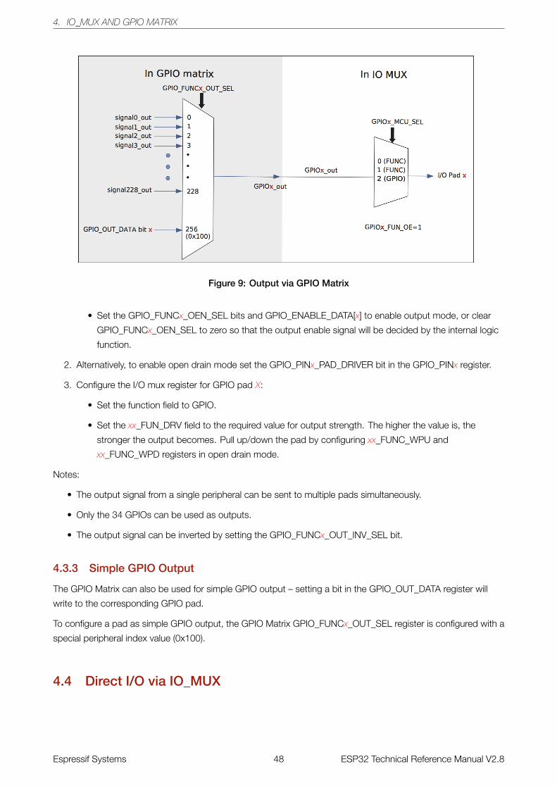
4. IO_MUX AND GPIO MATRIX
Figure 9: Output via GPIO Matrix
• Set the GPIO_FUNCx_OEN_SEL bits and GPIO_ENABLE_DATA[x] to enable output mode, or clear
GPIO_FUNCx_OEN_SEL to zero so that the output enable signal will be decided by the internal logic
function.
2. Alternatively, to enable open drain mode set the GPIO_PINx_PAD_DRIVER bit in the GPIO_PINx register.
3. Configure the I/O mux register for GPIO pad X:
• Set the function field to GPIO.
• Set the xx_FUN_DRV field to the required value for output strength. The higher the value is, the
stronger the output becomes. Pull up/down the pad by configuring xx_FUNC_WPU and
xx_FUNC_WPD registers in open drain mode.
Notes:
• The output signal from a single peripheral can be sent to multiple pads simultaneously.
• Only the 34 GPIOs can be used as outputs.
• The output signal can be inverted by setting the GPIO_FUNCx_OUT_INV_SEL bit.
4.3.3 Simple GPIO Output
The GPIO Matrix can also be used for simple GPIO output – setting a bit in the GPIO_OUT_DATA register will
write to the corresponding GPIO pad.
To configure a pad as simple GPIO output, the GPIO Matrix GPIO_FUNCx_OUT_SEL register is configured with a
special peripheral index value (0x100).
4.4 Direct I/O via IO_MUX
Espressif Systems 48 ESP32 Technical Reference Manual V2.8
4. IO_MUX AND GPIO MATRIX
4.4.1 Summary
Some high speed digital functions (Ethernet, SDIO, SPI, JTAG, UART) can bypass the GPIO Matrix for better
high-frequency digital performance. In this case, the IO_MUX is used to connect these pads directly to the
peripheral.
Selecting this option is less flexible than using the GPIO Matrix, as the IO_MUX register for each GPIO pad can
only select from a limited number of functions. However, better high-frequency digital performance will be
maintained.
4.4.2 Functional Description
Two registers must be configured in order to bypass the GPIO Matrix for peripheral I/O:
1. IO_MUX for the GPIO pad must be set to the required pad function. (Please refer to section 4.10 for a list of
pad functions.)
2. For inputs, the SIG_IN_SEL register must be set to route the input directly to the peripheral.
4.5 RTC IO_MUX for Low Power and Analog I/O
4.5.1 Summary
18 GPIO pads have low power capabilities (RTC domain) and analog functions which are handled by the RTC
subsystem of ESP32. The IO_MUX and GPIO Matrix are not used for these functions; rather, the RTC_MUX is
used to redirect the I/O to the RTC subsystem.
When configured as RTC GPIOs, the output pads can still retain the output level value when the chip is in
Deep-sleep mode, and the input pads can wake up the chip from Deep-sleep.
Section 4.11 has a list of RTC_MUX pins and their functions.
4.5.2 Functional Description
Each pad with analog and RTC functions is controlled by the RTC_IO_TOUCH_PADx_TO_GPIO bit in the
RTC_GPIO_PINx register. By default this bit is set to 1, routing all I/O via the IO_MUX subsystem as described in
earlier subsections.
If the RTC_IO_TOUCH_PADx_TO_GPIO bit is cleared, then I/O to and from that pad is routed to the RTC
subsystem. In this mode, the RTC_GPIO_PINx register is used for digital I/O and the analog features of the pad
are also available. See Section 4.11 for a list of RTC pin functions.
See 4.11 for a table mapping GPIO pads to their RTC equivalent pins and analog functions. Note that the
RTC_IO_PINx registers use the RTC GPIO pin numbering, not the GPIO pad numbering.
Espressif Systems 49 ESP32 Technical Reference Manual V2.8
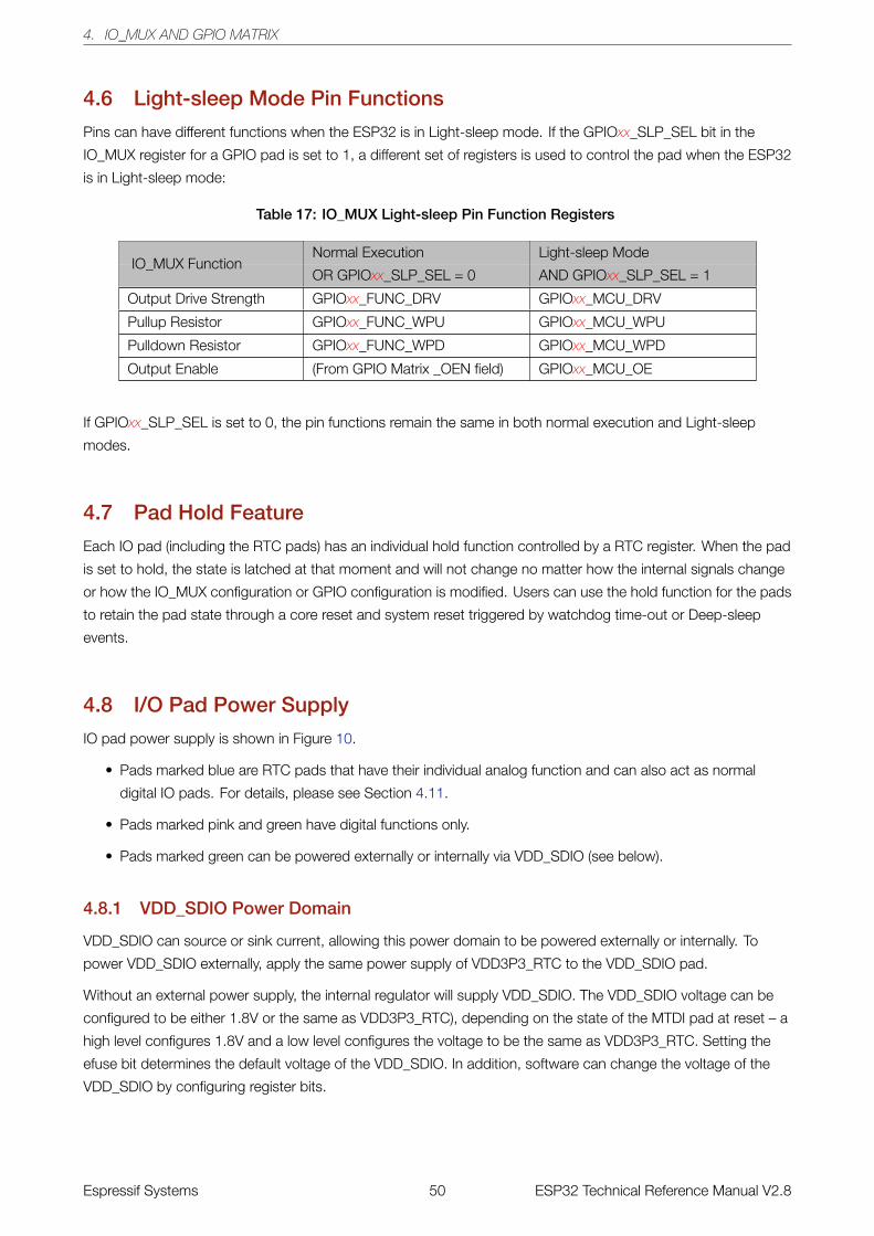
4. IO_MUX AND GPIO MATRIX
4.6 Light-sleep Mode Pin Functions
Pins can have different functions when the ESP32 is in Light-sleep mode. If the GPIOxx_SLP_SEL bit in the
IO_MUX register for a GPIO pad is set to 1, a different set of registers is used to control the pad when the ESP32
is in Light-sleep mode:
Table 17: IO_MUX Light-sleep Pin Function Registers
Normal Execution Light-sleep ModeIO_MUX Function
OR GPIOxx_SLP_SEL = 0 AND GPIOxx_SLP_SEL = 1
Output Drive Strength GPIOxx_FUNC_DRV GPIOxx_MCU_DRV
Pullup Resistor GPIOxx_FUNC_WPU GPIOxx_MCU_WPU
Pulldown Resistor GPIOxx_FUNC_WPD GPIOxx_MCU_WPD
Output Enable (From GPIO Matrix _OEN field) GPIOxx_MCU_OE
If GPIOxx_SLP_SEL is set to 0, the pin functions remain the same in both normal execution and Light-sleep
modes.
4.7 Pad Hold Feature
Each IO pad (including the RTC pads) has an individual hold function controlled by a RTC register. When the pad
is set to hold, the state is latched at that moment and will not change no matter how the internal signals change
or how the IO_MUX configuration or GPIO configuration is modified. Users can use the hold function for the pads
to retain the pad state through a core reset and system reset triggered by watchdog time-out or Deep-sleep
events.
4.8 I/O Pad Power Supply
IO pad power supply is shown in Figure 10.
• Pads marked blue are RTC pads that have their individual analog function and can also act as normal
digital IO pads. For details, please see Section 4.11.
• Pads marked pink and green have digital functions only.
• Pads marked green can be powered externally or internally via VDD_SDIO (see below).
4.8.1 VDD_SDIO Power Domain
VDD_SDIO can source or sink current, allowing this power domain to be powered externally or internally. To
power VDD_SDIO externally, apply the same power supply of VDD3P3_RTC to the VDD_SDIO pad.
Without an external power supply, the internal regulator will supply VDD_SDIO. The VDD_SDIO voltage can be
configured to be either 1.8V or the same as VDD3P3_RTC), depending on the state of the MTDI pad at reset – a
high level configures 1.8V and a low level configures the voltage to be the same as VDD3P3_RTC. Setting the
efuse bit determines the default voltage of the VDD_SDIO. In addition, software can change the voltage of the
VDD_SDIO by configuring register bits.
Espressif Systems 50 ESP32 Technical Reference Manual V2.8
4. IO_MUX AND GPIO MATRIX
Figure 10: ESP32 I/O Pad Power Sources
4.9 Peripheral Signal List
Table 18 contains a list of Peripheral Input/Output signals used by the GPIO Matrix:
Table 18: GPIO Matrix Peripheral Signals
Signal Input Signal Output Signal Direct I/O in IO_MUX
0 SPICLK_in SPICLK_out YES
1 SPIQ_in SPIQ_out YES
2 SPID_in SPID_out YES
3 SPIHD_in SPIHD_out YES
4 SPIWP_in SPIWP_out YES
5 SPICS0_in SPICS0_out YES
6 SPICS1_in SPICS1_out
7 SPICS2_in SPICS2_out
8 HSPICLK_in HSPICLK_out YES
9 HSPIQ_in HSPIQ_out YES
10 HSPID_in HSPID_out YES
11 HSPICS0_in HSPICS0_out YES
12 HSPIHD_in HSPIHD_out YES
13 HSPIWP_in HSPIWP_out YES
14 U0RXD_in U0TXD_out YES
15 U0CTS_in U0RTS_out YES
16 U0DSR_in U0DTR_out
17 U1RXD_in U1TXD_out YES
18 U1CTS_in U1RTS_out YES
23 I2S0O_BCK_in I2S0O_BCK_out
Espressif Systems 51 ESP32 Technical Reference Manual V2.8
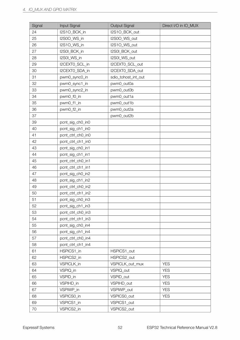
4. IO_MUX AND GPIO MATRIX
Signal Input Signal Output Signal Direct I/O in IO_MUX
24 I2S1O_BCK_in I2S1O_BCK_out
25 I2S0O_WS_in I2S0O_WS_out
26 I2S1O_WS_in I2S1O_WS_out
27 I2S0I_BCK_in I2S0I_BCK_out
28 I2S0I_WS_in I2S0I_WS_out
29 I2CEXT0_SCL_in I2CEXT0_SCL_out
30 I2CEXT0_SDA_in I2CEXT0_SDA_out
31 pwm0_sync0_in sdio_tohost_int_out
32 pwm0_sync1_in pwm0_out0a
33 pwm0_sync2_in pwm0_out0b
34 pwm0_f0_in pwm0_out1a
35 pwm0_f1_in pwm0_out1b
36 pwm0_f2_in pwm0_out2a
37 pwm0_out2b
39 pcnt_sig_ch0_in0
40 pcnt_sig_ch1_in0
41 pcnt_ctrl_ch0_in0
42 pcnt_ctrl_ch1_in0
43 pcnt_sig_ch0_in1
44 pcnt_sig_ch1_in1
45 pcnt_ctrl_ch0_in1
46 pcnt_ctrl_ch1_in1
47 pcnt_sig_ch0_in2
48 pcnt_sig_ch1_in2
49 pcnt_ctrl_ch0_in2
50 pcnt_ctrl_ch1_in2
51 pcnt_sig_ch0_in3
52 pcnt_sig_ch1_in3
53 pcnt_ctrl_ch0_in3
54 pcnt_ctrl_ch1_in3
55 pcnt_sig_ch0_in4
56 pcnt_sig_ch1_in4
57 pcnt_ctrl_ch0_in4
58 pcnt_ctrl_ch1_in4
61 HSPICS1_in HSPICS1_out
62 HSPICS2_in HSPICS2_out
63 VSPICLK_in VSPICLK_out_mux YES
64 VSPIQ_in VSPIQ_out YES
65 VSPID_in VSPID_out YES
66 VSPIHD_in VSPIHD_out YES
67 VSPIWP_in VSPIWP_out YES
68 VSPICS0_in VSPICS0_out YES
69 VSPICS1_in VSPICS1_out
70 VSPICS2_in VSPICS2_out
Espressif Systems 52 ESP32 Technical Reference Manual V2.8
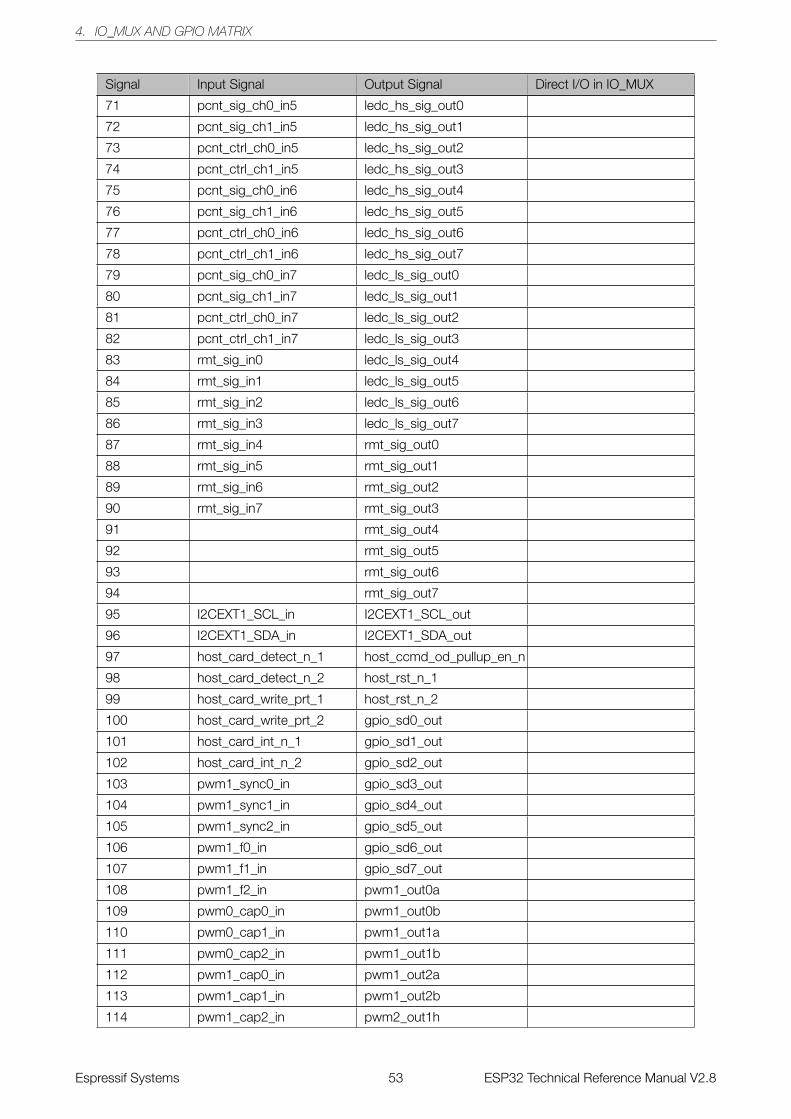
4. IO_MUX AND GPIO MATRIX
Signal Input Signal Output Signal Direct I/O in IO_MUX
71 pcnt_sig_ch0_in5 ledc_hs_sig_out0
72 pcnt_sig_ch1_in5 ledc_hs_sig_out1
73 pcnt_ctrl_ch0_in5 ledc_hs_sig_out2
74 pcnt_ctrl_ch1_in5 ledc_hs_sig_out3
75 pcnt_sig_ch0_in6 ledc_hs_sig_out4
76 pcnt_sig_ch1_in6 ledc_hs_sig_out5
77 pcnt_ctrl_ch0_in6 ledc_hs_sig_out6
78 pcnt_ctrl_ch1_in6 ledc_hs_sig_out7
79 pcnt_sig_ch0_in7 ledc_ls_sig_out0
80 pcnt_sig_ch1_in7 ledc_ls_sig_out1
81 pcnt_ctrl_ch0_in7 ledc_ls_sig_out2
82 pcnt_ctrl_ch1_in7 ledc_ls_sig_out3
83 rmt_sig_in0 ledc_ls_sig_out4
84 rmt_sig_in1 ledc_ls_sig_out5
85 rmt_sig_in2 ledc_ls_sig_out6
86 rmt_sig_in3 ledc_ls_sig_out7
87 rmt_sig_in4 rmt_sig_out0
88 rmt_sig_in5 rmt_sig_out1
89 rmt_sig_in6 rmt_sig_out2
90 rmt_sig_in7 rmt_sig_out3
91 rmt_sig_out4
92 rmt_sig_out5
93 rmt_sig_out6
94 rmt_sig_out7
95 I2CEXT1_SCL_in I2CEXT1_SCL_out
96 I2CEXT1_SDA_in I2CEXT1_SDA_out
97 host_card_detect_n_1 host_ccmd_od_pullup_en_n
98 host_card_detect_n_2 host_rst_n_1
99 host_card_write_prt_1 host_rst_n_2
100 host_card_write_prt_2 gpio_sd0_out
101 host_card_int_n_1 gpio_sd1_out
102 host_card_int_n_2 gpio_sd2_out
103 pwm1_sync0_in gpio_sd3_out
104 pwm1_sync1_in gpio_sd4_out
105 pwm1_sync2_in gpio_sd5_out
106 pwm1_f0_in gpio_sd6_out
107 pwm1_f1_in gpio_sd7_out
108 pwm1_f2_in pwm1_out0a
109 pwm0_cap0_in pwm1_out0b
110 pwm0_cap1_in pwm1_out1a
111 pwm0_cap2_in pwm1_out1b
112 pwm1_cap0_in pwm1_out2a
113 pwm1_cap1_in pwm1_out2b
114 pwm1_cap2_in pwm2_out1h
Espressif Systems 53 ESP32 Technical Reference Manual V2.8
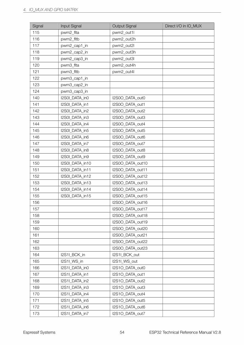
4. IO_MUX AND GPIO MATRIX
Signal Input Signal Output Signal Direct I/O in IO_MUX
115 pwm2_flta pwm2_out1l
116 pwm2_fltb pwm2_out2h
117 pwm2_cap1_in pwm2_out2l
118 pwm2_cap2_in pwm2_out3h
119 pwm2_cap3_in pwm2_out3l
120 pwm3_flta pwm2_out4h
121 pwm3_fltb pwm2_out4l
122 pwm3_cap1_in
123 pwm3_cap2_in
124 pwm3_cap3_in
140 I2S0I_DATA_in0 I2S0O_DATA_out0
141 I2S0I_DATA_in1 I2S0O_DATA_out1
142 I2S0I_DATA_in2 I2S0O_DATA_out2
143 I2S0I_DATA_in3 I2S0O_DATA_out3
144 I2S0I_DATA_in4 I2S0O_DATA_out4
145 I2S0I_DATA_in5 I2S0O_DATA_out5
146 I2S0I_DATA_in6 I2S0O_DATA_out6
147 I2S0I_DATA_in7 I2S0O_DATA_out7
148 I2S0I_DATA_in8 I2S0O_DATA_out8
149 I2S0I_DATA_in9 I2S0O_DATA_out9
150 I2S0I_DATA_in10 I2S0O_DATA_out10
151 I2S0I_DATA_in11 I2S0O_DATA_out11
152 I2S0I_DATA_in12 I2S0O_DATA_out12
153 I2S0I_DATA_in13 I2S0O_DATA_out13
154 I2S0I_DATA_in14 I2S0O_DATA_out14
155 I2S0I_DATA_in15 I2S0O_DATA_out15
156 I2S0O_DATA_out16
157 I2S0O_DATA_out17
158 I2S0O_DATA_out18
159 I2S0O_DATA_out19
160 I2S0O_DATA_out20
161 I2S0O_DATA_out21
162 I2S0O_DATA_out22
163 I2S0O_DATA_out23
164 I2S1I_BCK_in I2S1I_BCK_out
165 I2S1I_WS_in I2S1I_WS_out
166 I2S1I_DATA_in0 I2S1O_DATA_out0
167 I2S1I_DATA_in1 I2S1O_DATA_out1
168 I2S1I_DATA_in2 I2S1O_DATA_out2
169 I2S1I_DATA_in3 I2S1O_DATA_out3
170 I2S1I_DATA_in4 I2S1O_DATA_out4
171 I2S1I_DATA_in5 I2S1O_DATA_out5
172 I2S1I_DATA_in6 I2S1O_DATA_out6
173 I2S1I_DATA_in7 I2S1O_DATA_out7
Espressif Systems 54 ESP32 Technical Reference Manual V2.8
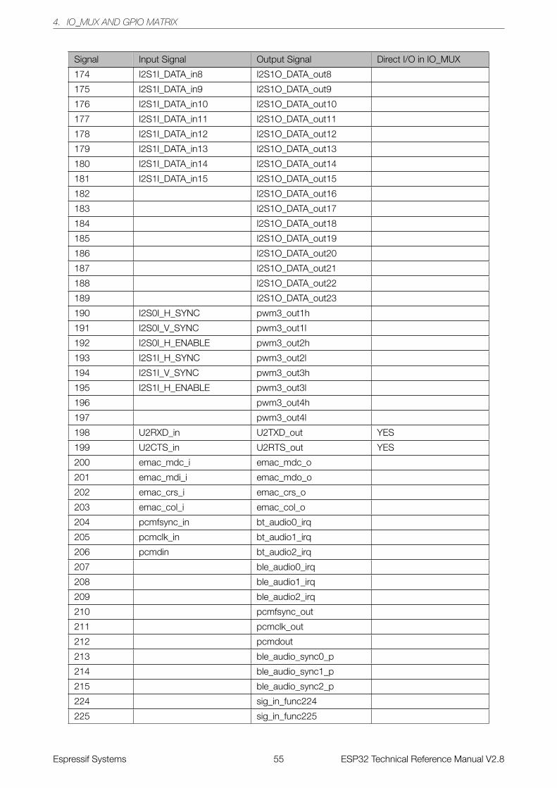
4. IO_MUX AND GPIO MATRIX
Signal Input Signal Output Signal Direct I/O in IO_MUX
174 I2S1I_DATA_in8 I2S1O_DATA_out8
175 I2S1I_DATA_in9 I2S1O_DATA_out9
176 I2S1I_DATA_in10 I2S1O_DATA_out10
177 I2S1I_DATA_in11 I2S1O_DATA_out11
178 I2S1I_DATA_in12 I2S1O_DATA_out12
179 I2S1I_DATA_in13 I2S1O_DATA_out13
180 I2S1I_DATA_in14 I2S1O_DATA_out14
181 I2S1I_DATA_in15 I2S1O_DATA_out15
182 I2S1O_DATA_out16
183 I2S1O_DATA_out17
184 I2S1O_DATA_out18
185 I2S1O_DATA_out19
186 I2S1O_DATA_out20
187 I2S1O_DATA_out21
188 I2S1O_DATA_out22
189 I2S1O_DATA_out23
190 I2S0I_H_SYNC pwm3_out1h
191 I2S0I_V_SYNC pwm3_out1l
192 I2S0I_H_ENABLE pwm3_out2h
193 I2S1I_H_SYNC pwm3_out2l
194 I2S1I_V_SYNC pwm3_out3h
195 I2S1I_H_ENABLE pwm3_out3l
196 pwm3_out4h
197 pwm3_out4l
198 U2RXD_in U2TXD_out YES
199 U2CTS_in U2RTS_out YES
200 emac_mdc_i emac_mdc_o
201 emac_mdi_i emac_mdo_o
202 emac_crs_i emac_crs_o
203 emac_col_i emac_col_o
204 pcmfsync_in bt_audio0_irq
205 pcmclk_in bt_audio1_irq
206 pcmdin bt_audio2_irq
207 ble_audio0_irq
208 ble_audio1_irq
209 ble_audio2_irq
210 pcmfsync_out
211 pcmclk_out
212 pcmdout
213 ble_audio_sync0_p
214 ble_audio_sync1_p
215 ble_audio_sync2_p
224 sig_in_func224
225 sig_in_func225
Espressif Systems 55 ESP32 Technical Reference Manual V2.8
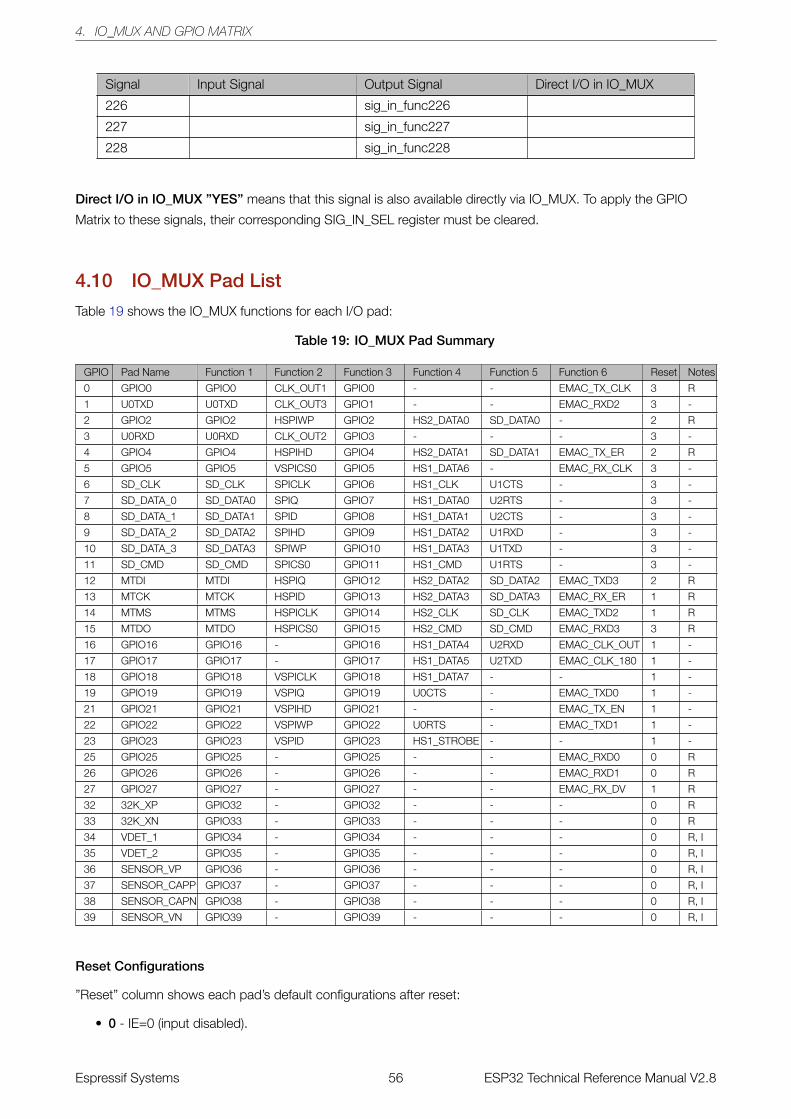
4. IO_MUX AND GPIO MATRIX
Signal Input Signal Output Signal Direct I/O in IO_MUX
226 sig_in_func226
227 sig_in_func227
228 sig_in_func228
Direct I/O in IO_MUX ”YES” means that this signal is also available directly via IO_MUX. To apply the GPIO
Matrix to these signals, their corresponding SIG_IN_SEL register must be cleared.
4.10 IO_MUX Pad List
Table 19 shows the IO_MUX functions for each I/O pad:
Table 19: IO_MUX Pad Summary
GPIO Pad Name Function 1 Function 2 Function 3 Function 4 Function 5 Function 6 Reset Notes
0 GPIO0 GPIO0 CLK_OUT1 GPIO0 - - EMAC_TX_CLK 3 R
1 U0TXD U0TXD CLK_OUT3 GPIO1 - - EMAC_RXD2 3 -
2 GPIO2 GPIO2 HSPIWP GPIO2 HS2_DATA0 SD_DATA0 - 2 R
3 U0RXD U0RXD CLK_OUT2 GPIO3 - - - 3 -
4 GPIO4 GPIO4 HSPIHD GPIO4 HS2_DATA1 SD_DATA1 EMAC_TX_ER 2 R
5 GPIO5 GPIO5 VSPICS0 GPIO5 HS1_DATA6 - EMAC_RX_CLK 3 -
6 SD_CLK SD_CLK SPICLK GPIO6 HS1_CLK U1CTS - 3 -
7 SD_DATA_0 SD_DATA0 SPIQ GPIO7 HS1_DATA0 U2RTS - 3 -
8 SD_DATA_1 SD_DATA1 SPID GPIO8 HS1_DATA1 U2CTS - 3 -
9 SD_DATA_2 SD_DATA2 SPIHD GPIO9 HS1_DATA2 U1RXD - 3 -
10 SD_DATA_3 SD_DATA3 SPIWP GPIO10 HS1_DATA3 U1TXD - 3 -
11 SD_CMD SD_CMD SPICS0 GPIO11 HS1_CMD U1RTS - 3 -
12 MTDI MTDI HSPIQ GPIO12 HS2_DATA2 SD_DATA2 EMAC_TXD3 2 R
13 MTCK MTCK HSPID GPIO13 HS2_DATA3 SD_DATA3 EMAC_RX_ER 1 R
14 MTMS MTMS HSPICLK GPIO14 HS2_CLK SD_CLK EMAC_TXD2 1 R
15 MTDO MTDO HSPICS0 GPIO15 HS2_CMD SD_CMD EMAC_RXD3 3 R
16 GPIO16 GPIO16 - GPIO16 HS1_DATA4 U2RXD EMAC_CLK_OUT 1 -
17 GPIO17 GPIO17 - GPIO17 HS1_DATA5 U2TXD EMAC_CLK_180 1 -
18 GPIO18 GPIO18 VSPICLK GPIO18 HS1_DATA7 - - 1 -
19 GPIO19 GPIO19 VSPIQ GPIO19 U0CTS - EMAC_TXD0 1 -
21 GPIO21 GPIO21 VSPIHD GPIO21 - - EMAC_TX_EN 1 -
22 GPIO22 GPIO22 VSPIWP GPIO22 U0RTS - EMAC_TXD1 1 -
23 GPIO23 GPIO23 VSPID GPIO23 HS1_STROBE - - 1 -
25 GPIO25 GPIO25 - GPIO25 - - EMAC_RXD0 0 R
26 GPIO26 GPIO26 - GPIO26 - - EMAC_RXD1 0 R
27 GPIO27 GPIO27 - GPIO27 - - EMAC_RX_DV 1 R
32 32K_XP GPIO32 - GPIO32 - - - 0 R
33 32K_XN GPIO33 - GPIO33 - - - 0 R
34 VDET_1 GPIO34 - GPIO34 - - - 0 R, I
35 VDET_2 GPIO35 - GPIO35 - - - 0 R, I
36 SENSOR_VP GPIO36 - GPIO36 - - - 0 R, I
37 SENSOR_CAPP GPIO37 - GPIO37 - - - 0 R, I
38 SENSOR_CAPN GPIO38 - GPIO38 - - - 0 R, I
39 SENSOR_VN GPIO39 - GPIO39 - - - 0 R, I
Reset Configurations
”Reset” column shows each pad’s default configurations after reset:
• 0 - IE=0 (input disabled).
Espressif Systems 56 ESP32 Technical Reference Manual V2.8
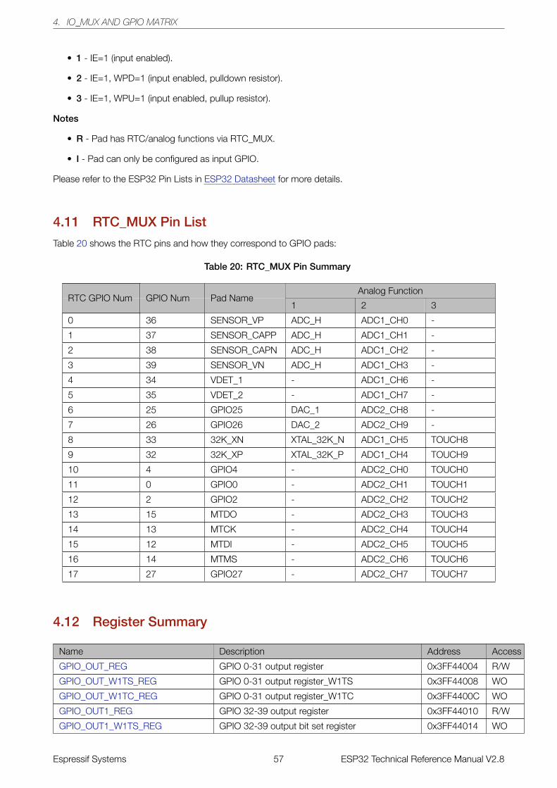
4. IO_MUX AND GPIO MATRIX
• 1 - IE=1 (input enabled).
• 2 - IE=1, WPD=1 (input enabled, pulldown resistor).
• 3 - IE=1, WPU=1 (input enabled, pullup resistor).
Notes
• R - Pad has RTC/analog functions via RTC_MUX.
• I - Pad can only be configured as input GPIO.
Please refer to the ESP32 Pin Lists in ESP32 Datasheet for more details.
4.11 RTC_MUX Pin List
Table 20 shows the RTC pins and how they correspond to GPIO pads:
Table 20: RTC_MUX Pin Summary
Analog FunctionRTC GPIO Num GPIO Num Pad Name
1 2 3
0 36 SENSOR_VP ADC_H ADC1_CH0 -
1 37 SENSOR_CAPP ADC_H ADC1_CH1 -
2 38 SENSOR_CAPN ADC_H ADC1_CH2 -
3 39 SENSOR_VN ADC_H ADC1_CH3 -
4 34 VDET_1 - ADC1_CH6 -
5 35 VDET_2 - ADC1_CH7 -
6 25 GPIO25 DAC_1 ADC2_CH8 -
7 26 GPIO26 DAC_2 ADC2_CH9 -
8 33 32K_XN XTAL_32K_N ADC1_CH5 TOUCH8
9 32 32K_XP XTAL_32K_P ADC1_CH4 TOUCH9
10 4 GPIO4 - ADC2_CH0 TOUCH0
11 0 GPIO0 - ADC2_CH1 TOUCH1
12 2 GPIO2 - ADC2_CH2 TOUCH2
13 15 MTDO - ADC2_CH3 TOUCH3
14 13 MTCK - ADC2_CH4 TOUCH4
15 12 MTDI - ADC2_CH5 TOUCH5
16 14 MTMS - ADC2_CH6 TOUCH6
17 27 GPIO27 - ADC2_CH7 TOUCH7
4.12 Register Summary
Name Description Address Access
GPIO_OUT_REG GPIO 0-31 output register 0x3FF44004 R/W
GPIO_OUT_W1TS_REG GPIO 0-31 output register_W1TS 0x3FF44008 WO
GPIO_OUT_W1TC_REG GPIO 0-31 output register_W1TC 0x3FF4400C WO
GPIO_OUT1_REG GPIO 32-39 output register 0x3FF44010 R/W
GPIO_OUT1_W1TS_REG GPIO 32-39 output bit set register 0x3FF44014 WO
Espressif Systems 57 ESP32 Technical Reference Manual V2.8
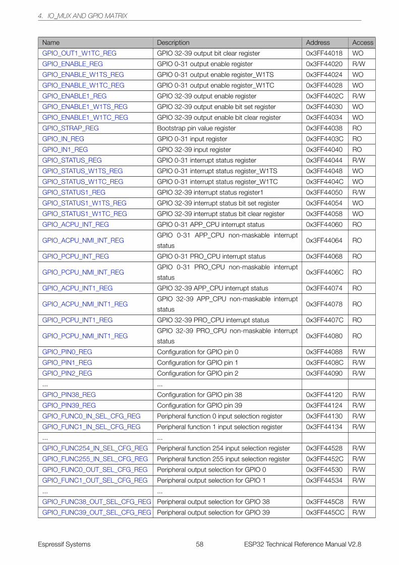
4. IO_MUX AND GPIO MATRIX
Name Description Address Access
GPIO_OUT1_W1TC_REG GPIO 32-39 output bit clear register 0x3FF44018 WO
GPIO_ENABLE_REG GPIO 0-31 output enable register 0x3FF44020 R/W
GPIO_ENABLE_W1TS_REG GPIO 0-31 output enable register_W1TS 0x3FF44024 WO
GPIO_ENABLE_W1TC_REG GPIO 0-31 output enable register_W1TC 0x3FF44028 WO
GPIO_ENABLE1_REG GPIO 32-39 output enable register 0x3FF4402C R/W
GPIO_ENABLE1_W1TS_REG GPIO 32-39 output enable bit set register 0x3FF44030 WO
GPIO_ENABLE1_W1TC_REG GPIO 32-39 output enable bit clear register 0x3FF44034 WO
GPIO_STRAP_REG Bootstrap pin value register 0x3FF44038 RO
GPIO_IN_REG GPIO 0-31 input register 0x3FF4403C RO
GPIO_IN1_REG GPIO 32-39 input register 0x3FF44040 RO
GPIO_STATUS_REG GPIO 0-31 interrupt status register 0x3FF44044 R/W
GPIO_STATUS_W1TS_REG GPIO 0-31 interrupt status register_W1TS 0x3FF44048 WO
GPIO_STATUS_W1TC_REG GPIO 0-31 interrupt status register_W1TC 0x3FF4404C WO
GPIO_STATUS1_REG GPIO 32-39 interrupt status register1 0x3FF44050 R/W
GPIO_STATUS1_W1TS_REG GPIO 32-39 interrupt status bit set register 0x3FF44054 WO
GPIO_STATUS1_W1TC_REG GPIO 32-39 interrupt status bit clear register 0x3FF44058 WO
GPIO_ACPU_INT_REG GPIO 0-31 APP_CPU interrupt status 0x3FF44060 RO
GPIO_ACPU_NMI_INT_REGGPIO 0-31 APP_CPU non-maskable interrupt
status0x3FF44064 RO
GPIO_PCPU_INT_REG GPIO 0-31 PRO_CPU interrupt status 0x3FF44068 RO
GPIO_PCPU_NMI_INT_REGGPIO 0-31 PRO_CPU non-maskable interrupt
status0x3FF4406C RO
GPIO_ACPU_INT1_REG GPIO 32-39 APP_CPU interrupt status 0x3FF44074 RO
GPIO_ACPU_NMI_INT1_REGGPIO 32-39 APP_CPU non-maskable interrupt
status0x3FF44078 RO
GPIO_PCPU_INT1_REG GPIO 32-39 PRO_CPU interrupt status 0x3FF4407C RO
GPIO_PCPU_NMI_INT1_REGGPIO 32-39 PRO_CPU non-maskable interrupt
status0x3FF44080 RO
GPIO_PIN0_REG Configuration for GPIO pin 0 0x3FF44088 R/W
GPIO_PIN1_REG Configuration for GPIO pin 1 0x3FF4408C R/W
GPIO_PIN2_REG Configuration for GPIO pin 2 0x3FF44090 R/W
... ...
GPIO_PIN38_REG Configuration for GPIO pin 38 0x3FF44120 R/W
GPIO_PIN39_REG Configuration for GPIO pin 39 0x3FF44124 R/W
GPIO_FUNC0_IN_SEL_CFG_REG Peripheral function 0 input selection register 0x3FF44130 R/W
GPIO_FUNC1_IN_SEL_CFG_REG Peripheral function 1 input selection register 0x3FF44134 R/W
... ...
GPIO_FUNC254_IN_SEL_CFG_REG Peripheral function 254 input selection register 0x3FF44528 R/W
GPIO_FUNC255_IN_SEL_CFG_REG Peripheral function 255 input selection register 0x3FF4452C R/W
GPIO_FUNC0_OUT_SEL_CFG_REG Peripheral output selection for GPIO 0 0x3FF44530 R/W
GPIO_FUNC1_OUT_SEL_CFG_REG Peripheral output selection for GPIO 1 0x3FF44534 R/W
... ...
GPIO_FUNC38_OUT_SEL_CFG_REG Peripheral output selection for GPIO 38 0x3FF445C8 R/W
GPIO_FUNC39_OUT_SEL_CFG_REG Peripheral output selection for GPIO 39 0x3FF445CC R/W
Espressif Systems 58 ESP32 Technical Reference Manual V2.8

4. IO_MUX AND GPIO MATRIX
Name Description Address Access
IO_MUX_PIN_CTRL Clock output configuration register 0x3FF49000 R/W
IO_MUX_GPIO36_REG Configuration register for pad GPIO36 0x3FF49004 R/W
IO_MUX_GPIO37_REG Configuration register for pad GPIO37 0x3FF49008 R/W
IO_MUX_GPIO38_REG Configuration register for pad GPIO38 0x3FF4900C R/W
IO_MUX_GPIO39_REG Configuration register for pad GPIO39 0x3FF49010 R/W
IO_MUX_GPIO34_REG Configuration register for pad GPIO34 0x3FF49014 R/W
IO_MUX_GPIO35_REG Configuration register for pad GPIO35 0x3FF49018 R/W
IO_MUX_GPIO32_REG Configuration register for pad GPIO32 0x3FF4901C R/W
IO_MUX_GPIO33_REG Configuration register for pad GPIO33 0x3FF49020 R/W
IO_MUX_GPIO25_REG Configuration register for pad GPIO25 0x3FF49024 R/W
IO_MUX_GPIO26_REG Configuration register for pad GPIO26 0x3FF49028 R/W
IO_MUX_GPIO27_REG Configuration register for pad GPIO27 0x3FF4902C R/W
IO_MUX_MTMS_REG Configuration register for pad MTMS 0x3FF49030 R/W
IO_MUX_MTDI_REG Configuration register for pad MTDI 0x3FF49034 R/W
IO_MUX_MTCK_REG Configuration register for pad MTCK 0x3FF49038 R/W
IO_MUX_MTDO_REG Configuration register for pad MTDO 0x3FF4903C R/W
IO_MUX_GPIO2_REG Configuration register for pad GPIO2 0x3FF49040 R/W
IO_MUX_GPIO0_REG Configuration register for pad GPIO0 0x3FF49044 R/W
IO_MUX_GPIO4_REG Configuration register for pad GPIO4 0x3FF49048 R/W
IO_MUX_GPIO16_REG Configuration register for pad GPIO16 0x3FF4904C R/W
IO_MUX_GPIO17_REG Configuration register for pad GPIO17 0x3FF49050 R/W
IO_MUX_SD_DATA2_REG Configuration register for pad SD_DATA2 0x3FF49054 R/W
IO_MUX_SD_DATA3_REG Configuration register for pad SD_DATA3 0x3FF49058 R/W
IO_MUX_SD_CMD_REG Configuration register for pad SD_CMD 0x3FF4905C R/W
IO_MUX_SD_CLK_REG Configuration register for pad SD_CLK 0x3FF49060 R/W
IO_MUX_SD_DATA0_REG Configuration register for pad SD_DATA0 0x3FF49064 R/W
IO_MUX_SD_DATA1_REG Configuration register for pad SD_DATA1 0x3FF49068 R/W
IO_MUX_GPIO5_REG Configuration register for pad GPIO5 0x3FF4906C R/W
IO_MUX_GPIO18_REG Configuration register for pad GPIO18 0x3FF49070 R/W
IO_MUX_GPIO19_REG Configuration register for pad GPIO19 0x3FF49074 R/W
IO_MUX_GPIO20_REG Configuration register for pad GPIO20 0x3FF49078 R/W
IO_MUX_GPIO21_REG Configuration register for pad GPIO21 0x3FF4907C R/W
IO_MUX_GPIO22_REG Configuration register for pad GPIO22 0x3FF49080 R/W
IO_MUX_U0RXD_REG Configuration register for pad U0RXD 0x3FF49084 R/W
IO_MUX_U0TXD_REG Configuration register for pad U0TXD 0x3FF49088 R/W
IO_MUX_GPIO23_REG Configuration register for pad GPIO23 0x3FF4908C R/W
IO_MUX_GPIO24_REG Configuration register for pad GPIO24 0x3FF49090 R/W
Name Description Address Access
GPIO configuration / data registers
RTCIO_RTC_GPIO_OUT_REG RTC GPIO output register 0x3FF48400 R/W
RTCIO_RTC_GPIO_OUT_W1TS_REG RTC GPIO output bit set register 0x3FF48404 WO
RTCIO_RTC_GPIO_OUT_W1TC_REG RTC GPIO output bit clear register 0x3FF48408 WO
RTCIO_RTC_GPIO_ENABLE_REG RTC GPIO output enable register 0x3FF4840C R/W
Espressif Systems 59 ESP32 Technical Reference Manual V2.8
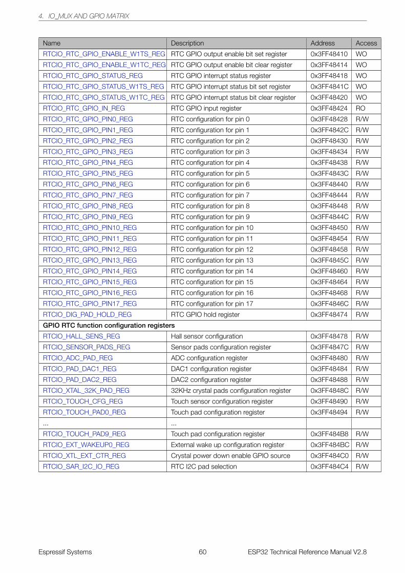
4. IO_MUX AND GPIO MATRIX
Name Description Address Access
RTCIO_RTC_GPIO_ENABLE_W1TS_REG RTC GPIO output enable bit set register 0x3FF48410 WO
RTCIO_RTC_GPIO_ENABLE_W1TC_REG RTC GPIO output enable bit clear register 0x3FF48414 WO
RTCIO_RTC_GPIO_STATUS_REG RTC GPIO interrupt status register 0x3FF48418 WO
RTCIO_RTC_GPIO_STATUS_W1TS_REG RTC GPIO interrupt status bit set register 0x3FF4841C WO
RTCIO_RTC_GPIO_STATUS_W1TC_REG RTC GPIO interrupt status bit clear register 0x3FF48420 WO
RTCIO_RTC_GPIO_IN_REG RTC GPIO input register 0x3FF48424 RO
RTCIO_RTC_GPIO_PIN0_REG RTC configuration for pin 0 0x3FF48428 R/W
RTCIO_RTC_GPIO_PIN1_REG RTC configuration for pin 1 0x3FF4842C R/W
RTCIO_RTC_GPIO_PIN2_REG RTC configuration for pin 2 0x3FF48430 R/W
RTCIO_RTC_GPIO_PIN3_REG RTC configuration for pin 3 0x3FF48434 R/W
RTCIO_RTC_GPIO_PIN4_REG RTC configuration for pin 4 0x3FF48438 R/W
RTCIO_RTC_GPIO_PIN5_REG RTC configuration for pin 5 0x3FF4843C R/W
RTCIO_RTC_GPIO_PIN6_REG RTC configuration for pin 6 0x3FF48440 R/W
RTCIO_RTC_GPIO_PIN7_REG RTC configuration for pin 7 0x3FF48444 R/W
RTCIO_RTC_GPIO_PIN8_REG RTC configuration for pin 8 0x3FF48448 R/W
RTCIO_RTC_GPIO_PIN9_REG RTC configuration for pin 9 0x3FF4844C R/W
RTCIO_RTC_GPIO_PIN10_REG RTC configuration for pin 10 0x3FF48450 R/W
RTCIO_RTC_GPIO_PIN11_REG RTC configuration for pin 11 0x3FF48454 R/W
RTCIO_RTC_GPIO_PIN12_REG RTC configuration for pin 12 0x3FF48458 R/W
RTCIO_RTC_GPIO_PIN13_REG RTC configuration for pin 13 0x3FF4845C R/W
RTCIO_RTC_GPIO_PIN14_REG RTC configuration for pin 14 0x3FF48460 R/W
RTCIO_RTC_GPIO_PIN15_REG RTC configuration for pin 15 0x3FF48464 R/W
RTCIO_RTC_GPIO_PIN16_REG RTC configuration for pin 16 0x3FF48468 R/W
RTCIO_RTC_GPIO_PIN17_REG RTC configuration for pin 17 0x3FF4846C R/W
RTCIO_DIG_PAD_HOLD_REG RTC GPIO hold register 0x3FF48474 R/W
GPIO RTC function configuration registers
RTCIO_HALL_SENS_REG Hall sensor configuration 0x3FF48478 R/W
RTCIO_SENSOR_PADS_REG Sensor pads configuration register 0x3FF4847C R/W
RTCIO_ADC_PAD_REG ADC configuration register 0x3FF48480 R/W
RTCIO_PAD_DAC1_REG DAC1 configuration register 0x3FF48484 R/W
RTCIO_PAD_DAC2_REG DAC2 configuration register 0x3FF48488 R/W
RTCIO_XTAL_32K_PAD_REG 32KHz crystal pads configuration register 0x3FF4848C R/W
RTCIO_TOUCH_CFG_REG Touch sensor configuration register 0x3FF48490 R/W
RTCIO_TOUCH_PAD0_REG Touch pad configuration register 0x3FF48494 R/W
... ...
RTCIO_TOUCH_PAD9_REG Touch pad configuration register 0x3FF484B8 R/W
RTCIO_EXT_WAKEUP0_REG External wake up configuration register 0x3FF484BC R/W
RTCIO_XTL_EXT_CTR_REG Crystal power down enable GPIO source 0x3FF484C0 R/W
RTCIO_SAR_I2C_IO_REG RTC I2C pad selection 0x3FF484C4 R/W
Espressif Systems 60 ESP32 Technical Reference Manual V2.8
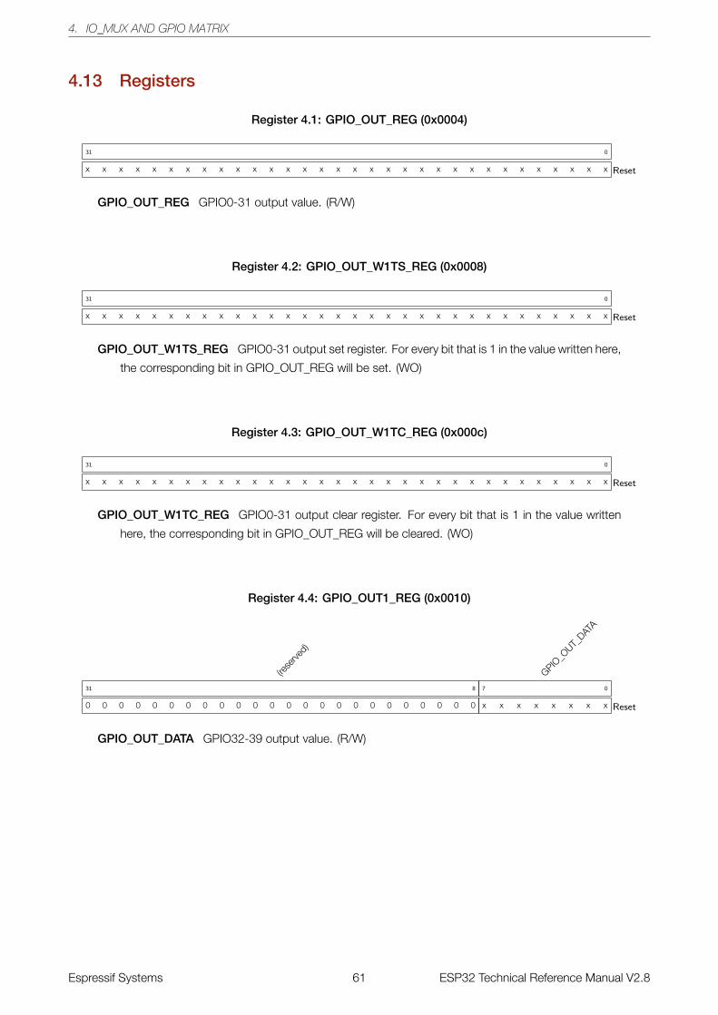
4. IO_MUX AND GPIO MATRIX
4.13 Registers
Register 4.1: GPIO_OUT_REG (0x0004)
x x x x x x x x x x x x x x x x x x x x x x x x x x x x x x x x
31 0
Reset
GPIO_OUT_REG GPIO0-31 output value. (R/W)
Register 4.2: GPIO_OUT_W1TS_REG (0x0008)
x x x x x x x x x x x x x x x x x x x x x x x x x x x x x x x x
31 0
Reset
GPIO_OUT_W1TS_REG GPIO0-31 output set register. For every bit that is 1 in the value written here,
the corresponding bit in GPIO_OUT_REG will be set. (WO)
Register 4.3: GPIO_OUT_W1TC_REG (0x000c)
x x x x x x x x x x x x x x x x x x x x x x x x x x x x x x x x
31 0
Reset
GPIO_OUT_W1TC_REG GPIO0-31 output clear register. For every bit that is 1 in the value written
here, the corresponding bit in GPIO_OUT_REG will be cleared. (WO)
Register 4.4: GPIO_OUT1_REG (0x0010)
(rese
rved)
0 0 0 0 0 0 0 0 0 0 0 0 0 0 0 0 0 0 0 0 0 0 0 0
31 8
GPIO_O
UT_DAT
A
x x x x x x x x
7 0
Reset
GPIO_OUT_DATA GPIO32-39 output value. (R/W)
Espressif Systems 61 ESP32 Technical Reference Manual V2.8
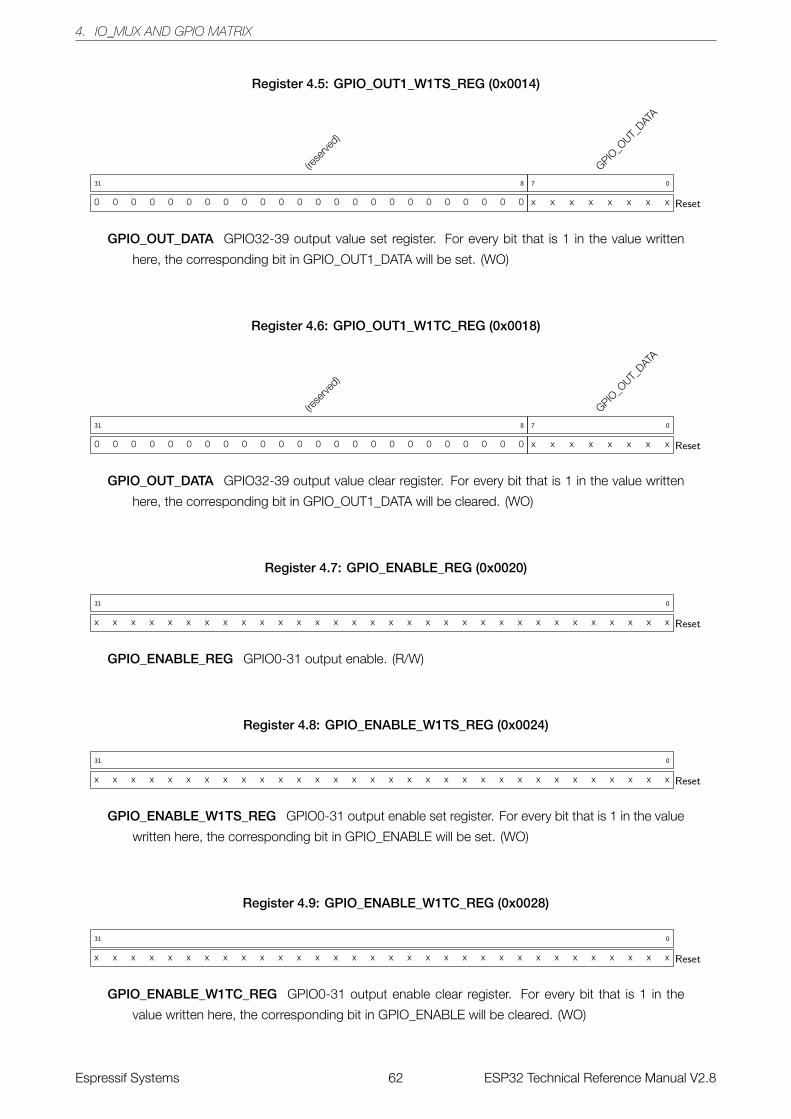
4. IO_MUX AND GPIO MATRIX
Register 4.5: GPIO_OUT1_W1TS_REG (0x0014)
(rese
rved)
0 0 0 0 0 0 0 0 0 0 0 0 0 0 0 0 0 0 0 0 0 0 0 0
31 8
GPIO_O
UT_DAT
A
x x x x x x x x
7 0
Reset
GPIO_OUT_DATA GPIO32-39 output value set register. For every bit that is 1 in the value written
here, the corresponding bit in GPIO_OUT1_DATA will be set. (WO)
Register 4.6: GPIO_OUT1_W1TC_REG (0x0018)
(rese
rved)
0 0 0 0 0 0 0 0 0 0 0 0 0 0 0 0 0 0 0 0 0 0 0 0
31 8
GPIO_O
UT_DAT
A
x x x x x x x x
7 0
Reset
GPIO_OUT_DATA GPIO32-39 output value clear register. For every bit that is 1 in the value written
here, the corresponding bit in GPIO_OUT1_DATA will be cleared. (WO)
Register 4.7: GPIO_ENABLE_REG (0x0020)
x x x x x x x x x x x x x x x x x x x x x x x x x x x x x x x x
31 0
Reset
GPIO_ENABLE_REG GPIO0-31 output enable. (R/W)
Register 4.8: GPIO_ENABLE_W1TS_REG (0x0024)
x x x x x x x x x x x x x x x x x x x x x x x x x x x x x x x x
31 0
Reset
GPIO_ENABLE_W1TS_REG GPIO0-31 output enable set register. For every bit that is 1 in the value
written here, the corresponding bit in GPIO_ENABLE will be set. (WO)
Register 4.9: GPIO_ENABLE_W1TC_REG (0x0028)
x x x x x x x x x x x x x x x x x x x x x x x x x x x x x x x x
31 0
Reset
GPIO_ENABLE_W1TC_REG GPIO0-31 output enable clear register. For every bit that is 1 in the
value written here, the corresponding bit in GPIO_ENABLE will be cleared. (WO)
Espressif Systems 62 ESP32 Technical Reference Manual V2.8
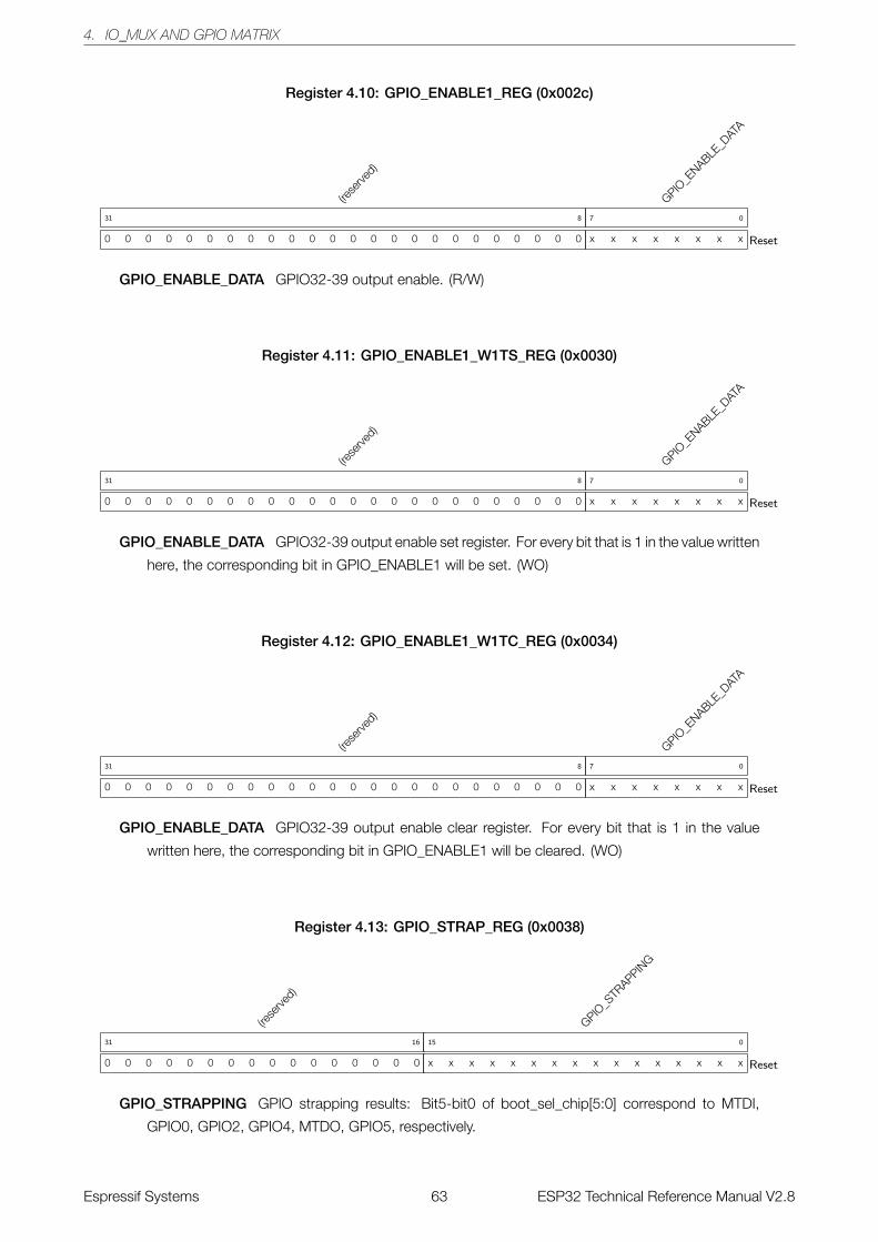
4. IO_MUX AND GPIO MATRIX
Register 4.10: GPIO_ENABLE1_REG (0x002c)
(rese
rved)
0 0 0 0 0 0 0 0 0 0 0 0 0 0 0 0 0 0 0 0 0 0 0 0
31 8
GPIO_E
NABLE_D
ATA
x x x x x x x x
7 0
Reset
GPIO_ENABLE_DATA GPIO32-39 output enable. (R/W)
Register 4.11: GPIO_ENABLE1_W1TS_REG (0x0030)
(rese
rved)
0 0 0 0 0 0 0 0 0 0 0 0 0 0 0 0 0 0 0 0 0 0 0 0
31 8
GPIO_E
NABLE_D
ATA
x x x x x x x x
7 0
Reset
GPIO_ENABLE_DATA GPIO32-39 output enable set register. For every bit that is 1 in the value written
here, the corresponding bit in GPIO_ENABLE1 will be set. (WO)
Register 4.12: GPIO_ENABLE1_W1TC_REG (0x0034)
(rese
rved)
0 0 0 0 0 0 0 0 0 0 0 0 0 0 0 0 0 0 0 0 0 0 0 0
31 8
GPIO_E
NABLE_D
ATA
x x x x x x x x
7 0
Reset
GPIO_ENABLE_DATA GPIO32-39 output enable clear register. For every bit that is 1 in the value
written here, the corresponding bit in GPIO_ENABLE1 will be cleared. (WO)
Register 4.13: GPIO_STRAP_REG (0x0038)
(rese
rved)
0 0 0 0 0 0 0 0 0 0 0 0 0 0 0 0
31 16
GPIO_S
TRAPPIN
G
x x x x x x x x x x x x x x x x
15 0
Reset
GPIO_STRAPPING GPIO strapping results: Bit5-bit0 of boot_sel_chip[5:0] correspond to MTDI,
GPIO0, GPIO2, GPIO4, MTDO, GPIO5, respectively.
Espressif Systems 63 ESP32 Technical Reference Manual V2.8
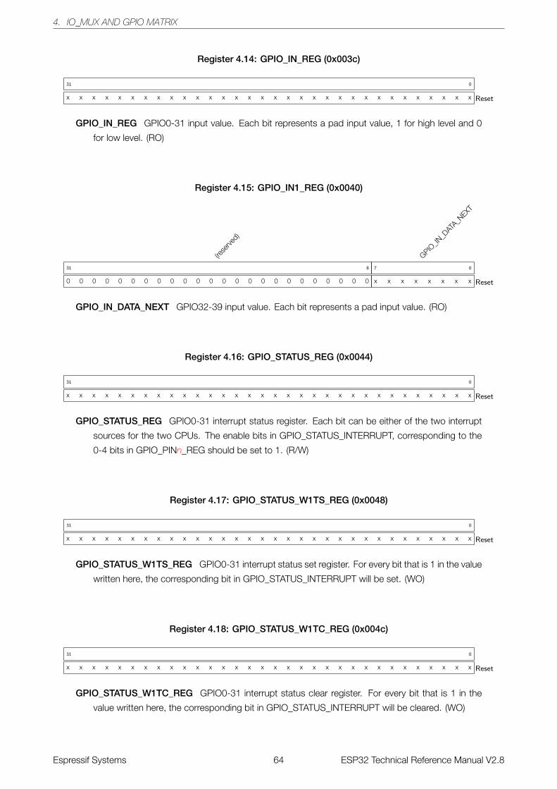
4. IO_MUX AND GPIO MATRIX
Register 4.14: GPIO_IN_REG (0x003c)
x x x x x x x x x x x x x x x x x x x x x x x x x x x x x x x x
31 0
Reset
GPIO_IN_REG GPIO0-31 input value. Each bit represents a pad input value, 1 for high level and 0
for low level. (RO)
Register 4.15: GPIO_IN1_REG (0x0040)
(rese
rved)
0 0 0 0 0 0 0 0 0 0 0 0 0 0 0 0 0 0 0 0 0 0 0 0
31 8
GPIO_IN
_DAT
A_NEXT
x x x x x x x x
7 0
Reset
GPIO_IN_DATA_NEXT GPIO32-39 input value. Each bit represents a pad input value. (RO)
Register 4.16: GPIO_STATUS_REG (0x0044)
x x x x x x x x x x x x x x x x x x x x x x x x x x x x x x x x
31 0
Reset
GPIO_STATUS_REG GPIO0-31 interrupt status register. Each bit can be either of the two interrupt
sources for the two CPUs. The enable bits in GPIO_STATUS_INTERRUPT, corresponding to the
0-4 bits in GPIO_PINn_REG should be set to 1. (R/W)
Register 4.17: GPIO_STATUS_W1TS_REG (0x0048)
x x x x x x x x x x x x x x x x x x x x x x x x x x x x x x x x
31 0
Reset
GPIO_STATUS_W1TS_REG GPIO0-31 interrupt status set register. For every bit that is 1 in the value
written here, the corresponding bit in GPIO_STATUS_INTERRUPT will be set. (WO)
Register 4.18: GPIO_STATUS_W1TC_REG (0x004c)
x x x x x x x x x x x x x x x x x x x x x x x x x x x x x x x x
31 0
Reset
GPIO_STATUS_W1TC_REG GPIO0-31 interrupt status clear register. For every bit that is 1 in the
value written here, the corresponding bit in GPIO_STATUS_INTERRUPT will be cleared. (WO)
Espressif Systems 64 ESP32 Technical Reference Manual V2.8
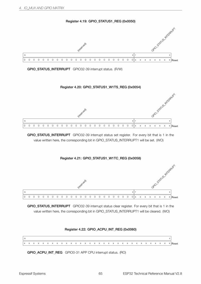
4. IO_MUX AND GPIO MATRIX
Register 4.19: GPIO_STATUS1_REG (0x0050)
(rese
rved)
0 0 0 0 0 0 0 0 0 0 0 0 0 0 0 0 0 0 0 0 0 0 0 0
31 8
GPIO_S
TATU
S_INTE
RRUPT
x x x x x x x x
7 0
Reset
GPIO_STATUS_INTERRUPT GPIO32-39 interrupt status. (R/W)
Register 4.20: GPIO_STATUS1_W1TS_REG (0x0054)
(rese
rved)
0 0 0 0 0 0 0 0 0 0 0 0 0 0 0 0 0 0 0 0 0 0 0 0
31 8
GPIO_S
TATU
S_INTE
RRUPT
x x x x x x x x
7 0
Reset
GPIO_STATUS_INTERRUPT GPIO32-39 interrupt status set register. For every bit that is 1 in the
value written here, the corresponding bit in GPIO_STATUS_INTERRUPT1 will be set. (WO)
Register 4.21: GPIO_STATUS1_W1TC_REG (0x0058)
(rese
rved)
0 0 0 0 0 0 0 0 0 0 0 0 0 0 0 0 0 0 0 0 0 0 0 0
31 8
GPIO_S
TATU
S_INTE
RRUPT
x x x x x x x x
7 0
Reset
GPIO_STATUS_INTERRUPT GPIO32-39 interrupt status clear register. For every bit that is 1 in the
value written here, the corresponding bit in GPIO_STATUS_INTERRUPT1 will be cleared. (WO)
Register 4.22: GPIO_ACPU_INT_REG (0x0060)
x x x x x x x x x x x x x x x x x x x x x x x x x x x x x x x x
31 0
Reset
GPIO_ACPU_INT_REG GPIO0-31 APP CPU interrupt status. (RO)
Espressif Systems 65 ESP32 Technical Reference Manual V2.8
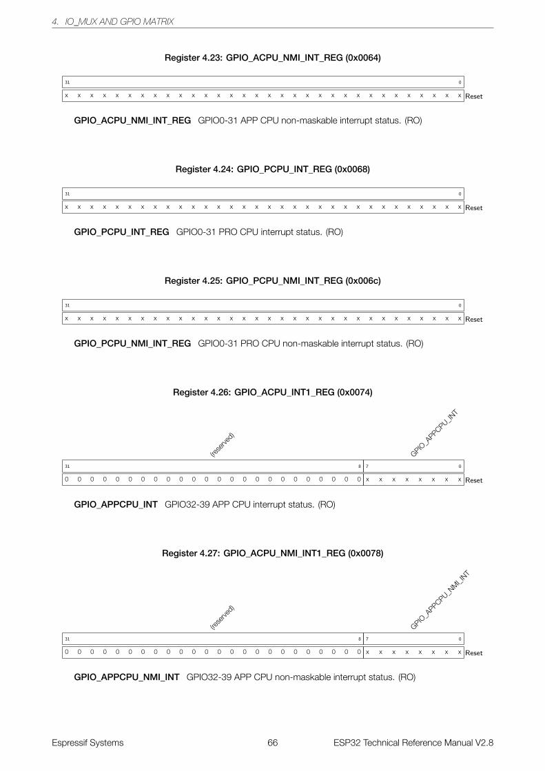
4. IO_MUX AND GPIO MATRIX
Register 4.23: GPIO_ACPU_NMI_INT_REG (0x0064)
x x x x x x x x x x x x x x x x x x x x x x x x x x x x x x x x
31 0
Reset
GPIO_ACPU_NMI_INT_REG GPIO0-31 APP CPU non-maskable interrupt status. (RO)
Register 4.24: GPIO_PCPU_INT_REG (0x0068)
x x x x x x x x x x x x x x x x x x x x x x x x x x x x x x x x
31 0
Reset
GPIO_PCPU_INT_REG GPIO0-31 PRO CPU interrupt status. (RO)
Register 4.25: GPIO_PCPU_NMI_INT_REG (0x006c)
x x x x x x x x x x x x x x x x x x x x x x x x x x x x x x x x
31 0
Reset
GPIO_PCPU_NMI_INT_REG GPIO0-31 PRO CPU non-maskable interrupt status. (RO)
Register 4.26: GPIO_ACPU_INT1_REG (0x0074)
(rese
rved)
0 0 0 0 0 0 0 0 0 0 0 0 0 0 0 0 0 0 0 0 0 0 0 0
31 8
GPIO_A
PPCPU_INT
x x x x x x x x
7 0
Reset
GPIO_APPCPU_INT GPIO32-39 APP CPU interrupt status. (RO)
Register 4.27: GPIO_ACPU_NMI_INT1_REG (0x0078)
(rese
rved)
0 0 0 0 0 0 0 0 0 0 0 0 0 0 0 0 0 0 0 0 0 0 0 0
31 8
GPIO_A
PPCPU_NM
I_INT
x x x x x x x x
7 0
Reset
GPIO_APPCPU_NMI_INT GPIO32-39 APP CPU non-maskable interrupt status. (RO)
Espressif Systems 66 ESP32 Technical Reference Manual V2.8
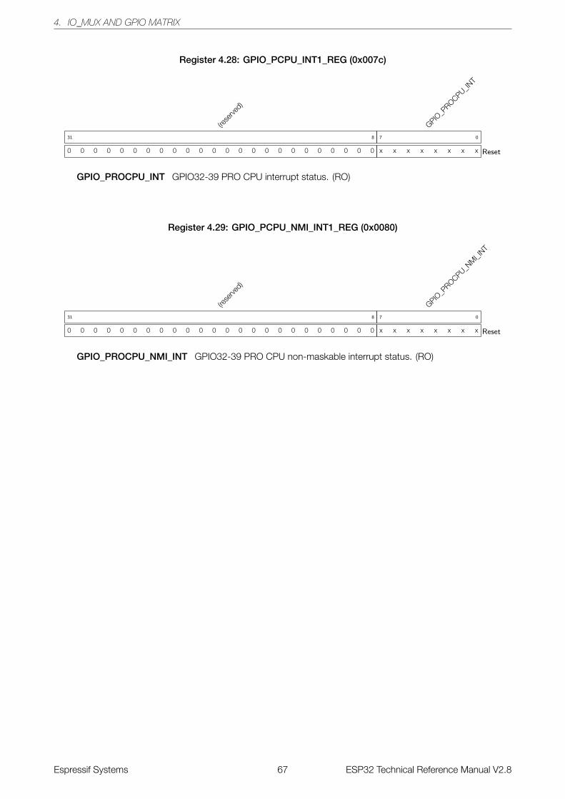
4. IO_MUX AND GPIO MATRIX
Register 4.28: GPIO_PCPU_INT1_REG (0x007c)
(rese
rved)
0 0 0 0 0 0 0 0 0 0 0 0 0 0 0 0 0 0 0 0 0 0 0 0
31 8
GPIO_P
ROCPU_INT
x x x x x x x x
7 0
Reset
GPIO_PROCPU_INT GPIO32-39 PRO CPU interrupt status. (RO)
Register 4.29: GPIO_PCPU_NMI_INT1_REG (0x0080)
(rese
rved)
0 0 0 0 0 0 0 0 0 0 0 0 0 0 0 0 0 0 0 0 0 0 0 0
31 8
GPIO_P
ROCPU_NM
I_INT
x x x x x x x x
7 0
Reset
GPIO_PROCPU_NMI_INT GPIO32-39 PRO CPU non-maskable interrupt status. (RO)
Espressif Systems 67 ESP32 Technical Reference Manual V2.8
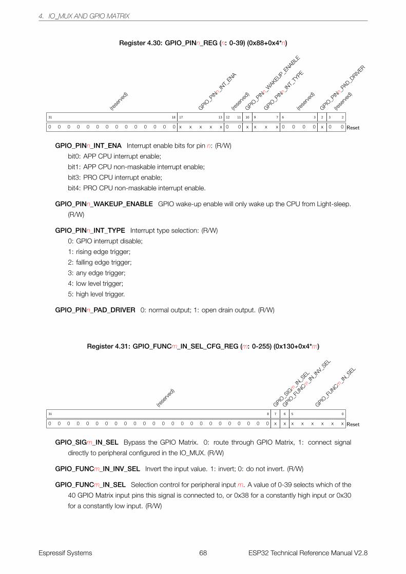
4. IO_MUX AND GPIO MATRIX
Register 4.30: GPIO_PINn_REG (n: 0-39) (0x88+0x4*n)
(rese
rved)
0 0 0 0 0 0 0 0 0 0 0 0 0 0
31 18
GPIO_P
INn_
INT_
ENA
x x x x x
17 13
(rese
rved)
0 0
12 11
GPIO_P
INn_
WAKEUP_E
NABLE
x
10
GPIO_P
INn_
INT_
TYPE
x x x
9 7
(rese
rved)
0 0 0 0
6 3
GPIO_P
INn_
PAD_D
RIVER
x
2
(rese
rved)
0 0
3 2
Reset
GPIO_PINn_INT_ENA Interrupt enable bits for pin n: (R/W)
bit0: APP CPU interrupt enable;
bit1: APP CPU non-maskable interrupt enable;
bit3: PRO CPU interrupt enable;
bit4: PRO CPU non-maskable interrupt enable.
GPIO_PINn_WAKEUP_ENABLE GPIO wake-up enable will only wake up the CPU from Light-sleep.
(R/W)
GPIO_PINn_INT_TYPE Interrupt type selection: (R/W)
0: GPIO interrupt disable;
1: rising edge trigger;
2: falling edge trigger;
3: any edge trigger;
4: low level trigger;
5: high level trigger.
GPIO_PINn_PAD_DRIVER 0: normal output; 1: open drain output. (R/W)
Register 4.31: GPIO_FUNCm_IN_SEL_CFG_REG (m: 0-255) (0x130+0x4*m)
(rese
rved)
0 0 0 0 0 0 0 0 0 0 0 0 0 0 0 0 0 0 0 0 0 0 0 0
31 8
GPIO_S
IGm_IN
_SEL
x
7
GPIO_F
UNCm_IN
_INV_S
EL
x
6
GPIO_F
UNCm_IN
_SEL
x x x x x x
5 0
Reset
GPIO_SIGm_IN_SEL Bypass the GPIO Matrix. 0: route through GPIO Matrix, 1: connect signal
directly to peripheral configured in the IO_MUX. (R/W)
GPIO_FUNCm_IN_INV_SEL Invert the input value. 1: invert; 0: do not invert. (R/W)
GPIO_FUNCm_IN_SEL Selection control for peripheral input m. A value of 0-39 selects which of the
40 GPIO Matrix input pins this signal is connected to, or 0x38 for a constantly high input or 0x30
for a constantly low input. (R/W)
Espressif Systems 68 ESP32 Technical Reference Manual V2.8
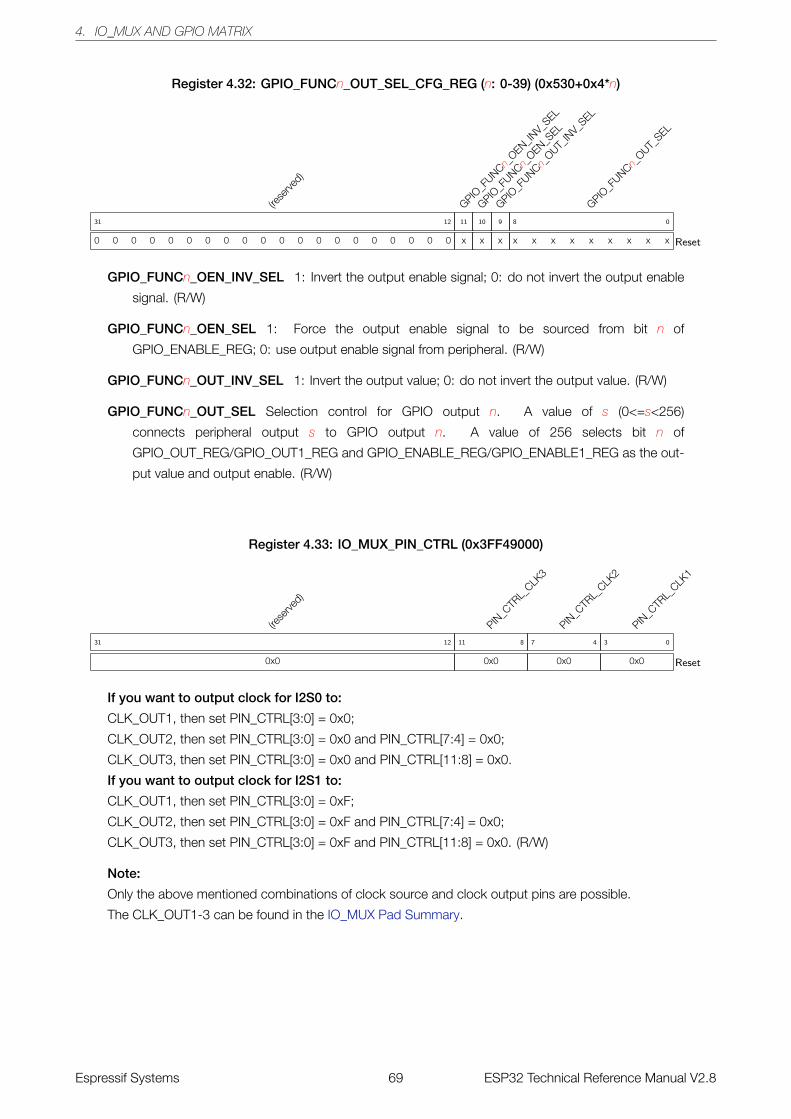
4. IO_MUX AND GPIO MATRIX
Register 4.32: GPIO_FUNCn_OUT_SEL_CFG_REG (n: 0-39) (0x530+0x4*n)
(rese
rved)
0 0 0 0 0 0 0 0 0 0 0 0 0 0 0 0 0 0 0 0
31 12
GPIO_F
UNCn_O
EN_INV_S
EL
x
11
GPIO_F
UNCn_O
EN_SEL
x
10
GPIO_F
UNCn_O
UT_IN
V_SEL
x
9
GPIO_F
UNCn_O
UT_SEL
x x x x x x x x x
8 0
Reset
GPIO_FUNCn_OEN_INV_SEL 1: Invert the output enable signal; 0: do not invert the output enable
signal. (R/W)
GPIO_FUNCn_OEN_SEL 1: Force the output enable signal to be sourced from bit n of
GPIO_ENABLE_REG; 0: use output enable signal from peripheral. (R/W)
GPIO_FUNCn_OUT_INV_SEL 1: Invert the output value; 0: do not invert the output value. (R/W)
GPIO_FUNCn_OUT_SEL Selection control for GPIO output n. A value of s (0<=s<256)
connects peripheral output s to GPIO output n. A value of 256 selects bit n of
GPIO_OUT_REG/GPIO_OUT1_REG and GPIO_ENABLE_REG/GPIO_ENABLE1_REG as the out-
put value and output enable. (R/W)
Register 4.33: IO_MUX_PIN_CTRL (0x3FF49000)
(rese
rved)
0x0
31 12
PIN_C
TRL_
CLK3
0x0
11 8
PIN_C
TRL_
CLK2
0x0
7 4
PIN_C
TRL_
CLK1
0x0
3 0
Reset
If you want to output clock for I2S0 to:
CLK_OUT1, then set PIN_CTRL[3:0] = 0x0;
CLK_OUT2, then set PIN_CTRL[3:0] = 0x0 and PIN_CTRL[7:4] = 0x0;
CLK_OUT3, then set PIN_CTRL[3:0] = 0x0 and PIN_CTRL[11:8] = 0x0.
If you want to output clock for I2S1 to:
CLK_OUT1, then set PIN_CTRL[3:0] = 0xF;
CLK_OUT2, then set PIN_CTRL[3:0] = 0xF and PIN_CTRL[7:4] = 0x0;
CLK_OUT3, then set PIN_CTRL[3:0] = 0xF and PIN_CTRL[11:8] = 0x0. (R/W)
Note:
Only the above mentioned combinations of clock source and clock output pins are possible.
The CLK_OUT1-3 can be found in the IO_MUX Pad Summary.
Espressif Systems 69 ESP32 Technical Reference Manual V2.8
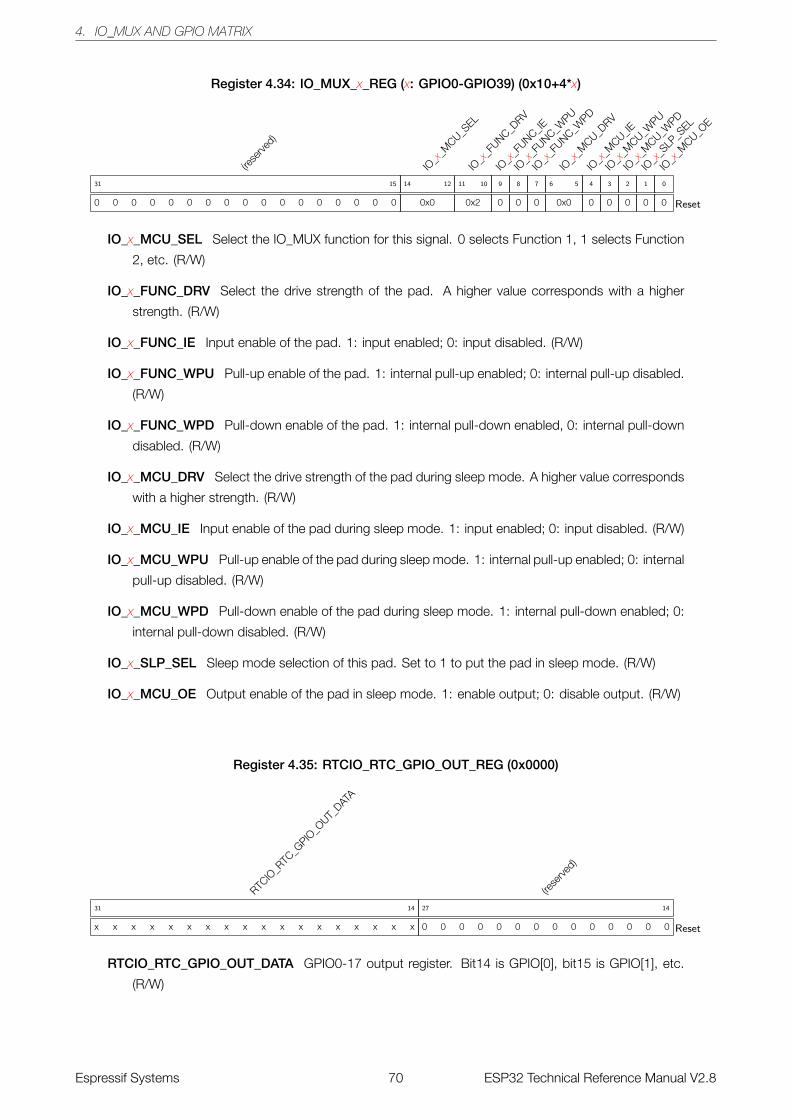
4. IO_MUX AND GPIO MATRIX
Register 4.34: IO_MUX_x_REG (x: GPIO0-GPIO39) (0x10+4*x)
(rese
rved)
0 0 0 0 0 0 0 0 0 0 0 0 0 0 0 0 0
31 15
IO_x
_MCU_S
EL
0x0
14 12
IO_x
_FUNC_D
RV
0x2
11 10
IO_x
_FUNC_IE
0
9
IO_x
_FUNC_W
PU
0
8
IO_x
_FUNC_W
PD
0
7
IO_x
_MCU_D
RV
0x0
6 5
IO_x
_MCU_IE
0
4
IO_x
_MCU_W
PU
0
3
IO_x
_MCU_W
PD
0
2
IO_x
_SLP
_SEL
0
1
IO_x
_MCU_O
E
0
0
Reset
IO_x_MCU_SEL Select the IO_MUX function for this signal. 0 selects Function 1, 1 selects Function
2, etc. (R/W)
IO_x_FUNC_DRV Select the drive strength of the pad. A higher value corresponds with a higher
strength. (R/W)
IO_x_FUNC_IE Input enable of the pad. 1: input enabled; 0: input disabled. (R/W)
IO_x_FUNC_WPU Pull-up enable of the pad. 1: internal pull-up enabled; 0: internal pull-up disabled.
(R/W)
IO_x_FUNC_WPD Pull-down enable of the pad. 1: internal pull-down enabled, 0: internal pull-down
disabled. (R/W)
IO_x_MCU_DRV Select the drive strength of the pad during sleep mode. A higher value corresponds
with a higher strength. (R/W)
IO_x_MCU_IE Input enable of the pad during sleep mode. 1: input enabled; 0: input disabled. (R/W)
IO_x_MCU_WPU Pull-up enable of the pad during sleep mode. 1: internal pull-up enabled; 0: internal
pull-up disabled. (R/W)
IO_x_MCU_WPD Pull-down enable of the pad during sleep mode. 1: internal pull-down enabled; 0:
internal pull-down disabled. (R/W)
IO_x_SLP_SEL Sleep mode selection of this pad. Set to 1 to put the pad in sleep mode. (R/W)
IO_x_MCU_OE Output enable of the pad in sleep mode. 1: enable output; 0: disable output. (R/W)
Register 4.35: RTCIO_RTC_GPIO_OUT_REG (0x0000)
RTCIO
_RTC
_GPIO
_OUT_
DATA
x x x x x x x x x x x x x x x x x x
31 14
(rese
rved)
0 0 0 0 0 0 0 0 0 0 0 0 0 0
27 14
Reset
RTCIO_RTC_GPIO_OUT_DATA GPIO0-17 output register. Bit14 is GPIO[0], bit15 is GPIO[1], etc.
(R/W)
Espressif Systems 70 ESP32 Technical Reference Manual V2.8
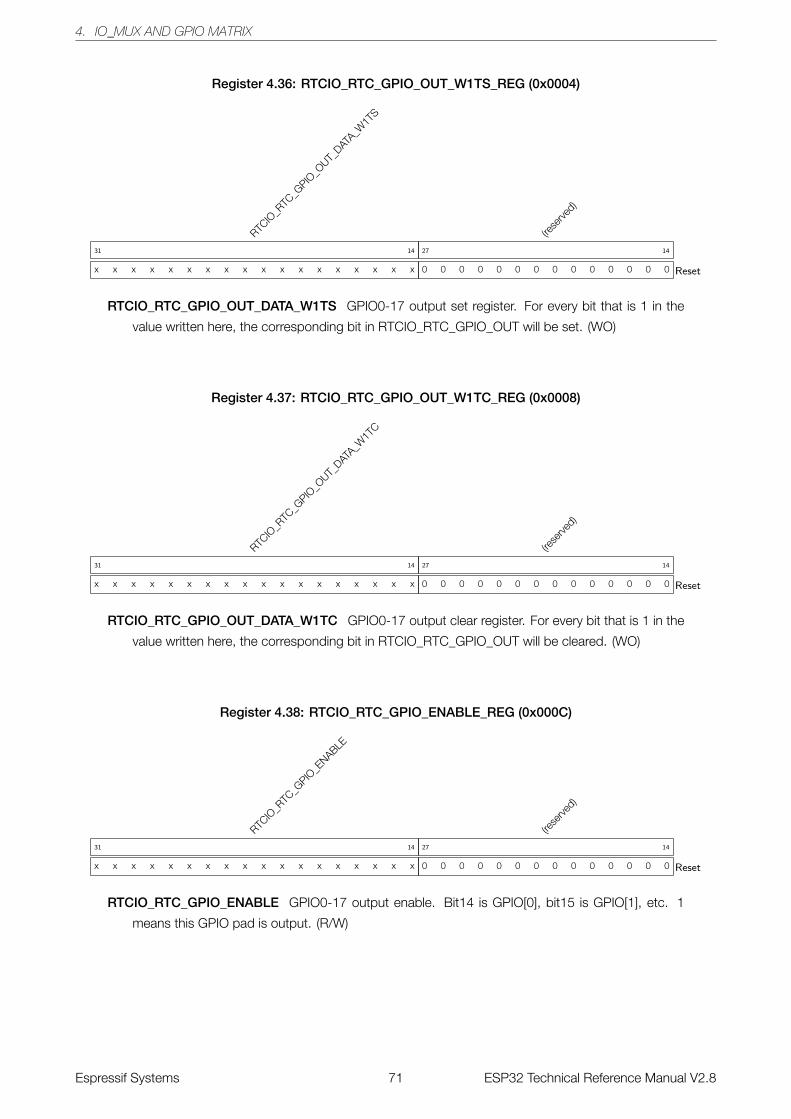
4. IO_MUX AND GPIO MATRIX
Register 4.36: RTCIO_RTC_GPIO_OUT_W1TS_REG (0x0004)
RTCIO
_RTC
_GPIO
_OUT_
DATA_W
1TS
x x x x x x x x x x x x x x x x x x
31 14
(rese
rved)
0 0 0 0 0 0 0 0 0 0 0 0 0 0
27 14
Reset
RTCIO_RTC_GPIO_OUT_DATA_W1TS GPIO0-17 output set register. For every bit that is 1 in the
value written here, the corresponding bit in RTCIO_RTC_GPIO_OUT will be set. (WO)
Register 4.37: RTCIO_RTC_GPIO_OUT_W1TC_REG (0x0008)
RTCIO
_RTC
_GPIO
_OUT_
DATA_W
1TC
x x x x x x x x x x x x x x x x x x
31 14
(rese
rved)
0 0 0 0 0 0 0 0 0 0 0 0 0 0
27 14
Reset
RTCIO_RTC_GPIO_OUT_DATA_W1TC GPIO0-17 output clear register. For every bit that is 1 in the
value written here, the corresponding bit in RTCIO_RTC_GPIO_OUT will be cleared. (WO)
Register 4.38: RTCIO_RTC_GPIO_ENABLE_REG (0x000C)
RTCIO
_RTC
_GPIO
_ENABLE
x x x x x x x x x x x x x x x x x x
31 14
(rese
rved)
0 0 0 0 0 0 0 0 0 0 0 0 0 0
27 14
Reset
RTCIO_RTC_GPIO_ENABLE GPIO0-17 output enable. Bit14 is GPIO[0], bit15 is GPIO[1], etc. 1
means this GPIO pad is output. (R/W)
Espressif Systems 71 ESP32 Technical Reference Manual V2.8
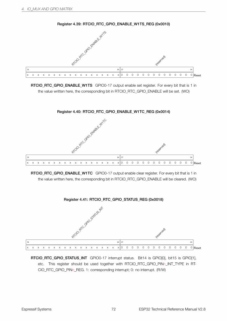
4. IO_MUX AND GPIO MATRIX
Register 4.39: RTCIO_RTC_GPIO_ENABLE_W1TS_REG (0x0010)
RTCIO
_RTC
_GPIO
_ENABLE
_W1T
S
x x x x x x x x x x x x x x x x x x
31 14
(rese
rved)
0 0 0 0 0 0 0 0 0 0 0 0 0 0
27 14
Reset
RTCIO_RTC_GPIO_ENABLE_W1TS GPIO0-17 output enable set register. For every bit that is 1 in
the value written here, the corresponding bit in RTCIO_RTC_GPIO_ENABLE will be set. (WO)
Register 4.40: RTCIO_RTC_GPIO_ENABLE_W1TC_REG (0x0014)
RTCIO
_RTC
_GPIO
_ENABLE
_W1T
C
x x x x x x x x x x x x x x x x x x
31 14
(rese
rved)
0 0 0 0 0 0 0 0 0 0 0 0 0 0
27 14
Reset
RTCIO_RTC_GPIO_ENABLE_W1TC GPIO0-17 output enable clear register. For every bit that is 1 in
the value written here, the corresponding bit in RTCIO_RTC_GPIO_ENABLE will be cleared. (WO)
Register 4.41: RTCIO_RTC_GPIO_STATUS_REG (0x0018)
RTCIO
_RTC
_GPIO
_STA
TUS_IN
T
x x x x x x x x x x x x x x x x x x
31 14
(rese
rved)
0 0 0 0 0 0 0 0 0 0 0 0 0 0
27 14
Reset
RTCIO_RTC_GPIO_STATUS_INT GPIO0-17 interrupt status. Bit14 is GPIO[0], bit15 is GPIO[1],
etc. This register should be used together with RTCIO_RTC_GPIO_PINn_INT_TYPE in RT-
CIO_RTC_GPIO_PINn_REG. 1: corresponding interrupt; 0: no interrupt. (R/W)
Espressif Systems 72 ESP32 Technical Reference Manual V2.8
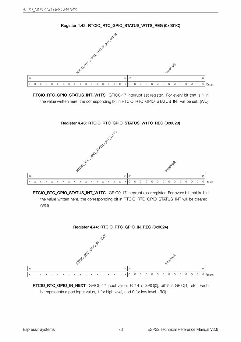
4. IO_MUX AND GPIO MATRIX
Register 4.42: RTCIO_RTC_GPIO_STATUS_W1TS_REG (0x001C)
RTCIO
_RTC
_GPIO
_STA
TUS_IN
T_W
1TS
x x x x x x x x x x x x x x x x x x
31 14
(rese
rved)
0 0 0 0 0 0 0 0 0 0 0 0 0 0
27 14
Reset
RTCIO_RTC_GPIO_STATUS_INT_W1TS GPIO0-17 interrupt set register. For every bit that is 1 in
the value written here, the corresponding bit in RTCIO_RTC_GPIO_STATUS_INT will be set. (WO)
Register 4.43: RTCIO_RTC_GPIO_STATUS_W1TC_REG (0x0020)
RTCIO
_RTC
_GPIO
_STA
TUS_IN
T_W
1TC
x x x x x x x x x x x x x x x x x x
31 14
(rese
rved)
0 0 0 0 0 0 0 0 0 0 0 0 0 0
27 14
Reset
RTCIO_RTC_GPIO_STATUS_INT_W1TC GPIO0-17 interrupt clear register. For every bit that is 1 in
the value written here, the corresponding bit in RTCIO_RTC_GPIO_STATUS_INT will be cleared.
(WO)
Register 4.44: RTCIO_RTC_GPIO_IN_REG (0x0024)
RTCIO
_RTC
_GPIO
_IN_N
EXT
x x x x x x x x x x x x x x x x x x
31 14
(rese
rved)
0 0 0 0 0 0 0 0 0 0 0 0 0 0
27 14
Reset
RTCIO_RTC_GPIO_IN_NEXT GPIO0-17 input value. Bit14 is GPIO[0], bit15 is GPIO[1], etc. Each
bit represents a pad input value, 1 for high level, and 0 for low level. (RO)
Espressif Systems 73 ESP32 Technical Reference Manual V2.8
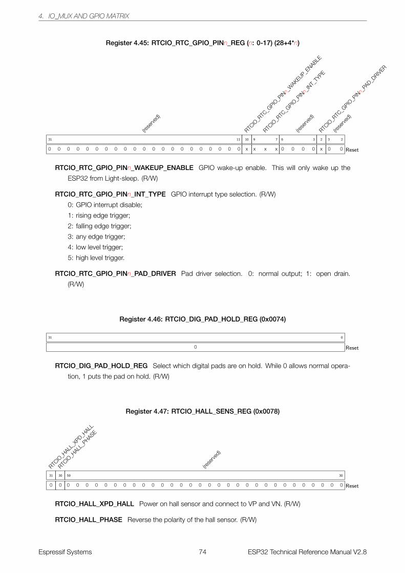
4. IO_MUX AND GPIO MATRIX
Register 4.45: RTCIO_RTC_GPIO_PINn_REG (n: 0-17) (28+4*n)
(rese
rved)
0 0 0 0 0 0 0 0 0 0 0 0 0 0 0 0 0 0 0 0 0
31 11
RTCIO
_RTC
_GPIO
_PINn_
WAKEUP_E
NABLE
x
10
RTCIO
_RTC
_GPIO
_PINn_
INT_
TYPE
x x x
9 7
(rese
rved)
0 0 0 0
6 3
RTCIO
_RTC
_GPIO
_PINn_
PAD_D
RIVER
x
2
(rese
rved)
0 0
3 2
Reset
RTCIO_RTC_GPIO_PINn_WAKEUP_ENABLE GPIO wake-up enable. This will only wake up the
ESP32 from Light-sleep. (R/W)
RTCIO_RTC_GPIO_PINn_INT_TYPE GPIO interrupt type selection. (R/W)
0: GPIO interrupt disable;
1: rising edge trigger;
2: falling edge trigger;
3: any edge trigger;
4: low level trigger;
5: high level trigger.
RTCIO_RTC_GPIO_PINn_PAD_DRIVER Pad driver selection. 0: normal output; 1: open drain.
(R/W)
Register 4.46: RTCIO_DIG_PAD_HOLD_REG (0x0074)
0
31 0
Reset
RTCIO_DIG_PAD_HOLD_REG Select which digital pads are on hold. While 0 allows normal opera-
tion, 1 puts the pad on hold. (R/W)
Register 4.47: RTCIO_HALL_SENS_REG (0x0078)
RTCIO
_HALL
_XPD_H
ALL
0
31
RTCIO
_HALL
_PHASE
0
30
(rese
rved)
0 0 0 0 0 0 0 0 0 0 0 0 0 0 0 0 0 0 0 0 0 0 0 0 0 0 0 0 0 0
59 30
Reset
RTCIO_HALL_XPD_HALL Power on hall sensor and connect to VP and VN. (R/W)
RTCIO_HALL_PHASE Reverse the polarity of the hall sensor. (R/W)
Espressif Systems 74 ESP32 Technical Reference Manual V2.8
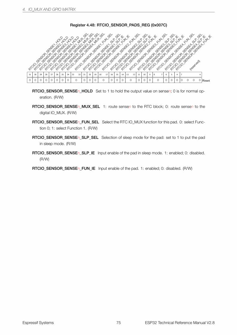
4. IO_MUX AND GPIO MATRIX
Register 4.48: RTCIO_SENSOR_PADS_REG (0x007C)
RTCIO
_SENSOR_S
ENSE1_HOLD
0
31
RTCIO
_SENSOR_S
ENSE2_HOLD
0
30
RTCIO
_SENSOR_S
ENSE3_HOLD
0
29
RTCIO
_SENSOR_S
ENSE4_HOLD
0
28
RTCIO
_SENSOR_S
ENSE1_M
UX_SEL
0
27
RTCIO
_SENSOR_S
ENSE2_M
UX_SEL
0
26
RTCIO
_SENSOR_S
ENSE3_M
UX_SEL
0
25
RTCIO
_SENSOR_S
ENSE4_M
UX_SEL
0
24
RTCIO
_SENSOR_S
ENSE1_FU
N_SEL
0
23 22
RTCIO
_SENSOR_S
ENSE1_SLP
_SEL
0
21
RTCIO
_SENSOR_S
ENSE1_SLP
_IE
0
20
RTCIO
_SENSOR_S
ENSE1_FU
N_IE
0
19
RTCIO
_SENSOR_S
ENSE2_FU
N_SEL
0
18 17
RTCIO
_SENSOR_S
ENSE2_SLP
_SEL
0
16
RTCIO
_SENSOR_S
ENSE2_SLP
_IE
0
15
RTCIO
_SENSOR_S
ENSE2_FU
N_IE
0
14
RTCIO
_SENSOR_S
ENSE3_FU
N_SEL
0
13 12
RTCIO
_SENSOR_S
ENSE3_SLP
_SEL
0
11
RTCIO
_SENSOR_S
ENSE3_SLP
_IE
0
10
RTCIO
_SENSOR_S
ENSE3_FU
N_IE
0
9
RTCIO
_SENSOR_S
ENSE4_FU
N_SEL
0
8 7
RTCIO
_SENSOR_S
ENSE4_SLP
_SEL
0
6
RTCIO
_SENSOR_S
ENSE4_SLP
_IE
0
5
RTCIO
_SENSOR_S
ENSE4_FU
N_IE
0
4
(rese
rved)
0 0 0 0
7 4
Reset
RTCIO_SENSOR_SENSEn_HOLD Set to 1 to hold the output value on sensen; 0 is for normal op-
eration. (R/W)
RTCIO_SENSOR_SENSEn_MUX_SEL 1: route sensen to the RTC block; 0: route sensen to the
digital IO_MUX. (R/W)
RTCIO_SENSOR_SENSEn_FUN_SEL Select the RTC IO_MUX function for this pad. 0: select Func-
tion 0; 1: select Function 1. (R/W)
RTCIO_SENSOR_SENSEn_SLP_SEL Selection of sleep mode for the pad: set to 1 to put the pad
in sleep mode. (R/W)
RTCIO_SENSOR_SENSEn_SLP_IE Input enable of the pad in sleep mode. 1: enabled; 0: disabled.
(R/W)
RTCIO_SENSOR_SENSEn_FUN_IE Input enable of the pad. 1: enabled; 0: disabled. (R/W)
Espressif Systems 75 ESP32 Technical Reference Manual V2.8
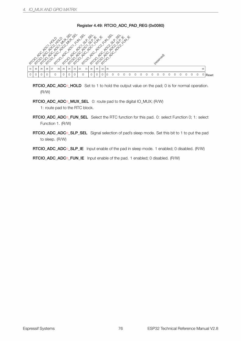
4. IO_MUX AND GPIO MATRIX
Register 4.49: RTCIO_ADC_PAD_REG (0x0080)
RTCIO
_ADC_A
DC1_HOLD
0
31
RTCIO
_ADC_A
DC2_HOLD
0
30
RTCIO
_ADC_A
DC1_M
UX_SEL
0
29
RTCIO
_ADC_A
DC2_M
UX_SEL
0
28
RTCIO
_ADC_A
DC1_FU
N_SEL
0
27 26
RTCIO
_ADC_A
DC1_SLP
_SEL
0
25
RTCIO
_ADC_A
DC1_SLP
_IE
0
24
RTCIO
_ADC_A
DC1_FU
N_IE
0
23
RTCIO
_ADC_A
DC2_FU
N_SEL
0
22 21
RTCIO
_ADC_A
DC2_SLP
_SEL
0
20
RTCIO
_ADC_A
DC2_SLP
_IE
0
19
RTCIO
_ADC_A
DC2_FU
N_IE
0
18
(rese
rved)
0 0 0 0 0 0 0 0 0 0 0 0 0 0 0 0 0 0
35 18
Reset
RTCIO_ADC_ADCn_HOLD Set to 1 to hold the output value on the pad; 0 is for normal operation.
(R/W)
RTCIO_ADC_ADCn_MUX_SEL 0: route pad to the digital IO_MUX; (R/W)
1: route pad to the RTC block.
RTCIO_ADC_ADCn_FUN_SEL Select the RTC function for this pad. 0: select Function 0; 1: select
Function 1. (R/W)
RTCIO_ADC_ADCn_SLP_SEL Signal selection of pad’s sleep mode. Set this bit to 1 to put the pad
to sleep. (R/W)
RTCIO_ADC_ADCn_SLP_IE Input enable of the pad in sleep mode. 1 enabled; 0 disabled. (R/W)
RTCIO_ADC_ADCn_FUN_IE Input enable of the pad. 1 enabled; 0 disabled. (R/W)
Espressif Systems 76 ESP32 Technical Reference Manual V2.8
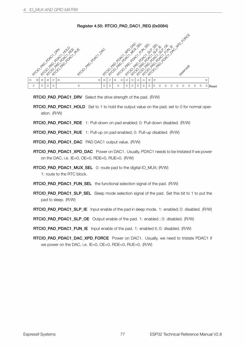
4. IO_MUX AND GPIO MATRIX
Register 4.50: RTCIO_PAD_DAC1_REG (0x0084)
RTCIO
_PAD_P
DAC1_DRV
2
31 30
RTCIO
_PAD_P
DAC1_HOLD
0
29
RTCIO
_PAD_P
DAC1_RDE
0
28
RTCIO
_PAD_P
DAC1_RUE
0
27
RTCIO
_PAD_P
DAC1_DAC
0
26 19
RTCIO
_PAD_P
DAC1_XP
D_DAC
0
18
RTCIO
_PAD_P
DAC1_M
UX_SEL
0
17
RTCIO
_PAD_P
DAC1_FU
N_SEL
0
16 15
RTCIO
_PAD_P
DAC1_SLP
_SEL
0
14
RTCIO
_PAD_P
DAC1_SLP
_IE
0
13
RTCIO
_PAD_P
DAC1_SLP
_OE
0
12
RTCIO
_PAD_P
DAC1_FU
N_IE
0
11
RTCIO
_PAD_P
DAC1_DAC_X
PD_FORCE
0
10
(rese
rved)
0 0 0 0 0 0 0 0 0 0
19 10
Reset
RTCIO_PAD_PDAC1_DRV Select the drive strength of the pad. (R/W)
RTCIO_PAD_PDAC1_HOLD Set to 1 to hold the output value on the pad; set to 0 for normal oper-
ation. (R/W)
RTCIO_PAD_PDAC1_RDE 1: Pull-down on pad enabled; 0: Pull-down disabled. (R/W)
RTCIO_PAD_PDAC1_RUE 1: Pull-up on pad enabled; 0: Pull-up disabled. (R/W)
RTCIO_PAD_PDAC1_DAC PAD DAC1 output value. (R/W)
RTCIO_PAD_PDAC1_XPD_DAC Power on DAC1. Usually, PDAC1 needs to be tristated if we power
on the DAC, i.e. IE=0, OE=0, RDE=0, RUE=0. (R/W)
RTCIO_PAD_PDAC1_MUX_SEL 0: route pad to the digital IO_MUX; (R/W)
1: route to the RTC block.
RTCIO_PAD_PDAC1_FUN_SEL the functional selection signal of the pad. (R/W)
RTCIO_PAD_PDAC1_SLP_SEL Sleep mode selection signal of the pad. Set this bit to 1 to put the
pad to sleep. (R/W)
RTCIO_PAD_PDAC1_SLP_IE Input enable of the pad in sleep mode. 1: enabled; 0: disabled. (R/W)
RTCIO_PAD_PDAC1_SLP_OE Output enable of the pad. 1: enabled ; 0: disabled. (R/W)
RTCIO_PAD_PDAC1_FUN_IE Input enable of the pad. 1: enabled it; 0: disabled. (R/W)
RTCIO_PAD_PDAC1_DAC_XPD_FORCE Power on DAC1. Usually, we need to tristate PDAC1 if
we power on the DAC, i.e. IE=0, OE=0, RDE=0, RUE=0. (R/W)
Espressif Systems 77 ESP32 Technical Reference Manual V2.8
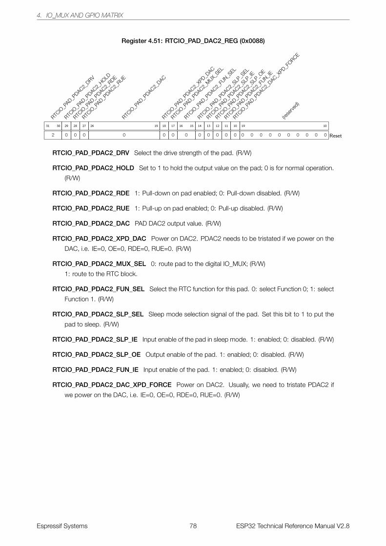
4. IO_MUX AND GPIO MATRIX
Register 4.51: RTCIO_PAD_DAC2_REG (0x0088)
RTCIO
_PAD_P
DAC2_DRV
2
31 30
RTCIO
_PAD_P
DAC2_HOLD
0
29
RTCIO
_PAD_P
DAC2_RDE
0
28
RTCIO
_PAD_P
DAC2_RUE
0
27
RTCIO
_PAD_P
DAC2_DAC
0
26 19
RTCIO
_PAD_P
DAC2_XP
D_DAC
0
18
RTCIO
_PAD_P
DAC2_M
UX_SEL
0
17
RTCIO
_PAD_P
DAC2_FU
N_SEL
0
16 15
RTCIO
_PAD_P
DAC2_SLP
_SEL
0
14
RTCIO
_PAD_P
DAC2_SLP
_IE
0
13
RTCIO
_PAD_P
DAC2_SLP
_OE
0
12
RTCIO
_PAD_P
DAC2_FU
N_IE
0
11
RTCIO
_PAD_P
DAC2_DAC_X
PD_FORCE
0
10
(rese
rved)
0 0 0 0 0 0 0 0 0 0
19 10
Reset
RTCIO_PAD_PDAC2_DRV Select the drive strength of the pad. (R/W)
RTCIO_PAD_PDAC2_HOLD Set to 1 to hold the output value on the pad; 0 is for normal operation.
(R/W)
RTCIO_PAD_PDAC2_RDE 1: Pull-down on pad enabled; 0: Pull-down disabled. (R/W)
RTCIO_PAD_PDAC2_RUE 1: Pull-up on pad enabled; 0: Pull-up disabled. (R/W)
RTCIO_PAD_PDAC2_DAC PAD DAC2 output value. (R/W)
RTCIO_PAD_PDAC2_XPD_DAC Power on DAC2. PDAC2 needs to be tristated if we power on the
DAC, i.e. IE=0, OE=0, RDE=0, RUE=0. (R/W)
RTCIO_PAD_PDAC2_MUX_SEL 0: route pad to the digital IO_MUX; (R/W)
1: route to the RTC block.
RTCIO_PAD_PDAC2_FUN_SEL Select the RTC function for this pad. 0: select Function 0; 1: select
Function 1. (R/W)
RTCIO_PAD_PDAC2_SLP_SEL Sleep mode selection signal of the pad. Set this bit to 1 to put the
pad to sleep. (R/W)
RTCIO_PAD_PDAC2_SLP_IE Input enable of the pad in sleep mode. 1: enabled; 0: disabled. (R/W)
RTCIO_PAD_PDAC2_SLP_OE Output enable of the pad. 1: enabled; 0: disabled. (R/W)
RTCIO_PAD_PDAC2_FUN_IE Input enable of the pad. 1: enabled; 0: disabled. (R/W)
RTCIO_PAD_PDAC2_DAC_XPD_FORCE Power on DAC2. Usually, we need to tristate PDAC2 if
we power on the DAC, i.e. IE=0, OE=0, RDE=0, RUE=0. (R/W)
Espressif Systems 78 ESP32 Technical Reference Manual V2.8
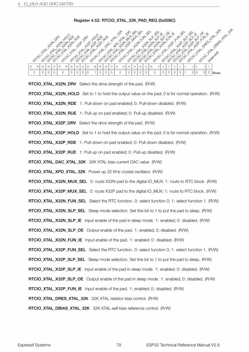
4. IO_MUX AND GPIO MATRIX
Register 4.52: RTCIO_XTAL_32K_PAD_REG (0x008C)
RTCIO
_XTA
L_X3
2N_D
RV
2
31 30
RTCIO
_XTA
L_X3
2N_H
OLD
0
29
RTCIO
_XTA
L_X3
2N_R
DE
0
28
RTCIO
_XTA
L_X3
2N_R
UE
0
27
RTCIO
_XTA
L_X3
2P_D
RV
2
26 25
RTCIO
_XTA
L_X3
2P_H
OLD
0
24
RTCIO
_XTA
L_X3
2P_R
DE
0
23
RTCIO
_XTA
L_X3
2P_R
UE
0
22
RTCIO
_XTA
L_DAC_X
TAL_
32K
0 1
21 20
RTCIO
_XTA
L_XP
D_XTA
L_32
K
0
19
RTCIO
_XTA
L_X3
2N_M
UX_SEL
0
18
RTCIO
_XTA
L_X3
2P_M
UX_SEL
0
17
RTCIO
_XTA
L_X3
2N_F
UN_SEL
0
16 15
RTCIO
_XTA
L_X3
2N_S
LP_S
EL
0
14
RTCIO
_XTA
L_X3
2N_S
LP_IE
0
13
RTCIO
_XTA
L_X3
2N_S
LP_O
E
0
12
RTCIO
_XTA
L_X3
2N_F
UN_IE
0
11
RTCIO
_XTA
L_X3
2P_F
UN_SEL
0
10 9
RTCIO
_XTA
L_X3
2P_S
LP_S
EL
0
8
RTCIO
_XTA
L_X3
2P_S
LP_IE
0
7
RTCIO
_XTA
L_X3
2P_S
LP_O
E
0
6
RTCIO
_XTA
L_X3
2P_F
UN_IE
0
5
RTCIO
_XTA
L_DRES_X
TAL_
32K
1 0
4 3
RTCIO
_XTA
L_DBIA
S_XTA
L_32
K
0 0
2 1
(rese
rved)
0
1
Reset
RTCIO_XTAL_X32N_DRV Select the drive strength of the pad. (R/W)
RTCIO_XTAL_X32N_HOLD Set to 1 to hold the output value on the pad; 0 is for normal operation. (R/W)
RTCIO_XTAL_X32N_RDE 1: Pull-down on pad enabled; 0: Pull-down disabled. (R/W)
RTCIO_XTAL_X32N_RUE 1: Pull-up on pad enabled; 0: Pull-up disabled. (R/W)
RTCIO_XTAL_X32P_DRV Select the drive strength of the pad. (R/W)
RTCIO_XTAL_X32P_HOLD Set to 1 to hold the output value on the pad, 0 is for normal operation. (R/W)
RTCIO_XTAL_X32P_RDE 1: Pull-down on pad enabled; 0: Pull-down disabled. (R/W)
RTCIO_XTAL_X32P_RUE 1: Pull-up on pad enabled; 0: Pull-up disabled. (R/W)
RTCIO_XTAL_DAC_XTAL_32K 32K XTAL bias current DAC value. (R/W)
RTCIO_XTAL_XPD_XTAL_32K Power up 32 KHz crystal oscillator. (R/W)
RTCIO_XTAL_X32N_MUX_SEL 0: route X32N pad to the digital IO_MUX; 1: route to RTC block. (R/W)
RTCIO_XTAL_X32P_MUX_SEL 0: route X32P pad to the digital IO_MUX; 1: route to RTC block. (R/W)
RTCIO_XTAL_X32N_FUN_SEL Select the RTC function. 0: select function 0; 1: select function 1. (R/W)
RTCIO_XTAL_X32N_SLP_SEL Sleep mode selection. Set this bit to 1 to put the pad to sleep. (R/W)
RTCIO_XTAL_X32N_SLP_IE Input enable of the pad in sleep mode. 1: enabled; 0: disabled. (R/W)
RTCIO_XTAL_X32N_SLP_OE Output enable of the pad. 1: enabled; 0; disabled. (R/W)
RTCIO_XTAL_X32N_FUN_IE Input enable of the pad. 1: enabled; 0: disabled. (R/W)
RTCIO_XTAL_X32P_FUN_SEL Select the RTC function. 0: select function 0; 1: select function 1. (R/W)
RTCIO_XTAL_X32P_SLP_SEL Sleep mode selection. Set this bit to 1 to put the pad to sleep. (R/W)
RTCIO_XTAL_X32P_SLP_IE Input enable of the pad in sleep mode. 1: enabled; 0: disabled. (R/W)
RTCIO_XTAL_X32P_SLP_OE Output enable of the pad in sleep mode. 1: enabled; 0: disabled. (R/W)
RTCIO_XTAL_X32P_FUN_IE Input enable of the pad. 1: enabled; 0: disabled. (R/W)
RTCIO_XTAL_DRES_XTAL_32K 32K XTAL resistor bias control. (R/W)
RTCIO_XTAL_DBIAS_XTAL_32K 32K XTAL self-bias reference control. (R/W)
Espressif Systems 79 ESP32 Technical Reference Manual V2.8
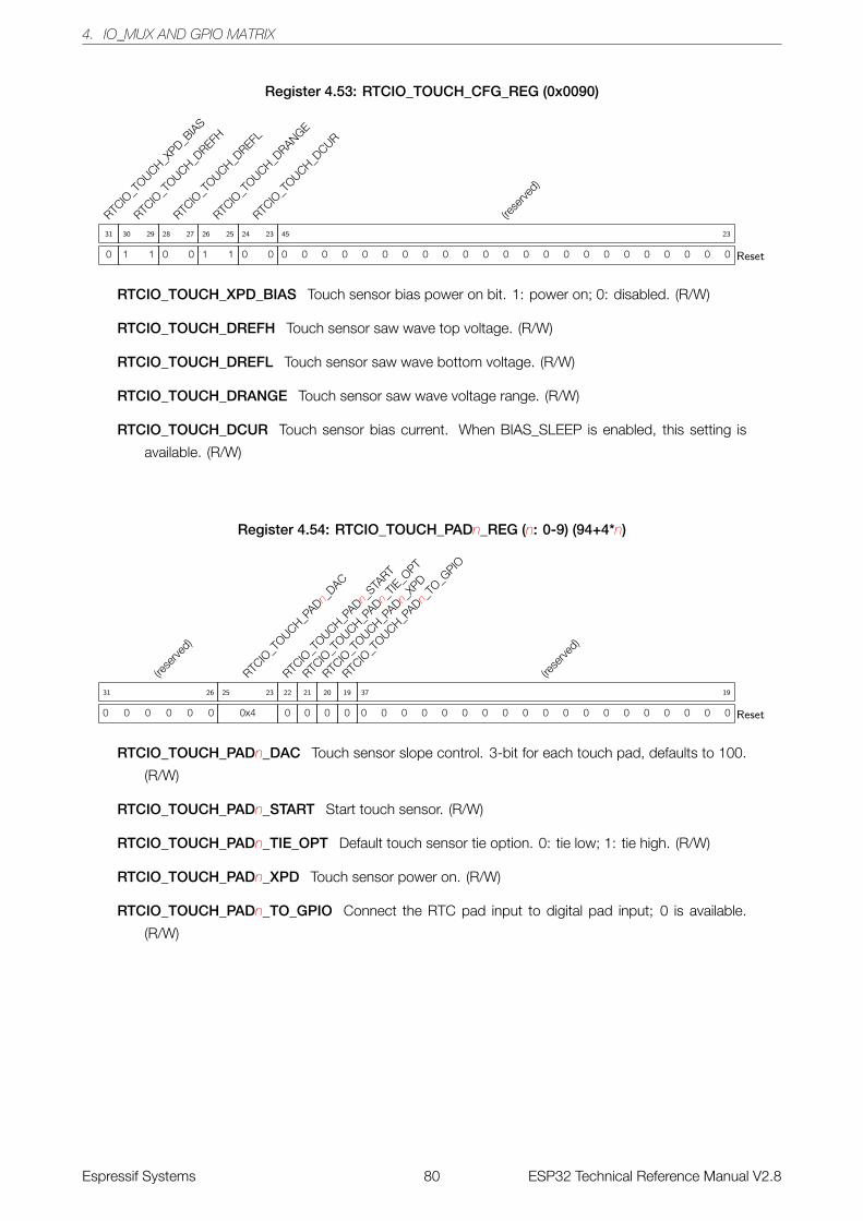
4. IO_MUX AND GPIO MATRIX
Register 4.53: RTCIO_TOUCH_CFG_REG (0x0090)
RTCIO
_TOUCH_X
PD_BIA
S
0
31
RTCIO
_TOUCH_D
REFH
1 1
30 29
RTCIO
_TOUCH_D
REFL
0 0
28 27
RTCIO
_TOUCH_D
RANGE
1 1
26 25
RTCIO
_TOUCH_D
CUR
0 0
24 23
(rese
rved)
0 0 0 0 0 0 0 0 0 0 0 0 0 0 0 0 0 0 0 0 0 0 0
45 23
Reset
RTCIO_TOUCH_XPD_BIAS Touch sensor bias power on bit. 1: power on; 0: disabled. (R/W)
RTCIO_TOUCH_DREFH Touch sensor saw wave top voltage. (R/W)
RTCIO_TOUCH_DREFL Touch sensor saw wave bottom voltage. (R/W)
RTCIO_TOUCH_DRANGE Touch sensor saw wave voltage range. (R/W)
RTCIO_TOUCH_DCUR Touch sensor bias current. When BIAS_SLEEP is enabled, this setting is
available. (R/W)
Register 4.54: RTCIO_TOUCH_PADn_REG (n: 0-9) (94+4*n)
(rese
rved)
0 0 0 0 0 0
31 26
RTCIO
_TOUCH_P
ADn_D
AC
0x4
25 23
RTCIO
_TOUCH_P
ADn_S
TART
0
22
RTCIO
_TOUCH_P
ADn_T
IE_OPT
0
21
RTCIO
_TOUCH_P
ADn_X
PD
0
20
RTCIO
_TOUCH_P
ADn_T
O_GPIO
0
19
(rese
rved)
0 0 0 0 0 0 0 0 0 0 0 0 0 0 0 0 0 0 0
37 19
Reset
RTCIO_TOUCH_PADn_DAC Touch sensor slope control. 3-bit for each touch pad, defaults to 100.
(R/W)
RTCIO_TOUCH_PADn_START Start touch sensor. (R/W)
RTCIO_TOUCH_PADn_TIE_OPT Default touch sensor tie option. 0: tie low; 1: tie high. (R/W)
RTCIO_TOUCH_PADn_XPD Touch sensor power on. (R/W)
RTCIO_TOUCH_PADn_TO_GPIO Connect the RTC pad input to digital pad input; 0 is available.
(R/W)
Espressif Systems 80 ESP32 Technical Reference Manual V2.8
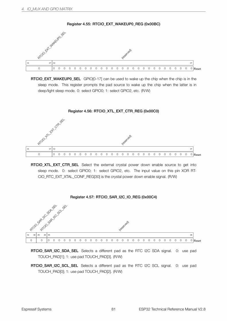
4. IO_MUX AND GPIO MATRIX
Register 4.55: RTCIO_EXT_WAKEUP0_REG (0x00BC)
RTCIO
_EXT
_WAKEUP0_
SEL
0
31 27
(rese
rved)
0 0 0 0 0 0 0 0 0 0 0 0 0 0 0 0 0 0 0 0 0 0 0 0 0 0 0
53 27
Reset
RTCIO_EXT_WAKEUP0_SEL GPIO[0-17] can be used to wake up the chip when the chip is in the
sleep mode. This register prompts the pad source to wake up the chip when the latter is in
deep/light sleep mode. 0: select GPIO0; 1: select GPIO2, etc. (R/W)
Register 4.56: RTCIO_XTL_EXT_CTR_REG (0x00C0)
RTCIO
_XTL
_EXT
_CTR
_SEL
0
31 27
(rese
rved)
0 0 0 0 0 0 0 0 0 0 0 0 0 0 0 0 0 0 0 0 0 0 0 0 0 0 0
53 27
Reset
RTCIO_XTL_EXT_CTR_SEL Select the external crystal power down enable source to get into
sleep mode. 0: select GPIO0; 1: select GPIO2, etc. The input value on this pin XOR RT-
CIO_RTC_EXT_XTAL_CONF_REG[30] is the crystal power down enable signal. (R/W)
Register 4.57: RTCIO_SAR_I2C_IO_REG (0x00C4)
RTCIO
_SAR_I2
C_SDA_S
EL
0
31 30
RTCIO
_SAR_I2
C_SCL_
SEL
0
29 28
(rese
rved)
0 0 0 0 0 0 0 0 0 0 0 0 0 0 0 0 0 0 0 0 0 0 0 0 0 0 0 0
55 28
Reset
RTCIO_SAR_I2C_SDA_SEL Selects a different pad as the RTC I2C SDA signal. 0: use pad
TOUCH_PAD[1]; 1: use pad TOUCH_PAD[3]. (R/W)
RTCIO_SAR_I2C_SCL_SEL Selects a different pad as the RTC I2C SCL signal. 0: use pad
TOUCH_PAD[0]; 1: use pad TOUCH_PAD[2]. (R/W)
Espressif Systems 81 ESP32 Technical Reference Manual V2.8

5. DPORT REGISTER
5. DPort Register
5.1 Introduction
The ESP32 integrates a large number of peripherals, and enables the control of individual peripherals to achieve
optimal characteristics in performance-vs-power-consumption scenarios. The DPort registers control clock
management (clock gating), power management, and the configuration of peripherals and core-system modules.
The system arranges each module with configuration registers contained in the DPort Register.
5.2 Features
DPort registers correspond to different peripheral blocks and core modules:
• System and memory
• Reset and clock
• Interrupt matrix
• DMA
• PID/MPU/MMU
• APP_CPU
• Peripheral clock gating and reset
5.3 Functional Description
5.3.1 System and Memory Register
The following registers are used for system and memory configuration, such as cache configuration and memory
remapping. For a detailed description of these registers, please refer to Chapter System and Memory.
• DPORT_PRO_BOOT_REMAP_CTRL_REG
• DPORT_APP_BOOT_REMAP_CTRL_REG
• DPORT_CACHE_MUX_MODE_REG
5.3.2 Reset and Clock Registers
The following register is used for Reset and Clock. For a detailed description of the register, please refer to Reset
and Clock.
• DPORT_CPU_PER_CONF_REG
Espressif Systems 82 ESP32 Technical Reference Manual V2.8
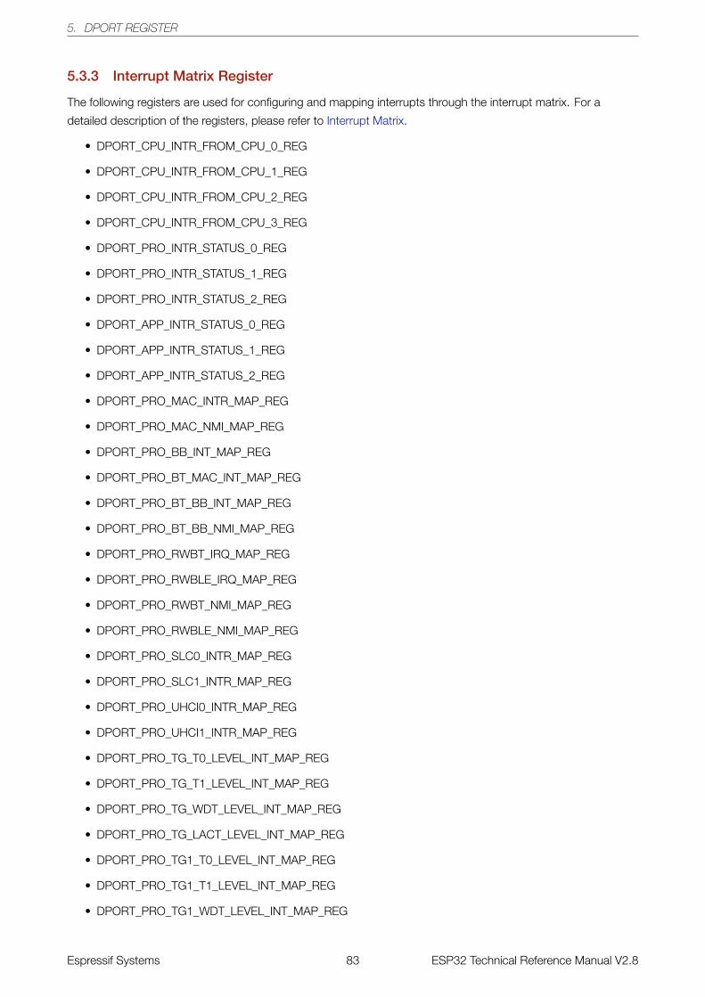
5. DPORT REGISTER
5.3.3 Interrupt Matrix Register
The following registers are used for configuring and mapping interrupts through the interrupt matrix. For a
detailed description of the registers, please refer to Interrupt Matrix.
• DPORT_CPU_INTR_FROM_CPU_0_REG
• DPORT_CPU_INTR_FROM_CPU_1_REG
• DPORT_CPU_INTR_FROM_CPU_2_REG
• DPORT_CPU_INTR_FROM_CPU_3_REG
• DPORT_PRO_INTR_STATUS_0_REG
• DPORT_PRO_INTR_STATUS_1_REG
• DPORT_PRO_INTR_STATUS_2_REG
• DPORT_APP_INTR_STATUS_0_REG
• DPORT_APP_INTR_STATUS_1_REG
• DPORT_APP_INTR_STATUS_2_REG
• DPORT_PRO_MAC_INTR_MAP_REG
• DPORT_PRO_MAC_NMI_MAP_REG
• DPORT_PRO_BB_INT_MAP_REG
• DPORT_PRO_BT_MAC_INT_MAP_REG
• DPORT_PRO_BT_BB_INT_MAP_REG
• DPORT_PRO_BT_BB_NMI_MAP_REG
• DPORT_PRO_RWBT_IRQ_MAP_REG
• DPORT_PRO_RWBLE_IRQ_MAP_REG
• DPORT_PRO_RWBT_NMI_MAP_REG
• DPORT_PRO_RWBLE_NMI_MAP_REG
• DPORT_PRO_SLC0_INTR_MAP_REG
• DPORT_PRO_SLC1_INTR_MAP_REG
• DPORT_PRO_UHCI0_INTR_MAP_REG
• DPORT_PRO_UHCI1_INTR_MAP_REG
• DPORT_PRO_TG_T0_LEVEL_INT_MAP_REG
• DPORT_PRO_TG_T1_LEVEL_INT_MAP_REG
• DPORT_PRO_TG_WDT_LEVEL_INT_MAP_REG
• DPORT_PRO_TG_LACT_LEVEL_INT_MAP_REG
• DPORT_PRO_TG1_T0_LEVEL_INT_MAP_REG
• DPORT_PRO_TG1_T1_LEVEL_INT_MAP_REG
• DPORT_PRO_TG1_WDT_LEVEL_INT_MAP_REG
Espressif Systems 83 ESP32 Technical Reference Manual V2.8
5. DPORT REGISTER
• DPORT_PRO_TG1_LACT_LEVEL_INT_MAP_REG
• DPORT_PRO_GPIO_INTERRUPT_MAP_REG
• DPORT_PRO_GPIO_INTERRUPT_NMI_MAP_REG
• DPORT_PRO_CPU_INTR_FROM_CPU_0_MAP_REG
• DPORT_PRO_CPU_INTR_FROM_CPU_1_MAP_REG
• DPORT_PRO_CPU_INTR_FROM_CPU_2_MAP_REG
• DPORT_PRO_CPU_INTR_FROM_CPU_3_MAP_REG
• DPORT_PRO_SPI_INTR_0_MAP_REG
• DPORT_PRO_SPI_INTR_1_MAP_REG
• DPORT_PRO_SPI_INTR_2_MAP_REG
• DPORT_PRO_SPI_INTR_3_MAP_REG
• DPORT_PRO_I2S0_INT_MAP_REG
• DPORT_PRO_I2S1_INT_MAP_REG
• DPORT_PRO_UART_INTR_MAP_REG
• DPORT_PRO_UART1_INTR_MAP_REG
• DPORT_PRO_UART2_INTR_MAP_REG
• DPORT_PRO_SDIO_HOST_INTERRUPT_MAP_REG
• DPORT_PRO_EMAC_INT_MAP_REG
• DPORT_PRO_PWM0_INTR_MAP_REG
• DPORT_PRO_PWM1_INTR_MAP_REG
• DPORT_PRO_PWM2_INTR_MAP_REG
• DPORT_PRO_PWM3_INTR_MAP_REG
• DPORT_PRO_LEDC_INT_MAP_REG
• DPORT_PRO_EFUSE_INT_MAP_REG
• DPORT_PRO_CAN_INT_MAP_REG
• DPORT_PRO_RTC_CORE_INTR_MAP_REG
• DPORT_PRO_RMT_INTR_MAP_REG
• DPORT_PRO_PCNT_INTR_MAP_REG
• DPORT_PRO_I2C_EXT0_INTR_MAP_REG
• DPORT_PRO_I2C_EXT1_INTR_MAP_REG
• DPORT_PRO_RSA_INTR_MAP_REG
• DPORT_PRO_SPI1_DMA_INT_MAP_REG
• DPORT_PRO_SPI2_DMA_INT_MAP_REG
• DPORT_PRO_SPI3_DMA_INT_MAP_REG
Espressif Systems 84 ESP32 Technical Reference Manual V2.8
5. DPORT REGISTER
• DPORT_PRO_WDG_INT_MAP_REG
• DPORT_PRO_TIMER_INT1_MAP_REG
• DPORT_PRO_TIMER_INT2_MAP_REG
• DPORT_PRO_TG_T0_EDGE_INT_MAP_REG
• DPORT_PRO_TG_T1_EDGE_INT_MAP_REG
• DPORT_PRO_TG_WDT_EDGE_INT_MAP_REG
• DPORT_PRO_TG_LACT_EDGE_INT_MAP_REG
• DPORT_PRO_TG1_T0_EDGE_INT_MAP_REG
• DPORT_PRO_TG1_T1_EDGE_INT_MAP_REG
• DPORT_PRO_TG1_WDT_EDGE_INT_MAP_REG
• DPORT_PRO_TG1_LACT_EDGE_INT_MAP_REG
• DPORT_PRO_MMU_IA_INT_MAP_REG
• DPORT_PRO_MPU_IA_INT_MAP_REG
• DPORT_PRO_CACHE_IA_INT_MAP_REG
• DPORT_APP_MAC_INTR_MAP_REG
• DPORT_APP_MAC_NMI_MAP_REG
• DPORT_APP_BB_INT_MAP_REG
• DPORT_APP_BT_MAC_INT_MAP_REG
• DPORT_APP_BT_BB_INT_MAP_REG
• DPORT_APP_BT_BB_NMI_MAP_REG
• DPORT_APP_RWBT_IRQ_MAP_REG
• DPORT_APP_RWBLE_IRQ_MAP_REG
• DPORT_APP_RWBT_NMI_MAP_REG
• DPORT_APP_RWBLE_NMI_MAP_REG
• DPORT_APP_SLC0_INTR_MAP_REG
• DPORT_APP_SLC1_INTR_MAP_REG
• DPORT_APP_UHCI0_INTR_MAP_REG
• DPORT_APP_UHCI1_INTR_MAP_REG
• DPORT_APP_TG_T0_LEVEL_INT_MAP_REG
• DPORT_APP_TG_T1_LEVEL_INT_MAP_REG
• DPORT_APP_TG_WDT_LEVEL_INT_MAP_REG
• DPORT_APP_TG_LACT_LEVEL_INT_MAP_REG
• DPORT_APP_TG1_T0_LEVEL_INT_MAP_REG
• DPORT_APP_TG1_T1_LEVEL_INT_MAP_REG
Espressif Systems 85 ESP32 Technical Reference Manual V2.8
5. DPORT REGISTER
• DPORT_APP_TG1_WDT_LEVEL_INT_MAP_REG
• DPORT_APP_TG1_LACT_LEVEL_INT_MAP_REG
• DPORT_APP_GPIO_INTERRUPT_MAP_REG
• DPORT_APP_GPIO_INTERRUPT_NMI_MAP_REG
• DPORT_APP_CPU_INTR_FROM_CPU_0_MAP_REG
• DPORT_APP_CPU_INTR_FROM_CPU_1_MAP_REG
• DPORT_APP_CPU_INTR_FROM_CPU_2_MAP_REG
• DPORT_APP_CPU_INTR_FROM_CPU_3_MAP_REG
• DPORT_APP_SPI_INTR_0_MAP_REG
• DPORT_APP_SPI_INTR_1_MAP_REG
• DPORT_APP_SPI_INTR_2_MAP_REG
• DPORT_APP_SPI_INTR_3_MAP_REG
• DPORT_APP_I2S0_INT_MAP_REG
• DPORT_APP_I2S1_INT_MAP_REG
• DPORT_APP_UART_INTR_MAP_REG
• DPORT_APP_UART1_INTR_MAP_REG
• DPORT_APP_UART2_INTR_MAP_REG
• DPORT_APP_SDIO_HOST_INTERRUPT_MAP_REG
• DPORT_APP_EMAC_INT_MAP_REG
• DPORT_APP_PWM0_INTR_MAP_REG
• DPORT_APP_PWM1_INTR_MAP_REG
• DPORT_APP_PWM2_INTR_MAP_REG
• DPORT_APP_PWM3_INTR_MAP_REG
• DPORT_APP_LEDC_INT_MAP_REG
• DPORT_APP_EFUSE_INT_MAP_REG
• DPORT_APP_CAN_INT_MAP_REG
• DPORT_APP_RTC_CORE_INTR_MAP_REG
• DPORT_APP_RMT_INTR_MAP_REG
• DPORT_APP_PCNT_INTR_MAP_REG
• DPORT_APP_I2C_EXT0_INTR_MAP_REG
• DPORT_APP_I2C_EXT1_INTR_MAP_REG
• DPORT_APP_RSA_INTR_MAP_REG
• DPORT_APP_SPI1_DMA_INT_MAP_REG
• DPORT_APP_SPI2_DMA_INT_MAP_REG
Espressif Systems 86 ESP32 Technical Reference Manual V2.8

5. DPORT REGISTER
• DPORT_APP_SPI3_DMA_INT_MAP_REG
• DPORT_APP_WDG_INT_MAP_REG
• DPORT_APP_TIMER_INT1_MAP_REG
• DPORT_APP_TIMER_INT2_MAP_REG
• DPORT_APP_TG_T0_EDGE_INT_MAP_REG
• DPORT_APP_TG_T1_EDGE_INT_MAP_REG
• DPORT_APP_TG_WDT_EDGE_INT_MAP_REG
• DPORT_APP_TG_LACT_EDGE_INT_MAP_REG
• DPORT_APP_TG1_T0_EDGE_INT_MAP_REG
• DPORT_APP_TG1_T1_EDGE_INT_MAP_REG
• DPORT_APP_TG1_WDT_EDGE_INT_MAP_REG
• DPORT_APP_TG1_LACT_EDGE_INT_MAP_REG
• DPORT_APP_MMU_IA_INT_MAP_REG
• DPORT_APP_MPU_IA_INT_MAP_REG
• DPORT_APP_CACHE_IA_INT_MAP_REG
5.3.4 DMA Registers
The following register is used for the SPI DMA configuration. For a detailed description of the register, please refer
to DMA.
• DPORT_SPI_DMA_CHAN_SEL_REG
5.3.5 PID/MPU/MMU Registers
The following registers are used for PID/MPU/MMU configuration and operation control. For a detailed
description of the registers, please refer to PID/MPU/MMU.
• DPORT_PRO_CACHE_CTRL_REG
• DPORT_APP_CACHE_CTRL_REG
• DPORT_IMMU_PAGE_MODE_REG
• DPORT_DMMU_PAGE_MODE_REG
• DPORT_AHB_MPU_TABLE_0_REG
• DPORT_AHB_MPU_TABLE_1_REG
• DPORT_AHBLITE_MPU_TABLE_UART_REG
• DPORT_AHBLITE_MPU_TABLE_SPI1_REG
• DPORT_AHBLITE_MPU_TABLE_SPI0_REG
• DPORT_AHBLITE_MPU_TABLE_GPIO_REG
• DPORT_AHBLITE_MPU_TABLE_FE2_REG
Espressif Systems 87 ESP32 Technical Reference Manual V2.8
5. DPORT REGISTER
• DPORT_AHBLITE_MPU_TABLE_FE_REG
• DPORT_AHBLITE_MPU_TABLE_TIMER_REG
• DPORT_AHBLITE_MPU_TABLE_RTC_REG
• DPORT_AHBLITE_MPU_TABLE_IO_MUX_REG
• DPORT_AHBLITE_MPU_TABLE_WDG_REG
• DPORT_AHBLITE_MPU_TABLE_HINF_REG
• DPORT_AHBLITE_MPU_TABLE_UHCI1_REG
• DPORT_AHBLITE_MPU_TABLE_I2S0_REG
• DPORT_AHBLITE_MPU_TABLE_UART1_REG
• DPORT_AHBLITE_MPU_TABLE_I2C_EXT0_REG
• DPORT_AHBLITE_MPU_TABLE_UHCI0_REG
• DPORT_AHBLITE_MPU_TABLE_SLCHOST_REG
• DPORT_AHBLITE_MPU_TABLE_RMT_REG
• DPORT_AHBLITE_MPU_TABLE_PCNT_REG
• DPORT_AHBLITE_MPU_TABLE_SLC_REG
• DPORT_AHBLITE_MPU_TABLE_LEDC_REG
• DPORT_AHBLITE_MPU_TABLE_EFUSE_REG
• DPORT_AHBLITE_MPU_TABLE_SPI_ENCRYPT_REG
• DPORT_AHBLITE_MPU_TABLE_PWM0_REG
• DPORT_AHBLITE_MPU_TABLE_TIMERGROUP_REG
• DPORT_AHBLITE_MPU_TABLE_TIMERGROUP1_REG
• DPORT_AHBLITE_MPU_TABLE_SPI2_REG
• DPORT_AHBLITE_MPU_TABLE_SPI3_REG
• DPORT_AHBLITE_MPU_TABLE_APB_CTRL_REG
• DPORT_AHBLITE_MPU_TABLE_I2C_EXT1_REG
• DPORT_AHBLITE_MPU_TABLE_SDIO_HOST_REG
• DPORT_AHBLITE_MPU_TABLE_EMAC_REG
• DPORT_AHBLITE_MPU_TABLE_PWM1_REG
• DPORT_AHBLITE_MPU_TABLE_I2S1_REG
• DPORT_AHBLITE_MPU_TABLE_UART2_REG
• DPORT_AHBLITE_MPU_TABLE_PWM2_REG
• DPORT_AHBLITE_MPU_TABLE_PWM3_REG
• DPORT_AHBLITE_MPU_TABLE_PWR_REG
• DPORT_IMMU_TABLE0_REG
Espressif Systems 88 ESP32 Technical Reference Manual V2.8
5. DPORT REGISTER
• DPORT_IMMU_TABLE1_REG
• DPORT_IMMU_TABLE2_REG
• DPORT_IMMU_TABLE3_REG
• DPORT_IMMU_TABLE4_REG
• DPORT_IMMU_TABLE5_REG
• DPORT_IMMU_TABLE6_REG
• DPORT_IMMU_TABLE7_REG
• DPORT_IMMU_TABLE8_REG
• DPORT_IMMU_TABLE9_REG
• DPORT_IMMU_TABLE10_REG
• DPORT_IMMU_TABLE11_REG
• DPORT_IMMU_TABLE12_REG
• DPORT_IMMU_TABLE13_REG
• DPORT_IMMU_TABLE14_REG
• DPORT_IMMU_TABLE15_REG
• DPORT_DMMU_TABLE0_REG
• DPORT_DMMU_TABLE1_REG
• DPORT_DMMU_TABLE2_REG
• DPORT_DMMU_TABLE3_REG
• DPORT_DMMU_TABLE4_REG
• DPORT_DMMU_TABLE5_REG
• DPORT_DMMU_TABLE6_REG
• DPORT_DMMU_TABLE7_REG
• DPORT_DMMU_TABLE8_REG
• DPORT_DMMU_TABLE9_REG
• DPORT_DMMU_TABLE10_REG
• DPORT_DMMU_TABLE11_REG
• DPORT_DMMU_TABLE12_REG
• DPORT_DMMU_TABLE13_REG
• DPORT_DMMU_TABLE14_REG
• DPORT_DMMU_TABLE15_REG
Espressif Systems 89 ESP32 Technical Reference Manual V2.8
5. DPORT REGISTER
5.3.6 APP_CPU Controller Registers
DPort registers are used for some basic configuration of the APP_CPU, such as performing a stalling execution,
and for configuring the ROM boot jump address.
• APP_CPU is reset when DPORT_APPCPU_RESETTING=1. It is released when
DPORT_APPCPU_RESETTING=0.
• When DPORT_APPCPU_CLKGATE_EN=0, the APP_CPU clock can be disabled to reduce power
consumption.
• When DPORT_APPCPU_RUNSTALL=1, the APP_CPU can be put into a stalled state.
• When APP_CPU is booted up with a ROM code, it will jump to the address stored in the
DPORT_APPCPU_BOOT_ADDR register.
5.3.7 Peripheral Clock Gating and Reset
Reset and clock gating registers covered in this section are active-high registers. Note that the reset bits are not
self-cleared by hardware. When a clock-gating register bit is set to 1, the corresponding clock is enabled. Setting
the register bit to 0 disables the clock. Setting a reset register bit to 1 puts the peripheral in a reset state, while
setting the register bit to 0 disables the reset state, thus enabling normal operation.
• DPORT_PERI_CLK_EN_REG: enables the hardware accelerator clock.
– BIT4, Digital Signature
– BIT3, Secure boot
– BIT2, RSA Accelerator
– BIT1, SHA Accelerator
– BIT0, AES Accelerator
• DPORT_PERI_RST_EN_REG: resets the accelerator.
– BIT4, Digital Signature
AES Accelerator and RSA Accelerator will also be reset.
– BIT3, Secure boot
AES Accelerator and SHA Accelerator will also be reset.
– BIT2, RSA Accelerator
– BIT1, SHA Accelerator
– BIT0, AES Accelerator
• DPORT_PERIP_CLK_EN_REG=1: enables the peripheral clock.
– BIT26, PWM3
– BIT25, PWM2
– BIT24, UART MEM
All UART-shared memory. As long as a UART is working, the UART memory clock cannot be in the
gating state.
– BIT23, UART2
Espressif Systems 90 ESP32 Technical Reference Manual V2.8

5. DPORT REGISTER
– BIT22, SPI_DMA
– BIT21, I2S1
– BIT20, PWM1
– BIT19, CAN
– BIT18, I2C1
– BIT17, PWM0
– BIT16, SPI3
– BIT15, Timer Group1
– BIT14, eFuse
– BIT13, Timer Group0
– BIT12, UHCI1
– BIT11, LED_PWM
– BIT10, PULSE_CNT
– BIT9, Remote Controller
– BIT8, UHCI0
– BIT7, I2C0
– BIT6, SPI2
– BIT5, UART1
– BIT4, I2S0
– BIT3, WDG
– BIT2, UART
– BIT1, SPI
– BIT0, Timers
• DPORT_PERIP_RST_EN_REG: resets peripherals
– BIT26, PWM3
– BIT25, PWM2
– BIT24, UART MEM
– BIT23, UART2
– BIT22, SPI_DMA
– BIT21, I2S1
– BIT20, PWM1
– BIT19, CAN
– BIT18, I2C1
– BIT17, PWM0
Espressif Systems 91 ESP32 Technical Reference Manual V2.8
5. DPORT REGISTER
– BIT16, SPI3
– BIT15, Timer Group1
– BIT14, eFuse
– BIT13, Timer Group0
– BIT12, UHCI1
– BIT11, LED_PWM
– BIT10, PULSE_CNT
– BIT9, Remote Controller
– BIT8, UHCI0
– BIT7, I2C0
– BIT6, SPI2
– BIT5, UART1
– BIT4, I2S0
– BIT3, WDG
– BIT2, UART
– BIT1, SPI
– BIT0, Timers
• DPORT_WIFI_CLK_EN_REG: used for Wi-Fi and BT clock gating.
• DPORT_WIFI_RST_EN_REG: used for Wi-Fi and BT reset.
Espressif Systems 92 ESP32 Technical Reference Manual V2.8
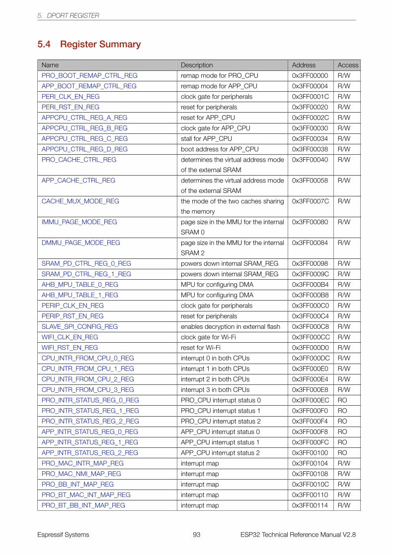
5. DPORT REGISTER
5.4 Register Summary
Name Description Address Access
PRO_BOOT_REMAP_CTRL_REG remap mode for PRO_CPU 0x3FF00000 R/W
APP_BOOT_REMAP_CTRL_REG remap mode for APP_CPU 0x3FF00004 R/W
PERI_CLK_EN_REG clock gate for peripherals 0x3FF0001C R/W
PERI_RST_EN_REG reset for peripherals 0x3FF00020 R/W
APPCPU_CTRL_REG_A_REG reset for APP_CPU 0x3FF0002C R/W
APPCPU_CTRL_REG_B_REG clock gate for APP_CPU 0x3FF00030 R/W
APPCPU_CTRL_REG_C_REG stall for APP_CPU 0x3FF00034 R/W
APPCPU_CTRL_REG_D_REG boot address for APP_CPU 0x3FF00038 R/W
PRO_CACHE_CTRL_REG determines the virtual address mode
of the external SRAM
0x3FF00040 R/W
APP_CACHE_CTRL_REG determines the virtual address mode
of the external SRAM
0x3FF00058 R/W
CACHE_MUX_MODE_REG the mode of the two caches sharing
the memory
0x3FF0007C R/W
IMMU_PAGE_MODE_REG page size in the MMU for the internal
SRAM 0
0x3FF00080 R/W
DMMU_PAGE_MODE_REG page size in the MMU for the internal
SRAM 2
0x3FF00084 R/W
SRAM_PD_CTRL_REG_0_REG powers down internal SRAM_REG 0x3FF00098 R/W
SRAM_PD_CTRL_REG_1_REG powers down internal SRAM_REG 0x3FF0009C R/W
AHB_MPU_TABLE_0_REG MPU for configuring DMA 0x3FF000B4 R/W
AHB_MPU_TABLE_1_REG MPU for configuring DMA 0x3FF000B8 R/W
PERIP_CLK_EN_REG clock gate for peripherals 0x3FF000C0 R/W
PERIP_RST_EN_REG reset for peripherals 0x3FF000C4 R/W
SLAVE_SPI_CONFIG_REG enables decryption in external flash 0x3FF000C8 R/W
WIFI_CLK_EN_REG clock gate for Wi-Fi 0x3FF000CC R/W
WIFI_RST_EN_REG reset for Wi-Fi 0x3FF000D0 R/W
CPU_INTR_FROM_CPU_0_REG interrupt 0 in both CPUs 0x3FF000DC R/W
CPU_INTR_FROM_CPU_1_REG interrupt 1 in both CPUs 0x3FF000E0 R/W
CPU_INTR_FROM_CPU_2_REG interrupt 2 in both CPUs 0x3FF000E4 R/W
CPU_INTR_FROM_CPU_3_REG interrupt 3 in both CPUs 0x3FF000E8 R/W
PRO_INTR_STATUS_REG_0_REG PRO_CPU interrupt status 0 0x3FF000EC RO
PRO_INTR_STATUS_REG_1_REG PRO_CPU interrupt status 1 0x3FF000F0 RO
PRO_INTR_STATUS_REG_2_REG PRO_CPU interrupt status 2 0x3FF000F4 RO
APP_INTR_STATUS_REG_0_REG APP_CPU interrupt status 0 0x3FF000F8 RO
APP_INTR_STATUS_REG_1_REG APP_CPU interrupt status 1 0x3FF000FC RO
APP_INTR_STATUS_REG_2_REG APP_CPU interrupt status 2 0x3FF00100 RO
PRO_MAC_INTR_MAP_REG interrupt map 0x3FF00104 R/W
PRO_MAC_NMI_MAP_REG interrupt map 0x3FF00108 R/W
PRO_BB_INT_MAP_REG interrupt map 0x3FF0010C R/W
PRO_BT_MAC_INT_MAP_REG interrupt map 0x3FF00110 R/W
PRO_BT_BB_INT_MAP_REG interrupt map 0x3FF00114 R/W
Espressif Systems 93 ESP32 Technical Reference Manual V2.8
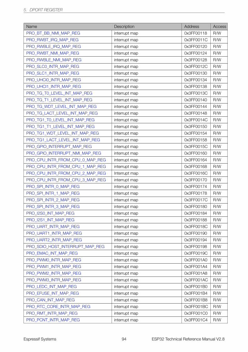
5. DPORT REGISTER
Name Description Address Access
PRO_BT_BB_NMI_MAP_REG interrupt map 0x3FF00118 R/W
PRO_RWBT_IRQ_MAP_REG interrupt map 0x3FF0011C R/W
PRO_RWBLE_IRQ_MAP_REG interrupt map 0x3FF00120 R/W
PRO_RWBT_NMI_MAP_REG interrupt map 0x3FF00124 R/W
PRO_RWBLE_NMI_MAP_REG interrupt map 0x3FF00128 R/W
PRO_SLC0_INTR_MAP_REG interrupt map 0x3FF0012C R/W
PRO_SLC1_INTR_MAP_REG interrupt map 0x3FF00130 R/W
PRO_UHCI0_INTR_MAP_REG interrupt map 0x3FF00134 R/W
PRO_UHCI1_INTR_MAP_REG interrupt map 0x3FF00138 R/W
PRO_TG_T0_LEVEL_INT_MAP_REG interrupt map 0x3FF0013C R/W
PRO_TG_T1_LEVEL_INT_MAP_REG interrupt map 0x3FF00140 R/W
PRO_TG_WDT_LEVEL_INT_MAP_REG interrupt map 0x3FF00144 R/W
PRO_TG_LACT_LEVEL_INT_MAP_REG interrupt map 0x3FF00148 R/W
PRO_TG1_T0_LEVEL_INT_MAP_REG interrupt map 0x3FF0014C R/W
PRO_TG1_T1_LEVEL_INT_MAP_REG interrupt map 0x3FF00150 R/W
PRO_TG1_WDT_LEVEL_INT_MAP_REG interrupt map 0x3FF00154 R/W
PRO_TG1_LACT_LEVEL_INT_MAP_REG interrupt map 0x3FF00158 R/W
PRO_GPIO_INTERRUPT_MAP_REG interrupt map 0x3FF0015C R/W
PRO_GPIO_INTERRUPT_NMI_MAP_REG interrupt map 0x3FF00160 R/W
PRO_CPU_INTR_FROM_CPU_0_MAP_REG interrupt map 0x3FF00164 R/W
PRO_CPU_INTR_FROM_CPU_1_MAP_REG interrupt map 0x3FF00168 R/W
PRO_CPU_INTR_FROM_CPU_2_MAP_REG Interrupt map 0x3FF0016C R/W
PRO_CPU_INTR_FROM_CPU_3_MAP_REG interrupt map 0x3FF00170 R/W
PRO_SPI_INTR_0_MAP_REG interrupt map 0x3FF00174 R/W
PRO_SPI_INTR_1_MAP_REG interrupt map 0x3FF00178 R/W
PRO_SPI_INTR_2_MAP_REG interrupt map 0x3FF0017C R/W
PRO_SPI_INTR_3_MAP_REG interrupt map 0x3FF00180 R/W
PRO_I2S0_INT_MAP_REG interrupt map 0x3FF00184 R/W
PRO_I2S1_INT_MAP_REG interrupt map 0x3FF00188 R/W
PRO_UART_INTR_MAP_REG interrupt map 0x3FF0018C R/W
PRO_UART1_INTR_MAP_REG interrupt map 0x3FF00190 R/W
PRO_UART2_INTR_MAP_REG interrupt map 0x3FF00194 R/W
PRO_SDIO_HOST_INTERRUPT_MAP_REG interrupt map 0x3FF00198 R/W
PRO_EMAC_INT_MAP_REG interrupt map 0x3FF0019C R/W
PRO_PWM0_INTR_MAP_REG interrupt map 0x3FF001A0 R/W
PRO_PWM1_INTR_MAP_REG interrupt map 0x3FF001A4 R/W
PRO_PWM2_INTR_MAP_REG interrupt map 0x3FF001A8 R/W
PRO_PWM3_INTR_MAP_REG interrupt map 0x3FF001AC R/W
PRO_LEDC_INT_MAP_REG interrupt map 0x3FF001B0 R/W
PRO_EFUSE_INT_MAP_REG interrupt map 0x3FF001B4 R/W
PRO_CAN_INT_MAP_REG interrupt map 0x3FF001B8 R/W
PRO_RTC_CORE_INTR_MAP_REG interrupt map 0x3FF001BC R/W
PRO_RMT_INTR_MAP_REG interrupt map 0x3FF001C0 R/W
PRO_PCNT_INTR_MAP_REG interrupt map 0x3FF001C4 R/W
Espressif Systems 94 ESP32 Technical Reference Manual V2.8
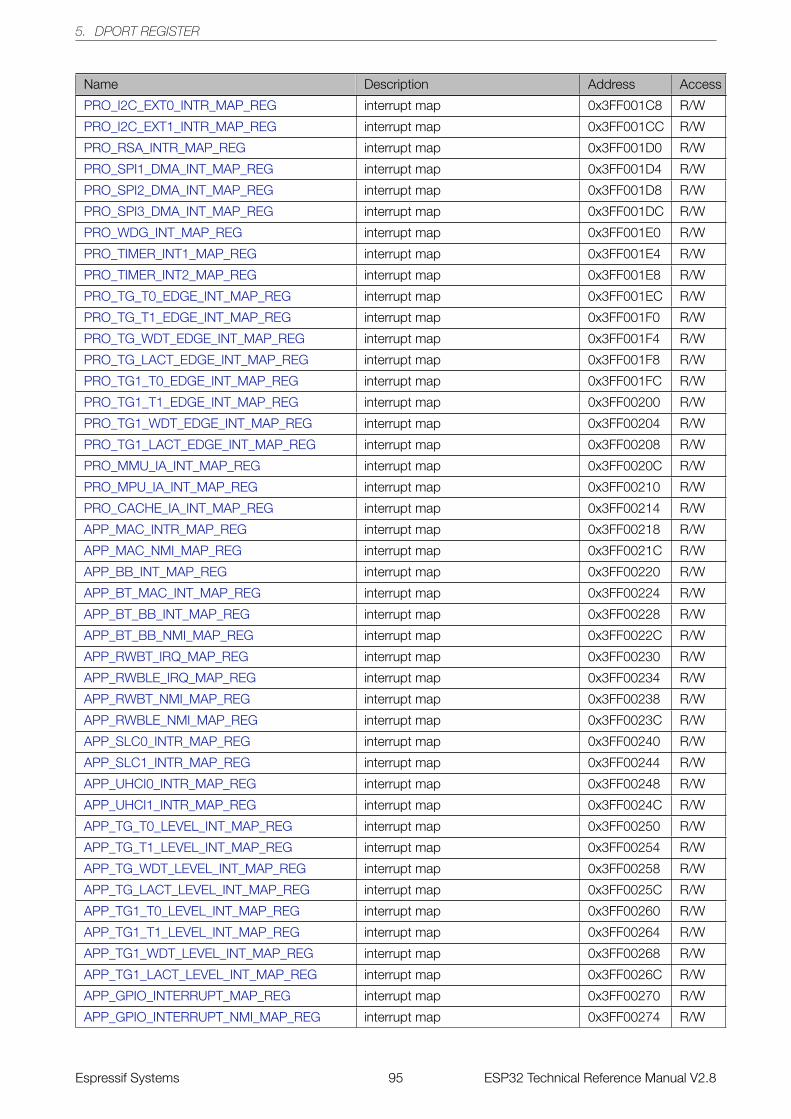
5. DPORT REGISTER
Name Description Address Access
PRO_I2C_EXT0_INTR_MAP_REG interrupt map 0x3FF001C8 R/W
PRO_I2C_EXT1_INTR_MAP_REG interrupt map 0x3FF001CC R/W
PRO_RSA_INTR_MAP_REG interrupt map 0x3FF001D0 R/W
PRO_SPI1_DMA_INT_MAP_REG interrupt map 0x3FF001D4 R/W
PRO_SPI2_DMA_INT_MAP_REG interrupt map 0x3FF001D8 R/W
PRO_SPI3_DMA_INT_MAP_REG interrupt map 0x3FF001DC R/W
PRO_WDG_INT_MAP_REG interrupt map 0x3FF001E0 R/W
PRO_TIMER_INT1_MAP_REG interrupt map 0x3FF001E4 R/W
PRO_TIMER_INT2_MAP_REG interrupt map 0x3FF001E8 R/W
PRO_TG_T0_EDGE_INT_MAP_REG interrupt map 0x3FF001EC R/W
PRO_TG_T1_EDGE_INT_MAP_REG interrupt map 0x3FF001F0 R/W
PRO_TG_WDT_EDGE_INT_MAP_REG interrupt map 0x3FF001F4 R/W
PRO_TG_LACT_EDGE_INT_MAP_REG interrupt map 0x3FF001F8 R/W
PRO_TG1_T0_EDGE_INT_MAP_REG interrupt map 0x3FF001FC R/W
PRO_TG1_T1_EDGE_INT_MAP_REG interrupt map 0x3FF00200 R/W
PRO_TG1_WDT_EDGE_INT_MAP_REG interrupt map 0x3FF00204 R/W
PRO_TG1_LACT_EDGE_INT_MAP_REG interrupt map 0x3FF00208 R/W
PRO_MMU_IA_INT_MAP_REG interrupt map 0x3FF0020C R/W
PRO_MPU_IA_INT_MAP_REG interrupt map 0x3FF00210 R/W
PRO_CACHE_IA_INT_MAP_REG interrupt map 0x3FF00214 R/W
APP_MAC_INTR_MAP_REG interrupt map 0x3FF00218 R/W
APP_MAC_NMI_MAP_REG interrupt map 0x3FF0021C R/W
APP_BB_INT_MAP_REG interrupt map 0x3FF00220 R/W
APP_BT_MAC_INT_MAP_REG interrupt map 0x3FF00224 R/W
APP_BT_BB_INT_MAP_REG interrupt map 0x3FF00228 R/W
APP_BT_BB_NMI_MAP_REG interrupt map 0x3FF0022C R/W
APP_RWBT_IRQ_MAP_REG interrupt map 0x3FF00230 R/W
APP_RWBLE_IRQ_MAP_REG interrupt map 0x3FF00234 R/W
APP_RWBT_NMI_MAP_REG interrupt map 0x3FF00238 R/W
APP_RWBLE_NMI_MAP_REG interrupt map 0x3FF0023C R/W
APP_SLC0_INTR_MAP_REG interrupt map 0x3FF00240 R/W
APP_SLC1_INTR_MAP_REG interrupt map 0x3FF00244 R/W
APP_UHCI0_INTR_MAP_REG interrupt map 0x3FF00248 R/W
APP_UHCI1_INTR_MAP_REG interrupt map 0x3FF0024C R/W
APP_TG_T0_LEVEL_INT_MAP_REG interrupt map 0x3FF00250 R/W
APP_TG_T1_LEVEL_INT_MAP_REG interrupt map 0x3FF00254 R/W
APP_TG_WDT_LEVEL_INT_MAP_REG interrupt map 0x3FF00258 R/W
APP_TG_LACT_LEVEL_INT_MAP_REG interrupt map 0x3FF0025C R/W
APP_TG1_T0_LEVEL_INT_MAP_REG interrupt map 0x3FF00260 R/W
APP_TG1_T1_LEVEL_INT_MAP_REG interrupt map 0x3FF00264 R/W
APP_TG1_WDT_LEVEL_INT_MAP_REG interrupt map 0x3FF00268 R/W
APP_TG1_LACT_LEVEL_INT_MAP_REG interrupt map 0x3FF0026C R/W
APP_GPIO_INTERRUPT_MAP_REG interrupt map 0x3FF00270 R/W
APP_GPIO_INTERRUPT_NMI_MAP_REG interrupt map 0x3FF00274 R/W
Espressif Systems 95 ESP32 Technical Reference Manual V2.8
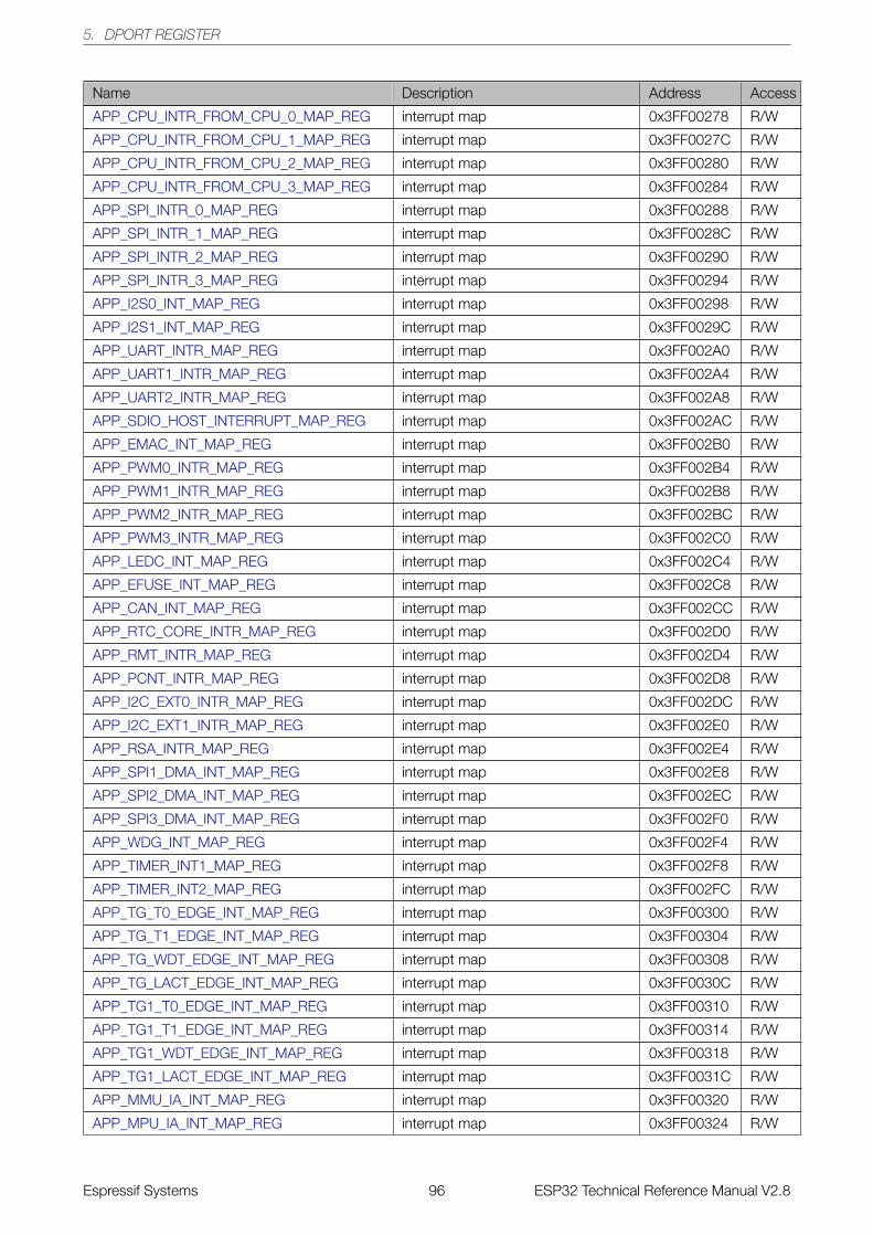
5. DPORT REGISTER
Name Description Address Access
APP_CPU_INTR_FROM_CPU_0_MAP_REG interrupt map 0x3FF00278 R/W
APP_CPU_INTR_FROM_CPU_1_MAP_REG interrupt map 0x3FF0027C R/W
APP_CPU_INTR_FROM_CPU_2_MAP_REG interrupt map 0x3FF00280 R/W
APP_CPU_INTR_FROM_CPU_3_MAP_REG interrupt map 0x3FF00284 R/W
APP_SPI_INTR_0_MAP_REG interrupt map 0x3FF00288 R/W
APP_SPI_INTR_1_MAP_REG interrupt map 0x3FF0028C R/W
APP_SPI_INTR_2_MAP_REG interrupt map 0x3FF00290 R/W
APP_SPI_INTR_3_MAP_REG interrupt map 0x3FF00294 R/W
APP_I2S0_INT_MAP_REG interrupt map 0x3FF00298 R/W
APP_I2S1_INT_MAP_REG interrupt map 0x3FF0029C R/W
APP_UART_INTR_MAP_REG interrupt map 0x3FF002A0 R/W
APP_UART1_INTR_MAP_REG interrupt map 0x3FF002A4 R/W
APP_UART2_INTR_MAP_REG interrupt map 0x3FF002A8 R/W
APP_SDIO_HOST_INTERRUPT_MAP_REG interrupt map 0x3FF002AC R/W
APP_EMAC_INT_MAP_REG interrupt map 0x3FF002B0 R/W
APP_PWM0_INTR_MAP_REG interrupt map 0x3FF002B4 R/W
APP_PWM1_INTR_MAP_REG interrupt map 0x3FF002B8 R/W
APP_PWM2_INTR_MAP_REG interrupt map 0x3FF002BC R/W
APP_PWM3_INTR_MAP_REG interrupt map 0x3FF002C0 R/W
APP_LEDC_INT_MAP_REG interrupt map 0x3FF002C4 R/W
APP_EFUSE_INT_MAP_REG interrupt map 0x3FF002C8 R/W
APP_CAN_INT_MAP_REG interrupt map 0x3FF002CC R/W
APP_RTC_CORE_INTR_MAP_REG interrupt map 0x3FF002D0 R/W
APP_RMT_INTR_MAP_REG interrupt map 0x3FF002D4 R/W
APP_PCNT_INTR_MAP_REG interrupt map 0x3FF002D8 R/W
APP_I2C_EXT0_INTR_MAP_REG interrupt map 0x3FF002DC R/W
APP_I2C_EXT1_INTR_MAP_REG interrupt map 0x3FF002E0 R/W
APP_RSA_INTR_MAP_REG interrupt map 0x3FF002E4 R/W
APP_SPI1_DMA_INT_MAP_REG interrupt map 0x3FF002E8 R/W
APP_SPI2_DMA_INT_MAP_REG interrupt map 0x3FF002EC R/W
APP_SPI3_DMA_INT_MAP_REG interrupt map 0x3FF002F0 R/W
APP_WDG_INT_MAP_REG interrupt map 0x3FF002F4 R/W
APP_TIMER_INT1_MAP_REG interrupt map 0x3FF002F8 R/W
APP_TIMER_INT2_MAP_REG interrupt map 0x3FF002FC R/W
APP_TG_T0_EDGE_INT_MAP_REG interrupt map 0x3FF00300 R/W
APP_TG_T1_EDGE_INT_MAP_REG interrupt map 0x3FF00304 R/W
APP_TG_WDT_EDGE_INT_MAP_REG interrupt map 0x3FF00308 R/W
APP_TG_LACT_EDGE_INT_MAP_REG interrupt map 0x3FF0030C R/W
APP_TG1_T0_EDGE_INT_MAP_REG interrupt map 0x3FF00310 R/W
APP_TG1_T1_EDGE_INT_MAP_REG interrupt map 0x3FF00314 R/W
APP_TG1_WDT_EDGE_INT_MAP_REG interrupt map 0x3FF00318 R/W
APP_TG1_LACT_EDGE_INT_MAP_REG interrupt map 0x3FF0031C R/W
APP_MMU_IA_INT_MAP_REG interrupt map 0x3FF00320 R/W
APP_MPU_IA_INT_MAP_REG interrupt map 0x3FF00324 R/W
Espressif Systems 96 ESP32 Technical Reference Manual V2.8
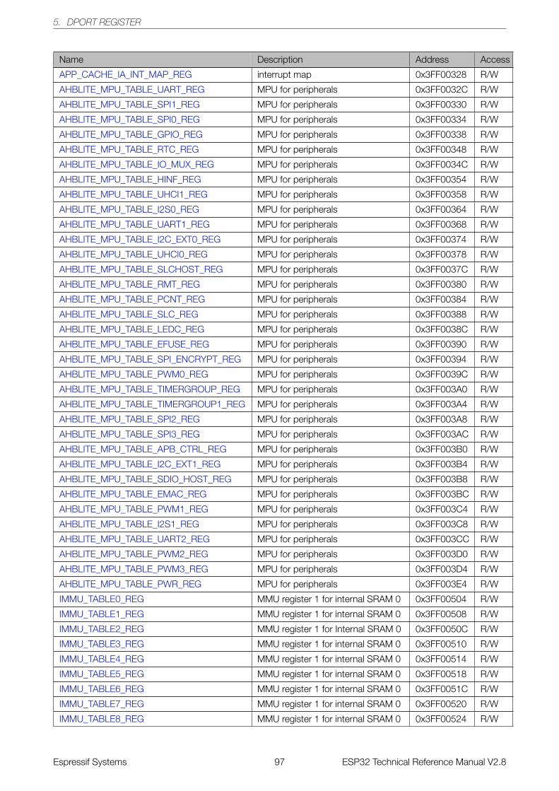
5. DPORT REGISTER
Name Description Address Access
APP_CACHE_IA_INT_MAP_REG interrupt map 0x3FF00328 R/W
AHBLITE_MPU_TABLE_UART_REG MPU for peripherals 0x3FF0032C R/W
AHBLITE_MPU_TABLE_SPI1_REG MPU for peripherals 0x3FF00330 R/W
AHBLITE_MPU_TABLE_SPI0_REG MPU for peripherals 0x3FF00334 R/W
AHBLITE_MPU_TABLE_GPIO_REG MPU for peripherals 0x3FF00338 R/W
AHBLITE_MPU_TABLE_RTC_REG MPU for peripherals 0x3FF00348 R/W
AHBLITE_MPU_TABLE_IO_MUX_REG MPU for peripherals 0x3FF0034C R/W
AHBLITE_MPU_TABLE_HINF_REG MPU for peripherals 0x3FF00354 R/W
AHBLITE_MPU_TABLE_UHCI1_REG MPU for peripherals 0x3FF00358 R/W
AHBLITE_MPU_TABLE_I2S0_REG MPU for peripherals 0x3FF00364 R/W
AHBLITE_MPU_TABLE_UART1_REG MPU for peripherals 0x3FF00368 R/W
AHBLITE_MPU_TABLE_I2C_EXT0_REG MPU for peripherals 0x3FF00374 R/W
AHBLITE_MPU_TABLE_UHCI0_REG MPU for peripherals 0x3FF00378 R/W
AHBLITE_MPU_TABLE_SLCHOST_REG MPU for peripherals 0x3FF0037C R/W
AHBLITE_MPU_TABLE_RMT_REG MPU for peripherals 0x3FF00380 R/W
AHBLITE_MPU_TABLE_PCNT_REG MPU for peripherals 0x3FF00384 R/W
AHBLITE_MPU_TABLE_SLC_REG MPU for peripherals 0x3FF00388 R/W
AHBLITE_MPU_TABLE_LEDC_REG MPU for peripherals 0x3FF0038C R/W
AHBLITE_MPU_TABLE_EFUSE_REG MPU for peripherals 0x3FF00390 R/W
AHBLITE_MPU_TABLE_SPI_ENCRYPT_REG MPU for peripherals 0x3FF00394 R/W
AHBLITE_MPU_TABLE_PWM0_REG MPU for peripherals 0x3FF0039C R/W
AHBLITE_MPU_TABLE_TIMERGROUP_REG MPU for peripherals 0x3FF003A0 R/W
AHBLITE_MPU_TABLE_TIMERGROUP1_REG MPU for peripherals 0x3FF003A4 R/W
AHBLITE_MPU_TABLE_SPI2_REG MPU for peripherals 0x3FF003A8 R/W
AHBLITE_MPU_TABLE_SPI3_REG MPU for peripherals 0x3FF003AC R/W
AHBLITE_MPU_TABLE_APB_CTRL_REG MPU for peripherals 0x3FF003B0 R/W
AHBLITE_MPU_TABLE_I2C_EXT1_REG MPU for peripherals 0x3FF003B4 R/W
AHBLITE_MPU_TABLE_SDIO_HOST_REG MPU for peripherals 0x3FF003B8 R/W
AHBLITE_MPU_TABLE_EMAC_REG MPU for peripherals 0x3FF003BC R/W
AHBLITE_MPU_TABLE_PWM1_REG MPU for peripherals 0x3FF003C4 R/W
AHBLITE_MPU_TABLE_I2S1_REG MPU for peripherals 0x3FF003C8 R/W
AHBLITE_MPU_TABLE_UART2_REG MPU for peripherals 0x3FF003CC R/W
AHBLITE_MPU_TABLE_PWM2_REG MPU for peripherals 0x3FF003D0 R/W
AHBLITE_MPU_TABLE_PWM3_REG MPU for peripherals 0x3FF003D4 R/W
AHBLITE_MPU_TABLE_PWR_REG MPU for peripherals 0x3FF003E4 R/W
IMMU_TABLE0_REG MMU register 1 for internal SRAM 0 0x3FF00504 R/W
IMMU_TABLE1_REG MMU register 1 for internal SRAM 0 0x3FF00508 R/W
IMMU_TABLE2_REG MMU register 1 for Internal SRAM 0 0x3FF0050C R/W
IMMU_TABLE3_REG MMU register 1 for internal SRAM 0 0x3FF00510 R/W
IMMU_TABLE4_REG MMU register 1 for internal SRAM 0 0x3FF00514 R/W
IMMU_TABLE5_REG MMU register 1 for internal SRAM 0 0x3FF00518 R/W
IMMU_TABLE6_REG MMU register 1 for internal SRAM 0 0x3FF0051C R/W
IMMU_TABLE7_REG MMU register 1 for internal SRAM 0 0x3FF00520 R/W
IMMU_TABLE8_REG MMU register 1 for internal SRAM 0 0x3FF00524 R/W
Espressif Systems 97 ESP32 Technical Reference Manual V2.8
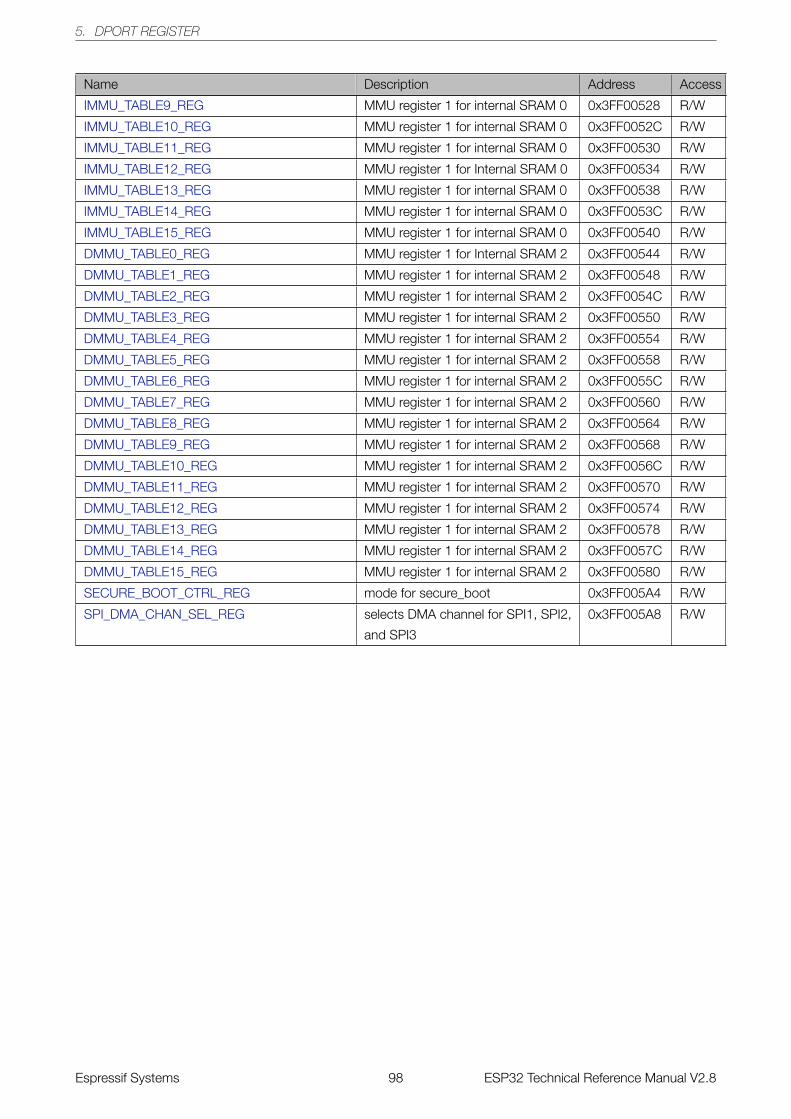
5. DPORT REGISTER
Name Description Address Access
IMMU_TABLE9_REG MMU register 1 for internal SRAM 0 0x3FF00528 R/W
IMMU_TABLE10_REG MMU register 1 for internal SRAM 0 0x3FF0052C R/W
IMMU_TABLE11_REG MMU register 1 for internal SRAM 0 0x3FF00530 R/W
IMMU_TABLE12_REG MMU register 1 for Internal SRAM 0 0x3FF00534 R/W
IMMU_TABLE13_REG MMU register 1 for internal SRAM 0 0x3FF00538 R/W
IMMU_TABLE14_REG MMU register 1 for internal SRAM 0 0x3FF0053C R/W
IMMU_TABLE15_REG MMU register 1 for internal SRAM 0 0x3FF00540 R/W
DMMU_TABLE0_REG MMU register 1 for Internal SRAM 2 0x3FF00544 R/W
DMMU_TABLE1_REG MMU register 1 for internal SRAM 2 0x3FF00548 R/W
DMMU_TABLE2_REG MMU register 1 for internal SRAM 2 0x3FF0054C R/W
DMMU_TABLE3_REG MMU register 1 for internal SRAM 2 0x3FF00550 R/W
DMMU_TABLE4_REG MMU register 1 for internal SRAM 2 0x3FF00554 R/W
DMMU_TABLE5_REG MMU register 1 for internal SRAM 2 0x3FF00558 R/W
DMMU_TABLE6_REG MMU register 1 for internal SRAM 2 0x3FF0055C R/W
DMMU_TABLE7_REG MMU register 1 for internal SRAM 2 0x3FF00560 R/W
DMMU_TABLE8_REG MMU register 1 for internal SRAM 2 0x3FF00564 R/W
DMMU_TABLE9_REG MMU register 1 for internal SRAM 2 0x3FF00568 R/W
DMMU_TABLE10_REG MMU register 1 for internal SRAM 2 0x3FF0056C R/W
DMMU_TABLE11_REG MMU register 1 for internal SRAM 2 0x3FF00570 R/W
DMMU_TABLE12_REG MMU register 1 for internal SRAM 2 0x3FF00574 R/W
DMMU_TABLE13_REG MMU register 1 for internal SRAM 2 0x3FF00578 R/W
DMMU_TABLE14_REG MMU register 1 for internal SRAM 2 0x3FF0057C R/W
DMMU_TABLE15_REG MMU register 1 for internal SRAM 2 0x3FF00580 R/W
SECURE_BOOT_CTRL_REG mode for secure_boot 0x3FF005A4 R/W
SPI_DMA_CHAN_SEL_REG selects DMA channel for SPI1, SPI2,
and SPI3
0x3FF005A8 R/W
Espressif Systems 98 ESP32 Technical Reference Manual V2.8
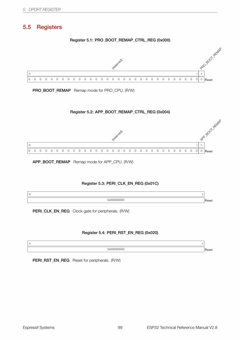
5. DPORT REGISTER
5.5 Registers
Register 5.1: PRO_BOOT_REMAP_CTRL_REG (0x000)
(rese
rved)
0 0 0 0 0 0 0 0 0 0 0 0 0 0 0 0 0 0 0 0 0 0 0 0 0 0 0 0 0 0 0
31 1
PRO_BOOT_
REMAP
0
0
Reset
PRO_BOOT_REMAP Remap mode for PRO_CPU. (R/W)
Register 5.2: APP_BOOT_REMAP_CTRL_REG (0x004)
(rese
rved)
0 0 0 0 0 0 0 0 0 0 0 0 0 0 0 0 0 0 0 0 0 0 0 0 0 0 0 0 0 0 0
31 1
APP_BOOT_
REMAP
0
0
Reset
APP_BOOT_REMAP Remap mode for APP_CPU. (R/W)
Register 5.3: PERI_CLK_EN_REG (0x01C)
0x000000000
31 0
Reset
PERI_CLK_EN_REG Clock gate for peripherals. (R/W)
Register 5.4: PERI_RST_EN_REG (0x020)
0x000000000
31 0
Reset
PERI_RST_EN_REG Reset for peripherals. (R/W)
Espressif Systems 99 ESP32 Technical Reference Manual V2.8
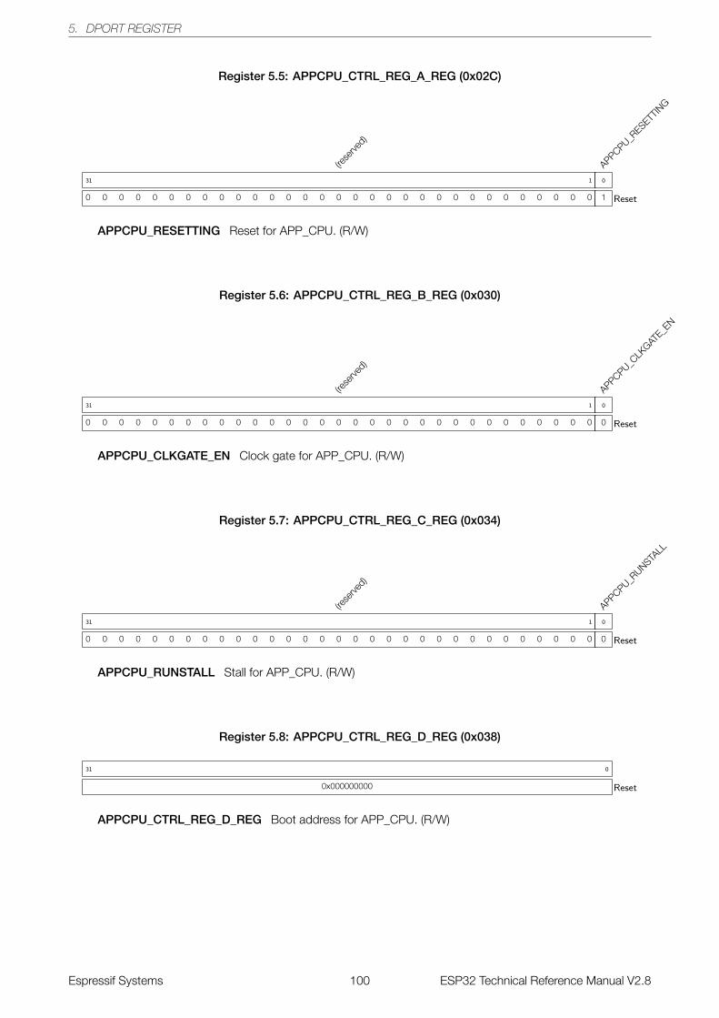
5. DPORT REGISTER
Register 5.5: APPCPU_CTRL_REG_A_REG (0x02C)
(rese
rved)
0 0 0 0 0 0 0 0 0 0 0 0 0 0 0 0 0 0 0 0 0 0 0 0 0 0 0 0 0 0 0
31 1
APPCPU_RESETT
ING
1
0
Reset
APPCPU_RESETTING Reset for APP_CPU. (R/W)
Register 5.6: APPCPU_CTRL_REG_B_REG (0x030)
(rese
rved)
0 0 0 0 0 0 0 0 0 0 0 0 0 0 0 0 0 0 0 0 0 0 0 0 0 0 0 0 0 0 0
31 1
APPCPU_CLK
GATE_E
N
0
0
Reset
APPCPU_CLKGATE_EN Clock gate for APP_CPU. (R/W)
Register 5.7: APPCPU_CTRL_REG_C_REG (0x034)
(rese
rved)
0 0 0 0 0 0 0 0 0 0 0 0 0 0 0 0 0 0 0 0 0 0 0 0 0 0 0 0 0 0 0
31 1
APPCPU_RUNSTA
LL
0
0
Reset
APPCPU_RUNSTALL Stall for APP_CPU. (R/W)
Register 5.8: APPCPU_CTRL_REG_D_REG (0x038)
0x000000000
31 0
Reset
APPCPU_CTRL_REG_D_REG Boot address for APP_CPU. (R/W)
Espressif Systems 100 ESP32 Technical Reference Manual V2.8
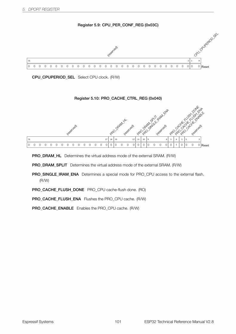
5. DPORT REGISTER
Register 5.9: CPU_PER_CONF_REG (0x03C)
(rese
rved)
0 0 0 0 0 0 0 0 0 0 0 0 0 0 0 0 0 0 0 0 0 0 0 0 0 0 0 0 0 0
31 2
CPU_CPUPERIO
D_SEL
0 0
1 0
Reset
CPU_CPUPERIOD_SEL Select CPU clock. (R/W)
Register 5.10: PRO_CACHE_CTRL_REG (0x040)
(rese
rved)
0 0 0 0 0 0 0 0 0 0 0 0 0 0 0
31 17
PRO_DRAM
_HL
0
16
(rese
rved)
0 0 0 0
15 12
PRO_DRAM
_SPLIT
0
11
PRO_SIN
GLE_IR
AM_E
NA
0
10
(rese
rved)
0 0 0 0
9 6
PRO_CACHE_F
LUSH_D
ONE
0
5
PRO_CACHE_F
LUSH_E
NA
1
4
PRO_CACHE_E
NABLE
0
3
(rese
rved)
0 0 0
5 3
Reset
PRO_DRAM_HL Determines the virtual address mode of the external SRAM. (R/W)
PRO_DRAM_SPLIT Determines the virtual address mode of the external SRAM. (R/W)
PRO_SINGLE_IRAM_ENA Determines a special mode for PRO_CPU access to the external flash.
(R/W)
PRO_CACHE_FLUSH_DONE PRO_CPU cache-flush done. (RO)
PRO_CACHE_FLUSH_ENA Flushes the PRO_CPU cache. (R/W)
PRO_CACHE_ENABLE Enables the PRO_CPU cache. (R/W)
Espressif Systems 101 ESP32 Technical Reference Manual V2.8
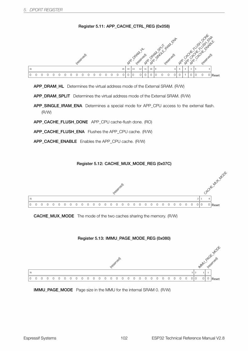
5. DPORT REGISTER
Register 5.11: APP_CACHE_CTRL_REG (0x058)
(rese
rved)
0 0 0 0 0 0 0 0 0 0 0 0 0 0 0 0 0
31 15
APP_DRAM
_HL
0
14
(rese
rved)
0 0
13 12
APP_DRAM
_SPLIT
0
11
APP_SIN
GLE_IR
AM_E
NA
0
10
(rese
rved)
0 0 0 0
9 6
APP_CACHE_F
LUSH_D
ONE
0
5
APP_CACHE_F
LUSH_E
NA
1
4
APP_CACHE_E
NABLE
0
3
(rese
rved)
0 0 0
5 3
Reset
APP_DRAM_HL Determines the virtual address mode of the External SRAM. (R/W)
APP_DRAM_SPLIT Determines the virtual address mode of the External SRAM. (R/W)
APP_SINGLE_IRAM_ENA Determines a special mode for APP_CPU access to the external flash.
(R/W)
APP_CACHE_FLUSH_DONE APP_CPU cache-flush done. (RO)
APP_CACHE_FLUSH_ENA Flushes the APP_CPU cache. (R/W)
APP_CACHE_ENABLE Enables the APP_CPU cache. (R/W)
Register 5.12: CACHE_MUX_MODE_REG (0x07C)
(rese
rved)
0 0 0 0 0 0 0 0 0 0 0 0 0 0 0 0 0 0 0 0 0 0 0 0 0 0 0 0 0 0
31 2
CACHE_MUX_
MODE
0 0
1 0
Reset
CACHE_MUX_MODE The mode of the two caches sharing the memory. (R/W)
Register 5.13: IMMU_PAGE_MODE_REG (0x080)
(rese
rved)
0 0 0 0 0 0 0 0 0 0 0 0 0 0 0 0 0 0 0 0 0 0 0 0 0 0 0 0 0
31 3
IMM
U_PAGE_M
ODE
0 0
2 1
(rese
rved)
0
1
Reset
IMMU_PAGE_MODE Page size in the MMU for the internal SRAM 0. (R/W)
Espressif Systems 102 ESP32 Technical Reference Manual V2.8
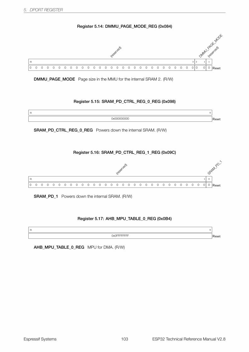
5. DPORT REGISTER
Register 5.14: DMMU_PAGE_MODE_REG (0x084)
(rese
rved)
0 0 0 0 0 0 0 0 0 0 0 0 0 0 0 0 0 0 0 0 0 0 0 0 0 0 0 0 0
31 3
DMM
U_PAGE_M
ODE
0 0
2 1
(rese
rved)
0
1
Reset
DMMU_PAGE_MODE Page size in the MMU for the internal SRAM 2. (R/W)
Register 5.15: SRAM_PD_CTRL_REG_0_REG (0x098)
0x000000000
31 0
Reset
SRAM_PD_CTRL_REG_0_REG Powers down the internal SRAM. (R/W)
Register 5.16: SRAM_PD_CTRL_REG_1_REG (0x09C)
(rese
rved)
0 0 0 0 0 0 0 0 0 0 0 0 0 0 0 0 0 0 0 0 0 0 0 0 0 0 0 0 0 0 0
31 1
SRAM_P
D_1
0
0
Reset
SRAM_PD_1 Powers down the internal SRAM. (R/W)
Register 5.17: AHB_MPU_TABLE_0_REG (0x0B4)
0x0FFFFFFFF
31 0
Reset
AHB_MPU_TABLE_0_REG MPU for DMA. (R/W)
Espressif Systems 103 ESP32 Technical Reference Manual V2.8
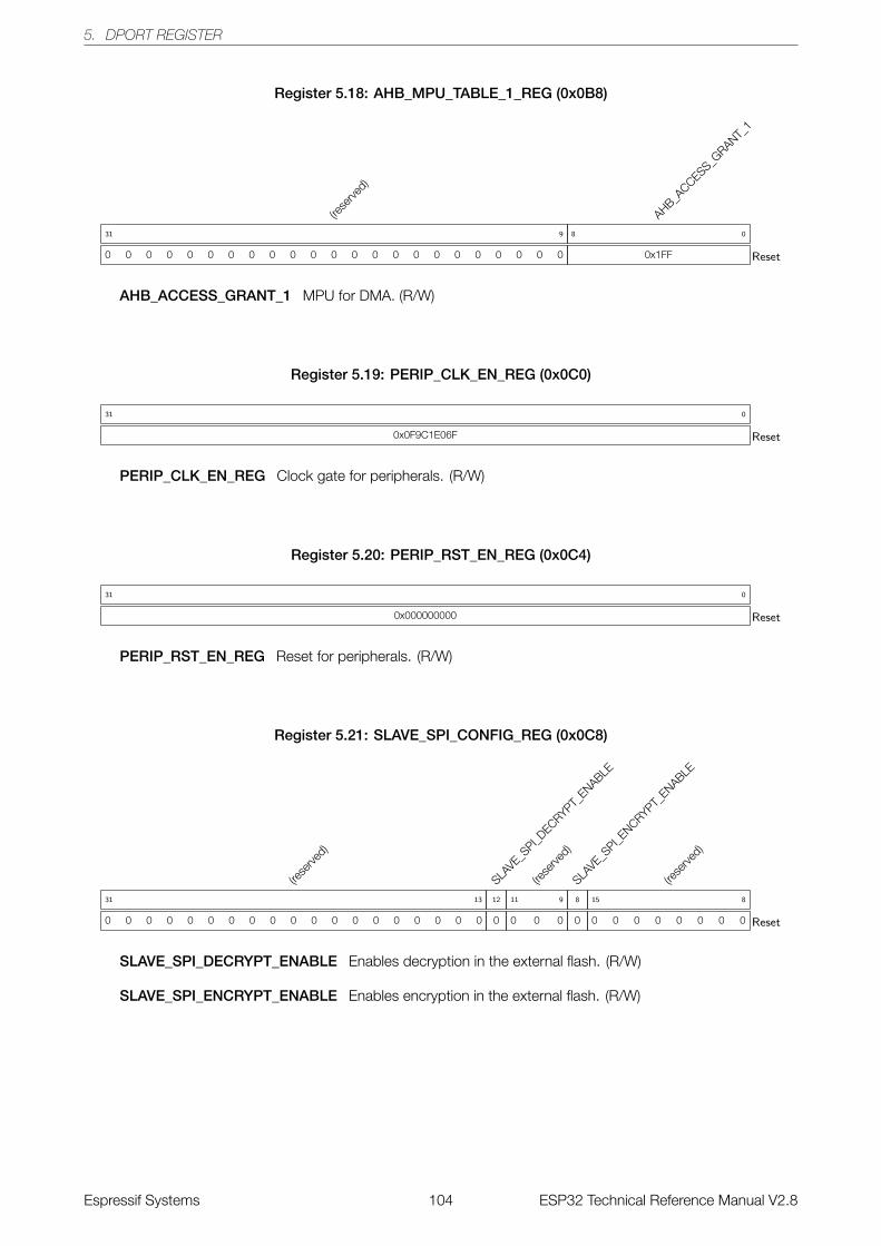
5. DPORT REGISTER
Register 5.18: AHB_MPU_TABLE_1_REG (0x0B8)
(rese
rved)
0 0 0 0 0 0 0 0 0 0 0 0 0 0 0 0 0 0 0 0 0 0 0
31 9
AHB_ACCESS_G
RANT_1
0x1FF
8 0
Reset
AHB_ACCESS_GRANT_1 MPU for DMA. (R/W)
Register 5.19: PERIP_CLK_EN_REG (0x0C0)
0x0F9C1E06F
31 0
Reset
PERIP_CLK_EN_REG Clock gate for peripherals. (R/W)
Register 5.20: PERIP_RST_EN_REG (0x0C4)
0x000000000
31 0
Reset
PERIP_RST_EN_REG Reset for peripherals. (R/W)
Register 5.21: SLAVE_SPI_CONFIG_REG (0x0C8)
(rese
rved)
0 0 0 0 0 0 0 0 0 0 0 0 0 0 0 0 0 0 0
31 13
SLAVE_S
PI_DECRYPT_
ENABLE
0
12
(rese
rved)
0 0 0
11 9
SLAVE_S
PI_ENCRYPT_
ENABLE
0
8
(rese
rved)
0 0 0 0 0 0 0 0
15 8
Reset
SLAVE_SPI_DECRYPT_ENABLE Enables decryption in the external flash. (R/W)
SLAVE_SPI_ENCRYPT_ENABLE Enables encryption in the external flash. (R/W)
Espressif Systems 104 ESP32 Technical Reference Manual V2.8
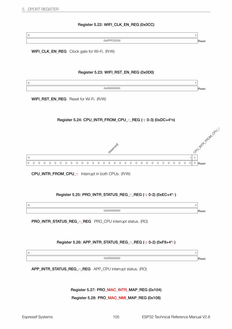
5. DPORT REGISTER
Register 5.22: WIFI_CLK_EN_REG (0x0CC)
0x0FFFCE030
31 0
Reset
WIFI_CLK_EN_REG Clock gate for Wi-Fi. (R/W)
Register 5.23: WIFI_RST_EN_REG (0x0D0)
0x000000000
31 0
Reset
WIFI_RST_EN_REG Reset for Wi-Fi. (R/W)
Register 5.24: CPU_INTR_FROM_CPU_n_REG (n: 0-3) (0xDC+4*n)
(rese
rved)
0 0 0 0 0 0 0 0 0 0 0 0 0 0 0 0 0 0 0 0 0 0 0 0 0 0 0 0 0 0 0
31 1
CPU_INTR
_FROM
_CPU_n
0
0
Reset
CPU_INTR_FROM_CPU_n Interrupt in both CPUs. (R/W)
Register 5.25: PRO_INTR_STATUS_REG_n_REG (n: 0-2) (0xEC+4*n)
0x000000000
31 0
Reset
PRO_INTR_STATUS_REG_n_REG PRO_CPU interrupt status. (RO)
Register 5.26: APP_INTR_STATUS_REG_n_REG (n: 0-2) (0xF8+4*n)
0x000000000
31 0
Reset
APP_INTR_STATUS_REG_n_REG APP_CPU interrupt status. (RO)
Register 5.27: PRO_MAC_INTR_MAP_REG (0x104)
Register 5.28: PRO_MAC_NMI_MAP_REG (0x108)
Espressif Systems 105 ESP32 Technical Reference Manual V2.8
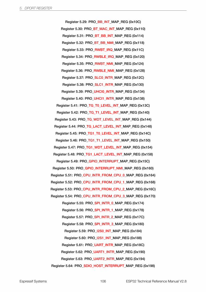
5. DPORT REGISTER
Register 5.29: PRO_BB_INT_MAP_REG (0x10C)
Register 5.30: PRO_BT_MAC_INT_MAP_REG (0x110)
Register 5.31: PRO_BT_BB_INT_MAP_REG (0x114)
Register 5.32: PRO_BT_BB_NMI_MAP_REG (0x118)
Register 5.33: PRO_RWBT_IRQ_MAP_REG (0x11C)
Register 5.34: PRO_RWBLE_IRQ_MAP_REG (0x120)
Register 5.35: PRO_RWBT_NMI_MAP_REG (0x124)
Register 5.36: PRO_RWBLE_NMI_MAP_REG (0x128)
Register 5.37: PRO_SLC0_INTR_MAP_REG (0x12C)
Register 5.38: PRO_SLC1_INTR_MAP_REG (0x130)
Register 5.39: PRO_UHCI0_INTR_MAP_REG (0x134)
Register 5.40: PRO_UHCI1_INTR_MAP_REG (0x138)
Register 5.41: PRO_TG_T0_LEVEL_INT_MAP_REG (0x13C)
Register 5.42: PRO_TG_T1_LEVEL_INT_MAP_REG (0x140)
Register 5.43: PRO_TG_WDT_LEVEL_INT_MAP_REG (0x144)
Register 5.44: PRO_TG_LACT_LEVEL_INT_MAP_REG (0x148)
Register 5.45: PRO_TG1_T0_LEVEL_INT_MAP_REG (0x14C)
Register 5.46: PRO_TG1_T1_LEVEL_INT_MAP_REG (0x150)
Register 5.47: PRO_TG1_WDT_LEVEL_INT_MAP_REG (0x154)
Register 5.48: PRO_TG1_LACT_LEVEL_INT_MAP_REG (0x158)
Register 5.49: PRO_GPIO_INTERRUPT_MAP_REG (0x15C)
Register 5.50: PRO_GPIO_INTERRUPT_NMI_MAP_REG (0x160)
Register 5.51: PRO_CPU_INTR_FROM_CPU_0_MAP_REG (0x164)
Register 5.52: PRO_CPU_INTR_FROM_CPU_1_MAP_REG (0x168)
Register 5.53: PRO_CPU_INTR_FROM_CPU_2_MAP_REG (0x16C)
Register 5.54: PRO_CPU_INTR_FROM_CPU_3_MAP_REG (0x170)
Register 5.55: PRO_SPI_INTR_0_MAP_REG (0x174)
Register 5.56: PRO_SPI_INTR_1_MAP_REG (0x178)
Register 5.57: PRO_SPI_INTR_2_MAP_REG (0x17C)
Register 5.58: PRO_SPI_INTR_3_MAP_REG (0x180)
Register 5.59: PRO_I2S0_INT_MAP_REG (0x184)
Register 5.60: PRO_I2S1_INT_MAP_REG (0x188)
Register 5.61: PRO_UART_INTR_MAP_REG (0x18C)
Register 5.62: PRO_UART1_INTR_MAP_REG (0x190)
Register 5.63: PRO_UART2_INTR_MAP_REG (0x194)
Register 5.64: PRO_SDIO_HOST_INTERRUPT_MAP_REG (0x198)
Espressif Systems 106 ESP32 Technical Reference Manual V2.8
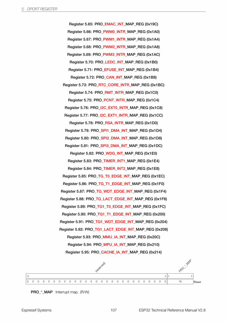
5. DPORT REGISTER
Register 5.65: PRO_EMAC_INT_MAP_REG (0x19C)
Register 5.66: PRO_PWM0_INTR_MAP_REG (0x1A0)
Register 5.67: PRO_PWM1_INTR_MAP_REG (0x1A4)
Register 5.68: PRO_PWM2_INTR_MAP_REG (0x1A8)
Register 5.69: PRO_PWM3_INTR_MAP_REG (0x1AC)
Register 5.70: PRO_LEDC_INT_MAP_REG (0x1B0)
Register 5.71: PRO_EFUSE_INT_MAP_REG (0x1B4)
Register 5.72: PRO_CAN_INT_MAP_REG (0x1B8)
Register 5.73: PRO_RTC_CORE_INTR_MAP_REG (0x1BC)
Register 5.74: PRO_RMT_INTR_MAP_REG (0x1C0)
Register 5.75: PRO_PCNT_INTR_MAP_REG (0x1C4)
Register 5.76: PRO_I2C_EXT0_INTR_MAP_REG (0x1C8)
Register 5.77: PRO_I2C_EXT1_INTR_MAP_REG (0x1CC)
Register 5.78: PRO_RSA_INTR_MAP_REG (0x1D0)
Register 5.79: PRO_SPI1_DMA_INT_MAP_REG (0x1D4)
Register 5.80: PRO_SPI2_DMA_INT_MAP_REG (0x1D8)
Register 5.81: PRO_SPI3_DMA_INT_MAP_REG (0x1DC)
Register 5.82: PRO_WDG_INT_MAP_REG (0x1E0)
Register 5.83: PRO_TIMER_INT1_MAP_REG (0x1E4)
Register 5.84: PRO_TIMER_INT2_MAP_REG (0x1E8)
Register 5.85: PRO_TG_T0_EDGE_INT_MAP_REG (0x1EC)
Register 5.86: PRO_TG_T1_EDGE_INT_MAP_REG (0x1F0)
Register 5.87: PRO_TG_WDT_EDGE_INT_MAP_REG (0x1F4)
Register 5.88: PRO_TG_LACT_EDGE_INT_MAP_REG (0x1F8)
Register 5.89: PRO_TG1_T0_EDGE_INT_MAP_REG (0x1FC)
Register 5.90: PRO_TG1_T1_EDGE_INT_MAP_REG (0x200)
Register 5.91: PRO_TG1_WDT_EDGE_INT_MAP_REG (0x204)
Register 5.92: PRO_TG1_LACT_EDGE_INT_MAP_REG (0x208)
Register 5.93: PRO_MMU_IA_INT_MAP_REG (0x20C)
Register 5.94: PRO_MPU_IA_INT_MAP_REG (0x210)
Register 5.95: PRO_CACHE_IA_INT_MAP_REG (0x214)
(rese
rved)
0 0 0 0 0 0 0 0 0 0 0 0 0 0 0 0 0 0 0 0 0 0 0 0 0 0 0
31 5
PRO_*_M
AP
16
4 0
Reset
PRO_*_MAP Interrupt map. (R/W)
Espressif Systems 107 ESP32 Technical Reference Manual V2.8
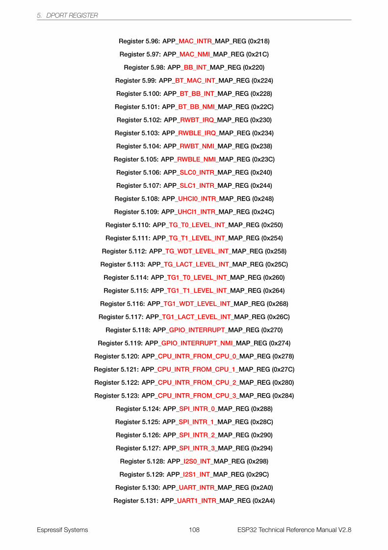
5. DPORT REGISTER
Register 5.96: APP_MAC_INTR_MAP_REG (0x218)
Register 5.97: APP_MAC_NMI_MAP_REG (0x21C)
Register 5.98: APP_BB_INT_MAP_REG (0x220)
Register 5.99: APP_BT_MAC_INT_MAP_REG (0x224)
Register 5.100: APP_BT_BB_INT_MAP_REG (0x228)
Register 5.101: APP_BT_BB_NMI_MAP_REG (0x22C)
Register 5.102: APP_RWBT_IRQ_MAP_REG (0x230)
Register 5.103: APP_RWBLE_IRQ_MAP_REG (0x234)
Register 5.104: APP_RWBT_NMI_MAP_REG (0x238)
Register 5.105: APP_RWBLE_NMI_MAP_REG (0x23C)
Register 5.106: APP_SLC0_INTR_MAP_REG (0x240)
Register 5.107: APP_SLC1_INTR_MAP_REG (0x244)
Register 5.108: APP_UHCI0_INTR_MAP_REG (0x248)
Register 5.109: APP_UHCI1_INTR_MAP_REG (0x24C)
Register 5.110: APP_TG_T0_LEVEL_INT_MAP_REG (0x250)
Register 5.111: APP_TG_T1_LEVEL_INT_MAP_REG (0x254)
Register 5.112: APP_TG_WDT_LEVEL_INT_MAP_REG (0x258)
Register 5.113: APP_TG_LACT_LEVEL_INT_MAP_REG (0x25C)
Register 5.114: APP_TG1_T0_LEVEL_INT_MAP_REG (0x260)
Register 5.115: APP_TG1_T1_LEVEL_INT_MAP_REG (0x264)
Register 5.116: APP_TG1_WDT_LEVEL_INT_MAP_REG (0x268)
Register 5.117: APP_TG1_LACT_LEVEL_INT_MAP_REG (0x26C)
Register 5.118: APP_GPIO_INTERRUPT_MAP_REG (0x270)
Register 5.119: APP_GPIO_INTERRUPT_NMI_MAP_REG (0x274)
Register 5.120: APP_CPU_INTR_FROM_CPU_0_MAP_REG (0x278)
Register 5.121: APP_CPU_INTR_FROM_CPU_1_MAP_REG (0x27C)
Register 5.122: APP_CPU_INTR_FROM_CPU_2_MAP_REG (0x280)
Register 5.123: APP_CPU_INTR_FROM_CPU_3_MAP_REG (0x284)
Register 5.124: APP_SPI_INTR_0_MAP_REG (0x288)
Register 5.125: APP_SPI_INTR_1_MAP_REG (0x28C)
Register 5.126: APP_SPI_INTR_2_MAP_REG (0x290)
Register 5.127: APP_SPI_INTR_3_MAP_REG (0x294)
Register 5.128: APP_I2S0_INT_MAP_REG (0x298)
Register 5.129: APP_I2S1_INT_MAP_REG (0x29C)
Register 5.130: APP_UART_INTR_MAP_REG (0x2A0)
Register 5.131: APP_UART1_INTR_MAP_REG (0x2A4)
Espressif Systems 108 ESP32 Technical Reference Manual V2.8
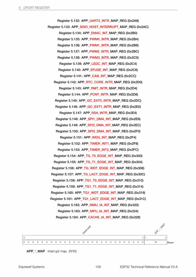
5. DPORT REGISTER
Register 5.132: APP_UART2_INTR_MAP_REG (0x2A8)
Register 5.133: APP_SDIO_HOST_INTERRUPT_MAP_REG (0x2AC)
Register 5.134: APP_EMAC_INT_MAP_REG (0x2B0)
Register 5.135: APP_PWM0_INTR_MAP_REG (0x2B4)
Register 5.136: APP_PWM1_INTR_MAP_REG (0x2B8)
Register 5.137: APP_PWM2_INTR_MAP_REG (0x2BC)
Register 5.138: APP_PWM3_INTR_MAP_REG (0x2C0)
Register 5.139: APP_LEDC_INT_MAP_REG (0x2C4)
Register 5.140: APP_EFUSE_INT_MAP_REG (0x2C8)
Register 5.141: APP_CAN_INT_MAP_REG (0x2CC)
Register 5.142: APP_RTC_CORE_INTR_MAP_REG (0x2D0)
Register 5.143: APP_RMT_INTR_MAP_REG (0x2D4)
Register 5.144: APP_PCNT_INTR_MAP_REG (0x2D8)
Register 5.145: APP_I2C_EXT0_INTR_MAP_REG (0x2DC)
Register 5.146: APP_I2C_EXT1_INTR_MAP_REG (0x2E0)
Register 5.147: APP_RSA_INTR_MAP_REG (0x2E4)
Register 5.148: APP_SPI1_DMA_INT_MAP_REG (0x2E8)
Register 5.149: APP_SPI2_DMA_INT_MAP_REG (0x2EC)
Register 5.150: APP_SPI3_DMA_INT_MAP_REG (0x2F0)
Register 5.151: APP_WDG_INT_MAP_REG (0x2F4)
Register 5.152: APP_TIMER_INT1_MAP_REG (0x2F8)
Register 5.153: APP_TIMER_INT2_MAP_REG (0x2FC)
Register 5.154: APP_TG_T0_EDGE_INT_MAP_REG (0x300)
Register 5.155: APP_TG_T1_EDGE_INT_MAP_REG (0x304)
Register 5.156: APP_TG_WDT_EDGE_INT_MAP_REG (0x308)
Register 5.157: APP_TG_LACT_EDGE_INT_MAP_REG (0x30C)
Register 5.158: APP_TG1_T0_EDGE_INT_MAP_REG (0x310)
Register 5.159: APP_TG1_T1_EDGE_INT_MAP_REG (0x314)
Register 5.160: APP_TG1_WDT_EDGE_INT_MAP_REG (0x318)
Register 5.161: APP_TG1_LACT_EDGE_INT_MAP_REG (0x31C)
Register 5.162: APP_MMU_IA_INT_MAP_REG (0x320)
Register 5.163: APP_MPU_IA_INT_MAP_REG (0x324)
Register 5.164: APP_CACHE_IA_INT_MAP_REG (0x328)
(rese
rved)
0 0 0 0 0 0 0 0 0 0 0 0 0 0 0 0 0 0 0 0 0 0 0 0 0 0 0
31 5
APP_*_M
AP
16
4 0
Reset
APP_*_MAP Interrupt map. (R/W)
Espressif Systems 109 ESP32 Technical Reference Manual V2.8
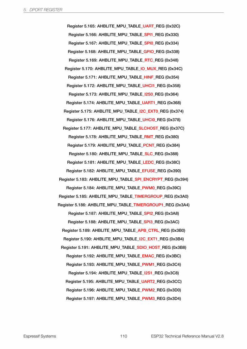
5. DPORT REGISTER
Register 5.165: AHBLITE_MPU_TABLE_UART_REG (0x32C)
Register 5.166: AHBLITE_MPU_TABLE_SPI1_REG (0x330)
Register 5.167: AHBLITE_MPU_TABLE_SPI0_REG (0x334)
Register 5.168: AHBLITE_MPU_TABLE_GPIO_REG (0x338)
Register 5.169: AHBLITE_MPU_TABLE_RTC_REG (0x348)
Register 5.170: AHBLITE_MPU_TABLE_IO_MUX_REG (0x34C)
Register 5.171: AHBLITE_MPU_TABLE_HINF_REG (0x354)
Register 5.172: AHBLITE_MPU_TABLE_UHCI1_REG (0x358)
Register 5.173: AHBLITE_MPU_TABLE_I2S0_REG (0x364)
Register 5.174: AHBLITE_MPU_TABLE_UART1_REG (0x368)
Register 5.175: AHBLITE_MPU_TABLE_I2C_EXT0_REG (0x374)
Register 5.176: AHBLITE_MPU_TABLE_UHCI0_REG (0x378)
Register 5.177: AHBLITE_MPU_TABLE_SLCHOST_REG (0x37C)
Register 5.178: AHBLITE_MPU_TABLE_RMT_REG (0x380)
Register 5.179: AHBLITE_MPU_TABLE_PCNT_REG (0x384)
Register 5.180: AHBLITE_MPU_TABLE_SLC_REG (0x388)
Register 5.181: AHBLITE_MPU_TABLE_LEDC_REG (0x38C)
Register 5.182: AHBLITE_MPU_TABLE_EFUSE_REG (0x390)
Register 5.183: AHBLITE_MPU_TABLE_SPI_ENCRYPT_REG (0x394)
Register 5.184: AHBLITE_MPU_TABLE_PWM0_REG (0x39C)
Register 5.185: AHBLITE_MPU_TABLE_TIMERGROUP_REG (0x3A0)
Register 5.186: AHBLITE_MPU_TABLE_TIMERGROUP1_REG (0x3A4)
Register 5.187: AHBLITE_MPU_TABLE_SPI2_REG (0x3A8)
Register 5.188: AHBLITE_MPU_TABLE_SPI3_REG (0x3AC)
Register 5.189: AHBLITE_MPU_TABLE_APB_CTRL_REG (0x3B0)
Register 5.190: AHBLITE_MPU_TABLE_I2C_EXT1_REG (0x3B4)
Register 5.191: AHBLITE_MPU_TABLE_SDIO_HOST_REG (0x3B8)
Register 5.192: AHBLITE_MPU_TABLE_EMAC_REG (0x3BC)
Register 5.193: AHBLITE_MPU_TABLE_PWM1_REG (0x3C4)
Register 5.194: AHBLITE_MPU_TABLE_I2S1_REG (0x3C8)
Register 5.195: AHBLITE_MPU_TABLE_UART2_REG (0x3CC)
Register 5.196: AHBLITE_MPU_TABLE_PWM2_REG (0x3D0)
Register 5.197: AHBLITE_MPU_TABLE_PWM3_REG (0x3D4)
Espressif Systems 110 ESP32 Technical Reference Manual V2.8
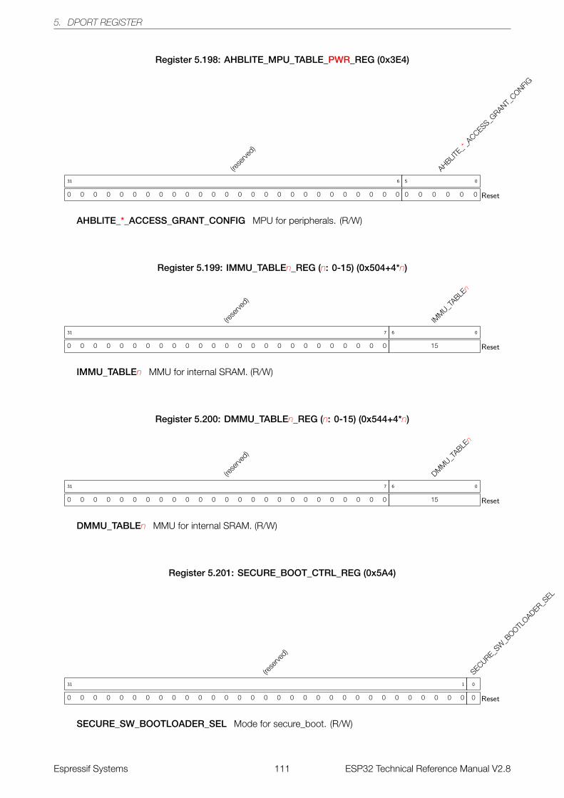
5. DPORT REGISTER
Register 5.198: AHBLITE_MPU_TABLE_PWR_REG (0x3E4)
(rese
rved)
0 0 0 0 0 0 0 0 0 0 0 0 0 0 0 0 0 0 0 0 0 0 0 0 0 0
31 6
AHBLITE_*
_ACCESS_G
RANT_CONFIG
0 0 0 0 0 0
5 0
Reset
AHBLITE_*_ACCESS_GRANT_CONFIG MPU for peripherals. (R/W)
Register 5.199: IMMU_TABLEn_REG (n: 0-15) (0x504+4*n)
(rese
rved)
0 0 0 0 0 0 0 0 0 0 0 0 0 0 0 0 0 0 0 0 0 0 0 0 0
31 7
IMM
U_TABLE
n
15
6 0
Reset
IMMU_TABLEn MMU for internal SRAM. (R/W)
Register 5.200: DMMU_TABLEn_REG (n: 0-15) (0x544+4*n)
(rese
rved)
0 0 0 0 0 0 0 0 0 0 0 0 0 0 0 0 0 0 0 0 0 0 0 0 0
31 7
DMM
U_TABLE
n
15
6 0
Reset
DMMU_TABLEn MMU for internal SRAM. (R/W)
Register 5.201: SECURE_BOOT_CTRL_REG (0x5A4)
(rese
rved)
0 0 0 0 0 0 0 0 0 0 0 0 0 0 0 0 0 0 0 0 0 0 0 0 0 0 0 0 0 0 0
31 1
SECURE_SW
_BOOTL
OADER_SEL
0
0
Reset
SECURE_SW_BOOTLOADER_SEL Mode for secure_boot. (R/W)
Espressif Systems 111 ESP32 Technical Reference Manual V2.8
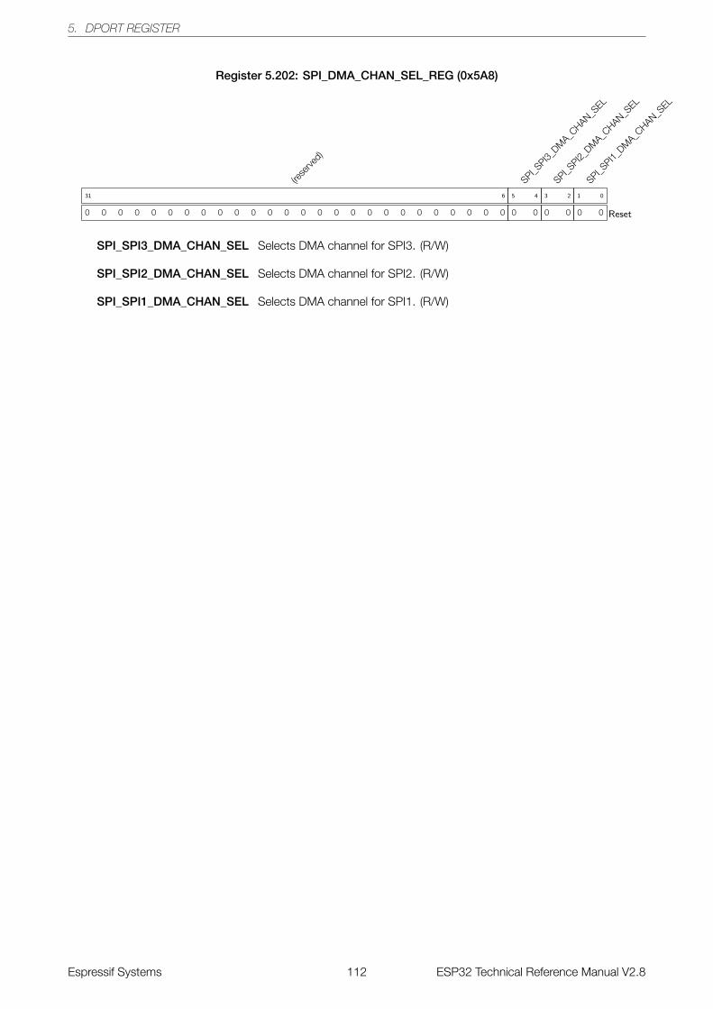
5. DPORT REGISTER
Register 5.202: SPI_DMA_CHAN_SEL_REG (0x5A8)
(rese
rved)
0 0 0 0 0 0 0 0 0 0 0 0 0 0 0 0 0 0 0 0 0 0 0 0 0 0
31 6
SPI_SPI3_
DMA_C
HAN_SEL
0 0
5 4
SPI_SPI2_
DMA_C
HAN_SEL
0 0
3 2
SPI_SPI1_
DMA_C
HAN_SEL
0 0
1 0
Reset
SPI_SPI3_DMA_CHAN_SEL Selects DMA channel for SPI3. (R/W)
SPI_SPI2_DMA_CHAN_SEL Selects DMA channel for SPI2. (R/W)
SPI_SPI1_DMA_CHAN_SEL Selects DMA channel for SPI1. (R/W)
Espressif Systems 112 ESP32 Technical Reference Manual V2.8
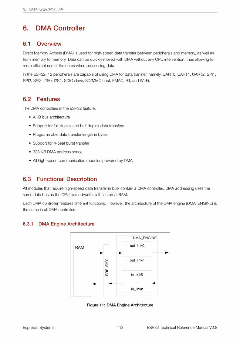
6. DMA CONTROLLER
6. DMA Controller
6.1 Overview
Direct Memory Access (DMA) is used for high-speed data transfer between peripherals and memory, as well as
from memory to memory. Data can be quickly moved with DMA without any CPU intervention, thus allowing for
more efficient use of the cores when processing data.
In the ESP32, 13 peripherals are capable of using DMA for data transfer, namely, UART0, UART1, UART2, SPI1,
SPI2, SPI3, I2S0, I2S1, SDIO slave, SD/MMC host, EMAC, BT, and Wi-Fi.
6.2 Features
The DMA controllers in the ESP32 feature:
• AHB bus architecture
• Support for full-duplex and half-duplex data transfers
• Programmable data transfer length in bytes
• Support for 4-beat burst transfer
• 328 KB DMA address space
• All high-speed communication modules powered by DMA
6.3 Functional Description
All modules that require high-speed data transfer in bulk contain a DMA controller. DMA addressing uses the
same data bus as the CPU to read/write to the internal RAM.
Each DMA controller features different functions. However, the architecture of the DMA engine (DMA_ENGINE) is
the same in all DMA controllers.
6.3.1 DMA Engine Architecture
Figure 11: DMA Engine Architecture
Espressif Systems 113 ESP32 Technical Reference Manual V2.8
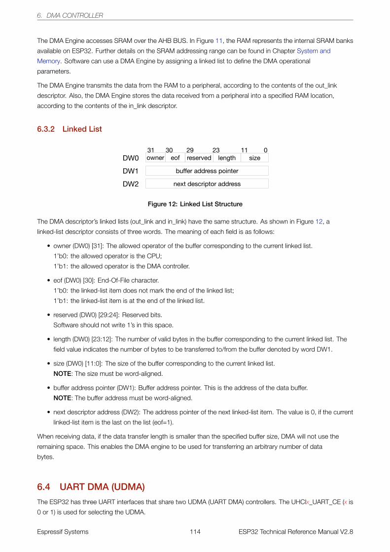
6. DMA CONTROLLER
The DMA Engine accesses SRAM over the AHB BUS. In Figure 11, the RAM represents the internal SRAM banks
available on ESP32. Further details on the SRAM addressing range can be found in Chapter System and
Memory. Software can use a DMA Engine by assigning a linked list to define the DMA operational
parameters.
The DMA Engine transmits the data from the RAM to a peripheral, according to the contents of the out_link
descriptor. Also, the DMA Engine stores the data received from a peripheral into a specified RAM location,
according to the contents of the in_link descriptor.
6.3.2 Linked List
Figure 12: Linked List Structure
The DMA descriptor’s linked lists (out_link and in_link) have the same structure. As shown in Figure 12, a
linked-list descriptor consists of three words. The meaning of each field is as follows:
• owner (DW0) [31]: The allowed operator of the buffer corresponding to the current linked list.
1’b0: the allowed operator is the CPU;
1’b1: the allowed operator is the DMA controller.
• eof (DW0) [30]: End-Of-File character.
1’b0: the linked-list item does not mark the end of the linked list;
1’b1: the linked-list item is at the end of the linked list.
• reserved (DW0) [29:24]: Reserved bits.
Software should not write 1’s in this space.
• length (DW0) [23:12]: The number of valid bytes in the buffer corresponding to the current linked list. The
field value indicates the number of bytes to be transferred to/from the buffer denoted by word DW1.
• size (DW0) [11:0]: The size of the buffer corresponding to the current linked list.
NOTE: The size must be word-aligned.
• buffer address pointer (DW1): Buffer address pointer. This is the address of the data buffer.
NOTE: The buffer address must be word-aligned.
• next descriptor address (DW2): The address pointer of the next linked-list item. The value is 0, if the current
linked-list item is the last on the list (eof=1).
When receiving data, if the data transfer length is smaller than the specified buffer size, DMA will not use the
remaining space. This enables the DMA engine to be used for transferring an arbitrary number of data
bytes.
6.4 UART DMA (UDMA)
The ESP32 has three UART interfaces that share two UDMA (UART DMA) controllers. The UHCIx_UART_CE (x is
0 or 1) is used for selecting the UDMA.
Espressif Systems 114 ESP32 Technical Reference Manual V2.8
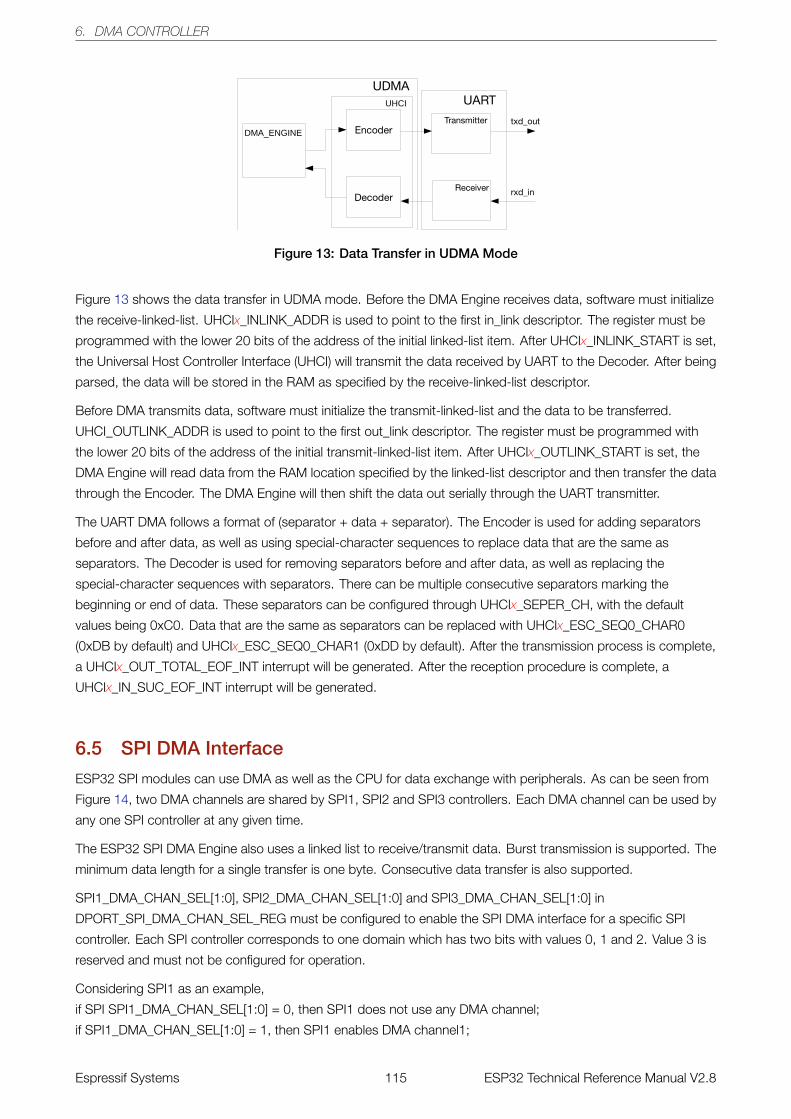
6. DMA CONTROLLER
Figure 13: Data Transfer in UDMA Mode
Figure 13 shows the data transfer in UDMA mode. Before the DMA Engine receives data, software must initialize
the receive-linked-list. UHCIx_INLINK_ADDR is used to point to the first in_link descriptor. The register must be
programmed with the lower 20 bits of the address of the initial linked-list item. After UHCIx_INLINK_START is set,
the Universal Host Controller Interface (UHCI) will transmit the data received by UART to the Decoder. After being
parsed, the data will be stored in the RAM as specified by the receive-linked-list descriptor.
Before DMA transmits data, software must initialize the transmit-linked-list and the data to be transferred.
UHCI_OUTLINK_ADDR is used to point to the first out_link descriptor. The register must be programmed with
the lower 20 bits of the address of the initial transmit-linked-list item. After UHCIx_OUTLINK_START is set, the
DMA Engine will read data from the RAM location specified by the linked-list descriptor and then transfer the data
through the Encoder. The DMA Engine will then shift the data out serially through the UART transmitter.
The UART DMA follows a format of (separator + data + separator). The Encoder is used for adding separators
before and after data, as well as using special-character sequences to replace data that are the same as
separators. The Decoder is used for removing separators before and after data, as well as replacing the
special-character sequences with separators. There can be multiple consecutive separators marking the
beginning or end of data. These separators can be configured through UHCIx_SEPER_CH, with the default
values being 0xC0. Data that are the same as separators can be replaced with UHCIx_ESC_SEQ0_CHAR0
(0xDB by default) and UHCIx_ESC_SEQ0_CHAR1 (0xDD by default). After the transmission process is complete,
a UHCIx_OUT_TOTAL_EOF_INT interrupt will be generated. After the reception procedure is complete, a
UHCIx_IN_SUC_EOF_INT interrupt will be generated.
6.5 SPI DMA Interface
ESP32 SPI modules can use DMA as well as the CPU for data exchange with peripherals. As can be seen from
Figure 14, two DMA channels are shared by SPI1, SPI2 and SPI3 controllers. Each DMA channel can be used by
any one SPI controller at any given time.
The ESP32 SPI DMA Engine also uses a linked list to receive/transmit data. Burst transmission is supported. The
minimum data length for a single transfer is one byte. Consecutive data transfer is also supported.
SPI1_DMA_CHAN_SEL[1:0], SPI2_DMA_CHAN_SEL[1:0] and SPI3_DMA_CHAN_SEL[1:0] in
DPORT_SPI_DMA_CHAN_SEL_REG must be configured to enable the SPI DMA interface for a specific SPI
controller. Each SPI controller corresponds to one domain which has two bits with values 0, 1 and 2. Value 3 is
reserved and must not be configured for operation.
Considering SPI1 as an example,
if SPI SPI1_DMA_CHAN_SEL[1:0] = 0, then SPI1 does not use any DMA channel;
if SPI1_DMA_CHAN_SEL[1:0] = 1, then SPI1 enables DMA channel1;
Espressif Systems 115 ESP32 Technical Reference Manual V2.8
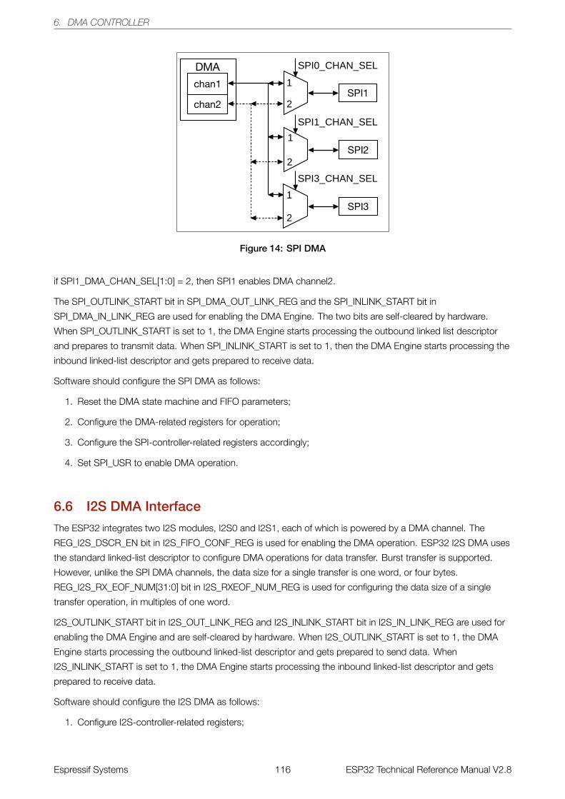
6. DMA CONTROLLER
Figure 14: SPI DMA
if SPI1_DMA_CHAN_SEL[1:0] = 2, then SPI1 enables DMA channel2.
The SPI_OUTLINK_START bit in SPI_DMA_OUT_LINK_REG and the SPI_INLINK_START bit in
SPI_DMA_IN_LINK_REG are used for enabling the DMA Engine. The two bits are self-cleared by hardware.
When SPI_OUTLINK_START is set to 1, the DMA Engine starts processing the outbound linked list descriptor
and prepares to transmit data. When SPI_INLINK_START is set to 1, then the DMA Engine starts processing the
inbound linked-list descriptor and gets prepared to receive data.
Software should configure the SPI DMA as follows:
1. Reset the DMA state machine and FIFO parameters;
2. Configure the DMA-related registers for operation;
3. Configure the SPI-controller-related registers accordingly;
4. Set SPI_USR to enable DMA operation.
6.6 I2S DMA Interface
The ESP32 integrates two I2S modules, I2S0 and I2S1, each of which is powered by a DMA channel. The
REG_I2S_DSCR_EN bit in I2S_FIFO_CONF_REG is used for enabling the DMA operation. ESP32 I2S DMA uses
the standard linked-list descriptor to configure DMA operations for data transfer. Burst transfer is supported.
However, unlike the SPI DMA channels, the data size for a single transfer is one word, or four bytes.
REG_I2S_RX_EOF_NUM[31:0] bit in I2S_RXEOF_NUM_REG is used for configuring the data size of a single
transfer operation, in multiples of one word.
I2S_OUTLINK_START bit in I2S_OUT_LINK_REG and I2S_INLINK_START bit in I2S_IN_LINK_REG are used for
enabling the DMA Engine and are self-cleared by hardware. When I2S_OUTLINK_START is set to 1, the DMA
Engine starts processing the outbound linked-list descriptor and gets prepared to send data. When
I2S_INLINK_START is set to 1, the DMA Engine starts processing the inbound linked-list descriptor and gets
prepared to receive data.
Software should configure the I2S DMA as follows:
1. Configure I2S-controller-related registers;
Espressif Systems 116 ESP32 Technical Reference Manual V2.8
6. DMA CONTROLLER
2. Reset the DMA state machine and FIFO parameters;
3. Configure DMA-related registers for operation;
4. In I2S master mode, set I2S_TX_START bit or I2S_RX_START bit to initiate an I2S operation;
In I2S slave mode, set I2S_TX_START bit or I2S_RX_START bit and wait for data transfer to be initiated by
the host device.
For more information on I2S DMA interrupts, please see Section DMA Interrupts, in Chapter I2S.
Espressif Systems 117 ESP32 Technical Reference Manual V2.8
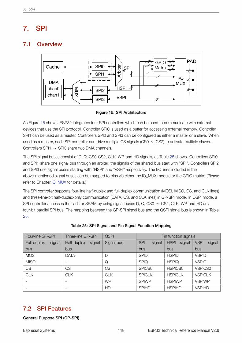
7. SPI
7. SPI
7.1 Overview
Figure 15: SPI Architecture
As Figure 15 shows, ESP32 integrates four SPI controllers which can be used to communicate with external
devices that use the SPI protocol. Controller SPI0 is used as a buffer for accessing external memory. Controller
SPI1 can be used as a master. Controllers SPI2 and SPI3 can be configured as either a master or a slave. When
used as a master, each SPI controller can drive multiple CS signals (CS0 ~ CS2) to activate multiple slaves.
Controllers SPI1 ~ SPI3 share two DMA channels.
The SPI signal buses consist of D, Q, CS0-CS2, CLK, WP, and HD signals, as Table 25 shows. Controllers SPI0
and SPI1 share one signal bus through an arbiter; the signals of the shared bus start with ”SPI”. Controllers SPI2
and SPI3 use signal buses starting with ”HSPI” and ”VSPI” respectively. The I/O lines included in the
above-mentioned signal buses can be mapped to pins via either the IO_MUX module or the GPIO matrix. (Please
refer to Chapter IO_MUX for details.)
The SPI controller supports four-line half-duplex and full-duplex communication (MOSI, MISO, CS, and CLK lines)
and three-line-bit half-duplex-only communication (DATA, CS, and CLK lines) in GP-SPI mode. In QSPI mode, a
SPI controller accesses the flash or SRAM by using signal buses D, Q, CS0 ~ CS2, CLK, WP, and HD as a
four-bit parallel SPI bus. The mapping between the GP-SPI signal bus and the QSPI signal bus is shown in Table
25.
Table 25: SPI Signal and Pin Signal Function Mapping
Four-line GP-SPI Three-line GP-SPI QSPI Pin function signals
Full-duplex signal
bus
Half-duplex signal
bus
Signal bus SPI signal
bus
HSPI signal
bus
VSPI signal
bus
MOSI DATA D SPID HSPID VSPID
MISO - Q SPIQ HSPIQ VSPIQ
CS CS CS SPICS0 HSPICS0 VSPICS0
CLK CLK CLK SPICLK HSPICLK VSPICLK
- - WP SPIWP HSPIWP VSPIWP
- - HD SPIHD HSPIHD VSPIHD
7.2 SPI Features
General Purpose SPI (GP-SPI)
Espressif Systems 118 ESP32 Technical Reference Manual V2.8
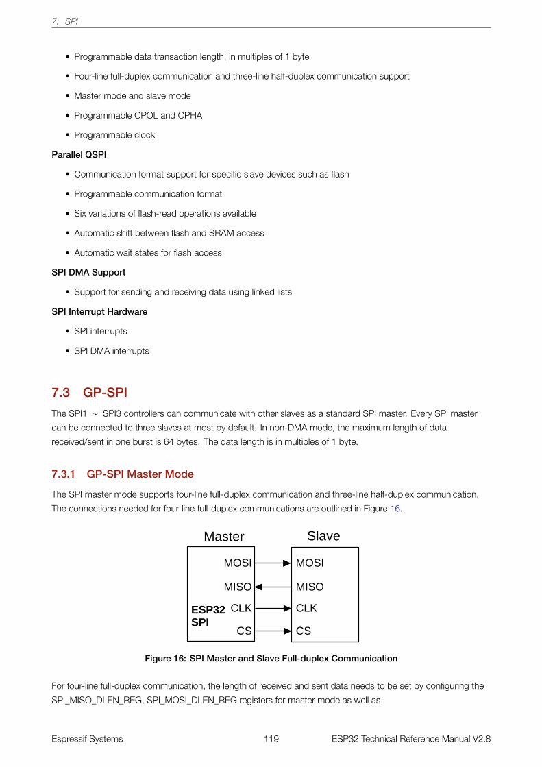
7. SPI
• Programmable data transaction length, in multiples of 1 byte
• Four-line full-duplex communication and three-line half-duplex communication support
• Master mode and slave mode
• Programmable CPOL and CPHA
• Programmable clock
Parallel QSPI
• Communication format support for specific slave devices such as flash
• Programmable communication format
• Six variations of flash-read operations available
• Automatic shift between flash and SRAM access
• Automatic wait states for flash access
SPI DMA Support
• Support for sending and receiving data using linked lists
SPI Interrupt Hardware
• SPI interrupts
• SPI DMA interrupts
7.3 GP-SPI
The SPI1 ~ SPI3 controllers can communicate with other slaves as a standard SPI master. Every SPI master
can be connected to three slaves at most by default. In non-DMA mode, the maximum length of data
received/sent in one burst is 64 bytes. The data length is in multiples of 1 byte.
7.3.1 GP-SPI Master Mode
The SPI master mode supports four-line full-duplex communication and three-line half-duplex communication.
The connections needed for four-line full-duplex communications are outlined in Figure 16.
Figure 16: SPI Master and Slave Full-duplex Communication
For four-line full-duplex communication, the length of received and sent data needs to be set by configuring the
SPI_MISO_DLEN_REG, SPI_MOSI_DLEN_REG registers for master mode as well as
Espressif Systems 119 ESP32 Technical Reference Manual V2.8
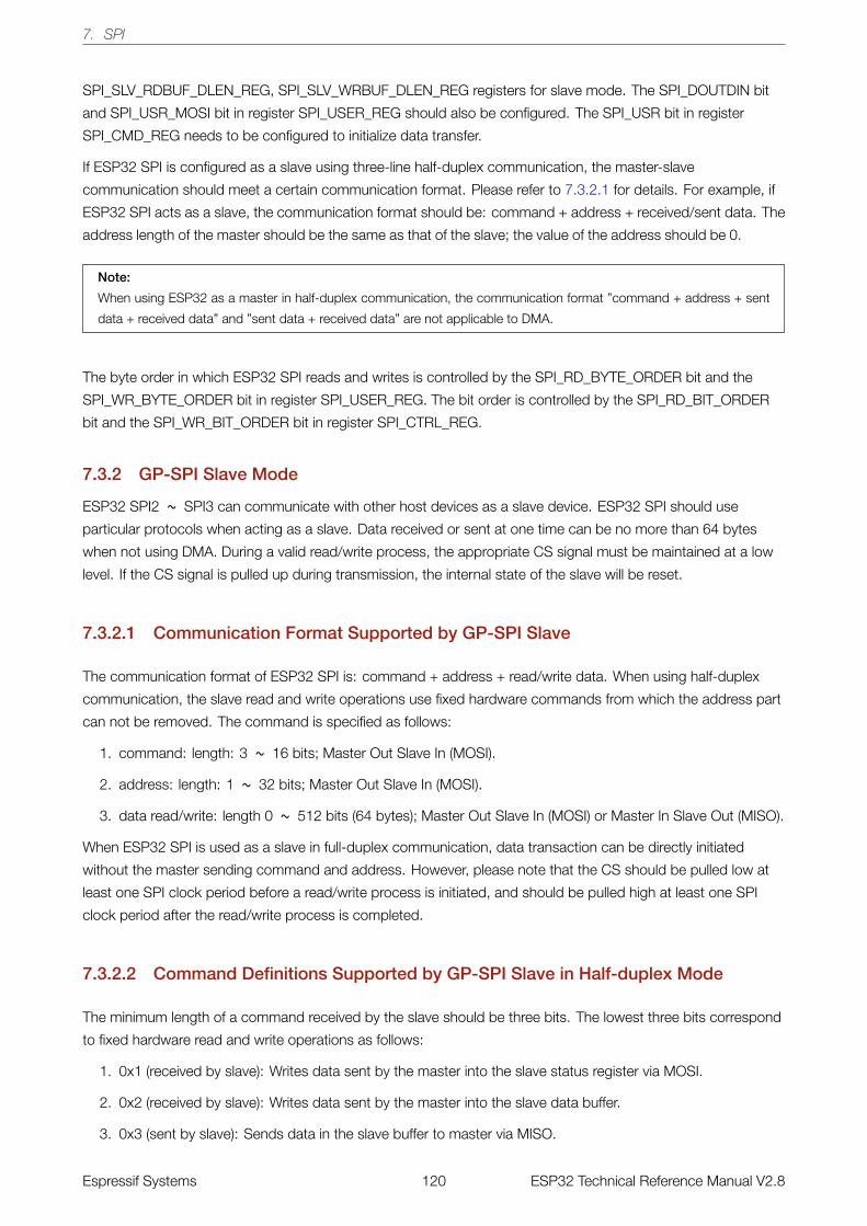
7. SPI
SPI_SLV_RDBUF_DLEN_REG, SPI_SLV_WRBUF_DLEN_REG registers for slave mode. The SPI_DOUTDIN bit
and SPI_USR_MOSI bit in register SPI_USER_REG should also be configured. The SPI_USR bit in register
SPI_CMD_REG needs to be configured to initialize data transfer.
If ESP32 SPI is configured as a slave using three-line half-duplex communication, the master-slave
communication should meet a certain communication format. Please refer to 7.3.2.1 for details. For example, if
ESP32 SPI acts as a slave, the communication format should be: command + address + received/sent data. The
address length of the master should be the same as that of the slave; the value of the address should be 0.
Note:
When using ESP32 as a master in half-duplex communication, the communication format ”command + address + sent
data + received data” and ”sent data + received data” are not applicable to DMA.
The byte order in which ESP32 SPI reads and writes is controlled by the SPI_RD_BYTE_ORDER bit and the
SPI_WR_BYTE_ORDER bit in register SPI_USER_REG. The bit order is controlled by the SPI_RD_BIT_ORDER
bit and the SPI_WR_BIT_ORDER bit in register SPI_CTRL_REG.
7.3.2 GP-SPI Slave Mode
ESP32 SPI2 ~ SPI3 can communicate with other host devices as a slave device. ESP32 SPI should use
particular protocols when acting as a slave. Data received or sent at one time can be no more than 64 bytes
when not using DMA. During a valid read/write process, the appropriate CS signal must be maintained at a low
level. If the CS signal is pulled up during transmission, the internal state of the slave will be reset.
7.3.2.1 Communication Format Supported by GP-SPI Slave
The communication format of ESP32 SPI is: command + address + read/write data. When using half-duplex
communication, the slave read and write operations use fixed hardware commands from which the address part
can not be removed. The command is specified as follows:
1. command: length: 3 ~ 16 bits; Master Out Slave In (MOSI).
2. address: length: 1 ~ 32 bits; Master Out Slave In (MOSI).
3. data read/write: length�0 ~ 512 bits (64 bytes); Master Out Slave In (MOSI) or Master In Slave Out (MISO).
When ESP32 SPI is used as a slave in full-duplex communication, data transaction can be directly initiated
without the master sending command and address. However, please note that the CS should be pulled low at
least one SPI clock period before a read/write process is initiated, and should be pulled high at least one SPI
clock period after the read/write process is completed.
7.3.2.2 Command Definitions Supported by GP-SPI Slave in Half-duplex Mode
The minimum length of a command received by the slave should be three bits. The lowest three bits correspond
to fixed hardware read and write operations as follows:
1. 0x1 (received by slave): Writes data sent by the master into the slave status register via MOSI.
2. 0x2 (received by slave): Writes data sent by the master into the slave data buffer.
3. 0x3 (sent by slave): Sends data in the slave buffer to master via MISO.
Espressif Systems 120 ESP32 Technical Reference Manual V2.8
7. SPI
4. 0x4 (sent by slave): Sends data in the slave status register to master via MISO.
5. 0x6 (received and then sent by slave): Writes master data on MOSI into data buffer and then sends the
date in the slave data buffer to MISO.
The master can write the slave status register SPI_SLV_WR_STATUS_REG, and decide whether to read data from
register SPI_SLV_WR_STATUS_REG or register SPI_RD_STATUS_REG via the SPI_SLV_STATUS_READBACK
bit in the register SPI_SLAVE1_REG. The SPI master can maintain communication with the slave by reading and
writing slave status register, thus realizing relatively complex communication with ease.
7.3.3 GP-SPI Data Buffer
Figure 17: SPI Data Buffer
ESP32 SPI has 16 x 32 bits of data buffer to buffer data-send and data-receive operations. As is shown in Figure
17, received data is written from the low byte of SPI_W0_REG by default and the writing ends with
SPI_W15_REG. If the data length is over 64 bytes, the extra part will be written from SPI_W0_REG.
Data buffer blocks SPI_W0_REG ~ SPI_W7_REG and SPI_W8_REG ~ SPI_W15_REG data correspond to the
lower part and the higher part respectively. They can be used separately, and are controlled by the
SPI_USR_MOSI_HIGHPART bit and the SPI_USR_MISO_HIGHPART bit in register SPI_USER_REG. For
example, if SPI is configured as a master, when SPI_USR_MOSI_HIGHPART = 1,
SPI_W8_REG ~ SPI_W15_REG are used as buffer for sending data; when SPI_USR_MISO_HIGHPART = 1,
SPI_W8_REG ~ SPI_W15_REG are used as buffer for receiving data. If SPI acts as a slave, when
SPI_USR_MOSI_HIGHPART = 1, SPI_W8_REG ~ SPI_W15_REG are used as buffer for receiving data; when
SPI_USR_MISO_HIGHPART = 1, SPI_W8_REG ~ SPI_W15_REG are used as buffer for sending data.
7.4 GP-SPI Clock Control
The maximum output clock frequency of ESP32 GP-SPI master is fapb/2, and the maximum input clock
frequency of the ESP32 GP-SPI slave is fapb/8. The master can derive other clock frequencies via frequency
division.
fspi =fapb
(SPI_CLKCNT_N+1)(SPI_CLKDIV_PRE+1)
SPI_CLKCNT_N and SPI_CLKDIV_PRE are two bits of register SPI_CLOCK_REG (Please refer to 7.8 Register
Description for details). When the SPI_CLK_EQU_SYSCLK bit in the register SPI_CLOCK_REG is set to 1, and
the other bits are set to 0, SPI output clock frequency is fapb. For other clock frequencies,
SPI_CLK_EQU_SYSCLK needs to be 0.
Espressif Systems 121 ESP32 Technical Reference Manual V2.8
7. SPI
7.4.1 GP-SPI Clock Polarity (CPOL) and Clock Phase (CPHA)
The clock polarity and clock phase of ESP32 SPI are controlled by the SPI_CK_IDLE_EDGE bit in register
SPI_PIN_REG, the SPI_CK_OUT_EDGE bit and the SPI_CK_I_EDGE bit in register SPI_USER_REG, the
SPI_MISO_DELAY_MODE[1:0] bit, the SPI_MISO_DELAY_NUM[2:0] bit, the SPI_MOSI_DELAY_MODE[1:0] bit,
and the SPI_MOSI_DELAY_MUM[2:0] bit in register SPI_CTRL2_REG. Table 26 and Table 27 show the clock
polarity and phase as well as the corresponding register values for ESP32 SPI master and slave,
respectively.
Table 26: Clock Polarity and Phase, and Corresponding SPI Register Values for SPI Master
Registers mode0 mode1 mode2 mode3
SPI_CK_IDLE_EDGE 0 0 1 1
SPI_CK_OUT_EDGE 0 1 1 0
SPI_MISO_DELAY_MODE 2(0) 1(0) 1(0) 2(0)
SPI_MISO_DELAY_NUM 0 0 0 0
SPI_MOSI_DELAY_MODE 0 0 0 0
SPI_MOSI_DELAY_NUM 0 0 0 0
Table 27: Clock Polarity and Phase, and Corresponding SPI Register Values for SPI Slave
Registers mode0 mode1 mode2 mode3
SPI_CK_IDLE_EDGE 0 0 1 1
SPI_CK_I_EDGE 0 1 1 0
SPI_MISO_DELAY_MODE 0 0 0 0
SPI_MISO_DELAY_NUM 0 0 0 0
SPI_MOSI_DELAY_MODE 2 1 1 2
SPI_MOSI_DELAY_NUM 0 0 0 0
1. mode0 means CPOL=0, CPHA=0. When SPI is idle, the clock output is logic low; data change on the
falling edge of the SPI clock and are sampled on the rising edge;
2. mode1 means CPOL=0, CPHA=1. When SPI is idle, the clock output is logic low; data change on the
rising edge of the SPI clock and are sampled on the falling edge;
3. mode2 means when CPOL=1, CPHA=0. When SPI is idle, the clock output is logic high; data change on
the rising edge of the SPI clock and are sampled on the falling edge;
4. mode3 means when CPOL=1, CPHA=1. When SPI is idle, the clock output is logic high; data change on
the falling edge of the SPI clock and are sampled on the rising edge.
7.4.2 GP-SPI Timing
The data signals of ESP32 GP-SPI can be mapped to physical pins via IO_MUX or via IO_MUX and GPIO matrix.
When signals pass through the matrix, they will be delayed by two clkapb clock cycles.
When GP-SPI is used as master and the data signals are not received by the SPI controller via GPIO matrix, if
GP-SPI output clock frequency is not higher than clkapb/2, register SPI_MISO_DELAY_MODE should be set to 0
when configuring the clock polarity. If GP-SPI output clock frequency is not higher than clkapb/4, register
Espressif Systems 122 ESP32 Technical Reference Manual V2.8
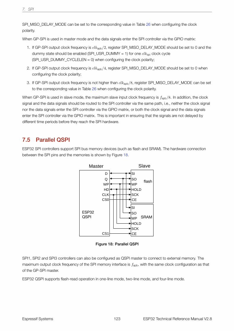
7. SPI
SPI_MISO_DELAY_MODE can be set to the corresponding value in Table 26 when configuring the clock
polarity.
When GP-SPI is used in master mode and the data signals enter the SPI controller via the GPIO matrix:
1. If GP-SPI output clock frequency is clkapb/2, register SPI_MISO_DELAY_MODE should be set to 0 and the
dummy state should be enabled (SPI_USR_DUMMY = 1) for one clkspi clock cycle
(SPI_USR_DUMMY_CYCLELEN = 0) when configuring the clock polarity;
2. If GP-SPI output clock frequency is clkapb/4, register SPI_MISO_DELAY_MODE should be set to 0 when
configuring the clock polarity;
3. If GP-SPI output clock frequency is not higher than clkapb/8, register SPI_MISO_DELAY_MODE can be set
to the corresponding value in Table 26 when configuring the clock polarity.
When GP-SPI is used in slave mode, the maximum slave input clock frequency is fapb/8. In addition, the clock
signal and the data signals should be routed to the SPI controller via the same path, i.e., neither the clock signal
nor the data signals enter the SPI controller via the GPIO matrix, or both the clock signal and the data signals
enter the SPI controller via the GPIO matrix. This is important in ensuring that the signals are not delayed by
different time periods before they reach the SPI hardware.
7.5 Parallel QSPI
ESP32 SPI controllers support SPI bus memory devices (such as flash and SRAM). The hardware connection
between the SPI pins and the memories is shown by Figure 18.
Figure 18: Parallel QSPI
SPI1, SPI2 and SPI3 controllers can also be configured as QSPI master to connect to external memory. The
maximum output clock frequency of the SPI memory interface is fapb, with the same clock configuration as that
of the GP-SPI master.
ESP32 QSPI supports flash-read operation in one-line mode, two-line mode, and four-line mode.
Espressif Systems 123 ESP32 Technical Reference Manual V2.8
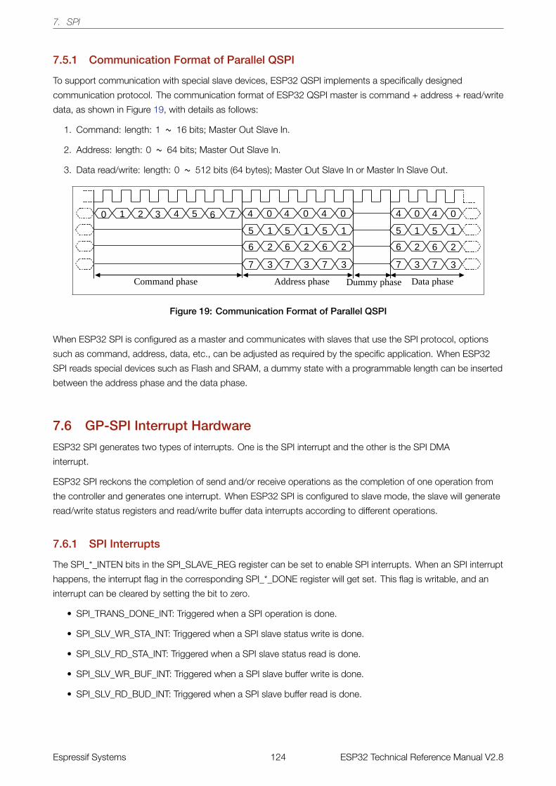
7. SPI
7.5.1 Communication Format of Parallel QSPI
To support communication with special slave devices, ESP32 QSPI implements a specifically designed
communication protocol. The communication format of ESP32 QSPI master is command + address + read/write
data, as shown in Figure 19, with details as follows:
1. Command: length: 1 ~ 16 bits; Master Out Slave In.
2. Address: length: 0 ~ 64 bits; Master Out Slave In.
3. Data read/write: length: 0 ~ 512 bits (64 bytes); Master Out Slave In or Master In Slave Out.
Figure 19: Communication Format of Parallel QSPI
When ESP32 SPI is configured as a master and communicates with slaves that use the SPI protocol, options
such as command, address, data, etc., can be adjusted as required by the specific application. When ESP32
SPI reads special devices such as Flash and SRAM, a dummy state with a programmable length can be inserted
between the address phase and the data phase.
7.6 GP-SPI Interrupt Hardware
ESP32 SPI generates two types of interrupts. One is the SPI interrupt and the other is the SPI DMA
interrupt.
ESP32 SPI reckons the completion of send and/or receive operations as the completion of one operation from
the controller and generates one interrupt. When ESP32 SPI is configured to slave mode, the slave will generate
read/write status registers and read/write buffer data interrupts according to different operations.
7.6.1 SPI Interrupts
The SPI_*_INTEN bits in the SPI_SLAVE_REG register can be set to enable SPI interrupts. When an SPI interrupt
happens, the interrupt flag in the corresponding SPI_*_DONE register will get set. This flag is writable, and an
interrupt can be cleared by setting the bit to zero.
• SPI_TRANS_DONE_INT: Triggered when a SPI operation is done.
• SPI_SLV_WR_STA_INT: Triggered when a SPI slave status write is done.
• SPI_SLV_RD_STA_INT: Triggered when a SPI slave status read is done.
• SPI_SLV_WR_BUF_INT: Triggered when a SPI slave buffer write is done.
• SPI_SLV_RD_BUD_INT: Triggered when a SPI slave buffer read is done.
Espressif Systems 124 ESP32 Technical Reference Manual V2.8
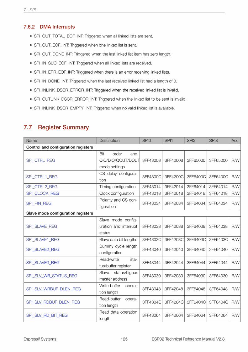
7. SPI
7.6.2 DMA Interrupts
• SPI_OUT_TOTAL_EOF_INT: Triggered when all linked lists are sent.
• SPI_OUT_EOF_INT: Triggered when one linked list is sent.
• SPI_OUT_DONE_INT: Triggered when the last linked list item has zero length.
• SPI_IN_SUC_EOF_INT: Triggered when all linked lists are received.
• SPI_IN_ERR_EOF_INT: Triggered when there is an error receiving linked lists.
• SPI_IN_DONE_INT: Triggered when the last received linked list had a length of 0.
• SPI_INLINK_DSCR_ERROR_INT: Triggered when the received linked list is invalid.
• SPI_OUTLINK_DSCR_ERROR_INT: Triggered when the linked list to be sent is invalid.
• SPI_INLINK_DSCR_EMPTY_INT: Triggered when no valid linked list is available.
7.7 Register Summary
Name Description SPI0 SPI1 SPI2 SPI3 Acc
Control and configuration registers
SPI_CTRL_REG
Bit order and
QIO/DIO/QOUT/DOUT
mode settings
3FF43008 3FF42008 3FF65000 3FF65000 R/W
SPI_CTRL1_REGCS delay configura-
tion3FF4300C 3FF4200C 3FF6400C 3FF6400C R/W
SPI_CTRL2_REG Timing configuration 3FF43014 3FF42014 3FF64014 3FF64014 R/W
SPI_CLOCK_REG Clock configuration 3FF43018 3FF42018 3FF64018 3FF64018 R/W
SPI_PIN_REGPolarity and CS con-
figuration3FF43034 3FF42034 3FF64034 3FF64034 R/W
Slave mode configuration registers
SPI_SLAVE_REG
Slave mode config-
uration and interrupt
status
3FF43038 3FF42038 3FF64038 3FF64038 R/W
SPI_SLAVE1_REG Slave data bit lengths 3FF4303C 3FF4203C 3FF6403C 3FF6403C R/W
SPI_SLAVE2_REGDummy cycle length
configuration3FF43040 3FF42040 3FF64040 3FF64040 R/W
SPI_SLAVE3_REGRead/write sta-
tus/buffer register3FF43044 3FF42044 3FF64044 3FF64044 R/W
SPI_SLV_WR_STATUS_REGSlave status/higher
master address3FF43030 3FF42030 3FF64030 3FF64030 R/W
SPI_SLV_WRBUF_DLEN_REGWrite-buffer opera-
tion length3FF43048 3FF42048 3FF64048 3FF64048 R/W
SPI_SLV_RDBUF_DLEN_REGRead-buffer opera-
tion length3FF4304C 3FF4204C 3FF6404C 3FF6404C R/W
SPI_SLV_RD_BIT_REGRead data operation
length3FF43064 3FF42064 3FF64064 3FF64064 R/W
Espressif Systems 125 ESP32 Technical Reference Manual V2.8
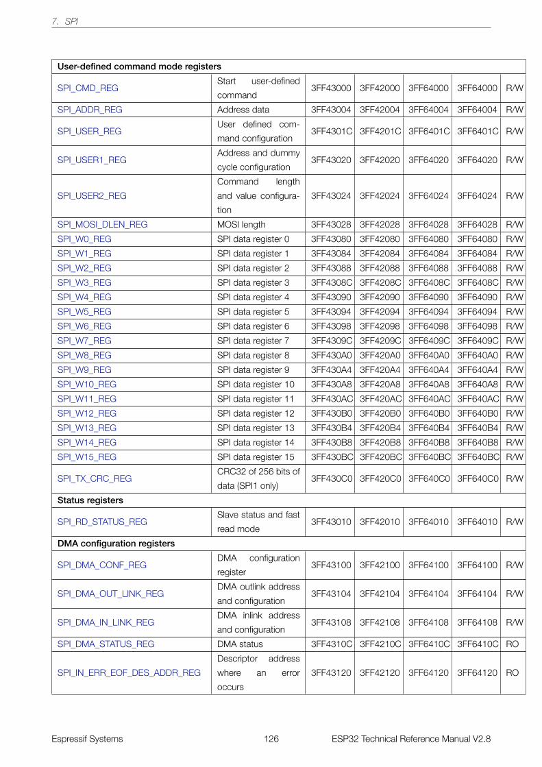
7. SPI
User-defined command mode registers
SPI_CMD_REGStart user-defined
command3FF43000 3FF42000 3FF64000 3FF64000 R/W
SPI_ADDR_REG Address data 3FF43004 3FF42004 3FF64004 3FF64004 R/W
SPI_USER_REGUser defined com-
mand configuration3FF4301C 3FF4201C 3FF6401C 3FF6401C R/W
SPI_USER1_REGAddress and dummy
cycle configuration3FF43020 3FF42020 3FF64020 3FF64020 R/W
SPI_USER2_REG
Command length
and value configura-
tion
3FF43024 3FF42024 3FF64024 3FF64024 R/W
SPI_MOSI_DLEN_REG MOSI length 3FF43028 3FF42028 3FF64028 3FF64028 R/W
SPI_W0_REG SPI data register 0 3FF43080 3FF42080 3FF64080 3FF64080 R/W
SPI_W1_REG SPI data register 1 3FF43084 3FF42084 3FF64084 3FF64084 R/W
SPI_W2_REG SPI data register 2 3FF43088 3FF42088 3FF64088 3FF64088 R/W
SPI_W3_REG SPI data register 3 3FF4308C 3FF4208C 3FF6408C 3FF6408C R/W
SPI_W4_REG SPI data register 4 3FF43090 3FF42090 3FF64090 3FF64090 R/W
SPI_W5_REG SPI data register 5 3FF43094 3FF42094 3FF64094 3FF64094 R/W
SPI_W6_REG SPI data register 6 3FF43098 3FF42098 3FF64098 3FF64098 R/W
SPI_W7_REG SPI data register 7 3FF4309C 3FF4209C 3FF6409C 3FF6409C R/W
SPI_W8_REG SPI data register 8 3FF430A0 3FF420A0 3FF640A0 3FF640A0 R/W
SPI_W9_REG SPI data register 9 3FF430A4 3FF420A4 3FF640A4 3FF640A4 R/W
SPI_W10_REG SPI data register 10 3FF430A8 3FF420A8 3FF640A8 3FF640A8 R/W
SPI_W11_REG SPI data register 11 3FF430AC 3FF420AC 3FF640AC 3FF640AC R/W
SPI_W12_REG SPI data register 12 3FF430B0 3FF420B0 3FF640B0 3FF640B0 R/W
SPI_W13_REG SPI data register 13 3FF430B4 3FF420B4 3FF640B4 3FF640B4 R/W
SPI_W14_REG SPI data register 14 3FF430B8 3FF420B8 3FF640B8 3FF640B8 R/W
SPI_W15_REG SPI data register 15 3FF430BC 3FF420BC 3FF640BC 3FF640BC R/W
SPI_TX_CRC_REGCRC32 of 256 bits of
data (SPI1 only)3FF430C0 3FF420C0 3FF640C0 3FF640C0 R/W
Status registers
SPI_RD_STATUS_REGSlave status and fast
read mode3FF43010 3FF42010 3FF64010 3FF64010 R/W
DMA configuration registers
SPI_DMA_CONF_REGDMA configuration
register3FF43100 3FF42100 3FF64100 3FF64100 R/W
SPI_DMA_OUT_LINK_REGDMA outlink address
and configuration3FF43104 3FF42104 3FF64104 3FF64104 R/W
SPI_DMA_IN_LINK_REGDMA inlink address
and configuration3FF43108 3FF42108 3FF64108 3FF64108 R/W
SPI_DMA_STATUS_REG DMA status 3FF4310C 3FF4210C 3FF6410C 3FF6410C RO
SPI_IN_ERR_EOF_DES_ADDR_REG
Descriptor address
where an error
occurs
3FF43120 3FF42120 3FF64120 3FF64120 RO
Espressif Systems 126 ESP32 Technical Reference Manual V2.8
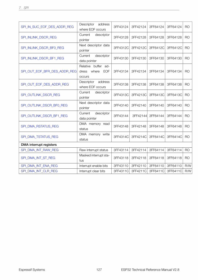
7. SPI
SPI_IN_SUC_EOF_DES_ADDR_REGDescriptor address
where EOF occurs3FF43124 3FF42124 3FF64124 3FF64124 RO
SPI_INLINK_DSCR_REGCurrent descriptor
pointer3FF43128 3FF42128 3FF64128 3FF64128 RO
SPI_INLINK_DSCR_BF0_REGNext descriptor data
pointer3FF4312C 3FF4212C 3FF6412C 3FF6412C RO
SPI_INLINK_DSCR_BF1_REGCurrent descriptor
data pointer3FF43130 3FF42130 3FF64130 3FF64130 RO
SPI_OUT_EOF_BFR_DES_ADDR_REG
Relative buffer ad-
dress where EOF
occurs
3FF43134 3FF42134 3FF64134 3FF64134 RO
SPI_OUT_EOF_DES_ADDR_REGDescriptor address
where EOF occurs3FF43138 3FF42138 3FF64138 3FF64138 RO
SPI_OUTLINK_DSCR_REGCurrent descriptor
pointer3FF4313C 3FF4213C 3FF6413C 3FF6413C RO
SPI_OUTLINK_DSCR_BF0_REGNext descriptor data
pointer3FF43140 3FF42140 3FF64140 3FF64140 RO
SPI_OUTLINK_DSCR_BF1_REGCurrent descriptor
data pointer3FF43144 3FF42144 3FF64144 3FF64144 RO
SPI_DMA_RSTATUS_REGDMA memory read
status3FF43148 3FF42148 3FF64148 3FF64148 RO
SPI_DMA_TSTATUS_REGDMA memory write
status3FF4314C 3FF4214C 3FF6414C 3FF6414C RO
DMA interrupt registers
SPI_DMA_INT_RAW_REG Raw interrupt status 3FF43114 3FF42114 3FF64114 3FF64114 RO
SPI_DMA_INT_ST_REGMasked interrupt sta-
tus3FF43118 3FF42118 3FF64118 3FF64118 RO
SPI_DMA_INT_ENA_REG Interrupt enable bits 3FF43110 3FF42110 3FF64110 3FF64110 R/W
SPI_DMA_INT_CLR_REG Interrupt clear bits 3FF4311C 3FF4211C 3FF6411C 3FF6411C R/W
Espressif Systems 127 ESP32 Technical Reference Manual V2.8
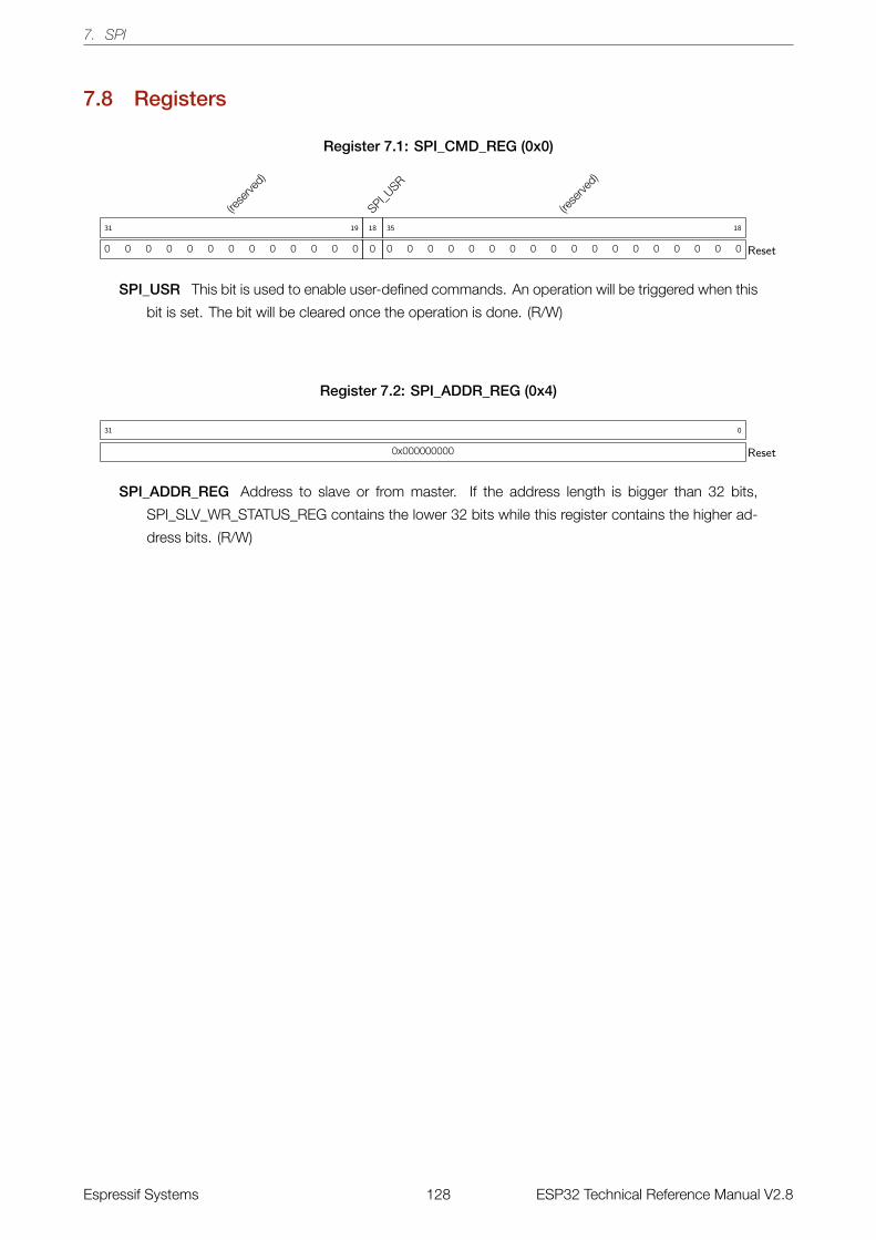
7. SPI
7.8 Registers
Register 7.1: SPI_CMD_REG (0x0)
(rese
rved)
0 0 0 0 0 0 0 0 0 0 0 0 0
31 19
SPI_USR
0
18
(rese
rved)
0 0 0 0 0 0 0 0 0 0 0 0 0 0 0 0 0 0
35 18
Reset
SPI_USR This bit is used to enable user-defined commands. An operation will be triggered when this
bit is set. The bit will be cleared once the operation is done. (R/W)
Register 7.2: SPI_ADDR_REG (0x4)
0x000000000
31 0
Reset
SPI_ADDR_REG Address to slave or from master. If the address length is bigger than 32 bits,
SPI_SLV_WR_STATUS_REG contains the lower 32 bits while this register contains the higher ad-
dress bits. (R/W)
Espressif Systems 128 ESP32 Technical Reference Manual V2.8
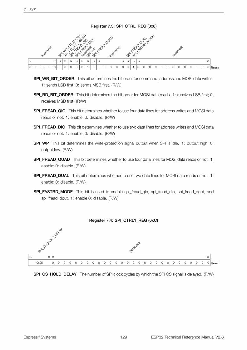
7. SPI
Register 7.3: SPI_CTRL_REG (0x8)
(rese
rved)
0 0 0 0 0
31 27
SPI_WR_B
IT_ORDER
0
26
SPI_RD_B
IT_ORDER
0
25
SPI_FREAD_Q
IO
0
24
SPI_FREAD_D
IO
0
23
(rese
rved)
0
22
SPI_WP
1
21
SPI_FREAD_Q
UAD
0
20
(rese
rved)
0 0 0 0 0
19 15
SPI_FREAD_D
UAL
0
14
SPI_FASTR
D_MODE
1
13
(rese
rved)
0 0 0 0 0 0 0 0 0 0 0 0 0
25 13
Reset
SPI_WR_BIT_ORDER This bit determines the bit order for command, address and MOSI data writes.
1: sends LSB first; 0: sends MSB first. (R/W)
SPI_RD_BIT_ORDER This bit determines the bit order for MOSI data reads. 1: receives LSB first; 0:
receives MSB first. (R/W)
SPI_FREAD_QIO This bit determines whether to use four data lines for address writes and MOSI data
reads or not. 1: enable; 0: disable. (R/W)
SPI_FREAD_DIO This bit determines whether to use two data lines for address writes and MOSI data
reads or not. 1: enable; 0: disable. (R/W)
SPI_WP This bit determines the write-protection signal output when SPI is idle. 1: output high; 0:
output low. (R/W)
SPI_FREAD_QUAD This bit determines whether to use four data lines for MOSI data reads or not. 1:
enable; 0: disable. (R/W)
SPI_FREAD_DUAL This bit determines whether to use two data lines for MOSI data reads or not. 1:
enable; 0: disable. (R/W)
SPI_FASTRD_MODE This bit is used to enable spi_fread_qio, spi_fread_dio, spi_fread_qout, and
spi_fread_dout. 1: enable�0: disable. (R/W)
Register 7.4: SPI_CTRL1_REG (0xC)
SPI_CS_H
OLD_D
ELAY
0x05
31 28
(rese
rved)
0 0 0 0 0 0 0 0 0 0 0 0 0 0 0 0 0 0 0 0 0 0 0 0 0 0 0 0
55 28
Reset
SPI_CS_HOLD_DELAY The number of SPI clock cycles by which the SPI CS signal is delayed. (R/W)
Espressif Systems 129 ESP32 Technical Reference Manual V2.8
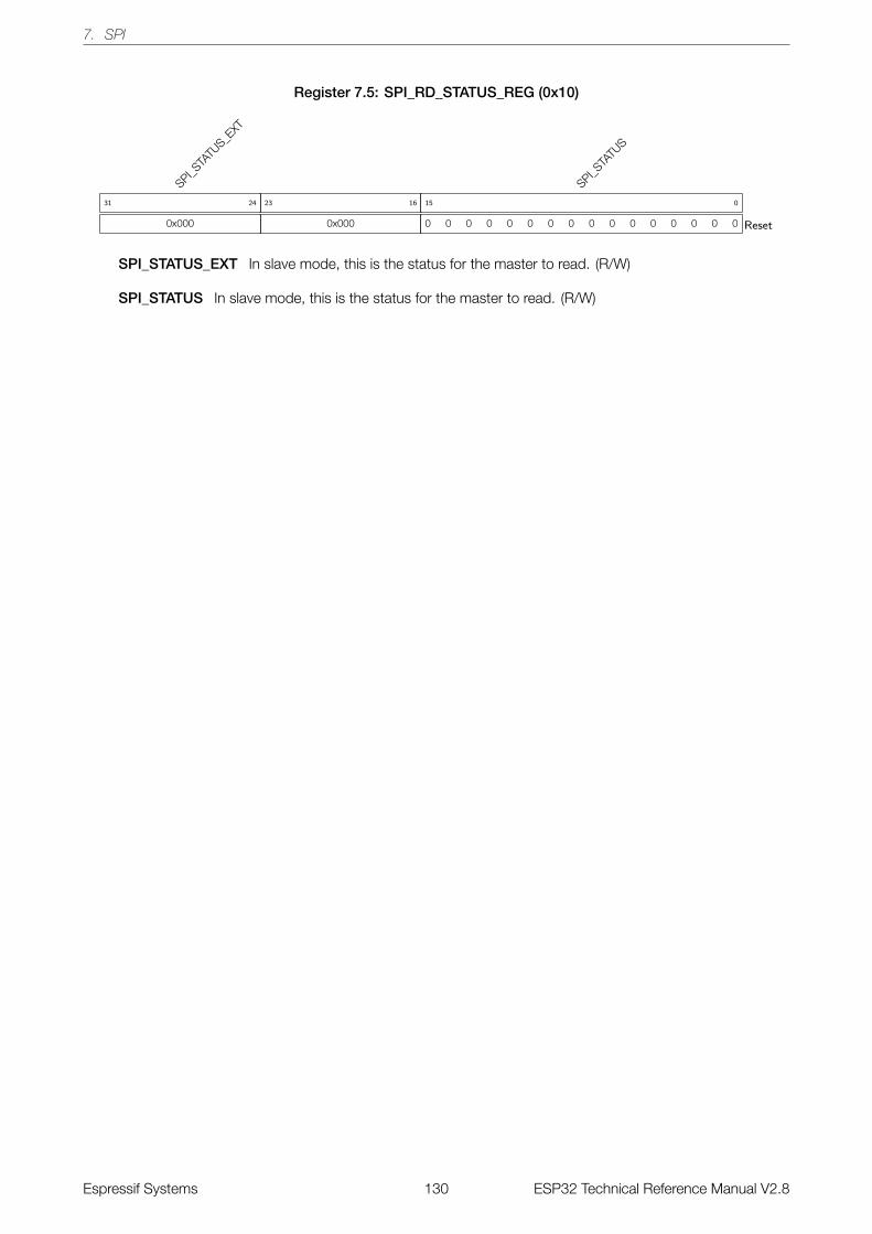
7. SPI
Register 7.5: SPI_RD_STATUS_REG (0x10)
SPI_STA
TUS_E
XT
0x000
31 24
0x000
23 16
SPI_STA
TUS
0 0 0 0 0 0 0 0 0 0 0 0 0 0 0 0
15 0
Reset
SPI_STATUS_EXT In slave mode, this is the status for the master to read. (R/W)
SPI_STATUS In slave mode, this is the status for the master to read. (R/W)
Espressif Systems 130 ESP32 Technical Reference Manual V2.8
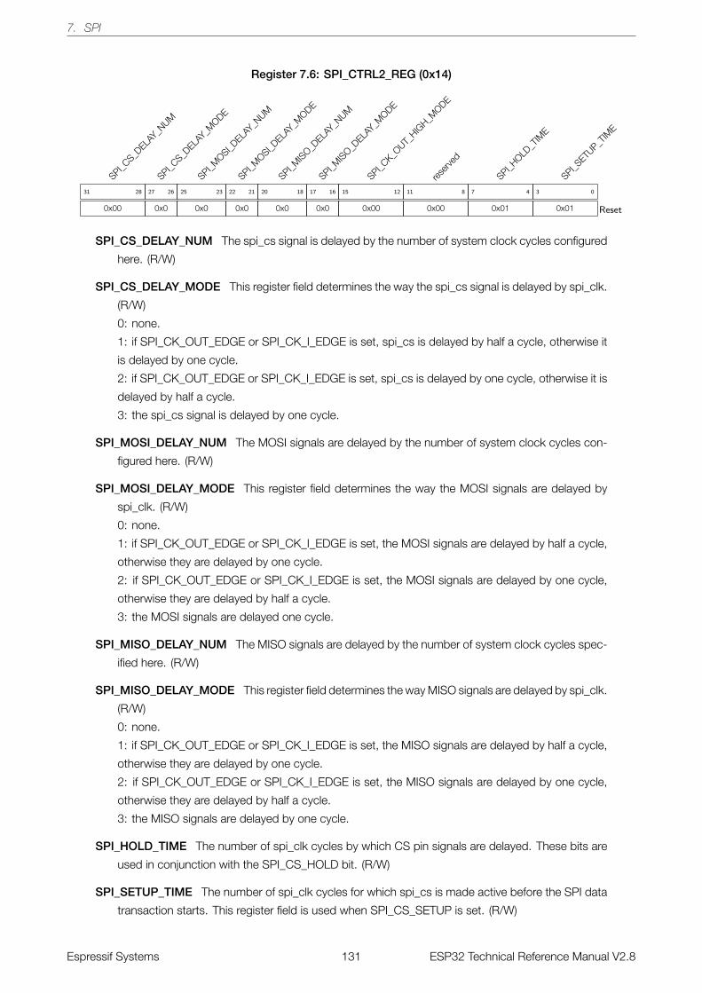
7. SPI
Register 7.6: SPI_CTRL2_REG (0x14)
SPI_CS_D
ELAY_N
UM
0x00
31 28
SPI_CS_D
ELAY_M
ODE
0x0
27 26
SPI_MOSI_D
ELAY_N
UM
0x0
25 23
SPI_MOSI_D
ELAY_M
ODE
0x0
22 21
SPI_MIS
O_DELA
Y_NUM
0x0
20 18
SPI_MIS
O_DELA
Y_MODE
0x0
17 16
SPI_CK_O
UT_HIG
H_MODE
0x00
15 12
reser
ved
0x00
11 8
SPI_HOLD
_TIM
E
0x01
7 4
SPI_SETU
P_TIM
E
0x01
3 0
Reset
SPI_CS_DELAY_NUM The spi_cs signal is delayed by the number of system clock cycles configured
here. (R/W)
SPI_CS_DELAY_MODE This register field determines the way the spi_cs signal is delayed by spi_clk.
(R/W)
0: none.
1: if SPI_CK_OUT_EDGE or SPI_CK_I_EDGE is set, spi_cs is delayed by half a cycle, otherwise it
is delayed by one cycle.
2: if SPI_CK_OUT_EDGE or SPI_CK_I_EDGE is set, spi_cs is delayed by one cycle, otherwise it is
delayed by half a cycle.
3: the spi_cs signal is delayed by one cycle.
SPI_MOSI_DELAY_NUM The MOSI signals are delayed by the number of system clock cycles con-
figured here. (R/W)
SPI_MOSI_DELAY_MODE This register field determines the way the MOSI signals are delayed by
spi_clk. (R/W)
0: none.
1: if SPI_CK_OUT_EDGE or SPI_CK_I_EDGE is set, the MOSI signals are delayed by half a cycle,
otherwise they are delayed by one cycle.
2: if SPI_CK_OUT_EDGE or SPI_CK_I_EDGE is set, the MOSI signals are delayed by one cycle,
otherwise they are delayed by half a cycle.
3: the MOSI signals are delayed one cycle.
SPI_MISO_DELAY_NUM The MISO signals are delayed by the number of system clock cycles spec-
ified here. (R/W)
SPI_MISO_DELAY_MODE This register field determines the way MISO signals are delayed by spi_clk.
(R/W)
0: none.
1: if SPI_CK_OUT_EDGE or SPI_CK_I_EDGE is set, the MISO signals are delayed by half a cycle,
otherwise they are delayed by one cycle.
2: if SPI_CK_OUT_EDGE or SPI_CK_I_EDGE is set, the MISO signals are delayed by one cycle,
otherwise they are delayed by half a cycle.
3: the MISO signals are delayed by one cycle.
SPI_HOLD_TIME The number of spi_clk cycles by which CS pin signals are delayed. These bits are
used in conjunction with the SPI_CS_HOLD bit. (R/W)
SPI_SETUP_TIME The number of spi_clk cycles for which spi_cs is made active before the SPI data
transaction starts. This register field is used when SPI_CS_SETUP is set. (R/W)
Espressif Systems 131 ESP32 Technical Reference Manual V2.8
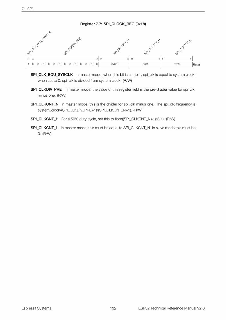
7. SPI
Register 7.7: SPI_CLOCK_REG (0x18)
SPI_CLK
_EQU_S
YSCLK
1
31
SPI_CLK
DIV_PRE
0 0 0 0 0 0 0 0 0 0 0 0 0
30 18
SPI_CLK
CNT_N
0x03
17 12
SPI_CLK
CNT_H
0x01
11 6
SPI_CLK
CNT_L
0x03
5 0
Reset
SPI_CLK_EQU_SYSCLK In master mode, when this bit is set to 1, spi_clk is equal to system clock;
when set to 0, spi_clk is divided from system clock. (R/W)
SPI_CLKDIV_PRE In master mode, the value of this register field is the pre-divider value for spi_clk,
minus one. (R/W)
SPI_CLKCNT_N In master mode, this is the divider for spi_clk minus one. The spi_clk frequency is
system_clock/(SPI_CLKDIV_PRE+1)/(SPI_CLKCNT_N+1). (R/W)
SPI_CLKCNT_H For a 50% duty cycle, set this to floor((SPI_CLKCNT_N+1)/2-1). (R/W)
SPI_CLKCNT_L In master mode, this must be equal to SPI_CLKCNT_N. In slave mode this must be
0. (R/W)
Espressif Systems 132 ESP32 Technical Reference Manual V2.8
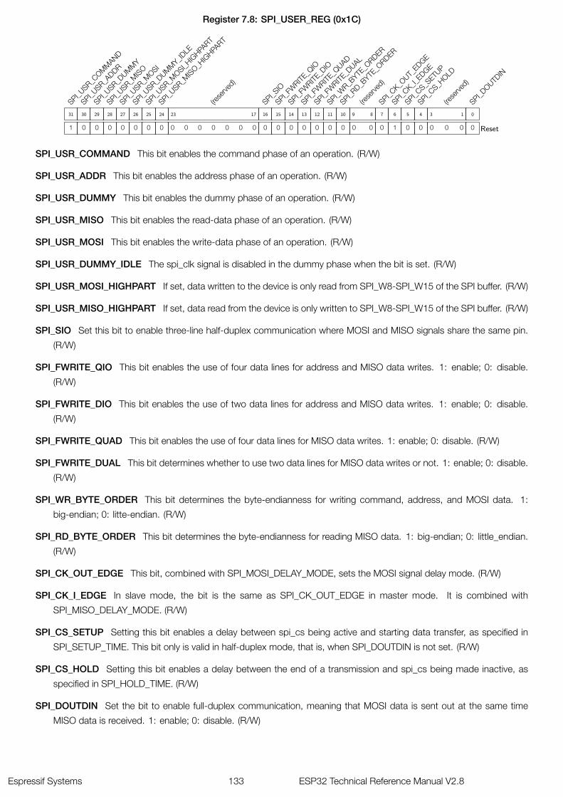
7. SPI
Register 7.8: SPI_USER_REG (0x1C)
SPI_USR_C
OMM
AND
1
31
SPI_USR_A
DDR
0
30
SPI_USR_D
UMM
Y
0
29
SPI_USR_M
ISO
0
28
SPI_USR_M
OSI
0
27
SPI_USR_D
UMM
Y_IDLE
0
26
SPI_USR_M
OSI_HIG
HPART
0
25
SPI_USR_M
ISO_H
IGHPA
RT
0
24
(rese
rved)
0 0 0 0 0 0 0
23 17
SPI_SIO
0
16
SPI_FW
RITE_Q
IO
0
15
SPI_FW
RITE_D
IO
0
14
SPI_FW
RITE_Q
UAD
0
13
SPI_FW
RITE_D
UAL
0
12
SPI_WR_B
YTE_O
RDER
0
11
SPI_RD_B
YTE_O
RDER
0
10
(rese
rved)
0 0
9 8
SPI_CK_O
UT_EDGE
0
7
SPI_CK_I_
EDGE
1
6
SPI_CS_S
ETUP
0
5
SPI_CS_H
OLD
0
4
(rese
rved)
0 0 0
3 1
SPI_DOUTD
IN
0
0
Reset
SPI_USR_COMMAND This bit enables the command phase of an operation. (R/W)
SPI_USR_ADDR This bit enables the address phase of an operation. (R/W)
SPI_USR_DUMMY This bit enables the dummy phase of an operation. (R/W)
SPI_USR_MISO This bit enables the read-data phase of an operation. (R/W)
SPI_USR_MOSI This bit enables the write-data phase of an operation. (R/W)
SPI_USR_DUMMY_IDLE The spi_clk signal is disabled in the dummy phase when the bit is set. (R/W)
SPI_USR_MOSI_HIGHPART If set, data written to the device is only read from SPI_W8-SPI_W15 of the SPI buffer. (R/W)
SPI_USR_MISO_HIGHPART If set, data read from the device is only written to SPI_W8-SPI_W15 of the SPI buffer. (R/W)
SPI_SIO Set this bit to enable three-line half-duplex communication where MOSI and MISO signals share the same pin.
(R/W)
SPI_FWRITE_QIO This bit enables the use of four data lines for address and MISO data writes. 1: enable; 0: disable.
(R/W)
SPI_FWRITE_DIO This bit enables the use of two data lines for address and MISO data writes. 1: enable; 0: disable.
(R/W)
SPI_FWRITE_QUAD This bit enables the use of four data lines for MISO data writes. 1: enable; 0: disable. (R/W)
SPI_FWRITE_DUAL This bit determines whether to use two data lines for MISO data writes or not. 1: enable; 0: disable.
(R/W)
SPI_WR_BYTE_ORDER This bit determines the byte-endianness for writing command, address, and MOSI data. 1:
big-endian; 0: litte-endian. (R/W)
SPI_RD_BYTE_ORDER This bit determines the byte-endianness for reading MISO data. 1: big-endian; 0: little_endian.
(R/W)
SPI_CK_OUT_EDGE This bit, combined with SPI_MOSI_DELAY_MODE, sets the MOSI signal delay mode. (R/W)
SPI_CK_I_EDGE In slave mode, the bit is the same as SPI_CK_OUT_EDGE in master mode. It is combined with
SPI_MISO_DELAY_MODE. (R/W)
SPI_CS_SETUP Setting this bit enables a delay between spi_cs being active and starting data transfer, as specified in
SPI_SETUP_TIME. This bit only is valid in half-duplex mode, that is, when SPI_DOUTDIN is not set. (R/W)
SPI_CS_HOLD Setting this bit enables a delay between the end of a transmission and spi_cs being made inactive, as
specified in SPI_HOLD_TIME. (R/W)
SPI_DOUTDIN Set the bit to enable full-duplex communication, meaning that MOSI data is sent out at the same time
MISO data is received. 1: enable; 0: disable. (R/W)
Espressif Systems 133 ESP32 Technical Reference Manual V2.8
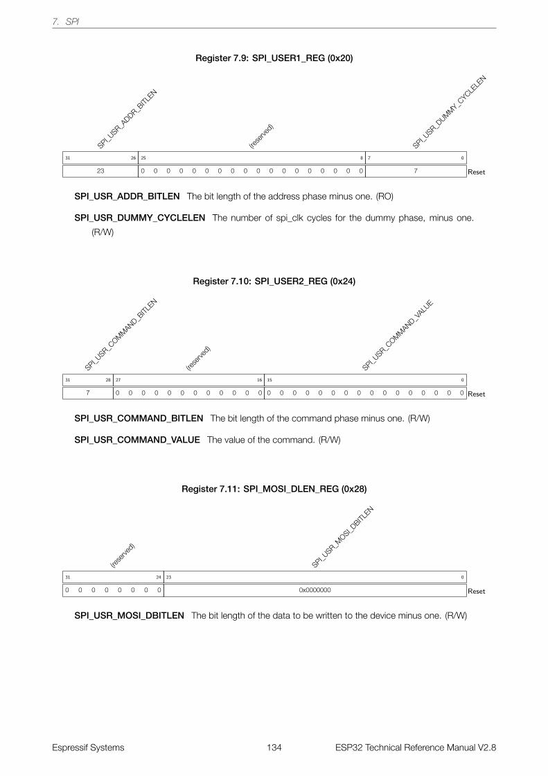
7. SPI
Register 7.9: SPI_USER1_REG (0x20)
SPI_USR_A
DDR_BITL
EN
23
31 26
(rese
rved)
0 0 0 0 0 0 0 0 0 0 0 0 0 0 0 0 0 0
25 8
SPI_USR_D
UMM
Y_CYCLE
LEN
7
7 0
Reset
SPI_USR_ADDR_BITLEN The bit length of the address phase minus one. (RO)
SPI_USR_DUMMY_CYCLELEN The number of spi_clk cycles for the dummy phase, minus one.
(R/W)
Register 7.10: SPI_USER2_REG (0x24)
SPI_USR_C
OMM
AND_BITL
EN
7
31 28
(rese
rved)
0 0 0 0 0 0 0 0 0 0 0 0
27 16
SPI_USR_C
OMM
AND_VALU
E
0 0 0 0 0 0 0 0 0 0 0 0 0 0 0 0
15 0
Reset
SPI_USR_COMMAND_BITLEN The bit length of the command phase minus one. (R/W)
SPI_USR_COMMAND_VALUE The value of the command. (R/W)
Register 7.11: SPI_MOSI_DLEN_REG (0x28)
(rese
rved)
0 0 0 0 0 0 0 0
31 24
SPI_USR_M
OSI_DBITL
EN
0x0000000
23 0
Reset
SPI_USR_MOSI_DBITLEN The bit length of the data to be written to the device minus one. (R/W)
Espressif Systems 134 ESP32 Technical Reference Manual V2.8

7. SPI
Register 7.12: SPI_MISO_DLEN_REG (0x2C)
(rese
rved)
0 0 0 0 0 0 0 0
31 24
SPI_USR_M
ISO_D
BITLEN
0x0000000
23 0
Reset
SPI_USR_MISO_DBITLEN The bit length of the data to be read from the device, minus one. (R/W)
Register 7.13: SPI_SLV_WR_STATUS_REG (0x30)
0 0 0 0 0 0 0 0 0 0 0 0 0 0 0 0 0 0 0 0 0 0 0 0 0 0 0 0 0 0 0 0
31 0
Reset
SPI_SLV_WR_STATUS_REG In the slave mode this register is the status register for the master to
write into. In the master mode, if the address length is bigger than 32 bits, this register contains
the lower 32 bits. (R/W)
Espressif Systems 135 ESP32 Technical Reference Manual V2.8
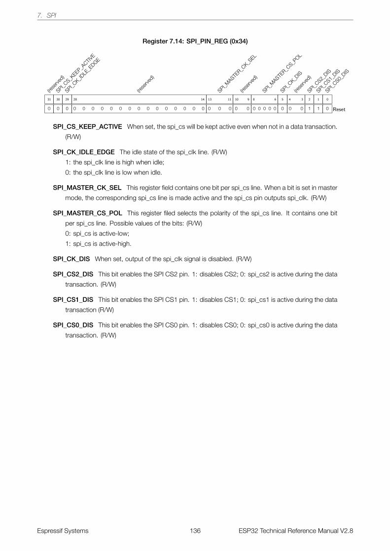
7. SPI
Register 7.14: SPI_PIN_REG (0x34)
(rese
rved)
0
31
SPI_CS_K
EEP_ACTIV
E
0
30
SPI_CK_ID
LE_E
DGE
0
29
(rese
rved)
0 0 0 0 0 0 0 0 0 0 0 0 0 0 0
28 14
SPI_MASTE
R_CK_S
EL
0 0 0
13 11
(rese
rved)
0 0
10 9
SPI_MASTE
R_CS_P
OL
0 0 0 0 0
8 6
SPI_CK_D
IS
0
5
(rese
rved)
0 0
4 3
SPI_CS2_
DIS
1
2
SPI_CS1_
DIS
1
1
SPI_CS0_
DIS
0
0
Reset
SPI_CS_KEEP_ACTIVE When set, the spi_cs will be kept active even when not in a data transaction.
(R/W)
SPI_CK_IDLE_EDGE The idle state of the spi_clk line. (R/W)
1: the spi_clk line is high when idle;
0: the spi_clk line is low when idle.
SPI_MASTER_CK_SEL This register field contains one bit per spi_cs line. When a bit is set in master
mode, the corresponding spi_cs line is made active and the spi_cs pin outputs spi_clk. (R/W)
SPI_MASTER_CS_POL This register filed selects the polarity of the spi_cs line. It contains one bit
per spi_cs line. Possible values of the bits: (R/W)
0: spi_cs is active-low;
1: spi_cs is active-high.
SPI_CK_DIS When set, output of the spi_clk signal is disabled. (R/W)
SPI_CS2_DIS This bit enables the SPI CS2 pin. 1: disables CS2; 0: spi_cs2 is active during the data
transaction. (R/W)
SPI_CS1_DIS This bit enables the SPI CS1 pin. 1: disables CS1; 0: spi_cs1 is active during the data
transaction (R/W)
SPI_CS0_DIS This bit enables the SPI CS0 pin. 1: disables CS0; 0: spi_cs0 is active during the data
transaction. (R/W)
Espressif Systems 136 ESP32 Technical Reference Manual V2.8
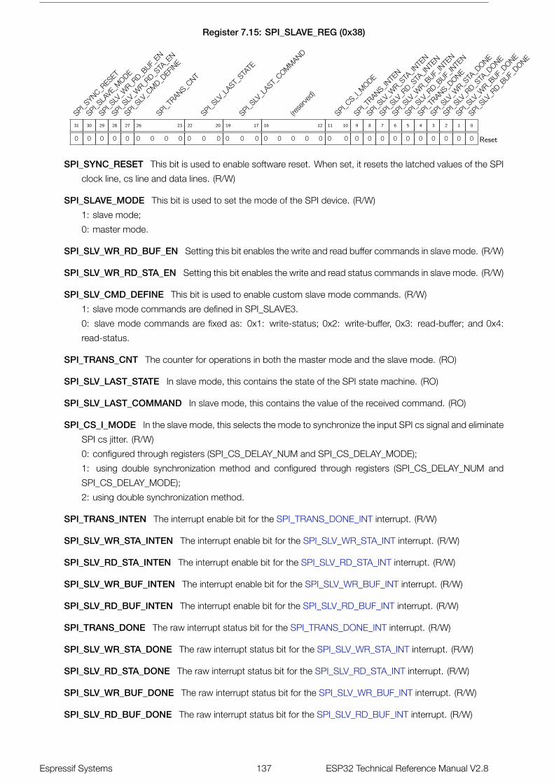
7. SPI
Register 7.15: SPI_SLAVE_REG (0x38)
SPI_SYNC_R
ESET
0
31
SPI_SLA
VE_MODE
0
30
SPI_SLV
_WR_R
D_BUF_
EN
0
29
SPI_SLV
_WR_R
D_STA
_EN
0
28
SPI_SLV
_CM
D_DEFIN
E
0
27
SPI_TRANS_C
NT
0 0 0 0
26 23
SPI_SLV
_LAST_
STATE
0 0 0
22 20
SPI_SLV
_LAST_
COMM
AND
0 0 0
19 17
(rese
rved)
0 0 0 0 0
16 12
SPI_CS_I_
MODE
0 0
11 10
SPI_TRANS_IN
TEN
0
9
SPI_SLV
_WR_S
TA_IN
TEN
0
8
SPI_SLV
_RD_S
TA_IN
TEN
0
7
SPI_SLV
_WR_B
UF_IN
TEN
0
6
SPI_SLV
_RD_B
UF_IN
TEN
0
5
SPI_TRANS_D
ONE
0
4
SPI_SLV
_WR_S
TA_D
ONE
0
3
SPI_SLV
_RD_S
TA_D
ONE
0
2
SPI_SLV
_WR_B
UF_DONE
0
1
SPI_SLV
_RD_B
UF_DONE
0
0
Reset
SPI_SYNC_RESET This bit is used to enable software reset. When set, it resets the latched values of the SPI
clock line, cs line and data lines. (R/W)
SPI_SLAVE_MODE This bit is used to set the mode of the SPI device. (R/W)
1: slave mode;
0: master mode.
SPI_SLV_WR_RD_BUF_EN Setting this bit enables the write and read buffer commands in slave mode. (R/W)
SPI_SLV_WR_RD_STA_EN Setting this bit enables the write and read status commands in slave mode. (R/W)
SPI_SLV_CMD_DEFINE This bit is used to enable custom slave mode commands. (R/W)
1: slave mode commands are defined in SPI_SLAVE3.
0: slave mode commands are fixed as: 0x1: write-status; 0x2: write-buffer, 0x3: read-buffer; and 0x4:
read-status.
SPI_TRANS_CNT The counter for operations in both the master mode and the slave mode. (RO)
SPI_SLV_LAST_STATE In slave mode, this contains the state of the SPI state machine. (RO)
SPI_SLV_LAST_COMMAND In slave mode, this contains the value of the received command. (RO)
SPI_CS_I_MODE In the slave mode, this selects the mode to synchronize the input SPI cs signal and eliminate
SPI cs jitter. (R/W)
0: configured through registers (SPI_CS_DELAY_NUM and SPI_CS_DELAY_MODE);
1: using double synchronization method and configured through registers (SPI_CS_DELAY_NUM and
SPI_CS_DELAY_MODE);
2: using double synchronization method.
SPI_TRANS_INTEN The interrupt enable bit for the SPI_TRANS_DONE_INT interrupt. (R/W)
SPI_SLV_WR_STA_INTEN The interrupt enable bit for the SPI_SLV_WR_STA_INT interrupt. (R/W)
SPI_SLV_RD_STA_INTEN The interrupt enable bit for the SPI_SLV_RD_STA_INT interrupt. (R/W)
SPI_SLV_WR_BUF_INTEN The interrupt enable bit for the SPI_SLV_WR_BUF_INT interrupt. (R/W)
SPI_SLV_RD_BUF_INTEN The interrupt enable bit for the SPI_SLV_RD_BUF_INT interrupt. (R/W)
SPI_TRANS_DONE The raw interrupt status bit for the SPI_TRANS_DONE_INT interrupt. (R/W)
SPI_SLV_WR_STA_DONE The raw interrupt status bit for the SPI_SLV_WR_STA_INT interrupt. (R/W)
SPI_SLV_RD_STA_DONE The raw interrupt status bit for the SPI_SLV_RD_STA_INT interrupt. (R/W)
SPI_SLV_WR_BUF_DONE The raw interrupt status bit for the SPI_SLV_WR_BUF_INT interrupt. (R/W)
SPI_SLV_RD_BUF_DONE The raw interrupt status bit for the SPI_SLV_RD_BUF_INT interrupt. (R/W)
Espressif Systems 137 ESP32 Technical Reference Manual V2.8
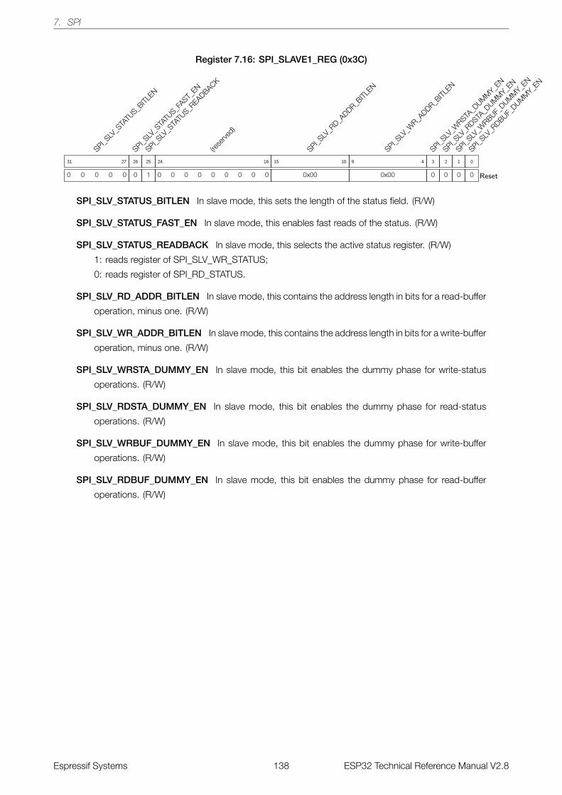
7. SPI
Register 7.16: SPI_SLAVE1_REG (0x3C)
SPI_SLV
_STA
TUS_B
ITLEN
0 0 0 0 0
31 27
SPI_SLV
_STA
TUS_F
AST_EN
0
26
SPI_SLV
_STA
TUS_R
EADBACK
1
25
(rese
rved)
0 0 0 0 0 0 0 0 0
24 16
SPI_SLV
_RD_A
DDR_BITL
EN
0x00
15 10
SPI_SLV
_WR_A
DDR_BITL
EN
0x00
9 4
SPI_SLV
_WRSTA
_DUM
MY_E
N
0
3
SPI_SLV
_RDSTA
_DUM
MY_E
N
0
2
SPI_SLV
_WRBUF_
DUMM
Y_EN
0
1
SPI_SLV
_RDBUF_
DUMM
Y_EN
0
0
Reset
SPI_SLV_STATUS_BITLEN In slave mode, this sets the length of the status field. (R/W)
SPI_SLV_STATUS_FAST_EN In slave mode, this enables fast reads of the status. (R/W)
SPI_SLV_STATUS_READBACK In slave mode, this selects the active status register. (R/W)
1: reads register of SPI_SLV_WR_STATUS;
0: reads register of SPI_RD_STATUS.
SPI_SLV_RD_ADDR_BITLEN In slave mode, this contains the address length in bits for a read-buffer
operation, minus one. (R/W)
SPI_SLV_WR_ADDR_BITLEN In slave mode, this contains the address length in bits for a write-buffer
operation, minus one. (R/W)
SPI_SLV_WRSTA_DUMMY_EN In slave mode, this bit enables the dummy phase for write-status
operations. (R/W)
SPI_SLV_RDSTA_DUMMY_EN In slave mode, this bit enables the dummy phase for read-status
operations. (R/W)
SPI_SLV_WRBUF_DUMMY_EN In slave mode, this bit enables the dummy phase for write-buffer
operations. (R/W)
SPI_SLV_RDBUF_DUMMY_EN In slave mode, this bit enables the dummy phase for read-buffer
operations. (R/W)
Espressif Systems 138 ESP32 Technical Reference Manual V2.8
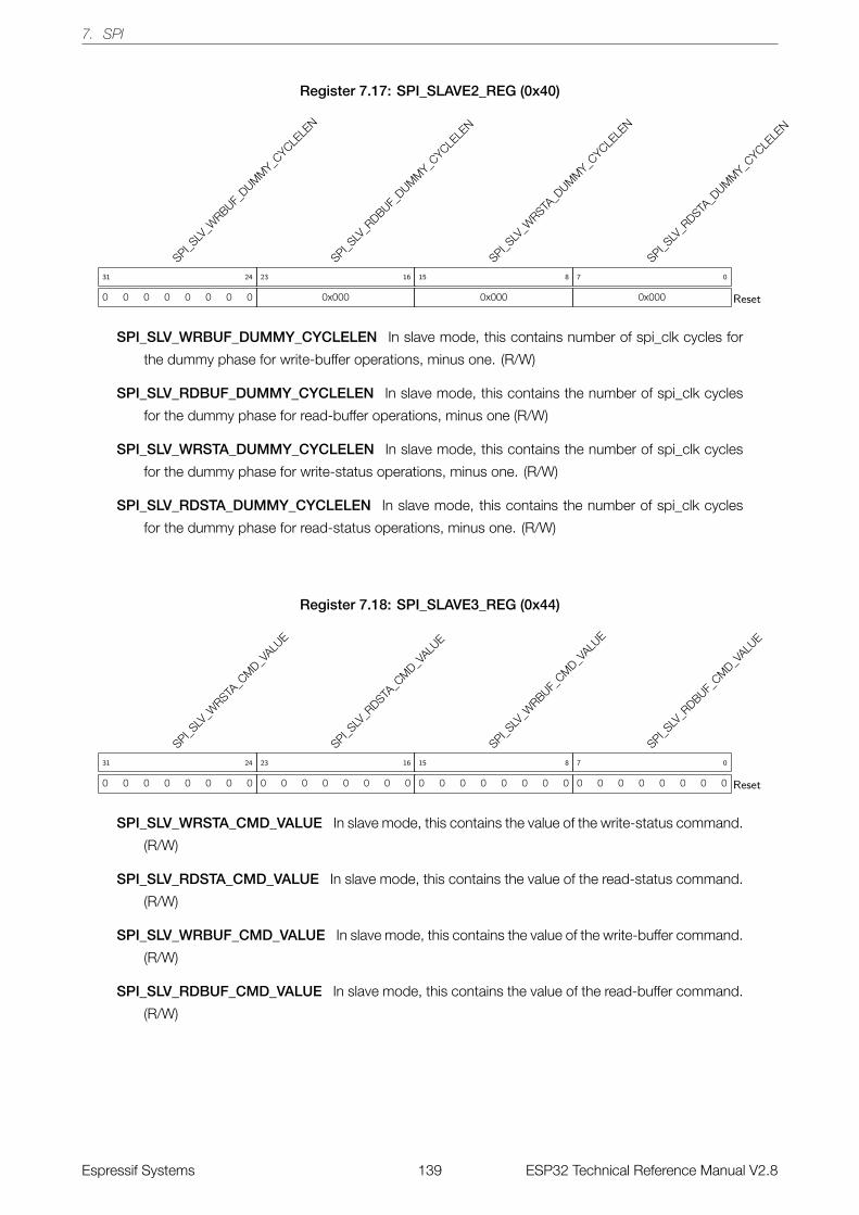
7. SPI
Register 7.17: SPI_SLAVE2_REG (0x40)
SPI_SLV
_WRBUF_
DUMM
Y_CYCLE
LEN
0 0 0 0 0 0 0 0
31 24
SPI_SLV
_RDBUF_
DUMM
Y_CYCLE
LEN
0x000
23 16
SPI_SLV
_WRSTA
_DUM
MY_C
YCLELE
N
0x000
15 8
SPI_SLV
_RDSTA
_DUM
MY_C
YCLELE
N
0x000
7 0
Reset
SPI_SLV_WRBUF_DUMMY_CYCLELEN In slave mode, this contains number of spi_clk cycles for
the dummy phase for write-buffer operations, minus one. (R/W)
SPI_SLV_RDBUF_DUMMY_CYCLELEN In slave mode, this contains the number of spi_clk cycles
for the dummy phase for read-buffer operations, minus one (R/W)
SPI_SLV_WRSTA_DUMMY_CYCLELEN In slave mode, this contains the number of spi_clk cycles
for the dummy phase for write-status operations, minus one. (R/W)
SPI_SLV_RDSTA_DUMMY_CYCLELEN In slave mode, this contains the number of spi_clk cycles
for the dummy phase for read-status operations, minus one. (R/W)
Register 7.18: SPI_SLAVE3_REG (0x44)
SPI_SLV
_WRSTA
_CM
D_VALU
E
0 0 0 0 0 0 0 0
31 24
SPI_SLV
_RDSTA
_CM
D_VALU
E
0 0 0 0 0 0 0 0
23 16
SPI_SLV
_WRBUF_
CMD_V
ALUE
0 0 0 0 0 0 0 0
15 8
SPI_SLV
_RDBUF_
CMD_V
ALUE
0 0 0 0 0 0 0 0
7 0
Reset
SPI_SLV_WRSTA_CMD_VALUE In slave mode, this contains the value of the write-status command.
(R/W)
SPI_SLV_RDSTA_CMD_VALUE In slave mode, this contains the value of the read-status command.
(R/W)
SPI_SLV_WRBUF_CMD_VALUE In slave mode, this contains the value of the write-buffer command.
(R/W)
SPI_SLV_RDBUF_CMD_VALUE In slave mode, this contains the value of the read-buffer command.
(R/W)
Espressif Systems 139 ESP32 Technical Reference Manual V2.8
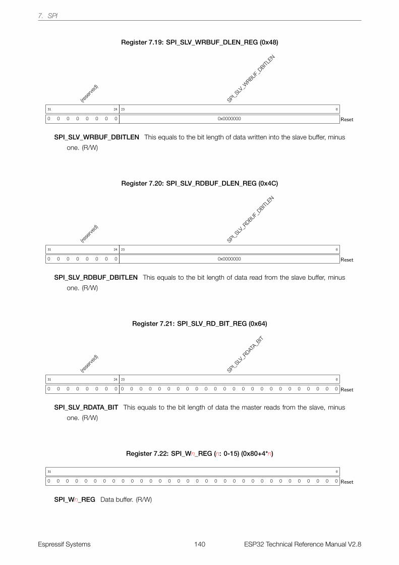
7. SPI
Register 7.19: SPI_SLV_WRBUF_DLEN_REG (0x48)
(rese
rved)
0 0 0 0 0 0 0 0
31 24
SPI_SLV
_WRBUF_
DBITLEN
0x0000000
23 0
Reset
SPI_SLV_WRBUF_DBITLEN This equals to the bit length of data written into the slave buffer, minus
one. (R/W)
Register 7.20: SPI_SLV_RDBUF_DLEN_REG (0x4C)
(rese
rved)
0 0 0 0 0 0 0 0
31 24
SPI_SLV
_RDBUF_
DBITLEN
0x0000000
23 0
Reset
SPI_SLV_RDBUF_DBITLEN This equals to the bit length of data read from the slave buffer, minus
one. (R/W)
Register 7.21: SPI_SLV_RD_BIT_REG (0x64)
(rese
rved)
0 0 0 0 0 0 0 0
31 24
SPI_SLV
_RDAT
A_BIT
0 0 0 0 0 0 0 0 0 0 0 0 0 0 0 0 0 0 0 0 0 0 0 0
23 0
Reset
SPI_SLV_RDATA_BIT This equals to the bit length of data the master reads from the slave, minus
one. (R/W)
Register 7.22: SPI_Wn_REG (n: 0-15) (0x80+4*n)
0 0 0 0 0 0 0 0 0 0 0 0 0 0 0 0 0 0 0 0 0 0 0 0 0 0 0 0 0 0 0 0
31 0
Reset
SPI_Wn_REG Data buffer. (R/W)
Espressif Systems 140 ESP32 Technical Reference Manual V2.8
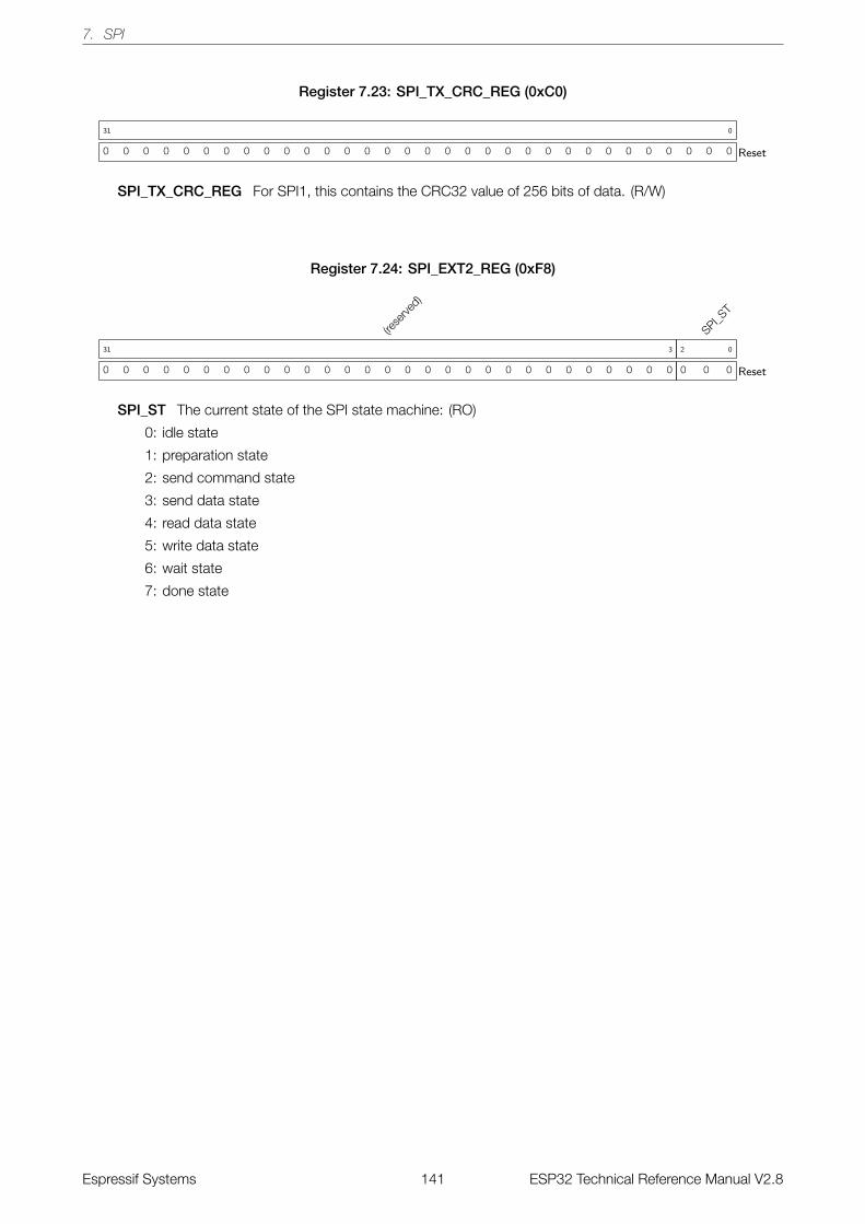
7. SPI
Register 7.23: SPI_TX_CRC_REG (0xC0)
0 0 0 0 0 0 0 0 0 0 0 0 0 0 0 0 0 0 0 0 0 0 0 0 0 0 0 0 0 0 0 0
31 0
Reset
SPI_TX_CRC_REG For SPI1, this contains the CRC32 value of 256 bits of data. (R/W)
Register 7.24: SPI_EXT2_REG (0xF8)
(rese
rved)
0 0 0 0 0 0 0 0 0 0 0 0 0 0 0 0 0 0 0 0 0 0 0 0 0 0 0 0 0
31 3
SPI_ST
0 0 0
2 0
Reset
SPI_ST The current state of the SPI state machine: (RO)
0: idle state
1: preparation state
2: send command state
3: send data state
4: read data state
5: write data state
6: wait state
7: done state
Espressif Systems 141 ESP32 Technical Reference Manual V2.8
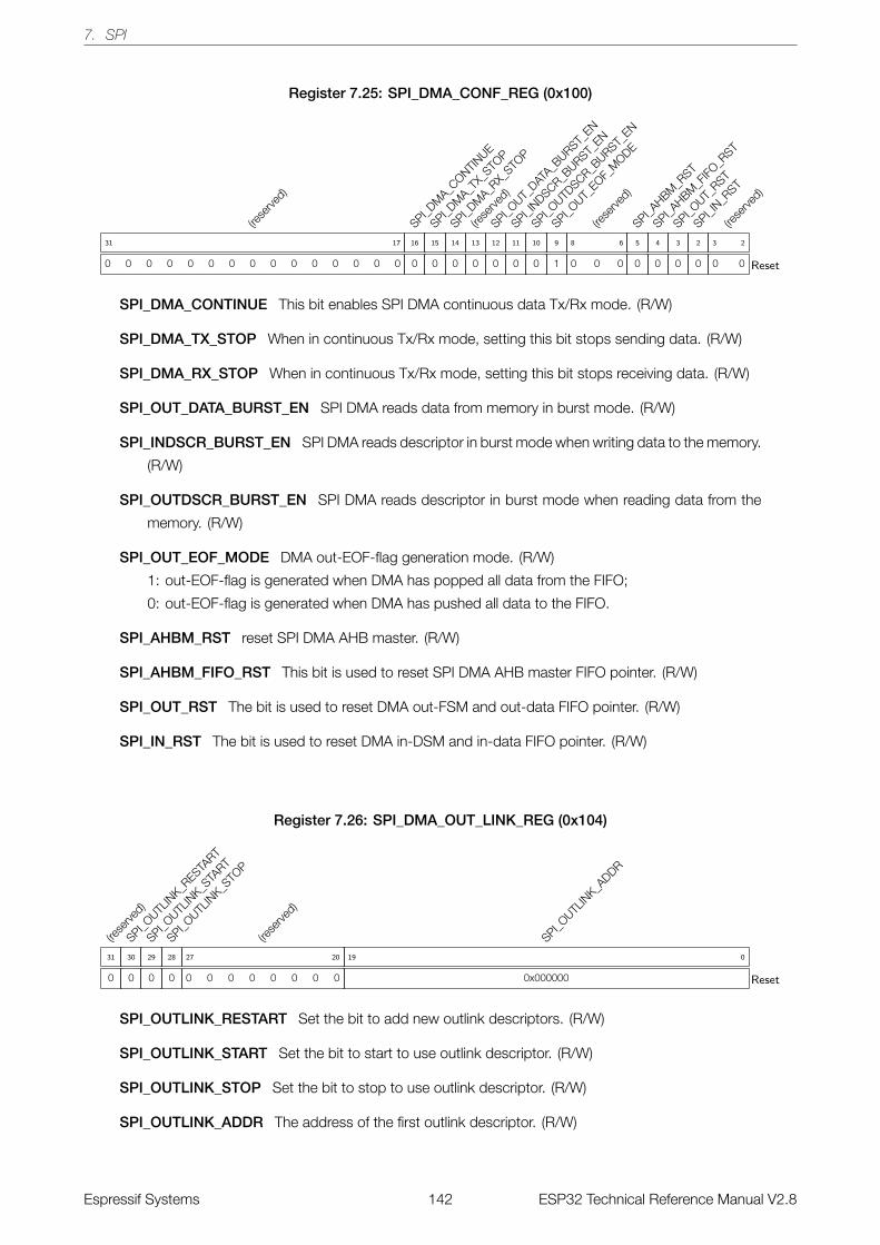
7. SPI
Register 7.25: SPI_DMA_CONF_REG (0x100)
(rese
rved)
0 0 0 0 0 0 0 0 0 0 0 0 0 0 0
31 17
SPI_DM
A_CONTIN
UE
0
16
SPI_DM
A_TX_
STOP
0
15
SPI_DM
A_RX_
STOP
0
14
(rese
rved)
0
13
SPI_OUT_
DATA_B
URST_EN
0
12
SPI_INDSCR_B
URST_EN
0
11
SPI_OUTD
SCR_BURST_
EN
0
10
SPI_OUT_
EOF_M
ODE
1
9
(rese
rved)
0 0 0
8 6
SPI_AHBM
_RST
0
5
SPI_AHBM
_FIFO
_RST
0
4
SPI_OUT_
RST
0
3
SPI_IN_R
ST
0
2
(rese
rved)
0 0
3 2
Reset
SPI_DMA_CONTINUE This bit enables SPI DMA continuous data Tx/Rx mode. (R/W)
SPI_DMA_TX_STOP When in continuous Tx/Rx mode, setting this bit stops sending data. (R/W)
SPI_DMA_RX_STOP When in continuous Tx/Rx mode, setting this bit stops receiving data. (R/W)
SPI_OUT_DATA_BURST_EN SPI DMA reads data from memory in burst mode. (R/W)
SPI_INDSCR_BURST_EN SPI DMA reads descriptor in burst mode when writing data to the memory.
(R/W)
SPI_OUTDSCR_BURST_EN SPI DMA reads descriptor in burst mode when reading data from the
memory. (R/W)
SPI_OUT_EOF_MODE DMA out-EOF-flag generation mode. (R/W)
1: out-EOF-flag is generated when DMA has popped all data from the FIFO;
0: out-EOF-flag is generated when DMA has pushed all data to the FIFO.
SPI_AHBM_RST reset SPI DMA AHB master. (R/W)
SPI_AHBM_FIFO_RST This bit is used to reset SPI DMA AHB master FIFO pointer. (R/W)
SPI_OUT_RST The bit is used to reset DMA out-FSM and out-data FIFO pointer. (R/W)
SPI_IN_RST The bit is used to reset DMA in-DSM and in-data FIFO pointer. (R/W)
Register 7.26: SPI_DMA_OUT_LINK_REG (0x104)
(rese
rved)
0
31
SPI_OUTL
INK_R
ESTART
0
30
SPI_OUTL
INK_S
TART
0
29
SPI_OUTL
INK_S
TOP
0
28
(rese
rved)
0 0 0 0 0 0 0 0
27 20
SPI_OUTL
INK_A
DDR
0x000000
19 0
Reset
SPI_OUTLINK_RESTART Set the bit to add new outlink descriptors. (R/W)
SPI_OUTLINK_START Set the bit to start to use outlink descriptor. (R/W)
SPI_OUTLINK_STOP Set the bit to stop to use outlink descriptor. (R/W)
SPI_OUTLINK_ADDR The address of the first outlink descriptor. (R/W)
Espressif Systems 142 ESP32 Technical Reference Manual V2.8
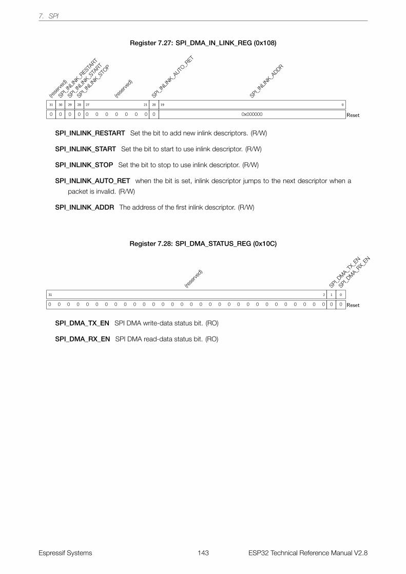
7. SPI
Register 7.27: SPI_DMA_IN_LINK_REG (0x108)
(rese
rved)
0
31
SPI_INLIN
K_RESTA
RT
0
30
SPI_INLIN
K_STA
RT
0
29
SPI_INLIN
K_STO
P
0
28
(rese
rved)
0 0 0 0 0 0 0
27 21
SPI_INLIN
K_AUTO
_RET
0
20
SPI_INLIN
K_ADDR
0x000000
19 0
Reset
SPI_INLINK_RESTART Set the bit to add new inlink descriptors. (R/W)
SPI_INLINK_START Set the bit to start to use inlink descriptor. (R/W)
SPI_INLINK_STOP Set the bit to stop to use inlink descriptor. (R/W)
SPI_INLINK_AUTO_RET when the bit is set, inlink descriptor jumps to the next descriptor when a
packet is invalid. (R/W)
SPI_INLINK_ADDR The address of the first inlink descriptor. (R/W)
Register 7.28: SPI_DMA_STATUS_REG (0x10C)
(rese
rved)
0 0 0 0 0 0 0 0 0 0 0 0 0 0 0 0 0 0 0 0 0 0 0 0 0 0 0 0 0 0
31 2
SPI_DM
A_TX_
EN
0
1
SPI_DM
A_RX_
EN
0
0
Reset
SPI_DMA_TX_EN SPI DMA write-data status bit. (RO)
SPI_DMA_RX_EN SPI DMA read-data status bit. (RO)
Espressif Systems 143 ESP32 Technical Reference Manual V2.8
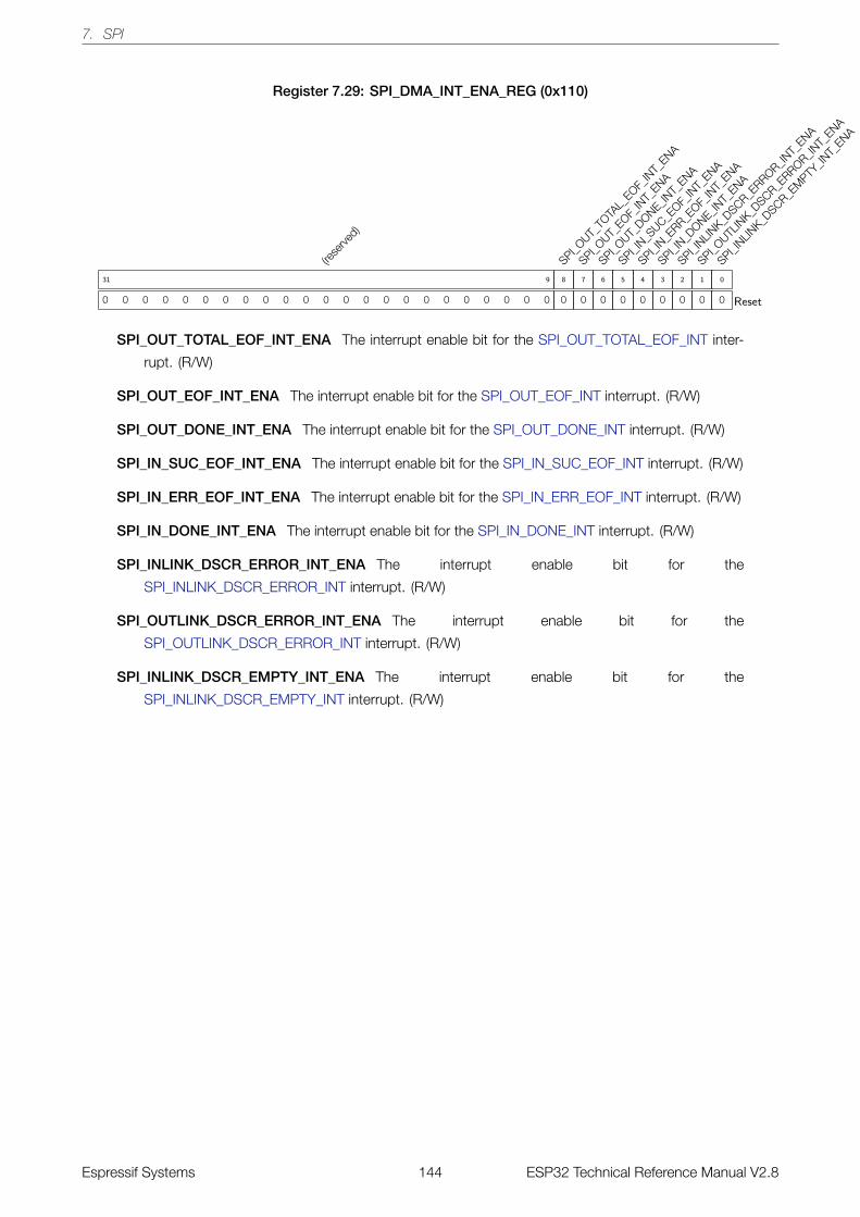
7. SPI
Register 7.29: SPI_DMA_INT_ENA_REG (0x110)
(rese
rved)
0 0 0 0 0 0 0 0 0 0 0 0 0 0 0 0 0 0 0 0 0 0 0
31 9
SPI_OUT_
TOTA
L_EOF_
INT_
ENA
0
8
SPI_OUT_
EOF_IN
T_ENA
0
7
SPI_OUT_
DONE_INT_
ENA
0
6
SPI_IN_S
UC_EOF_
INT_
ENA
0
5
SPI_IN_E
RR_EOF_
INT_
ENA
0
4
SPI_IN_D
ONE_INT_
ENA
0
3
SPI_INLIN
K_DSCR_E
RROR_INT_
ENA
0
2
SPI_OUTL
INK_D
SCR_ERROR_IN
T_ENA
0
1
SPI_INLIN
K_DSCR_E
MPTY
_INT_
ENA
0
0
Reset
SPI_OUT_TOTAL_EOF_INT_ENA The interrupt enable bit for the SPI_OUT_TOTAL_EOF_INT inter-
rupt. (R/W)
SPI_OUT_EOF_INT_ENA The interrupt enable bit for the SPI_OUT_EOF_INT interrupt. (R/W)
SPI_OUT_DONE_INT_ENA The interrupt enable bit for the SPI_OUT_DONE_INT interrupt. (R/W)
SPI_IN_SUC_EOF_INT_ENA The interrupt enable bit for the SPI_IN_SUC_EOF_INT interrupt. (R/W)
SPI_IN_ERR_EOF_INT_ENA The interrupt enable bit for the SPI_IN_ERR_EOF_INT interrupt. (R/W)
SPI_IN_DONE_INT_ENA The interrupt enable bit for the SPI_IN_DONE_INT interrupt. (R/W)
SPI_INLINK_DSCR_ERROR_INT_ENA The interrupt enable bit for the
SPI_INLINK_DSCR_ERROR_INT interrupt. (R/W)
SPI_OUTLINK_DSCR_ERROR_INT_ENA The interrupt enable bit for the
SPI_OUTLINK_DSCR_ERROR_INT interrupt. (R/W)
SPI_INLINK_DSCR_EMPTY_INT_ENA The interrupt enable bit for the
SPI_INLINK_DSCR_EMPTY_INT interrupt. (R/W)
Espressif Systems 144 ESP32 Technical Reference Manual V2.8
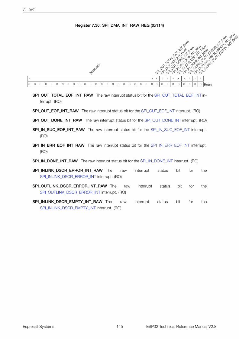
7. SPI
Register 7.30: SPI_DMA_INT_RAW_REG (0x114)
(rese
rved)
0 0 0 0 0 0 0 0 0 0 0 0 0 0 0 0 0 0 0 0 0 0 0
31 9
SPI_OUT_
TOTA
L_EOF_
INT_
RAW
0
8
SPI_OUT_
EOF_IN
T_RAW
0
7
SPI_OUT_
DONE_INT_
RAW
0
6
SPI_IN_S
UC_EOF_
INT_
RAW
0
5
SPI_IN_E
RR_EOF_
INT_
RAW
0
4
SPI_IN_D
ONE_INT_
RAW
0
3
SPI_INLIN
K_DSCR_E
RROR_INT_
RAW
0
2
SPI_OUTL
INK_D
SCR_ERROR_IN
T_RAW
0
1
SPI_INLIN
K_DSCR_E
MPTY
_INT_
RAW
0
0
Reset
SPI_OUT_TOTAL_EOF_INT_RAW The raw interrupt status bit for the SPI_OUT_TOTAL_EOF_INT in-
terrupt. (RO)
SPI_OUT_EOF_INT_RAW The raw interrupt status bit for the SPI_OUT_EOF_INT interrupt. (RO)
SPI_OUT_DONE_INT_RAW The raw interrupt status bit for the SPI_OUT_DONE_INT interrupt. (RO)
SPI_IN_SUC_EOF_INT_RAW The raw interrupt status bit for the SPI_IN_SUC_EOF_INT interrupt.
(RO)
SPI_IN_ERR_EOF_INT_RAW The raw interrupt status bit for the SPI_IN_ERR_EOF_INT interrupt.
(RO)
SPI_IN_DONE_INT_RAW The raw interrupt status bit for the SPI_IN_DONE_INT interrupt. (RO)
SPI_INLINK_DSCR_ERROR_INT_RAW The raw interrupt status bit for the
SPI_INLINK_DSCR_ERROR_INT interrupt. (RO)
SPI_OUTLINK_DSCR_ERROR_INT_RAW The raw interrupt status bit for the
SPI_OUTLINK_DSCR_ERROR_INT interrupt. (RO)
SPI_INLINK_DSCR_EMPTY_INT_RAW The raw interrupt status bit for the
SPI_INLINK_DSCR_EMPTY_INT interrupt. (RO)
Espressif Systems 145 ESP32 Technical Reference Manual V2.8
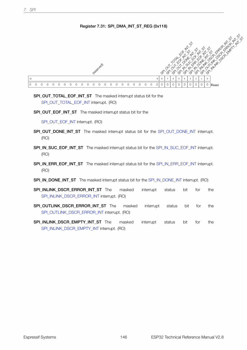
7. SPI
Register 7.31: SPI_DMA_INT_ST_REG (0x118)
(rese
rved)
0 0 0 0 0 0 0 0 0 0 0 0 0 0 0 0 0 0 0 0 0 0 0
31 9
SPI_OUT_
TOTA
L_EOF_
INT_
ST
0
8
SPI_OUT_
EOF_IN
T_ST
0
7
SPI_OUT_
DONE_INT_
ST
0
6
SPI_IN_S
UC_EOF_
INT_
ST
0
5
SPI_IN_E
RR_EOF_
INT_
ST
0
4
SPI_IN_D
ONE_INT_
ST
0
3
SPI_INLIN
K_DSCR_E
RROR_INT_
ST
0
2
SPI_OUTL
INK_D
SCR_ERROR_IN
T_ST
0
1
SPI_INLIN
K_DSCR_E
MPTY
_INT_
ST
0
0
Reset
SPI_OUT_TOTAL_EOF_INT_ST The masked interrupt status bit for the
SPI_OUT_TOTAL_EOF_INT interrupt. (RO)
SPI_OUT_EOF_INT_ST The masked interrupt status bit for the
SPI_OUT_EOF_INT interrupt. (RO)
SPI_OUT_DONE_INT_ST The masked interrupt status bit for the SPI_OUT_DONE_INT interrupt.
(RO)
SPI_IN_SUC_EOF_INT_ST The masked interrupt status bit for the SPI_IN_SUC_EOF_INT interrupt.
(RO)
SPI_IN_ERR_EOF_INT_ST The masked interrupt status bit for the SPI_IN_ERR_EOF_INT interrupt.
(RO)
SPI_IN_DONE_INT_ST The masked interrupt status bit for the SPI_IN_DONE_INT interrupt. (RO)
SPI_INLINK_DSCR_ERROR_INT_ST The masked interrupt status bit for the
SPI_INLINK_DSCR_ERROR_INT interrupt. (RO)
SPI_OUTLINK_DSCR_ERROR_INT_ST The masked interrupt status bit for the
SPI_OUTLINK_DSCR_ERROR_INT interrupt. (RO)
SPI_INLINK_DSCR_EMPTY_INT_ST The masked interrupt status bit for the
SPI_INLINK_DSCR_EMPTY_INT interrupt. (RO)
Espressif Systems 146 ESP32 Technical Reference Manual V2.8
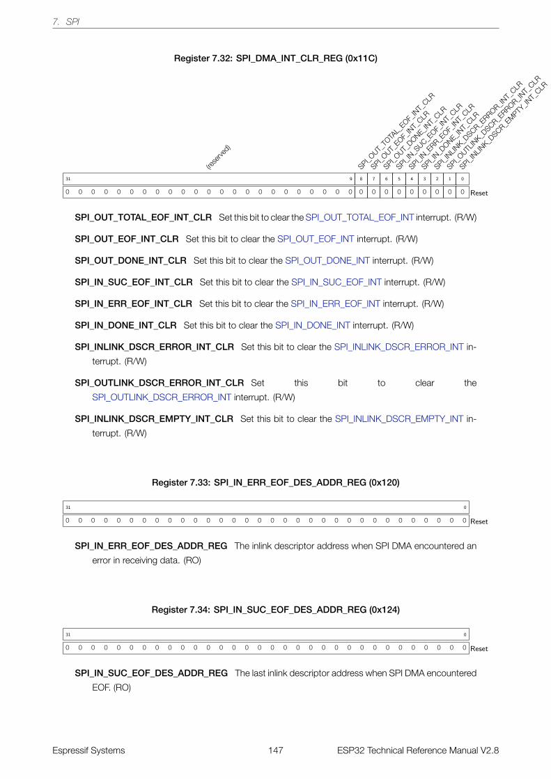
7. SPI
Register 7.32: SPI_DMA_INT_CLR_REG (0x11C)
(rese
rved)
0 0 0 0 0 0 0 0 0 0 0 0 0 0 0 0 0 0 0 0 0 0 0
31 9
SPI_OUT_
TOTA
L_EOF_
INT_
CLR
0
8
SPI_OUT_
EOF_IN
T_CLR
0
7
SPI_OUT_
DONE_INT_
CLR
0
6
SPI_IN_S
UC_EOF_
INT_
CLR
0
5
SPI_IN_E
RR_EOF_
INT_
CLR
0
4
SPI_IN_D
ONE_INT_
CLR
0
3
SPI_INLIN
K_DSCR_E
RROR_INT_
CLR
0
2
SPI_OUTL
INK_D
SCR_ERROR_IN
T_CLR
0
1
SPI_INLIN
K_DSCR_E
MPTY
_INT_
CLR
0
0
Reset
SPI_OUT_TOTAL_EOF_INT_CLR Set this bit to clear the SPI_OUT_TOTAL_EOF_INT interrupt. (R/W)
SPI_OUT_EOF_INT_CLR Set this bit to clear the SPI_OUT_EOF_INT interrupt. (R/W)
SPI_OUT_DONE_INT_CLR Set this bit to clear the SPI_OUT_DONE_INT interrupt. (R/W)
SPI_IN_SUC_EOF_INT_CLR Set this bit to clear the SPI_IN_SUC_EOF_INT interrupt. (R/W)
SPI_IN_ERR_EOF_INT_CLR Set this bit to clear the SPI_IN_ERR_EOF_INT interrupt. (R/W)
SPI_IN_DONE_INT_CLR Set this bit to clear the SPI_IN_DONE_INT interrupt. (R/W)
SPI_INLINK_DSCR_ERROR_INT_CLR Set this bit to clear the SPI_INLINK_DSCR_ERROR_INT in-
terrupt. (R/W)
SPI_OUTLINK_DSCR_ERROR_INT_CLR Set this bit to clear the
SPI_OUTLINK_DSCR_ERROR_INT interrupt. (R/W)
SPI_INLINK_DSCR_EMPTY_INT_CLR Set this bit to clear the SPI_INLINK_DSCR_EMPTY_INT in-
terrupt. (R/W)
Register 7.33: SPI_IN_ERR_EOF_DES_ADDR_REG (0x120)
0 0 0 0 0 0 0 0 0 0 0 0 0 0 0 0 0 0 0 0 0 0 0 0 0 0 0 0 0 0 0 0
31 0
Reset
SPI_IN_ERR_EOF_DES_ADDR_REG The inlink descriptor address when SPI DMA encountered an
error in receiving data. (RO)
Register 7.34: SPI_IN_SUC_EOF_DES_ADDR_REG (0x124)
0 0 0 0 0 0 0 0 0 0 0 0 0 0 0 0 0 0 0 0 0 0 0 0 0 0 0 0 0 0 0 0
31 0
Reset
SPI_IN_SUC_EOF_DES_ADDR_REG The last inlink descriptor address when SPI DMA encountered
EOF. (RO)
Espressif Systems 147 ESP32 Technical Reference Manual V2.8
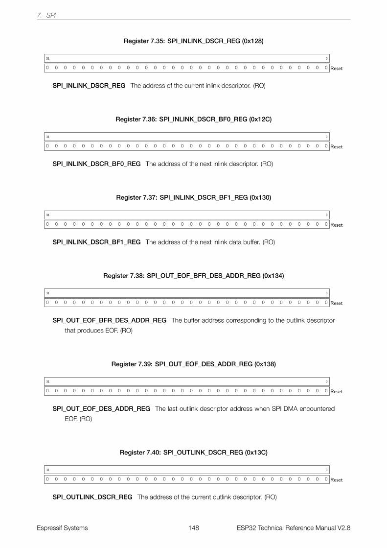
7. SPI
Register 7.35: SPI_INLINK_DSCR_REG (0x128)
0 0 0 0 0 0 0 0 0 0 0 0 0 0 0 0 0 0 0 0 0 0 0 0 0 0 0 0 0 0 0 0
31 0
Reset
SPI_INLINK_DSCR_REG The address of the current inlink descriptor. (RO)
Register 7.36: SPI_INLINK_DSCR_BF0_REG (0x12C)
0 0 0 0 0 0 0 0 0 0 0 0 0 0 0 0 0 0 0 0 0 0 0 0 0 0 0 0 0 0 0 0
31 0
Reset
SPI_INLINK_DSCR_BF0_REG The address of the next inlink descriptor. (RO)
Register 7.37: SPI_INLINK_DSCR_BF1_REG (0x130)
0 0 0 0 0 0 0 0 0 0 0 0 0 0 0 0 0 0 0 0 0 0 0 0 0 0 0 0 0 0 0 0
31 0
Reset
SPI_INLINK_DSCR_BF1_REG The address of the next inlink data buffer. (RO)
Register 7.38: SPI_OUT_EOF_BFR_DES_ADDR_REG (0x134)
0 0 0 0 0 0 0 0 0 0 0 0 0 0 0 0 0 0 0 0 0 0 0 0 0 0 0 0 0 0 0 0
31 0
Reset
SPI_OUT_EOF_BFR_DES_ADDR_REG The buffer address corresponding to the outlink descriptor
that produces EOF. (RO)
Register 7.39: SPI_OUT_EOF_DES_ADDR_REG (0x138)
0 0 0 0 0 0 0 0 0 0 0 0 0 0 0 0 0 0 0 0 0 0 0 0 0 0 0 0 0 0 0 0
31 0
Reset
SPI_OUT_EOF_DES_ADDR_REG The last outlink descriptor address when SPI DMA encountered
EOF. (RO)
Register 7.40: SPI_OUTLINK_DSCR_REG (0x13C)
0 0 0 0 0 0 0 0 0 0 0 0 0 0 0 0 0 0 0 0 0 0 0 0 0 0 0 0 0 0 0 0
31 0
Reset
SPI_OUTLINK_DSCR_REG The address of the current outlink descriptor. (RO)
Espressif Systems 148 ESP32 Technical Reference Manual V2.8
7. SPI
Register 7.41: SPI_OUTLINK_DSCR_BF0_REG (0x140)
0 0 0 0 0 0 0 0 0 0 0 0 0 0 0 0 0 0 0 0 0 0 0 0 0 0 0 0 0 0 0 0
31 0
Reset
SPI_OUTLINK_DSCR_BF0_REG The address of the next outlink descriptor. (RO)
Register 7.42: SPI_OUTLINK_DSCR_BF1_REG (0x144)
0 0 0 0 0 0 0 0 0 0 0 0 0 0 0 0 0 0 0 0 0 0 0 0 0 0 0 0 0 0 0 0
31 0
Reset
SPI_OUTLINK_DSCR_BF1_REG The address of the next outlink data buffer. (RO)
Register 7.43: SPI_DMA_RSTATUS_REG (0x148)
TX_F
IFO_E
MPTY
0
31
TX_F
IFO_F
ULL
0
30
(rese
rved)
0 0 0 0 0 0 0 0 0 0
29 20
TX_D
ES_ADDRESS
0 0 0 0 0 0 0 0 0 0 0 0 0 0 0 0 0 0 0 0
19 0
Reset
TX_FIFO_EMPTY The SPI DMA Tx FIFO is empty. (RO)
TX_FIFO_FULL The SPI DMA Tx FIFO is full. (RO)
TX_DES_ADDRESS The LSB of the SPI DMA outlink descriptor address. (RO)
Register 7.44: SPI_DMA_TSTATUS_REG (0x14C)
RX_FIF
O_EM
PTY
0
31
RX_FIF
O_FULL
0
30
(rese
rved)
0 0 0 0 0 0 0 0 0 0
29 20
RX_DES_A
DDRESS
0 0 0 0 0 0 0 0 0 0 0 0 0 0 0 0 0 0 0 0
19 0
Reset
RX_FIFO_EMPTY The SPI DMA Rx FIFO is empty. (RO)
RX_FIFO_FULL The SPI DMA Rx FIFO is full. (RO)
RX_DES_ADDRESS The LSB of the SPI DMA inlink descriptor address. (RO)
Espressif Systems 149 ESP32 Technical Reference Manual V2.8
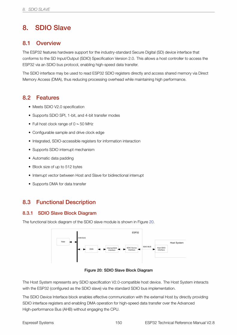
8. SDIO SLAVE
8. SDIO Slave
8.1 Overview
The ESP32 features hardware support for the industry-standard Secure Digital (SD) device interface that
conforms to the SD Input/Output (SDIO) Specification Version 2.0. This allows a host controller to access the
ESP32 via an SDIO bus protocol, enabling high-speed data transfer.
The SDIO interface may be used to read ESP32 SDIO registers directly and access shared memory via Direct
Memory Access (DMA), thus reducing processing overhead while maintaining high performance.
8.2 Features
• Meets SDIO V2.0 specification
• Supports SDIO SPI, 1-bit, and 4-bit transfer modes
• Full host clock range of 0 ~ 50 MHz
• Configurable sample and drive clock edge
• Integrated, SDIO-accessible registers for information interaction
• Supports SDIO interrupt mechanism
• Automatic data padding
• Block size of up to 512 bytes
• Interrupt vector between Host and Slave for bidirectional interrupt
• Supports DMA for data transfer
8.3 Functional Description
8.3.1 SDIO Slave Block Diagram
The functional block diagram of the SDIO slave module is shown in Figure 20.
Figure 20: SDIO Slave Block Diagram
The Host System represents any SDIO specification V2.0-compatible host device. The Host System interacts
with the ESP32 (configured as the SDIO slave) via the standard SDIO bus implementation.
The SDIO Device Interface block enables effective communication with the external Host by directly providing
SDIO interface registers and enabling DMA operation for high-speed data transfer over the Advanced
High-performance Bus (AHB) without engaging the CPU.
Espressif Systems 150 ESP32 Technical Reference Manual V2.8
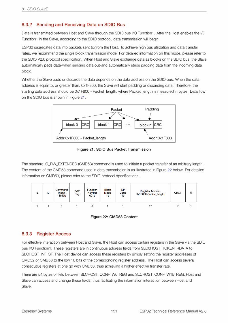
8. SDIO SLAVE
8.3.2 Sending and Receiving Data on SDIO Bus
Data is transmitted between Host and Slave through the SDIO bus I/O Function1. After the Host enables the I/O
Function1 in the Slave, according to the SDIO protocol, data transmission will begin.
ESP32 segregates data into packets sent to/from the Host. To achieve high bus utilization and data transfer
rates, we recommend the single block transmission mode. For detailed information on this mode, please refer to
the SDIO V2.0 protocol specification. When Host and Slave exchange data as blocks on the SDIO bus, the Slave
automatically pads data-when sending data out-and automatically strips padding data from the incoming data
block.
Whether the Slave pads or discards the data depends on the data address on the SDIO bus. When the data
address is equal to, or greater than, 0x1F800, the Slave will start padding or discarding data. Therefore, the
starting data address should be 0x1F800 - Packet_length, where Packet_length is measured in bytes. Data flow
on the SDIO bus is shown in Figure 21.
Figure 21: SDIO Bus Packet Transmission
The standard IO_RW_EXTENDED (CMD53) command is used to initiate a packet transfer of an arbitrary length.
The content of the CMD53 command used in data transmission is as illustrated in Figure 22 below. For detailed
information on CMD53, please refer to the SDIO protocol specifications.
DCommand
Index11010b
S
1
R/WFlag
FunctionNumber
001b
BlockMode
1b
OPCode
1b
Register Address0x1F800-Packet_length
CRC7 E
1 6 1 3 1 1 17 7 1
Figure 22: CMD53 Content
8.3.3 Register Access
For effective interaction between Host and Slave, the Host can access certain registers in the Slave via the SDIO
bus I/O Function1. These registers are in continuous address fields from SLC0HOST_TOKEN_RDATA to
SLCHOST_INF_ST. The Host device can access these registers by simply setting the register addresses of
CMD52 or CMD53 to the low 10 bits of the corresponding register address. The Host can access several
consecutive registers at one go with CMD53, thus achieving a higher effective transfer rate.
There are 54 bytes of field between SLCHOST_CONF_W0_REG and SLCHOST_CONF_W15_REG. Host and
Slave can access and change these fields, thus facilitating the information interaction between Host and
Slave.
Espressif Systems 151 ESP32 Technical Reference Manual V2.8
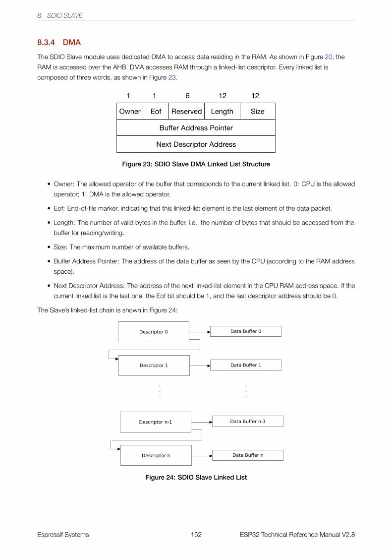
8. SDIO SLAVE
8.3.4 DMA
The SDIO Slave module uses dedicated DMA to access data residing in the RAM. As shown in Figure 20, the
RAM is accessed over the AHB. DMA accesses RAM through a linked-list descriptor. Every linked list is
composed of three words, as shown in Figure 23.
Figure 23: SDIO Slave DMA Linked List Structure
• Owner: The allowed operator of the buffer that corresponds to the current linked list. 0: CPU is the allowed
operator; 1: DMA is the allowed operator.
• Eof: End-of-file marker, indicating that this linked-list element is the last element of the data packet.
• Length: The number of valid bytes in the buffer, i.e., the number of bytes that should be accessed from the
buffer for reading/writing.
• Size: The maximum number of available buffers.
• Buffer Address Pointer: The address of the data buffer as seen by the CPU (according to the RAM address
space).
• Next Descriptor Address: The address of the next linked-list element in the CPU RAM address space. If the
current linked list is the last one, the Eof bit should be 1, and the last descriptor address should be 0.
The Slave’s linked-list chain is shown in Figure 24:
Figure 24: SDIO Slave Linked List
Espressif Systems 152 ESP32 Technical Reference Manual V2.8
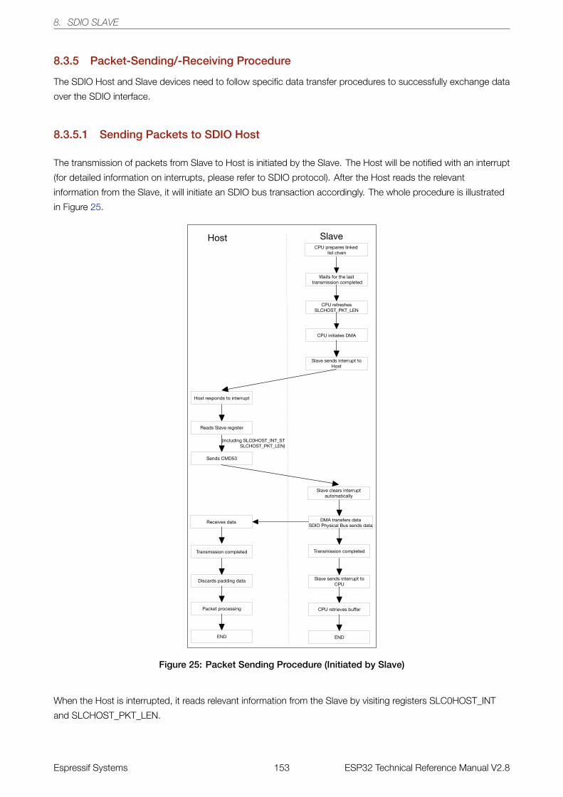
8. SDIO SLAVE
8.3.5 Packet-Sending/-Receiving Procedure
The SDIO Host and Slave devices need to follow specific data transfer procedures to successfully exchange data
over the SDIO interface.
8.3.5.1 Sending Packets to SDIO Host
The transmission of packets from Slave to Host is initiated by the Slave. The Host will be notified with an interrupt
(for detailed information on interrupts, please refer to SDIO protocol). After the Host reads the relevant
information from the Slave, it will initiate an SDIO bus transaction accordingly. The whole procedure is illustrated
in Figure 25.
Figure 25: Packet Sending Procedure (Initiated by Slave)
When the Host is interrupted, it reads relevant information from the Slave by visiting registers SLC0HOST_INT
and SLCHOST_PKT_LEN.
Espressif Systems 153 ESP32 Technical Reference Manual V2.8
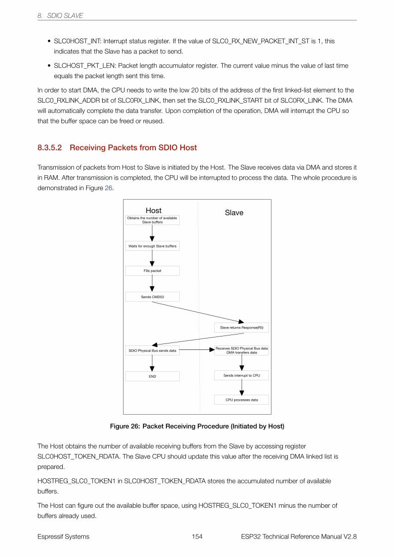
8. SDIO SLAVE
• SLC0HOST_INT: Interrupt status register. If the value of SLC0_RX_NEW_PACKET_INT_ST is 1, this
indicates that the Slave has a packet to send.
• SLCHOST_PKT_LEN: Packet length accumulator register. The current value minus the value of last time
equals the packet length sent this time.
In order to start DMA, the CPU needs to write the low 20 bits of the address of the first linked-list element to the
SLC0_RXLINK_ADDR bit of SLC0RX_LINK, then set the SLC0_RXLINK_START bit of SLC0RX_LINK. The DMA
will automatically complete the data transfer. Upon completion of the operation, DMA will interrupt the CPU so
that the buffer space can be freed or reused.
8.3.5.2 Receiving Packets from SDIO Host
Transmission of packets from Host to Slave is initiated by the Host. The Slave receives data via DMA and stores it
in RAM. After transmission is completed, the CPU will be interrupted to process the data. The whole procedure is
demonstrated in Figure 26.
Figure 26: Packet Receiving Procedure (Initiated by Host)
The Host obtains the number of available receiving buffers from the Slave by accessing register
SLC0HOST_TOKEN_RDATA. The Slave CPU should update this value after the receiving DMA linked list is
prepared.
HOSTREG_SLC0_TOKEN1 in SLC0HOST_TOKEN_RDATA stores the accumulated number of available
buffers.
The Host can figure out the available buffer space, using HOSTREG_SLC0_TOKEN1 minus the number of
buffers already used.
Espressif Systems 154 ESP32 Technical Reference Manual V2.8
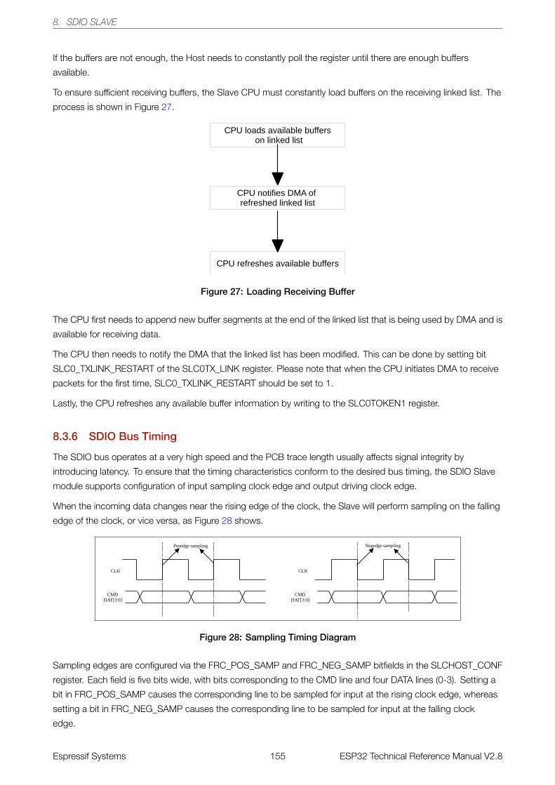
8. SDIO SLAVE
If the buffers are not enough, the Host needs to constantly poll the register until there are enough buffers
available.
To ensure sufficient receiving buffers, the Slave CPU must constantly load buffers on the receiving linked list. The
process is shown in Figure 27.
Figure 27: Loading Receiving Buffer
The CPU first needs to append new buffer segments at the end of the linked list that is being used by DMA and is
available for receiving data.
The CPU then needs to notify the DMA that the linked list has been modified. This can be done by setting bit
SLC0_TXLINK_RESTART of the SLC0TX_LINK register. Please note that when the CPU initiates DMA to receive
packets for the first time, SLC0_TXLINK_RESTART should be set to 1.
Lastly, the CPU refreshes any available buffer information by writing to the SLC0TOKEN1 register.
8.3.6 SDIO Bus Timing
The SDIO bus operates at a very high speed and the PCB trace length usually affects signal integrity by
introducing latency. To ensure that the timing characteristics conform to the desired bus timing, the SDIO Slave
module supports configuration of input sampling clock edge and output driving clock edge.
When the incoming data changes near the rising edge of the clock, the Slave will perform sampling on the falling
edge of the clock, or vice versa, as Figure 28 shows.
Figure 28: Sampling Timing Diagram
Sampling edges are configured via the FRC_POS_SAMP and FRC_NEG_SAMP bitfields in the SLCHOST_CONF
register. Each field is five bits wide, with bits corresponding to the CMD line and four DATA lines (0-3). Setting a
bit in FRC_POS_SAMP causes the corresponding line to be sampled for input at the rising clock edge, whereas
setting a bit in FRC_NEG_SAMP causes the corresponding line to be sampled for input at the falling clock
edge.
Espressif Systems 155 ESP32 Technical Reference Manual V2.8
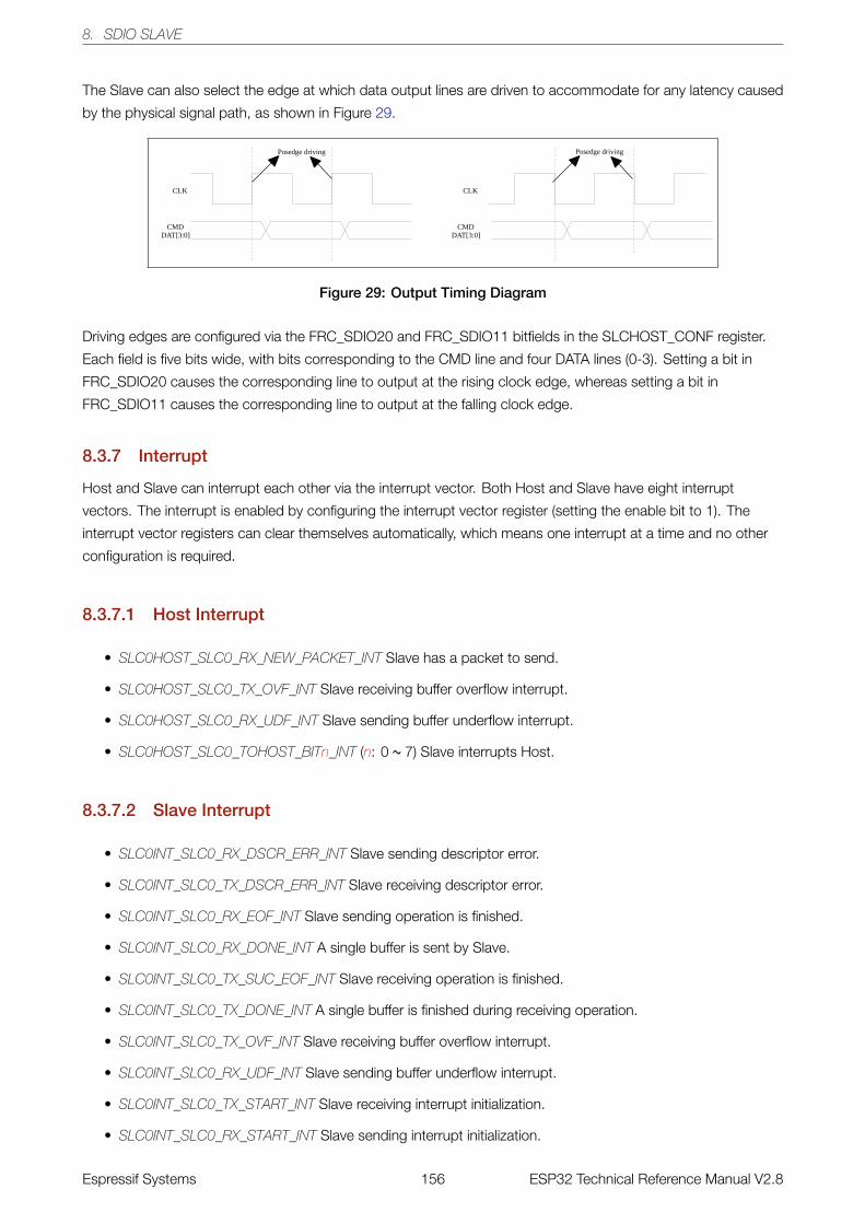
8. SDIO SLAVE
The Slave can also select the edge at which data output lines are driven to accommodate for any latency caused
by the physical signal path, as shown in Figure 29.
Figure 29: Output Timing Diagram
Driving edges are configured via the FRC_SDIO20 and FRC_SDIO11 bitfields in the SLCHOST_CONF register.
Each field is five bits wide, with bits corresponding to the CMD line and four DATA lines (0-3). Setting a bit in
FRC_SDIO20 causes the corresponding line to output at the rising clock edge, whereas setting a bit in
FRC_SDIO11 causes the corresponding line to output at the falling clock edge.
8.3.7 Interrupt
Host and Slave can interrupt each other via the interrupt vector. Both Host and Slave have eight interrupt
vectors. The interrupt is enabled by configuring the interrupt vector register (setting the enable bit to 1). The
interrupt vector registers can clear themselves automatically, which means one interrupt at a time and no other
configuration is required.
8.3.7.1 Host Interrupt
• SLC0HOST_SLC0_RX_NEW_PACKET_INT Slave has a packet to send.
• SLC0HOST_SLC0_TX_OVF_INT Slave receiving buffer overflow interrupt.
• SLC0HOST_SLC0_RX_UDF_INT Slave sending buffer underflow interrupt.
• SLC0HOST_SLC0_TOHOST_BITn_INT (n: 0 ~ 7) Slave interrupts Host.
8.3.7.2 Slave Interrupt
• SLC0INT_SLC0_RX_DSCR_ERR_INT Slave sending descriptor error.
• SLC0INT_SLC0_TX_DSCR_ERR_INT Slave receiving descriptor error.
• SLC0INT_SLC0_RX_EOF_INT Slave sending operation is finished.
• SLC0INT_SLC0_RX_DONE_INT A single buffer is sent by Slave.
• SLC0INT_SLC0_TX_SUC_EOF_INT Slave receiving operation is finished.
• SLC0INT_SLC0_TX_DONE_INT A single buffer is finished during receiving operation.
• SLC0INT_SLC0_TX_OVF_INT Slave receiving buffer overflow interrupt.
• SLC0INT_SLC0_RX_UDF_INT Slave sending buffer underflow interrupt.
• SLC0INT_SLC0_TX_START_INT Slave receiving interrupt initialization.
• SLC0INT_SLC0_RX_START_INT Slave sending interrupt initialization.
Espressif Systems 156 ESP32 Technical Reference Manual V2.8
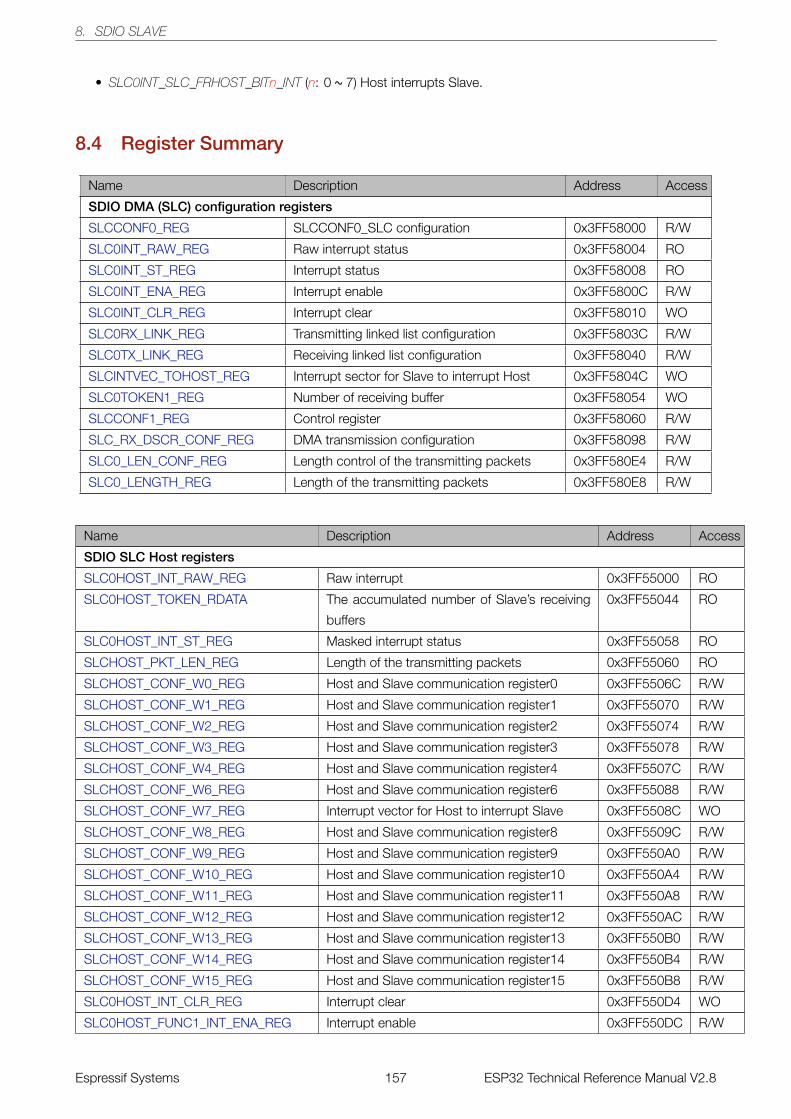
8. SDIO SLAVE
• SLC0INT_SLC_FRHOST_BITn_INT (n: 0 ~ 7) Host interrupts Slave.
8.4 Register Summary
Name Description Address Access
SDIO DMA (SLC) configuration registers
SLCCONF0_REG SLCCONF0_SLC configuration 0x3FF58000 R/W
SLC0INT_RAW_REG Raw interrupt status 0x3FF58004 RO
SLC0INT_ST_REG Interrupt status 0x3FF58008 RO
SLC0INT_ENA_REG Interrupt enable 0x3FF5800C R/W
SLC0INT_CLR_REG Interrupt clear 0x3FF58010 WO
SLC0RX_LINK_REG Transmitting linked list configuration 0x3FF5803C R/W
SLC0TX_LINK_REG Receiving linked list configuration 0x3FF58040 R/W
SLCINTVEC_TOHOST_REG Interrupt sector for Slave to interrupt Host 0x3FF5804C WO
SLC0TOKEN1_REG Number of receiving buffer 0x3FF58054 WO
SLCCONF1_REG Control register 0x3FF58060 R/W
SLC_RX_DSCR_CONF_REG DMA transmission configuration 0x3FF58098 R/W
SLC0_LEN_CONF_REG Length control of the transmitting packets 0x3FF580E4 R/W
SLC0_LENGTH_REG Length of the transmitting packets 0x3FF580E8 R/W
Name Description Address Access
SDIO SLC Host registers
SLC0HOST_INT_RAW_REG Raw interrupt 0x3FF55000 RO
SLC0HOST_TOKEN_RDATA The accumulated number of Slave’s receiving
buffers
0x3FF55044 RO
SLC0HOST_INT_ST_REG Masked interrupt status 0x3FF55058 RO
SLCHOST_PKT_LEN_REG Length of the transmitting packets 0x3FF55060 RO
SLCHOST_CONF_W0_REG Host and Slave communication register0 0x3FF5506C R/W
SLCHOST_CONF_W1_REG Host and Slave communication register1 0x3FF55070 R/W
SLCHOST_CONF_W2_REG Host and Slave communication register2 0x3FF55074 R/W
SLCHOST_CONF_W3_REG Host and Slave communication register3 0x3FF55078 R/W
SLCHOST_CONF_W4_REG Host and Slave communication register4 0x3FF5507C R/W
SLCHOST_CONF_W6_REG Host and Slave communication register6 0x3FF55088 R/W
SLCHOST_CONF_W7_REG Interrupt vector for Host to interrupt Slave 0x3FF5508C WO
SLCHOST_CONF_W8_REG Host and Slave communication register8 0x3FF5509C R/W
SLCHOST_CONF_W9_REG Host and Slave communication register9 0x3FF550A0 R/W
SLCHOST_CONF_W10_REG Host and Slave communication register10 0x3FF550A4 R/W
SLCHOST_CONF_W11_REG Host and Slave communication register11 0x3FF550A8 R/W
SLCHOST_CONF_W12_REG Host and Slave communication register12 0x3FF550AC R/W
SLCHOST_CONF_W13_REG Host and Slave communication register13 0x3FF550B0 R/W
SLCHOST_CONF_W14_REG Host and Slave communication register14 0x3FF550B4 R/W
SLCHOST_CONF_W15_REG Host and Slave communication register15 0x3FF550B8 R/W
SLC0HOST_INT_CLR_REG Interrupt clear 0x3FF550D4 WO
SLC0HOST_FUNC1_INT_ENA_REG Interrupt enable 0x3FF550DC R/W
Espressif Systems 157 ESP32 Technical Reference Manual V2.8
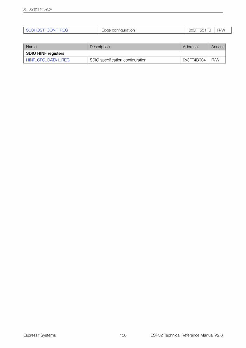
8. SDIO SLAVE
SLCHOST_CONF_REG Edge configuration 0x3FF551F0 R/W
Name Description Address Access
SDIO HINF registers
HINF_CFG_DATA1_REG SDIO specification configuration 0x3FF4B004 R/W
Espressif Systems 158 ESP32 Technical Reference Manual V2.8
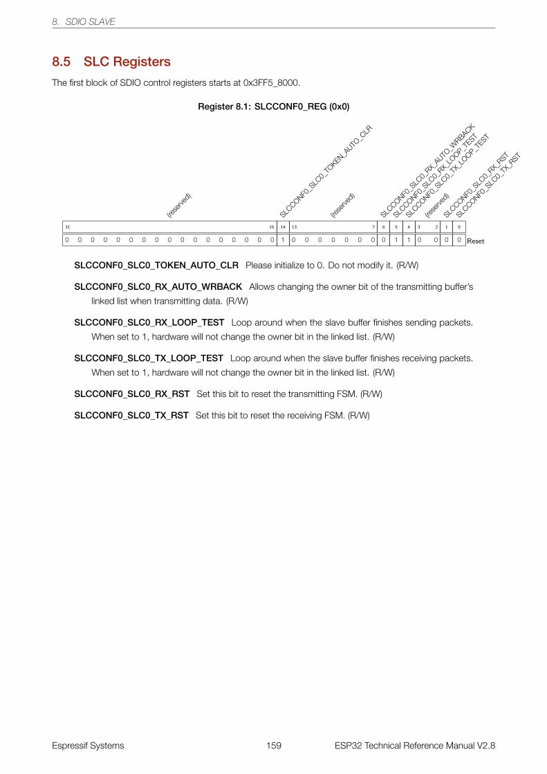
8. SDIO SLAVE
8.5 SLC Registers
The first block of SDIO control registers starts at 0x3FF5_8000.
Register 8.1: SLCCONF0_REG (0x0)
(rese
rved)
0 0 0 0 0 0 0 0 0 0 0 0 0 0 0 0 0
31 15
SLCCONF0
_SLC
0_TO
KEN_AUTO
_CLR
1
14
(rese
rved)
0 0 0 0 0 0 0
13 7
SLCCONF0
_SLC
0_RX_
AUTO_W
RBACK
0
6
SLCCONF0
_SLC
0_RX_
LOOP_T
EST
1
5
SLCCONF0
_SLC
0_TX
_LOOP_T
EST
1
4
(rese
rved)
0 0
3 2
SLCCONF0
_SLC
0_RX_
RST
0
1
SLCCONF0
_SLC
0_TX
_RST
0
0
Reset
SLCCONF0_SLC0_TOKEN_AUTO_CLR Please initialize to 0. Do not modify it. (R/W)
SLCCONF0_SLC0_RX_AUTO_WRBACK Allows changing the owner bit of the transmitting buffer’s
linked list when transmitting data. (R/W)
SLCCONF0_SLC0_RX_LOOP_TEST Loop around when the slave buffer finishes sending packets.
When set to 1, hardware will not change the owner bit in the linked list. (R/W)
SLCCONF0_SLC0_TX_LOOP_TEST Loop around when the slave buffer finishes receiving packets.
When set to 1, hardware will not change the owner bit in the linked list. (R/W)
SLCCONF0_SLC0_RX_RST Set this bit to reset the transmitting FSM. (R/W)
SLCCONF0_SLC0_TX_RST Set this bit to reset the receiving FSM. (R/W)
Espressif Systems 159 ESP32 Technical Reference Manual V2.8
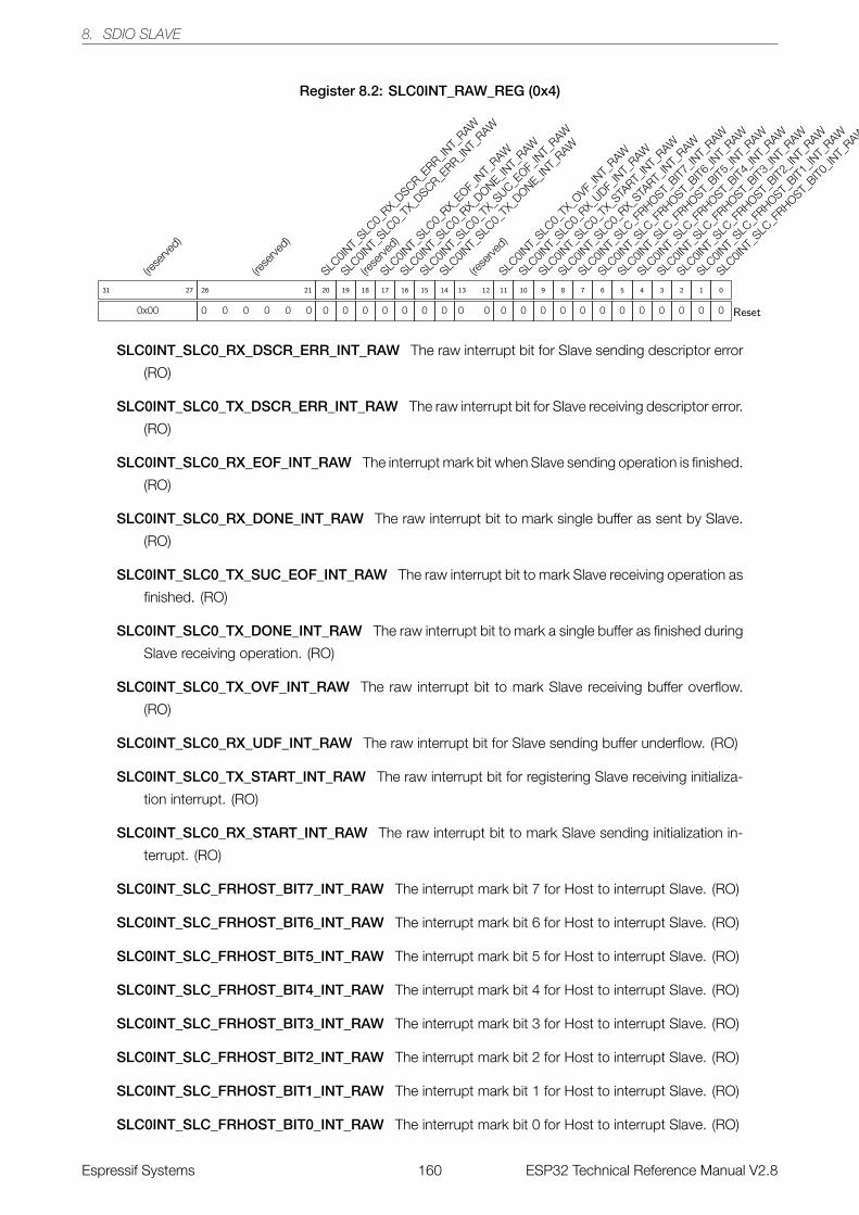
8. SDIO SLAVE
Register 8.2: SLC0INT_RAW_REG (0x4)
(rese
rved)
0x00
31 27
(rese
rved)
0 0 0 0 0 0
26 21
SLC0IN
T_SLC
0_RX_
DSCR_ERR_IN
T_RAW
0
20
SLC0IN
T_SLC
0_TX
_DSCR_E
RR_INT_
RAW
0
19
(rese
rved)
0
18
SLC0IN
T_SLC
0_RX_
EOF_IN
T_RAW
0
17
SLC0IN
T_SLC
0_RX_
DONE_INT_
RAW
0
16
SLC0IN
T_SLC
0_TX
_SUC_E
OF_IN
T_RAW
0
15
SLC0IN
T_SLC
0_TX
_DONE_IN
T_RAW
0
14
(rese
rved)
0 0
13 12
SLC0IN
T_SLC
0_TX
_OVF_
INT_
RAW
0
11
SLC0IN
T_SLC
0_RX_
UDF_IN
T_RAW
0
10
SLC0IN
T_SLC
0_TX
_STA
RT_IN
T_RAW
0
9
SLC0IN
T_SLC
0_RX_
START_
INT_
RAW
0
8
SLC0IN
T_SLC
_FRHOST_
BIT7_IN
T_RAW
0
7
SLC0IN
T_SLC
_FRHOST_
BIT6_IN
T_RAW
0
6
SLC0IN
T_SLC
_FRHOST_
BIT5_IN
T_RAW
0
5
SLC0IN
T_SLC
_FRHOST_
BIT4_IN
T_RAW
0
4
SLC0IN
T_SLC
_FRHOST_
BIT3_IN
T_RAW
0
3
SLC0IN
T_SLC
_FRHOST_
BIT2_IN
T_RAW
0
2
SLC0IN
T_SLC
_FRHOST_
BIT1_IN
T_RAW
0
1
SLC0IN
T_SLC
_FRHOST_
BIT0_IN
T_RAW
0
0
Reset
SLC0INT_SLC0_RX_DSCR_ERR_INT_RAW The raw interrupt bit for Slave sending descriptor error
(RO)
SLC0INT_SLC0_TX_DSCR_ERR_INT_RAW The raw interrupt bit for Slave receiving descriptor error.
(RO)
SLC0INT_SLC0_RX_EOF_INT_RAW The interrupt mark bit when Slave sending operation is finished.
(RO)
SLC0INT_SLC0_RX_DONE_INT_RAW The raw interrupt bit to mark single buffer as sent by Slave.
(RO)
SLC0INT_SLC0_TX_SUC_EOF_INT_RAW The raw interrupt bit to mark Slave receiving operation as
finished. (RO)
SLC0INT_SLC0_TX_DONE_INT_RAW The raw interrupt bit to mark a single buffer as finished during
Slave receiving operation. (RO)
SLC0INT_SLC0_TX_OVF_INT_RAW The raw interrupt bit to mark Slave receiving buffer overflow.
(RO)
SLC0INT_SLC0_RX_UDF_INT_RAW The raw interrupt bit for Slave sending buffer underflow. (RO)
SLC0INT_SLC0_TX_START_INT_RAW The raw interrupt bit for registering Slave receiving initializa-
tion interrupt. (RO)
SLC0INT_SLC0_RX_START_INT_RAW The raw interrupt bit to mark Slave sending initialization in-
terrupt. (RO)
SLC0INT_SLC_FRHOST_BIT7_INT_RAW The interrupt mark bit 7 for Host to interrupt Slave. (RO)
SLC0INT_SLC_FRHOST_BIT6_INT_RAW The interrupt mark bit 6 for Host to interrupt Slave. (RO)
SLC0INT_SLC_FRHOST_BIT5_INT_RAW The interrupt mark bit 5 for Host to interrupt Slave. (RO)
SLC0INT_SLC_FRHOST_BIT4_INT_RAW The interrupt mark bit 4 for Host to interrupt Slave. (RO)
SLC0INT_SLC_FRHOST_BIT3_INT_RAW The interrupt mark bit 3 for Host to interrupt Slave. (RO)
SLC0INT_SLC_FRHOST_BIT2_INT_RAW The interrupt mark bit 2 for Host to interrupt Slave. (RO)
SLC0INT_SLC_FRHOST_BIT1_INT_RAW The interrupt mark bit 1 for Host to interrupt Slave. (RO)
SLC0INT_SLC_FRHOST_BIT0_INT_RAW The interrupt mark bit 0 for Host to interrupt Slave. (RO)
Espressif Systems 160 ESP32 Technical Reference Manual V2.8

8. SDIO SLAVE
Register 8.3: SLC0INT_ST_REG (0x8)
(rese
rved)
0x00
31 27
(rese
rved)
0 0 0 0 0 0
26 21
SLC0IN
T_SLC
0_RX_
DSCR_ERR_IN
T_ST
0
20
SLC0IN
T_SLC
0_TX
_DSCR_E
RR_INT_
ST
0
19
(rese
rved)
0
18
SLC0IN
T_SLC
0_RX_
EOF_IN
T_ST
0
17
SLC0IN
T_SLC
0_RX_
DONE_INT_
ST
0
16
SLC0IN
T_SLC
0_TX
_SUC_E
OF_IN
T_ST
0
15
SLC0IN
T_SLC
0_TX
_DONE_IN
T_ST
0
14
(rese
rved)
0 0
13 12
SLC0IN
T_SLC
0_TX
_OVF_
INT_
ST
0
11
SLC0IN
T_SLC
0_RX_
UDF_IN
T_ST
0
10
SLC0IN
T_SLC
0_TX
_STA
RT_IN
T_ST
0
9
SLC0IN
T_SLC
0_RX_
START_
INT_
ST
0
8
SLC0IN
T_SLC
_FRHOST_
BIT7_IN
T_ST
0
7
SLC0IN
T_SLC
_FRHOST_
BIT6_IN
T_ST
0
6
SLC0IN
T_SLC
_FRHOST_
BIT5_IN
T_ST
0
5
SLC0IN
T_SLC
_FRHOST_
BIT4_IN
T_ST
0
4
SLC0IN
T_SLC
_FRHOST_
BIT3_IN
T_ST
0
3
SLC0IN
T_SLC
_FRHOST_
BIT2_IN
T_ST
0
2
SLC0IN
T_SLC
_FRHOST_
BIT1_IN
T_ST
0
1
SLC0IN
T_SLC
_FRHOST_
BIT0_IN
T_ST
0
0
Reset
SLC0INT_SLC0_RX_DSCR_ERR_INT_ST The interrupt status bit for Slave sending descriptor error.
(RO)
SLC0INT_SLC0_TX_DSCR_ERR_INT_ST The interrupt status bit for Slave receiving descriptor error.
(RO)
SLC0INT_SLC0_RX_EOF_INT_ST The interrupt status bit for finished Slave sending operation. (RO)
SLC0INT_SLC0_RX_DONE_INT_ST The interrupt status bit for finished Slave sending operation.
(RO)
SLC0INT_SLC0_TX_SUC_EOF_INT_ST The interrupt status bit for marking Slave receiving opera-
tion as finished. (RO)
SLC0INT_SLC0_TX_DONE_INT_ST The interrupt status bit for marking a single buffer as finished
during the receiving operation. (RO)
SLC0INT_SLC0_TX_OVF_INT_ST The interrupt status bit for Slave receiving overflow interrupt. (RO)
SLC0INT_SLC0_RX_UDF_INT_ST The interrupt status bit for Slave sending buffer underflow. (RO)
SLC0INT_SLC0_TX_START_INT_ST The interrupt status bit for Slave receiving interrupt initialization.
(RO)
SLC0INT_SLC0_RX_START_INT_ST The interrupt status bit for Slave sending interrupt initialization.
(RO)
SLC0INT_SLC_FRHOST_BIT7_INT_ST The interrupt status bit 7 for Host to interrupt Slave. (RO)
SLC0INT_SLC_FRHOST_BIT6_INT_ST The interrupt status bit 6 for Host to interrupt Slave. (RO)
SLC0INT_SLC_FRHOST_BIT5_INT_ST The interrupt status bit 5 for Host to interrupt Slave. (RO)
SLC0INT_SLC_FRHOST_BIT4_INT_ST The interrupt status bit 4 for Host to interrupt Slave. (RO)
SLC0INT_SLC_FRHOST_BIT3_INT_ST The interrupt status bit 3 for Host to interrupt Slave. (RO)
SLC0INT_SLC_FRHOST_BIT2_INT_ST The interrupt status bit 2 for Host to interrupt Slave. (RO)
SLC0INT_SLC_FRHOST_BIT1_INT_ST The interrupt status bit 1 for Host to interrupt Slave. (RO)
SLC0INT_SLC_FRHOST_BIT0_INT_ST The interrupt status bit 0 for Host to interrupt Slave. (RO)
Espressif Systems 161 ESP32 Technical Reference Manual V2.8
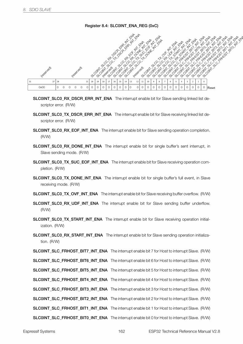
8. SDIO SLAVE
Register 8.4: SLC0INT_ENA_REG (0xC)
(rese
rved)
0x00
31 27
(rese
rved)
0 0 0 0 0 0
26 21
SLC0IN
T_SLC
0_RX_
DSCR_ERR_IN
T_ENA
0
20
SLC0IN
T_SLC
0_TX
_DSCR_E
RR_INT_
ENA
0
19
(rese
rved)
0
18
SLC0IN
T_SLC
0_RX_
EOF_IN
T_ENA
0
17
SLC0IN
T_SLC
0_RX_
DONE_INT_
ENA
0
16
SLC0IN
T_SLC
0_TX
_SUC_E
OF_IN
T_ENA
0
15
SLC0IN
T_SLC
0_TX
_DONE_IN
T_ENA
0
14
(rese
rved)
0 0
13 12
SLC0IN
T_SLC
0_TX
_OVF_
INT_
ENA
0
11
SLC0IN
T_SLC
0_RX_
UDF_IN
T_ENA
0
10
SLC0IN
T_SLC
0_TX
_STA
RT_IN
T_ENA
0
9
SLC0IN
T_SLC
0_RX_
START_
INT_
ENA
0
8
SLC0IN
T_SLC
_FRHOST_
BIT7_IN
T_ENA
0
7
SLC0IN
T_SLC
_FRHOST_
BIT6_IN
T_ENA
0
6
SLC0IN
T_SLC
_FRHOST_
BIT5_IN
T_ENA
0
5
SLC0IN
T_SLC
_FRHOST_
BIT4_IN
T_ENA
0
4
SLC0IN
T_SLC
_FRHOST_
BIT3_IN
T_ENA
0
3
SLC0IN
T_SLC
_FRHOST_
BIT2_IN
T_ENA
0
2
SLC0IN
T_SLC
_FRHOST_
BIT1_IN
T_ENA
0
1
SLC0IN
T_SLC
_FRHOST_
BIT0_IN
T_ENA
0
0
Reset
SLC0INT_SLC0_RX_DSCR_ERR_INT_ENA The interrupt enable bit for Slave sending linked list de-
scriptor error. (R/W)
SLC0INT_SLC0_TX_DSCR_ERR_INT_ENA The interrupt enable bit for Slave receiving linked list de-
scriptor error. (R/W)
SLC0INT_SLC0_RX_EOF_INT_ENA The interrupt enable bit for Slave sending operation completion.
(R/W)
SLC0INT_SLC0_RX_DONE_INT_ENA The interrupt enable bit for single buffer’s sent interrupt, in
Slave sending mode. (R/W)
SLC0INT_SLC0_TX_SUC_EOF_INT_ENA The interrupt enable bit for Slave receiving operation com-
pletion. (R/W)
SLC0INT_SLC0_TX_DONE_INT_ENA The interrupt enable bit for single buffer’s full event, in Slave
receiving mode. (R/W)
SLC0INT_SLC0_TX_OVF_INT_ENA The interrupt enable bit for Slave receiving buffer overflow. (R/W)
SLC0INT_SLC0_RX_UDF_INT_ENA The interrupt enable bit for Slave sending buffer underflow.
(R/W)
SLC0INT_SLC0_TX_START_INT_ENA The interrupt enable bit for Slave receiving operation initial-
ization. (R/W)
SLC0INT_SLC0_RX_START_INT_ENA The interrupt enable bit for Slave sending operation initializa-
tion. (R/W)
SLC0INT_SLC_FRHOST_BIT7_INT_ENA The interrupt enable bit 7 for Host to interrupt Slave. (R/W)
SLC0INT_SLC_FRHOST_BIT6_INT_ENA The interrupt enable bit 6 for Host to interrupt Slave. (R/W)
SLC0INT_SLC_FRHOST_BIT5_INT_ENA The interrupt enable bit 5 for Host to interrupt Slave. (R/W)
SLC0INT_SLC_FRHOST_BIT4_INT_ENA The interrupt enable bit 4 for Host to interrupt Slave. (R/W)
SLC0INT_SLC_FRHOST_BIT3_INT_ENA The interrupt enable bit 3 for Host to interrupt Slave. (R/W)
SLC0INT_SLC_FRHOST_BIT2_INT_ENA The interrupt enable bit 2 for Host to interrupt Slave. (R/W)
SLC0INT_SLC_FRHOST_BIT1_INT_ENA The interrupt enable bit 1 for Host to interrupt Slave. (R/W)
SLC0INT_SLC_FRHOST_BIT0_INT_ENA The interrupt enable bit 0 for Host to interrupt Slave. (R/W)
Espressif Systems 162 ESP32 Technical Reference Manual V2.8

8. SDIO SLAVE
Register 8.5: SLC0INT_CLR_REG (0x10)
(rese
rved)
0x00
31 27
(rese
rved)
0 0 0 0 0 0
26 21
SLC0IN
T_SLC
0_RX_
DSCR_ERR_IN
T_CLR
0
20
SLC0IN
T_SLC
0_TX
_DSCR_E
RR_INT_
CLR
0
19
(rese
rved)
0
18
SLC0IN
T_SLC
0_RX_
EOF_IN
T_CLR
0
17
SLC0IN
T_SLC
0_RX_
DONE_INT_
CLR
0
16
SLC0IN
T_SLC
0_TX
_SUC_E
OF_IN
T_CLR
0
15
SLC0IN
T_SLC
0_TX
_DONE_IN
T_CLR
0
14
(rese
rved)
0 0
13 12
SLC0IN
T_SLC
0_TX
_OVF_
INT_
CLR
0
11
SLC0IN
T_SLC
0_RX_
UDF_IN
T_CLR
0
10
SLC0IN
T_SLC
0_TX
_STA
RT_IN
T_CLR
0
9
SLC0IN
T_SLC
0_RX_
START_
INT_
CLR
0
8
SLC0IN
T_SLC
_FRHOST_
BIT7_IN
T_CLR
0
7
SLC0IN
T_SLC
_FRHOST_
BIT6_IN
T_CLR
0
6
SLC0IN
T_SLC
_FRHOST_
BIT5_IN
T_CLR
0
5
SLC0IN
T_SLC
_FRHOST_
BIT4_IN
T_CLR
0
4
SLC0IN
T_SLC
_FRHOST_
BIT3_IN
T_CLR
0
3
SLC0IN
T_SLC
_FRHOST_
BIT2_IN
T_CLR
0
2
SLC0IN
T_SLC
_FRHOST_
BIT1_IN
T_CLR
0
1
SLC0IN
T_SLC
_FRHOST_
BIT0_IN
T_CLR
0
0
Reset
SLC0INT_SLC0_RX_DSCR_ERR_INT_CLR Interrupt clear bit for Slave sending linked list descriptor error. (WO)
SLC0INT_SLC0_TX_DSCR_ERR_INT_CLR Interrupt clear bit for Slave receiving linked list descriptor error. (WO)
SLC0INT_SLC0_RX_EOF_INT_CLR Interrupt clear bit for Slave sending operation completion. (WO)
SLC0INT_SLC0_RX_DONE_INT_CLR Interrupt clear bit for single buffer’s sent interrupt, in Slave sending mode. (WO)
SLC0INT_SLC0_TX_SUC_EOF_INT_CLR Interrupt clear bit for Slave receiving operation completion. (WO)
SLC0INT_SLC0_TX_DONE_INT_CLR Interrupt clear bit for single buffer’s full event, in Slave receiving mode. (WO)
SLC0INT_SLC0_TX_OVF_INT_CLR Set this bit to clear the Slave receiving overflow interrupt. (WO)
SLC0INT_SLC0_RX_UDF_INT_CLR Set this bit to clear the Slave sending underflow interrupt. (WO)
SLC0INT_SLC0_TX_START_INT_CLR Set this bit to clear the interrupt for Slave receiving operation initialization. (WO)
SLC0INT_SLC0_RX_START_INT_CLR Set this bit to clear the interrupt for Slave sending operation initialization. (WO)
SLC0INT_SLC_FRHOST_BIT7_INT_CLR Set this bit to clear the SLC0INT_SLC_FRHOST_BIT7_INT interrupt. (WO)
SLC0INT_SLC_FRHOST_BIT6_INT_CLR Set this bit to clear the SLC0INT_SLC_FRHOST_BIT6_INT interrupt. (WO)
SLC0INT_SLC_FRHOST_BIT5_INT_CLR Set this bit to clear the SLC0INT_SLC_FRHOST_BIT5_INT interrupt. (WO)
SLC0INT_SLC_FRHOST_BIT4_INT_CLR Set this bit to clear the SLC0INT_SLC_FRHOST_BIT4_INT interrupt. (WO)
SLC0INT_SLC_FRHOST_BIT3_INT_CLR Set this bit to clear the SLC0INT_SLC_FRHOST_BIT3_INT interrupt. (WO)
SLC0INT_SLC_FRHOST_BIT2_INT_CLR Set this bit to clear the SLC0INT_SLC_FRHOST_BIT2_INT interrupt. (WO)
SLC0INT_SLC_FRHOST_BIT1_INT_CLR Set this bit to clear the SLC0INT_SLC_FRHOST_BIT1_INT interrupt. (WO)
SLC0INT_SLC_FRHOST_BIT0_INT_CLR Set this bit to clear the SLC0INT_SLC_FRHOST_BIT0_INT interrupt. (WO)
Espressif Systems 163 ESP32 Technical Reference Manual V2.8
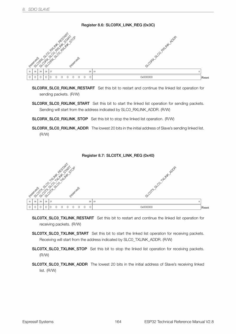
8. SDIO SLAVE
Register 8.6: SLC0RX_LINK_REG (0x3C)
(rese
rved)
0
31
SLC0R
X_SLC
0_RXL
INK_R
ESTART
0
30
SLC0R
X_SLC
0_RXL
INK_S
TART
0
29
SLC0R
X_SLC
0_RXL
INK_S
TOP
0
28
(rese
rved)
0 0 0 0 0 0 0 0
27 20
SLC0R
X_SLC
0_RXL
INK_A
DDR
0x000000
19 0
Reset
SLC0RX_SLC0_RXLINK_RESTART Set this bit to restart and continue the linked list operation for
sending packets. (R/W)
SLC0RX_SLC0_RXLINK_START Set this bit to start the linked list operation for sending packets.
Sending will start from the address indicated by SLC0_RXLINK_ADDR. (R/W)
SLC0RX_SLC0_RXLINK_STOP Set this bit to stop the linked list operation. (R/W)
SLC0RX_SLC0_RXLINK_ADDR The lowest 20 bits in the initial address of Slave’s sending linked list.
(R/W)
Register 8.7: SLC0TX_LINK_REG (0x40)
(rese
rved)
0
31
SLC0T
X_SLC
0_TX
LINK_R
ESTART
0
30
SLC0T
X_SLC
0_TX
LINK_S
TART
0
29
SLC0T
X_SLC
0_TX
LINK_S
TOP
0
28
(rese
rved)
0 0 0 0 0 0 0 0
27 20
SLC0T
X_SLC
0_TX
LINK_A
DDR
0x000000
19 0
Reset
SLC0TX_SLC0_TXLINK_RESTART Set this bit to restart and continue the linked list operation for
receiving packets. (R/W)
SLC0TX_SLC0_TXLINK_START Set this bit to start the linked list operation for receiving packets.
Receiving will start from the address indicated by SLC0_TXLINK_ADDR. (R/W)
SLC0TX_SLC0_TXLINK_STOP Set this bit to stop the linked list operation for receiving packets.
(R/W)
SLC0TX_SLC0_TXLINK_ADDR The lowest 20 bits in the initial address of Slave’s receiving linked
list. (R/W)
Espressif Systems 164 ESP32 Technical Reference Manual V2.8
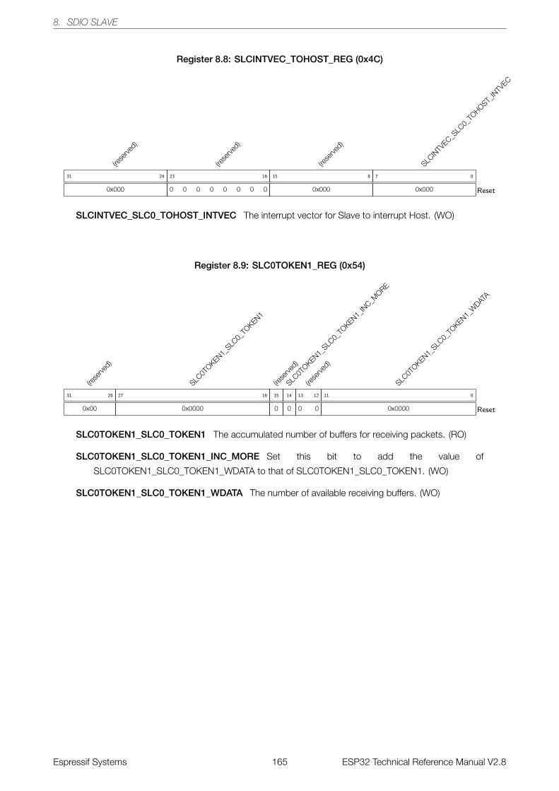
8. SDIO SLAVE
Register 8.8: SLCINTVEC_TOHOST_REG (0x4C)
(rese
rved)
0x000
31 24
(rese
rved)
0 0 0 0 0 0 0 0
23 16
(rese
rved)
0x000
15 8
SLCIN
TVEC_S
LC0_
TOHOST_
INTV
EC
0x000
7 0
Reset
SLCINTVEC_SLC0_TOHOST_INTVEC The interrupt vector for Slave to interrupt Host. (WO)
Register 8.9: SLC0TOKEN1_REG (0x54)
(rese
rved)
0x00
31 28
SLC0T
OKEN1_SLC
0_TO
KEN1
0x0000
27 16
(rese
rved)
0
15
SLC0T
OKEN1_SLC
0_TO
KEN1_IN
C_MORE
0
14
(rese
rved)
0 0
13 12
SLC0T
OKEN1_SLC
0_TO
KEN1_W
DATA
0x0000
11 0
Reset
SLC0TOKEN1_SLC0_TOKEN1 The accumulated number of buffers for receiving packets. (RO)
SLC0TOKEN1_SLC0_TOKEN1_INC_MORE Set this bit to add the value of
SLC0TOKEN1_SLC0_TOKEN1_WDATA to that of SLC0TOKEN1_SLC0_TOKEN1. (WO)
SLC0TOKEN1_SLC0_TOKEN1_WDATA The number of available receiving buffers. (WO)
Espressif Systems 165 ESP32 Technical Reference Manual V2.8
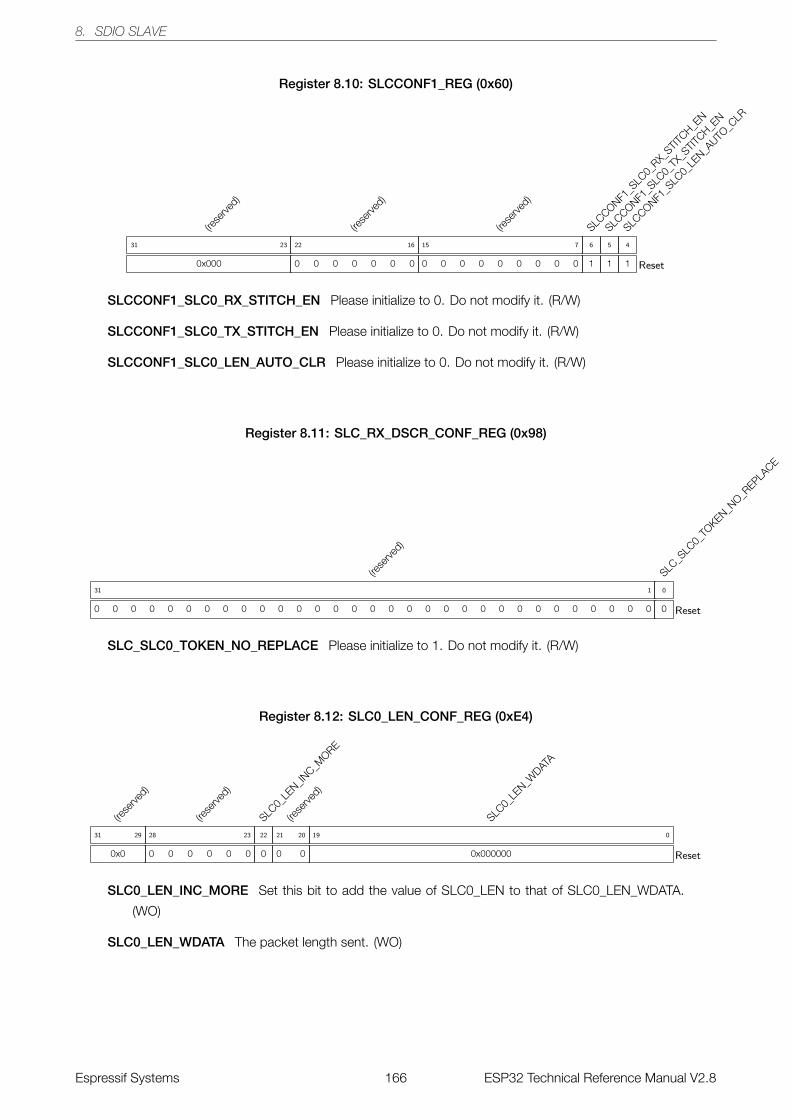
8. SDIO SLAVE
Register 8.10: SLCCONF1_REG (0x60)
(rese
rved)
0x000
31 23
(rese
rved)
0 0 0 0 0 0 0
22 16
(rese
rved)
0 0 0 0 0 0 0 0 0
15 7
SLCCONF1
_SLC
0_RX_
STITCH_E
N
1
6
SLCCONF1
_SLC
0_TX
_STIT
CH_EN
1
5
SLCCONF1
_SLC
0_LE
N_AUTO
_CLR
1
4
Reset
SLCCONF1_SLC0_RX_STITCH_EN Please initialize to 0. Do not modify it. (R/W)
SLCCONF1_SLC0_TX_STITCH_EN Please initialize to 0. Do not modify it. (R/W)
SLCCONF1_SLC0_LEN_AUTO_CLR Please initialize to 0. Do not modify it. (R/W)
Register 8.11: SLC_RX_DSCR_CONF_REG (0x98)
(rese
rved)
0 0 0 0 0 0 0 0 0 0 0 0 0 0 0 0 0 0 0 0 0 0 0 0 0 0 0 0 0 0 0
31 1
SLC_S
LC0_
TOKEN_N
O_REPLA
CE
0
0
Reset
SLC_SLC0_TOKEN_NO_REPLACE Please initialize to 1. Do not modify it. (R/W)
Register 8.12: SLC0_LEN_CONF_REG (0xE4)
(rese
rved)
0x0
31 29
(rese
rved)
0 0 0 0 0 0
28 23
SLC0_
LEN_IN
C_MORE
0
22
(rese
rved)
0 0
21 20
SLC0_
LEN_W
DATA
0x000000
19 0
Reset
SLC0_LEN_INC_MORE Set this bit to add the value of SLC0_LEN to that of SLC0_LEN_WDATA.
(WO)
SLC0_LEN_WDATA The packet length sent. (WO)
Espressif Systems 166 ESP32 Technical Reference Manual V2.8
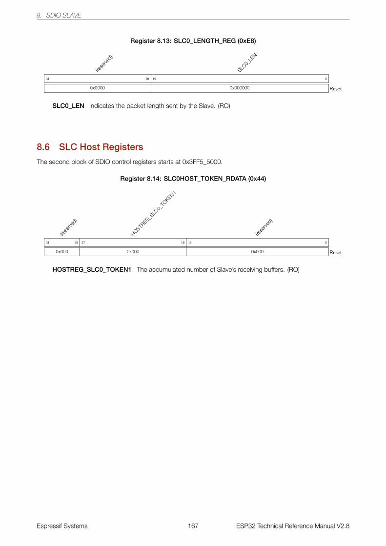
8. SDIO SLAVE
Register 8.13: SLC0_LENGTH_REG (0xE8)
(rese
rved)
0x0000
31 20
SLC0_
LEN
0x000000
19 0
Reset
SLC0_LEN Indicates the packet length sent by the Slave. (RO)
8.6 SLC Host Registers
The second block of SDIO control registers starts at 0x3FF5_5000.
Register 8.14: SLC0HOST_TOKEN_RDATA (0x44)
(rese
rved)
0x000
31 28
HOSTREG_S
LC0_
TOKEN1
0x000
27 16
(rese
rved)
0x000
15 0
Reset
HOSTREG_SLC0_TOKEN1 The accumulated number of Slave’s receiving buffers. (RO)
Espressif Systems 167 ESP32 Technical Reference Manual V2.8

8. SDIO SLAVE
Register 8.15: SLC0HOST_INT_RAW_REG (0x50)
(rese
rved)
0x00
31 26
(rese
rved)
0 0
25 24
SLC0H
OST_SLC
0_RX_
NEW_P
ACKET_IN
T_RAW
0
23
(rese
rved)
0 0 0 0 0
22 18
SLC0H
OST_SLC
0_TX
_OVF_
INT_
RAW
0
17
SLC0H
OST_SLC
0_RX_
UDF_IN
T_RAW
0
16
(rese
rved)
0 0 0 0 0 0 0 0
15 8
SLC0H
OST_SLC
0_TO
HOST_BIT7
_INT_
RAW
0
7
SLC0H
OST_SLC
0_TO
HOST_BIT6
_INT_
RAW
0
6
SLC0H
OST_SLC
0_TO
HOST_BIT5
_INT_
RAW
0
5
SLC0H
OST_SLC
0_TO
HOST_BIT4
_INT_
RAW
0
4
SLC0H
OST_SLC
0_TO
HOST_BIT3
_INT_
RAW
0
3
SLC0H
OST_SLC
0_TO
HOST_BIT2
_INT_
RAW
0
2
SLC0H
OST_SLC
0_TO
HOST_BIT1
_INT_
RAW
0
1
SLC0H
OST_SLC
0_TO
HOST_BIT0
_INT_
RAW
0
0
Reset
SLC0HOST_SLC0_RX_NEW_PACKET_INT_RAW The raw interrupt status bit for the
SLC0HOST_SLC0_RX_NEW_PACKET_INT interrupt. (RO)
SLC0HOST_SLC0_TX_OVF_INT_RAW The raw interrupt status bit for the
SLC0HOST_SLC0_TX_OVF_INT interrupt. (RO)
SLC0HOST_SLC0_RX_UDF_INT_RAW The raw interrupt status bit for the
SLC0HOST_SLC0_RX_UDF_INT interrupt. (RO)
SLC0HOST_SLC0_TOHOST_BIT7_INT_RAW The raw interrupt status bit for the
SLC0HOST_SLC0_TOHOST_BIT7_INT interrupt. (RO)
SLC0HOST_SLC0_TOHOST_BIT6_INT_RAW The raw interrupt status bit for the
SLC0HOST_SLC0_TOHOST_BIT6_INT interrupt. (RO)
SLC0HOST_SLC0_TOHOST_BIT5_INT_RAW The raw interrupt status bit for the
SLC0HOST_SLC0_TOHOST_BIT5_INT interrupt. (RO)
SLC0HOST_SLC0_TOHOST_BIT4_INT_RAW The raw interrupt status bit for the
SLC0HOST_SLC0_TOHOST_BIT4_INT interrupt. (RO)
SLC0HOST_SLC0_TOHOST_BIT3_INT_RAW The raw interrupt status bit for the
SLC0HOST_SLC0_TOHOST_BIT3_INT interrupt. (RO)
SLC0HOST_SLC0_TOHOST_BIT2_INT_RAW The raw interrupt status bit for the
SLC0HOST_SLC0_TOHOST_BIT2_INT interrupt. (RO)
SLC0HOST_SLC0_TOHOST_BIT1_INT_RAW The raw interrupt status bit for the
SLC0HOST_SLC0_TOHOST_BIT1_INT interrupt. (RO)
SLC0HOST_SLC0_TOHOST_BIT0_INT_RAW The raw interrupt status bit for the
SLC0HOST_SLC0_TOHOST_BIT0_INT interrupt. (RO)
Espressif Systems 168 ESP32 Technical Reference Manual V2.8
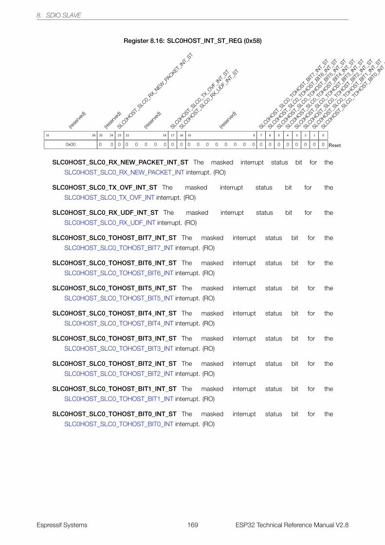
8. SDIO SLAVE
Register 8.16: SLC0HOST_INT_ST_REG (0x58)
(rese
rved)
0x00
31 26
(rese
rved)
0 0
25 24
SLC0H
OST_SLC
0_RX_
NEW_P
ACKET_IN
T_ST
0
23
(rese
rved)
0 0 0 0 0
22 18
SLC0H
OST_SLC
0_TX
_OVF_
INT_
ST
0
17
SLC0H
OST_SLC
0_RX_
UDF_IN
T_ST
0
16
(rese
rved)
0 0 0 0 0 0 0 0
15 8
SLC0H
OST_SLC
0_TO
HOST_BIT7
_INT_
ST
0
7
SLC0H
OST_SLC
0_TO
HOST_BIT6
_INT_
ST
0
6
SLC0H
OST_SLC
0_TO
HOST_BIT5
_INT_
ST
0
5
SLC0H
OST_SLC
0_TO
HOST_BIT4
_INT_
ST
0
4
SLC0H
OST_SLC
0_TO
HOST_BIT3
_INT_
ST
0
3
SLC0H
OST_SLC
0_TO
HOST_BIT2
_INT_
ST
0
2
SLC0H
OST_SLC
0_TO
HOST_BIT1
_INT_
ST
0
1
SLC0H
OST_SLC
0_TO
HOST_BIT0
_INT_
ST
0
0
Reset
SLC0HOST_SLC0_RX_NEW_PACKET_INT_ST The masked interrupt status bit for the
SLC0HOST_SLC0_RX_NEW_PACKET_INT interrupt. (RO)
SLC0HOST_SLC0_TX_OVF_INT_ST The masked interrupt status bit for the
SLC0HOST_SLC0_TX_OVF_INT interrupt. (RO)
SLC0HOST_SLC0_RX_UDF_INT_ST The masked interrupt status bit for the
SLC0HOST_SLC0_RX_UDF_INT interrupt. (RO)
SLC0HOST_SLC0_TOHOST_BIT7_INT_ST The masked interrupt status bit for the
SLC0HOST_SLC0_TOHOST_BIT7_INT interrupt. (RO)
SLC0HOST_SLC0_TOHOST_BIT6_INT_ST The masked interrupt status bit for the
SLC0HOST_SLC0_TOHOST_BIT6_INT interrupt. (RO)
SLC0HOST_SLC0_TOHOST_BIT5_INT_ST The masked interrupt status bit for the
SLC0HOST_SLC0_TOHOST_BIT5_INT interrupt. (RO)
SLC0HOST_SLC0_TOHOST_BIT4_INT_ST The masked interrupt status bit for the
SLC0HOST_SLC0_TOHOST_BIT4_INT interrupt. (RO)
SLC0HOST_SLC0_TOHOST_BIT3_INT_ST The masked interrupt status bit for the
SLC0HOST_SLC0_TOHOST_BIT3_INT interrupt. (RO)
SLC0HOST_SLC0_TOHOST_BIT2_INT_ST The masked interrupt status bit for the
SLC0HOST_SLC0_TOHOST_BIT2_INT interrupt. (RO)
SLC0HOST_SLC0_TOHOST_BIT1_INT_ST The masked interrupt status bit for the
SLC0HOST_SLC0_TOHOST_BIT1_INT interrupt. (RO)
SLC0HOST_SLC0_TOHOST_BIT0_INT_ST The masked interrupt status bit for the
SLC0HOST_SLC0_TOHOST_BIT0_INT interrupt. (RO)
Espressif Systems 169 ESP32 Technical Reference Manual V2.8
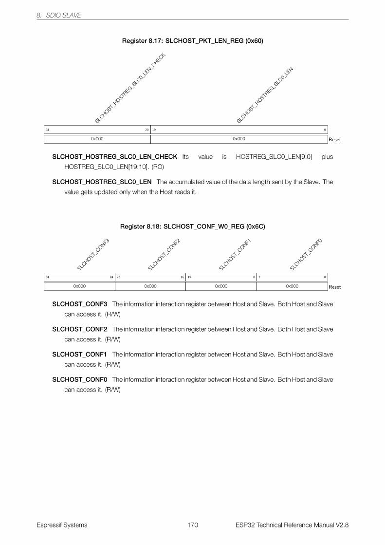
8. SDIO SLAVE
Register 8.17: SLCHOST_PKT_LEN_REG (0x60)
SLCHOST_
HOSTREG_S
LC0_
LEN_C
HECK
0x000
31 20
SLCHOST_
HOSTREG_S
LC0_
LEN
0x000
19 0
Reset
SLCHOST_HOSTREG_SLC0_LEN_CHECK Its value is HOSTREG_SLC0_LEN[9:0] plus
HOSTREG_SLC0_LEN[19:10]. (RO)
SLCHOST_HOSTREG_SLC0_LEN The accumulated value of the data length sent by the Slave. The
value gets updated only when the Host reads it.
Register 8.18: SLCHOST_CONF_W0_REG (0x6C)
SLCHOST_
CONF3
0x000
31 24
SLCHOST_
CONF2
0x000
23 16
SLCHOST_
CONF1
0x000
15 8
SLCHOST_
CONF0
0x000
7 0
Reset
SLCHOST_CONF3 The information interaction register between Host and Slave. Both Host and Slave
can access it. (R/W)
SLCHOST_CONF2 The information interaction register between Host and Slave. Both Host and Slave
can access it. (R/W)
SLCHOST_CONF1 The information interaction register between Host and Slave. Both Host and Slave
can access it. (R/W)
SLCHOST_CONF0 The information interaction register between Host and Slave. Both Host and Slave
can access it. (R/W)
Espressif Systems 170 ESP32 Technical Reference Manual V2.8
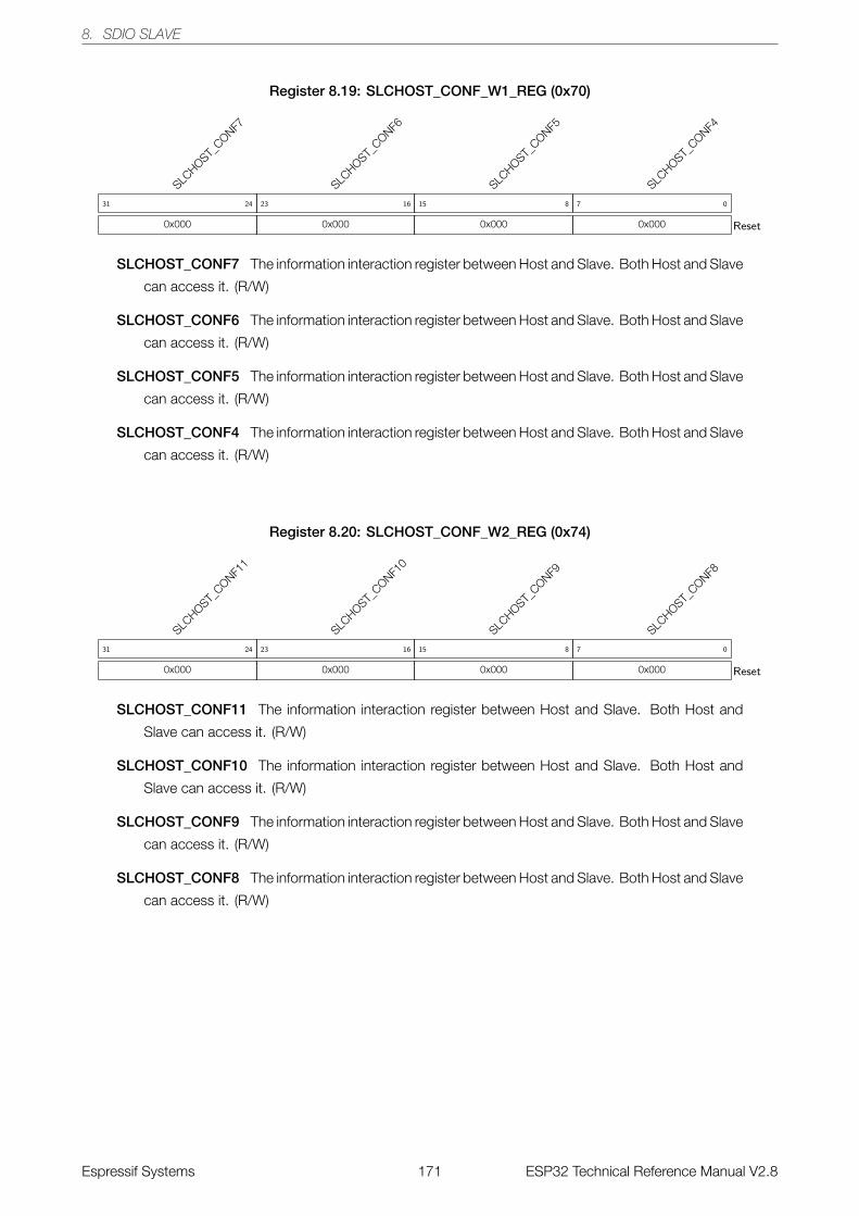
8. SDIO SLAVE
Register 8.19: SLCHOST_CONF_W1_REG (0x70)
SLCHOST_
CONF7
0x000
31 24
SLCHOST_
CONF6
0x000
23 16
SLCHOST_
CONF5
0x000
15 8
SLCHOST_
CONF4
0x000
7 0
Reset
SLCHOST_CONF7 The information interaction register between Host and Slave. Both Host and Slave
can access it. (R/W)
SLCHOST_CONF6 The information interaction register between Host and Slave. Both Host and Slave
can access it. (R/W)
SLCHOST_CONF5 The information interaction register between Host and Slave. Both Host and Slave
can access it. (R/W)
SLCHOST_CONF4 The information interaction register between Host and Slave. Both Host and Slave
can access it. (R/W)
Register 8.20: SLCHOST_CONF_W2_REG (0x74)
SLCHOST_
CONF11
0x000
31 24
SLCHOST_
CONF10
0x000
23 16
SLCHOST_
CONF9
0x000
15 8
SLCHOST_
CONF8
0x000
7 0
Reset
SLCHOST_CONF11 The information interaction register between Host and Slave. Both Host and
Slave can access it. (R/W)
SLCHOST_CONF10 The information interaction register between Host and Slave. Both Host and
Slave can access it. (R/W)
SLCHOST_CONF9 The information interaction register between Host and Slave. Both Host and Slave
can access it. (R/W)
SLCHOST_CONF8 The information interaction register between Host and Slave. Both Host and Slave
can access it. (R/W)
Espressif Systems 171 ESP32 Technical Reference Manual V2.8
8. SDIO SLAVE
Register 8.21: SLCHOST_CONF_W3_REG (0x78)
SLCHOST_
CONF15
0x000
31 24
SLCHOST_
CONF14
0x000
23 16
Reset
SLCHOST_CONF15 The information interaction register between Host and Slave. Both Host and
Slave can be read from and written to this. (R/W)
SLCHOST_CONF14 The information interaction register between Host and Slave. Both Host and
Slave can be read from and written to this. (R/W)
Register 8.22: SLCHOST_CONF_W4_REG (0x7C)
SLCHOST_
CONF19
0x000
31 24
SLCHOST_
CONF18
0x000
23 16
Reset
SLCHOST_CONF19 The information interaction register between Host and Slave. Both Host and
Slave can access it. (R/W)
SLCHOST_CONF18 The information interaction register between Host and Slave. Both Host and
Slave can access it. (R/W)
Espressif Systems 172 ESP32 Technical Reference Manual V2.8
8. SDIO SLAVE
Register 8.23: SLCHOST_CONF_W6_REG (0x88)
SLCHOST_
CONF27
0x000
31 24
SLCHOST_
CONF26
0x000
23 16
SLCHOST_
CONF25
0x000
15 8
SLCHOST_
CONF24
0x000
7 0
Reset
SLCHOST_CONF27 The information interaction register between Host and Slave. Both Host and
Slave can access it. (R/W)
SLCHOST_CONF26 The information interaction register between Host and Slave. Both Host and
Slave can access it. (R/W)
SLCHOST_CONF25 The information interaction register between Host and Slave. Both Host and
Slave can access it. (R/W)
SLCHOST_CONF24 The information interaction register between Host and Slave. Both Host and
Slave can access it. (R/W)
Register 8.24: SLCHOST_CONF_W7_REG (0x8C)
SLCHOST_
CONF31
0 0 0 0 0 0 0 0
31 24
(rese
rved)
0x000
23 16
SLCHOST_
CONF29
0 0 0 0 0 0 0 0
15 8
(rese
rved)
0x000
7 0
Reset
SLCHOST_CONF31 The interrupt vector used by Host to interrupt Slave. This bit will not be cleared
automatically. (WO)
SLCHOST_CONF29 The interrupt vector used by Host to interrupt Slave. This bit will not be cleared
automatically. (WO)
Espressif Systems 173 ESP32 Technical Reference Manual V2.8
8. SDIO SLAVE
Register 8.25: SLCHOST_CONF_W8_REG (0x9C)
SLCHOST_
CONF35
0x000
31 24
SLCHOST_
CONF34
0x000
23 16
SLCHOST_
CONF33
0x000
15 8
SLCHOST_
CONF32
0x000
7 0
Reset
SLCHOST_CONF35 The information interaction register between Host and Slave. Both Host and
Slave can access it. (R/W)
SLCHOST_CONF34 The information interaction register between Host and Slave. Both Host and
Slave can access it. (R/W)
SLCHOST_CONF33 The information interaction register between Host and Slave. Both Host and
Slave can access it. (R/W)
SLCHOST_CONF32 The information interaction register between Host and Slave. Both Host and
Slave can access it. (R/W)
Register 8.26: SLCHOST_CONF_W9_REG (0xA0)
SLCHOST_
CONF39
0x000
31 24
SLCHOST_
CONF38
0x000
23 16
SLCHOST_
CONF37
0x000
15 8
SLCHOST_
CONF36
0x000
7 0
Reset
SLCHOST_CONF39 The information interaction register between Host and Slave. Both Host and
Slave can access it. (R/W)
SLCHOST_CONF38 The information interaction register between Host and Slave. Both Host and
Slave can access it. (R/W)
SLCHOST_CONF37 The information interaction register between Host and Slave. Both Host and
Slave can access it. (R/W)
SLCHOST_CONF36 The information interaction register between Host and Slave. Both Host and
Slave can access it. (R/W)
Espressif Systems 174 ESP32 Technical Reference Manual V2.8

8. SDIO SLAVE
Register 8.27: SLCHOST_CONF_W10_REG (0xA4)
SLCHOST_
CONF43
0x000
31 24
SLCHOST_
CONF42
0x000
23 16
SLCHOST_
CONF41
0x000
15 8
SLCHOST_
CONF40
0x000
7 0
Reset
SLCHOST_CONF43 The information interaction register between Host and Slave. Both Host and
Slave can access it. (R/W)
SLCHOST_CONF42 The information interaction register between Host and Slave. Both Host and
Slave can access it. (R/W)
SLCHOST_CONF41 The information interaction register between Host and Slave. Both Host and
Slave can access it. (R/W)
SLCHOST_CONF40 The information interaction register between Host and Slave. Both Host and
Slave can access it. (R/W)
Register 8.28: SLCHOST_CONF_W11_REG (0xA8)
SLCHOST_
CONF47
0x000
31 24
SLCHOST_
CONF46
0x000
23 16
SLCHOST_
CONF45
0x000
15 8
SLCHOST_
CONF44
0x000
7 0
Reset
SLCHOST_CONF47 The information interaction register between Host and Slave. Both Host and
Slave can access it. (R/W)
SLCHOST_CONF46 The information interaction register between Host and Slave. Both Host and
Slave can access it. (R/W)
SLCHOST_CONF45 The information interaction register between Host and Slave. Both Host and
Slave can access it. (R/W)
SLCHOST_CONF44 The information interaction register between Host and Slave. Both Host and
Slave can access it. (R/W)
Espressif Systems 175 ESP32 Technical Reference Manual V2.8
8. SDIO SLAVE
Register 8.29: SLCHOST_CONF_W12_REG (0xAC)
SLCHOST_
CONF51
0x000
31 24
SLCHOST_
CONF50
0x000
23 16
SLCHOST_
CONF49
0x000
15 8
SLCHOST_
CONF48
0x000
7 0
Reset
SLCHOST_CONF51 The information interaction register between Host and Slave. Both Host and
Slave can access it. (R/W)
SLCHOST_CONF50 The information interaction register between Host and Slave. Both Host and
Slave can access it. (R/W)
SLCHOST_CONF49 The information interaction register between Host and Slave. Both Host and
Slave can access it. (R/W)
SLCHOST_CONF48 The information interaction register between Host and Slave. Both Host and
Slave can access it. (R/W)
Register 8.30: SLCHOST_CONF_W13_REG (0xB0)
SLCHOST_
CONF55
0x000
31 24
SLCHOST_
CONF54
0x000
23 16
SLCHOST_
CONF53
0x000
15 8
SLCHOST_
CONF52
0x000
7 0
Reset
SLCHOST_CONF55 The information interaction register between Host and Slave. Both Host and
Slave can access it. (R/W)
SLCHOST_CONF54 The information interaction register between Host and Slave. Both Host and
Slave can access it. (R/W)
SLCHOST_CONF53 The information interaction register between Host and Slave. Both Host and
Slave can access it. (R/W)
SLCHOST_CONF52 The information interaction register between Host and Slave. Both Host and
Slave can access it. (R/W)
Espressif Systems 176 ESP32 Technical Reference Manual V2.8
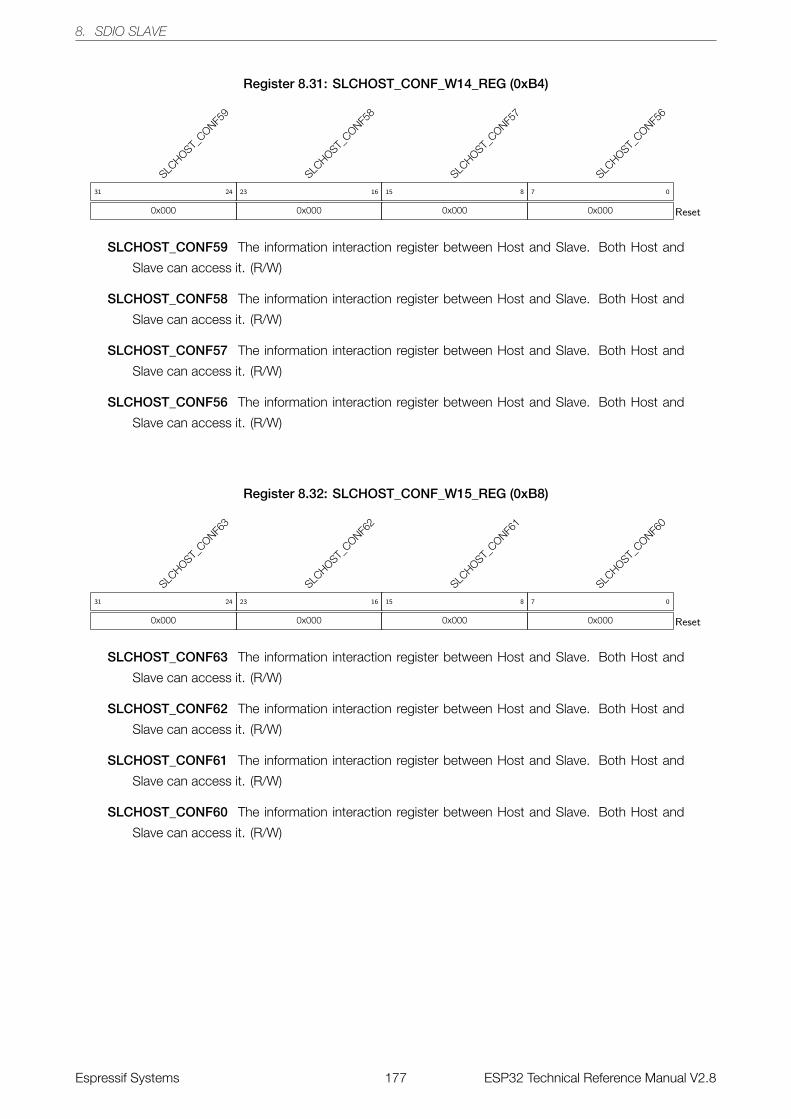
8. SDIO SLAVE
Register 8.31: SLCHOST_CONF_W14_REG (0xB4)
SLCHOST_
CONF59
0x000
31 24
SLCHOST_
CONF58
0x000
23 16
SLCHOST_
CONF57
0x000
15 8
SLCHOST_
CONF56
0x000
7 0
Reset
SLCHOST_CONF59 The information interaction register between Host and Slave. Both Host and
Slave can access it. (R/W)
SLCHOST_CONF58 The information interaction register between Host and Slave. Both Host and
Slave can access it. (R/W)
SLCHOST_CONF57 The information interaction register between Host and Slave. Both Host and
Slave can access it. (R/W)
SLCHOST_CONF56 The information interaction register between Host and Slave. Both Host and
Slave can access it. (R/W)
Register 8.32: SLCHOST_CONF_W15_REG (0xB8)
SLCHOST_
CONF63
0x000
31 24
SLCHOST_
CONF62
0x000
23 16
SLCHOST_
CONF61
0x000
15 8
SLCHOST_
CONF60
0x000
7 0
Reset
SLCHOST_CONF63 The information interaction register between Host and Slave. Both Host and
Slave can access it. (R/W)
SLCHOST_CONF62 The information interaction register between Host and Slave. Both Host and
Slave can access it. (R/W)
SLCHOST_CONF61 The information interaction register between Host and Slave. Both Host and
Slave can access it. (R/W)
SLCHOST_CONF60 The information interaction register between Host and Slave. Both Host and
Slave can access it. (R/W)
Espressif Systems 177 ESP32 Technical Reference Manual V2.8
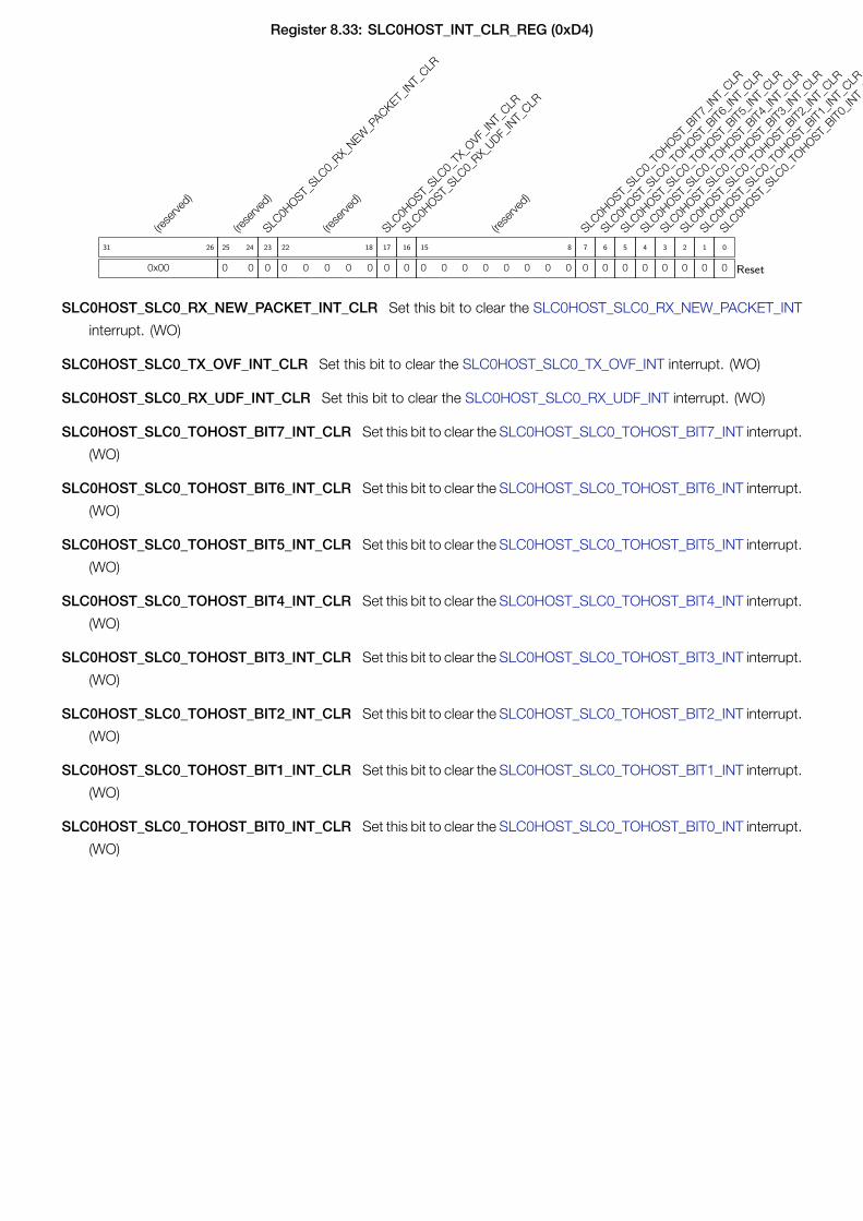
8. SDIO SLAVE
Register 8.33: SLC0HOST_INT_CLR_REG (0xD4)
(rese
rved)
0x00
31 26
(rese
rved)
0 0
25 24
SLC0H
OST_SLC
0_RX_
NEW_P
ACKET_IN
T_CLR
0
23
(rese
rved)
0 0 0 0 0
22 18
SLC0H
OST_SLC
0_TX
_OVF_
INT_
CLR
0
17
SLC0H
OST_SLC
0_RX_
UDF_IN
T_CLR
0
16
(rese
rved)
0 0 0 0 0 0 0 0
15 8
SLC0H
OST_SLC
0_TO
HOST_BIT7
_INT_
CLR
0
7
SLC0H
OST_SLC
0_TO
HOST_BIT6
_INT_
CLR
0
6
SLC0H
OST_SLC
0_TO
HOST_BIT5
_INT_
CLR
0
5
SLC0H
OST_SLC
0_TO
HOST_BIT4
_INT_
CLR
0
4
SLC0H
OST_SLC
0_TO
HOST_BIT3
_INT_
CLR
0
3
SLC0H
OST_SLC
0_TO
HOST_BIT2
_INT_
CLR
0
2
SLC0H
OST_SLC
0_TO
HOST_BIT1
_INT_
CLR
0
1
SLC0H
OST_SLC
0_TO
HOST_BIT0
_INT_
CLR
0
0
Reset
SLC0HOST_SLC0_RX_NEW_PACKET_INT_CLR Set this bit to clear the SLC0HOST_SLC0_RX_NEW_PACKET_INT
interrupt. (WO)
SLC0HOST_SLC0_TX_OVF_INT_CLR Set this bit to clear the SLC0HOST_SLC0_TX_OVF_INT interrupt. (WO)
SLC0HOST_SLC0_RX_UDF_INT_CLR Set this bit to clear the SLC0HOST_SLC0_RX_UDF_INT interrupt. (WO)
SLC0HOST_SLC0_TOHOST_BIT7_INT_CLR Set this bit to clear the SLC0HOST_SLC0_TOHOST_BIT7_INT interrupt.
(WO)
SLC0HOST_SLC0_TOHOST_BIT6_INT_CLR Set this bit to clear the SLC0HOST_SLC0_TOHOST_BIT6_INT interrupt.
(WO)
SLC0HOST_SLC0_TOHOST_BIT5_INT_CLR Set this bit to clear the SLC0HOST_SLC0_TOHOST_BIT5_INT interrupt.
(WO)
SLC0HOST_SLC0_TOHOST_BIT4_INT_CLR Set this bit to clear the SLC0HOST_SLC0_TOHOST_BIT4_INT interrupt.
(WO)
SLC0HOST_SLC0_TOHOST_BIT3_INT_CLR Set this bit to clear the SLC0HOST_SLC0_TOHOST_BIT3_INT interrupt.
(WO)
SLC0HOST_SLC0_TOHOST_BIT2_INT_CLR Set this bit to clear the SLC0HOST_SLC0_TOHOST_BIT2_INT interrupt.
(WO)
SLC0HOST_SLC0_TOHOST_BIT1_INT_CLR Set this bit to clear the SLC0HOST_SLC0_TOHOST_BIT1_INT interrupt.
(WO)
SLC0HOST_SLC0_TOHOST_BIT0_INT_CLR Set this bit to clear the SLC0HOST_SLC0_TOHOST_BIT0_INT interrupt.
(WO)
Espressif Systems 178 ESP32 Technical Reference Manual V2.8
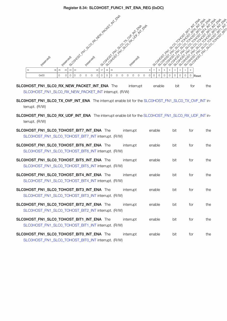
8. SDIO SLAVE
Register 8.34: SLC0HOST_FUNC1_INT_ENA_REG (0xDC)
(rese
rved)
0x00
31 26
(rese
rved)
0 0
25 24
SLC0H
OST_FN
1_SLC
0_RX_
NEW_P
ACKET_IN
T_ENA
0
23
(rese
rved)
0 0 0 0 0
22 18
SLC0H
OST_FN
1_SLC
0_TX
_OVF_
INT_
ENA
0
17
SLC0H
OST_FN
1_SLC
0_RX_
UDF_IN
T_ENA
0
16
(rese
rved)
0 0 0 0 0 0 0 0
15 8
SLC0H
OST_FN
1_SLC
0_TO
HOST_BIT7
_INT_
ENA
0
7
SLC0H
OST_FN
1_SLC
0_TO
HOST_BIT6
_INT_
ENA
0
6
SLC0H
OST_FN
1_SLC
0_TO
HOST_BIT5
_INT_
ENA
0
5
SLC0H
OST_FN
1_SLC
0_TO
HOST_BIT4
_INT_
ENA
0
4
SLC0H
OST_FN
1_SLC
0_TO
HOST_BIT3
_INT_
ENA
0
3
SLC0H
OST_FN
1_SLC
0_TO
HOST_BIT2
_INT_
ENA
0
2
SLC0H
OST_FN
1_SLC
0_TO
HOST_BIT1
_INT_
ENA
0
1
SLC0H
OST_FN
1_SLC
0_TO
HOST_BIT0
_INT_
ENA
0
0
Reset
SLC0HOST_FN1_SLC0_RX_NEW_PACKET_INT_ENA The interrupt enable bit for the
SLC0HOST_FN1_SLC0_RX_NEW_PACKET_INT interrupt. (R/W)
SLC0HOST_FN1_SLC0_TX_OVF_INT_ENA The interrupt enable bit for the SLC0HOST_FN1_SLC0_TX_OVF_INT in-
terrupt. (R/W)
SLC0HOST_FN1_SLC0_RX_UDF_INT_ENA The interrupt enable bit for the SLC0HOST_FN1_SLC0_RX_UDF_INT in-
terrupt. (R/W)
SLC0HOST_FN1_SLC0_TOHOST_BIT7_INT_ENA The interrupt enable bit for the
SLC0HOST_FN1_SLC0_TOHOST_BIT7_INT interrupt. (R/W)
SLC0HOST_FN1_SLC0_TOHOST_BIT6_INT_ENA The interrupt enable bit for the
SLC0HOST_FN1_SLC0_TOHOST_BIT6_INT interrupt. (R/W)
SLC0HOST_FN1_SLC0_TOHOST_BIT5_INT_ENA The interrupt enable bit for the
SLC0HOST_FN1_SLC0_TOHOST_BIT5_INT interrupt. (R/W)
SLC0HOST_FN1_SLC0_TOHOST_BIT4_INT_ENA The interrupt enable bit for the
SLC0HOST_FN1_SLC0_TOHOST_BIT4_INT interrupt. (R/W)
SLC0HOST_FN1_SLC0_TOHOST_BIT3_INT_ENA The interrupt enable bit for the
SLC0HOST_FN1_SLC0_TOHOST_BIT3_INT interrupt. (R/W)
SLC0HOST_FN1_SLC0_TOHOST_BIT2_INT_ENA The interrupt enable bit for the
SLC0HOST_FN1_SLC0_TOHOST_BIT2_INT interrupt. (R/W)
SLC0HOST_FN1_SLC0_TOHOST_BIT1_INT_ENA The interrupt enable bit for the
SLC0HOST_FN1_SLC0_TOHOST_BIT1_INT interrupt. (R/W)
SLC0HOST_FN1_SLC0_TOHOST_BIT0_INT_ENA The interrupt enable bit for the
SLC0HOST_FN1_SLC0_TOHOST_BIT0_INT interrupt. (R/W)
Espressif Systems 179 ESP32 Technical Reference Manual V2.8
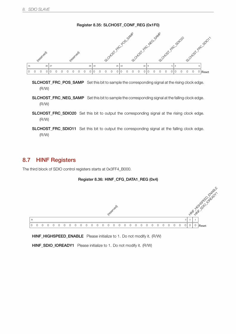
8. SDIO SLAVE
Register 8.35: SLCHOST_CONF_REG (0x1F0)
(rese
rved)
0 0 0 0
31 28
(rese
rved)
0 0 0 0 0 0 0 0
27 20
SLCHOST_
FRC_P
OS_SAM
P
0 0 0 0 0
19 15
SLCHOST_
FRC_N
EG_SAM
P
0 0 0 0 0
14 10
SLCHOST_
FRC_S
DIO20
0 0 0 0 0
9 5
SLCHOST_
FRC_S
DIO11
0 0 0 0 0
4 0
Reset
SLCHOST_FRC_POS_SAMP Set this bit to sample the corresponding signal at the rising clock edge.
(R/W)
SLCHOST_FRC_NEG_SAMP Set this bit to sample the corresponding signal at the falling clock edge.
(R/W)
SLCHOST_FRC_SDIO20 Set this bit to output the corresponding signal at the rising clock edge.
(R/W)
SLCHOST_FRC_SDIO11 Set this bit to output the corresponding signal at the falling clock edge.
(R/W)
8.7 HINF Registers
The third block of SDIO control registers starts at 0x3FF4_B000.
Register 8.36: HINF_CFG_DATA1_REG (0x4)
(rese
rved)
0 0 0 0 0 0 0 0 0 0 0 0 0 0 0 0 0 0 0 0 0 0 0 0 0 0 0 0 0
31 3
HINF_
HIGHSPEED_E
NABLE
0
2
HINF_
SDIO_IO
READY1
0
1
Reset
HINF_HIGHSPEED_ENABLE Please initialize to 1. Do not modify it. (R/W)
HINF_SDIO_IOREADY1 Please initialize to 1. Do not modify it. (R/W)
Espressif Systems 180 ESP32 Technical Reference Manual V2.8
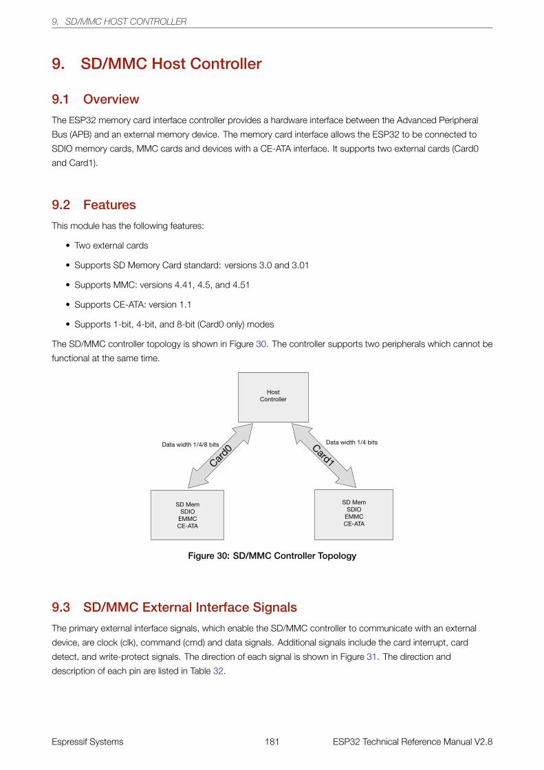
9. SD/MMC HOST CONTROLLER
9. SD/MMC Host Controller
9.1 Overview
The ESP32 memory card interface controller provides a hardware interface between the Advanced Peripheral
Bus (APB) and an external memory device. The memory card interface allows the ESP32 to be connected to
SDIO memory cards, MMC cards and devices with a CE-ATA interface. It supports two external cards (Card0
and Card1).
9.2 Features
This module has the following features:
• Two external cards
• Supports SD Memory Card standard: versions 3.0 and 3.01
• Supports MMC: versions 4.41, 4.5, and 4.51
• Supports CE-ATA: version 1.1
• Supports 1-bit, 4-bit, and 8-bit (Card0 only) modes
The SD/MMC controller topology is shown in Figure 30. The controller supports two peripherals which cannot be
functional at the same time.
Figure 30: SD/MMC Controller Topology
9.3 SD/MMC External Interface Signals
The primary external interface signals, which enable the SD/MMC controller to communicate with an external
device, are clock (clk), command (cmd) and data signals. Additional signals include the card interrupt, card
detect, and write-protect signals. The direction of each signal is shown in Figure 31. The direction and
description of each pin are listed in Table 32.
Espressif Systems 181 ESP32 Technical Reference Manual V2.8
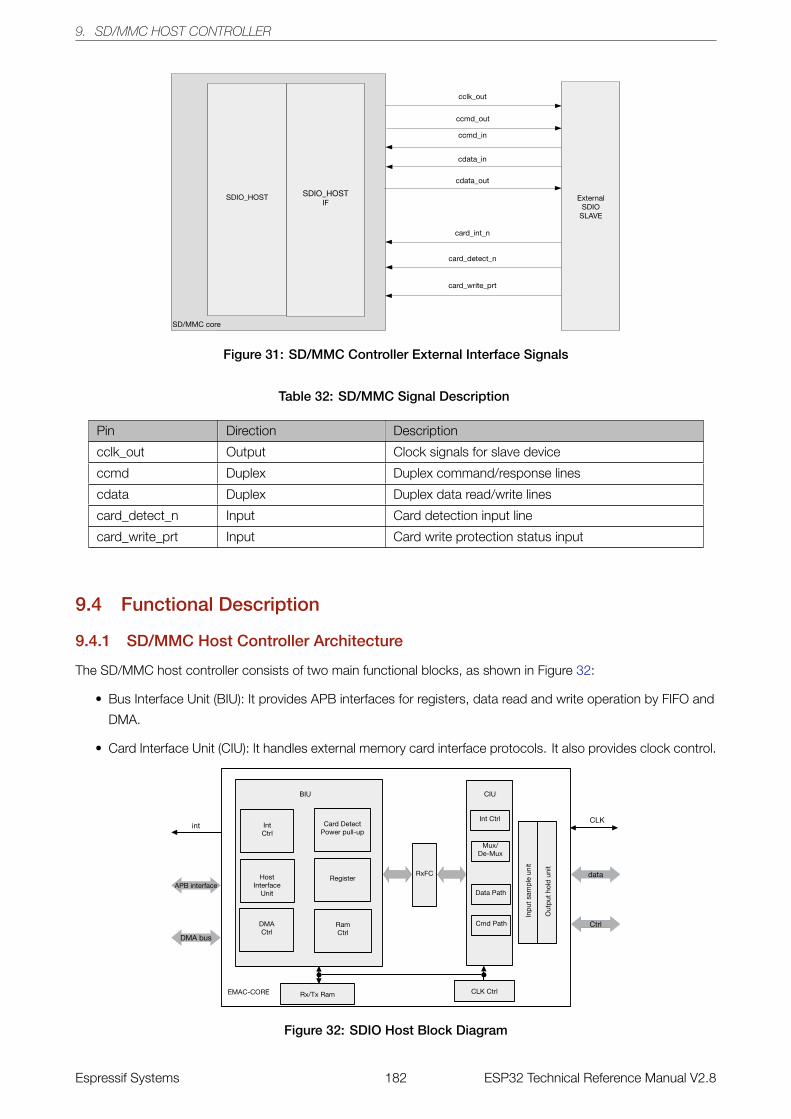
9. SD/MMC HOST CONTROLLER
Figure 31: SD/MMC Controller External Interface Signals
Table 32: SD/MMC Signal Description
Pin Direction Description
cclk_out Output Clock signals for slave device
ccmd Duplex Duplex command/response lines
cdata Duplex Duplex data read/write lines
card_detect_n Input Card detection input line
card_write_prt Input Card write protection status input
9.4 Functional Description
9.4.1 SD/MMC Host Controller Architecture
The SD/MMC host controller consists of two main functional blocks, as shown in Figure 32:
• Bus Interface Unit (BIU): It provides APB interfaces for registers, data read and write operation by FIFO and
DMA.
• Card Interface Unit (CIU): It handles external memory card interface protocols. It also provides clock control.
Figure 32: SDIO Host Block Diagram
Espressif Systems 182 ESP32 Technical Reference Manual V2.8
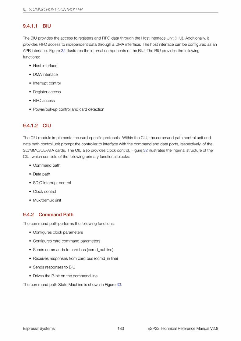
9. SD/MMC HOST CONTROLLER
9.4.1.1 BIU
The BIU provides the access to registers and FIFO data through the Host Interface Unit (HIU). Additionally, it
provides FIFO access to independent data through a DMA interface. The host interface can be configured as an
APB interface. Figure 32 illustrates the internal components of the BIU. The BIU provides the following
functions:
• Host interface
• DMA interface
• Interrupt control
• Register access
• FIFO access
• Power/pull-up control and card detection
9.4.1.2 CIU
The CIU module implements the card-specific protocols. Within the CIU, the command path control unit and
data path control unit prompt the controller to interface with the command and data ports, respectively, of the
SD/MMC/CE-ATA cards. The CIU also provides clock control. Figure 32 illustrates the internal structure of the
CIU, which consists of the following primary functional blocks:
• Command path
• Data path
• SDIO interrupt control
• Clock control
• Mux/demux unit
9.4.2 Command Path
The command path performs the following functions:
• Configures clock parameters
• Configures card command parameters
• Sends commands to card bus (ccmd_out line)
• Receives responses from card bus (ccmd_in line)
• Sends responses to BIU
• Drives the P-bit on the command line
The command path State Machine is shown in Figure 33.
Espressif Systems 183 ESP32 Technical Reference Manual V2.8
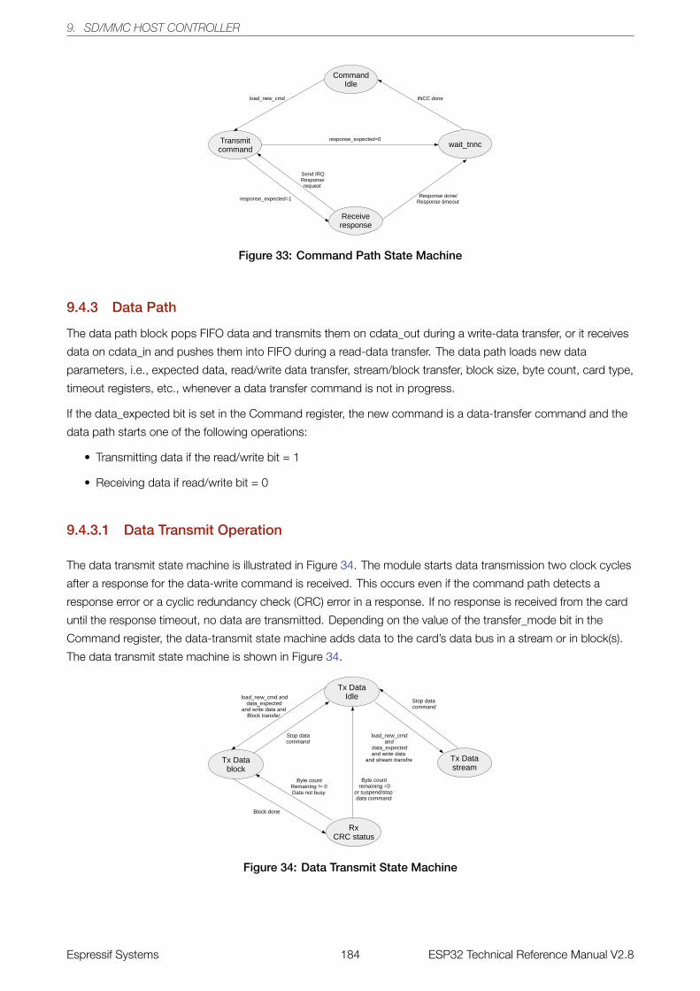
9. SD/MMC HOST CONTROLLER
Figure 33: Command Path State Machine
9.4.3 Data Path
The data path block pops FIFO data and transmits them on cdata_out during a write-data transfer, or it receives
data on cdata_in and pushes them into FIFO during a read-data transfer. The data path loads new data
parameters, i.e., expected data, read/write data transfer, stream/block transfer, block size, byte count, card type,
timeout registers, etc., whenever a data transfer command is not in progress.
If the data_expected bit is set in the Command register, the new command is a data-transfer command and the
data path starts one of the following operations:
• Transmitting data if the read/write bit = 1
• Receiving data if read/write bit = 0
9.4.3.1 Data Transmit Operation
The data transmit state machine is illustrated in Figure 34. The module starts data transmission two clock cycles
after a response for the data-write command is received. This occurs even if the command path detects a
response error or a cyclic redundancy check (CRC) error in a response. If no response is received from the card
until the response timeout, no data are transmitted. Depending on the value of the transfer_mode bit in the
Command register, the data-transmit state machine adds data to the card’s data bus in a stream or in block(s).
The data transmit state machine is shown in Figure 34.
Figure 34: Data Transmit State Machine
Espressif Systems 184 ESP32 Technical Reference Manual V2.8
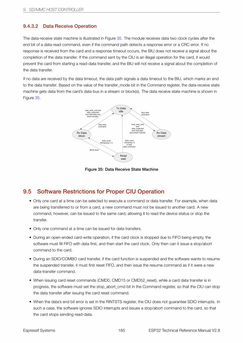
9. SD/MMC HOST CONTROLLER
9.4.3.2 Data Receive Operation
The data-receive state machine is illustrated in Figure 35. The module receives data two clock cycles after the
end bit of a data-read command, even if the command path detects a response error or a CRC error. If no
response is received from the card and a response timeout occurs, the BIU does not receive a signal about the
completion of the data transfer. If the command sent by the CIU is an illegal operation for the card, it would
prevent the card from starting a read-data transfer, and the BIU will not receive a signal about the completion of
the data transfer.
If no data are received by the data timeout, the data path signals a data timeout to the BIU, which marks an end
to the data transfer. Based on the value of the transfer_mode bit in the Command register, the data-receive state
machine gets data from the card’s data bus in a stream or block(s). The data receive state machine is shown in
Figure 35.
Figure 35: Data Receive State Machine
9.5 Software Restrictions for Proper CIU Operation
• Only one card at a time can be selected to execute a command or data transfer. For example, when data
are being transferred to or from a card, a new command must not be issued to another card. A new
command, however, can be issued to the same card, allowing it to read the device status or stop the
transfer.
• Only one command at a time can be issued for data transfers.
• During an open-ended card-write operation, if the card clock is stopped due to FIFO being empty, the
software must fill FIFO with data first, and then start the card clock. Only then can it issue a stop/abort
command to the card.
• During an SDIO/COMBO card transfer, if the card function is suspended and the software wants to resume
the suspended transfer, it must first reset FIFO, and then issue the resume command as if it were a new
data-transfer command.
• When issuing card reset commands (CMD0, CMD15 or CMD52_reset), while a card data transfer is in
progress, the software must set the stop_abort_cmd bit in the Command register, so that the CIU can stop
the data transfer after issuing the card reset command.
• When the data’s end bit error is set in the RINTSTS register, the CIU does not guarantee SDIO interrupts. In
such a case, the software ignores SDIO interrupts and issues a stop/abort command to the card, so that
the card stops sending read-data.
Espressif Systems 185 ESP32 Technical Reference Manual V2.8
9. SD/MMC HOST CONTROLLER
• If the card clock is stopped due to FIFO being full during a card read, the software will read at least two
FIFO locations to restart the card clock.
• Only one CE-ATA device at a time can be selected for a command or data transfer. For example, when
data are transferred from a CE-ATA device, a new command should not be sent to another CE-ATA device.
• If a CE-ATA device’s interrupts are enabled (nIEN=0), a new RW_BLK command should not be sent to the
same device if the execution of a RW_BLK command is already in progress (the RW_BLK command used
in this databook is the RW_MULTIPLE_BLOCK MMC command defined by the CE-ATA specifications).
Only the CCSD can be sent while waiting for the CCS.
• If, however, a CE-ATA device’s interrupts are disabled (nIEN=1), a new command can be issued to the
same device, allowing it to read status information.
• Open-ended transfers are not supported in CE-ATA devices.
• The send_auto_stop signal is not supported (software should not set the send_auto_stop bit) in CE-ATA
transfers.
After configuring the command start bit to 1, the values of the following registers cannot be changed before a
command has been issued:
• CMD - command
• CMDARG - command argument
• BYTCNT - byte count
• BLKSIZ - block size
• CLKDIV - clock divider
• CKLENA - clock enable
• CLKSRC - clock source
• TMOUT - timeout
• CTYPE - card type
9.6 RAM for Receiving and Sending Data
The submodule RAM is a buffer area for sending and receiving data. It can be divided into two units: the one is for
sending data, and the other is for receiving data. The process of sending and receiving data can also be achieved
by the CPU and DMA for reading and writing. The latter method is described in detail in Section 9.8.
9.6.1 Transmit RAM Module
There are two ways to enable a write operation: DMA and CPU read/write.
If SDIO-sending is enabled, data can be written to the transferred RAM module by APB interface or DMA. Data
will be written from register EMAC_FIFO to the CPU, directly, by an APB interface.
Espressif Systems 186 ESP32 Technical Reference Manual V2.8
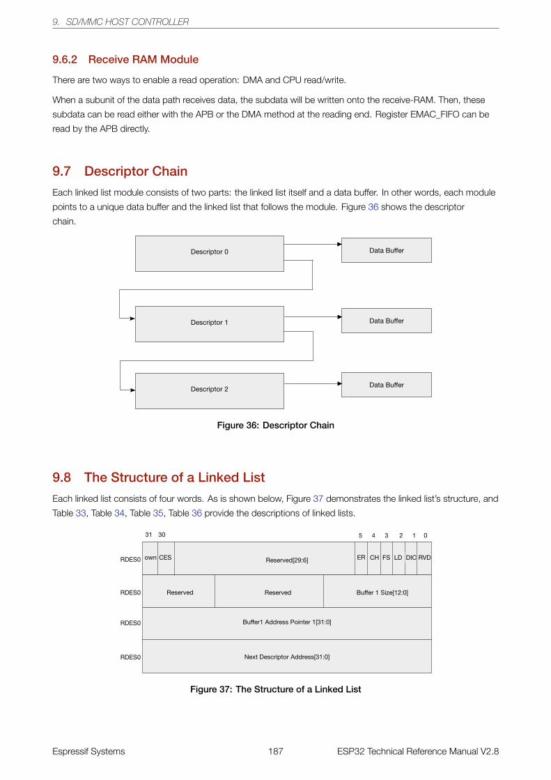
9. SD/MMC HOST CONTROLLER
9.6.2 Receive RAM Module
There are two ways to enable a read operation: DMA and CPU read/write.
When a subunit of the data path receives data, the subdata will be written onto the receive-RAM. Then, these
subdata can be read either with the APB or the DMA method at the reading end. Register EMAC_FIFO can be
read by the APB directly.
9.7 Descriptor Chain
Each linked list module consists of two parts: the linked list itself and a data buffer. In other words, each module
points to a unique data buffer and the linked list that follows the module. Figure 36 shows the descriptor
chain.
Figure 36: Descriptor Chain
9.8 The Structure of a Linked List
Each linked list consists of four words. As is shown below, Figure 37 demonstrates the linked list’s structure, and
Table 33, Table 34, Table 35, Table 36 provide the descriptions of linked lists.
Figure 37: The Structure of a Linked List
Espressif Systems 187 ESP32 Technical Reference Manual V2.8
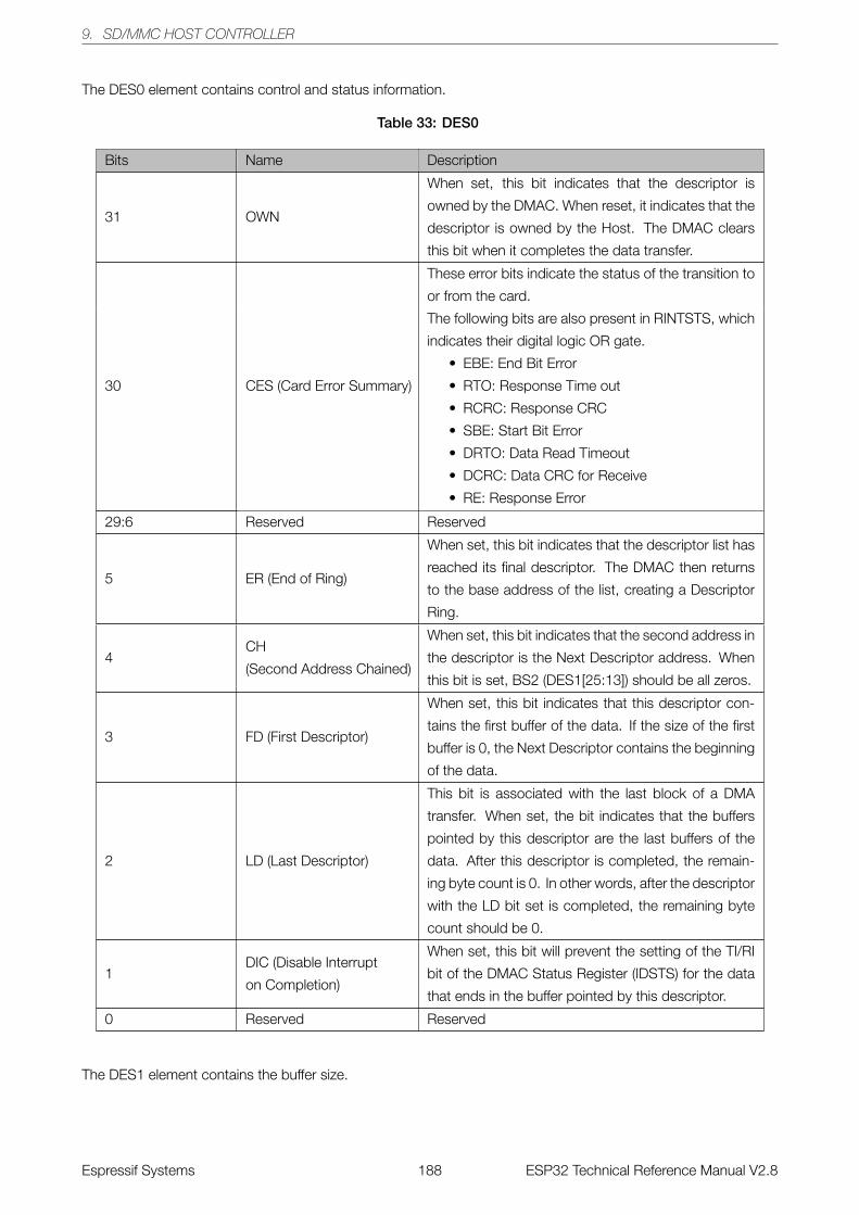
9. SD/MMC HOST CONTROLLER
The DES0 element contains control and status information.
Table 33: DES0
Bits Name Description
31 OWN
When set, this bit indicates that the descriptor is
owned by the DMAC. When reset, it indicates that the
descriptor is owned by the Host. The DMAC clears
this bit when it completes the data transfer.
30 CES (Card Error Summary)
These error bits indicate the status of the transition to
or from the card.
The following bits are also present in RINTSTS, which
indicates their digital logic OR gate.
• EBE: End Bit Error
• RTO: Response Time out
• RCRC: Response CRC
• SBE: Start Bit Error
• DRTO: Data Read Timeout
• DCRC: Data CRC for Receive
• RE: Response Error
29:6 Reserved Reserved
5 ER (End of Ring)
When set, this bit indicates that the descriptor list has
reached its final descriptor. The DMAC then returns
to the base address of the list, creating a Descriptor
Ring.
4CH
(Second Address Chained)
When set, this bit indicates that the second address in
the descriptor is the Next Descriptor address. When
this bit is set, BS2 (DES1[25:13]) should be all zeros.
3 FD (First Descriptor)
When set, this bit indicates that this descriptor con-
tains the first buffer of the data. If the size of the first
buffer is 0, the Next Descriptor contains the beginning
of the data.
2 LD (Last Descriptor)
This bit is associated with the last block of a DMA
transfer. When set, the bit indicates that the buffers
pointed by this descriptor are the last buffers of the
data. After this descriptor is completed, the remain-
ing byte count is 0. In other words, after the descriptor
with the LD bit set is completed, the remaining byte
count should be 0.
1DIC (Disable Interrupt
on Completion)
When set, this bit will prevent the setting of the TI/RI
bit of the DMAC Status Register (IDSTS) for the data
that ends in the buffer pointed by this descriptor.
0 Reserved Reserved
The DES1 element contains the buffer size.
Espressif Systems 188 ESP32 Technical Reference Manual V2.8
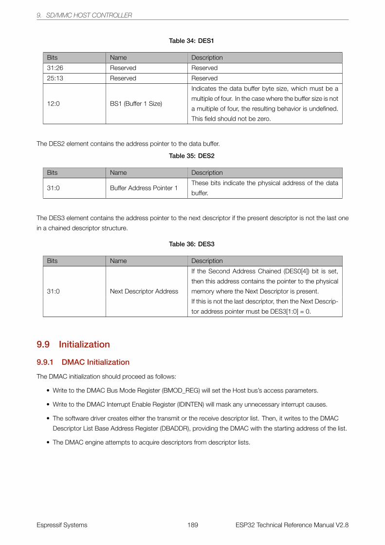
9. SD/MMC HOST CONTROLLER
Table 34: DES1
Bits Name Description
31:26 Reserved Reserved
25:13 Reserved Reserved
12:0 BS1 (Buffer 1 Size)
Indicates the data buffer byte size, which must be a
multiple of four. In the case where the buffer size is not
a multiple of four, the resulting behavior is undefined.
This field should not be zero.
The DES2 element contains the address pointer to the data buffer.
Table 35: DES2
Bits Name Description
31:0 Buffer Address Pointer 1These bits indicate the physical address of the data
buffer.
The DES3 element contains the address pointer to the next descriptor if the present descriptor is not the last one
in a chained descriptor structure.
Table 36: DES3
Bits Name Description
31:0 Next Descriptor Address
If the Second Address Chained (DES0[4]) bit is set,
then this address contains the pointer to the physical
memory where the Next Descriptor is present.
If this is not the last descriptor, then the Next Descrip-
tor address pointer must be DES3[1:0] = 0.
9.9 Initialization
9.9.1 DMAC Initialization
The DMAC initialization should proceed as follows:
• Write to the DMAC Bus Mode Register (BMOD_REG) will set the Host bus’s access parameters.
• Write to the DMAC Interrupt Enable Register (IDINTEN) will mask any unnecessary interrupt causes.
• The software driver creates either the transmit or the receive descriptor list. Then, it writes to the DMAC
Descriptor List Base Address Register (DBADDR), providing the DMAC with the starting address of the list.
• The DMAC engine attempts to acquire descriptors from descriptor lists.
Espressif Systems 189 ESP32 Technical Reference Manual V2.8
9. SD/MMC HOST CONTROLLER
9.9.2 DMAC Transmission Initialization
The DMAC transmission occurs as follows:
1. The Host sets up the elements (DES0-DES3) for transmission, and sets the OWN bit (DES0[31]). The Host
also prepares the data buffer.
2. The Host programs the write-data command in the CMD register in BIU.
3. The Host also programs the required transmit threshold (TX_WMARK field in FIFOTH register).
4. The DMAC engine fetches the descriptor and checks the OWN bit. If the OWN bit is not set, it means that
the host owns the descriptor. In this case, the DMAC enters a suspend-state and asserts the Descriptor
Unable interrupt in the IDSTS register. In such a case, the host needs to release the DMAC by writing any
value to PLDMND_REG.
5. It then waits for the Command Done (CD) bit and no errors from BIU, which indicates that a transfer can be
done.
6. Subsequently, the DMAC engine waits for a DMA interface request (dw_dma_req) from BIU. This request
will be generated, based on the programmed transmit-threshold value. For the last bytes of data which
cannot be accessed using a burst, single transfers are performed on the AHB Master Interface.
7. The DMAC fetches the transmit data from the data buffer in the Host memory and transfers them to FIFO
for transmission to card.
8. When data span across multiple descriptors, the DMAC fetches the next descriptor and extends its
operation using the following descriptor. The last descriptor bit indicates whether the data span multiple
descriptors or not.
9. When data transmission is complete, the status information is updated in the IDSTS register by setting the
Transmit Interrupt, if it has already been enabled. Also, the OWN bit is cleared by the DMAC by performing
a write transaction to DES0.
9.9.3 DMAC Reception Initialization
The DMAC reception occurs as follows:
1. The Host sets up the element (DES0-DES3) for reception, and sets the OWN bit (DES0[31]).
2. The Host programs the read-data command in the CMD register in BIU.
3. Then, the Host programs the required level of the receive-threshold (RX_WMARK field in FIFOTH register).
4. The DMAC engine fetches the descriptor and checks the OWN bit. If the OWN bit is not set, it means that
the host owns the descriptor. In this case, the DMA enters a suspend-state and asserts the Descriptor
Unable interrupt in the IDSTS register. In such a case, the host needs to release the DMAC by writing any
value to PLDMND_REG.
5. It then waits for the Command Done (CD) bit and no errors from BIU, which indicates that a transfer can be
done.
6. The DMAC engine then waits for a DMA interface request (dw_dma_req) from BIU. This request will be
generated, based on the programmed receive-threshold value. For the last bytes of the data which cannot
be accessed using a burst, single transfers are performed on the AHB.
7. The DMAC fetches the data from FIFO and transfers them to the Host memory.
Espressif Systems 190 ESP32 Technical Reference Manual V2.8
9. SD/MMC HOST CONTROLLER
8. When data span across multiple descriptors, the DMAC will fetch the next descriptor and extend its
operation using the following descriptor. The last descriptor bit indicates whether the data span multiple
descriptors or not.
9. When data reception is complete, the status information is updated in the IDSTS register by setting
Receive-Interrupt, if it has already been enabled. Also, the OWN bit is cleared by the DMAC by performing
a write-transaction to DES0.
9.10 Clock Phase Selection
If the setup time requirements for the input or output data signal are not met, users can specify the clock phase,
as shown in the figure below.
Figure 38: Clock Phase Selection
Please find detailed information on the clock phase selection register CLK_EDGE_SEL in Section
Registers.
9.11 Interrupt
Interrupts can be generated as a result of various events. The IDSTS register contains all the bits that might
cause an interrupt. The IDINTEN register contains an enable bit for each of the events that can cause an
interrupt.
There are two groups of summary interrupts, ”Normal” ones (bit8 NIS) and ”Abnormal” ones (bit9 AIS), as
outlined in the IDSTS register. Interrupts are cleared by writing 1 to the position of the corresponding bit. When all
the enabled interrupts within a group are cleared, the corresponding summary bit is also cleared. When both
summary bits are cleared, the interrupt signal dmac_intr_o is de-asserted (stops signalling).
Espressif Systems 191 ESP32 Technical Reference Manual V2.8
9. SD/MMC HOST CONTROLLER
Interrupts are not queued up, and if a new interrupt-event occurs before the driver has responded to it, no
additional interrupts are generated. For example, the Receive Interrupt IDSTS[1] indicates that one or more data
were transferred to the Host buffer.
An interrupt is generated only once for concurrent events. The driver must scan the IDSTS register for the
interrupt cause.
9.12 Register Summary
Name Description Address Access
CTRL_REG Control register 0x0000 R/W
CLKDIV_REG Clock divider configuration register 0x0008 R/W
CLKSRC_REG Clock source selection register 0x000C R/W
CLKENA_REG Clock enable register 0x0010 R/W
TMOUT_REG Data and response timeout configuration register 0x0014 R/W
CTYPE_REG Card bus width configuration register 0x0018 R/W
BLKSIZ_REG Card data block size configuration register 0x001C R/W
BYTCNT_REG Data transfer length configuration register 0x0020 R/W
INTMASK_REG SDIO interrupt mask register 0x0024 R/W
CMDARG_REG Command argument data register 0x0028 R/W
CMD_REG Command and boot configuration register 0x002C R/W
RESP0_REG Response data register 0x0030 RO
RESP1_REG Long response data register 0x0034 RO
RESP2_REG Long response data register 0x0038 RO
RESP3_REG Long response data register 0x003C RO
MINTSTS_REG Masked interrupt status register 0x0040 RO
RINTSTS_REG Raw interrupt status register 0x0044 R/W
STATUS_REG SD/MMC status register 0x0048 RO
FIFOTH_REG FIFO configuration register 0x004C R/W
CDETECT_REG Card detect register 0x0050 RO
WRTPRT_REG Card write protection (WP) status register 0x0054 RO
TCBCNT_REG Transferred byte count register 0x005C RO
TBBCNT_REG Transferred byte count register 0x0060 RO
DEBNCE_REG Debounce filter time configuration register 0x0064 R/W
USRID_REG User ID (scratchpad) register 0x0068 R/W
RST_N_REG Card reset register 0x0078 R/W
BMOD_REG Burst mode transfer configuration register 0x0080 R/W
PLDMND_REG Poll demand configuration register 0x0084 WO
DBADDR_REG Descriptor base address register 0x0088 R/W
IDSTS_REG IDMAC status register 0x008C R/W
IDINTEN_REG IDMAC interrupt enable register 0x0090 R/W
DSCADDR_REG Host descriptor address pointer 0x0094 RO
BUFADDR_REG Host buffer address pointer register 0x0098 RO
CLK_EDGE_SEL Clock phase selection register 0x0800 R/W
Espressif Systems 192 ESP32 Technical Reference Manual V2.8
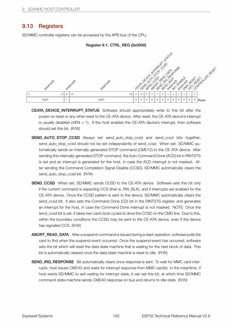
9. SD/MMC HOST CONTROLLER
9.13 Registers
SD/MMC controller registers can be accessed by the APB bus of the CPU.
Register 9.1: CTRL_REG (0x0000)
(rese
rved)
0x00
31 25
(rese
rved)
1
24
(rese
rved)
0x00
131 120
CEATA_D
EVICE_IN
TERRUPT_
STATU
S
0
11
SEND_AUTO
_STO
P_CCSD
0
10
SEND_CCSD
0
9
ABORT_READ_D
ATA
0
8
SEND_IRQ_R
ESPONSE
0
7
READ_WAIT
0
6
(rese
rved)
0
5
INT_
ENABLE
0
4
(rese
rved)
0
3
DMA_R
ESET
0
2
FIFO_R
ESET
0
1
CONTROLL
ER_RESET
0
0
Reset
CEATA_DEVICE_INTERRUPT_STATUS Software should appropriately write to this bit after the
power-on reset or any other reset to the CE-ATA device. After reset, the CE-ATA device’s interrupt
is usually disabled (nIEN = 1). If the host enables the CE-ATA device’s interrupt, then software
should set this bit. (R/W)
SEND_AUTO_STOP_CCSD Always set send_auto_stop_ccsd and send_ccsd bits together;
send_auto_stop_ccsd should not be set independently of send_ccsd. When set, SD/MMC au-
tomatically sends an internally-generated STOP command (CMD12) to the CE-ATA device. After
sending this internally-generated STOP command, the Auto Command Done (ACD) bit in RINTSTS
is set and an interrupt is generated for the host, in case the ACD interrupt is not masked. Af-
ter sending the Command Completion Signal Disable (CCSD), SD/MMC automatically clears the
send_auto_stop_ccsd bit. (R/W)
SEND_CCSD When set, SD/MMC sends CCSD to the CE-ATA device. Software sets this bit only
if the current command is expecting CCS (that is, RW_BLK), and if interrupts are enabled for the
CE-ATA device. Once the CCSD pattern is sent to the device, SD/MMC automatically clears the
send_ccsd bit. It also sets the Command Done (CD) bit in the RINTSTS register, and generates
an interrupt for the host, in case the Command Done interrupt is not masked. NOTE: Once the
send_ccsd bit is set, it takes two card clock cycles to drive the CCSD on the CMD line. Due to this,
within the boundary conditions the CCSD may be sent to the CE-ATA device, even if the device
has signalled CCS. (R/W)
ABORT_READ_DATA After a suspend-command is issued during a read-operation, software polls the
card to find when the suspend-event occurred. Once the suspend-event has occurred, software
sets the bit which will reset the data state machine that is waiting for the next block of data. This
bit is automatically cleared once the data state machine is reset to idle. (R/W)
SEND_IRQ_RESPONSE Bit automatically clears once response is sent. To wait for MMC card inter-
rupts, host issues CMD40 and waits for interrupt response from MMC card(s). In the meantime, if
host wants SD/MMC to exit waiting for interrupt state, it can set this bit, at which time SD/MMC
command state-machine sends CMD40 response on bus and returns to idle state. (R/W)
Espressif Systems 193 ESP32 Technical Reference Manual V2.8
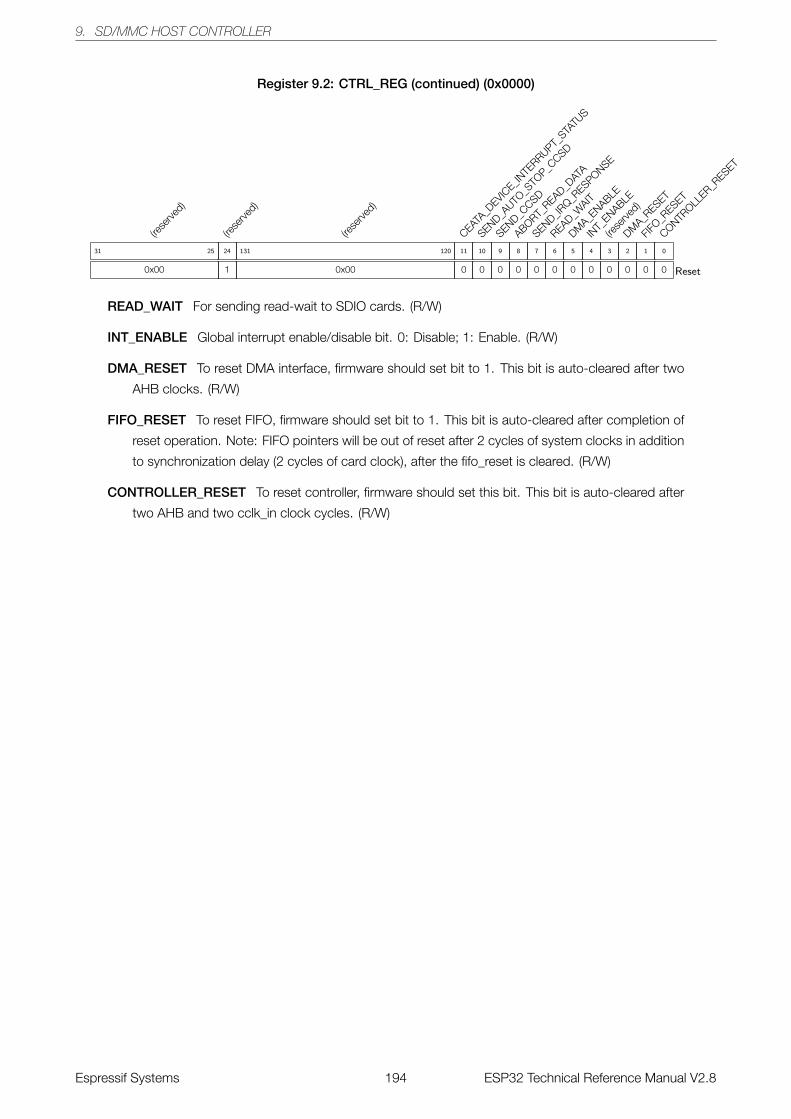
9. SD/MMC HOST CONTROLLER
Register 9.2: CTRL_REG (continued) (0x0000)
(rese
rved)
0x00
31 25
(rese
rved)
1
24
(rese
rved)
0x00
131 120
CEATA_D
EVICE_IN
TERRUPT_
STATU
S
0
11
SEND_AUTO
_STO
P_CCSD
0
10
SEND_CCSD
0
9
ABORT_READ_D
ATA
0
8
SEND_IRQ_R
ESPONSE
0
7
READ_WAIT
0
6
DMA_E
NABLE
0
5
INT_
ENABLE
0
4
(rese
rved)
0
3
DMA_R
ESET
0
2
FIFO_R
ESET
0
1
CONTROLL
ER_RESET
0
0
Reset
READ_WAIT For sending read-wait to SDIO cards. (R/W)
INT_ENABLE Global interrupt enable/disable bit. 0: Disable; 1: Enable. (R/W)
DMA_RESET To reset DMA interface, firmware should set bit to 1. This bit is auto-cleared after two
AHB clocks. (R/W)
FIFO_RESET To reset FIFO, firmware should set bit to 1. This bit is auto-cleared after completion of
reset operation. Note: FIFO pointers will be out of reset after 2 cycles of system clocks in addition
to synchronization delay (2 cycles of card clock), after the fifo_reset is cleared. (R/W)
CONTROLLER_RESET To reset controller, firmware should set this bit. This bit is auto-cleared after
two AHB and two cclk_in clock cycles. (R/W)
Espressif Systems 194 ESP32 Technical Reference Manual V2.8
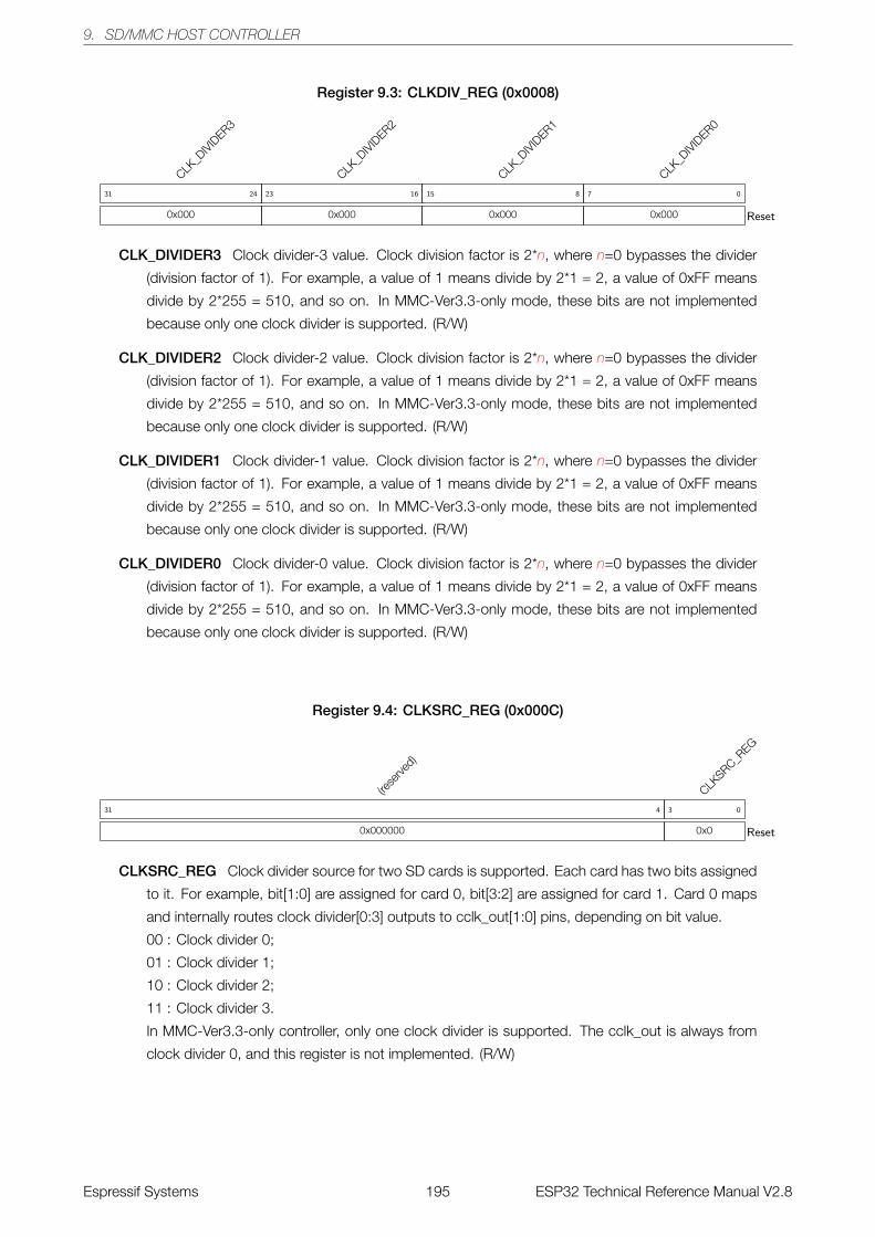
9. SD/MMC HOST CONTROLLER
Register 9.3: CLKDIV_REG (0x0008)
CLK_D
IVIDER3
0x000
31 24
CLK_D
IVIDER2
0x000
23 16
CLK_D
IVIDER1
0x000
15 8
CLK_D
IVIDER0
0x000
7 0
Reset
CLK_DIVIDER3 Clock divider-3 value. Clock division factor is 2*n, where n=0 bypasses the divider
(division factor of 1). For example, a value of 1 means divide by 2*1 = 2, a value of 0xFF means
divide by 2*255 = 510, and so on. In MMC-Ver3.3-only mode, these bits are not implemented
because only one clock divider is supported. (R/W)
CLK_DIVIDER2 Clock divider-2 value. Clock division factor is 2*n, where n=0 bypasses the divider
(division factor of 1). For example, a value of 1 means divide by 2*1 = 2, a value of 0xFF means
divide by 2*255 = 510, and so on. In MMC-Ver3.3-only mode, these bits are not implemented
because only one clock divider is supported. (R/W)
CLK_DIVIDER1 Clock divider-1 value. Clock division factor is 2*n, where n=0 bypasses the divider
(division factor of 1). For example, a value of 1 means divide by 2*1 = 2, a value of 0xFF means
divide by 2*255 = 510, and so on. In MMC-Ver3.3-only mode, these bits are not implemented
because only one clock divider is supported. (R/W)
CLK_DIVIDER0 Clock divider-0 value. Clock division factor is 2*n, where n=0 bypasses the divider
(division factor of 1). For example, a value of 1 means divide by 2*1 = 2, a value of 0xFF means
divide by 2*255 = 510, and so on. In MMC-Ver3.3-only mode, these bits are not implemented
because only one clock divider is supported. (R/W)
Register 9.4: CLKSRC_REG (0x000C)
(rese
rved)
0x000000
31 4
CLKSRC_R
EG
0x0
3 0
Reset
CLKSRC_REG Clock divider source for two SD cards is supported. Each card has two bits assigned
to it. For example, bit[1:0] are assigned for card 0, bit[3:2] are assigned for card 1. Card 0 maps
and internally routes clock divider[0:3] outputs to cclk_out[1:0] pins, depending on bit value.
00 : Clock divider 0;
01 : Clock divider 1;
10 : Clock divider 2;
11 : Clock divider 3.
In MMC-Ver3.3-only controller, only one clock divider is supported. The cclk_out is always from
clock divider 0, and this register is not implemented. (R/W)
Espressif Systems 195 ESP32 Technical Reference Manual V2.8
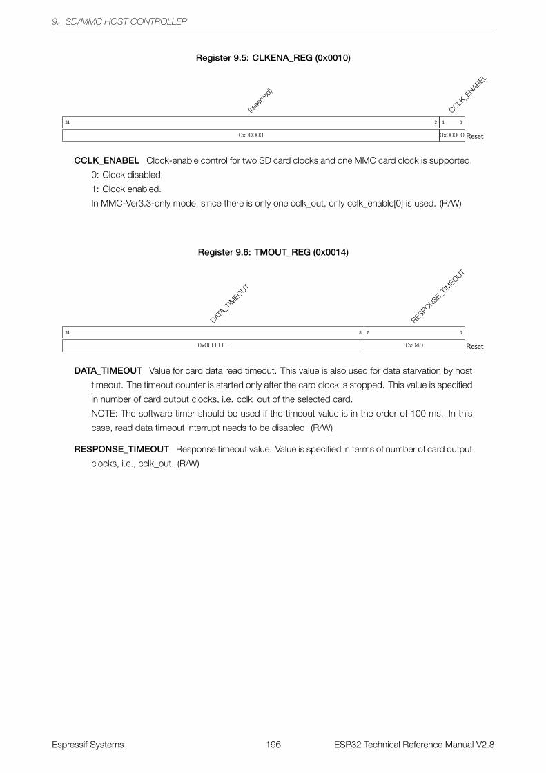
9. SD/MMC HOST CONTROLLER
Register 9.5: CLKENA_REG (0x0010)
(rese
rved)
0x00000
31 2
CCLK_E
NABEL
0x00000
1 0
Reset
CCLK_ENABEL Clock-enable control for two SD card clocks and one MMC card clock is supported.
0: Clock disabled;
1: Clock enabled.
In MMC-Ver3.3-only mode, since there is only one cclk_out, only cclk_enable[0] is used. (R/W)
Register 9.6: TMOUT_REG (0x0014)
DATA_T
IMEOUT
0x0FFFFFF
31 8
RESPONSE_TIM
EOUT
0x040
7 0
Reset
DATA_TIMEOUT Value for card data read timeout. This value is also used for data starvation by host
timeout. The timeout counter is started only after the card clock is stopped. This value is specified
in number of card output clocks, i.e. cclk_out of the selected card.
NOTE: The software timer should be used if the timeout value is in the order of 100 ms. In this
case, read data timeout interrupt needs to be disabled. (R/W)
RESPONSE_TIMEOUT Response timeout value. Value is specified in terms of number of card output
clocks, i.e., cclk_out. (R/W)
Espressif Systems 196 ESP32 Technical Reference Manual V2.8
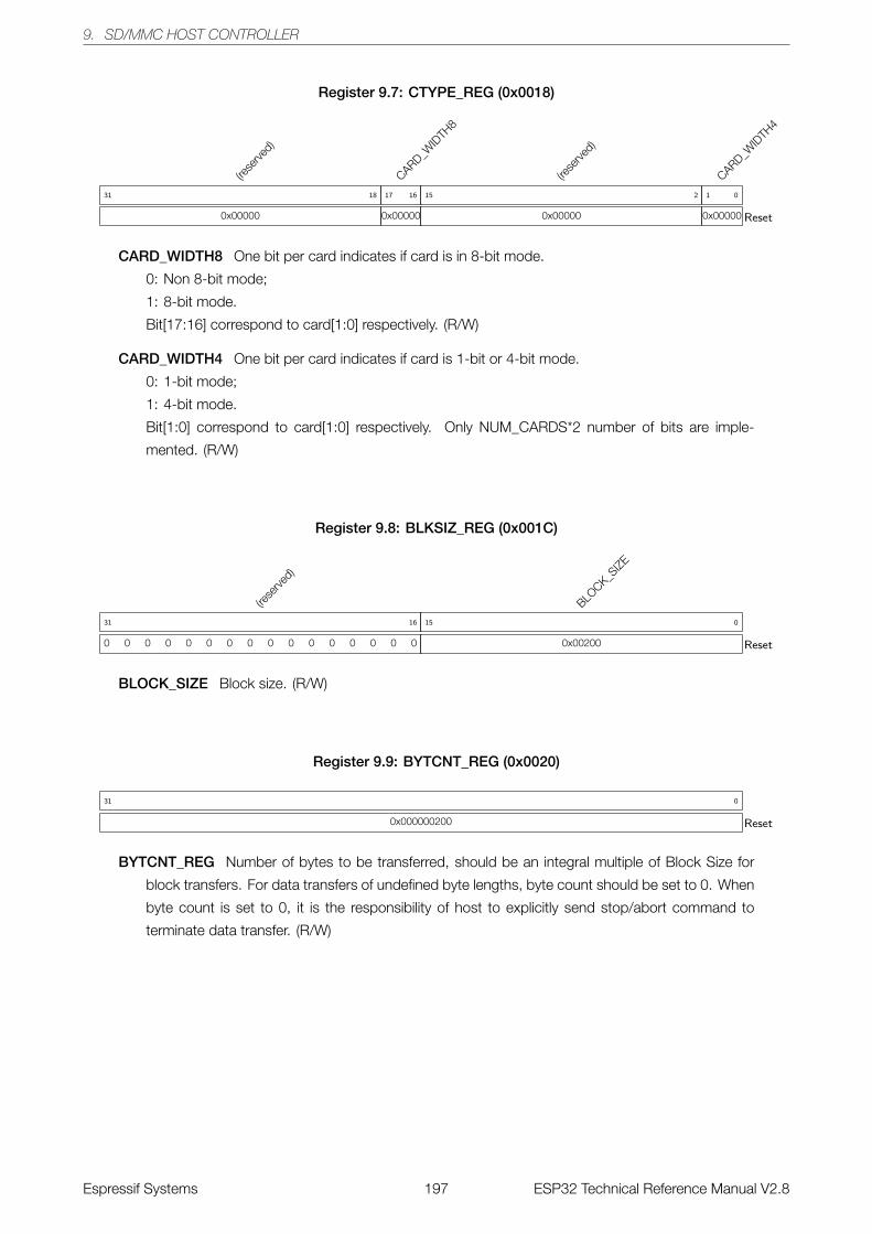
9. SD/MMC HOST CONTROLLER
Register 9.7: CTYPE_REG (0x0018)
(rese
rved)
0x00000
31 18
CARD_WID
TH8
0x00000
17 16
(rese
rved)
0x00000
15 2
CARD_WID
TH4
0x00000
1 0
Reset
CARD_WIDTH8 One bit per card indicates if card is in 8-bit mode.
0: Non 8-bit mode;
1: 8-bit mode.
Bit[17:16] correspond to card[1:0] respectively. (R/W)
CARD_WIDTH4 One bit per card indicates if card is 1-bit or 4-bit mode.
0: 1-bit mode;
1: 4-bit mode.
Bit[1:0] correspond to card[1:0] respectively. Only NUM_CARDS*2 number of bits are imple-
mented. (R/W)
Register 9.8: BLKSIZ_REG (0x001C)
(rese
rved)
0 0 0 0 0 0 0 0 0 0 0 0 0 0 0 0
31 16
BLOCK_S
IZE
0x00200
15 0
Reset
BLOCK_SIZE Block size. (R/W)
Register 9.9: BYTCNT_REG (0x0020)
0x000000200
31 0
Reset
BYTCNT_REG Number of bytes to be transferred, should be an integral multiple of Block Size for
block transfers. For data transfers of undefined byte lengths, byte count should be set to 0. When
byte count is set to 0, it is the responsibility of host to explicitly send stop/abort command to
terminate data transfer. (R/W)
Espressif Systems 197 ESP32 Technical Reference Manual V2.8
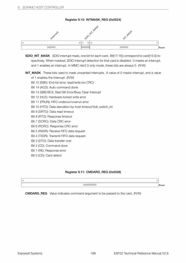
9. SD/MMC HOST CONTROLLER
Register 9.10: INTMASK_REG (0x0024)
(rese
rved)
0x00000
31 18
SDIO_IN
T_M
ASK
0x00000
17 16
INT_
MASK
0x00000
15 0
Reset
SDIO_INT_MASK SDIO interrupt mask, one bit for each card. Bit[17:16] correspond to card[15:0] re-
spectively. When masked, SDIO interrupt detection for that card is disabled. 0 masks an interrupt,
and 1 enables an interrupt. In MMC-Ver3.3-only mode, these bits are always 0. (R/W)
INT_MASK These bits used to mask unwanted interrupts. A value of 0 masks interrupt, and a value
of 1 enables the interrupt. (R/W)
Bit 15 (EBE): End-bit error, read/write (no CRC)
Bit 14 (ACD): Auto command done
Bit 13 (SBE/BCI): Start Bit Error/Busy Clear Interrupt
Bit 12 (HLE): Hardware locked write error
Bit 11 (FRUN): FIFO underrun/overrun error
Bit 10 (HTO): Data starvation-by-host timeout/Volt_switch_int
Bit 9 (DRTO): Data read timeout
Bit 8 (RTO): Response timeout
Bit 7 (DCRC): Data CRC error
Bit 6 (RCRC): Response CRC error
Bit 5 (RXDR): Receive FIFO data request
Bit 4 (TXDR): Transmit FIFO data request
Bit 3 (DTO): Data transfer over
Bit 2 (CD): Command done
Bit 1 (RE): Response error
Bit 0 (CD): Card detect
Register 9.11: CMDARG_REG (0x0028)
0x000000000
31 0
Reset
CMDARG_REG Value indicates command argument to be passed to the card. (R/W)
Espressif Systems 198 ESP32 Technical Reference Manual V2.8
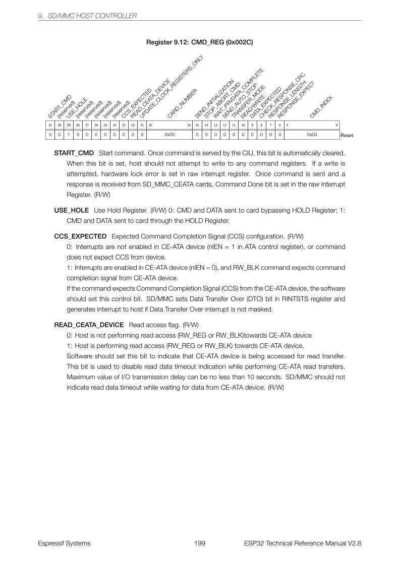
9. SD/MMC HOST CONTROLLER
Register 9.12: CMD_REG (0x002C)
START_
CMD
0
31
(rese
rved)
0
30
USE_HOLE
1
29
(rese
rved)
0
28
(rese
rved)
0
27
(rese
rved)
0
26
(rese
rved)
0
25
(rese
rved)
0
24
CCS_EXP
ECTED
0
23
READ_CEAT
A_DEVIC
E
0
22
UPDATE_C
LOCK_R
EGISTE
RS_ONLY
0
21
CARD_NUM
BER
0x00
20 16
SEND_INITI
ALIZAT
ION
0
15
STOP_A
BORT_CM
D
0
14
WAIT_
PRVDATA_C
OMPLE
TE
0
13
SEND_AUTO
_STO
P
0
12
TRANSFE
R_MODE
0
11
READ/WRITE
0
10
DATA_E
XPECTE
D
0
9
CHECK_RESPONSE_C
RC
0
8
RESPONSE_LENGTH
0
7
RESPONSE_EXP
ECT
0
6
CMD_IN
DEX
0x00
5 0
Reset
START_CMD Start command. Once command is served by the CIU, this bit is automatically cleared.
When this bit is set, host should not attempt to write to any command registers. If a write is
attempted, hardware lock error is set in raw interrupt register. Once command is sent and a
response is received from SD_MMC_CEATA cards, Command Done bit is set in the raw interrupt
Register. (R/W)
USE_HOLE Use Hold Register. (R/W) 0: CMD and DATA sent to card bypassing HOLD Register; 1:
CMD and DATA sent to card through the HOLD Register.
CCS_EXPECTED Expected Command Completion Signal (CCS) configuration. (R/W)
0: Interrupts are not enabled in CE-ATA device (nIEN = 1 in ATA control register), or command
does not expect CCS from device.
1: Interrupts are enabled in CE-ATA device (nIEN = 0), and RW_BLK command expects command
completion signal from CE-ATA device.
If the command expects Command Completion Signal (CCS) from the CE-ATA device, the software
should set this control bit. SD/MMC sets Data Transfer Over (DTO) bit in RINTSTS register and
generates interrupt to host if Data Transfer Over interrupt is not masked.
READ_CEATA_DEVICE Read access flag. (R/W)
0: Host is not performing read access (RW_REG or RW_BLK)towards CE-ATA device
1: Host is performing read access (RW_REG or RW_BLK) towards CE-ATA device.
Software should set this bit to indicate that CE-ATA device is being accessed for read transfer.
This bit is used to disable read data timeout indication while performing CE-ATA read transfers.
Maximum value of I/O transmission delay can be no less than 10 seconds. SD/MMC should not
indicate read data timeout while waiting for data from CE-ATA device. (R/W)
Espressif Systems 199 ESP32 Technical Reference Manual V2.8
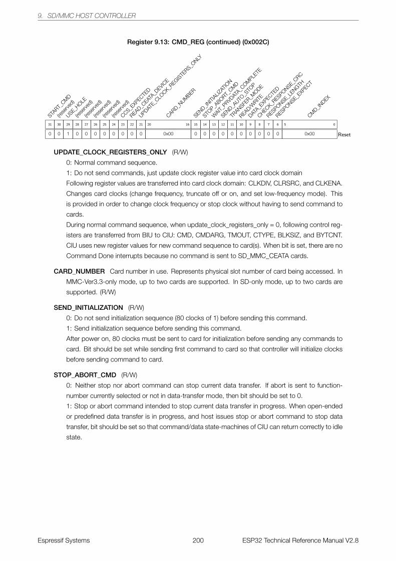
9. SD/MMC HOST CONTROLLER
Register 9.13: CMD_REG (continued) (0x002C)
START_
CMD
0
31
(rese
rved)
0
30
USE_HOLE
1
29
(rese
rved)
0
28
(rese
rved)
0
27
(rese
rved)
0
26
(rese
rved)
0
25
(rese
rved)
0
24
CCS_EXP
ECTED
0
23
READ_CEAT
A_DEVIC
E
0
22
UPDATE_C
LOCK_R
EGISTE
RS_ONLY
0
21
CARD_NUM
BER
0x00
20 16
SEND_INITI
ALIZAT
ION
0
15
STOP_A
BORT_CM
D
0
14
WAIT_
PRVDATA_C
OMPLE
TE
0
13
SEND_AUTO
_STO
P
0
12
TRANSFE
R_MODE
0
11
READ/WRITE
0
10
DATA_E
XPECTE
D
0
9
CHECK_RESPONSE_C
RC
0
8
RESPONSE_LENGTH
0
7
RESPONSE_EXP
ECT
0
6
CMD_IN
DEX
0x00
5 0
Reset
UPDATE_CLOCK_REGISTERS_ONLY (R/W)
0: Normal command sequence.
1: Do not send commands, just update clock register value into card clock domain
Following register values are transferred into card clock domain: CLKDIV, CLRSRC, and CLKENA.
Changes card clocks (change frequency, truncate off or on, and set low-frequency mode). This
is provided in order to change clock frequency or stop clock without having to send command to
cards.
During normal command sequence, when update_clock_registers_only = 0, following control reg-
isters are transferred from BIU to CIU: CMD, CMDARG, TMOUT, CTYPE, BLKSIZ, and BYTCNT.
CIU uses new register values for new command sequence to card(s). When bit is set, there are no
Command Done interrupts because no command is sent to SD_MMC_CEATA cards.
CARD_NUMBER Card number in use. Represents physical slot number of card being accessed. In
MMC-Ver3.3-only mode, up to two cards are supported. In SD-only mode, up to two cards are
supported. (R/W)
SEND_INITIALIZATION (R/W)
0: Do not send initialization sequence (80 clocks of 1) before sending this command.
1: Send initialization sequence before sending this command.
After power on, 80 clocks must be sent to card for initialization before sending any commands to
card. Bit should be set while sending first command to card so that controller will initialize clocks
before sending command to card.
STOP_ABORT_CMD (R/W)
0: Neither stop nor abort command can stop current data transfer. If abort is sent to function-
number currently selected or not in data-transfer mode, then bit should be set to 0.
1: Stop or abort command intended to stop current data transfer in progress. When open-ended
or predefined data transfer is in progress, and host issues stop or abort command to stop data
transfer, bit should be set so that command/data state-machines of CIU can return correctly to idle
state.
Espressif Systems 200 ESP32 Technical Reference Manual V2.8
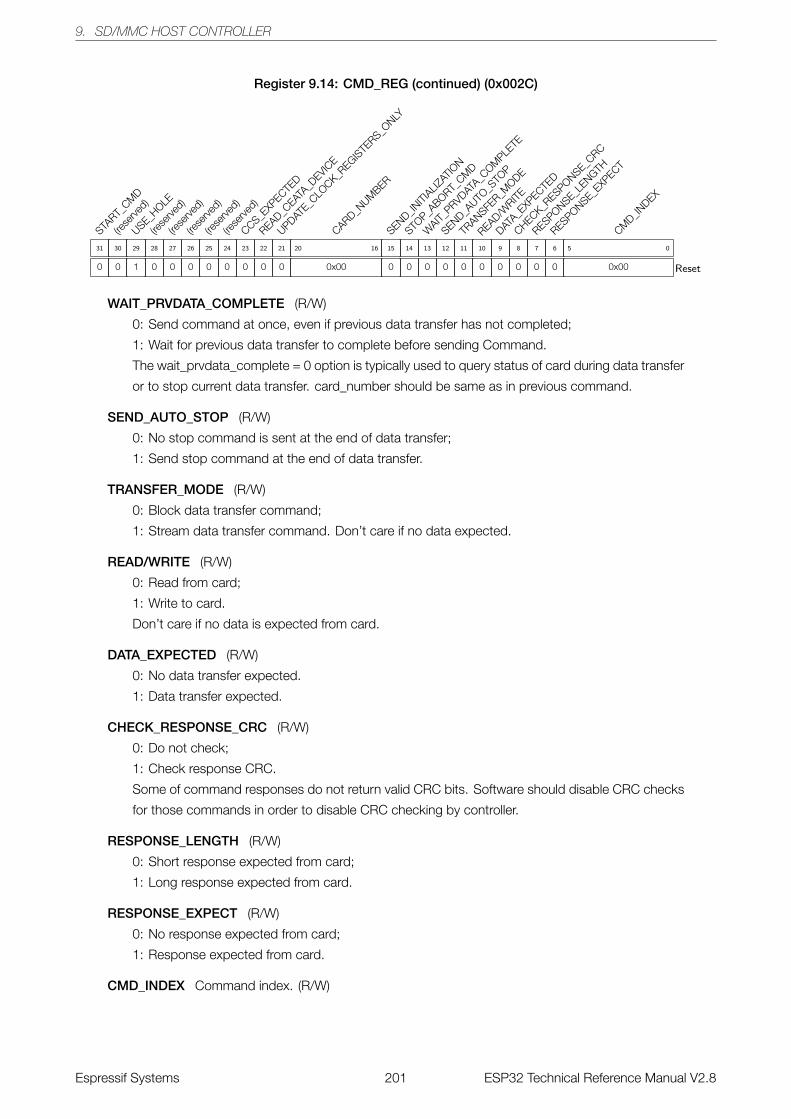
9. SD/MMC HOST CONTROLLER
Register 9.14: CMD_REG (continued) (0x002C)
START_
CMD
0
31
(rese
rved)
0
30
USE_HOLE
1
29
(rese
rved)
0
28
(rese
rved)
0
27
(rese
rved)
0
26
(rese
rved)
0
25
(rese
rved)
0
24
CCS_EXP
ECTED
0
23
READ_CEAT
A_DEVIC
E
0
22
UPDATE_C
LOCK_R
EGISTE
RS_ONLY
0
21
CARD_NUM
BER
0x00
20 16
SEND_INITI
ALIZAT
ION
0
15
STOP_A
BORT_CM
D
0
14
WAIT_
PRVDATA_C
OMPLE
TE
0
13
SEND_AUTO
_STO
P
0
12
TRANSFE
R_MODE
0
11
READ/WRITE
0
10
DATA_E
XPECTE
D
0
9
CHECK_RESPONSE_C
RC
0
8
RESPONSE_LENGTH
0
7
RESPONSE_EXP
ECT
0
6
CMD_IN
DEX
0x00
5 0
Reset
WAIT_PRVDATA_COMPLETE (R/W)
0: Send command at once, even if previous data transfer has not completed;
1: Wait for previous data transfer to complete before sending Command.
The wait_prvdata_complete = 0 option is typically used to query status of card during data transfer
or to stop current data transfer. card_number should be same as in previous command.
SEND_AUTO_STOP (R/W)
0: No stop command is sent at the end of data transfer;
1: Send stop command at the end of data transfer.
TRANSFER_MODE (R/W)
0: Block data transfer command;
1: Stream data transfer command. Don’t care if no data expected.
READ/WRITE (R/W)
0: Read from card;
1: Write to card.
Don’t care if no data is expected from card.
DATA_EXPECTED (R/W)
0: No data transfer expected.
1: Data transfer expected.
CHECK_RESPONSE_CRC (R/W)
0: Do not check;
1: Check response CRC.
Some of command responses do not return valid CRC bits. Software should disable CRC checks
for those commands in order to disable CRC checking by controller.
RESPONSE_LENGTH (R/W)
0: Short response expected from card;
1: Long response expected from card.
RESPONSE_EXPECT (R/W)
0: No response expected from card;
1: Response expected from card.
CMD_INDEX Command index. (R/W)
Espressif Systems 201 ESP32 Technical Reference Manual V2.8
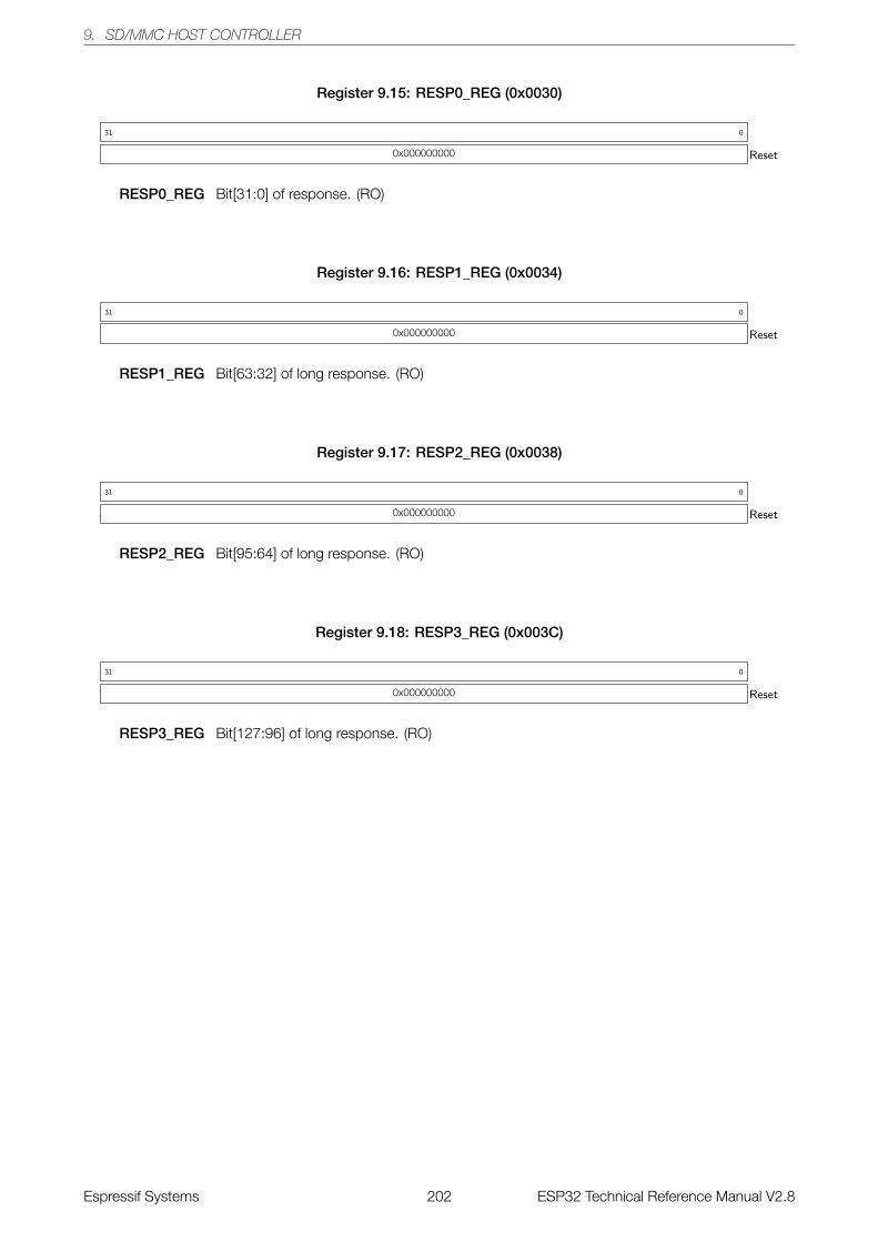
9. SD/MMC HOST CONTROLLER
Register 9.15: RESP0_REG (0x0030)
0x000000000
31 0
Reset
RESP0_REG Bit[31:0] of response. (RO)
Register 9.16: RESP1_REG (0x0034)
0x000000000
31 0
Reset
RESP1_REG Bit[63:32] of long response. (RO)
Register 9.17: RESP2_REG (0x0038)
0x000000000
31 0
Reset
RESP2_REG Bit[95:64] of long response. (RO)
Register 9.18: RESP3_REG (0x003C)
0x000000000
31 0
Reset
RESP3_REG Bit[127:96] of long response. (RO)
Espressif Systems 202 ESP32 Technical Reference Manual V2.8
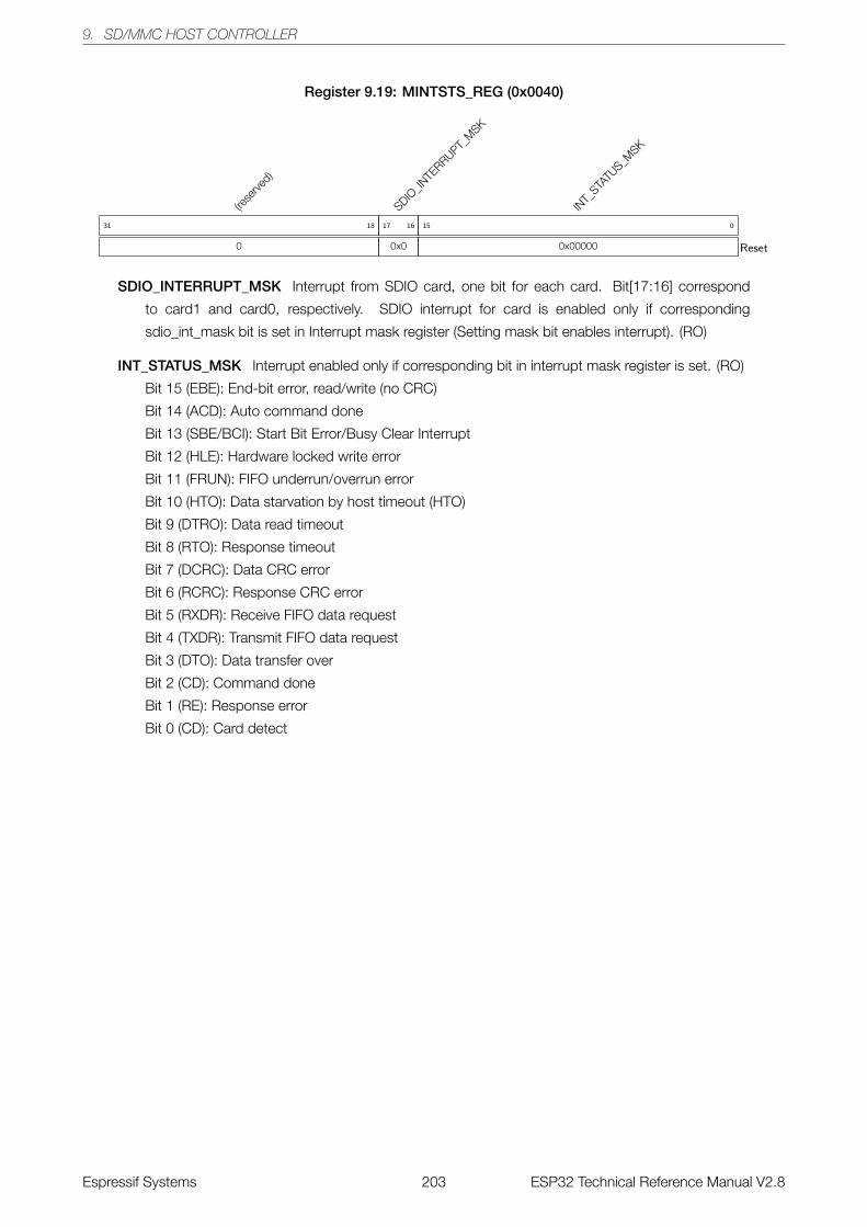
9. SD/MMC HOST CONTROLLER
Register 9.19: MINTSTS_REG (0x0040)
(rese
rved)
0
31 18
SDIO_IN
TERRUPT_
MSK
0x0
17 16
INT_
STATU
S_MSK
0x00000
15 0
Reset
SDIO_INTERRUPT_MSK Interrupt from SDIO card, one bit for each card. Bit[17:16] correspond
to card1 and card0, respectively. SDIO interrupt for card is enabled only if corresponding
sdio_int_mask bit is set in Interrupt mask register (Setting mask bit enables interrupt). (RO)
INT_STATUS_MSK Interrupt enabled only if corresponding bit in interrupt mask register is set. (RO)
Bit 15 (EBE): End-bit error, read/write (no CRC)
Bit 14 (ACD): Auto command done
Bit 13 (SBE/BCI): Start Bit Error/Busy Clear Interrupt
Bit 12 (HLE): Hardware locked write error
Bit 11 (FRUN): FIFO underrun/overrun error
Bit 10 (HTO): Data starvation by host timeout (HTO)
Bit 9 (DTRO): Data read timeout
Bit 8 (RTO): Response timeout
Bit 7 (DCRC): Data CRC error
Bit 6 (RCRC): Response CRC error
Bit 5 (RXDR): Receive FIFO data request
Bit 4 (TXDR): Transmit FIFO data request
Bit 3 (DTO): Data transfer over
Bit 2 (CD): Command done
Bit 1 (RE): Response error
Bit 0 (CD): Card detect
Espressif Systems 203 ESP32 Technical Reference Manual V2.8
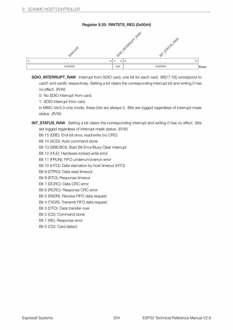
9. SD/MMC HOST CONTROLLER
Register 9.20: RINTSTS_REG (0x0044)
(rese
rved)
0x00000
31 16
SDIO_IN
TERRUPT_
RAW
0x0
17 16
INT_
STATU
S_RAW
0x00000
31 18
Reset
SDIO_INTERRUPT_RAW Interrupt from SDIO card, one bit for each card. Bit[17:16] correspond to
card1 and card0, respectively. Setting a bit clears the corresponding interrupt bit and writing 0 has
no effect. (R/W)
0: No SDIO interrupt from card;
1: SDIO interrupt from card.
In MMC-Ver3.3-only mode, these bits are always 0. Bits are logged regardless of interrupt-mask
status. (R/W)
INT_STATUS_RAW Setting a bit clears the corresponding interrupt and writing 0 has no effect. Bits
are logged regardless of interrupt mask status. (R/W)
Bit 15 (EBE): End-bit error, read/write (no CRC)
Bit 14 (ACD): Auto command done
Bit 13 (SBE/BCI): Start Bit Error/Busy Clear Interrupt
Bit 12 (HLE): Hardware locked write error
Bit 11 (FRUN): FIFO underrun/overrun error
Bit 10 (HTO): Data starvation by host timeout (HTO)
Bit 9 (DTRO): Data read timeout
Bit 8 (RTO): Response timeout
Bit 7 (DCRC): Data CRC error
Bit 6 (RCRC): Response CRC error
Bit 5 (RXDR): Receive FIFO data request
Bit 4 (TXDR): Transmit FIFO data request
Bit 3 (DTO): Data transfer over
Bit 2 (CD): Command done
Bit 1 (RE): Response error
Bit 0 (CD): Card detect
Espressif Systems 204 ESP32 Technical Reference Manual V2.8
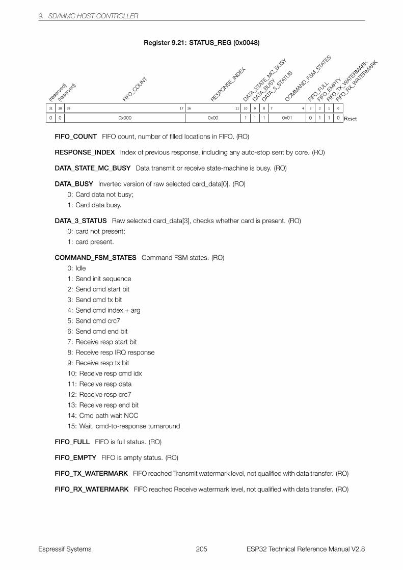
9. SD/MMC HOST CONTROLLER
Register 9.21: STATUS_REG (0x0048)
(rese
rved)
0
31
(rese
rved)
0
30
FIFO_C
OUNT
0x000
29 17
RESPONSE_INDEX
0x00
16 11
DATA_S
TATE
_MC_B
USY
1
10
DATA_B
USY
1
9
DATA_3
_STA
TUS
1
8
COMM
AND_FSM
_STA
TES
0x01
7 4
FIFO_F
ULL
0
3
FIFO_E
MPTY
1
2
FIFO_T
X_W
ATERM
ARK
1
1
FIFO_R
X_W
ATERM
ARK
0
0
Reset
FIFO_COUNT FIFO count, number of filled locations in FIFO. (RO)
RESPONSE_INDEX Index of previous response, including any auto-stop sent by core. (RO)
DATA_STATE_MC_BUSY Data transmit or receive state-machine is busy. (RO)
DATA_BUSY Inverted version of raw selected card_data[0]. (RO)
0: Card data not busy;
1: Card data busy.
DATA_3_STATUS Raw selected card_data[3], checks whether card is present. (RO)
0: card not present;
1: card present.
COMMAND_FSM_STATES Command FSM states. (RO)
0: Idle
1: Send init sequence
2: Send cmd start bit
3: Send cmd tx bit
4: Send cmd index + arg
5: Send cmd crc7
6: Send cmd end bit
7: Receive resp start bit
8: Receive resp IRQ response
9: Receive resp tx bit
10: Receive resp cmd idx
11: Receive resp data
12: Receive resp crc7
13: Receive resp end bit
14: Cmd path wait NCC
15: Wait, cmd-to-response turnaround
FIFO_FULL FIFO is full status. (RO)
FIFO_EMPTY FIFO is empty status. (RO)
FIFO_TX_WATERMARK FIFO reached Transmit watermark level, not qualified with data transfer. (RO)
FIFO_RX_WATERMARK FIFO reached Receive watermark level, not qualified with data transfer. (RO)
Espressif Systems 205 ESP32 Technical Reference Manual V2.8
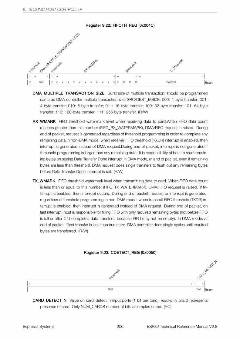
9. SD/MMC HOST CONTROLLER
Register 9.22: FIFOTH_REG (0x004C)
(rese
rved)
0
31
DMA_M
ULTIP
LE_T
RANSACTION_S
IZE
0x0
30 28
(rese
rved)
0
27
RX_W
MARK
x x x x x x x x x x x
26 16
(rese
rved)
0 0 0 0
15 12
TX_W
MARK
0x0000
11 0
Reset
DMA_MULTIPLE_TRANSACTION_SIZE Burst size of multiple transaction, should be programmed
same as DMA controller multiple-transaction-size SRC/DEST_MSIZE. 000: 1-byte transfer; 001:
4-byte transfer; 010: 8-byte transfer; 011: 16-byte transfer; 100: 32-byte transfer; 101: 64-byte
transfer; 110: 128-byte transfer; 111: 256-byte transfer. (R/W)
RX_WMARK FIFO threshold watermark level when receiving data to card.When FIFO data count
reaches greater than this number (FIFO_RX_WATERMARK), DMA/FIFO request is raised. During
end of packet, request is generated regardless of threshold programming in order to complete any
remaining data.In non-DMA mode, when receiver FIFO threshold (RXDR) interrupt is enabled, then
interrupt is generated instead of DMA request.During end of packet, interrupt is not generated if
threshold programming is larger than any remaining data. It is responsibility of host to read remain-
ing bytes on seeing Data Transfer Done interrupt.In DMA mode, at end of packet, even if remaining
bytes are less than threshold, DMA request does single transfers to flush out any remaining bytes
before Data Transfer Done interrupt is set. (R/W)
TX_WMARK FIFO threshold watermark level when transmitting data to card. When FIFO data count
is less than or equal to this number (FIFO_TX_WATERMARK), DMA/FIFO request is raised. If In-
terrupt is enabled, then interrupt occurs. During end of packet, request or interrupt is generated,
regardless of threshold programming.In non-DMA mode, when transmit FIFO threshold (TXDR) in-
terrupt is enabled, then interrupt is generated instead of DMA request. During end of packet, on
last interrupt, host is responsible for filling FIFO with only required remaining bytes (not before FIFO
is full or after CIU completes data transfers, because FIFO may not be empty). In DMA mode, at
end of packet, if last transfer is less than burst size, DMA controller does single cycles until required
bytes are transferred. (R/W)
Register 9.23: CDETECT_REG (0x0050)
(rese
rved)
0x0
31 2
CARD_DETE
CT_N
0x0
1 0
Reset
CARD_DETECT_N Value on card_detect_n input ports (1 bit per card), read-only bits.0 represents
presence of card. Only NUM_CARDS number of bits are implemented. (RO)
Espressif Systems 206 ESP32 Technical Reference Manual V2.8
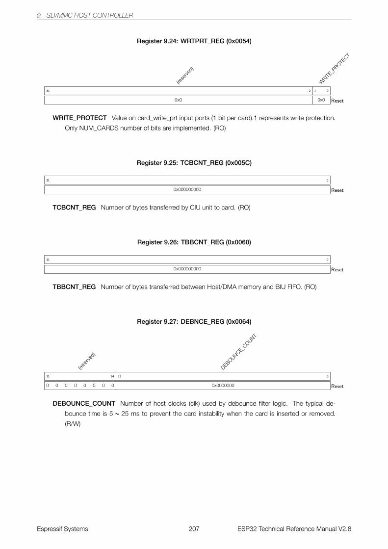
9. SD/MMC HOST CONTROLLER
Register 9.24: WRTPRT_REG (0x0054)
(rese
rved)
0x0
31 2
WRITE
_PROTE
CT
0x0
1 0
Reset
WRITE_PROTECT Value on card_write_prt input ports (1 bit per card).1 represents write protection.
Only NUM_CARDS number of bits are implemented. (RO)
Register 9.25: TCBCNT_REG (0x005C)
0x000000000
31 0
Reset
TCBCNT_REG Number of bytes transferred by CIU unit to card. (RO)
Register 9.26: TBBCNT_REG (0x0060)
0x000000000
31 0
Reset
TBBCNT_REG Number of bytes transferred between Host/DMA memory and BIU FIFO. (RO)
Register 9.27: DEBNCE_REG (0x0064)
(rese
rved)
0 0 0 0 0 0 0 0
31 24
DEBOUNCE_COUNT
0x0000000
23 0
Reset
DEBOUNCE_COUNT Number of host clocks (clk) used by debounce filter logic. The typical de-
bounce time is 5 ~ 25 ms to prevent the card instability when the card is inserted or removed.
(R/W)
Espressif Systems 207 ESP32 Technical Reference Manual V2.8
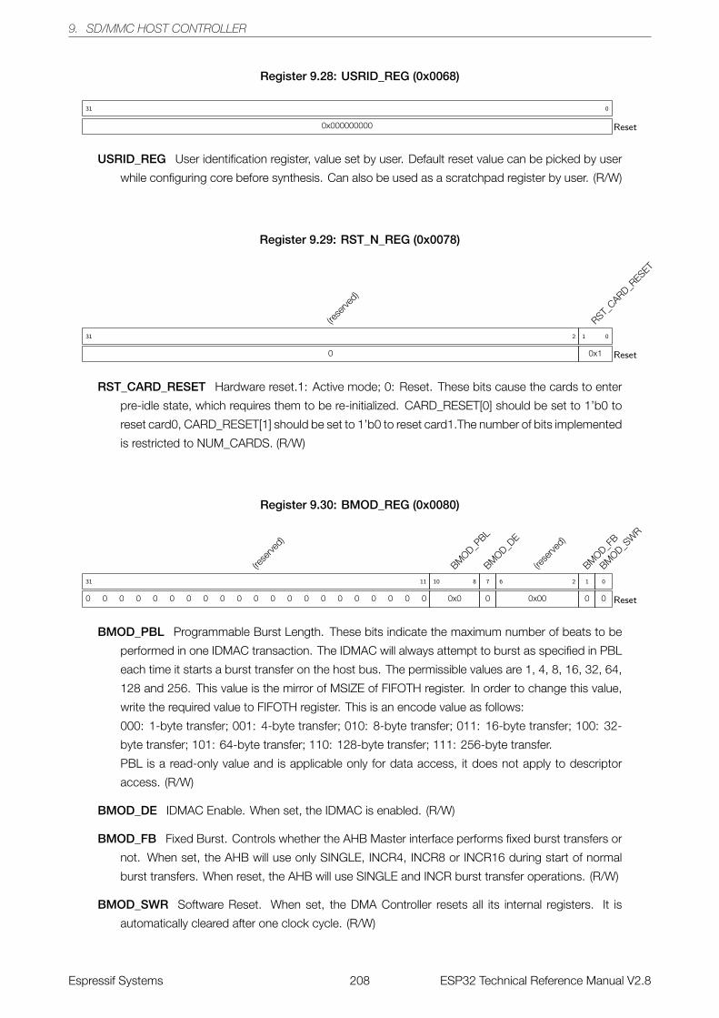
9. SD/MMC HOST CONTROLLER
Register 9.28: USRID_REG (0x0068)
0x000000000
31 0
Reset
USRID_REG User identification register, value set by user. Default reset value can be picked by user
while configuring core before synthesis. Can also be used as a scratchpad register by user. (R/W)
Register 9.29: RST_N_REG (0x0078)
(rese
rved)
0
31 2
RST_CARD_R
ESET
0x1
1 0
Reset
RST_CARD_RESET Hardware reset.1: Active mode; 0: Reset. These bits cause the cards to enter
pre-idle state, which requires them to be re-initialized. CARD_RESET[0] should be set to 1’b0 to
reset card0, CARD_RESET[1] should be set to 1’b0 to reset card1.The number of bits implemented
is restricted to NUM_CARDS. (R/W)
Register 9.30: BMOD_REG (0x0080)
(rese
rved)
0 0 0 0 0 0 0 0 0 0 0 0 0 0 0 0 0 0 0 0 0
31 11
BMOD_P
BL
0x0
10 8
BMOD_D
E
0
7
(rese
rved)
0x00
6 2
BMOD_F
B
0
1
BMOD_S
WR
0
0
Reset
BMOD_PBL Programmable Burst Length. These bits indicate the maximum number of beats to be
performed in one IDMAC transaction. The IDMAC will always attempt to burst as specified in PBL
each time it starts a burst transfer on the host bus. The permissible values are 1, 4, 8, 16, 32, 64,
128 and 256. This value is the mirror of MSIZE of FIFOTH register. In order to change this value,
write the required value to FIFOTH register. This is an encode value as follows:
000: 1-byte transfer; 001: 4-byte transfer; 010: 8-byte transfer; 011: 16-byte transfer; 100: 32-
byte transfer; 101: 64-byte transfer; 110: 128-byte transfer; 111: 256-byte transfer.
PBL is a read-only value and is applicable only for data access, it does not apply to descriptor
access. (R/W)
BMOD_DE IDMAC Enable. When set, the IDMAC is enabled. (R/W)
BMOD_FB Fixed Burst. Controls whether the AHB Master interface performs fixed burst transfers or
not. When set, the AHB will use only SINGLE, INCR4, INCR8 or INCR16 during start of normal
burst transfers. When reset, the AHB will use SINGLE and INCR burst transfer operations. (R/W)
BMOD_SWR Software Reset. When set, the DMA Controller resets all its internal registers. It is
automatically cleared after one clock cycle. (R/W)
Espressif Systems 208 ESP32 Technical Reference Manual V2.8
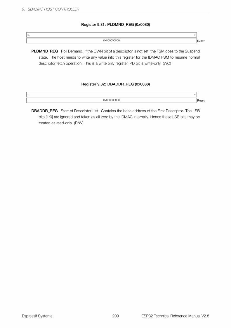
9. SD/MMC HOST CONTROLLER
Register 9.31: PLDMND_REG (0x0080)
0x000000000
31 0
Reset
PLDMND_REG Poll Demand. If the OWN bit of a descriptor is not set, the FSM goes to the Suspend
state. The host needs to write any value into this register for the IDMAC FSM to resume normal
descriptor fetch operation. This is a write only register, PD bit is write-only. (WO)
Register 9.32: DBADDR_REG (0x0088)
0x000000000
31 0
Reset
DBADDR_REG Start of Descriptor List. Contains the base address of the First Descriptor. The LSB
bits [1:0] are ignored and taken as all-zero by the IDMAC internally. Hence these LSB bits may be
treated as read-only. (R/W)
Espressif Systems 209 ESP32 Technical Reference Manual V2.8
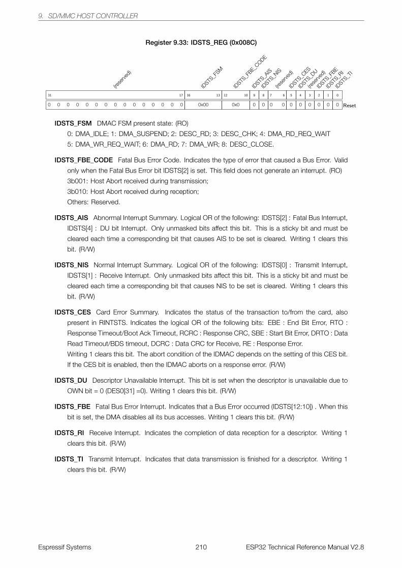
9. SD/MMC HOST CONTROLLER
Register 9.33: IDSTS_REG (0x008C)
(rese
rved)
0 0 0 0 0 0 0 0 0 0 0 0 0 0 0
31 17
IDSTS
_FSM
0x00
16 13
IDSTS
_FBE_C
ODE
0x0
12 10
IDSTS
_AIS
0
9
IDSTS
_NIS
0
8
(rese
rved)
0 0
7 6
IDSTS
_CES
0
5
IDSTS
_DU
0
4
(rese
rved)
0
3
IDSTS
_FBE
0
2
IDSTS
_RI
0
1
IDSTS
_TI
0
0
Reset
IDSTS_FSM DMAC FSM present state: (RO)
0: DMA_IDLE; 1: DMA_SUSPEND; 2: DESC_RD; 3: DESC_CHK; 4: DMA_RD_REQ_WAIT
5: DMA_WR_REQ_WAIT; 6: DMA_RD; 7: DMA_WR; 8: DESC_CLOSE.
IDSTS_FBE_CODE Fatal Bus Error Code. Indicates the type of error that caused a Bus Error. Valid
only when the Fatal Bus Error bit IDSTS[2] is set. This field does not generate an interrupt. (RO)
3b001: Host Abort received during transmission;
3b010: Host Abort received during reception;
Others: Reserved.
IDSTS_AIS Abnormal Interrupt Summary. Logical OR of the following: IDSTS[2] : Fatal Bus Interrupt,
IDSTS[4] : DU bit Interrupt. Only unmasked bits affect this bit. This is a sticky bit and must be
cleared each time a corresponding bit that causes AIS to be set is cleared. Writing 1 clears this
bit. (R/W)
IDSTS_NIS Normal Interrupt Summary. Logical OR of the following: IDSTS[0] : Transmit Interrupt,
IDSTS[1] : Receive Interrupt. Only unmasked bits affect this bit. This is a sticky bit and must be
cleared each time a corresponding bit that causes NIS to be set is cleared. Writing 1 clears this
bit. (R/W)
IDSTS_CES Card Error Summary. Indicates the status of the transaction to/from the card, also
present in RINTSTS. Indicates the logical OR of the following bits: EBE : End Bit Error, RTO :
Response Timeout/Boot Ack Timeout, RCRC : Response CRC, SBE : Start Bit Error, DRTO : Data
Read Timeout/BDS timeout, DCRC : Data CRC for Receive, RE : Response Error.
Writing 1 clears this bit. The abort condition of the IDMAC depends on the setting of this CES bit.
If the CES bit is enabled, then the IDMAC aborts on a response error. (R/W)
IDSTS_DU Descriptor Unavailable Interrupt. This bit is set when the descriptor is unavailable due to
OWN bit = 0 (DES0[31] =0). Writing 1 clears this bit. (R/W)
IDSTS_FBE Fatal Bus Error Interrupt. Indicates that a Bus Error occurred (IDSTS[12:10]) . When this
bit is set, the DMA disables all its bus accesses. Writing 1 clears this bit. (R/W)
IDSTS_RI Receive Interrupt. Indicates the completion of data reception for a descriptor. Writing 1
clears this bit. (R/W)
IDSTS_TI Transmit Interrupt. Indicates that data transmission is finished for a descriptor. Writing 1
clears this bit. (R/W)
Espressif Systems 210 ESP32 Technical Reference Manual V2.8
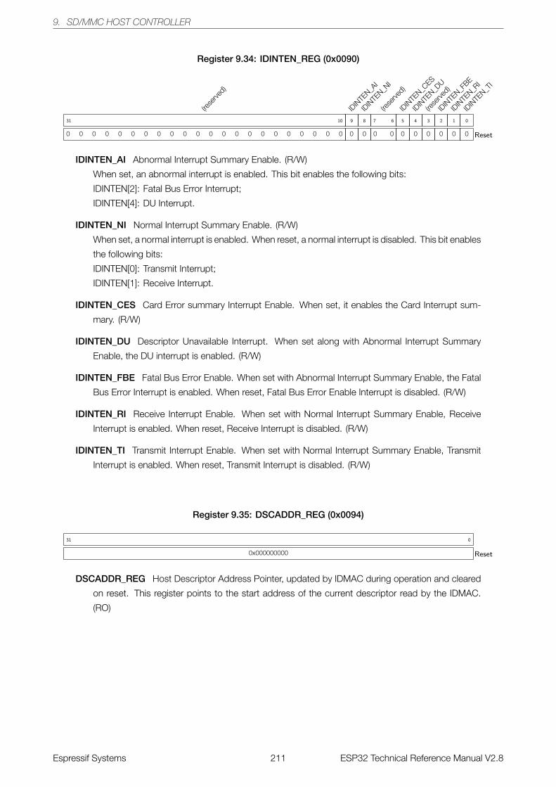
9. SD/MMC HOST CONTROLLER
Register 9.34: IDINTEN_REG (0x0090)
(rese
rved)
0 0 0 0 0 0 0 0 0 0 0 0 0 0 0 0 0 0 0 0 0 0
31 10
IDIN
TEN_A
I
0
9
IDIN
TEN_N
I
0
8
(rese
rved)
0 0
7 6
IDIN
TEN_C
ES
0
5
IDIN
TEN_D
U
0
4
(rese
rved)
0
3
IDIN
TEN_F
BE
0
2
IDIN
TEN_R
I
0
1
IDIN
TEN_T
I
0
0
Reset
IDINTEN_AI Abnormal Interrupt Summary Enable. (R/W)
When set, an abnormal interrupt is enabled. This bit enables the following bits:
IDINTEN[2]: Fatal Bus Error Interrupt;
IDINTEN[4]: DU Interrupt.
IDINTEN_NI Normal Interrupt Summary Enable. (R/W)
When set, a normal interrupt is enabled. When reset, a normal interrupt is disabled. This bit enables
the following bits:
IDINTEN[0]: Transmit Interrupt;
IDINTEN[1]: Receive Interrupt.
IDINTEN_CES Card Error summary Interrupt Enable. When set, it enables the Card Interrupt sum-
mary. (R/W)
IDINTEN_DU Descriptor Unavailable Interrupt. When set along with Abnormal Interrupt Summary
Enable, the DU interrupt is enabled. (R/W)
IDINTEN_FBE Fatal Bus Error Enable. When set with Abnormal Interrupt Summary Enable, the Fatal
Bus Error Interrupt is enabled. When reset, Fatal Bus Error Enable Interrupt is disabled. (R/W)
IDINTEN_RI Receive Interrupt Enable. When set with Normal Interrupt Summary Enable, Receive
Interrupt is enabled. When reset, Receive Interrupt is disabled. (R/W)
IDINTEN_TI Transmit Interrupt Enable. When set with Normal Interrupt Summary Enable, Transmit
Interrupt is enabled. When reset, Transmit Interrupt is disabled. (R/W)
Register 9.35: DSCADDR_REG (0x0094)
0x000000000
31 0
Reset
DSCADDR_REG Host Descriptor Address Pointer, updated by IDMAC during operation and cleared
on reset. This register points to the start address of the current descriptor read by the IDMAC.
(RO)
Espressif Systems 211 ESP32 Technical Reference Manual V2.8
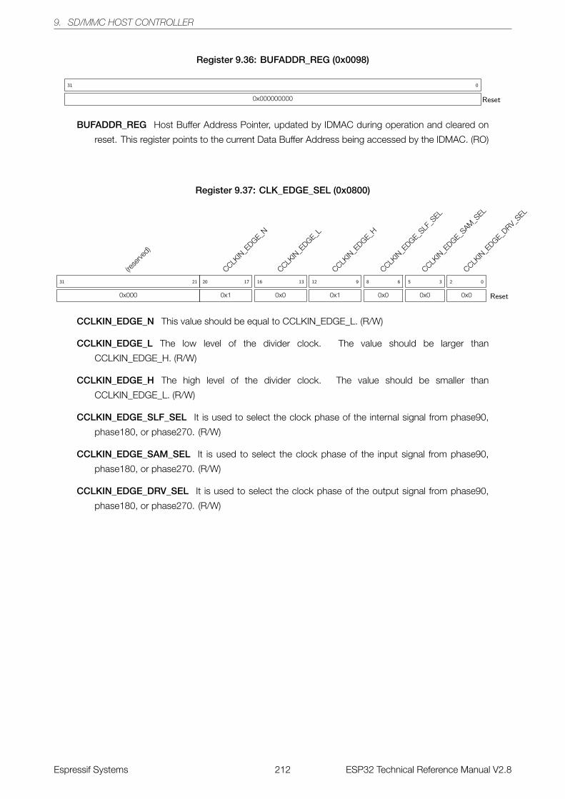
9. SD/MMC HOST CONTROLLER
Register 9.36: BUFADDR_REG (0x0098)
0x000000000
31 0
Reset
BUFADDR_REG Host Buffer Address Pointer, updated by IDMAC during operation and cleared on
reset. This register points to the current Data Buffer Address being accessed by the IDMAC. (RO)
Register 9.37: CLK_EDGE_SEL (0x0800)
(rese
rved)
0x000
31 21
CCLKIN
_EDGE_N
0x1
20 17
CCLKIN
_EDGE_L
0x0
16 13
CCLKIN
_EDGE_H
0x1
12 9
CCLKIN
_EDGE_S
LF_S
EL
0x0
8 6
CCLKIN
_EDGE_S
AM_S
EL
0x0
5 3
CCLKIN
_EDGE_D
RV_SEL
0x0
2 0
Reset
CCLKIN_EDGE_N This value should be equal to CCLKIN_EDGE_L. (R/W)
CCLKIN_EDGE_L The low level of the divider clock. The value should be larger than
CCLKIN_EDGE_H. (R/W)
CCLKIN_EDGE_H The high level of the divider clock. The value should be smaller than
CCLKIN_EDGE_L. (R/W)
CCLKIN_EDGE_SLF_SEL It is used to select the clock phase of the internal signal from phase90,
phase180, or phase270. (R/W)
CCLKIN_EDGE_SAM_SEL It is used to select the clock phase of the input signal from phase90,
phase180, or phase270. (R/W)
CCLKIN_EDGE_DRV_SEL It is used to select the clock phase of the output signal from phase90,
phase180, or phase270. (R/W)
Espressif Systems 212 ESP32 Technical Reference Manual V2.8
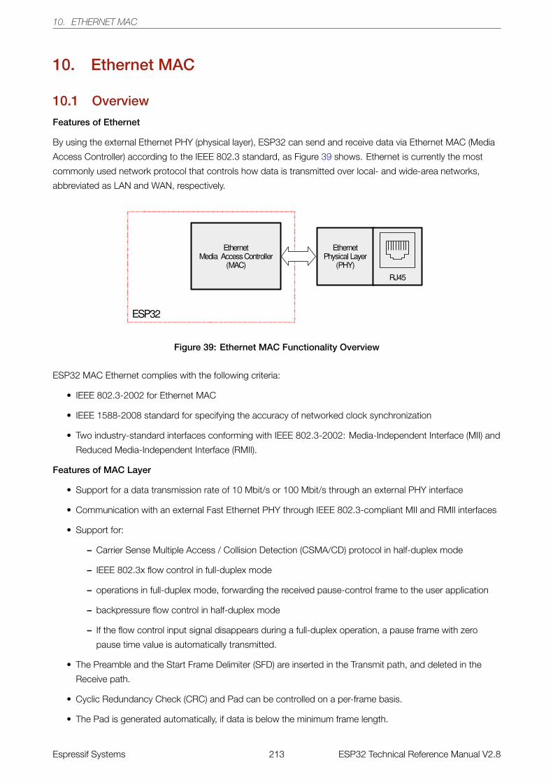
10. ETHERNET MAC
10. Ethernet MAC
10.1 Overview
Features of Ethernet
By using the external Ethernet PHY (physical layer), ESP32 can send and receive data via Ethernet MAC (Media
Access Controller) according to the IEEE 802.3 standard, as Figure 39 shows. Ethernet is currently the most
commonly used network protocol that controls how data is transmitted over local- and wide-area networks,
abbreviated as LAN and WAN, respectively.
Figure 39: Ethernet MAC Functionality Overview
ESP32 MAC Ethernet complies with the following criteria:
• IEEE 802.3-2002 for Ethernet MAC
• IEEE 1588-2008 standard for specifying the accuracy of networked clock synchronization
• Two industry-standard interfaces conforming with IEEE 802.3-2002: Media-Independent Interface (MII) and
Reduced Media-Independent Interface (RMII).
Features of MAC Layer
• Support for a data transmission rate of 10 Mbit/s or 100 Mbit/s through an external PHY interface
• Communication with an external Fast Ethernet PHY through IEEE 802.3-compliant MII and RMII interfaces
• Support for:
– Carrier Sense Multiple Access / Collision Detection (CSMA/CD) protocol in half-duplex mode
– IEEE 802.3x flow control in full-duplex mode
– operations in full-duplex mode, forwarding the received pause-control frame to the user application
– backpressure flow control in half-duplex mode
– If the flow control input signal disappears during a full-duplex operation, a pause frame with zero
pause time value is automatically transmitted.
• The Preamble and the Start Frame Delimiter (SFD) are inserted in the Transmit path, and deleted in the
Receive path.
• Cyclic Redundancy Check (CRC) and Pad can be controlled on a per-frame basis.
• The Pad is generated automatically, if data is below the minimum frame length.
Espressif Systems 213 ESP32 Technical Reference Manual V2.8

10. ETHERNET MAC
• Programmable frame length supporting jumbo frames of up to 16 KB
• Programmable Inter-frame Gap (IFG) (40-96 bit times in steps of 8)
• Support for a variety of flexible address filtering modes:
– Up to eight 48-bit perfect address filters to mask each byte
– Up to eight 48-bit SA address comparison checks to mask each byte
– All multicast address frames can be transmitted
– All frames in mixed mode can be transmitted without being filtered for network monitoring
– A status report is attached each time all incoming packets are transmitted and filtered.
• Returning a 32-bit status for transmission and reception of packets respectively
• Separate transmission, reception, and control interfaces for the application
• Use of the Management Data Input/Output (MDIO) interface to configure and manage PHY devices
• Support for the offloading of received IPv4 and TCP packets encapsulated by an Ethernet frame in the
reception function
• Support for checking IPv4 header checksums, as well as TCP, UDP, or ICMP (Internet Control Message
Protocol) checksums encapsulated in IPv4/IPv6 packets in the enhanced reception function
• Support for Ethernet frame timestamps. (For details please refer to IEEE 1588-2008.) Each frame has a
64-bit timestamp when transmitted or received.
• Two sets of FIFOs: one 2 KB Tx FIFO with programmable threshold and one 2 KB Rx FIFO with
configurable threshold (64 bytes by default)
• When Rx FIFO stores multiple frames, the Receive Status Vector is inserted into the Rx FIFO after
transmitting an EOF (end of frame), so that the Rx FIFO does not need to store the Receive Status of these
frames.
• In store-and-forward mode, all error frames can be filtered during reception, but not forwarded to the
application.
• Under-sized good frames can be forwarded.
• Support for data statistics by generating pulses for lost or corrupted frames in the Rx FIFO due to an
overflow
• Support for store-and-forward mechanism when transmitting data to the MAC core
• Automatic re-transmission of collided frames during transmission (subject to certain conditions, see section
10.2.1.2)
• Discarding frames in cases of late collisions, excessive collisions, excessive deferrals, and under-run
conditions
• The Tx FIFO is flushed by software control.
• Calculating the IPv4 header checksum, as well as the TCP, UDP, or ICMP checksum, and then inserting
them into frames transmitted in store-and-forward mode.
Ethernet Block Diagram
Figure 40 shows the block diagram of the Ethernet.
Espressif Systems 214 ESP32 Technical Reference Manual V2.8
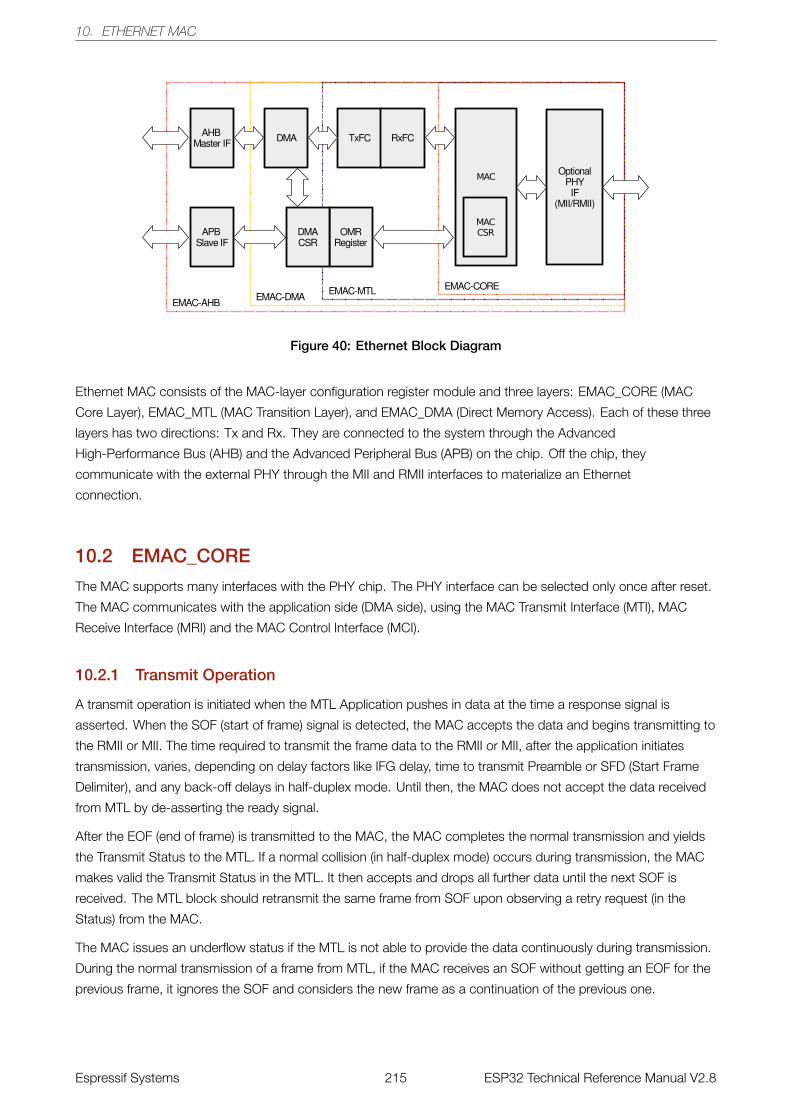
10. ETHERNET MAC
Figure 40: Ethernet Block Diagram
Ethernet MAC consists of the MAC-layer configuration register module and three layers: EMAC_CORE (MAC
Core Layer), EMAC_MTL (MAC Transition Layer), and EMAC_DMA (Direct Memory Access). Each of these three
layers has two directions: Tx and Rx. They are connected to the system through the Advanced
High-Performance Bus (AHB) and the Advanced Peripheral Bus (APB) on the chip. Off the chip, they
communicate with the external PHY through the MII and RMII interfaces to materialize an Ethernet
connection.
10.2 EMAC_CORE
The MAC supports many interfaces with the PHY chip. The PHY interface can be selected only once after reset.
The MAC communicates with the application side (DMA side), using the MAC Transmit Interface (MTI), MAC
Receive Interface (MRI) and the MAC Control Interface (MCI).
10.2.1 Transmit Operation
A transmit operation is initiated when the MTL Application pushes in data at the time a response signal is
asserted. When the SOF (start of frame) signal is detected, the MAC accepts the data and begins transmitting to
the RMII or MII. The time required to transmit the frame data to the RMII or MII, after the application initiates
transmission, varies, depending on delay factors like IFG delay, time to transmit Preamble or SFD (Start Frame
Delimiter), and any back-off delays in half-duplex mode. Until then, the MAC does not accept the data received
from MTL by de-asserting the ready signal.
After the EOF (end of frame) is transmitted to the MAC, the MAC completes the normal transmission and yields
the Transmit Status to the MTL. If a normal collision (in half-duplex mode) occurs during transmission, the MAC
makes valid the Transmit Status in the MTL. It then accepts and drops all further data until the next SOF is
received. The MTL block should retransmit the same frame from SOF upon observing a retry request (in the
Status) from the MAC.
The MAC issues an underflow status if the MTL is not able to provide the data continuously during transmission.
During the normal transmission of a frame from MTL, if the MAC receives an SOF without getting an EOF for the
previous frame, it ignores the SOF and considers the new frame as a continuation of the previous one.
Espressif Systems 215 ESP32 Technical Reference Manual V2.8
10. ETHERNET MAC
10.2.1.1 Transmit Flow Control
In full-duplex mode, when the Transmit Flow Control Enable bit (TFE bit in the Flow Control Register) is set to 1,
the MAC will generate and send a pause frame, as needed. The pause frame is added and transmitted together
with the calculated CRC. The generation of pause frames can be initiated in two ways.
When the application sets the Flow Control Busy bit (FCB bit in the Flow Control Register) to 1, or when the Rx
FIFO is full, a pause frame is transmitted.
• If an application has requested flow control by setting the FCB bit in the Flow Control Register to 1, the MAC
will generate and send a single pause frame. The pause time value in the generated frame is the pause time
value programmed in the Flow Control Register. To extend or end the pause time before the time specified
in the previously transmitted pause frame, the application program must configure the pause time value in
the Flow Control Register to the appropriate value and, then, request another pause frame transmission.
• If the application has requested flow control when the Rx FIFO is full, the MAC will generate and transmit a
pause frame. The value of the pause time of the generated frame is the pause time value programmed in
the Flow Control Register. If the Rx FIFO remains full during the configurable interval, which is determined
by the Pause Low Threshold bit (PLT) in the Flow Control Register before the pause time expires, a second
pause frame will be transmitted. As long as the Rx FIFO remains full, the process repeats itself. If the FIFO
is no longer full before the sample time, the MAC will send a pause frame with zero pause time, indicating
to the remote end that the Rx buffer is ready to receive the new data frame.
10.2.1.2 Retransmission During a Collision
In half-duplex mode, a collision may occur on the MAC line interface when frames are transmitted to the MAC.
The MAC may even give a status to indicate a retry before the end of the frame is received. The retransmission is
then enabled and the frame is popped out from the FIFO. When more than 96 bytes are transmitted to the MAC
core, the FIFO controller frees the space in the FIFO, allowing the DMA to push more data into FIFO. This means
that data cannot be retransmitted after the threshold is exceeded or when the MAC core indicates that a late
collision has occurred.
The MAC transmitter may abort the transmission of a frame because of collision, Tx FIFO underflow, loss of
carrier, jabber timeout, no carrier, excessive deferral, and late collision. When frame transmission is aborted
because of collision, the MAC requests retransmission of the frame.
10.2.2 Receive Operation
A receive operation is initiated when the MAC detects an SFD on the RMII or MII. The MAC strips the Preamble
and SFD before processing the frame. The header fields are checked for the filtering and the FCS (Frame Check
Sequence) field used to verify the CRC for the frame. The received frame is stored in a shallow buffer until the
address filtering is performed. The frame is dropped in the MAC if it fails the address filtering.
The frame received by the MAC will be pushed into the Rx FIFO. Once the FIFO status exceeds the Receive
Threshold, configured by the Receive Threshold Control (RTC) bit in the Operation Mode register, the DMA can
initiate a preconfigured burst transmission to the AHB interface.
In the default pass-through mode, when the FIFO receives a complete packet or 64 bytes configured by the RTC
bit in the Operation Mode Register, the data pops up and its availability is notified to the DMA. After the DMA
initiates the transmission to the AHB interface, the data transmission continues from the FIFO until the complete
Espressif Systems 216 ESP32 Technical Reference Manual V2.8
10. ETHERNET MAC
packet is transmitted. Upon completing transmitting the EOF, the status word will pop up and be transmitted to
the DMA controller.
In the Rx FIFO Store-and-Forward mode (configured through the RSF or Receive Store and Forward bit in the
Operation Mode Register), only the valid frames are read and forwarded to the application. In the passthrough
mode, error frames are not discarded because the error status is received at the end of the frame. The start of
frame will have been read from the FIFO at that point.
10.2.2.1 Reception Protocol
After the receive module receives the packets, the Preamble and SFD of the received frames are removed. When
the SFD is detected, the MAC starts sending Ethernet frame data to the Rx FIFO, starting at the first byte
(destination address) following the SFD. This timestamp is passed on to the application, unless the MAC filters
out and drops the frame.
If the received frame length/type is less than 0x600 and the automatic CRC/Pad removal option is programmed
for the MAC, the MAC will send frame data to the Rx FIFO (the amount of data does not exceed the number
specified in the length/type field). Then MAC begins discarding the remaining section, including the FCS field. If
the frame length/type is greater than, or equal to, 0x600, the MAC will send all received Ethernet frame data to
the Rx FIFO, regardless of the programmed value of the automatic CRC removal option. By default, the MAC
watchdog timer is enabled, meaning that frames, including DA, SA, LT, data, pad and FCS, which exceed 2048
bytes, are cut off. This function can be disabled by programming the Watchdog Disable (WD) bit in the MAC
Configuration Register. However, even if the watchdog timer is disabled, frames longer than 16 KB will be cut off
and the watchdog timeout status will be given.
10.2.2.2 Receive Frame Controller
If the RA (Receive All) bit in the MAC Frame Filter Register is reset, the MAC will filter frames based on the
destination and source addresses. If the application decides not to receive any bad frames, such as runt frames
and CRC error frames, another level of filtering is needed. When a frame fails the filtering, the frame is discarded
and is not transmitted to the application. When the filter parameters are changed dynamically, if a frame fails the
DA and SA filterings, the remaining part of the frame is discarded and the Receive Status word is updated
immediately and, therefore, the zero frame length bit, CRC error bit, and runt frame error bit are set to 1. This
indicates that the frame has failed the filtering.
10.2.2.3 Receive Flow Control
The MAC will detect the received pause frame and pause transmission of frames for a specified delay within the
received pause frame (in full-duplex mode only). The Pause Frame Detect Function can be enabled or disabled
by the RFCE (Receive Flow Control Enable) bit in the Flow Control Register. When receive flow control is enabled,
it starts monitoring whether the destination address of the received frame matches the multicast address of the
control frame (0x0180 C200 0001). If a match is detected (i.e. the destination address of the received frame
matches the destination address of the reserved control frame), the MAC will determine whether to transmit the
received control frame to the application, according to the PCF (Pass Control Frames) bit in the Frame Filter
Register.
Espressif Systems 217 ESP32 Technical Reference Manual V2.8
10. ETHERNET MAC
The MAC will also decode the type, the opcode, and the pause timer field of the Receive Control Frame. If the
value of the status byte counter is 64 bits and there are no CRC errors, the MAC transmitter will halt the
transmission of any data frame. The duration of the pause is the decoded pause time value multiplied by the
interval (which is 64 bytes for both 10 Mbit/s and 100 Mb/s modes). At the same time, if another pause frame of
zero pause time is detected, the MAC will reset the pause time to manage the new pause request.
If the type field (0x8808), the opcode (0x00001), and the byte length (64 bytes) of the received control frame are
not 0x8808, 0x00001, and 64 bytes, respectively, or if there is a CRC error, the MAC will not generate a
pause.
If a pause frame has a multicast destination address, the MAC filters the frame, according to the address
matching.
For pause frames with a unicast destination address, the MAC checks whether the DA matches the content of
the EMACADDR0 Register, and whether the Unicast Pause Frame Detect (UPFD) bit in the Flow Control Register
is set to 1. The Pass Control Frames (PCF) bits in the Frame Filter Register [7:6] control the filtering of frames and
addresses.
10.2.2.4 Reception of Multiple Frames
Since the status is available immediately after the data is received. Frames can be stored there, as long as the
FIFO is not full.
10.2.2.5 Error Handling
If the Rx FIFO is full before receiving the EOF data from the MAC, an overflow will be generated and the entire
frame will be discarded. In fact, status bit RDES0[11] will indicate that this frame is partial due to an overflow, and
that it should be discarded.
If the function that corresponds to the Flush Transmit FIFO (FTF) bit and the Forward Undersized Good Frames
(FUGF) bit in the Operation Mode Register is enabled, the Rx FIFO can filter error frames and runt frames. If the
receive FIFO is configured to operate in store-and-forward mode, all error frames will be filtered and
discarded.
In passthrough mode, if a frame’s status and length are available when reading a SOF from the Rx FIFO, the
entire error frame can be discarded. DMA can clear the error frame being read from the FIFO by enabling the
Receive Frame Clear bit. The data transmission to the application (DMA) will then stop, and the remaining frames
will be read internally and discarded. If FIFO is available, the transmission of the next frame will be initiated.
10.2.2.6 Receive Status Word
After receiving the Ethernet frames, the MAC outputs the receive status to the application. The detailed
description of the receive status is the same as that which is configured by bit [31:0] in RDES0.
10.3 MAC Interrupt Controller
The MAC core can generate interrupts due to various events.
Espressif Systems 218 ESP32 Technical Reference Manual V2.8
10. ETHERNET MAC
The interrupt register bits only indicate various interrupt events. To clear the interrupts, the corresponding status
register and other registers must be read. An Interrupt Status Register describes the events that prompt the MAC
core to generate interrupts. Each interrupt event can be prevented by setting the corresponding mask bit in the
Interrupt Mask Register to 1. For example, if bit3 of the interrupt register is set high, it indicates that a magic
packet or Wake-on-LAN frame has been received in Power-down mode. The PMT Control and Status register
must be read to clear this interrupt event.
10.4 MAC Address Filtering
Address filtering will check the destination and source addresses of all received frames and report the address
filtering status accordingly. For example, filtered frames can be identified either as multicast or broadcast.The
address check, then, is based on the parameters selected by the application (Frame Filter Registers).
Physical (MAC) addresses are used for address checking during address filtering.
10.4.1 Unicast Destination Address Filtering
The MAC supports up to 8 MAC addresses for perfect filtering of unicast addresses. If a perfect filtering is
selected (by resetting bit[1] in the Frame Filter Register), the MAC compares all 48 bits of the received unicast
address with the programmed MAC address to determine if there is a match. By default, EMACADDR0 is always
enabled, and the other addresses (EMACADDR0 ~ EMACADDR7) are selected by a separate enable bit. When
the individual bytes of the other addresses (EMACADDR0 ~ EMACADDR7) are compared with the DA bytes
received, the latter can be masked by setting the corresponding Mask Byte Control bit in the register to 1. This
facilitates the DA group address filtering.
10.4.2 Multicast Destination Address Filtering
The MAC can be programmed to pass all multicast frames by setting the Pass All Multicast (PAM) bit in the
Frame Filter Register to 1. If the PAM bit is reset, the MAC will filter multicast addresses, according to Bit[2] in the
Frame Filter Register.
In perfect filtering mode, the multicast address is compared with the programmed MAC Destination Address
Registers (EMACADDR0 ~ EMACADDR7). Group address filtering is also supported.
10.4.3 Broadcast Address Filtering
The MAC does not filter any broadcast frames in the default mode. However, if the MAC is programmed to reject
all broadcast frames, which can happen by setting the Disable Broadcast Frames (DBF) bit in the Frame Filter
Register to 1, all broadcast frames will be discarded.
10.4.4 Unicast Source Address Filtering
The MAC may also perform a perfect filtering based on the source address field of the received frame. By default,
the Address Filtering Module (AFM) compares the Source Address (SA) field with the values programmed in the
SA register. By setting Bit[30] in the SA register to 1, the MAC Address Register (EMACADDR0 - EMACADDR7)
can be configured to contain SA, instead of Destination Address (DA), for filtering. Group filtering with SA is also
supported. If the Source Address Filter (SAF) enable bit in the Frame Filter Register is set to 1, the MAC discards
frames that do not pass the SA filtering. Otherwise, the result of SA filtering is given as a status bit in the Receive
Status word (Please refer to Table 46).
Espressif Systems 219 ESP32 Technical Reference Manual V2.8
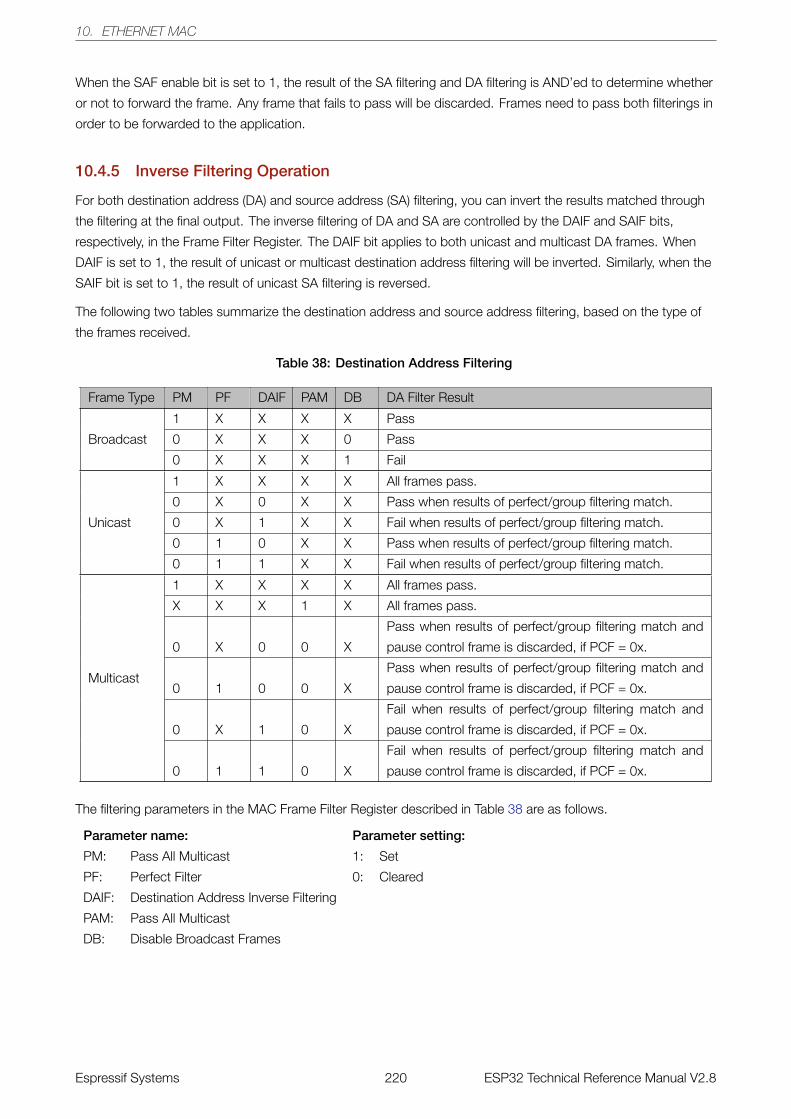
10. ETHERNET MAC
When the SAF enable bit is set to 1, the result of the SA filtering and DA filtering is AND’ed to determine whether
or not to forward the frame. Any frame that fails to pass will be discarded. Frames need to pass both filterings in
order to be forwarded to the application.
10.4.5 Inverse Filtering Operation
For both destination address (DA) and source address (SA) filtering, you can invert the results matched through
the filtering at the final output. The inverse filtering of DA and SA are controlled by the DAIF and SAIF bits,
respectively, in the Frame Filter Register. The DAIF bit applies to both unicast and multicast DA frames. When
DAIF is set to 1, the result of unicast or multicast destination address filtering will be inverted. Similarly, when the
SAIF bit is set to 1, the result of unicast SA filtering is reversed.
The following two tables summarize the destination address and source address filtering, based on the type of
the frames received.
Table 38: Destination Address Filtering
Frame Type PM PF DAIF PAM DB DA Filter Result
Broadcast
1 X X X X Pass
0 X X X 0 Pass
0 X X X 1 Fail
Unicast
1 X X X X All frames pass.
0 X 0 X X Pass when results of perfect/group filtering match.
0 X 1 X X Fail when results of perfect/group filtering match.
0 1 0 X X Pass when results of perfect/group filtering match.
0 1 1 X X Fail when results of perfect/group filtering match.
Multicast
1 X X X X All frames pass.
X X X 1 X All frames pass.
0 X 0 0 X
Pass when results of perfect/group filtering match and
pause control frame is discarded, if PCF = 0x.
0 1 0 0 X
Pass when results of perfect/group filtering match and
pause control frame is discarded, if PCF = 0x.
0 X 1 0 X
Fail when results of perfect/group filtering match and
pause control frame is discarded, if PCF = 0x.
0 1 1 0 X
Fail when results of perfect/group filtering match and
pause control frame is discarded, if PCF = 0x.
The filtering parameters in the MAC Frame Filter Register described in Table 38 are as follows.
Parameter name: Parameter setting:
PM: Pass All Multicast 1: Set
PF: Perfect Filter 0: Cleared
DAIF: Destination Address Inverse Filtering
PAM: Pass All Multicast
DB: Disable Broadcast Frames
Espressif Systems 220 ESP32 Technical Reference Manual V2.8
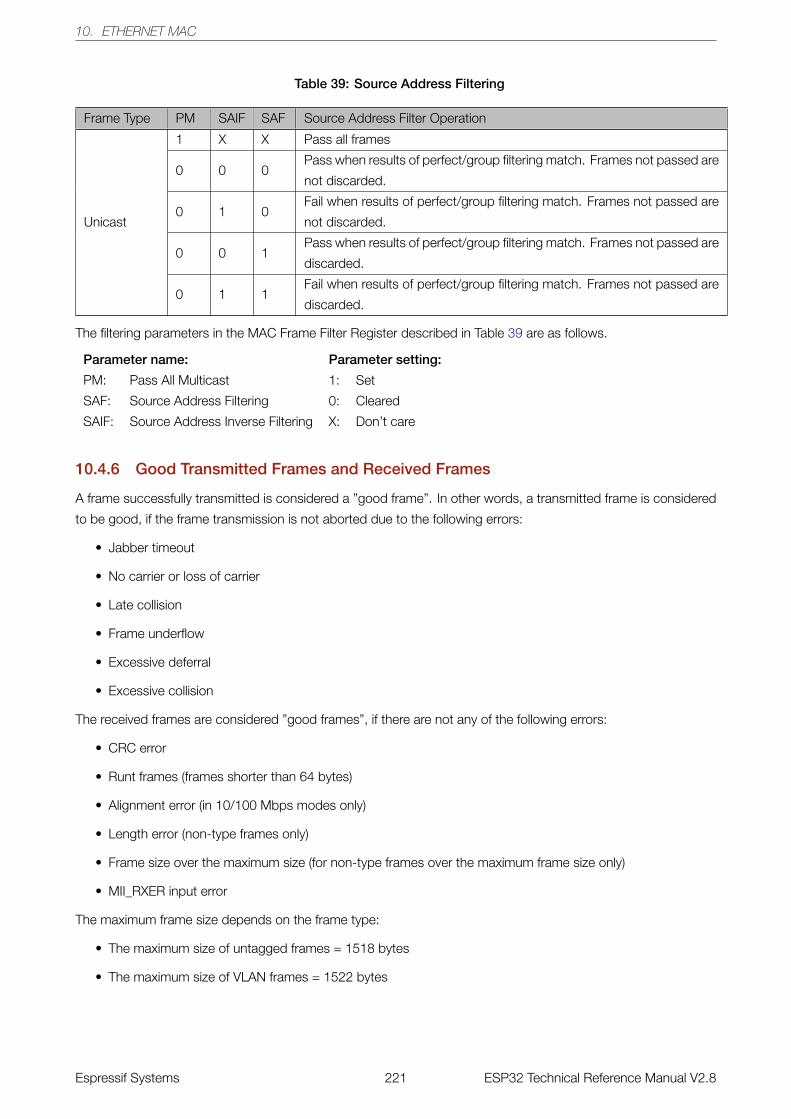
10. ETHERNET MAC
Table 39: Source Address Filtering
Frame Type PM SAIF SAF Source Address Filter Operation
Unicast
1 X X Pass all frames
0 0 0Pass when results of perfect/group filtering match. Frames not passed are
not discarded.
0 1 0Fail when results of perfect/group filtering match. Frames not passed are
not discarded.
0 0 1Pass when results of perfect/group filtering match. Frames not passed are
discarded.
0 1 1Fail when results of perfect/group filtering match. Frames not passed are
discarded.
The filtering parameters in the MAC Frame Filter Register described in Table 39 are as follows.
Parameter name: Parameter setting:
PM: Pass All Multicast 1: Set
SAF: Source Address Filtering 0: Cleared
SAIF: Source Address Inverse Filtering X: Don’t care
10.4.6 Good Transmitted Frames and Received Frames
A frame successfully transmitted is considered a ”good frame”. In other words, a transmitted frame is considered
to be good, if the frame transmission is not aborted due to the following errors:
• Jabber timeout
• No carrier or loss of carrier
• Late collision
• Frame underflow
• Excessive deferral
• Excessive collision
The received frames are considered ”good frames”, if there are not any of the following errors:
• CRC error
• Runt frames (frames shorter than 64 bytes)
• Alignment error (in 10/100 Mbps modes only)
• Length error (non-type frames only)
• Frame size over the maximum size (for non-type frames over the maximum frame size only)�
• MII_RXER input error
The maximum frame size depends on the frame type:
• The maximum size of untagged frames = 1518 bytes
• The maximum size of VLAN frames = 1522 bytes
Espressif Systems 221 ESP32 Technical Reference Manual V2.8
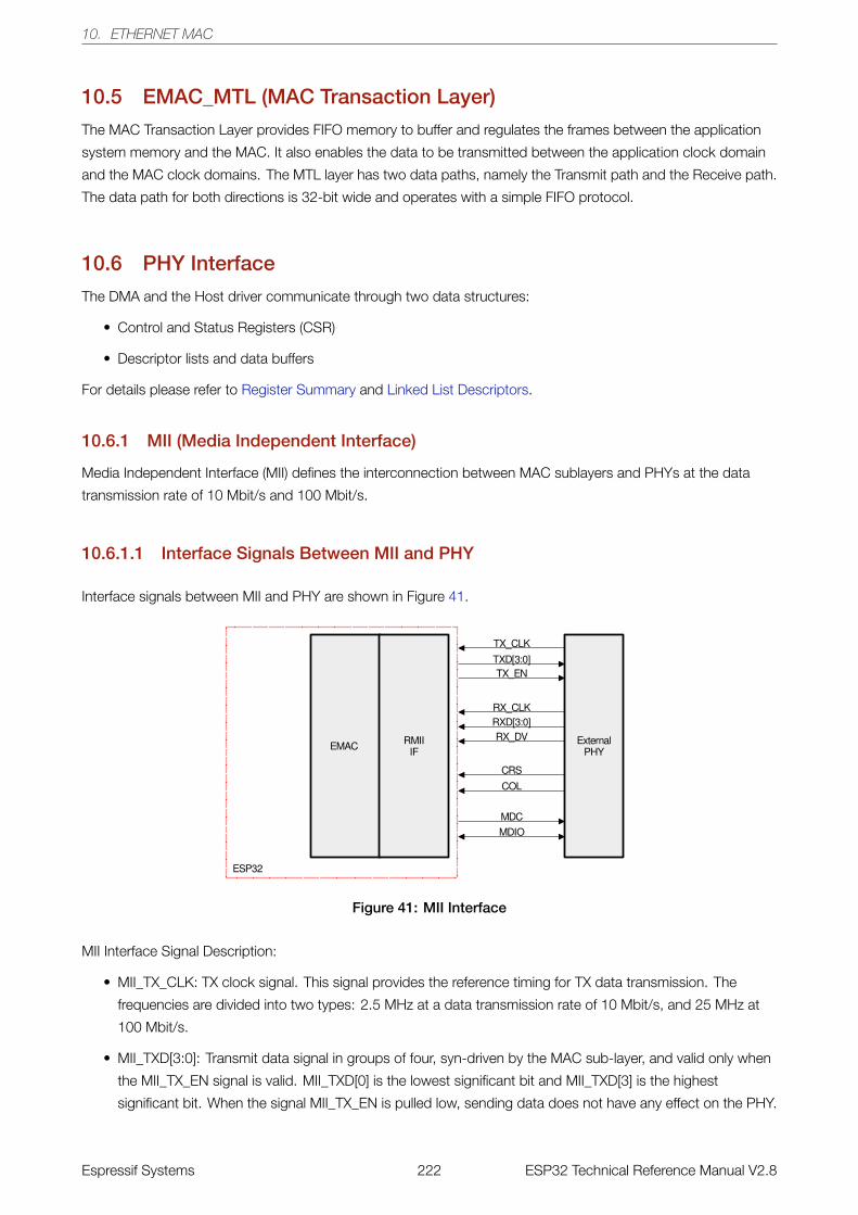
10. ETHERNET MAC
10.5 EMAC_MTL (MAC Transaction Layer)
The MAC Transaction Layer provides FIFO memory to buffer and regulates the frames between the application
system memory and the MAC. It also enables the data to be transmitted between the application clock domain
and the MAC clock domains. The MTL layer has two data paths, namely the Transmit path and the Receive path.
The data path for both directions is 32-bit wide and operates with a simple FIFO protocol.
10.6 PHY Interface
The DMA and the Host driver communicate through two data structures:
• Control and Status Registers (CSR)
• Descriptor lists and data buffers
For details please refer to Register Summary and Linked List Descriptors.
10.6.1 MII (Media Independent Interface)
Media Independent Interface (MII) defines the interconnection between MAC sublayers and PHYs at the data
transmission rate of 10 Mbit/s and 100 Mbit/s.
10.6.1.1 Interface Signals Between MII and PHY
Interface signals between MII and PHY are shown in Figure 41.
Figure 41: MII Interface
MII Interface Signal Description:
• MII_TX_CLK: TX clock signal. This signal provides the reference timing for TX data transmission. The
frequencies are divided into two types: 2.5 MHz at a data transmission rate of 10 Mbit/s, and 25 MHz at
100 Mbit/s.
• MII_TXD[3:0]: Transmit data signal in groups of four, syn-driven by the MAC sub-layer, and valid only when
the MII_TX_EN signal is valid. MII_TXD[0] is the lowest significant bit and MII_TXD[3] is the highest
significant bit. When the signal MII_TX_EN is pulled low, sending data does not have any effect on the PHY.
Espressif Systems 222 ESP32 Technical Reference Manual V2.8
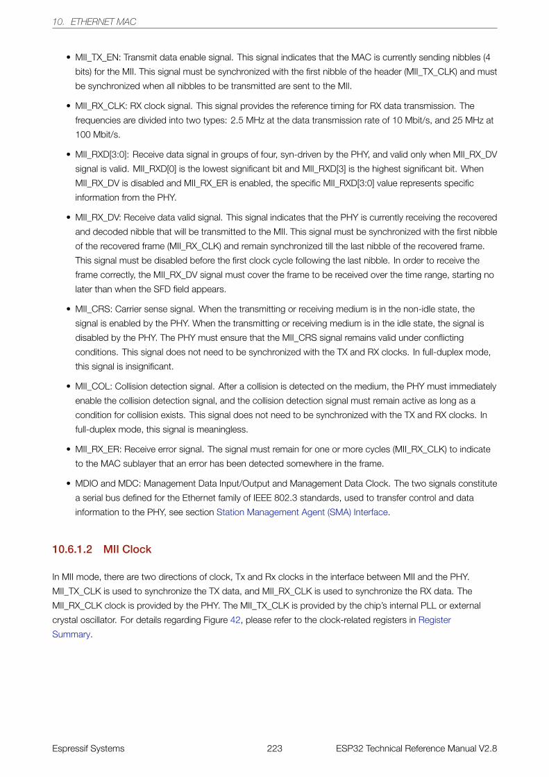
10. ETHERNET MAC
• MII_TX_EN: Transmit data enable signal. This signal indicates that the MAC is currently sending nibbles (4
bits) for the MII. This signal must be synchronized with the first nibble of the header (MII_TX_CLK) and must
be synchronized when all nibbles to be transmitted are sent to the MII.
• MII_RX_CLK: RX clock signal. This signal provides the reference timing for RX data transmission. The
frequencies are divided into two types: 2.5 MHz at the data transmission rate of 10 Mbit/s, and 25 MHz at
100 Mbit/s.
• MII_RXD[3:0]: Receive data signal in groups of four, syn-driven by the PHY, and valid only when MII_RX_DV
signal is valid. MII_RXD[0] is the lowest significant bit and MII_RXD[3] is the highest significant bit. When
MII_RX_DV is disabled and MII_RX_ER is enabled, the specific MII_RXD[3:0] value represents specific
information from the PHY.
• MII_RX_DV: Receive data valid signal. This signal indicates that the PHY is currently receiving the recovered
and decoded nibble that will be transmitted to the MII. This signal must be synchronized with the first nibble
of the recovered frame (MII_RX_CLK) and remain synchronized till the last nibble of the recovered frame.
This signal must be disabled before the first clock cycle following the last nibble. In order to receive the
frame correctly, the MII_RX_DV signal must cover the frame to be received over the time range, starting no
later than when the SFD field appears.
• MII_CRS: Carrier sense signal. When the transmitting or receiving medium is in the non-idle state, the
signal is enabled by the PHY. When the transmitting or receiving medium is in the idle state, the signal is
disabled by the PHY. The PHY must ensure that the MII_CRS signal remains valid under conflicting
conditions. This signal does not need to be synchronized with the TX and RX clocks. In full-duplex mode,
this signal is insignificant.
• MII_COL: Collision detection signal. After a collision is detected on the medium, the PHY must immediately
enable the collision detection signal, and the collision detection signal must remain active as long as a
condition for collision exists. This signal does not need to be synchronized with the TX and RX clocks. In
full-duplex mode, this signal is meaningless.
• MII_RX_ER: Receive error signal. The signal must remain for one or more cycles (MII_RX_CLK) to indicate
to the MAC sublayer that an error has been detected somewhere in the frame.
• MDIO and MDC: Management Data Input/Output and Management Data Clock. The two signals constitute
a serial bus defined for the Ethernet family of IEEE 802.3 standards, used to transfer control and data
information to the PHY, see section Station Management Agent (SMA) Interface.
10.6.1.2 MII Clock
In MII mode, there are two directions of clock, Tx and Rx clocks in the interface between MII and the PHY.
MII_TX_CLK is used to synchronize the TX data, and MII_RX_CLK is used to synchronize the RX data. The
MII_RX_CLK clock is provided by the PHY. The MII_TX_CLK is provided by the chip’s internal PLL or external
crystal oscillator. For details regarding Figure 42, please refer to the clock-related registers in Register
Summary.
Espressif Systems 223 ESP32 Technical Reference Manual V2.8
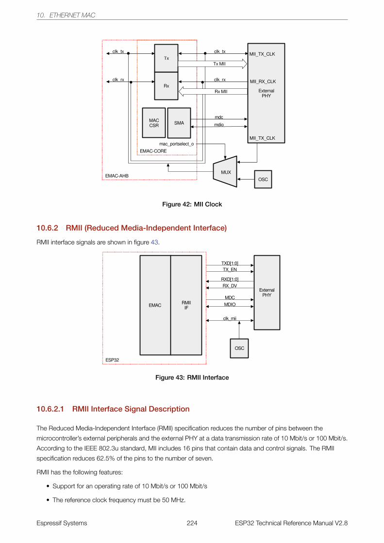
10. ETHERNET MAC
Figure 42: MII Clock
10.6.2 RMII (Reduced Media-Independent Interface)
RMII interface signals are shown in figure 43.
Figure 43: RMII Interface
10.6.2.1 RMII Interface Signal Description
The Reduced Media-Independent Interface (RMII) specification reduces the number of pins between the
microcontroller’s external peripherals and the external PHY at a data transmission rate of 10 Mbit/s or 100 Mbit/s.
According to the IEEE 802.3u standard, MII includes 16 pins that contain data and control signals. The RMII
specification reduces 62.5% of the pins to the number of seven.
RMII has the following features:
• Support for an operating rate of 10 Mbit/s or 100 Mbit/s
• The reference clock frequency must be 50 MHz.
Espressif Systems 224 ESP32 Technical Reference Manual V2.8
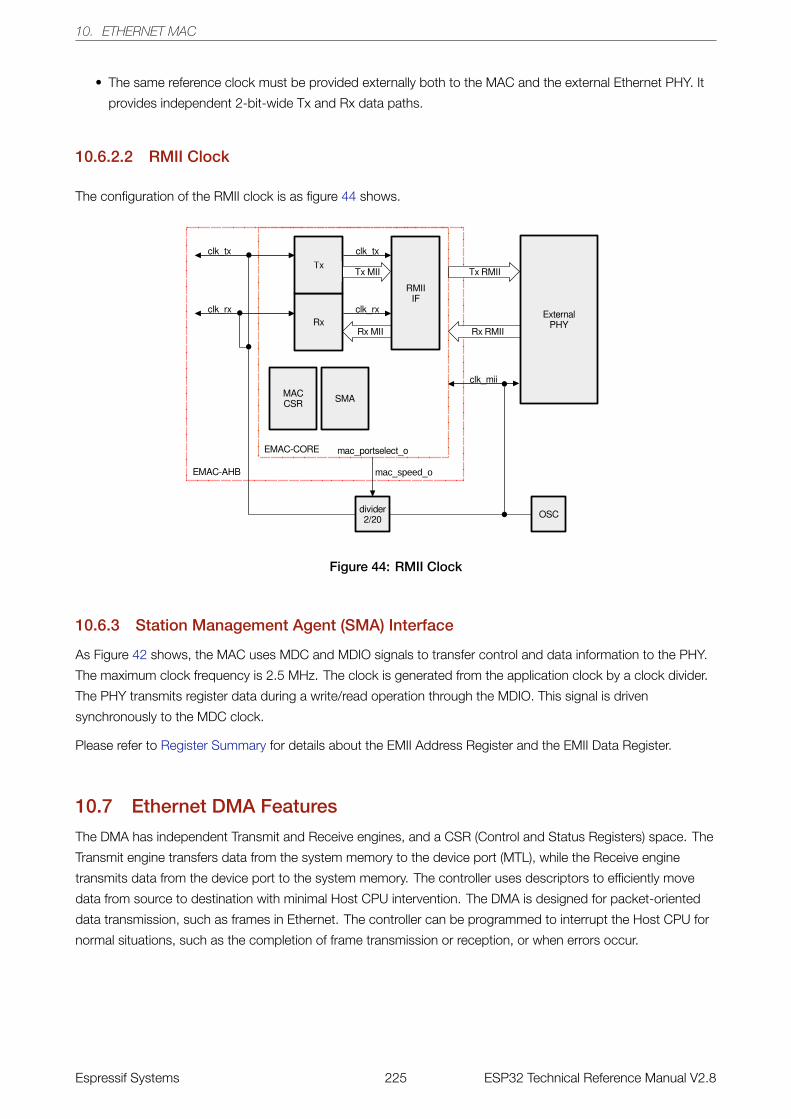
10. ETHERNET MAC
• The same reference clock must be provided externally both to the MAC and the external Ethernet PHY. It
provides independent 2-bit-wide Tx and Rx data paths.
10.6.2.2 RMII Clock
The configuration of the RMII clock is as figure 44 shows.
Figure 44: RMII Clock
10.6.3 Station Management Agent (SMA) Interface
As Figure 42 shows, the MAC uses MDC and MDIO signals to transfer control and data information to the PHY.
The maximum clock frequency is 2.5 MHz. The clock is generated from the application clock by a clock divider.
The PHY transmits register data during a write/read operation through the MDIO. This signal is driven
synchronously to the MDC clock.
Please refer to Register Summary for details about the EMII Address Register and the EMII Data Register.
10.7 Ethernet DMA Features
The DMA has independent Transmit and Receive engines, and a CSR (Control and Status Registers) space. The
Transmit engine transfers data from the system memory to the device port (MTL), while the Receive engine
transmits data from the device port to the system memory. The controller uses descriptors to efficiently move
data from source to destination with minimal Host CPU intervention. The DMA is designed for packet-oriented
data transmission, such as frames in Ethernet. The controller can be programmed to interrupt the Host CPU for
normal situations, such as the completion of frame transmission or reception, or when errors occur.
Espressif Systems 225 ESP32 Technical Reference Manual V2.8
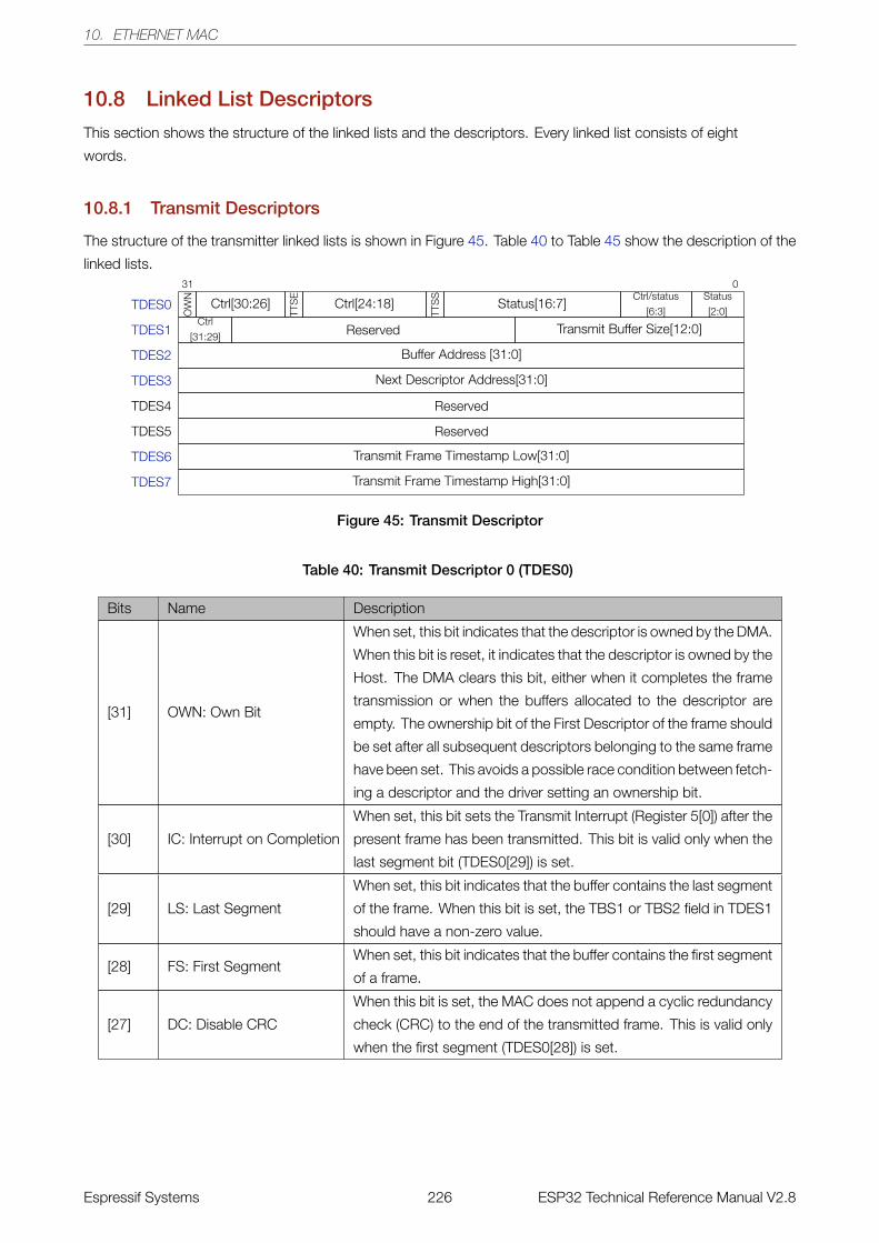
10. ETHERNET MAC
10.8 Linked List Descriptors
This section shows the structure of the linked lists and the descriptors. Every linked list consists of eight
words.
10.8.1 Transmit Descriptors
The structure of the transmitter linked lists is shown in Figure 45. Table 40 to Table 45 show the description of the
linked lists.031
OW
N
Ctrl[30:26]TT
SE
Ctrl[24:18]
TTS
S
Status[16:7]Ctrl/status
[6:3]
Status
[2:0]TDES0Ctrl
[31:29] Reserved Transmit Buffer Size[12:0]TDES1
Buffer Address [31:0]TDES2
Next Descriptor Address[31:0]TDES3
ReservedTDES4
ReservedTDES5
Transmit Frame Timestamp Low[31:0]TDES6
Transmit Frame Timestamp High[31:0]TDES7
Figure 45: Transmit Descriptor
Table 40: Transmit Descriptor 0 (TDES0)
Bits Name Description
[31] OWN: Own Bit
When set, this bit indicates that the descriptor is owned by the DMA.
When this bit is reset, it indicates that the descriptor is owned by the
Host. The DMA clears this bit, either when it completes the frame
transmission or when the buffers allocated to the descriptor are
empty. The ownership bit of the First Descriptor of the frame should
be set after all subsequent descriptors belonging to the same frame
have been set. This avoids a possible race condition between fetch-
ing a descriptor and the driver setting an ownership bit.
[30] IC: Interrupt on Completion
When set, this bit sets the Transmit Interrupt (Register 5[0]) after the
present frame has been transmitted. This bit is valid only when the
last segment bit (TDES0[29]) is set.
[29] LS: Last Segment
When set, this bit indicates that the buffer contains the last segment
of the frame. When this bit is set, the TBS1 or TBS2 field in TDES1
should have a non-zero value.
[28] FS: First SegmentWhen set, this bit indicates that the buffer contains the first segment
of a frame.
[27] DC: Disable CRC
When this bit is set, the MAC does not append a cyclic redundancy
check (CRC) to the end of the transmitted frame. This is valid only
when the first segment (TDES0[28]) is set.
Espressif Systems 226 ESP32 Technical Reference Manual V2.8
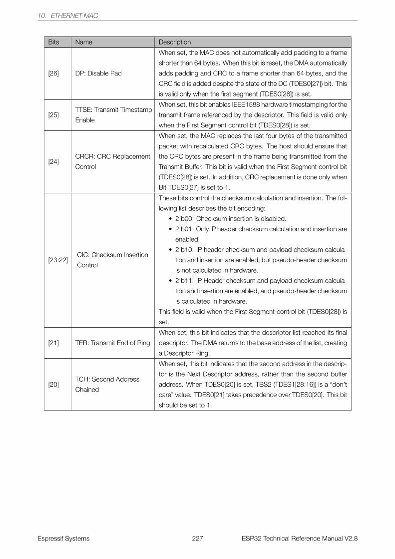
10. ETHERNET MAC
Bits Name Description
[26] DP: Disable Pad
When set, the MAC does not automatically add padding to a frame
shorter than 64 bytes. When this bit is reset, the DMA automatically
adds padding and CRC to a frame shorter than 64 bytes, and the
CRC field is added despite the state of the DC (TDES0[27]) bit. This
is valid only when the first segment (TDES0[28]) is set.
[25]TTSE: Transmit Timestamp
Enable
When set, this bit enables IEEE1588 hardware timestamping for the
transmit frame referenced by the descriptor. This field is valid only
when the First Segment control bit (TDES0[28]) is set.
[24]CRCR: CRC Replacement
Control
When set, the MAC replaces the last four bytes of the transmitted
packet with recalculated CRC bytes. The host should ensure that
the CRC bytes are present in the frame being transmitted from the
Transmit Buffer. This bit is valid when the First Segment control bit
(TDES0[28]) is set. In addition, CRC replacement is done only when
Bit TDES0[27] is set to 1.
[23:22]CIC: Checksum Insertion
Control
These bits control the checksum calculation and insertion. The fol-
lowing list describes the bit encoding:
• 2’b00: Checksum insertion is disabled.
• 2’b01: Only IP header checksum calculation and insertion are
enabled.
• 2’b10: IP header checksum and payload checksum calcula-
tion and insertion are enabled, but pseudo-header checksum
is not calculated in hardware.
• 2’b11: IP Header checksum and payload checksum calcula-
tion and insertion are enabled, and pseudo-header checksum
is calculated in hardware.
This field is valid when the First Segment control bit (TDES0[28]) is
set.
[21] TER: Transmit End of Ring
When set, this bit indicates that the descriptor list reached its final
descriptor. The DMA returns to the base address of the list, creating
a Descriptor Ring.
[20]TCH: Second Address
Chained
When set, this bit indicates that the second address in the descrip-
tor is the Next Descriptor address, rather than the second buffer
address. When TDES0[20] is set, TBS2 (TDES1[28:16]) is a “don’t
care” value. TDES0[21] takes precedence over TDES0[20]. This bit
should be set to 1.
Espressif Systems 227 ESP32 Technical Reference Manual V2.8
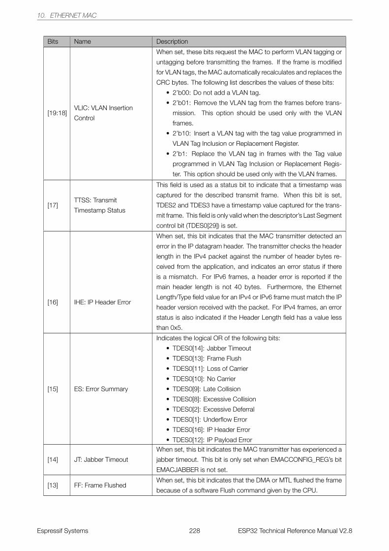
10. ETHERNET MAC
Bits Name Description
[19:18]VLIC: VLAN Insertion
Control
When set, these bits request the MAC to perform VLAN tagging or
untagging before transmitting the frames. If the frame is modified
for VLAN tags, the MAC automatically recalculates and replaces the
CRC bytes. The following list describes the values of these bits:
• 2’b00: Do not add a VLAN tag.
• 2’b01: Remove the VLAN tag from the frames before trans-
mission. This option should be used only with the VLAN
frames.
• 2’b10: Insert a VLAN tag with the tag value programmed in
VLAN Tag Inclusion or Replacement Register.
• 2’b1: Replace the VLAN tag in frames with the Tag value
programmed in VLAN Tag Inclusion or Replacement Regis-
ter. This option should be used only with the VLAN frames.
[17]TTSS: Transmit
Timestamp Status
This field is used as a status bit to indicate that a timestamp was
captured for the described transmit frame. When this bit is set,
TDES2 and TDES3 have a timestamp value captured for the trans-
mit frame. This field is only valid when the descriptor’s Last Segment
control bit (TDES0[29]) is set.
[16] IHE: IP Header Error
When set, this bit indicates that the MAC transmitter detected an
error in the IP datagram header. The transmitter checks the header
length in the IPv4 packet against the number of header bytes re-
ceived from the application, and indicates an error status if there
is a mismatch. For IPv6 frames, a header error is reported if the
main header length is not 40 bytes. Furthermore, the Ethernet
Length/Type field value for an IPv4 or IPv6 frame must match the IP
header version received with the packet. For IPv4 frames, an error
status is also indicated if the Header Length field has a value less
than 0x5.
[15] ES: Error Summary
Indicates the logical OR of the following bits:
• TDES0[14]: Jabber Timeout
• TDES0[13]: Frame Flush
• TDES0[11]: Loss of Carrier
• TDES0[10]: No Carrier
• TDES0[9]: Late Collision
• TDES0[8]: Excessive Collision
• TDES0[2]: Excessive Deferral
• TDES0[1]: Underflow Error
• TDES0[16]: IP Header Error
• TDES0[12]: IP Payload Error
[14] JT: Jabber Timeout
When set, this bit indicates the MAC transmitter has experienced a
jabber timeout. This bit is only set when EMACCONFIG_REG’s bit
EMACJABBER is not set.
[13] FF: Frame FlushedWhen set, this bit indicates that the DMA or MTL flushed the frame
because of a software Flush command given by the CPU.
Espressif Systems 228 ESP32 Technical Reference Manual V2.8
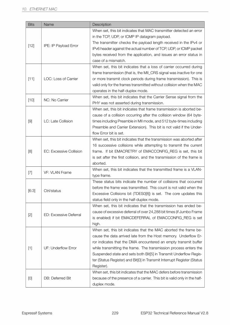
10. ETHERNET MAC
Bits Name Description
[12] IPE: IP Payload Error
When set, this bit indicates that MAC transmitter detected an error
in the TCP, UDP, or ICMP IP datagram payload.
The transmitter checks the payload length received in the IPv4 or
IPv6 header against the actual number of TCP, UDP, or ICMP packet
bytes received from the application, and issues an error status in
case of a mismatch.
[11] LOC: Loss of Carrier
When set, this bit indicates that a loss of carrier occurred during
frame transmission (that is, the MII_CRS signal was inactive for one
or more transmit clock periods during frame transmission). This is
valid only for the frames transmitted without collision when the MAC
operates in the half-duplex mode.
[10] NC: No CarrierWhen set, this bit indicates that the Carrier Sense signal from the
PHY was not asserted during transmission.
[9] LC: Late Collision
When set, this bit indicates that frame transmission is aborted be-
cause of a collision occurring after the collision window (64 byte-
times including Preamble in MII mode, and 512 byte-times including
Preamble and Carrier Extension). This bit is not valid if the Under-
flow Error bit is set.
[8] EC: Excessive Collision
When set, this bit indicates that the transmission was aborted after
16 successive collisions while attempting to transmit the current
frame. If bit EMACRETRY of EMACCONFIG_REG is set, this bit
is set after the first collision, and the transmission of the frame is
aborted.
[7] VF: VLAN FrameWhen set, this bit indicates that the transmitted frame is a VLAN-
type frame.
[6:3] Ctrl/status
These status bits indicate the number of collisions that occurred
before the frame was transmitted. This count is not valid when the
Excessive Collisions bit (TDES0[8]) is set. The core updates this
status field only in the half-duplex mode.
[2] ED: Excessive Deferral
When set, this bit indicates that the transmission has ended be-
cause of excessive deferral of over 24,288 bit times (if Jumbo Frame
is enabled) if bit EMACDEFERRAL of EMACCONFIG_REG is set
high.
[1] UF: Underflow Error
When set, this bit indicates that the MAC aborted the frame be-
cause the data arrived late from the Host memory. Underflow Er-
ror indicates that the DMA encountered an empty transmit buffer
while transmitting the frame. The transmission process enters the
Suspended state and sets both Bit[5] in Transmit Underflow Regis-
ter (Status Register) and Bit[0] in Transmit Interrupt Register (Status
Register).
[0] DB: Deferred Bit
When set, this bit indicates that the MAC defers before transmission
because of the presence of a carrier. This bit is valid only in the half-
duplex mode.
Espressif Systems 229 ESP32 Technical Reference Manual V2.8
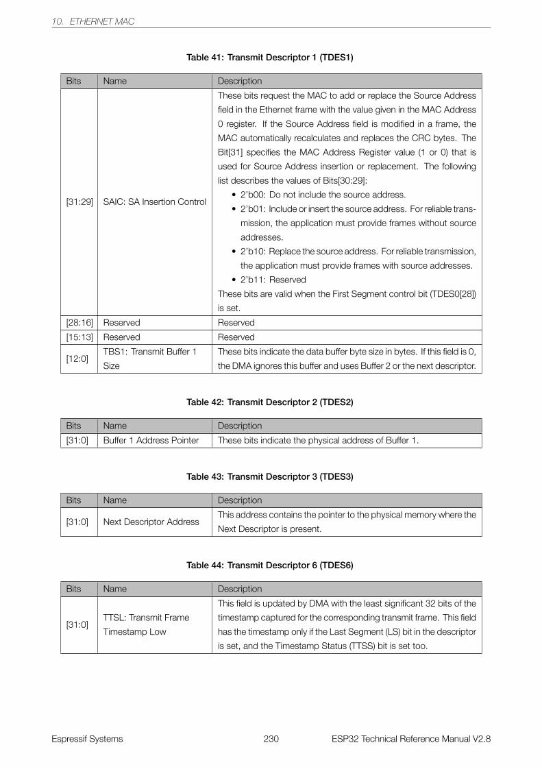
10. ETHERNET MAC
Table 41: Transmit Descriptor 1 (TDES1)
Bits Name Description
[31:29] SAIC: SA Insertion Control
These bits request the MAC to add or replace the Source Address
field in the Ethernet frame with the value given in the MAC Address
0 register. If the Source Address field is modified in a frame, the
MAC automatically recalculates and replaces the CRC bytes. The
Bit[31] specifies the MAC Address Register value (1 or 0) that is
used for Source Address insertion or replacement. The following
list describes the values of Bits[30:29]:
• 2’b00: Do not include the source address.
• 2’b01: Include or insert the source address. For reliable trans-
mission, the application must provide frames without source
addresses.
• 2’b10: Replace the source address. For reliable transmission,
the application must provide frames with source addresses.
• 2’b11: Reserved
These bits are valid when the First Segment control bit (TDES0[28])
is set.
[28:16] Reserved Reserved
[15:13] Reserved Reserved
[12:0]TBS1: Transmit Buffer 1
Size
These bits indicate the data buffer byte size in bytes. If this field is 0,
the DMA ignores this buffer and uses Buffer 2 or the next descriptor.
Table 42: Transmit Descriptor 2 (TDES2)
Bits Name Description
[31:0] Buffer 1 Address Pointer These bits indicate the physical address of Buffer 1.
Table 43: Transmit Descriptor 3 (TDES3)
Bits Name Description
[31:0] Next Descriptor AddressThis address contains the pointer to the physical memory where the
Next Descriptor is present.
Table 44: Transmit Descriptor 6 (TDES6)
Bits Name Description
[31:0]TTSL: Transmit Frame
Timestamp Low
This field is updated by DMA with the least significant 32 bits of the
timestamp captured for the corresponding transmit frame. This field
has the timestamp only if the Last Segment (LS) bit in the descriptor
is set, and the Timestamp Status (TTSS) bit is set too.
Espressif Systems 230 ESP32 Technical Reference Manual V2.8
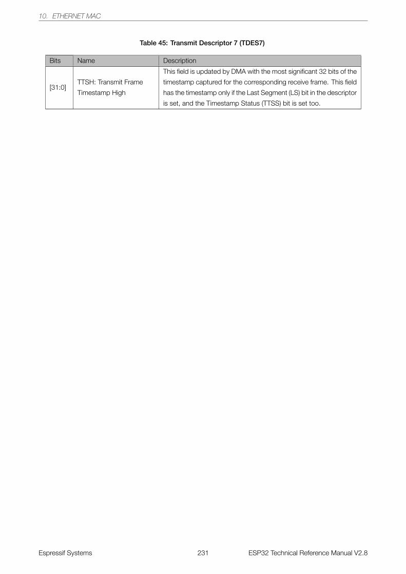
10. ETHERNET MAC
Table 45: Transmit Descriptor 7 (TDES7)
Bits Name Description
[31:0]TTSH: Transmit Frame
Timestamp High
This field is updated by DMA with the most significant 32 bits of the
timestamp captured for the corresponding receive frame. This field
has the timestamp only if the Last Segment (LS) bit in the descriptor
is set, and the Timestamp Status (TTSS) bit is set too.
Espressif Systems 231 ESP32 Technical Reference Manual V2.8
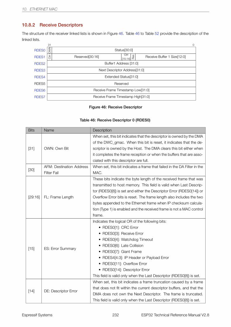
10. ETHERNET MAC
10.8.2 Receive Descriptors
The structure of the receiver linked lists is shown in Figure 46. Table 46 to Table 52 provide the description of the
linked lists.031
OW
NStatus[30:0]RDES0
Ctr
l
Reserved[30:16]Ctrl
[15:14] Res Receive Buffer 1 Size[12:0]RDES1
Buffer1 Address [31:0]RDES2
Next Descriptor Address[31:0]RDES3
Extended Status[31:0]RDES4
ReservedRDES5
Receive Frame Timestamp Low[31:0]RDES6
Receive Frame Timestamp High[31:0]RDES7
Figure 46: Receive Descriptor
Table 46: Receive Descriptor 0 (RDES0)
Bits Name Description
[31] OWN: Own Bit
When set, this bit indicates that the descriptor is owned by the DMA
of the DWC_gmac. When this bit is reset, it indicates that the de-
scriptor is owned by the Host. The DMA clears this bit either when
it completes the frame reception or when the buffers that are asso-
ciated with this descriptor are full.
[30]AFM: Destination Address
Filter Fail
When set, this bit indicates a frame that failed in the DA Filter in the
MAC.
[29:16] FL: Frame Length
These bits indicate the byte length of the received frame that was
transmitted to host memory. This field is valid when Last Descrip-
tor (RDES0[8]) is set and either the Descriptor Error (RDES0[14]) or
Overflow Error bits is reset. The frame length also includes the two
bytes appended to the Ethernet frame when IP checksum calcula-
tion (Type 1) is enabled and the received frame is not a MAC control
frame.
[15] ES: Error Summary
Indicates the logical OR of the following bits:
• RDES0[1]: CRC Error
• RDES0[3]: Receive Error
• RDES0[4]: Watchdog Timeout
• RDES0[6]: Late Collision
• RDES0[7]: Giant Frame
• RDES4[4:3]: IP Header or Payload Error
• RDES0[11]: Overflow Error
• RDES0[14]: Descriptor Error
This field is valid only when the Last Descriptor (RDES0[8]) is set.
[14] DE: Descriptor Error
When set, this bit indicates a frame truncation caused by a frame
that does not fit within the current descriptor buffers, and that the
DMA does not own the Next Descriptor. The frame is truncated.
This field is valid only when the Last Descriptor (RDES0[8]) is set.
Espressif Systems 232 ESP32 Technical Reference Manual V2.8
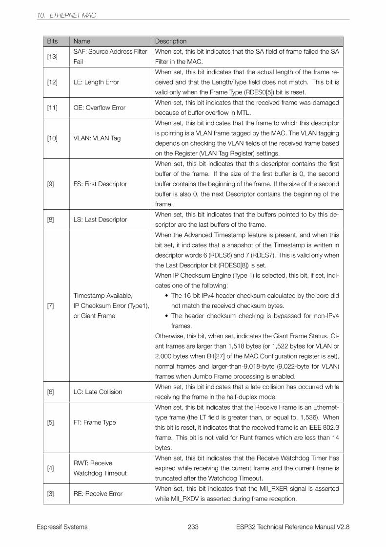
10. ETHERNET MAC
Bits Name Description
[13]SAF: Source Address Filter
Fail
When set, this bit indicates that the SA field of frame failed the SA
Filter in the MAC.
[12] LE: Length Error
When set, this bit indicates that the actual length of the frame re-
ceived and that the Length/Type field does not match. This bit is
valid only when the Frame Type (RDES0[5]) bit is reset.
[11] OE: Overflow ErrorWhen set, this bit indicates that the received frame was damaged
because of buffer overflow in MTL.
[10] VLAN: VLAN Tag
When set, this bit indicates that the frame to which this descriptor
is pointing is a VLAN frame tagged by the MAC. The VLAN tagging
depends on checking the VLAN fields of the received frame based
on the Register (VLAN Tag Register) settings.
[9] FS: First Descriptor
When set, this bit indicates that this descriptor contains the first
buffer of the frame. If the size of the first buffer is 0, the second
buffer contains the beginning of the frame. If the size of the second
buffer is also 0, the next Descriptor contains the beginning of the
frame.
[8] LS: Last DescriptorWhen set, this bit indicates that the buffers pointed to by this de-
scriptor are the last buffers of the frame.
[7]
Timestamp Available,
IP Checksum Error (Type1),
or Giant Frame
When the Advanced Timestamp feature is present, and when this
bit set, it indicates that a snapshot of the Timestamp is written in
descriptor words 6 (RDES6) and 7 (RDES7). This is valid only when
the Last Descriptor bit (RDES0[8]) is set.
When IP Checksum Engine (Type 1) is selected, this bit, if set, indi-
cates one of the following:
• The 16-bit IPv4 header checksum calculated by the core did
not match the received checksum bytes.
• The header checksum checking is bypassed for non-IPv4
frames.
Otherwise, this bit, when set, indicates the Giant Frame Status. Gi-
ant frames are larger than 1,518 bytes (or 1,522 bytes for VLAN or
2,000 bytes when Bit[27] of the MAC Configuration register is set),
normal frames and larger-than-9,018-byte (9,022-byte for VLAN)
frames when Jumbo Frame processing is enabled.
[6] LC: Late CollisionWhen set, this bit indicates that a late collision has occurred while
receiving the frame in the half-duplex mode.
[5] FT: Frame Type
When set, this bit indicates that the Receive Frame is an Ethernet-
type frame (the LT field is greater than, or equal to, 1,536). When
this bit is reset, it indicates that the received frame is an IEEE 802.3
frame. This bit is not valid for Runt frames which are less than 14
bytes.
[4]RWT: Receive
Watchdog Timeout
When set, this bit indicates that the Receive Watchdog Timer has
expired while receiving the current frame and the current frame is
truncated after the Watchdog Timeout.
[3] RE: Receive ErrorWhen set, this bit indicates that the MII_RXER signal is asserted
while MII_RXDV is asserted during frame reception.
Espressif Systems 233 ESP32 Technical Reference Manual V2.8
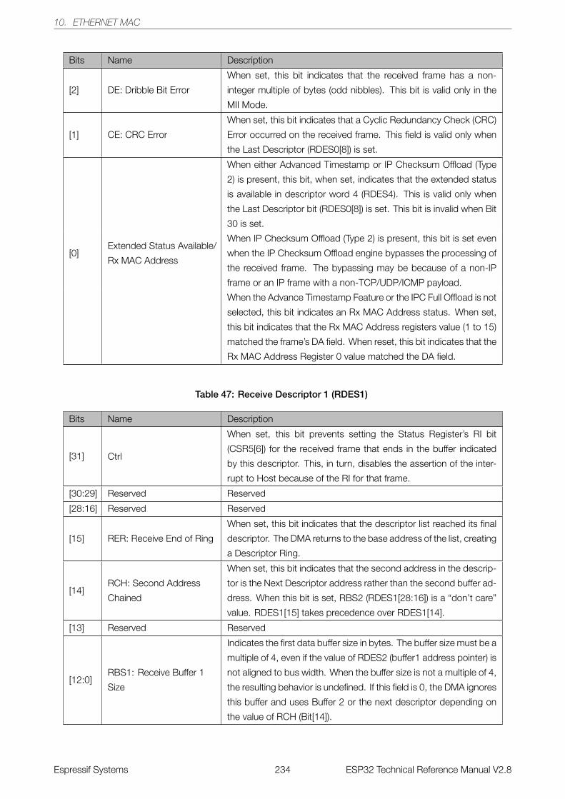
10. ETHERNET MAC
Bits Name Description
[2] DE: Dribble Bit Error
When set, this bit indicates that the received frame has a non-
integer multiple of bytes (odd nibbles). This bit is valid only in the
MII Mode.
[1] CE: CRC Error
When set, this bit indicates that a Cyclic Redundancy Check (CRC)
Error occurred on the received frame. This field is valid only when
the Last Descriptor (RDES0[8]) is set.
[0]Extended Status Available/
Rx MAC Address
When either Advanced Timestamp or IP Checksum Offload (Type
2) is present, this bit, when set, indicates that the extended status
is available in descriptor word 4 (RDES4). This is valid only when
the Last Descriptor bit (RDES0[8]) is set. This bit is invalid when Bit
30 is set.
When IP Checksum Offload (Type 2) is present, this bit is set even
when the IP Checksum Offload engine bypasses the processing of
the received frame. The bypassing may be because of a non-IP
frame or an IP frame with a non-TCP/UDP/ICMP payload.
When the Advance Timestamp Feature or the IPC Full Offload is not
selected, this bit indicates an Rx MAC Address status. When set,
this bit indicates that the Rx MAC Address registers value (1 to 15)
matched the frame’s DA field. When reset, this bit indicates that the
Rx MAC Address Register 0 value matched the DA field.
Table 47: Receive Descriptor 1 (RDES1)
Bits Name Description
[31] Ctrl
When set, this bit prevents setting the Status Register’s RI bit
(CSR5[6]) for the received frame that ends in the buffer indicated
by this descriptor. This, in turn, disables the assertion of the inter-
rupt to Host because of the RI for that frame.
[30:29] Reserved Reserved
[28:16] Reserved Reserved
[15] RER: Receive End of Ring
When set, this bit indicates that the descriptor list reached its final
descriptor. The DMA returns to the base address of the list, creating
a Descriptor Ring.
[14]RCH: Second Address
Chained
When set, this bit indicates that the second address in the descrip-
tor is the Next Descriptor address rather than the second buffer ad-
dress. When this bit is set, RBS2 (RDES1[28:16]) is a “don’t care”
value. RDES1[15] takes precedence over RDES1[14].
[13] Reserved Reserved
[12:0]RBS1: Receive Buffer 1
Size
Indicates the first data buffer size in bytes. The buffer size must be a
multiple of 4, even if the value of RDES2 (buffer1 address pointer) is
not aligned to bus width. When the buffer size is not a multiple of 4,
the resulting behavior is undefined. If this field is 0, the DMA ignores
this buffer and uses Buffer 2 or the next descriptor depending on
the value of RCH (Bit[14]).
Espressif Systems 234 ESP32 Technical Reference Manual V2.8
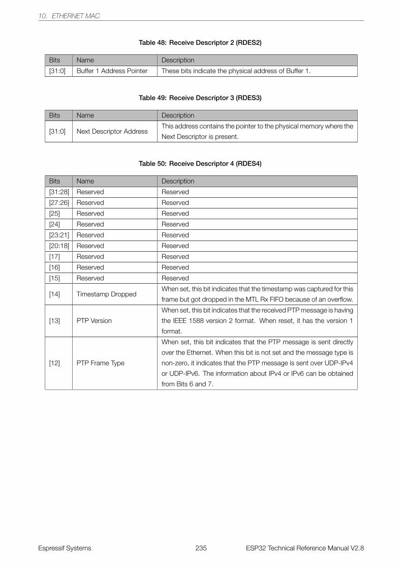
10. ETHERNET MAC
Table 48: Receive Descriptor 2 (RDES2)
Bits Name Description
[31:0] Buffer 1 Address Pointer These bits indicate the physical address of Buffer 1.
Table 49: Receive Descriptor 3 (RDES3)
Bits Name Description
[31:0] Next Descriptor AddressThis address contains the pointer to the physical memory where the
Next Descriptor is present.
Table 50: Receive Descriptor 4 (RDES4)
Bits Name Description
[31:28] Reserved Reserved
[27:26] Reserved Reserved
[25] Reserved Reserved
[24] Reserved Reserved
[23:21] Reserved Reserved
[20:18] Reserved Reserved
[17] Reserved Reserved
[16] Reserved Reserved
[15] Reserved Reserved
[14] Timestamp DroppedWhen set, this bit indicates that the timestamp was captured for this
frame but got dropped in the MTL Rx FIFO because of an overflow.
[13] PTP Version
When set, this bit indicates that the received PTP message is having
the IEEE 1588 version 2 format. When reset, it has the version 1
format.
[12] PTP Frame Type
When set, this bit indicates that the PTP message is sent directly
over the Ethernet. When this bit is not set and the message type is
non-zero, it indicates that the PTP message is sent over UDP-IPv4
or UDP-IPv6. The information about IPv4 or IPv6 can be obtained
from Bits 6 and 7.
Espressif Systems 235 ESP32 Technical Reference Manual V2.8
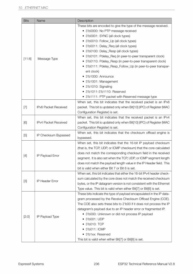
10. ETHERNET MAC
Bits Name Description
[11:8] Message Type
These bits are encoded to give the type of the message received.
• 3’b0000: No PTP message received
• 3’b0001: SYNC (all clock types)
• 3’b0010: Follow_Up (all clock types)
• 3’b0011: Delay_Req (all clock types)
• 3’b0100: Delay_Resp (all clock types)
• 3’b0101: Pdelay_Req (in peer-to-peer transparent clock)
• 3’b0110: Pdelay_Resp (in peer-to-peer transparent clock)
• 3’b0111: Pdelay_Resp_Follow_Up (in peer-to-peer transpar-
ent clock)
• 3’b1000: Announce
• 3’b1001: Management
• 3’b1010: Signaling
• 3’b1011-3’b1110: Reserved
• 3’b1111: PTP packet with Reserved message type
[7] IPv6 Packet Received
When set, this bit indicates that the received packet is an IPv6
packet. This bit is updated only when Bit[10] (IPC) of Register (MAC
Configuration Register) is set.
[6] IPv4 Packet Received
When set, this bit indicates that the received packet is an IPv4
packet. This bit is updated only when Bit[10] (IPC) of Register (MAC
Configuration Register) is set.
[5] IP Checksum BypassedWhen set, this bit indicates that the checksum offload engine is
bypassed.
[4] IP Payload Error
When set, this bit indicates that the 16-bit IP payload checksum
(that is, the TCP, UDP, or ICMP checksum) that the core calculated
does not match the corresponding checksum field in the received
segment. It is also set when the TCP, UDP, or ICMP segment length
does not match the payload length value in the IP Header field. This
bit is valid when either Bit 7 or Bit 6 is set.
[3] IP Header Error
When set, this bit indicates that either the 16-bit IPv4 header check-
sum calculated by the core does not match the received checksum
bytes, or the IP datagram version is not consistent with the Ethernet
Type value. This bit is valid when either Bit[7] or Bit[6] is set.
[2:0] IP Payload Type
These bits indicate the type of payload encapsulated in the IP data-
gram processed by the Receive Checksum Offload Engine (COE).
The COE also sets these bits to 2’b00 if it does not process the IP
datagram’s payload due to an IP header error or fragmented IP.
• 3’b000: Unknown or did not process IP payload
• 3’b001: UDP
• 3’b010: TCP
• 3’b011: ICMP
• 3’b1xx: Reserved
This bit is valid when either Bit[7] or Bit[6] is set.
Espressif Systems 236 ESP32 Technical Reference Manual V2.8
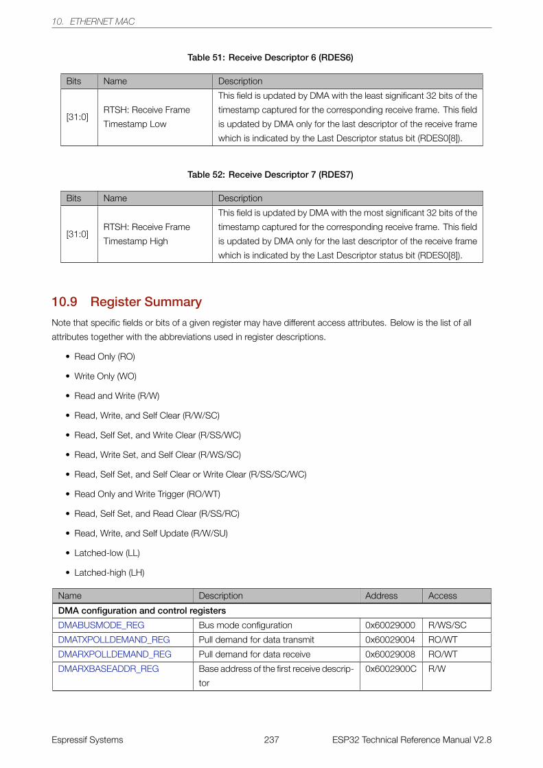
10. ETHERNET MAC
Table 51: Receive Descriptor 6 (RDES6)
Bits Name Description
[31:0]RTSH: Receive Frame
Timestamp Low
This field is updated by DMA with the least significant 32 bits of the
timestamp captured for the corresponding receive frame. This field
is updated by DMA only for the last descriptor of the receive frame
which is indicated by the Last Descriptor status bit (RDES0[8]).
Table 52: Receive Descriptor 7 (RDES7)
Bits Name Description
[31:0]RTSH: Receive Frame
Timestamp High
This field is updated by DMA with the most significant 32 bits of the
timestamp captured for the corresponding receive frame. This field
is updated by DMA only for the last descriptor of the receive frame
which is indicated by the Last Descriptor status bit (RDES0[8]).
10.9 Register Summary
Note that specific fields or bits of a given register may have different access attributes. Below is the list of all
attributes together with the abbreviations used in register descriptions.
• Read Only (RO)
• Write Only (WO)
• Read and Write (R/W)
• Read, Write, and Self Clear (R/W/SC)
• Read, Self Set, and Write Clear (R/SS/WC)
• Read, Write Set, and Self Clear (R/WS/SC)
• Read, Self Set, and Self Clear or Write Clear (R/SS/SC/WC)
• Read Only and Write Trigger (RO/WT)
• Read, Self Set, and Read Clear (R/SS/RC)
• Read, Write, and Self Update (R/W/SU)
• Latched-low (LL)
• Latched-high (LH)
Name Description Address Access
DMA configuration and control registers
DMABUSMODE_REG Bus mode configuration 0x60029000 R/WS/SC
DMATXPOLLDEMAND_REG Pull demand for data transmit 0x60029004 RO/WT
DMARXPOLLDEMAND_REG Pull demand for data receive 0x60029008 RO/WT
DMARXBASEADDR_REG Base address of the first receive descrip-
tor
0x6002900C R/W
Espressif Systems 237 ESP32 Technical Reference Manual V2.8
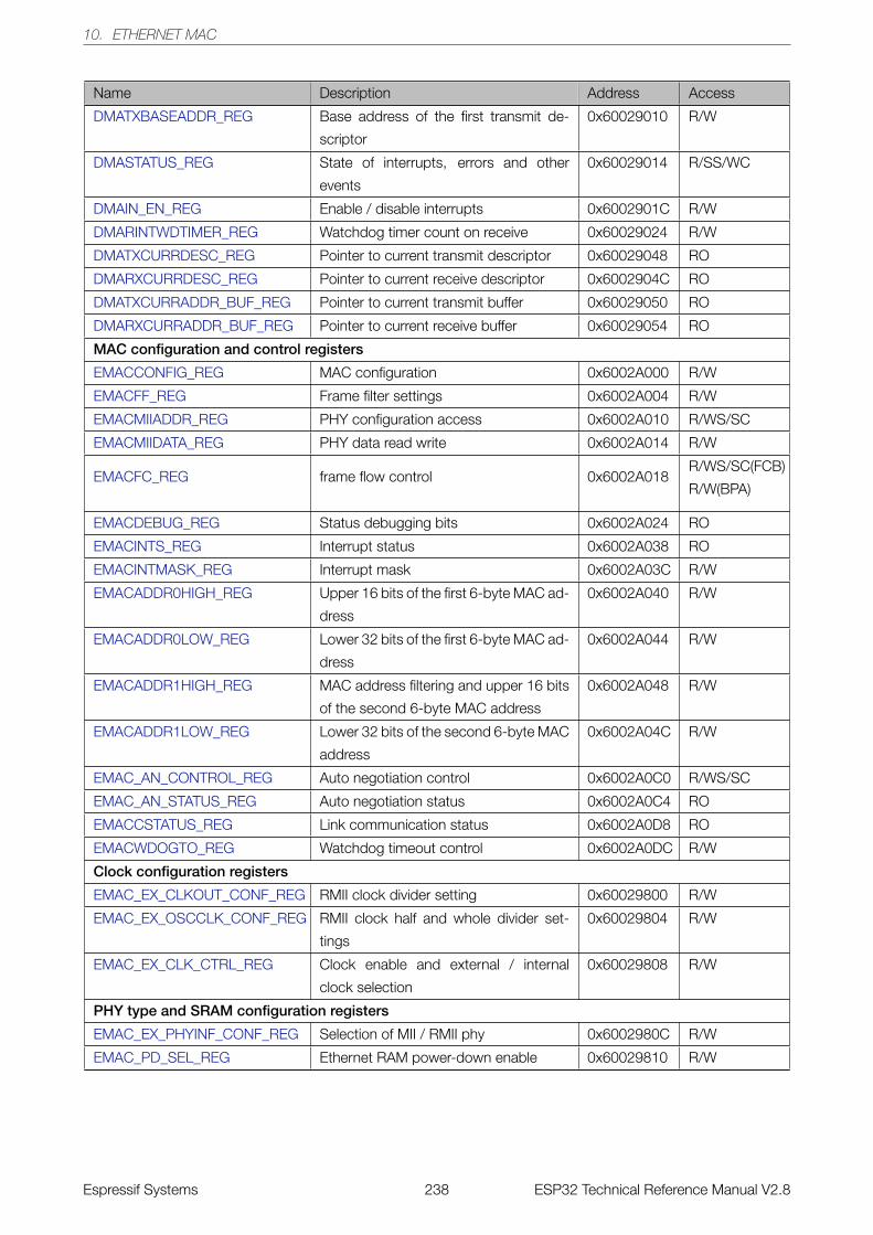
10. ETHERNET MAC
Name Description Address Access
DMATXBASEADDR_REG Base address of the first transmit de-
scriptor
0x60029010 R/W
DMASTATUS_REG State of interrupts, errors and other
events
0x60029014 R/SS/WC
DMAIN_EN_REG Enable / disable interrupts 0x6002901C R/W
DMARINTWDTIMER_REG Watchdog timer count on receive 0x60029024 R/W
DMATXCURRDESC_REG Pointer to current transmit descriptor 0x60029048 RO
DMARXCURRDESC_REG Pointer to current receive descriptor 0x6002904C RO
DMATXCURRADDR_BUF_REG Pointer to current transmit buffer 0x60029050 RO
DMARXCURRADDR_BUF_REG Pointer to current receive buffer 0x60029054 RO
MAC configuration and control registers
EMACCONFIG_REG MAC configuration 0x6002A000 R/W
EMACFF_REG Frame filter settings 0x6002A004 R/W
EMACMIIADDR_REG PHY configuration access 0x6002A010 R/WS/SC
EMACMIIDATA_REG PHY data read write 0x6002A014 R/W
EMACFC_REG frame flow control 0x6002A018R/WS/SC(FCB)
R/W(BPA)
EMACDEBUG_REG Status debugging bits 0x6002A024 RO
EMACINTS_REG Interrupt status 0x6002A038 RO
EMACINTMASK_REG Interrupt mask 0x6002A03C R/W
EMACADDR0HIGH_REG Upper 16 bits of the first 6-byte MAC ad-
dress
0x6002A040 R/W
EMACADDR0LOW_REG Lower 32 bits of the first 6-byte MAC ad-
dress
0x6002A044 R/W
EMACADDR1HIGH_REG MAC address filtering and upper 16 bits
of the second 6-byte MAC address
0x6002A048 R/W
EMACADDR1LOW_REG Lower 32 bits of the second 6-byte MAC
address
0x6002A04C R/W
EMAC_AN_CONTROL_REG Auto negotiation control 0x6002A0C0 R/WS/SC
EMAC_AN_STATUS_REG Auto negotiation status 0x6002A0C4 RO
EMACCSTATUS_REG Link communication status 0x6002A0D8 RO
EMACWDOGTO_REG Watchdog timeout control 0x6002A0DC R/W
Clock configuration registers
EMAC_EX_CLKOUT_CONF_REG RMII clock divider setting 0x60029800 R/W
EMAC_EX_OSCCLK_CONF_REG RMII clock half and whole divider set-
tings
0x60029804 R/W
EMAC_EX_CLK_CTRL_REG Clock enable and external / internal
clock selection
0x60029808 R/W
PHY type and SRAM configuration registers
EMAC_EX_PHYINF_CONF_REG Selection of MII / RMII phy 0x6002980C R/W
EMAC_PD_SEL_REG Ethernet RAM power-down enable 0x60029810 R/W
Espressif Systems 238 ESP32 Technical Reference Manual V2.8
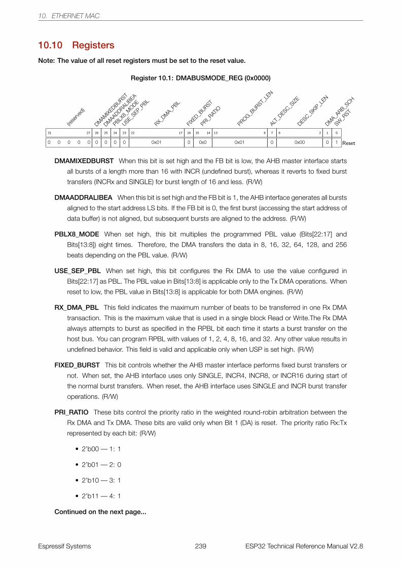
10. ETHERNET MAC
10.10 Registers
Note: The value of all reset registers must be set to the reset value.
Register 10.1: DMABUSMODE_REG (0x0000)
(rese
rved)
0 0 0 0 0
31 27
DMAM
IXEDBURST
0
26
DMAADDRALIB
EA
0
25
PBLX8_
MODE
0
24
USE_SEP_P
BL
0
23
RX_DM
A_PBL
0x01
22 17
FIXED_B
URST
0
16
PRI_RAT
IO
0x0
15 14
PROG_BURST_
LEN
0x01
13 8
ALT_D
ESC_SIZE
0
7
DESC_SKIP
_LEN
0x00
6 2
DMA_A
RB_SCH
0
1
SW_R
ST
1
0
Reset
DMAMIXEDBURST When this bit is set high and the FB bit is low, the AHB master interface starts
all bursts of a length more than 16 with INCR (undefined burst), whereas it reverts to fixed burst
transfers (INCRx and SINGLE) for burst length of 16 and less. (R/W)
DMAADDRALIBEA When this bit is set high and the FB bit is 1, the AHB interface generates all bursts
aligned to the start address LS bits. If the FB bit is 0, the first burst (accessing the start address of
data buffer) is not aligned, but subsequent bursts are aligned to the address. (R/W)
PBLX8_MODE When set high, this bit multiplies the programmed PBL value (Bits[22:17] and
Bits[13:8]) eight times. Therefore, the DMA transfers the data in 8, 16, 32, 64, 128, and 256
beats depending on the PBL value. (R/W)
USE_SEP_PBL When set high, this bit configures the Rx DMA to use the value configured in
Bits[22:17] as PBL. The PBL value in Bits[13:8] is applicable only to the Tx DMA operations. When
reset to low, the PBL value in Bits[13:8] is applicable for both DMA engines. (R/W)
RX_DMA_PBL This field indicates the maximum number of beats to be transferred in one Rx DMA
transaction. This is the maximum value that is used in a single block Read or Write.The Rx DMA
always attempts to burst as specified in the RPBL bit each time it starts a burst transfer on the
host bus. You can program RPBL with values of 1, 2, 4, 8, 16, and 32. Any other value results in
undefined behavior. This field is valid and applicable only when USP is set high. (R/W)
FIXED_BURST This bit controls whether the AHB master interface performs fixed burst transfers or
not. When set, the AHB interface uses only SINGLE, INCR4, INCR8, or INCR16 during start of
the normal burst transfers. When reset, the AHB interface uses SINGLE and INCR burst transfer
operations. (R/W)
PRI_RATIO These bits control the priority ratio in the weighted round-robin arbitration between the
Rx DMA and Tx DMA. These bits are valid only when Bit 1 (DA) is reset. The priority ratio Rx:Tx
represented by each bit: (R/W)
• 2’b00 — 1: 1
• 2’b01 — 2: 0
• 2’b10 — 3: 1
• 2’b11 — 4: 1
Continued on the next page...
Espressif Systems 239 ESP32 Technical Reference Manual V2.8
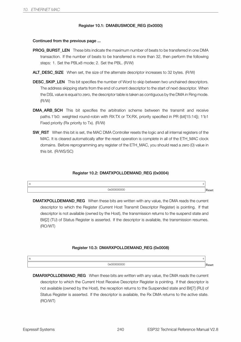
10. ETHERNET MAC
Register 10.1: DMABUSMODE_REG (0x0000)
Continued from the previous page ...
PROG_BURST_LEN These bits indicate the maximum number of beats to be transferred in one DMA
transaction. If the number of beats to be transferred is more than 32, then perform the following
steps: 1. Set the PBLx8 mode; 2. Set the PBL. (R/W)
ALT_DESC_SIZE When set, the size of the alternate descriptor increases to 32 bytes. (R/W)
DESC_SKIP_LEN This bit specifies the number of Word to skip between two unchained descriptors.
The address skipping starts from the end of current descriptor to the start of next descriptor. When
the DSL value is equal to zero, the descriptor table is taken as contiguous by the DMA in Ring mode.
(R/W)
DMA_ARB_SCH This bit specifies the arbitration scheme between the transmit and receive
paths.1’b0: weighted round-robin with RX:TX or TX:RX, priority specified in PR (bit[15:14]); 1’b1
Fixed priority (Rx priority to Tx). (R/W)
SW_RST When this bit is set, the MAC DMA Controller resets the logic and all internal registers of the
MAC. It is cleared automatically after the reset operation is complete in all of the ETH_MAC clock
domains. Before reprogramming any register of the ETH_MAC, you should read a zero (0) value in
this bit. (R/WS/SC)
Register 10.2: DMATXPOLLDEMAND_REG (0x0004)
0x000000000
31 0
Reset
DMATXPOLLDEMAND_REG When these bits are written with any value, the DMA reads the current
descriptor to which the Register (Current Host Transmit Descriptor Register) is pointing. If that
descriptor is not available (owned by the Host), the transmission returns to the suspend state and
Bit[2] (TU) of Status Register is asserted. If the descriptor is available, the transmission resumes.
(RO/WT)
Register 10.3: DMARXPOLLDEMAND_REG (0x0008)
0x000000000
31 0
Reset
DMARXPOLLDEMAND_REG When these bits are written with any value, the DMA reads the current
descriptor to which the Current Host Receive Descriptor Register is pointing. If that descriptor is
not available (owned by the Host), the reception returns to the Suspended state and Bit[7] (RU) of
Status Register is asserted. If the descriptor is available, the Rx DMA returns to the active state.
(RO/WT)
Espressif Systems 240 ESP32 Technical Reference Manual V2.8

10. ETHERNET MAC
Register 10.4: DMARXBASEADDR_REG (0x000C)
0x000000000
31 0
Reset
DMARXBASEADDR_REG This field contains the base address of the first descriptor in the Receive
Descriptor list. The LSB Bits[1:0] are ignored and internally taken as all-zero by the DMA. Therefore,
these LSB bits are read-only. (R/W)
Register 10.5: DMATXBASEADDR_REG (0x0010)
0x000000000
31 0
Reset
DMATXBASEADDR_REG This field contains the base address of the first descriptor in the Transmit
Descriptor list. The LSB Bits[1:0] are ignored and are internally taken as all-zero by the DMA.
Therefore, these LSB bits are read-only. (R/W)
Register 10.6: DMASTATUS_REG (0x0014)
(rese
rved)
0 0
31 30
TS_T
RI_INT
0
29
EMAC_P
MT_
INT
0
28
(rese
rved)
0 0
27 26
ERROR_BITS
0x0
25 23
TRANS_P
ROC_STA
TE
0x0
22 20
RECV_PROC_S
TATE
0x0
19 17
NORM_IN
T_SUM
M
0
16
ABN_INT_
SUMM
0
15
EARLY_R
ECV_INT
0
14
FATA
L_BUS_E
RR_INT
0
13
(rese
rved)
0 0
12 11
EARLY_T
RANS_INT
0
10
RECV_WDT_
TO
0
9
RECV_PROC_S
TOP
0
8
RECV_BUF_
UNAVAIL
0
7
RECV_INT
0
6
TRANS_U
NDFLOW
0
5
RECV_OVFL
OW
0
4
TRANS_J
ABBER_TO
0
3
TRANS_B
UF_UNAV
AIL
0
2
TRANS_P
ROC_STO
P
0
1
TRANS_IN
T
0
0
Reset
TS_TRI_INT This bit indicates an interrupt event in the Timestamp Generator block of the ETH_MAC.
The software must read the corresponding registers in the ETH_MAC to get the exact cause of the
interrupt and clear its source to reset this bit to 1’b0. (RO)
EMAC_PMT_INT This bit indicates an interrupt event in the PMT module of the ETH_MAC. The soft-
ware must read the PMT Control and Status Register in the MAC to get the exact cause of interrupt
and clear its source to reset this bit to 1’b0. (RO)
Continued on the next page...
Espressif Systems 241 ESP32 Technical Reference Manual V2.8
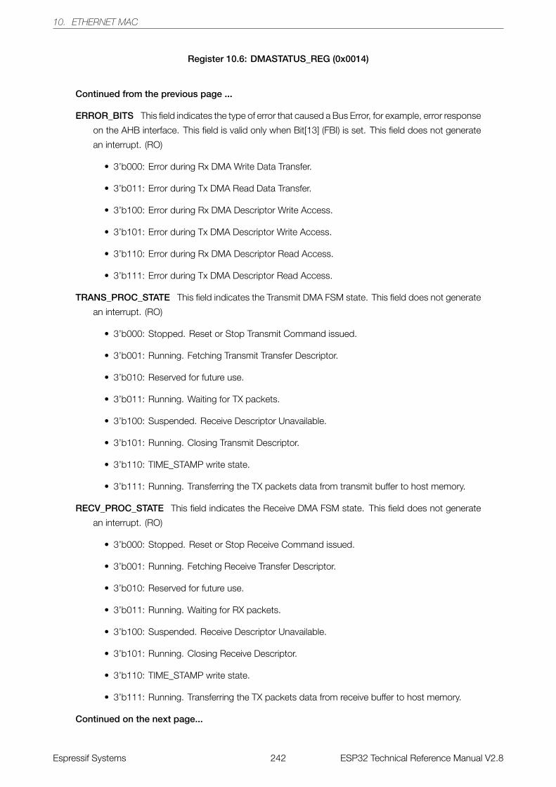
10. ETHERNET MAC
Register 10.6: DMASTATUS_REG (0x0014)
Continued from the previous page ...
ERROR_BITS This field indicates the type of error that caused a Bus Error, for example, error response
on the AHB interface. This field is valid only when Bit[13] (FBI) is set. This field does not generate
an interrupt. (RO)
• 3’b000: Error during Rx DMA Write Data Transfer.
• 3’b011: Error during Tx DMA Read Data Transfer.
• 3’b100: Error during Rx DMA Descriptor Write Access.
• 3’b101: Error during Tx DMA Descriptor Write Access.
• 3’b110: Error during Rx DMA Descriptor Read Access.
• 3’b111: Error during Tx DMA Descriptor Read Access.
TRANS_PROC_STATE This field indicates the Transmit DMA FSM state. This field does not generate
an interrupt. (RO)
• 3’b000: Stopped. Reset or Stop Transmit Command issued.
• 3’b001: Running. Fetching Transmit Transfer Descriptor.
• 3’b010: Reserved for future use.
• 3’b011: Running. Waiting for TX packets.
• 3’b100: Suspended. Receive Descriptor Unavailable.
• 3’b101: Running. Closing Transmit Descriptor.
• 3’b110: TIME_STAMP write state.
• 3’b111: Running. Transferring the TX packets data from transmit buffer to host memory.
RECV_PROC_STATE This field indicates the Receive DMA FSM state. This field does not generate
an interrupt. (RO)
• 3’b000: Stopped. Reset or Stop Receive Command issued.
• 3’b001: Running. Fetching Receive Transfer Descriptor.
• 3’b010: Reserved for future use.
• 3’b011: Running. Waiting for RX packets.
• 3’b100: Suspended. Receive Descriptor Unavailable.
• 3’b101: Running. Closing Receive Descriptor.
• 3’b110: TIME_STAMP write state.
• 3’b111: Running. Transferring the TX packets data from receive buffer to host memory.
Continued on the next page...
Espressif Systems 242 ESP32 Technical Reference Manual V2.8
10. ETHERNET MAC
Register 10.6: DMASTATUS_REG (0x0014)
Continued from the previous page ...
NORM_INT_SUMM Normal Interrupt Summary bit value is the logical OR of the following bits when
the corresponding interrupt bits are enabled in Interrupt Enable Register:(R/SS/WC)
• Bit[0]: Transmit Interrupt.
• Bit[2]: Transmit Buffer Unavailable.
• Bit[6]: Receive Interrupt.
• Bit[14]: Early Receive Interrupt. Only unmasked bits affect the Normal Interrupt Summary bit.
This is a sticky bit and must be cleared (by writing 1 to this bit) each time a corresponding bit,
which causes NIS to be set, is cleared.
ABN_INT_SUMM Abnormal Interrupt Summary bit value is the logical OR of the following when the
corresponding interrupt bits are enabled in Interrupt Enable Register: (R/SS/WC)
• Bit[1]: Transmit Process Stopped.
• Bit[3]: Transmit Jabber Timeout.
• Bit[4]: Receive FIFO Overflow.
• Bit[5]: Transmit Underflow.
• Bit[7]: Receive Buffer Unavailable. Bit[8]: Receive Process Stopped.
• Bit[9]: Receive Watchdog Timeout.
• Bit[10]: Early Transmit Interrupt.
• Bit[13]: Fatal Bus Error. Only unmasked bits affect the Abnormal Interrupt Summary bit. This
is a sticky bit and must be cleared (by writing 1 to this bit) each time a corresponding bit,
which causes AIS to be set, is cleared.
EARLY_RECV_INT This bit indicates that the DMA filled the first data buffer of the packet. This bit is
cleared when the software writes 1 to this bit or when Bit[6] (RI) of this register is set (whichever
occurs earlier). (R/SS/WC)
FATAL_BUS_ERR_INT This bit indicates that a bus error occurred, as described in Bits [25:23]. When
this bit is set, the corresponding DMA engine disables all of its bus accesses. (R/SS/WC)
EARLY_TRANS_INT This bit indicates that the frame to be transmitted is fully transferred to the MTL
Transmit FIFO. (R/SS/WC)
RECV_WDT_TO When set, this bit indicates that the Receive Watchdog Timer expired while receiving
the current frame and the current frame is truncated after the watchdog timeout. (R/SS/WC)
Continued on the next page...
Espressif Systems 243 ESP32 Technical Reference Manual V2.8
10. ETHERNET MAC
Register 10.6: DMASTATUS_REG (0x0014)
Continued from the previous page ...
RECV_PROC_STOP This bit is asserted when the Receive Process enters the Stopped state.
(R/SS/WC)
RECV_BUF_UNAVAIL This bit indicates that the host owns the Next Descriptor in the Receive List and
the DMA cannot acquire it. The Receive Process is suspended. To resume processing Receive
descriptors, the host should change the ownership of the descriptor and issue a Receive Poll
Demand command. If no Receive Poll Demand is issued, the Receive Process resumes when
the next recognized incoming frame is received. This bit is set only when the previous Receive
Descriptor is owned by the DMA. (R/SS/WC)
RECV_INT This bit indicates that the frame reception is complete. When reception is complete, the
Bit[31] of RDES1 (Disable Interrupt on Completion) is reset in the last Descriptor, and the specific
frame status information is updated in the descriptor. The reception remains in the Running state.
(R/SS/WC)
TRANS_UNDFLOW This bit indicates that the Transmit Buffer had an Underflow during frame trans-
mission. Transmission is suspended and an Underflow Error TDES0[1] is set. (R/SS/WC)
RECV_OVFLOW This bit indicates that the Receive Buffer had an Overflow during frame recep-
tion. If the partial frame is transferred to the application, the overflow status is set in RDES0[11].
(R/SS/WC)
TRANS_JABBER_TO This bit indicates that the Transmit Jabber Timer expired, which happens when
the frame size exceeds 2,048 (10,240 bytes when the Jumbo frame is enabled). When the Jabber
Timeout occurs, the transmission process is aborted and placed in the Stopped state. This causes
the Transmit Jabber Timeout TDES0[14] flag to assert. (R/SS/WC)
TRANS_BUF_UNAVAIL This bit indicates that the host owns the Next Descriptor in the Transmit
List and the DMA cannot acquire it. Transmission is suspended. Bits[22:20] explain the Transmit
Process state transitions. To resume processing Transmit descriptors, the host should change
the ownership of the descriptor by setting TDES0[31] and then issue a Transmit Poll Demand
command. (R/SS/WC)
TRANS_PROC_STOP This bit is set when the transmission is stopped. (R/SS/WC)
TRANS_INT This bit indicates that the frame transmission is complete. When transmission is com-
plete, Bit[31] (OWN) of TDES0 is reset, and the specific frame status information is updated in the
descriptor. (R/SS/WC)
Espressif Systems 244 ESP32 Technical Reference Manual V2.8
10. ETHERNET MAC
Register 10.7: DMAIN_EN_REG (0x001C)
(rese
rved)
0 0 0 0 0 0 0 0 0 0 0 0 0 0 0
31 17
DMAIN
_NIS
E
0
16
DMAIN
_AIS
E
0
15
DMAIN
_ERIE
0
14
DMAIN
_FBEE
0
13
(rese
rved)
0 0
12 11
DMAIN
_ETIE
0
10
DMAIN
_RW
TE
0
9
DMAIN
_RSE
0
8
DMAIN
_RBUE
0
7
DMAIN
_RIE
0
6
DMAIN
_UIE
0
5
DMAIN
_OIE
0
4
DMAIN
_TJT
E
0
3
DMAIN
_TBUE
0
2
DMAIN
_TSE
0
1
DMAIN
_TIE
0
0
Reset
DMAIN_NISE When this bit is set, normal interrupt summary is enabled. When this bit is reset, normal
interrupt summary is disabled. This bit enables the following interrupts in Status Register: (R/W)
• Bit[0]: Transmit Interrupt.
• Bit[2]: Transmit Buffer Unavailable.
• Bit[6]: Receive Interrupt.
• Bit[14]: Early Receive Interrupt.
DMAIN_AISE When this bit is set, abnormal interrupt summary is enabled. When this bit is reset,
the abnormal interrupt summary is disabled. This bit enables the following interrupts in Status
Register:(R/W)
• Bit[1]: Transmit Process Stopped.
• Bit[3]: Transmit Jabber Timeout.
• Bit[4]: Receive Overflow.
• Bit[5]: Transmit Underflow.
• Bit[7]: Receive Buffer Unavailable.
• Bit[8]: Receive Process Stopped.
• Bit[9]: Receive Watchdog Timeout.
• Bit[10]: Early Transmit Interrupt.
• Bit[13]: Fatal Bus Error.
DMAIN_ERIE When this bit is set with Normal Interrupt Summary Enable (Bit[16]), the Early Receive
Interrupt is enabled. When this bit is reset, the Early Receive Interrupt is disabled. (R/W)
Continued on the next page...
Espressif Systems 245 ESP32 Technical Reference Manual V2.8
10. ETHERNET MAC
Register 10.7: DMABUSMODE_REG (0x0000)
Continued from the previous page ...
DMAIN_FBEE When this bit is set with Abnormal Interrupt Summary Enable (Bit[15]), the Fatal Bus
Error Interrupt is enabled. When this bit is reset, the Fatal Bus Error Enable Interrupt is disabled.
(R/W)
DMAIN_ETIE When this bit is set with an Abnormal Interrupt Summary Enable (Bit[15]), the Early
Transmit Interrupt is enabled. When this bit is reset, the Early Transmit Interrupt is disabled. (R/W)
DMAIN_RWTE When this bit is set with Abnormal Interrupt Summary Enable (Bit[15]), the Receive
Watchdog Timeout Interrupt is enabled. When this bit is reset, the Receive Watchdog Timeout
Interrupt is disabled. (R/W)
DMAIN_RSE When this bit is set with Abnormal Interrupt Summary Enable (Bit[15]), the Receive
Stopped Interrupt is enabled. When this bit is reset, the Receive Stopped Interrupt is disabled.
(R/W)
DMAIN_RBUE When this bit is set with Abnormal Interrupt Summary Enable (Bit[15]), the Receive
Buffer Unavailable Interrupt is enabled. When this bit is reset, the Receive Buffer Unavailable Inter-
rupt is disabled. (R/W)
DMAIN_RIE When this bit is set with Normal Interrupt Summary Enable (Bit[16]), the Receive Interrupt
is enabled. When this bit is reset, the Receive Interrupt is disabled. (R/W)
DMAIN_UIE When this bit is set with Abnormal Interrupt Summary Enable (Bit[15]), the Transmit Un-
derflow Interrupt is enabled. When this bit is reset, the Underflow Interrupt is disabled. (R/W)
DMAIN_OIE When this bit is set with Abnormal Interrupt Summary Enable (Bit[15]), the Receive Over-
flow Interrupt is enabled. When this bit is reset, the Overflow Interrupt is disabled. (R/W)
DMAIN_TJTE When this bit is set with Abnormal Interrupt Summary Enable (Bit[15]), the Transmit
Jabber Timeout Interrupt is enabled. When this bit is reset, the Transmit Jabber Timeout Interrupt
is disabled. (R/W)
DMAIN_TBUE When this bit is set with Normal Interrupt Summary Enable (Bit 16), the Transmit Buffer
Unavailable Interrupt is enabled. When this bit is reset, the Transmit Buffer Unavailable Interrupt is
disabled. (R/W)
DMAIN_TSE When this bit is set with Abnormal Interrupt Summary Enable (Bit[15]), the Transmission
Stopped Interrupt is enabled. When this bit is reset, the Transmission Stopped Interrupt is disabled.
(R/W)
DMAIN_TIE When this bit is set with Normal Interrupt Summary Enable (Bit[16]), the Transmit Interrupt
is enabled. When this bit is reset, the Transmit Interrupt is disabled. (R/W)
Espressif Systems 246 ESP32 Technical Reference Manual V2.8
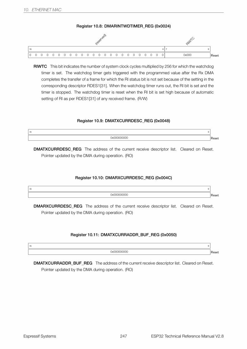
10. ETHERNET MAC
Register 10.8: DMARINTWDTIMER_REG (0x0024)
(rese
rved)
0 0 0 0 0 0 0 0 0 0 0 0 0 0 0 0 0 0 0 0 0 0 0 0
31 8
RIWTC
0x000
7 0
Reset
RIWTC This bit indicates the number of system clock cycles multiplied by 256 for which the watchdog
timer is set. The watchdog timer gets triggered with the programmed value after the Rx DMA
completes the transfer of a frame for which the RI status bit is not set because of the setting in the
corresponding descriptor RDES1[31]. When the watchdog timer runs out, the RI bit is set and the
timer is stopped. The watchdog timer is reset when the RI bit is set high because of automatic
setting of RI as per RDES1[31] of any received frame. (R/W)
Register 10.9: DMATXCURRDESC_REG (0x0048)
0x000000000
31 0
Reset
DMATXCURRDESC_REG The address of the current receive descriptor list. Cleared on Reset.
Pointer updated by the DMA during operation. (RO)
Register 10.10: DMARXCURRDESC_REG (0x004C)
0x000000000
31 0
Reset
DMARXCURRDESC_REG The address of the current receive descriptor list. Cleared on Reset.
Pointer updated by the DMA during operation. (RO)
Register 10.11: DMATXCURRADDR_BUF_REG (0x0050)
0x000000000
31 0
Reset
DMATXCURRADDR_BUF_REG The address of the current receive descriptor list. Cleared on Reset.
Pointer updated by the DMA during operation. (RO)
Espressif Systems 247 ESP32 Technical Reference Manual V2.8
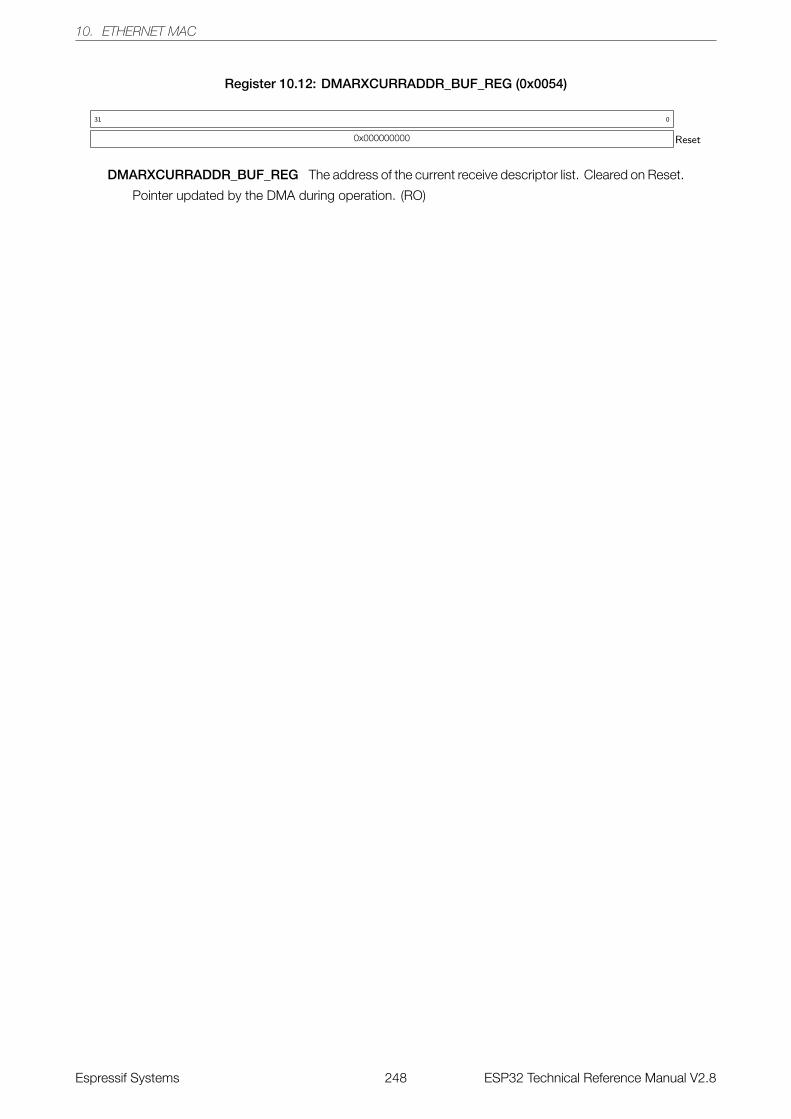
10. ETHERNET MAC
Register 10.12: DMARXCURRADDR_BUF_REG (0x0054)
0x000000000
31 0
Reset
DMARXCURRADDR_BUF_REG The address of the current receive descriptor list. Cleared on Reset.
Pointer updated by the DMA during operation. (RO)
Espressif Systems 248 ESP32 Technical Reference Manual V2.8
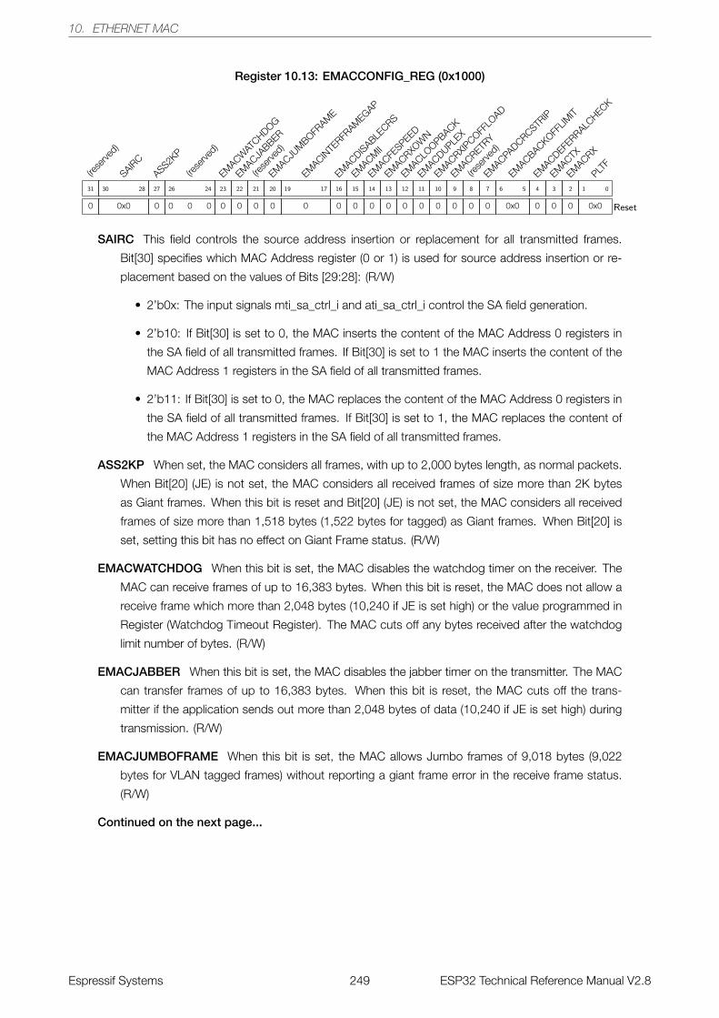
10. ETHERNET MAC
Register 10.13: EMACCONFIG_REG (0x1000)
(rese
rved)
0
31
SAIRC
0x0
30 28
ASS2KP
0
27
(rese
rved)
0 0 0
26 24
EMACW
ATCHDOG
0
23
EMACJA
BBER
0
22
(rese
rved)
0
21
EMACJU
MBOFR
AME
0
20
EMACIN
TERFR
AMEGAP
0
19 17
EMACDIS
ABLECRS
0
16
EMACM
II
0
15
EMACFE
SPEED
0
14
EMACRXO
WN
0
13
EMACLO
OPBACK
0
12
EMACDUPLE
X
0
11
EMACRXIP
COFFLO
AD
0
10
EMACRETR
Y
0
9
(rese
rved)
0
8
EMACPA
DCRCSTRIP
0
7
EMACBACKOFF
LIMIT
0x0
6 5
EMACDEFE
RRALCHECK
0
4
EMACTX
0
3
EMACRX
0
2
PLTF
0x0
1 0
Reset
SAIRC This field controls the source address insertion or replacement for all transmitted frames.
Bit[30] specifies which MAC Address register (0 or 1) is used for source address insertion or re-
placement based on the values of Bits [29:28]: (R/W)
• 2’b0x: The input signals mti_sa_ctrl_i and ati_sa_ctrl_i control the SA field generation.
• 2’b10: If Bit[30] is set to 0, the MAC inserts the content of the MAC Address 0 registers in
the SA field of all transmitted frames. If Bit[30] is set to 1 the MAC inserts the content of the
MAC Address 1 registers in the SA field of all transmitted frames.
• 2’b11: If Bit[30] is set to 0, the MAC replaces the content of the MAC Address 0 registers in
the SA field of all transmitted frames. If Bit[30] is set to 1, the MAC replaces the content of
the MAC Address 1 registers in the SA field of all transmitted frames.
ASS2KP When set, the MAC considers all frames, with up to 2,000 bytes length, as normal packets.
When Bit[20] (JE) is not set, the MAC considers all received frames of size more than 2K bytes
as Giant frames. When this bit is reset and Bit[20] (JE) is not set, the MAC considers all received
frames of size more than 1,518 bytes (1,522 bytes for tagged) as Giant frames. When Bit[20] is
set, setting this bit has no effect on Giant Frame status. (R/W)
EMACWATCHDOG When this bit is set, the MAC disables the watchdog timer on the receiver. The
MAC can receive frames of up to 16,383 bytes. When this bit is reset, the MAC does not allow a
receive frame which more than 2,048 bytes (10,240 if JE is set high) or the value programmed in
Register (Watchdog Timeout Register). The MAC cuts off any bytes received after the watchdog
limit number of bytes. (R/W)
EMACJABBER When this bit is set, the MAC disables the jabber timer on the transmitter. The MAC
can transfer frames of up to 16,383 bytes. When this bit is reset, the MAC cuts off the trans-
mitter if the application sends out more than 2,048 bytes of data (10,240 if JE is set high) during
transmission. (R/W)
EMACJUMBOFRAME When this bit is set, the MAC allows Jumbo frames of 9,018 bytes (9,022
bytes for VLAN tagged frames) without reporting a giant frame error in the receive frame status.
(R/W)
Continued on the next page...
Espressif Systems 249 ESP32 Technical Reference Manual V2.8
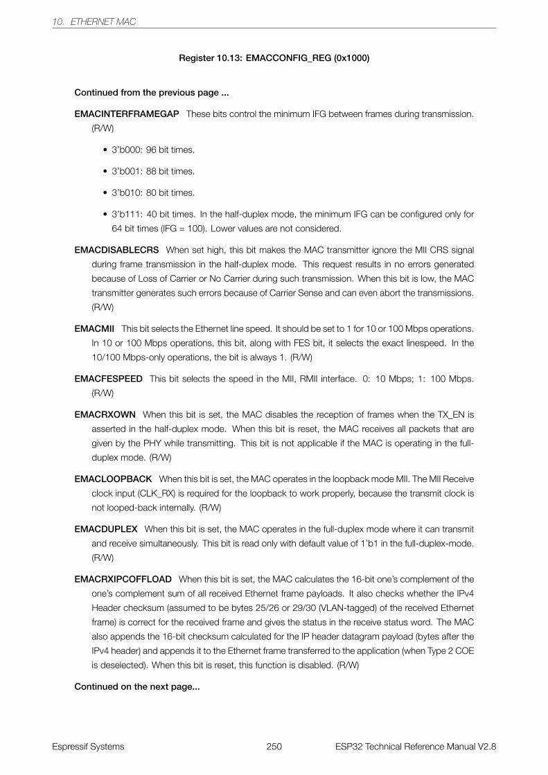
10. ETHERNET MAC
Register 10.13: EMACCONFIG_REG (0x1000)
Continued from the previous page ...
EMACINTERFRAMEGAP These bits control the minimum IFG between frames during transmission.
(R/W)
• 3’b000: 96 bit times.
• 3’b001: 88 bit times.
• 3’b010: 80 bit times.
• 3’b111: 40 bit times. In the half-duplex mode, the minimum IFG can be configured only for
64 bit times (IFG = 100). Lower values are not considered.
EMACDISABLECRS When set high, this bit makes the MAC transmitter ignore the MII CRS signal
during frame transmission in the half-duplex mode. This request results in no errors generated
because of Loss of Carrier or No Carrier during such transmission. When this bit is low, the MAC
transmitter generates such errors because of Carrier Sense and can even abort the transmissions.
(R/W)
EMACMII This bit selects the Ethernet line speed. It should be set to 1 for 10 or 100 Mbps operations.
In 10 or 100 Mbps operations, this bit, along with FES bit, it selects the exact linespeed. In the
10/100 Mbps-only operations, the bit is always 1. (R/W)
EMACFESPEED This bit selects the speed in the MII, RMII interface. 0: 10 Mbps; 1: 100 Mbps.
(R/W)
EMACRXOWN When this bit is set, the MAC disables the reception of frames when the TX_EN is
asserted in the half-duplex mode. When this bit is reset, the MAC receives all packets that are
given by the PHY while transmitting. This bit is not applicable if the MAC is operating in the full-
duplex mode. (R/W)
EMACLOOPBACK When this bit is set, the MAC operates in the loopback mode MII. The MII Receive
clock input (CLK_RX) is required for the loopback to work properly, because the transmit clock is
not looped-back internally. (R/W)
EMACDUPLEX When this bit is set, the MAC operates in the full-duplex mode where it can transmit
and receive simultaneously. This bit is read only with default value of 1’b1 in the full-duplex-mode.
(R/W)
EMACRXIPCOFFLOAD When this bit is set, the MAC calculates the 16-bit one’s complement of the
one’s complement sum of all received Ethernet frame payloads. It also checks whether the IPv4
Header checksum (assumed to be bytes 25/26 or 29/30 (VLAN-tagged) of the received Ethernet
frame) is correct for the received frame and gives the status in the receive status word. The MAC
also appends the 16-bit checksum calculated for the IP header datagram payload (bytes after the
IPv4 header) and appends it to the Ethernet frame transferred to the application (when Type 2 COE
is deselected). When this bit is reset, this function is disabled. (R/W)
Continued on the next page...
Espressif Systems 250 ESP32 Technical Reference Manual V2.8
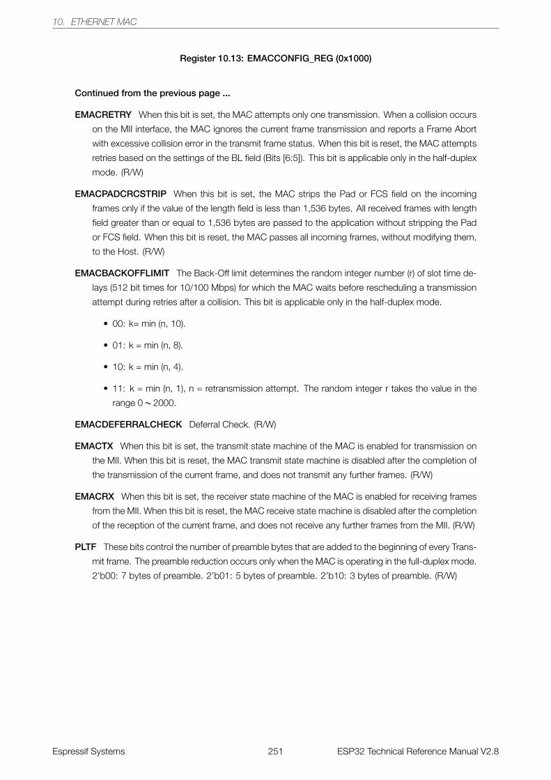
10. ETHERNET MAC
Register 10.13: EMACCONFIG_REG (0x1000)
Continued from the previous page ...
EMACRETRY When this bit is set, the MAC attempts only one transmission. When a collision occurs
on the MII interface, the MAC ignores the current frame transmission and reports a Frame Abort
with excessive collision error in the transmit frame status. When this bit is reset, the MAC attempts
retries based on the settings of the BL field (Bits [6:5]). This bit is applicable only in the half-duplex
mode. (R/W)
EMACPADCRCSTRIP When this bit is set, the MAC strips the Pad or FCS field on the incoming
frames only if the value of the length field is less than 1,536 bytes. All received frames with length
field greater than or equal to 1,536 bytes are passed to the application without stripping the Pad
or FCS field. When this bit is reset, the MAC passes all incoming frames, without modifying them,
to the Host. (R/W)
EMACBACKOFFLIMIT The Back-Off limit determines the random integer number (r) of slot time de-
lays (512 bit times for 10/100 Mbps) for which the MAC waits before rescheduling a transmission
attempt during retries after a collision. This bit is applicable only in the half-duplex mode.
• 00: k= min (n, 10).
• 01: k = min (n, 8).
• 10: k = min (n, 4).
• 11: k = min (n, 1), n = retransmission attempt. The random integer r takes the value in the
range 0 ~ 2000.
EMACDEFERRALCHECK Deferral Check. (R/W)
EMACTX When this bit is set, the transmit state machine of the MAC is enabled for transmission on
the MII. When this bit is reset, the MAC transmit state machine is disabled after the completion of
the transmission of the current frame, and does not transmit any further frames. (R/W)
EMACRX When this bit is set, the receiver state machine of the MAC is enabled for receiving frames
from the MII. When this bit is reset, the MAC receive state machine is disabled after the completion
of the reception of the current frame, and does not receive any further frames from the MII. (R/W)
PLTF These bits control the number of preamble bytes that are added to the beginning of every Trans-
mit frame. The preamble reduction occurs only when the MAC is operating in the full-duplex mode.
2’b00: 7 bytes of preamble. 2’b01: 5 bytes of preamble. 2’b10: 3 bytes of preamble. (R/W)
Espressif Systems 251 ESP32 Technical Reference Manual V2.8
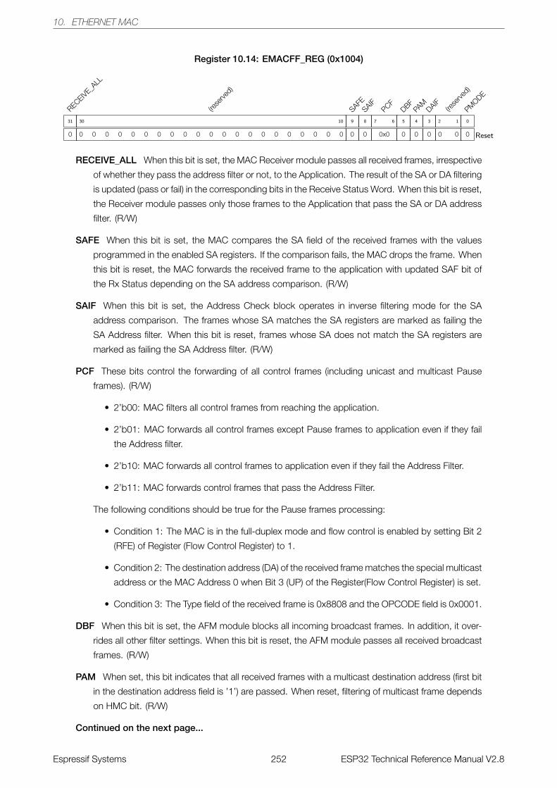
10. ETHERNET MAC
Register 10.14: EMACFF_REG (0x1004)
RECEIVE_ALL
0
31
(rese
rved)
0 0 0 0 0 0 0 0 0 0 0 0 0 0 0 0 0 0 0 0 0
30 10
SAFE
0
9
SAIF
0
8
PCF
0x0
7 6
DBF
0
5
PAM
0
4
DAIF
0
3
(rese
rved)
0 0
2 1
PMODE
0
0
Reset
RECEIVE_ALL When this bit is set, the MAC Receiver module passes all received frames, irrespective
of whether they pass the address filter or not, to the Application. The result of the SA or DA filtering
is updated (pass or fail) in the corresponding bits in the Receive Status Word. When this bit is reset,
the Receiver module passes only those frames to the Application that pass the SA or DA address
filter. (R/W)
SAFE When this bit is set, the MAC compares the SA field of the received frames with the values
programmed in the enabled SA registers. If the comparison fails, the MAC drops the frame. When
this bit is reset, the MAC forwards the received frame to the application with updated SAF bit of
the Rx Status depending on the SA address comparison. (R/W)
SAIF When this bit is set, the Address Check block operates in inverse filtering mode for the SA
address comparison. The frames whose SA matches the SA registers are marked as failing the
SA Address filter. When this bit is reset, frames whose SA does not match the SA registers are
marked as failing the SA Address filter. (R/W)
PCF These bits control the forwarding of all control frames (including unicast and multicast Pause
frames). (R/W)
• 2’b00: MAC filters all control frames from reaching the application.
• 2’b01: MAC forwards all control frames except Pause frames to application even if they fail
the Address filter.
• 2’b10: MAC forwards all control frames to application even if they fail the Address Filter.
• 2’b11: MAC forwards control frames that pass the Address Filter.
The following conditions should be true for the Pause frames processing:
• Condition 1: The MAC is in the full-duplex mode and flow control is enabled by setting Bit 2
(RFE) of Register (Flow Control Register) to 1.
• Condition 2: The destination address (DA) of the received frame matches the special multicast
address or the MAC Address 0 when Bit 3 (UP) of the Register(Flow Control Register) is set.
• Condition 3: The Type field of the received frame is 0x8808 and the OPCODE field is 0x0001.
DBF When this bit is set, the AFM module blocks all incoming broadcast frames. In addition, it over-
rides all other filter settings. When this bit is reset, the AFM module passes all received broadcast
frames. (R/W)
PAM When set, this bit indicates that all received frames with a multicast destination address (first bit
in the destination address field is ’1’) are passed. When reset, filtering of multicast frame depends
on HMC bit. (R/W)
Continued on the next page...
Espressif Systems 252 ESP32 Technical Reference Manual V2.8
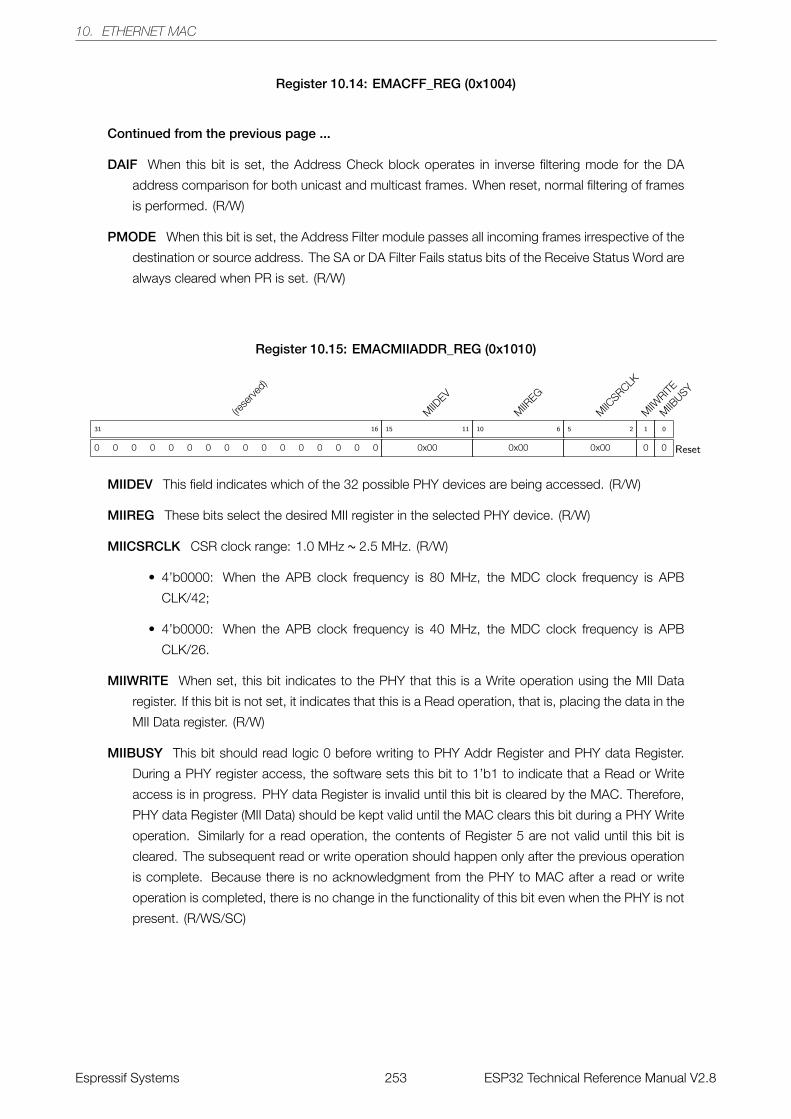
10. ETHERNET MAC
Register 10.14: EMACFF_REG (0x1004)
Continued from the previous page ...
DAIF When this bit is set, the Address Check block operates in inverse filtering mode for the DA
address comparison for both unicast and multicast frames. When reset, normal filtering of frames
is performed. (R/W)
PMODE When this bit is set, the Address Filter module passes all incoming frames irrespective of the
destination or source address. The SA or DA Filter Fails status bits of the Receive Status Word are
always cleared when PR is set. (R/W)
Register 10.15: EMACMIIADDR_REG (0x1010)
(rese
rved)
0 0 0 0 0 0 0 0 0 0 0 0 0 0 0 0
31 16
MIID
EV
0x00
15 11
MIIR
EG
0x00
10 6
MIIC
SRCLK
0x00
5 2
MIIW
RITE
0
1
MIIB
USY
0
0
Reset
MIIDEV This field indicates which of the 32 possible PHY devices are being accessed. (R/W)
MIIREG These bits select the desired MII register in the selected PHY device. (R/W)
MIICSRCLK CSR clock range: 1.0 MHz ~ 2.5 MHz. (R/W)
• 4’b0000: When the APB clock frequency is 80 MHz, the MDC clock frequency is APB
CLK/42;
• 4’b0000: When the APB clock frequency is 40 MHz, the MDC clock frequency is APB
CLK/26.
MIIWRITE When set, this bit indicates to the PHY that this is a Write operation using the MII Data
register. If this bit is not set, it indicates that this is a Read operation, that is, placing the data in the
MII Data register. (R/W)
MIIBUSY This bit should read logic 0 before writing to PHY Addr Register and PHY data Register.
During a PHY register access, the software sets this bit to 1’b1 to indicate that a Read or Write
access is in progress. PHY data Register is invalid until this bit is cleared by the MAC. Therefore,
PHY data Register (MII Data) should be kept valid until the MAC clears this bit during a PHY Write
operation. Similarly for a read operation, the contents of Register 5 are not valid until this bit is
cleared. The subsequent read or write operation should happen only after the previous operation
is complete. Because there is no acknowledgment from the PHY to MAC after a read or write
operation is completed, there is no change in the functionality of this bit even when the PHY is not
present. (R/WS/SC)
Espressif Systems 253 ESP32 Technical Reference Manual V2.8
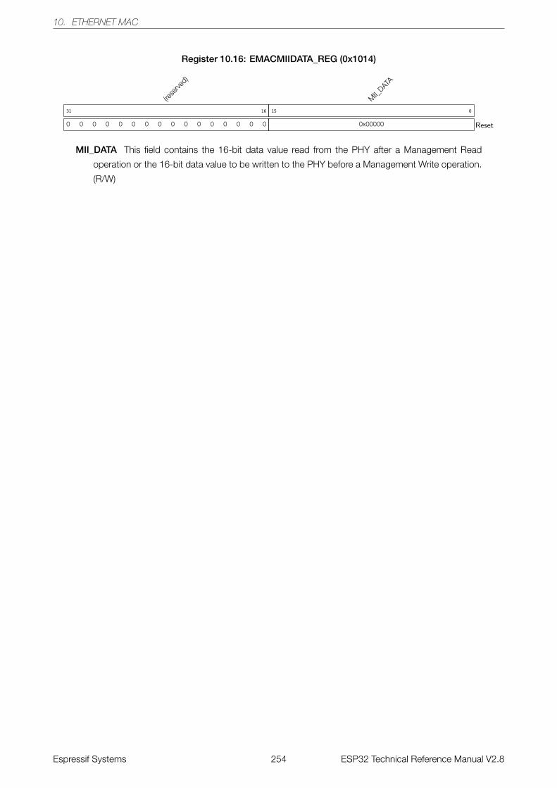
10. ETHERNET MAC
Register 10.16: EMACMIIDATA_REG (0x1014)
(rese
rved)
0 0 0 0 0 0 0 0 0 0 0 0 0 0 0 0
31 16
MII_
DATA
0x00000
15 0
Reset
MII_DATA This field contains the 16-bit data value read from the PHY after a Management Read
operation or the 16-bit data value to be written to the PHY before a Management Write operation.
(R/W)
Espressif Systems 254 ESP32 Technical Reference Manual V2.8

10. ETHERNET MAC
Register 10.17: EMACFC_REG (0x1018)
PAUSE_T
IME
0x00000
31 16
(rese
rved)
0 0 0 0 0 0 0 0 0 0
15 6
PLT
0x0
5 4
UPFD
0
3
RFCE
0
2
TFCE
0
1
FCBBA
0
0
Reset
PAUSE_TIME This field holds the value to be used in the Pause Time field in the transmit control
frame. If the Pause Time bits is configured to be double-synchronized to the MII clock domain,
then consecutive writes to this register should be performed only after at least four clock cycles in
the destination clock domain. (R/W)
PLT This field configures the threshold of the Pause timer automatic retransmission of the Pause frame.
The threshold values should be always less than the Pause Time configured in Bits[31:16]. For
example, if PT = 100H (256 slot-times), and PLT = 01, then a second Pause frame is automatically
transmitted at 228 (256-28) slot times after the first Pause frame is transmitted. The following list
provides the threshold values for different values: (R/W)
• 2’b00: The threshold is Pause time minus 4 slot times (PT-4 slot times).
• 2’b01: The threshold is Pause time minus 28 slot times (PT-28 slot times).
• 2’b10: The threshold is Pause time minus 144 slot times (PT-144 slot times).
• 2’b11: The threshold is Pause time minus 256 slot times (PT-256 slot times). The slot time is
defined as the time taken to transmit 512 bits (64 bytes) on the MII interface.
UPFD A pause frame is processed when it has the unique multicast address specified in the IEEE
Std 802.3. When this bit is set, the MAC can also detect Pause frames with unicast address of
the station. This unicast address should be as specified in the EMACADDR0 High Register and
EMACADDR0 Low Register. When this bit is reset, the MAC only detects Pause frames with unique
multicast address. (R/W)
RFCE When this bit is set, the MAC decodes the received Pause frame and disables its transmitter for
a specified (Pause) time. When this bit is reset, the decode function of the Pause frame is disabled.
(R/W)
TFCE In the full-duplex mode, when this bit is set, the MAC enables the flow control operation to
transmit Pause frames. When this bit is reset, the flow control operation in the MAC is disabled,
and the MAC does not transmit any Pause frames. In the half-duplex mode, when this bit is set,
the MAC enables the backpressure operation. When this bit is reset, the backpressure feature is
disabled. (R/W)
FCBBA This bit initiates a Pause frame in the full-duplex mode and activates the backpressure function
in the half-duplex mode if the TFE bit is set. In the full-duplex mode, this bit should be read as 1’b0
before writing to the Flow Control register. To initiate a Pause frame, the Application must set this
bit to 1’b1. During a transfer of the Control Frame, this bit continues to be set to signify that a
frame transmission is in progress. After the completion of Pause frame transmission, the MAC
resets this bit to 1’b0. The Flow Control register should not be written to until this bit is cleared. In
the half-duplex mode, when this bit is set (and TFE is set), then backpressure is asserted by the
MAC. During backpressure, when the MAC receives a new frame, the transmitter starts sending
a JAM pattern resulting in a collision. When the MAC is configured for the full-duplex mode, the
BPA is automatically disabled. (R/WS/SC)(FCB)/(R/W)(BPA)Espressif Systems 255 ESP32 Technical Reference Manual V2.8
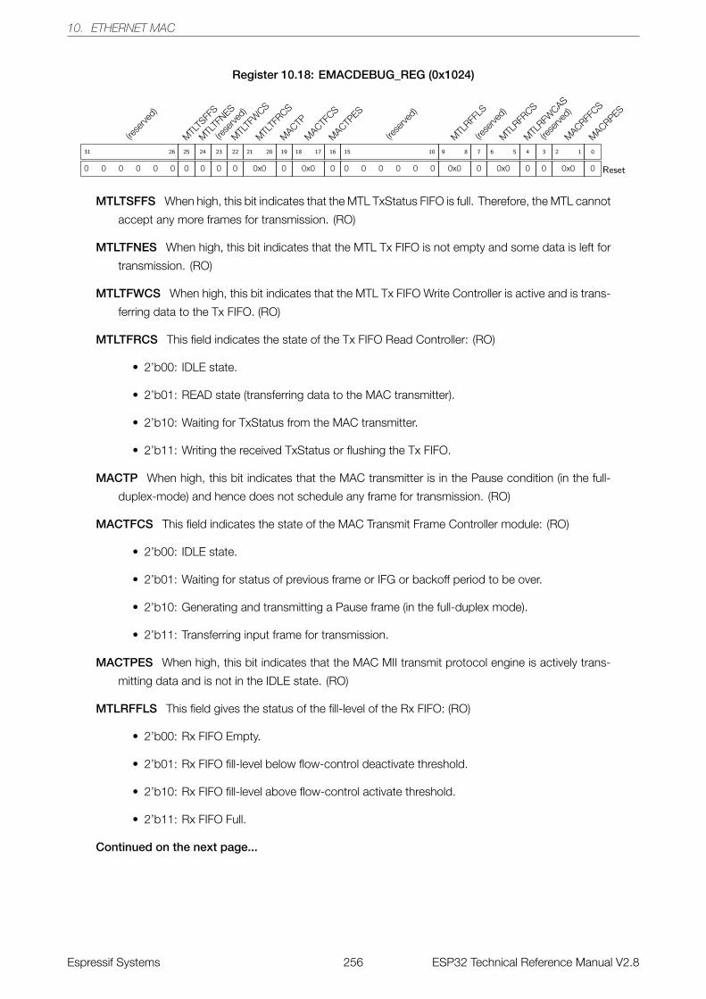
10. ETHERNET MAC
Register 10.18: EMACDEBUG_REG (0x1024)
(rese
rved)
0 0 0 0 0 0
31 26
MTL
TSFF
S
0
25
MTL
TFNES
0
24
(rese
rved)
0
23
MTL
TFW
CS
0
22
MTL
TFRCS
0x0
21 20
MACTP
0
19
MACTF
CS
0x0
18 17
MACTP
ES
0
16
(rese
rved)
0 0 0 0 0 0
15 10
MTL
RFFLS
0x0
9 8
(rese
rved)
0
7
MTL
RFRCS
0x0
6 5
MTL
RFWCAS
0
4
(rese
rved)
0
3
MACRFF
CS
0x0
2 1
MACRPES
0
0
Reset
MTLTSFFS When high, this bit indicates that the MTL TxStatus FIFO is full. Therefore, the MTL cannot
accept any more frames for transmission. (RO)
MTLTFNES When high, this bit indicates that the MTL Tx FIFO is not empty and some data is left for
transmission. (RO)
MTLTFWCS When high, this bit indicates that the MTL Tx FIFO Write Controller is active and is trans-
ferring data to the Tx FIFO. (RO)
MTLTFRCS This field indicates the state of the Tx FIFO Read Controller: (RO)
• 2’b00: IDLE state.
• 2’b01: READ state (transferring data to the MAC transmitter).
• 2’b10: Waiting for TxStatus from the MAC transmitter.
• 2’b11: Writing the received TxStatus or flushing the Tx FIFO.
MACTP When high, this bit indicates that the MAC transmitter is in the Pause condition (in the full-
duplex-mode) and hence does not schedule any frame for transmission. (RO)
MACTFCS This field indicates the state of the MAC Transmit Frame Controller module: (RO)
• 2’b00: IDLE state.
• 2’b01: Waiting for status of previous frame or IFG or backoff period to be over.
• 2’b10: Generating and transmitting a Pause frame (in the full-duplex mode).
• 2’b11: Transferring input frame for transmission.
MACTPES When high, this bit indicates that the MAC MII transmit protocol engine is actively trans-
mitting data and is not in the IDLE state. (RO)
MTLRFFLS This field gives the status of the fill-level of the Rx FIFO: (RO)
• 2’b00: Rx FIFO Empty.
• 2’b01: Rx FIFO fill-level below flow-control deactivate threshold.
• 2’b10: Rx FIFO fill-level above flow-control activate threshold.
• 2’b11: Rx FIFO Full.
Continued on the next page...
Espressif Systems 256 ESP32 Technical Reference Manual V2.8
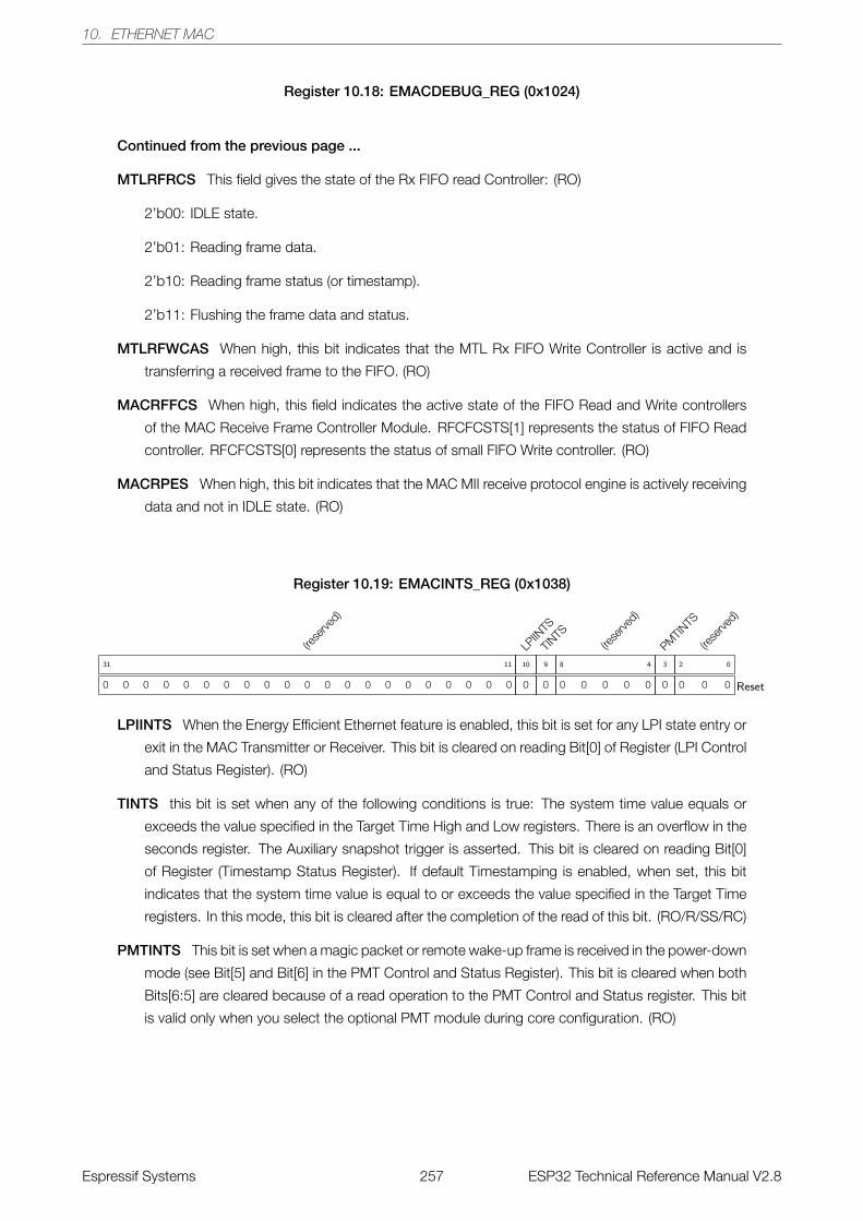
10. ETHERNET MAC
Register 10.18: EMACDEBUG_REG (0x1024)
Continued from the previous page ...
MTLRFRCS This field gives the state of the Rx FIFO read Controller: (RO)
2’b00: IDLE state.
2’b01: Reading frame data.
2’b10: Reading frame status (or timestamp).
2’b11: Flushing the frame data and status.
MTLRFWCAS When high, this bit indicates that the MTL Rx FIFO Write Controller is active and is
transferring a received frame to the FIFO. (RO)
MACRFFCS When high, this field indicates the active state of the FIFO Read and Write controllers
of the MAC Receive Frame Controller Module. RFCFCSTS[1] represents the status of FIFO Read
controller. RFCFCSTS[0] represents the status of small FIFO Write controller. (RO)
MACRPES When high, this bit indicates that the MAC MII receive protocol engine is actively receiving
data and not in IDLE state. (RO)
Register 10.19: EMACINTS_REG (0x1038)
(rese
rved)
0 0 0 0 0 0 0 0 0 0 0 0 0 0 0 0 0 0 0 0 0
31 11
LPIIN
TS
0
10
TINTS
0
9
(rese
rved)
0 0 0 0 0
8 4
PMTIN
TS
0
3
(rese
rved)
0 0 0
2 0
Reset
LPIINTS When the Energy Efficient Ethernet feature is enabled, this bit is set for any LPI state entry or
exit in the MAC Transmitter or Receiver. This bit is cleared on reading Bit[0] of Register (LPI Control
and Status Register). (RO)
TINTS this bit is set when any of the following conditions is true: The system time value equals or
exceeds the value specified in the Target Time High and Low registers. There is an overflow in the
seconds register. The Auxiliary snapshot trigger is asserted. This bit is cleared on reading Bit[0]
of Register (Timestamp Status Register). If default Timestamping is enabled, when set, this bit
indicates that the system time value is equal to or exceeds the value specified in the Target Time
registers. In this mode, this bit is cleared after the completion of the read of this bit. (RO/R/SS/RC)
PMTINTS This bit is set when a magic packet or remote wake-up frame is received in the power-down
mode (see Bit[5] and Bit[6] in the PMT Control and Status Register). This bit is cleared when both
Bits[6:5] are cleared because of a read operation to the PMT Control and Status register. This bit
is valid only when you select the optional PMT module during core configuration. (RO)
Espressif Systems 257 ESP32 Technical Reference Manual V2.8
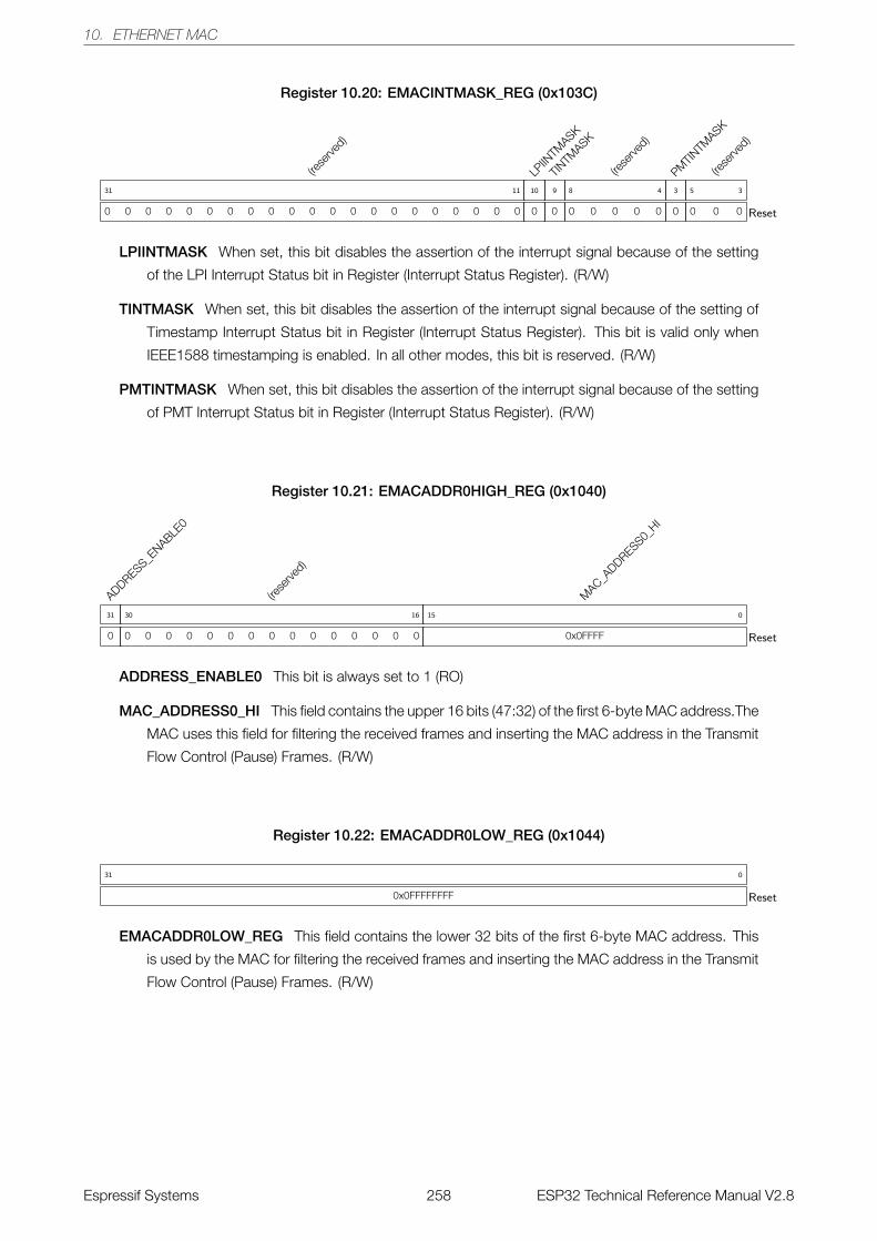
10. ETHERNET MAC
Register 10.20: EMACINTMASK_REG (0x103C)
(rese
rved)
0 0 0 0 0 0 0 0 0 0 0 0 0 0 0 0 0 0 0 0 0
31 11
LPIIN
TMASK
0
10
TINTM
ASK
0
9
(rese
rved)
0 0 0 0 0
8 4
PMTIN
TMASK
0
3
(rese
rved)
0 0 0
5 3
Reset
LPIINTMASK When set, this bit disables the assertion of the interrupt signal because of the setting
of the LPI Interrupt Status bit in Register (Interrupt Status Register). (R/W)
TINTMASK When set, this bit disables the assertion of the interrupt signal because of the setting of
Timestamp Interrupt Status bit in Register (Interrupt Status Register). This bit is valid only when
IEEE1588 timestamping is enabled. In all other modes, this bit is reserved. (R/W)
PMTINTMASK When set, this bit disables the assertion of the interrupt signal because of the setting
of PMT Interrupt Status bit in Register (Interrupt Status Register). (R/W)
Register 10.21: EMACADDR0HIGH_REG (0x1040)
ADDRESS_ENABLE
0
0
31
(rese
rved)
0 0 0 0 0 0 0 0 0 0 0 0 0 0 0
30 16
MAC_A
DDRESS0_HI
0x0FFFF
15 0
Reset
ADDRESS_ENABLE0 This bit is always set to 1 (RO)
MAC_ADDRESS0_HI This field contains the upper 16 bits (47:32) of the first 6-byte MAC address.The
MAC uses this field for filtering the received frames and inserting the MAC address in the Transmit
Flow Control (Pause) Frames. (R/W)
Register 10.22: EMACADDR0LOW_REG (0x1044)
0x0FFFFFFFF
31 0
Reset
EMACADDR0LOW_REG This field contains the lower 32 bits of the first 6-byte MAC address. This
is used by the MAC for filtering the received frames and inserting the MAC address in the Transmit
Flow Control (Pause) Frames. (R/W)
Espressif Systems 258 ESP32 Technical Reference Manual V2.8
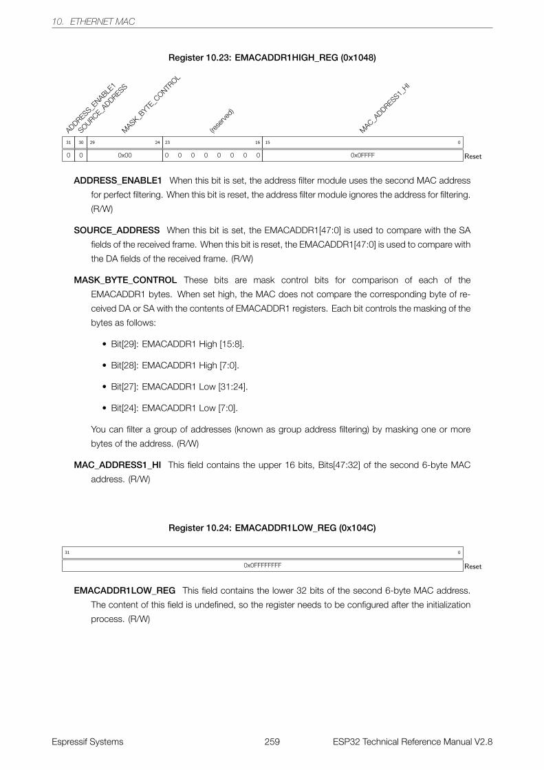
10. ETHERNET MAC
Register 10.23: EMACADDR1HIGH_REG (0x1048)
ADDRESS_ENABLE
1
0
31
SOURCE_ADDRESS
0
30
MASK_B
YTE_C
ONTROL
0x00
29 24
(rese
rved)
0 0 0 0 0 0 0 0
23 16
MAC_A
DDRESS1_HI
0x0FFFF
15 0
Reset
ADDRESS_ENABLE1 When this bit is set, the address filter module uses the second MAC address
for perfect filtering. When this bit is reset, the address filter module ignores the address for filtering.
(R/W)
SOURCE_ADDRESS When this bit is set, the EMACADDR1[47:0] is used to compare with the SA
fields of the received frame. When this bit is reset, the EMACADDR1[47:0] is used to compare with
the DA fields of the received frame. (R/W)
MASK_BYTE_CONTROL These bits are mask control bits for comparison of each of the
EMACADDR1 bytes. When set high, the MAC does not compare the corresponding byte of re-
ceived DA or SA with the contents of EMACADDR1 registers. Each bit controls the masking of the
bytes as follows:
• Bit[29]: EMACADDR1 High [15:8].
• Bit[28]: EMACADDR1 High [7:0].
• Bit[27]: EMACADDR1 Low [31:24].
• Bit[24]: EMACADDR1 Low [7:0].
You can filter a group of addresses (known as group address filtering) by masking one or more
bytes of the address. (R/W)
MAC_ADDRESS1_HI This field contains the upper 16 bits, Bits[47:32] of the second 6-byte MAC
address. (R/W)
Register 10.24: EMACADDR1LOW_REG (0x104C)
0x0FFFFFFFF
31 0
Reset
EMACADDR1LOW_REG This field contains the lower 32 bits of the second 6-byte MAC address.
The content of this field is undefined, so the register needs to be configured after the initialization
process. (R/W)
Espressif Systems 259 ESP32 Technical Reference Manual V2.8
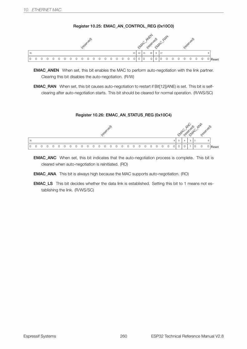
10. ETHERNET MAC
Register 10.25: EMAC_AN_CONTROL_REG (0x10C0)
(rese
rved)
0 0 0 0 0 0 0 0 0 0 0 0 0 0 0 0 0 0 0
31 13
EMAC_A
NEN
0
12
(rese
rved)
0 0
11 10
EMAC_R
AN
0
9
(rese
rved)
0 0 0 0 0 0 0 0 0
17 9
Reset
EMAC_ANEN When set, this bit enables the MAC to perform auto-negotiation with the link partner.
Clearing this bit disables the auto-negotiation. (R/W)
EMAC_RAN When set, this bit causes auto-negotiation to restart if Bit[12](ANE) is set. This bit is self-
clearing after auto-negotiation starts. This bit should be cleared for normal operation. (R/WS/SC)
Register 10.26: EMAC_AN_STATUS_REG (0x10C4)
(rese
rved)
0 0 0 0 0 0 0 0 0 0 0 0 0 0 0 0 0 0 0 0 0 0 0 0 0 0
31 6
EMAC_A
NC
0
5
(rese
rved)
0
4
EMAC_A
NA
1
3
(rese
rved)
0 0 0
2 0
Reset
EMAC_ANC When set, this bit indicates that the auto-negotiation process is complete. This bit is
cleared when auto-negotiation is reinitiated. (RO)
EMAC_ANA This bit is always high because the MAC supports auto-negotiation. (RO)
EMAC_LS This bit decides whether the data link is established. Setting this bit to 1 means not es-
tablishing the link. (R/WS/SC)
Espressif Systems 260 ESP32 Technical Reference Manual V2.8

10. ETHERNET MAC
Register 10.27: EMACCSTATUS_REG (0x10D8)
(rese
rved)
0 0 0 0 0 0 0 0 0 0 0 0 0 0 0
31 17
SMID
RXS
0
16
(rese
rved)
0 0 0 0 0 0 0 0 0 0 0
15 5
(JABBER_T
IMEOUT)
0
4
(rese
rved)
0
3
LINK_S
PEED
0
2 1
LINK_M
ODE
0
0
Reset
JABBER_TIMEOUT This bit indicates whether there is jabber timeout error (1’b1) in the received
frame. (RO)
LINK_SPEED This bit indicates the current speed of the link: (RO)
• 2’b00: 2.5 MHz.
• 2’b01: 25 MHz.
• 2’b10: 125 MHz.
LINK_MODE This bit indicates the current mode of operation of the link: (RO)
• 1’b0: Half-duplex mode.
• 1’b1: Full-duplex mode.
Register 10.28: EMACWDOGTO_REG (0x10DC)
(rese
rved)
0 0 0 0 0 0 0 0 0 0 0 0 0 0 0
31 17
PWDOGEN
0
16
(rese
rved)
0 0
15 14
WDOGTO
0x0000
13 0
Reset
PWDOGEN When this bit is set and Bit[23] (WD) of EMACCONFIG_REG is reset, the WTO field
(Bits[13:0]) is used as watchdog timeout for a received frame. When this bit is cleared, the watch-
dog timeout for a received frame is controlled by the setting of Bit[23] (WD) and Bit[20] (JE) in
EMACCONFIG_REG. (R/W)
WDOGTO When Bit[16] (PWE) is set and Bit[23] (WD) of EMACCONFIG_REG is reset, this field is used
as watchdog timeout for a received frame. If the length of a received frame exceeds the value of
this field, such frame is terminated and declared as an error frame. (R/W)
Espressif Systems 261 ESP32 Technical Reference Manual V2.8
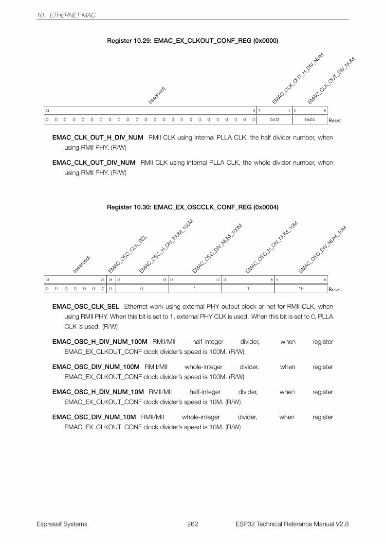
10. ETHERNET MAC
Register 10.29: EMAC_EX_CLKOUT_CONF_REG (0x0000)
(rese
rved)
0 0 0 0 0 0 0 0 0 0 0 0 0 0 0 0 0 0 0 0 0 0 0 0
31 8
EMAC_C
LK_O
UT_H_D
IV_NUM
0x02
7 4
EMAC_C
LK_O
UT_DIV_N
UM
0x04
3 0
Reset
EMAC_CLK_OUT_H_DIV_NUM RMII CLK using internal PLLA CLK, the half divider number, when
using RMII PHY. (R/W)
EMAC_CLK_OUT_DIV_NUM RMII CLK using internal PLLA CLK, the whole divider number, when
using RMII PHY. (R/W)
Register 10.30: EMAC_EX_OSCCLK_CONF_REG (0x0004)
(rese
rved)
0 0 0 0 0 0 0
31 25
EMAC_O
SC_CLK
_SEL
0
24
EMAC_O
SC_H_D
IV_NUM
_100
M
0
23 18
EMAC_O
SC_DIV_N
UM_1
00M
1
17 12
EMAC_O
SC_H_D
IV_NUM
_10M
9
11 6
EMAC_O
SC_DIV_N
UM_1
0M
19
5 0
Reset
EMAC_OSC_CLK_SEL Ethernet work using external PHY output clock or not for RMII CLK, when
using RMII PHY. When this bit is set to 1, external PHY CLK is used. When this bit is set to 0, PLLA
CLK is used. (R/W)
EMAC_OSC_H_DIV_NUM_100M RMII/MII half-integer divider, when register
EMAC_EX_CLKOUT_CONF clock divider’s speed is 100M. (R/W)
EMAC_OSC_DIV_NUM_100M RMII/MII whole-integer divider, when register
EMAC_EX_CLKOUT_CONF clock divider’s speed is 100M. (R/W)
EMAC_OSC_H_DIV_NUM_10M RMII/MII half-integer divider, when register
EMAC_EX_CLKOUT_CONF clock divider’s speed is 10M. (R/W)
EMAC_OSC_DIV_NUM_10M RMII/MII whole-integer divider, when register
EMAC_EX_CLKOUT_CONF clock divider’s speed is 10M. (R/W)
Espressif Systems 262 ESP32 Technical Reference Manual V2.8
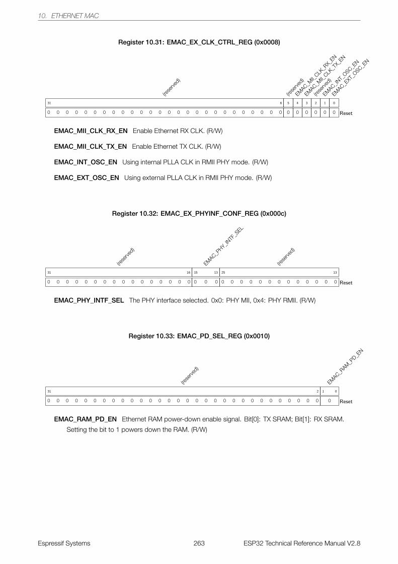
10. ETHERNET MAC
Register 10.31: EMAC_EX_CLK_CTRL_REG (0x0008)
(rese
rved)
0 0 0 0 0 0 0 0 0 0 0 0 0 0 0 0 0 0 0 0 0 0 0 0 0 0
31 6
(rese
rved)
0
5
EMAC_M
II_CLK
_RX_
EN
0
4
EMAC_M
II_CLK
_TX_
EN
0
3
(rese
rved)
0
2
EMAC_IN
T_OSC_E
N
0
1
EMAC_E
XT_O
SC_EN
0
0
Reset
EMAC_MII_CLK_RX_EN Enable Ethernet RX CLK. (R/W)
EMAC_MII_CLK_TX_EN Enable Ethernet TX CLK. (R/W)
EMAC_INT_OSC_EN Using internal PLLA CLK in RMII PHY mode. (R/W)
EMAC_EXT_OSC_EN Using external PLLA CLK in RMII PHY mode. (R/W)
Register 10.32: EMAC_EX_PHYINF_CONF_REG (0x000c)
(rese
rved)
0 0 0 0 0 0 0 0 0 0 0 0 0 0 0 0
31 16
EMAC_P
HY_INTF
_SEL
0 0 0
15 13
(rese
rved)
0 0 0 0 0 0 0 0 0 0 0 0 0
25 13
Reset
EMAC_PHY_INTF_SEL The PHY interface selected. 0x0: PHY MII, 0x4: PHY RMII. (R/W)
Register 10.33: EMAC_PD_SEL_REG (0x0010)
(rese
rved)
0 0 0 0 0 0 0 0 0 0 0 0 0 0 0 0 0 0 0 0 0 0 0 0 0 0 0 0 0 0
31 2
EMAC_R
AM_P
D_EN
0
1 0
Reset
EMAC_RAM_PD_EN Ethernet RAM power-down enable signal. Bit[0]: TX SRAM; Bit[1]: RX SRAM.
Setting the bit to 1 powers down the RAM. (R/W)
Espressif Systems 263 ESP32 Technical Reference Manual V2.8
11. I2C CONTROLLER
11. I2C Controller
11.1 Overview
An I2C (Inter-Integrated Circuit) bus can be used for communication with several external devices connected to
the same bus as ESP32. The ESP32 has dedicated hardware to communicate with peripherals on the I2C
bus.
11.2 Features
The I2C controller has the following features:
• Supports both master mode and slave mode
• Supports multi-master and multi-slave communication
• Supports standard mode (100 kbit/s)
• Supports fast mode (400 kbit/s)
• Supports 7-bit addressing and 10-bit addressing
• Supports continuous data transmission with disabled Serial Clock Line (SCL)
• Supports programmable digital noise filter
11.3 Functional Description
11.3.1 Introduction
I2C is a two-wire bus, consisting of an SDA and an SCL line. These lines are configured to open the drain output.
The lines are shared by two or more devices: usually one or more masters and one or more slaves.
Communication starts when a master sends out a start condition: it will pull the SDA line low, and will then pull
the SCL line high. It will send out nine clock pulses over the SCL line. The first eight pulses are used to shift out a
byte consisting of a 7-bit address and a read/write bit. If a slave with this address is active on the bus, the slave
can answer by pulling the SDA low on the ninth clock pulse. The master can then send out more 9-bit clock
pulse clusters and, depending on the read/write bit sent, the device or the master will shift out data on the SDA
line, with the other side acknowledging the transfer by pulling the SDA low on the ninth clock pulse. During data
transfer, the SDA line changes only when the SCL line is low. When the master has finished the communication, it
will send a stop condition on the bus by raising SDA, while SCL will already be high.
The ESP32 I2C peripheral can handle the I2C protocol, freeing up the processor cores for other tasks.
Espressif Systems 264 ESP32 Technical Reference Manual V2.8
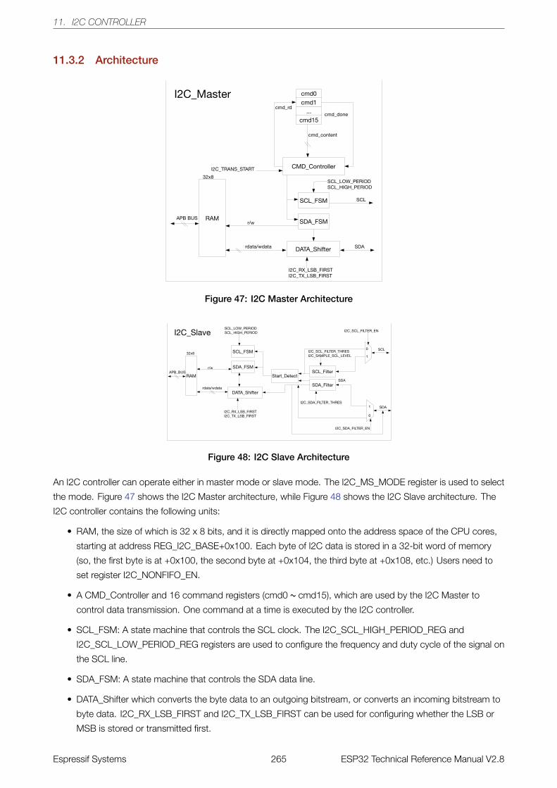
11. I2C CONTROLLER
11.3.2 Architecture
Figure 47: I2C Master Architecture
Figure 48: I2C Slave Architecture
An I2C controller can operate either in master mode or slave mode. The I2C_MS_MODE register is used to select
the mode. Figure 47 shows the I2C Master architecture, while Figure 48 shows the I2C Slave architecture. The
I2C controller contains the following units:
• RAM, the size of which is 32 x 8 bits, and it is directly mapped onto the address space of the CPU cores,
starting at address REG_I2C_BASE+0x100. Each byte of I2C data is stored in a 32-bit word of memory
(so, the first byte is at +0x100, the second byte at +0x104, the third byte at +0x108, etc.) Users need to
set register I2C_NONFIFO_EN.
• A CMD_Controller and 16 command registers (cmd0 ~ cmd15), which are used by the I2C Master to
control data transmission. One command at a time is executed by the I2C controller.
• SCL_FSM: A state machine that controls the SCL clock. The I2C_SCL_HIGH_PERIOD_REG and
I2C_SCL_LOW_PERIOD_REG registers are used to configure the frequency and duty cycle of the signal on
the SCL line.
• SDA_FSM: A state machine that controls the SDA data line.
• DATA_Shifter which converts the byte data to an outgoing bitstream, or converts an incoming bitstream to
byte data. I2C_RX_LSB_FIRST and I2C_TX_LSB_FIRST can be used for configuring whether the LSB or
MSB is stored or transmitted first.
Espressif Systems 265 ESP32 Technical Reference Manual V2.8
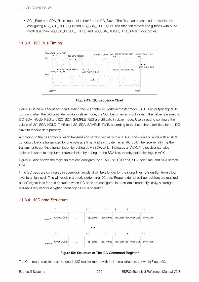
11. I2C CONTROLLER
• SCL_Filter and SDA_Filter: Input noise filter for the I2C_Slave. The filter can be enabled or disabled by
configuring I2C_SCL_FILTER_EN and I2C_SDA_FILTER_EN. The filter can remove line glitches with pulse
width less than I2C_SCL_FILTER_THRES and I2C_SDA_FILTER_THRES ABP clock cycles.
11.3.3 I2C Bus Timing
Figure 49: I2C Sequence Chart
Figure 49 is an I2C sequence chart. When the I2C controller works in master mode, SCL is an output signal. In
contrast, when the I2C controller works in slave mode, the SCL becomes an input signal. The values assigned to
I2C_SDA_HOLD_REG and I2C_SDA_SAMPLE_REG are still valid in slave mode. Users need to configure the
values of I2C_SDA_HOLD_TIME and I2C_SDA_SAMPLE_TIME, according to the host characteristics, for the I2C
slave to receive data properly.
According to the I2C protocol, each transmission of data begins with a START condition and ends with a STOP
condition. Data is transmitted by one byte at a time, and each byte has an ACK bit. The receiver informs the
transmitter to continue transmission by pulling down SDA, which indicates an ACK. The receiver can also
indicate it wants to stop further transmission by pulling up the SDA line, thereby not indicating an ACK.
Figure 49 also shows the registers that can configure the START bit, STOP bit, SDA hold time, and SDA sample
time.
If the I2C pads are configured in open-drain mode, it will take longer for the signal lines to transition from a low
level to a high level. This will result in a poorly performing I2C bus. Proper external pull-up resistors are required
on I2C signal lines for bus operation when I2C pads are configured in open-drain mode. Typically, a stronger
pull-up is required for a higher frequency I2C bus operation.
11.3.4 I2C cmd Structure
Figure 50: Structure of The I2C Command Register
The Command register is active only in I2C master mode, with its internal structure shown in Figure 50.
Espressif Systems 266 ESP32 Technical Reference Manual V2.8
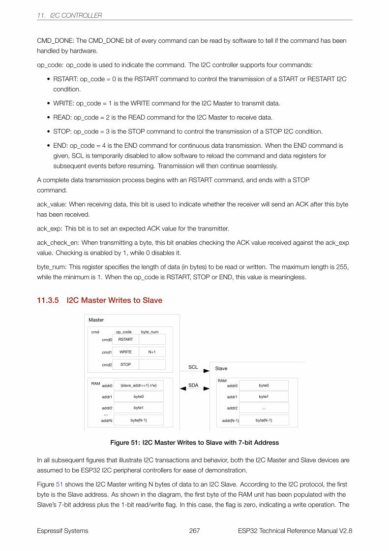
11. I2C CONTROLLER
CMD_DONE: The CMD_DONE bit of every command can be read by software to tell if the command has been
handled by hardware.
op_code: op_code is used to indicate the command. The I2C controller supports four commands:
• RSTART: op_code = 0 is the RSTART command to control the transmission of a START or RESTART I2C
condition.
• WRITE: op_code = 1 is the WRITE command for the I2C Master to transmit data.
• READ: op_code = 2 is the READ command for the I2C Master to receive data.
• STOP: op_code = 3 is the STOP command to control the transmission of a STOP I2C condition.
• END: op_code = 4 is the END command for continuous data transmission. When the END command is
given, SCL is temporarily disabled to allow software to reload the command and data registers for
subsequent events before resuming. Transmission will then continue seamlessly.
A complete data transmission process begins with an RSTART command, and ends with a STOP
command.
ack_value: When receiving data, this bit is used to indicate whether the receiver will send an ACK after this byte
has been received.
ack_exp: This bit is to set an expected ACK value for the transmitter.
ack_check_en: When transmitting a byte, this bit enables checking the ACK value received against the ack_exp
value. Checking is enabled by 1, while 0 disables it.
byte_num: This register specifies the length of data (in bytes) to be read or written. The maximum length is 255,
while the minimum is 1. When the op_code is RSTART, STOP or END, this value is meaningless.
11.3.5 I2C Master Writes to Slave
Figure 51: I2C Master Writes to Slave with 7-bit Address
In all subsequent figures that illustrate I2C transactions and behavior, both the I2C Master and Slave devices are
assumed to be ESP32 I2C peripheral controllers for ease of demonstration.
Figure 51 shows the I2C Master writing N bytes of data to an I2C Slave. According to the I2C protocol, the first
byte is the Slave address. As shown in the diagram, the first byte of the RAM unit has been populated with the
Slave’s 7-bit address plus the 1-bit read/write flag. In this case, the flag is zero, indicating a write operation. The
Espressif Systems 267 ESP32 Technical Reference Manual V2.8
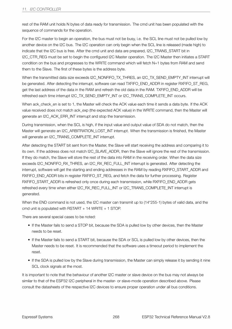
11. I2C CONTROLLER
rest of the RAM unit holds N bytes of data ready for transmission. The cmd unit has been populated with the
sequence of commands for the operation.
For the I2C master to begin an operation, the bus must not be busy, i.e. the SCL line must not be pulled low by
another device on the I2C bus. The I2C operation can only begin when the SCL line is released (made high) to
indicate that the I2C bus is free. After the cmd unit and data are prepared, I2C_TRANS_START bit in
I2C_CTR_REG must be set to begin the configured I2C Master operation. The I2C Master then initiates a START
condition on the bus and progresses to the WRITE command which will fetch N+1 bytes from RAM and send
them to the Slave. The first of these bytes is the address byte.
When the transmitted data size exceeds I2C_NONFIFO_TX_THRES, an I2C_TX_SEND_EMPTY_INT interrupt will
be generated. After detecting the interrupt, software can read TXFIFO_END_ADDR in register RXFIFO_ST_REG,
get the last address of the data in the RAM and refresh the old data in the RAM. TXFIFO_END_ADDR will be
refreshed each time interrupt I2C_TX_SEND_EMPTY_INT or I2C_TRANS_COMPLETE_INT occurs.
When ack_check_en is set to 1, the Master will check the ACK value each time it sends a data byte. If the ACK
value received does not match ack_exp (the expected ACK value) in the WRITE command, then the Master will
generate an I2C_ACK_ERR_INT interrupt and stop the transmission.
During transmission, when the SCL is high, if the input value and output value of SDA do not match, then the
Master will generate an I2C_ARBITRATION_LOST_INT interrupt. When the transmission is finished, the Master
will generate an I2C_TRANS_COMPLETE_INT interrupt.
After detecting the START bit sent from the Master, the Slave will start receiving the address and comparing it to
its own. If the address does not match I2C_SLAVE_ADDR, then the Slave will ignore the rest of the transmission.
If they do match, the Slave will store the rest of the data into RAM in the receiving order. When the data size
exceeds I2C_NONFIFO_RX_THRES, an I2C_RX_REC_FULL_INT interrupt is generated. After detecting the
interrupt, software will get the starting and ending addresses in the RAM by reading RXFIFO_START_ADDR and
RXFIFO_END_ADDR bits in register RXFIFO_ST_REG, and fetch the data for further processing. Register
RXFIFO_START_ADDR is refreshed only once during each transmission, while RXFIFO_END_ADDR gets
refreshed every time when either I2C_RX_REC_FULL_INT or I2C_TRANS_COMPLETE_INT interrupt is
generated.
When the END command is not used, the I2C master can transmit up to (14*255-1) bytes of valid data, and the
cmd unit is populated with RSTART + 14 WRITE + 1 STOP.
There are several special cases to be noted:
• If the Master fails to send a STOP bit, because the SDA is pulled low by other devices, then the Master
needs to be reset.
• If the Master fails to send a START bit, because the SDA or SCL is pulled low by other devices, then the
Master needs to be reset. It is recommended that the software uses a timeout period to implement the
reset.
• If the SDA is pulled low by the Slave during transmission, the Master can simply release it by sending it nine
SCL clock signals at the most.
It is important to note that the behaviour of another I2C master or slave device on the bus may not always be
similar to that of the ESP32 I2C peripheral in the master- or slave-mode operation described above. Please
consult the datasheets of the respective I2C devices to ensure proper operation under all bus conditions.
Espressif Systems 268 ESP32 Technical Reference Manual V2.8
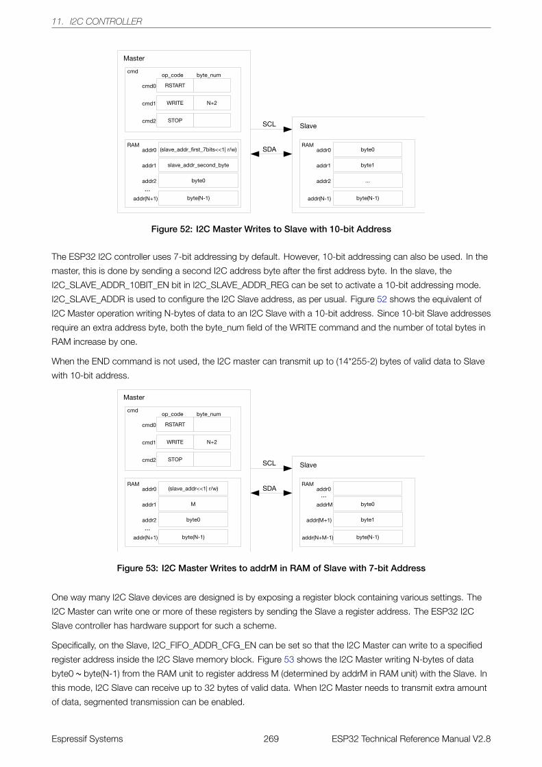
11. I2C CONTROLLER
Figure 52: I2C Master Writes to Slave with 10-bit Address
The ESP32 I2C controller uses 7-bit addressing by default. However, 10-bit addressing can also be used. In the
master, this is done by sending a second I2C address byte after the first address byte. In the slave, the
I2C_SLAVE_ADDR_10BIT_EN bit in I2C_SLAVE_ADDR_REG can be set to activate a 10-bit addressing mode.
I2C_SLAVE_ADDR is used to configure the I2C Slave address, as per usual. Figure 52 shows the equivalent of
I2C Master operation writing N-bytes of data to an I2C Slave with a 10-bit address. Since 10-bit Slave addresses
require an extra address byte, both the byte_num field of the WRITE command and the number of total bytes in
RAM increase by one.
When the END command is not used, the I2C master can transmit up to (14*255-2) bytes of valid data to Slave
with 10-bit address.
Figure 53: I2C Master Writes to addrM in RAM of Slave with 7-bit Address
One way many I2C Slave devices are designed is by exposing a register block containing various settings. The
I2C Master can write one or more of these registers by sending the Slave a register address. The ESP32 I2C
Slave controller has hardware support for such a scheme.
Specifically, on the Slave, I2C_FIFO_ADDR_CFG_EN can be set so that the I2C Master can write to a specified
register address inside the I2C Slave memory block. Figure 53 shows the I2C Master writing N-bytes of data
byte0 ~ byte(N-1) from the RAM unit to register address M (determined by addrM in RAM unit) with the Slave. In
this mode, I2C Slave can receive up to 32 bytes of valid data. When I2C Master needs to transmit extra amount
of data, segmented transmission can be enabled.
Espressif Systems 269 ESP32 Technical Reference Manual V2.8
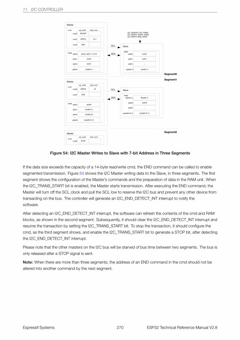
11. I2C CONTROLLER
Figure 54: I2C Master Writes to Slave with 7-bit Address in Three Segments
If the data size exceeds the capacity of a 14-byte read/write cmd, the END command can be called to enable
segmented transmission. Figure 54 shows the I2C Master writing data to the Slave, in three segments. The first
segment shows the configuration of the Master’s commands and the preparation of data in the RAM unit. When
the I2C_TRANS_START bit is enabled, the Master starts transmission. After executing the END command, the
Master will turn off the SCL clock and pull the SCL low to reserve the I2C bus and prevent any other device from
transacting on the bus. The controller will generate an I2C_END_DETECT_INT interrupt to notify the
software.
After detecting an I2C_END_DETECT_INT interrupt, the software can refresh the contents of the cmd and RAM
blocks, as shown in the second segment. Subsequently, it should clear the I2C_END_DETECT_INT interrupt and
resume the transaction by setting the I2C_TRANS_START bit. To stop the transaction, it should configure the
cmd, as the third segment shows, and enable the I2C_TRANS_START bit to generate a STOP bit, after detecting
the I2C_END_DETECT_INT interrupt.
Please note that the other masters on the I2C bus will be starved of bus time between two segments. The bus is
only released after a STOP signal is sent.
Note: When there are more than three segments, the address of an END command in the cmd should not be
altered into another command by the next segment.
Espressif Systems 270 ESP32 Technical Reference Manual V2.8
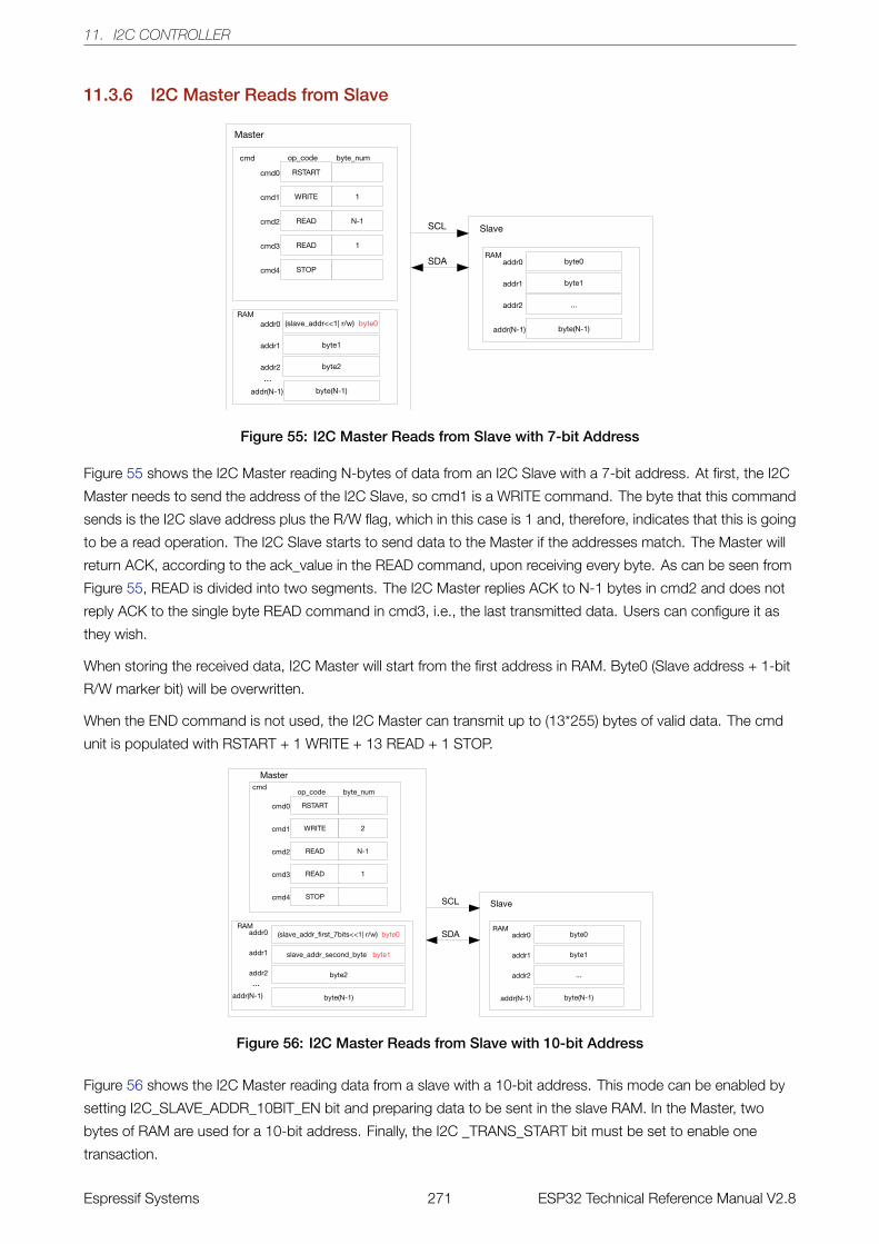
11. I2C CONTROLLER
11.3.6 I2C Master Reads from Slave
Figure 55: I2C Master Reads from Slave with 7-bit Address
Figure 55 shows the I2C Master reading N-bytes of data from an I2C Slave with a 7-bit address. At first, the I2C
Master needs to send the address of the I2C Slave, so cmd1 is a WRITE command. The byte that this command
sends is the I2C slave address plus the R/W flag, which in this case is 1 and, therefore, indicates that this is going
to be a read operation. The I2C Slave starts to send data to the Master if the addresses match. The Master will
return ACK, according to the ack_value in the READ command, upon receiving every byte. As can be seen from
Figure 55, READ is divided into two segments. The I2C Master replies ACK to N-1 bytes in cmd2 and does not
reply ACK to the single byte READ command in cmd3, i.e., the last transmitted data. Users can configure it as
they wish.
When storing the received data, I2C Master will start from the first address in RAM. Byte0 (Slave address + 1-bit
R/W marker bit) will be overwritten.
When the END command is not used, the I2C Master can transmit up to (13*255) bytes of valid data. The cmd
unit is populated with RSTART + 1 WRITE + 13 READ + 1 STOP.
Figure 56: I2C Master Reads from Slave with 10-bit Address
Figure 56 shows the I2C Master reading data from a slave with a 10-bit address. This mode can be enabled by
setting I2C_SLAVE_ADDR_10BIT_EN bit and preparing data to be sent in the slave RAM. In the Master, two
bytes of RAM are used for a 10-bit address. Finally, the I2C _TRANS_START bit must be set to enable one
transaction.
Espressif Systems 271 ESP32 Technical Reference Manual V2.8
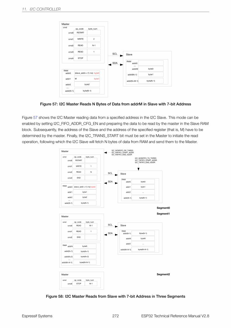
11. I2C CONTROLLER
Figure 57: I2C Master Reads N Bytes of Data from addrM in Slave with 7-bit Address
Figure 57 shows the I2C Master reading data from a specified address in the I2C Slave. This mode can be
enabled by setting I2C_FIFO_ADDR_CFG_EN and preparing the data to be read by the master in the Slave RAM
block. Subsequently, the address of the Slave and the address of the specified register (that is, M) have to be
determined by the master. Finally, the I2C_TRANS_START bit must be set in the Master to initiate the read
operation, following which the I2C Slave will fetch N bytes of data from RAM and send them to the Master.
Figure 58: I2C Master Reads from Slave with 7-bit Address in Three Segments
Espressif Systems 272 ESP32 Technical Reference Manual V2.8
11. I2C CONTROLLER
Figure 58 shows the I2C Master reading N+M bytes of data in three segments from the I2C Slave. The first
segment shows the configuration of the cmd and the preparation of data in the Slave RAM. When the
I2C_TRANS_START bit is enabled, the I2C Master starts the operation. The I2C Master will refresh the cmd after
executing the END command. It will clear the I2C_END_DETECT_INT interrupt, set the I2C_TRANS_START bit
and resume the transaction. To stop the transaction, the I2C Master will configure the cmd, as the third segment
shows, after detecting the I2C_END_DETECT_INT interrupt. After setting the I2C_TRANS_START bit, I2C Master
will send a STOP bit to stop the transaction.
11.3.7 Interrupts
• I2C_TX_SEND_EMPTY_INT: Triggered when the I2C has sent nonfifo_tx_thres bytes of data.
• I2C_RX_REC_FULL_INT: Triggered when the I2C has received nonfifo_rx_thres bytes of data.
• I2C_ACK_ERR_INT: Triggered when the I2C Master receives an ACK that is not as expected, or when the
I2C Slave receives an ACK whose value is 1.
• I2C_TRANS_START_INT: Triggered when the I2C sends the START bit.
• I2C_TIME_OUT_INT: Triggered when the SCL stays high or low for more than I2C_TIME_OUT clocks.
• I2C_TRANS_COMPLETE_INT: Triggered when the I2C detects a STOP bit.
• I2C_MASTER_TRAN_COMP_INT: Triggered when the I2C Master sends or receives a byte.
• I2C_ARBITRATION_LOST_INT: Triggered when the I2C Master’s SCL is high, while the output value and
input value of the SDA do not match.
• I2C_SLAVE_TRAN_COMP_INT: Triggered when the I2C Slave detects a STOP bit.
• I2C_END_DETECT_INT: Triggered when the I2C deals with the END command.
Espressif Systems 273 ESP32 Technical Reference Manual V2.8
11. I2C CONTROLLER
11.4 Register Summary
Name Description I2C0 I2C1 Acc
Configuration registers
I2C_SLAVE_ADDR_REG Configures the I2C slave address 0x3FF53010 0x3FF67010 R/W
I2C_RXFIFO_ST_REG FIFO status register 0x3FF53014 0x3FF67014 RO
I2C_FIFO_CONF_REG FIFO configuration register 0x3FF53018 0x3FF67018 R/W
Timing registers
I2C_SDA_HOLD_REGConfigures the hold time after a negative
SCL edge0x3FF53030 0x3FF67030 R/W
I2C_SDA_SAMPLE_REGConfigures the sample time after a positive
SCL edge0x3FF53034 0x3FF67034 R/W
I2C_SCL_LOW_PERIOD_REGConfigures the low level width of the SCL
clock0x3FF53000 0x3FF67000 R/W
I2C_SCL_HIGH_PERIOD_REGConfigures the high level width of the SCL
clock0x3FF53038 0x3FF67038 R/W
I2C_SCL_START_HOLD_REGConfigures the delay between the SDA and
SCL negative edge for a start condition0x3FF53040 0x3FF67040 R/W
I2C_SCL_RSTART_SETUP_REGConfigures the delay between the positive
edge of SCL and the negative edge of SDA0x3FF53044 0x3FF67044 R/W
I2C_SCL_STOP_HOLD_REGConfigures the delay after the SCL clock
edge for a stop condition0x3FF53048 0x3FF67048 R/W
I2C_SCL_STOP_SETUP_REGConfigures the delay between the SDA and
SCL positive edge for a stop condition0x3FF5304C 0x3FF6704C R/W
Filter registers
I2C_SCL_FILTER_CFG_REG SCL filter configuration register 0x3FF53050 0x3FF67050 R/W
I2C_SDA_FILTER_CFG_REG SDA filter configuration register 0x3FF53054 0x3FF67054 R/W
Interrupt registers
I2C_INT_RAW_REG Raw interrupt status 0x3FF53020 0x3FF67020 RO
I2C_INT_ENA_REG Interrupt enable bits 0x3FF53028 0x3FF67028 R/W
I2C_INT_CLR_REG Interrupt clear bits 0x3FF53024 0x3FF67024 WO
Command registers
I2C_COMD0_REG I2C command register 0 0x3FF53058 0x3FF67058 R/W
I2C_COMD1_REG I2C command register 1 0x3FF5305C 0x3FF6705C R/W
I2C_COMD2_REG I2C command register 2 0x3FF53060 0x3FF67060 R/W
I2C_COMD3_REG I2C command register 3 0x3FF53064 0x3FF67064 R/W
I2C_COMD4_REG I2C command register 4 0x3FF53068 0x3FF67068 R/W
I2C_COMD5_REG I2C command register 5 0x3FF5306C 0x3FF6706C R/W
I2C_COMD6_REG I2C command register 6 0x3FF53070 0x3FF67070 R/W
I2C_COMD7_REG I2C command register 7 0x3FF53074 0x3FF67074 R/W
I2C_COMD8_REG I2C command register 8 0x3FF53078 0x3FF67078 R/W
I2C_COMD9_REG I2C command register 9 0x3FF5307C 0x3FF6707C R/W
I2C_COMD10_REG I2C command register 10 0x3FF53080 0x3FF67080 R/W
I2C_COMD11_REG I2C command register 11 0x3FF53084 0x3FF67084 R/W
I2C_COMD12_REG I2C command register 12 0x3FF53088 0x3FF67088 R/W
Espressif Systems 274 ESP32 Technical Reference Manual V2.8
11. I2C CONTROLLER
Name Description I2C0 I2C1 Acc
I2C_COMD13_REG I2C command register 13 0x3FF5308C 0x3FF6708C R/W
I2C_COMD14_REG I2C command register 14 0x3FF53090 0x3FF67090 R/W
I2C_COMD15_REG I2C command register 15 0x3FF53094 0x3FF67094 R/W
Espressif Systems 275 ESP32 Technical Reference Manual V2.8
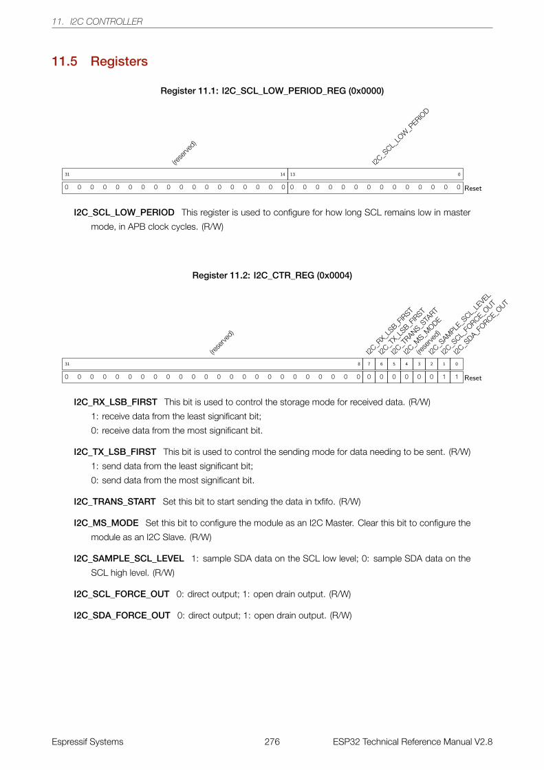
11. I2C CONTROLLER
11.5 Registers
Register 11.1: I2C_SCL_LOW_PERIOD_REG (0x0000)
(rese
rved)
0 0 0 0 0 0 0 0 0 0 0 0 0 0 0 0 0 0
31 14
I2C_S
CL_LO
W_P
ERIOD
0 0 0 0 0 0 0 0 0 0 0 0 0 0
13 0
Reset
I2C_SCL_LOW_PERIOD This register is used to configure for how long SCL remains low in master
mode, in APB clock cycles. (R/W)
Register 11.2: I2C_CTR_REG (0x0004)
(rese
rved)
0 0 0 0 0 0 0 0 0 0 0 0 0 0 0 0 0 0 0 0 0 0 0 0
31 8
I2C_R
X_LS
B_FIR
ST
0
7
I2C_T
X_LS
B_FIR
ST
0
6
I2C_T
RANS_STA
RT
0
5
I2C_M
S_MODE
0
4
(rese
rved)
0
3
I2C_S
AMPLE
_SCL_
LEVEL
0
2
I2C_S
CL_FO
RCE_OUT
1
1
I2C_S
DA_FORCE_O
UT
1
0
Reset
I2C_RX_LSB_FIRST This bit is used to control the storage mode for received data. (R/W)
1: receive data from the least significant bit;
0: receive data from the most significant bit.
I2C_TX_LSB_FIRST This bit is used to control the sending mode for data needing to be sent. (R/W)
1: send data from the least significant bit;
0: send data from the most significant bit.
I2C_TRANS_START Set this bit to start sending the data in txfifo. (R/W)
I2C_MS_MODE Set this bit to configure the module as an I2C Master. Clear this bit to configure the
module as an I2C Slave. (R/W)
I2C_SAMPLE_SCL_LEVEL 1: sample SDA data on the SCL low level; 0: sample SDA data on the
SCL high level. (R/W)
I2C_SCL_FORCE_OUT 0: direct output; 1: open drain output. (R/W)
I2C_SDA_FORCE_OUT 0: direct output; 1: open drain output. (R/W)
Espressif Systems 276 ESP32 Technical Reference Manual V2.8
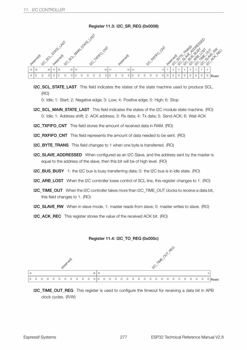
11. I2C CONTROLLER
Register 11.3: I2C_SR_REG (0x0008)
(rese
rved)
0
31
I2C_S
CL_STA
TE_L
AST
0 0 0
30 28
(rese
rved)
0
27
I2C_S
CL_M
AIN_S
TATE
_LAST
0 0 0
26 24
I2C_T
XFIFO
_CNT
0 0 0 0 0 0
23 18
(rese
rved)
0 0 0 0
17 14
I2C_R
XFIFO
_CNT
0 0 0 0 0 0
13 8
(rese
rved)
0
7
I2C_B
YTE_T
RANS
0
6
I2C_S
LAVE_A
DDRESSED
0
5
I2C_B
US_BUSY
0
4
I2C_A
RB_LOST
0
3
I2C_T
IME_O
UT
0
2
I2C_S
LAVE_R
W
0
1
I2C_A
CK_REC
0
0
Reset
I2C_SCL_STATE_LAST This field indicates the states of the state machine used to produce SCL.
(RO)
0: Idle; 1: Start; 2: Negative edge; 3: Low; 4: Positive edge; 5: High; 6: Stop
I2C_SCL_MAIN_STATE_LAST This field indicates the states of the I2C module state machine. (RO)
0: Idle; 1: Address shift; 2: ACK address; 3: Rx data; 4: Tx data; 5: Send ACK; 6: Wait ACK
I2C_TXFIFO_CNT This field stores the amount of received data in RAM. (RO)
I2C_RXFIFO_CNT This field represents the amount of data needed to be sent. (RO)
I2C_BYTE_TRANS This field changes to 1 when one byte is transferred. (RO)
I2C_SLAVE_ADDRESSED When configured as an I2C Slave, and the address sent by the master is
equal to the address of the slave, then this bit will be of high level. (RO)
I2C_BUS_BUSY 1: the I2C bus is busy transferring data; 0: the I2C bus is in idle state. (RO)
I2C_ARB_LOST When the I2C controller loses control of SCL line, this register changes to 1. (RO)
I2C_TIME_OUT When the I2C controller takes more than I2C_TIME_OUT clocks to receive a data bit,
this field changes to 1. (RO)
I2C_SLAVE_RW When in slave mode, 1: master reads from slave; 0: master writes to slave. (RO)
I2C_ACK_REC This register stores the value of the received ACK bit. (RO)
Register 11.4: I2C_TO_REG (0x000c)
(rese
rved)
0 0 0 0 0 0 0 0 0 0 0 0
31 20
I2C_T
IME_O
UT_REG
0 0 0 0 0 0 0 0 0 0 0 0 0 0 0 0 0 0 0 0
19 0
Reset
I2C_TIME_OUT_REG This register is used to configure the timeout for receiving a data bit in APB
clock cycles. (R/W)
Espressif Systems 277 ESP32 Technical Reference Manual V2.8
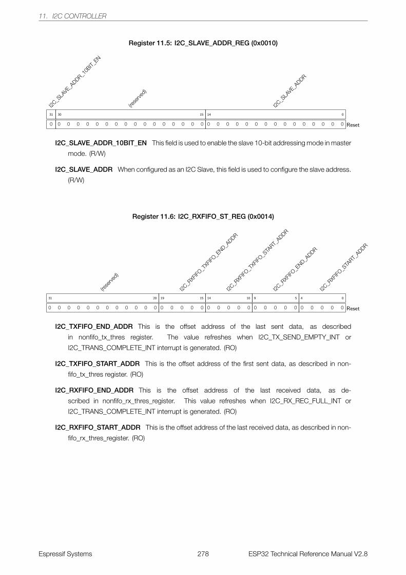
11. I2C CONTROLLER
Register 11.5: I2C_SLAVE_ADDR_REG (0x0010)
I2C_S
LAVE_A
DDR_10B
IT_EN
0
31
(rese
rved)
0 0 0 0 0 0 0 0 0 0 0 0 0 0 0 0
30 15
I2C_S
LAVE_A
DDR
0 0 0 0 0 0 0 0 0 0 0 0 0 0 0
14 0
Reset
I2C_SLAVE_ADDR_10BIT_EN This field is used to enable the slave 10-bit addressing mode in master
mode. (R/W)
I2C_SLAVE_ADDR When configured as an I2C Slave, this field is used to configure the slave address.
(R/W)
Register 11.6: I2C_RXFIFO_ST_REG (0x0014)
(rese
rved)
0 0 0 0 0 0 0 0 0 0 0 0
31 20
I2C_R
XFIFO
_TXF
IFO_E
ND_ADDR
0 0 0 0 0
19 15
I2C_R
XFIFO
_TXF
IFO_S
TART_
ADDR
0 0 0 0 0
14 10
I2C_R
XFIFO
_END_A
DDR
0 0 0 0 0
9 5
I2C_R
XFIFO
_STA
RT_ADDR
0 0 0 0 0
4 0
Reset
I2C_TXFIFO_END_ADDR This is the offset address of the last sent data, as described
in nonfifo_tx_thres register. The value refreshes when I2C_TX_SEND_EMPTY_INT or
I2C_TRANS_COMPLETE_INT interrupt is generated. (RO)
I2C_TXFIFO_START_ADDR This is the offset address of the first sent data, as described in non-
fifo_tx_thres register. (RO)
I2C_RXFIFO_END_ADDR This is the offset address of the last received data, as de-
scribed in nonfifo_rx_thres_register. This value refreshes when I2C_RX_REC_FULL_INT or
I2C_TRANS_COMPLETE_INT interrupt is generated. (RO)
I2C_RXFIFO_START_ADDR This is the offset address of the last received data, as described in non-
fifo_rx_thres_register. (RO)
Espressif Systems 278 ESP32 Technical Reference Manual V2.8
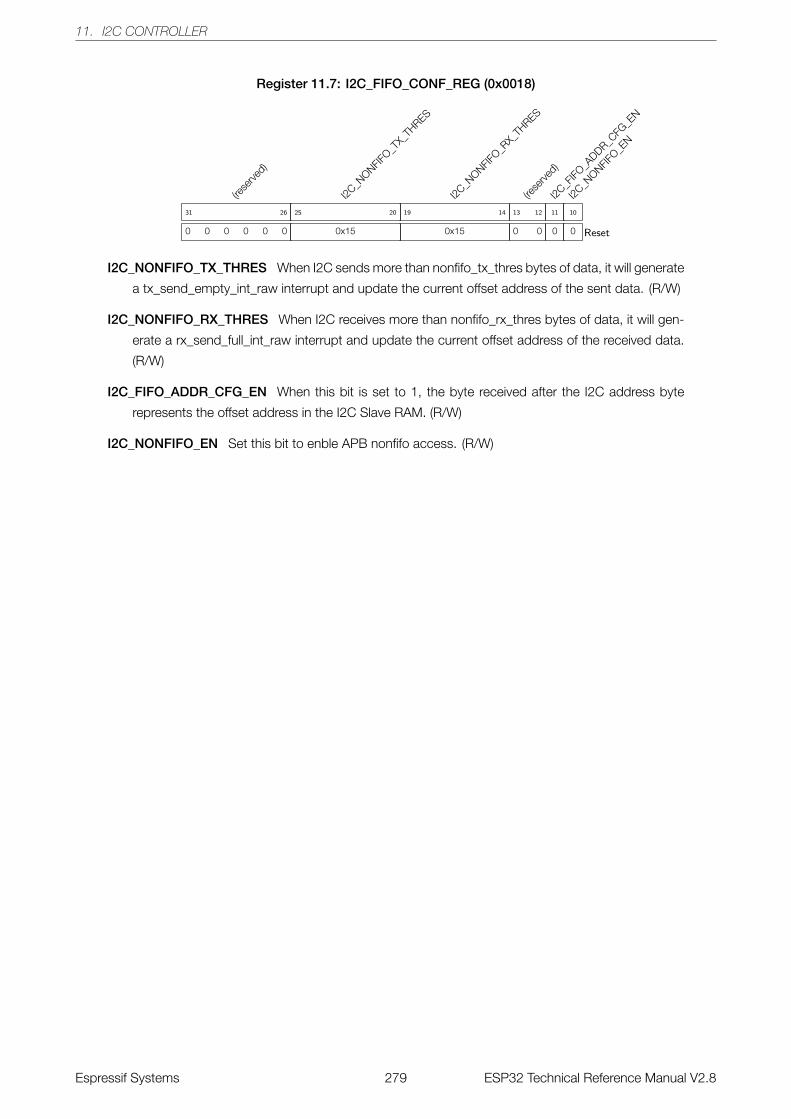
11. I2C CONTROLLER
Register 11.7: I2C_FIFO_CONF_REG (0x0018)
(rese
rved)
0 0 0 0 0 0
31 26
I2C_N
ONFIFO_T
X_TH
RES
0x15
25 20
I2C_N
ONFIFO_R
X_TH
RES
0x15
19 14
(rese
rved)
0 0
13 12
I2C_F
IFO_A
DDR_CFG
_EN
0
11
I2C_N
ONFIFO_E
N
0
10
Reset
I2C_NONFIFO_TX_THRES When I2C sends more than nonfifo_tx_thres bytes of data, it will generate
a tx_send_empty_int_raw interrupt and update the current offset address of the sent data. (R/W)
I2C_NONFIFO_RX_THRES When I2C receives more than nonfifo_rx_thres bytes of data, it will gen-
erate a rx_send_full_int_raw interrupt and update the current offset address of the received data.
(R/W)
I2C_FIFO_ADDR_CFG_EN When this bit is set to 1, the byte received after the I2C address byte
represents the offset address in the I2C Slave RAM. (R/W)
I2C_NONFIFO_EN Set this bit to enble APB nonfifo access. (R/W)
Espressif Systems 279 ESP32 Technical Reference Manual V2.8
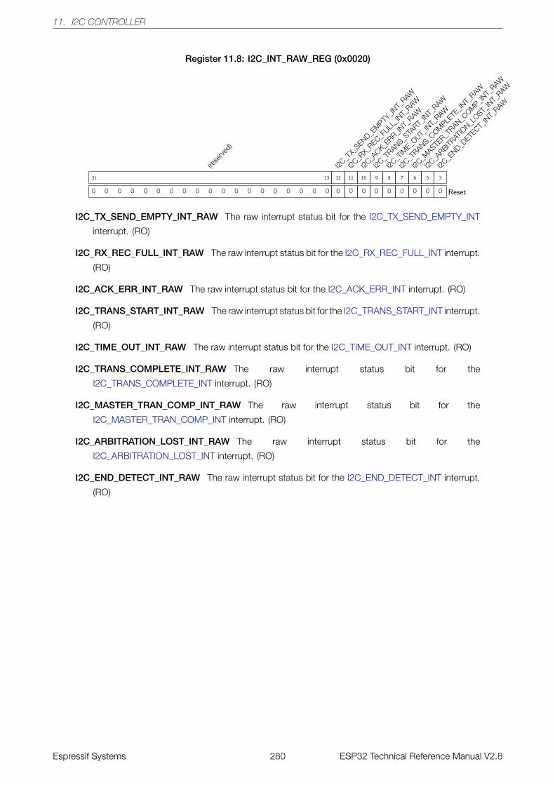
11. I2C CONTROLLER
Register 11.8: I2C_INT_RAW_REG (0x0020)
(rese
rved)
0 0 0 0 0 0 0 0 0 0 0 0 0 0 0 0 0 0 0
31 13
I2C_T
X_SEND_E
MPTY
_INT_
RAW
0
12
I2C_R
X_REC_F
ULL_IN
T_RAW
0
11
I2C_A
CK_ERR_IN
T_RAW
0
10
I2C_T
RANS_STA
RT_IN
T_RAW
0
9
I2C_T
IME_O
UT_IN
T_RAW
0
8
I2C_T
RANS_COM
PLETE
_INT_
RAW
0
7
I2C_M
ASTER_T
RAN_COM
P_INT_
RAW
0
6
I2C_A
RBITRAT
ION_L
OST_IN
T_RAW
0
5
I2C_E
ND_DETE
CT_IN
T_RAW
0
3
Reset
I2C_TX_SEND_EMPTY_INT_RAW The raw interrupt status bit for the I2C_TX_SEND_EMPTY_INT
interrupt. (RO)
I2C_RX_REC_FULL_INT_RAW The raw interrupt status bit for the I2C_RX_REC_FULL_INT interrupt.
(RO)
I2C_ACK_ERR_INT_RAW The raw interrupt status bit for the I2C_ACK_ERR_INT interrupt. (RO)
I2C_TRANS_START_INT_RAW The raw interrupt status bit for the I2C_TRANS_START_INT interrupt.
(RO)
I2C_TIME_OUT_INT_RAW The raw interrupt status bit for the I2C_TIME_OUT_INT interrupt. (RO)
I2C_TRANS_COMPLETE_INT_RAW The raw interrupt status bit for the
I2C_TRANS_COMPLETE_INT interrupt. (RO)
I2C_MASTER_TRAN_COMP_INT_RAW The raw interrupt status bit for the
I2C_MASTER_TRAN_COMP_INT interrupt. (RO)
I2C_ARBITRATION_LOST_INT_RAW The raw interrupt status bit for the
I2C_ARBITRATION_LOST_INT interrupt. (RO)
I2C_END_DETECT_INT_RAW The raw interrupt status bit for the I2C_END_DETECT_INT interrupt.
(RO)
Espressif Systems 280 ESP32 Technical Reference Manual V2.8
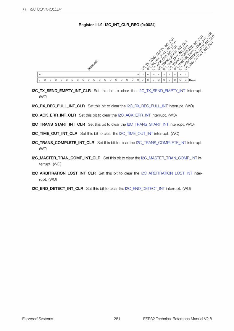
11. I2C CONTROLLER
Register 11.9: I2C_INT_CLR_REG (0x0024)
(rese
rved)
0 0 0 0 0 0 0 0 0 0 0 0 0 0 0 0 0 0 0
31 13
I2C_T
X_SEND_E
MPTY
_INT_
CLR
0
12
I2C_R
X_REC_F
ULL_IN
T_CLR
0
11
I2C_A
CK_ERR_IN
T_CLR
0
10
I2C_T
RANS_STA
RT_IN
T_CLR
0
9
I2C_T
IME_O
UT_IN
T_CLR
0
8
I2C_T
RANS_COM
PLETE
_INT_
CLR
0
7
I2C_M
ASTER_T
RAN_COM
P_INT_
CLR
0
6
I2C_A
RBITRAT
ION_L
OST_IN
T_CLR
0
5
I2C_E
ND_DETE
CT_IN
T_CLR
0
3
Reset
I2C_TX_SEND_EMPTY_INT_CLR Set this bit to clear the I2C_TX_SEND_EMPTY_INT interrupt.
(WO)
I2C_RX_REC_FULL_INT_CLR Set this bit to clear the I2C_RX_REC_FULL_INT interrupt. (WO)
I2C_ACK_ERR_INT_CLR Set this bit to clear the I2C_ACK_ERR_INT interrupt. (WO)
I2C_TRANS_START_INT_CLR Set this bit to clear the I2C_TRANS_START_INT interrupt. (WO)
I2C_TIME_OUT_INT_CLR Set this bit to clear the I2C_TIME_OUT_INT interrupt. (WO)
I2C_TRANS_COMPLETE_INT_CLR Set this bit to clear the I2C_TRANS_COMPLETE_INT interrupt.
(WO)
I2C_MASTER_TRAN_COMP_INT_CLR Set this bit to clear the I2C_MASTER_TRAN_COMP_INT in-
terrupt. (WO)
I2C_ARBITRATION_LOST_INT_CLR Set this bit to clear the I2C_ARBITRATION_LOST_INT inter-
rupt. (WO)
I2C_END_DETECT_INT_CLR Set this bit to clear the I2C_END_DETECT_INT interrupt. (WO)
Espressif Systems 281 ESP32 Technical Reference Manual V2.8
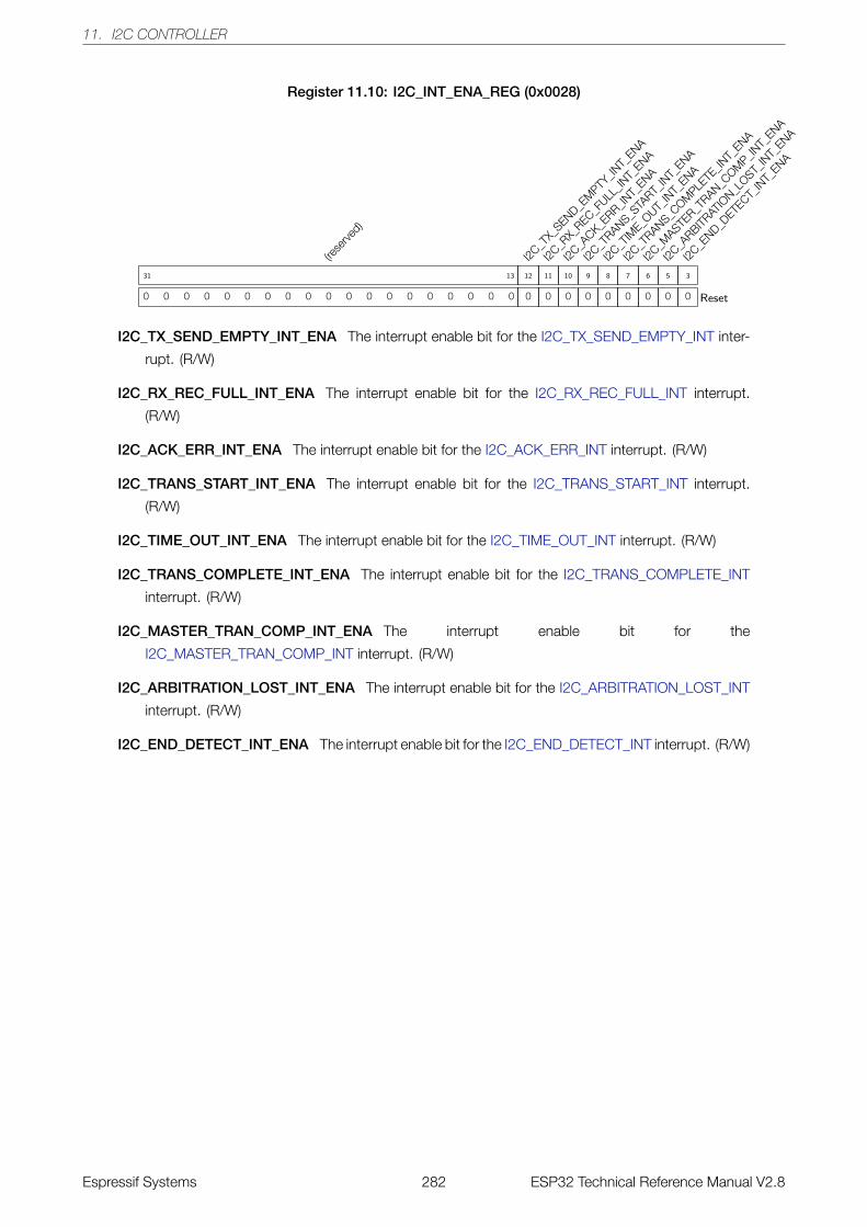
11. I2C CONTROLLER
Register 11.10: I2C_INT_ENA_REG (0x0028)
(rese
rved)
0 0 0 0 0 0 0 0 0 0 0 0 0 0 0 0 0 0 0
31 13
I2C_T
X_SEND_E
MPTY
_INT_
ENA
0
12
I2C_R
X_REC_F
ULL_IN
T_ENA
0
11
I2C_A
CK_ERR_IN
T_ENA
0
10
I2C_T
RANS_STA
RT_IN
T_ENA
0
9
I2C_T
IME_O
UT_IN
T_ENA
0
8
I2C_T
RANS_COM
PLETE
_INT_
ENA
0
7
I2C_M
ASTER_T
RAN_COM
P_INT_
ENA
0
6
I2C_A
RBITRAT
ION_L
OST_IN
T_ENA
0
5
I2C_E
ND_DETE
CT_IN
T_ENA
0
3
Reset
I2C_TX_SEND_EMPTY_INT_ENA The interrupt enable bit for the I2C_TX_SEND_EMPTY_INT inter-
rupt. (R/W)
I2C_RX_REC_FULL_INT_ENA The interrupt enable bit for the I2C_RX_REC_FULL_INT interrupt.
(R/W)
I2C_ACK_ERR_INT_ENA The interrupt enable bit for the I2C_ACK_ERR_INT interrupt. (R/W)
I2C_TRANS_START_INT_ENA The interrupt enable bit for the I2C_TRANS_START_INT interrupt.
(R/W)
I2C_TIME_OUT_INT_ENA The interrupt enable bit for the I2C_TIME_OUT_INT interrupt. (R/W)
I2C_TRANS_COMPLETE_INT_ENA The interrupt enable bit for the I2C_TRANS_COMPLETE_INT
interrupt. (R/W)
I2C_MASTER_TRAN_COMP_INT_ENA The interrupt enable bit for the
I2C_MASTER_TRAN_COMP_INT interrupt. (R/W)
I2C_ARBITRATION_LOST_INT_ENA The interrupt enable bit for the I2C_ARBITRATION_LOST_INT
interrupt. (R/W)
I2C_END_DETECT_INT_ENA The interrupt enable bit for the I2C_END_DETECT_INT interrupt. (R/W)
Espressif Systems 282 ESP32 Technical Reference Manual V2.8
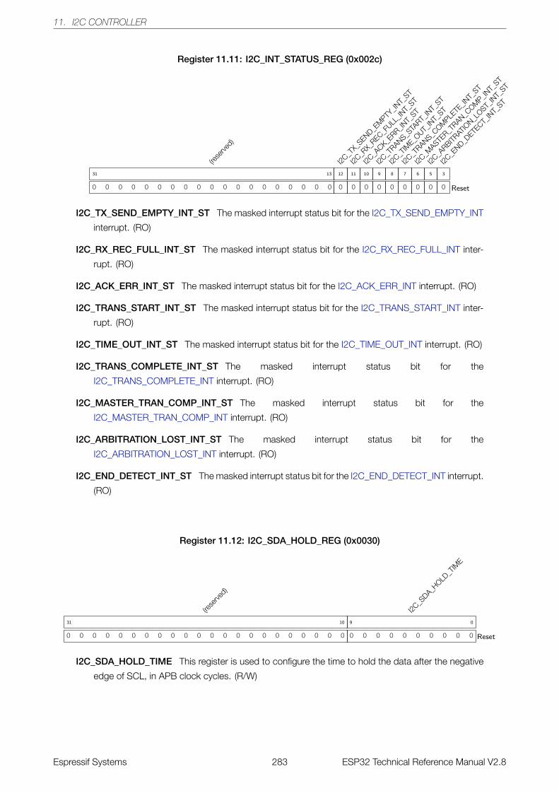
11. I2C CONTROLLER
Register 11.11: I2C_INT_STATUS_REG (0x002c)
(rese
rved)
0 0 0 0 0 0 0 0 0 0 0 0 0 0 0 0 0 0 0
31 13
I2C_T
X_SEND_E
MPTY
_INT_
ST
0
12
I2C_R
X_REC_F
ULL_IN
T_ST
0
11
I2C_A
CK_ERR_IN
T_ST
0
10
I2C_T
RANS_STA
RT_IN
T_ST
0
9
I2C_T
IME_O
UT_IN
T_ST
0
8
I2C_T
RANS_COM
PLETE
_INT_
ST
0
7
I2C_M
ASTER_T
RAN_COM
P_INT_
ST
0
6
I2C_A
RBITRAT
ION_L
OST_IN
T_ST
0
5
I2C_E
ND_DETE
CT_IN
T_ST
0
3
Reset
I2C_TX_SEND_EMPTY_INT_ST The masked interrupt status bit for the I2C_TX_SEND_EMPTY_INT
interrupt. (RO)
I2C_RX_REC_FULL_INT_ST The masked interrupt status bit for the I2C_RX_REC_FULL_INT inter-
rupt. (RO)
I2C_ACK_ERR_INT_ST The masked interrupt status bit for the I2C_ACK_ERR_INT interrupt. (RO)
I2C_TRANS_START_INT_ST The masked interrupt status bit for the I2C_TRANS_START_INT inter-
rupt. (RO)
I2C_TIME_OUT_INT_ST The masked interrupt status bit for the I2C_TIME_OUT_INT interrupt. (RO)
I2C_TRANS_COMPLETE_INT_ST The masked interrupt status bit for the
I2C_TRANS_COMPLETE_INT interrupt. (RO)
I2C_MASTER_TRAN_COMP_INT_ST The masked interrupt status bit for the
I2C_MASTER_TRAN_COMP_INT interrupt. (RO)
I2C_ARBITRATION_LOST_INT_ST The masked interrupt status bit for the
I2C_ARBITRATION_LOST_INT interrupt. (RO)
I2C_END_DETECT_INT_ST The masked interrupt status bit for the I2C_END_DETECT_INT interrupt.
(RO)
Register 11.12: I2C_SDA_HOLD_REG (0x0030)
(rese
rved)
0 0 0 0 0 0 0 0 0 0 0 0 0 0 0 0 0 0 0 0 0 0
31 10
I2C_S
DA_HOLD
_TIM
E
0 0 0 0 0 0 0 0 0 0
9 0
Reset
I2C_SDA_HOLD_TIME This register is used to configure the time to hold the data after the negative
edge of SCL, in APB clock cycles. (R/W)
Espressif Systems 283 ESP32 Technical Reference Manual V2.8
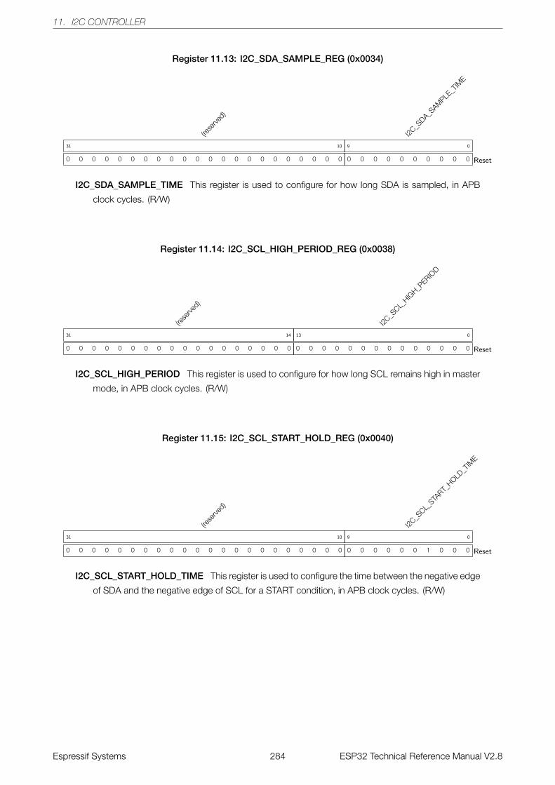
11. I2C CONTROLLER
Register 11.13: I2C_SDA_SAMPLE_REG (0x0034)
(rese
rved)
0 0 0 0 0 0 0 0 0 0 0 0 0 0 0 0 0 0 0 0 0 0
31 10
I2C_S
DA_SAM
PLE_T
IME
0 0 0 0 0 0 0 0 0 0
9 0
Reset
I2C_SDA_SAMPLE_TIME This register is used to configure for how long SDA is sampled, in APB
clock cycles. (R/W)
Register 11.14: I2C_SCL_HIGH_PERIOD_REG (0x0038)
(rese
rved)
0 0 0 0 0 0 0 0 0 0 0 0 0 0 0 0 0 0
31 14
I2C_S
CL_HIG
H_PERIO
D
0 0 0 0 0 0 0 0 0 0 0 0 0 0
13 0
Reset
I2C_SCL_HIGH_PERIOD This register is used to configure for how long SCL remains high in master
mode, in APB clock cycles. (R/W)
Register 11.15: I2C_SCL_START_HOLD_REG (0x0040)
(rese
rved)
0 0 0 0 0 0 0 0 0 0 0 0 0 0 0 0 0 0 0 0 0 0
31 10
I2C_S
CL_STA
RT_HOLD
_TIM
E
0 0 0 0 0 0 1 0 0 0
9 0
Reset
I2C_SCL_START_HOLD_TIME This register is used to configure the time between the negative edge
of SDA and the negative edge of SCL for a START condition, in APB clock cycles. (R/W)
Espressif Systems 284 ESP32 Technical Reference Manual V2.8
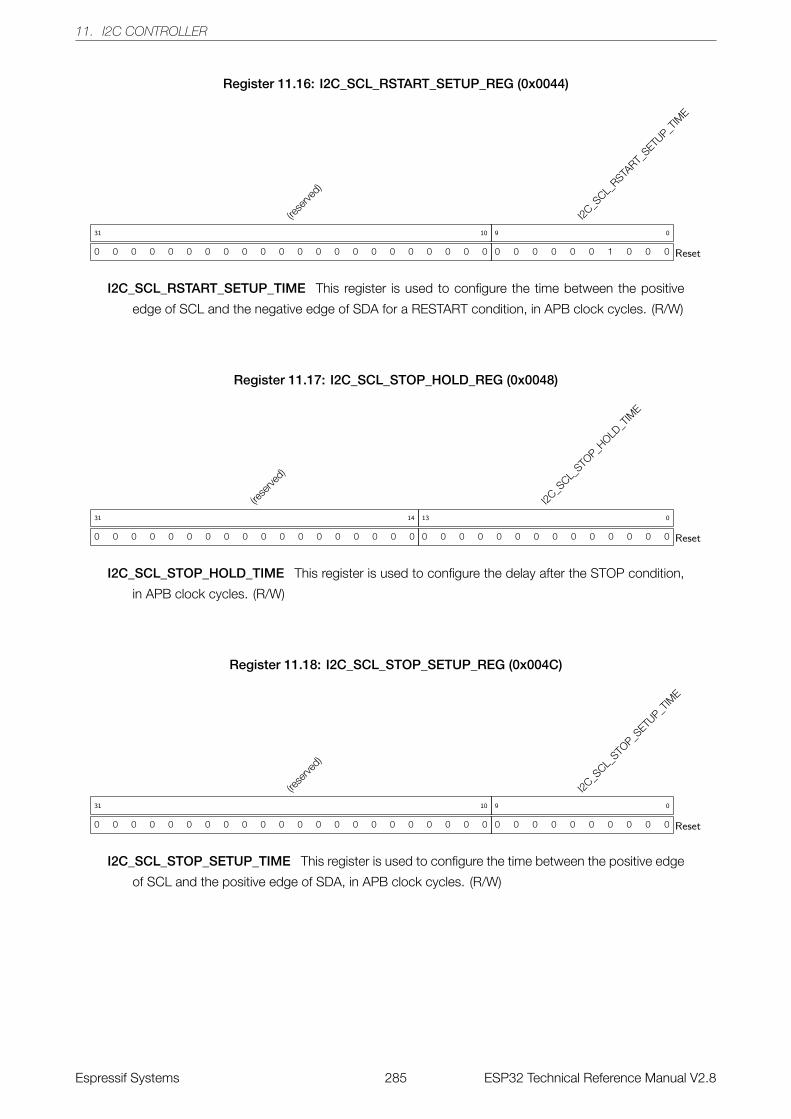
11. I2C CONTROLLER
Register 11.16: I2C_SCL_RSTART_SETUP_REG (0x0044)
(rese
rved)
0 0 0 0 0 0 0 0 0 0 0 0 0 0 0 0 0 0 0 0 0 0
31 10
I2C_S
CL_RSTA
RT_SETU
P_TIM
E
0 0 0 0 0 0 1 0 0 0
9 0
Reset
I2C_SCL_RSTART_SETUP_TIME This register is used to configure the time between the positive
edge of SCL and the negative edge of SDA for a RESTART condition, in APB clock cycles. (R/W)
Register 11.17: I2C_SCL_STOP_HOLD_REG (0x0048)
(rese
rved)
0 0 0 0 0 0 0 0 0 0 0 0 0 0 0 0 0 0
31 14
I2C_S
CL_STO
P_HOLD
_TIM
E
0 0 0 0 0 0 0 0 0 0 0 0 0 0
13 0
Reset
I2C_SCL_STOP_HOLD_TIME This register is used to configure the delay after the STOP condition,
in APB clock cycles. (R/W)
Register 11.18: I2C_SCL_STOP_SETUP_REG (0x004C)
(rese
rved)
0 0 0 0 0 0 0 0 0 0 0 0 0 0 0 0 0 0 0 0 0 0
31 10
I2C_S
CL_STO
P_SETU
P_TIM
E
0 0 0 0 0 0 0 0 0 0
9 0
Reset
I2C_SCL_STOP_SETUP_TIME This register is used to configure the time between the positive edge
of SCL and the positive edge of SDA, in APB clock cycles. (R/W)
Espressif Systems 285 ESP32 Technical Reference Manual V2.8
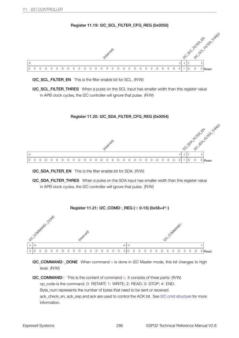
11. I2C CONTROLLER
Register 11.19: I2C_SCL_FILTER_CFG_REG (0x0050)
(rese
rved)
0 0 0 0 0 0 0 0 0 0 0 0 0 0 0 0 0 0 0 0 0 0 0 0 0 0 0 0
31 4
I2C_S
CL_FIL
TER_E
N
1
3
I2C_S
CL_FIL
TER_T
HRES
0 0 0
2 0
Reset
I2C_SCL_FILTER_EN This is the filter enable bit for SCL. (R/W)
I2C_SCL_FILTER_THRES When a pulse on the SCL input has smaller width than this register value
in APB clock cycles, the I2C controller will ignore that pulse. (R/W)
Register 11.20: I2C_SDA_FILTER_CFG_REG (0x0054)
(rese
rved)
0 0 0 0 0 0 0 0 0 0 0 0 0 0 0 0 0 0 0 0 0 0 0 0 0 0 0 0
31 4
I2C_S
DA_FILT
ER_EN
1
3
I2C_S
DA_FILT
ER_THRES
0 0 0
2 0
Reset
I2C_SDA_FILTER_EN This is the filter enable bit for SDA. (R/W)
I2C_SDA_FILTER_THRES When a pulse on the SDA input has smaller width than this register value
in APB clock cycles, the I2C controller will ignore that pulse. (R/W)
Register 11.21: I2C_COMDn_REG (n: 0-15) (0x58+4*n)
I2C_C
OMM
ANDn_D
ONE
0
31
(rese
rved)
0 0 0 0 0 0 0 0 0 0 0 0 0 0 0 0 0
30 14
I2C_C
OMM
ANDn
0 0 0 0 0 0 0 0 0 0 0 0 0 0
13 0
Reset
I2C_COMMANDn_DONE When command n is done in I2C Master mode, this bit changes to high
level. (R/W)
I2C_COMMANDn This is the content of command n. It consists of three parts: (R/W)
op_code is the command, 0: RSTART; 1: WRITE; 2: READ; 3: STOP; 4: END.
Byte_num represents the number of bytes that need to be sent or received.
ack_check_en, ack_exp and ack are used to control the ACK bit. See I2C cmd structure for more
information.
Espressif Systems 286 ESP32 Technical Reference Manual V2.8
12. I2S
12. I2S
12.1 Overview
The I2S bus provides a flexible communication interface for streaming digital data in multimedia applications,
especially digital audio applications. The ESP32 includes two I2S interfaces: I2S0 and I2S1.
The I2S standard bus defines three signals: a clock signal, a channel selection signal, and a serial data signal. A
basic I2S data bus has one master and one slave. The roles remain unchanged throughout the communication.
The I2S modules on the ESP32 provide separate transmit and receive channels for high performance.
Figure 59: I2S System Block Diagram
Figure 59 is the system block diagram of the ESP32 I2S module. In the figure above, the value of ”n” can be
either 0 or 1. There are two independent I2S modules embedded in ESP32, namely I2S0 and I2S1. Each I2S
module contains a Tx (transmit) unit and a Rx (receive) unit. Both the Tx unit and the Rx unit have a three-wire
interface that includes a clock line, a channel selection line and a serial data line. The serial data line of the Tx unit
is fixed as output, and the serial data line of the receive unit is fixed as input. The clock line and the channel
selection line of the Tx and Rx units can be configured to both master transmitting mode and slave receiving
mode. In the LCD mode, the serial data line extends to the parallel data bus. Both the Tx unit and the Rx unit
have a 32-bit-wide FIFO with a depth of 64. Besides, only I2S0 supports on-chip DAC/ADC modes, as well as
receiving and transmitting PDM signals.
The right side of Figure 59 shows the signal bus of the I2S module. The signal naming rule of the Rx and Tx units
is I2SnA_B_C, where ”n” stands for either I2S0 or I2S1; ”A” represents the direction of I2S module’s data bus
signal, ”I” represents input, ”O” represents output; ”B” represents signal function; ”C” represents the signal
direction, ”in” means that the signal is input into the I2S module, while ”out” means that the I2S module outputs
the signal. For a detailed description of the I2S signal bus, please refer to Table 55.
Espressif Systems 287 ESP32 Technical Reference Manual V2.8
12. I2S
Table 55: I2S Signal Bus Description
Signal Bus Signal Direction Data Signal Direction
I2SnI_BCK_in In slave mode, I2S module accepts signals. I2S module receives data.
I2SnI_BCK_out In master mode, I2S module outputs signals. I2S module receives data.
I2SnI_WS_in In slave mode, I2S module accepts signals. I2S module receives data.
I2SnI_WS_out In master mode, I2S module outputs signals. I2S module receives data.
I2SnI_Data_in I2S module accepts signals.
In I2S mode, I2SnI_Data_in[15] is the
serial data bus of I2S. In LCD mode,
the data bus width can be configured
as needed.
I2SnO_Data_out I2S module outputs signals.
In I2S mode, I2SnO_Data_out[23] is
the serial data bus of I2S. In LCD
mode, the data bus width can be
configured as needed.
I2SnO_BCK_in In slave mode, I2S module accepts signals. I2S module sends data.
I2SnO_BCK_out In master mode, I2S module outputs signals. I2S module sends data.
I2SnO_WS_in In slave mode, I2S module accepts signals. I2S module sends data.
I2SnO_WS_out In master mode, I2S module outputs signals. I2S module sends data.
I2Sn_CLK I2S module outputs signals.It is used as a clock source for pe-
ripheral chips.
I2Sn_H_SYNC
In Camera mode, I2S module accepts signals. The signals are sent from the Camera.I2Sn_V_SYNC
I2Sn_H_ENABLE
Table 55 describes the signal bus of the I2S module. Except for the I2Sn_CLK signal, all other signals are
mapped to the chip pin via the GPIO matrix and IO MUX. The I2Sn_CLK signal is mapped to the chip pin via the
IO_MUX. For details, please refer to the chapter about IO_MUX and the GPIO Matrix.
12.2 Features
I2S mode
• Configurable high-precision output clock
• Full-duplex and half-duplex data transmit and receive modes
• Supports multiple digital audio standards
• Embedded A-law compression/decompression module
• Configurable clock signal
• Supports PDM signal input and output
• Configurable data transmit and receive modes
LCD mode
• Supports multiple LCD modes, including external LCD
• Supports external Camera
Espressif Systems 288 ESP32 Technical Reference Manual V2.8
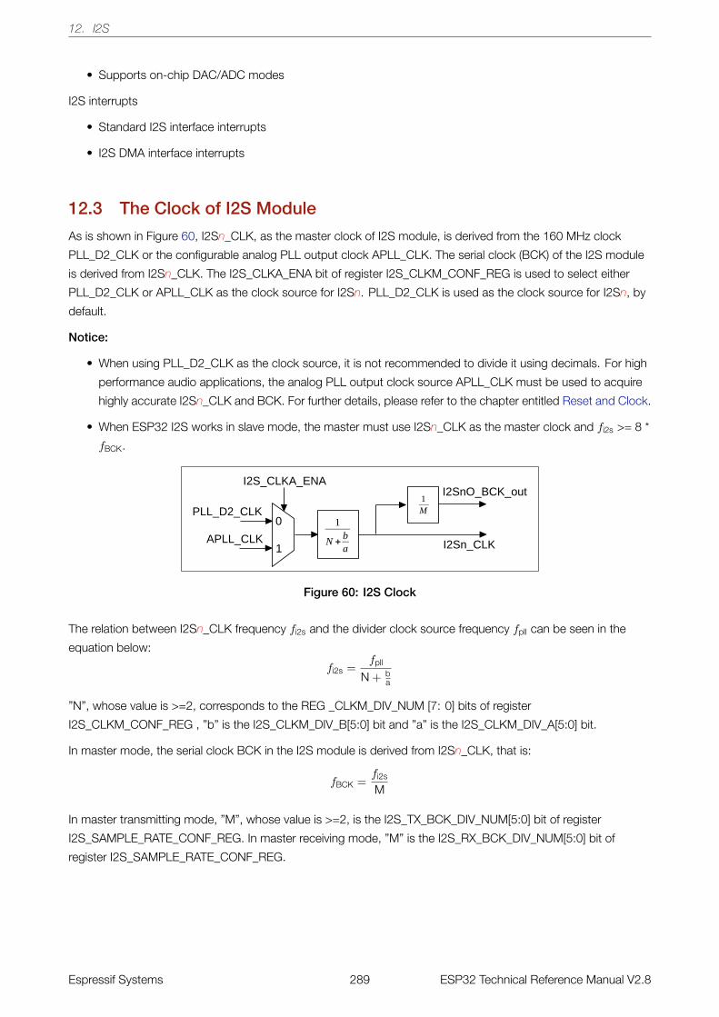
12. I2S
• Supports on-chip DAC/ADC modes
I2S interrupts
• Standard I2S interface interrupts
• I2S DMA interface interrupts
12.3 The Clock of I2S Module
As is shown in Figure 60, I2Sn_CLK, as the master clock of I2S module, is derived from the 160 MHz clock
PLL_D2_CLK or the configurable analog PLL output clock APLL_CLK. The serial clock (BCK) of the I2S module
is derived from I2Sn_CLK. The I2S_CLKA_ENA bit of register I2S_CLKM_CONF_REG is used to select either
PLL_D2_CLK or APLL_CLK as the clock source for I2Sn. PLL_D2_CLK is used as the clock source for I2Sn, by
default.
Notice:
• When using PLL_D2_CLK as the clock source, it is not recommended to divide it using decimals. For high
performance audio applications, the analog PLL output clock source APLL_CLK must be used to acquire
highly accurate I2Sn_CLK and BCK. For further details, please refer to the chapter entitled Reset and Clock.
• When ESP32 I2S works in slave mode, the master must use I2Sn_CLK as the master clock and fi2s >= 8 *
fBCK.
Figure 60: I2S Clock
The relation between I2Sn_CLK frequency fi2s and the divider clock source frequency fpll can be seen in the
equation below:
fi2s =fpll
N + ba
”N”, whose value is >=2, corresponds to the REG _CLKM_DIV_NUM [7: 0] bits of register
I2S_CLKM_CONF_REG , ”b” is the I2S_CLKM_DIV_B[5:0] bit and ”a” is the I2S_CLKM_DIV_A[5:0] bit.
In master mode, the serial clock BCK in the I2S module is derived from I2Sn_CLK, that is:
fBCK =fi2s
M
In master transmitting mode, ”M”, whose value is >=2, is the I2S_TX_BCK_DIV_NUM[5:0] bit of register
I2S_SAMPLE_RATE_CONF_REG. In master receiving mode, ”M” is the I2S_RX_BCK_DIV_NUM[5:0] bit of
register I2S_SAMPLE_RATE_CONF_REG.
Espressif Systems 289 ESP32 Technical Reference Manual V2.8
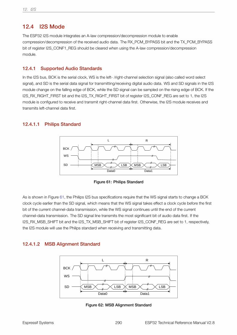
12. I2S
12.4 I2S Mode
The ESP32 I2S module integrates an A-law compression/decompression module to enable
compression/decompression of the received audio data. The RX_PCM_BYPASS bit and the TX_PCM_BYPASS
bit of register I2S_CONF1_REG should be cleared when using the A-law compression/decompression
module.
12.4.1 Supported Audio Standards
In the I2S bus, BCK is the serial clock, WS is the left- /right-channel selection signal (also called word select
signal), and SD is the serial data signal for transmitting/receiving digital audio data. WS and SD signals in the I2S
module change on the falling edge of BCK, while the SD signal can be sampled on the rising edge of BCK. If the
I2S_RX_RIGHT_FIRST bit and the I2S_TX_RIGHT_FIRST bit of register I2S_CONF_REG are set to 1, the I2S
module is configured to receive and transmit right-channel data first. Otherwise, the I2S module receives and
transmits left-channel data first.
12.4.1.1 Philips Standard
Figure 61: Philips Standard
As is shown in Figure 61, the Philips I2S bus specifications require that the WS signal starts to change a BCK
clock cycle earlier than the SD signal, which means that the WS signal takes effect a clock cycle before the first
bit of the current channel-data transmission, while the WS signal continues until the end of the current
channel-data transmission. The SD signal line transmits the most significant bit of audio data first. If the
I2S_RX_MSB_SHIFT bit and the I2S_TX_MSB_SHIFT bit of register I2S_CONF_REG are set to 1, respectively,
the I2S module will use the Philips standard when receiving and transmitting data.
12.4.1.2 MSB Alignment Standard
Figure 62: MSB Alignment Standard
Espressif Systems 290 ESP32 Technical Reference Manual V2.8
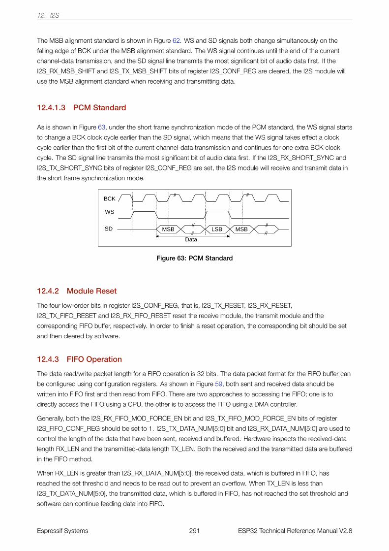
12. I2S
The MSB alignment standard is shown in Figure 62. WS and SD signals both change simultaneously on the
falling edge of BCK under the MSB alignment standard. The WS signal continues until the end of the current
channel-data transmission, and the SD signal line transmits the most significant bit of audio data first. If the
I2S_RX_MSB_SHIFT and I2S_TX_MSB_SHIFT bits of register I2S_CONF_REG are cleared, the I2S module will
use the MSB alignment standard when receiving and transmitting data.
12.4.1.3 PCM Standard
As is shown in Figure 63, under the short frame synchronization mode of the PCM standard, the WS signal starts
to change a BCK clock cycle earlier than the SD signal, which means that the WS signal takes effect a clock
cycle earlier than the first bit of the current channel-data transmission and continues for one extra BCK clock
cycle. The SD signal line transmits the most significant bit of audio data first. If the I2S_RX_SHORT_SYNC and
I2S_TX_SHORT_SYNC bits of register I2S_CONF_REG are set, the I2S module will receive and transmit data in
the short frame synchronization mode.
Figure 63: PCM Standard
12.4.2 Module Reset
The four low-order bits in register I2S_CONF_REG, that is, I2S_TX_RESET, I2S_RX_RESET,
I2S_TX_FIFO_RESET and I2S_RX_FIFO_RESET reset the receive module, the transmit module and the
corresponding FIFO buffer, respectively. In order to finish a reset operation, the corresponding bit should be set
and then cleared by software.
12.4.3 FIFO Operation
The data read/write packet length for a FIFO operation is 32 bits. The data packet format for the FIFO buffer can
be configured using configuration registers. As shown in Figure 59, both sent and received data should be
written into FIFO first and then read from FIFO. There are two approaches to accessing the FIFO; one is to
directly access the FIFO using a CPU, the other is to access the FIFO using a DMA controller.
Generally, both the I2S_RX_FIFO_MOD_FORCE_EN bit and I2S_TX_FIFO_MOD_FORCE_EN bits of register
I2S_FIFO_CONF_REG should be set to 1. I2S_TX_DATA_NUM[5:0] bit and I2S_RX_DATA_NUM[5:0] are used to
control the length of the data that have been sent, received and buffered. Hardware inspects the received-data
length RX_LEN and the transmitted-data length TX_LEN. Both the received and the transmitted data are buffered
in the FIFO method.
When RX_LEN is greater than I2S_RX_DATA_NUM[5:0], the received data, which is buffered in FIFO, has
reached the set threshold and needs to be read out to prevent an overflow. When TX_LEN is less than
I2S_TX_DATA_NUM[5:0], the transmitted data, which is buffered in FIFO, has not reached the set threshold and
software can continue feeding data into FIFO.
Espressif Systems 291 ESP32 Technical Reference Manual V2.8
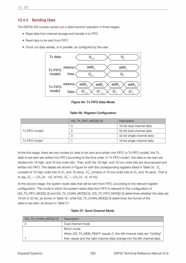
12. I2S
12.4.4 Sending Data
The ESP32 I2S module carries out a data-transmit operation in three stages:
• Read data from internal storage and transfer it to FIFO
• Read data to be sent from FIFO
• Clock out data serially, or in parallel, as configured by the user
Figure 64: Tx FIFO Data Mode
Table 56: Register Configuration
I2S_TX_FIFO_MOD[2:0] Description
Tx FIFO mode0
0 16-bit dual channel data
2 32-bit dual channel data
3 32-bit single channel data
Tx FIFO mode1 1 16-bit single channel data
At the first stage, there are two modes for data to be sent and written into FIFO. In Tx FIFO mode0, the Tx
data-to-be-sent are written into FIFO according to the time order. In Tx FIFO mode1, the data-to-be-sent are
divided into 16 high- and 16 low-order bits. Then, both the 16 high- and 16 low-order bits are recomposed and
written into FIFO. The details are shown in Figure 64 with the corresponding registers listed in Table 56. D′
n
consists of 16 high-order bits of Dn and 16 zeros. D′′
n consists of 16 low-order bits of Dn and 16 zeros. That is
to say, D′
n = {Dn[31 : 16], 16′h0}, D′′
n = {Dn[15 : 0], 16′h0}.
At the second stage, the system reads data that will be sent from FIFO, according to the relevant register
configuration. The mode in which the system reads data from FIFO is relevant to the configuration of
I2S_TX_FIFO_MOD[2.0] and I2S_TX_CHAN_MOD[2:0]. I2S_TX_FIFO_MOD[2.0] determines whether the data are
16-bit or 32-bit, as shown in Table 56, while I2S_TX_CHAN_MOD[2:0] determines the format of the
data-to-be-sent, as shown in Table 57.
Table 57: Send Channel Mode
I2S_TX_CHAN_MOD[2:0] Description
0 Dual channel mode
1
Mono mode
When I2S_TX_MSB_RIGHT equals 0, the left-channel data are ”holding”
their values and the right-channel data change into the left-channel data.
Espressif Systems 292 ESP32 Technical Reference Manual V2.8
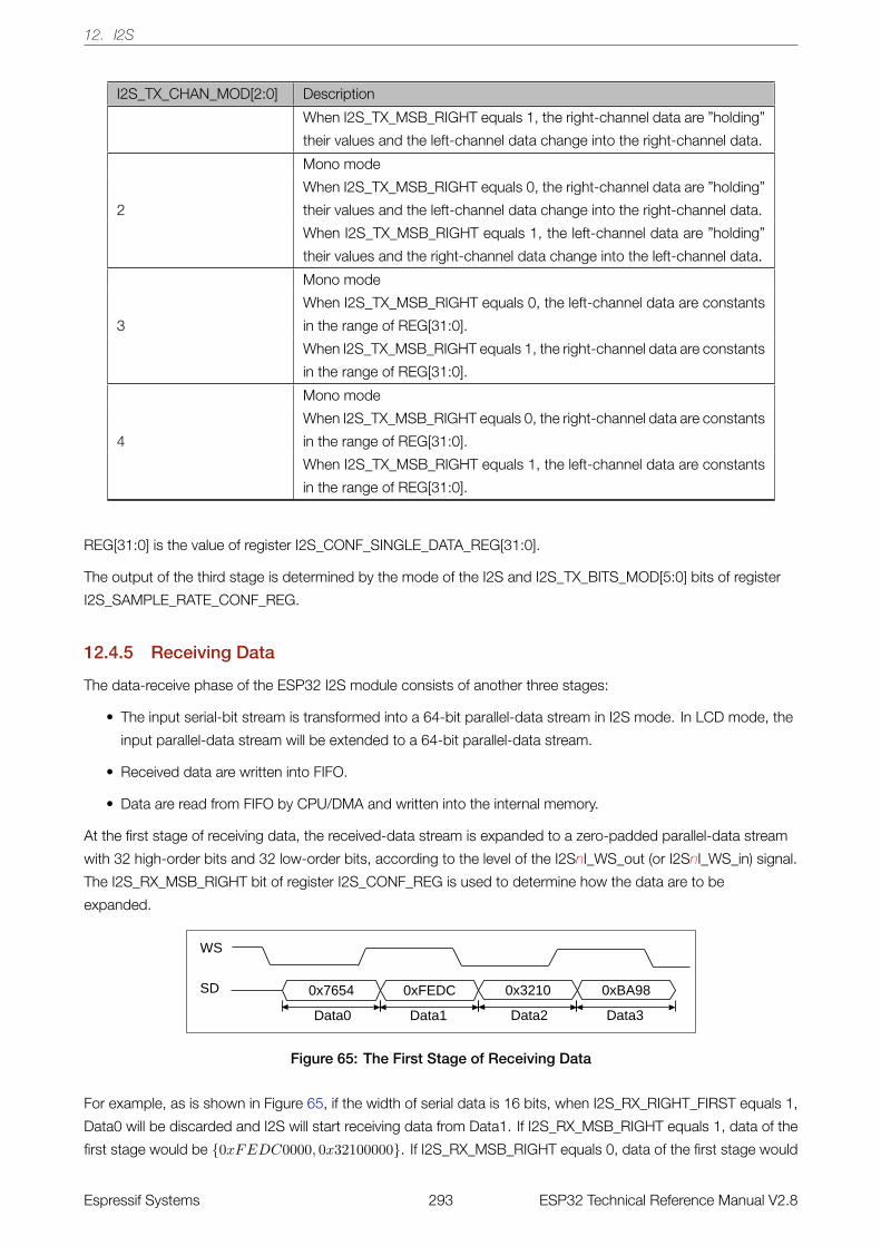
12. I2S
I2S_TX_CHAN_MOD[2:0] Description
When I2S_TX_MSB_RIGHT equals 1, the right-channel data are ”holding”
their values and the left-channel data change into the right-channel data.
2
Mono mode
When I2S_TX_MSB_RIGHT equals 0, the right-channel data are ”holding”
their values and the left-channel data change into the right-channel data.
When I2S_TX_MSB_RIGHT equals 1, the left-channel data are ”holding”
their values and the right-channel data change into the left-channel data.
3
Mono mode
When I2S_TX_MSB_RIGHT equals 0, the left-channel data are constants
in the range of REG[31:0].
When I2S_TX_MSB_RIGHT equals 1, the right-channel data are constants
in the range of REG[31:0].
4
Mono mode
When I2S_TX_MSB_RIGHT equals 0, the right-channel data are constants
in the range of REG[31:0].
When I2S_TX_MSB_RIGHT equals 1, the left-channel data are constants
in the range of REG[31:0].
REG[31:0] is the value of register I2S_CONF_SINGLE_DATA_REG[31:0].
The output of the third stage is determined by the mode of the I2S and I2S_TX_BITS_MOD[5:0] bits of register
I2S_SAMPLE_RATE_CONF_REG.
12.4.5 Receiving Data
The data-receive phase of the ESP32 I2S module consists of another three stages:
• The input serial-bit stream is transformed into a 64-bit parallel-data stream in I2S mode. In LCD mode, the
input parallel-data stream will be extended to a 64-bit parallel-data stream.
• Received data are written into FIFO.
• Data are read from FIFO by CPU/DMA and written into the internal memory.
At the first stage of receiving data, the received-data stream is expanded to a zero-padded parallel-data stream
with 32 high-order bits and 32 low-order bits, according to the level of the I2SnI_WS_out (or I2SnI_WS_in) signal.
The I2S_RX_MSB_RIGHT bit of register I2S_CONF_REG is used to determine how the data are to be
expanded.
Figure 65: The First Stage of Receiving Data
For example, as is shown in Figure 65, if the width of serial data is 16 bits, when I2S_RX_RIGHT_FIRST equals 1,
Data0 will be discarded and I2S will start receiving data from Data1. If I2S_RX_MSB_RIGHT equals 1, data of the
first stage would be {0xFEDC0000, 0x32100000}. If I2S_RX_MSB_RIGHT equals 0, data of the first stage would
Espressif Systems 293 ESP32 Technical Reference Manual V2.8
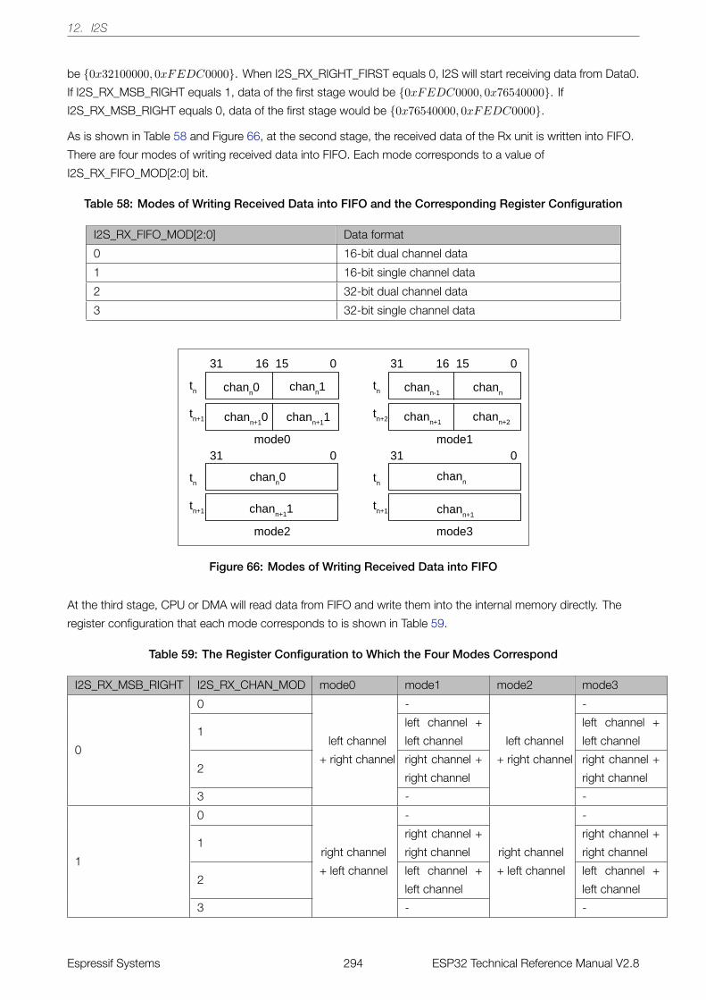
12. I2S
be {0x32100000, 0xFEDC0000}. When I2S_RX_RIGHT_FIRST equals 0, I2S will start receiving data from Data0.
If I2S_RX_MSB_RIGHT equals 1, data of the first stage would be {0xFEDC0000, 0x76540000}. If
I2S_RX_MSB_RIGHT equals 0, data of the first stage would be {0x76540000, 0xFEDC0000}.
As is shown in Table 58 and Figure 66, at the second stage, the received data of the Rx unit is written into FIFO.
There are four modes of writing received data into FIFO. Each mode corresponds to a value of
I2S_RX_FIFO_MOD[2:0] bit.
Table 58: Modes of Writing Received Data into FIFO and the Corresponding Register Configuration
I2S_RX_FIFO_MOD[2:0] Data format
0 16-bit dual channel data
1 16-bit single channel data
2 32-bit dual channel data
3 32-bit single channel data
Figure 66: Modes of Writing Received Data into FIFO
At the third stage, CPU or DMA will read data from FIFO and write them into the internal memory directly. The
register configuration that each mode corresponds to is shown in Table 59.
Table 59: The Register Configuration to Which the Four Modes Correspond
I2S_RX_MSB_RIGHT I2S_RX_CHAN_MOD mode0 mode1 mode2 mode3
0
0
left channel
+ right channel
-
left channel
+ right channel
-
1left channel +
left channel
left channel +
left channel
2right channel +
right channel
right channel +
right channel
3 - -
1
0
right channel
+ left channel
-
right channel
+ left channel
-
1right channel +
right channel
right channel +
right channel
2left channel +
left channel
left channel +
left channel
3 - -
Espressif Systems 294 ESP32 Technical Reference Manual V2.8
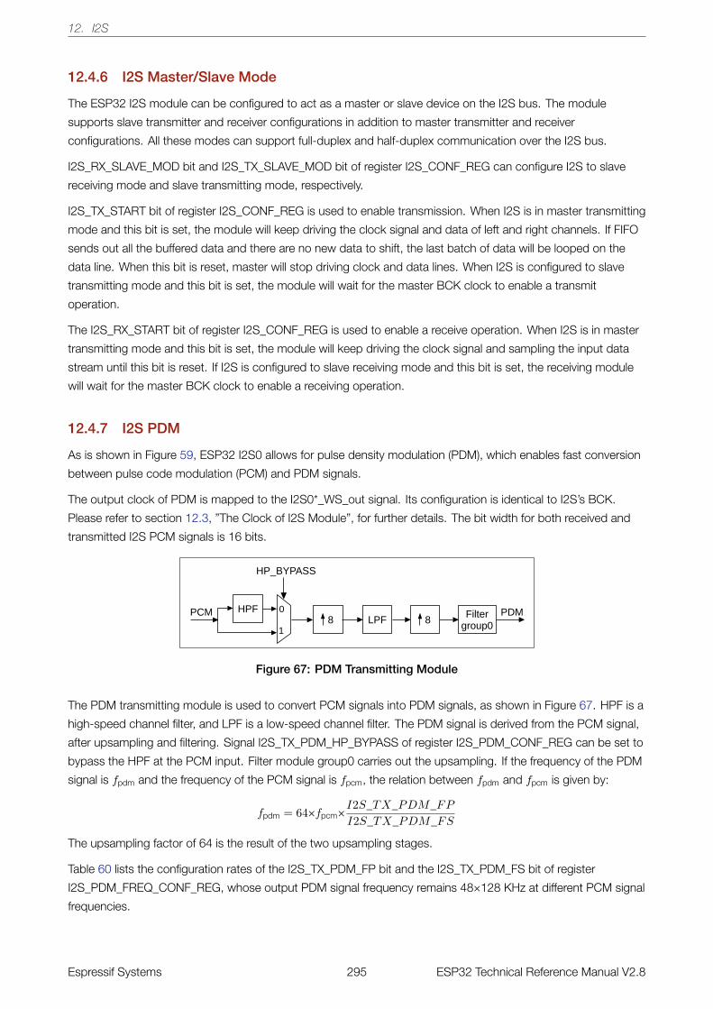
12. I2S
12.4.6 I2S Master/Slave Mode
The ESP32 I2S module can be configured to act as a master or slave device on the I2S bus. The module
supports slave transmitter and receiver configurations in addition to master transmitter and receiver
configurations. All these modes can support full-duplex and half-duplex communication over the I2S bus.
I2S_RX_SLAVE_MOD bit and I2S_TX_SLAVE_MOD bit of register I2S_CONF_REG can configure I2S to slave
receiving mode and slave transmitting mode, respectively.
I2S_TX_START bit of register I2S_CONF_REG is used to enable transmission. When I2S is in master transmitting
mode and this bit is set, the module will keep driving the clock signal and data of left and right channels. If FIFO
sends out all the buffered data and there are no new data to shift, the last batch of data will be looped on the
data line. When this bit is reset, master will stop driving clock and data lines. When I2S is configured to slave
transmitting mode and this bit is set, the module will wait for the master BCK clock to enable a transmit
operation.
The I2S_RX_START bit of register I2S_CONF_REG is used to enable a receive operation. When I2S is in master
transmitting mode and this bit is set, the module will keep driving the clock signal and sampling the input data
stream until this bit is reset. If I2S is configured to slave receiving mode and this bit is set, the receiving module
will wait for the master BCK clock to enable a receiving operation.
12.4.7 I2S PDM
As is shown in Figure 59, ESP32 I2S0 allows for pulse density modulation (PDM), which enables fast conversion
between pulse code modulation (PCM) and PDM signals.
The output clock of PDM is mapped to the I2S0*_WS_out signal. Its configuration is identical to I2S’s BCK.
Please refer to section 12.3, ”The Clock of I2S Module”, for further details. The bit width for both received and
transmitted I2S PCM signals is 16 bits.
Figure 67: PDM Transmitting Module
The PDM transmitting module is used to convert PCM signals into PDM signals, as shown in Figure 67. HPF is a
high-speed channel filter, and LPF is a low-speed channel filter. The PDM signal is derived from the PCM signal,
after upsampling and filtering. Signal I2S_TX_PDM_HP_BYPASS of register I2S_PDM_CONF_REG can be set to
bypass the HPF at the PCM input. Filter module group0 carries out the upsampling. If the frequency of the PDM
signal is fpdm and the frequency of the PCM signal is fpcm, the relation between fpdm and fpcm is given by:
fpdm = 64×fpcm×I2S_TX_PDM_FP
I2S_TX_PDM_FS
The upsampling factor of 64 is the result of the two upsampling stages.
Table 60 lists the configuration rates of the I2S_TX_PDM_FP bit and the I2S_TX_PDM_FS bit of register
I2S_PDM_FREQ_CONF_REG, whose output PDM signal frequency remains 48×128 KHz at different PCM signal
frequencies.
Espressif Systems 295 ESP32 Technical Reference Manual V2.8
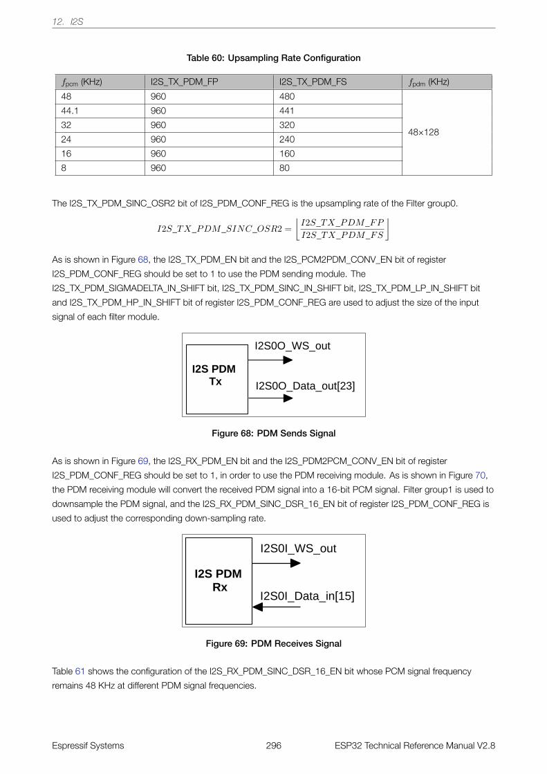
12. I2S
Table 60: Upsampling Rate Configuration
fpcm (KHz) I2S_TX_PDM_FP I2S_TX_PDM_FS fpdm (KHz)
48 960 480
48×128
44.1 960 441
32 960 320
24 960 240
16 960 160
8 960 80
The I2S_TX_PDM_SINC_OSR2 bit of I2S_PDM_CONF_REG is the upsampling rate of the Filter group0.
I2S_TX_PDM_SINC_OSR2 =
⌊I2S_TX_PDM_FP
I2S_TX_PDM_FS
⌋
As is shown in Figure 68, the I2S_TX_PDM_EN bit and the I2S_PCM2PDM_CONV_EN bit of register
I2S_PDM_CONF_REG should be set to 1 to use the PDM sending module. The
I2S_TX_PDM_SIGMADELTA_IN_SHIFT bit, I2S_TX_PDM_SINC_IN_SHIFT bit, I2S_TX_PDM_LP_IN_SHIFT bit
and I2S_TX_PDM_HP_IN_SHIFT bit of register I2S_PDM_CONF_REG are used to adjust the size of the input
signal of each filter module.
Figure 68: PDM Sends Signal
As is shown in Figure 69, the I2S_RX_PDM_EN bit and the I2S_PDM2PCM_CONV_EN bit of register
I2S_PDM_CONF_REG should be set to 1, in order to use the PDM receiving module. As is shown in Figure 70,
the PDM receiving module will convert the received PDM signal into a 16-bit PCM signal. Filter group1 is used to
downsample the PDM signal, and the I2S_RX_PDM_SINC_DSR_16_EN bit of register I2S_PDM_CONF_REG is
used to adjust the corresponding down-sampling rate.
Figure 69: PDM Receives Signal
Table 61 shows the configuration of the I2S_RX_PDM_SINC_DSR_16_EN bit whose PCM signal frequency
remains 48 KHz at different PDM signal frequencies.
Espressif Systems 296 ESP32 Technical Reference Manual V2.8
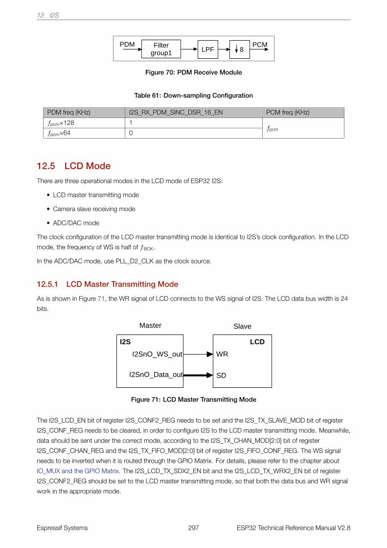
12. I2S
Figure 70: PDM Receive Module
Table 61: Down-sampling Configuration
PDM freq (KHz) I2S_RX_PDM_SINC_DSR_16_EN PCM freq (KHz)
fpcm×128 1fpcm
fpcm×64 0
12.5 LCD Mode
There are three operational modes in the LCD mode of ESP32 I2S:
• LCD master transmitting mode
• Camera slave receiving mode
• ADC/DAC mode
The clock configuration of the LCD master transmitting mode is identical to I2S’s clock configuration. In the LCD
mode, the frequency of WS is half of fBCK.
In the ADC/DAC mode, use PLL_D2_CLK as the clock source.
12.5.1 LCD Master Transmitting Mode
As is shown in Figure 71, the WR signal of LCD connects to the WS signal of I2S. The LCD data bus width is 24
bits.
Figure 71: LCD Master Transmitting Mode
The I2S_LCD_EN bit of register I2S_CONF2_REG needs to be set and the I2S_TX_SLAVE_MOD bit of register
I2S_CONF_REG needs to be cleared, in order to configure I2S to the LCD master transmitting mode. Meanwhile,
data should be sent under the correct mode, according to the I2S_TX_CHAN_MOD[2:0] bit of register
I2S_CONF_CHAN_REG and the I2S_TX_FIFO_MOD[2:0] bit of register I2S_FIFO_CONF_REG. The WS signal
needs to be inverted when it is routed through the GPIO Matrix. For details, please refer to the chapter about
IO_MUX and the GPIO Matrix. The I2S_LCD_TX_SDX2_EN bit and the I2S_LCD_TX_WRX2_EN bit of register
I2S_CONF2_REG should be set to the LCD master transmitting mode, so that both the data bus and WR signal
work in the appropriate mode.
Espressif Systems 297 ESP32 Technical Reference Manual V2.8
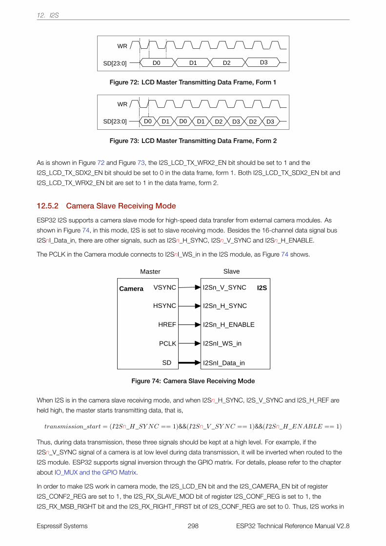
12. I2S
Figure 72: LCD Master Transmitting Data Frame, Form 1
Figure 73: LCD Master Transmitting Data Frame, Form 2
As is shown in Figure 72 and Figure 73, the I2S_LCD_TX_WRX2_EN bit should be set to 1 and the
I2S_LCD_TX_SDX2_EN bit should be set to 0 in the data frame, form 1. Both I2S_LCD_TX_SDX2_EN bit and
I2S_LCD_TX_WRX2_EN bit are set to 1 in the data frame, form 2.
12.5.2 Camera Slave Receiving Mode
ESP32 I2S supports a camera slave mode for high-speed data transfer from external camera modules. As
shown in Figure 74, in this mode, I2S is set to slave receiving mode. Besides the 16-channel data signal bus
I2SnI_Data_in, there are other signals, such as I2Sn_H_SYNC, I2Sn_V_SYNC and I2Sn_H_ENABLE.
The PCLK in the Camera module connects to I2SnI_WS_in in the I2S module, as Figure 74 shows.
Figure 74: Camera Slave Receiving Mode
When I2S is in the camera slave receiving mode, and when I2Sn_H_SYNC, I2S_V_SYNC and I2S_H_REF are
held high, the master starts transmitting data, that is,
transmission_start = (I2Sn_H_SY NC == 1)&&(I2Sn_V _SY NC == 1)&&(I2Sn_H_ENABLE == 1)
Thus, during data transmission, these three signals should be kept at a high level. For example, if the
I2Sn_V_SYNC signal of a camera is at low level during data transmission, it will be inverted when routed to the
I2S module. ESP32 supports signal inversion through the GPIO matrix. For details, please refer to the chapter
about IO_MUX and the GPIO Matrix.
In order to make I2S work in camera mode, the I2S_LCD_EN bit and the I2S_CAMERA_EN bit of register
I2S_CONF2_REG are set to 1, the I2S_RX_SLAVE_MOD bit of register I2S_CONF_REG is set to 1, the
I2S_RX_MSB_RIGHT bit and the I2S_RX_RIGHT_FIRST bit of I2S_CONF_REG are set to 0. Thus, I2S works in
Espressif Systems 298 ESP32 Technical Reference Manual V2.8
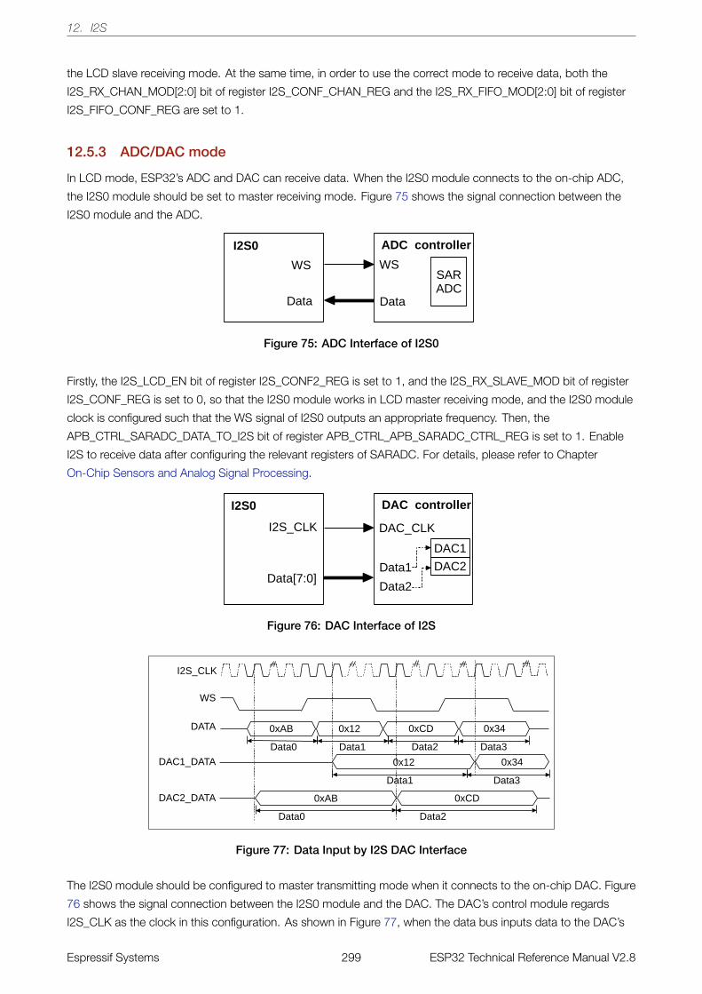
12. I2S
the LCD slave receiving mode. At the same time, in order to use the correct mode to receive data, both the
I2S_RX_CHAN_MOD[2:0] bit of register I2S_CONF_CHAN_REG and the I2S_RX_FIFO_MOD[2:0] bit of register
I2S_FIFO_CONF_REG are set to 1.
12.5.3 ADC/DAC mode
In LCD mode, ESP32’s ADC and DAC can receive data. When the I2S0 module connects to the on-chip ADC,
the I2S0 module should be set to master receiving mode. Figure 75 shows the signal connection between the
I2S0 module and the ADC.
Figure 75: ADC Interface of I2S0
Firstly, the I2S_LCD_EN bit of register I2S_CONF2_REG is set to 1, and the I2S_RX_SLAVE_MOD bit of register
I2S_CONF_REG is set to 0, so that the I2S0 module works in LCD master receiving mode, and the I2S0 module
clock is configured such that the WS signal of I2S0 outputs an appropriate frequency. Then, the
APB_CTRL_SARADC_DATA_TO_I2S bit of register APB_CTRL_APB_SARADC_CTRL_REG is set to 1. Enable
I2S to receive data after configuring the relevant registers of SARADC. For details, please refer to Chapter
On-Chip Sensors and Analog Signal Processing.
Figure 76: DAC Interface of I2S
Figure 77: Data Input by I2S DAC Interface
The I2S0 module should be configured to master transmitting mode when it connects to the on-chip DAC. Figure
76 shows the signal connection between the I2S0 module and the DAC. The DAC’s control module regards
I2S_CLK as the clock in this configuration. As shown in Figure 77, when the data bus inputs data to the DAC’s
Espressif Systems 299 ESP32 Technical Reference Manual V2.8
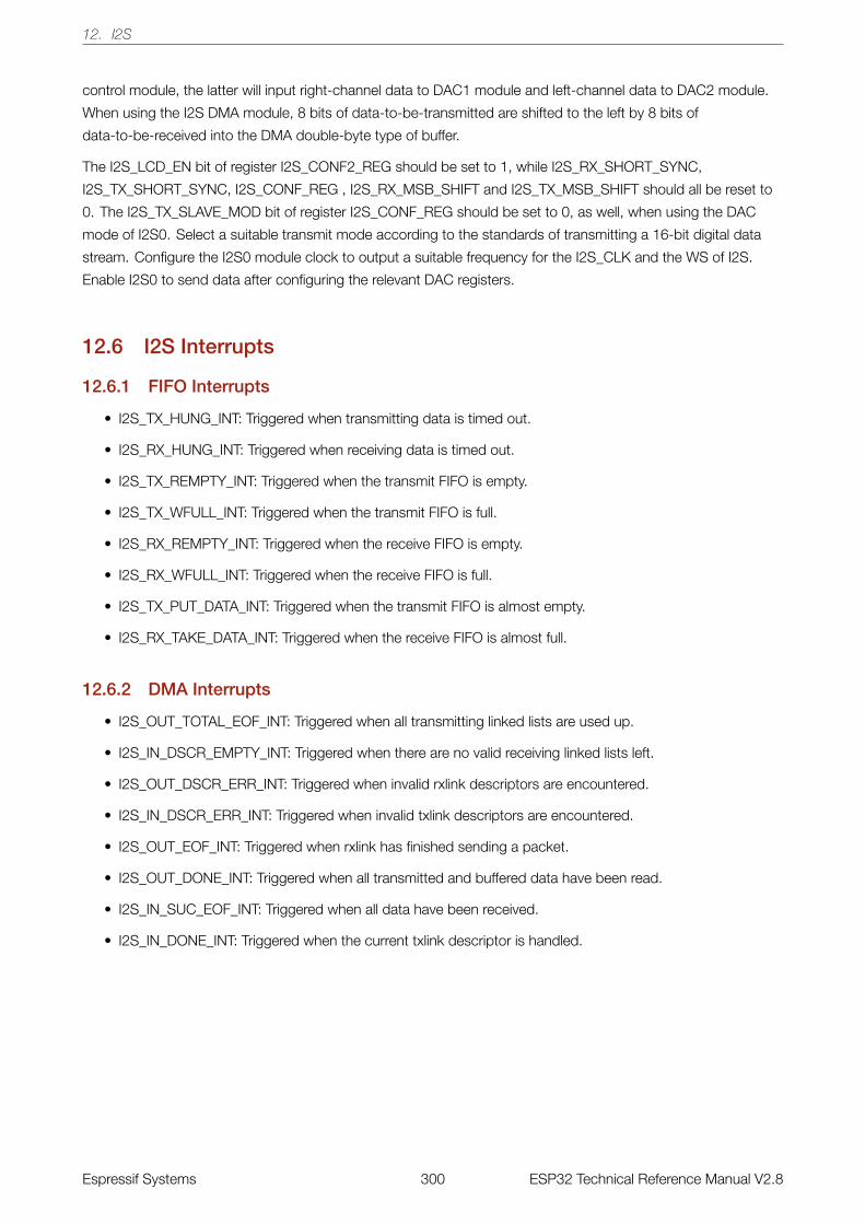
12. I2S
control module, the latter will input right-channel data to DAC1 module and left-channel data to DAC2 module.
When using the I2S DMA module, 8 bits of data-to-be-transmitted are shifted to the left by 8 bits of
data-to-be-received into the DMA double-byte type of buffer.
The I2S_LCD_EN bit of register I2S_CONF2_REG should be set to 1, while I2S_RX_SHORT_SYNC,
I2S_TX_SHORT_SYNC, I2S_CONF_REG , I2S_RX_MSB_SHIFT and I2S_TX_MSB_SHIFT should all be reset to
0. The I2S_TX_SLAVE_MOD bit of register I2S_CONF_REG should be set to 0, as well, when using the DAC
mode of I2S0. Select a suitable transmit mode according to the standards of transmitting a 16-bit digital data
stream. Configure the I2S0 module clock to output a suitable frequency for the I2S_CLK and the WS of I2S.
Enable I2S0 to send data after configuring the relevant DAC registers.
12.6 I2S Interrupts
12.6.1 FIFO Interrupts
• I2S_TX_HUNG_INT: Triggered when transmitting data is timed out.
• I2S_RX_HUNG_INT: Triggered when receiving data is timed out.
• I2S_TX_REMPTY_INT: Triggered when the transmit FIFO is empty.
• I2S_TX_WFULL_INT: Triggered when the transmit FIFO is full.
• I2S_RX_REMPTY_INT: Triggered when the receive FIFO is empty.
• I2S_RX_WFULL_INT: Triggered when the receive FIFO is full.
• I2S_TX_PUT_DATA_INT: Triggered when the transmit FIFO is almost empty.
• I2S_RX_TAKE_DATA_INT: Triggered when the receive FIFO is almost full.
12.6.2 DMA Interrupts
• I2S_OUT_TOTAL_EOF_INT: Triggered when all transmitting linked lists are used up.
• I2S_IN_DSCR_EMPTY_INT: Triggered when there are no valid receiving linked lists left.
• I2S_OUT_DSCR_ERR_INT: Triggered when invalid rxlink descriptors are encountered.
• I2S_IN_DSCR_ERR_INT: Triggered when invalid txlink descriptors are encountered.
• I2S_OUT_EOF_INT: Triggered when rxlink has finished sending a packet.
• I2S_OUT_DONE_INT: Triggered when all transmitted and buffered data have been read.
• I2S_IN_SUC_EOF_INT: Triggered when all data have been received.
• I2S_IN_DONE_INT: Triggered when the current txlink descriptor is handled.
Espressif Systems 300 ESP32 Technical Reference Manual V2.8
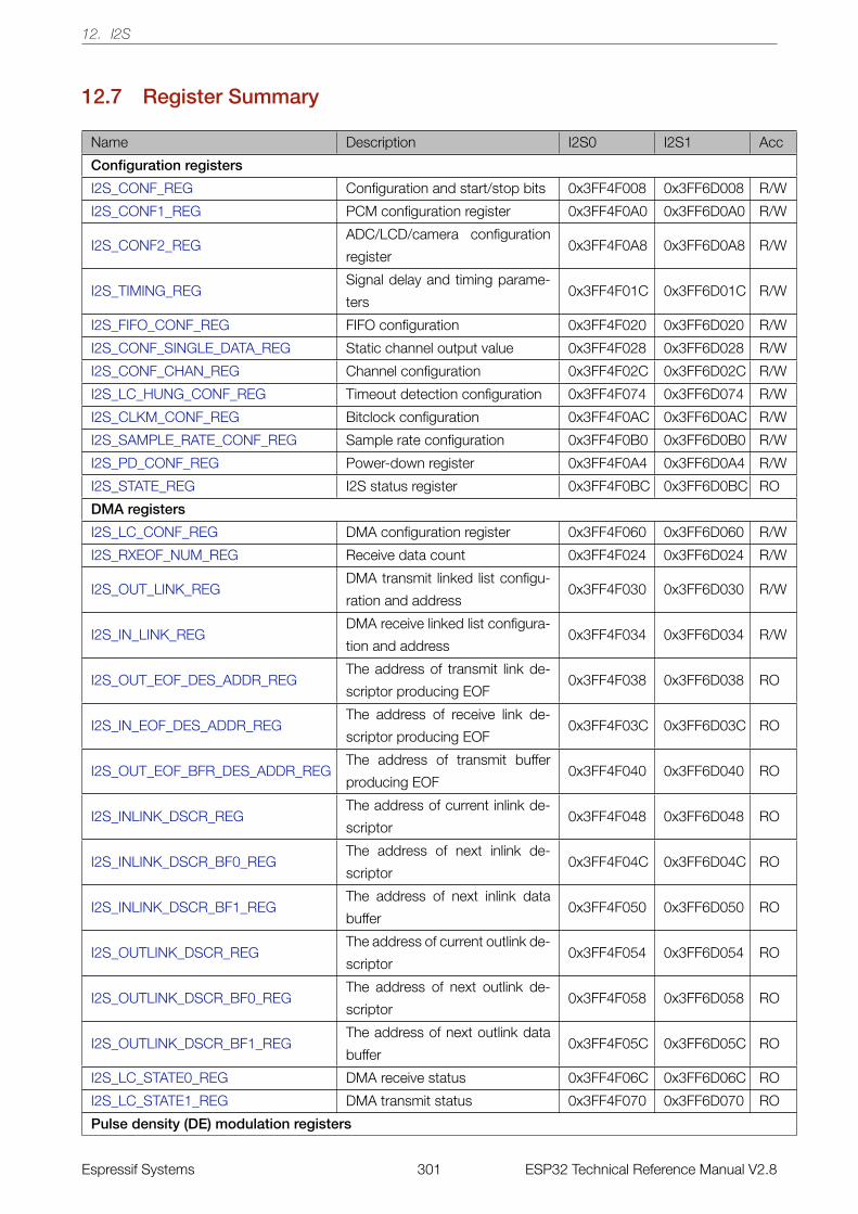
12. I2S
12.7 Register Summary
Name Description I2S0 I2S1 Acc
Configuration registers
I2S_CONF_REG Configuration and start/stop bits 0x3FF4F008 0x3FF6D008 R/W
I2S_CONF1_REG PCM configuration register 0x3FF4F0A0 0x3FF6D0A0 R/W
I2S_CONF2_REGADC/LCD/camera configuration
register0x3FF4F0A8 0x3FF6D0A8 R/W
I2S_TIMING_REGSignal delay and timing parame-
ters0x3FF4F01C 0x3FF6D01C R/W
I2S_FIFO_CONF_REG FIFO configuration 0x3FF4F020 0x3FF6D020 R/W
I2S_CONF_SINGLE_DATA_REG Static channel output value 0x3FF4F028 0x3FF6D028 R/W
I2S_CONF_CHAN_REG Channel configuration 0x3FF4F02C 0x3FF6D02C R/W
I2S_LC_HUNG_CONF_REG Timeout detection configuration 0x3FF4F074 0x3FF6D074 R/W
I2S_CLKM_CONF_REG Bitclock configuration 0x3FF4F0AC 0x3FF6D0AC R/W
I2S_SAMPLE_RATE_CONF_REG Sample rate configuration 0x3FF4F0B0 0x3FF6D0B0 R/W
I2S_PD_CONF_REG Power-down register 0x3FF4F0A4 0x3FF6D0A4 R/W
I2S_STATE_REG I2S status register 0x3FF4F0BC 0x3FF6D0BC RO
DMA registers
I2S_LC_CONF_REG DMA configuration register 0x3FF4F060 0x3FF6D060 R/W
I2S_RXEOF_NUM_REG Receive data count 0x3FF4F024 0x3FF6D024 R/W
I2S_OUT_LINK_REGDMA transmit linked list configu-
ration and address0x3FF4F030 0x3FF6D030 R/W
I2S_IN_LINK_REGDMA receive linked list configura-
tion and address0x3FF4F034 0x3FF6D034 R/W
I2S_OUT_EOF_DES_ADDR_REGThe address of transmit link de-
scriptor producing EOF0x3FF4F038 0x3FF6D038 RO
I2S_IN_EOF_DES_ADDR_REGThe address of receive link de-
scriptor producing EOF0x3FF4F03C 0x3FF6D03C RO
I2S_OUT_EOF_BFR_DES_ADDR_REGThe address of transmit buffer
producing EOF0x3FF4F040 0x3FF6D040 RO
I2S_INLINK_DSCR_REGThe address of current inlink de-
scriptor0x3FF4F048 0x3FF6D048 RO
I2S_INLINK_DSCR_BF0_REGThe address of next inlink de-
scriptor0x3FF4F04C 0x3FF6D04C RO
I2S_INLINK_DSCR_BF1_REGThe address of next inlink data
buffer0x3FF4F050 0x3FF6D050 RO
I2S_OUTLINK_DSCR_REGThe address of current outlink de-
scriptor0x3FF4F054 0x3FF6D054 RO
I2S_OUTLINK_DSCR_BF0_REGThe address of next outlink de-
scriptor0x3FF4F058 0x3FF6D058 RO
I2S_OUTLINK_DSCR_BF1_REGThe address of next outlink data
buffer0x3FF4F05C 0x3FF6D05C RO
I2S_LC_STATE0_REG DMA receive status 0x3FF4F06C 0x3FF6D06C RO
I2S_LC_STATE1_REG DMA transmit status 0x3FF4F070 0x3FF6D070 RO
Pulse density (DE) modulation registers
Espressif Systems 301 ESP32 Technical Reference Manual V2.8
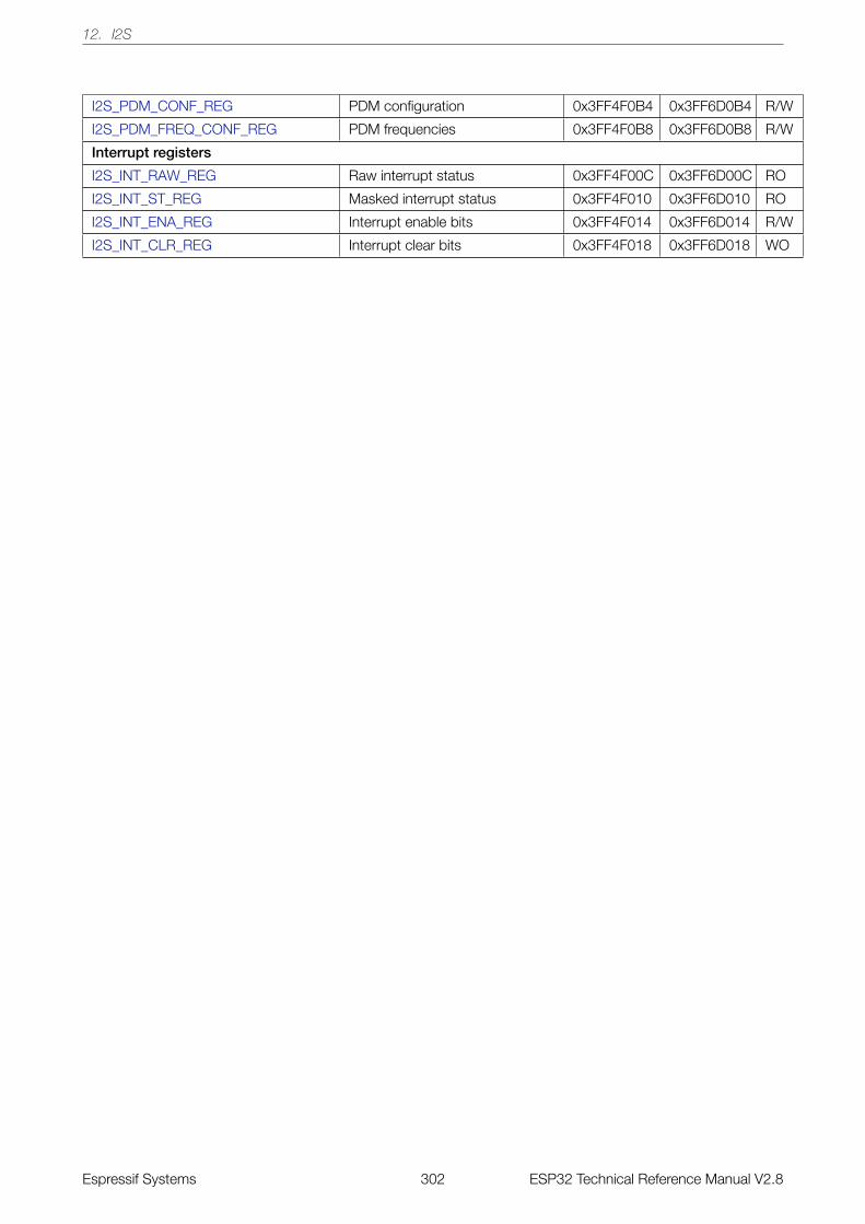
12. I2S
I2S_PDM_CONF_REG PDM configuration 0x3FF4F0B4 0x3FF6D0B4 R/W
I2S_PDM_FREQ_CONF_REG PDM frequencies 0x3FF4F0B8 0x3FF6D0B8 R/W
Interrupt registers
I2S_INT_RAW_REG Raw interrupt status 0x3FF4F00C 0x3FF6D00C RO
I2S_INT_ST_REG Masked interrupt status 0x3FF4F010 0x3FF6D010 RO
I2S_INT_ENA_REG Interrupt enable bits 0x3FF4F014 0x3FF6D014 R/W
I2S_INT_CLR_REG Interrupt clear bits 0x3FF4F018 0x3FF6D018 WO
Espressif Systems 302 ESP32 Technical Reference Manual V2.8

12. I2S
12.8 Registers
Register 12.1: I2S_CONF_REG (0x0008)
(rese
rved)
0 0 0 0 0 0 0 0 0 0 0 0 0
31 19
I2S_S
IG_L
OOPBACK
0
18
I2S_R
X_M
SB_RIG
HT
0
17
I2S_T
X_M
SB_RIG
HT
0
16
I2S_R
X_M
ONO
1
15
I2S_T
X_M
ONO
1
14
I2S_R
X_SHORT_
SYNC
1
13
I2S_T
X_SHORT_
SYNC
1
12
I2S_R
X_M
SB_SHIFT
0
11
I2S_T
X_M
SB_SHIFT
0
10
I2S_R
X_RIG
HT_FIR
ST
0
9
I2S_T
X_RIG
HT_FIR
ST
0
8
I2S_R
X_SLA
VE_MOD
0
7
I2S_T
X_SLA
VE_MOD
0
6
I2S_R
X_STA
RT
0
5
I2S_T
X_STA
RT
0
4
I2S_R
X_FIF
O_RESET
0
3
I2S_T
X_FIF
O_RESET
0
2
I2S_R
X_RESET
0
1
I2S_T
X_RESET
0
0
Reset
I2S_SIG_LOOPBACK Enable signal loopback mode, with transmitter module and receiver module
sharing the same WS and BCK signals. (R/W)
I2S_RX_MSB_RIGHT Set this to place right-channel data at the MSB in the receive FIFO. (R/W)
I2S_TX_MSB_RIGHT Set this bit to place right-channel data at the MSB in the transmit FIFO. (R/W)
I2S_RX_MONO Set this bit to enable receiver’s mono mode in PCM standard mode. (R/W)
I2S_TX_MONO Set this bit to enable transmitter’s mono mode in PCM standard mode. (R/W)
I2S_RX_SHORT_SYNC Set this bit to enable receiver in PCM standard mode. (R/W)
I2S_TX_SHORT_SYNC Set this bit to enable transmitter in PCM standard mode. (R/W)
I2S_RX_MSB_SHIFT Set this bit to enable receiver in Philips standard mode. (R/W)
I2S_TX_MSB_SHIFT Set this bit to enable transmitter in Philips standard mode. (R/W)
I2S_RX_RIGHT_FIRST Set this bit to receive right-channel data first. (R/W)
I2S_TX_RIGHT_FIRST Set this bit to transmit right-channel data first. (R/W)
I2S_RX_SLAVE_MOD Set this bit to enable slave receiver mode. (R/W)
I2S_TX_SLAVE_MOD Set this bit to enable slave transmitter mode. (R/W)
I2S_RX_START Set this bit to start receiving data. (R/W)
I2S_TX_START Set this bit to start transmitting data. (R/W)
I2S_RX_FIFO_RESET Set this bit to reset the receive FIFO. (R/W)
I2S_TX_FIFO_RESET Set this bit to reset the transmit FIFO. (R/W)
I2S_RX_RESET Set this bit to reset the receiver. (R/W)
I2S_TX_RESET Set this bit to reset the transmitter. (R/W)
Espressif Systems 303 ESP32 Technical Reference Manual V2.8
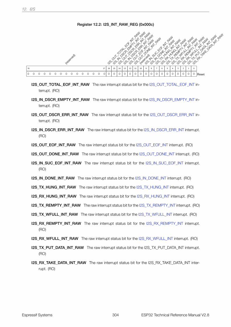
12. I2S
Register 12.2: I2S_INT_RAW_REG (0x000c)
(rese
rved)
0 0 0 0 0 0 0 0 0 0 0 0 0 0 0
31 17
I2S_O
UT_TO
TAL_
EOF_IN
T_RAW
0
16
I2S_IN
_DSCR_E
MPTY
_INT_
RAW
0
15
I2S_O
UT_DSCR_E
RR_INT_
RAW
0
14
I2S_IN
_DSCR_E
RR_INT_
RAW
0
13
I2S_O
UT_EOF_
INT_
RAW
0
12
I2S_O
UT_DONE_IN
T_RAW
0
11
(rese
rved)
0
10
I2S_IN
_SUC_E
OF_IN
T_RAW
0
9
I2S_IN
_DONE_IN
T_RAW
0
8
I2S_T
X_HUNG_IN
T_RAW
0
7
I2S_R
X_HUNG_IN
T_RAW
0
6
I2S_T
X_REM
PTY_IN
T_RAW
0
5
I2S_T
X_W
FULL
_INT_
RAW
0
4
I2S_R
X_REM
PTY_IN
T_RAW
0
3
I2S_R
X_W
FULL
_INT_
RAW
0
2
I2S_T
X_PUT_
DATA_IN
T_RAW
0
1
I2S_R
X_TA
KE_DAT
A_INT_
RAW
0
0
Reset
I2S_OUT_TOTAL_EOF_INT_RAW The raw interrupt status bit for the I2S_OUT_TOTAL_EOF_INT in-
terrupt. (RO)
I2S_IN_DSCR_EMPTY_INT_RAW The raw interrupt status bit for the I2S_IN_DSCR_EMPTY_INT in-
terrupt. (RO)
I2S_OUT_DSCR_ERR_INT_RAW The raw interrupt status bit for the I2S_OUT_DSCR_ERR_INT in-
terrupt. (RO)
I2S_IN_DSCR_ERR_INT_RAW The raw interrupt status bit for the I2S_IN_DSCR_ERR_INT interrupt.
(RO)
I2S_OUT_EOF_INT_RAW The raw interrupt status bit for the I2S_OUT_EOF_INT interrupt. (RO)
I2S_OUT_DONE_INT_RAW The raw interrupt status bit for the I2S_OUT_DONE_INT interrupt. (RO)
I2S_IN_SUC_EOF_INT_RAW The raw interrupt status bit for the I2S_IN_SUC_EOF_INT interrupt.
(RO)
I2S_IN_DONE_INT_RAW The raw interrupt status bit for the I2S_IN_DONE_INT interrupt. (RO)
I2S_TX_HUNG_INT_RAW The raw interrupt status bit for the I2S_TX_HUNG_INT interrupt. (RO)
I2S_RX_HUNG_INT_RAW The raw interrupt status bit for the I2S_RX_HUNG_INT interrupt. (RO)
I2S_TX_REMPTY_INT_RAW The raw interrupt status bit for the I2S_TX_REMPTY_INT interrupt. (RO)
I2S_TX_WFULL_INT_RAW The raw interrupt status bit for the I2S_TX_WFULL_INT interrupt. (RO)
I2S_RX_REMPTY_INT_RAW The raw interrupt status bit for the I2S_RX_REMPTY_INT interrupt.
(RO)
I2S_RX_WFULL_INT_RAW The raw interrupt status bit for the I2S_RX_WFULL_INT interrupt. (RO)
I2S_TX_PUT_DATA_INT_RAW The raw interrupt status bit for the I2S_TX_PUT_DATA_INT interrupt.
(RO)
I2S_RX_TAKE_DATA_INT_RAW The raw interrupt status bit for the I2S_RX_TAKE_DATA_INT inter-
rupt. (RO)
Espressif Systems 304 ESP32 Technical Reference Manual V2.8
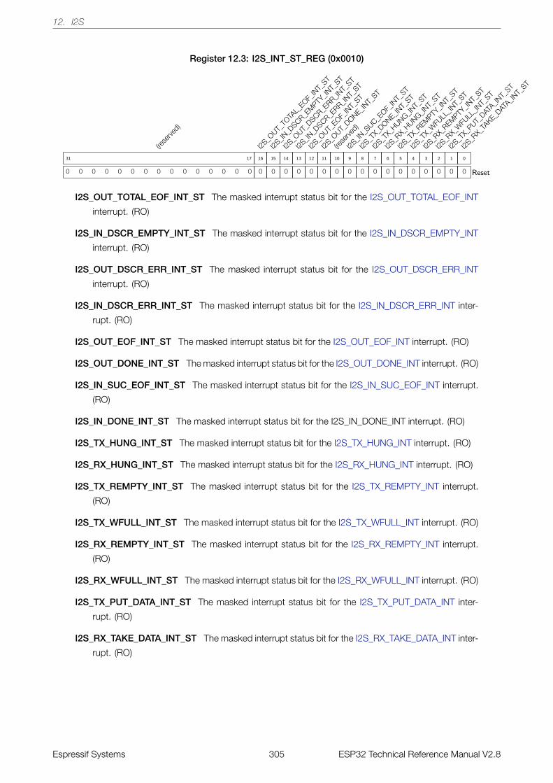
12. I2S
Register 12.3: I2S_INT_ST_REG (0x0010)
(rese
rved)
0 0 0 0 0 0 0 0 0 0 0 0 0 0 0
31 17
I2S_O
UT_TO
TAL_
EOF_IN
T_ST
0
16
I2S_IN
_DSCR_E
MPTY
_INT_
ST
0
15
I2S_O
UT_DSCR_E
RR_INT_
ST
0
14
I2S_IN
_DSCR_E
RR_INT_
ST
0
13
I2S_O
UT_EOF_
INT_
ST
0
12
I2S_O
UT_DONE_IN
T_ST
0
11
(rese
rved)
0
10
I2S_IN
_SUC_E
OF_IN
T_ST
0
9
I2S_T
X_DONE_IN
T_ST
0
8
I2S_T
X_HUNG_IN
T_ST
0
7
I2S_R
X_HUNG_IN
T_ST
0
6
I2S_T
X_REM
PTY_IN
T_ST
0
5
I2S_T
X_W
FULL
_INT_
ST
0
4
I2S_R
X_REM
PTY_IN
T_ST
0
3
I2S_R
X_W
FULL
_INT_
ST
0
2
I2S_T
X_PUT_
DATA_IN
T_ST
0
1
I2S_R
X_TA
KE_DAT
A_INT_
ST
0
0
Reset
I2S_OUT_TOTAL_EOF_INT_ST The masked interrupt status bit for the I2S_OUT_TOTAL_EOF_INT
interrupt. (RO)
I2S_IN_DSCR_EMPTY_INT_ST The masked interrupt status bit for the I2S_IN_DSCR_EMPTY_INT
interrupt. (RO)
I2S_OUT_DSCR_ERR_INT_ST The masked interrupt status bit for the I2S_OUT_DSCR_ERR_INT
interrupt. (RO)
I2S_IN_DSCR_ERR_INT_ST The masked interrupt status bit for the I2S_IN_DSCR_ERR_INT inter-
rupt. (RO)
I2S_OUT_EOF_INT_ST The masked interrupt status bit for the I2S_OUT_EOF_INT interrupt. (RO)
I2S_OUT_DONE_INT_ST The masked interrupt status bit for the I2S_OUT_DONE_INT interrupt. (RO)
I2S_IN_SUC_EOF_INT_ST The masked interrupt status bit for the I2S_IN_SUC_EOF_INT interrupt.
(RO)
I2S_IN_DONE_INT_ST The masked interrupt status bit for the I2S_IN_DONE_INT interrupt. (RO)
I2S_TX_HUNG_INT_ST The masked interrupt status bit for the I2S_TX_HUNG_INT interrupt. (RO)
I2S_RX_HUNG_INT_ST The masked interrupt status bit for the I2S_RX_HUNG_INT interrupt. (RO)
I2S_TX_REMPTY_INT_ST The masked interrupt status bit for the I2S_TX_REMPTY_INT interrupt.
(RO)
I2S_TX_WFULL_INT_ST The masked interrupt status bit for the I2S_TX_WFULL_INT interrupt. (RO)
I2S_RX_REMPTY_INT_ST The masked interrupt status bit for the I2S_RX_REMPTY_INT interrupt.
(RO)
I2S_RX_WFULL_INT_ST The masked interrupt status bit for the I2S_RX_WFULL_INT interrupt. (RO)
I2S_TX_PUT_DATA_INT_ST The masked interrupt status bit for the I2S_TX_PUT_DATA_INT inter-
rupt. (RO)
I2S_RX_TAKE_DATA_INT_ST The masked interrupt status bit for the I2S_RX_TAKE_DATA_INT inter-
rupt. (RO)
Espressif Systems 305 ESP32 Technical Reference Manual V2.8
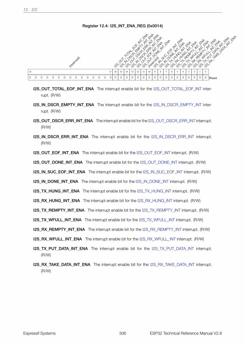
12. I2S
Register 12.4: I2S_INT_ENA_REG (0x0014)
(rese
rved)
0 0 0 0 0 0 0 0 0 0 0 0 0 0 0
31 17
I2S_O
UT_TO
TAL_
EOF_IN
T_ENA
0
16
I2S_IN
_DSCR_E
MPTY
_INT_
ENA
0
15
I2S_O
UT_DSCR_E
RR_INT_
ENA
0
14
I2S_IN
_DSCR_E
RR_INT_
ENA
0
13
I2S_O
UT_EOF_
INT_
ENA
0
12
I2S_O
UT_DONE_IN
T_ENA
0
11
(rese
rved)
0
10
I2S_IN
_SUC_E
OF_IN
T_ENA
0
9
I2S_IN
_DONE_IN
T_ENA
0
8
I2S_T
X_HUNG_IN
T_ENA
0
7
I2S_R
X_HUNG_IN
T_ENA
0
6
I2S_T
X_REM
PTY_IN
T_ENA
0
5
I2S_T
X_W
FULL
_INT_
ENA
0
4
I2S_R
X_REM
PTY_IN
T_ENA
0
3
I2S_R
X_W
FULL
_INT_
ENA
0
2
I2S_T
X_PUT_
DATA_IN
T_ENA
0
1
I2S_R
X_TA
KE_DAT
A_INT_
ENA
0
0
Reset
I2S_OUT_TOTAL_EOF_INT_ENA The interrupt enable bit for the I2S_OUT_TOTAL_EOF_INT inter-
rupt. (R/W)
I2S_IN_DSCR_EMPTY_INT_ENA The interrupt enable bit for the I2S_IN_DSCR_EMPTY_INT inter-
rupt. (R/W)
I2S_OUT_DSCR_ERR_INT_ENA The interrupt enable bit for the I2S_OUT_DSCR_ERR_INT interrupt.
(R/W)
I2S_IN_DSCR_ERR_INT_ENA The interrupt enable bit for the I2S_IN_DSCR_ERR_INT interrupt.
(R/W)
I2S_OUT_EOF_INT_ENA The interrupt enable bit for the I2S_OUT_EOF_INT interrupt. (R/W)
I2S_OUT_DONE_INT_ENA The interrupt enable bit for the I2S_OUT_DONE_INT interrupt. (R/W)
I2S_IN_SUC_EOF_INT_ENA The interrupt enable bit for the I2S_IN_SUC_EOF_INT interrupt. (R/W)
I2S_IN_DONE_INT_ENA The interrupt enable bit for the I2S_IN_DONE_INT interrupt. (R/W)
I2S_TX_HUNG_INT_ENA The interrupt enable bit for the I2S_TX_HUNG_INT interrupt. (R/W)
I2S_RX_HUNG_INT_ENA The interrupt enable bit for the I2S_RX_HUNG_INT interrupt. (R/W)
I2S_TX_REMPTY_INT_ENA The interrupt enable bit for the I2S_TX_REMPTY_INT interrupt. (R/W)
I2S_TX_WFULL_INT_ENA The interrupt enable bit for the I2S_TX_WFULL_INT interrupt. (R/W)
I2S_RX_REMPTY_INT_ENA The interrupt enable bit for the I2S_RX_REMPTY_INT interrupt. (R/W)
I2S_RX_WFULL_INT_ENA The interrupt enable bit for the I2S_RX_WFULL_INT interrupt. (R/W)
I2S_TX_PUT_DATA_INT_ENA The interrupt enable bit for the I2S_TX_PUT_DATA_INT interrupt.
(R/W)
I2S_RX_TAKE_DATA_INT_ENA The interrupt enable bit for the I2S_RX_TAKE_DATA_INT interrupt.
(R/W)
Espressif Systems 306 ESP32 Technical Reference Manual V2.8
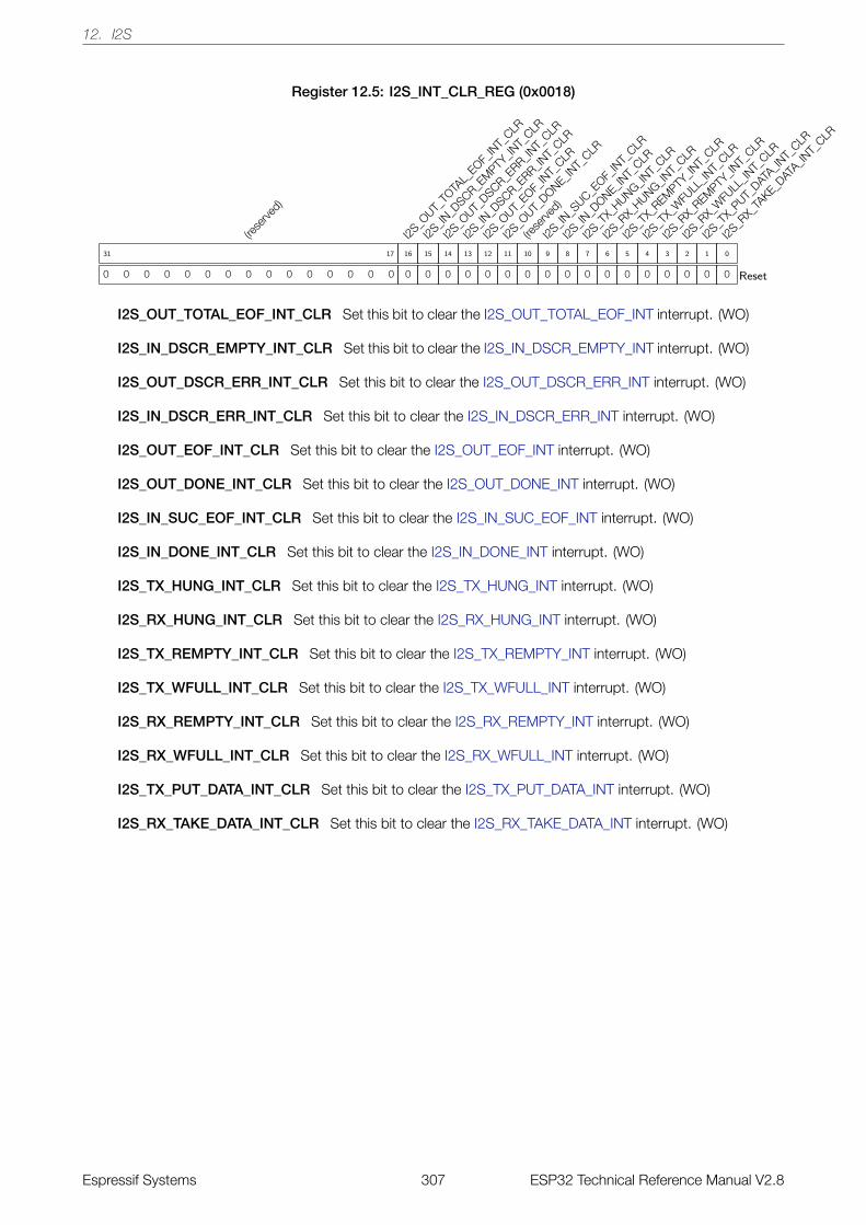
12. I2S
Register 12.5: I2S_INT_CLR_REG (0x0018)
(rese
rved)
0 0 0 0 0 0 0 0 0 0 0 0 0 0 0
31 17
I2S_O
UT_TO
TAL_
EOF_IN
T_CLR
0
16
I2S_IN
_DSCR_E
MPTY
_INT_
CLR
0
15
I2S_O
UT_DSCR_E
RR_INT_
CLR
0
14
I2S_IN
_DSCR_E
RR_INT_
CLR
0
13
I2S_O
UT_EOF_
INT_
CLR
0
12
I2S_O
UT_DONE_IN
T_CLR
0
11
(rese
rved)
0
10
I2S_IN
_SUC_E
OF_IN
T_CLR
0
9
I2S_IN
_DONE_IN
T_CLR
0
8
I2S_T
X_HUNG_IN
T_CLR
0
7
I2S_R
X_HUNG_IN
T_CLR
0
6
I2S_T
X_REM
PTY_IN
T_CLR
0
5
I2S_T
X_W
FULL
_INT_
CLR
0
4
I2S_R
X_REM
PTY_IN
T_CLR
0
3
I2S_R
X_W
FULL
_INT_
CLR
0
2
I2S_T
X_PUT_
DATA_IN
T_CLR
0
1
I2S_R
X_TA
KE_DAT
A_INT_
CLR
0
0
Reset
I2S_OUT_TOTAL_EOF_INT_CLR Set this bit to clear the I2S_OUT_TOTAL_EOF_INT interrupt. (WO)
I2S_IN_DSCR_EMPTY_INT_CLR Set this bit to clear the I2S_IN_DSCR_EMPTY_INT interrupt. (WO)
I2S_OUT_DSCR_ERR_INT_CLR Set this bit to clear the I2S_OUT_DSCR_ERR_INT interrupt. (WO)
I2S_IN_DSCR_ERR_INT_CLR Set this bit to clear the I2S_IN_DSCR_ERR_INT interrupt. (WO)
I2S_OUT_EOF_INT_CLR Set this bit to clear the I2S_OUT_EOF_INT interrupt. (WO)
I2S_OUT_DONE_INT_CLR Set this bit to clear the I2S_OUT_DONE_INT interrupt. (WO)
I2S_IN_SUC_EOF_INT_CLR Set this bit to clear the I2S_IN_SUC_EOF_INT interrupt. (WO)
I2S_IN_DONE_INT_CLR Set this bit to clear the I2S_IN_DONE_INT interrupt. (WO)
I2S_TX_HUNG_INT_CLR Set this bit to clear the I2S_TX_HUNG_INT interrupt. (WO)
I2S_RX_HUNG_INT_CLR Set this bit to clear the I2S_RX_HUNG_INT interrupt. (WO)
I2S_TX_REMPTY_INT_CLR Set this bit to clear the I2S_TX_REMPTY_INT interrupt. (WO)
I2S_TX_WFULL_INT_CLR Set this bit to clear the I2S_TX_WFULL_INT interrupt. (WO)
I2S_RX_REMPTY_INT_CLR Set this bit to clear the I2S_RX_REMPTY_INT interrupt. (WO)
I2S_RX_WFULL_INT_CLR Set this bit to clear the I2S_RX_WFULL_INT interrupt. (WO)
I2S_TX_PUT_DATA_INT_CLR Set this bit to clear the I2S_TX_PUT_DATA_INT interrupt. (WO)
I2S_RX_TAKE_DATA_INT_CLR Set this bit to clear the I2S_RX_TAKE_DATA_INT interrupt. (WO)
Espressif Systems 307 ESP32 Technical Reference Manual V2.8
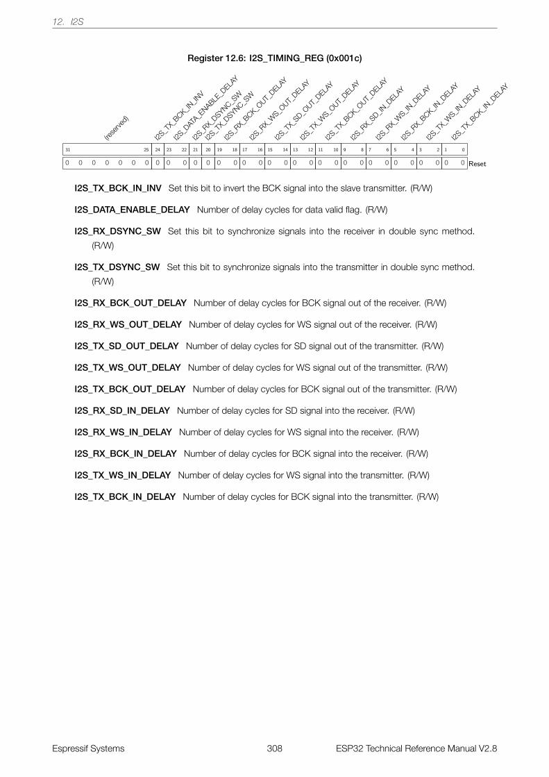
12. I2S
Register 12.6: I2S_TIMING_REG (0x001c)
(rese
rved)
0 0 0 0 0 0 0
31 25
I2S_T
X_BCK_IN
_INV
0
24
I2S_D
ATA_E
NABLE_D
ELAY
0 0
23 22
I2S_R
X_DSYNC_S
W
0
21
I2S_T
X_DSYNC_S
W
0
20
I2S_R
X_BCK_O
UT_DELA
Y
0 0
19 18
I2S_R
X_W
S_OUT_
DELAY
0 0
17 16
I2S_T
X_SD_O
UT_DELA
Y
0 0
15 14
I2S_T
X_W
S_OUT_
DELAY
0 0
13 12
I2S_T
X_BCK_O
UT_DELA
Y
0 0
11 10
I2S_R
X_SD_IN
_DELA
Y
0 0
9 8
I2S_R
X_W
S_IN_D
ELAY
0 0
7 6
I2S_R
X_BCK_IN
_DELA
Y
0 0
5 4
I2S_T
X_W
S_IN_D
ELAY
0 0
3 2
I2S_T
X_BCK_IN
_DELA
Y
0 0
1 0
Reset
I2S_TX_BCK_IN_INV Set this bit to invert the BCK signal into the slave transmitter. (R/W)
I2S_DATA_ENABLE_DELAY Number of delay cycles for data valid flag. (R/W)
I2S_RX_DSYNC_SW Set this bit to synchronize signals into the receiver in double sync method.
(R/W)
I2S_TX_DSYNC_SW Set this bit to synchronize signals into the transmitter in double sync method.
(R/W)
I2S_RX_BCK_OUT_DELAY Number of delay cycles for BCK signal out of the receiver. (R/W)
I2S_RX_WS_OUT_DELAY Number of delay cycles for WS signal out of the receiver. (R/W)
I2S_TX_SD_OUT_DELAY Number of delay cycles for SD signal out of the transmitter. (R/W)
I2S_TX_WS_OUT_DELAY Number of delay cycles for WS signal out of the transmitter. (R/W)
I2S_TX_BCK_OUT_DELAY Number of delay cycles for BCK signal out of the transmitter. (R/W)
I2S_RX_SD_IN_DELAY Number of delay cycles for SD signal into the receiver. (R/W)
I2S_RX_WS_IN_DELAY Number of delay cycles for WS signal into the receiver. (R/W)
I2S_RX_BCK_IN_DELAY Number of delay cycles for BCK signal into the receiver. (R/W)
I2S_TX_WS_IN_DELAY Number of delay cycles for WS signal into the transmitter. (R/W)
I2S_TX_BCK_IN_DELAY Number of delay cycles for BCK signal into the transmitter. (R/W)
Espressif Systems 308 ESP32 Technical Reference Manual V2.8
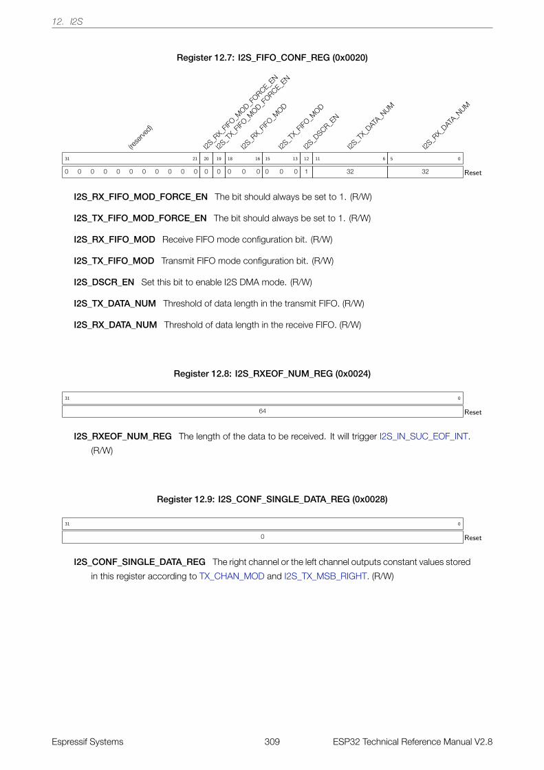
12. I2S
Register 12.7: I2S_FIFO_CONF_REG (0x0020)
(rese
rved)
0 0 0 0 0 0 0 0 0 0 0
31 21
I2S_R
X_FIF
O_MOD_F
ORCE_EN
0
20
I2S_T
X_FIF
O_MOD_F
ORCE_EN
0
19
I2S_R
X_FIF
O_MOD
0 0 0
18 16
I2S_T
X_FIF
O_MOD
0 0 0
15 13
I2S_D
SCR_EN
1
12
I2S_T
X_DAT
A_NUM
32
11 6
I2S_R
X_DAT
A_NUM
32
5 0
Reset
I2S_RX_FIFO_MOD_FORCE_EN The bit should always be set to 1. (R/W)
I2S_TX_FIFO_MOD_FORCE_EN The bit should always be set to 1. (R/W)
I2S_RX_FIFO_MOD Receive FIFO mode configuration bit. (R/W)
I2S_TX_FIFO_MOD Transmit FIFO mode configuration bit. (R/W)
I2S_DSCR_EN Set this bit to enable I2S DMA mode. (R/W)
I2S_TX_DATA_NUM Threshold of data length in the transmit FIFO. (R/W)
I2S_RX_DATA_NUM Threshold of data length in the receive FIFO. (R/W)
Register 12.8: I2S_RXEOF_NUM_REG (0x0024)
64
31 0
Reset
I2S_RXEOF_NUM_REG The length of the data to be received. It will trigger I2S_IN_SUC_EOF_INT.
(R/W)
Register 12.9: I2S_CONF_SINGLE_DATA_REG (0x0028)
0
31 0
Reset
I2S_CONF_SINGLE_DATA_REG The right channel or the left channel outputs constant values stored
in this register according to TX_CHAN_MOD and I2S_TX_MSB_RIGHT. (R/W)
Espressif Systems 309 ESP32 Technical Reference Manual V2.8
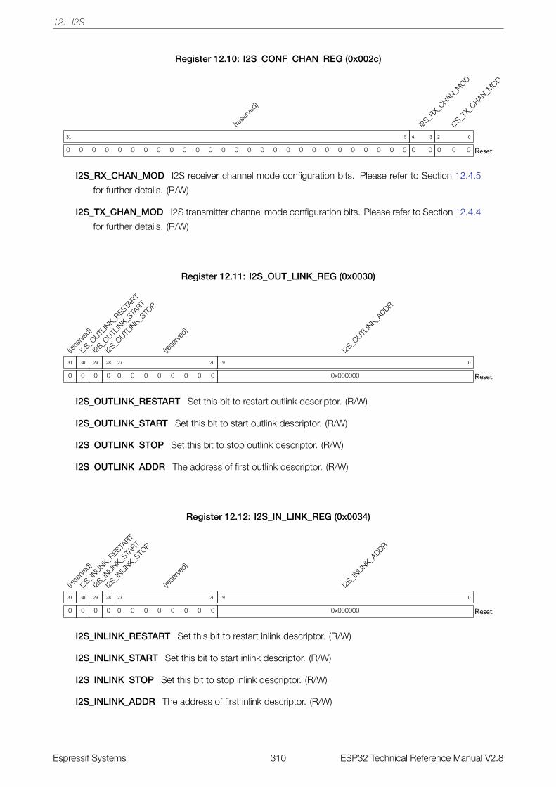
12. I2S
Register 12.10: I2S_CONF_CHAN_REG (0x002c)
(rese
rved)
0 0 0 0 0 0 0 0 0 0 0 0 0 0 0 0 0 0 0 0 0 0 0 0 0 0 0
31 5
I2S_R
X_CHAN_M
OD
0 0
4 3
I2S_T
X_CHAN_M
OD
0 0 0
2 0
Reset
I2S_RX_CHAN_MOD I2S receiver channel mode configuration bits. Please refer to Section 12.4.5
for further details. (R/W)
I2S_TX_CHAN_MOD I2S transmitter channel mode configuration bits. Please refer to Section 12.4.4
for further details. (R/W)
Register 12.11: I2S_OUT_LINK_REG (0x0030)
(rese
rved)
0
31
I2S_O
UTLIN
K_RESTA
RT
0
30
I2S_O
UTLIN
K_STA
RT
0
29
I2S_O
UTLIN
K_STO
P
0
28
(rese
rved)
0 0 0 0 0 0 0 0
27 20
I2S_O
UTLIN
K_ADDR
0x000000
19 0
Reset
I2S_OUTLINK_RESTART Set this bit to restart outlink descriptor. (R/W)
I2S_OUTLINK_START Set this bit to start outlink descriptor. (R/W)
I2S_OUTLINK_STOP Set this bit to stop outlink descriptor. (R/W)
I2S_OUTLINK_ADDR The address of first outlink descriptor. (R/W)
Register 12.12: I2S_IN_LINK_REG (0x0034)
(rese
rved)
0
31
I2S_IN
LINK_R
ESTART
0
30
I2S_IN
LINK_S
TART
0
29
I2S_IN
LINK_S
TOP
0
28
(rese
rved)
0 0 0 0 0 0 0 0
27 20
I2S_IN
LINK_A
DDR
0x000000
19 0
Reset
I2S_INLINK_RESTART Set this bit to restart inlink descriptor. (R/W)
I2S_INLINK_START Set this bit to start inlink descriptor. (R/W)
I2S_INLINK_STOP Set this bit to stop inlink descriptor. (R/W)
I2S_INLINK_ADDR The address of first inlink descriptor. (R/W)
Espressif Systems 310 ESP32 Technical Reference Manual V2.8
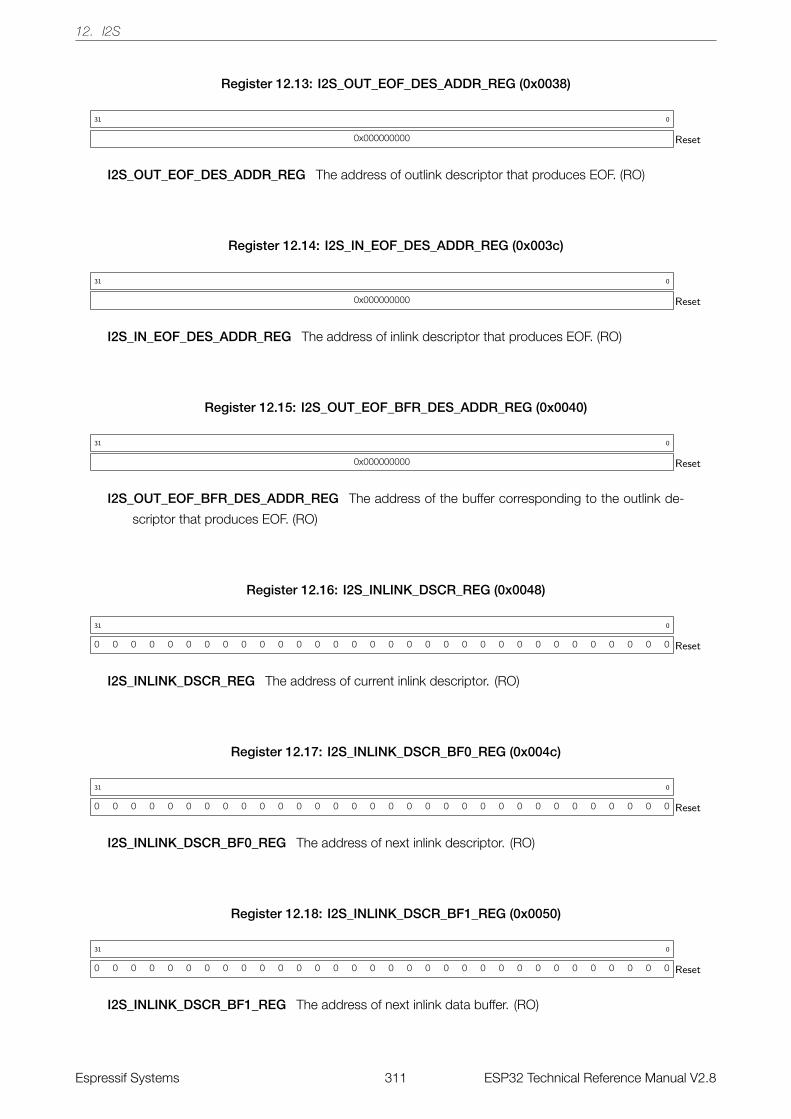
12. I2S
Register 12.13: I2S_OUT_EOF_DES_ADDR_REG (0x0038)
0x000000000
31 0
Reset
I2S_OUT_EOF_DES_ADDR_REG The address of outlink descriptor that produces EOF. (RO)
Register 12.14: I2S_IN_EOF_DES_ADDR_REG (0x003c)
0x000000000
31 0
Reset
I2S_IN_EOF_DES_ADDR_REG The address of inlink descriptor that produces EOF. (RO)
Register 12.15: I2S_OUT_EOF_BFR_DES_ADDR_REG (0x0040)
0x000000000
31 0
Reset
I2S_OUT_EOF_BFR_DES_ADDR_REG The address of the buffer corresponding to the outlink de-
scriptor that produces EOF. (RO)
Register 12.16: I2S_INLINK_DSCR_REG (0x0048)
0 0 0 0 0 0 0 0 0 0 0 0 0 0 0 0 0 0 0 0 0 0 0 0 0 0 0 0 0 0 0 0
31 0
Reset
I2S_INLINK_DSCR_REG The address of current inlink descriptor. (RO)
Register 12.17: I2S_INLINK_DSCR_BF0_REG (0x004c)
0 0 0 0 0 0 0 0 0 0 0 0 0 0 0 0 0 0 0 0 0 0 0 0 0 0 0 0 0 0 0 0
31 0
Reset
I2S_INLINK_DSCR_BF0_REG The address of next inlink descriptor. (RO)
Register 12.18: I2S_INLINK_DSCR_BF1_REG (0x0050)
0 0 0 0 0 0 0 0 0 0 0 0 0 0 0 0 0 0 0 0 0 0 0 0 0 0 0 0 0 0 0 0
31 0
Reset
I2S_INLINK_DSCR_BF1_REG The address of next inlink data buffer. (RO)
Espressif Systems 311 ESP32 Technical Reference Manual V2.8
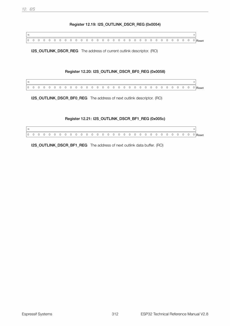
12. I2S
Register 12.19: I2S_OUTLINK_DSCR_REG (0x0054)
0 0 0 0 0 0 0 0 0 0 0 0 0 0 0 0 0 0 0 0 0 0 0 0 0 0 0 0 0 0 0 0
31 0
Reset
I2S_OUTLINK_DSCR_REG The address of current outlink descriptor. (RO)
Register 12.20: I2S_OUTLINK_DSCR_BF0_REG (0x0058)
0 0 0 0 0 0 0 0 0 0 0 0 0 0 0 0 0 0 0 0 0 0 0 0 0 0 0 0 0 0 0 0
31 0
Reset
I2S_OUTLINK_DSCR_BF0_REG The address of next outlink descriptor. (RO)
Register 12.21: I2S_OUTLINK_DSCR_BF1_REG (0x005c)
0 0 0 0 0 0 0 0 0 0 0 0 0 0 0 0 0 0 0 0 0 0 0 0 0 0 0 0 0 0 0 0
31 0
Reset
I2S_OUTLINK_DSCR_BF1_REG The address of next outlink data buffer. (RO)
Espressif Systems 312 ESP32 Technical Reference Manual V2.8
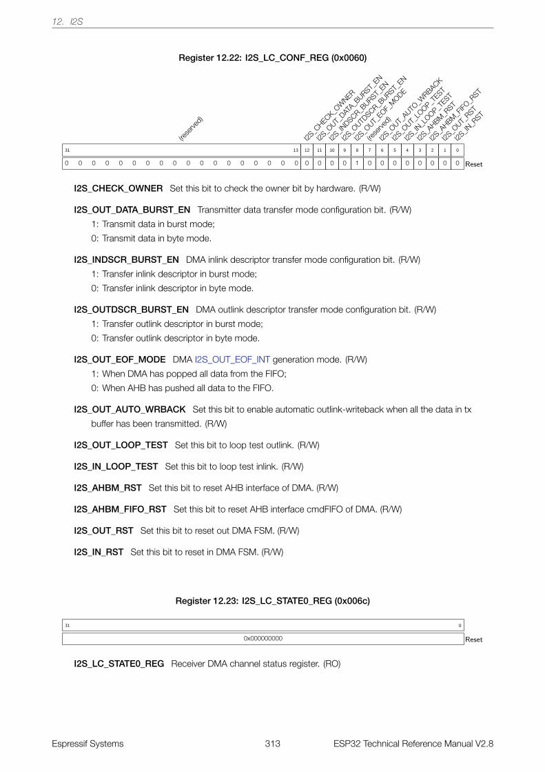
12. I2S
Register 12.22: I2S_LC_CONF_REG (0x0060)
(rese
rved)
0 0 0 0 0 0 0 0 0 0 0 0 0 0 0 0 0 0
31 13
I2S_C
HECK_OW
NER
0
12
I2S_O
UT_DAT
A_BURST_
EN
0
11
I2S_IN
DSCR_BURST_
EN
0
10
I2S_O
UTDSCR_B
URST_EN
0
9
I2S_O
UT_EOF_
MODE
1
8
(rese
rved)
0
7
I2S_O
UT_AUTO
_WRBACK
0
6
I2S_O
UT_LO
OP_TEST
0
5
I2S_IN
_LOOP_T
EST
0
4
I2S_A
HBM_R
ST
0
3
I2S_A
HBM_F
IFO_R
ST
0
2
I2S_O
UT_RST
0
1
I2S_IN
_RST
0
0
Reset
I2S_CHECK_OWNER Set this bit to check the owner bit by hardware. (R/W)
I2S_OUT_DATA_BURST_EN Transmitter data transfer mode configuration bit. (R/W)
1: Transmit data in burst mode;
0: Transmit data in byte mode.
I2S_INDSCR_BURST_EN DMA inlink descriptor transfer mode configuration bit. (R/W)
1: Transfer inlink descriptor in burst mode;
0: Transfer inlink descriptor in byte mode.
I2S_OUTDSCR_BURST_EN DMA outlink descriptor transfer mode configuration bit. (R/W)
1: Transfer outlink descriptor in burst mode;
0: Transfer outlink descriptor in byte mode.
I2S_OUT_EOF_MODE DMA I2S_OUT_EOF_INT generation mode. (R/W)
1: When DMA has popped all data from the FIFO;
0: When AHB has pushed all data to the FIFO.
I2S_OUT_AUTO_WRBACK Set this bit to enable automatic outlink-writeback when all the data in tx
buffer has been transmitted. (R/W)
I2S_OUT_LOOP_TEST Set this bit to loop test outlink. (R/W)
I2S_IN_LOOP_TEST Set this bit to loop test inlink. (R/W)
I2S_AHBM_RST Set this bit to reset AHB interface of DMA. (R/W)
I2S_AHBM_FIFO_RST Set this bit to reset AHB interface cmdFIFO of DMA. (R/W)
I2S_OUT_RST Set this bit to reset out DMA FSM. (R/W)
I2S_IN_RST Set this bit to reset in DMA FSM. (R/W)
Register 12.23: I2S_LC_STATE0_REG (0x006c)
0x000000000
31 0
Reset
I2S_LC_STATE0_REG Receiver DMA channel status register. (RO)
Espressif Systems 313 ESP32 Technical Reference Manual V2.8
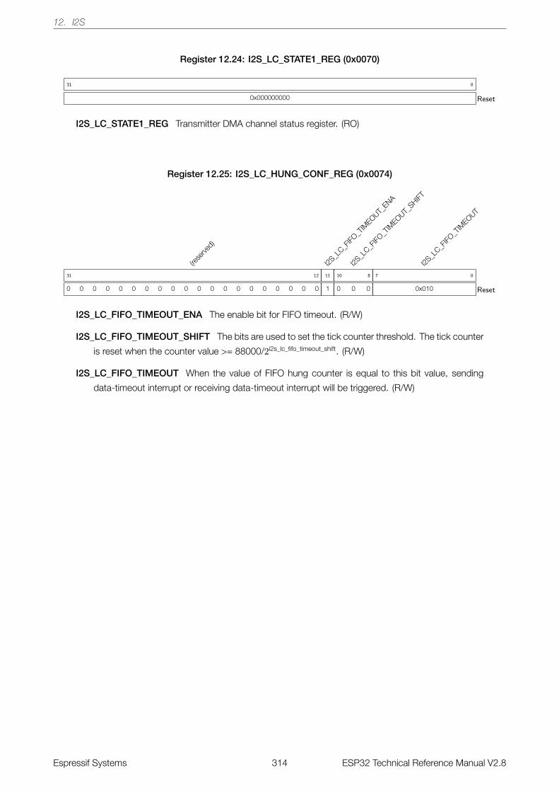
12. I2S
Register 12.24: I2S_LC_STATE1_REG (0x0070)
0x000000000
31 0
Reset
I2S_LC_STATE1_REG Transmitter DMA channel status register. (RO)
Register 12.25: I2S_LC_HUNG_CONF_REG (0x0074)
(rese
rved)
0 0 0 0 0 0 0 0 0 0 0 0 0 0 0 0 0 0 0 0
31 12
I2S_L
C_FIFO
_TIM
EOUT_ENA
1
11
I2S_L
C_FIFO
_TIM
EOUT_SHIFT
0 0 0
10 8
I2S_L
C_FIFO
_TIM
EOUT
0x010
7 0
Reset
I2S_LC_FIFO_TIMEOUT_ENA The enable bit for FIFO timeout. (R/W)
I2S_LC_FIFO_TIMEOUT_SHIFT The bits are used to set the tick counter threshold. The tick counter
is reset when the counter value >= 88000/2i2s_lc_fifo_timeout_shift. (R/W)
I2S_LC_FIFO_TIMEOUT When the value of FIFO hung counter is equal to this bit value, sending
data-timeout interrupt or receiving data-timeout interrupt will be triggered. (R/W)
Espressif Systems 314 ESP32 Technical Reference Manual V2.8
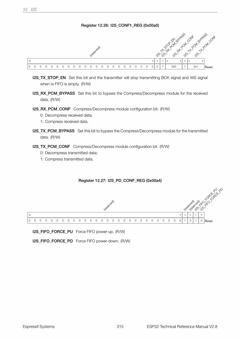
12. I2S
Register 12.26: I2S_CONF1_REG (0x00a0)
(rese
rved)
0 0 0 0 0 0 0 0 0 0 0 0 0 0 0 0 0 0 0 0 0 0 0
31 9
I2S_T
X_STO
P_EN
0
8
I2S_R
X_PCM
_BYPA
SS
1
7
I2S_R
X_PCM
_CONF
0x0
6 4
I2S_T
X_PCM
_BYPA
SS
1
3
I2S_T
X_PCM
_CONF
0x1
2 0
Reset
I2S_TX_STOP_EN Set this bit and the transmitter will stop transmitting BCK signal and WS signal
when tx FIFO is empty. (R/W)
I2S_RX_PCM_BYPASS Set this bit to bypass the Compress/Decompress module for the received
data. (R/W)
I2S_RX_PCM_CONF Compress/Decompress module configuration bit. (R/W)
0: Decompress received data;
1: Compress received data.
I2S_TX_PCM_BYPASS Set this bit to bypass the Compress/Decompress module for the transmitted
data. (R/W)
I2S_TX_PCM_CONF Compress/Decompress module configuration bit. (R/W)
0: Decompress transmitted data;
1: Compress transmitted data.
Register 12.27: I2S_PD_CONF_REG (0x00a4)
(rese
rved)
0 0 0 0 0 0 0 0 0 0 0 0 0 0 0 0 0 0 0 0 0 0 0 0 0 0 0 0
31 4
(rese
rved)
1
3
(rese
rved)
0
2
I2S_F
IFO_F
ORCE_PU
1
1
I2S_F
IFO_F
ORCE_PD
0
0
Reset
I2S_FIFO_FORCE_PU Force FIFO power-up. (R/W)
I2S_FIFO_FORCE_PD Force FIFO power-down. (R/W)
Espressif Systems 315 ESP32 Technical Reference Manual V2.8
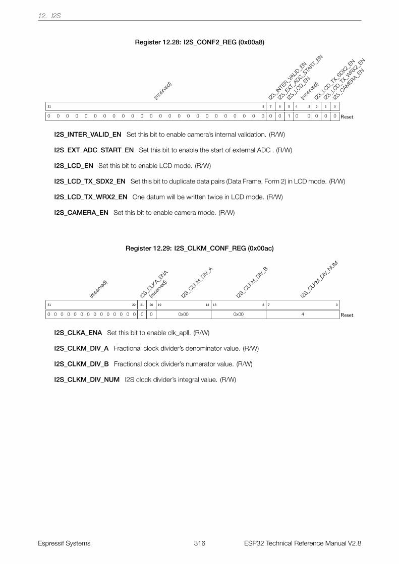
12. I2S
Register 12.28: I2S_CONF2_REG (0x00a8)
(rese
rved)
0 0 0 0 0 0 0 0 0 0 0 0 0 0 0 0 0 0 0 0 0 0 0 0
31 8
I2S_IN
TER_V
ALID_E
N
0
7
I2S_E
XT_A
DC_STA
RT_EN
0
6
I2S_L
CD_EN
1
5
(rese
rved)
0 0
4 3
I2S_L
CD_TX_
SDX2_E
N
0
2
I2S_L
CD_TX_
WRX2
_EN
0
1
I2S_C
AMERA_E
N
0
0
Reset
I2S_INTER_VALID_EN Set this bit to enable camera’s internal validation. (R/W)
I2S_EXT_ADC_START_EN Set this bit to enable the start of external ADC . (R/W)
I2S_LCD_EN Set this bit to enable LCD mode. (R/W)
I2S_LCD_TX_SDX2_EN Set this bit to duplicate data pairs (Data Frame, Form 2) in LCD mode. (R/W)
I2S_LCD_TX_WRX2_EN One datum will be written twice in LCD mode. (R/W)
I2S_CAMERA_EN Set this bit to enable camera mode. (R/W)
Register 12.29: I2S_CLKM_CONF_REG (0x00ac)
(rese
rved)
0 0 0 0 0 0 0 0 0 0 0 0 0 0
31 22
I2S_C
LKA_E
NA
0
21
(rese
rved)
0
20
I2S_C
LKM
_DIV_A
0x00
19 14
I2S_C
LKM
_DIV_B
0x00
13 8
I2S_C
LKM
_DIV_N
UM
4
7 0
Reset
I2S_CLKA_ENA Set this bit to enable clk_apll. (R/W)
I2S_CLKM_DIV_A Fractional clock divider’s denominator value. (R/W)
I2S_CLKM_DIV_B Fractional clock divider’s numerator value. (R/W)
I2S_CLKM_DIV_NUM I2S clock divider’s integral value. (R/W)
Espressif Systems 316 ESP32 Technical Reference Manual V2.8
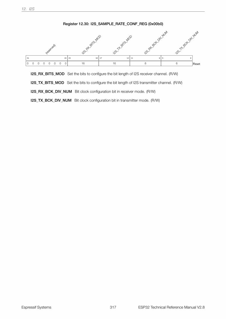
12. I2S
Register 12.30: I2S_SAMPLE_RATE_CONF_REG (0x00b0)
(rese
rved)
0 0 0 0 0 0 0 0
31 24
I2S_R
X_BITS
_MOD
16
23 18
I2S_T
X_BITS
_MOD
16
17 12
I2S_R
X_BCK_D
IV_NUM
6
11 6
I2S_T
X_BCK_D
IV_NUM
6
5 0
Reset
I2S_RX_BITS_MOD Set the bits to configure the bit length of I2S receiver channel. (R/W)
I2S_TX_BITS_MOD Set the bits to configure the bit length of I2S transmitter channel. (R/W)
I2S_RX_BCK_DIV_NUM Bit clock configuration bit in receiver mode. (R/W)
I2S_TX_BCK_DIV_NUM Bit clock configuration bit in transmitter mode. (R/W)
Espressif Systems 317 ESP32 Technical Reference Manual V2.8
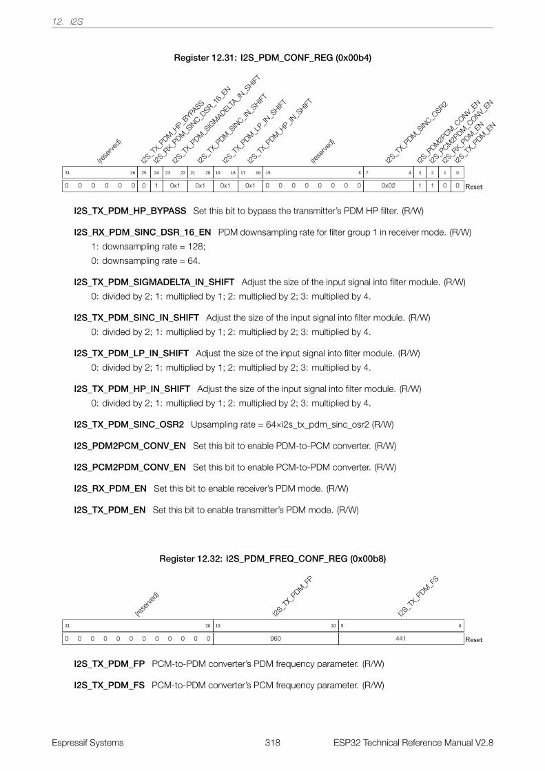
12. I2S
Register 12.31: I2S_PDM_CONF_REG (0x00b4)
(rese
rved)
0 0 0 0 0 0
31 26
I2S_T
X_PDM
_HP_B
YPASS
0
25
I2S_R
X_PDM
_SIN
C_DSR_1
6_EN
1
24
I2S_T
X_PDM
_SIG
MADELT
A_IN_S
HIFT
0x1
23 22
I2S_T
X_PDM
_SIN
C_IN_S
HIFT
0x1
21 20
I2S_T
X_PDM
_LP_IN
_SHIFT
0x1
19 18
I2S_T
X_PDM
_HP_IN
_SHIFT
0x1
17 16
(rese
rved)
0 0 0 0 0 0 0 0
15 8
I2S_T
X_PDM
_SIN
C_OSR2
0x02
7 4
I2S_P
DM2P
CM_C
ONV_EN
1
3
I2S_P
CM2P
DM_C
ONV_EN
1
2
I2S_R
X_PDM
_EN
0
1
I2S_T
X_PDM
_EN
0
0
Reset
I2S_TX_PDM_HP_BYPASS Set this bit to bypass the transmitter’s PDM HP filter. (R/W)
I2S_RX_PDM_SINC_DSR_16_EN PDM downsampling rate for filter group 1 in receiver mode. (R/W)
1: downsampling rate = 128;
0: downsampling rate = 64.
I2S_TX_PDM_SIGMADELTA_IN_SHIFT Adjust the size of the input signal into filter module. (R/W)
0: divided by 2; 1: multiplied by 1; 2: multiplied by 2; 3: multiplied by 4.
I2S_TX_PDM_SINC_IN_SHIFT Adjust the size of the input signal into filter module. (R/W)
0: divided by 2; 1: multiplied by 1; 2: multiplied by 2; 3: multiplied by 4.
I2S_TX_PDM_LP_IN_SHIFT Adjust the size of the input signal into filter module. (R/W)
0: divided by 2; 1: multiplied by 1; 2: multiplied by 2; 3: multiplied by 4.
I2S_TX_PDM_HP_IN_SHIFT Adjust the size of the input signal into filter module. (R/W)
0: divided by 2; 1: multiplied by 1; 2: multiplied by 2; 3: multiplied by 4.
I2S_TX_PDM_SINC_OSR2 Upsampling rate = 64×i2s_tx_pdm_sinc_osr2 (R/W)
I2S_PDM2PCM_CONV_EN Set this bit to enable PDM-to-PCM converter. (R/W)
I2S_PCM2PDM_CONV_EN Set this bit to enable PCM-to-PDM converter. (R/W)
I2S_RX_PDM_EN Set this bit to enable receiver’s PDM mode. (R/W)
I2S_TX_PDM_EN Set this bit to enable transmitter’s PDM mode. (R/W)
Register 12.32: I2S_PDM_FREQ_CONF_REG (0x00b8)
(rese
rved)
0 0 0 0 0 0 0 0 0 0 0 0
31 20
I2S_T
X_PDM
_FP
960
19 10
I2S_T
X_PDM
_FS
441
9 0
Reset
I2S_TX_PDM_FP PCM-to-PDM converter’s PDM frequency parameter. (R/W)
I2S_TX_PDM_FS PCM-to-PDM converter’s PCM frequency parameter. (R/W)
Espressif Systems 318 ESP32 Technical Reference Manual V2.8
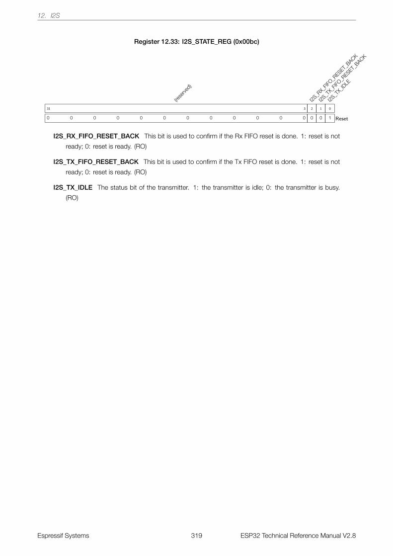
12. I2S
Register 12.33: I2S_STATE_REG (0x00bc)
(rese
rved)
0 0 0 0 0 0 0 0 0 0 0 0
31 3
I2S_R
X_FIF
O_RESET_
BACK
0
2
I2S_T
X_FIF
O_RESET_
BACK
0
1
I2S_T
X_ID
LE
1
0
Reset
I2S_RX_FIFO_RESET_BACK This bit is used to confirm if the Rx FIFO reset is done. 1: reset is not
ready; 0: reset is ready. (RO)
I2S_TX_FIFO_RESET_BACK This bit is used to confirm if the Tx FIFO reset is done. 1: reset is not
ready; 0: reset is ready. (RO)
I2S_TX_IDLE The status bit of the transmitter. 1: the transmitter is idle; 0: the transmitter is busy.
(RO)
Espressif Systems 319 ESP32 Technical Reference Manual V2.8
13. UART CONTROLLERS
13. UART Controllers
13.1 Overview
Embedded applications often require a simple method of exchanging data between devices that need minimal
system resources. The Universal Asynchronous Receiver/Transmitter (UART) is one such standard that can
realize a flexible full-duplex data exchange among different devices. The three UART controllers available on a
chip are compatible with UART-enabled devices from various manufacturers. The UART can also carry out an
IrDA (Infrared Data Exchange), or function as an RS-485 modem.
All UART controllers integrated in the ESP32 feature an identical set of registers for ease of programming and
flexibility. In this documentation, these controllers are referred to as UARTn, where n = 0, 1, and 2, referring to
UART0, UART1, and UART2, respectively.
13.2 UART Features
The UART modules have the following main features:
• Programmable baud rate
• 1024 x 8-bit RAM shared by three UART transmit-FIFOs and receive-FIFOs
• Supports input baud rate self-check
• Supports 5/6/7/8 bits of data length
• Supports 1/1.5/2/3/4 STOP bits
• Supports parity bit
• Supports RS485 Protocol
• Supports IrDA Protocol
• Supports DMA to communicate data in high speed
• Supports UART wake-up
• Supports both software and hardware flow control
13.3 Functional Description
13.3.1 Introduction
UART is a character-oriented data link that can be used to achieve communication between two devices. The
asynchronous mode of transmission means that it is not necessary to add clocking information to the data being
sent. This, in turn, requires that the data rate, STOP bits, parity, etc., be identical at the transmitting and receiving
end for the devices to communicate successfully.
A typical UART frame begins with a START bit, followed by a “character” and an optional parity bit for error
detection, and it ends with a STOP condition. The UART controllers available on the ESP32 provide hardware
support for multiple lengths of data and STOP bits. In addition, the controllers support both software and
hardware flow control, as well as DMA, for seamless high-speed data transfer. This allows the developer to
employ multiple UART ports in the system with minimal software overhead.
Espressif Systems 320 ESP32 Technical Reference Manual V2.8
13. UART CONTROLLERS
13.3.2 UART Architecture
Figure 78: UART Basic Structure
Figure 78 shows the basic block diagram of the UART controller. The UART block can derive its clock from two
sources: the 80-MHz APB_CLK, or the reference clock REF_TICK (please refer to Chapter Reset and Clock for
more details). These two clock sources can be selected by configuring UART_TICK_REF_ALWAYS_ON.
Then, a divider in the clock path divides the selected clock source to generate clock signals that drive the UART
module. UART_CLKDIV_REG contains the clock divider value in two parts — UART_CLKDIV (integral part) and
UART_CLKDIV_FRAG (decimal part).
The UART controller can be further broken down into two functional blocks — the transmit block and the receive
block.
The transmit block contains a transmit-FIFO buffer, which buffers data awaiting to be transmitted. Software can
write Tx_FIFO via APB, and transmit data into Tx_FIFO via DMA. Tx_FIFO_Ctrl is used to control read- and
write-access to the Tx_FIFO. When Tx_FIFO is not null, Tx_FSM reads data via Tx_FIFO_Ctrl, and transmits data
out according to the set frame format. The outgoing bit stream can be inverted by appropriately configuring the
register UART_TXD_INV.
The receive-block contains a receive-FIFO buffer, which buffers incoming data awaiting to be processed. The
input bit stream, rxd_in, is fed to the UART controller. Negation of the input stream can be controlled by
configuring the UART_RXD_INV register. Baudrate_Detect measures the baud rate of the input signal by
measuring the minimum pulse width of the input bit stream. Start_Detect is used to detect a START bit in a frame
of incoming data. After detecting the START bit, RX_FSM stores data retrieved from the received frame into
Rx_FIFO through Rx_FIFO_Ctrl.
Software can read data in the Rx_FIFO through the APB. In order to free the CPU from engaging in data transfer
operations, the DMA can be configured for sending or receiving data.
HW_Flow_Ctrl is able to control the data flow of rxd_in and txd_out through standard UART RTS and CTS flow
control signals (rtsn_out and ctsn_in). SW_Flow_Ctrl controls the data flow by inserting special characters in the
incoming and outgoing data flow. When UART is in Light-sleep mode (refer to Chapter Low-Power
Management), Wakeup_Ctrl will start counting pulses in rxd_in. If the number of pulses is greater than
UART_ACTIVE_THRESHOLD, a wake_up signal will be generated and sent to RTC. RTC will then wake up the
Espressif Systems 321 ESP32 Technical Reference Manual V2.8

13. UART CONTROLLERS
UART controller.
13.3.3 UART RAM
Figure 79: UART shared RAM
Three UART controllers share a 1024 x 8-bit RAM space. As illustrated in Figure 79, RAM is allocated in different
blocks. One block holds 128 x 8-bit data. Figure 79 illustrates the default RAM allocated to Tx_FIFO and
Rx_FIFO of the three UART controllers. Tx_FIFO of UARTn can be extended by setting UARTn_TX_SIZE, while
Rx_FIFO of UARTn can be extended by setting UARTn_RX_SIZE.
NOTICE: Extending the FIFO space of a UART controller may take up the FIFO space of another UART
controller.
If none of the UART controllers is active, setting UART_MEM_PD, UART1_MEM_PD, and UART2_MEM_PD can
prompt the RAM to enter low-power mode.
In UART0, bit UART_TXFIFO_RST and bit UART_RXFIFO_RST can be set to reset Tx_FIFO or Rx_FIFO,
respectively. In UART1, bit UART1_TXFIFO_RST and bit UART1_RXFIFO_RST can be set to reset Tx_FIFO or
Rx_FIFO, respectively.
Note:
UART2 doesn’t have any register to reset Tx_FIFO or Rx_FIFO, and the UART1_TXFIFO_RST and UART1_RXFIFO_RST
in UART1 may impact the functioning of UART2. Therefore, these 2 registers in UART1 should only be used when the
Tx_FIFO and Rx_FIFO in UART2 do not have any data.
13.3.4 Baud Rate Detection
Setting UART_AUTOBAUD_EN for a UART controller will enable the baud rate detection function. The
Baudrate_Detect block shown in Figure 78 can filter glitches with a pulse width lower than
UART_GLITCH_FILT.
In order to use the baud rate detection feature, some random data should be sent to the receiver before starting
Espressif Systems 322 ESP32 Technical Reference Manual V2.8
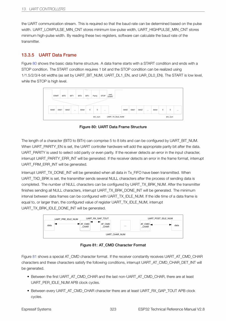
13. UART CONTROLLERS
the UART communication stream. This is required so that the baud rate can be determined based on the pulse
width. UART_LOWPULSE_MIN_CNT stores minimum low-pulse width, UART_HIGHPULSE_MIN_CNT stores
minimum high-pulse width. By reading these two registers, software can calculate the baud rate of the
transmitter.
13.3.5 UART Data Frame
Figure 80 shows the basic data frame structure. A data frame starts with a START condition and ends with a
STOP condition. The START condition requires 1 bit and the STOP condition can be realized using
1/1.5/2/3/4-bit widths (as set by UART_BIT_NUM, UART_DL1_EN, and UAR_DL0_EN). The START is low level,
while the STOP is high level.
Figure 80: UART Data Frame Structure
The length of a character (BIT0 to BITn) can comprise 5 to 8 bits and can be configured by UART_BIT_NUM.
When UART_PARITY_EN is set, the UART controller hardware will add the appropriate parity bit after the data.
UART_PARITY is used to select odd parity or even parity. If the receiver detects an error in the input character,
interrupt UART_PARITY_ERR_INT will be generated. If the receiver detects an error in the frame format, interrupt
UART_FRM_ERR_INT will be generated.
Interrupt UART_TX_DONE_INT will be generated when all data in Tx_FIFO have been transmitted. When
UART_TXD_BRK is set, the transmitter sends several NULL characters after the process of sending data is
completed. The number of NULL characters can be configured by UART_TX_BRK_NUM. After the transmitter
finishes sending all NULL characters, interrupt UART_TX_BRK_DONE_INT will be generated. The minimum
interval between data frames can be configured with UART_TX_IDLE_NUM. If the idle time of a data frame is
equal to, or larger than, the configured value of register UART_TX_IDLE_NUM, interrupt
UART_TX_BRK_IDLE_DONE_INT will be generated.
Figure 81: AT_CMD Character Format
Figure 81 shows a special AT_CMD character format. If the receiver constantly receives UART_AT_CMD_CHAR
characters and these characters satisfy the following conditions, interrupt UART_AT_CMD_CHAR_DET_INT will
be generated.
• Between the first UART_AT_CMD_CHAR and the last non-UART_AT_CMD_CHAR, there are at least
UART_PER_IDLE_NUM APB clock cycles.
• Between every UART_AT_CMD_CHAR character there are at least UART_RX_GAP_TOUT APB clock
cycles.
Espressif Systems 323 ESP32 Technical Reference Manual V2.8
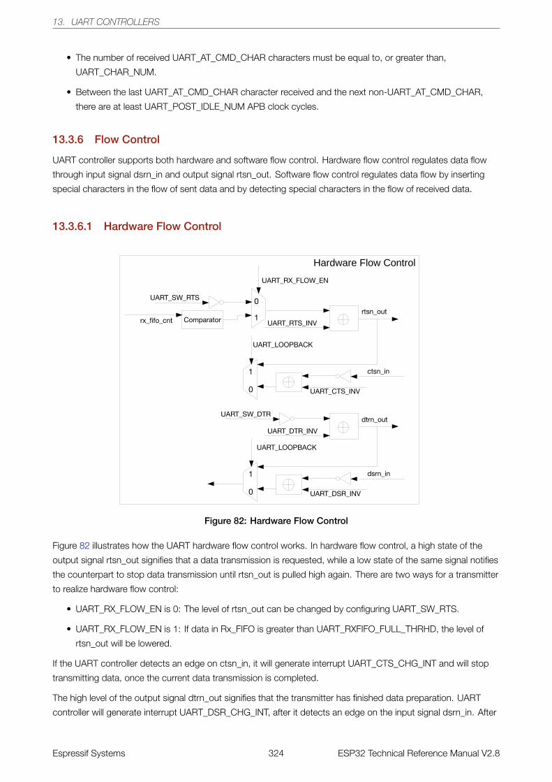
13. UART CONTROLLERS
• The number of received UART_AT_CMD_CHAR characters must be equal to, or greater than,
UART_CHAR_NUM.
• Between the last UART_AT_CMD_CHAR character received and the next non-UART_AT_CMD_CHAR,
there are at least UART_POST_IDLE_NUM APB clock cycles.
13.3.6 Flow Control
UART controller supports both hardware and software flow control. Hardware flow control regulates data flow
through input signal dsrn_in and output signal rtsn_out. Software flow control regulates data flow by inserting
special characters in the flow of sent data and by detecting special characters in the flow of received data.
13.3.6.1 Hardware Flow Control
Figure 82: Hardware Flow Control
Figure 82 illustrates how the UART hardware flow control works. In hardware flow control, a high state of the
output signal rtsn_out signifies that a data transmission is requested, while a low state of the same signal notifies
the counterpart to stop data transmission until rtsn_out is pulled high again. There are two ways for a transmitter
to realize hardware flow control:
• UART_RX_FLOW_EN is 0: The level of rtsn_out can be changed by configuring UART_SW_RTS.
• UART_RX_FLOW_EN is 1: If data in Rx_FIFO is greater than UART_RXFIFO_FULL_THRHD, the level of
rtsn_out will be lowered.
If the UART controller detects an edge on ctsn_in, it will generate interrupt UART_CTS_CHG_INT and will stop
transmitting data, once the current data transmission is completed.
The high level of the output signal dtrn_out signifies that the transmitter has finished data preparation. UART
controller will generate interrupt UART_DSR_CHG_INT, after it detects an edge on the input signal dsrn_in. After
Espressif Systems 324 ESP32 Technical Reference Manual V2.8
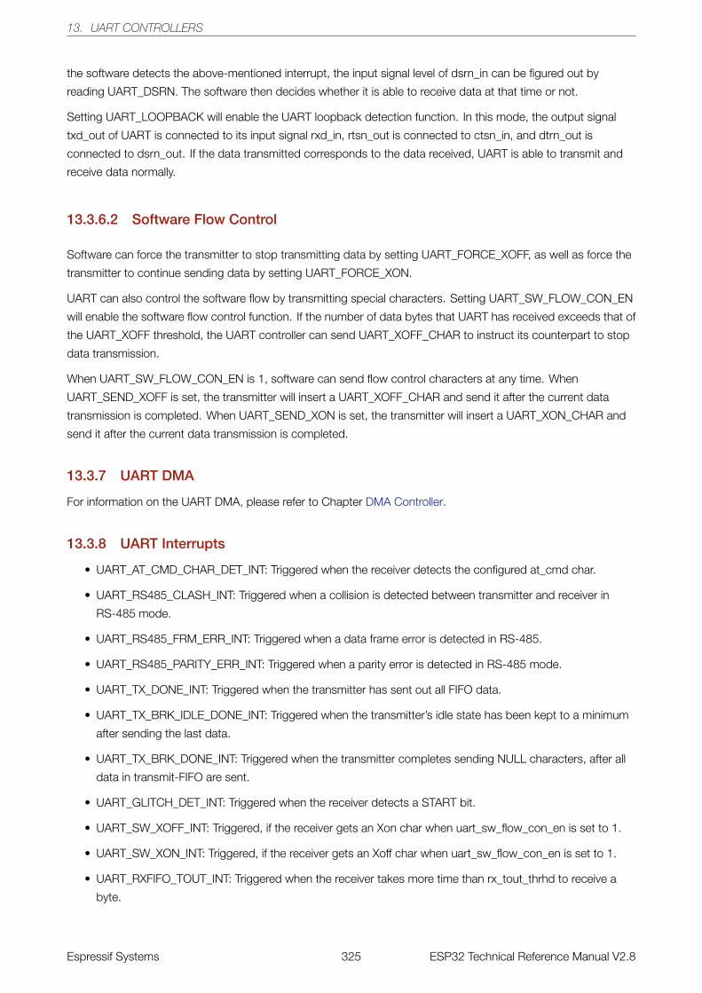
13. UART CONTROLLERS
the software detects the above-mentioned interrupt, the input signal level of dsrn_in can be figured out by
reading UART_DSRN. The software then decides whether it is able to receive data at that time or not.
Setting UART_LOOPBACK will enable the UART loopback detection function. In this mode, the output signal
txd_out of UART is connected to its input signal rxd_in, rtsn_out is connected to ctsn_in, and dtrn_out is
connected to dsrn_out. If the data transmitted corresponds to the data received, UART is able to transmit and
receive data normally.
13.3.6.2 Software Flow Control
Software can force the transmitter to stop transmitting data by setting UART_FORCE_XOFF, as well as force the
transmitter to continue sending data by setting UART_FORCE_XON.
UART can also control the software flow by transmitting special characters. Setting UART_SW_FLOW_CON_EN
will enable the software flow control function. If the number of data bytes that UART has received exceeds that of
the UART_XOFF threshold, the UART controller can send UART_XOFF_CHAR to instruct its counterpart to stop
data transmission.
When UART_SW_FLOW_CON_EN is 1, software can send flow control characters at any time. When
UART_SEND_XOFF is set, the transmitter will insert a UART_XOFF_CHAR and send it after the current data
transmission is completed. When UART_SEND_XON is set, the transmitter will insert a UART_XON_CHAR and
send it after the current data transmission is completed.
13.3.7 UART DMA
For information on the UART DMA, please refer to Chapter DMA Controller.
13.3.8 UART Interrupts
• UART_AT_CMD_CHAR_DET_INT: Triggered when the receiver detects the configured at_cmd char.
• UART_RS485_CLASH_INT: Triggered when a collision is detected between transmitter and receiver in
RS-485 mode.
• UART_RS485_FRM_ERR_INT: Triggered when a data frame error is detected in RS-485.
• UART_RS485_PARITY_ERR_INT: Triggered when a parity error is detected in RS-485 mode.
• UART_TX_DONE_INT: Triggered when the transmitter has sent out all FIFO data.
• UART_TX_BRK_IDLE_DONE_INT: Triggered when the transmitter’s idle state has been kept to a minimum
after sending the last data.
• UART_TX_BRK_DONE_INT: Triggered when the transmitter completes sending NULL characters, after all
data in transmit-FIFO are sent.
• UART_GLITCH_DET_INT: Triggered when the receiver detects a START bit.
• UART_SW_XOFF_INT: Triggered, if the receiver gets an Xon char when uart_sw_flow_con_en is set to 1.
• UART_SW_XON_INT: Triggered, if the receiver gets an Xoff char when uart_sw_flow_con_en is set to 1.
• UART_RXFIFO_TOUT_INT: Triggered when the receiver takes more time than rx_tout_thrhd to receive a
byte.
Espressif Systems 325 ESP32 Technical Reference Manual V2.8
13. UART CONTROLLERS
• UART_BRK_DET_INT: Triggered when the receiver detects a 0 level after the STOP bit.
• UART_CTS_CHG_INT: Triggered when the receiver detects an edge change of the CTSn signal.
• UART_DSR_CHG_INT: Triggered when the receiver detects an edge change of the DSRn signal.
• UART_RXFIFO_OVF_INT: Triggered when the receiver gets more data than the FIFO can store.
• UART_FRM_ERR_INT: Triggered when the receiver detects a data frame error .
• UART_PARITY_ERR_INT: Triggered when the receiver detects a parity error in the data.
• UART_TXFIFO_EMPTY_INT: Triggered when the amount of data in the transmit-FIFO is less than what
tx_mem_cnttxfifo_cnt specifies.
• UART_RXFIFO_FULL_INT: Triggered when the receiver gets more data than what (rx_flow_thrhd_h3,
rx_flow_thrhd) specifies.
13.3.9 UCHI Interrupts
• UHCI_SEND_A_REG_Q_INT: When using the always_send registers to send a series of short packets, this
is triggered when DMA has sent a short packet.
• UHCI_SEND_S_REG_Q_INT: When using the single_send registers to send a series of short packets, this is
triggered when DMA has sent a short packet.
• UHCI_OUT_TOTAL_EOF_INT: Triggered when all data have been sent.
• UHCI_OUTLINK_EOF_ERR_INT: Triggered when there are some errors in EOF in the outlink descriptor.
• UHCI_IN_DSCR_EMPTY_INT: Triggered when there are not enough inlinks for DMA.
• UHCI_OUT_DSCR_ERR_INT: Triggered when there are some errors in the inlink descriptor.
• UHCI_IN_DSCR_ERR_INT: Triggered when there are some errors in the outlink descriptor.
• UHCI_OUT_EOF_INT: Triggered when the current descriptor’s EOF bit is 1.
• UHCI_OUT_DONE_INT: Triggered when an outlink descriptor is completed.
• UHCI_IN_ERR_EOF_INT: Triggered when there are some errors in EOF in the inlink descriptor.
• UHCI_IN_SUC_EOF_INT: Triggered when a data packet has been received.
• UHCI_IN_DONE_INT: Triggered when an inlink descriptor has been completed.
• UHCI_TX_HUNG_INT: Triggered when DMA takes much time to read data from RAM.
• UHCI_RX_HUNG_INT: Triggered when DMA takes much time to receive data .
• UHCI_TX_START_INT: Triggered when DMA detects a separator char.
• UHCI_RX_START_INT: Triggered when a separator char has been sent.
13.4 Register Summary
Name Description UART0 UART1 UART2 Acc
Configuration registers
UART_CONF0_REG Configuration register 0 0x3FF40020 0x3FF50020 0x3FF6E020 R/W
Espressif Systems 326 ESP32 Technical Reference Manual V2.8
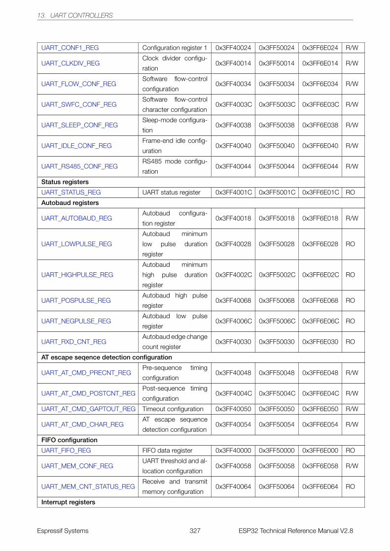
13. UART CONTROLLERS
UART_CONF1_REG Configuration register 1 0x3FF40024 0x3FF50024 0x3FF6E024 R/W
UART_CLKDIV_REGClock divider configu-
ration0x3FF40014 0x3FF50014 0x3FF6E014 R/W
UART_FLOW_CONF_REGSoftware flow-control
configuration0x3FF40034 0x3FF50034 0x3FF6E034 R/W
UART_SWFC_CONF_REGSoftware flow-control
character configuration0x3FF4003C 0x3FF5003C 0x3FF6E03C R/W
UART_SLEEP_CONF_REGSleep-mode configura-
tion0x3FF40038 0x3FF50038 0x3FF6E038 R/W
UART_IDLE_CONF_REGFrame-end idle config-
uration0x3FF40040 0x3FF50040 0x3FF6E040 R/W
UART_RS485_CONF_REGRS485 mode configu-
ration0x3FF40044 0x3FF50044 0x3FF6E044 R/W
Status registers
UART_STATUS_REG UART status register 0x3FF4001C 0x3FF5001C 0x3FF6E01C RO
Autobaud registers
UART_AUTOBAUD_REGAutobaud configura-
tion register0x3FF40018 0x3FF50018 0x3FF6E018 R/W
UART_LOWPULSE_REG
Autobaud minimum
low pulse duration
register
0x3FF40028 0x3FF50028 0x3FF6E028 RO
UART_HIGHPULSE_REG
Autobaud minimum
high pulse duration
register
0x3FF4002C 0x3FF5002C 0x3FF6E02C RO
UART_POSPULSE_REGAutobaud high pulse
register0x3FF40068 0x3FF50068 0x3FF6E068 RO
UART_NEGPULSE_REGAutobaud low pulse
register0x3FF4006C 0x3FF5006C 0x3FF6E06C RO
UART_RXD_CNT_REGAutobaud edge change
count register0x3FF40030 0x3FF50030 0x3FF6E030 RO
AT escape seqence detection configuration
UART_AT_CMD_PRECNT_REGPre-sequence timing
configuration0x3FF40048 0x3FF50048 0x3FF6E048 R/W
UART_AT_CMD_POSTCNT_REGPost-sequence timing
configuration0x3FF4004C 0x3FF5004C 0x3FF6E04C R/W
UART_AT_CMD_GAPTOUT_REG Timeout configuration 0x3FF40050 0x3FF50050 0x3FF6E050 R/W
UART_AT_CMD_CHAR_REGAT escape sequence
detection configuration0x3FF40054 0x3FF50054 0x3FF6E054 R/W
FIFO configuration
UART_FIFO_REG FIFO data register 0x3FF40000 0x3FF50000 0x3FF6E000 RO
UART_MEM_CONF_REGUART threshold and al-
location configuration0x3FF40058 0x3FF50058 0x3FF6E058 R/W
UART_MEM_CNT_STATUS_REGReceive and transmit
memory configuration0x3FF40064 0x3FF50064 0x3FF6E064 RO
Interrupt registers
Espressif Systems 327 ESP32 Technical Reference Manual V2.8
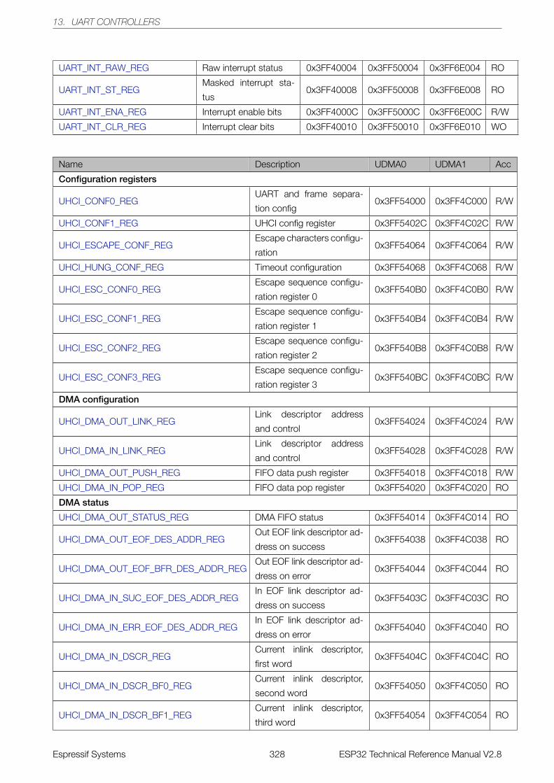
13. UART CONTROLLERS
UART_INT_RAW_REG Raw interrupt status 0x3FF40004 0x3FF50004 0x3FF6E004 RO
UART_INT_ST_REGMasked interrupt sta-
tus0x3FF40008 0x3FF50008 0x3FF6E008 RO
UART_INT_ENA_REG Interrupt enable bits 0x3FF4000C 0x3FF5000C 0x3FF6E00C R/W
UART_INT_CLR_REG Interrupt clear bits 0x3FF40010 0x3FF50010 0x3FF6E010 WO
Name Description UDMA0 UDMA1 Acc
Configuration registers
UHCI_CONF0_REGUART and frame separa-
tion config0x3FF54000 0x3FF4C000 R/W
UHCI_CONF1_REG UHCI config register 0x3FF5402C 0x3FF4C02C R/W
UHCI_ESCAPE_CONF_REGEscape characters configu-
ration0x3FF54064 0x3FF4C064 R/W
UHCI_HUNG_CONF_REG Timeout configuration 0x3FF54068 0x3FF4C068 R/W
UHCI_ESC_CONF0_REGEscape sequence configu-
ration register 00x3FF540B0 0x3FF4C0B0 R/W
UHCI_ESC_CONF1_REGEscape sequence configu-
ration register 10x3FF540B4 0x3FF4C0B4 R/W
UHCI_ESC_CONF2_REGEscape sequence configu-
ration register 20x3FF540B8 0x3FF4C0B8 R/W
UHCI_ESC_CONF3_REGEscape sequence configu-
ration register 30x3FF540BC 0x3FF4C0BC R/W
DMA configuration
UHCI_DMA_OUT_LINK_REGLink descriptor address
and control0x3FF54024 0x3FF4C024 R/W
UHCI_DMA_IN_LINK_REGLink descriptor address
and control0x3FF54028 0x3FF4C028 R/W
UHCI_DMA_OUT_PUSH_REG FIFO data push register 0x3FF54018 0x3FF4C018 R/W
UHCI_DMA_IN_POP_REG FIFO data pop register 0x3FF54020 0x3FF4C020 RO
DMA status
UHCI_DMA_OUT_STATUS_REG DMA FIFO status 0x3FF54014 0x3FF4C014 RO
UHCI_DMA_OUT_EOF_DES_ADDR_REGOut EOF link descriptor ad-
dress on success0x3FF54038 0x3FF4C038 RO
UHCI_DMA_OUT_EOF_BFR_DES_ADDR_REGOut EOF link descriptor ad-
dress on error0x3FF54044 0x3FF4C044 RO
UHCI_DMA_IN_SUC_EOF_DES_ADDR_REGIn EOF link descriptor ad-
dress on success0x3FF5403C 0x3FF4C03C RO
UHCI_DMA_IN_ERR_EOF_DES_ADDR_REGIn EOF link descriptor ad-
dress on error0x3FF54040 0x3FF4C040 RO
UHCI_DMA_IN_DSCR_REGCurrent inlink descriptor,
first word0x3FF5404C 0x3FF4C04C RO
UHCI_DMA_IN_DSCR_BF0_REGCurrent inlink descriptor,
second word0x3FF54050 0x3FF4C050 RO
UHCI_DMA_IN_DSCR_BF1_REGCurrent inlink descriptor,
third word0x3FF54054 0x3FF4C054 RO
Espressif Systems 328 ESP32 Technical Reference Manual V2.8
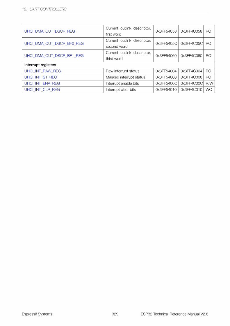
13. UART CONTROLLERS
UHCI_DMA_OUT_DSCR_REGCurrent outlink descriptor,
first word0x3FF54058 0x3FF4C058 RO
UHCI_DMA_OUT_DSCR_BF0_REGCurrent outlink descriptor,
second word0x3FF5405C 0x3FF4C05C RO
UHCI_DMA_OUT_DSCR_BF1_REGCurrent outlink descriptor,
third word0x3FF54060 0x3FF4C060 RO
Interrupt registers
UHCI_INT_RAW_REG Raw interrupt status 0x3FF54004 0x3FF4C004 RO
UHCI_INT_ST_REG Masked interrupt status 0x3FF54008 0x3FF4C008 RO
UHCI_INT_ENA_REG Interrupt enable bits 0x3FF5400C 0x3FF4C00C R/W
UHCI_INT_CLR_REG Interrupt clear bits 0x3FF54010 0x3FF4C010 WO
Espressif Systems 329 ESP32 Technical Reference Manual V2.8
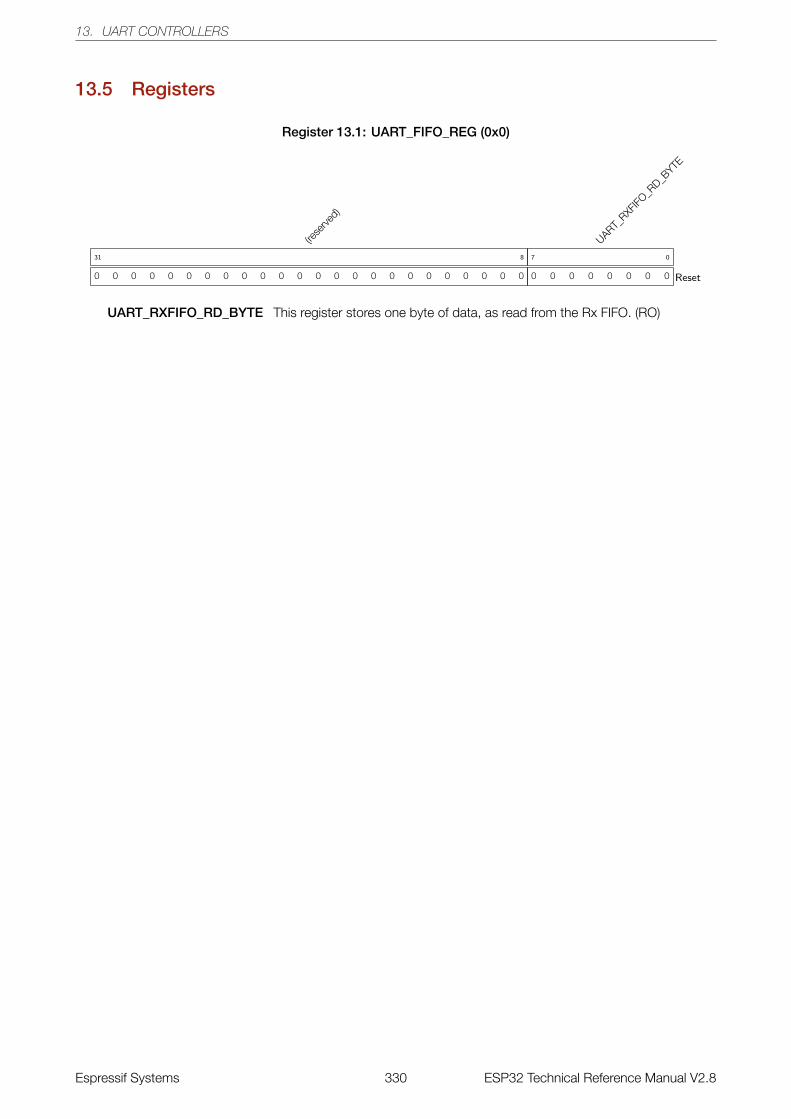
13. UART CONTROLLERS
13.5 Registers
Register 13.1: UART_FIFO_REG (0x0)
(rese
rved)
0 0 0 0 0 0 0 0 0 0 0 0 0 0 0 0 0 0 0 0 0 0 0 0
31 8
UART_RXF
IFO_R
D_BYTE
0 0 0 0 0 0 0 0
7 0
Reset
UART_RXFIFO_RD_BYTE This register stores one byte of data, as read from the Rx FIFO. (RO)
Espressif Systems 330 ESP32 Technical Reference Manual V2.8
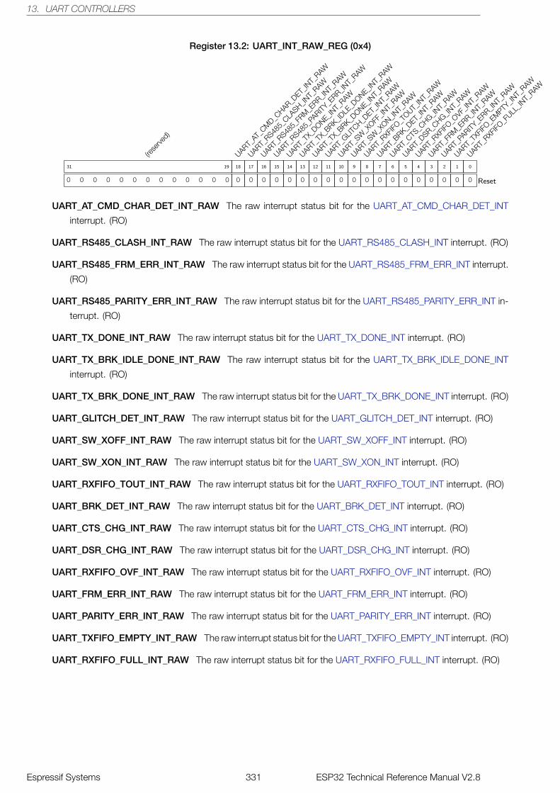
13. UART CONTROLLERS
Register 13.2: UART_INT_RAW_REG (0x4)
(rese
rved)
0 0 0 0 0 0 0 0 0 0 0 0 0
31 19
UART_AT
_CM
D_CHAR_D
ET_IN
T_RAW
0
18
UART_RS48
5_CLA
SH_INT_
RAW
0
17
UART_RS48
5_FR
M_E
RR_INT_
RAW
0
16
UART_RS48
5_PA
RITY_E
RR_INT_
RAW
0
15
UART_TX
_DONE_IN
T_RAW
0
14
UART_TX
_BRK_ID
LE_D
ONE_INT_
RAW
0
13
UART_TX
_BRK_D
ONE_INT_
RAW
0
12
UART_GLIT
CH_DET_
INT_
RAW
0
11
UART_SW
_XOFF
_INT_
RAW
0
10
UART_SW
_XON_IN
T_RAW
0
9
UART_RXF
IFO_T
OUT_IN
T_RAW
0
8
UART_BRK_D
ET_IN
T_RAW
0
7
UART_CTS
_CHG_IN
T_RAW
0
6
UART_DSR_C
HG_INT_
RAW
0
5
UART_RXF
IFO_O
VF_IN
T_RAW
0
4
UART_FR
M_E
RR_INT_
RAW
0
3
UART_PA
RITY_E
RR_INT_
RAW
0
2
UART_TX
FIFO_E
MPTY
_INT_
RAW
0
1
UART_RXF
IFO_F
ULL_IN
T_RAW
0
0
Reset
UART_AT_CMD_CHAR_DET_INT_RAW The raw interrupt status bit for the UART_AT_CMD_CHAR_DET_INT
interrupt. (RO)
UART_RS485_CLASH_INT_RAW The raw interrupt status bit for the UART_RS485_CLASH_INT interrupt. (RO)
UART_RS485_FRM_ERR_INT_RAW The raw interrupt status bit for the UART_RS485_FRM_ERR_INT interrupt.
(RO)
UART_RS485_PARITY_ERR_INT_RAW The raw interrupt status bit for the UART_RS485_PARITY_ERR_INT in-
terrupt. (RO)
UART_TX_DONE_INT_RAW The raw interrupt status bit for the UART_TX_DONE_INT interrupt. (RO)
UART_TX_BRK_IDLE_DONE_INT_RAW The raw interrupt status bit for the UART_TX_BRK_IDLE_DONE_INT
interrupt. (RO)
UART_TX_BRK_DONE_INT_RAW The raw interrupt status bit for the UART_TX_BRK_DONE_INT interrupt. (RO)
UART_GLITCH_DET_INT_RAW The raw interrupt status bit for the UART_GLITCH_DET_INT interrupt. (RO)
UART_SW_XOFF_INT_RAW The raw interrupt status bit for the UART_SW_XOFF_INT interrupt. (RO)
UART_SW_XON_INT_RAW The raw interrupt status bit for the UART_SW_XON_INT interrupt. (RO)
UART_RXFIFO_TOUT_INT_RAW The raw interrupt status bit for the UART_RXFIFO_TOUT_INT interrupt. (RO)
UART_BRK_DET_INT_RAW The raw interrupt status bit for the UART_BRK_DET_INT interrupt. (RO)
UART_CTS_CHG_INT_RAW The raw interrupt status bit for the UART_CTS_CHG_INT interrupt. (RO)
UART_DSR_CHG_INT_RAW The raw interrupt status bit for the UART_DSR_CHG_INT interrupt. (RO)
UART_RXFIFO_OVF_INT_RAW The raw interrupt status bit for the UART_RXFIFO_OVF_INT interrupt. (RO)
UART_FRM_ERR_INT_RAW The raw interrupt status bit for the UART_FRM_ERR_INT interrupt. (RO)
UART_PARITY_ERR_INT_RAW The raw interrupt status bit for the UART_PARITY_ERR_INT interrupt. (RO)
UART_TXFIFO_EMPTY_INT_RAW The raw interrupt status bit for the UART_TXFIFO_EMPTY_INT interrupt. (RO)
UART_RXFIFO_FULL_INT_RAW The raw interrupt status bit for the UART_RXFIFO_FULL_INT interrupt. (RO)
Espressif Systems 331 ESP32 Technical Reference Manual V2.8
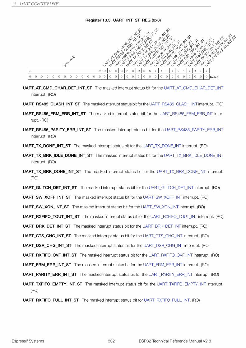
13. UART CONTROLLERS
Register 13.3: UART_INT_ST_REG (0x8)
(rese
rved)
0 0 0 0 0 0 0 0 0 0 0 0 0
31 19
UART_AT
_CM
D_CHAR_D
ET_IN
T_ST
0
18
UART_RS48
5_CLA
SH_INT_
ST
0
17
UART_RS48
5_FR
M_E
RR_INT_
ST
0
16
UART_RS48
5_PA
RITY_E
RR_INT_
ST
0
15
UART_TX
_DONE_IN
T_ST
0
14
UART_TX
_BRK_ID
LE_D
ONE_INT_
ST
0
13
UART_TX
_BRK_D
ONE_INT_
ST
0
12
UART_GLIT
CH_DET_
INT_
ST
0
11
UART_SW
_XOFF
_INT_
ST
0
10
UART_SW
_XON_IN
T_ST
0
9
UART_RXF
IFO_T
OUT_IN
T_ST
0
8
UART_BRK_D
ET_IN
T_ST
0
7
UART_CTS
_CHG_IN
T_ST
0
6
UART_DSR_C
HG_INT_
ST
0
5
UART_RXF
IFO_O
VF_IN
T_ST
0
4
UART_FR
M_E
RR_INT_
ST
0
3
UART_PA
RITY_E
RR_INT_
ST
0
2
UART_TX
FIFO_E
MPTY
_INT_
ST
0
1
UART_RXF
IFO_F
ULL_IN
T_ST
0
0
Reset
UART_AT_CMD_CHAR_DET_INT_ST The masked interrupt status bit for the UART_AT_CMD_CHAR_DET_INT
interrupt. (RO)
UART_RS485_CLASH_INT_ST The masked interrupt status bit for the UART_RS485_CLASH_INT interrupt. (RO)
UART_RS485_FRM_ERR_INT_ST The masked interrupt status bit for the UART_RS485_FRM_ERR_INT inter-
rupt. (RO)
UART_RS485_PARITY_ERR_INT_ST The masked interrupt status bit for the UART_RS485_PARITY_ERR_INT
interrupt. (RO)
UART_TX_DONE_INT_ST The masked interrupt status bit for the UART_TX_DONE_INT interrupt. (RO)
UART_TX_BRK_IDLE_DONE_INT_ST The masked interrupt status bit for the UART_TX_BRK_IDLE_DONE_INT
interrupt. (RO)
UART_TX_BRK_DONE_INT_ST The masked interrupt status bit for the UART_TX_BRK_DONE_INT interrupt.
(RO)
UART_GLITCH_DET_INT_ST The masked interrupt status bit for the UART_GLITCH_DET_INT interrupt. (RO)
UART_SW_XOFF_INT_ST The masked interrupt status bit for the UART_SW_XOFF_INT interrupt. (RO)
UART_SW_XON_INT_ST The masked interrupt status bit for the UART_SW_XON_INT interrupt. (RO)
UART_RXFIFO_TOUT_INT_ST The masked interrupt status bit for the UART_RXFIFO_TOUT_INT interrupt. (RO)
UART_BRK_DET_INT_ST The masked interrupt status bit for the UART_BRK_DET_INT interrupt. (RO)
UART_CTS_CHG_INT_ST The masked interrupt status bit for the UART_CTS_CHG_INT interrupt. (RO)
UART_DSR_CHG_INT_ST The masked interrupt status bit for the UART_DSR_CHG_INT interrupt. (RO)
UART_RXFIFO_OVF_INT_ST The masked interrupt status bit for the UART_RXFIFO_OVF_INT interrupt. (RO)
UART_FRM_ERR_INT_ST The masked interrupt status bit for the UART_FRM_ERR_INT interrupt. (RO)
UART_PARITY_ERR_INT_ST The masked interrupt status bit for the UART_PARITY_ERR_INT interrupt. (RO)
UART_TXFIFO_EMPTY_INT_ST The masked interrupt status bit for the UART_TXFIFO_EMPTY_INT interrupt.
(RO)
UART_RXFIFO_FULL_INT_ST The masked interrupt status bit for UART_RXFIFO_FULL_INT. (RO)
Espressif Systems 332 ESP32 Technical Reference Manual V2.8
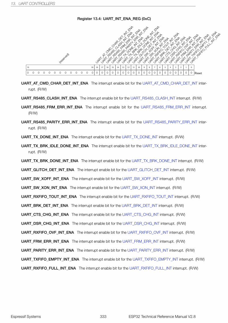
13. UART CONTROLLERS
Register 13.4: UART_INT_ENA_REG (0xC)
(rese
rved)
0 0 0 0 0 0 0 0 0 0 0 0 0
31 19
UART_AT
_CM
D_CHAR_D
ET_IN
T_ENA
0
18
UART_RS48
5_CLA
SH_INT_
ENA
0
17
UART_RS48
5_FR
M_E
RR_INT_
ENA
0
16
UART_RS48
5_PA
RITY_E
RR_INT_
ENA
0
15
UART_TX
_DONE_IN
T_ENA
0
14
UART_TX
_BRK_ID
LE_D
ONE_INT_
ENA
0
13
UART_TX
_BRK_D
ONE_INT_
ENA
0
12
UART_GLIT
CH_DET_
INT_
ENA
0
11
UART_SW
_XOFF
_INT_
ENA
0
10
UART_SW
_XON_IN
T_ENA
0
9
UART_RXF
IFO_T
OUT_IN
T_ENA
0
8
UART_BRK_D
ET_IN
T_ENA
0
7
UART_CTS
_CHG_IN
T_ENA
0
6
UART_DSR_C
HG_INT_
ENA
0
5
UART_RXF
IFO_O
VF_IN
T_ENA
0
4
UART_FR
M_E
RR_INT_
ENA
0
3
UART_PA
RITY_E
RR_INT_
ENA
0
2
UART_TX
FIFO_E
MPTY
_INT_
ENA
0
1
UART_RXF
IFO_F
ULL_IN
T_ENA
0
0
Reset
UART_AT_CMD_CHAR_DET_INT_ENA The interrupt enable bit for the UART_AT_CMD_CHAR_DET_INT inter-
rupt. (R/W)
UART_RS485_CLASH_INT_ENA The interrupt enable bit for the UART_RS485_CLASH_INT interrupt. (R/W)
UART_RS485_FRM_ERR_INT_ENA The interrupt enable bit for the UART_RS485_FRM_ERR_INT interrupt.
(R/W)
UART_RS485_PARITY_ERR_INT_ENA The interrupt enable bit for the UART_RS485_PARITY_ERR_INT inter-
rupt. (R/W)
UART_TX_DONE_INT_ENA The interrupt enable bit for the UART_TX_DONE_INT interrupt. (R/W)
UART_TX_BRK_IDLE_DONE_INT_ENA The interrupt enable bit for the UART_TX_BRK_IDLE_DONE_INT inter-
rupt. (R/W)
UART_TX_BRK_DONE_INT_ENA The interrupt enable bit for the UART_TX_BRK_DONE_INT interrupt. (R/W)
UART_GLITCH_DET_INT_ENA The interrupt enable bit for the UART_GLITCH_DET_INT interrupt. (R/W)
UART_SW_XOFF_INT_ENA The interrupt enable bit for the UART_SW_XOFF_INT interrupt. (R/W)
UART_SW_XON_INT_ENA The interrupt enable bit for the UART_SW_XON_INT interrupt. (R/W)
UART_RXFIFO_TOUT_INT_ENA The interrupt enable bit for the UART_RXFIFO_TOUT_INT interrupt. (R/W)
UART_BRK_DET_INT_ENA The interrupt enable bit for the UART_BRK_DET_INT interrupt. (R/W)
UART_CTS_CHG_INT_ENA The interrupt enable bit for the UART_CTS_CHG_INT interrupt. (R/W)
UART_DSR_CHG_INT_ENA The interrupt enable bit for the UART_DSR_CHG_INT interrupt. (R/W)
UART_RXFIFO_OVF_INT_ENA The interrupt enable bit for the UART_RXFIFO_OVF_INT interrupt. (R/W)
UART_FRM_ERR_INT_ENA The interrupt enable bit for the UART_FRM_ERR_INT interrupt. (R/W)
UART_PARITY_ERR_INT_ENA The interrupt enable bit for the UART_PARITY_ERR_INT interrupt. (R/W)
UART_TXFIFO_EMPTY_INT_ENA The interrupt enable bit for the UART_TXFIFO_EMPTY_INT interrupt. (R/W)
UART_RXFIFO_FULL_INT_ENA The interrupt enable bit for the UART_RXFIFO_FULL_INT interrupt. (R/W)
Espressif Systems 333 ESP32 Technical Reference Manual V2.8
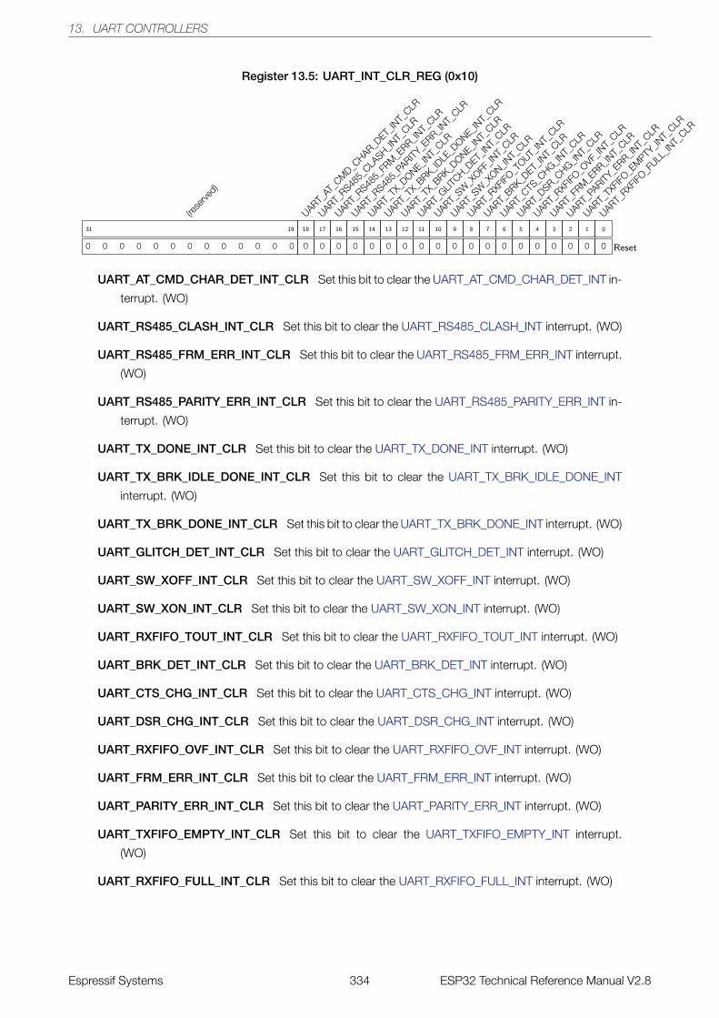
13. UART CONTROLLERS
Register 13.5: UART_INT_CLR_REG (0x10)
(rese
rved)
0 0 0 0 0 0 0 0 0 0 0 0 0
31 19
UART_AT
_CM
D_CHAR_D
ET_IN
T_CLR
0
18
UART_RS48
5_CLA
SH_INT_
CLR
0
17
UART_RS48
5_FR
M_E
RR_INT_
CLR
0
16
UART_RS48
5_PA
RITY_E
RR_INT_
CLR
0
15
UART_TX
_DONE_IN
T_CLR
0
14
UART_TX
_BRK_ID
LE_D
ONE_INT_
CLR
0
13
UART_TX
_BRK_D
ONE_INT_
CLR
0
12
UART_GLIT
CH_DET_
INT_
CLR
0
11
UART_SW
_XOFF
_INT_
CLR
0
10
UART_SW
_XON_IN
T_CLR
0
9
UART_RXF
IFO_T
OUT_IN
T_CLR
0
8
UART_BRK_D
ET_IN
T_CLR
0
7
UART_CTS
_CHG_IN
T_CLR
0
6
UART_DSR_C
HG_INT_
CLR
0
5
UART_RXF
IFO_O
VF_IN
T_CLR
0
4
UART_FR
M_E
RR_INT_
CLR
0
3
UART_PA
RITY_E
RR_INT_
CLR
0
2
UART_TX
FIFO_E
MPTY
_INT_
CLR
0
1
UART_RXF
IFO_F
ULL_IN
T_CLR
0
0
Reset
UART_AT_CMD_CHAR_DET_INT_CLR Set this bit to clear the UART_AT_CMD_CHAR_DET_INT in-
terrupt. (WO)
UART_RS485_CLASH_INT_CLR Set this bit to clear the UART_RS485_CLASH_INT interrupt. (WO)
UART_RS485_FRM_ERR_INT_CLR Set this bit to clear the UART_RS485_FRM_ERR_INT interrupt.
(WO)
UART_RS485_PARITY_ERR_INT_CLR Set this bit to clear the UART_RS485_PARITY_ERR_INT in-
terrupt. (WO)
UART_TX_DONE_INT_CLR Set this bit to clear the UART_TX_DONE_INT interrupt. (WO)
UART_TX_BRK_IDLE_DONE_INT_CLR Set this bit to clear the UART_TX_BRK_IDLE_DONE_INT
interrupt. (WO)
UART_TX_BRK_DONE_INT_CLR Set this bit to clear the UART_TX_BRK_DONE_INT interrupt. (WO)
UART_GLITCH_DET_INT_CLR Set this bit to clear the UART_GLITCH_DET_INT interrupt. (WO)
UART_SW_XOFF_INT_CLR Set this bit to clear the UART_SW_XOFF_INT interrupt. (WO)
UART_SW_XON_INT_CLR Set this bit to clear the UART_SW_XON_INT interrupt. (WO)
UART_RXFIFO_TOUT_INT_CLR Set this bit to clear the UART_RXFIFO_TOUT_INT interrupt. (WO)
UART_BRK_DET_INT_CLR Set this bit to clear the UART_BRK_DET_INT interrupt. (WO)
UART_CTS_CHG_INT_CLR Set this bit to clear the UART_CTS_CHG_INT interrupt. (WO)
UART_DSR_CHG_INT_CLR Set this bit to clear the UART_DSR_CHG_INT interrupt. (WO)
UART_RXFIFO_OVF_INT_CLR Set this bit to clear the UART_RXFIFO_OVF_INT interrupt. (WO)
UART_FRM_ERR_INT_CLR Set this bit to clear the UART_FRM_ERR_INT interrupt. (WO)
UART_PARITY_ERR_INT_CLR Set this bit to clear the UART_PARITY_ERR_INT interrupt. (WO)
UART_TXFIFO_EMPTY_INT_CLR Set this bit to clear the UART_TXFIFO_EMPTY_INT interrupt.
(WO)
UART_RXFIFO_FULL_INT_CLR Set this bit to clear the UART_RXFIFO_FULL_INT interrupt. (WO)
Espressif Systems 334 ESP32 Technical Reference Manual V2.8
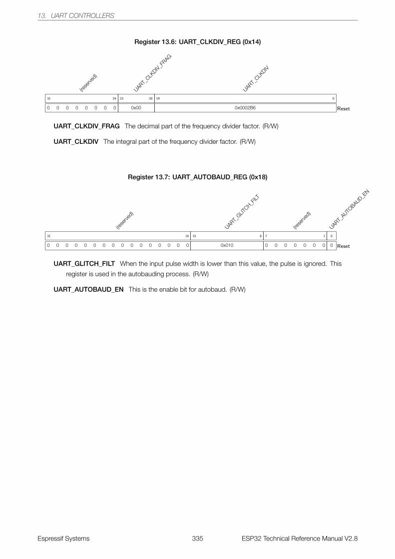
13. UART CONTROLLERS
Register 13.6: UART_CLKDIV_REG (0x14)
(rese
rved)
0 0 0 0 0 0 0 0
31 24
UART_CLK
DIV_FRAG
0x00
23 20
UART_CLK
DIV
0x0002B6
19 0
Reset
UART_CLKDIV_FRAG The decimal part of the frequency divider factor. (R/W)
UART_CLKDIV The integral part of the frequency divider factor. (R/W)
Register 13.7: UART_AUTOBAUD_REG (0x18)
(rese
rved)
0 0 0 0 0 0 0 0 0 0 0 0 0 0 0 0
31 16
UART_GLIT
CH_FILT
0x010
15 8
(rese
rved)
0 0 0 0 0 0 0
7 1
UART_AUTO
BAUD_EN
0
0
Reset
UART_GLITCH_FILT When the input pulse width is lower than this value, the pulse is ignored. This
register is used in the autobauding process. (R/W)
UART_AUTOBAUD_EN This is the enable bit for autobaud. (R/W)
Espressif Systems 335 ESP32 Technical Reference Manual V2.8
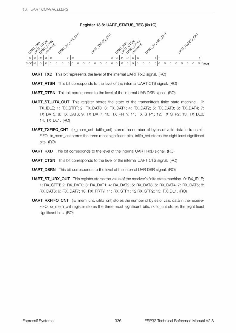
13. UART CONTROLLERS
Register 13.8: UART_STATUS_REG (0x1C)
UART_TX
D
0x000
31
UART_RTS
N
0
30
UART_DTR
N
0
29
(rese
rved)
0
28
UART_ST_
UTX_O
UT
0 0 0 0
27 24
UART_TX
FIFO_C
NT
0 0 0 0 0 0 0 0
23 16
UART_RXD
0
15
UART_CTS
N
0
14
UART_DSRN
0
13
(rese
rved)
0
12
UART_ST_
URX_OUT
0 0 0 0
11 8
UART_RXF
IFO_C
NT
0 0 0 0 0 0 0 0
7 0
Reset
UART_TXD This bit represents the level of the internal UART RxD signal. (RO)
UART_RTSN This bit corresponds to the level of the internal UART CTS signal. (RO)
UART_DTRN This bit corresponds to the level of the internal UAR DSR signal. (RO)
UART_ST_UTX_OUT This register stores the state of the transmitter’s finite state machine. 0:
TX_IDLE; 1: TX_STRT; 2: TX_DAT0; 3: TX_DAT1; 4: TX_DAT2; 5: TX_DAT3; 6: TX_DAT4; 7:
TX_DAT5; 8: TX_DAT6; 9: TX_DAT7; 10: TX_PRTY; 11: TX_STP1; 12: TX_STP2; 13: TX_DL0;
14: TX_DL1. (RO)
UART_TXFIFO_CNT (tx_mem_cnt, txfifo_cnt) stores the number of bytes of valid data in transmit-
FIFO. tx_mem_cnt stores the three most significant bits, txfifo_cnt stores the eight least significant
bits. (RO)
UART_RXD This bit corresponds to the level of the internal UART RxD signal. (RO)
UART_CTSN This bit corresponds to the level of the internal UART CTS signal. (RO)
UART_DSRN This bit corresponds to the level of the internal UAR DSR signal. (RO)
UART_ST_URX_OUT This register stores the value of the receiver’s finite state machine. 0: RX_IDLE;
1: RX_STRT; 2: RX_DAT0; 3: RX_DAT1; 4: RX_DAT2; 5: RX_DAT3; 6: RX_DAT4; 7: RX_DAT5; 8:
RX_DAT6; 9: RX_DAT7; 10: RX_PRTY; 11: RX_STP1; 12:RX_STP2; 13: RX_DL1. (RO)
UART_RXFIFO_CNT (rx_mem_cnt, rxfifo_cnt) stores the number of bytes of valid data in the receive-
FIFO. rx_mem_cnt register stores the three most significant bits, rxfifo_cnt stores the eight least
significant bits. (RO)
Espressif Systems 336 ESP32 Technical Reference Manual V2.8
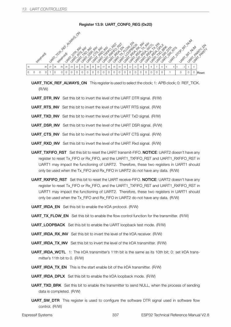
13. UART CONTROLLERS
Register 13.9: UART_CONF0_REG (0x20)
(rese
rved)
0 0 0 0
31 28
UART_TIC
K_REF_
ALWAY
S_ON
1
27
(rese
rved)
0 0
26 25
UART_DTR
_INV
0
24
UART_RTS
_INV
0
23
UART_TX
D_INV
0
22
UART_DSR_IN
V
0
21
UART_CTS
_INV
0
20
UART_RXD
_INV
0
19
UART_TX
FIFO_R
ST
0
18
UART_RXF
IFO_R
ST
0
17
UART_IR
DA_EN
0
16
UART_TX
_FLO
W_E
N
0
15
UART_LO
OPBACK
0
14
UART_IR
DA_RX_
INV
0
13
UART_IR
DA_TX_
INV
0
12
UART_IR
DA_WCTL
0
11
UART_IR
DA_TX_
EN
0
10
UART_IR
DA_DPLX
0
9
UART_TX
D_BRK
0
8
UART_SW
_DTR
0
7
UART_SW
_RTS
0
6
UART_STO
P_BIT_
NUM
1
5 4
UART_BIT_
NUM
3
3 2
UART_PA
RITY_E
N
0
1
UART_PA
RITY
0
0
Reset
UART_TICK_REF_ALWAYS_ON This register is used to select the clock; 1: APB clock; 0: REF_TICK.
(R/W)
UART_DTR_INV Set this bit to invert the level of the UART DTR signal. (R/W)
UART_RTS_INV Set this bit to invert the level of the UART RTS signal. (R/W)
UART_TXD_INV Set this bit to invert the level of the UART TxD signal. (R/W)
UART_DSR_INV Set this bit to invert the level of the UART DSR signal. (R/W)
UART_CTS_INV Set this bit to invert the level of the UART CTS signal. (R/W)
UART_RXD_INV Set this bit to invert the level of the UART Rxd signal. (R/W)
UART_TXFIFO_RST Set this bit to reset the UART transmit-FIFO. NOTICE: UART2 doesn’t have any
register to reset Tx_FIFO or Rx_FIFO, and the UART1_TXFIFO_RST and UART1_RXFIFO_RST in
UART1 may impact the functioning of UART2. Therefore, these two registers in UART1 should
only be used when the Tx_FIFO and Rx_FIFO in UART2 do not have any data. (R/W)
UART_RXFIFO_RST Set this bit to reset the UART receive-FIFO. NOTICE: UART2 doesn’t have any
register to reset Tx_FIFO or Rx_FIFO, and the UART1_TXFIFO_RST and UART1_RXFIFO_RST in
UART1 may impact the functioning of UART2. Therefore, these two registers in UART1 should
only be used when the Tx_FIFO and Rx_FIFO in UART2 do not have any data. (R/W)
UART_IRDA_EN Set this bit to enable the IrDA protocol. (R/W)
UART_TX_FLOW_EN Set this bit to enable the flow control function for the transmitter. (R/W)
UART_LOOPBACK Set this bit to enable the UART loopback test mode. (R/W)
UART_IRDA_RX_INV Set this bit to invert the level of the IrDA receiver. (R/W)
UART_IRDA_TX_INV Set this bit to invert the level of the IrDA transmitter. (R/W)
UART_IRDA_WCTL 1: The IrDA transmitter’s 11th bit is the same as its 10th bit; 0: set IrDA trans-
mitter’s 11th bit to 0. (R/W)
UART_IRDA_TX_EN This is the start enable bit of the IrDA transmitter. (R/W)
UART_IRDA_DPLX Set this bit to enable the IrDA loopback mode. (R/W)
UART_TXD_BRK Set this bit to enable the transmitter to send NULL, when the process of sending
data is completed. (R/W)
UART_SW_DTR This register is used to configure the software DTR signal used in software flow
control. (R/W)
Espressif Systems 337 ESP32 Technical Reference Manual V2.8
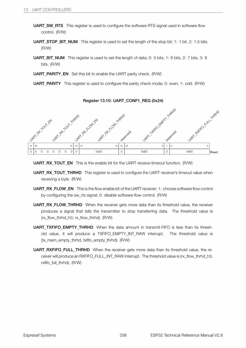
13. UART CONTROLLERS
UART_SW_RTS This register is used to configure the software RTS signal used in software flow
control. (R/W)
UART_STOP_BIT_NUM This register is used to set the length of the stop bit; 1: 1 bit, 2: 1.5 bits.
(R/W)
UART_BIT_NUM This register is used to set the length of data; 0: 5 bits, 1: 6 bits, 2: 7 bits, 3: 8
bits. (R/W)
UART_PARITY_EN Set this bit to enable the UART parity check. (R/W)
UART_PARITY This register is used to configure the parity check mode; 0: even, 1: odd. (R/W)
Register 13.10: UART_CONF1_REG (0x24)
UART_RX_
TOUT_
EN
0
31
UART_RX_
TOUT_
THRHD
0 0 0 0 0 0 0
30 24
UART_RX_
FLOW
_EN
0
23
UART_RX_
FLOW
_THRHD
0x00
22 16
(rese
rved)
0
15
UART_TX
FIFO_E
MPTY
_THRHD
0x60
14 8
(rese
rved)
0
7
UART_RXF
IFO_F
ULL_T
HRHD
0x60
6 0
Reset
UART_RX_TOUT_EN This is the enable bit for the UART receive-timeout function. (R/W)
UART_RX_TOUT_THRHD This register is used to configure the UART receiver’s timeout value when
receiving a byte. (R/W)
UART_RX_FLOW_EN This is the flow enable bit of the UART receiver; 1: choose software flow control
by configuring the sw_rts signal; 0: disable software flow control. (R/W)
UART_RX_FLOW_THRHD When the receiver gets more data than its threshold value, the receiver
produces a signal that tells the transmitter to stop transferring data. The threshold value is
(rx_flow_thrhd_h3, rx_flow_thrhd). (R/W)
UART_TXFIFO_EMPTY_THRHD When the data amount in transmit-FIFO is less than its thresh-
old value, it will produce a TXFIFO_EMPTY_INT_RAW interrupt. The threshold value is
(tx_mem_empty_thrhd, txfifo_empty_thrhd). (R/W)
UART_RXFIFO_FULL_THRHD When the receiver gets more data than its threshold value, the re-
ceiver will produce an RXFIFO_FULL_INT_RAW interrupt. The threshold value is (rx_flow_thrhd_h3,
rxfifo_full_thrhd). (R/W)
Espressif Systems 338 ESP32 Technical Reference Manual V2.8
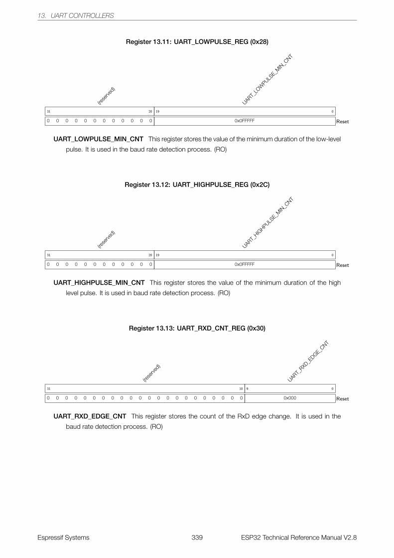
13. UART CONTROLLERS
Register 13.11: UART_LOWPULSE_REG (0x28)
(rese
rved)
0 0 0 0 0 0 0 0 0 0 0 0
31 20
UART_LO
WPULS
E_MIN
_CNT
0x0FFFFF
19 0
Reset
UART_LOWPULSE_MIN_CNT This register stores the value of the minimum duration of the low-level
pulse. It is used in the baud rate detection process. (RO)
Register 13.12: UART_HIGHPULSE_REG (0x2C)
(rese
rved)
0 0 0 0 0 0 0 0 0 0 0 0
31 20
UART_HIG
HPULSE_M
IN_C
NT
0x0FFFFF
19 0
Reset
UART_HIGHPULSE_MIN_CNT This register stores the value of the minimum duration of the high
level pulse. It is used in baud rate detection process. (RO)
Register 13.13: UART_RXD_CNT_REG (0x30)
(rese
rved)
0 0 0 0 0 0 0 0 0 0 0 0 0 0 0 0 0 0 0 0 0 0
31 10
UART_RXD
_EDGE_C
NT
0x000
9 0
Reset
UART_RXD_EDGE_CNT This register stores the count of the RxD edge change. It is used in the
baud rate detection process. (RO)
Espressif Systems 339 ESP32 Technical Reference Manual V2.8
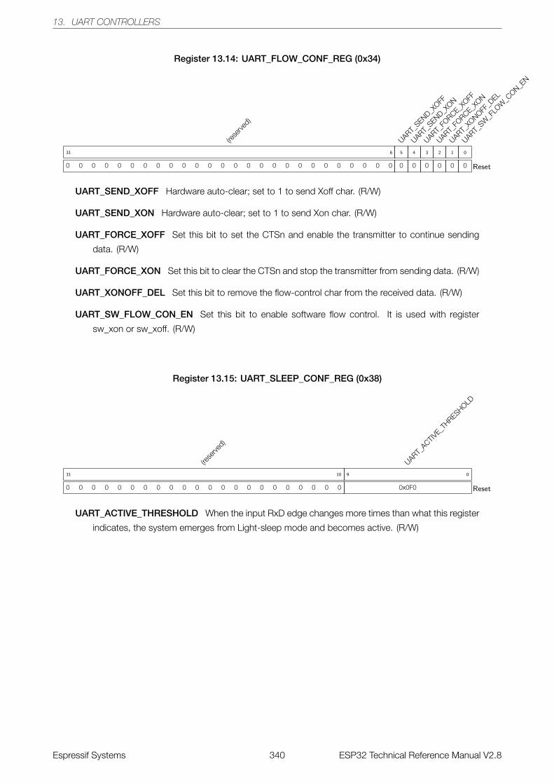
13. UART CONTROLLERS
Register 13.14: UART_FLOW_CONF_REG (0x34)
(rese
rved)
0 0 0 0 0 0 0 0 0 0 0 0 0 0 0 0 0 0 0 0 0 0 0 0 0 0
31 6
UART_SEND_X
OFF
0
5
UART_SEND_X
ON
0
4
UART_FO
RCE_XOFF
0
3
UART_FO
RCE_XON
0
2
UART_XO
NOFF_D
EL
0
1
UART_SW
_FLO
W_C
ON_EN
0
0
Reset
UART_SEND_XOFF Hardware auto-clear; set to 1 to send Xoff char. (R/W)
UART_SEND_XON Hardware auto-clear; set to 1 to send Xon char. (R/W)
UART_FORCE_XOFF Set this bit to set the CTSn and enable the transmitter to continue sending
data. (R/W)
UART_FORCE_XON Set this bit to clear the CTSn and stop the transmitter from sending data. (R/W)
UART_XONOFF_DEL Set this bit to remove the flow-control char from the received data. (R/W)
UART_SW_FLOW_CON_EN Set this bit to enable software flow control. It is used with register
sw_xon or sw_xoff. (R/W)
Register 13.15: UART_SLEEP_CONF_REG (0x38)
(rese
rved)
0 0 0 0 0 0 0 0 0 0 0 0 0 0 0 0 0 0 0 0 0 0
31 10
UART_ACTIV
E_THRESHOLD
0x0F0
9 0
Reset
UART_ACTIVE_THRESHOLD When the input RxD edge changes more times than what this register
indicates, the system emerges from Light-sleep mode and becomes active. (R/W)
Espressif Systems 340 ESP32 Technical Reference Manual V2.8
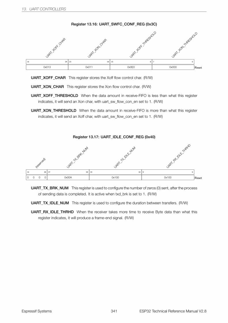
13. UART CONTROLLERS
Register 13.16: UART_SWFC_CONF_REG (0x3C)
UART_XO
FF_C
HAR
0x013
31 24
UART_XO
N_CHAR
0x011
23 16
UART_XO
FF_T
HRESHOLD
0x0E0
15 8
UART_XO
N_THRESHOLD
0x000
7 0
Reset
UART_XOFF_CHAR This register stores the Xoff flow control char. (R/W)
UART_XON_CHAR This register stores the Xon flow control char. (R/W)
UART_XOFF_THRESHOLD When the data amount in receive-FIFO is less than what this register
indicates, it will send an Xon char, with uart_sw_flow_con_en set to 1. (R/W)
UART_XON_THRESHOLD When the data amount in receive-FIFO is more than what this register
indicates, it will send an Xoff char, with uart_sw_flow_con_en set to 1. (R/W)
Register 13.17: UART_IDLE_CONF_REG (0x40)
(rese
rved)
0 0 0 0
31 28
UART_TX
_BRK_N
UM
0x00A
27 20
UART_TX
_IDLE
_NUM
0x100
19 10
UART_RX_
IDLE
_THRHD
0x100
9 0
Reset
UART_TX_BRK_NUM This register is used to configure the number of zeros (0) sent, after the process
of sending data is completed. It is active when txd_brk is set to 1. (R/W)
UART_TX_IDLE_NUM This register is used to configure the duration between transfers. (R/W)
UART_RX_IDLE_THRHD When the receiver takes more time to receive Byte data than what this
register indicates, it will produce a frame-end signal. (R/W)
Espressif Systems 341 ESP32 Technical Reference Manual V2.8
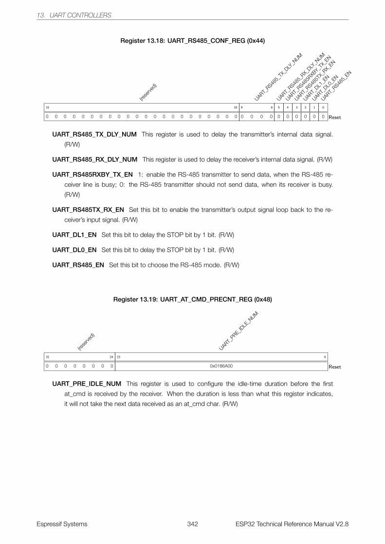
13. UART CONTROLLERS
Register 13.18: UART_RS485_CONF_REG (0x44)
(rese
rved)
0 0 0 0 0 0 0 0 0 0 0 0 0 0 0 0 0 0 0 0 0 0
31 10
UART_RS48
5_TX
_DLY
_NUM
0 0 0 0
9 6
UART_RS48
5_RX_
DLY_N
UM
0
5
UART_RS48
5RXB
Y_TX_
EN
0
4
UART_RS48
5TX_
RX_EN
0
3
UART_DL1
_EN
0
2
UART_DL0
_EN
0
1
UART_RS48
5_EN
0
0
Reset
UART_RS485_TX_DLY_NUM This register is used to delay the transmitter’s internal data signal.
(R/W)
UART_RS485_RX_DLY_NUM This register is used to delay the receiver’s internal data signal. (R/W)
UART_RS485RXBY_TX_EN 1: enable the RS-485 transmitter to send data, when the RS-485 re-
ceiver line is busy; 0: the RS-485 transmitter should not send data, when its receiver is busy.
(R/W)
UART_RS485TX_RX_EN Set this bit to enable the transmitter’s output signal loop back to the re-
ceiver’s input signal. (R/W)
UART_DL1_EN Set this bit to delay the STOP bit by 1 bit. (R/W)
UART_DL0_EN Set this bit to delay the STOP bit by 1 bit. (R/W)
UART_RS485_EN Set this bit to choose the RS-485 mode. (R/W)
Register 13.19: UART_AT_CMD_PRECNT_REG (0x48)
(rese
rved)
0 0 0 0 0 0 0 0
31 24
UART_PRE_ID
LE_N
UM
0x0186A00
23 0
Reset
UART_PRE_IDLE_NUM This register is used to configure the idle-time duration before the first
at_cmd is received by the receiver. When the duration is less than what this register indicates,
it will not take the next data received as an at_cmd char. (R/W)
Espressif Systems 342 ESP32 Technical Reference Manual V2.8
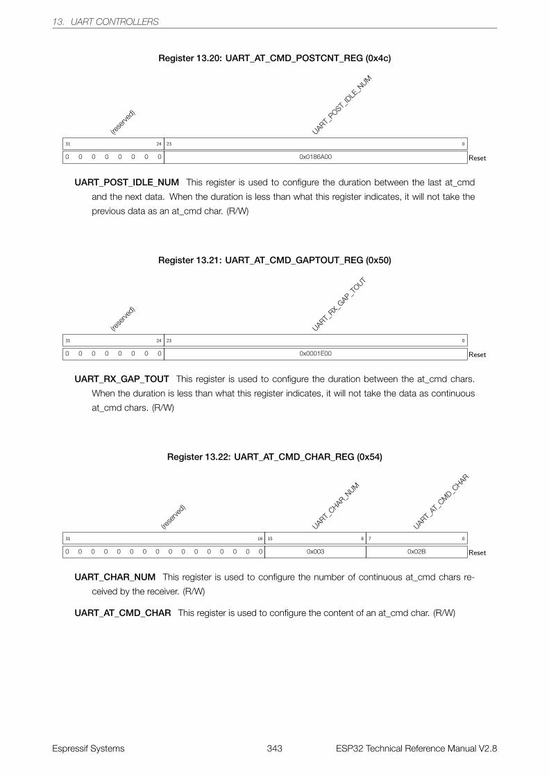
13. UART CONTROLLERS
Register 13.20: UART_AT_CMD_POSTCNT_REG (0x4c)
(rese
rved)
0 0 0 0 0 0 0 0
31 24
UART_POST_
IDLE
_NUM
0x0186A00
23 0
Reset
UART_POST_IDLE_NUM This register is used to configure the duration between the last at_cmd
and the next data. When the duration is less than what this register indicates, it will not take the
previous data as an at_cmd char. (R/W)
Register 13.21: UART_AT_CMD_GAPTOUT_REG (0x50)
(rese
rved)
0 0 0 0 0 0 0 0
31 24
UART_RX_
GAP_TOUT
0x0001E00
23 0
Reset
UART_RX_GAP_TOUT This register is used to configure the duration between the at_cmd chars.
When the duration is less than what this register indicates, it will not take the data as continuous
at_cmd chars. (R/W)
Register 13.22: UART_AT_CMD_CHAR_REG (0x54)
(rese
rved)
0 0 0 0 0 0 0 0 0 0 0 0 0 0 0 0
31 16
UART_CHAR_N
UM
0x003
15 8
UART_AT
_CM
D_CHAR
0x02B
7 0
Reset
UART_CHAR_NUM This register is used to configure the number of continuous at_cmd chars re-
ceived by the receiver. (R/W)
UART_AT_CMD_CHAR This register is used to configure the content of an at_cmd char. (R/W)
Espressif Systems 343 ESP32 Technical Reference Manual V2.8
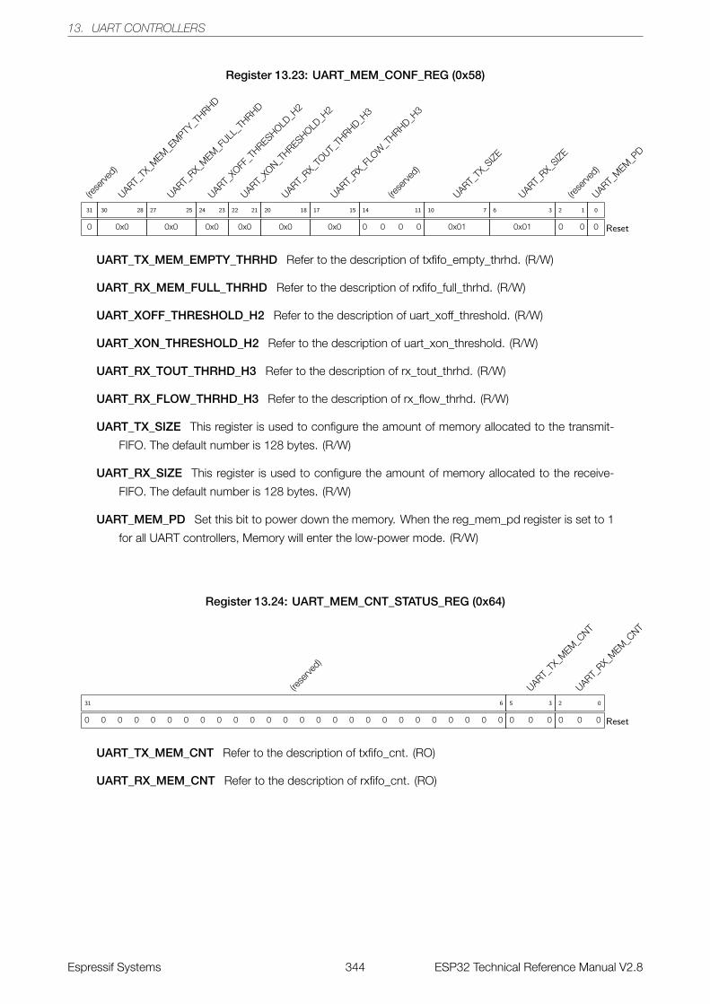
13. UART CONTROLLERS
Register 13.23: UART_MEM_CONF_REG (0x58)
(rese
rved)
0
31
UART_TX
_MEM
_EM
PTY_T
HRHD
0x0
30 28
UART_RX_
MEM
_FULL
_THRHD
0x0
27 25
UART_XO
FF_T
HRESHOLD_H
2
0x0
24 23
UART_XO
N_THRESHOLD
_H2
0x0
22 21
UART_RX_
TOUT_
THRHD_H
3
0x0
20 18
UART_RX_
FLOW
_THRHD_H
3
0x0
17 15
(rese
rved)
0 0 0 0
14 11
UART_TX
_SIZE
0x01
10 7
UART_RX_
SIZE
0x01
6 3
(rese
rved)
0 0
2 1
UART_M
EM_P
D
0
0
Reset
UART_TX_MEM_EMPTY_THRHD Refer to the description of txfifo_empty_thrhd. (R/W)
UART_RX_MEM_FULL_THRHD Refer to the description of rxfifo_full_thrhd. (R/W)
UART_XOFF_THRESHOLD_H2 Refer to the description of uart_xoff_threshold. (R/W)
UART_XON_THRESHOLD_H2 Refer to the description of uart_xon_threshold. (R/W)
UART_RX_TOUT_THRHD_H3 Refer to the description of rx_tout_thrhd. (R/W)
UART_RX_FLOW_THRHD_H3 Refer to the description of rx_flow_thrhd. (R/W)
UART_TX_SIZE This register is used to configure the amount of memory allocated to the transmit-
FIFO. The default number is 128 bytes. (R/W)
UART_RX_SIZE This register is used to configure the amount of memory allocated to the receive-
FIFO. The default number is 128 bytes. (R/W)
UART_MEM_PD Set this bit to power down the memory. When the reg_mem_pd register is set to 1
for all UART controllers, Memory will enter the low-power mode. (R/W)
Register 13.24: UART_MEM_CNT_STATUS_REG (0x64)
(rese
rved)
0 0 0 0 0 0 0 0 0 0 0 0 0 0 0 0 0 0 0 0 0 0 0 0 0 0
31 6
UART_TX
_MEM
_CNT
0 0 0
5 3
UART_RX_
MEM
_CNT
0 0 0
2 0
Reset
UART_TX_MEM_CNT Refer to the description of txfifo_cnt. (RO)
UART_RX_MEM_CNT Refer to the description of rxfifo_cnt. (RO)
Espressif Systems 344 ESP32 Technical Reference Manual V2.8
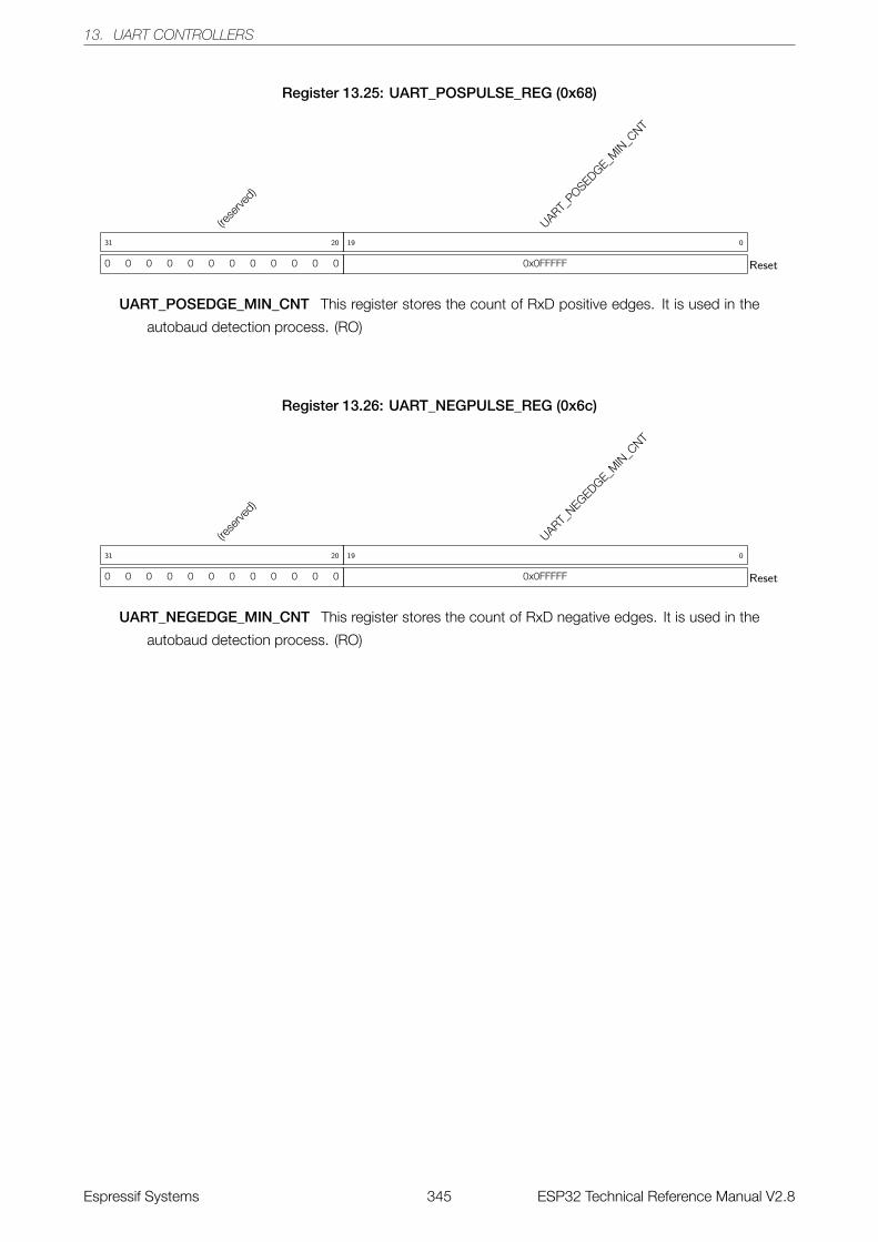
13. UART CONTROLLERS
Register 13.25: UART_POSPULSE_REG (0x68)
(rese
rved)
0 0 0 0 0 0 0 0 0 0 0 0
31 20
UART_POSEDGE_M
IN_C
NT
0x0FFFFF
19 0
Reset
UART_POSEDGE_MIN_CNT This register stores the count of RxD positive edges. It is used in the
autobaud detection process. (RO)
Register 13.26: UART_NEGPULSE_REG (0x6c)
(rese
rved)
0 0 0 0 0 0 0 0 0 0 0 0
31 20
UART_NEGEDGE_M
IN_C
NT
0x0FFFFF
19 0
Reset
UART_NEGEDGE_MIN_CNT This register stores the count of RxD negative edges. It is used in the
autobaud detection process. (RO)
Espressif Systems 345 ESP32 Technical Reference Manual V2.8

13. UART CONTROLLERS
Register 13.27: UHCI_CONF0_REG (0x0)
(rese
rved)
0 0 0 0 0 0 0 0 0 0
31 22
UHCI_ENCODE_C
RC_EN
1
21
UHCI_LEN_E
OF_EN
1
20
UHCI_UART_
IDLE
_EOF_
EN
0
19
UHCI_CRC_R
EC_EN
1
18
UHCI_HEAD_E
N
1
17
UHCI_SEPER_E
N
1
16
(rese
rved)
0 0 0 0
15 12
UHCI_UART2
_CE
0
11
UHCI_UART1
_CE
0
10
UHCI_UART0
_CE
0
9
(rese
rved)
0 0 0 0 0 0 0 0 0
17 9
Reset
UHCI_ENCODE_CRC_EN Reserved. Please initialize it to 0. (R/W)
UHCI_LEN_EOF_EN Reserved. Please initialize it to 0. (R/W)
UHCI_UART_IDLE_EOF_EN Reserved. Please initialize it to 0. (R/W)
UHCI_CRC_REC_EN Reserved. Please initialize it to 0. (R/W)
UHCI_HEAD_EN Reserved. Please initialize it to 0. (R/W)
UHCI_SEPER_EN Set this bit to use a special char and separate the data frame. (R/W)
UHCI_UART2_CE Set this bit to use UART2 and transmit or receive data. (R/W)
UHCI_UART1_CE Set this bit to use UART1 and transmit or receive data. (R/W)
UHCI_UART0_CE Set this bit to use UART and transmit or receive data. (R/W)
Espressif Systems 346 ESP32 Technical Reference Manual V2.8
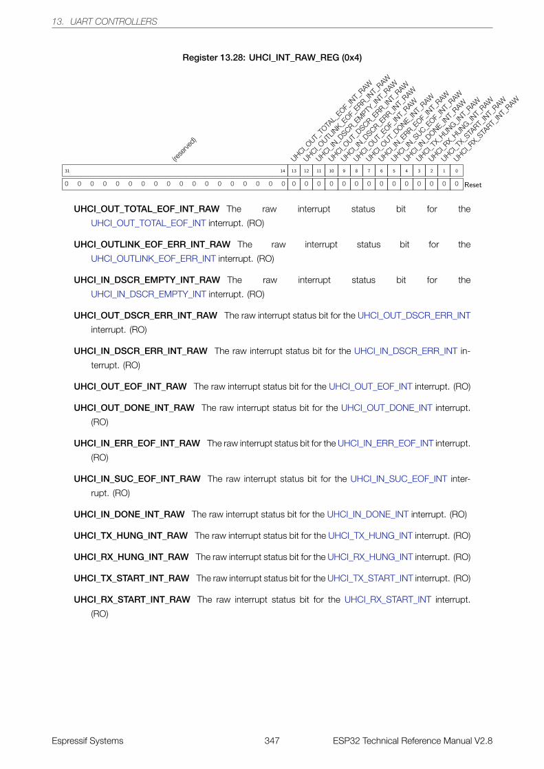
13. UART CONTROLLERS
Register 13.28: UHCI_INT_RAW_REG (0x4)
(rese
rved)
0 0 0 0 0 0 0 0 0 0 0 0 0 0 0 0 0 0
31 14
UHCI_OUT_
TOTA
L_EOF_
INT_
RAW
0
13
UHCI_OUTL
INK_E
OF_ERR_IN
T_RAW
0
12
UHCI_IN_D
SCR_EM
PTY_IN
T_RAW
0
11
UHCI_OUT_
DSCR_ERR_IN
T_RAW
0
10
UHCI_IN_D
SCR_ERR_IN
T_RAW
0
9
UHCI_OUT_
EOF_IN
T_RAW
0
8
UHCI_OUT_
DONE_INT_
RAW
0
7
UHCI_IN_E
RR_EOF_
INT_
RAW
0
6
UHCI_IN_S
UC_EOF_
INT_
RAW
0
5
UHCI_IN_D
ONE_INT_
RAW
0
4
UHCI_TX_
HUNG_INT_
RAW
0
3
UHCI_RX_
HUNG_INT_
RAW
0
2
UHCI_TX_
START_
INT_
RAW
0
1
UHCI_RX_
START_
INT_
RAW
0
0
Reset
UHCI_OUT_TOTAL_EOF_INT_RAW The raw interrupt status bit for the
UHCI_OUT_TOTAL_EOF_INT interrupt. (RO)
UHCI_OUTLINK_EOF_ERR_INT_RAW The raw interrupt status bit for the
UHCI_OUTLINK_EOF_ERR_INT interrupt. (RO)
UHCI_IN_DSCR_EMPTY_INT_RAW The raw interrupt status bit for the
UHCI_IN_DSCR_EMPTY_INT interrupt. (RO)
UHCI_OUT_DSCR_ERR_INT_RAW The raw interrupt status bit for the UHCI_OUT_DSCR_ERR_INT
interrupt. (RO)
UHCI_IN_DSCR_ERR_INT_RAW The raw interrupt status bit for the UHCI_IN_DSCR_ERR_INT in-
terrupt. (RO)
UHCI_OUT_EOF_INT_RAW The raw interrupt status bit for the UHCI_OUT_EOF_INT interrupt. (RO)
UHCI_OUT_DONE_INT_RAW The raw interrupt status bit for the UHCI_OUT_DONE_INT interrupt.
(RO)
UHCI_IN_ERR_EOF_INT_RAW The raw interrupt status bit for the UHCI_IN_ERR_EOF_INT interrupt.
(RO)
UHCI_IN_SUC_EOF_INT_RAW The raw interrupt status bit for the UHCI_IN_SUC_EOF_INT inter-
rupt. (RO)
UHCI_IN_DONE_INT_RAW The raw interrupt status bit for the UHCI_IN_DONE_INT interrupt. (RO)
UHCI_TX_HUNG_INT_RAW The raw interrupt status bit for the UHCI_TX_HUNG_INT interrupt. (RO)
UHCI_RX_HUNG_INT_RAW The raw interrupt status bit for the UHCI_RX_HUNG_INT interrupt. (RO)
UHCI_TX_START_INT_RAW The raw interrupt status bit for the UHCI_TX_START_INT interrupt. (RO)
UHCI_RX_START_INT_RAW The raw interrupt status bit for the UHCI_RX_START_INT interrupt.
(RO)
Espressif Systems 347 ESP32 Technical Reference Manual V2.8
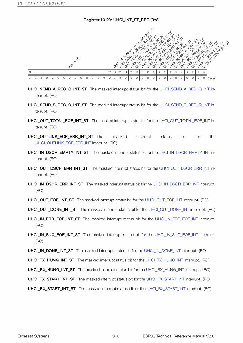
13. UART CONTROLLERS
Register 13.29: UHCI_INT_ST_REG (0x8)
(rese
rved)
0 0 0 0 0 0 0 0 0 0 0 0 0 0 0
31 17
UHCI_DM
A_INFIF
O_FULL
_WM
_INT_
ST
0
16
UHCI_SEND_A
_REG_Q
_INT_
ST
0
15
UHCI_SEND_S
_REG_Q
_INT_
ST
0
14
UHCI_OUT_
TOTA
L_EOF_
INT_
ST
0
13
UHCI_OUTL
INK_E
OF_ERR_IN
T_ST
0
12
UHCI_IN_D
SCR_EM
PTY_IN
T_ST
0
11
UHCI_OUT_
DSCR_ERR_IN
T_ST
0
10
UHCI_IN_D
SCR_ERR_IN
T_ST
0
9
UHCI_OUT_
EOF_IN
T_ST
0
8
UHCI_OUT_
DONE_INT_
ST
0
7
UHCI_IN_E
RR_EOF_
INT_
ST
0
6
UHCI_IN_S
UC_EOF_
INT_
ST
0
5
UHCI_IN_D
ONE_INT_
ST
0
4
UHCI_TX_
HUNG_INT_
ST
0
3
UHCI_RX_
HUNG_INT_
ST
0
2
UHCI_TX_
START_
INT_
ST
0
1
UHCI_RX_
START_
INT_
ST
0
0
Reset
UHCI_SEND_A_REG_Q_INT_ST The masked interrupt status bit for the UHCI_SEND_A_REG_Q_INT in-
terrupt. (RO)
UHCI_SEND_S_REG_Q_INT_ST The masked interrupt status bit for the UHCI_SEND_S_REG_Q_INT in-
terrupt. (RO)
UHCI_OUT_TOTAL_EOF_INT_ST The masked interrupt status bit for the UHCI_OUT_TOTAL_EOF_INT in-
terrupt. (RO)
UHCI_OUTLINK_EOF_ERR_INT_ST The masked interrupt status bit for the
UHCI_OUTLINK_EOF_ERR_INT interrupt. (RO)
UHCI_IN_DSCR_EMPTY_INT_ST The masked interrupt status bit for the UHCI_IN_DSCR_EMPTY_INT in-
terrupt. (RO)
UHCI_OUT_DSCR_ERR_INT_ST The masked interrupt status bit for the UHCI_OUT_DSCR_ERR_INT in-
terrupt. (RO)
UHCI_IN_DSCR_ERR_INT_ST The masked interrupt status bit for the UHCI_IN_DSCR_ERR_INT interrupt.
(RO)
UHCI_OUT_EOF_INT_ST The masked interrupt status bit for the UHCI_OUT_EOF_INT interrupt. (RO)
UHCI_OUT_DONE_INT_ST The masked interrupt status bit for the UHCI_OUT_DONE_INT interrupt. (RO)
UHCI_IN_ERR_EOF_INT_ST The masked interrupt status bit for the UHCI_IN_ERR_EOF_INT interrupt.
(RO)
UHCI_IN_SUC_EOF_INT_ST The masked interrupt status bit for the UHCI_IN_SUC_EOF_INT interrupt.
(RO)
UHCI_IN_DONE_INT_ST The masked interrupt status bit for the UHCI_IN_DONE_INT interrupt. (RO)
UHCI_TX_HUNG_INT_ST The masked interrupt status bit for the UHCI_TX_HUNG_INT interrupt. (RO)
UHCI_RX_HUNG_INT_ST The masked interrupt status bit for the UHCI_RX_HUNG_INT interrupt. (RO)
UHCI_TX_START_INT_ST The masked interrupt status bit for the UHCI_TX_START_INT interrupt. (RO)
UHCI_RX_START_INT_ST The masked interrupt status bit for the UHCI_RX_START_INT interrupt. (RO)
Espressif Systems 348 ESP32 Technical Reference Manual V2.8
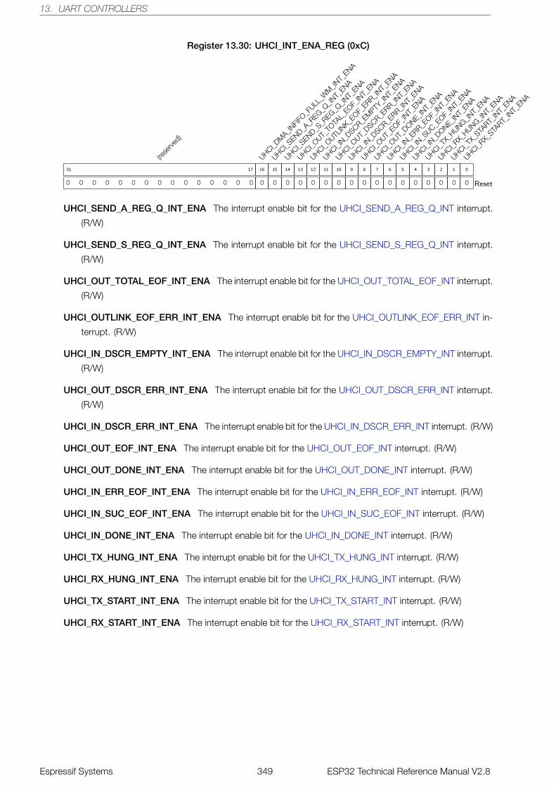
13. UART CONTROLLERS
Register 13.30: UHCI_INT_ENA_REG (0xC)
(rese
rved)
0 0 0 0 0 0 0 0 0 0 0 0 0 0 0
31 17
UHCI_DM
A_INFIF
O_FULL
_WM
_INT_
ENA
0
16
UHCI_SEND_A
_REG_Q
_INT_
ENA
0
15
UHCI_SEND_S
_REG_Q
_INT_
ENA
0
14
UHCI_OUT_
TOTA
L_EOF_
INT_
ENA
0
13
UHCI_OUTL
INK_E
OF_ERR_IN
T_ENA
0
12
UHCI_IN_D
SCR_EM
PTY_IN
T_ENA
0
11
UHCI_OUT_
DSCR_ERR_IN
T_ENA
0
10
UHCI_IN_D
SCR_ERR_IN
T_ENA
0
9
UHCI_OUT_
EOF_IN
T_ENA
0
8
UHCI_OUT_
DONE_INT_
ENA
0
7
UHCI_IN_E
RR_EOF_
INT_
ENA
0
6
UHCI_IN_S
UC_EOF_
INT_
ENA
0
5
UHCI_IN_D
ONE_INT_
ENA
0
4
UHCI_TX_
HUNG_INT_
ENA
0
3
UHCI_RX_
HUNG_INT_
ENA
0
2
UHCI_TX_
START_
INT_
ENA
0
1
UHCI_RX_
START_
INT_
ENA
0
0
Reset
UHCI_SEND_A_REG_Q_INT_ENA The interrupt enable bit for the UHCI_SEND_A_REG_Q_INT interrupt.
(R/W)
UHCI_SEND_S_REG_Q_INT_ENA The interrupt enable bit for the UHCI_SEND_S_REG_Q_INT interrupt.
(R/W)
UHCI_OUT_TOTAL_EOF_INT_ENA The interrupt enable bit for the UHCI_OUT_TOTAL_EOF_INT interrupt.
(R/W)
UHCI_OUTLINK_EOF_ERR_INT_ENA The interrupt enable bit for the UHCI_OUTLINK_EOF_ERR_INT in-
terrupt. (R/W)
UHCI_IN_DSCR_EMPTY_INT_ENA The interrupt enable bit for the UHCI_IN_DSCR_EMPTY_INT interrupt.
(R/W)
UHCI_OUT_DSCR_ERR_INT_ENA The interrupt enable bit for the UHCI_OUT_DSCR_ERR_INT interrupt.
(R/W)
UHCI_IN_DSCR_ERR_INT_ENA The interrupt enable bit for the UHCI_IN_DSCR_ERR_INT interrupt. (R/W)
UHCI_OUT_EOF_INT_ENA The interrupt enable bit for the UHCI_OUT_EOF_INT interrupt. (R/W)
UHCI_OUT_DONE_INT_ENA The interrupt enable bit for the UHCI_OUT_DONE_INT interrupt. (R/W)
UHCI_IN_ERR_EOF_INT_ENA The interrupt enable bit for the UHCI_IN_ERR_EOF_INT interrupt. (R/W)
UHCI_IN_SUC_EOF_INT_ENA The interrupt enable bit for the UHCI_IN_SUC_EOF_INT interrupt. (R/W)
UHCI_IN_DONE_INT_ENA The interrupt enable bit for the UHCI_IN_DONE_INT interrupt. (R/W)
UHCI_TX_HUNG_INT_ENA The interrupt enable bit for the UHCI_TX_HUNG_INT interrupt. (R/W)
UHCI_RX_HUNG_INT_ENA The interrupt enable bit for the UHCI_RX_HUNG_INT interrupt. (R/W)
UHCI_TX_START_INT_ENA The interrupt enable bit for the UHCI_TX_START_INT interrupt. (R/W)
UHCI_RX_START_INT_ENA The interrupt enable bit for the UHCI_RX_START_INT interrupt. (R/W)
Espressif Systems 349 ESP32 Technical Reference Manual V2.8
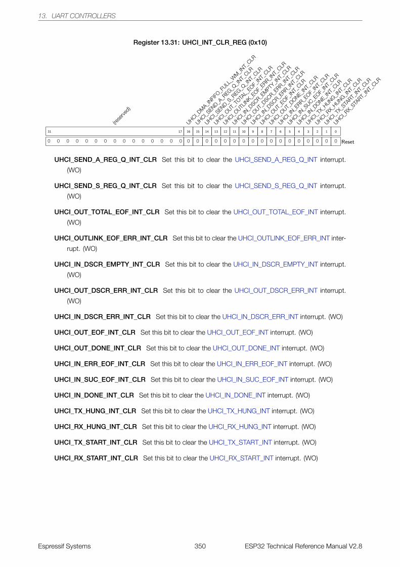
13. UART CONTROLLERS
Register 13.31: UHCI_INT_CLR_REG (0x10)
(rese
rved)
0 0 0 0 0 0 0 0 0 0 0 0 0 0 0
31 17
UHCI_DM
A_INFIF
O_FULL
_WM
_INT_
CLR
0
16
UHCI_SEND_A
_REG_Q
_INT_
CLR
0
15
UHCI_SEND_S
_REG_Q
_INT_
CLR
0
14
UHCI_OUT_
TOTA
L_EOF_
INT_
CLR
0
13
UHCI_OUTL
INK_E
OF_ERR_IN
T_CLR
0
12
UHCI_IN_D
SCR_EM
PTY_IN
T_CLR
0
11
UHCI_OUT_
DSCR_ERR_IN
T_CLR
0
10
UHCI_IN_D
SCR_ERR_IN
T_CLR
0
9
UHCI_OUT_
EOF_IN
T_CLR
0
8
UHCI_OUT_
DONE_INT_
CLR
0
7
UHCI_IN_E
RR_EOF_
INT_
CLR
0
6
UHCI_IN_S
UC_EOF_
INT_
CLR
0
5
UHCI_IN_D
ONE_INT_
CLR
0
4
UHCI_TX_
HUNG_INT_
CLR
0
3
UHCI_RX_
HUNG_INT_
CLR
0
2
UHCI_TX_
START_
INT_
CLR
0
1
UHCI_RX_
START_
INT_
CLR
0
0
Reset
UHCI_SEND_A_REG_Q_INT_CLR Set this bit to clear the UHCI_SEND_A_REG_Q_INT interrupt.
(WO)
UHCI_SEND_S_REG_Q_INT_CLR Set this bit to clear the UHCI_SEND_S_REG_Q_INT interrupt.
(WO)
UHCI_OUT_TOTAL_EOF_INT_CLR Set this bit to clear the UHCI_OUT_TOTAL_EOF_INT interrupt.
(WO)
UHCI_OUTLINK_EOF_ERR_INT_CLR Set this bit to clear the UHCI_OUTLINK_EOF_ERR_INT inter-
rupt. (WO)
UHCI_IN_DSCR_EMPTY_INT_CLR Set this bit to clear the UHCI_IN_DSCR_EMPTY_INT interrupt.
(WO)
UHCI_OUT_DSCR_ERR_INT_CLR Set this bit to clear the UHCI_OUT_DSCR_ERR_INT interrupt.
(WO)
UHCI_IN_DSCR_ERR_INT_CLR Set this bit to clear the UHCI_IN_DSCR_ERR_INT interrupt. (WO)
UHCI_OUT_EOF_INT_CLR Set this bit to clear the UHCI_OUT_EOF_INT interrupt. (WO)
UHCI_OUT_DONE_INT_CLR Set this bit to clear the UHCI_OUT_DONE_INT interrupt. (WO)
UHCI_IN_ERR_EOF_INT_CLR Set this bit to clear the UHCI_IN_ERR_EOF_INT interrupt. (WO)
UHCI_IN_SUC_EOF_INT_CLR Set this bit to clear the UHCI_IN_SUC_EOF_INT interrupt. (WO)
UHCI_IN_DONE_INT_CLR Set this bit to clear the UHCI_IN_DONE_INT interrupt. (WO)
UHCI_TX_HUNG_INT_CLR Set this bit to clear the UHCI_TX_HUNG_INT interrupt. (WO)
UHCI_RX_HUNG_INT_CLR Set this bit to clear the UHCI_RX_HUNG_INT interrupt. (WO)
UHCI_TX_START_INT_CLR Set this bit to clear the UHCI_TX_START_INT interrupt. (WO)
UHCI_RX_START_INT_CLR Set this bit to clear the UHCI_RX_START_INT interrupt. (WO)
Espressif Systems 350 ESP32 Technical Reference Manual V2.8
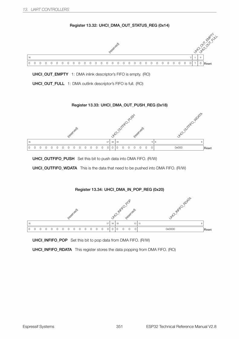
13. UART CONTROLLERS
Register 13.32: UHCI_DMA_OUT_STATUS_REG (0x14)
(rese
rved)
0 0 0 0 0 0 0 0 0 0 0 0 0 0 0 0 0 0 0 0 0 0 0 0 0 0 0 0 0 0
31 2
UHCI_OUT_
EMPTY
1
1
UHCI_OUT_
FULL
0
0
Reset
UHCI_OUT_EMPTY 1: DMA inlink descriptor’s FIFO is empty. (RO)
UHCI_OUT_FULL 1: DMA outlink descriptor’s FIFO is full. (RO)
Register 13.33: UHCI_DMA_OUT_PUSH_REG (0x18)
(rese
rved)
0 0 0 0 0 0 0 0 0 0 0 0 0 0 0
31 17
UHCI_OUTF
IFO_P
USH
0
16
(rese
rved)
0 0 0 0 0 0 0
15 9
UHCI_OUTF
IFO_W
DATA
0x000
8 0
Reset
UHCI_OUTFIFO_PUSH Set this bit to push data into DMA FIFO. (R/W)
UHCI_OUTFIFO_WDATA This is the data that need to be pushed into DMA FIFO. (R/W)
Register 13.34: UHCI_DMA_IN_POP_REG (0x20)
(rese
rved)
0 0 0 0 0 0 0 0 0 0 0 0 0 0 0
31 17
UHCI_INFIF
O_POP
0
16
(rese
rved)
0 0 0 0
15 12
UHCI_INFIF
O_RDAT
A
0x0000
11 0
Reset
UHCI_INFIFO_POP Set this bit to pop data from DMA FIFO. (R/W)
UHCI_INFIFO_RDATA This register stores the data popping from DMA FIFO. (RO)
Espressif Systems 351 ESP32 Technical Reference Manual V2.8
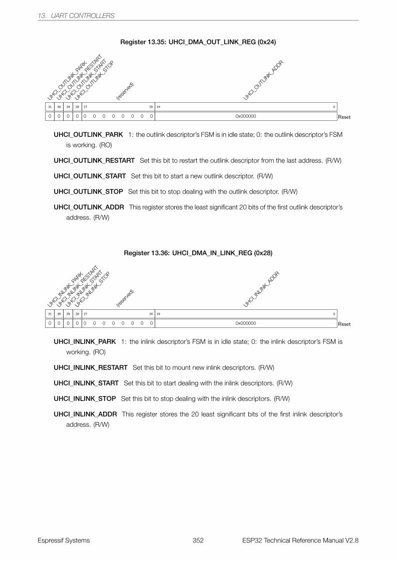
13. UART CONTROLLERS
Register 13.35: UHCI_DMA_OUT_LINK_REG (0x24)
UHCI_OUTL
INK_P
ARK
0
31
UHCI_OUTL
INK_R
ESTART
0
30
UHCI_OUTL
INK_S
TART
0
29
UHCI_OUTL
INK_S
TOP
0
28
(rese
rved)
0 0 0 0 0 0 0 0
27 20
UHCI_OUTL
INK_A
DDR
0x000000
19 0
Reset
UHCI_OUTLINK_PARK 1: the outlink descriptor’s FSM is in idle state; 0: the outlink descriptor’s FSM
is working. (RO)
UHCI_OUTLINK_RESTART Set this bit to restart the outlink descriptor from the last address. (R/W)
UHCI_OUTLINK_START Set this bit to start a new outlink descriptor. (R/W)
UHCI_OUTLINK_STOP Set this bit to stop dealing with the outlink descriptor. (R/W)
UHCI_OUTLINK_ADDR This register stores the least significant 20 bits of the first outlink descriptor’s
address. (R/W)
Register 13.36: UHCI_DMA_IN_LINK_REG (0x28)
UHCI_INLIN
K_PARK
0
31
UHCI_INLIN
K_RESTA
RT
0
30
UHCI_INLIN
K_STA
RT
0
29
UHCI_INLIN
K_STO
P
0
28
(rese
rved)
0 0 0 0 0 0 0 0
27 20
UHCI_INLIN
K_ADDR
0x000000
19 0
Reset
UHCI_INLINK_PARK 1: the inlink descriptor’s FSM is in idle state; 0: the inlink descriptor’s FSM is
working. (RO)
UHCI_INLINK_RESTART Set this bit to mount new inlink descriptors. (R/W)
UHCI_INLINK_START Set this bit to start dealing with the inlink descriptors. (R/W)
UHCI_INLINK_STOP Set this bit to stop dealing with the inlink descriptors. (R/W)
UHCI_INLINK_ADDR This register stores the 20 least significant bits of the first inlink descriptor’s
address. (R/W)
Espressif Systems 352 ESP32 Technical Reference Manual V2.8
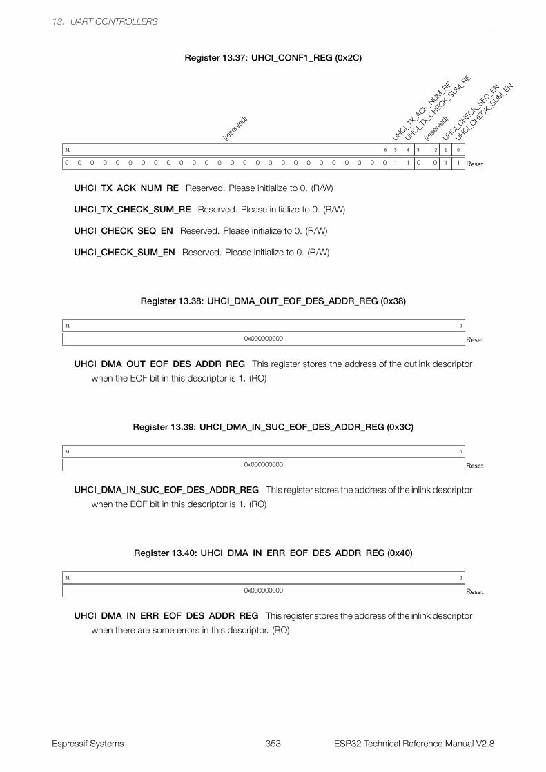
13. UART CONTROLLERS
Register 13.37: UHCI_CONF1_REG (0x2C)
(rese
rved)
0 0 0 0 0 0 0 0 0 0 0 0 0 0 0 0 0 0 0 0 0 0 0 0 0 0
31 6
UHCI_TX_
ACK_NUM
_RE
1
5
UHCI_TX_
CHECK_SUM
_RE
1
4
(rese
rved)
0 0
3 2
UHCI_CHECK_S
EQ_EN
1
1
UHCI_CHECK_S
UM_E
N
1
0
Reset
UHCI_TX_ACK_NUM_RE Reserved. Please initialize to 0. (R/W)
UHCI_TX_CHECK_SUM_RE Reserved. Please initialize to 0. (R/W)
UHCI_CHECK_SEQ_EN Reserved. Please initialize to 0. (R/W)
UHCI_CHECK_SUM_EN Reserved. Please initialize to 0. (R/W)
Register 13.38: UHCI_DMA_OUT_EOF_DES_ADDR_REG (0x38)
0x000000000
31 0
Reset
UHCI_DMA_OUT_EOF_DES_ADDR_REG This register stores the address of the outlink descriptor
when the EOF bit in this descriptor is 1. (RO)
Register 13.39: UHCI_DMA_IN_SUC_EOF_DES_ADDR_REG (0x3C)
0x000000000
31 0
Reset
UHCI_DMA_IN_SUC_EOF_DES_ADDR_REG This register stores the address of the inlink descriptor
when the EOF bit in this descriptor is 1. (RO)
Register 13.40: UHCI_DMA_IN_ERR_EOF_DES_ADDR_REG (0x40)
0x000000000
31 0
Reset
UHCI_DMA_IN_ERR_EOF_DES_ADDR_REG This register stores the address of the inlink descriptor
when there are some errors in this descriptor. (RO)
Espressif Systems 353 ESP32 Technical Reference Manual V2.8
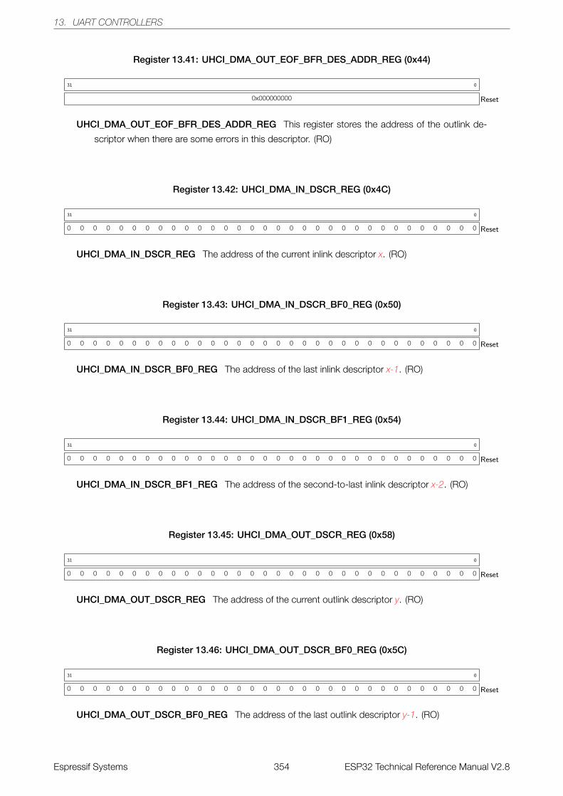
13. UART CONTROLLERS
Register 13.41: UHCI_DMA_OUT_EOF_BFR_DES_ADDR_REG (0x44)
0x000000000
31 0
Reset
UHCI_DMA_OUT_EOF_BFR_DES_ADDR_REG This register stores the address of the outlink de-
scriptor when there are some errors in this descriptor. (RO)
Register 13.42: UHCI_DMA_IN_DSCR_REG (0x4C)
0 0 0 0 0 0 0 0 0 0 0 0 0 0 0 0 0 0 0 0 0 0 0 0 0 0 0 0 0 0 0 0
31 0
Reset
UHCI_DMA_IN_DSCR_REG The address of the current inlink descriptor x. (RO)
Register 13.43: UHCI_DMA_IN_DSCR_BF0_REG (0x50)
0 0 0 0 0 0 0 0 0 0 0 0 0 0 0 0 0 0 0 0 0 0 0 0 0 0 0 0 0 0 0 0
31 0
Reset
UHCI_DMA_IN_DSCR_BF0_REG The address of the last inlink descriptor x-1. (RO)
Register 13.44: UHCI_DMA_IN_DSCR_BF1_REG (0x54)
0 0 0 0 0 0 0 0 0 0 0 0 0 0 0 0 0 0 0 0 0 0 0 0 0 0 0 0 0 0 0 0
31 0
Reset
UHCI_DMA_IN_DSCR_BF1_REG The address of the second-to-last inlink descriptor x-2. (RO)
Register 13.45: UHCI_DMA_OUT_DSCR_REG (0x58)
0 0 0 0 0 0 0 0 0 0 0 0 0 0 0 0 0 0 0 0 0 0 0 0 0 0 0 0 0 0 0 0
31 0
Reset
UHCI_DMA_OUT_DSCR_REG The address of the current outlink descriptor y. (RO)
Register 13.46: UHCI_DMA_OUT_DSCR_BF0_REG (0x5C)
0 0 0 0 0 0 0 0 0 0 0 0 0 0 0 0 0 0 0 0 0 0 0 0 0 0 0 0 0 0 0 0
31 0
Reset
UHCI_DMA_OUT_DSCR_BF0_REG The address of the last outlink descriptor y-1. (RO)
Espressif Systems 354 ESP32 Technical Reference Manual V2.8
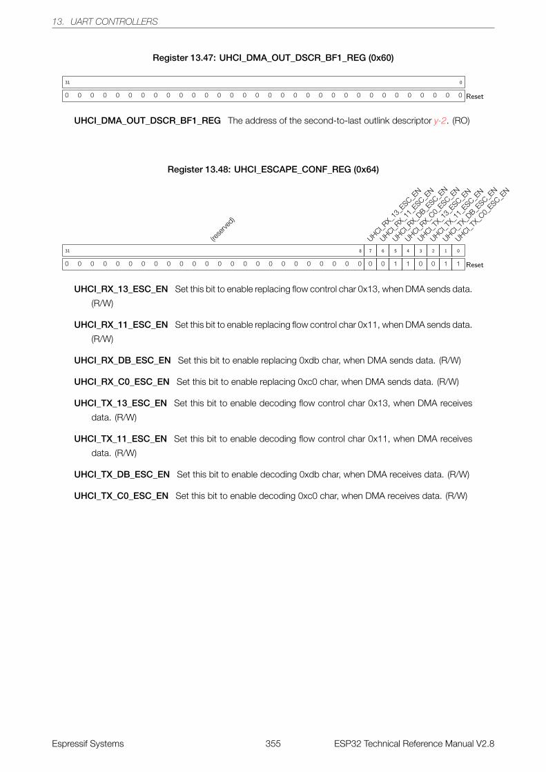
13. UART CONTROLLERS
Register 13.47: UHCI_DMA_OUT_DSCR_BF1_REG (0x60)
0 0 0 0 0 0 0 0 0 0 0 0 0 0 0 0 0 0 0 0 0 0 0 0 0 0 0 0 0 0 0 0
31 0
Reset
UHCI_DMA_OUT_DSCR_BF1_REG The address of the second-to-last outlink descriptor y-2. (RO)
Register 13.48: UHCI_ESCAPE_CONF_REG (0x64)
(rese
rved)
0 0 0 0 0 0 0 0 0 0 0 0 0 0 0 0 0 0 0 0 0 0 0 0
31 8
UHCI_RX_
13_E
SC_EN
0
7
UHCI_RX_
11_E
SC_EN
0
6
UHCI_RX_
DB_ESC_E
N
1
5
UHCI_RX_
C0_ESC_E
N
1
4
UHCI_TX_
13_E
SC_EN
0
3
UHCI_TX_
11_E
SC_EN
0
2
UHCI_TX_
DB_ESC_E
N
1
1
UHCI_TX_
C0_ESC_E
N
1
0
Reset
UHCI_RX_13_ESC_EN Set this bit to enable replacing flow control char 0x13, when DMA sends data.
(R/W)
UHCI_RX_11_ESC_EN Set this bit to enable replacing flow control char 0x11, when DMA sends data.
(R/W)
UHCI_RX_DB_ESC_EN Set this bit to enable replacing 0xdb char, when DMA sends data. (R/W)
UHCI_RX_C0_ESC_EN Set this bit to enable replacing 0xc0 char, when DMA sends data. (R/W)
UHCI_TX_13_ESC_EN Set this bit to enable decoding flow control char 0x13, when DMA receives
data. (R/W)
UHCI_TX_11_ESC_EN Set this bit to enable decoding flow control char 0x11, when DMA receives
data. (R/W)
UHCI_TX_DB_ESC_EN Set this bit to enable decoding 0xdb char, when DMA receives data. (R/W)
UHCI_TX_C0_ESC_EN Set this bit to enable decoding 0xc0 char, when DMA receives data. (R/W)
Espressif Systems 355 ESP32 Technical Reference Manual V2.8
13. UART CONTROLLERS
Register 13.49: UHCI_HUNG_CONF_REG (0x68)
(rese
rved)
0 0 0 0 0 0 0 0
31 24
UHCI_RXF
IFO_T
IMEOUT_
ENA
1
23
UHCI_RXF
IFO_T
IMEOUT_
SHIFT
0 0 0
22 20
UHCI_RXF
IFO_T
IMEOUT
0x010
19 12
UHCI_TXF
IFO_T
IMEOUT_
ENA
1
11
UHCI_TXF
IFO_T
IMEOUT_
SHIFT
0 0 0
10 8
UHCI_TXF
IFO_T
IMEOUT
0x010
7 0
Reset
UHCI_RXFIFO_TIMEOUT_ENA This is the enable bit for DMA send-data timeout. (R/W)
UHCI_RXFIFO_TIMEOUT_SHIFT The tick count is cleared when its value is equal to or greater than
(17’d8000»reg_rxfifo_timeout_shift). (R/W)
UHCI_RXFIFO_TIMEOUT This register stores the timeout value. When DMA takes more time to read
data from RAM than what this register indicates, it will produce the UHCI_RX_HUNG_INT interrupt.
(R/W)
UHCI_TXFIFO_TIMEOUT_ENA The enable bit for Tx FIFO receive-data timeout (R/W)
UHCI_TXFIFO_TIMEOUT_SHIFT The tick count is cleared when its value is equal to or greater than
(17’d8000»reg_txfifo_timeout_shift). (R/W)
UHCI_TXFIFO_TIMEOUT This register stores the timeout value. When DMA takes more time to
receive data than what this register indicates, it will produce the UHCI_TX_HUNG_INT interrupt.
(R/W)
Register 13.50: UHCI_ESC_CONFn_REG (n: 0-3) (0xB0+4*n)
(rese
rved)
0 0 0 0 0 0 0 0
31 24
UHCI_ESC_S
EQ2_CHAR1
0x0DF
23 16
UHCI_ESC_S
EQ2_CHAR0
0x0DB
15 8
UHCI_ESC_S
EQ2
0x013
7 0
Reset
UHCI_ESC_SEQ2_CHAR1 This register stores the second char used to replace the reg_esc_seq2 in
data. (R/W)
UHCI_ESC_SEQ2_CHAR0 This register stores the first char used to replace the reg_esc_seq2 in
data. (R/W)
UHCI_ESC_SEQ2 This register stores the flow_control char to turn off the flow_control. (R/W)
Espressif Systems 356 ESP32 Technical Reference Manual V2.8
14. LED_PWM
14. LED_PWM
14.1 Introduction
The LED_PWM controller is primarily designed to control the intensity of LEDs, although it can be used to
generate PWM signals for other purposes as well. It has 16 channels which can generate independent
waveforms that can be used to drive RGB LED devices. For maximum flexibility, the high-speed as well as the
low-speed channels can be driven from one of four high-speed/low-speed timers. The PWM controller also has
the ability to automatically increase or decrease the duty cycle gradually, allowing for fades without any processor
interference. To increase resolution, the LED_PWM controller is also able to dither between two values, when a
fractional PWM value is configured.
The LED_PWM controller has eight high-speed and eight low-speed PWM generators. In this document, they will
be referred to as hschn and lschn, respectively. These channels can be driven from four timers which will be
indicated by h_timerx and l_timerx.
14.2 Functional Description
14.2.1 Architecture
Figure 83 shows the architecture of the LED_PWM controller. As can be seen in the figure, the LED_PWM
controller contains eight high-speed and eight low-speed channels. There are four high-speed clock modules for
the high-speed channels, from which one h_timerx can be selected. There are also four low-speed clock
modules for the low-speed channels, from which one l_timerx can be selected.
Figure 83: LED_PWM Architecture
Figure 84 illustrates a PWM channel with its selected timer; in this instance a high-speed channel and associated
high-speed timer.
Figure 84: LED_PWM High-speed Channel Diagram
Espressif Systems 357 ESP32 Technical Reference Manual V2.8
14. LED_PWM
14.2.2 Timers
Figure 85: LED_PWM Divider
A high-speed timer consists of a multiplexer to select one of two clock sources: either REF_TICK or APB_CLK.
For more information on the clock sources, please see Chapter Reset And Clock. The input clock is divided
down by a divider first. The division factor is specified by LEDC_CLK_DIV_NUM_HSTIMERx which contains a
fixed point number: the highest 10 bits represent the integer portion A, while the lowest eight bits contain the
fractional portion B. The effective division factor is as follows:
LEDC_CLK_DIV _NUM_HSTIMERx = A B256
Figure 85 shows the input/output clock when the fractional portion B is not 0. As shown in the firgure, the 256
output clocks consist of B output clocks as result of division by (A+1) divider and (256-B) output clocks as result
of division by A divider. The B output clocks are evenly distributed in the 256 output clocks.
The output clock of the divider is the base clock for the counter which will count up to the value specified in
LEDC_HSTIMERx_DUTY_RES. An overflow interrupt will be generated once the counting value reaches
2LEDC_HSTIMERx_DUTY _RES − 1, at which point the counter restarts counting from 0. It is also possible to
reset, suspend, and read the values of the counter by software.
The output signal of the timer is the 20-bit value generated by the counter. The cycle period of this signal defines
the frequency of the signals of any PWM channels connected to this timer. This frequency depends on both the
division factor of the divider, as well as the range of the counter:
fsig_out =fREF_TICK · (!LEDC_TICK_SEL_HSTIMERx) + fAPB_CLK · LEDC_TICK_SEL_HSTIMERx
LEDC_CLK_DIV_NUM_HSTIMERx · 2LEDC_HSTIMERx_DUTY_RES
The low-speed timers l_timerx on the low-speed channel differ from the high-speed timers h_timerx in two
aspects:
1. Where the high-speed timer clock source can be clocked from REF_TICK or APB_CLK, the low-speed
timers are sourced from either REF_TICK or SLOW_CLOCK. The SLOW_CLOCK source can be either
APB_CLK (80 MHz) or 8 MHz, and can be selected using LEDC_APB_CLK_SEL.
2. The high-speed counter and divider are glitch-free, which means that if the software modifies the maximum
counter or divisor value, the update will come into effect after the next overflow interrupt. In contrast, the
low-speed counter and divider will update these values only when LEDC_LSTIMERx_PARA_UP is set.
14.2.3 Channels
A channel takes the 20-bit value from the counter of the selected high-speed timer and compares it to a set of
two values in order to set the channel output. The first value it is compared to is the content of
Espressif Systems 358 ESP32 Technical Reference Manual V2.8
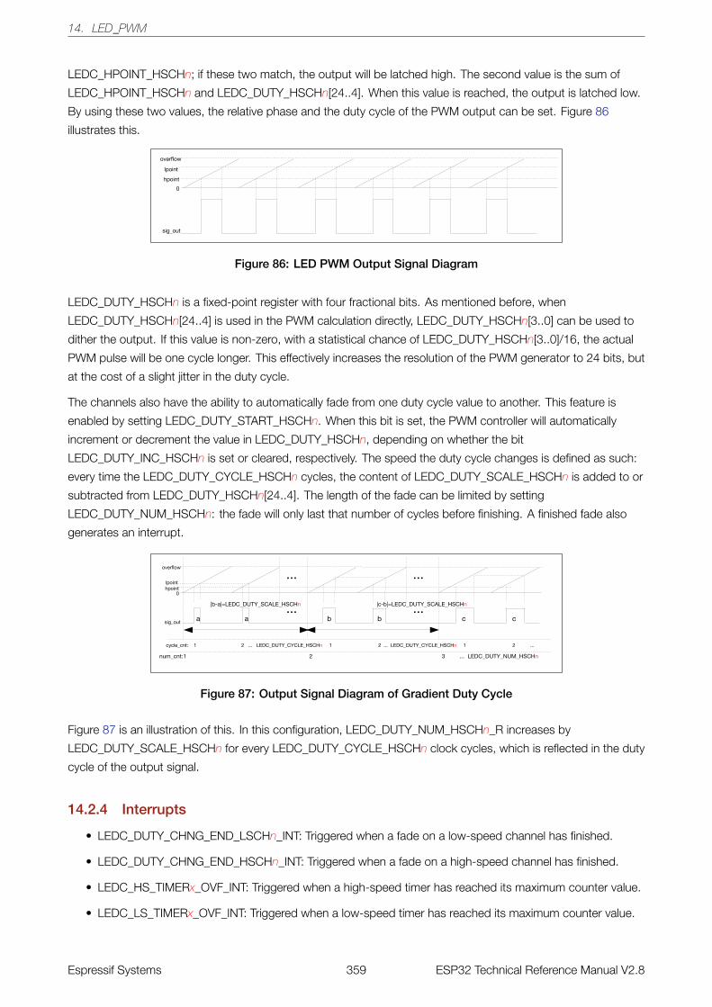
14. LED_PWM
LEDC_HPOINT_HSCHn; if these two match, the output will be latched high. The second value is the sum of
LEDC_HPOINT_HSCHn and LEDC_DUTY_HSCHn[24..4]. When this value is reached, the output is latched low.
By using these two values, the relative phase and the duty cycle of the PWM output can be set. Figure 86
illustrates this.
Figure 86: LED PWM Output Signal Diagram
LEDC_DUTY_HSCHn is a fixed-point register with four fractional bits. As mentioned before, when
LEDC_DUTY_HSCHn[24..4] is used in the PWM calculation directly, LEDC_DUTY_HSCHn[3..0] can be used to
dither the output. If this value is non-zero, with a statistical chance of LEDC_DUTY_HSCHn[3..0]/16, the actual
PWM pulse will be one cycle longer. This effectively increases the resolution of the PWM generator to 24 bits, but
at the cost of a slight jitter in the duty cycle.
The channels also have the ability to automatically fade from one duty cycle value to another. This feature is
enabled by setting LEDC_DUTY_START_HSCHn. When this bit is set, the PWM controller will automatically
increment or decrement the value in LEDC_DUTY_HSCHn, depending on whether the bit
LEDC_DUTY_INC_HSCHn is set or cleared, respectively. The speed the duty cycle changes is defined as such:
every time the LEDC_DUTY_CYCLE_HSCHn cycles, the content of LEDC_DUTY_SCALE_HSCHn is added to or
subtracted from LEDC_DUTY_HSCHn[24..4]. The length of the fade can be limited by setting
LEDC_DUTY_NUM_HSCHn: the fade will only last that number of cycles before finishing. A finished fade also
generates an interrupt.
Figure 87: Output Signal Diagram of Gradient Duty Cycle
Figure 87 is an illustration of this. In this configuration, LEDC_DUTY_NUM_HSCHn_R increases by
LEDC_DUTY_SCALE_HSCHn for every LEDC_DUTY_CYCLE_HSCHn clock cycles, which is reflected in the duty
cycle of the output signal.
14.2.4 Interrupts
• LEDC_DUTY_CHNG_END_LSCHn_INT: Triggered when a fade on a low-speed channel has finished.
• LEDC_DUTY_CHNG_END_HSCHn_INT: Triggered when a fade on a high-speed channel has finished.
• LEDC_HS_TIMERx_OVF_INT: Triggered when a high-speed timer has reached its maximum counter value.
• LEDC_LS_TIMERx_OVF_INT: Triggered when a low-speed timer has reached its maximum counter value.
Espressif Systems 359 ESP32 Technical Reference Manual V2.8
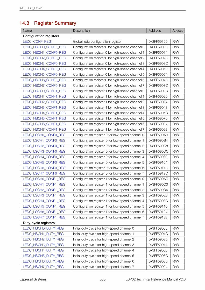
14. LED_PWM
14.3 Register SummaryName Description Address Access
Configuration registers
LEDC_CONF_REG Global ledc configuration register 0x3FF59190 R/W
LEDC_HSCH0_CONF0_REG Configuration register 0 for high-speed channel 0 0x3FF59000 R/W
LEDC_HSCH1_CONF0_REG Configuration register 0 for high-speed channel 1 0x3FF59014 R/W
LEDC_HSCH2_CONF0_REG Configuration register 0 for high-speed channel 2 0x3FF59028 R/W
LEDC_HSCH3_CONF0_REG Configuration register 0 for high-speed channel 3 0x3FF5903C R/W
LEDC_HSCH4_CONF0_REG Configuration register 0 for high-speed channel 4 0x3FF59050 R/W
LEDC_HSCH5_CONF0_REG Configuration register 0 for high-speed channel 5 0x3FF59064 R/W
LEDC_HSCH6_CONF0_REG Configuration register 0 for high-speed channel 6 0x3FF59078 R/W
LEDC_HSCH7_CONF0_REG Configuration register 0 for high-speed channel 7 0x3FF5908C R/W
LEDC_HSCH0_CONF1_REG Configuration register 1 for high-speed channel 0 0x3FF5900C R/W
LEDC_HSCH1_CONF1_REG Configuration register 1 for high-speed channel 1 0x3FF59020 R/W
LEDC_HSCH2_CONF1_REG Configuration register 1 for high-speed channel 2 0x3FF59034 R/W
LEDC_HSCH3_CONF1_REG Configuration register 1 for high-speed channel 3 0x3FF59048 R/W
LEDC_HSCH4_CONF1_REG Configuration register 1 for high-speed channel 4 0x3FF5905C R/W
LEDC_HSCH5_CONF1_REG Configuration register 1 for high-speed channel 5 0x3FF59070 R/W
LEDC_HSCH6_CONF1_REG Configuration register 1 for high-speed channel 6 0x3FF59084 R/W
LEDC_HSCH7_CONF1_REG Configuration register 1 for high-speed channel 7 0x3FF59098 R/W
LEDC_LSCH0_CONF0_REG Configuration register 0 for low-speed channel 0 0x3FF590A0 R/W
LEDC_LSCH1_CONF0_REG Configuration register 0 for low-speed channel 1 0x3FF590B4 R/W
LEDC_LSCH2_CONF0_REG Configuration register 0 for low-speed channel 2 0x3FF590C8 R/W
LEDC_LSCH3_CONF0_REG Configuration register 0 for low-speed channel 3 0x3FF590DC R/W
LEDC_LSCH4_CONF0_REG Configuration register 0 for low-speed channel 4 0x3FF590F0 R/W
LEDC_LSCH5_CONF0_REG Configuration register 0 for low-speed channel 5 0x3FF59104 R/W
LEDC_LSCH6_CONF0_REG Configuration register 0 for low-speed channel 6 0x3FF59118 R/W
LEDC_LSCH7_CONF0_REG Configuration register 0 for low-speed channel 7 0x3FF5912C R/W
LEDC_LSCH0_CONF1_REG Configuration register 1 for low-speed channel 0 0x3FF590AC R/W
LEDC_LSCH1_CONF1_REG Configuration register 1 for low-speed channel 1 0x3FF590C0 R/W
LEDC_LSCH2_CONF1_REG Configuration register 1 for low-speed channel 2 0x3FF590D4 R/W
LEDC_LSCH3_CONF1_REG Configuration register 1 for low-speed channel 3 0x3FF590E8 R/W
LEDC_LSCH4_CONF1_REG Configuration register 1 for low-speed channel 4 0x3FF590FC R/W
LEDC_LSCH5_CONF1_REG Configuration register 1 for low-speed channel 5 0x3FF59110 R/W
LEDC_LSCH6_CONF1_REG Configuration register 1 for low-speed channel 6 0x3FF59124 R/W
LEDC_LSCH7_CONF1_REG Configuration register 1 for low-speed channel 7 0x3FF59138 R/W
Duty-cycle registers
LEDC_HSCH0_DUTY_REG Initial duty cycle for high-speed channel 0 0x3FF59008 R/W
LEDC_HSCH1_DUTY_REG Initial duty cycle for high-speed channel 1 0x3FF5901C R/W
LEDC_HSCH2_DUTY_REG Initial duty cycle for high-speed channel 2 0x3FF59030 R/W
LEDC_HSCH3_DUTY_REG Initial duty cycle for high-speed channel 3 0x3FF59044 R/W
LEDC_HSCH4_DUTY_REG Initial duty cycle for high-speed channel 4 0x3FF59058 R/W
LEDC_HSCH5_DUTY_REG Initial duty cycle for high-speed channel 5 0x3FF5906C R/W
LEDC_HSCH6_DUTY_REG Initial duty cycle for high-speed channel 6 0x3FF59080 R/W
LEDC_HSCH7_DUTY_REG Initial duty cycle for high-speed channel 7 0x3FF59094 R/W
Espressif Systems 360 ESP32 Technical Reference Manual V2.8
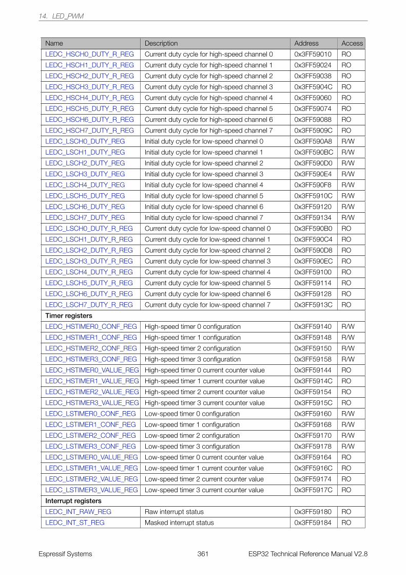
14. LED_PWM
Name Description Address Access
LEDC_HSCH0_DUTY_R_REG Current duty cycle for high-speed channel 0 0x3FF59010 RO
LEDC_HSCH1_DUTY_R_REG Current duty cycle for high-speed channel 1 0x3FF59024 RO
LEDC_HSCH2_DUTY_R_REG Current duty cycle for high-speed channel 2 0x3FF59038 RO
LEDC_HSCH3_DUTY_R_REG Current duty cycle for high-speed channel 3 0x3FF5904C RO
LEDC_HSCH4_DUTY_R_REG Current duty cycle for high-speed channel 4 0x3FF59060 RO
LEDC_HSCH5_DUTY_R_REG Current duty cycle for high-speed channel 5 0x3FF59074 RO
LEDC_HSCH6_DUTY_R_REG Current duty cycle for high-speed channel 6 0x3FF59088 RO
LEDC_HSCH7_DUTY_R_REG Current duty cycle for high-speed channel 7 0x3FF5909C RO
LEDC_LSCH0_DUTY_REG Initial duty cycle for low-speed channel 0 0x3FF590A8 R/W
LEDC_LSCH1_DUTY_REG Initial duty cycle for low-speed channel 1 0x3FF590BC R/W
LEDC_LSCH2_DUTY_REG Initial duty cycle for low-speed channel 2 0x3FF590D0 R/W
LEDC_LSCH3_DUTY_REG Initial duty cycle for low-speed channel 3 0x3FF590E4 R/W
LEDC_LSCH4_DUTY_REG Initial duty cycle for low-speed channel 4 0x3FF590F8 R/W
LEDC_LSCH5_DUTY_REG Initial duty cycle for low-speed channel 5 0x3FF5910C R/W
LEDC_LSCH6_DUTY_REG Initial duty cycle for low-speed channel 6 0x3FF59120 R/W
LEDC_LSCH7_DUTY_REG Initial duty cycle for low-speed channel 7 0x3FF59134 R/W
LEDC_LSCH0_DUTY_R_REG Current duty cycle for low-speed channel 0 0x3FF590B0 RO
LEDC_LSCH1_DUTY_R_REG Current duty cycle for low-speed channel 1 0x3FF590C4 RO
LEDC_LSCH2_DUTY_R_REG Current duty cycle for low-speed channel 2 0x3FF590D8 RO
LEDC_LSCH3_DUTY_R_REG Current duty cycle for low-speed channel 3 0x3FF590EC RO
LEDC_LSCH4_DUTY_R_REG Current duty cycle for low-speed channel 4 0x3FF59100 RO
LEDC_LSCH5_DUTY_R_REG Current duty cycle for low-speed channel 5 0x3FF59114 RO
LEDC_LSCH6_DUTY_R_REG Current duty cycle for low-speed channel 6 0x3FF59128 RO
LEDC_LSCH7_DUTY_R_REG Current duty cycle for low-speed channel 7 0x3FF5913C RO
Timer registers
LEDC_HSTIMER0_CONF_REG High-speed timer 0 configuration 0x3FF59140 R/W
LEDC_HSTIMER1_CONF_REG High-speed timer 1 configuration 0x3FF59148 R/W
LEDC_HSTIMER2_CONF_REG High-speed timer 2 configuration 0x3FF59150 R/W
LEDC_HSTIMER3_CONF_REG High-speed timer 3 configuration 0x3FF59158 R/W
LEDC_HSTIMER0_VALUE_REG High-speed timer 0 current counter value 0x3FF59144 RO
LEDC_HSTIMER1_VALUE_REG High-speed timer 1 current counter value 0x3FF5914C RO
LEDC_HSTIMER2_VALUE_REG High-speed timer 2 current counter value 0x3FF59154 RO
LEDC_HSTIMER3_VALUE_REG High-speed timer 3 current counter value 0x3FF5915C RO
LEDC_LSTIMER0_CONF_REG Low-speed timer 0 configuration 0x3FF59160 R/W
LEDC_LSTIMER1_CONF_REG Low-speed timer 1 configuration 0x3FF59168 R/W
LEDC_LSTIMER2_CONF_REG Low-speed timer 2 configuration 0x3FF59170 R/W
LEDC_LSTIMER3_CONF_REG Low-speed timer 3 configuration 0x3FF59178 R/W
LEDC_LSTIMER0_VALUE_REG Low-speed timer 0 current counter value 0x3FF59164 RO
LEDC_LSTIMER1_VALUE_REG Low-speed timer 1 current counter value 0x3FF5916C RO
LEDC_LSTIMER2_VALUE_REG Low-speed timer 2 current counter value 0x3FF59174 RO
LEDC_LSTIMER3_VALUE_REG Low-speed timer 3 current counter value 0x3FF5917C RO
Interrupt registers
LEDC_INT_RAW_REG Raw interrupt status 0x3FF59180 RO
LEDC_INT_ST_REG Masked interrupt status 0x3FF59184 RO
Espressif Systems 361 ESP32 Technical Reference Manual V2.8
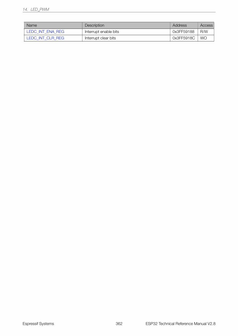
14. LED_PWM
Name Description Address Access
LEDC_INT_ENA_REG Interrupt enable bits 0x3FF59188 R/W
LEDC_INT_CLR_REG Interrupt clear bits 0x3FF5918C WO
Espressif Systems 362 ESP32 Technical Reference Manual V2.8
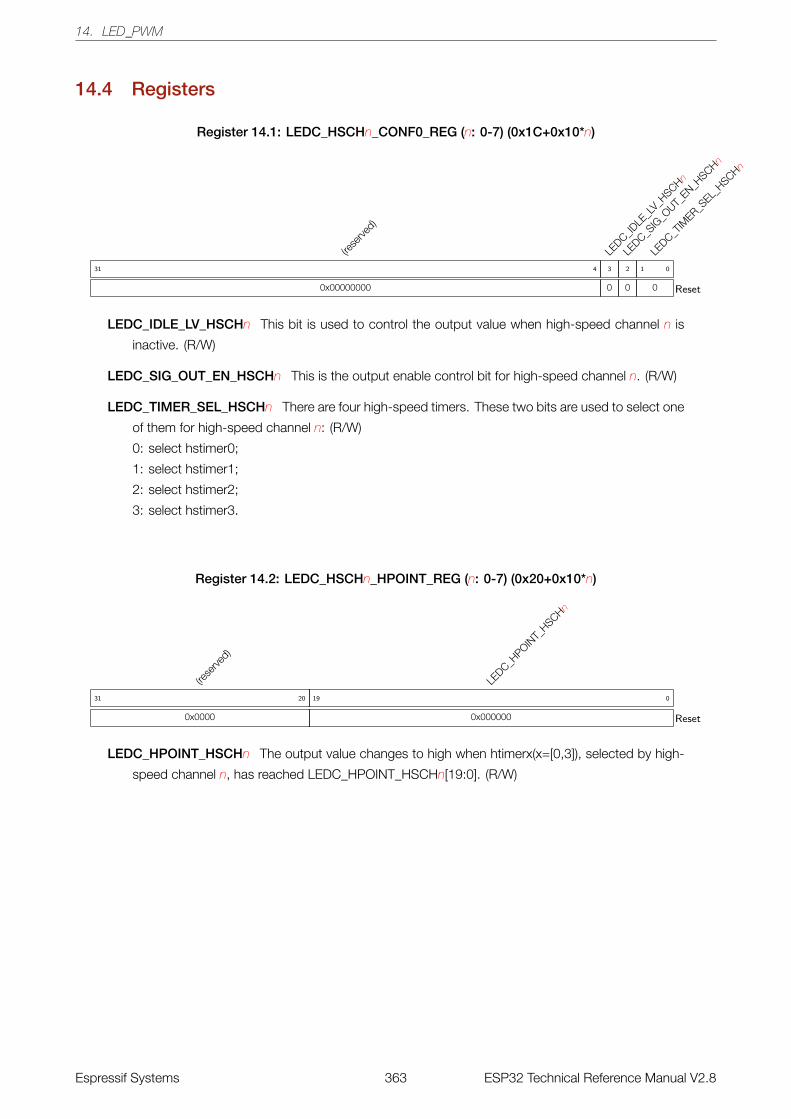
14. LED_PWM
14.4 Registers
Register 14.1: LEDC_HSCHn_CONF0_REG (n: 0-7) (0x1C+0x10*n)
(rese
rved)
0x00000000
31 4
LEDC_ID
LE_L
V_HSCHn
0
3
LEDC_S
IG_O
UT_EN_H
SCHn
0
2
LEDC_T
IMER_S
EL_HSCHn
0
1 0
Reset
LEDC_IDLE_LV_HSCHn This bit is used to control the output value when high-speed channel n is
inactive. (R/W)
LEDC_SIG_OUT_EN_HSCHn This is the output enable control bit for high-speed channel n. (R/W)
LEDC_TIMER_SEL_HSCHn There are four high-speed timers. These two bits are used to select one
of them for high-speed channel n: (R/W)
0: select hstimer0;
1: select hstimer1;
2: select hstimer2;
3: select hstimer3.
Register 14.2: LEDC_HSCHn_HPOINT_REG (n: 0-7) (0x20+0x10*n)
(rese
rved)
0x0000
31 20
LEDC_H
POINT_
HSCHn
0x000000
19 0
Reset
LEDC_HPOINT_HSCHn The output value changes to high when htimerx(x=[0,3]), selected by high-
speed channel n, has reached LEDC_HPOINT_HSCHn[19:0]. (R/W)
Espressif Systems 363 ESP32 Technical Reference Manual V2.8
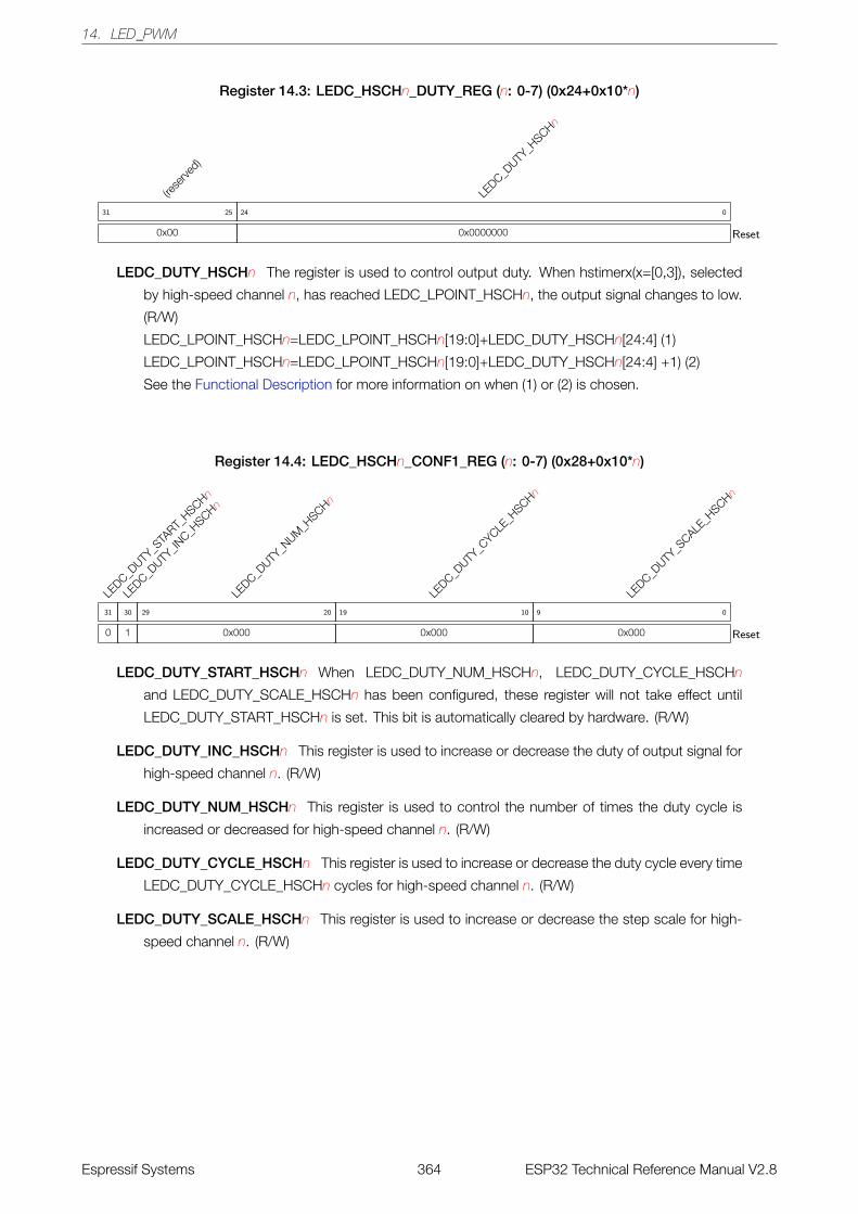
14. LED_PWM
Register 14.3: LEDC_HSCHn_DUTY_REG (n: 0-7) (0x24+0x10*n)
(rese
rved)
0x00
31 25
LEDC_D
UTY_H
SCHn
0x0000000
24 0
Reset
LEDC_DUTY_HSCHn The register is used to control output duty. When hstimerx(x=[0,3]), selected
by high-speed channel n, has reached LEDC_LPOINT_HSCHn, the output signal changes to low.
(R/W)
LEDC_LPOINT_HSCHn=LEDC_LPOINT_HSCHn[19:0]+LEDC_DUTY_HSCHn[24:4] (1)
LEDC_LPOINT_HSCHn=LEDC_LPOINT_HSCHn[19:0]+LEDC_DUTY_HSCHn[24:4] +1) (2)
See the Functional Description for more information on when (1) or (2) is chosen.
Register 14.4: LEDC_HSCHn_CONF1_REG (n: 0-7) (0x28+0x10*n)
LEDC_D
UTY_S
TART_
HSCHn
0
31
LEDC_D
UTY_IN
C_HSCHn
1
30
LEDC_D
UTY_N
UM_H
SCHn
0x000
29 20
LEDC_D
UTY_C
YCLE_H
SCHn
0x000
19 10
LEDC_D
UTY_S
CALE_H
SCHn
0x000
9 0
Reset
LEDC_DUTY_START_HSCHn When LEDC_DUTY_NUM_HSCHn, LEDC_DUTY_CYCLE_HSCHn
and LEDC_DUTY_SCALE_HSCHn has been configured, these register will not take effect until
LEDC_DUTY_START_HSCHn is set. This bit is automatically cleared by hardware. (R/W)
LEDC_DUTY_INC_HSCHn This register is used to increase or decrease the duty of output signal for
high-speed channel n. (R/W)
LEDC_DUTY_NUM_HSCHn This register is used to control the number of times the duty cycle is
increased or decreased for high-speed channel n. (R/W)
LEDC_DUTY_CYCLE_HSCHn This register is used to increase or decrease the duty cycle every time
LEDC_DUTY_CYCLE_HSCHn cycles for high-speed channel n. (R/W)
LEDC_DUTY_SCALE_HSCHn This register is used to increase or decrease the step scale for high-
speed channel n. (R/W)
Espressif Systems 364 ESP32 Technical Reference Manual V2.8
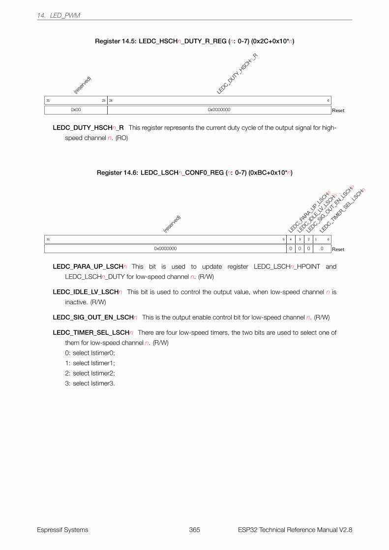
14. LED_PWM
Register 14.5: LEDC_HSCHn_DUTY_R_REG (n: 0-7) (0x2C+0x10*n)
(rese
rved)
0x00
31 25
LEDC_D
UTY_H
SCHn_R
0x0000000
24 0
Reset
LEDC_DUTY_HSCHn_R This register represents the current duty cycle of the output signal for high-
speed channel n. (RO)
Register 14.6: LEDC_LSCHn_CONF0_REG (n: 0-7) (0xBC+0x10*n)
(rese
rved)
0x0000000
31 5
LEDC_P
ARA_UP_L
SCHn
0
4
LEDC_ID
LE_L
V_LSCHn
0
3
LEDC_S
IG_O
UT_EN_L
SCHn
0
2
LEDC_T
IMER_S
EL_LS
CHn
0
1 0
Reset
LEDC_PARA_UP_LSCHn This bit is used to update register LEDC_LSCHn_HPOINT and
LEDC_LSCHn_DUTY for low-speed channel n. (R/W)
LEDC_IDLE_LV_LSCHn This bit is used to control the output value, when low-speed channel n is
inactive. (R/W)
LEDC_SIG_OUT_EN_LSCHn This is the output enable control bit for low-speed channel n. (R/W)
LEDC_TIMER_SEL_LSCHn There are four low-speed timers, the two bits are used to select one of
them for low-speed channel n. (R/W)
0: select lstimer0;
1: select lstimer1;
2: select lstimer2;
3: select lstimer3.
Espressif Systems 365 ESP32 Technical Reference Manual V2.8
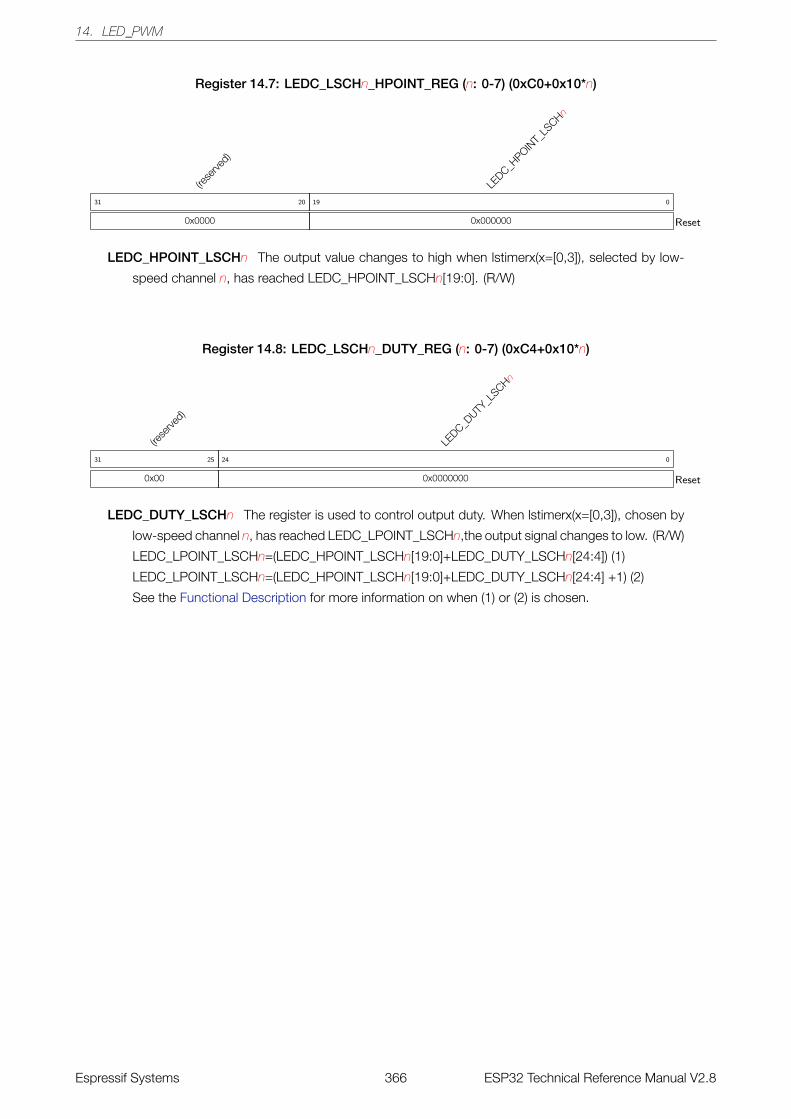
14. LED_PWM
Register 14.7: LEDC_LSCHn_HPOINT_REG (n: 0-7) (0xC0+0x10*n)
(rese
rved)
0x0000
31 20
LEDC_H
POINT_
LSCHn
0x000000
19 0
Reset
LEDC_HPOINT_LSCHn The output value changes to high when lstimerx(x=[0,3]), selected by low-
speed channel n, has reached LEDC_HPOINT_LSCHn[19:0]. (R/W)
Register 14.8: LEDC_LSCHn_DUTY_REG (n: 0-7) (0xC4+0x10*n)
(rese
rved)
0x00
31 25
LEDC_D
UTY_L
SCHn
0x0000000
24 0
Reset
LEDC_DUTY_LSCHn The register is used to control output duty. When lstimerx(x=[0,3]), chosen by
low-speed channel n, has reached LEDC_LPOINT_LSCHn,the output signal changes to low. (R/W)
LEDC_LPOINT_LSCHn=(LEDC_HPOINT_LSCHn[19:0]+LEDC_DUTY_LSCHn[24:4]) (1)
LEDC_LPOINT_LSCHn=(LEDC_HPOINT_LSCHn[19:0]+LEDC_DUTY_LSCHn[24:4] +1) (2)
See the Functional Description for more information on when (1) or (2) is chosen.
Espressif Systems 366 ESP32 Technical Reference Manual V2.8
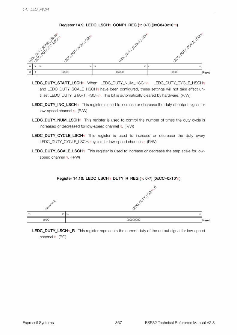
14. LED_PWM
Register 14.9: LEDC_LSCHn_CONF1_REG (n: 0-7) (0xC8+0x10*n)
LEDC_D
UTY_S
TART_
LSCHn
0
31
LEDC_D
UTY_IN
C_LSCHn
1
30
LEDC_D
UTY_N
UM_L
SCHn
0x000
29 20
LEDC_D
UTY_C
YCLE_L
SCHn
0x000
19 10
LEDC_D
UTY_S
CALE_L
SCHn
0x000
9 0
Reset
LEDC_DUTY_START_LSCHn When LEDC_DUTY_NUM_HSCHn, LEDC_DUTY_CYCLE_HSCHn
and LEDC_DUTY_SCALE_HSCHn have been configured, these settings will not take effect un-
til set LEDC_DUTY_START_HSCHn. This bit is automatically cleared by hardware. (R/W)
LEDC_DUTY_INC_LSCHn This register is used to increase or decrease the duty of output signal for
low-speed channel n. (R/W)
LEDC_DUTY_NUM_LSCHn This register is used to control the number of times the duty cycle is
increased or decreased for low-speed channel n. (R/W)
LEDC_DUTY_CYCLE_LSCHn This register is used to increase or decrease the duty every
LEDC_DUTY_CYCLE_LSCHn cycles for low-speed channel n. (R/W)
LEDC_DUTY_SCALE_LSCHn This register is used to increase or decrease the step scale for low-
speed channel n. (R/W)
Register 14.10: LEDC_LSCHn_DUTY_R_REG (n: 0-7) (0xCC+0x10*n)
(rese
rved)
0x00
31 25
LEDC_D
UTY_L
SCHn_R
0x0000000
24 0
Reset
LEDC_DUTY_LSCHn_R This register represents the current duty of the output signal for low-speed
channel n. (RO)
Espressif Systems 367 ESP32 Technical Reference Manual V2.8
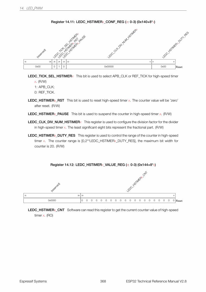
14. LED_PWM
Register 14.11: LEDC_HSTIMERx_CONF_REG (x: 0-3) (0x140+8*x)
(rese
rved)
0x00
31 26
LEDC_T
ICK_S
EL_HSTIM
ERx
0
25
LEDC_H
STIMERx
_RST
1
24
LEDC_H
STIMERx
_PAUSE
0
23
LEDC_C
LK_D
IV_NUM
_HSTIM
ERx
0x00000
22 5
LEDC_H
STIMERx
_DUTY
_RES
0x00
4 0
Reset
LEDC_TICK_SEL_HSTIMERx This bit is used to select APB_CLK or REF_TICK for high-speed timer
x. (R/W)
1: APB_CLK;
0: REF_TICK.
LEDC_HSTIMERx_RST This bit is used to reset high-speed timer x. The counter value will be ’zero’
after reset. (R/W)
LEDC_HSTIMERx_PAUSE This bit is used to suspend the counter in high-speed timer x. (R/W)
LEDC_CLK_DIV_NUM_HSTIMERx This register is used to configure the division factor for the divider
in high-speed timer x. The least significant eight bits represent the fractional part. (R/W)
LEDC_HSTIMERx_DUTY_RES This register is used to control the range of the counter in high-speed
timer x. The counter range is [0,2**LEDC_HSTIMERx_DUTY_RES], the maximum bit width for
counter is 20. (R/W)
Register 14.12: LEDC_HSTIMERx_VALUE_REG (x: 0-3) (0x144+8*x)
(rese
rved)
0x0000
31 20
LEDC_H
STIMERx
_CNT
0 0 0 0 0 0 0 0 0 0 0 0 0 0 0 0 0 0 0 0
19 0
Reset
LEDC_HSTIMERx_CNT Software can read this register to get the current counter value of high-speed
timer x. (RO)
Espressif Systems 368 ESP32 Technical Reference Manual V2.8
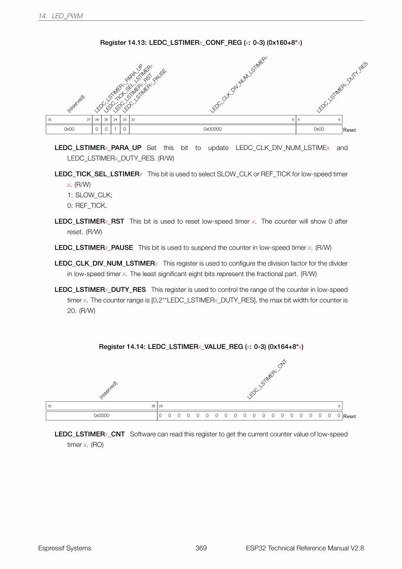
14. LED_PWM
Register 14.13: LEDC_LSTIMERx_CONF_REG (x: 0-3) (0x160+8*x)
(rese
rved)
0x00
31 27
LEDC_L
STIMERx
_PARA_U
P
0
26
LEDC_T
ICK_S
EL_LS
TIMERx
0
25
LEDC_L
STIMERx
_RST
1
24
LEDC_L
STIMERx
_PAUSE
0
23
LEDC_C
LK_D
IV_NUM
_LSTIM
ERx
0x00000
22 5
LEDC_L
STIMERx
_DUTY
_RES
0x00
4 0
Reset
LEDC_LSTIMERx_PARA_UP Set this bit to update LEDC_CLK_DIV_NUM_LSTIMEx and
LEDC_LSTIMERx_DUTY_RES. (R/W)
LEDC_TICK_SEL_LSTIMERx This bit is used to select SLOW_CLK or REF_TICK for low-speed timer
x. (R/W)
1: SLOW_CLK;
0: REF_TICK.
LEDC_LSTIMERx_RST This bit is used to reset low-speed timer x. The counter will show 0 after
reset. (R/W)
LEDC_LSTIMERx_PAUSE This bit is used to suspend the counter in low-speed timer x. (R/W)
LEDC_CLK_DIV_NUM_LSTIMERx This register is used to configure the division factor for the divider
in low-speed timer x. The least significant eight bits represent the fractional part. (R/W)
LEDC_LSTIMERx_DUTY_RES This register is used to control the range of the counter in low-speed
timer x. The counter range is [0,2**LEDC_LSTIMERx_DUTY_RES], the max bit width for counter is
20. (R/W)
Register 14.14: LEDC_LSTIMERx_VALUE_REG (x: 0-3) (0x164+8*x)
(rese
rved)
0x0000
31 20
LEDC_L
STIMERx
_CNT
0 0 0 0 0 0 0 0 0 0 0 0 0 0 0 0 0 0 0 0
19 0
Reset
LEDC_LSTIMERx_CNT Software can read this register to get the current counter value of low-speed
timer x. (RO)
Espressif Systems 369 ESP32 Technical Reference Manual V2.8
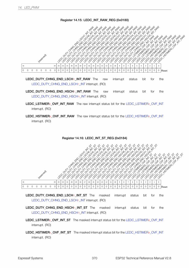
14. LED_PWM
Register 14.15: LEDC_INT_RAW_REG (0x0180)
(rese
rved)
0 0 0 0 0 0 0 0
31 24
LEDC_D
UTY_C
HNG_END_L
SCH7_IN
T_RAW
0
23
LEDC_D
UTY_C
HNG_END_L
SCH6_IN
T_RAW
0
22
LEDC_D
UTY_C
HNG_END_L
SCH5_IN
T_RAW
0
21
LEDC_D
UTY_C
HNG_END_L
SCH4_IN
T_RAW
0
20
LEDC_D
UTY_C
HNG_END_L
SCH3_IN
T_RAW
0
19
LEDC_D
UTY_C
HNG_END_L
SCH2_IN
T_RAW
0
18
LEDC_D
UTY_C
HNG_END_L
SCH1_IN
T_RAW
0
17
LEDC_D
UTY_C
HNG_END_L
SCH0_IN
T_RAW
0
16
LEDC_D
UTY_C
HNG_END_H
SCH7_IN
T_RAW
0
15
LEDC_D
UTY_C
HNG_END_H
SCH6_IN
T_RAW
0
14
LEDC_D
UTY_C
HNG_END_H
SCH5_IN
T_RAW
0
13
LEDC_D
UTY_C
HNG_END_H
SCH4_IN
T_RAW
0
12
LEDC_D
UTY_C
HNG_END_H
SCH3_IN
T_RAW
0
11
LEDC_D
UTY_C
HNG_END_H
SCH2_IN
T_RAW
0
10
LEDC_D
UTY_C
HNG_END_H
SCH1_IN
T_RAW
0
9
LEDC_D
UTY_C
HNG_END_H
SCH0_IN
T_RAW
0
8
LEDC_L
STIMER3_
OVF_IN
T_RAW
0
7
LEDC_L
STIMER2_
OVF_IN
T_RAW
0
6
LEDC_L
STIMER1_
OVF_IN
T_RAW
0
5
LEDC_L
STIMER0_
OVF_IN
T_RAW
0
4
LEDC_H
STIMER3_
OVF_IN
T_RAW
0
3
LEDC_H
STIMER2_
OVF_IN
T_RAW
0
2
LEDC_H
STIMER1_
OVF_IN
T_RAW
0
1
LEDC_H
STIMER0_
OVF_IN
T_RAW
0
0
Reset
LEDC_DUTY_CHNG_END_LSCHn_INT_RAW The raw interrupt status bit for the
LEDC_DUTY_CHNG_END_LSCHn_INT interrupt. (RO)
LEDC_DUTY_CHNG_END_HSCHn_INT_RAW The raw interrupt status bit for the
LEDC_DUTY_CHNG_END_HSCHn_INT interrupt. (RO)
LEDC_LSTIMERx_OVF_INT_RAW The raw interrupt status bit for the LEDC_LSTIMERx_OVF_INT
interrupt. (RO)
LEDC_HSTIMERx_OVF_INT_RAW The raw interrupt status bit for the LEDC_HSTIMERx_OVF_INT
interrupt. (RO)
Register 14.16: LEDC_INT_ST_REG (0x0184)
(rese
rved)
0 0 0 0 0 0 0 0
31 24
LEDC_D
UTY_C
HNG_END_L
SCH7_IN
T_ST
0
23
LEDC_D
UTY_C
HNG_END_L
SCH6_IN
T_ST
0
22
LEDC_D
UTY_C
HNG_END_L
SCH5_IN
T_ST
0
21
LEDC_D
UTY_C
HNG_END_L
SCH4_IN
T_ST
0
20
LEDC_D
UTY_C
HNG_END_L
SCH3_IN
T_ST
0
19
LEDC_D
UTY_C
HNG_END_L
SCH2_IN
T_ST
0
18
LEDC_D
UTY_C
HNG_END_L
SCH1_IN
T_ST
0
17
LEDC_D
UTY_C
HNG_END_L
SCH0_IN
T_ST
0
16
LEDC_D
UTY_C
HNG_END_H
SCH7_IN
T_ST
0
15
LEDC_D
UTY_C
HNG_END_H
SCH6_IN
T_ST
0
14
LEDC_D
UTY_C
HNG_END_H
SCH5_IN
T_ST
0
13
LEDC_D
UTY_C
HNG_END_H
SCH4_IN
T_ST
0
12
LEDC_D
UTY_C
HNG_END_H
SCH3_IN
T_ST
0
11
LEDC_D
UTY_C
HNG_END_H
SCH2_IN
T_ST
0
10
LEDC_D
UTY_C
HNG_END_H
SCH1_IN
T_ST
0
9
LEDC_D
UTY_C
HNG_END_H
SCH0_IN
T_ST
0
8
LEDC_L
STIMER3_
OVF_IN
T_ST
0
7
LEDC_L
STIMER2_
OVF_IN
T_ST
0
6
LEDC_L
STIMER1_
OVF_IN
T_ST
0
5
LEDC_L
STIMER0_
OVF_IN
T_ST
0
4
LEDC_H
STIMER3_
OVF_IN
T_ST
0
3
LEDC_H
STIMER2_
OVF_IN
T_ST
0
2
LEDC_H
STIMER1_
OVF_IN
T_ST
0
1
LEDC_H
STIMER0_
OVF_IN
T_ST
0
0
Reset
LEDC_DUTY_CHNG_END_LSCHn_INT_ST The masked interrupt status bit for the
LEDC_DUTY_CHNG_END_LSCHn_INT interrupt. (RO)
LEDC_DUTY_CHNG_END_HSCHn_INT_ST The masked interrupt status bit for the
LEDC_DUTY_CHNG_END_HSCHn_INT interrupt. (RO)
LEDC_LSTIMERx_OVF_INT_ST The masked interrupt status bit for the LEDC_LSTIMERx_OVF_INT
interrupt. (RO)
LEDC_HSTIMERx_OVF_INT_ST The masked interrupt status bit for the LEDC_HSTIMERx_OVF_INT
interrupt. (RO)
Espressif Systems 370 ESP32 Technical Reference Manual V2.8
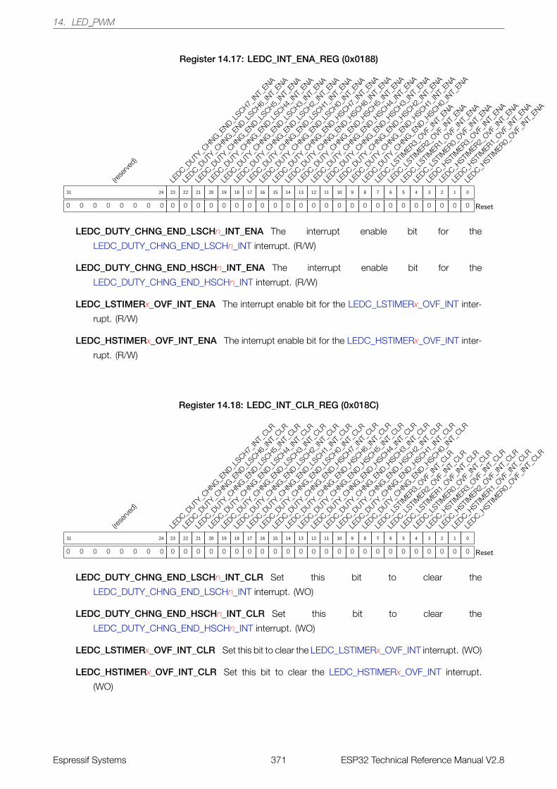
14. LED_PWM
Register 14.17: LEDC_INT_ENA_REG (0x0188)
(rese
rved)
0 0 0 0 0 0 0 0
31 24
LEDC_D
UTY_C
HNG_END_L
SCH7_IN
T_ENA
0
23
LEDC_D
UTY_C
HNG_END_L
SCH6_IN
T_ENA
0
22
LEDC_D
UTY_C
HNG_END_L
SCH5_IN
T_ENA
0
21
LEDC_D
UTY_C
HNG_END_L
SCH4_IN
T_ENA
0
20
LEDC_D
UTY_C
HNG_END_L
SCH3_IN
T_ENA
0
19
LEDC_D
UTY_C
HNG_END_L
SCH2_IN
T_ENA
0
18
LEDC_D
UTY_C
HNG_END_L
SCH1_IN
T_ENA
0
17
LEDC_D
UTY_C
HNG_END_L
SCH0_IN
T_ENA
0
16
LEDC_D
UTY_C
HNG_END_H
SCH7_IN
T_ENA
0
15
LEDC_D
UTY_C
HNG_END_H
SCH6_IN
T_ENA
0
14
LEDC_D
UTY_C
HNG_END_H
SCH5_IN
T_ENA
0
13
LEDC_D
UTY_C
HNG_END_H
SCH4_IN
T_ENA
0
12
LEDC_D
UTY_C
HNG_END_H
SCH3_IN
T_ENA
0
11
LEDC_D
UTY_C
HNG_END_H
SCH2_IN
T_ENA
0
10
LEDC_D
UTY_C
HNG_END_H
SCH1_IN
T_ENA
0
9
LEDC_D
UTY_C
HNG_END_H
SCH0_IN
T_ENA
0
8
LEDC_L
STIMER3_
OVF_IN
T_ENA
0
7
LEDC_L
STIMER2_
OVF_IN
T_ENA
0
6
LEDC_L
STIMER1_
OVF_IN
T_ENA
0
5
LEDC_L
STIMER0_
OVF_IN
T_ENA
0
4
LEDC_H
STIMER3_
OVF_IN
T_ENA
0
3
LEDC_H
STIMER2_
OVF_IN
T_ENA
0
2
LEDC_H
STIMER1_
OVF_IN
T_ENA
0
1
LEDC_H
STIMER0_
OVF_IN
T_ENA
0
0
Reset
LEDC_DUTY_CHNG_END_LSCHn_INT_ENA The interrupt enable bit for the
LEDC_DUTY_CHNG_END_LSCHn_INT interrupt. (R/W)
LEDC_DUTY_CHNG_END_HSCHn_INT_ENA The interrupt enable bit for the
LEDC_DUTY_CHNG_END_HSCHn_INT interrupt. (R/W)
LEDC_LSTIMERx_OVF_INT_ENA The interrupt enable bit for the LEDC_LSTIMERx_OVF_INT inter-
rupt. (R/W)
LEDC_HSTIMERx_OVF_INT_ENA The interrupt enable bit for the LEDC_HSTIMERx_OVF_INT inter-
rupt. (R/W)
Register 14.18: LEDC_INT_CLR_REG (0x018C)
(rese
rved)
0 0 0 0 0 0 0 0
31 24
LEDC_D
UTY_C
HNG_END_L
SCH7_IN
T_CLR
0
23
LEDC_D
UTY_C
HNG_END_L
SCH6_IN
T_CLR
0
22
LEDC_D
UTY_C
HNG_END_L
SCH5_IN
T_CLR
0
21
LEDC_D
UTY_C
HNG_END_L
SCH4_IN
T_CLR
0
20
LEDC_D
UTY_C
HNG_END_L
SCH3_IN
T_CLR
0
19
LEDC_D
UTY_C
HNG_END_L
SCH2_IN
T_CLR
0
18
LEDC_D
UTY_C
HNG_END_L
SCH1_IN
T_CLR
0
17
LEDC_D
UTY_C
HNG_END_L
SCH0_IN
T_CLR
0
16
LEDC_D
UTY_C
HNG_END_H
SCH7_IN
T_CLR
0
15
LEDC_D
UTY_C
HNG_END_H
SCH6_IN
T_CLR
0
14
LEDC_D
UTY_C
HNG_END_H
SCH5_IN
T_CLR
0
13
LEDC_D
UTY_C
HNG_END_H
SCH4_IN
T_CLR
0
12
LEDC_D
UTY_C
HNG_END_H
SCH3_IN
T_CLR
0
11
LEDC_D
UTY_C
HNG_END_H
SCH2_IN
T_CLR
0
10
LEDC_D
UTY_C
HNG_END_H
SCH1_IN
T_CLR
0
9
LEDC_D
UTY_C
HNG_END_H
SCH0_IN
T_CLR
0
8
LEDC_L
STIMER3_
OVF_IN
T_CLR
0
7
LEDC_L
STIMER2_
OVF_IN
T_CLR
0
6
LEDC_L
STIMER1_
OVF_IN
T_CLR
0
5
LEDC_L
STIMER0_
OVF_IN
T_CLR
0
4
LEDC_H
STIMER3_
OVF_IN
T_CLR
0
3
LEDC_H
STIMER2_
OVF_IN
T_CLR
0
2
LEDC_H
STIMER1_
OVF_IN
T_CLR
0
1
LEDC_H
STIMER0_
OVF_IN
T_CLR
0
0
Reset
LEDC_DUTY_CHNG_END_LSCHn_INT_CLR Set this bit to clear the
LEDC_DUTY_CHNG_END_LSCHn_INT interrupt. (WO)
LEDC_DUTY_CHNG_END_HSCHn_INT_CLR Set this bit to clear the
LEDC_DUTY_CHNG_END_HSCHn_INT interrupt. (WO)
LEDC_LSTIMERx_OVF_INT_CLR Set this bit to clear the LEDC_LSTIMERx_OVF_INT interrupt. (WO)
LEDC_HSTIMERx_OVF_INT_CLR Set this bit to clear the LEDC_HSTIMERx_OVF_INT interrupt.
(WO)
Espressif Systems 371 ESP32 Technical Reference Manual V2.8
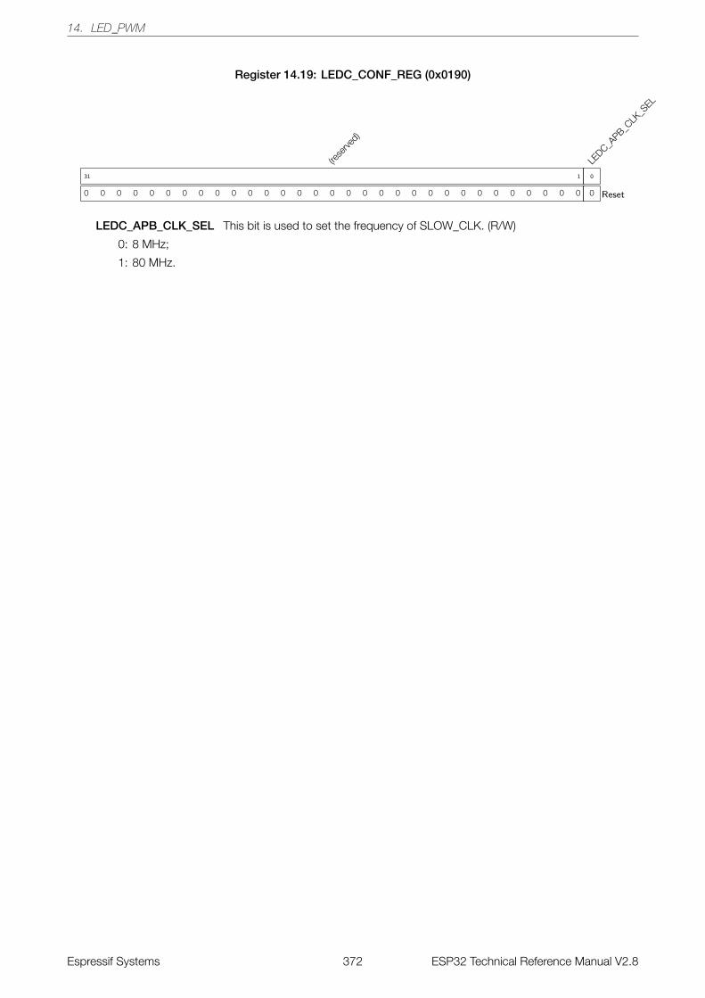
14. LED_PWM
Register 14.19: LEDC_CONF_REG (0x0190)
(rese
rved)
0 0 0 0 0 0 0 0 0 0 0 0 0 0 0 0 0 0 0 0 0 0 0 0 0 0 0 0 0 0 0
31 1
LEDC_A
PB_CLK
_SEL
0
0
Reset
LEDC_APB_CLK_SEL This bit is used to set the frequency of SLOW_CLK. (R/W)
0: 8 MHz;
1: 80 MHz.
Espressif Systems 372 ESP32 Technical Reference Manual V2.8
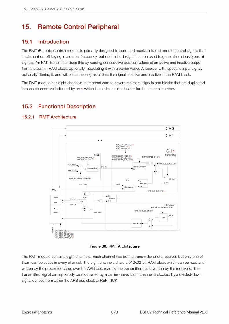
15. REMOTE CONTROL PERIPHERAL
15. Remote Control Peripheral
15.1 Introduction
The RMT (Remote Control) module is primarily designed to send and receive infrared remote control signals that
implement on-off keying in a carrier frequency, but due to its design it can be used to generate various types of
signals. An RMT transmitter does this by reading consecutive duration values of an active and inactive output
from the built-in RAM block, optionally modulating it with a carrier wave. A receiver will inspect its input signal,
optionally filtering it, and will place the lengths of time the signal is active and inactive in the RAM block.
The RMT module has eight channels, numbered zero to seven; registers, signals and blocks that are duplicated
in each channel are indicated by an n which is used as a placeholder for the channel number.
15.2 Functional Description
15.2.1 RMT Architecture
Figure 88: RMT Architecture
The RMT module contains eight channels. Each channel has both a transmitter and a receiver, but only one of
them can be active in every channel. The eight channels share a 512x32-bit RAM block which can be read and
written by the processor cores over the APB bus, read by the transmitters, and written by the receivers. The
transmitted signal can optionally be modulated by a carrier wave. Each channel is clocked by a divided-down
signal derived from either the APB bus clock or REF_TICK.
Espressif Systems 373 ESP32 Technical Reference Manual V2.8
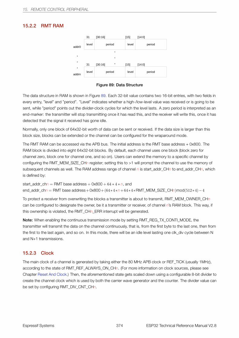
15. REMOTE CONTROL PERIPHERAL
15.2.2 RMT RAM
Figure 89: Data Structure
The data structure in RAM is shown in Figure 89. Each 32-bit value contains two 16-bit entries, with two fields in
every entry, ”level” and ”period”. ”Level” indicates whether a high-/low-level value was received or is going to be
sent, while ”period” points out the divider-clock cycles for which the level lasts. A zero period is interpreted as an
end-marker: the transmitter will stop transmitting once it has read this, and the receiver will write this, once it has
detected that the signal it received has gone idle.
Normally, only one block of 64x32-bit worth of data can be sent or received. If the data size is larger than this
block size, blocks can be extended or the channel can be configured for the wraparound mode.
The RMT RAM can be accessed via the APB bus. The initial address is the RMT base address + 0x800. The
RAM block is divided into eight 64x32-bit blocks. By default, each channel uses one block (block zero for
channel zero, block one for channel one, and so on). Users can extend the memory to a specific channel by
configuring the RMT_MEM_SIZE_CHn register; setting this to >1 will prompt the channel to use the memory of
subsequent channels as well. The RAM address range of channel n is start_addr_CHn to end_addr_CHn, which
is defined by:
start_addr_chn = RMT base address + 0x800 + 64 ∗ 4 ∗ n, and
end_addr_chn = RMT base address+0x800+(64∗4∗n+64∗4∗RMT_MEM_SIZE_CHn)mod(512∗4)−4
To protect a receiver from overwriting the blocks a transmitter is about to transmit, RMT_MEM_OWNER_CHn
can be configured to designate the owner, be it a transmitter or receiver, of channel n’s RAM block. This way, if
this ownership is violated, the RMT_CHn_ERR interrupt will be generated.
Note: When enabling the continuous transmission mode by setting RMT_REG_TX_CONTI_MODE, the
transmitter will transmit the data on the channel continuously, that is, from the first byte to the last one, then from
the first to the last again, and so on. In this mode, there will be an idle level lasting one clk_div cycle between N
and N+1 transmissions.
15.2.3 Clock
The main clock of a channel is generated by taking either the 80 MHz APB clock or REF_TICK (usually 1MHz),
according to the state of RMT_REF_ALWAYS_ON_CHn. (For more information on clock sources, please see
Chapter Reset And Clock.) Then, the aforementioned state gets scaled down using a configurable 8-bit divider to
create the channel clock which is used by both the carrier wave generator and the counter. The divider value can
be set by configuring RMT_DIV_CNT_CHn.
Espressif Systems 374 ESP32 Technical Reference Manual V2.8
15. REMOTE CONTROL PERIPHERAL
15.2.4 Transmitter
When the RMT_TX_START_CHn register is 1, the transmitter of channel n will start reading and sending data
from RAM. The transmitter will receive a 32-bit value each time it reads from RAM. Of these 32 bits, the low
16-bit entry is sent first and the high entry second.
To transmit more data than can be fitted in the channel’s RAM, the wraparound mode can be enabled. In this
mode, when the transmitter has reached the last entry in the channel’s memory, it will loop back to the first byte.
To use this mechanism for sending more data than can be fitted in the channel’s RAM, fill the RAM with the initial
events and set RMT_CHn_TX_LIM_REG to cause an RMT_CHn_TX_THR_EVENT_INT interrupt before the
wraparound happens. Then, when the interrupt happens, the already sent data should be replaced by
subsequent events, so that when the wraparound happens the transmitter will seamlessly continue sending the
new events.
With or without the wraparound mode enabled, transmission ends when an entry with zero length is
encountered. When this happens, the transmitter will generate an RMT_CHn_TX_END_INT interrupt and return
to the idle state. When a transmitter is in the idle state, the output level defaults to end-mark 0. Users can also
configure RMT_IDLE_OUT_EN_CHn and RMT_IDLE_OUT_LV_CHn to control the output level manually.
The output of the transmitter can be modulated using a carrier wave by setting RMT_CARRIER_EN_CHn. The
carrier frequency and duty cycle can be configured by adjusting the carrier’s high and low durations in
channel-clock cycles, in RMT_CARRIER_HIGH_CHn and RMT_CARRIER_HIGH_CHn.
15.2.5 Receiver
When RMT_RX_EN_CHn is set to 1, the receiver in channel n becomes active, measuring the duration between
input signal edges. These will be written as period/level value pairs to the channel RAM in the same fashion as
the transmitter sends them. Receiving ends, when the receiver detects no change in signal level for more than
RMT_IDLE_THRES_CHn channel clock ticks. The receiver will write a final entry with 0 period, generate an
RMT_CHn_RX_END_INT_RAW interrupt and return to the idle state.
The receiver has an input signal filter which can be configured using RMT_RX_FILTER_EN_CHn: The filter will
remove pulses with a length of less than RMT_RX_FILTER_THRES_CHn in APB clock periods.
When the RMT module is inactive, the RAM can be put into low-power mode by setting the RMT_MEM_PD
register to 1.
15.2.6 Interrupts
• RMT_CHn_TX_THR_EVENT_INT: Triggered when the amount of data the transmitter has sent matches the
value of RMT_CHn_TX_LIM_REG.
• RMT_CHn_TX_END_INT: Triggered when the transmitter has finished transmitting the signal.
• RMT_CHn_RX_END_INT: Triggered when the receiver has finished receiving a signal.
15.3 Register Summary
Name Description Address Access
Configuration registers
RMT_CH0CONF0_REG Channel 0 config register 0 0x3FF56020 R/W
Espressif Systems 375 ESP32 Technical Reference Manual V2.8
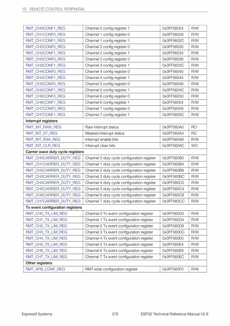
15. REMOTE CONTROL PERIPHERAL
RMT_CH0CONF1_REG Channel 0 config register 1 0x3FF56024 R/W
RMT_CH1CONF0_REG Channel 1 config register 0 0x3FF56028 R/W
RMT_CH1CONF1_REG Channel 1 config register 1 0x3FF5602C R/W
RMT_CH2CONF0_REG Channel 2 config register 0 0x3FF56030 R/W
RMT_CH2CONF1_REG Channel 2 config register 1 0x3FF56034 R/W
RMT_CH3CONF0_REG Channel 3 config register 0 0x3FF56038 R/W
RMT_CH3CONF1_REG Channel 3 config register 1 0x3FF5603C R/W
RMT_CH4CONF0_REG Channel 4 config register 0 0x3FF56040 R/W
RMT_CH4CONF1_REG Channel 4 config register 1 0x3FF56044 R/W
RMT_CH5CONF0_REG Channel 5 config register 0 0x3FF56048 R/W
RMT_CH5CONF1_REG Channel 5 config register 1 0x3FF5604C R/W
RMT_CH6CONF0_REG Channel 6 config register 0 0x3FF56050 R/W
RMT_CH6CONF1_REG Channel 6 config register 1 0x3FF56054 R/W
RMT_CH7CONF0_REG Channel 7 config register 0 0x3FF56058 R/W
RMT_CH7CONF1_REG Channel 7 config register 1 0x3FF5605C R/W
Interrupt registers
RMT_INT_RAW_REG Raw interrupt status 0x3FF560A0 RO
RMT_INT_ST_REG Masked interrupt status 0x3FF560A4 RO
RMT_INT_ENA_REG Interrupt enable bits 0x3FF560A8 R/W
RMT_INT_CLR_REG Interrupt clear bits 0x3FF560AC WO
Carrier wave duty cycle registers
RMT_CH0CARRIER_DUTY_REG Channel 0 duty cycle configuration register 0x3FF560B0 R/W
RMT_CH1CARRIER_DUTY_REG Channel 1 duty cycle configuration register 0x3FF560B4 R/W
RMT_CH2CARRIER_DUTY_REG Channel 2 duty cycle configuration register 0x3FF560B8 R/W
RMT_CH3CARRIER_DUTY_REG Channel 3 duty cycle configuration register 0x3FF560BC R/W
RMT_CH4CARRIER_DUTY_REG Channel 4 duty cycle configuration register 0x3FF560C0 R/W
RMT_CH5CARRIER_DUTY_REG Channel 5 duty cycle configuration register 0x3FF560C4 R/W
RMT_CH6CARRIER_DUTY_REG Channel 6 duty cycle configuration register 0x3FF560C8 R/W
RMT_CH7CARRIER_DUTY_REG Channel 7 duty cycle configuration register 0x3FF560CC R/W
Tx event configuration registers
RMT_CH0_TX_LIM_REG Channel 0 Tx event configuration register 0x3FF560D0 R/W
RMT_CH1_TX_LIM_REG Channel 1 Tx event configuration register 0x3FF560D4 R/W
RMT_CH2_TX_LIM_REG Channel 2 Tx event configuration register 0x3FF560D8 R/W
RMT_CH3_TX_LIM_REG Channel 3 Tx event configuration register 0x3FF560DC R/W
RMT_CH4_TX_LIM_REG Channel 4 Tx event configuration register 0x3FF560E0 R/W
RMT_CH5_TX_LIM_REG Channel 5 Tx event configuration register 0x3FF560E4 R/W
RMT_CH6_TX_LIM_REG Channel 6 Tx event configuration register 0x3FF560E8 R/W
RMT_CH7_TX_LIM_REG Channel 7 Tx event configuration register 0x3FF560EC R/W
Other registers
RMT_APB_CONF_REG RMT-wide configuration register 0x3FF560F0 R/W
Espressif Systems 376 ESP32 Technical Reference Manual V2.8
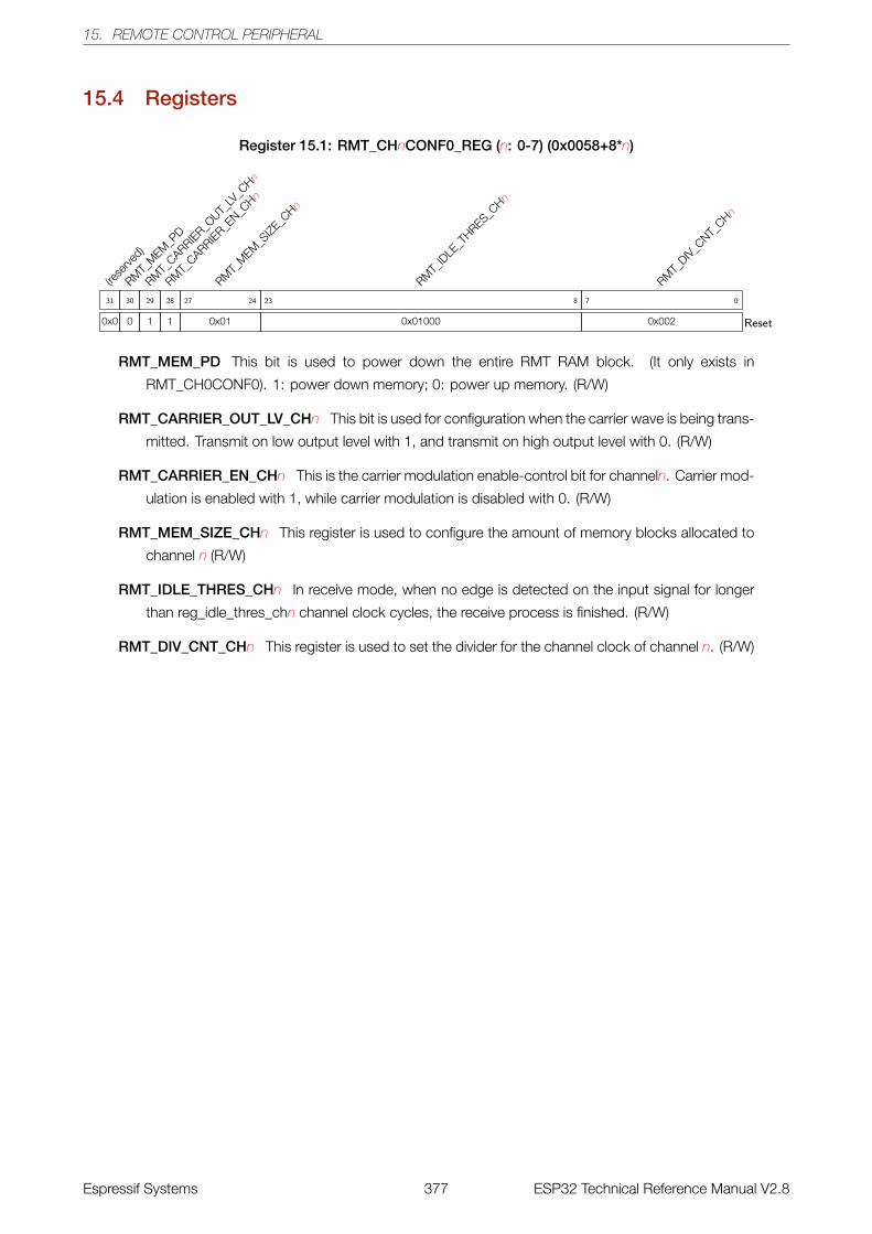
15. REMOTE CONTROL PERIPHERAL
15.4 Registers
Register 15.1: RMT_CHnCONF0_REG (n: 0-7) (0x0058+8*n)
(rese
rved)
0x0
31
RMT_
MEM
_PD
0
30
RMT_
CARRIER_OUT_
LV_C
Hn
1
29
RMT_
CARRIER_EN_C
Hn
1
28
RMT_
MEM
_SIZE
_CHn
0x01
27 24
RMT_
IDLE
_THRES_C
Hn
0x01000
23 8
RMT_
DIV_CNT_
CHn
0x002
7 0
Reset
RMT_MEM_PD This bit is used to power down the entire RMT RAM block. (It only exists in
RMT_CH0CONF0). 1: power down memory; 0: power up memory. (R/W)
RMT_CARRIER_OUT_LV_CHn This bit is used for configuration when the carrier wave is being trans-
mitted. Transmit on low output level with 1, and transmit on high output level with 0. (R/W)
RMT_CARRIER_EN_CHn This is the carrier modulation enable-control bit for channeln. Carrier mod-
ulation is enabled with 1, while carrier modulation is disabled with 0. (R/W)
RMT_MEM_SIZE_CHn This register is used to configure the amount of memory blocks allocated to
channel n (R/W)
RMT_IDLE_THRES_CHn In receive mode, when no edge is detected on the input signal for longer
than reg_idle_thres_chn channel clock cycles, the receive process is finished. (R/W)
RMT_DIV_CNT_CHn This register is used to set the divider for the channel clock of channel n. (R/W)
Espressif Systems 377 ESP32 Technical Reference Manual V2.8
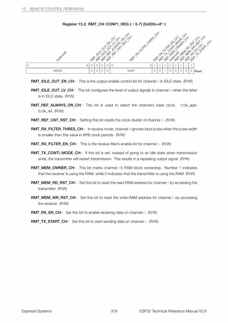
15. REMOTE CONTROL PERIPHERAL
Register 15.2: RMT_CHnCONF1_REG (n: 0-7) (0x005c+8*n)
(rese
rved)
0x0000
31 20
RMT_
IDLE
_OUT_
EN_CHn
0
19
RMT_
IDLE
_OUT_
LV_C
Hn
0
18
RMT_
REF_ALW
AYS_O
N_CHn
0
17
RMT_
REF_CNT_
RST_CHn
0
16
RMT_
RX_FIL
TER_T
HRES_CHn
0x00F
15 8
RMT_
RX_FIL
TER_E
N_CHn
0
7
RMT_
TX_C
ONTI_M
ODE_CHn
0
6
RMT_
MEM
_OW
NER_CHn
1
5
(rese
rved)
0
4
RMT_
MEM
_RD_R
ST_CHn
0
3
RMT_
MEM
_WR_R
ST_CHn
0
2
RMT_
RX_EN_C
Hn
0
1
RMT_
TX_S
TART_
CHn
0
0
Reset
RMT_IDLE_OUT_EN_CHn This is the output enable-control bit for channel n in IDLE state. (R/W)
RMT_IDLE_OUT_LV_CHn This bit configures the level of output signals in channel n when the latter
is in IDLE state. (R/W)
RMT_REF_ALWAYS_ON_CHn This bit is used to select the channel’s base clock. 1:clk_apb;
0:clk_ref. (R/W)
RMT_REF_CNT_RST_CHn Setting this bit resets the clock divider of channel n. (R/W)
RMT_RX_FILTER_THRES_CHn In receive mode, channel n ignores input pulse when the pulse width
is smaller than this value in APB clock periods. (R/W)
RMT_RX_FILTER_EN_CHn This is the receive filter’s enable-bit for channel n. (R/W)
RMT_TX_CONTI_MODE_CHn If this bit is set, instead of going to an idle state when transmission
ends, the transmitter will restart transmission. This results in a repeating output signal. (R/W)
RMT_MEM_OWNER_CHn This bit marks channel n’s RAM block ownership. Number 1 indicates
that the receiver is using the RAM, while 0 indicates that the transmitter is using the RAM. (R/W)
RMT_MEM_RD_RST_CHn Set this bit to reset the read-RAM address for channel n by accessing the
transmitter. (R/W)
RMT_MEM_WR_RST_CHn Set this bit to reset the write-RAM address for channel n by accessing
the receiver. (R/W)
RMT_RX_EN_CHn Set this bit to enable receiving data on channel n. (R/W)
RMT_TX_START_CHn Set this bit to start sending data on channel n. (R/W)
Espressif Systems 378 ESP32 Technical Reference Manual V2.8

15. REMOTE CONTROL PERIPHERAL
Register 15.3: RMT_INT_RAW_REG (0x00a0)
RMT_
CH7_TX
_THR_E
VENT_IN
T_RAW
0
31
RMT_
CH6_TX
_THR_E
VENT_IN
T_RAW
0
30
RMT_
CH5_TX
_THR_E
VENT_IN
T_RAW
0
29
RMT_
CH4_TX
_THR_E
VENT_IN
T_RAW
0
28
RMT_
CH3_TX
_THR_E
VENT_IN
T_RAW
0
27
RMT_
CH2_TX
_THR_E
VENT_IN
T_RAW
0
26
RMT_
CH1_TX
_THR_E
VENT_IN
T_RAW
0
25
RMT_
CH0_TX
_THR_E
VENT_IN
T_RAW
0
24
RMT_
CH7_ERR_IN
T_RAW
0
23
RMT_
CH7_RX_
END_INT_
RAW
0
22
RMT_
CH7_TX
_END_IN
T_RAW
0
21
RMT_
CH6_ERR_IN
T_RAW
0
20
RMT_
CH6_RX_
END_INT_
RAW
0
19
RMT_
CH6_TX
_END_IN
T_RAW
0
18
RMT_
CH5_ERR_IN
T_RAW
0
17
RMT_
CH5_RX_
END_INT_
RAW
0
16
RMT_
CH5_TX
_END_IN
T_RAW
0
15
RMT_
CH4_ERR_IN
T_RAW
0
14
RMT_
CH4_RX_
END_INT_
RAW
0
13
RMT_
CH4_TX
_END_IN
T_RAW
0
12
RMT_
CH3_ERR_IN
T_RAW
0
11
RMT_
CH3_RX_
END_INT_
RAW
0
10
RMT_
CH3_TX
_END_IN
T_RAW
0
9
RMT_
CH2_ERR_IN
T_RAW
0
8
RMT_
CH2_RX_
END_INT_
RAW
0
7
RMT_
CH2_TX
_END_IN
T_RAW
0
6
RMT_
CH1_ERR_IN
T_RAW
0
5
RMT_
CH1_RX_
END_INT_
RAW
0
4
RMT_
CH1_TX
_END_IN
T_RAW
0
3
RMT_
CH0_ERR_IN
T_RAW
0
2
RMT_
CH0_RX_
END_INT_
RAW
0
1
RMT_
CH0_TX
_END_IN
T_RAW
0
0
Reset
RMT_CHn_TX_THR_EVENT_INT_RAW The raw interrupt status bit for the
RMT_CHn_TX_THR_EVENT_INT interrupt. (RO)
RMT_CHn_ERR_INT_RAW The raw interrupt status bit for the RMT_CHn_ERR_INT interrupt. (RO)
RMT_CHn_RX_END_INT_RAW The raw interrupt status bit for the RMT_CHn_RX_END_INT inter-
rupt. (RO)
RMT_CHn_TX_END_INT_RAW The raw interrupt status bit for the RMT_CHn_TX_END_INT interrupt.
(RO)
Register 15.4: RMT_INT_ST_REG (0x00a4)
RMT_
CH7_TX
_THR_E
VENT_IN
T_ST
0
31
RMT_
CH6_TX
_THR_E
VENT_IN
T_ST
0
30
RMT_
CH5_TX
_THR_E
VENT_IN
T_ST
0
29
RMT_
CH4_TX
_THR_E
VENT_IN
T_ST
0
28
RMT_
CH3_TX
_THR_E
VENT_IN
T_ST
0
27
RMT_
CH2_TX
_THR_E
VENT_IN
T_ST
0
26
RMT_
CH1_TX
_THR_E
VENT_IN
T_ST
0
25
RMT_
CH0_TX
_THR_E
VENT_IN
T_ST
0
24
RMT_
CH7_ERR_IN
T_ST
0
23
RMT_
CH7_RX_
END_INT_
ST
0
22
RMT_
CH7_TX
_END_IN
T_ST
0
21
RMT_
CH6_ERR_IN
T_ST
0
20
RMT_
CH6_RX_
END_INT_
ST
0
19
RMT_
CH6_TX
_END_IN
T_ST
0
18
RMT_
CH5_ERR_IN
T_ST
0
17
RMT_
CH5_RX_
END_INT_
ST
0
16
RMT_
CH5_TX
_END_IN
T_ST
0
15
RMT_
CH4_ERR_IN
T_ST
0
14
RMT_
CH4_RX_
END_INT_
ST
0
13
RMT_
CH4_TX
_END_IN
T_ST
0
12
RMT_
CH3_ERR_IN
T_ST
0
11
RMT_
CH3_RX_
END_INT_
ST
0
10
RMT_
CH3_TX
_END_IN
T_ST
0
9
RMT_
CH2_ERR_IN
T_ST
0
8
RMT_
CH2_RX_
END_INT_
ST
0
7
RMT_
CH2_TX
_END_IN
T_ST
0
6
RMT_
CH1_ERR_IN
T_ST
0
5
RMT_
CH1_RX_
END_INT_
ST
0
4
RMT_
CH1_TX
_END_IN
T_ST
0
3
RMT_
CH0_ERR_IN
T_ST
0
2
RMT_
CH0_RX_
END_INT_
ST
0
1
RMT_
CH0_TX
_END_IN
T_ST
0
0
Reset
RMT_CHn_TX_THR_EVENT_INT_ST The masked interrupt status bit for the
RMT_CHn_TX_THR_EVENT_INT interrupt. (RO)
RMT_CHn_ERR_INT_ST The masked interrupt status bit for the RMT_CHn_ERR_INT interrupt. (RO)
RMT_CHn_RX_END_INT_ST The masked interrupt status bit for the RMT_CHn_RX_END_INT inter-
rupt. (RO)
RMT_CHn_TX_END_INT_ST The masked interrupt status bit for the RMT_CHn_TX_END_INT inter-
rupt. (RO)
Espressif Systems 379 ESP32 Technical Reference Manual V2.8
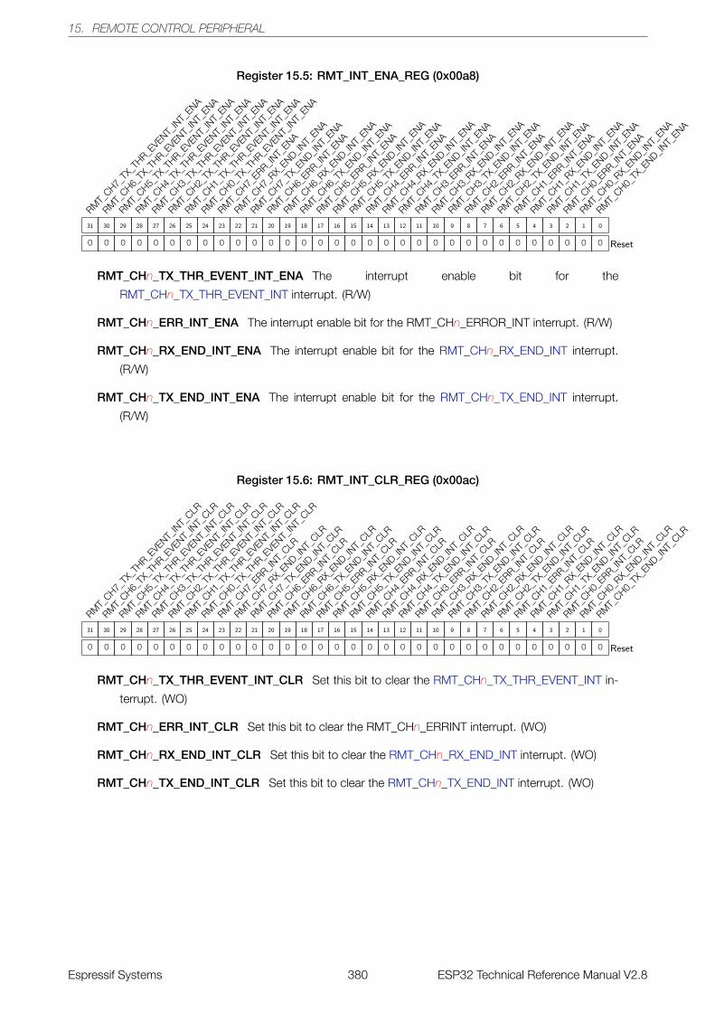
15. REMOTE CONTROL PERIPHERAL
Register 15.5: RMT_INT_ENA_REG (0x00a8)
RMT_
CH7_TX
_THR_E
VENT_IN
T_ENA
0
31
RMT_
CH6_TX
_THR_E
VENT_IN
T_ENA
0
30
RMT_
CH5_TX
_THR_E
VENT_IN
T_ENA
0
29
RMT_
CH4_TX
_THR_E
VENT_IN
T_ENA
0
28
RMT_
CH3_TX
_THR_E
VENT_IN
T_ENA
0
27
RMT_
CH2_TX
_THR_E
VENT_IN
T_ENA
0
26
RMT_
CH1_TX
_THR_E
VENT_IN
T_ENA
0
25
RMT_
CH0_TX
_THR_E
VENT_IN
T_ENA
0
24
RMT_
CH7_ERR_IN
T_ENA
0
23
RMT_
CH7_RX_
END_INT_
ENA
0
22
RMT_
CH7_TX
_END_IN
T_ENA
0
21
RMT_
CH6_ERR_IN
T_ENA
0
20
RMT_
CH6_RX_
END_INT_
ENA
0
19
RMT_
CH6_TX
_END_IN
T_ENA
0
18
RMT_
CH5_ERR_IN
T_ENA
0
17
RMT_
CH5_RX_
END_INT_
ENA
0
16
RMT_
CH5_TX
_END_IN
T_ENA
0
15
RMT_
CH4_ERR_IN
T_ENA
0
14
RMT_
CH4_RX_
END_INT_
ENA
0
13
RMT_
CH4_TX
_END_IN
T_ENA
0
12
RMT_
CH3_ERR_IN
T_ENA
0
11
RMT_
CH3_RX_
END_INT_
ENA
0
10
RMT_
CH3_TX
_END_IN
T_ENA
0
9
RMT_
CH2_ERR_IN
T_ENA
0
8
RMT_
CH2_RX_
END_INT_
ENA
0
7
RMT_
CH2_TX
_END_IN
T_ENA
0
6
RMT_
CH1_ERR_IN
T_ENA
0
5
RMT_
CH1_RX_
END_INT_
ENA
0
4
RMT_
CH1_TX
_END_IN
T_ENA
0
3
RMT_
CH0_ERR_IN
T_ENA
0
2
RMT_
CH0_RX_
END_INT_
ENA
0
1
RMT_
CH0_TX
_END_IN
T_ENA
0
0
Reset
RMT_CHn_TX_THR_EVENT_INT_ENA The interrupt enable bit for the
RMT_CHn_TX_THR_EVENT_INT interrupt. (R/W)
RMT_CHn_ERR_INT_ENA The interrupt enable bit for the RMT_CHn_ERROR_INT interrupt. (R/W)
RMT_CHn_RX_END_INT_ENA The interrupt enable bit for the RMT_CHn_RX_END_INT interrupt.
(R/W)
RMT_CHn_TX_END_INT_ENA The interrupt enable bit for the RMT_CHn_TX_END_INT interrupt.
(R/W)
Register 15.6: RMT_INT_CLR_REG (0x00ac)
RMT_
CH7_TX
_THR_E
VENT_IN
T_CLR
0
31
RMT_
CH6_TX
_THR_E
VENT_IN
T_CLR
0
30
RMT_
CH5_TX
_THR_E
VENT_IN
T_CLR
0
29
RMT_
CH4_TX
_THR_E
VENT_IN
T_CLR
0
28
RMT_
CH3_TX
_THR_E
VENT_IN
T_CLR
0
27
RMT_
CH2_TX
_THR_E
VENT_IN
T_CLR
0
26
RMT_
CH1_TX
_THR_E
VENT_IN
T_CLR
0
25
RMT_
CH0_TX
_THR_E
VENT_IN
T_CLR
0
24
RMT_
CH7_ERR_IN
T_CLR
0
23
RMT_
CH7_RX_
END_INT_
CLR
0
22
RMT_
CH7_TX
_END_IN
T_CLR
0
21
RMT_
CH6_ERR_IN
T_CLR
0
20
RMT_
CH6_RX_
END_INT_
CLR
0
19
RMT_
CH6_TX
_END_IN
T_CLR
0
18
RMT_
CH5_ERR_IN
T_CLR
0
17
RMT_
CH5_RX_
END_INT_
CLR
0
16
RMT_
CH5_TX
_END_IN
T_CLR
0
15
RMT_
CH4_ERR_IN
T_CLR
0
14
RMT_
CH4_RX_
END_INT_
CLR
0
13
RMT_
CH4_TX
_END_IN
T_CLR
0
12
RMT_
CH3_ERR_IN
T_CLR
0
11
RMT_
CH3_RX_
END_INT_
CLR
0
10
RMT_
CH3_TX
_END_IN
T_CLR
0
9
RMT_
CH2_ERR_IN
T_CLR
0
8
RMT_
CH2_RX_
END_INT_
CLR
0
7
RMT_
CH2_TX
_END_IN
T_CLR
0
6
RMT_
CH1_ERR_IN
T_CLR
0
5
RMT_
CH1_RX_
END_INT_
CLR
0
4
RMT_
CH1_TX
_END_IN
T_CLR
0
3
RMT_
CH0_ERR_IN
T_CLR
0
2
RMT_
CH0_RX_
END_INT_
CLR
0
1
RMT_
CH0_TX
_END_IN
T_CLR
0
0
Reset
RMT_CHn_TX_THR_EVENT_INT_CLR Set this bit to clear the RMT_CHn_TX_THR_EVENT_INT in-
terrupt. (WO)
RMT_CHn_ERR_INT_CLR Set this bit to clear the RMT_CHn_ERRINT interrupt. (WO)
RMT_CHn_RX_END_INT_CLR Set this bit to clear the RMT_CHn_RX_END_INT interrupt. (WO)
RMT_CHn_TX_END_INT_CLR Set this bit to clear the RMT_CHn_TX_END_INT interrupt. (WO)
Espressif Systems 380 ESP32 Technical Reference Manual V2.8
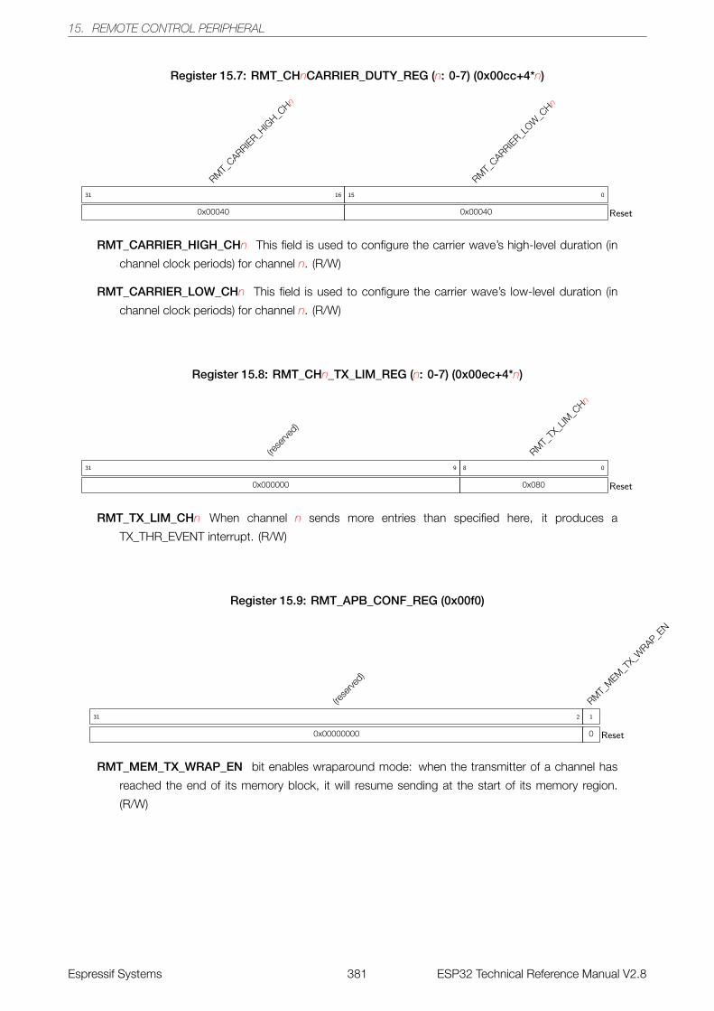
15. REMOTE CONTROL PERIPHERAL
Register 15.7: RMT_CHnCARRIER_DUTY_REG (n: 0-7) (0x00cc+4*n)
RMT_
CARRIER_HIG
H_CHn
0x00040
31 16
RMT_
CARRIER_LOW
_CHn
0x00040
15 0
Reset
RMT_CARRIER_HIGH_CHn This field is used to configure the carrier wave’s high-level duration (in
channel clock periods) for channel n. (R/W)
RMT_CARRIER_LOW_CHn This field is used to configure the carrier wave’s low-level duration (in
channel clock periods) for channel n. (R/W)
Register 15.8: RMT_CHn_TX_LIM_REG (n: 0-7) (0x00ec+4*n)
(rese
rved)
0x000000
31 9
RMT_
TX_L
IM_C
Hn
0x080
8 0
Reset
RMT_TX_LIM_CHn When channel n sends more entries than specified here, it produces a
TX_THR_EVENT interrupt. (R/W)
Register 15.9: RMT_APB_CONF_REG (0x00f0)
(rese
rved)
0x00000000
31 2
RMT_
MEM
_TX_
WRAP_E
N
0
1
Reset
RMT_MEM_TX_WRAP_EN bit enables wraparound mode: when the transmitter of a channel has
reached the end of its memory block, it will resume sending at the start of its memory region.
(R/W)
Espressif Systems 381 ESP32 Technical Reference Manual V2.8
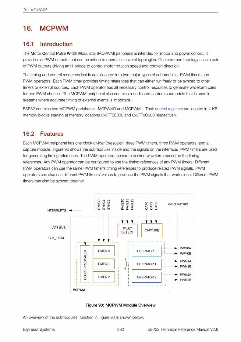
16. MCPWM
16. MCPWM
16.1 Introduction
The Motor Control Pulse Width Modulator (MCPWM) peripheral is intended for motor and power control. It
provides six PWM outputs that can be set up to operate in several topologies. One common topology uses a pair
of PWM outputs driving an H-bridge to control motor rotation speed and rotation direction.
The timing and control resources inside are allocated into two major types of submodules: PWM timers and
PWM operators. Each PWM timer provides timing references that can either run freely or be synced to other
timers or external sources. Each PWM operator has all necessary control resources to generate waveform pairs
for one PWM channel. The MCPWM peripheral also contains a dedicated capture submodule that is used in
systems where accurate timing of external events is important.
ESP32 contains two MCPWM peripherals: MCPWM0 and MCPWM1. Their control registers are located in 4-KB
memory blocks starting at memory locations 0x3FF5E000 and 0x3FF6C000 respectively.
16.2 Features
Each MCPWM peripheral has one clock divider (prescaler), three PWM timers, three PWM operators, and a
capture module. Figure 90 shows the submodules inside and the signals on the interface. PWM timers are used
for generating timing references. The PWM operators generate desired waveform based on the timing
references. Any PWM operator can be configured to use the timing references of any PWM timers. Different
PWM operators can use the same PWM timer’s timing references to produce related PWM signals. PWM
operators can also use different PWM timers’ values to produce the PWM signals that work alone. Different PWM
timers can also be synced together.
Figure 90: MCPWM Module Overview
An overview of the submodules’ function in Figure 90 is shown below:
Espressif Systems 382 ESP32 Technical Reference Manual V2.8
16. MCPWM
• PWM Timers 0, 1 and 2
– Every PWM timer has a dedicated 8-bit clock prescaler.
– The 16-bit counter in the PWM timer can work in count-up mode, count-down mode or
count-up-down mode.
– A hardware sync can trigger a reload on the PWM timer with a phase register. It will also trigger the
prescaler’ restart, so that the timer’s clock can also be synced. The source of the sync can come from
any GPIO or any other PWM timer’s sync_out.
• PWM Operators 0, 1 and 2
– Every PWM operator has two PWM outputs: PWMxA and PWMxB. They can work independently, in
symmetric and asymmetric configuration.
– Software, asynchronous override control of PWM signals.
– Configurable dead-time on rising and falling edges; each set up independently.
– All events can trigger CPU interrupts.
– Modulating of PWM output by high-frequency carrier signals, useful when gate drives are insulated
with a transformer.
– Period, time stamps and important control registers have shadow registers with flexible updating
methods.
• Fault Detection Module
– Programmable fault handling allocated on fault condition in both cycle-by-cycle mode and one-shot
mode.
– A fault condition can force the PWM output to either high or low logic levels.
• Capture Module
– Speed measurement of rotating machinery (for example, toothed sprockets sensed with Hall sensors)
– Measurement of elapsed time between position sensor pulses
– Period and duty-cycle measurement of pulse train signals
– Decoding current or voltage amplitude derived from duty-cycle-encoded signals from current/voltage
sensors
– Three individual capture channels, each of which has a time-stamp register (32 bits)
– Selection of edge polarity and prescaling of input capture signal
– The capture timer can sync with a PWM timer or external signals.
– Interrupt on each of the three capture channels
Espressif Systems 383 ESP32 Technical Reference Manual V2.8
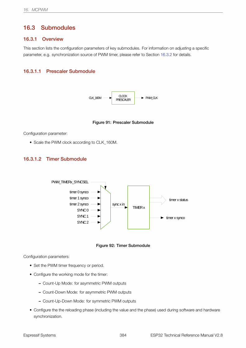
16. MCPWM
16.3 Submodules
16.3.1 Overview
This section lists the configuration parameters of key submodules. For information on adjusting a specific
parameter, e.g. synchronization source of PWM timer, please refer to Section 16.3.2 for details.
16.3.1.1 Prescaler Submodule
Figure 91: Prescaler Submodule
Configuration parameter:
• Scale the PWM clock according to CLK_160M.
16.3.1.2 Timer Submodule
Figure 92: Timer Submodule
Configuration parameters:
• Set the PWM timer frequency or period.
• Configure the working mode for the timer:
– Count-Up Mode: for asymmetric PWM outputs
– Count-Down Mode: for asymmetric PWM outputs
– Count-Up-Down Mode: for symmetric PWM outputs
• Configure the the reloading phase (including the value and the phase) used during software and hardware
synchronization.
Espressif Systems 384 ESP32 Technical Reference Manual V2.8
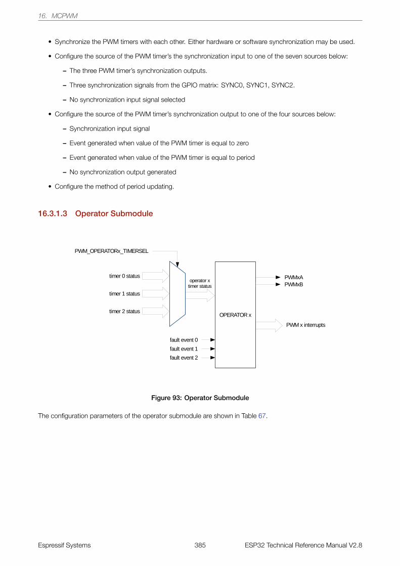
16. MCPWM
• Synchronize the PWM timers with each other. Either hardware or software synchronization may be used.
• Configure the source of the PWM timer’s the synchronization input to one of the seven sources below:
– The three PWM timer’s synchronization outputs.
– Three synchronization signals from the GPIO matrix: SYNC0, SYNC1, SYNC2.
– No synchronization input signal selected
• Configure the source of the PWM timer’s synchronization output to one of the four sources below:
– Synchronization input signal
– Event generated when value of the PWM timer is equal to zero
– Event generated when value of the PWM timer is equal to period
– No synchronization output generated
• Configure the method of period updating.
16.3.1.3 Operator Submodule
Figure 93: Operator Submodule
The configuration parameters of the operator submodule are shown in Table 67.
Espressif Systems 385 ESP32 Technical Reference Manual V2.8
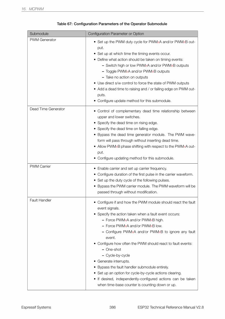
16. MCPWM
Table 67: Configuration Parameters of the Operator Submodule
Submodule Configuration Parameter or Option
PWM Generator • Set up the PWM duty cycle for PWMxA and/or PWMxB out-
put.
• Set up at which time the timing events occur.
• Define what action should be taken on timing events:
– Switch high or low PWMxA and/or PWMxB outputs
– Toggle PWMxA and/or PWMxB outputs
– Take no action on outputs
• Use direct s/w control to force the state of PWM outputs
• Add a dead time to raising and / or failing edge on PWM out-
puts.
• Configure update method for this submodule.
Dead Time Generator • Control of complementary dead time relationship between
upper and lower switches.
• Specify the dead time on rising edge.
• Specify the dead time on falling edge.
• Bypass the dead time generator module. The PWM wave-
form will pass through without inserting dead time.
• Allow PWMxB phase shifting with respect to the PWMxA out-
put.
• Configure updating method for this submodule.
PWM Carrier • Enable carrier and set up carrier frequency.
• Configure duration of the first pulse in the carrier waveform.
• Set up the duty cycle of the following pulses.
• Bypass the PWM carrier module. The PWM waveform will be
passed through without modification.
Fault Handler • Configure if and how the PWM module should react the fault
event signals.
• Specify the action taken when a fault event occurs:
– Force PWMxA and/or PWMxB high.
– Force PWMxA and/or PWMxB low.
– Configure PWMxA and/or PWMxB to ignore any fault
event.
• Configure how often the PWM should react to fault events:
– One-shot
– Cycle-by-cycle
• Generate interrupts.
• Bypass the fault handler submodule entirely.
• Set up an option for cycle-by-cycle actions clearing.
• If desired, independently-configured actions can be taken
when time-base counter is counting down or up.
Espressif Systems 386 ESP32 Technical Reference Manual V2.8
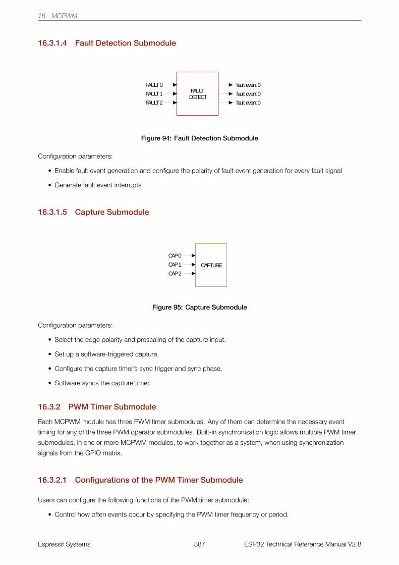
16. MCPWM
16.3.1.4 Fault Detection Submodule
Figure 94: Fault Detection Submodule
Configuration parameters:
• Enable fault event generation and configure the polarity of fault event generation for every fault signal
• Generate fault event interrupts
16.3.1.5 Capture Submodule
Figure 95: Capture Submodule
Configuration parameters:
• Select the edge polarity and prescaling of the capture input.
• Set up a software-triggered capture.
• Configure the capture timer’s sync trigger and sync phase.
• Software syncs the capture timer.
16.3.2 PWM Timer Submodule
Each MCPWM module has three PWM timer submodules. Any of them can determine the necessary event
timing for any of the three PWM operator submodules. Built-in synchronization logic allows multiple PWM timer
submodules, in one or more MCPWM modules, to work together as a system, when using synchronization
signals from the GPIO matrix.
16.3.2.1 Configurations of the PWM Timer Submodule
Users can configure the following functions of the PWM timer submodule:
• Control how often events occur by specifying the PWM timer frequency or period.
Espressif Systems 387 ESP32 Technical Reference Manual V2.8
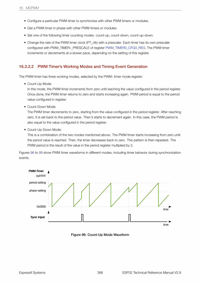
16. MCPWM
• Configure a particular PWM timer to synchronize with other PWM timers or modules.
• Get a PWM timer in phase with other PWM timers or modules.
• Set one of the following timer counting modes: count-up, count-down, count-up-down.
• Change the rate of the PWM timer clock (PT_clk) with a prescaler. Each timer has its own prescaler
configured with PWM_TIMERx_PRESCALE of register PWM_TIMER0_CFG0_REG. The PWM timer
increments or decrements at a slower pace, depending on the setting of this register.
16.3.2.2 PWM Timer’s Working Modes and Timing Event Generation
The PWM timer has three working modes, selected by the PWMx timer mode register:
• Count-Up Mode:
In this mode, the PWM timer increments from zero until reaching the value configured in the period register.
Once done, the PWM timer returns to zero and starts increasing again. PWM period is equal to the period
value configured in register.
• Count-Down Mode:
The PWM timer decrements to zero, starting from the value configured in the period register. After reaching
zero, it is set back to the period value. Then it starts to decrement again. In this case, the PWM period is
also equal to the value configured in the period register.
• Count-Up-Down Mode:
This is a combination of the two modes mentioned above. The PWM timer starts increasing from zero until
the period value is reached. Then, the timer decreases back to zero. This pattern is then repeated. The
PWM period is the result of the value in the period register multiplied by 2.
Figures 96 to 99 show PWM timer waveforms in different modes, including timer behavior during synchronization
events.
Figure 96: Count-Up Mode Waveform
Espressif Systems 388 ESP32 Technical Reference Manual V2.8
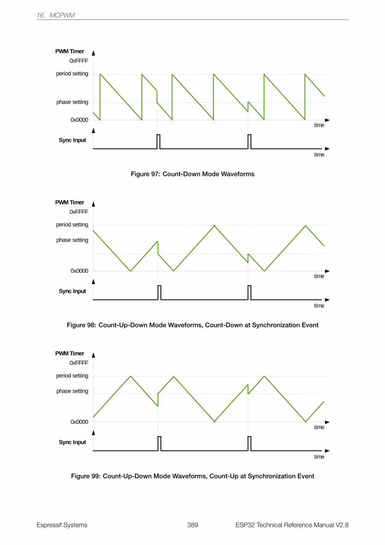
16. MCPWM
Figure 97: Count-Down Mode Waveforms
Figure 98: Count-Up-Down Mode Waveforms, Count-Down at Synchronization Event
Figure 99: Count-Up-Down Mode Waveforms, Count-Up at Synchronization Event
Espressif Systems 389 ESP32 Technical Reference Manual V2.8
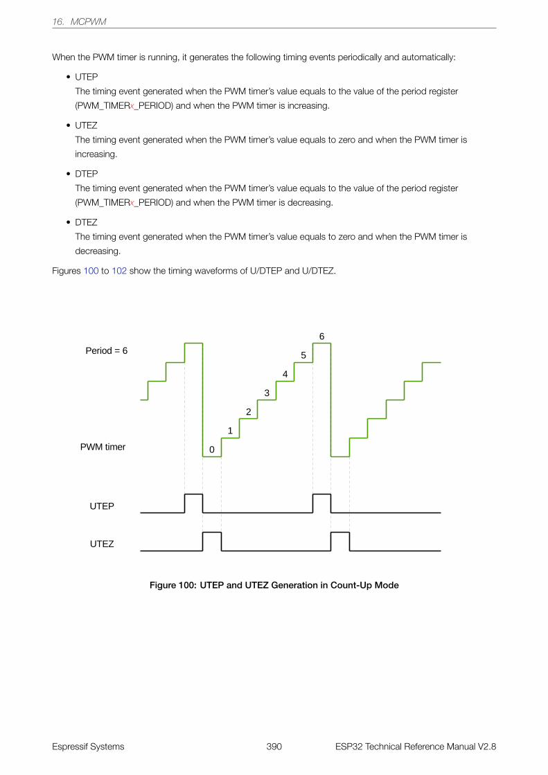
16. MCPWM
When the PWM timer is running, it generates the following timing events periodically and automatically:
• UTEP
The timing event generated when the PWM timer’s value equals to the value of the period register
(PWM_TIMERx_PERIOD) and when the PWM timer is increasing.
• UTEZ
The timing event generated when the PWM timer’s value equals to zero and when the PWM timer is
increasing.
• DTEP
The timing event generated when the PWM timer’s value equals to the value of the period register
(PWM_TIMERx_PERIOD) and when the PWM timer is decreasing.
• DTEZ
The timing event generated when the PWM timer’s value equals to zero and when the PWM timer is
decreasing.
Figures 100 to 102 show the timing waveforms of U/DTEP and U/DTEZ.
Figure 100: UTEP and UTEZ Generation in Count-Up Mode
Espressif Systems 390 ESP32 Technical Reference Manual V2.8
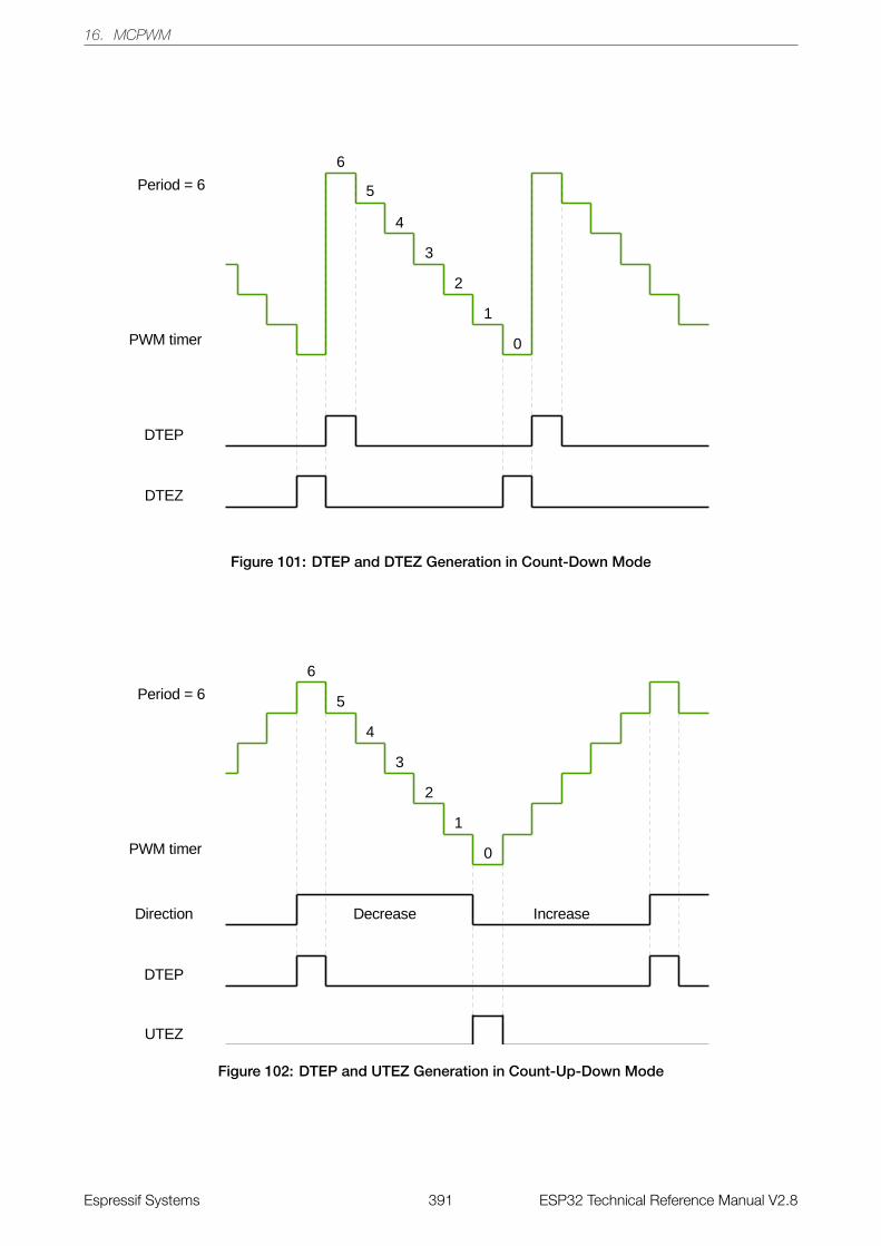
16. MCPWM
Figure 101: DTEP and DTEZ Generation in Count-Down Mode
Figure 102: DTEP and UTEZ Generation in Count-Up-Down Mode
Espressif Systems 391 ESP32 Technical Reference Manual V2.8
16. MCPWM
16.3.2.3 PWM Timer Shadow Register
The PWM timer’s period register and the PWM timer’s clock prescaler register have shadow registers. The
purpose of a shadow register is to save a copy of the value to be written into the active register at a specific
moment synchronized with the hardware. Both register types are defined as follows:
• Active Register
This register is directly responsible for controlling all actions performed by hardware.
• Shadow Register
It acts as a temporary buffer for a value to be written on the active register. Before this happens, the content
of the shadow register has no direct effect on the controlled hardware. At a specific, user-configured point
in time, the value saved in the shadow register is copied to the active register. This helps to prevent spurious
operation of the hardware, which may happen when a register is asynchronously modified by software.
Both the shadow register and the active register have the same memory address. The software always
writes into, or reads from the shadow register. The moment of updating the active register is determined by
its specific update method register. The update can start when the PWM timer is equal to zero, when the
PWM timer is equal to period,at a synchronization moment, or immediately. Software can trigger a globally
forced update which will prompt all registers in the module to be updated according to shadow registers.
16.3.2.4 PWM Timer Synchronization and Phase Locking
The PWM modules adopt a flexible synchronization method. Each PWM timer has a synchronization input and a
synchronization output. The synchronization input can be selected from three synchronization outputs and three
synchronization signals from the GPIO matrix. The synchronization output can be generated from the
synchronization input signal, or when the PWM timer’s value is equal to period or zero. Thus, the PWM timers
can be chained together with their phase locked. During synchronization, the PWM timer clock prescaler will
reset its counter in order to synchronize the PWM timer clock.
16.3.3 PWM Operator Submodule
The PWM Operator submodule has the following functions:
• Generates a PWM signal pair, based on timing references obtained from the corresponding PWM timer.
• Each signal out of the PWM signal pair includes a specific pattern of dead time.
• Superimposes a carrier on the PWM signal, if configured to do so.
• Handles response under fault conditions.
Figure 103 shows the block diagram of a PWM operator.
Espressif Systems 392 ESP32 Technical Reference Manual V2.8
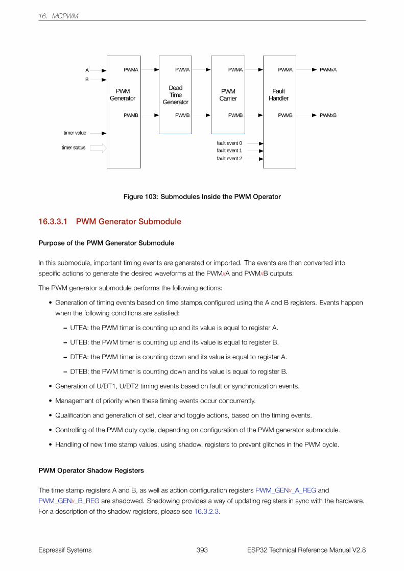
16. MCPWM
Figure 103: Submodules Inside the PWM Operator
16.3.3.1 PWM Generator Submodule
Purpose of the PWM Generator Submodule
In this submodule, important timing events are generated or imported. The events are then converted into
specific actions to generate the desired waveforms at the PWMxA and PWMxB outputs.
The PWM generator submodule performs the following actions:
• Generation of timing events based on time stamps configured using the A and B registers. Events happen
when the following conditions are satisfied:
– UTEA: the PWM timer is counting up and its value is equal to register A.
– UTEB: the PWM timer is counting up and its value is equal to register B.
– DTEA: the PWM timer is counting down and its value is equal to register A.
– DTEB: the PWM timer is counting down and its value is equal to register B.
• Generation of U/DT1, U/DT2 timing events based on fault or synchronization events.
• Management of priority when these timing events occur concurrently.
• Qualification and generation of set, clear and toggle actions, based on the timing events.
• Controlling of the PWM duty cycle, depending on configuration of the PWM generator submodule.
• Handling of new time stamp values, using shadow, registers to prevent glitches in the PWM cycle.
PWM Operator Shadow Registers
The time stamp registers A and B, as well as action configuration registers PWM_GENx_A_REG and
PWM_GENx_B_REG are shadowed. Shadowing provides a way of updating registers in sync with the hardware.
For a description of the shadow registers, please see 16.3.2.3.
Espressif Systems 393 ESP32 Technical Reference Manual V2.8
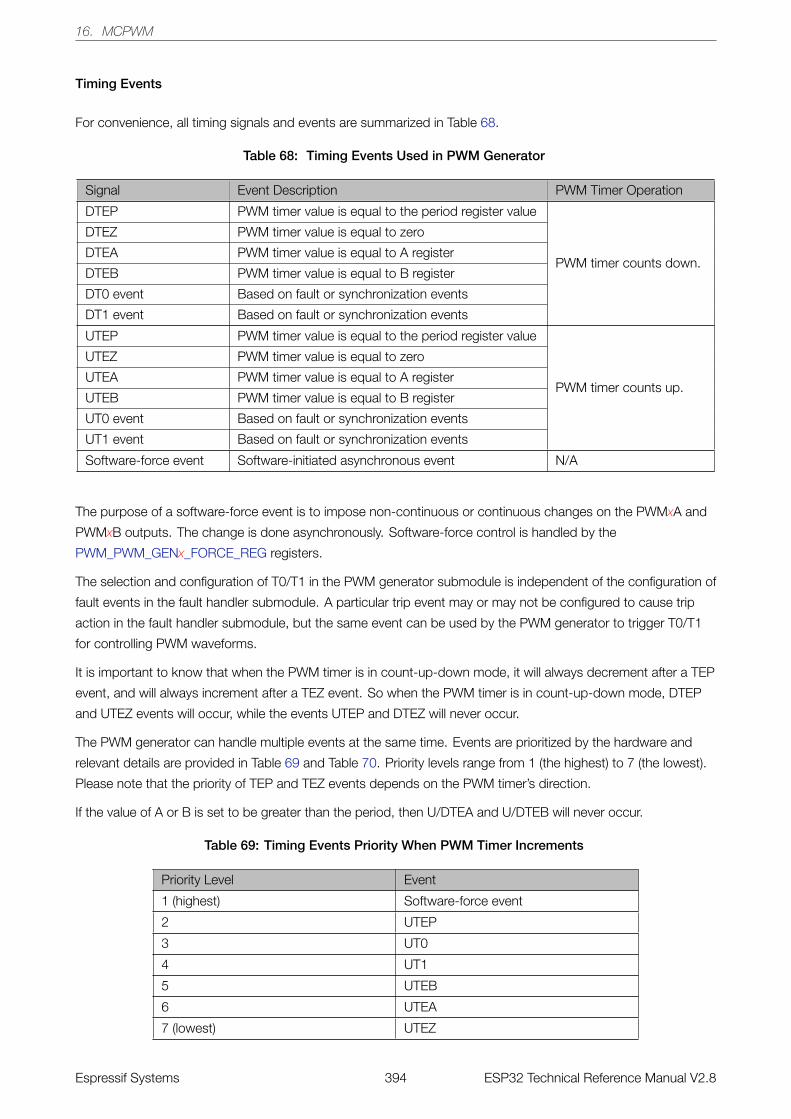
16. MCPWM
Timing Events
For convenience, all timing signals and events are summarized in Table 68.
Table 68: Timing Events Used in PWM Generator
Signal Event Description PWM Timer Operation
DTEP PWM timer value is equal to the period register value
PWM timer counts down.
DTEZ PWM timer value is equal to zero
DTEA PWM timer value is equal to A register
DTEB PWM timer value is equal to B register
DT0 event Based on fault or synchronization events
DT1 event Based on fault or synchronization events
UTEP PWM timer value is equal to the period register value
PWM timer counts up.
UTEZ PWM timer value is equal to zero
UTEA PWM timer value is equal to A register
UTEB PWM timer value is equal to B register
UT0 event Based on fault or synchronization events
UT1 event Based on fault or synchronization events
Software-force event Software-initiated asynchronous event N/A
The purpose of a software-force event is to impose non-continuous or continuous changes on the PWMxA and
PWMxB outputs. The change is done asynchronously. Software-force control is handled by the
PWM_PWM_GENx_FORCE_REG registers.
The selection and configuration of T0/T1 in the PWM generator submodule is independent of the configuration of
fault events in the fault handler submodule. A particular trip event may or may not be configured to cause trip
action in the fault handler submodule, but the same event can be used by the PWM generator to trigger T0/T1
for controlling PWM waveforms.
It is important to know that when the PWM timer is in count-up-down mode, it will always decrement after a TEP
event, and will always increment after a TEZ event. So when the PWM timer is in count-up-down mode, DTEP
and UTEZ events will occur, while the events UTEP and DTEZ will never occur.
The PWM generator can handle multiple events at the same time. Events are prioritized by the hardware and
relevant details are provided in Table 69 and Table 70. Priority levels range from 1 (the highest) to 7 (the lowest).
Please note that the priority of TEP and TEZ events depends on the PWM timer’s direction.
If the value of A or B is set to be greater than the period, then U/DTEA and U/DTEB will never occur.
Table 69: Timing Events Priority When PWM Timer Increments
Priority Level Event
1 (highest) Software-force event
2 UTEP
3 UT0
4 UT1
5 UTEB
6 UTEA
7 (lowest) UTEZ
Espressif Systems 394 ESP32 Technical Reference Manual V2.8
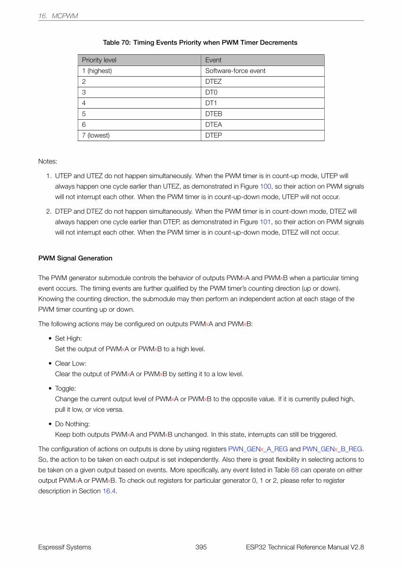
16. MCPWM
Table 70: Timing Events Priority when PWM Timer Decrements
Priority level Event
1 (highest) Software-force event
2 DTEZ
3 DT0
4 DT1
5 DTEB
6 DTEA
7 (lowest) DTEP
Notes:
1. UTEP and UTEZ do not happen simultaneously. When the PWM timer is in count-up mode, UTEP will
always happen one cycle earlier than UTEZ, as demonstrated in Figure 100, so their action on PWM signals
will not interrupt each other. When the PWM timer is in count-up-down mode, UTEP will not occur.
2. DTEP and DTEZ do not happen simultaneously. When the PWM timer is in count-down mode, DTEZ will
always happen one cycle earlier than DTEP, as demonstrated in Figure 101, so their action on PWM signals
will not interrupt each other. When the PWM timer is in count-up-down mode, DTEZ will not occur.
PWM Signal Generation
The PWM generator submodule controls the behavior of outputs PWMxA and PWMxB when a particular timing
event occurs. The timing events are further qualified by the PWM timer’s counting direction (up or down).
Knowing the counting direction, the submodule may then perform an independent action at each stage of the
PWM timer counting up or down.
The following actions may be configured on outputs PWMxA and PWMxB:
• Set High:
Set the output of PWMxA or PWMxB to a high level.
• Clear Low:
Clear the output of PWMxA or PWMxB by setting it to a low level.
• Toggle:
Change the current output level of PWMxA or PWMxB to the opposite value. If it is currently pulled high,
pull it low, or vice versa.
• Do Nothing:
Keep both outputs PWMxA and PWMxB unchanged. In this state, interrupts can still be triggered.
The configuration of actions on outputs is done by using registers PWN_GENx_A_REG and PWN_GENx_B_REG.
So, the action to be taken on each output is set independently. Also there is great flexibility in selecting actions to
be taken on a given output based on events. More specifically, any event listed in Table 68 can operate on either
output PWMxA or PWMxB. To check out registers for particular generator 0, 1 or 2, please refer to register
description in Section 16.4.
Espressif Systems 395 ESP32 Technical Reference Manual V2.8
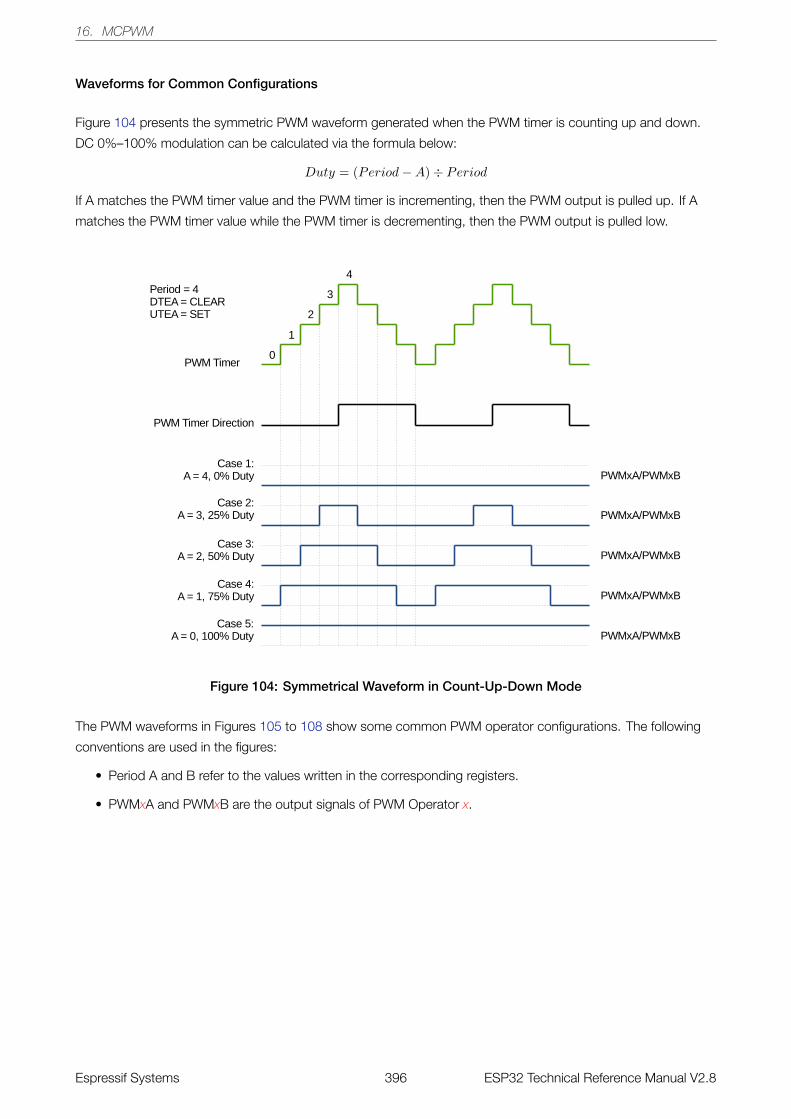
16. MCPWM
Waveforms for Common Configurations
Figure 104 presents the symmetric PWM waveform generated when the PWM timer is counting up and down.
DC 0%–100% modulation can be calculated via the formula below:
Duty = (Period−A)÷ Period
If A matches the PWM timer value and the PWM timer is incrementing, then the PWM output is pulled up. If A
matches the PWM timer value while the PWM timer is decrementing, then the PWM output is pulled low.
Figure 104: Symmetrical Waveform in Count-Up-Down Mode
The PWM waveforms in Figures 105 to 108 show some common PWM operator configurations. The following
conventions are used in the figures:
• Period A and B refer to the values written in the corresponding registers.
• PWMxA and PWMxB are the output signals of PWM Operator x.
Espressif Systems 396 ESP32 Technical Reference Manual V2.8
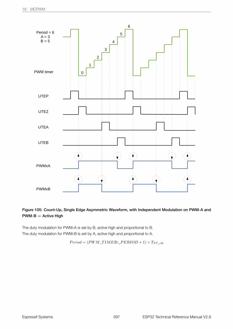
16. MCPWM
Figure 105: Count-Up, Single Edge Asymmetric Waveform, with Independent Modulation on PWMxA and
PWMxB — Active High
The duty modulation for PWMxA is set by B, active high and proportional to B.
The duty modulation for PWMxB is set by A, active high and proportional to A.
Period = (PWM_TIMERx_PERIOD + 1)× TPT _clk
Espressif Systems 397 ESP32 Technical Reference Manual V2.8
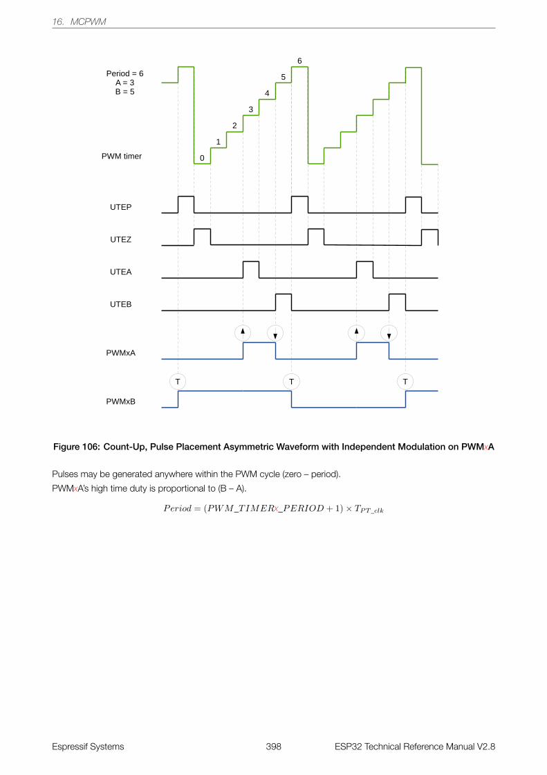
16. MCPWM
Figure 106: Count-Up, Pulse Placement Asymmetric Waveform with Independent Modulation on PWMxA
Pulses may be generated anywhere within the PWM cycle (zero – period).
PWMxA’s high time duty is proportional to (B – A).
Period = (PWM_TIMERx_PERIOD + 1)× TPT _clk
Espressif Systems 398 ESP32 Technical Reference Manual V2.8
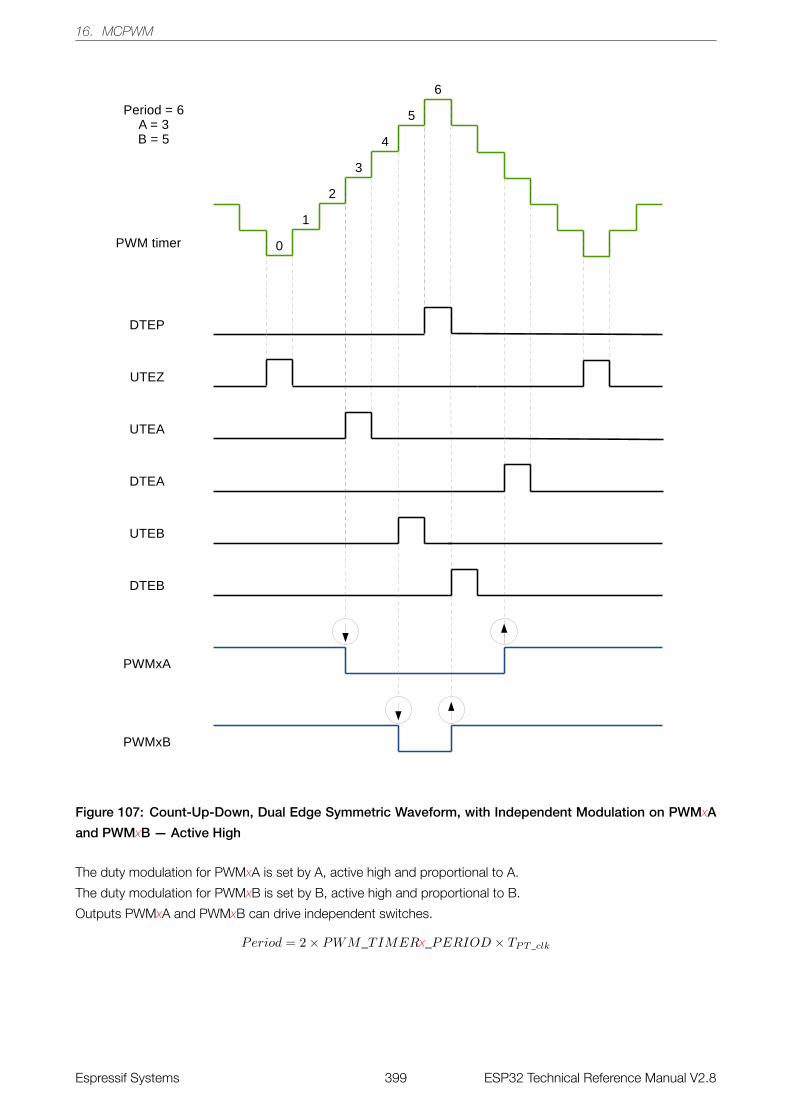
16. MCPWM
Figure 107: Count-Up-Down, Dual Edge Symmetric Waveform, with Independent Modulation on PWMxA
and PWMxB — Active High
The duty modulation for PWMxA is set by A, active high and proportional to A.
The duty modulation for PWMxB is set by B, active high and proportional to B.
Outputs PWMxA and PWMxB can drive independent switches.
Period = 2× PWM_TIMERx_PERIOD × TPT _clk
Espressif Systems 399 ESP32 Technical Reference Manual V2.8
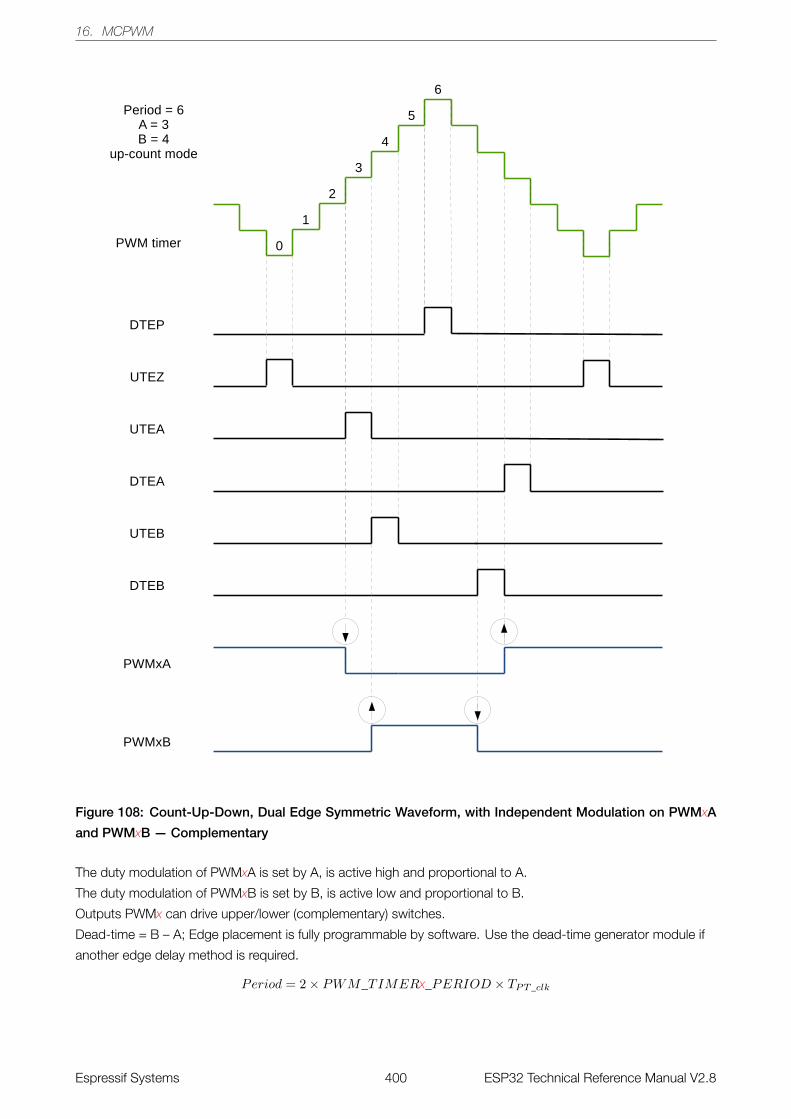
16. MCPWM
Figure 108: Count-Up-Down, Dual Edge Symmetric Waveform, with Independent Modulation on PWMxA
and PWMxB — Complementary
The duty modulation of PWMxA is set by A, is active high and proportional to A.
The duty modulation of PWMxB is set by B, is active low and proportional to B.
Outputs PWMx can drive upper/lower (complementary) switches.
Dead-time = B – A; Edge placement is fully programmable by software. Use the dead-time generator module if
another edge delay method is required.
Period = 2× PWM_TIMERx_PERIOD × TPT _clk
Espressif Systems 400 ESP32 Technical Reference Manual V2.8
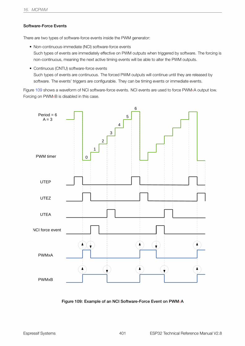
16. MCPWM
Software-Force Events
There are two types of software-force events inside the PWM generator:
• Non-continuous-immediate (NCI) software-force events
Such types of events are immediately effective on PWM outputs when triggered by software. The forcing is
non-continuous, meaning the next active timing events will be able to alter the PWM outputs.
• Continuous (CNTU) software-force events
Such types of events are continuous. The forced PWM outputs will continue until they are released by
software. The events’ triggers are configurable. They can be timing events or immediate events.
Figure 109 shows a waveform of NCI software-force events. NCI events are used to force PWMxA output low.
Forcing on PWMxB is disabled in this case.
Figure 109: Example of an NCI Software-Force Event on PWMxA
Espressif Systems 401 ESP32 Technical Reference Manual V2.8
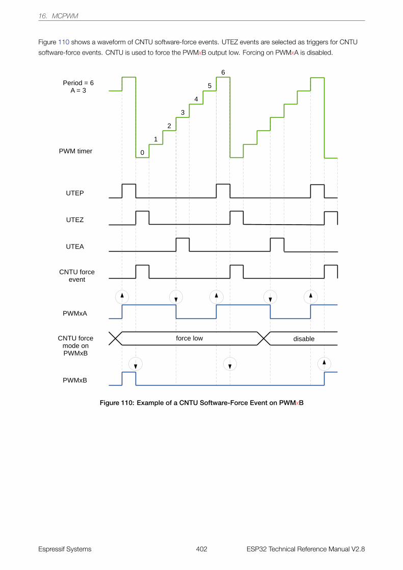
16. MCPWM
Figure 110 shows a waveform of CNTU software-force events. UTEZ events are selected as triggers for CNTU
software-force events. CNTU is used to force the PWMxB output low. Forcing on PWMxA is disabled.
Figure 110: Example of a CNTU Software-Force Event on PWMxB
Espressif Systems 402 ESP32 Technical Reference Manual V2.8
16. MCPWM
16.3.3.2 Dead Time Generator Submodule
Purpose of the Dead Time Generator Submodule
Several options to generate signals on PWMxA and PWMxB outputs, with a specific placement of signal edges,
have been discussed in section 16.3.3.1. The required dead time is obtained by altering the edge placement
between signals and by setting the signal’s duty cycle. Another option is to control the dead time using a
specialized submodule – the Dead Time Generator.
The key functions of the dead time generator submodule are as follows:
• Generating signal pairs (PWMxA and PWMxB) with a dead time from a single PWMxA input
• Creating a dead time by adding delay to signal edges:
– Rising edge delay (RED)
– Falling edge delay (FED)
• Configuring the signal pairs to be:
– Active high complementary (AHC)
– Active low complementary (ALC)
– Active high (AH)
– Active low (AL)
• This submodule may also be bypassed, if the dead time is configured directly in the generator submodule.
Dead Time Generator’s Shadow Registers
Delay registers RED and FED are shadowed with registers PWM_DTx_RED_CFG_REG and
PWM_DTx_FED_CFG_REG. For the description of shadow registers, please see section 16.3.2.3.
Espressif Systems 403 ESP32 Technical Reference Manual V2.8
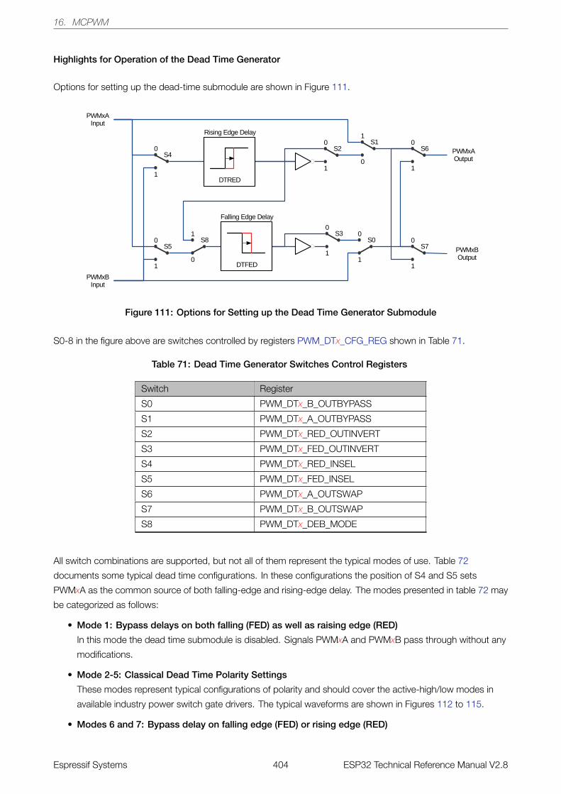
16. MCPWM
Highlights for Operation of the Dead Time Generator
Options for setting up the dead-time submodule are shown in Figure 111.
Figure 111: Options for Setting up the Dead Time Generator Submodule
S0-8 in the figure above are switches controlled by registers PWM_DTx_CFG_REG shown in Table 71.
Table 71: Dead Time Generator Switches Control Registers
Switch Register
S0 PWM_DTx_B_OUTBYPASS
S1 PWM_DTx_A_OUTBYPASS
S2 PWM_DTx_RED_OUTINVERT
S3 PWM_DTx_FED_OUTINVERT
S4 PWM_DTx_RED_INSEL
S5 PWM_DTx_FED_INSEL
S6 PWM_DTx_A_OUTSWAP
S7 PWM_DTx_B_OUTSWAP
S8 PWM_DTx_DEB_MODE
All switch combinations are supported, but not all of them represent the typical modes of use. Table 72
documents some typical dead time configurations. In these configurations the position of S4 and S5 sets
PWMxA as the common source of both falling-edge and rising-edge delay. The modes presented in table 72 may
be categorized as follows:
• Mode 1: Bypass delays on both falling (FED) as well as raising edge (RED)
In this mode the dead time submodule is disabled. Signals PWMxA and PWMxB pass through without any
modifications.
• Mode 2-5: Classical Dead Time Polarity Settings
These modes represent typical configurations of polarity and should cover the active-high/low modes in
available industry power switch gate drivers. The typical waveforms are shown in Figures 112 to 115.
• Modes 6 and 7: Bypass delay on falling edge (FED) or rising edge (RED)
Espressif Systems 404 ESP32 Technical Reference Manual V2.8

16. MCPWM
In these modes, either RED (Rising Edge Delay) or FED (Falling Edge Delay) is bypassed. As a result, the
corresponding delay is not applied.
Table 72: Typical Dead Time Generator Operating Modes
Mode Mode Description S0 S1 S2 S3
1 PWMxA and PWMxB Pass Through/No Delay 1 1 X X
2 Active High Complementary (AHC), see Figure 112 0 0 0 1
3 Active Low Complementary (ALC), see Figure 113 0 0 1 0
4 Active High (AH), see Figure 114 0 0 0 0
5 Active Low (AL), see Figure 115 0 0 1 1
6 PWMxA Output = PWMxA In (No Delay) 0 1 0 or 1 0 or 1
PWMxB Output = PWMxA Input with Falling Edge Delay
7 PWMxA Output = PWMxA Input with Rising Edge Delay 1 0 0 or 1 0 or 1
PWMxB Output = PWMxB Input with No Delay
Note: For all the modes above, the position of the binary switches S4 to S8 is set to 0.
Figure 112: Active High Complementary (AHC) Dead Time Waveforms
Rising edge (RED) and falling edge (FED) delays may be set up independently. The delay value is programmed
using the 16-bit registers PWM_DTx_RED and PWM_DTx_FED. The register value represents the number of
clock (DT_clk) periods by which a signal edge is delayed. DT_CLK can be selected from PWM_clk or PT_clk
through register PWM_DTx_CLK_SEL.
To calculate the delay on falling edge (FED) and rising edge (RED), use the following formulas:
FED = PWM_DT x_FED × TDT _clk
RED = PWM_DT x_RED × TDT _clk
Espressif Systems 405 ESP32 Technical Reference Manual V2.8
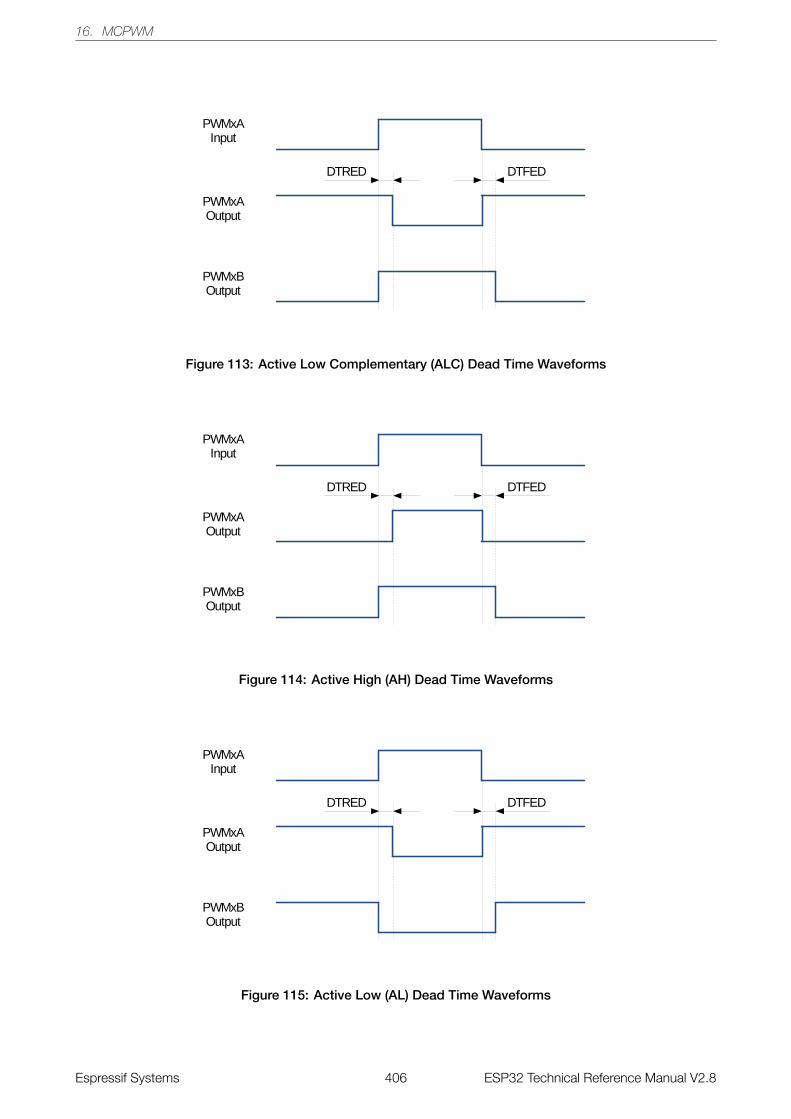
16. MCPWM
Figure 113: Active Low Complementary (ALC) Dead Time Waveforms
Figure 114: Active High (AH) Dead Time Waveforms
Figure 115: Active Low (AL) Dead Time Waveforms
Espressif Systems 406 ESP32 Technical Reference Manual V2.8
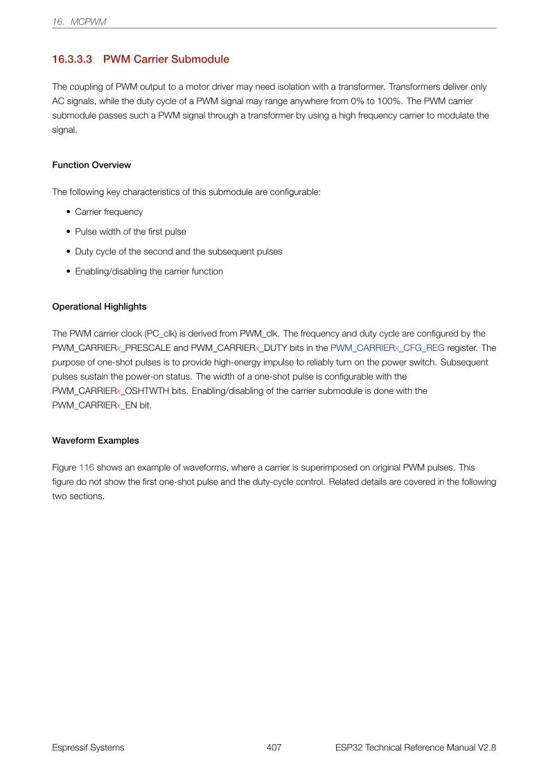
16. MCPWM
16.3.3.3 PWM Carrier Submodule
The coupling of PWM output to a motor driver may need isolation with a transformer. Transformers deliver only
AC signals, while the duty cycle of a PWM signal may range anywhere from 0% to 100%. The PWM carrier
submodule passes such a PWM signal through a transformer by using a high frequency carrier to modulate the
signal.
Function Overview
The following key characteristics of this submodule are configurable:
• Carrier frequency
• Pulse width of the first pulse
• Duty cycle of the second and the subsequent pulses
• Enabling/disabling the carrier function
Operational Highlights
The PWM carrier clock (PC_clk) is derived from PWM_clk. The frequency and duty cycle are configured by the
PWM_CARRIERx_PRESCALE and PWM_CARRIERx_DUTY bits in the PWM_CARRIERx_CFG_REG register. The
purpose of one-shot pulses is to provide high-energy impulse to reliably turn on the power switch. Subsequent
pulses sustain the power-on status. The width of a one-shot pulse is configurable with the
PWM_CARRIERx_OSHTWTH bits. Enabling/disabling of the carrier submodule is done with the
PWM_CARRIERx_EN bit.
Waveform Examples
Figure 116 shows an example of waveforms, where a carrier is superimposed on original PWM pulses. This
figure do not show the first one-shot pulse and the duty-cycle control. Related details are covered in the following
two sections.
Espressif Systems 407 ESP32 Technical Reference Manual V2.8
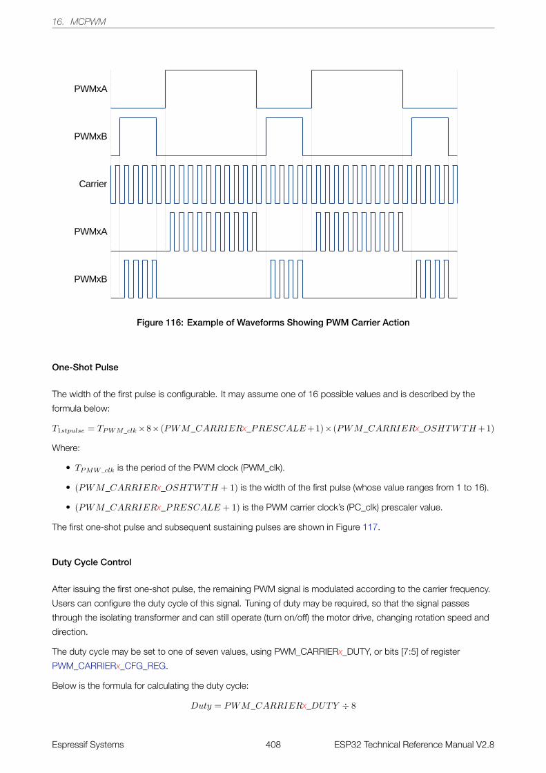
16. MCPWM
Figure 116: Example of Waveforms Showing PWM Carrier Action
One-Shot Pulse
The width of the first pulse is configurable. It may assume one of 16 possible values and is described by the
formula below:
T1stpulse = TPWM_clk×8× (PWM_CARRIERx_PRESCALE+1)× (PWM_CARRIERx_OSHTWTH+1)
Where:
• TPMW _clk is the period of the PWM clock (PWM_clk).
• (PWM_CARRIERx_OSHTWTH + 1) is the width of the first pulse (whose value ranges from 1 to 16).
• (PWM_CARRIERx_PRESCALE + 1) is the PWM carrier clock’s (PC_clk) prescaler value.
The first one-shot pulse and subsequent sustaining pulses are shown in Figure 117.
Duty Cycle Control
After issuing the first one-shot pulse, the remaining PWM signal is modulated according to the carrier frequency.
Users can configure the duty cycle of this signal. Tuning of duty may be required, so that the signal passes
through the isolating transformer and can still operate (turn on/off) the motor drive, changing rotation speed and
direction.
The duty cycle may be set to one of seven values, using PWM_CARRIERx_DUTY, or bits [7:5] of register
PWM_CARRIERx_CFG_REG.
Below is the formula for calculating the duty cycle:
Duty = PWM_CARRIERx_DUTY ÷ 8
Espressif Systems 408 ESP32 Technical Reference Manual V2.8
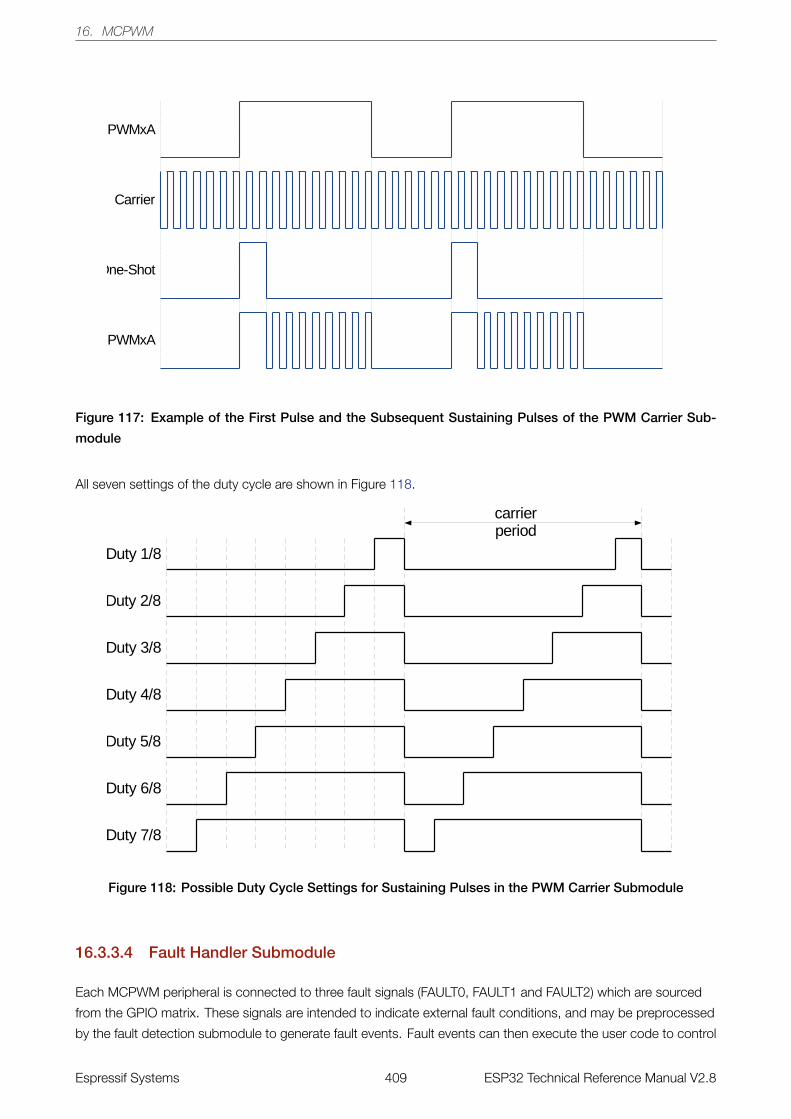
16. MCPWM
Figure 117: Example of the First Pulse and the Subsequent Sustaining Pulses of the PWM Carrier Sub-
module
All seven settings of the duty cycle are shown in Figure 118.
Figure 118: Possible Duty Cycle Settings for Sustaining Pulses in the PWM Carrier Submodule
16.3.3.4 Fault Handler Submodule
Each MCPWM peripheral is connected to three fault signals (FAULT0, FAULT1 and FAULT2) which are sourced
from the GPIO matrix. These signals are intended to indicate external fault conditions, and may be preprocessed
by the fault detection submodule to generate fault events. Fault events can then execute the user code to control
Espressif Systems 409 ESP32 Technical Reference Manual V2.8
16. MCPWM
MCPWM outputs in response to specific faults.
Function of Fault Handler Submodule
The key actions performed by the fault handler submodule are:
• Forcing outputs PWMxA and PWMxB, upon detected fault, to one of the following states:
– High
– Low
– Toggle
– No action taken
• Execution of one-shot trip (OST) upon detection of over-current conditions/short circuits.
• Cycle-by-cycle tripping (CBC) to provide current-limiting operation.
• Allocation of either one-shot or cycle-by-cycle operation for each fault signal.
• Generation of interrupts for each fault input.
• Support for software-force tripping.
• Enabling or disabling of submodule function as required.
Operation and Configuration Tips
This section provides the operational tips and set-up options for the fault handler submodule.
Fault signals coming from pads are sampled and synced in the GPIO matrix. In order to guarantee the successful
sampling of fault pulses, each pulse duration must be at least two APB clock cycles. The fault detection
submodule will then sample fault signals by using PWM_clk. So, the duration of fault pulses coming from GPIO
matrix must be at least one PWM_clk cycle. Differently put, regardless of the period relation between APB clock
and PWM_clk, the width of fault signal pulses on pads must be at least equal to the sum of two APB clock cycles
and one PWM_clk cycle.
Each level of fault signals, FAULT0 to FAULT2, can be used by the fault handler submodule to generate fault
events (fault_event0 to fault_event2). Every fault event can be configured individually to provide CBC action, OST
action, or none.
• Cycle-by-Cycle (CBC) action:
When CBC action is triggered, the state of PWMxA and PWMxB will be changed immediately according to
the configuration of registers PWM_FHx_A_CBC_U/D and PWM_FHx_B_CBC_U/D. Different actions can
be indicted when the PWM timer is incrementing or decrementing. Different CBC action interrupts can be
triggered for different fault events. Status register PWM_FHx_CBC_ON indicates whether a CBC action is
on or off. When the fault event is no longer present, CBC actions on PWMxA/B will be cleared at a
specified point, which is either a D/UTEP or D/UTEZ event. Register PWM_FHx_CBCPULSE determines at
which event PWMxA and PWMxB will be able to resume normal actions. Therefore, in this mode, the CBC
action is cleared or refreshed upon every PWM cycle.
• One-Shot (OST) action:
Espressif Systems 410 ESP32 Technical Reference Manual V2.8
16. MCPWM
When OST action is triggered, the state of PWMxA and PWMxB will be changed immediately, depending
on the setting of registers PWM_FHx_A_OST_U/D and PWM_FHx_B_OST_U/D. Different actions can be
configured when PWM timer is incrementing or decrementing. Different OST action interrupts can be
triggered form different fault events. Status register PWM_FHx_OST_ON indicates whether an OST action
is on or off. The OST actions on PWMxA/B are not automatically cleared when the fault event is no longer
present. One-shot actions must be cleared manually by negating the value stored in register
PWM_FHx_CLR_OST.
16.3.4 Capture Submodule
16.3.4.1 Introduction
The capture submodule contains three complete capture channels. Channel inputs CAP0, CAP1 and CAP2 are
sourced from the GPIO matrix. Thanks to the flexibility of the GPIO matrix, CAP0, CAP1 and CAP2 can be
configured from any PAD input. Multiple capture channels can be sourced from the same PAD input, while
prescaling for each channel can be set differently. Also, capture channels are sourced from different PADs. This
provides several options for handling capture signals by hardware in the background, instead of having them
processed directly by the CPU. A capture submodule has the following independent key resources:
• One 32-bit timer (counter) which can be synchronized with the PWM timer, another submodule or software.
• Three capture channels, each equipped with a 32-bit time-stamp and a capture prescaler.
• Independent edge polarity (rising/falling edge) selection for any capture channel.
• Input capture signal prescaling (from 1 to 256).
• Interrupt capabilities on any of the three capture events.
16.3.4.2 Capture Timer
The capture timer is a 32-bit counter incrementing continuously, once enabled. On the input it has an APB clock
running typically at 80 MHz. At a sync event the counter is loaded with phase stored in register
PWM_CAP_TIMER_PHASE_REG. Sync events can come from PWM timers sync-out, PWM module sync-in or
software. The capture timer provides timing references for all three capture channels.
16.3.4.3 Capture Channel
The capture signal coming to a capture channel will be inverted first, if needed, and then prescaled. Finally,
specified edges of preprocessed capture signal will trigger capture events. When a capture event occurs, the
capture timer’s value is stored in time-stamp register PWM_CAP_CHx_REG. Different interrupts can be
generated for different capture channels at capture events. The edge that triggers a capture event is recorded in
register PWM_CAPx_EDGE. The capture event can be also forced by software.
Espressif Systems 411 ESP32 Technical Reference Manual V2.8
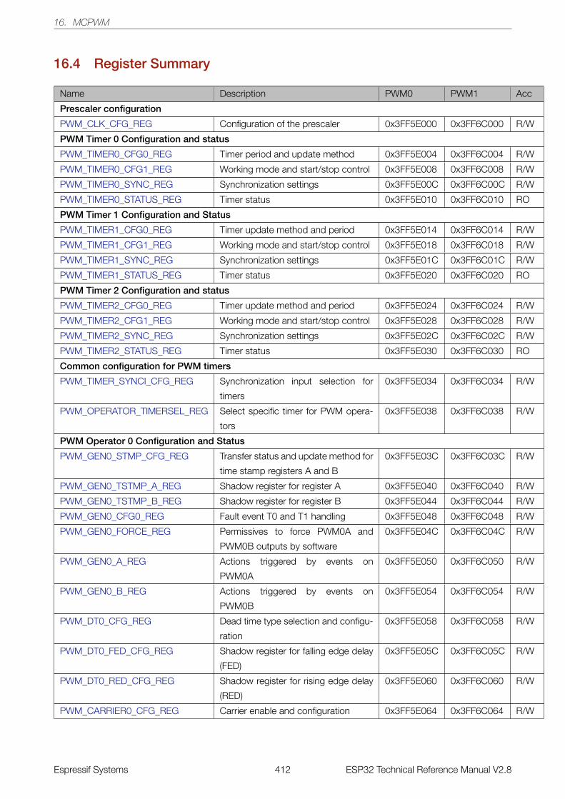
16. MCPWM
16.4 Register Summary
Name Description PWM0 PWM1 Acc
Prescaler configuration
PWM_CLK_CFG_REG Configuration of the prescaler 0x3FF5E000 0x3FF6C000 R/W
PWM Timer 0 Configuration and status
PWM_TIMER0_CFG0_REG Timer period and update method 0x3FF5E004 0x3FF6C004 R/W
PWM_TIMER0_CFG1_REG Working mode and start/stop control 0x3FF5E008 0x3FF6C008 R/W
PWM_TIMER0_SYNC_REG Synchronization settings 0x3FF5E00C 0x3FF6C00C R/W
PWM_TIMER0_STATUS_REG Timer status 0x3FF5E010 0x3FF6C010 RO
PWM Timer 1 Configuration and Status
PWM_TIMER1_CFG0_REG Timer update method and period 0x3FF5E014 0x3FF6C014 R/W
PWM_TIMER1_CFG1_REG Working mode and start/stop control 0x3FF5E018 0x3FF6C018 R/W
PWM_TIMER1_SYNC_REG Synchronization settings 0x3FF5E01C 0x3FF6C01C R/W
PWM_TIMER1_STATUS_REG Timer status 0x3FF5E020 0x3FF6C020 RO
PWM Timer 2 Configuration and status
PWM_TIMER2_CFG0_REG Timer update method and period 0x3FF5E024 0x3FF6C024 R/W
PWM_TIMER2_CFG1_REG Working mode and start/stop control 0x3FF5E028 0x3FF6C028 R/W
PWM_TIMER2_SYNC_REG Synchronization settings 0x3FF5E02C 0x3FF6C02C R/W
PWM_TIMER2_STATUS_REG Timer status 0x3FF5E030 0x3FF6C030 RO
Common configuration for PWM timers
PWM_TIMER_SYNCI_CFG_REG Synchronization input selection for
timers
0x3FF5E034 0x3FF6C034 R/W
PWM_OPERATOR_TIMERSEL_REG Select specific timer for PWM opera-
tors
0x3FF5E038 0x3FF6C038 R/W
PWM Operator 0 Configuration and Status
PWM_GEN0_STMP_CFG_REG Transfer status and update method for
time stamp registers A and B
0x3FF5E03C 0x3FF6C03C R/W
PWM_GEN0_TSTMP_A_REG Shadow register for register A 0x3FF5E040 0x3FF6C040 R/W
PWM_GEN0_TSTMP_B_REG Shadow register for register B 0x3FF5E044 0x3FF6C044 R/W
PWM_GEN0_CFG0_REG Fault event T0 and T1 handling 0x3FF5E048 0x3FF6C048 R/W
PWM_GEN0_FORCE_REG Permissives to force PWM0A and
PWM0B outputs by software
0x3FF5E04C 0x3FF6C04C R/W
PWM_GEN0_A_REG Actions triggered by events on
PWM0A
0x3FF5E050 0x3FF6C050 R/W
PWM_GEN0_B_REG Actions triggered by events on
PWM0B
0x3FF5E054 0x3FF6C054 R/W
PWM_DT0_CFG_REG Dead time type selection and configu-
ration
0x3FF5E058 0x3FF6C058 R/W
PWM_DT0_FED_CFG_REG Shadow register for falling edge delay
(FED)
0x3FF5E05C 0x3FF6C05C R/W
PWM_DT0_RED_CFG_REG Shadow register for rising edge delay
(RED)
0x3FF5E060 0x3FF6C060 R/W
PWM_CARRIER0_CFG_REG Carrier enable and configuration 0x3FF5E064 0x3FF6C064 R/W
Espressif Systems 412 ESP32 Technical Reference Manual V2.8
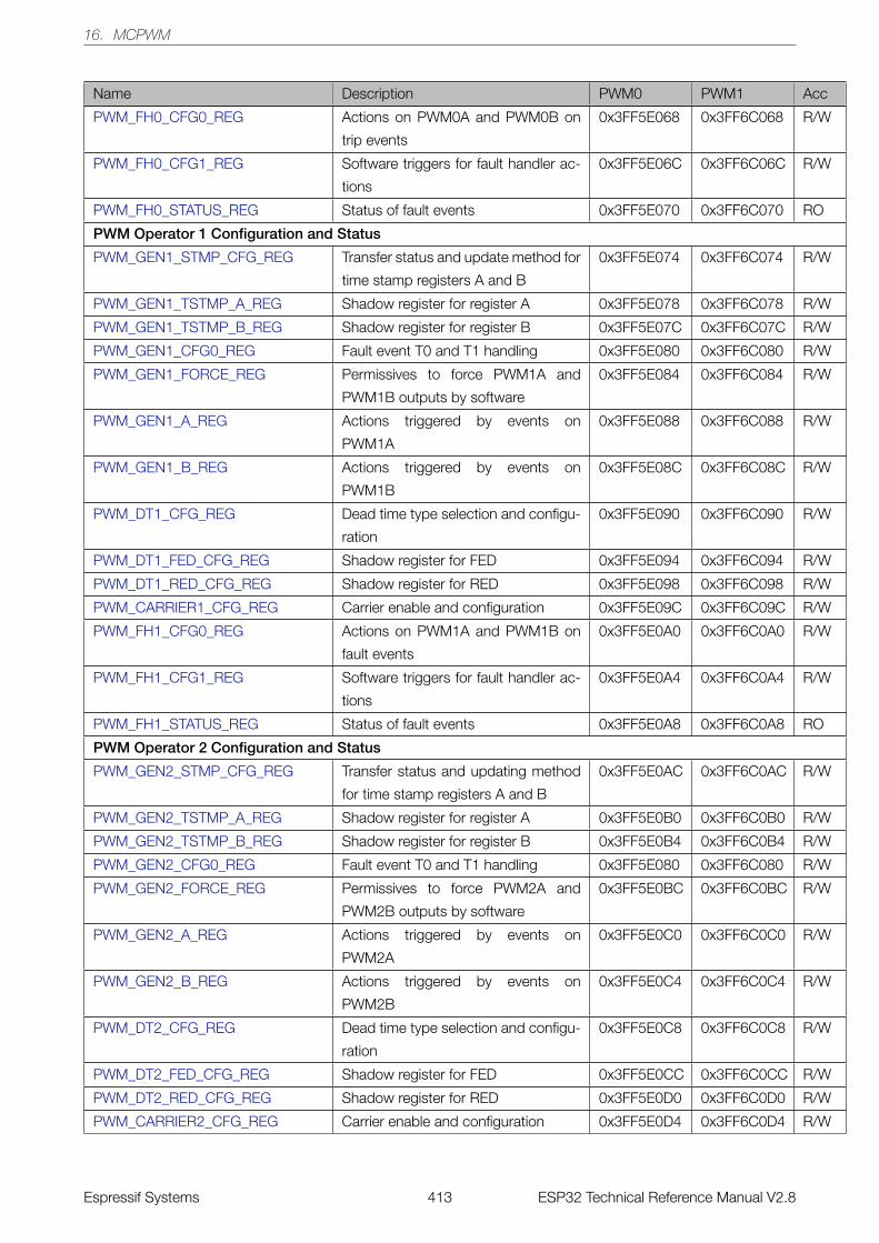
16. MCPWM
Name Description PWM0 PWM1 Acc
PWM_FH0_CFG0_REG Actions on PWM0A and PWM0B on
trip events
0x3FF5E068 0x3FF6C068 R/W
PWM_FH0_CFG1_REG Software triggers for fault handler ac-
tions
0x3FF5E06C 0x3FF6C06C R/W
PWM_FH0_STATUS_REG Status of fault events 0x3FF5E070 0x3FF6C070 RO
PWM Operator 1 Configuration and Status
PWM_GEN1_STMP_CFG_REG Transfer status and update method for
time stamp registers A and B
0x3FF5E074 0x3FF6C074 R/W
PWM_GEN1_TSTMP_A_REG Shadow register for register A 0x3FF5E078 0x3FF6C078 R/W
PWM_GEN1_TSTMP_B_REG Shadow register for register B 0x3FF5E07C 0x3FF6C07C R/W
PWM_GEN1_CFG0_REG Fault event T0 and T1 handling 0x3FF5E080 0x3FF6C080 R/W
PWM_GEN1_FORCE_REG Permissives to force PWM1A and
PWM1B outputs by software
0x3FF5E084 0x3FF6C084 R/W
PWM_GEN1_A_REG Actions triggered by events on
PWM1A
0x3FF5E088 0x3FF6C088 R/W
PWM_GEN1_B_REG Actions triggered by events on
PWM1B
0x3FF5E08C 0x3FF6C08C R/W
PWM_DT1_CFG_REG Dead time type selection and configu-
ration
0x3FF5E090 0x3FF6C090 R/W
PWM_DT1_FED_CFG_REG Shadow register for FED 0x3FF5E094 0x3FF6C094 R/W
PWM_DT1_RED_CFG_REG Shadow register for RED 0x3FF5E098 0x3FF6C098 R/W
PWM_CARRIER1_CFG_REG Carrier enable and configuration 0x3FF5E09C 0x3FF6C09C R/W
PWM_FH1_CFG0_REG Actions on PWM1A and PWM1B on
fault events
0x3FF5E0A0 0x3FF6C0A0 R/W
PWM_FH1_CFG1_REG Software triggers for fault handler ac-
tions
0x3FF5E0A4 0x3FF6C0A4 R/W
PWM_FH1_STATUS_REG Status of fault events 0x3FF5E0A8 0x3FF6C0A8 RO
PWM Operator 2 Configuration and Status
PWM_GEN2_STMP_CFG_REG Transfer status and updating method
for time stamp registers A and B
0x3FF5E0AC 0x3FF6C0AC R/W
PWM_GEN2_TSTMP_A_REG Shadow register for register A 0x3FF5E0B0 0x3FF6C0B0 R/W
PWM_GEN2_TSTMP_B_REG Shadow register for register B 0x3FF5E0B4 0x3FF6C0B4 R/W
PWM_GEN2_CFG0_REG Fault event T0 and T1 handling 0x3FF5E080 0x3FF6C080 R/W
PWM_GEN2_FORCE_REG Permissives to force PWM2A and
PWM2B outputs by software
0x3FF5E0BC 0x3FF6C0BC R/W
PWM_GEN2_A_REG Actions triggered by events on
PWM2A
0x3FF5E0C0 0x3FF6C0C0 R/W
PWM_GEN2_B_REG Actions triggered by events on
PWM2B
0x3FF5E0C4 0x3FF6C0C4 R/W
PWM_DT2_CFG_REG Dead time type selection and configu-
ration
0x3FF5E0C8 0x3FF6C0C8 R/W
PWM_DT2_FED_CFG_REG Shadow register for FED 0x3FF5E0CC 0x3FF6C0CC R/W
PWM_DT2_RED_CFG_REG Shadow register for RED 0x3FF5E0D0 0x3FF6C0D0 R/W
PWM_CARRIER2_CFG_REG Carrier enable and configuration 0x3FF5E0D4 0x3FF6C0D4 R/W
Espressif Systems 413 ESP32 Technical Reference Manual V2.8
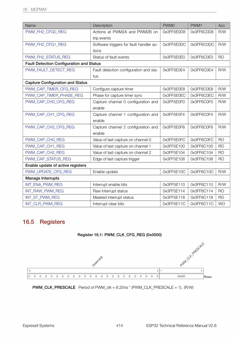
16. MCPWM
Name Description PWM0 PWM1 Acc
PWM_FH2_CFG0_REG Actions at PWM2A and PWM2B on
trip events
0x3FF5E0D8 0x3FF6C0D8 R/W
PWM_FH2_CFG1_REG Software triggers for fault handler ac-
tions
0x3FF5E0DC 0x3FF6C0DC R/W
PWM_FH2_STATUS_REG Status of fault events 0x3FF5E0E0 0x3FF6C0E0 RO
Fault Detection Configuration and Status
PWM_FAULT_DETECT_REG Fault detection configuration and sta-
tus
0x3FF5E0E4 0x3FF6C0E4 R/W
Capture Configuration and Status
PWM_CAP_TIMER_CFG_REG Configure capture timer 0x3FF5E0E8 0x3FF6C0E8 R/W
PWM_CAP_TIMER_PHASE_REG Phase for capture timer sync 0x3FF5E0EC 0x3FF6C0EC R/W
PWM_CAP_CH0_CFG_REG Capture channel 0 configuration and
enable
0x3FF5E0F0 0x3FF6C0F0 R/W
PWM_CAP_CH1_CFG_REG Capture channel 1 configuration and
enable
0x3FF5E0F4 0x3FF6C0F4 R/W
PWM_CAP_CH2_CFG_REG Capture channel 2 configuration and
enable
0x3FF5E0F8 0x3FF6C0F8 R/W
PWM_CAP_CH0_REG Value of last capture on channel 0 0x3FF5E0FC 0x3FF6C0FC RO
PWM_CAP_CH1_REG Value of last capture on channel 1 0x3FF5E100 0x3FF6C100 RO
PWM_CAP_CH2_REG Value of last capture on channel 2 0x3FF5E104 0x3FF6C104 RO
PWM_CAP_STATUS_REG Edge of last capture trigger 0x3FF5E108 0x3FF6C108 RO
Enable update of active registers
PWM_UPDATE_CFG_REG Enable update 0x3FF5E10C 0x3FF6C10C R/W
Manage Interrupts
INT_ENA_PWM_REG Interrupt enable bits 0x3FF5E110 0x3FF6C110 R/W
INT_RAW_PWM_REG Raw interrupt status 0x3FF5E114 0x3FF6C114 RO
INT_ST_PWM_REG Masked interrupt status 0x3FF5E118 0x3FF6C118 RO
INT_CLR_PWM_REG Interrupt clear bits 0x3FF5E11C 0x3FF6C11C WO
16.5 Registers
Register 16.1: PWM_CLK_CFG_REG (0x0000)
(rese
rved)
0 0 0 0 0 0 0 0 0 0 0 0 0 0 0 0 0 0 0 0 0 0 0 0
31 8
PWM
_CLK
_PRESCALE
0x000
7 0
Reset
PWM_CLK_PRESCALE Period of PWM_clk = 6.25ns * (PWM_CLK_PRESCALE + 1). (R/W)
Espressif Systems 414 ESP32 Technical Reference Manual V2.8
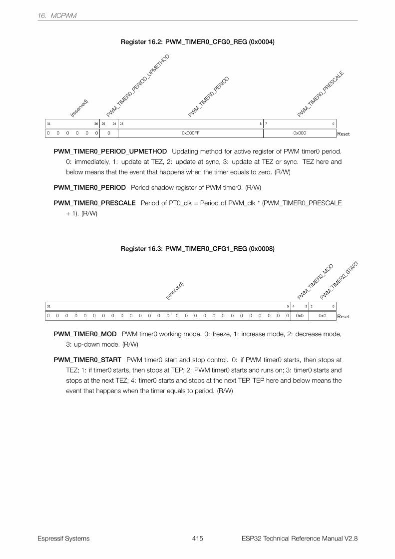
16. MCPWM
Register 16.2: PWM_TIMER0_CFG0_REG (0x0004)
(rese
rved)
0 0 0 0 0 0
31 26
PWM
_TIM
ER0_PERIO
D_UPM
ETHOD
0
25 24
PWM
_TIM
ER0_PERIO
D
0x000FF
23 8
PWM
_TIM
ER0_PRESCALE
0x000
7 0
Reset
PWM_TIMER0_PERIOD_UPMETHOD Updating method for active register of PWM timer0 period.
0: immediately, 1: update at TEZ, 2: update at sync, 3: update at TEZ or sync. TEZ here and
below means that the event that happens when the timer equals to zero. (R/W)
PWM_TIMER0_PERIOD Period shadow register of PWM timer0. (R/W)
PWM_TIMER0_PRESCALE Period of PT0_clk = Period of PWM_clk * (PWM_TIMER0_PRESCALE
+ 1). (R/W)
Register 16.3: PWM_TIMER0_CFG1_REG (0x0008)
(rese
rved)
0 0 0 0 0 0 0 0 0 0 0 0 0 0 0 0 0 0 0 0 0 0 0 0 0 0 0
31 5
PWM
_TIM
ER0_M
OD
0x0
4 3
PWM
_TIM
ER0_STA
RT
0x0
2 0
Reset
PWM_TIMER0_MOD PWM timer0 working mode. 0: freeze, 1: increase mode, 2: decrease mode,
3: up-down mode. (R/W)
PWM_TIMER0_START PWM timer0 start and stop control. 0: if PWM timer0 starts, then stops at
TEZ; 1: if timer0 starts, then stops at TEP; 2: PWM timer0 starts and runs on; 3: timer0 starts and
stops at the next TEZ; 4: timer0 starts and stops at the next TEP. TEP here and below means the
event that happens when the timer equals to period. (R/W)
Espressif Systems 415 ESP32 Technical Reference Manual V2.8

16. MCPWM
Register 16.4: PWM_TIMER0_SYNC_REG (0x000c)
(rese
rved)
0 0 0 0 0 0 0 0 0 0 0
31 21
PWM
_TIM
ER0_PHASE
0
20 4
PWM
_TIM
ER0_SYNCO_S
EL
0
3 2
PWM
_TIM
ER0_SYNC_S
W
0
1
PWM
_TIM
ER0_SYNCI_E
N
0
0
Reset
PWM_TIMER0_PHASE Phase for timer reload at sync event. (R/W)
PWM_TIMER1_SYNCO_SEL PWM timer0 sync_out selection. 0: sync_in; 1: TEZ; 2: TEP; other-
wise: sync_out is always 0. (R/W)
PWM_TIMER1_SYNC_SW Toggling this bit will trigger a software sync. (R/W)
PWM_TIMER1_SYNCI_EN When set, timer reloading with phase on sync input event is enabled.
(R/W)
Register 16.5: PWM_TIMER0_STATUS_REG (0x0010)
(rese
rved)
0 0 0 0 0 0 0 0 0 0 0 0 0 0 0
31 17
PWM
_TIM
ER0_DIR
ECTION
0
16
PWM
_TIM
ER0_VA
LUE
0
15 0
Reset
PWM_TIMER0_DIRECTION Current direction of the PWM timer0 counter. 0: increment, 1: decre-
ment. (RO)
PWM_TIMER0_VALUE Current value of the PWM timer0 counter. (RO)
Espressif Systems 416 ESP32 Technical Reference Manual V2.8
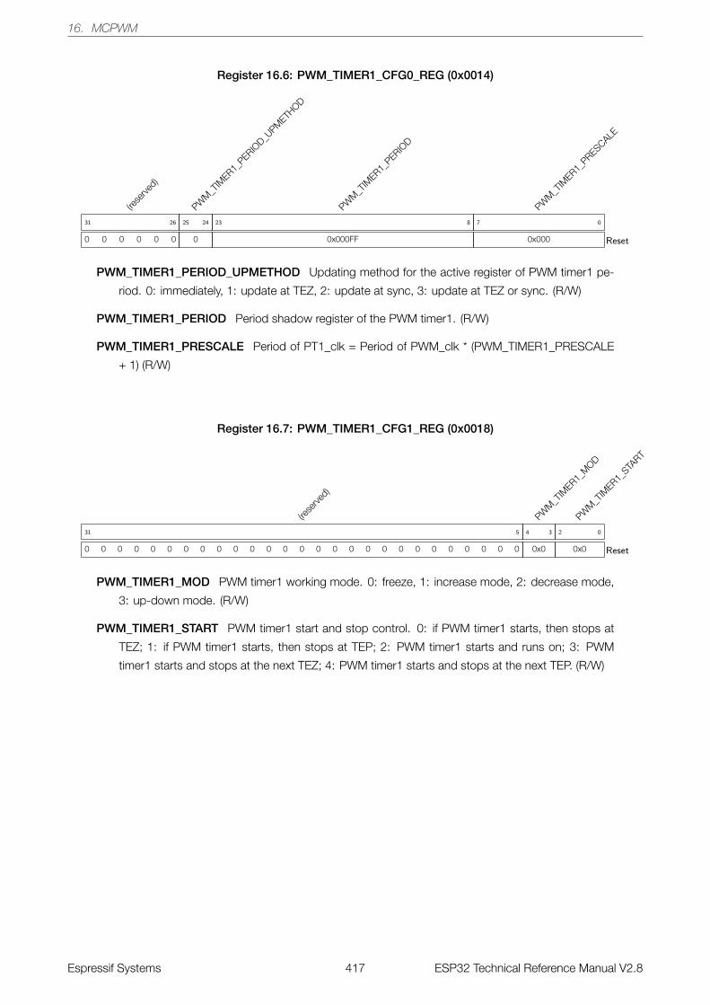
16. MCPWM
Register 16.6: PWM_TIMER1_CFG0_REG (0x0014)
(rese
rved)
0 0 0 0 0 0
31 26
PWM
_TIM
ER1_PERIO
D_UPM
ETHOD
0
25 24
PWM
_TIM
ER1_PERIO
D
0x000FF
23 8
PWM
_TIM
ER1_PRESCALE
0x000
7 0
Reset
PWM_TIMER1_PERIOD_UPMETHOD Updating method for the active register of PWM timer1 pe-
riod. 0: immediately, 1: update at TEZ, 2: update at sync, 3: update at TEZ or sync. (R/W)
PWM_TIMER1_PERIOD Period shadow register of the PWM timer1. (R/W)
PWM_TIMER1_PRESCALE Period of PT1_clk = Period of PWM_clk * (PWM_TIMER1_PRESCALE
+ 1) (R/W)
Register 16.7: PWM_TIMER1_CFG1_REG (0x0018)
(rese
rved)
0 0 0 0 0 0 0 0 0 0 0 0 0 0 0 0 0 0 0 0 0 0 0 0 0 0 0
31 5
PWM
_TIM
ER1_M
OD
0x0
4 3
PWM
_TIM
ER1_STA
RT
0x0
2 0
Reset
PWM_TIMER1_MOD PWM timer1 working mode. 0: freeze, 1: increase mode, 2: decrease mode,
3: up-down mode. (R/W)
PWM_TIMER1_START PWM timer1 start and stop control. 0: if PWM timer1 starts, then stops at
TEZ; 1: if PWM timer1 starts, then stops at TEP; 2: PWM timer1 starts and runs on; 3: PWM
timer1 starts and stops at the next TEZ; 4: PWM timer1 starts and stops at the next TEP. (R/W)
Espressif Systems 417 ESP32 Technical Reference Manual V2.8
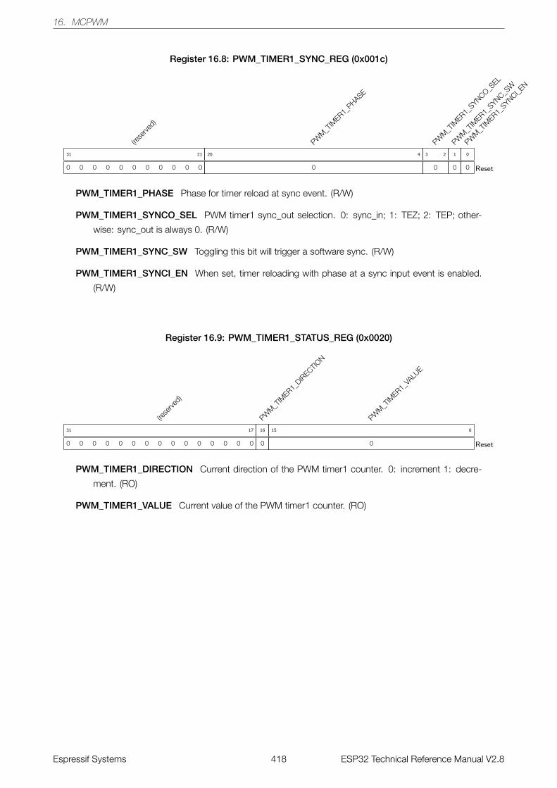
16. MCPWM
Register 16.8: PWM_TIMER1_SYNC_REG (0x001c)
(rese
rved)
0 0 0 0 0 0 0 0 0 0 0
31 21
PWM
_TIM
ER1_PHASE
0
20 4
PWM
_TIM
ER1_SYNCO_S
EL
0
3 2
PWM
_TIM
ER1_SYNC_S
W
0
1
PWM
_TIM
ER1_SYNCI_E
N
0
0
Reset
PWM_TIMER1_PHASE Phase for timer reload at sync event. (R/W)
PWM_TIMER1_SYNCO_SEL PWM timer1 sync_out selection. 0: sync_in; 1: TEZ; 2: TEP; other-
wise: sync_out is always 0. (R/W)
PWM_TIMER1_SYNC_SW Toggling this bit will trigger a software sync. (R/W)
PWM_TIMER1_SYNCI_EN When set, timer reloading with phase at a sync input event is enabled.
(R/W)
Register 16.9: PWM_TIMER1_STATUS_REG (0x0020)
(rese
rved)
0 0 0 0 0 0 0 0 0 0 0 0 0 0 0
31 17
PWM
_TIM
ER1_DIR
ECTION
0
16
PWM
_TIM
ER1_VA
LUE
0
15 0
Reset
PWM_TIMER1_DIRECTION Current direction of the PWM timer1 counter. 0: increment 1: decre-
ment. (RO)
PWM_TIMER1_VALUE Current value of the PWM timer1 counter. (RO)
Espressif Systems 418 ESP32 Technical Reference Manual V2.8

16. MCPWM
Register 16.10: PWM_TIMER2_CFG0_REG (0x0024)
(rese
rved)
0 0 0 0 0 0
31 26
PWM
_TIM
ER2_PERIO
D_UPM
ETHOD
0
25 24
PWM
_TIM
ER2_PERIO
D
0x000FF
23 8
PWM
_TIM
ER2_PRESCALE
0x000
7 0
Reset
PWM_TIMER2_PERIOD_UPMETHOD Updating method for active register of PWM timer2 period.
0: immediately, 1: update at TEZ, 2: update at sync, 3: update at TEZ or sync. (R/W)
PWM_TIMER2_PERIOD Period shadow register of PWM timer2. (R/W)
PWM_TIMER2_PRESCALE Period of PT2_clk = Period of PWM_clk * (PWM_TIMER2_PRESCALE
+ 1). (R/W)
Register 16.11: PWM_TIMER2_CFG1_REG (0x0028)
(rese
rved)
0 0 0 0 0 0 0 0 0 0 0 0 0 0 0 0 0 0 0 0 0 0 0 0 0 0 0
31 5
PWM
_TIM
ER2_M
OD
0x0
4 3
PWM
_TIM
ER2_STA
RT
0x0
2 0
Reset
PWM_TIMER2_MOD PWM timer2 working mode. 0: freeze, 1: increase mode, 2: decrease mode,
3: up-down mode. (R/W)
PWM_TIMER2_START PWM timer2 start and stop control. 0: if PWM timer2 starts, then stops at
TEZ; 1: if PWM timer2 starts, then stops at TEP; 2: PWM timer2 starts and runs on; 3: PWM
timer2 starts and stops at the next TEZ; 4: PWM timer2 starts and stops at the next TEP. (R/W)
Espressif Systems 419 ESP32 Technical Reference Manual V2.8
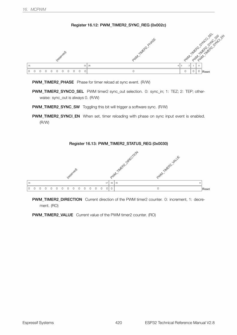
16. MCPWM
Register 16.12: PWM_TIMER2_SYNC_REG (0x002c)
(rese
rved)
0 0 0 0 0 0 0 0 0 0 0
31 21
PWM
_TIM
ER2_PHASE
0
20 4
PWM
_TIM
ER2_SYNCO_S
EL
0
3 2
PWM
_TIM
ER2_SYNC_S
W
0
1
PWM
_TIM
ER2_SYNCI_E
N
0
0
Reset
PWM_TIMER2_PHASE Phase for timer reload at sync event. (R/W)
PWM_TIMER2_SYNCO_SEL PWM timer2 sync_out selection. 0: sync_in; 1: TEZ; 2: TEP; other-
waise: sync_out is always 0. (R/W)
PWM_TIMER2_SYNC_SW Toggling this bit will trigger a software sync. (R/W)
PWM_TIMER2_SYNCI_EN When set, timer reloading with phase on sync input event is enabled.
(R/W)
Register 16.13: PWM_TIMER2_STATUS_REG (0x0030)
(rese
rved)
0 0 0 0 0 0 0 0 0 0 0 0 0 0 0
31 17
PWM
_TIM
ER2_DIR
ECTION
0
16
PWM
_TIM
ER2_VA
LUE
0
15 0
Reset
PWM_TIMER2_DIRECTION Current direction of the PWM timer2 counter. 0: increment, 1: decre-
ment. (RO)
PWM_TIMER2_VALUE Current value of the PWM timer2 counter. (RO)
Espressif Systems 420 ESP32 Technical Reference Manual V2.8
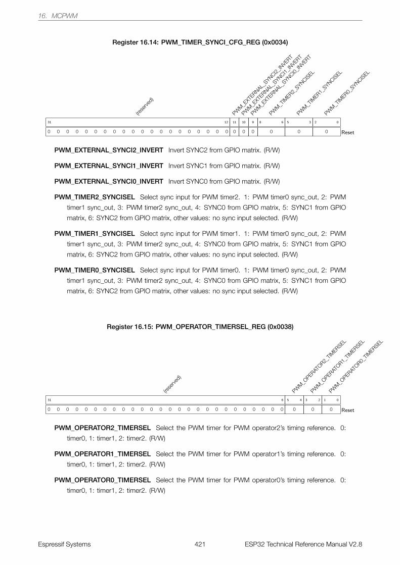
16. MCPWM
Register 16.14: PWM_TIMER_SYNCI_CFG_REG (0x0034)
(rese
rved)
0 0 0 0 0 0 0 0 0 0 0 0 0 0 0 0 0 0 0 0
31 12
PWM
_EXT
ERNAL_SYNCI2_
INVERT
0
11
PWM
_EXT
ERNAL_SYNCI1_
INVERT
0
10
PWM
_EXT
ERNAL_SYNCI0_
INVERT
0
9
PWM
_TIM
ER2_SYNCIS
EL
0
8 6
PWM
_TIM
ER1_SYNCIS
EL
0
5 3
PWM
_TIM
ER0_SYNCIS
EL
0
2 0
Reset
PWM_EXTERNAL_SYNCI2_INVERT Invert SYNC2 from GPIO matrix. (R/W)
PWM_EXTERNAL_SYNCI1_INVERT Invert SYNC1 from GPIO matrix. (R/W)
PWM_EXTERNAL_SYNCI0_INVERT Invert SYNC0 from GPIO matrix. (R/W)
PWM_TIMER2_SYNCISEL Select sync input for PWM timer2. 1: PWM timer0 sync_out, 2: PWM
timer1 sync_out, 3: PWM timer2 sync_out, 4: SYNC0 from GPIO matrix, 5: SYNC1 from GPIO
matrix, 6: SYNC2 from GPIO matrix, other values: no sync input selected. (R/W)
PWM_TIMER1_SYNCISEL Select sync input for PWM timer1. 1: PWM timer0 sync_out, 2: PWM
timer1 sync_out, 3: PWM timer2 sync_out, 4: SYNC0 from GPIO matrix, 5: SYNC1 from GPIO
matrix, 6: SYNC2 from GPIO matrix, other values: no sync input selected. (R/W)
PWM_TIMER0_SYNCISEL Select sync input for PWM timer0. 1: PWM timer0 sync_out, 2: PWM
timer1 sync_out, 3: PWM timer2 sync_out, 4: SYNC0 from GPIO matrix, 5: SYNC1 from GPIO
matrix, 6: SYNC2 from GPIO matrix, other values: no sync input selected. (R/W)
Register 16.15: PWM_OPERATOR_TIMERSEL_REG (0x0038)
(rese
rved)
0 0 0 0 0 0 0 0 0 0 0 0 0 0 0 0 0 0 0 0 0 0 0 0 0 0
31 6
PWM
_OPERAT
OR2_TIM
ERSEL
0
5 4
PWM
_OPERAT
OR1_TIM
ERSEL
0
3 2
PWM
_OPERAT
OR0_TIM
ERSEL
0
1 0
Reset
PWM_OPERATOR2_TIMERSEL Select the PWM timer for PWM operator2’s timing reference. 0:
timer0, 1: timer1, 2: timer2. (R/W)
PWM_OPERATOR1_TIMERSEL Select the PWM timer for PWM operator1’s timing reference. 0:
timer0, 1: timer1, 2: timer2. (R/W)
PWM_OPERATOR0_TIMERSEL Select the PWM timer for PWM operator0’s timing reference. 0:
timer0, 1: timer1, 2: timer2. (R/W)
Espressif Systems 421 ESP32 Technical Reference Manual V2.8
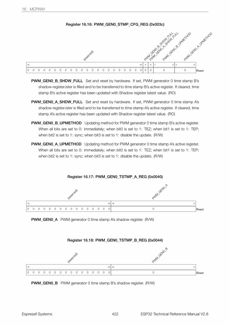
16. MCPWM
Register 16.16: PWM_GEN0_STMP_CFG_REG (0x003c)
(rese
rved)
0 0 0 0 0 0 0 0 0 0 0 0 0 0 0 0 0 0 0 0 0 0
31 10
PWM
_GEN0_
B_SHDW
_FULL
0
9
PWM
_GEN0_
A_SHDW
_FULL
0
8
PWM
_GEN0_
B_UPM
ETHOD
0
7 4
PWM
_GEN0_
A_UPM
ETHOD
0
3 0
Reset
PWM_GEN0_B_SHDW_FULL Set and reset by hardware. If set, PWM generator 0 time stamp B’s
shadow register.ister is filled and to be transferred to time stamp B’s active register. If cleared, time
stamp B’s active register has been updated with Shadow register latest value. (RO)
PWM_GEN0_A_SHDW_FULL Set and reset by hardware. If set, PWM generator 0 time stamp A’s
shadow register.ister is filled and to be transferred to time stamp A’s active register. If cleared, time
stamp A’s active register has been updated with Shadow register latest value. (RO)
PWM_GEN0_B_UPMETHOD Updating method for PWM generator 0 time stamp B’s active register.
When all bits are set to 0: immediately; when bit0 is set to 1: TEZ; when bit1 is set to 1: TEP;
when bit2 is set to 1: sync; when bit3 is set to 1: disable the update. (R/W)
PWM_GEN0_A_UPMETHOD Updating method for PWM generator 0 time stamp A’s active register.
When all bits are set to 0: immediately; when bit0 is set to 1: TEZ; when bit1 is set to 1: TEP;
when bit2 is set to 1: sync; when bit3 is set to 1: disable the update. (R/W)
Register 16.17: PWM_GEN0_TSTMP_A_REG (0x0040)
(rese
rved)
0 0 0 0 0 0 0 0 0 0 0 0 0 0 0 0
31 16
PWM
_GEN0_
A
0
15 0
Reset
PWM_GEN0_A PWM generator 0 time stamp A’s shadow register. (R/W)
Register 16.18: PWM_GEN0_TSTMP_B_REG (0x0044)
(rese
rved)
0 0 0 0 0 0 0 0 0 0 0 0 0 0 0 0
31 16
PWM
_GEN0_
B
0
15 0
Reset
PWM_GEN0_B PWM generator 0 time stamp B’s shadow register. (R/W)
Espressif Systems 422 ESP32 Technical Reference Manual V2.8
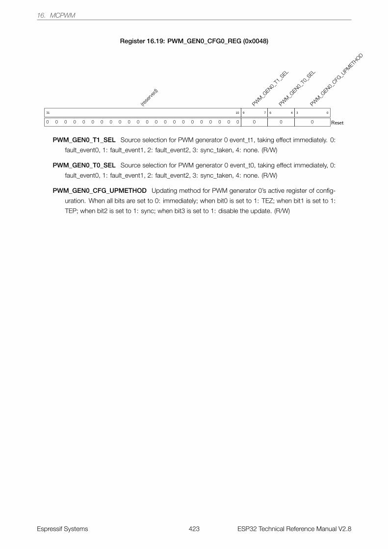
16. MCPWM
Register 16.19: PWM_GEN0_CFG0_REG (0x0048)
(rese
rved)
0 0 0 0 0 0 0 0 0 0 0 0 0 0 0 0 0 0 0 0 0 0
31 10
PWM
_GEN0_
T1_S
EL
0
9 7
PWM
_GEN0_
T0_S
EL
0
6 4
PWM
_GEN0_
CFG_U
PMETH
OD
0
3 0
Reset
PWM_GEN0_T1_SEL Source selection for PWM generator 0 event_t1, taking effect immediately. 0:
fault_event0, 1: fault_event1, 2: fault_event2, 3: sync_taken, 4: none. (R/W)
PWM_GEN0_T0_SEL Source selection for PWM generator 0 event_t0, taking effect immediately, 0:
fault_event0, 1: fault_event1, 2: fault_event2, 3: sync_taken, 4: none. (R/W)
PWM_GEN0_CFG_UPMETHOD Updating method for PWM generator 0’s active register of config-
uration. When all bits are set to 0: immediately; when bit0 is set to 1: TEZ; when bit1 is set to 1:
TEP; when bit2 is set to 1: sync; when bit3 is set to 1: disable the update. (R/W)
Espressif Systems 423 ESP32 Technical Reference Manual V2.8
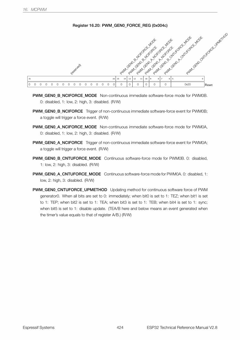
16. MCPWM
Register 16.20: PWM_GEN0_FORCE_REG (0x004c)
(rese
rved)
0 0 0 0 0 0 0 0 0 0 0 0 0 0 0 0
31 16
PWM
_GEN0_
B_NCIFO
RCE_MODE
0
15 14
PWM
_GEN0_
B_NCIFO
RCE
0
13
PWM
_GEN0_
A_NCIFO
RCE_MODE
0
12 11
PWM
_GEN0_
A_NCIFO
RCE
0
10
PWM
_GEN0_
B_CNTU
FORCE_M
ODE
0
9 8
PWM
_GEN0_
A_CNTU
FORCE_M
ODE
0
7 6
PWM
_GEN0_
CNTUFO
RCE_UPM
ETHOD
0x20
5 0
Reset
PWM_GEN0_B_NCIFORCE_MODE Non-continuous immediate software-force mode for PWM0B.
0: disabled, 1: low, 2: high, 3: disabled. (R/W)
PWM_GEN0_B_NCIFORCE Trigger of non-continuous immediate software-force event for PWM0B;
a toggle will trigger a force event. (R/W)
PWM_GEN0_A_NCIFORCE_MODE Non-continuous immediate software-force mode for PWM0A,
0: disabled, 1: low, 2: high, 3: disabled. (R/W)
PWM_GEN0_A_NCIFORCE Trigger of non-continuous immediate software-force event for PWM0A;
a toggle will trigger a force event. (R/W)
PWM_GEN0_B_CNTUFORCE_MODE Continuous software-force mode for PWM0B. 0: disabled,
1: low, 2: high, 3: disabled. (R/W)
PWM_GEN0_A_CNTUFORCE_MODE Continuous software-force mode for PWM0A. 0: disabled, 1:
low, 2: high, 3: disabled. (R/W)
PWM_GEN0_CNTUFORCE_UPMETHOD Updating method for continuous software force of PWM
generator0. When all bits are set to 0: immediately; when bit0 is set to 1: TEZ; when bit1 is set
to 1: TEP; when bit2 is set to 1: TEA; when bit3 is set to 1: TEB; when bit4 is set to 1: sync;
when bit5 is set to 1: disable update. (TEA/B here and below means an event generated when
the timer’s value equals to that of register A/B.) (R/W)
Espressif Systems 424 ESP32 Technical Reference Manual V2.8

16. MCPWM
Register 16.21: PWM_GEN0_A_REG (0x0050)
(rese
rved)
0 0 0 0 0 0 0 0
31 24
PWM
_GEN0_
A_DT1
0
23 22
PWM
_GEN0_
A_DT0
0
21 20
PWM
_GEN0_
A_DTE
B
0
19 18
PWM
_GEN0_
A_DTE
A
0
17 16
PWM
_GEN0_
A_DTE
P
0
15 14
PWM
_GEN0_
A_DTE
Z
0
13 12
PWM
_GEN0_
A_UT1
0
11 10
PWM
_GEN0_
A_UT0
0
9 8
PWM
_GEN0_
A_UTE
B
0
7 6
PWM
_GEN0_
A_UTE
A
0
5 4
PWM
_GEN0_
A_UTE
P
0
3 2
PWM
_GEN0_
A_UTE
Z
0
1 0
Reset
PWM_GEN0_A_DT1 Action on PWM0A triggered by event_t1 when the timer decreases. 0: no
change, 1: low, 2: high, 3: toggle. (R/W)
PWM_GEN0_A_DT0 Action on PWM0A triggered by event_t0 when the timer decreases. (R/W)
PWM_GEN0_A_DTEB Action on PWM0A triggered by event TEB when the timer decreases. (R/W)
PWM_GEN0_A_DTEA Action on PWM0A triggered by event TEA when the timer decreases. (R/W)
PWM_GEN0_A_DTEP Action on PWM0A triggered by event TEP when the timer decreases. (R/W)
PWM_GEN0_A_DTEZ Action on PWM0A triggered by event TEZ when the timer decreases. (R/W)
PWM_GEN0_A_UT1 Action on PWM0A triggered by event_t1 when the timer increases. (R/W)
PWM_GEN0_A_UT0 Action on PWM0A triggered by event_t0 when the timer increases. (R/W)
PWM_GEN0_A_UTEB Action on PWM0A triggered by event TEB when the timer increases. (R/W)
PWM_GEN0_A_UTEA Action on PWM0A triggered by event TEA when the timer increases. (R/W)
PWM_GEN0_A_UTEP Action on PWM0A triggered by event TEP when the timer increases. (R/W)
PWM_GEN0_A_UTEZ Action on PWM0A triggered by event TEZ when the timer increases. (R/W)
Espressif Systems 425 ESP32 Technical Reference Manual V2.8
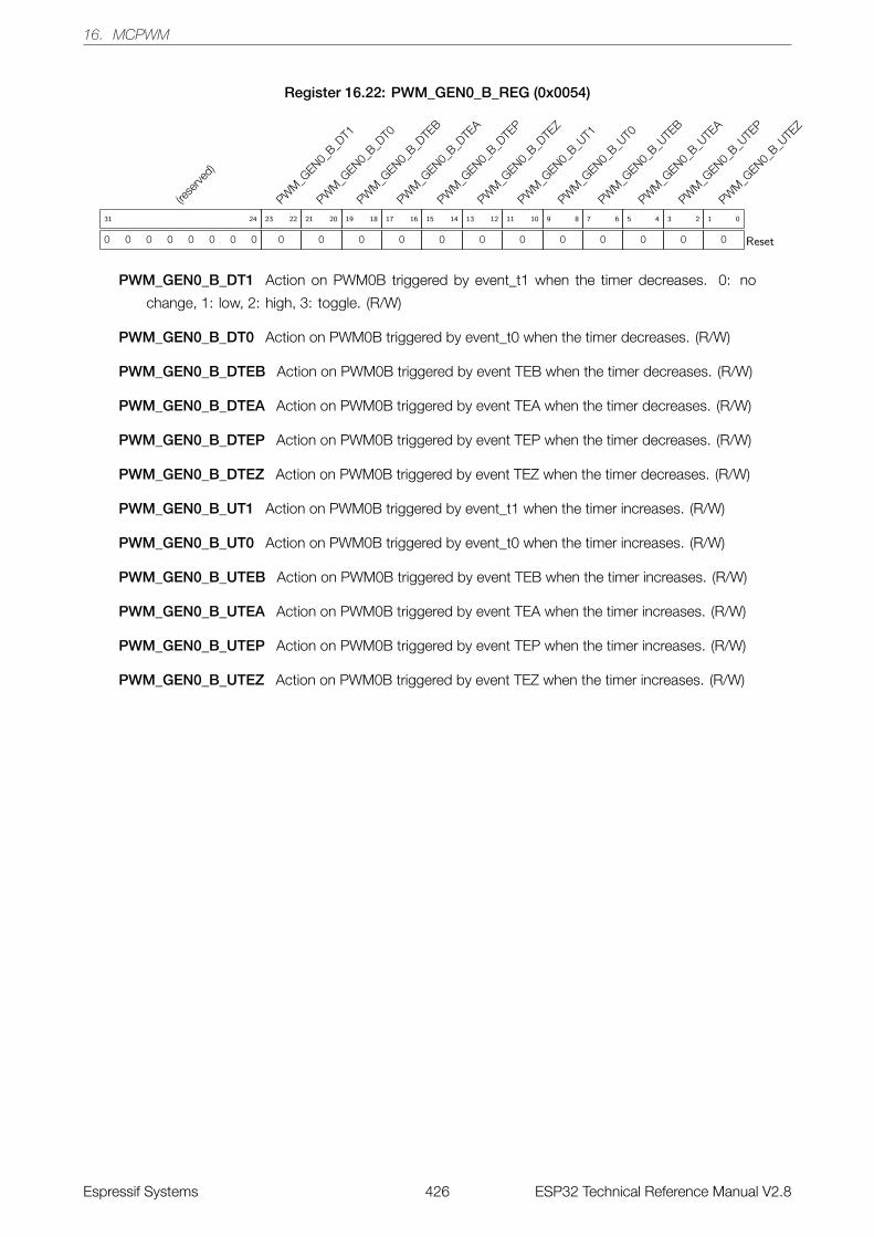
16. MCPWM
Register 16.22: PWM_GEN0_B_REG (0x0054)
(rese
rved)
0 0 0 0 0 0 0 0
31 24
PWM
_GEN0_
B_DT1
0
23 22
PWM
_GEN0_
B_DT0
0
21 20
PWM
_GEN0_
B_DTE
B
0
19 18
PWM
_GEN0_
B_DTE
A
0
17 16
PWM
_GEN0_
B_DTE
P
0
15 14
PWM
_GEN0_
B_DTE
Z
0
13 12
PWM
_GEN0_
B_UT1
0
11 10
PWM
_GEN0_
B_UT0
0
9 8
PWM
_GEN0_
B_UTE
B
0
7 6
PWM
_GEN0_
B_UTE
A
0
5 4
PWM
_GEN0_
B_UTE
P
0
3 2
PWM
_GEN0_
B_UTE
Z
0
1 0
Reset
PWM_GEN0_B_DT1 Action on PWM0B triggered by event_t1 when the timer decreases. 0: no
change, 1: low, 2: high, 3: toggle. (R/W)
PWM_GEN0_B_DT0 Action on PWM0B triggered by event_t0 when the timer decreases. (R/W)
PWM_GEN0_B_DTEB Action on PWM0B triggered by event TEB when the timer decreases. (R/W)
PWM_GEN0_B_DTEA Action on PWM0B triggered by event TEA when the timer decreases. (R/W)
PWM_GEN0_B_DTEP Action on PWM0B triggered by event TEP when the timer decreases. (R/W)
PWM_GEN0_B_DTEZ Action on PWM0B triggered by event TEZ when the timer decreases. (R/W)
PWM_GEN0_B_UT1 Action on PWM0B triggered by event_t1 when the timer increases. (R/W)
PWM_GEN0_B_UT0 Action on PWM0B triggered by event_t0 when the timer increases. (R/W)
PWM_GEN0_B_UTEB Action on PWM0B triggered by event TEB when the timer increases. (R/W)
PWM_GEN0_B_UTEA Action on PWM0B triggered by event TEA when the timer increases. (R/W)
PWM_GEN0_B_UTEP Action on PWM0B triggered by event TEP when the timer increases. (R/W)
PWM_GEN0_B_UTEZ Action on PWM0B triggered by event TEZ when the timer increases. (R/W)
Espressif Systems 426 ESP32 Technical Reference Manual V2.8
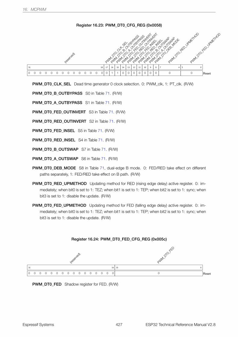
16. MCPWM
Register 16.23: PWM_DT0_CFG_REG (0x0058)
(rese
rved)
0 0 0 0 0 0 0 0 0 0 0 0 0 0
31 18
PWM
_DT0
_CLK
_SEL
0
17
PWM
_DT0
_B_O
UTBYPA
SS
1
16
PWM
_DT0
_A_O
UTBYPA
SS
1
15
PWM
_DT0
_FED_O
UTINVERT
0
14
PWM
_DT0
_RED_O
UTINVERT
0
13
PWM
_DT0
_FED_IN
SEL
0
12
PWM
_DT0
_RED_IN
SEL
0
11
PWM
_DT0
_B_O
UTSW
AP
0
10
PWM
_DT0
_A_O
UTSW
AP
0
9
PWM
_DT0
_DEB_M
ODE
0
8
PWM
_DT0
_RED_U
PMETH
OD
0
7 4
PWM
_DT0
_FED_U
PMETH
OD
0
3 0
Reset
PWM_DT0_CLK_SEL Dead time generator 0 clock selection. 0: PWM_clk, 1: PT_clk. (R/W)
PWM_DT0_B_OUTBYPASS S0 in Table 71. (R/W)
PWM_DT0_A_OUTBYPASS S1 in Table 71. (R/W)
PWM_DT0_FED_OUTINVERT S3 in Table 71. (R/W)
PWM_DT0_RED_OUTINVERT S2 in Table 71. (R/W)
PWM_DT0_FED_INSEL S5 in Table 71. (R/W)
PWM_DT0_RED_INSEL S4 in Table 71. (R/W)
PWM_DT0_B_OUTSWAP S7 in Table 71. (R/W)
PWM_DT0_A_OUTSWAP S6 in Table 71. (R/W)
PWM_DT0_DEB_MODE S8 in Table 71, dual-edge B mode. 0: FED/RED take effect on different
paths separately, 1: FED/RED take effect on B path. (R/W)
PWM_DT0_RED_UPMETHOD Updating method for RED (rising edge delay) active register. 0: im-
mediately; when bit0 is set to 1: TEZ; when bit1 is set to 1: TEP; when bit2 is set to 1: sync; when
bit3 is set to 1: disable the update. (R/W)
PWM_DT0_FED_UPMETHOD Updating method for FED (falling edge delay) active register. 0: im-
mediately; when bit0 is set to 1: TEZ; when bit1 is set to 1: TEP; when bit2 is set to 1: sync; when
bit3 is set to 1: disable the update. (R/W)
Register 16.24: PWM_DT0_FED_CFG_REG (0x005c)
(rese
rved)
0 0 0 0 0 0 0 0 0 0 0 0 0 0 0 0
31 16
PWM
_DT0
_FED
0
15 0
Reset
PWM_DT0_FED Shadow register for FED. (R/W)
Espressif Systems 427 ESP32 Technical Reference Manual V2.8

16. MCPWM
Register 16.25: PWM_DT0_RED_CFG_REG (0x0060)
(rese
rved)
0 0 0 0 0 0 0 0 0 0 0 0 0 0 0 0
31 16
PWM
_DT0
_RED
0
15 0
Reset
PWM_DT0_RED Shadow register for RED. (R/W)
Register 16.26: PWM_CARRIER0_CFG_REG (0x0064)
(rese
rved)
0 0 0 0 0 0 0 0 0 0 0 0 0 0 0 0 0 0
31 14
PWM
_CARRIER0_
IN_IN
VERT
0
13
PWM
_CARRIER0_
OUT_IN
VERT
0
12
PWM
_CARRIER0_
OSHWTH
0
11 8
PWM
_CARRIER0_
DUTY
0
7 5
PWM
_CARRIER0_
PRESCALE
0
4 1
PWM
_CARRIER0_
EN
0
0
Reset
PWM_CARRIER0_IN_INVERT When set, invert the input of PWM0A and PWM0B for this submodule.
(R/W)
PWM_CARRIER0_OUT_INVERT When set, invert the output of PWM0A and PWM0B for this sub-
module. (R/W)
PWM_CARRIER0_OSHWTH Width of the first pulse�in number of periods of the carrier. (R/W)
PWM_CARRIER0_DUTY Carrier duty selection. Duty = PWM_CARRIER0_DUTY/8. (R/W)
PWM_CARRIER0_PRESCALE PWM carrier0 clock (PC_clk) prescale value. Period of PC_clk = pe-
riod of PWM_clk * (PWM_CARRIER0_PRESCALE + 1). (R/W)
PWM_CARRIER0_EN When set, carrier0 function is enabled. When cleared, carrier0 is bypassed.
(R/W)
Espressif Systems 428 ESP32 Technical Reference Manual V2.8

16. MCPWM
Register 16.27: PWM_FH0_CFG0_REG (0x0068)
(rese
rved)
0 0 0 0 0 0 0 0
31 24
PWM
_FH0_
B_OST_
U
0
23 22
PWM
_FH0_
B_OST_
D
0
21 20
PWM
_FH0_
B_CBC_U
0
19 18
PWM
_FH0_
B_CBC_D
0
17 16
PWM
_FH0_
A_OST_
U
0
15 14
PWM
_FH0_
A_OST_
D
0
13 12
PWM
_FH0_
A_CBC_U
0
11 10
PWM
_FH0_
A_CBC_D
0
9 8
PWM
_FH0_
F0_O
ST
0
7
PWM
_FH0_
F1_O
ST
0
6
PWM
_FH0_
F2_O
ST
0
5
PWM
_FH0_
SW_O
ST
0
4
PWM
_FH0_
F0_C
BC
0
3
PWM
_FH0_
F1_C
BC
0
2
PWM
_FH0_
F2_C
BC
0
1
PWM
_FH0_
SW_C
BC
0
0
Reset
PWM_FH0_B_OST_U One-shot mode action on PWM0B when a fault event occurs and the timer is
increasing. 0: do nothing, 1: force low, 2: force high, 3: toggle. (R/W)
PWM_FH0_B_OST_D One-shot mode action on PWM0B when a fault event occurs and the timer is
decreasing. 0: do nothing, 1: force low, 2: force high, 3: toggle. (R/W)
PWM_FH0_B_CBC_U Cycle-by-cycle mode action on PWM0B when a fault event occurs and the
timer is increasing. 0: do nothing, 1: force low, 2: force high, 3: toggle. (R/W)
PWM_FH0_B_CBC_D Cycle-by-cycle mode action on PWM0B when a fault event occurs and the
timer is decreasing. 0: do nothing, 1: force low, 2: force high, 3: toggle. (R/W)
PWM_FH0_A_OST_U One-shot mode action on PWM0A when a fault event occurs and the timer is
increasing. 0: do nothing, 1: force low, 2: force high, 3: toggle. (R/W)
PWM_FH0_A_OST_D One-shot mode action on PWM0A when a fault event occurs and the timer is
decreasing. 0: do nothing, 1: force low, 2: force high, 3: toggle. (R/W)
PWM_FH0_A_CBC_U Cycle-by-cycle mode action on PWM0A when a fault event occurs and the
timer is increasing. 0: do nothing, 1: force low, 2: force high, 3: toggle. (R/W)
PWM_FH0_A_CBC_D Cycle-by-cycle mode action on PWM0A when a fault event occurs and the
timer is decreasing. 0: do nothing, 1: force low, 2: force high, 3: toggle. (R/W)
PWM_FH0_F0_OST event_f0 will trigger one-shot mode action. 0: disable, 1: enable. (R/W)
PWM_FH0_F1_OST event_f1 will trigger one-shot mode action. 0: disable, 1: enable. (R/W)
PWM_FH0_F2_OST event_f2 will trigger one-shot mode action. 0: disable, 1: enable. (R/W)
PWM_FH0_SW_OST Enable register for software-forced one-shot mode action. 0: disable, 1: en-
able. (R/W)
PWM_FH0_F0_CBC event_f0 will trigger cycle-by-cycle mode action. 0: disable, 1: enable. (R/W)
PWM_FH0_F1_CBC event_f1 will trigger cycle-by-cycle mode action. 0: disable, 1: enable. (R/W)
PWM_FH0_F2_CBC event_f2 will trigger cycle-by-cycle mode action. 0: disable, 1: enable. (R/W)
PWM_FH0_SW_CBC Enable register for software-forced cycle-by-cycle mode action. 0: disable, 1:
enable. (R/W)
Espressif Systems 429 ESP32 Technical Reference Manual V2.8
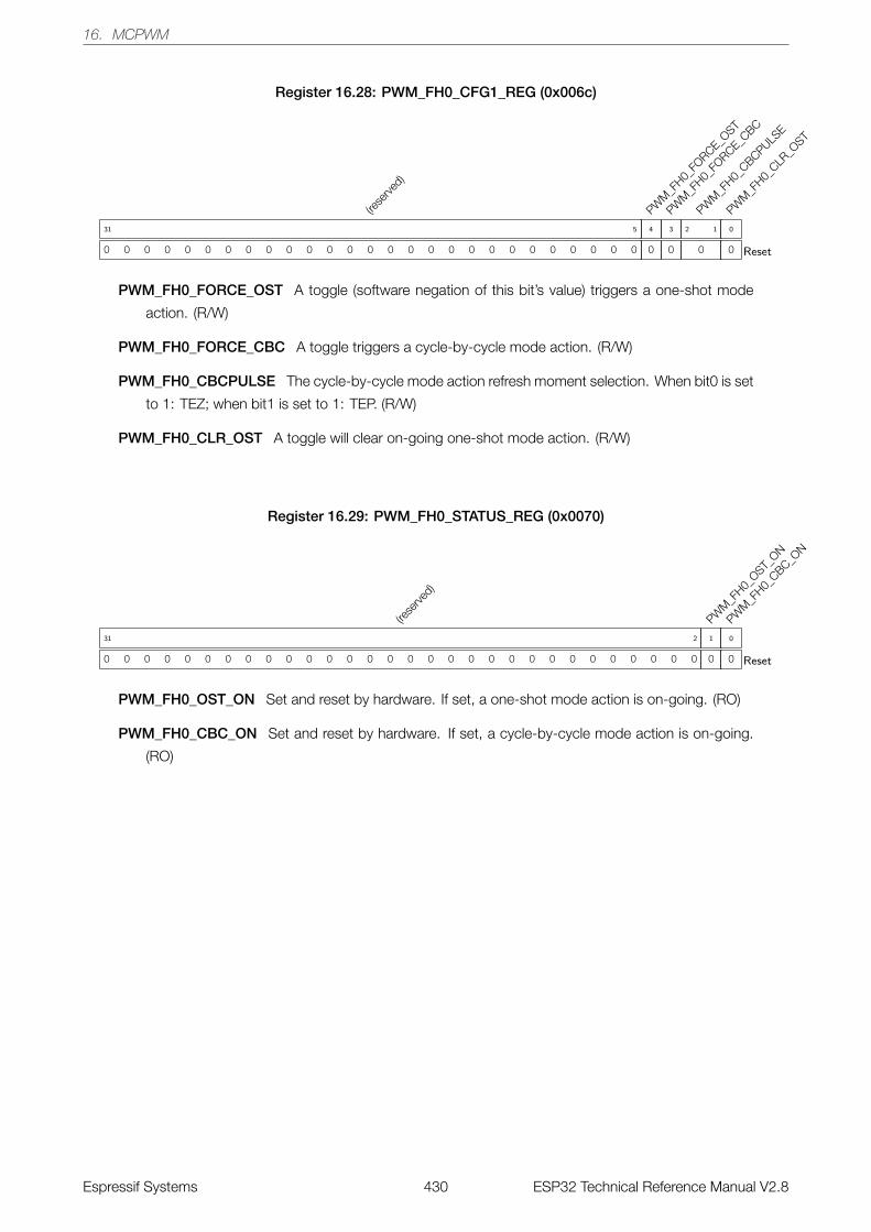
16. MCPWM
Register 16.28: PWM_FH0_CFG1_REG (0x006c)
(rese
rved)
0 0 0 0 0 0 0 0 0 0 0 0 0 0 0 0 0 0 0 0 0 0 0 0 0 0 0
31 5
PWM
_FH0_
FORCE_O
ST
0
4
PWM
_FH0_
FORCE_C
BC
0
3
PWM
_FH0_
CBCPULSE
0
2 1
PWM
_FH0_
CLR_O
ST
0
0
Reset
PWM_FH0_FORCE_OST A toggle (software negation of this bit’s value) triggers a one-shot mode
action. (R/W)
PWM_FH0_FORCE_CBC A toggle triggers a cycle-by-cycle mode action. (R/W)
PWM_FH0_CBCPULSE The cycle-by-cycle mode action refresh moment selection. When bit0 is set
to 1: TEZ; when bit1 is set to 1: TEP. (R/W)
PWM_FH0_CLR_OST A toggle will clear on-going one-shot mode action. (R/W)
Register 16.29: PWM_FH0_STATUS_REG (0x0070)
(rese
rved)
0 0 0 0 0 0 0 0 0 0 0 0 0 0 0 0 0 0 0 0 0 0 0 0 0 0 0 0 0 0
31 2
PWM
_FH0_
OST_ON
0
1
PWM
_FH0_
CBC_ON
0
0
Reset
PWM_FH0_OST_ON Set and reset by hardware. If set, a one-shot mode action is on-going. (RO)
PWM_FH0_CBC_ON Set and reset by hardware. If set, a cycle-by-cycle mode action is on-going.
(RO)
Espressif Systems 430 ESP32 Technical Reference Manual V2.8
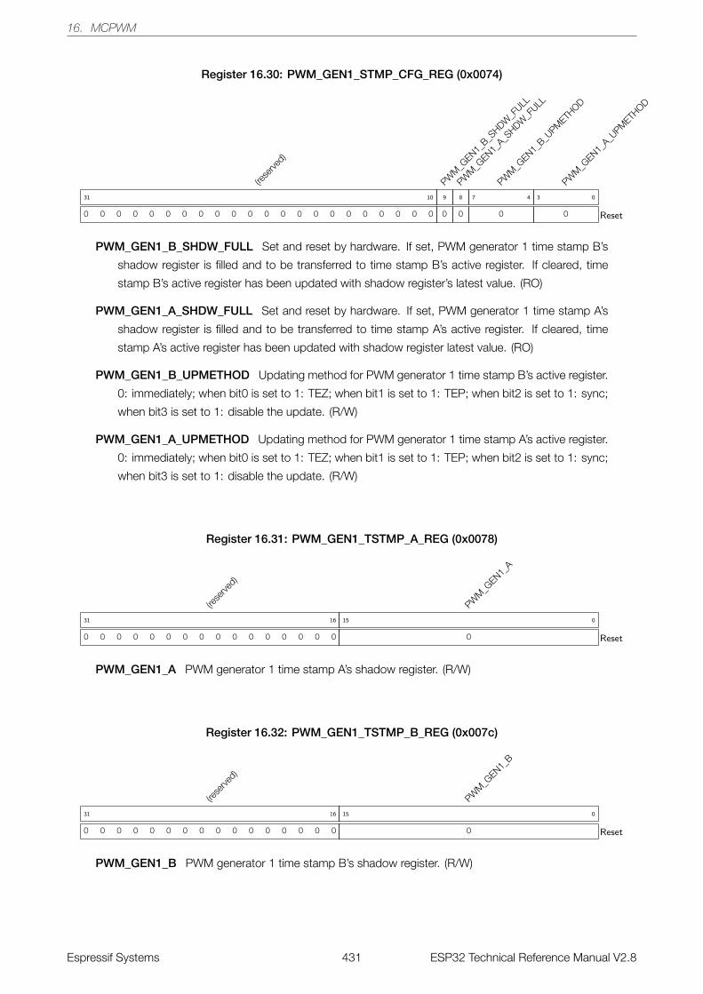
16. MCPWM
Register 16.30: PWM_GEN1_STMP_CFG_REG (0x0074)
(rese
rved)
0 0 0 0 0 0 0 0 0 0 0 0 0 0 0 0 0 0 0 0 0 0
31 10
PWM
_GEN1_
B_SHDW
_FULL
0
9
PWM
_GEN1_
A_SHDW
_FULL
0
8
PWM
_GEN1_
B_UPM
ETHOD
0
7 4
PWM
_GEN1_
A_UPM
ETHOD
0
3 0
Reset
PWM_GEN1_B_SHDW_FULL Set and reset by hardware. If set, PWM generator 1 time stamp B’s
shadow register is filled and to be transferred to time stamp B’s active register. If cleared, time
stamp B’s active register has been updated with shadow register’s latest value. (RO)
PWM_GEN1_A_SHDW_FULL Set and reset by hardware. If set, PWM generator 1 time stamp A’s
shadow register is filled and to be transferred to time stamp A’s active register. If cleared, time
stamp A’s active register has been updated with shadow register latest value. (RO)
PWM_GEN1_B_UPMETHOD Updating method for PWM generator 1 time stamp B’s active register.
0: immediately; when bit0 is set to 1: TEZ; when bit1 is set to 1: TEP; when bit2 is set to 1: sync;
when bit3 is set to 1: disable the update. (R/W)
PWM_GEN1_A_UPMETHOD Updating method for PWM generator 1 time stamp A’s active register.
0: immediately; when bit0 is set to 1: TEZ; when bit1 is set to 1: TEP; when bit2 is set to 1: sync;
when bit3 is set to 1: disable the update. (R/W)
Register 16.31: PWM_GEN1_TSTMP_A_REG (0x0078)
(rese
rved)
0 0 0 0 0 0 0 0 0 0 0 0 0 0 0 0
31 16
PWM
_GEN1_
A
0
15 0
Reset
PWM_GEN1_A PWM generator 1 time stamp A’s shadow register. (R/W)
Register 16.32: PWM_GEN1_TSTMP_B_REG (0x007c)
(rese
rved)
0 0 0 0 0 0 0 0 0 0 0 0 0 0 0 0
31 16
PWM
_GEN1_
B
0
15 0
Reset
PWM_GEN1_B PWM generator 1 time stamp B’s shadow register. (R/W)
Espressif Systems 431 ESP32 Technical Reference Manual V2.8
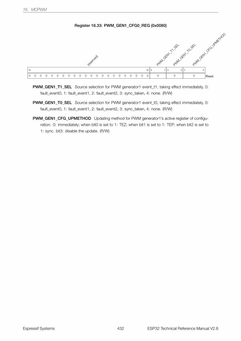
16. MCPWM
Register 16.33: PWM_GEN1_CFG0_REG (0x0080)
(rese
rved)
0 0 0 0 0 0 0 0 0 0 0 0 0 0 0 0 0 0 0 0 0 0
31 10
PWM
_GEN1_
T1_S
EL
0
9 7
PWM
_GEN1_
T0_S
EL
0
6 4
PWM
_GEN1_
CFG_U
PMETH
OD
0
3 0
Reset
PWM_GEN1_T1_SEL Source selection for PWM generator1 event_t1, taking effect immediately, 0:
fault_event0, 1: fault_event1, 2: fault_event2, 3: sync_taken, 4: none. (R/W)
PWM_GEN1_T0_SEL Source selection for PWM generator1 event_t0, taking effect immediately, 0:
fault_event0, 1: fault_event1, 2: fault_event2, 3: sync_taken, 4: none. (R/W)
PWM_GEN1_CFG_UPMETHOD Updating method for PWM generator1’s active register of configu-
ration. 0: immediately; when bit0 is set to 1: TEZ; when bit1 is set to 1: TEP; when bit2 is set to
1: sync. bit3: disable the update. (R/W)
Espressif Systems 432 ESP32 Technical Reference Manual V2.8
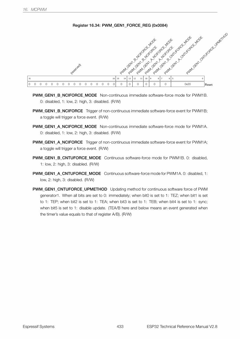
16. MCPWM
Register 16.34: PWM_GEN1_FORCE_REG (0x0084)
(rese
rved)
0 0 0 0 0 0 0 0 0 0 0 0 0 0 0 0
31 16
PWM
_GEN1_
B_NCIFO
RCE_MODE
0
15 14
PWM
_GEN1_
B_NCIFO
RCE
0
13
PWM
_GEN1_
A_NCIFO
RCE_MODE
0
12 11
PWM
_GEN1_
A_NCIFO
RCE
0
10
PWM
_GEN1_
B_CNTU
FORCE_M
ODE
0
9 8
PWM
_GEN1_
A_CNTU
FORCE_M
ODE
0
7 6
PWM
_GEN1_
CNTUFO
RCE_UPM
ETHOD
0x20
5 0
Reset
PWM_GEN1_B_NCIFORCE_MODE Non-continuous immediate software-force mode for PWM1B.
0: disabled, 1: low, 2: high, 3: disabled. (R/W)
PWM_GEN1_B_NCIFORCE Trigger of non-continuous immediate software-force event for PWM1B;
a toggle will trigger a force event. (R/W)
PWM_GEN1_A_NCIFORCE_MODE Non-continuous immediate software-force mode for PWM1A.
0: disabled, 1: low, 2: high, 3: disabled. (R/W)
PWM_GEN1_A_NCIFORCE Trigger of non-continuous immediate software-force event for PWM1A;
a toggle will trigger a force event. (R/W)
PWM_GEN1_B_CNTUFORCE_MODE Continuous software-force mode for PWM1B. 0: disabled,
1: low, 2: high, 3: disabled. (R/W)
PWM_GEN1_A_CNTUFORCE_MODE Continuous software-force mode for PWM1A. 0: disabled, 1:
low, 2: high, 3: disabled. (R/W)
PWM_GEN1_CNTUFORCE_UPMETHOD Updating method for continuous software force of PWM
generator1. When all bits are set to 0: immediately; when bit0 is set to 1: TEZ; when bit1 is set
to 1: TEP; when bit2 is set to 1: TEA; when bit3 is set to 1: TEB; when bit4 is set to 1: sync;
when bit5 is set to 1: disable update. (TEA/B here and below means an event generated when
the timer’s value equals to that of register A/B). (R/W)
Espressif Systems 433 ESP32 Technical Reference Manual V2.8
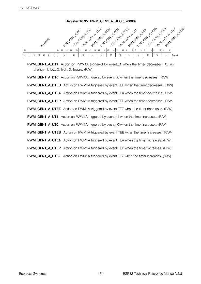
16. MCPWM
Register 16.35: PWM_GEN1_A_REG (0x0088)
(rese
rved)
0 0 0 0 0 0 0 0
31 24
PWM
_GEN1_
A_DT1
0
23 22
PWM
_GEN1_
A_DT0
0
21 20
PWM
_GEN1_
A_DTE
B
0
19 18
PWM
_GEN1_
A_DTE
A
0
17 16
PWM
_GEN1_
A_DTE
P
0
15 14
PWM
_GEN1_
A_DTE
Z
0
13 12
PWM
_GEN1_
A_UT1
0
11 10
PWM
_GEN1_
A_UT0
0
9 8
PWM
_GEN1_
A_UTE
B
0
7 6
PWM
_GEN1_
A_UTE
A
0
5 4
PWM
_GEN1_
A_UTE
P
0
3 2
PWM
_GEN1_
A_UTE
Z
0
1 0
Reset
PWM_GEN1_A_DT1 Action on PWM1A triggered by event_t1 when the timer decreases. 0: no
change, 1: low, 2: high, 3: toggle. (R/W)
PWM_GEN1_A_DT0 Action on PWM1A triggered by event_t0 when the timer decreases. (R/W)
PWM_GEN1_A_DTEB Action on PWM1A triggered by event TEB when the timer decreases. (R/W)
PWM_GEN1_A_DTEA Action on PWM1A triggered by event TEA when the timer decreases. (R/W)
PWM_GEN1_A_DTEP Action on PWM1A triggered by event TEP when the timer decreases. (R/W)
PWM_GEN1_A_DTEZ Action on PWM1A triggered by event TEZ when the timer decreases. (R/W)
PWM_GEN1_A_UT1 Action on PWM1A triggered by event_t1 when the timer increases. (R/W)
PWM_GEN1_A_UT0 Action on PWM1A triggered by event_t0 when the timer increases. (R/W)
PWM_GEN1_A_UTEB Action on PWM1A triggered by event TEB when the timer increases. (R/W)
PWM_GEN1_A_UTEA Action on PWM1A triggered by event TEA when the timer increases. (R/W)
PWM_GEN1_A_UTEP Action on PWM1A triggered by event TEP when the timer increases. (R/W)
PWM_GEN1_A_UTEZ Action on PWM1A triggered by event TEZ when the timer increases. (R/W)
Espressif Systems 434 ESP32 Technical Reference Manual V2.8

16. MCPWM
Register 16.36: PWM_GEN1_B_REG (0x008c)
(rese
rved)
0 0 0 0 0 0 0 0
31 24
PWM
_GEN1_
B_DT1
0
23 22
PWM
_GEN1_
B_DT0
0
21 20
PWM
_GEN1_
B_DTE
B
0
19 18
PWM
_GEN1_
B_DTE
A
0
17 16
PWM
_GEN1_
B_DTE
P
0
15 14
PWM
_GEN1_
B_DTE
Z
0
13 12
PWM
_GEN1_
B_UT1
0
11 10
PWM
_GEN1_
B_UT0
0
9 8
PWM
_GEN1_
B_UTE
B
0
7 6
PWM
_GEN1_
B_UTE
A
0
5 4
PWM
_GEN1_
B_UTE
P
0
3 2
PWM
_GEN1_
B_UTE
Z
0
1 0
Reset
PWM_GEN1_B_DT1 Action on PWM1B triggered by event_t1 when the timer decreases. 0: no
change, 1: low, 2: high, 3: toggle. (R/W)
PWM_GEN1_B_DT0 Action on PWM1B triggered by event_t0 when the timer decreases. (R/W)
PWM_GEN1_B_DTEB Action on PWM1B triggered by event TEB when the timer decreases. (R/W)
PWM_GEN1_B_DTEA Action on PWM1B triggered by event TEA when the timer decreases. (R/W)
PWM_GEN1_B_DTEP Action on PWM1B triggered by event TEP when the timer decreases. (R/W)
PWM_GEN1_B_DTEZ Action on PWM1B triggered by event TEZ when the timer decreases. (R/W)
PWM_GEN1_B_UT1 Action on PWM1B triggered by event_t1 when the timer increases. (R/W)
PWM_GEN1_B_UT0 Action on PWM1B triggered by event_t0 when the timer increases. (R/W)
PWM_GEN1_B_UTEB Action on PWM1B triggered by event TEB when the timer increases. (R/W)
PWM_GEN1_B_UTEA Action on PWM1B triggered by event TEA when the timer increases. (R/W)
PWM_GEN1_B_UTEP Action on PWM1B triggered by event TEP when the timer increases. (R/W)
PWM_GEN1_B_UTEZ Action on PWM1B triggered by event TEZ when the timer increases. (R/W)
Espressif Systems 435 ESP32 Technical Reference Manual V2.8
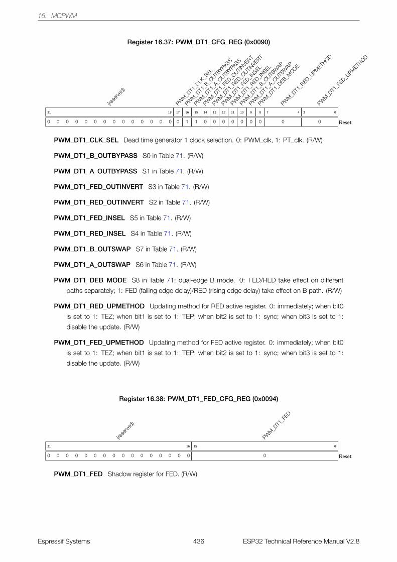
16. MCPWM
Register 16.37: PWM_DT1_CFG_REG (0x0090)
(rese
rved)
0 0 0 0 0 0 0 0 0 0 0 0 0 0
31 18
PWM
_DT1
_CLK
_SEL
0
17
PWM
_DT1
_B_O
UTBYPA
SS
1
16
PWM
_DT1
_A_O
UTBYPA
SS
1
15
PWM
_DT1
_FED_O
UTINVERT
0
14
PWM
_DT1
_RED_O
UTINVERT
0
13
PWM
_DT1
_FED_IN
SEL
0
12
PWM
_DT1
_RED_IN
SEL
0
11
PWM
_DT1
_B_O
UTSW
AP
0
10
PWM
_DT1
_A_O
UTSW
AP
0
9
PWM
_DT1
_DEB_M
ODE
0
8
PWM
_DT1
_RED_U
PMETH
OD
0
7 4
PWM
_DT1
_FED_U
PMETH
OD
0
3 0
Reset
PWM_DT1_CLK_SEL Dead time generator 1 clock selection. 0: PWM_clk, 1: PT_clk. (R/W)
PWM_DT1_B_OUTBYPASS S0 in Table 71. (R/W)
PWM_DT1_A_OUTBYPASS S1 in Table 71. (R/W)
PWM_DT1_FED_OUTINVERT S3 in Table 71. (R/W)
PWM_DT1_RED_OUTINVERT S2 in Table 71. (R/W)
PWM_DT1_FED_INSEL S5 in Table 71. (R/W)
PWM_DT1_RED_INSEL S4 in Table 71. (R/W)
PWM_DT1_B_OUTSWAP S7 in Table 71. (R/W)
PWM_DT1_A_OUTSWAP S6 in Table 71. (R/W)
PWM_DT1_DEB_MODE S8 in Table 71; dual-edge B mode. 0: FED/RED take effect on different
paths separately; 1: FED (falling edge delay)/RED (rising edge delay) take effect on B path. (R/W)
PWM_DT1_RED_UPMETHOD Updating method for RED active register. 0: immediately; when bit0
is set to 1: TEZ; when bit1 is set to 1: TEP; when bit2 is set to 1: sync; when bit3 is set to 1:
disable the update. (R/W)
PWM_DT1_FED_UPMETHOD Updating method for FED active register. 0: immediately; when bit0
is set to 1: TEZ; when bit1 is set to 1: TEP; when bit2 is set to 1: sync; when bit3 is set to 1:
disable the update. (R/W)
Register 16.38: PWM_DT1_FED_CFG_REG (0x0094)
(rese
rved)
0 0 0 0 0 0 0 0 0 0 0 0 0 0 0 0
31 16
PWM
_DT1
_FED
0
15 0
Reset
PWM_DT1_FED Shadow register for FED. (R/W)
Espressif Systems 436 ESP32 Technical Reference Manual V2.8
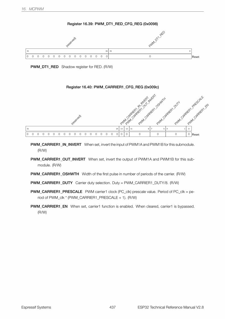
16. MCPWM
Register 16.39: PWM_DT1_RED_CFG_REG (0x0098)
(rese
rved)
0 0 0 0 0 0 0 0 0 0 0 0 0 0 0 0
31 16
PWM
_DT1
_RED
0
15 0
Reset
PWM_DT1_RED Shadow register for RED. (R/W)
Register 16.40: PWM_CARRIER1_CFG_REG (0x009c)
(rese
rved)
0 0 0 0 0 0 0 0 0 0 0 0 0 0 0 0 0 0
31 14
PWM
_CARRIER1_
IN_IN
VERT
0
13
PWM
_CARRIER1_
OUT_IN
VERT
0
12
PWM
_CARRIER1_
OSHWTH
0
11 8
PWM
_CARRIER1_
DUTY
0
7 5
PWM
_CARRIER1_
PRESCALE
0
4 1
PWM
_CARRIER1_
EN
0
0
Reset
PWM_CARRIER1_IN_INVERT When set, invert the input of PWM1A and PWM1B for this submodule.
(R/W)
PWM_CARRIER1_OUT_INVERT When set, invert the output of PWM1A and PWM1B for this sub-
module. (R/W)
PWM_CARRIER1_OSHWTH Width of the first pulse in number of periods of the carrier. (R/W)
PWM_CARRIER1_DUTY Carrier duty selection. Duty = PWM_CARRIER1_DUTY/8. (R/W)
PWM_CARRIER1_PRESCALE PWM carrier1 clock (PC_clk) prescale value. Period of PC_clk = pe-
riod of PWM_clk * (PWM_CARRIER1_PRESCALE + 1). (R/W)
PWM_CARRIER1_EN When set, carrier1 function is enabled. When cleared, carrier1 is bypassed.
(R/W)
Espressif Systems 437 ESP32 Technical Reference Manual V2.8
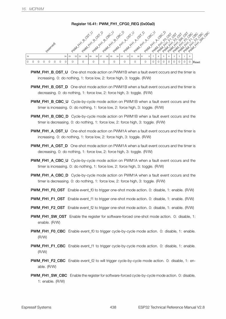
16. MCPWM
Register 16.41: PWM_FH1_CFG0_REG (0x00a0)
(rese
rved)
0 0 0 0 0 0 0 0
31 24
PWM
_FH1_
B_OST_
U
0
23 22
PWM
_FH1_
B_OST_
D
0
21 20
PWM
_FH1_
B_CBC_U
0
19 18
PWM
_FH1_
B_CBC_D
0
17 16
PWM
_FH1_
A_OST_
U
0
15 14
PWM
_FH1_
A_OST_
D
0
13 12
PWM
_FH1_
A_CBC_U
0
11 10
PWM
_FH1_
A_CBC_D
0
9 8
PWM
_FH1_
F0_O
ST
0
7
PWM
_FH1_
F1_O
ST
0
6
PWM
_FH1_
F2_O
ST
0
5
PWM
_FH1_
SW_O
ST
0
4
PWM
_FH1_
F0_C
BC
0
3
PWM
_FH1_
F1_C
BC
0
2
PWM
_FH1_
F2_C
BC
0
1
PWM
_FH1_
SW_C
BC
0
0
Reset
PWM_FH1_B_OST_U One-shot mode action on PWM1B when a fault event occurs and the timer is
increasing. 0: do nothing, 1: force low, 2: force high, 3: toggle. (R/W)
PWM_FH1_B_OST_D One-shot mode action on PWM1B when a fault event occurs and the timer is
decreasing. 0: do nothing, 1: force low, 2: force high, 3: toggle. (R/W)
PWM_FH1_B_CBC_U Cycle-by-cycle mode action on PWM1B when a fault event occurs and the
timer is increasing. 0: do nothing, 1: force low, 2: force high, 3: toggle. (R/W)
PWM_FH1_B_CBC_D Cycle-by-cycle mode action on PWM1B when a fault event occurs and the
timer is decreasing. 0: do nothing, 1: force low, 2: force high, 3: toggle. (R/W)
PWM_FH1_A_OST_U One-shot mode action on PWM1A when a fault event occurs and the timer is
increasing. 0: do nothing, 1: force low, 2: force high, 3: toggle. (R/W)
PWM_FH1_A_OST_D One-shot mode action on PWM1A when a fault event occurs and the timer is
decreasing. 0: do nothing, 1: force low, 2: force high, 3: toggle. (R/W)
PWM_FH1_A_CBC_U Cycle-by-cycle mode action on PWM1A when a fault event occurs and the
timer is increasing. 0: do nothing, 1: force low, 2: force high, 3: toggle. (R/W)
PWM_FH1_A_CBC_D Cycle-by-cycle mode action on PWM1A when a fault event occurs and the
timer is decreasing. 0: do nothing, 1: force low, 2: force high, 3: toggle. (R/W)
PWM_FH1_F0_OST Enable event_f0 to trigger one-shot mode action. 0: disable, 1: enable. (R/W)
PWM_FH1_F1_OST Enable event_f1 to trigger one-shot mode action. 0: disable, 1: enable. (R/W)
PWM_FH1_F2_OST Enable event_f2 to trigger one-shot mode action. 0: disable, 1: enable. (R/W)
PWM_FH1_SW_OST Enable the register for software-forced one-shot mode action. 0: disable, 1:
enable. (R/W)
PWM_FH1_F0_CBC Enable event_f0 to trigger cycle-by-cycle mode action. 0: disable, 1: enable.
(R/W)
PWM_FH1_F1_CBC Enable event_f1 to trigger cycle-by-cycle mode action. 0: disable, 1: enable.
(R/W)
PWM_FH1_F2_CBC Enable event_f2 to will trigger cycle-by-cycle mode action. 0: disable, 1: en-
able. (R/W)
PWM_FH1_SW_CBC Enable the register for software-forced cycle-by-cycle mode action. 0: disable,
1: enable. (R/W)
Espressif Systems 438 ESP32 Technical Reference Manual V2.8

16. MCPWM
Register 16.42: PWM_FH1_CFG1_REG (0x00a4)
(rese
rved)
0 0 0 0 0 0 0 0 0 0 0 0 0 0 0 0 0 0 0 0 0 0 0 0 0 0 0
31 5
PWM
_FH1_
FORCE_O
ST
0
4
PWM
_FH1_
FORCE_C
BC
0
3
PWM
_FH1_
CBCPULSE
0
2 1
PWM
_FH1_
CLR_O
ST
0
0
Reset
PWM_FH1_FORCE_OST A toggle (software negation of this bit’s value) triggers a one-shot mode
action. (R/W)
PWM_FH1_FORCE_CBC A toggle triggers a cycle-by-cycle mode action. (R/W)
PWM_FH1_CBCPULSE The cycle-by-cycle mode action refresh moment selection. When bit0 is set
to 1: TEZ; when bit1 is set to 1: TEP. (R/W)
PWM_FH1_CLR_OST A toggle will clear on-going one-shot mode action. (R/W)
Register 16.43: PWM_FH1_STATUS_REG (0x00a8)
(rese
rved)
0 0 0 0 0 0 0 0 0 0 0 0 0 0 0 0 0 0 0 0 0 0 0 0 0 0 0 0 0 0
31 2
PWM
_FH1_
OST_ON
0
1
PWM
_FH1_
CBC_ON
0
0
Reset
PWM_FH1_OST_ON Set and reset by hardware. If set, a one-shot mode action is on-going. (RO)
PWM_FH1_CBC_ON Set and reset by hardware. If set, a cycle-by-cycle mode action is on-going.
(RO)
Espressif Systems 439 ESP32 Technical Reference Manual V2.8
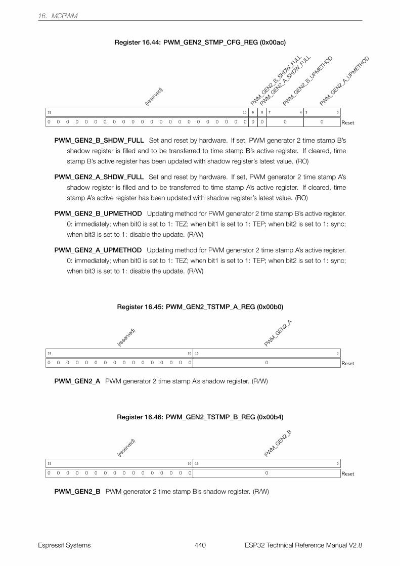
16. MCPWM
Register 16.44: PWM_GEN2_STMP_CFG_REG (0x00ac)
(rese
rved)
0 0 0 0 0 0 0 0 0 0 0 0 0 0 0 0 0 0 0 0 0 0
31 10
PWM
_GEN2_
B_SHDW
_FULL
0
9
PWM
_GEN2_
A_SHDW
_FULL
0
8
PWM
_GEN2_
B_UPM
ETHOD
0
7 4
PWM
_GEN2_
A_UPM
ETHOD
0
3 0
Reset
PWM_GEN2_B_SHDW_FULL Set and reset by hardware. If set, PWM generator 2 time stamp B’s
shadow register is filled and to be transferred to time stamp B’s active register. If cleared, time
stamp B’s active register has been updated with shadow register’s latest value. (RO)
PWM_GEN2_A_SHDW_FULL Set and reset by hardware. If set, PWM generator 2 time stamp A’s
shadow register is filled and to be transferred to time stamp A’s active register. If cleared, time
stamp A’s active register has been updated with shadow register’s latest value. (RO)
PWM_GEN2_B_UPMETHOD Updating method for PWM generator 2 time stamp B’s active register.
0: immediately; when bit0 is set to 1: TEZ; when bit1 is set to 1: TEP; when bit2 is set to 1: sync;
when bit3 is set to 1: disable the update. (R/W)
PWM_GEN2_A_UPMETHOD Updating method for PWM generator 2 time stamp A’s active register.
0: immediately; when bit0 is set to 1: TEZ; when bit1 is set to 1: TEP; when bit2 is set to 1: sync;
when bit3 is set to 1: disable the update. (R/W)
Register 16.45: PWM_GEN2_TSTMP_A_REG (0x00b0)
(rese
rved)
0 0 0 0 0 0 0 0 0 0 0 0 0 0 0 0
31 16
PWM
_GEN2_
A
0
15 0
Reset
PWM_GEN2_A PWM generator 2 time stamp A’s shadow register. (R/W)
Register 16.46: PWM_GEN2_TSTMP_B_REG (0x00b4)
(rese
rved)
0 0 0 0 0 0 0 0 0 0 0 0 0 0 0 0
31 16
PWM
_GEN2_
B
0
15 0
Reset
PWM_GEN2_B PWM generator 2 time stamp B’s shadow register. (R/W)
Espressif Systems 440 ESP32 Technical Reference Manual V2.8
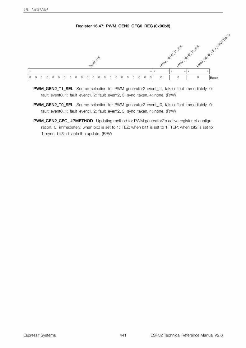
16. MCPWM
Register 16.47: PWM_GEN2_CFG0_REG (0x00b8)
(rese
rved)
0 0 0 0 0 0 0 0 0 0 0 0 0 0 0 0 0 0 0 0 0 0
31 10
PWM
_GEN2_
T1_S
EL
0
9 7
PWM
_GEN2_
T0_S
EL
0
6 4
PWM
_GEN2_
CFG_U
PMETH
OD
0
3 0
Reset
PWM_GEN2_T1_SEL Source selection for PWM generator2 event_t1, take effect immediately, 0:
fault_event0, 1: fault_event1, 2: fault_event2, 3: sync_taken, 4: none. (R/W)
PWM_GEN2_T0_SEL Source selection for PWM generator2 event_t0, take effect immediately, 0:
fault_event0, 1: fault_event1, 2: fault_event2, 3: sync_taken, 4: none. (R/W)
PWM_GEN2_CFG_UPMETHOD Updating method for PWM generator2’s active register of configu-
ration. 0: immediately; when bit0 is set to 1: TEZ; when bit1 is set to 1: TEP; when bit2 is set to
1: sync. bit3: disable the update. (R/W)
Espressif Systems 441 ESP32 Technical Reference Manual V2.8
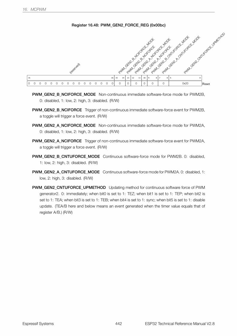
16. MCPWM
Register 16.48: PWM_GEN2_FORCE_REG (0x00bc)
(rese
rved)
0 0 0 0 0 0 0 0 0 0 0 0 0 0 0 0
31 16
PWM
_GEN2_
B_NCIFO
RCE_MODE
0
15 14
PWM
_GEN2_
B_NCIFO
RCE
0
13
PWM
_GEN2_
A_NCIFO
RCE_MODE
0
12 11
PWM
_GEN2_
A_NCIFO
RCE
0
10
PWM
_GEN2_
B_CNTU
FORCE_M
ODE
0
9 8
PWM
_GEN2_
A_CNTU
FORCE_M
ODE
0
7 6
PWM
_GEN2_
CNTUFO
RCE_UPM
ETHOD
0x20
5 0
Reset
PWM_GEN2_B_NCIFORCE_MODE Non-continuous immediate software-force mode for PWM2B,
0: disabled, 1: low, 2: high, 3: disabled. (R/W)
PWM_GEN2_B_NCIFORCE Trigger of non-continuous immediate software-force event for PWM2B,
a toggle will trigger a force event. (R/W)
PWM_GEN2_A_NCIFORCE_MODE Non-continuous immediate software-force mode for PWM2A,
0: disabled, 1: low, 2: high, 3: disabled. (R/W)
PWM_GEN2_A_NCIFORCE Trigger of non-continuous immediate software-force event for PWM2A,
a toggle will trigger a force event. (R/W)
PWM_GEN2_B_CNTUFORCE_MODE Continuous software-force mode for PWM2B. 0: disabled,
1: low, 2: high, 3: disabled. (R/W)
PWM_GEN2_A_CNTUFORCE_MODE Continuous software-force mode for PWM2A. 0: disabled, 1:
low, 2: high, 3: disabled. (R/W)
PWM_GEN2_CNTUFORCE_UPMETHOD Updating method for continuous software force of PWM
generator2. 0: immediately; when bit0 is set to 1: TEZ; when bit1 is set to 1: TEP; when bit2 is
set to 1: TEA; when bit3 is set to 1: TEB; when bit4 is set to 1: sync; when bit5 is set to 1: disable
update. (TEA/B here and below means an event generated when the timer value equals that of
register A/B.) (R/W)
Espressif Systems 442 ESP32 Technical Reference Manual V2.8

16. MCPWM
Register 16.49: PWM_GEN2_A_REG (0x00c0)
(rese
rved)
0 0 0 0 0 0 0 0
31 24
PWM
_GEN2_
A_DT1
0
23 22
PWM
_GEN2_
A_DT0
0
21 20
PWM
_GEN2_
A_DTE
B
0
19 18
PWM
_GEN2_
A_DTE
A
0
17 16
PWM
_GEN2_
A_DTE
P
0
15 14
PWM
_GEN2_
A_DTE
Z
0
13 12
PWM
_GEN2_
A_UT1
0
11 10
PWM
_GEN2_
A_UT0
0
9 8
PWM
_GEN2_
A_UTE
B
0
7 6
PWM
_GEN2_
A_UTE
A
0
5 4
PWM
_GEN2_
A_UTE
P
0
3 2
PWM
_GEN2_
A_UTE
Z
0
1 0
Reset
PWM_GEN2_A_DT1 Action on PWM2A triggered by event_t1 when the timer decreases. 0: no
change, 1: low, 2: high, 3: toggle. (R/W)
PWM_GEN2_A_DT0 Action on PWM2A triggered by event_t0 when the timer decreases. (R/W)
PWM_GEN2_A_DTEB Action on PWM2A triggered by event TEB when the timer decreases. (R/W)
PWM_GEN2_A_DTEA Action on PWM2A triggered by event TEA when the timer decreases. (R/W)
PWM_GEN2_A_DTEP Action on PWM2A triggered by event TEP when the timer decreases. (R/W)
PWM_GEN2_A_DTEZ Action on PWM2A triggered by event TEZ when the timer decreases. (R/W)
PWM_GEN2_A_UT1 Action on PWM2A triggered by event_t1 when the timer increases. (R/W)
PWM_GEN2_A_UT0 Action on PWM2A triggered by event_t0 when the timer increases. (R/W)
PWM_GEN2_A_UTEB Action on PWM2A triggered by event TEB when the timer increases. (R/W)
PWM_GEN2_A_UTEA Action on PWM2A triggered by event TEA when the timer increases. (R/W)
PWM_GEN2_A_UTEP Action on PWM2A triggered by event TEP when the timer increases. (R/W)
PWM_GEN2_A_UTEZ Action on PWM2A triggered by event TEZ when the timer increases. (R/W)
Espressif Systems 443 ESP32 Technical Reference Manual V2.8

16. MCPWM
Register 16.50: PWM_GEN2_B_REG (0x00c4)
(rese
rved)
0 0 0 0 0 0 0 0
31 24
PWM
_GEN2_
B_DT1
0
23 22
PWM
_GEN2_
B_DT0
0
21 20
PWM
_GEN2_
B_DTE
B
0
19 18
PWM
_GEN2_
B_DTE
A
0
17 16
PWM
_GEN2_
B_DTE
P
0
15 14
PWM
_GEN2_
B_DTE
Z
0
13 12
PWM
_GEN2_
B_UT1
0
11 10
PWM
_GEN2_
B_UT0
0
9 8
PWM
_GEN2_
B_UTE
B
0
7 6
PWM
_GEN2_
B_UTE
A
0
5 4
PWM
_GEN2_
B_UTE
P
0
3 2
PWM
_GEN2_
B_UTE
Z
0
1 0
Reset
PWM_GEN2_B_DT1 Action on PWM2B triggered by event_t1 when the timer decreases. 0: no
change, 1: low, 2: high, 3: toggle. (R/W)
PWM_GEN2_B_DT0 Action on PWM2B triggered by event_t0 when the timer decreases. (R/W)
PWM_GEN2_B_DTEB Action on PWM2B triggered by event TEB when the timer decreases. (R/W)
PWM_GEN2_B_DTEA Action on PWM2B triggered by event TEA when the timer decreases. (R/W)
PWM_GEN2_B_DTEP Action on PWM2B triggered by event TEP when the timer decreases. (R/W)
PWM_GEN2_B_DTEZ Action on PWM2B triggered by event TEZ when the timer decreases. (R/W)
PWM_GEN2_B_UT1 Action on PWM2B triggered by event_t1 when the timer increases. (R/W)
PWM_GEN2_B_UT0 Action on PWM2B triggered by event_t0 when the timer increases. (R/W)
PWM_GEN2_B_UTEB Action on PWM2B triggered by event TEB when the timer increases. (R/W)
PWM_GEN2_B_UTEA Action on PWM2B triggered by event TEA when the timer increases. (R/W)
PWM_GEN2_B_UTEP Action on PWM2B triggered by event TEP when the timer increases. (R/W)
PWM_GEN2_B_UTEZ Action on PWM2B triggered by event TEZ when the timer increases. (R/W)
Espressif Systems 444 ESP32 Technical Reference Manual V2.8
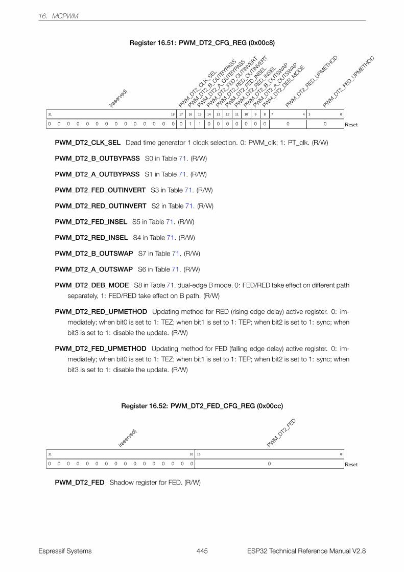
16. MCPWM
Register 16.51: PWM_DT2_CFG_REG (0x00c8)
(rese
rved)
0 0 0 0 0 0 0 0 0 0 0 0 0 0
31 18
PWM
_DT2
_CLK
_SEL
0
17
PWM
_DT2
_B_O
UTBYPA
SS
1
16
PWM
_DT2
_A_O
UTBYPA
SS
1
15
PWM
_DT2
_FED_O
UTINVERT
0
14
PWM
_DT2
_RED_O
UTINVERT
0
13
PWM
_DT2
_FED_IN
SEL
0
12
PWM
_DT2
_RED_IN
SEL
0
11
PWM
_DT2
_B_O
UTSW
AP
0
10
PWM
_DT2
_A_O
UTSW
AP
0
9
PWM
_DT2
_DEB_M
ODE
0
8
PWM
_DT2
_RED_U
PMETH
OD
0
7 4
PWM
_DT2
_FED_U
PMETH
OD
0
3 0
Reset
PWM_DT2_CLK_SEL Dead time generator 1 clock selection. 0: PWM_clk; 1: PT_clk. (R/W)
PWM_DT2_B_OUTBYPASS S0 in Table 71. (R/W)
PWM_DT2_A_OUTBYPASS S1 in Table 71. (R/W)
PWM_DT2_FED_OUTINVERT S3 in Table 71. (R/W)
PWM_DT2_RED_OUTINVERT S2 in Table 71. (R/W)
PWM_DT2_FED_INSEL S5 in Table 71. (R/W)
PWM_DT2_RED_INSEL S4 in Table 71. (R/W)
PWM_DT2_B_OUTSWAP S7 in Table 71. (R/W)
PWM_DT2_A_OUTSWAP S6 in Table 71. (R/W)
PWM_DT2_DEB_MODE S8 in Table 71, dual-edge B mode, 0: FED/RED take effect on different path
separately, 1: FED/RED take effect on B path. (R/W)
PWM_DT2_RED_UPMETHOD Updating method for RED (rising edge delay) active register. 0: im-
mediately; when bit0 is set to 1: TEZ; when bit1 is set to 1: TEP; when bit2 is set to 1: sync; when
bit3 is set to 1: disable the update. (R/W)
PWM_DT2_FED_UPMETHOD Updating method for FED (falling edge delay) active register. 0: im-
mediately; when bit0 is set to 1: TEZ; when bit1 is set to 1: TEP; when bit2 is set to 1: sync; when
bit3 is set to 1: disable the update. (R/W)
Register 16.52: PWM_DT2_FED_CFG_REG (0x00cc)
(rese
rved)
0 0 0 0 0 0 0 0 0 0 0 0 0 0 0 0
31 16
PWM
_DT2
_FED
0
15 0
Reset
PWM_DT2_FED Shadow register for FED. (R/W)
Espressif Systems 445 ESP32 Technical Reference Manual V2.8

16. MCPWM
Register 16.53: PWM_DT2_RED_CFG_REG (0x00d0)
(rese
rved)
0 0 0 0 0 0 0 0 0 0 0 0 0 0 0 0
31 16
PWM
_DT2
_RED
0
15 0
Reset
PWM_DT2_RED Shadow register for RED. (R/W)
Register 16.54: PWM_CARRIER2_CFG_REG (0x00d4)
(rese
rved)
0 0 0 0 0 0 0 0 0 0 0 0 0 0 0 0 0 0
31 14
PWM
_CARRIER2_
IN_IN
VERT
0
13
PWM
_CARRIER2_
OUT_IN
VERT
0
12
PWM
_CARRIER2_
OSHWTH
0
11 8
PWM
_CARRIER2_
DUTY
0
7 5
PWM
_CARRIER2_
PRESCALE
0
4 1
PWM
_CARRIER2_
EN
0
0
Reset
PWM_CARRIER2_IN_INVERT When set, invert the input of PWM2A and PWM2B for this submodule.
(R/W)
PWM_CARRIER2_OUT_INVERT When set, invert the output of PWM2A and PWM2B for this sub-
module. (R/W)
PWM_CARRIER2_OSHWTH Width of the first pulse in number of periods of the carrier. (R/W)
PWM_CARRIER2_DUTY Carrier duty selection. Duty = PWM_CARRIER2_DUTY / 8. (R/W)
PWM_CARRIER2_PRESCALE PWM carrier2 clock (PC_clk) prescale value. Period of PC_clk = pe-
riod of PWM_clk * (PWM_CARRIER2_PRESCALE + 1). (R/W)
PWM_CARRIER2_EN When set, carrier2 function is enabled. When cleared, carrier2 is bypassed.
(R/W)
Espressif Systems 446 ESP32 Technical Reference Manual V2.8
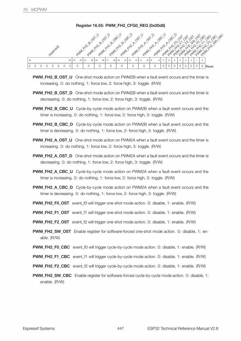
16. MCPWM
Register 16.55: PWM_FH2_CFG0_REG (0x00d8)
(rese
rved)
0 0 0 0 0 0 0 0
31 24
PWM
_FH2_
B_OST_
U
0
23 22
PWM
_FH2_
B_OST_
D
0
21 20
PWM
_FH2_
B_CBC_U
0
19 18
PWM
_FH2_
B_CBC_D
0
17 16
PWM
_FH2_
A_OST_
U
0
15 14
PWM
_FH2_
A_OST_
D
0
13 12
PWM
_FH2_
A_CBC_U
0
11 10
PWM
_FH2_
A_CBC_D
0
9 8
PWM
_FH2_
F0_O
ST
0
7
PWM
_FH2_
F1_O
ST
0
6
PWM
_FH2_
F2_O
ST
0
5
PWM
_FH2_
SW_O
ST
0
4
PWM
_FH2_
F0_C
BC
0
3
PWM
_FH2_
F1_C
BC
0
2
PWM
_FH2_
F2_C
BC
0
1
PWM
_FH2_
SW_C
BC
0
0
Reset
PWM_FH2_B_OST_U One-shot mode action on PWM2B when a fault event occurs and the timer is
increasing. 0: do nothing, 1: force low, 2: force high, 3: toggle. (R/W)
PWM_FH2_B_OST_D One-shot mode action on PWM2B when a fault event occurs and the timer is
decreasing. 0: do nothing, 1: force low, 2: force high, 3: toggle. (R/W)
PWM_FH2_B_CBC_U Cycle-by-cycle mode action on PWM2B when a fault event occurs and the
timer is increasing. 0: do nothing, 1: force low, 2: force high, 3: toggle. (R/W)
PWM_FH2_B_CBC_D Cycle-by-cycle mode action on PWM2B when a fault event occurs and the
timer is decreasing. 0: do nothing, 1: force low, 2: force high, 3: toggle. (R/W)
PWM_FH2_A_OST_U One-shot mode action on PWM2A when a fault event occurs and the timer is
increasing. 0: do nothing, 1: force low, 2: force high, 3: toggle. (R/W)
PWM_FH2_A_OST_D One-shot mode action on PWM2A when a fault event occurs and the timer is
decreasing. 0: do nothing, 1: force low, 2: force high, 3: toggle. (R/W)
PWM_FH2_A_CBC_U Cycle-by-cycle mode action on PWM2A when a fault event occurs and the
timer is increasing. 0: do nothing, 1: force low, 2: force high, 3: toggle. (R/W)
PWM_FH2_A_CBC_D Cycle-by-cycle mode action on PWM2A when a fault event occurs and the
timer is decreasing. 0: do nothing, 1: force low, 2: force high, 3: toggle. (R/W)
PWM_FH2_F0_OST event_f0 will trigger one-shot mode action. 0: disable, 1: enable. (R/W)
PWM_FH2_F1_OST event_f1 will trigger one-shot mode action. 0: disable, 1: enable. (R/W)
PWM_FH2_F2_OST event_f2 will trigger one-shot mode action. 0: disable, 1: enable. (R/W)
PWM_FH2_SW_OST Enable register for software-forced one-shot mode action. 0: disable, 1: en-
able. (R/W)
PWM_FH2_F0_CBC event_f0 will trigger cycle-by-cycle mode action. 0: disable, 1: enable. (R/W)
PWM_FH2_F1_CBC event_f1 will trigger cycle-by-cycle mode action. 0: disable, 1: enable. (R/W)
PWM_FH2_F2_CBC event_f2 will trigger cycle-by-cycle mode action. 0: disable, 1: enable. (R/W)
PWM_FH2_SW_CBC Enable register for software-forced cycle-by-cycle mode action. 0: disable, 1:
enable. (R/W)
Espressif Systems 447 ESP32 Technical Reference Manual V2.8

16. MCPWM
Register 16.56: PWM_FH2_CFG1_REG (0x00dc)
(rese
rved)
0 0 0 0 0 0 0 0 0 0 0 0 0 0 0 0 0 0 0 0 0 0 0 0 0 0 0
31 5
PWM
_FH2_
FORCE_O
ST
0
4
PWM
_FH2_
FORCE_C
BC
0
3
PWM
_FH2_
CBCPULSE
0
2 1
PWM
_FH2_
CLR_O
ST
0
0
Reset
PWM_FH2_FORCE_OST A toggle (software negation of this bit’s value) triggers a one-shot mode
action. (R/W)
PWM_FH2_FORCE_CBC A toggle triggers a cycle-by-cycle mode action. (R/W)
PWM_FH2_CBCPULSE The cycle-by-cycle mode action refresh moment selection. When bit0 is set
to 1: TEZ; when bit1 is set to 1:TEP. (R/W)
PWM_FH2_CLR_OST A toggle will clear on-going one-shot mode action. (R/W)
Register 16.57: PWM_FH2_STATUS_REG (0x00e0)
(rese
rved)
0 0 0 0 0 0 0 0 0 0 0 0 0 0 0 0 0 0 0 0 0 0 0 0 0 0 0 0 0 0
31 2
PWM
_FH2_
OST_ON
0
1
PWM
_FH2_
CBC_ON
0
0
Reset
PWM_FH2_OST_ON Set and reset by hardware. If set, a one-shot mode action is on-going. (RO)
PWM_FH2_CBC_ON Set and reset by hardware. If set, a cycle-by-cycle mode action is on-going.
(RO)
Espressif Systems 448 ESP32 Technical Reference Manual V2.8
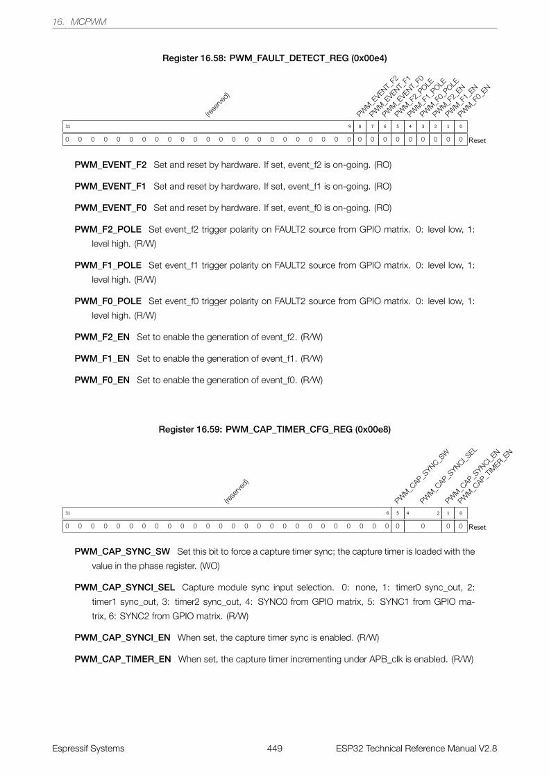
16. MCPWM
Register 16.58: PWM_FAULT_DETECT_REG (0x00e4)
(rese
rved)
0 0 0 0 0 0 0 0 0 0 0 0 0 0 0 0 0 0 0 0 0 0 0
31 9
PWM
_EVENT_
F2
0
8
PWM
_EVENT_
F1
0
7
PWM
_EVENT_
F0
0
6
PWM
_F2_
POLE
0
5
PWM
_F1_
POLE
0
4
PWM
_F0_
POLE
0
3
PWM
_F2_
EN
0
2
PWM
_F1_
EN
0
1
PWM
_F0_
EN
0
0
Reset
PWM_EVENT_F2 Set and reset by hardware. If set, event_f2 is on-going. (RO)
PWM_EVENT_F1 Set and reset by hardware. If set, event_f1 is on-going. (RO)
PWM_EVENT_F0 Set and reset by hardware. If set, event_f0 is on-going. (RO)
PWM_F2_POLE Set event_f2 trigger polarity on FAULT2 source from GPIO matrix. 0: level low, 1:
level high. (R/W)
PWM_F1_POLE Set event_f1 trigger polarity on FAULT2 source from GPIO matrix. 0: level low, 1:
level high. (R/W)
PWM_F0_POLE Set event_f0 trigger polarity on FAULT2 source from GPIO matrix. 0: level low, 1:
level high. (R/W)
PWM_F2_EN Set to enable the generation of event_f2. (R/W)
PWM_F1_EN Set to enable the generation of event_f1. (R/W)
PWM_F0_EN Set to enable the generation of event_f0. (R/W)
Register 16.59: PWM_CAP_TIMER_CFG_REG (0x00e8)
(rese
rved)
0 0 0 0 0 0 0 0 0 0 0 0 0 0 0 0 0 0 0 0 0 0 0 0 0 0
31 6
PWM
_CAP_S
YNC_SW
0
5
PWM
_CAP_S
YNCI_SEL
0
4 2
PWM
_CAP_S
YNCI_EN
0
1
PWM
_CAP_T
IMER_E
N
0
0
Reset
PWM_CAP_SYNC_SW Set this bit to force a capture timer sync; the capture timer is loaded with the
value in the phase register. (WO)
PWM_CAP_SYNCI_SEL Capture module sync input selection. 0: none, 1: timer0 sync_out, 2:
timer1 sync_out, 3: timer2 sync_out, 4: SYNC0 from GPIO matrix, 5: SYNC1 from GPIO ma-
trix, 6: SYNC2 from GPIO matrix. (R/W)
PWM_CAP_SYNCI_EN When set, the capture timer sync is enabled. (R/W)
PWM_CAP_TIMER_EN When set, the capture timer incrementing under APB_clk is enabled. (R/W)
Espressif Systems 449 ESP32 Technical Reference Manual V2.8
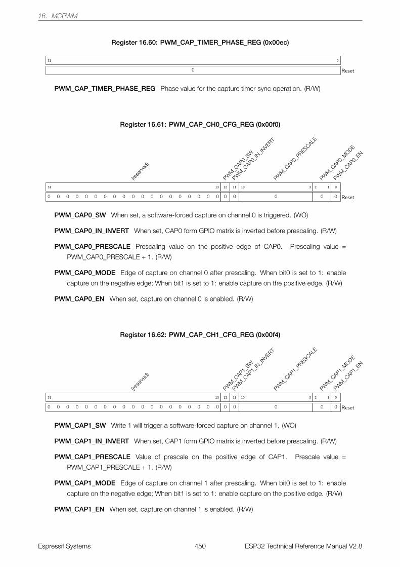
16. MCPWM
Register 16.60: PWM_CAP_TIMER_PHASE_REG (0x00ec)
0
31 0
Reset
PWM_CAP_TIMER_PHASE_REG Phase value for the capture timer sync operation. (R/W)
Register 16.61: PWM_CAP_CH0_CFG_REG (0x00f0)
(rese
rved)
0 0 0 0 0 0 0 0 0 0 0 0 0 0 0 0 0 0 0
31 13
PWM
_CAP0_
SW
0
12
PWM
_CAP0_
IN_IN
VERT
0
11
PWM
_CAP0_
PRESCALE
0
10 3
PWM
_CAP0_
MODE
0
2 1
PWM
_CAP0_
EN
0
0
Reset
PWM_CAP0_SW When set, a software-forced capture on channel 0 is triggered. (WO)
PWM_CAP0_IN_INVERT When set, CAP0 form GPIO matrix is inverted before prescaling. (R/W)
PWM_CAP0_PRESCALE Prescaling value on the positive edge of CAP0. Prescaling value =
PWM_CAP0_PRESCALE + 1. (R/W)
PWM_CAP0_MODE Edge of capture on channel 0 after prescaling. When bit0 is set to 1: enable
capture on the negative edge; When bit1 is set to 1: enable capture on the positive edge. (R/W)
PWM_CAP0_EN When set, capture on channel 0 is enabled. (R/W)
Register 16.62: PWM_CAP_CH1_CFG_REG (0x00f4)
(rese
rved)
0 0 0 0 0 0 0 0 0 0 0 0 0 0 0 0 0 0 0
31 13
PWM
_CAP1_
SW
0
12
PWM
_CAP1_
IN_IN
VERT
0
11
PWM
_CAP1_
PRESCALE
0
10 3
PWM
_CAP1_
MODE
0
2 1
PWM
_CAP1_
EN
0
0
Reset
PWM_CAP1_SW Write 1 will trigger a software-forced capture on channel 1. (WO)
PWM_CAP1_IN_INVERT When set, CAP1 form GPIO matrix is inverted before prescaling. (R/W)
PWM_CAP1_PRESCALE Value of prescale on the positive edge of CAP1. Prescale value =
PWM_CAP1_PRESCALE + 1. (R/W)
PWM_CAP1_MODE Edge of capture on channel 1 after prescaling. When bit0 is set to 1: enable
capture on the negative edge; When bit1 is set to 1: enable capture on the positive edge. (R/W)
PWM_CAP1_EN When set, capture on channel 1 is enabled. (R/W)
Espressif Systems 450 ESP32 Technical Reference Manual V2.8
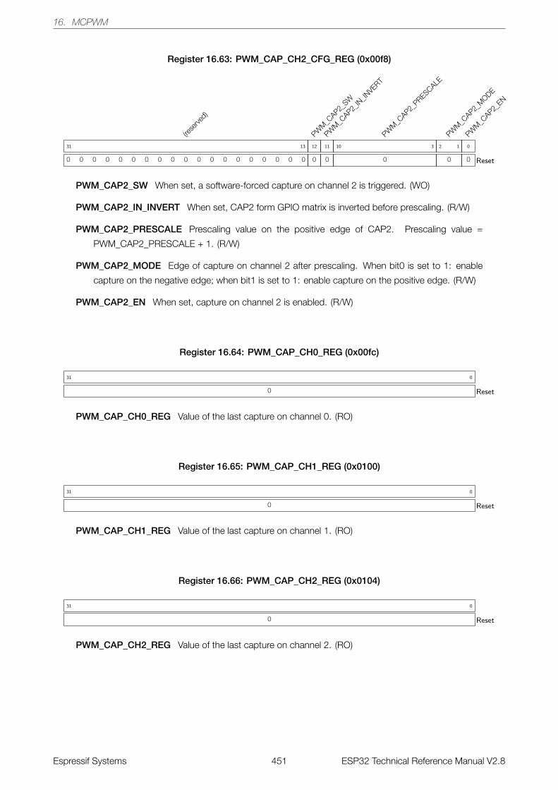
16. MCPWM
Register 16.63: PWM_CAP_CH2_CFG_REG (0x00f8)
(rese
rved)
0 0 0 0 0 0 0 0 0 0 0 0 0 0 0 0 0 0 0
31 13
PWM
_CAP2_
SW
0
12
PWM
_CAP2_
IN_IN
VERT
0
11
PWM
_CAP2_
PRESCALE
0
10 3
PWM
_CAP2_
MODE
0
2 1
PWM
_CAP2_
EN
0
0
Reset
PWM_CAP2_SW When set, a software-forced capture on channel 2 is triggered. (WO)
PWM_CAP2_IN_INVERT When set, CAP2 form GPIO matrix is inverted before prescaling. (R/W)
PWM_CAP2_PRESCALE Prescaling value on the positive edge of CAP2. Prescaling value =
PWM_CAP2_PRESCALE + 1. (R/W)
PWM_CAP2_MODE Edge of capture on channel 2 after prescaling. When bit0 is set to 1: enable
capture on the negative edge; when bit1 is set to 1: enable capture on the positive edge. (R/W)
PWM_CAP2_EN When set, capture on channel 2 is enabled. (R/W)
Register 16.64: PWM_CAP_CH0_REG (0x00fc)
0
31 0
Reset
PWM_CAP_CH0_REG Value of the last capture on channel 0. (RO)
Register 16.65: PWM_CAP_CH1_REG (0x0100)
0
31 0
Reset
PWM_CAP_CH1_REG Value of the last capture on channel 1. (RO)
Register 16.66: PWM_CAP_CH2_REG (0x0104)
0
31 0
Reset
PWM_CAP_CH2_REG Value of the last capture on channel 2. (RO)
Espressif Systems 451 ESP32 Technical Reference Manual V2.8
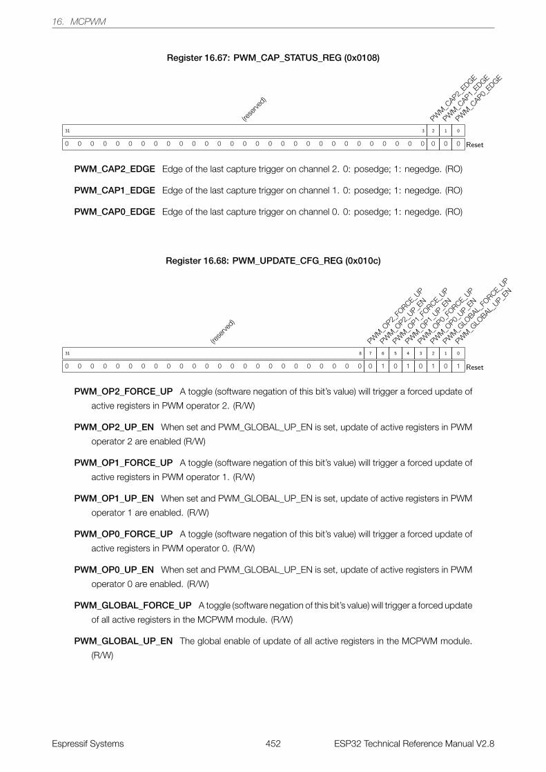
16. MCPWM
Register 16.67: PWM_CAP_STATUS_REG (0x0108)
(rese
rved)
0 0 0 0 0 0 0 0 0 0 0 0 0 0 0 0 0 0 0 0 0 0 0 0 0 0 0 0 0
31 3
PWM
_CAP2_
EDGE
0
2
PWM
_CAP1_
EDGE
0
1
PWM
_CAP0_
EDGE
0
0
Reset
PWM_CAP2_EDGE Edge of the last capture trigger on channel 2. 0: posedge; 1: negedge. (RO)
PWM_CAP1_EDGE Edge of the last capture trigger on channel 1. 0: posedge; 1: negedge. (RO)
PWM_CAP0_EDGE Edge of the last capture trigger on channel 0. 0: posedge; 1: negedge. (RO)
Register 16.68: PWM_UPDATE_CFG_REG (0x010c)
(rese
rved)
0 0 0 0 0 0 0 0 0 0 0 0 0 0 0 0 0 0 0 0 0 0 0 0
31 8
PWM
_OP2_
FORCE_U
P
0
7
PWM
_OP2_
UP_EN
1
6
PWM
_OP1_
FORCE_U
P
0
5
PWM
_OP1_
UP_EN
1
4
PWM
_OP0_
FORCE_U
P
0
3
PWM
_OP0_
UP_EN
1
2
PWM
_GLO
BAL_FO
RCE_UP
0
1
PWM
_GLO
BAL_UP_E
N
1
0
Reset
PWM_OP2_FORCE_UP A toggle (software negation of this bit’s value) will trigger a forced update of
active registers in PWM operator 2. (R/W)
PWM_OP2_UP_EN When set and PWM_GLOBAL_UP_EN is set, update of active registers in PWM
operator 2 are enabled (R/W)
PWM_OP1_FORCE_UP A toggle (software negation of this bit’s value) will trigger a forced update of
active registers in PWM operator 1. (R/W)
PWM_OP1_UP_EN When set and PWM_GLOBAL_UP_EN is set, update of active registers in PWM
operator 1 are enabled. (R/W)
PWM_OP0_FORCE_UP A toggle (software negation of this bit’s value) will trigger a forced update of
active registers in PWM operator 0. (R/W)
PWM_OP0_UP_EN When set and PWM_GLOBAL_UP_EN is set, update of active registers in PWM
operator 0 are enabled. (R/W)
PWM_GLOBAL_FORCE_UP A toggle (software negation of this bit’s value) will trigger a forced update
of all active registers in the MCPWM module. (R/W)
PWM_GLOBAL_UP_EN The global enable of update of all active registers in the MCPWM module.
(R/W)
Espressif Systems 452 ESP32 Technical Reference Manual V2.8
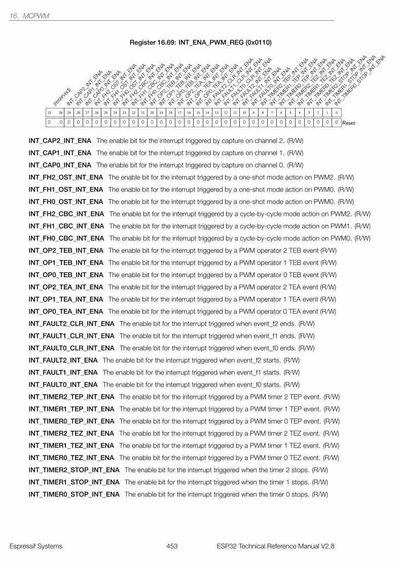
16. MCPWM
Register 16.69: INT_ENA_PWM_REG (0x0110)
(rese
rved)
0 0
31 30
INT_
CAP2_IN
T_ENA
0
29
INT_
CAP1_IN
T_ENA
0
28
INT_
CAP0_IN
T_ENA
0
27
INT_
FH2_
OST_IN
T_ENA
0
26
INT_
FH1_
OST_IN
T_ENA
0
25
INT_
FH0_
OST_IN
T_ENA
0
24
INT_
FH2_
CBC_INT_
ENA
0
23
INT_
FH1_
CBC_INT_
ENA
0
22
INT_
FH0_
CBC_INT_
ENA
0
21
INT_
OP2_TE
B_INT_
ENA
0
20
INT_
OP1_TE
B_INT_
ENA
0
19
INT_
OP0_TE
B_INT_
ENA
0
18
INT_
OP2_TE
A_INT_
ENA
0
17
INT_
OP1_TE
A_INT_
ENA
0
16
INT_
OP0_TE
A_INT_
ENA
0
15
INT_
FAULT
2_CLR
_INT_
ENA
0
14
INT_
FAULT
1_CLR
_INT_
ENA
0
13
INT_
FAULT
0_CLR
_INT_
ENA
0
12
INT_
FAULT
2_IN
T_ENA
0
11
INT_
FAULT
1_IN
T_ENA
0
10
INT_
FAULT
0_IN
T_ENA
0
9
INT_
TIMER2_
TEP_IN
T_ENA
0
8
INT_
TIMER1_
TEP_IN
T_ENA
0
7
INT_
TIMER0_
TEP_IN
T_ENA
0
6
INT_
TIMER2_
TEZ_
INT_
ENA
0
5
INT_
TIMER1_
TEZ_
INT_
ENA
0
4
INT_
TIMER0_
TEZ_
INT_
ENA
0
3
INT_
TIMER2_
STOP_IN
T_ENA
0
2
INT_
TIMER1_
STOP_IN
T_ENA
0
1
INT_
TIMER0_
STOP_IN
T_ENA
0
0
Reset
INT_CAP2_INT_ENA The enable bit for the interrupt triggered by capture on channel 2. (R/W)
INT_CAP1_INT_ENA The enable bit for the interrupt triggered by capture on channel 1. (R/W)
INT_CAP0_INT_ENA The enable bit for the interrupt triggered by capture on channel 0. (R/W)
INT_FH2_OST_INT_ENA The enable bit for the interrupt triggered by a one-shot mode action on PWM2. (R/W)
INT_FH1_OST_INT_ENA The enable bit for the interrupt triggered by a one-shot mode action on PWM0. (R/W)
INT_FH0_OST_INT_ENA The enable bit for the interrupt triggered by a one-shot mode action on PWM0. (R/W)
INT_FH2_CBC_INT_ENA The enable bit for the interrupt triggered by a cycle-by-cycle mode action on PWM2. (R/W)
INT_FH1_CBC_INT_ENA The enable bit for the interrupt triggered by a cycle-by-cycle mode action on PWM1. (R/W)
INT_FH0_CBC_INT_ENA The enable bit for the interrupt triggered by a cycle-by-cycle mode action on PWM0. (R/W)
INT_OP2_TEB_INT_ENA The enable bit for the interrupt triggered by a PWM operator 2 TEB event (R/W)
INT_OP1_TEB_INT_ENA The enable bit for the interrupt triggered by a PWM operator 1 TEB event (R/W)
INT_OP0_TEB_INT_ENA The enable bit for the interrupt triggered by a PWM operator 0 TEB event (R/W)
INT_OP2_TEA_INT_ENA The enable bit for the interrupt triggered by a PWM operator 2 TEA event (R/W)
INT_OP1_TEA_INT_ENA The enable bit for the interrupt triggered by a PWM operator 1 TEA event (R/W)
INT_OP0_TEA_INT_ENA The enable bit for the interrupt triggered by a PWM operator 0 TEA event (R/W)
INT_FAULT2_CLR_INT_ENA The enable bit for the interrupt triggered when event_f2 ends. (R/W)
INT_FAULT1_CLR_INT_ENA The enable bit for the interrupt triggered when event_f1 ends. (R/W)
INT_FAULT0_CLR_INT_ENA The enable bit for the interrupt triggered when event_f0 ends. (R/W)
INT_FAULT2_INT_ENA The enable bit for the interrupt triggered when event_f2 starts. (R/W)
INT_FAULT1_INT_ENA The enable bit for the interrupt triggered when event_f1 starts. (R/W)
INT_FAULT0_INT_ENA The enable bit for the interrupt triggered when event_f0 starts. (R/W)
INT_TIMER2_TEP_INT_ENA The enable bit for the interrupt triggered by a PWM timer 2 TEP event. (R/W)
INT_TIMER1_TEP_INT_ENA The enable bit for the interrupt triggered by a PWM timer 1 TEP event. (R/W)
INT_TIMER0_TEP_INT_ENA The enable bit for the interrupt triggered by a PWM timer 0 TEP event. (R/W)
INT_TIMER2_TEZ_INT_ENA The enable bit for the interrupt triggered by a PWM timer 2 TEZ event. (R/W)
INT_TIMER1_TEZ_INT_ENA The enable bit for the interrupt triggered by a PWM timer 1 TEZ event. (R/W)
INT_TIMER0_TEZ_INT_ENA The enable bit for the interrupt triggered by a PWM timer 0 TEZ event. (R/W)
INT_TIMER2_STOP_INT_ENA The enable bit for the interrupt triggered when the timer 2 stops. (R/W)
INT_TIMER1_STOP_INT_ENA The enable bit for the interrupt triggered when the timer 1 stops. (R/W)
INT_TIMER0_STOP_INT_ENA The enable bit for the interrupt triggered when the timer 0 stops. (R/W)
Espressif Systems 453 ESP32 Technical Reference Manual V2.8
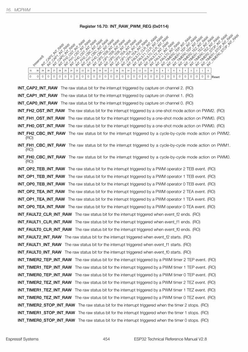
16. MCPWM
Register 16.70: INT_RAW_PWM_REG (0x0114)
(rese
rved)
0 0
31 30
INT_
CAP2_IN
T_RAW
0
29
INT_
CAP1_IN
T_RAW
0
28
INT_
CAP0_IN
T_RAW
0
27
INT_
FH2_
OST_IN
T_RAW
0
26
INT_
FH1_
OST_IN
T_RAW
0
25
INT_
FH0_
OST_IN
T_RAW
0
24
INT_
FH2_
CBC_INT_
RAW
0
23
INT_
FH1_
CBC_INT_
RAW
0
22
INT_
FH0_
CBC_INT_
RAW
0
21
INT_
OP2_TE
B_INT_
RAW
0
20
INT_
OP1_TE
B_INT_
RAW
0
19
INT_
OP0_TE
B_INT_
RAW
0
18
INT_
OP2_TE
A_INT_
RAW
0
17
INT_
OP1_TE
A_INT_
RAW
0
16
INT_
OP0_TE
A_INT_
RAW
0
15
INT_
FAULT
2_CLR
_INT_
RAW
0
14
INT_
FAULT
1_CLR
_INT_
RAW
0
13
INT_
FAULT
0_CLR
_INT_
RAW
0
12
INT_
FAULT
2_IN
T_RAW
0
11
INT_
FAULT
1_IN
T_RAW
0
10
INT_
FAULT
0_IN
T_RAW
0
9
INT_
TIMER2_
TEP_IN
T_RAW
0
8
INT_
TIMER1_
TEP_IN
T_RAW
0
7
INT_
TIMER0_
TEP_IN
T_RAW
0
6
INT_
TIMER2_
TEZ_
INT_
RAW
0
5
INT_
TIMER1_
TEZ_
INT_
RAW
0
4
INT_
TIMER0_
TEZ_
INT_
RAW
0
3
INT_
TIMER2_
STOP_IN
T_RAW
0
2
INT_
TIMER1_
STOP_IN
T_RAW
0
1
INT_
TIMER0_
STOP_IN
T_RAW
0
0
Reset
INT_CAP2_INT_RAW The raw status bit for the interrupt triggered by capture on channel 2. (RO)
INT_CAP1_INT_RAW The raw status bit for the interrupt triggered by capture on channel 1. (RO)
INT_CAP0_INT_RAW The raw status bit for the interrupt triggered by capture on channel 0. (RO)
INT_FH2_OST_INT_RAW The raw status bit for the interrupt triggered by a one-shot mode action on PWM2. (RO)
INT_FH1_OST_INT_RAW The raw status bit for the interrupt triggered by a one-shot mode action on PWM0. (RO)
INT_FH0_OST_INT_RAW The raw status bit for the interrupt triggered by a one-shot mode action on PWM0. (RO)
INT_FH2_CBC_INT_RAW The raw status bit for the interrupt triggered by a cycle-by-cycle mode action on PWM2.(RO)
INT_FH1_CBC_INT_RAW The raw status bit for the interrupt triggered by a cycle-by-cycle mode action on PWM1.(RO)
INT_FH0_CBC_INT_RAW The raw status bit for the interrupt triggered by a cycle-by-cycle mode action on PWM0.(RO)
INT_OP2_TEB_INT_RAW The raw status bit for the interrupt triggered by a PWM operator 2 TEB event. (RO)
INT_OP1_TEB_INT_RAW The raw status bit for the interrupt triggered by a PWM operator 1 TEB event. (RO)
INT_OP0_TEB_INT_RAW The raw status bit for the interrupt triggered by a PWM operator 0 TEB event. (RO)
INT_OP2_TEA_INT_RAW The raw status bit for the interrupt triggered by a PWM operator 2 TEA event. (RO)
INT_OP1_TEA_INT_RAW The raw status bit for the interrupt triggered by a PWM operator 1 TEA event. (RO)
INT_OP0_TEA_INT_RAW The raw status bit for the interrupt triggered by a PWM operator 0 TEA event. (RO)
INT_FAULT2_CLR_INT_RAW The raw status bit for the interrupt triggered when event_f2 ends. (RO)
INT_FAULT1_CLR_INT_RAW The raw status bit for the interrupt triggered when event_f1 ends. (RO)
INT_FAULT0_CLR_INT_RAW The raw status bit for the interrupt triggered when event_f0 ends. (RO)
INT_FAULT2_INT_RAW The raw status bit for the interrupt triggered when event_f2 starts. (RO)
INT_FAULT1_INT_RAW The raw status bit for the interrupt triggered when event_f1 starts. (RO)
INT_FAULT0_INT_RAW The raw status bit for the interrupt triggered when event_f0 starts. (RO)
INT_TIMER2_TEP_INT_RAW The raw status bit for the interrupt triggered by a PWM timer 2 TEP event. (RO)
INT_TIMER1_TEP_INT_RAW The raw status bit for the interrupt triggered by a PWM timer 1 TEP event. (RO)
INT_TIMER0_TEP_INT_RAW The raw status bit for the interrupt triggered by a PWM timer 0 TEP event. (RO)
INT_TIMER2_TEZ_INT_RAW The raw status bit for the interrupt triggered by a PWM timer 2 TEZ event. (RO)
INT_TIMER1_TEZ_INT_RAW The raw status bit for the interrupt triggered by a PWM timer 1 TEZ event. (RO)
INT_TIMER0_TEZ_INT_RAW The raw status bit for the interrupt triggered by a PWM timer 0 TEZ event. (RO)
INT_TIMER2_STOP_INT_RAW The raw status bit for the interrupt triggered when the timer 2 stops. (RO)
INT_TIMER1_STOP_INT_RAW The raw status bit for the interrupt triggered when the timer 1 stops. (RO)
INT_TIMER0_STOP_INT_RAW The raw status bit for the interrupt triggered when the timer 0 stops. (RO)
Espressif Systems 454 ESP32 Technical Reference Manual V2.8
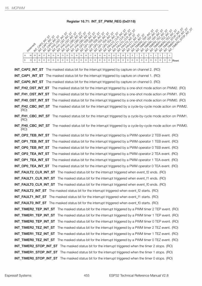
16. MCPWM
Register 16.71: INT_ST_PWM_REG (0x0118)
(rese
rved)
0 0
31 30
INT_
CAP2_IN
T_ST
0
29
INT_
CAP1_IN
T_ST
0
28
INT_
CAP0_IN
T_ST
0
27
INT_
FH2_
OST_IN
T_ST
0
26
INT_
FH1_
OST_IN
T_ST
0
25
INT_
FH0_
OST_IN
T_ST
0
24
INT_
FH2_
CBC_INT_
ST
0
23
INT_
FH1_
CBC_INT_
ST
0
22
INT_
FH0_
CBC_INT_
ST
0
21
INT_
OP2_TE
B_INT_
ST
0
20
INT_
OP1_TE
B_INT_
ST
0
19
INT_
OP0_TE
B_INT_
ST
0
18
INT_
OP2_TE
A_INT_
ST
0
17
INT_
OP1_TE
A_INT_
ST
0
16
INT_
OP0_TE
A_INT_
ST
0
15
INT_
FAULT
2_CLR
_INT_
ST
0
14
INT_
FAULT
1_CLR
_INT_
ST
0
13
INT_
FAULT
0_CLR
_INT_
ST
0
12
INT_
FAULT
2_IN
T_ST
0
11
INT_
FAULT
1_IN
T_ST
0
10
INT_
FAULT
0_IN
T_ST
0
9
INT_
TIMER2_
TEP_IN
T_ST
0
8
INT_
TIMER1_
TEP_IN
T_ST
0
7
INT_
TIMER0_
TEP_IN
T_ST
0
6
INT_
TIMER2_
TEZ_
INT_
ST
0
5
INT_
TIMER1_
TEZ_
INT_
ST
0
4
INT_
TIMER0_
TEZ_
INT_
ST
0
3
INT_
TIMER2_
STOP_IN
T_ST
0
2
INT_
TIMER1_
STOP_IN
T_ST
0
1
INT_
TIMER0_
STOP_IN
T_ST
0
0
Reset
INT_CAP2_INT_ST The masked status bit for the interrupt triggered by capture on channel 2. (RO)
INT_CAP1_INT_ST The masked status bit for the interrupt triggered by capture on channel 1. (RO)
INT_CAP0_INT_ST The masked status bit for the interrupt triggered by capture on channel 0. (RO)
INT_FH2_OST_INT_ST The masked status bit for the interrupt triggered by a one-shot mode action on PWM2. (RO)
INT_FH1_OST_INT_ST The masked status bit for the interrupt triggered by a one-shot mode action on PWM1. (RO)
INT_FH0_OST_INT_ST The masked status bit for the interrupt triggered by a one-shot mode action on PWM0. (RO)
INT_FH2_CBC_INT_ST The masked status bit for the interrupt triggered by a cycle-by-cycle mode action on PWM2.(RO)
INT_FH1_CBC_INT_ST The masked status bit for the interrupt triggered by a cycle-by-cycle mode action on PWM1.(RO)
INT_FH0_CBC_INT_ST The masked status bit for the interrupt triggered by a cycle-by-cycle mode action on PWM0.(RO)
INT_OP2_TEB_INT_ST The masked status bit for the interrupt triggered by a PWM operator 2 TEB event. (RO)
INT_OP1_TEB_INT_ST The masked status bit for the interrupt triggered by a PWM operator 1 TEB event. (RO)
INT_OP0_TEB_INT_ST The masked status bit for the interrupt triggered by a PWM operator 0 TEB event. (RO)
INT_OP2_TEA_INT_ST The masked status bit for the interrupt triggered by a PWM operator 2 TEA event. (RO)
INT_OP1_TEA_INT_ST The masked status bit for the interrupt triggered by a PWM operator 1 TEA event. (RO)
INT_OP0_TEA_INT_ST The masked status bit for the interrupt triggered by a PWM operator 0 TEA event. (RO)
INT_FAULT2_CLR_INT_ST The masked status bit for the interrupt triggered when event_f2 ends. (RO)
INT_FAULT1_CLR_INT_ST The masked status bit for the interrupt triggered when event_f1 ends. (RO)
INT_FAULT0_CLR_INT_ST The masked status bit for the interrupt triggered when event_f0 ends. (RO)
INT_FAULT2_INT_ST The masked status bit for the interrupt triggered when event_f2 starts. (RO)
INT_FAULT1_INT_ST The masked status bit for the interrupt triggered when event_f1 starts. (RO)
INT_FAULT0_INT_ST The masked status bit for the interrupt triggered when event_f0 starts. (RO)
INT_TIMER2_TEP_INT_ST The masked status bit for the interrupt triggered by a PWM timer 2 TEP event. (RO)
INT_TIMER1_TEP_INT_ST The masked status bit for the interrupt triggered by a PWM timer 1 TEP event. (RO)
INT_TIMER0_TEP_INT_ST The masked status bit for the interrupt triggered by a PWM timer 0 TEP event. (RO)
INT_TIMER2_TEZ_INT_ST The masked status bit for the interrupt triggered by a PWM timer 2 TEZ event. (RO)
INT_TIMER1_TEZ_INT_ST The masked status bit for the interrupt triggered by a PWM timer 1 TEZ event. (RO)
INT_TIMER0_TEZ_INT_ST The masked status bit for the interrupt triggered by a PWM timer 0 TEZ event. (RO)
INT_TIMER2_STOP_INT_ST The masked status bit for the interrupt triggered when the timer 2 stops. (RO)
INT_TIMER1_STOP_INT_ST The masked status bit for the interrupt triggered when the timer 1 stops. (RO)
INT_TIMER0_STOP_INT_ST The masked status bit for the interrupt triggered when the timer 0 stops. (RO)
Espressif Systems 455 ESP32 Technical Reference Manual V2.8
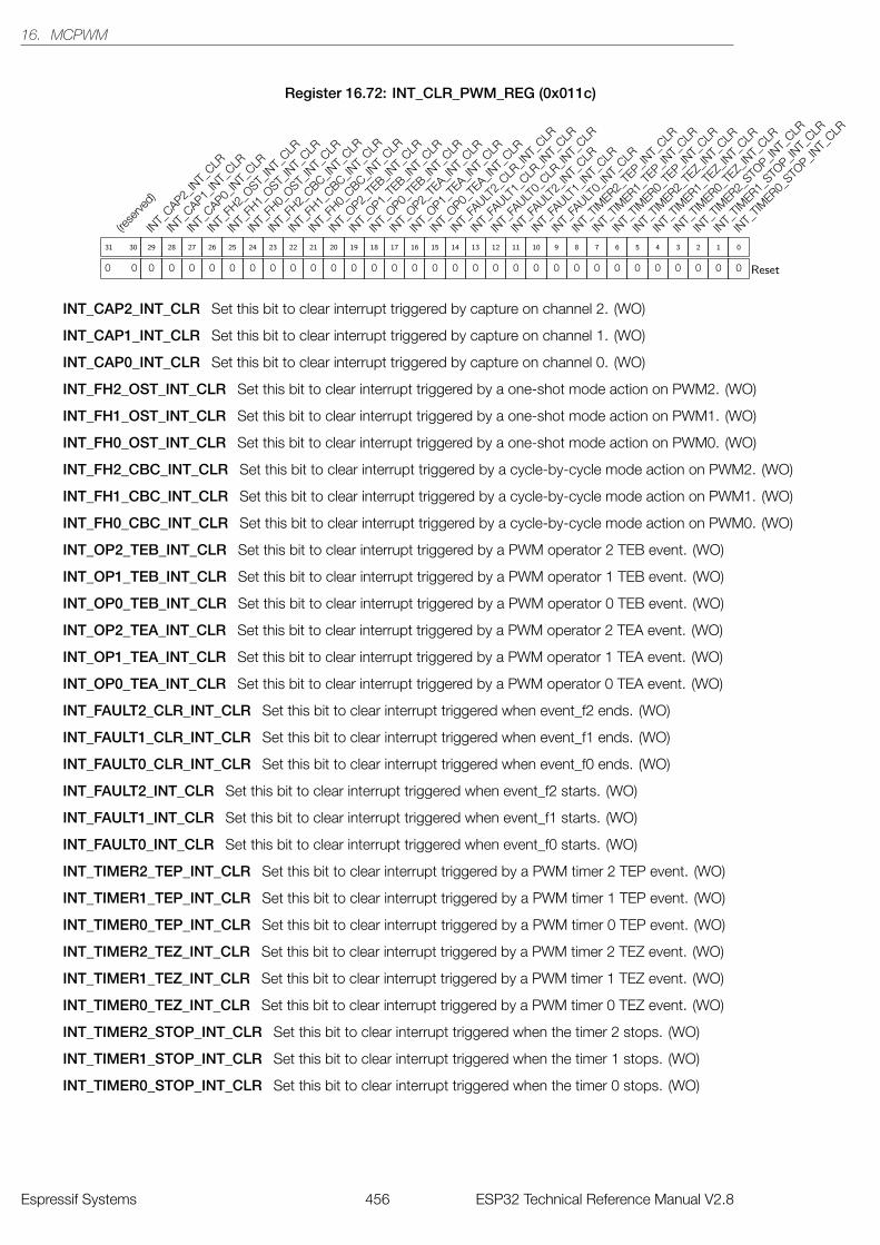
16. MCPWM
Register 16.72: INT_CLR_PWM_REG (0x011c)
(rese
rved)
0 0
31 30
INT_
CAP2_IN
T_CLR
0
29
INT_
CAP1_IN
T_CLR
0
28
INT_
CAP0_IN
T_CLR
0
27
INT_
FH2_
OST_IN
T_CLR
0
26
INT_
FH1_
OST_IN
T_CLR
0
25
INT_
FH0_
OST_IN
T_CLR
0
24
INT_
FH2_
CBC_INT_
CLR
0
23
INT_
FH1_
CBC_INT_
CLR
0
22
INT_
FH0_
CBC_INT_
CLR
0
21
INT_
OP2_TE
B_INT_
CLR
0
20
INT_
OP1_TE
B_INT_
CLR
0
19
INT_
OP0_TE
B_INT_
CLR
0
18
INT_
OP2_TE
A_INT_
CLR
0
17
INT_
OP1_TE
A_INT_
CLR
0
16
INT_
OP0_TE
A_INT_
CLR
0
15
INT_
FAULT
2_CLR
_INT_
CLR
0
14
INT_
FAULT
1_CLR
_INT_
CLR
0
13
INT_
FAULT
0_CLR
_INT_
CLR
0
12
INT_
FAULT
2_IN
T_CLR
0
11
INT_
FAULT
1_IN
T_CLR
0
10
INT_
FAULT
0_IN
T_CLR
0
9
INT_
TIMER2_
TEP_IN
T_CLR
0
8
INT_
TIMER1_
TEP_IN
T_CLR
0
7
INT_
TIMER0_
TEP_IN
T_CLR
0
6
INT_
TIMER2_
TEZ_
INT_
CLR
0
5
INT_
TIMER1_
TEZ_
INT_
CLR
0
4
INT_
TIMER0_
TEZ_
INT_
CLR
0
3
INT_
TIMER2_
STOP_IN
T_CLR
0
2
INT_
TIMER1_
STOP_IN
T_CLR
0
1
INT_
TIMER0_
STOP_IN
T_CLR
0
0
Reset
INT_CAP2_INT_CLR Set this bit to clear interrupt triggered by capture on channel 2. (WO)
INT_CAP1_INT_CLR Set this bit to clear interrupt triggered by capture on channel 1. (WO)
INT_CAP0_INT_CLR Set this bit to clear interrupt triggered by capture on channel 0. (WO)
INT_FH2_OST_INT_CLR Set this bit to clear interrupt triggered by a one-shot mode action on PWM2. (WO)
INT_FH1_OST_INT_CLR Set this bit to clear interrupt triggered by a one-shot mode action on PWM1. (WO)
INT_FH0_OST_INT_CLR Set this bit to clear interrupt triggered by a one-shot mode action on PWM0. (WO)
INT_FH2_CBC_INT_CLR Set this bit to clear interrupt triggered by a cycle-by-cycle mode action on PWM2. (WO)
INT_FH1_CBC_INT_CLR Set this bit to clear interrupt triggered by a cycle-by-cycle mode action on PWM1. (WO)
INT_FH0_CBC_INT_CLR Set this bit to clear interrupt triggered by a cycle-by-cycle mode action on PWM0. (WO)
INT_OP2_TEB_INT_CLR Set this bit to clear interrupt triggered by a PWM operator 2 TEB event. (WO)
INT_OP1_TEB_INT_CLR Set this bit to clear interrupt triggered by a PWM operator 1 TEB event. (WO)
INT_OP0_TEB_INT_CLR Set this bit to clear interrupt triggered by a PWM operator 0 TEB event. (WO)
INT_OP2_TEA_INT_CLR Set this bit to clear interrupt triggered by a PWM operator 2 TEA event. (WO)
INT_OP1_TEA_INT_CLR Set this bit to clear interrupt triggered by a PWM operator 1 TEA event. (WO)
INT_OP0_TEA_INT_CLR Set this bit to clear interrupt triggered by a PWM operator 0 TEA event. (WO)
INT_FAULT2_CLR_INT_CLR Set this bit to clear interrupt triggered when event_f2 ends. (WO)
INT_FAULT1_CLR_INT_CLR Set this bit to clear interrupt triggered when event_f1 ends. (WO)
INT_FAULT0_CLR_INT_CLR Set this bit to clear interrupt triggered when event_f0 ends. (WO)
INT_FAULT2_INT_CLR Set this bit to clear interrupt triggered when event_f2 starts. (WO)
INT_FAULT1_INT_CLR Set this bit to clear interrupt triggered when event_f1 starts. (WO)
INT_FAULT0_INT_CLR Set this bit to clear interrupt triggered when event_f0 starts. (WO)
INT_TIMER2_TEP_INT_CLR Set this bit to clear interrupt triggered by a PWM timer 2 TEP event. (WO)
INT_TIMER1_TEP_INT_CLR Set this bit to clear interrupt triggered by a PWM timer 1 TEP event. (WO)
INT_TIMER0_TEP_INT_CLR Set this bit to clear interrupt triggered by a PWM timer 0 TEP event. (WO)
INT_TIMER2_TEZ_INT_CLR Set this bit to clear interrupt triggered by a PWM timer 2 TEZ event. (WO)
INT_TIMER1_TEZ_INT_CLR Set this bit to clear interrupt triggered by a PWM timer 1 TEZ event. (WO)
INT_TIMER0_TEZ_INT_CLR Set this bit to clear interrupt triggered by a PWM timer 0 TEZ event. (WO)
INT_TIMER2_STOP_INT_CLR Set this bit to clear interrupt triggered when the timer 2 stops. (WO)
INT_TIMER1_STOP_INT_CLR Set this bit to clear interrupt triggered when the timer 1 stops. (WO)
INT_TIMER0_STOP_INT_CLR Set this bit to clear interrupt triggered when the timer 0 stops. (WO)
Espressif Systems 456 ESP32 Technical Reference Manual V2.8
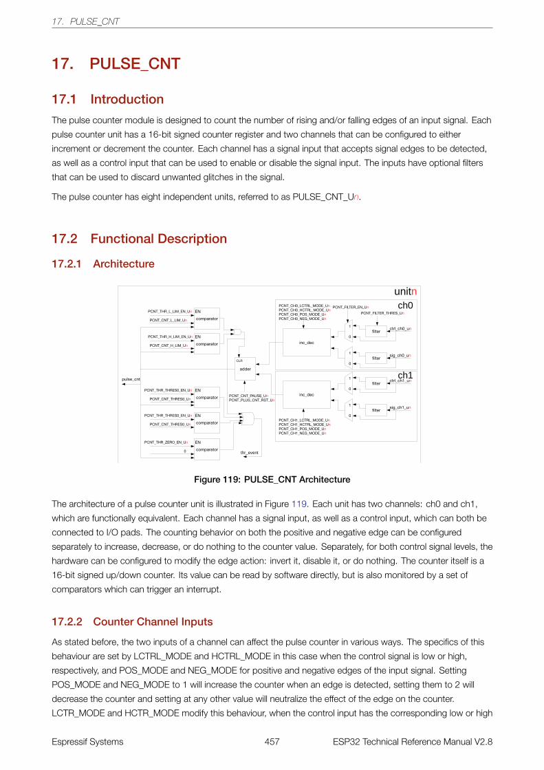
17. PULSE_CNT
17. PULSE_CNT
17.1 Introduction
The pulse counter module is designed to count the number of rising and/or falling edges of an input signal. Each
pulse counter unit has a 16-bit signed counter register and two channels that can be configured to either
increment or decrement the counter. Each channel has a signal input that accepts signal edges to be detected,
as well as a control input that can be used to enable or disable the signal input. The inputs have optional filters
that can be used to discard unwanted glitches in the signal.
The pulse counter has eight independent units, referred to as PULSE_CNT_Un.
17.2 Functional Description
17.2.1 Architecture
Figure 119: PULSE_CNT Architecture
The architecture of a pulse counter unit is illustrated in Figure 119. Each unit has two channels: ch0 and ch1,
which are functionally equivalent. Each channel has a signal input, as well as a control input, which can both be
connected to I/O pads. The counting behavior on both the positive and negative edge can be configured
separately to increase, decrease, or do nothing to the counter value. Separately, for both control signal levels, the
hardware can be configured to modify the edge action: invert it, disable it, or do nothing. The counter itself is a
16-bit signed up/down counter. Its value can be read by software directly, but is also monitored by a set of
comparators which can trigger an interrupt.
17.2.2 Counter Channel Inputs
As stated before, the two inputs of a channel can affect the pulse counter in various ways. The specifics of this
behaviour are set by LCTRL_MODE and HCTRL_MODE in this case when the control signal is low or high,
respectively, and POS_MODE and NEG_MODE for positive and negative edges of the input signal. Setting
POS_MODE and NEG_MODE to 1 will increase the counter when an edge is detected, setting them to 2 will
decrease the counter and setting at any other value will neutralize the effect of the edge on the counter.
LCTR_MODE and HCTR_MODE modify this behaviour, when the control input has the corresponding low or high
Espressif Systems 457 ESP32 Technical Reference Manual V2.8

17. PULSE_CNT
value: 0 does not modify the NEG_MODE and POS_MODE behaviour, 1 inverts it (setting
POS_MODE/NEG_MODE to increase the counter should now decrease the counter and vice versa) and any
other value disables counter effects for that signal level.
To summarize, a few examples have been considered. In this table, the effect on the counter for a rising edge is
shown for both a low and a high control signal, as well as various other configuration options. For clarity, a short
description in brackets is added after the values. Note: x denotes ’do not care’.
POS_ MODE LCTRL_ MODE HCTRL_ MODE sig l→h when ctrl=0 sig l→h when ctrl=1
1 (inc) 0 (-) 0 (-) Inc ctr Inc ctr
2 (dec) 0 (-) 0 (-) Dec ctr Dec ctr
0 (-) x x No action No action
1 (inc) 0 (-) 1 (inv) Inc ctr Dec ctr
1 (inc) 1 (inv) 0 (-) Dec ctr Inc ctr
2 (dec) 0 (-) 1 (inv) Dec ctr Inc ctr
1 (inc) 0 (-) 2 (dis) Inc ctr No action
1 (inc) 2 (dis) 0 (-) No action Inc ctr
This table is also valid for negative edges (sig h→l) on substituting NEG_MODE for POS_MODE.
Each pulse counter unit also features a filter on each of the four inputs, adding the option to ignore short glitches
in the signals. If a PCNT_FILTER_EN_Un can be set to filter the four input signals of the unit. If this filter is
enabled, any pulses shorter than REG_FILTER_THRES_Un number of APB_CLK clock cycles will be filtered out
and will have no effect on the counter. With the filter disabled, in theory infinitely small glitches could possibly
trigger pulse counter action. However, in practice the signal inputs are sampled on APB_CLK edges and even
with the filter disabled, pulse widths lasting shorter than one APB_CLK cycle may be missed.
Apart from the input channels, software also has some control over the counter. In particular, the counter value
can be frozen to the current value by configuring PCNT_CNT_PAUSE_Un. It can also be reset to 0 by configuring
PCNT_PULSE_CNT_RST_Un.
17.2.3 Watchpoints
The pulse counters have five watchpoints that share one interrupt. Interrupt generation can be enabled or
disabled for each individual watchpoint. The watchpoints are:
• Maximum count value: Triggered when PULSE_CNT >= PCNT_THR_H_LIM_Un. Additionally, this will reset
the counter to 0.
• Minimum count value: Triggered when PULSE_CNT <= PCNT_THR_L_LIM_Un. Additionally, this will reset
the counter to 0. This is most useful when PCNT_THR_L_LIM_Un is set to a negative number.
• Two threshold values: Triggered when PULSE_CNT = PCNT_THR_THRES0_Un or
PCNT_THR_THRES1_Un.
• Zero: Triggered when PULSE_CNT = 0.
Espressif Systems 458 ESP32 Technical Reference Manual V2.8
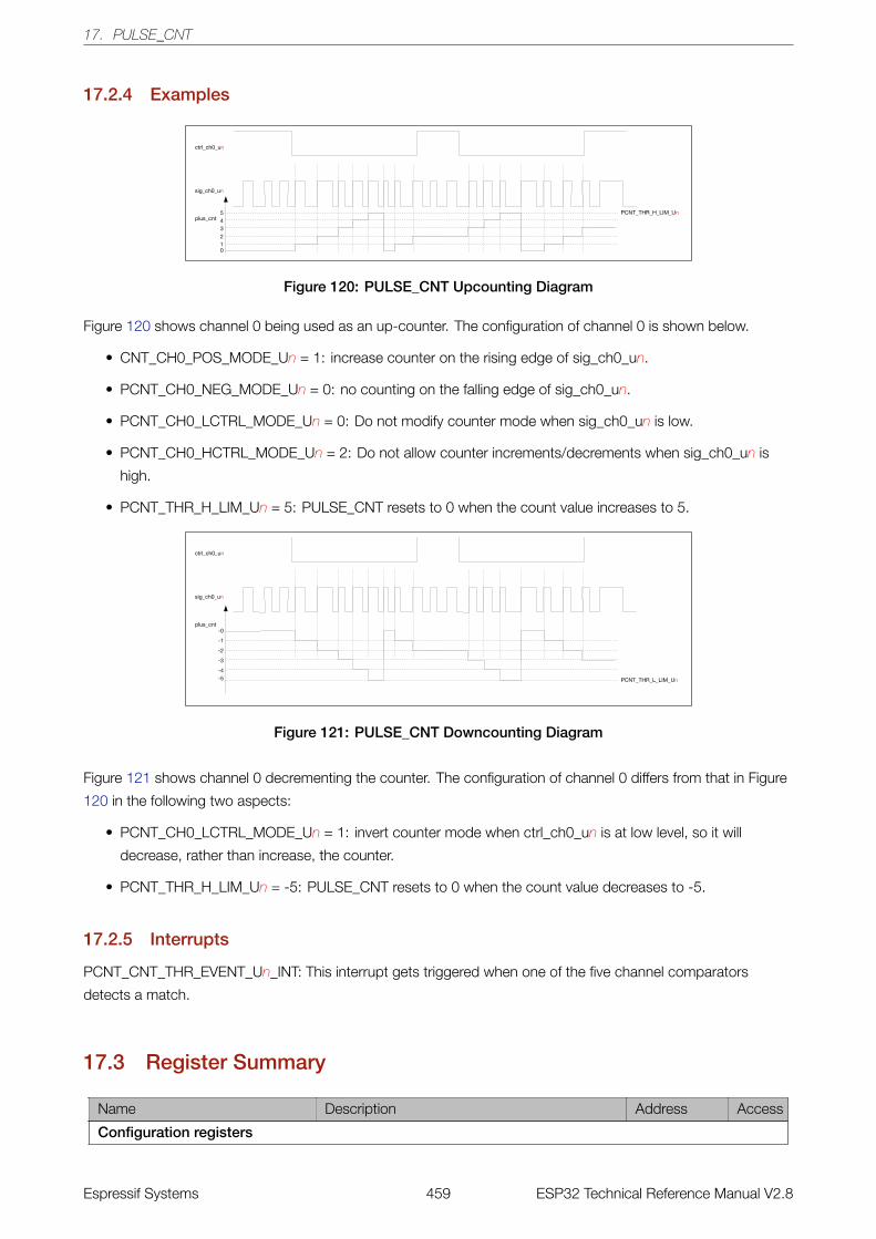
17. PULSE_CNT
17.2.4 Examples
Figure 120: PULSE_CNT Upcounting Diagram
Figure 120 shows channel 0 being used as an up-counter. The configuration of channel 0 is shown below.
• CNT_CH0_POS_MODE_Un = 1: increase counter on the rising edge of sig_ch0_un.
• PCNT_CH0_NEG_MODE_Un = 0: no counting on the falling edge of sig_ch0_un.
• PCNT_CH0_LCTRL_MODE_Un = 0: Do not modify counter mode when sig_ch0_un is low.
• PCNT_CH0_HCTRL_MODE_Un = 2: Do not allow counter increments/decrements when sig_ch0_un is
high.
• PCNT_THR_H_LIM_Un = 5: PULSE_CNT resets to 0 when the count value increases to 5.
Figure 121: PULSE_CNT Downcounting Diagram
Figure 121 shows channel 0 decrementing the counter. The configuration of channel 0 differs from that in Figure
120 in the following two aspects:
• PCNT_CH0_LCTRL_MODE_Un = 1: invert counter mode when ctrl_ch0_un is at low level, so it will
decrease, rather than increase, the counter.
• PCNT_THR_H_LIM_Un = -5: PULSE_CNT resets to 0 when the count value decreases to -5.
17.2.5 Interrupts
PCNT_CNT_THR_EVENT_Un_INT: This interrupt gets triggered when one of the five channel comparators
detects a match.
17.3 Register Summary
Name Description Address Access
Configuration registers
Espressif Systems 459 ESP32 Technical Reference Manual V2.8
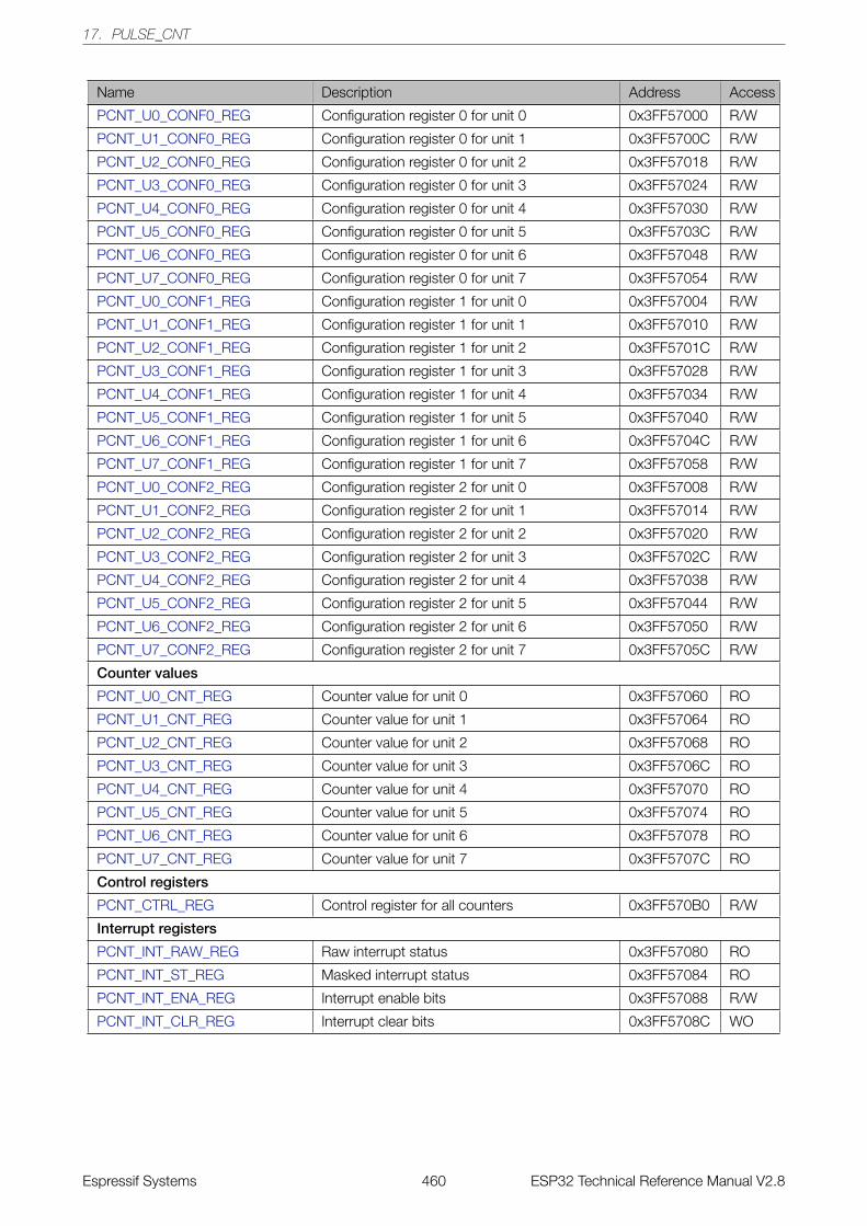
17. PULSE_CNT
Name Description Address Access
PCNT_U0_CONF0_REG Configuration register 0 for unit 0 0x3FF57000 R/W
PCNT_U1_CONF0_REG Configuration register 0 for unit 1 0x3FF5700C R/W
PCNT_U2_CONF0_REG Configuration register 0 for unit 2 0x3FF57018 R/W
PCNT_U3_CONF0_REG Configuration register 0 for unit 3 0x3FF57024 R/W
PCNT_U4_CONF0_REG Configuration register 0 for unit 4 0x3FF57030 R/W
PCNT_U5_CONF0_REG Configuration register 0 for unit 5 0x3FF5703C R/W
PCNT_U6_CONF0_REG Configuration register 0 for unit 6 0x3FF57048 R/W
PCNT_U7_CONF0_REG Configuration register 0 for unit 7 0x3FF57054 R/W
PCNT_U0_CONF1_REG Configuration register 1 for unit 0 0x3FF57004 R/W
PCNT_U1_CONF1_REG Configuration register 1 for unit 1 0x3FF57010 R/W
PCNT_U2_CONF1_REG Configuration register 1 for unit 2 0x3FF5701C R/W
PCNT_U3_CONF1_REG Configuration register 1 for unit 3 0x3FF57028 R/W
PCNT_U4_CONF1_REG Configuration register 1 for unit 4 0x3FF57034 R/W
PCNT_U5_CONF1_REG Configuration register 1 for unit 5 0x3FF57040 R/W
PCNT_U6_CONF1_REG Configuration register 1 for unit 6 0x3FF5704C R/W
PCNT_U7_CONF1_REG Configuration register 1 for unit 7 0x3FF57058 R/W
PCNT_U0_CONF2_REG Configuration register 2 for unit 0 0x3FF57008 R/W
PCNT_U1_CONF2_REG Configuration register 2 for unit 1 0x3FF57014 R/W
PCNT_U2_CONF2_REG Configuration register 2 for unit 2 0x3FF57020 R/W
PCNT_U3_CONF2_REG Configuration register 2 for unit 3 0x3FF5702C R/W
PCNT_U4_CONF2_REG Configuration register 2 for unit 4 0x3FF57038 R/W
PCNT_U5_CONF2_REG Configuration register 2 for unit 5 0x3FF57044 R/W
PCNT_U6_CONF2_REG Configuration register 2 for unit 6 0x3FF57050 R/W
PCNT_U7_CONF2_REG Configuration register 2 for unit 7 0x3FF5705C R/W
Counter values
PCNT_U0_CNT_REG Counter value for unit 0 0x3FF57060 RO
PCNT_U1_CNT_REG Counter value for unit 1 0x3FF57064 RO
PCNT_U2_CNT_REG Counter value for unit 2 0x3FF57068 RO
PCNT_U3_CNT_REG Counter value for unit 3 0x3FF5706C RO
PCNT_U4_CNT_REG Counter value for unit 4 0x3FF57070 RO
PCNT_U5_CNT_REG Counter value for unit 5 0x3FF57074 RO
PCNT_U6_CNT_REG Counter value for unit 6 0x3FF57078 RO
PCNT_U7_CNT_REG Counter value for unit 7 0x3FF5707C RO
Control registers
PCNT_CTRL_REG Control register for all counters 0x3FF570B0 R/W
Interrupt registers
PCNT_INT_RAW_REG Raw interrupt status 0x3FF57080 RO
PCNT_INT_ST_REG Masked interrupt status 0x3FF57084 RO
PCNT_INT_ENA_REG Interrupt enable bits 0x3FF57088 R/W
PCNT_INT_CLR_REG Interrupt clear bits 0x3FF5708C WO
Espressif Systems 460 ESP32 Technical Reference Manual V2.8
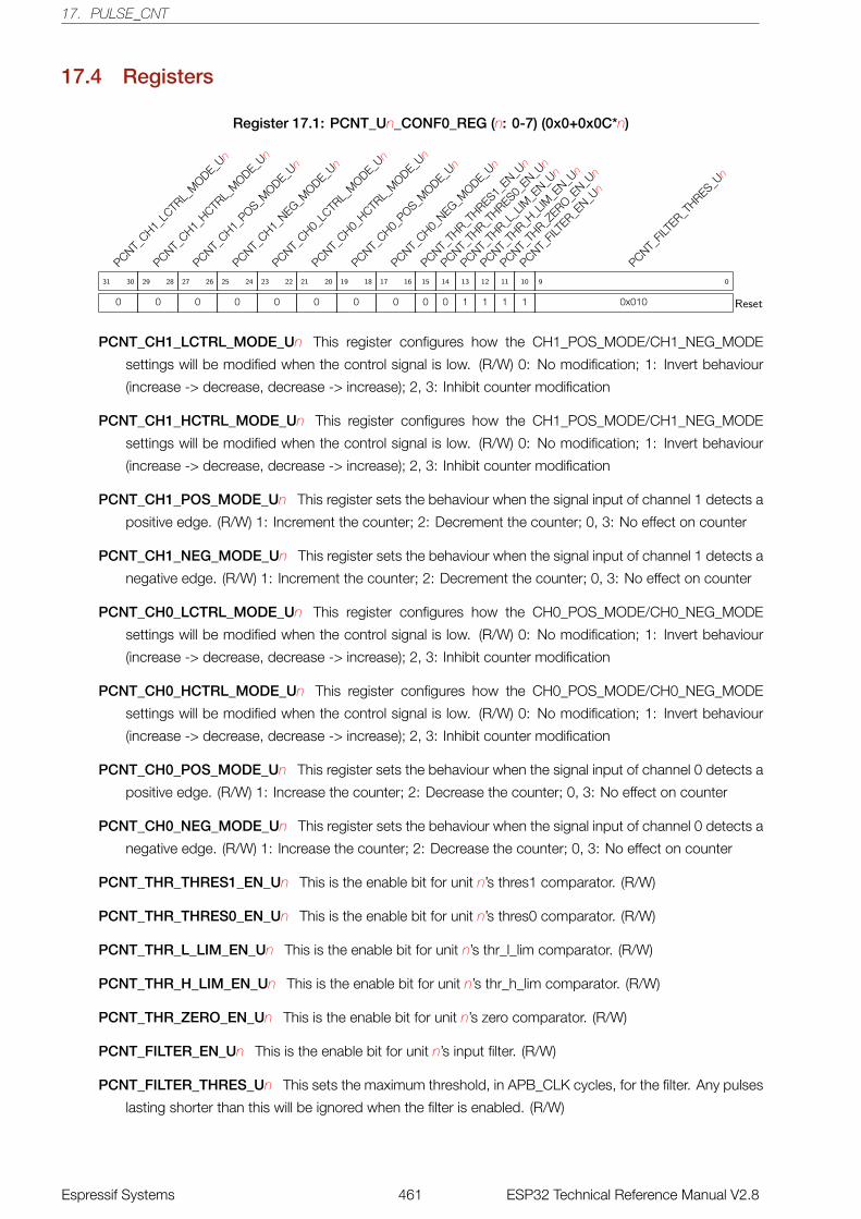
17. PULSE_CNT
17.4 Registers
Register 17.1: PCNT_Un_CONF0_REG (n: 0-7) (0x0+0x0C*n)
PCNT_CH1_
LCTR
L_M
ODE_Un
0
31 30
PCNT_CH1_
HCTRL_
MODE_U
n
0
29 28
PCNT_CH1_
POS_MODE_U
n
0
27 26
PCNT_CH1_
NEG_MODE_U
n
0
25 24
PCNT_CH0_
LCTR
L_M
ODE_Un
0
23 22
PCNT_CH0_
HCTRL_
MODE_U
n
0
21 20
PCNT_CH0_
POS_MODE_U
n
0
19 18
PCNT_CH0_
NEG_MODE_U
n
0
17 16
PCNT_TH
R_THRES1_
EN_Un
0
15
PCNT_TH
R_THRES0_
EN_Un
0
14
PCNT_TH
R_L_L
IM_E
N_Un
1
13
PCNT_TH
R_H_L
IM_E
N_Un
1
12
PCNT_TH
R_ZERO_E
N_Un
1
11
PCNT_FIL
TER_E
N_Un
1
10
PCNT_FIL
TER_T
HRES_Un
0x010
9 0
Reset
PCNT_CH1_LCTRL_MODE_Un This register configures how the CH1_POS_MODE/CH1_NEG_MODE
settings will be modified when the control signal is low. (R/W) 0: No modification; 1: Invert behaviour
(increase -> decrease, decrease -> increase); 2, 3: Inhibit counter modification
PCNT_CH1_HCTRL_MODE_Un This register configures how the CH1_POS_MODE/CH1_NEG_MODE
settings will be modified when the control signal is low. (R/W) 0: No modification; 1: Invert behaviour
(increase -> decrease, decrease -> increase); 2, 3: Inhibit counter modification
PCNT_CH1_POS_MODE_Un This register sets the behaviour when the signal input of channel 1 detects a
positive edge. (R/W) 1: Increment the counter; 2: Decrement the counter; 0, 3: No effect on counter
PCNT_CH1_NEG_MODE_Un This register sets the behaviour when the signal input of channel 1 detects a
negative edge. (R/W) 1: Increment the counter; 2: Decrement the counter; 0, 3: No effect on counter
PCNT_CH0_LCTRL_MODE_Un This register configures how the CH0_POS_MODE/CH0_NEG_MODE
settings will be modified when the control signal is low. (R/W) 0: No modification; 1: Invert behaviour
(increase -> decrease, decrease -> increase); 2, 3: Inhibit counter modification
PCNT_CH0_HCTRL_MODE_Un This register configures how the CH0_POS_MODE/CH0_NEG_MODE
settings will be modified when the control signal is low. (R/W) 0: No modification; 1: Invert behaviour
(increase -> decrease, decrease -> increase); 2, 3: Inhibit counter modification
PCNT_CH0_POS_MODE_Un This register sets the behaviour when the signal input of channel 0 detects a
positive edge. (R/W) 1: Increase the counter; 2: Decrease the counter; 0, 3: No effect on counter
PCNT_CH0_NEG_MODE_Un This register sets the behaviour when the signal input of channel 0 detects a
negative edge. (R/W) 1: Increase the counter; 2: Decrease the counter; 0, 3: No effect on counter
PCNT_THR_THRES1_EN_Un This is the enable bit for unit n’s thres1 comparator. (R/W)
PCNT_THR_THRES0_EN_Un This is the enable bit for unit n’s thres0 comparator. (R/W)
PCNT_THR_L_LIM_EN_Un This is the enable bit for unit n’s thr_l_lim comparator. (R/W)
PCNT_THR_H_LIM_EN_Un This is the enable bit for unit n’s thr_h_lim comparator. (R/W)
PCNT_THR_ZERO_EN_Un This is the enable bit for unit n’s zero comparator. (R/W)
PCNT_FILTER_EN_Un This is the enable bit for unit n’s input filter. (R/W)
PCNT_FILTER_THRES_Un This sets the maximum threshold, in APB_CLK cycles, for the filter. Any pulses
lasting shorter than this will be ignored when the filter is enabled. (R/W)
Espressif Systems 461 ESP32 Technical Reference Manual V2.8
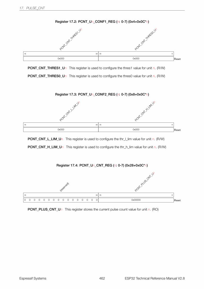
17. PULSE_CNT
Register 17.2: PCNT_Un_CONF1_REG (n: 0-7) (0x4+0x0C*n)
PCNT_CNT_
THRES1_
Un
0x000
31 16
PCNT_CNT_
THRES0_
Un
0x000
15 0
Reset
PCNT_CNT_THRES1_Un This register is used to configure the thres1 value for unit n. (R/W)
PCNT_CNT_THRES0_Un This register is used to configure the thres0 value for unit n. (R/W)
Register 17.3: PCNT_Un_CONF2_REG (n: 0-7) (0x8+0x0C*n)
PCNT_CNT_
L_LIM
_Un
0x000
31 16
PCNT_CNT_
H_LIM
_Un
0x000
15 0
Reset
PCNT_CNT_L_LIM_Un This register is used to configure the thr_l_lim value for unit n. (R/W)
PCNT_CNT_H_LIM_Un This register is used to configure the thr_h_lim value for unit n. (R/W)
Register 17.4: PCNT_Un_CNT_REG (n: 0-7) (0x28+0x0C*n)
(rese
rved)
0 0 0 0 0 0 0 0 0 0 0 0 0 0 0 0
31 16
PCNT_PLU
S_CNT_
Un
0x00000
15 0
Reset
PCNT_PLUS_CNT_Un This register stores the current pulse count value for unit n. (RO)
Espressif Systems 462 ESP32 Technical Reference Manual V2.8
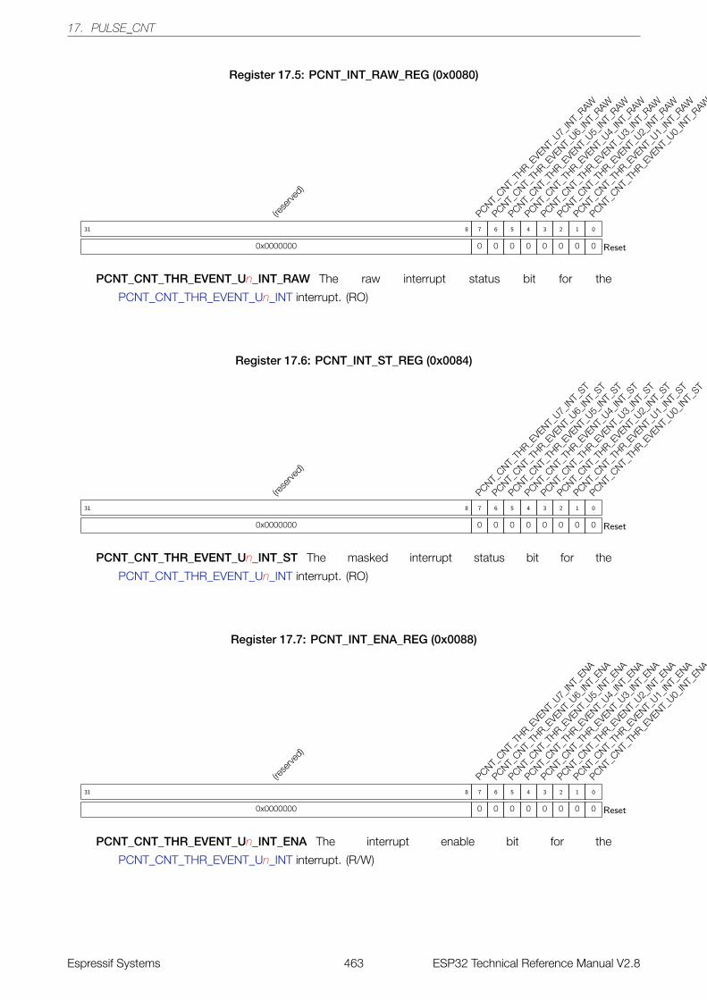
17. PULSE_CNT
Register 17.5: PCNT_INT_RAW_REG (0x0080)
(rese
rved)
0x0000000
31 8
PCNT_CNT_
THR_E
VENT_U7_
INT_
RAW
0
7
PCNT_CNT_
THR_E
VENT_U6_
INT_
RAW
0
6
PCNT_CNT_
THR_E
VENT_U5_
INT_
RAW
0
5
PCNT_CNT_
THR_E
VENT_U4_
INT_
RAW
0
4
PCNT_CNT_
THR_E
VENT_U3_
INT_
RAW
0
3
PCNT_CNT_
THR_E
VENT_U2_
INT_
RAW
0
2
PCNT_CNT_
THR_E
VENT_U1_
INT_
RAW
0
1
PCNT_CNT_
THR_E
VENT_U0_
INT_
RAW
0
0
Reset
PCNT_CNT_THR_EVENT_Un_INT_RAW The raw interrupt status bit for the
PCNT_CNT_THR_EVENT_Un_INT interrupt. (RO)
Register 17.6: PCNT_INT_ST_REG (0x0084)
(rese
rved)
0x0000000
31 8
PCNT_CNT_
THR_E
VENT_U7_
INT_
ST
0
7
PCNT_CNT_
THR_E
VENT_U6_
INT_
ST
0
6
PCNT_CNT_
THR_E
VENT_U5_
INT_
ST
0
5
PCNT_CNT_
THR_E
VENT_U4_
INT_
ST
0
4
PCNT_CNT_
THR_E
VENT_U3_
INT_
ST
0
3
PCNT_CNT_
THR_E
VENT_U2_
INT_
ST
0
2
PCNT_CNT_
THR_E
VENT_U1_
INT_
ST
0
1
PCNT_CNT_
THR_E
VENT_U0_
INT_
ST
0
0
Reset
PCNT_CNT_THR_EVENT_Un_INT_ST The masked interrupt status bit for the
PCNT_CNT_THR_EVENT_Un_INT interrupt. (RO)
Register 17.7: PCNT_INT_ENA_REG (0x0088)
(rese
rved)
0x0000000
31 8
PCNT_CNT_
THR_E
VENT_U7_
INT_
ENA
0
7
PCNT_CNT_
THR_E
VENT_U6_
INT_
ENA
0
6
PCNT_CNT_
THR_E
VENT_U5_
INT_
ENA
0
5
PCNT_CNT_
THR_E
VENT_U4_
INT_
ENA
0
4
PCNT_CNT_
THR_E
VENT_U3_
INT_
ENA
0
3
PCNT_CNT_
THR_E
VENT_U2_
INT_
ENA
0
2
PCNT_CNT_
THR_E
VENT_U1_
INT_
ENA
0
1
PCNT_CNT_
THR_E
VENT_U0_
INT_
ENA
0
0
Reset
PCNT_CNT_THR_EVENT_Un_INT_ENA The interrupt enable bit for the
PCNT_CNT_THR_EVENT_Un_INT interrupt. (R/W)
Espressif Systems 463 ESP32 Technical Reference Manual V2.8

17. PULSE_CNT
Register 17.8: PCNT_INT_CLR_REG (0x008c)
(rese
rved)
0x0000000
31 8
PCNT_CNT_
THR_E
VENT_U7_
INT_
CLR
0
7
PCNT_CNT_
THR_E
VENT_U6_
INT_
CLR
0
6
PCNT_CNT_
THR_E
VENT_U5_
INT_
CLR
0
5
PCNT_CNT_
THR_E
VENT_U4_
INT_
CLR
0
4
PCNT_CNT_
THR_E
VENT_U3_
INT_
CLR
0
3
PCNT_CNT_
THR_E
VENT_U2_
INT_
CLR
0
2
PCNT_CNT_
THR_E
VENT_U1_
INT_
CLR
0
1
PCNT_CNT_
THR_E
VENT_U0_
INT_
CLR
0
0
Reset
PCNT_CNT_THR_EVENT_Un_INT_CLR Set this bit to clear the PCNT_CNT_THR_EVENT_Un_INT
interrupt. (WO)
Register 17.9: PCNT_CTRL_REG (0x00b0)
(rese
rved)
0x0000
31 17
(rese
rved)
0
16
PCNT_CNT_
PAUSE_U
7
0
15
PCNT_PLU
S_CNT_
RST_U7
1
14
PCNT_CNT_
PAUSE_U
6
0
13
PCNT_PLU
S_CNT_
RST_U6
1
12
PCNT_CNT_
PAUSE_U
5
0
11
PCNT_PLU
S_CNT_
RST_U5
1
10
PCNT_CNT_
PAUSE_U
4
0
9
PCNT_PLU
S_CNT_
RST_U4
1
8
PCNT_CNT_
PAUSE_U
3
0
7
PCNT_PLU
S_CNT_
RST_U3
1
6
PCNT_CNT_
PAUSE_U
2
0
5
PCNT_PLU
S_CNT_
RST_U2
1
4
PCNT_CNT_
PAUSE_U
1
0
3
PCNT_PLU
S_CNT_
RST_U1
1
2
PCNT_CNT_
PAUSE_U
0
0
1
PCNT_PLU
S_CNT_
RST_U0
1
0
Reset
PCNT_CNT_PAUSE_Un Set this bit to freeze unit n’s counter. (R/W)
PCNT_PLUS_CNT_RST_Un Set this bit to clear unit n’s counter. (R/W)
Espressif Systems 464 ESP32 Technical Reference Manual V2.8
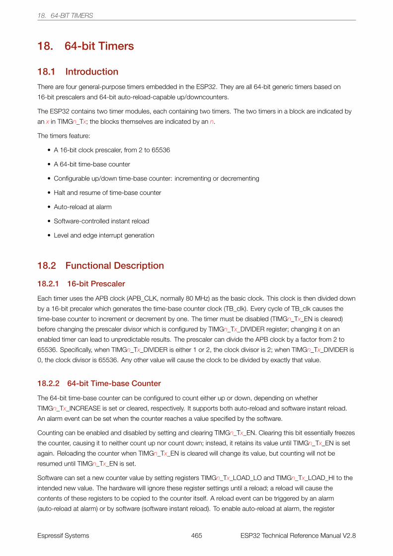
18. 64-BIT TIMERS
18. 64-bit Timers
18.1 Introduction
There are four general-purpose timers embedded in the ESP32. They are all 64-bit generic timers based on
16-bit prescalers and 64-bit auto-reload-capable up/downcounters.
The ESP32 contains two timer modules, each containing two timers. The two timers in a block are indicated by
an x in TIMGn_Tx; the blocks themselves are indicated by an n.
The timers feature:
• A 16-bit clock prescaler, from 2 to 65536
• A 64-bit time-base counter
• Configurable up/down time-base counter: incrementing or decrementing
• Halt and resume of time-base counter
• Auto-reload at alarm
• Software-controlled instant reload
• Level and edge interrupt generation
18.2 Functional Description
18.2.1 16-bit Prescaler
Each timer uses the APB clock (APB_CLK, normally 80 MHz) as the basic clock. This clock is then divided down
by a 16-bit precaler which generates the time-base counter clock (TB_clk). Every cycle of TB_clk causes the
time-base counter to increment or decrement by one. The timer must be disabled (TIMGn_Tx_EN is cleared)
before changing the prescaler divisor which is configured by TIMGn_Tx_DIVIDER register; changing it on an
enabled timer can lead to unpredictable results. The prescaler can divide the APB clock by a factor from 2 to
65536. Specifically, when TIMGn_Tx_DIVIDER is either 1 or 2, the clock divisor is 2; when TIMGn_Tx_DIVIDER is
0, the clock divisor is 65536. Any other value will cause the clock to be divided by exactly that value.
18.2.2 64-bit Time-base Counter
The 64-bit time-base counter can be configured to count either up or down, depending on whether
TIMGn_Tx_INCREASE is set or cleared, respectively. It supports both auto-reload and software instant reload.
An alarm event can be set when the counter reaches a value specified by the software.
Counting can be enabled and disabled by setting and clearing TIMGn_Tx_EN. Clearing this bit essentially freezes
the counter, causing it to neither count up nor count down; instead, it retains its value until TIMGn_Tx_EN is set
again. Reloading the counter when TIMGn_Tx_EN is cleared will change its value, but counting will not be
resumed until TIMGn_Tx_EN is set.
Software can set a new counter value by setting registers TIMGn_Tx_LOAD_LO and TIMGn_Tx_LOAD_HI to the
intended new value. The hardware will ignore these register settings until a reload; a reload will cause the
contents of these registers to be copied to the counter itself. A reload event can be triggered by an alarm
(auto-reload at alarm) or by software (software instant reload). To enable auto-reload at alarm, the register
Espressif Systems 465 ESP32 Technical Reference Manual V2.8
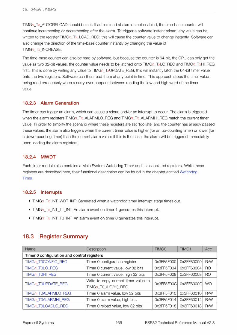
18. 64-BIT TIMERS
TIMGn_Tx_AUTORELOAD should be set. If auto-reload at alarm is not enabled, the time-base counter will
continue incrementing or decrementing after the alarm. To trigger a software instant reload, any value can be
written to the register TIMGn_Tx_LOAD_REG; this will cause the counter value to change instantly. Software can
also change the direction of the time-base counter instantly by changing the value of
TIMGn_Tx_INCREASE.
The time-base counter can also be read by software, but because the counter is 64-bit, the CPU can only get the
value as two 32-bit values, the counter value needs to be latched onto TIMGn_TxLO_REG and TIMGn_TxHI_REG
first. This is done by writing any value to TIMGn_TxUPDATE_REG; this will instantly latch the 64-bit timer value
onto the two registers. Software can then read them at any point in time. This approach stops the timer value
being read erroneously when a carry-over happens between reading the low and high word of the timer
value.
18.2.3 Alarm Generation
The timer can trigger an alarm, which can cause a reload and/or an interrupt to occur. The alarm is triggered
when the alarm registers TIMGn_Tx_ALARMLO_REG and TIMGn_Tx_ALARMHI_REG match the current timer
value. In order to simplify the scenario where these registers are set ’too late’ and the counter has already passed
these values, the alarm also triggers when the current timer value is higher (for an up-counting timer) or lower (for
a down-counting timer) than the current alarm value: if this is the case, the alarm will be triggered immediately
upon loading the alarm registers.
18.2.4 MWDT
Each timer module also contains a Main System Watchdog Timer and its associated registers. While these
registers are described here, their functional description can be found in the chapter entitled Watchdog
Timer.
18.2.5 Interrupts
• TIMGn_Tx_INT_WDT_INT: Generated when a watchdog timer interrupt stage times out.
• TIMGn_Tx_INT_T1_INT: An alarm event on timer 1 generates this interrupt.
• TIMGn_Tx_INT_T0_INT: An alarm event on timer 0 generates this interrupt.
18.3 Register Summary
Name Description TIMG0 TIMG1 Acc
Timer 0 configuration and control registers
TIMGn_T0CONFIG_REG Timer 0 configuration register 0x3FF5F000 0x3FF60000 R/W
TIMGn_T0LO_REG Timer 0 current value, low 32 bits 0x3FF5F004 0x3FF60004 RO
TIMGn_T0HI_REG Timer 0 current value, high 32 bits 0x3FF5F008 0x3FF60008 RO
TIMGn_T0UPDATE_REGWrite to copy current timer value to
TIMGn_T0_(LO/HI)_REG0x3FF5F00C 0x3FF6000C WO
TIMGn_T0ALARMLO_REG Timer 0 alarm value, low 32 bits 0x3FF5F010 0x3FF60010 R/W
TIMGn_T0ALARMHI_REG Timer 0 alarm value, high bits 0x3FF5F014 0x3FF60014 R/W
TIMGn_T0LOADLO_REG Timer 0 reload value, low 32 bits 0x3FF5F018 0x3FF60018 R/W
Espressif Systems 466 ESP32 Technical Reference Manual V2.8
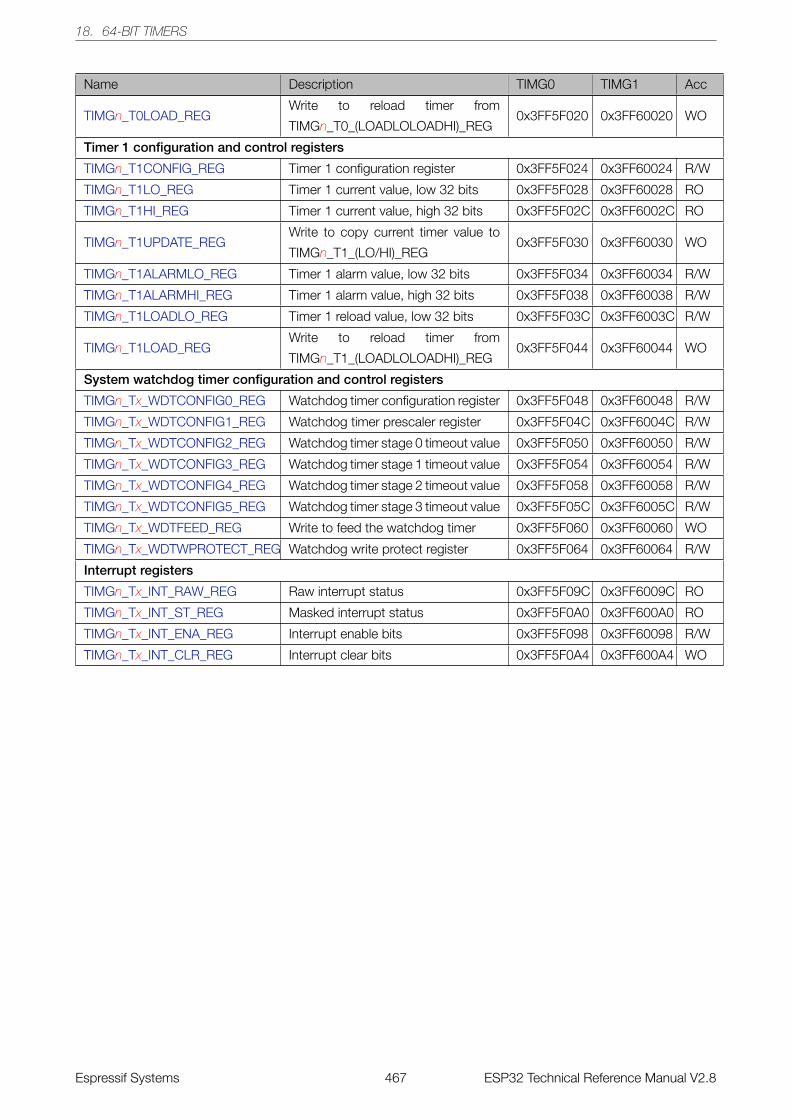
18. 64-BIT TIMERS
Name Description TIMG0 TIMG1 Acc
TIMGn_T0LOAD_REGWrite to reload timer from
TIMGn_T0_(LOADLOLOADHI)_REG0x3FF5F020 0x3FF60020 WO
Timer 1 configuration and control registers
TIMGn_T1CONFIG_REG Timer 1 configuration register 0x3FF5F024 0x3FF60024 R/W
TIMGn_T1LO_REG Timer 1 current value, low 32 bits 0x3FF5F028 0x3FF60028 RO
TIMGn_T1HI_REG Timer 1 current value, high 32 bits 0x3FF5F02C 0x3FF6002C RO
TIMGn_T1UPDATE_REGWrite to copy current timer value to
TIMGn_T1_(LO/HI)_REG0x3FF5F030 0x3FF60030 WO
TIMGn_T1ALARMLO_REG Timer 1 alarm value, low 32 bits 0x3FF5F034 0x3FF60034 R/W
TIMGn_T1ALARMHI_REG Timer 1 alarm value, high 32 bits 0x3FF5F038 0x3FF60038 R/W
TIMGn_T1LOADLO_REG Timer 1 reload value, low 32 bits 0x3FF5F03C 0x3FF6003C R/W
TIMGn_T1LOAD_REGWrite to reload timer from
TIMGn_T1_(LOADLOLOADHI)_REG0x3FF5F044 0x3FF60044 WO
System watchdog timer configuration and control registers
TIMGn_Tx_WDTCONFIG0_REG Watchdog timer configuration register 0x3FF5F048 0x3FF60048 R/W
TIMGn_Tx_WDTCONFIG1_REG Watchdog timer prescaler register 0x3FF5F04C 0x3FF6004C R/W
TIMGn_Tx_WDTCONFIG2_REG Watchdog timer stage 0 timeout value 0x3FF5F050 0x3FF60050 R/W
TIMGn_Tx_WDTCONFIG3_REG Watchdog timer stage 1 timeout value 0x3FF5F054 0x3FF60054 R/W
TIMGn_Tx_WDTCONFIG4_REG Watchdog timer stage 2 timeout value 0x3FF5F058 0x3FF60058 R/W
TIMGn_Tx_WDTCONFIG5_REG Watchdog timer stage 3 timeout value 0x3FF5F05C 0x3FF6005C R/W
TIMGn_Tx_WDTFEED_REG Write to feed the watchdog timer 0x3FF5F060 0x3FF60060 WO
TIMGn_Tx_WDTWPROTECT_REG Watchdog write protect register 0x3FF5F064 0x3FF60064 R/W
Interrupt registers
TIMGn_Tx_INT_RAW_REG Raw interrupt status 0x3FF5F09C 0x3FF6009C RO
TIMGn_Tx_INT_ST_REG Masked interrupt status 0x3FF5F0A0 0x3FF600A0 RO
TIMGn_Tx_INT_ENA_REG Interrupt enable bits 0x3FF5F098 0x3FF60098 R/W
TIMGn_Tx_INT_CLR_REG Interrupt clear bits 0x3FF5F0A4 0x3FF600A4 WO
Espressif Systems 467 ESP32 Technical Reference Manual V2.8
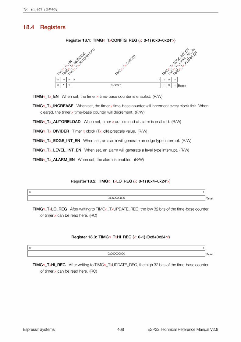
18. 64-BIT TIMERS
18.4 Registers
Register 18.1: TIMGn_TxCONFIG_REG (x: 0-1) (0x0+0x24*x)
TIMGn
_Tx_
EN
0
31
TIMGn
_Tx_
INCREASE
1
30
TIMGn
_Tx_
AUTORELO
AD
1
29
TIMGn
_Tx_
DIVIDER
0x00001
28 13
TIMGn
_Tx_
EDGE_INT_
EN
0
12
TIMGn
_Tx_
LEVEL_
INT_
EN
0
11
TIMGn
_Tx_
ALARM
_EN
0
10
Reset
TIMGn_Tx_EN When set, the timer x time-base counter is enabled. (R/W)
TIMGn_Tx_INCREASE When set, the timer x time-base counter will increment every clock tick. When
cleared, the timer x time-base counter will decrement. (R/W)
TIMGn_Tx_AUTORELOAD When set, timer x auto-reload at alarm is enabled. (R/W)
TIMGn_Tx_DIVIDER Timer x clock (Tx_clk) prescale value. (R/W)
TIMGn_Tx_EDGE_INT_EN When set, an alarm will generate an edge type interrupt. (R/W)
TIMGn_Tx_LEVEL_INT_EN When set, an alarm will generate a level type interrupt. (R/W)
TIMGn_Tx_ALARM_EN When set, the alarm is enabled. (R/W)
Register 18.2: TIMGn_TxLO_REG (x: 0-1) (0x4+0x24*x)
0x000000000
31 0
Reset
TIMGn_TxLO_REG After writing to TIMGn_TxUPDATE_REG, the low 32 bits of the time-base counter
of timer x can be read here. (RO)
Register 18.3: TIMGn_TxHI_REG (x: 0-1) (0x8+0x24*x)
0x000000000
31 0
Reset
TIMGn_TxHI_REG After writing to TIMGn_TxUPDATE_REG, the high 32 bits of the time-base counter
of timer x can be read here. (RO)
Espressif Systems 468 ESP32 Technical Reference Manual V2.8
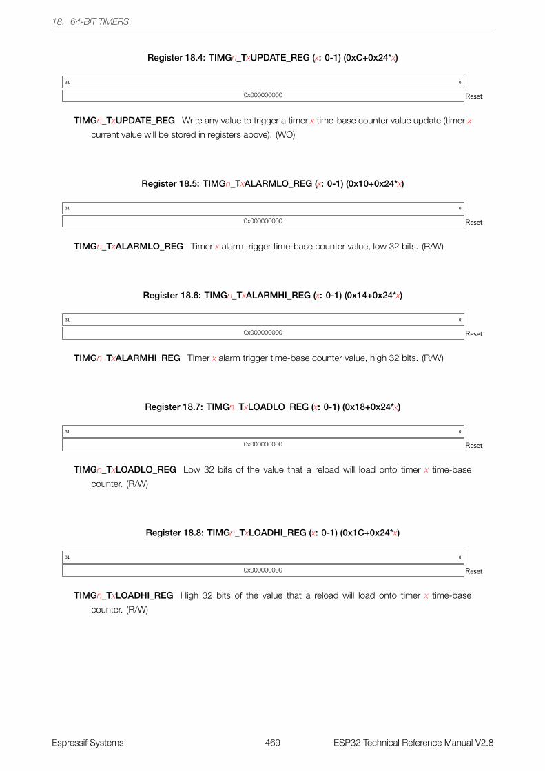
18. 64-BIT TIMERS
Register 18.4: TIMGn_TxUPDATE_REG (x: 0-1) (0xC+0x24*x)
0x000000000
31 0
Reset
TIMGn_TxUPDATE_REG Write any value to trigger a timer x time-base counter value update (timer x
current value will be stored in registers above). (WO)
Register 18.5: TIMGn_TxALARMLO_REG (x: 0-1) (0x10+0x24*x)
0x000000000
31 0
Reset
TIMGn_TxALARMLO_REG Timer x alarm trigger time-base counter value, low 32 bits. (R/W)
Register 18.6: TIMGn_TxALARMHI_REG (x: 0-1) (0x14+0x24*x)
0x000000000
31 0
Reset
TIMGn_TxALARMHI_REG Timer x alarm trigger time-base counter value, high 32 bits. (R/W)
Register 18.7: TIMGn_TxLOADLO_REG (x: 0-1) (0x18+0x24*x)
0x000000000
31 0
Reset
TIMGn_TxLOADLO_REG Low 32 bits of the value that a reload will load onto timer x time-base
counter. (R/W)
Register 18.8: TIMGn_TxLOADHI_REG (x: 0-1) (0x1C+0x24*x)
0x000000000
31 0
Reset
TIMGn_TxLOADHI_REG High 32 bits of the value that a reload will load onto timer x time-base
counter. (R/W)
Espressif Systems 469 ESP32 Technical Reference Manual V2.8
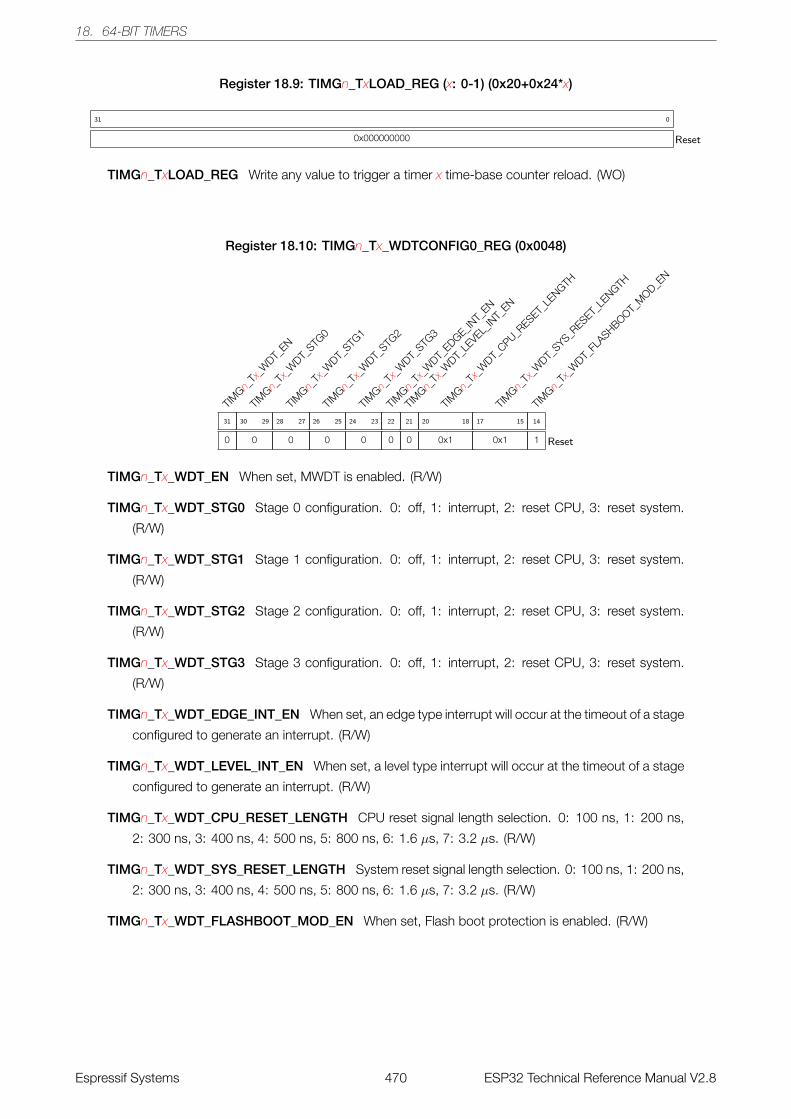
18. 64-BIT TIMERS
Register 18.9: TIMGn_TxLOAD_REG (x: 0-1) (0x20+0x24*x)
0x000000000
31 0
Reset
TIMGn_TxLOAD_REG Write any value to trigger a timer x time-base counter reload. (WO)
Register 18.10: TIMGn_Tx_WDTCONFIG0_REG (0x0048)
TIMGn
_Tx_
WDT_
EN
0
31
TIMGn
_Tx_
WDT_
STG0
0
30 29
TIMGn
_Tx_
WDT_
STG1
0
28 27
TIMGn
_Tx_
WDT_
STG2
0
26 25
TIMGn
_Tx_
WDT_
STG3
0
24 23
TIMGn
_Tx_
WDT_
EDGE_INT_
EN
0
22
TIMGn
_Tx_
WDT_
LEVEL_
INT_
EN
0
21
TIMGn
_Tx_
WDT_
CPU_RESET_
LENGTH
0x1
20 18
TIMGn
_Tx_
WDT_
SYS_RESET_
LENGTH
0x1
17 15
TIMGn
_Tx_
WDT_
FLASHBOOT_
MOD_E
N
1
14
Reset
TIMGn_Tx_WDT_EN When set, MWDT is enabled. (R/W)
TIMGn_Tx_WDT_STG0 Stage 0 configuration. 0: off, 1: interrupt, 2: reset CPU, 3: reset system.
(R/W)
TIMGn_Tx_WDT_STG1 Stage 1 configuration. 0: off, 1: interrupt, 2: reset CPU, 3: reset system.
(R/W)
TIMGn_Tx_WDT_STG2 Stage 2 configuration. 0: off, 1: interrupt, 2: reset CPU, 3: reset system.
(R/W)
TIMGn_Tx_WDT_STG3 Stage 3 configuration. 0: off, 1: interrupt, 2: reset CPU, 3: reset system.
(R/W)
TIMGn_Tx_WDT_EDGE_INT_EN When set, an edge type interrupt will occur at the timeout of a stage
configured to generate an interrupt. (R/W)
TIMGn_Tx_WDT_LEVEL_INT_EN When set, a level type interrupt will occur at the timeout of a stage
configured to generate an interrupt. (R/W)
TIMGn_Tx_WDT_CPU_RESET_LENGTH CPU reset signal length selection. 0: 100 ns, 1: 200 ns,
2: 300 ns, 3: 400 ns, 4: 500 ns, 5: 800 ns, 6: 1.6 µs, 7: 3.2 µs. (R/W)
TIMGn_Tx_WDT_SYS_RESET_LENGTH System reset signal length selection. 0: 100 ns, 1: 200 ns,
2: 300 ns, 3: 400 ns, 4: 500 ns, 5: 800 ns, 6: 1.6 µs, 7: 3.2 µs. (R/W)
TIMGn_Tx_WDT_FLASHBOOT_MOD_EN When set, Flash boot protection is enabled. (R/W)
Espressif Systems 470 ESP32 Technical Reference Manual V2.8
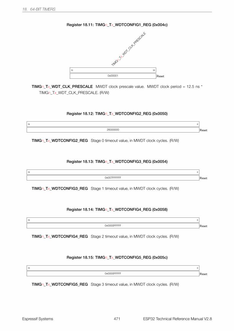
18. 64-BIT TIMERS
Register 18.11: TIMGn_Tx_WDTCONFIG1_REG (0x004c)
TIMGn
_Tx_
WDT_
CLK_P
RESCALE
0x00001
31 16
Reset
TIMGn_Tx_WDT_CLK_PRESCALE MWDT clock prescale value. MWDT clock period = 12.5 ns *
TIMGn_Tx_WDT_CLK_PRESCALE. (R/W)
Register 18.12: TIMGn_Tx_WDTCONFIG2_REG (0x0050)
26000000
31 0
Reset
TIMGn_Tx_WDTCONFIG2_REG Stage 0 timeout value, in MWDT clock cycles. (R/W)
Register 18.13: TIMGn_Tx_WDTCONFIG3_REG (0x0054)
0x007FFFFFF
31 0
Reset
TIMGn_Tx_WDTCONFIG3_REG Stage 1 timeout value, in MWDT clock cycles. (R/W)
Register 18.14: TIMGn_Tx_WDTCONFIG4_REG (0x0058)
0x0000FFFFF
31 0
Reset
TIMGn_Tx_WDTCONFIG4_REG Stage 2 timeout value, in MWDT clock cycles. (R/W)
Register 18.15: TIMGn_Tx_WDTCONFIG5_REG (0x005c)
0x0000FFFFF
31 0
Reset
TIMGn_Tx_WDTCONFIG5_REG Stage 3 timeout value, in MWDT clock cycles. (R/W)
Espressif Systems 471 ESP32 Technical Reference Manual V2.8
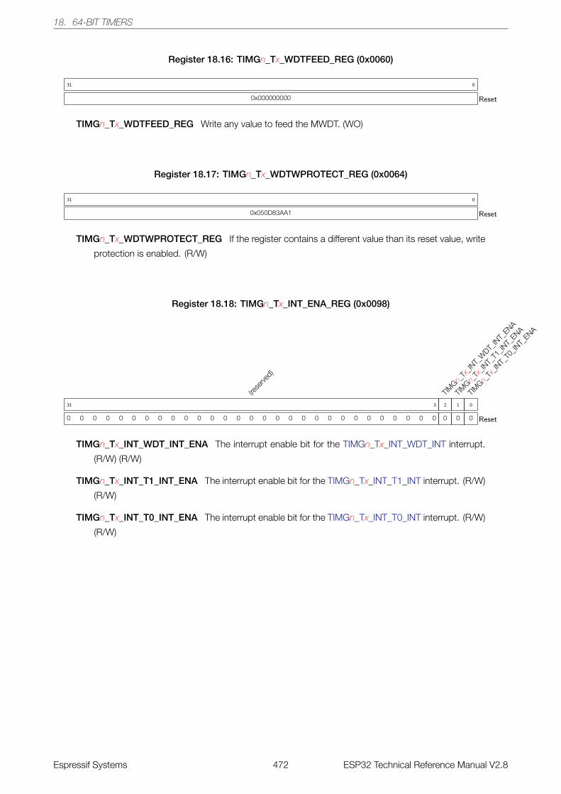
18. 64-BIT TIMERS
Register 18.16: TIMGn_Tx_WDTFEED_REG (0x0060)
0x000000000
31 0
Reset
TIMGn_Tx_WDTFEED_REG Write any value to feed the MWDT. (WO)
Register 18.17: TIMGn_Tx_WDTWPROTECT_REG (0x0064)
0x050D83AA1
31 0
Reset
TIMGn_Tx_WDTWPROTECT_REG If the register contains a different value than its reset value, write
protection is enabled. (R/W)
Register 18.18: TIMGn_Tx_INT_ENA_REG (0x0098)
(rese
rved)
0 0 0 0 0 0 0 0 0 0 0 0 0 0 0 0 0 0 0 0 0 0 0 0 0 0 0 0 0
31 3
TIMGn
_Tx_
INT_
WDT_
INT_
ENA
0
2
TIMGn
_Tx_
INT_
T1_IN
T_ENA
0
1
TIMGn
_Tx_
INT_
T0_IN
T_ENA
0
0
Reset
TIMGn_Tx_INT_WDT_INT_ENA The interrupt enable bit for the TIMGn_Tx_INT_WDT_INT interrupt.
(R/W) (R/W)
TIMGn_Tx_INT_T1_INT_ENA The interrupt enable bit for the TIMGn_Tx_INT_T1_INT interrupt. (R/W)
(R/W)
TIMGn_Tx_INT_T0_INT_ENA The interrupt enable bit for the TIMGn_Tx_INT_T0_INT interrupt. (R/W)
(R/W)
Espressif Systems 472 ESP32 Technical Reference Manual V2.8

18. 64-BIT TIMERS
Register 18.19: TIMGn_Tx_INT_RAW_REG (0x009c)
(rese
rved)
0 0 0 0 0 0 0 0 0 0 0 0 0 0 0 0 0 0 0 0 0 0 0 0 0 0 0 0 0
31 3
TIMGn
_Tx_
INT_
WDT_
INT_
RAW
0
2
TIMGn
_Tx_
INT_
T1_IN
T_RAW
0
1
TIMGn
_Tx_
INT_
T0_IN
T_RAW
0
0
Reset
TIMGn_Tx_INT_WDT_INT_RAW The raw interrupt status bit for the TIMGn_Tx_INT_WDT_INT inter-
rupt. (RO)
TIMGn_Tx_INT_T1_INT_RAW The raw interrupt status bit for the TIMGn_Tx_INT_T1_INT interrupt.
(RO)
TIMGn_Tx_INT_T0_INT_RAW The raw interrupt status bit for the TIMGn_Tx_INT_T0_INT interrupt.
(RO)
Register 18.20: TIMGn_Tx_INT_ST_REG (0x00a0)
(rese
rved)
0 0 0 0 0 0 0 0 0 0 0 0 0 0 0 0 0 0 0 0 0 0 0 0 0 0 0 0 0
31 3
TIMGn
_Tx_
INT_
WDT_
INT_
ST
0
2
TIMGn
_Tx_
INT_
T1_IN
T_ST
0
1
TIMGn
_Tx_
INT_
T0_IN
T_ST
0
0
Reset
TIMGn_Tx_INT_WDT_INT_ST The masked interrupt status bit for the TIMGn_Tx_INT_WDT_INT in-
terrupt. (RO)
TIMGn_Tx_INT_T1_INT_ST The masked interrupt status bit for the TIMGn_Tx_INT_T1_INT interrupt.
(RO)
TIMGn_Tx_INT_T0_INT_ST The masked interrupt status bit for the TIMGn_Tx_INT_T0_INT interrupt.
(RO)
Espressif Systems 473 ESP32 Technical Reference Manual V2.8
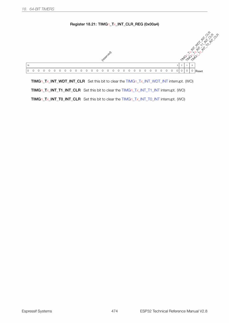
18. 64-BIT TIMERS
Register 18.21: TIMGn_Tx_INT_CLR_REG (0x00a4)
(rese
rved)
0 0 0 0 0 0 0 0 0 0 0 0 0 0 0 0 0 0 0 0 0 0 0 0 0 0 0 0 0
31 3
TIMGn
_Tx_
INT_
WDT_
INT_
CLR
0
2
TIMGn
_Tx_
INT_
T1_IN
T_CLR
0
1
TIMGn
_Tx_
INT_
T0_IN
T_CLR
0
0
Reset
TIMGn_Tx_INT_WDT_INT_CLR Set this bit to clear the TIMGn_Tx_INT_WDT_INT interrupt. (WO)
TIMGn_Tx_INT_T1_INT_CLR Set this bit to clear the TIMGn_Tx_INT_T1_INT interrupt. (WO)
TIMGn_Tx_INT_T0_INT_CLR Set this bit to clear the TIMGn_Tx_INT_T0_INT interrupt. (WO)
Espressif Systems 474 ESP32 Technical Reference Manual V2.8
19. WATCHDOG TIMERS
19. Watchdog Timers
19.1 Introduction
The ESP32 has three watchdog timers: one in each of the two timer modules (called Main System Watchdog
Timer, or MWDT) and one in the RTC module (which is called the RTC Watchdog Timer, or RWDT). These
watchdog timers are intended to recover from an unforeseen fault, causing the application program to abandon
its normal sequence. A watchdog timer has four stages. Each stage may take one out of three or four actions
upon the expiry of a programmed period of time for this stage, unless the watchdog is fed or disabled. The
actions are: interrupt, CPU reset, core reset and system reset. Only the RWDT can trigger the system reset, and
is able to reset the entire chip and the main system including the RTC itself. A timeout value can be set for each
stage individually.
During flash boot, the RWDT and the first MWDT start automatically in order to detect and recover from booting
problems.
19.2 Features
• Four stages, each of which can be configured or disabled separately
• Programmable time period for each stage
• One out of three or four possible actions (interrupt, CPU reset, core reset and system reset) upon the expiry
of each stage
• 32-bit expiry counter
• Write protection, to prevent the RWDT and MWDT configuration from being inadvertently altered.
• Flash boot protection
If the boot process from an SPI flash does not complete within a predetermined period of time, the
watchdog will reboot the entire main system.
19.3 Functional Description
19.3.1 Clock
The RWDT is clocked from the RTC slow clock, which usually will be 32 KHz. The MWDT clock source is derived
from the APB clock via a pre-MWDT 16-bit configurable prescaler. For either watchdog, the clock source is fed
into the 32-bit expiry counter. When this counter reaches the timeout value of the current stage, the action
configured for the stage will execute, the expiry counter will be reset and the next stage will become active.
Espressif Systems 475 ESP32 Technical Reference Manual V2.8
19. WATCHDOG TIMERS
19.3.1.1 Operating Procedure
When a watchdog timer is enabled, it will proceed in loops from stage 0 to stage 3, then back to stage 0 and
start again. The expiry action and time period for each stage can be configured individually.
Every stage can be configured for one of the following actions when the expiry timer reaches the stage’s timeout
value:
• Trigger an interrupt
When the stage expires an interrupt is triggered.
• Reset a CPU core
When the stage expires the designated CPU core will be reset. MWDT0 CPU reset only resets the PRO
CPU. MWDT1 CPU reset only resets the APP CPU. The RWDT CPU reset can reset either of them, or both,
or none, depending on configuration.
• Reset the main system
When the stage expires, the main system, including the MWDTs, will be reset. In this article, the main
system includes the CPU and all peripherals. The RTC is an exception to this, and it will not be reset.
• Reset the main system and RTC
When the stage expires the main system and the RTC will both be reset. This action is only available in the
RWDT.
• Disabled
This stage will have no effects on the system.
When software feeds the watchdog timer, it returns to stage 0 and its expiry counter restarts from 0.
19.3.1.2 Write Protection
Both the MWDTs, as well as the RWDT, can be protected from accidental writing. To accomplish this, they have
a write-key register (TIMERS_WDT_WKEY for the MWDT, RTC_CNTL_WDT_WKEY for the RWDT.) On reset,
these registers are initialized to the value 0x50D83AA1. When the value in this register is changed from
0x50D83AA1, write protection is enabled. Writes to any WDT register, including the feeding register (but
excluding the write-key register itself), are ignored. The recommended procedure for accessing a WDT is:
1. Disable the write protection
2. Make the required modification or feed the watchdog
3. Re-enable the write protection
19.3.1.3 Flash Boot Protection
During flash booting, the MWDT in timer group 0 (TIMG0), as well as the RWDT, are automatically enabled. Stage
0 for the enabled MWDT is automatically configured to reset the system upon expiry; stage 0 for the RWDT resets
the RTC when it expires. After booting, the register TIMERS_WDT_FLASHBOOT_MOD_EN should be cleared to
stop the flash boot protection procedure for the MWDT, and RTC_CNTL_WDT_FLASHBOOT_MOD_EN should
be cleared to do the same for the RWDT. After this, the MWDT and RWDT can be configured by software.
Espressif Systems 476 ESP32 Technical Reference Manual V2.8
19. WATCHDOG TIMERS
19.3.1.4 Registers
The MWDT registers are part of the timer submodule and are described in the Timer Registers section. The
RWDT registers are part of the RTC submodule and are described in the RTC Registers section.
Espressif Systems 477 ESP32 Technical Reference Manual V2.8
20. EFUSE CONTROLLER
20. eFuse Controller
20.1 Introduction
The ESP32 has a number of eFuses which store system parameters. Fundamentally, an eFuse is a single bit of
non-volatile memory with the restriction that once an eFuse bit is programmed to 1, it can never be reverted to 0.
Software can instruct the eFuse Controller to program each bit for each system parameter as needed.
Some of these system parameters can be read by software using the eFuse Controller. Some of the system
parameters are also directly used by hardware modules.
20.2 Features
• Configuration of 27 system parameters
• Optional write-protection
• Optional software-read-protection
20.3 Functional Description
20.3.1 Structure
Twenty-seven system parameters with different bit width are stored in the eFuses. The name of each system
parameter and the corresponding bit width are shown in Table 77. Among those parameters, efuse_wr_disable,
efuse_rd_disable, BLK3_part_reserve and coding_scheme are directly used by the eFuse Controller.
Table 77: System Parameter
Program Software-Read
-Protection by -Protection byName Bit width
efuse_wr_disable efuse_rd_disable
Description
efuse_wr_disable 16 1 - controls the eFuse Controller
efuse_rd_disable 4 0 - controls the eFuse Controller
flash_crypt_cnt 8 2 -governs the flash encryption/
decryption
WIFI_MAC_Address 56 3 - Wi-Fi MAC address and CRC
SPI_pad_config_hd 5 3 -configures the SPI I/O to a cer-
tain pad
chip_version 4 3 - chip version
XPD_SDIO_REG 1 5 - powers up the flash regulator
SDIO_TIEH 1 5 -
configures the flash regulator
voltage: set to 1 for 3.3 V
and set to 0 for 1.8 V
sdio_force 1 5 -
determines whether
XPD_SDIO_REG
and SDIO_TIEH can
control the flash regulator
Espressif Systems 478 ESP32 Technical Reference Manual V2.8

20. EFUSE CONTROLLER
Program Software-Read
-Protection by -Protection byName Bit width
efuse_wr_disable efuse_rd_disable
Description
BLK3_part_reseve 2 10 3 controls the eFuse controller
SPI_pad_config_clk 5 6 -configures the SPI I/O to a cer-
tain pad
SPI_pad_config_q 5 6 -configures the SPI I/O to a cer-
tain pad
SPI_pad_config_d 5 6 -configures the SPI I/O to a cer-
tain pad
SPI_pad_config_cs0 5 6 -configures the SPI I/O to a cer-
tain pad
flash_crypt_config 4 10 3governs flash encryption/
decryption
coding_scheme* 2 10 3 controls the eFuse Controller
console_debug_disable 1 15 -
Disables the ROM BASIC
debug console fallback
mode when set to 1
abstract_done_0 1 12 -determines the status of
Secure Boot
abstract_done_1 1 13 -determines the status of
Secure Boot
JTAG_disable 1 14 -
disables access to the
JTAG controllers so as to
effectively disable external
use of JTAG
download_dis_encrypt 1 15 -governs flash encryption/
decryption
download_dis_decrypt 1 15 -governs flash encryption/
decryption
download_dis_cache 1 15 -disables cache when boot
mode is the Download Mode
key_status 1 10 3determines whether BLOCK3
is deployed for user purposes
BLOCK1* 256/192/128 7 0governs flash encryption/
decryption
BLOCK2* 256/192/128 8 1 key for Secure Boot
BLOCK3* 256/192/128 9 2 key for user purposes
20.3.1.1 System Parameter efuse_wr_disable
The system parameter efuse_wr_disable determines whether all of the system parameters are write-protected.
Since efuse_wr_disable is a system parameter as well, it also determines whether it itself is
write-protected.
If a system parameter is not write-protected, its unprogrammed bits can be programmed from 0 to 1. The bits
Espressif Systems 479 ESP32 Technical Reference Manual V2.8
20. EFUSE CONTROLLER
previously programmed to 1 will remain 1. When a system parameter is write-protected, none of its bits can be
programmed: The unprogrammed bits will always remain 0 and the programmed bits will always remain 1.
The write-protection status of each system parameter corresponds to a bit in efuse_wr_disable. When the
corresponding bit is set to 0, the system parameter is not write-protected. When the corresponding bit is set to
1, the system parameter is write-protected. If a system parameter is already write-protected, it will remain
write-protected. The column entitled ”Program-Protection by efuse_wr_disable” in Table 77 lists the
corresponding bits that determine the write-protection status of each system parameter.
20.3.1.2 System Parameter efuse_rd_disable
Of the 26 system parameters, 20 are not constrained by software-read-protection. These are marked by ”-” in
the column entitled ”Software-Read-Protection by efuse_rd_disable” in Table 77. Those system parameters,
some of which are used by software and hardware modules at the same time, can be read by software via the
eFuse Controller at any time.
When not software-read-protected, the other six system parameters can both be read by software and used by
hardware modules. When they are software-read-protected, they can only be used by the hardware
modules.
The column ”Software-Read-Protection by efuse_rd_disable” in Table 77 lists the corresponding bits in
efuse_rd_disable that determine the software read-protection status of the six system parameters. If a bit in the
system parameter efuse_rd_disable is 0, the system parameter controlled by the bit is not
software-read-protected. If a bit in the system parameter efuse_rd_disable is 1, the system parameter controlled
by the bit is software-read-protected. If a system parameter is software-read-protected, it will remain in this
state.
20.3.1.3 System Parameter coding_scheme
As Table 77 shows, only three system parameters, BLOCK1, BLOCK2, and BLOCK3, have variable bit width.
Their bit width is controlled by another system parameter, coding_scheme. Despite their variable bit width,
BLOCK1, BLOCK2, and BLOCK3 are assigned a fixed number of bits in eFuse. There is an encoding mapping
between these three system parameters and their corresponding stored values in eFuse. For details please see
Table 78.
Table 78: BLOCK1/2/3 Encoding
coding_scheme[1:0] Width of BLOCK1/2/3 Coding scheme Number of bits in eFuse
00/11 256 None 256
01 192 3/4 256
10 128 Repeat 256
The three coding schemes are explained as follows:
• BLOCKN represents any of the following three system parameters: BLOCK1, BLOCK2 or BLOCK3.
• BLOCKN [255 : 0], BLOCKN [191 : 0], and BLOCKN [127 : 0] represent each bit of the three system
parameters in the three encoding schemes.
Espressif Systems 480 ESP32 Technical Reference Manual V2.8
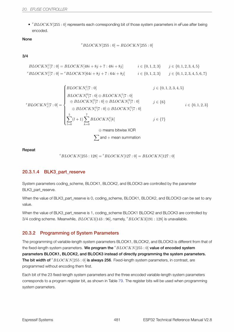
20. EFUSE CONTROLLER
• eBLOCKN [255 : 0] represents each corresponding bit of those system parameters in eFuse after being
encoded.
NoneeBLOCKN [255 : 0] = BLOCKN [255 : 0]
3/4
BLOCKN ji [7 : 0] = BLOCKN [48i+ 8j + 7 : 48i+ 8j] i ∈ {0, 1, 2, 3} j ∈ {0, 1, 2, 3, 4, 5}
eBLOCKN ji [7 : 0] = eBLOCKN [64i+ 8j + 7 : 64i+ 8j] i ∈ {0, 1, 2, 3} j ∈ {0, 1, 2, 3, 4, 5, 6, 7}
eBLOCKN ji [7 : 0] =
BLOCKN ji [7 : 0] j ∈ {0, 1, 2, 3, 4, 5}
BLOCKN0i [7 : 0]⊕BLOCKN1
i [7 : 0]
⊕BLOCKN2i [7 : 0]⊕BLOCKN3
i [7 : 0]
⊕BLOCKN4i [7 : 0]⊕BLOCKN5
i [7 : 0]
j ∈ {6}
5∑l=0
(l + 1)
7∑k=0
BLOCKN li [k] j ∈ {7}
i ∈ {0, 1, 2, 3}
⊕ means bitwise XOR∑and + mean summation
RepeateBLOCKN [255 : 128] =
eBLOCKN [127 : 0] = BLOCKN [127 : 0]
20.3.1.4 BLK3_part_reserve
System parameters coding_scheme, BLOCK1, BLOCK2, and BLOCK3 are controlled by the parameter
BLK3_part_reserve.
When the value of BLK3_part_reserve is 0, coding_scheme, BLOCK1, BLOCK2, and BLOCK3 can be set to any
value.
When the value of BLK3_part_reserve is 1, coding_scheme�BLOCK1�BLOCK2 and BLOCK3 are controlled by
3/4 coding scheme. Meanwhile, BLOCK3[143 : 96], namely, eBLOCK3[191 : 128] is unavailable.
20.3.2 Programming of System Parameters
The programming of variable-length system parameters BLOCK1, BLOCK2, and BLOCK3 is different from that of
the fixed-length system parameters. We program the eBLOCKN [255 : 0] value of encoded system
parameters BLOCK1, BLOCK2, and BLOCK3 instead of directly programming the system parameters.
The bit width of eBLOCKN [255 : 0] is always 256. Fixed-length system parameters, in contrast, are
programmed without encoding them first.
Each bit of the 23 fixed-length system parameters and the three encoded variable-length system parameters
corresponds to a program register bit, as shown in Table 79. The register bits will be used when programming
system parameters.
Espressif Systems 481 ESP32 Technical Reference Manual V2.8
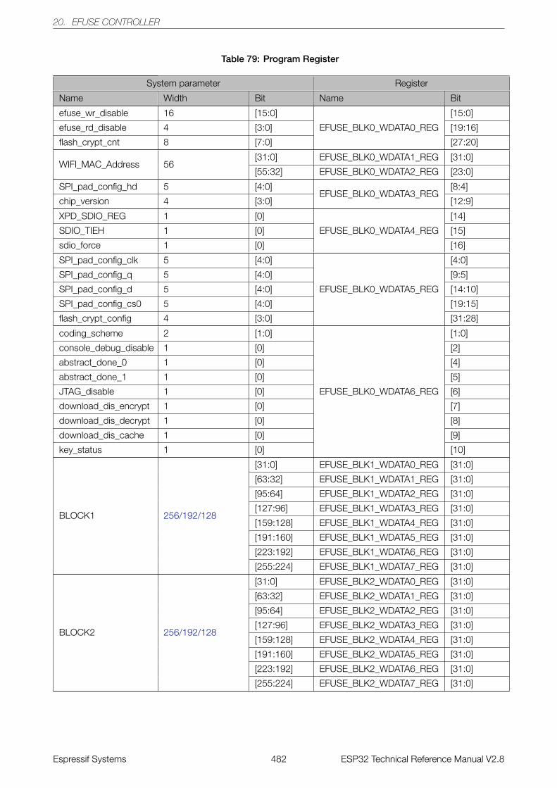
20. EFUSE CONTROLLER
Table 79: Program Register
System parameter Register
Name Width Bit Name Bit
efuse_wr_disable 16 [15:0]
EFUSE_BLK0_WDATA0_REG
[15:0]
efuse_rd_disable 4 [3:0] [19:16]
flash_crypt_cnt 8 [7:0] [27:20]
WIFI_MAC_Address 56[31:0] EFUSE_BLK0_WDATA1_REG [31:0]
[55:32] EFUSE_BLK0_WDATA2_REG [23:0]
SPI_pad_config_hd 5 [4:0]EFUSE_BLK0_WDATA3_REG
[8:4]
chip_version 4 [3:0] [12:9]
XPD_SDIO_REG 1 [0]
EFUSE_BLK0_WDATA4_REG
[14]
SDIO_TIEH 1 [0] [15]
sdio_force 1 [0] [16]
SPI_pad_config_clk 5 [4:0]
EFUSE_BLK0_WDATA5_REG
[4:0]
SPI_pad_config_q 5 [4:0] [9:5]
SPI_pad_config_d 5 [4:0] [14:10]
SPI_pad_config_cs0 5 [4:0] [19:15]
flash_crypt_config 4 [3:0] [31:28]
coding_scheme 2 [1:0]
EFUSE_BLK0_WDATA6_REG
[1:0]
console_debug_disable 1 [0] [2]
abstract_done_0 1 [0] [4]
abstract_done_1 1 [0] [5]
JTAG_disable 1 [0] [6]
download_dis_encrypt 1 [0] [7]
download_dis_decrypt 1 [0] [8]
download_dis_cache 1 [0] [9]
key_status 1 [0] [10]
BLOCK1 256/192/128
[31:0] EFUSE_BLK1_WDATA0_REG [31:0]
[63:32] EFUSE_BLK1_WDATA1_REG [31:0]
[95:64] EFUSE_BLK1_WDATA2_REG [31:0]
[127:96] EFUSE_BLK1_WDATA3_REG [31:0]
[159:128] EFUSE_BLK1_WDATA4_REG [31:0]
[191:160] EFUSE_BLK1_WDATA5_REG [31:0]
[223:192] EFUSE_BLK1_WDATA6_REG [31:0]
[255:224] EFUSE_BLK1_WDATA7_REG [31:0]
BLOCK2 256/192/128
[31:0] EFUSE_BLK2_WDATA0_REG [31:0]
[63:32] EFUSE_BLK2_WDATA1_REG [31:0]
[95:64] EFUSE_BLK2_WDATA2_REG [31:0]
[127:96] EFUSE_BLK2_WDATA3_REG [31:0]
[159:128] EFUSE_BLK2_WDATA4_REG [31:0]
[191:160] EFUSE_BLK2_WDATA5_REG [31:0]
[223:192] EFUSE_BLK2_WDATA6_REG [31:0]
[255:224] EFUSE_BLK2_WDATA7_REG [31:0]
Espressif Systems 482 ESP32 Technical Reference Manual V2.8
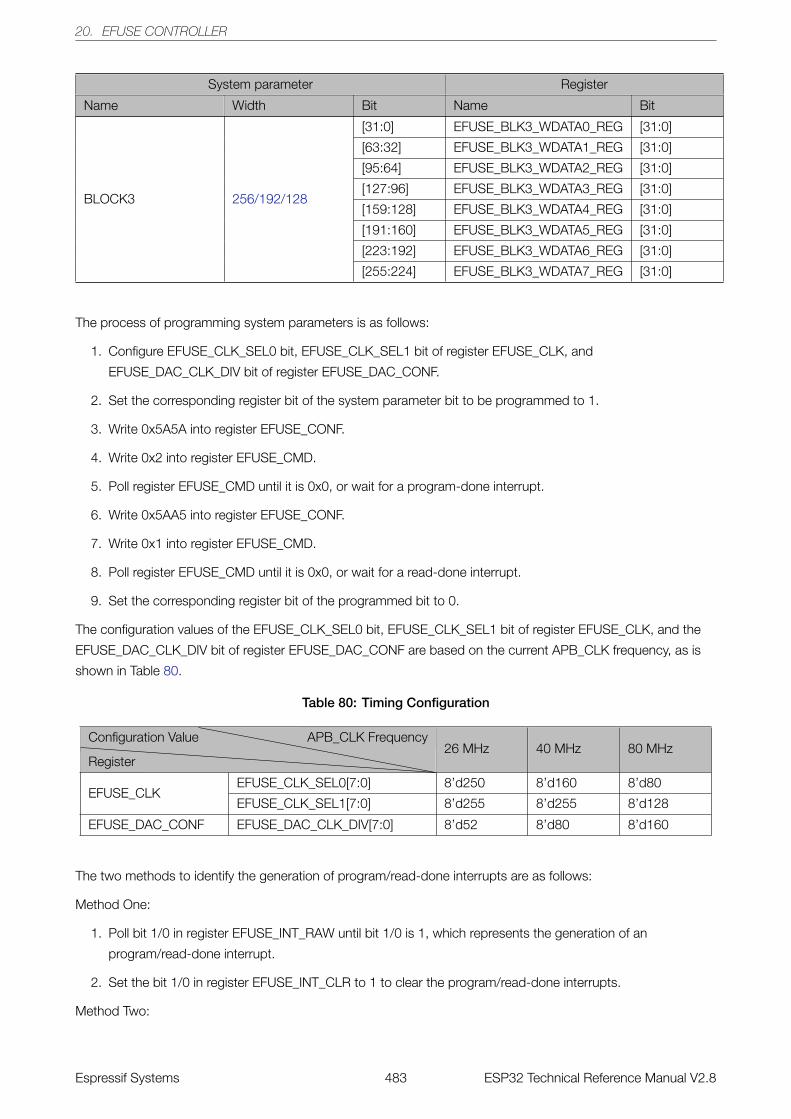
20. EFUSE CONTROLLER
System parameter Register
Name Width Bit Name Bit
BLOCK3 256/192/128
[31:0] EFUSE_BLK3_WDATA0_REG [31:0]
[63:32] EFUSE_BLK3_WDATA1_REG [31:0]
[95:64] EFUSE_BLK3_WDATA2_REG [31:0]
[127:96] EFUSE_BLK3_WDATA3_REG [31:0]
[159:128] EFUSE_BLK3_WDATA4_REG [31:0]
[191:160] EFUSE_BLK3_WDATA5_REG [31:0]
[223:192] EFUSE_BLK3_WDATA6_REG [31:0]
[255:224] EFUSE_BLK3_WDATA7_REG [31:0]
The process of programming system parameters is as follows:
1. Configure EFUSE_CLK_SEL0 bit, EFUSE_CLK_SEL1 bit of register EFUSE_CLK, and
EFUSE_DAC_CLK_DIV bit of register EFUSE_DAC_CONF.
2. Set the corresponding register bit of the system parameter bit to be programmed to 1.
3. Write 0x5A5A into register EFUSE_CONF.
4. Write 0x2 into register EFUSE_CMD.
5. Poll register EFUSE_CMD until it is 0x0, or wait for a program-done interrupt.
6. Write 0x5AA5 into register EFUSE_CONF.
7. Write 0x1 into register EFUSE_CMD.
8. Poll register EFUSE_CMD until it is 0x0, or wait for a read-done interrupt.
9. Set the corresponding register bit of the programmed bit to 0.
The configuration values of the EFUSE_CLK_SEL0 bit, EFUSE_CLK_SEL1 bit of register EFUSE_CLK, and the
EFUSE_DAC_CLK_DIV bit of register EFUSE_DAC_CONF are based on the current APB_CLK frequency, as is
shown in Table 80.
Table 80: Timing Configuration
Register
Configuration Value APB_CLK Frequency26 MHz 40 MHz 80 MHz
EFUSE_CLKEFUSE_CLK_SEL0[7:0] 8’d250 8’d160 8’d80
EFUSE_CLK_SEL1[7:0] 8’d255 8’d255 8’d128
EFUSE_DAC_CONF EFUSE_DAC_CLK_DIV[7:0] 8’d52 8’d80 8’d160
The two methods to identify the generation of program/read-done interrupts are as follows:
Method One:
1. Poll bit 1/0 in register EFUSE_INT_RAW until bit 1/0 is 1, which represents the generation of an
program/read-done interrupt.
2. Set the bit 1/0 in register EFUSE_INT_CLR to 1 to clear the program/read-done interrupts.
Method Two:
Espressif Systems 483 ESP32 Technical Reference Manual V2.8
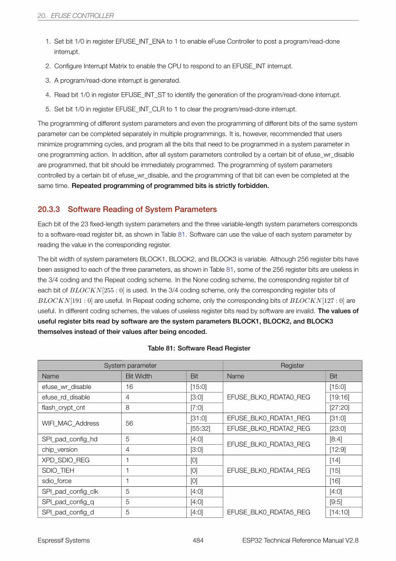
20. EFUSE CONTROLLER
1. Set bit 1/0 in register EFUSE_INT_ENA to 1 to enable eFuse Controller to post a program/read-done
interrupt.
2. Configure Interrupt Matrix to enable the CPU to respond to an EFUSE_INT interrupt.
3. A program/read-done interrupt is generated.
4. Read bit 1/0 in register EFUSE_INT_ST to identify the generation of the program/read-done interrupt.
5. Set bit 1/0 in register EFUSE_INT_CLR to 1 to clear the program/read-done interrupt.
The programming of different system parameters and even the programming of different bits of the same system
parameter can be completed separately in multiple programmings. It is, however, recommended that users
minimize programming cycles, and program all the bits that need to be programmed in a system parameter in
one programming action. In addition, after all system parameters controlled by a certain bit of efuse_wr_disable
are programmed, that bit should be immediately programmed. The programming of system parameters
controlled by a certain bit of efuse_wr_disable, and the programming of that bit can even be completed at the
same time. Repeated programming of programmed bits is strictly forbidden.
20.3.3 Software Reading of System Parameters
Each bit of the 23 fixed-length system parameters and the three variable-length system parameters corresponds
to a software-read register bit, as shown in Table 81. Software can use the value of each system parameter by
reading the value in the corresponding register.
The bit width of system parameters BLOCK1, BLOCK2, and BLOCK3 is variable. Although 256 register bits have
been assigned to each of the three parameters, as shown in Table 81, some of the 256 register bits are useless in
the 3/4 coding and the Repeat coding scheme. In the None coding scheme, the corresponding register bit of
each bit of BLOCKN [255 : 0] is used. In the 3/4 coding scheme, only the corresponding register bits of
BLOCKN [191 : 0] are useful. In Repeat coding scheme, only the corresponding bits of BLOCKN [127 : 0] are
useful. In different coding schemes, the values of useless register bits read by software are invalid. The values of
useful register bits read by software are the system parameters BLOCK1, BLOCK2, and BLOCK3
themselves instead of their values after being encoded.
Table 81: Software Read Register
System parameter Register
Name Bit Width Bit Name Bit
efuse_wr_disable 16 [15:0]
EFUSE_BLK0_RDATA0_REG
[15:0]
efuse_rd_disable 4 [3:0] [19:16]
flash_crypt_cnt 8 [7:0] [27:20]
WIFI_MAC_Address 56[31:0] EFUSE_BLK0_RDATA1_REG [31:0]
[55:32] EFUSE_BLK0_RDATA2_REG [23:0]
SPI_pad_config_hd 5 [4:0]EFUSE_BLK0_RDATA3_REG
[8:4]
chip_version 4 [3:0] [12:9]
XPD_SDIO_REG 1 [0]
EFUSE_BLK0_RDATA4_REG
[14]
SDIO_TIEH 1 [0] [15]
sdio_force 1 [0] [16]
SPI_pad_config_clk 5 [4:0]
EFUSE_BLK0_RDATA5_REG
[4:0]
SPI_pad_config_q 5 [4:0] [9:5]
SPI_pad_config_d 5 [4:0] [14:10]
Espressif Systems 484 ESP32 Technical Reference Manual V2.8
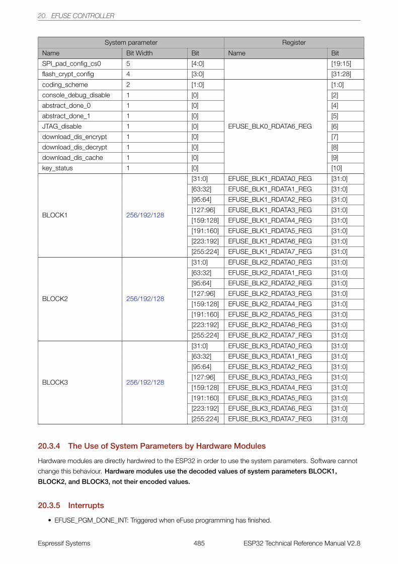
20. EFUSE CONTROLLER
System parameter Register
Name Bit Width Bit Name Bit
SPI_pad_config_cs0 5 [4:0] [19:15]
flash_crypt_config 4 [3:0] [31:28]
coding_scheme 2 [1:0]
EFUSE_BLK0_RDATA6_REG
[1:0]
console_debug_disable 1 [0] [2]
abstract_done_0 1 [0] [4]
abstract_done_1 1 [0] [5]
JTAG_disable 1 [0] [6]
download_dis_encrypt 1 [0] [7]
download_dis_decrypt 1 [0] [8]
download_dis_cache 1 [0] [9]
key_status 1 [0] [10]
BLOCK1 256/192/128
[31:0] EFUSE_BLK1_RDATA0_REG [31:0]
[63:32] EFUSE_BLK1_RDATA1_REG [31:0]
[95:64] EFUSE_BLK1_RDATA2_REG [31:0]
[127:96] EFUSE_BLK1_RDATA3_REG [31:0]
[159:128] EFUSE_BLK1_RDATA4_REG [31:0]
[191:160] EFUSE_BLK1_RDATA5_REG [31:0]
[223:192] EFUSE_BLK1_RDATA6_REG [31:0]
[255:224] EFUSE_BLK1_RDATA7_REG [31:0]
BLOCK2 256/192/128
[31:0] EFUSE_BLK2_RDATA0_REG [31:0]
[63:32] EFUSE_BLK2_RDATA1_REG [31:0]
[95:64] EFUSE_BLK2_RDATA2_REG [31:0]
[127:96] EFUSE_BLK2_RDATA3_REG [31:0]
[159:128] EFUSE_BLK2_RDATA4_REG [31:0]
[191:160] EFUSE_BLK2_RDATA5_REG [31:0]
[223:192] EFUSE_BLK2_RDATA6_REG [31:0]
[255:224] EFUSE_BLK2_RDATA7_REG [31:0]
BLOCK3 256/192/128
[31:0] EFUSE_BLK3_RDATA0_REG [31:0]
[63:32] EFUSE_BLK3_RDATA1_REG [31:0]
[95:64] EFUSE_BLK3_RDATA2_REG [31:0]
[127:96] EFUSE_BLK3_RDATA3_REG [31:0]
[159:128] EFUSE_BLK3_RDATA4_REG [31:0]
[191:160] EFUSE_BLK3_RDATA5_REG [31:0]
[223:192] EFUSE_BLK3_RDATA6_REG [31:0]
[255:224] EFUSE_BLK3_RDATA7_REG [31:0]
20.3.4 The Use of System Parameters by Hardware Modules
Hardware modules are directly hardwired to the ESP32 in order to use the system parameters. Software cannot
change this behaviour. Hardware modules use the decoded values of system parameters BLOCK1,
BLOCK2, and BLOCK3, not their encoded values.
20.3.5 Interrupts
• EFUSE_PGM_DONE_INT: Triggered when eFuse programming has finished.
Espressif Systems 485 ESP32 Technical Reference Manual V2.8
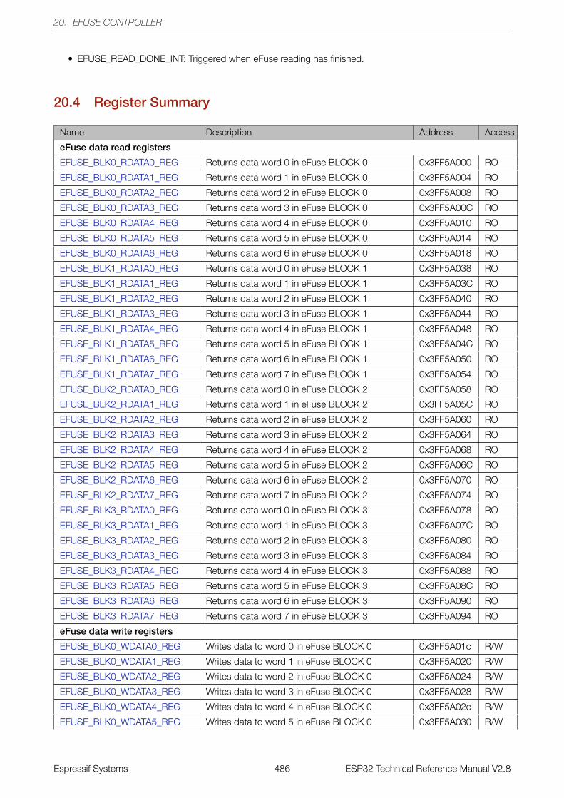
20. EFUSE CONTROLLER
• EFUSE_READ_DONE_INT: Triggered when eFuse reading has finished.
20.4 Register Summary
Name Description Address Access
eFuse data read registers
EFUSE_BLK0_RDATA0_REG Returns data word 0 in eFuse BLOCK 0 0x3FF5A000 RO
EFUSE_BLK0_RDATA1_REG Returns data word 1 in eFuse BLOCK 0 0x3FF5A004 RO
EFUSE_BLK0_RDATA2_REG Returns data word 2 in eFuse BLOCK 0 0x3FF5A008 RO
EFUSE_BLK0_RDATA3_REG Returns data word 3 in eFuse BLOCK 0 0x3FF5A00C RO
EFUSE_BLK0_RDATA4_REG Returns data word 4 in eFuse BLOCK 0 0x3FF5A010 RO
EFUSE_BLK0_RDATA5_REG Returns data word 5 in eFuse BLOCK 0 0x3FF5A014 RO
EFUSE_BLK0_RDATA6_REG Returns data word 6 in eFuse BLOCK 0 0x3FF5A018 RO
EFUSE_BLK1_RDATA0_REG Returns data word 0 in eFuse BLOCK 1 0x3FF5A038 RO
EFUSE_BLK1_RDATA1_REG Returns data word 1 in eFuse BLOCK 1 0x3FF5A03C RO
EFUSE_BLK1_RDATA2_REG Returns data word 2 in eFuse BLOCK 1 0x3FF5A040 RO
EFUSE_BLK1_RDATA3_REG Returns data word 3 in eFuse BLOCK 1 0x3FF5A044 RO
EFUSE_BLK1_RDATA4_REG Returns data word 4 in eFuse BLOCK 1 0x3FF5A048 RO
EFUSE_BLK1_RDATA5_REG Returns data word 5 in eFuse BLOCK 1 0x3FF5A04C RO
EFUSE_BLK1_RDATA6_REG Returns data word 6 in eFuse BLOCK 1 0x3FF5A050 RO
EFUSE_BLK1_RDATA7_REG Returns data word 7 in eFuse BLOCK 1 0x3FF5A054 RO
EFUSE_BLK2_RDATA0_REG Returns data word 0 in eFuse BLOCK 2 0x3FF5A058 RO
EFUSE_BLK2_RDATA1_REG Returns data word 1 in eFuse BLOCK 2 0x3FF5A05C RO
EFUSE_BLK2_RDATA2_REG Returns data word 2 in eFuse BLOCK 2 0x3FF5A060 RO
EFUSE_BLK2_RDATA3_REG Returns data word 3 in eFuse BLOCK 2 0x3FF5A064 RO
EFUSE_BLK2_RDATA4_REG Returns data word 4 in eFuse BLOCK 2 0x3FF5A068 RO
EFUSE_BLK2_RDATA5_REG Returns data word 5 in eFuse BLOCK 2 0x3FF5A06C RO
EFUSE_BLK2_RDATA6_REG Returns data word 6 in eFuse BLOCK 2 0x3FF5A070 RO
EFUSE_BLK2_RDATA7_REG Returns data word 7 in eFuse BLOCK 2 0x3FF5A074 RO
EFUSE_BLK3_RDATA0_REG Returns data word 0 in eFuse BLOCK 3 0x3FF5A078 RO
EFUSE_BLK3_RDATA1_REG Returns data word 1 in eFuse BLOCK 3 0x3FF5A07C RO
EFUSE_BLK3_RDATA2_REG Returns data word 2 in eFuse BLOCK 3 0x3FF5A080 RO
EFUSE_BLK3_RDATA3_REG Returns data word 3 in eFuse BLOCK 3 0x3FF5A084 RO
EFUSE_BLK3_RDATA4_REG Returns data word 4 in eFuse BLOCK 3 0x3FF5A088 RO
EFUSE_BLK3_RDATA5_REG Returns data word 5 in eFuse BLOCK 3 0x3FF5A08C RO
EFUSE_BLK3_RDATA6_REG Returns data word 6 in eFuse BLOCK 3 0x3FF5A090 RO
EFUSE_BLK3_RDATA7_REG Returns data word 7 in eFuse BLOCK 3 0x3FF5A094 RO
eFuse data write registers
EFUSE_BLK0_WDATA0_REG Writes data to word 0 in eFuse BLOCK 0 0x3FF5A01c R/W
EFUSE_BLK0_WDATA1_REG Writes data to word 1 in eFuse BLOCK 0 0x3FF5A020 R/W
EFUSE_BLK0_WDATA2_REG Writes data to word 2 in eFuse BLOCK 0 0x3FF5A024 R/W
EFUSE_BLK0_WDATA3_REG Writes data to word 3 in eFuse BLOCK 0 0x3FF5A028 R/W
EFUSE_BLK0_WDATA4_REG Writes data to word 4 in eFuse BLOCK 0 0x3FF5A02c R/W
EFUSE_BLK0_WDATA5_REG Writes data to word 5 in eFuse BLOCK 0 0x3FF5A030 R/W
Espressif Systems 486 ESP32 Technical Reference Manual V2.8
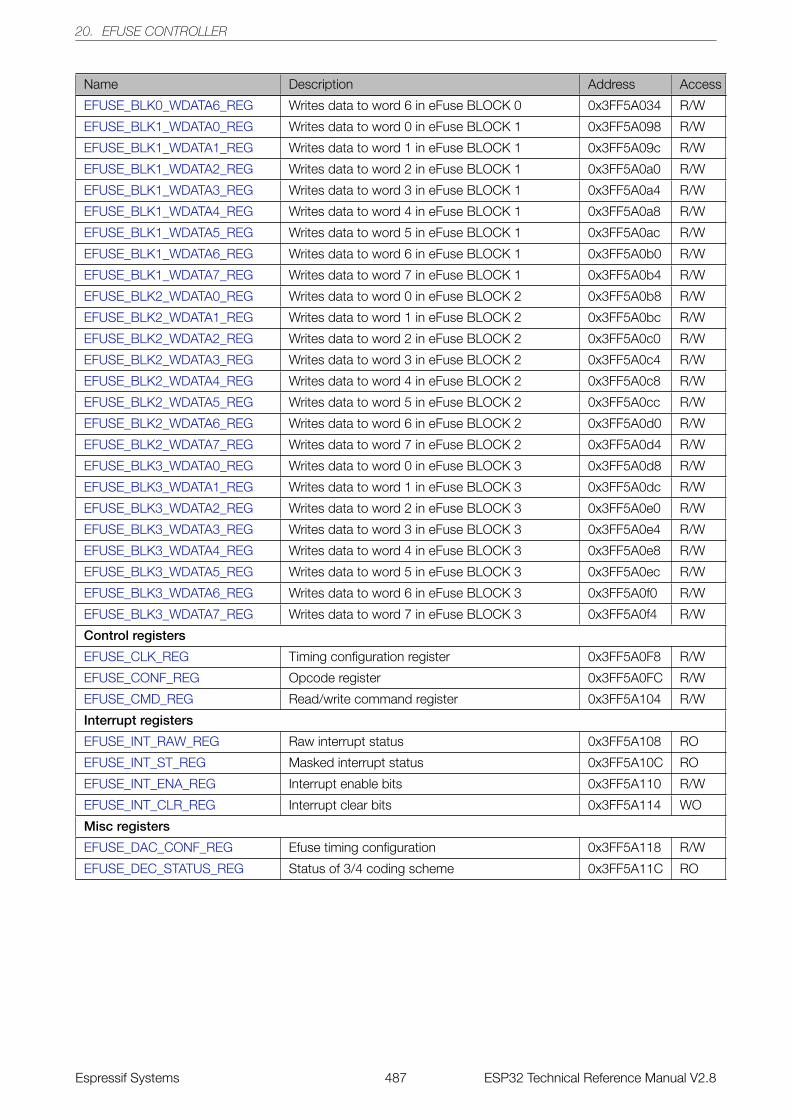
20. EFUSE CONTROLLER
Name Description Address Access
EFUSE_BLK0_WDATA6_REG Writes data to word 6 in eFuse BLOCK 0 0x3FF5A034 R/W
EFUSE_BLK1_WDATA0_REG Writes data to word 0 in eFuse BLOCK 1 0x3FF5A098 R/W
EFUSE_BLK1_WDATA1_REG Writes data to word 1 in eFuse BLOCK 1 0x3FF5A09c R/W
EFUSE_BLK1_WDATA2_REG Writes data to word 2 in eFuse BLOCK 1 0x3FF5A0a0 R/W
EFUSE_BLK1_WDATA3_REG Writes data to word 3 in eFuse BLOCK 1 0x3FF5A0a4 R/W
EFUSE_BLK1_WDATA4_REG Writes data to word 4 in eFuse BLOCK 1 0x3FF5A0a8 R/W
EFUSE_BLK1_WDATA5_REG Writes data to word 5 in eFuse BLOCK 1 0x3FF5A0ac R/W
EFUSE_BLK1_WDATA6_REG Writes data to word 6 in eFuse BLOCK 1 0x3FF5A0b0 R/W
EFUSE_BLK1_WDATA7_REG Writes data to word 7 in eFuse BLOCK 1 0x3FF5A0b4 R/W
EFUSE_BLK2_WDATA0_REG Writes data to word 0 in eFuse BLOCK 2 0x3FF5A0b8 R/W
EFUSE_BLK2_WDATA1_REG Writes data to word 1 in eFuse BLOCK 2 0x3FF5A0bc R/W
EFUSE_BLK2_WDATA2_REG Writes data to word 2 in eFuse BLOCK 2 0x3FF5A0c0 R/W
EFUSE_BLK2_WDATA3_REG Writes data to word 3 in eFuse BLOCK 2 0x3FF5A0c4 R/W
EFUSE_BLK2_WDATA4_REG Writes data to word 4 in eFuse BLOCK 2 0x3FF5A0c8 R/W
EFUSE_BLK2_WDATA5_REG Writes data to word 5 in eFuse BLOCK 2 0x3FF5A0cc R/W
EFUSE_BLK2_WDATA6_REG Writes data to word 6 in eFuse BLOCK 2 0x3FF5A0d0 R/W
EFUSE_BLK2_WDATA7_REG Writes data to word 7 in eFuse BLOCK 2 0x3FF5A0d4 R/W
EFUSE_BLK3_WDATA0_REG Writes data to word 0 in eFuse BLOCK 3 0x3FF5A0d8 R/W
EFUSE_BLK3_WDATA1_REG Writes data to word 1 in eFuse BLOCK 3 0x3FF5A0dc R/W
EFUSE_BLK3_WDATA2_REG Writes data to word 2 in eFuse BLOCK 3 0x3FF5A0e0 R/W
EFUSE_BLK3_WDATA3_REG Writes data to word 3 in eFuse BLOCK 3 0x3FF5A0e4 R/W
EFUSE_BLK3_WDATA4_REG Writes data to word 4 in eFuse BLOCK 3 0x3FF5A0e8 R/W
EFUSE_BLK3_WDATA5_REG Writes data to word 5 in eFuse BLOCK 3 0x3FF5A0ec R/W
EFUSE_BLK3_WDATA6_REG Writes data to word 6 in eFuse BLOCK 3 0x3FF5A0f0 R/W
EFUSE_BLK3_WDATA7_REG Writes data to word 7 in eFuse BLOCK 3 0x3FF5A0f4 R/W
Control registers
EFUSE_CLK_REG Timing configuration register 0x3FF5A0F8 R/W
EFUSE_CONF_REG Opcode register 0x3FF5A0FC R/W
EFUSE_CMD_REG Read/write command register 0x3FF5A104 R/W
Interrupt registers
EFUSE_INT_RAW_REG Raw interrupt status 0x3FF5A108 RO
EFUSE_INT_ST_REG Masked interrupt status 0x3FF5A10C RO
EFUSE_INT_ENA_REG Interrupt enable bits 0x3FF5A110 R/W
EFUSE_INT_CLR_REG Interrupt clear bits 0x3FF5A114 WO
Misc registers
EFUSE_DAC_CONF_REG Efuse timing configuration 0x3FF5A118 R/W
EFUSE_DEC_STATUS_REG Status of 3/4 coding scheme 0x3FF5A11C RO
Espressif Systems 487 ESP32 Technical Reference Manual V2.8
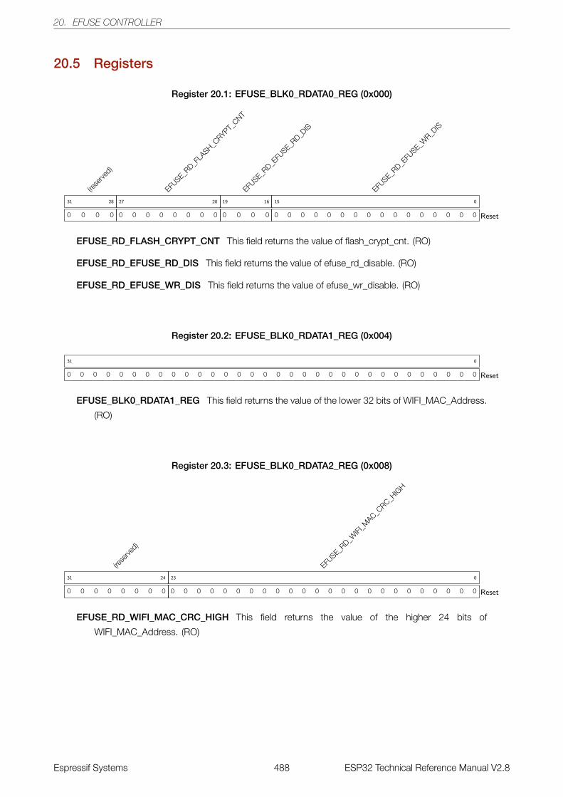
20. EFUSE CONTROLLER
20.5 Registers
Register 20.1: EFUSE_BLK0_RDATA0_REG (0x000)
(rese
rved)
0 0 0 0
31 28
EFUSE_R
D_FLA
SH_CRYPT_
CNT
0 0 0 0 0 0 0 0
27 20
EFUSE_R
D_EFU
SE_RD_D
IS
0 0 0 0
19 16
EFUSE_R
D_EFU
SE_WR_D
IS
0 0 0 0 0 0 0 0 0 0 0 0 0 0 0 0
15 0
Reset
EFUSE_RD_FLASH_CRYPT_CNT This field returns the value of flash_crypt_cnt. (RO)
EFUSE_RD_EFUSE_RD_DIS This field returns the value of efuse_rd_disable. (RO)
EFUSE_RD_EFUSE_WR_DIS This field returns the value of efuse_wr_disable. (RO)
Register 20.2: EFUSE_BLK0_RDATA1_REG (0x004)
0 0 0 0 0 0 0 0 0 0 0 0 0 0 0 0 0 0 0 0 0 0 0 0 0 0 0 0 0 0 0 0
31 0
Reset
EFUSE_BLK0_RDATA1_REG This field returns the value of the lower 32 bits of WIFI_MAC_Address.
(RO)
Register 20.3: EFUSE_BLK0_RDATA2_REG (0x008)
(rese
rved)
0 0 0 0 0 0 0 0
31 24
EFUSE_R
D_WIFI
_MAC_C
RC_HIG
H
0 0 0 0 0 0 0 0 0 0 0 0 0 0 0 0 0 0 0 0 0 0 0 0
23 0
Reset
EFUSE_RD_WIFI_MAC_CRC_HIGH This field returns the value of the higher 24 bits of
WIFI_MAC_Address. (RO)
Espressif Systems 488 ESP32 Technical Reference Manual V2.8
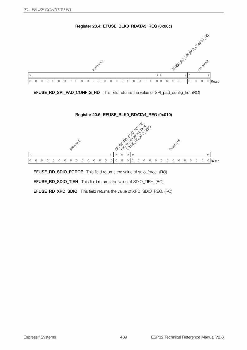
20. EFUSE CONTROLLER
Register 20.4: EFUSE_BLK0_RDATA3_REG (0x00c)
(rese
rved)
0 0 0 0 0 0 0 0 0 0 0 0 0 0 0 0 0 0 0 0 0 0 0
31 9
EFUSE_R
D_SPI_P
AD_CONFIG
_HD
0 0 0 0 0
8 4
(rese
rved)
0 0 0 0
7 4
Reset
EFUSE_RD_SPI_PAD_CONFIG_HD This field returns the value of SPI_pad_config_hd. (RO)
Register 20.5: EFUSE_BLK0_RDATA4_REG (0x010)
(rese
rved)
0 0 0 0 0 0 0 0 0 0 0 0 0 0 0
31 17
EFUSE_R
D_SDIO
_FORCE
0
16
EFUSE_R
D_SDIO
_TIEH
0
15
EFUSE_R
D_XPD_S
DIO
0
14
(rese
rved)
0 0 0 0 0 0 0 0 0 0 0 0 0 0
27 14
Reset
EFUSE_RD_SDIO_FORCE This field returns the value of sdio_force. (RO)
EFUSE_RD_SDIO_TIEH This field returns the value of SDIO_TIEH. (RO)
EFUSE_RD_XPD_SDIO This field returns the value of XPD_SDIO_REG. (RO)
Espressif Systems 489 ESP32 Technical Reference Manual V2.8
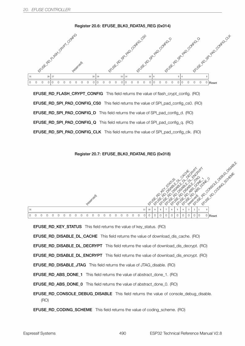
20. EFUSE CONTROLLER
Register 20.6: EFUSE_BLK0_RDATA5_REG (0x014)
EFUSE_R
D_FLA
SH_CRYPT_
CONFIG
0 0 0 0
31 28
(rese
rved)
0 0 0 0 0 0 0 0
27 20
EFUSE_R
D_SPI_P
AD_CONFIG
_CS0
0 0 0 0 0
19 15
EFUSE_R
D_SPI_P
AD_CONFIG
_D
0 0 0 0 0
14 10
EFUSE_R
D_SPI_P
AD_CONFIG
_Q
0 0 0 0 0
9 5
EFUSE_R
D_SPI_P
AD_CONFIG
_CLK
0 0 0 0 0
4 0
Reset
EFUSE_RD_FLASH_CRYPT_CONFIG This field returns the value of flash_crypt_config. (RO)
EFUSE_RD_SPI_PAD_CONFIG_CS0 This field returns the value of SPI_pad_config_cs0. (RO)
EFUSE_RD_SPI_PAD_CONFIG_D This field returns the value of SPI_pad_config_d. (RO)
EFUSE_RD_SPI_PAD_CONFIG_Q This field returns the value of SPI_pad_config_q. (RO)
EFUSE_RD_SPI_PAD_CONFIG_CLK This field returns the value of SPI_pad_config_clk. (RO)
Register 20.7: EFUSE_BLK0_RDATA6_REG (0x018)
(rese
rved)
0 0 0 0 0 0 0 0 0 0 0 0 0 0 0 0 0 0 0 0 0
31 11
EFUSE_R
D_KEY_S
TATU
S
0
10
EFUSE_R
D_DIS
ABLE_D
L_CACHE
0
9
EFUSE_R
D_DIS
ABLE_D
L_DECRYPT
0
8
EFUSE_R
D_DIS
ABLE_D
L_ENCRYPT
0
7
EFUSE_R
D_DIS
ABLE_J
TAG
0
6
EFUSE_R
D_ABS_D
ONE_1
0
5
EFUSE_R
D_ABS_D
ONE_0
0
4
(rese
rved)
0
3
EFUSE_R
D_CONSOLE
_DEBUG_D
ISABLE
0
2
EFUSE_R
D_CODIN
G_SCHEM
E
0 0
1 0
Reset
EFUSE_RD_KEY_STATUS This field returns the value of key_status. (RO)
EFUSE_RD_DISABLE_DL_CACHE This field returns the value of download_dis_cache. (RO)
EFUSE_RD_DISABLE_DL_DECRYPT This field returns the value of download_dis_decrypt. (RO)
EFUSE_RD_DISABLE_DL_ENCRYPT This field returns the value of download_dis_encrypt. (RO)
EFUSE_RD_DISABLE_JTAG This field returns the value of JTAG_disable. (RO)
EFUSE_RD_ABS_DONE_1 This field returns the value of abstract_done_1. (RO)
EFUSE_RD_ABS_DONE_0 This field returns the value of abstract_done_0. (RO)
EFUSE_RD_CONSOLE_DEBUG_DISABLE This field returns the value of console_debug_disable.
(RO)
EFUSE_RD_CODING_SCHEME This field returns the value of coding_scheme. (RO)
Espressif Systems 490 ESP32 Technical Reference Manual V2.8
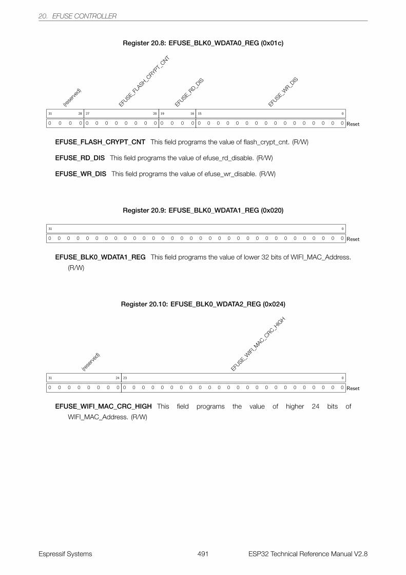
20. EFUSE CONTROLLER
Register 20.8: EFUSE_BLK0_WDATA0_REG (0x01c)
(rese
rved)
0 0 0 0
31 28
EFUSE_F
LASH_C
RYPT_CNT
0 0 0 0 0 0 0 0
27 20
EFUSE_R
D_DIS
0 0 0 0
19 16
EFUSE_W
R_DIS
0 0 0 0 0 0 0 0 0 0 0 0 0 0 0 0
15 0
Reset
EFUSE_FLASH_CRYPT_CNT This field programs the value of flash_crypt_cnt. (R/W)
EFUSE_RD_DIS This field programs the value of efuse_rd_disable. (R/W)
EFUSE_WR_DIS This field programs the value of efuse_wr_disable. (R/W)
Register 20.9: EFUSE_BLK0_WDATA1_REG (0x020)
0 0 0 0 0 0 0 0 0 0 0 0 0 0 0 0 0 0 0 0 0 0 0 0 0 0 0 0 0 0 0 0
31 0
Reset
EFUSE_BLK0_WDATA1_REG This field programs the value of lower 32 bits of WIFI_MAC_Address.
(R/W)
Register 20.10: EFUSE_BLK0_WDATA2_REG (0x024)
(rese
rved)
0 0 0 0 0 0 0 0
31 24
EFUSE_W
IFI_M
AC_CRC_H
IGH
0 0 0 0 0 0 0 0 0 0 0 0 0 0 0 0 0 0 0 0 0 0 0 0
23 0
Reset
EFUSE_WIFI_MAC_CRC_HIGH This field programs the value of higher 24 bits of
WIFI_MAC_Address. (R/W)
Espressif Systems 491 ESP32 Technical Reference Manual V2.8
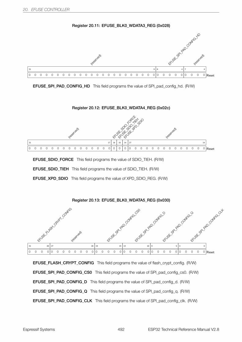
20. EFUSE CONTROLLER
Register 20.11: EFUSE_BLK0_WDATA3_REG (0x028)
(rese
rved)
0 0 0 0 0 0 0 0 0 0 0 0 0 0 0 0 0 0 0 0 0 0 0
31 9
EFUSE_S
PI_PAD_C
ONFIG_H
D
0 0 0 0 0
8 4
(rese
rved)
0 0 0 0
7 4
Reset
EFUSE_SPI_PAD_CONFIG_HD This field programs the value of SPI_pad_config_hd. (R/W)
Register 20.12: EFUSE_BLK0_WDATA4_REG (0x02c)
(rese
rved)
0 0 0 0 0 0 0 0 0 0 0 0 0 0 0
31 17
EFUSE_S
DIO_F
ORCE
0
16
EFUSE_S
DIO_T
IEH
0
15
EFUSE_X
PD_SDIO
0
14
(rese
rved)
0 0 0 0 0 0 0 0 0 0 0 0 0 0
27 14
Reset
EFUSE_SDIO_FORCE This field programs the value of SDIO_TIEH. (R/W)
EFUSE_SDIO_TIEH This field programs the value of SDIO_TIEH. (R/W)
EFUSE_XPD_SDIO This field programs the value of XPD_SDIO_REG. (R/W)
Register 20.13: EFUSE_BLK0_WDATA5_REG (0x030)
EFUSE_F
LASH_C
RYPT_CONFIG
0 0 0 0
31 28
(rese
rved)
0 0 0 0 0 0 0 0
27 20
EFUSE_S
PI_PAD_C
ONFIG_C
S0
0 0 0 0 0
19 15
EFUSE_S
PI_PAD_C
ONFIG_D
0 0 0 0 0
14 10
EFUSE_S
PI_PAD_C
ONFIG_Q
0 0 0 0 0
9 5
EFUSE_S
PI_PAD_C
ONFIG_C
LK
0 0 0 0 0
4 0
Reset
EFUSE_FLASH_CRYPT_CONFIG This field programs the value of flash_crypt_config. (R/W)
EFUSE_SPI_PAD_CONFIG_CS0 This field programs the value of SPI_pad_config_cs0. (R/W)
EFUSE_SPI_PAD_CONFIG_D This field programs the value of SPI_pad_config_d. (R/W)
EFUSE_SPI_PAD_CONFIG_Q This field programs the value of SPI_pad_config_q. (R/W)
EFUSE_SPI_PAD_CONFIG_CLK This field programs the value of SPI_pad_config_clk. (R/W)
Espressif Systems 492 ESP32 Technical Reference Manual V2.8
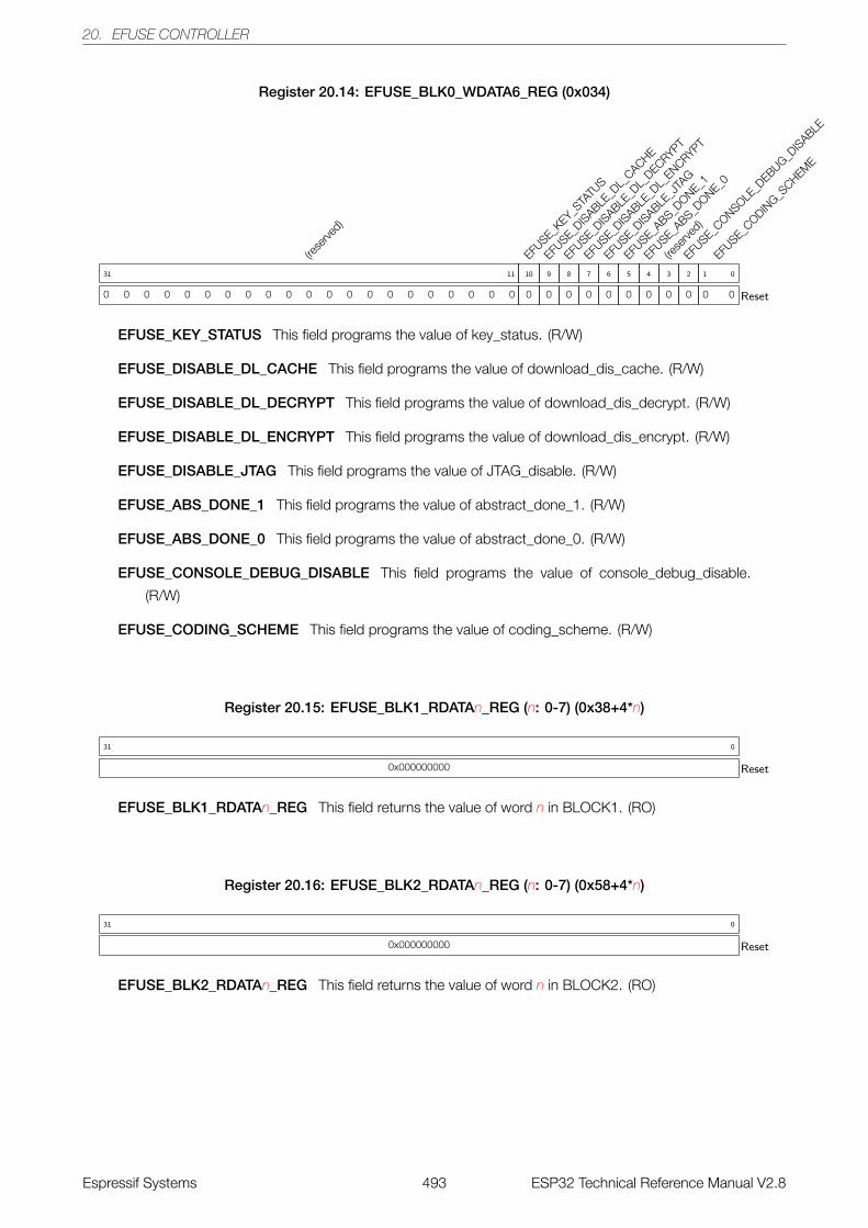
20. EFUSE CONTROLLER
Register 20.14: EFUSE_BLK0_WDATA6_REG (0x034)
(rese
rved)
0 0 0 0 0 0 0 0 0 0 0 0 0 0 0 0 0 0 0 0 0
31 11
EFUSE_K
EY_STA
TUS
0
10
EFUSE_D
ISABLE
_DL_
CACHE
0
9
EFUSE_D
ISABLE
_DL_
DECRYPT
0
8
EFUSE_D
ISABLE
_DL_
ENCRYPT
0
7
EFUSE_D
ISABLE
_JTA
G
0
6
EFUSE_A
BS_DONE_1
0
5
EFUSE_A
BS_DONE_0
0
4
(rese
rved)
0
3
EFUSE_C
ONSOLE_D
EBUG_DIS
ABLE
0
2
EFUSE_C
ODING_S
CHEME
0 0
1 0
Reset
EFUSE_KEY_STATUS This field programs the value of key_status. (R/W)
EFUSE_DISABLE_DL_CACHE This field programs the value of download_dis_cache. (R/W)
EFUSE_DISABLE_DL_DECRYPT This field programs the value of download_dis_decrypt. (R/W)
EFUSE_DISABLE_DL_ENCRYPT This field programs the value of download_dis_encrypt. (R/W)
EFUSE_DISABLE_JTAG This field programs the value of JTAG_disable. (R/W)
EFUSE_ABS_DONE_1 This field programs the value of abstract_done_1. (R/W)
EFUSE_ABS_DONE_0 This field programs the value of abstract_done_0. (R/W)
EFUSE_CONSOLE_DEBUG_DISABLE This field programs the value of console_debug_disable.
(R/W)
EFUSE_CODING_SCHEME This field programs the value of coding_scheme. (R/W)
Register 20.15: EFUSE_BLK1_RDATAn_REG (n: 0-7) (0x38+4*n)
0x000000000
31 0
Reset
EFUSE_BLK1_RDATAn_REG This field returns the value of word n in BLOCK1. (RO)
Register 20.16: EFUSE_BLK2_RDATAn_REG (n: 0-7) (0x58+4*n)
0x000000000
31 0
Reset
EFUSE_BLK2_RDATAn_REG This field returns the value of word n in BLOCK2. (RO)
Espressif Systems 493 ESP32 Technical Reference Manual V2.8
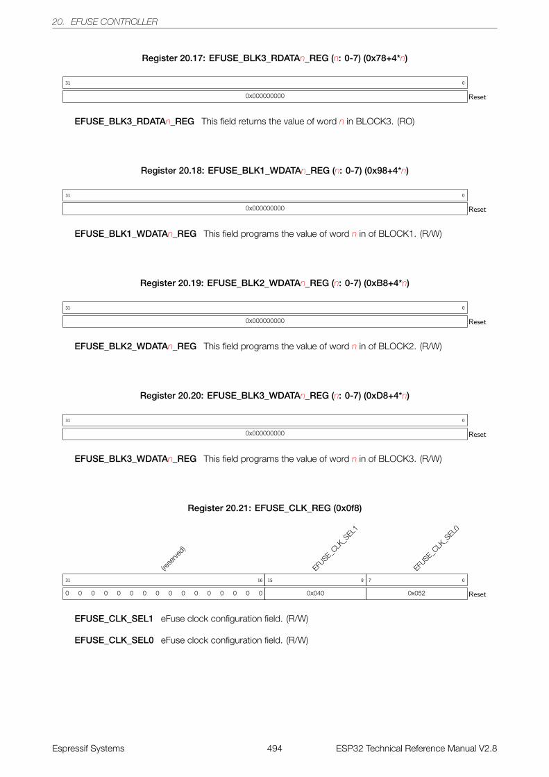
20. EFUSE CONTROLLER
Register 20.17: EFUSE_BLK3_RDATAn_REG (n: 0-7) (0x78+4*n)
0x000000000
31 0
Reset
EFUSE_BLK3_RDATAn_REG This field returns the value of word n in BLOCK3. (RO)
Register 20.18: EFUSE_BLK1_WDATAn_REG (n: 0-7) (0x98+4*n)
0x000000000
31 0
Reset
EFUSE_BLK1_WDATAn_REG This field programs the value of word n in of BLOCK1. (R/W)
Register 20.19: EFUSE_BLK2_WDATAn_REG (n: 0-7) (0xB8+4*n)
0x000000000
31 0
Reset
EFUSE_BLK2_WDATAn_REG This field programs the value of word n in of BLOCK2. (R/W)
Register 20.20: EFUSE_BLK3_WDATAn_REG (n: 0-7) (0xD8+4*n)
0x000000000
31 0
Reset
EFUSE_BLK3_WDATAn_REG This field programs the value of word n in of BLOCK3. (R/W)
Register 20.21: EFUSE_CLK_REG (0x0f8)
(rese
rved)
0 0 0 0 0 0 0 0 0 0 0 0 0 0 0 0
31 16
EFUSE_C
LK_S
EL1
0x040
15 8
EFUSE_C
LK_S
EL0
0x052
7 0
Reset
EFUSE_CLK_SEL1 eFuse clock configuration field. (R/W)
EFUSE_CLK_SEL0 eFuse clock configuration field. (R/W)
Espressif Systems 494 ESP32 Technical Reference Manual V2.8
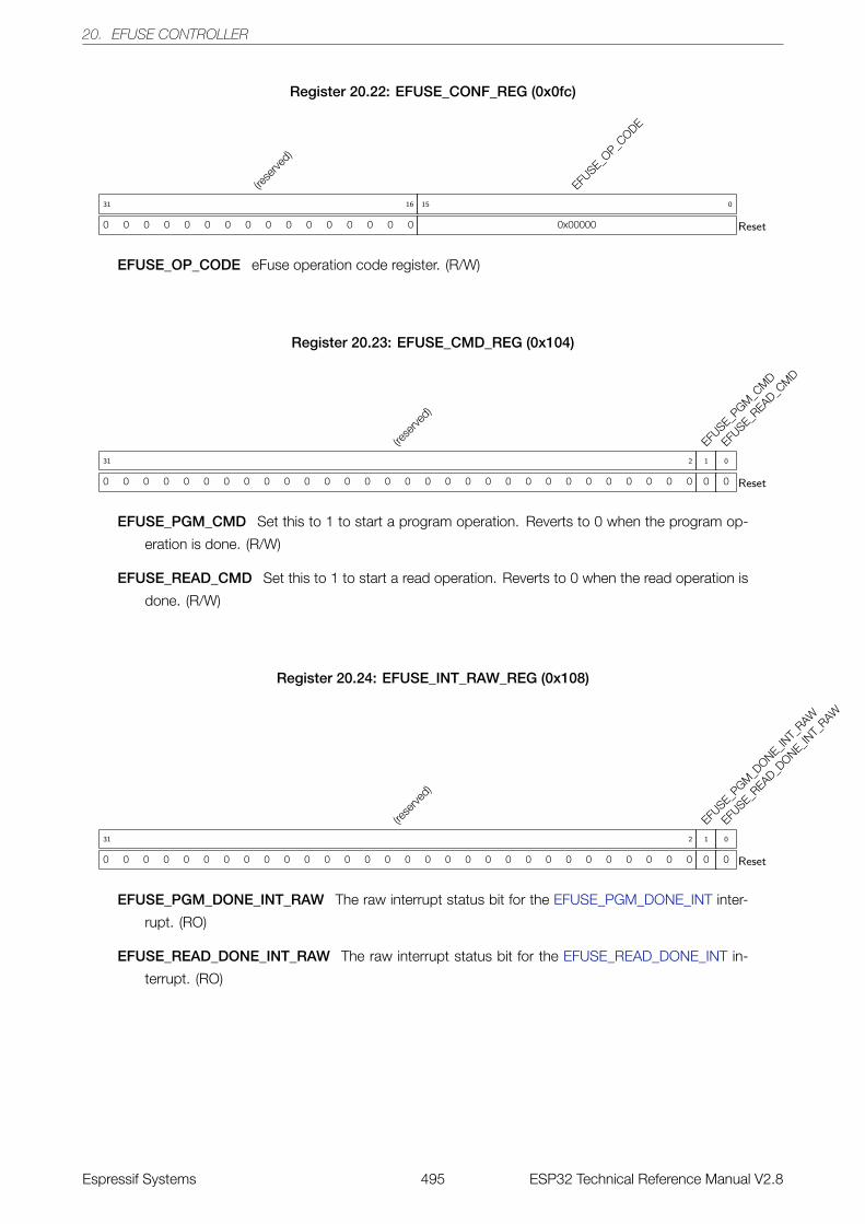
20. EFUSE CONTROLLER
Register 20.22: EFUSE_CONF_REG (0x0fc)
(rese
rved)
0 0 0 0 0 0 0 0 0 0 0 0 0 0 0 0
31 16
EFUSE_O
P_CODE
0x00000
15 0
Reset
EFUSE_OP_CODE eFuse operation code register. (R/W)
Register 20.23: EFUSE_CMD_REG (0x104)
(rese
rved)
0 0 0 0 0 0 0 0 0 0 0 0 0 0 0 0 0 0 0 0 0 0 0 0 0 0 0 0 0 0
31 2
EFUSE_P
GM_C
MD
0
1
EFUSE_R
EAD_CM
D
0
0
Reset
EFUSE_PGM_CMD Set this to 1 to start a program operation. Reverts to 0 when the program op-
eration is done. (R/W)
EFUSE_READ_CMD Set this to 1 to start a read operation. Reverts to 0 when the read operation is
done. (R/W)
Register 20.24: EFUSE_INT_RAW_REG (0x108)
(rese
rved)
0 0 0 0 0 0 0 0 0 0 0 0 0 0 0 0 0 0 0 0 0 0 0 0 0 0 0 0 0 0
31 2
EFUSE_P
GM_D
ONE_INT_
RAW
0
1
EFUSE_R
EAD_DONE_IN
T_RAW
0
0
Reset
EFUSE_PGM_DONE_INT_RAW The raw interrupt status bit for the EFUSE_PGM_DONE_INT inter-
rupt. (RO)
EFUSE_READ_DONE_INT_RAW The raw interrupt status bit for the EFUSE_READ_DONE_INT in-
terrupt. (RO)
Espressif Systems 495 ESP32 Technical Reference Manual V2.8
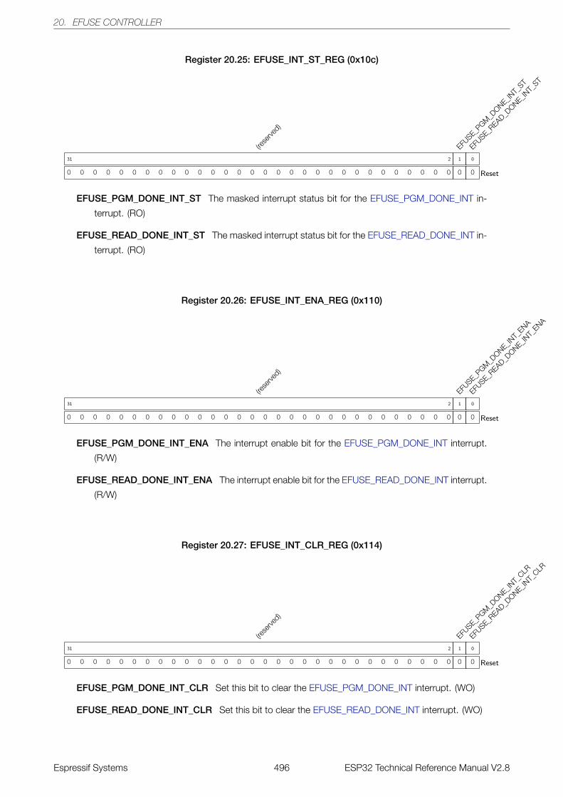
20. EFUSE CONTROLLER
Register 20.25: EFUSE_INT_ST_REG (0x10c)
(rese
rved)
0 0 0 0 0 0 0 0 0 0 0 0 0 0 0 0 0 0 0 0 0 0 0 0 0 0 0 0 0 0
31 2
EFUSE_P
GM_D
ONE_INT_
ST
0
1
EFUSE_R
EAD_DONE_IN
T_ST
0
0
Reset
EFUSE_PGM_DONE_INT_ST The masked interrupt status bit for the EFUSE_PGM_DONE_INT in-
terrupt. (RO)
EFUSE_READ_DONE_INT_ST The masked interrupt status bit for the EFUSE_READ_DONE_INT in-
terrupt. (RO)
Register 20.26: EFUSE_INT_ENA_REG (0x110)
(rese
rved)
0 0 0 0 0 0 0 0 0 0 0 0 0 0 0 0 0 0 0 0 0 0 0 0 0 0 0 0 0 0
31 2
EFUSE_P
GM_D
ONE_INT_
ENA
0
1
EFUSE_R
EAD_DONE_IN
T_ENA
0
0
Reset
EFUSE_PGM_DONE_INT_ENA The interrupt enable bit for the EFUSE_PGM_DONE_INT interrupt.
(R/W)
EFUSE_READ_DONE_INT_ENA The interrupt enable bit for the EFUSE_READ_DONE_INT interrupt.
(R/W)
Register 20.27: EFUSE_INT_CLR_REG (0x114)
(rese
rved)
0 0 0 0 0 0 0 0 0 0 0 0 0 0 0 0 0 0 0 0 0 0 0 0 0 0 0 0 0 0
31 2
EFUSE_P
GM_D
ONE_INT_
CLR
0
1
EFUSE_R
EAD_DONE_IN
T_CLR
0
0
Reset
EFUSE_PGM_DONE_INT_CLR Set this bit to clear the EFUSE_PGM_DONE_INT interrupt. (WO)
EFUSE_READ_DONE_INT_CLR Set this bit to clear the EFUSE_READ_DONE_INT interrupt. (WO)
Espressif Systems 496 ESP32 Technical Reference Manual V2.8
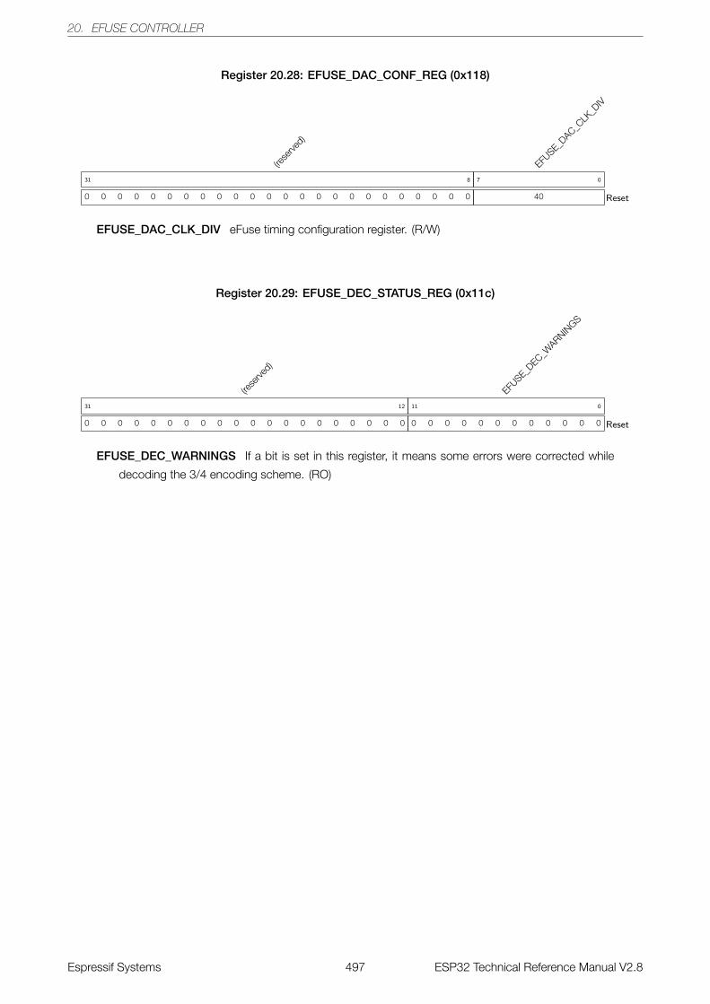
20. EFUSE CONTROLLER
Register 20.28: EFUSE_DAC_CONF_REG (0x118)
(rese
rved)
0 0 0 0 0 0 0 0 0 0 0 0 0 0 0 0 0 0 0 0 0 0 0 0
31 8
EFUSE_D
AC_CLK
_DIV
40
7 0
Reset
EFUSE_DAC_CLK_DIV eFuse timing configuration register. (R/W)
Register 20.29: EFUSE_DEC_STATUS_REG (0x11c)
(rese
rved)
0 0 0 0 0 0 0 0 0 0 0 0 0 0 0 0 0 0 0 0
31 12
EFUSE_D
EC_WARNIN
GS
0 0 0 0 0 0 0 0 0 0 0 0
11 0
Reset
EFUSE_DEC_WARNINGS If a bit is set in this register, it means some errors were corrected while
decoding the 3/4 encoding scheme. (RO)
Espressif Systems 497 ESP32 Technical Reference Manual V2.8
21. AES ACCELERATOR
21. AES Accelerator
21.1 Introduction
The AES Accelerator speeds up AES operations significantly, compared to AES algorithms implemented solely in
software. The AES Accelerator supports six algorithms of FIPS PUB 197, specifically AES-128, AES-192 and
AES-256 encryption and decryption.
21.2 Features
• Supports AES-128 encryption and decryption
• Supports AES-192 encryption and decryption
• Supports AES-256 encryption and decryption
• Supports four variations of key endianness and four variations of text endianness
21.3 Functional Description
21.3.1 AES Algorithm Operations
The AES Accelerator supports six algorithms of FIPS PUB 197, specifically AES-128, AES-192 and AES-256
encryption and decryption. The AES_MODE_REG register can be configured to different values to enable
different algorithm operations, as shown in Table 83.
Table 83: Operation Mode
AES_MODE_REG[2:0] Operation
0 AES-128 Encryption
1 AES-192 Encryption
2 AES-256 Encryption
4 AES-128 Decryption
5 AES-192 Decryption
6 AES-256 Decryption
21.3.2 Key, Plaintext and Ciphertext
The encryption or decryption key is stored in AES_KEY_n_REG, which is a set of eight 32-bit registers. For
AES-128 encryption/decryption, the 128-bit key is stored in AES_KEY_0_REG ~ AES_KEY_3_REG. For
AES-192 encryption/decryption, the 192-bit key is stored in AES_KEY_0_REG ~ AES_KEY_5_REG. For
AES-256 encryption/decryption, the 256-bit key is stored in AES_KEY_0_REG ~ AES_KEY_7_REG.
Plaintext and ciphertext is stored in the AES_TEXT_m_REG registers. There are four 32-bit registers. To enable
AES-128/192/256 encryption, initialize the AES_TEXT_m_REG registers with plaintext before encryption. When
encryption is finished, the AES Accelerator will store back the resulting ciphertext in the AES_TEXT_m_REG
registers. To enable AES-128/192/256 decryption, initialize the AES_TEXT_m_REG registers with ciphertext
before decryption. When decryption is finished, the AES Accelerator will store back the resulting plaintext in the
AES_TEXT_m_REG registers.
Espressif Systems 498 ESP32 Technical Reference Manual V2.8
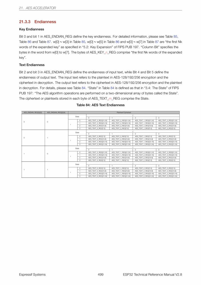
21. AES ACCELERATOR
21.3.3 Endianness
Key Endianness
Bit 0 and bit 1 in AES_ENDIAN_REG define the key endianness. For detailed information, please see Table 85,
Table 86 and Table 87. w[0] ~ w[3] in Table 85, w[0] ~ w[5] in Table 86 and w[0] ~ w[7] in Table 87 are “the first Nk
words of the expanded key” as specified in “5.2: Key Expansion” of FIPS PUB 197. “Column Bit” specifies the
bytes in the word from w[0] to w[7]. The bytes of AES_KEY_n_REG comprise “the first Nk words of the expanded
key”.
Text Endianness
Bit 2 and bit 3 in AES_ENDIAN_REG define the endianness of input text, while Bit 4 and Bit 5 define the
endianness of output text. The input text refers to the plaintext in AES-128/192/256 encryption and the
ciphertext in decryption. The output text refers to the ciphertext in AES-128/192/256 encryption and the plaintext
in decryption. For details, please see Table 84. “State” in Table 84 is defined as that in “3.4: The State” of FIPS
PUB 197: “The AES algorithm operations are performed on a two-dimensional array of bytes called the State”.
The ciphertext or plaintexts stored in each byte of AES_TEXT_m_REG comprise the State.
Table 84: AES Text Endianness
AES_ENDIAN_REG[3]/[5] AES_ENDIAN_REG[2]/[4] Plaintext/Ciphertext
0 0
Statec
0 1 2 3
r
0 AES_TEXT_3_REG[31:24] AES_TEXT_2_REG[31:24] AES_TEXT_1_REG[31:24] AES_TEXT_0_REG[31:24]
1 AES_TEXT_3_REG[23:16] AES_TEXT_2_REG[23:16] AES_TEXT_1_REG[23:16] AES_TEXT_0_REG[23:16]
2 AES_TEXT_3_REG[15:8] AES_TEXT_2_REG[15:8] AES_TEXT_1_REG[15:8] AES_TEXT_0_REG[15:8]
3 AES_TEXT_3_REG[7:0] AES_TEXT_2_REG[7:0] AES_TEXT_1_REG[7:0] AES_TEXT_0_REG[7:0]
0 1
Statec
0 1 2 3
r
0 AES_TEXT_3_REG[7:0] AES_TEXT_2_REG[7:0] AES_TEXT_1_REG[7:0] AES_TEXT_0_REG[7:0]
1 AES_TEXT_3_REG[15:8] AES_TEXT_2_REG[15:8] AES_TEXT_1_REG[15:8] AES_TEXT_0_REG[15:8]
2 AES_TEXT_3_REG[23:16] AES_TEXT_2_REG[23:16] AES_TEXT_1_REG[23:16] AES_TEXT_0_REG[23:16]
3 AES_TEXT_3_REG[31:24] AES_TEXT_2_REG[31:24] AES_TEXT_1_REG[31:24] AES_TEXT_0_REG[31:24]
1 0
Statec
0 1 2 3
r
0 AES_TEXT_0_REG[31:24] AES_TEXT_1_REG[31:24] AES_TEXT_2_REG[31:24] AES_TEXT_3_REG[31:24]
1 AES_TEXT_0_REG[23:16] AES_TEXT_1_REG[23:16] AES_TEXT_2_REG[23:16] AES_TEXT_3_REG[23:16]
2 AES_TEXT_0_REG[15:8] AES_TEXT_1_REG[15:8] AES_TEXT_2_REG[15:8] AES_TEXT_3_REG[15:8]
3 AES_TEXT_0_REG[7:0] AES_TEXT_1_REG[7:0] AES_TEXT_2_REG[7:0] AES_TEXT_3_REG[7:0]
1 1
Statec
0 1 2 3
r
0 AES_TEXT_0_REG[7:0] AES_TEXT_1_REG[7:0] AES_TEXT_2_REG[7:0] AES_TEXT_3_REG[7:0]
1 AES_TEXT_0_REG[15:8] AES_TEXT_1_REG[15:8] AES_TEXT_2_REG[15:8] AES_TEXT_3_REG[15:8]
2 AES_TEXT_0_REG[23:16] AES_TEXT_1_REG[23:16] AES_TEXT_2_REG[23:16] AES_TEXT_3_REG[23:16]
3 AES_TEXT_0_REG[31:24] AES_TEXT_1_REG[31:24] AES_TEXT_2_REG[31:24] AES_TEXT_3_REG[31:24]
Espressif Systems 499 ESP32 Technical Reference Manual V2.8

21.AES
ACCELER
ATO
RTable 85: AES-128 Key Endianness
AES_ENDIAN_REG[1] AES_ENDIAN_REG[0] Bit w[0] w[1] w[2] w[3]
0 0
[31:24] AES_KEY_3_REG[31:24] AES_KEY_2_REG[31:24] AES_KEY_1_REG[31:24] AES_KEY_0_REG[31:24]
[23:16] AES_KEY_3_REG[23:16] AES_KEY_2_REG[23:16] AES_KEY_1_REG[23:16] AES_KEY_0_REG[23:16]
[15:8] AES_KEY_3_REG[15:8] AES_KEY_2_REG[15:8] AES_KEY_1_REG[15:8] AES_KEY_0_REG[15:8]
[7:0] AES_KEY_3_REG[7:0] AES_KEY_2_REG[7:0] AES_KEY_1_REG[7:0] AES_KEY_0_REG[7:0]
0 1
[31:24] AES_KEY_3_REG[7:0] AES_KEY_2_REG[7:0] AES_KEY_1_REG[7:0] AES_KEY_0_REG[7:0]
[23:16] AES_KEY_3_REG[15:8] AES_KEY_2_REG[15:8] AES_KEY_1_REG[15:8] AES_KEY_0_REG[15:8]
[15:8] AES_KEY_3_REG[23:16] AES_KEY_2_REG[23:16] AES_KEY_1_REG[23:16] AES_KEY_0_REG[23:16]
[7:0] AES_KEY_3_REG[31:24] AES_KEY_2_REG[31:24] AES_KEY_1_REG[31:24] AES_KEY_0_REG[31:24]
1 0
[31:24] AES_KEY_0_REG[31:24] AES_KEY_1_REG[31:24] AES_KEY_2_REG[31:24] AES_KEY_3_REG[31:24]
[23:16] AES_KEY_0_REG[23:16] AES_KEY_1_REG[23:16] AES_KEY_2_REG[23:16] AES_KEY_3_REG[23:16]
[15:8] AES_KEY_0_REG[15:8] AES_KEY_1_REG[15:8] AES_KEY_2_REG[15:8] AES_KEY_3_REG[15:8]
[7:0] AES_KEY_0_REG[7:0] AES_KEY_1_REG[7:0] AES_KEY_2_REG[7:0] AES_KEY_3_REG[7:0]
1 1
[31:24] AES_KEY_0_REG[7:0] AES_KEY_1_REG[7:0] AES_KEY_2_REG[7:0] AES_KEY_3_REG[7:0]
[23:16] AES_KEY_0_REG[15:8] AES_KEY_1_REG[15:8] AES_KEY_2_REG[15:8] AES_KEY_3_REG[15:8]
[15:8] AES_KEY_0_REG[23:16] AES_KEY_1_REG[23:16] AES_KEY_2_REG[23:16] AES_KEY_3_REG[23:16]
[7:0] AES_KEY_0_REG[31:24] AES_KEY_1_REG[31:24] AES_KEY_2_REG[31:24] AES_KEY_3_REG[31:24]
Table 86: AES-192 Key Endianness
AES_ENDIAN_REG[1] AES_ENDIAN_REG[0] Bit w[0] w[1] w[2] w[3] w[4] w[5]
0 0
[31:24] AES_KEY_5_REG[31:24] AES_KEY_4_REG[31:24] AES_KEY_3_REG[31:24] AES_KEY_2_REG[31:24] AES_KEY_1_REG[31:24] AES_KEY_0_REG[31:24]
[23:16] AES_KEY_5_REG[23:16] AES_KEY_4_REG[23:16] AES_KEY_3_REG[23:16] AES_KEY_2_REG[23:16] AES_KEY_1_REG[23:16] AES_KEY_0_REG[23:16]
[15:8] AES_KEY_5_REG[15:8] AES_KEY_4_REG[15:8] AES_KEY_3_REG[15:8] AES_KEY_2_REG[15:8] AES_KEY_1_REG[15:8] AES_KEY_0_REG[15:8]
[7:0] AES_KEY_5_REG[7:0] AES_KEY_4_REG[7:0] AES_KEY_3_REG[7:0] AES_KEY_2_REG[7:0] AES_KEY_1_REG[7:0] AES_KEY_0_REG[7:0]
0 1
[31:24] AES_KEY_5_REG[7:0] AES_KEY_4_REG[7:0] AES_KEY_3_REG[7:0] AES_KEY_2_REG[7:0] AES_KEY_1_REG[7:0] AES_KEY_0_REG[7:0]
[23:16] AES_KEY_5_REG[15:8] AES_KEY_4_REG[15:8] AES_KEY_3_REG[15:8] AES_KEY_2_REG[15:8] AES_KEY_1_REG[15:8] AES_KEY_0_REG[15:8]
[15:8] AES_KEY_5_REG[23:16] AES_KEY_4_REG[23:16] AES_KEY_3_REG[23:16] AES_KEY_2_REG[23:16] AES_KEY_1_REG[23:16] AES_KEY_0_REG[23:16]
[7:0] AES_KEY_5_REG[31:24] AES_KEY_4_REG[31:24] AES_KEY_3_REG[31:24] AES_KEY_2_REG[31:24] AES_KEY_1_REG[31:24] AES_KEY_0_REG[31:24]
1 0
[31:24] AES_KEY_0_REG[31:24] AES_KEY_1_REG[31:24] AES_KEY_2_REG[31:24] AES_KEY_3_REG[31:24] AES_KEY_4_REG[31:24] AES_KEY_5_REG[31:24]
[23:16] AES_KEY_0_REG[23:16] AES_KEY_1_REG[23:16] AES_KEY_2_REG[23:16] AES_KEY_3_REG[23:16] AES_KEY_4_REG[23:16] AES_KEY_5_REG[23:16]
[15:8] AES_KEY_0_REG[15:8] AES_KEY_1_REG[15:8] AES_KEY_2_REG[15:8] AES_KEY_3_REG[15:8] AES_KEY_4_REG[15:8] AES_KEY_5_REG[15:8]
[7:0] AES_KEY_0_REG[7:0] AES_KEY_1_REG[7:0] AES_KEY_2_REG[7:0] AES_KEY_3_REG[7:0] AES_KEY_4_REG[7:0] AES_KEY_5_REG[7:0]
1 1
[31:24] AES_KEY_0_REG[7:0] AES_KEY_1_REG[7:0] AES_KEY_2_REG[7:0] AES_KEY_3_REG[7:0] AES_KEY_4_REG[7:0] AES_KEY_5_REG[7:0]
[23:16] AES_KEY_0_REG[15:8] AES_KEY_1_REG[15:8] AES_KEY_2_REG[15:8] AES_KEY_3_REG[15:8] AES_KEY_4_REG[15:8] AES_KEY_5_REG[15:8]
[15:8] AES_KEY_0_REG[23:16] AES_KEY_1_REG[23:16] AES_KEY_2_REG[23:16] AES_KEY_3_REG[23:16] AES_KEY_4_REG[23:16] AES_KEY_5_REG[23:16]
[7:0] AES_KEY_0_REG[31:24] AES_KEY_1_REG[31:24] AES_KEY_2_REG[31:24] AES_KEY_3_REG[31:24] AES_KEY_4_REG[31:24] AES_KEY_5_REG[31:24]
Table 87: AES-256 Key Endianness
AES_ENDIAN_REG[1] AES_ENDIAN_REG[0] Bit w[0] w[1] w[2] w[3] w[4] w[5] w[6] w[7]
0 0
[31:24] AES_KEY_7_REG[31:24] AES_KEY_6_REG[31:24] AES_KEY_5_REG[31:24] AES_KEY_4_REG[31:24] AES_KEY_3_REG[31:24] AES_KEY_2_REG[31:24] AES_KEY_1_REG[31:24] AES_KEY_0_REG[31:24]
[23:16] AES_KEY_7_REG[23:16] AES_KEY_6_REG[23:16] AES_KEY_5_REG[23:16] AES_KEY_4_REG[23:16] AES_KEY_3_REG[23:16] AES_KEY_2_REG[23:16] AES_KEY_1_REG[23:16] AES_KEY_0_REG[23:16]
[15:8] AES_KEY_7_REG[15:8] AES_KEY_6_REG[15:8] AES_KEY_5_REG[15:8] AES_KEY_4_REG[15:8] AES_KEY_3_REG[15:8] AES_KEY_2_REG[15:8] AES_KEY_1_REG[15:8] AES_KEY_0_REG[15:8]
[7:0] AES_KEY_7_REG[7:0] AES_KEY_6_REG[7:0] AES_KEY_5_REG[7:0] AES_KEY_4_REG[7:0] AES_KEY_3_REG[7:0] AES_KEY_2_REG[7:0] AES_KEY_1_REG[7:0] AES_KEY_0_REG[7:0]
0 1
[31:24] AES_KEY_7_REG[7:0] AES_KEY_6_REG[7:0] AES_KEY_5_REG[7:0] AES_KEY_4_REG[7:0] AES_KEY_3_REG[7:0] AES_KEY_2_REG[7:0] AES_KEY_1_REG[7:0] AES_KEY_0_REG[7:0]
[23:16] AES_KEY_7_REG[15:8] AES_KEY_6_REG[15:8] AES_KEY_5_REG[15:8] AES_KEY_4_REG[15:8] AES_KEY_3_REG[15:8] AES_KEY_2_REG[15:8] AES_KEY_1_REG[15:8] AES_KEY_0_REG[15:8]
[15:8] AES_KEY_7_REG[23:16] AES_KEY_6_REG[23:16] AES_KEY_5_REG[23:16] AES_KEY_4_REG[23:16] AES_KEY_3_REG[23:16] AES_KEY_2_REG[23:16] AES_KEY_1_REG[23:16] AES_KEY_0_REG[23:16]
[7:0] AES_KEY_7_REG[31:24] AES_KEY_6_REG[31:24] AES_KEY_5_REG[31:24] AES_KEY_4_REG[31:24] AES_KEY_3_REG[31:24] AES_KEY_2_REG[31:24] AES_KEY_1_REG[31:24] AES_KEY_0_REG[31:24]
1 0
[31:24] AES_KEY_0_REG[31:24] AES_KEY_1_REG[31:24] AES_KEY_2_REG[31:24] AES_KEY_3_REG[31:24] AES_KEY_4_REG[31:24] AES_KEY_5_REG[31:24] AES_KEY_6_REG[31:24] AES_KEY_7_REG[31:24]
[23:16] AES_KEY_0_REG[23:16] AES_KEY_1_REG[23:16] AES_KEY_2_REG[23:16] AES_KEY_3_REG[23:16] AES_KEY_4_REG[23:16] AES_KEY_5_REG[23:16] AES_KEY_6_REG[23:16] AES_KEY_7_REG[23:16]
[15:8] AES_KEY_0_REG[15:8] AES_KEY_1_REG[15:8] AES_KEY_2_REG[15:8] AES_KEY_3_REG[15:8] AES_KEY_4_REG[15:8] AES_KEY_5_REG[15:8] AES_KEY_6_REG[15:8] AES_KEY_7_REG[15:8]
[7:0] AES_KEY_0_REG[7:0] AES_KEY_1_REG[7:0] AES_KEY_2_REG[7:0] AES_KEY_3_REG[7:0] AES_KEY_4_REG[7:0] AES_KEY_5_REG[7:0] AES_KEY_6_REG[7:0] AES_KEY_7_REG[7:0]
1 1
[31:24] AES_KEY_0_REG[7:0] AES_KEY_1_REG[7:0] AES_KEY_2_REG[7:0] AES_KEY_3_REG[7:0] AES_KEY_4_REG[7:0] AES_KEY_5_REG[7:0] AES_KEY_6_REG[7:0] AES_KEY_7_REG[7:0]
[23:16] AES_KEY_0_REG[15:8] AES_KEY_1_REG[15:8] AES_KEY_2_REG[15:8] AES_KEY_3_REG[15:8] AES_KEY_4_REG[15:8] AES_KEY_5_REG[15:8] AES_KEY_6_REG[15:8] AES_KEY_7_REG[15:8]
[15:8] AES_KEY_0_REG[23:16] AES_KEY_1_REG[23:16] AES_KEY_2_REG[23:16] AES_KEY_3_REG[23:16] AES_KEY_4_REG[23:16] AES_KEY_5_REG[23:16] AES_KEY_6_REG[23:16] AES_KEY_7_REG[23:16]
[7:0] AES_KEY_0_REG[31:24] AES_KEY_1_REG[31:24] AES_KEY_2_REG[31:24] AES_KEY_3_REG[31:24] AES_KEY_4_REG[31:24] AES_KEY_5_REG[31:24] AES_KEY_6_REG[31:24] AES_KEY_7_REG[31:24]
EspressifS
ystems
500E
SP
32TechnicalR
eferenceM
anualV2.8

21. AES ACCELERATOR
21.3.4 Encryption and Decryption Operations
Single Operation
1. Initialize AES_MODE_REG, AES_KEY_n_REG, AES_TEXT_m_REG and AES_ENDIAN_REG.
2. Write 1 to AES_START_REG.
3. Wait until AES_IDLE_REG reads 1.
4. Read results from AES_TEXT_m_REG.
Consecutive Operations
Every time an operation is completed, only AES_TEXT_m_REG is modified by the AES Accelerator. Initialization
can, therefore, be simplified in a series of consecutive operations.
1. Update contents of AES_MODE_REG, AES_KEY_n_REG and AES_ENDIAN_REG, if required.
2. Load AES_TEXT_m_REG.
3. Write 1 to AES_START_REG.
4. Wait until AES_IDLE_REG reads 1.
5. Read results from AES_TEXT_m_REG.
21.3.5 Speed
The AES Accelerator requires 11 to 15 clock cycles to encrypt a message block, and 21 or 22 clock cycles to
decrypt a message block.
21.4 Register Summary
Name Description Address Access
Configuration registers
AES_MODE_REG Mode of operation of the AES Accelerator 0x3FF01008 R/W
AES_ENDIAN_REG Endianness configuration register 0x3FF01040 R/W
Key registers
AES_KEY_0_REG AES key material register 0 0x3FF01010 R/W
AES_KEY_1_REG AES key material register 1 0x3FF01014 R/W
AES_KEY_2_REG AES key material register 2 0x3FF01018 R/W
AES_KEY_3_REG AES key material register 3 0x3FF0101C R/W
AES_KEY_4_REG AES key material register 4 0x3FF01020 R/W
AES_KEY_5_REG AES key material register 5 0x3FF01024 R/W
AES_KEY_6_REG AES key material register 6 0x3FF01028 R/W
AES_KEY_7_REG AES key material register 7 0x3FF0102C R/W
Encrypted/decrypted data registers
AES_TEXT_0_REG AES encrypted/decrypted data register 0 0x3FF01030 R/W
AES_TEXT_1_REG AES encrypted/decrypted data register 1 0x3FF01034 R/W
AES_TEXT_2_REG AES encrypted/decrypted data register 2 0x3FF01038 R/W
AES_TEXT_3_REG AES encrypted/decrypted data register 3 0x3FF0103C R/W
Control/status registers
Espressif Systems 501 ESP32 Technical Reference Manual V2.8

21. AES ACCELERATOR
Name Description Address Access
AES_START_REG AES operation start control register 0x3FF01000 WO
AES_IDLE_REG AES idle status register 0x3FF01004 RO
Espressif Systems 502 ESP32 Technical Reference Manual V2.8
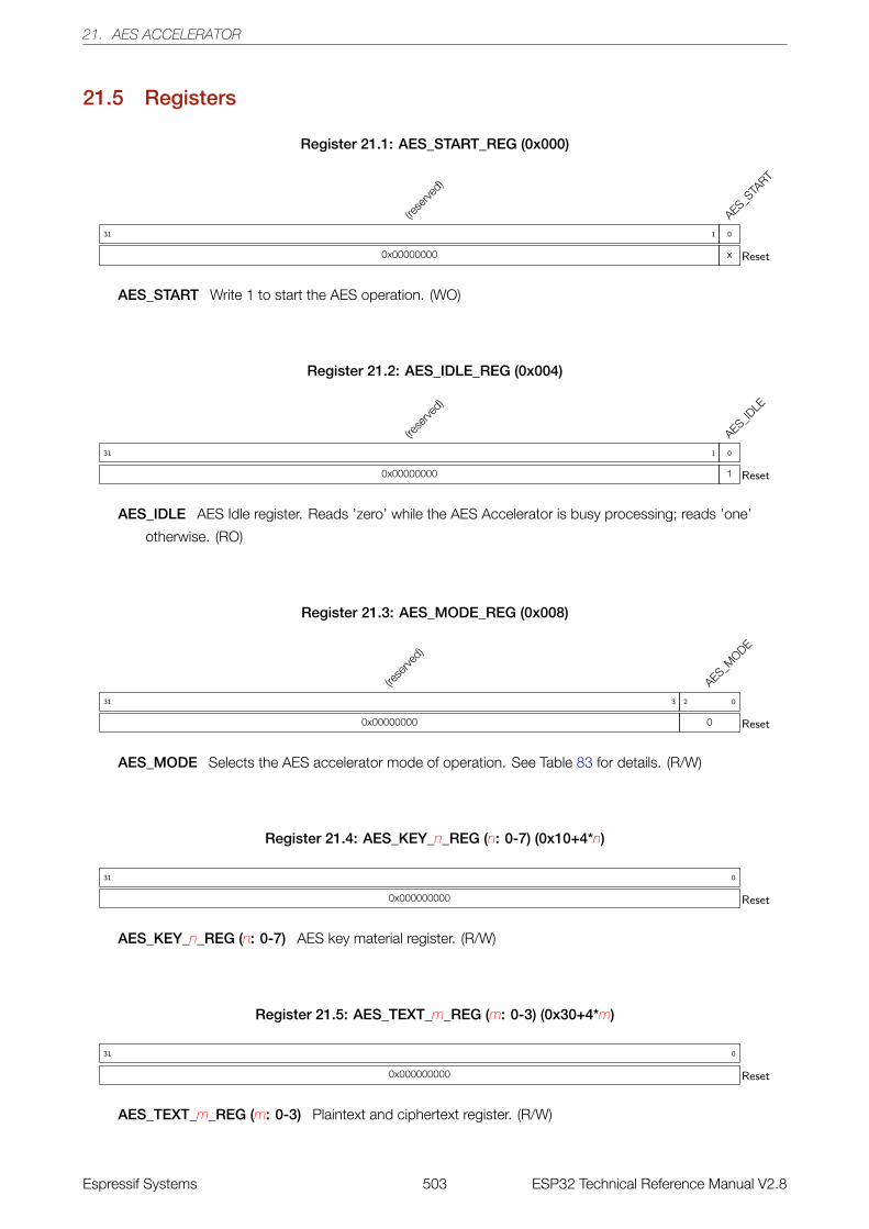
21. AES ACCELERATOR
21.5 Registers
Register 21.1: AES_START_REG (0x000)
(rese
rved)
0x00000000
31 1
AES_STA
RT
x
0
Reset
AES_START Write 1 to start the AES operation. (WO)
Register 21.2: AES_IDLE_REG (0x004)
(rese
rved)
0x00000000
31 1
AES_IDLE
1
0
Reset
AES_IDLE AES Idle register. Reads ’zero’ while the AES Accelerator is busy processing; reads ’one’
otherwise. (RO)
Register 21.3: AES_MODE_REG (0x008)
(rese
rved)
0x00000000
31 3
AES_MODE
0
2 0
Reset
AES_MODE Selects the AES accelerator mode of operation. See Table 83 for details. (R/W)
Register 21.4: AES_KEY_n_REG (n: 0-7) (0x10+4*n)
0x000000000
31 0
Reset
AES_KEY_n_REG (n: 0-7) AES key material register. (R/W)
Register 21.5: AES_TEXT_m_REG (m: 0-3) (0x30+4*m)
0x000000000
31 0
Reset
AES_TEXT_m_REG (m: 0-3) Plaintext and ciphertext register. (R/W)
Espressif Systems 503 ESP32 Technical Reference Manual V2.8
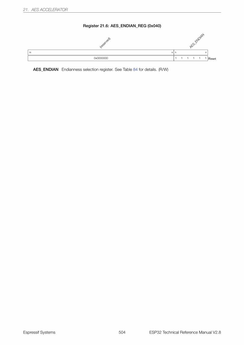
21. AES ACCELERATOR
Register 21.6: AES_ENDIAN_REG (0x040)
(rese
rved)
0x0000000
31 6
AES_ENDIA
N
1 1 1 1 1 1
5 0
Reset
AES_ENDIAN Endianness selection register. See Table 84 for details. (R/W)
Espressif Systems 504 ESP32 Technical Reference Manual V2.8
22. SHA ACCELERATOR
22. SHA Accelerator
22.1 Introduction
The SHA Accelerator is included to speed up SHA hashing operations significantly, compared to SHA hashing
algorithms implemented solely in software. The SHA Accelerator supports four algorithms of FIPS PUB 180-4,
specifically SHA-1, SHA-256, SHA-384 and SHA-512.
22.2 Features
Hardware support for popular secure hashing algorithms:
• SHA-1
• SHA-256
• SHA-384
• SHA-512
22.3 Functional Description
22.3.1 Padding and Parsing the Message
The SHA Accelerator can only accept one message block at a time. Software divides the message into blocks
according to “5.2 Parsing the Message” in FIPS PUB 180-4 and writes one block to the SHA_TEXT_n_REG
registers each time. For SHA-1 and SHA-256, software writes a 512-bit message block to SHA_TEXT_0_REG
~ SHA_TEXT_15_REG each time. For SHA-384 and SHA-512, software writes a 1024-bit message block to
SHA_TEXT_0_REG ~ SHA_TEXT_31_REG each time.
The SHA Accelerator is unable to perform the padding operation of “5.1 Padding the Message” in FIPS PUB
180-4; Note that the user software is expected to pad the message before feeding it into the accelerator.
As described in “2.2.1: Parameters” in FIPS PUB 180-4, “M (i)0 is the leftmost word of message block i”. M (i)
0 is
stored in SHA_TEXT_0_REG. In the same fashion, the SHA_TEXT_1_REG register stores the second left-most
word of a message blockH(N)1 , etc.
22.3.2 Message Digest
When the hashing operation is finished, the message digest will be refreshed by SHA Accelerator and will be
stored in SHA_TEXT_n_REG. SHA-1 produces a 160-bit message digest and stores it in SHA_TEXT_0_REG ~SHA_TEXT_4_REG. SHA-256 produces a 256-bit message digest and stores it in SHA_TEXT_0_REG ~SHA_TEXT_7_REG. SHA-384 produces a 384-bit message digest and stores it in SHA_TEXT_0_REG ~SHA_TEXT_11_REG. SHA-512 produces a 512-bit message digest and stores it in SHA_TEXT_0_REG ~SHA_TEXT_15_REG.
As described in “2.2.1 Parameters” in FIPS PUB 180-4, “H(N) is the final hash value, and is used to determine
the message digest”, while “H(i)0 is the leftmost word of hash value i”, so the leftmost word H
(N)0 in the message
digest is stored in SHA_TEXT_0_REG. In the same fashion, the second leftmost word H(N)1 in the message
digest is stored in SHA_TEXT_1_REG, etc.
Espressif Systems 505 ESP32 Technical Reference Manual V2.8
22. SHA ACCELERATOR
22.3.3 Hash Operation
There is a set of control registers for SHA-1, SHA-256, SHA-384 and SHA-512, respectively; different hashing
algorithms use different control registers.
SHA-1 uses SHA_SHA1_START_REG, SHA_SHA1_CONTINUE_REG, SHA_SHA1_LOAD_REG and
SHA_SHA1_BUSY_REG.
SHA-256 uses SHA_SHA256_START_REG, SHA_SHA256_CONTINUE_REG,
SHA_SHA256_LOAD_REG and SHA_SHA256_BUSY_REG. SHA-384 uses SHA_SHA384_START_REG,
SHA_SHA384_CONTINUE_REG, SHA_SHA384_LOAD_REG and SHA_SHA384_BUSY_REG.
SHA-512 uses SHA_SHA512_START_REG, SHA_SHA512_CONTINUE_REG, SHA_SHA512_LOAD_REG
and SHA_SHA512_BUSY_REG. The following steps describe the operation in a detailed manner.
1. Feed the accelerator with the first message block:
(a) Use the first message block to initialize SHA_TEXT_n_REG.
(b) Write 1 to SHA_X_START_REG.
(c) Wait for SHA_X_BUSY_REG to read 0, indicating that the operation is completed.
2. Similarly, feed the accelerator with subsequent message blocks:
(a) Initialize SHA_TEXT_n_REG using the subsequent message block.
(b) Write 1 to SHA_X_CONTINUE_REG.
(c) Wait for SHA_X_BUSY_REG to read 0, indicating that the operation is completed.
3. Get message digest:
(a) Write 1 to SHA_X_LOAD_REG.
(b) Wait for SHA_X_BUSY_REG to read 0, indicating that operation is completed.
(c) Read message digest from SHA_TEXT_n_REG.
22.3.4 Speed
The SHA Accelerator requires 60 to 100 clock cycles to process a message block and 8 to 20 clock cycles to
calculate the final digest.
22.4 Register Summary
Name Description Address Access
Encrypted/decrypted data registers
SHA_TEXT_0_REG SHA encrypted/decrypted data register 0 0x3FF03000 R/W
SHA_TEXT_1_REG SHA encrypted/decrypted data register 1 0x3FF03004 R/W
SHA_TEXT_2_REG SHA encrypted/decrypted data register 2 0x3FF03008 R/W
SHA_TEXT_3_REG SHA encrypted/decrypted data register 3 0x3FF0300C R/W
SHA_TEXT_4_REG SHA encrypted/decrypted data register 4 0x3FF03010 R/W
SHA_TEXT_5_REG SHA encrypted/decrypted data register 5 0x3FF03014 R/W
SHA_TEXT_6_REG SHA encrypted/decrypted data register 6 0x3FF03018 R/W
SHA_TEXT_7_REG SHA encrypted/decrypted data register 7 0x3FF0301C R/W
Espressif Systems 506 ESP32 Technical Reference Manual V2.8
22. SHA ACCELERATOR
Name Description Address Access
SHA_TEXT_8_REG SHA encrypted/decrypted data register 8 0x3FF03020 R/W
SHA_TEXT_9_REG SHA encrypted/decrypted data register 9 0x3FF03024 R/W
SHA_TEXT_10_REG SHA encrypted/decrypted data register 10 0x3FF03028 R/W
SHA_TEXT_11_REG SHA encrypted/decrypted data register 11 0x3FF0302C R/W
SHA_TEXT_12_REG SHA encrypted/decrypted data register 12 0x3FF03030 R/W
SHA_TEXT_13_REG SHA encrypted/decrypted data register 13 0x3FF03034 R/W
SHA_TEXT_14_REG SHA encrypted/decrypted data register 14 0x3FF03038 R/W
SHA_TEXT_15_REG SHA encrypted/decrypted data register 15 0x3FF0303C R/W
SHA_TEXT_16_REG SHA encrypted/decrypted data register 16 0x3FF03040 R/W
SHA_TEXT_17_REG SHA encrypted/decrypted data register 17 0x3FF03044 R/W
SHA_TEXT_18_REG SHA encrypted/decrypted data register 18 0x3FF03048 R/W
SHA_TEXT_19_REG SHA encrypted/decrypted data register 19 0x3FF0304C R/W
SHA_TEXT_20_REG SHA encrypted/decrypted data register 20 0x3FF03050 R/W
SHA_TEXT_21_REG SHA encrypted/decrypted data register 21 0x3FF03054 R/W
SHA_TEXT_22_REG SHA encrypted/decrypted data register 22 0x3FF03058 R/W
SHA_TEXT_23_REG SHA encrypted/decrypted data register 23 0x3FF0305C R/W
SHA_TEXT_24_REG SHA encrypted/decrypted data register 24 0x3FF03060 R/W
SHA_TEXT_25_REG SHA encrypted/decrypted data register 25 0x3FF03064 R/W
SHA_TEXT_26_REG SHA encrypted/decrypted data register 26 0x3FF03068 R/W
SHA_TEXT_27_REG SHA encrypted/decrypted data register 27 0x3FF0306C R/W
SHA_TEXT_28_REG SHA encrypted/decrypted data register 28 0x3FF03070 R/W
SHA_TEXT_29_REG SHA encrypted/decrypted data register 29 0x3FF03074 R/W
SHA_TEXT_30_REG SHA encrypted/decrypted data register 30 0x3FF03078 R/W
SHA_TEXT_31_REG SHA encrypted/decrypted data register 31 0x3FF0307C R/W
Control/status registers
SHA_SHA1_START_REG Control register to initiate SHA1 operation 0x3FF03080 WO
SHA_SHA1_CONTINUE_REG Control register to continue SHA1 operation 0x3FF03084 WO
SHA_SHA1_LOAD_REG Control register to calculate the final SHA1 hash 0x3FF03088 WO
SHA_SHA1_BUSY_REG Status register for SHA1 operation 0x3FF0308C RO
SHA_SHA256_START_REG Control register to initiate SHA256 operation 0x3FF03090 WO
SHA_SHA256_CONTINUE_REG Control register to continue SHA256 operation 0x3FF03094 WO
SHA_SHA256_LOAD_REGControl register to calculate the final SHA256
hash0x3FF03098 WO
SHA_SHA256_BUSY_REG Status register for SHA256 operation 0x3FF0309C RO
SHA_SHA384_START_REG Control register to initiate SHA384 operation 0x3FF030A0 WO
SHA_SHA384_CONTINUE_REG Control register to continue SHA384 operation 0x3FF030A4 WO
SHA_SHA384_LOAD_REGControl register to calculate the final SHA384
hash0x3FF030A8 WO
SHA_SHA384_BUSY_REG Status register for SHA384 operation 0x3FF030AC RO
SHA_SHA512_START_REG Control register to initiate SHA512 operation 0x3FF030B0 WO
SHA_SHA512_CONTINUE_REG Control register to continue SHA512 operation 0x3FF030B4 WO
SHA_SHA512_LOAD_REGControl register to calculate the final SHA512
hash0x3FF030B8 WO
SHA_SHA512_BUSY_REG Status register for SHA512 operation 0x3FF030BC RO
Espressif Systems 507 ESP32 Technical Reference Manual V2.8
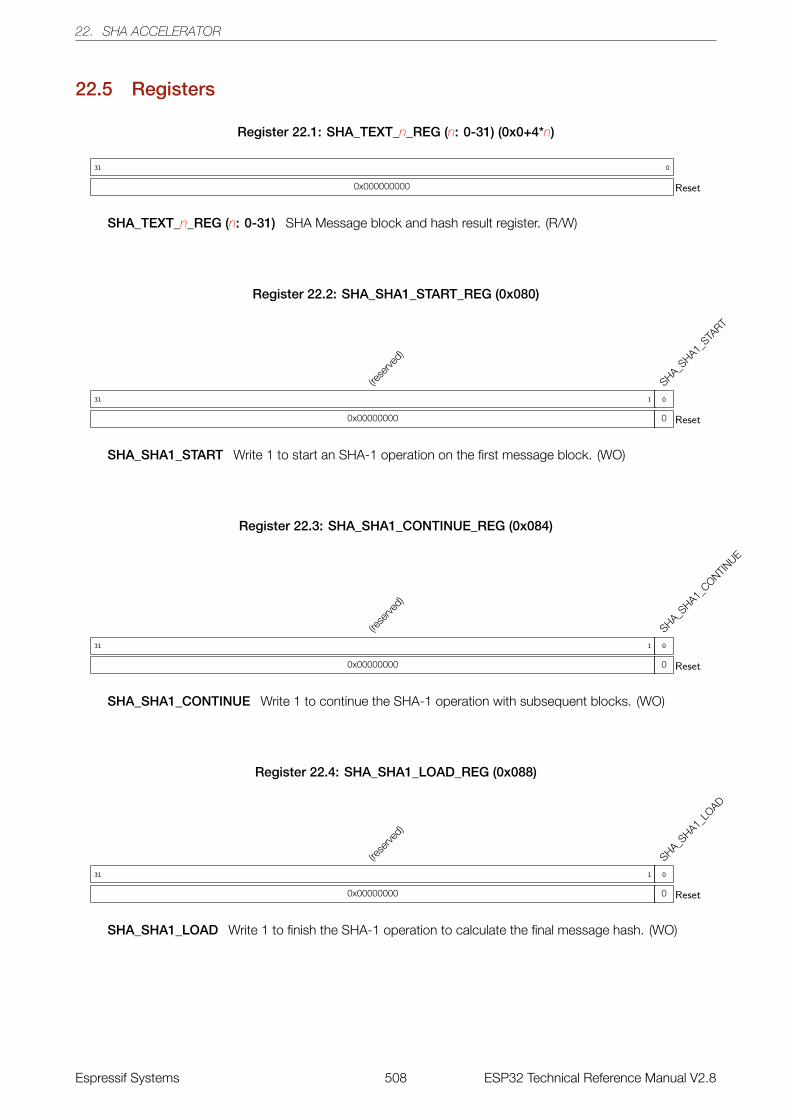
22. SHA ACCELERATOR
22.5 Registers
Register 22.1: SHA_TEXT_n_REG (n: 0-31) (0x0+4*n)
0x000000000
31 0
Reset
SHA_TEXT_n_REG (n: 0-31) SHA Message block and hash result register. (R/W)
Register 22.2: SHA_SHA1_START_REG (0x080)
(rese
rved)
0x00000000
31 1
SHA_SHA1_
START
0
0
Reset
SHA_SHA1_START Write 1 to start an SHA-1 operation on the first message block. (WO)
Register 22.3: SHA_SHA1_CONTINUE_REG (0x084)
(rese
rved)
0x00000000
31 1
SHA_SHA1_
CONTINUE
0
0
Reset
SHA_SHA1_CONTINUE Write 1 to continue the SHA-1 operation with subsequent blocks. (WO)
Register 22.4: SHA_SHA1_LOAD_REG (0x088)
(rese
rved)
0x00000000
31 1
SHA_SHA1_
LOAD
0
0
Reset
SHA_SHA1_LOAD Write 1 to finish the SHA-1 operation to calculate the final message hash. (WO)
Espressif Systems 508 ESP32 Technical Reference Manual V2.8

22. SHA ACCELERATOR
Register 22.5: SHA_SHA1_BUSY_REG (0x08C)
(rese
rved)
0x00000000
31 1
SHA_SHA1_
BUSY
0
0
Reset
SHA_SHA1_BUSY SHA-1 operation status: 1 if the SHA accelerator is processing data, 0 if it is idle.
(RO)
Register 22.6: SHA_SHA256_START_REG (0x090)
(rese
rved)
0x00000000
31 1
SHA_SHA25
6_STA
RT
0
0
Reset
SHA_SHA256_START Write 1 to start an SHA-256 operation on the first message block. (WO)
Register 22.7: SHA_SHA256_CONTINUE_REG (0x094)
(rese
rved)
0x00000000
31 1
SHA_SHA25
6_CONTIN
UE
0
0
Reset
SHA_SHA256_CONTINUE Write 1 to continue the SHA-256 operation with subsequent blocks. (WO)
Register 22.8: SHA_SHA256_LOAD_REG (0x098)
(rese
rved)
0x00000000
31 1
SHA_SHA25
6_LO
AD
0
0
Reset
SHA_SHA256_LOAD Write 1 to finish the SHA-256 operation to calculate the final message hash.
(WO)
Espressif Systems 509 ESP32 Technical Reference Manual V2.8

22. SHA ACCELERATOR
Register 22.9: SHA_SHA256_BUSY_REG (0x09C)
(rese
rved)
0x00000000
31 1
SHA_SHA25
6_BUSY
0
0
Reset
SHA_SHA256_BUSY SHA-256 operation status: 1 if the SHA accelerator is processing data, 0 if it
is idle. (RO)
Register 22.10: SHA_SHA384_START_REG (0x0A0)
(rese
rved)
0x00000000
31 1
SHA_SHA38
4_STA
RT
0
0
Reset
SHA_SHA384_START Write 1 to start an SHA-384 operation on the first message block. (WO)
Register 22.11: SHA_SHA384_CONTINUE_REG (0x0A4)
(rese
rved)
0x00000000
31 1
SHA_SHA38
4_CONTIN
UE
0
0
Reset
SHA_SHA384_CONTINUE Write 1 to continue the SHA-384 operation with subsequent blocks. (WO)
Register 22.12: SHA_SHA384_LOAD_REG (0x0A8)
(rese
rved)
0x00000000
31 1
SHA_SHA38
4_LO
AD
0
0
Reset
SHA_SHA384_LOAD Write 1 to finish the SHA-384 operation to calculate the final message hash.
(WO)
Espressif Systems 510 ESP32 Technical Reference Manual V2.8
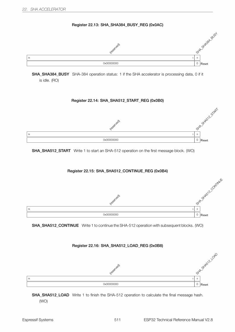
22. SHA ACCELERATOR
Register 22.13: SHA_SHA384_BUSY_REG (0x0AC)
(rese
rved)
0x00000000
31 1
SHA_SHA38
4_BUSY
0
0
Reset
SHA_SHA384_BUSY SHA-384 operation status: 1 if the SHA accelerator is processing data, 0 if it
is idle. (RO)
Register 22.14: SHA_SHA512_START_REG (0x0B0)
(rese
rved)
0x00000000
31 1
SHA_SHA51
2_STA
RT
0
0
Reset
SHA_SHA512_START Write 1 to start an SHA-512 operation on the first message block. (WO)
Register 22.15: SHA_SHA512_CONTINUE_REG (0x0B4)
(rese
rved)
0x00000000
31 1
SHA_SHA51
2_CONTIN
UE
0
0
Reset
SHA_SHA512_CONTINUE Write 1 to continue the SHA-512 operation with subsequent blocks. (WO)
Register 22.16: SHA_SHA512_LOAD_REG (0x0B8)
(rese
rved)
0x00000000
31 1
SHA_SHA51
2_LO
AD
0
0
Reset
SHA_SHA512_LOAD Write 1 to finish the SHA-512 operation to calculate the final message hash.
(WO)
Espressif Systems 511 ESP32 Technical Reference Manual V2.8
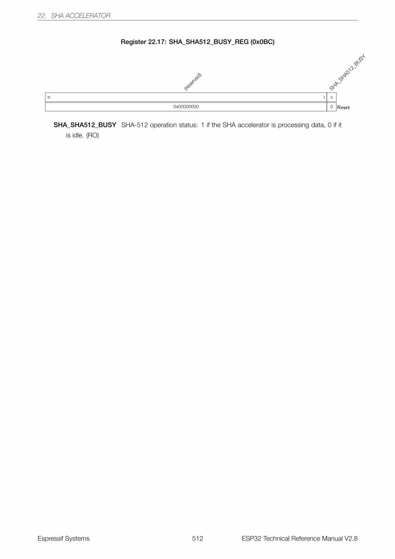
22. SHA ACCELERATOR
Register 22.17: SHA_SHA512_BUSY_REG (0x0BC)
(rese
rved)
0x00000000
31 1
SHA_SHA51
2_BUSY
0
0
Reset
SHA_SHA512_BUSY SHA-512 operation status: 1 if the SHA accelerator is processing data, 0 if it
is idle. (RO)
Espressif Systems 512 ESP32 Technical Reference Manual V2.8
23. RSA ACCELERATOR
23. RSA Accelerator
23.1 Introduction
The RSA Accelerator provides hardware support for multiple precision arithmetic operations used in RSA
asymmetric cipher algorithms.
Sometimes, multiple precision arithmetic is also called ”bignum arithmetic”, ”bigint arithmetic” or ”arbitrary
precision arithmetic”.
23.2 Features
• Support for large-number modular exponentiation
• Support for large-number modular multiplication
• Support for large-number multiplication
• Support for various lengths of operands
23.3 Functional Description
23.3.1 Initialization
The RSA Accelerator is activated by enabling the corresponding peripheral clock, and by clearing the
DPORT_RSA_PD bit in the DPORT_RSA_PD_CTRL_REG register. This releases the RSA Accelerator from
reset.
When the RSA Accelerator is released from reset, the register RSA_CLEAN_REG reads 0 and an initialization
process begins. Hardware initializes the four memory blocks by setting them to 0. After initialization is complete,
RSA_CLEAN_REG reads 1. For this reason, software should query RSA_CLEAN_REG after being released from
reset, and before writing to any RSA Accelerator memory blocks or registers for the first time.
23.3.2 Large Number Modular Exponentiation
Large-number modular exponentiation performs Z = XY mod M . The operation is based on Montgomery
multiplication. Aside from the arguments X, Y , and M , two additional ones are needed — r and M ′. These
arguments are calculated in advance by software.
The RSA Accelerator supports operand lengths of N ∈ {512, 1024, 1536, 2048, 2560, 3072, 3584, 4096} bits. The
bit length of arguments Z, X, Y , M , and r can be any one from the N set, but all numbers in a calculation must
be of the same length. The bit length of M ′ is always 32.
To represent the numbers used as operands, define a base-b positional notation, as follows:
b = 232
Espressif Systems 513 ESP32 Technical Reference Manual V2.8
23. RSA ACCELERATOR
In this notation, each number is represented by a sequence of base-b digits, where each base-b digit is a 32-bit
word. Representing an N-bit number requires n base-b digits (all of the possible N lengths are multiples of
32).
n =N
32
Z = (Zn−1Zn−2 · · ·Z0)b
X = (Xn−1Xn−2 · · ·X0)b
Y = (Yn−1Yn−2 · · ·Y0)b
M = (Mn−1Mn−2 · · ·M0)b
r = (rn−1rn−2 · · · r0)b
Each of the n values in Zn−1 ~ Z0, Xn−1 ~ X0, Yn−1 ~ Y0, Mn−1 ~ M0, rn−1 ~ r0 represents one base-b digit (a
32-bit word).
Zn−1, Xn−1, Yn−1, Mn−1 and rn−1 are the most significant bits of Z, X, Y , M , while Z0, X0, Y0, M0 and r0 are
the least significant bits.
If we define
R = bn
then, we can calculate the additional arguments, as follows:
r = R2 mod M (1)M ′′ ×M + 1 = R×R−1
M ′ = M ′′ mod b(2)
(Equation 2 is written in a form suitable for calculations using the extended binary GCD algorithm.)
Software can implement large-number modular exponentiations in the following order:
1. Write ( N512 − 1) to RSA_MODEXP_MODE_REG.
2. Write Xi, Yi, Mi and ri (i ∈ [0, n) ∩ N) to memory blocks RSA_X_MEM, RSA_Y_MEM, RSA_M_MEM and
RSA_Z_MEM. The capacity of each memory block is 128 words. Each word of each memory block can
store one base-b digit. The memory blocks use the little endian format for storage, i.e. the least significant
digit of each number is in the lowest address.
Users need to write data to each memory block only according to the length of the number; data beyond
this length are ignored.
3. Write M ′ to RSA_M_PRIME_REG.
4. Write 1 to RSA_MODEXP_START_REG.
5. Wait for the operation to be completed. Poll RSA_INTERRUPT_REG until it reads 1, or until the RSA_INTR
interrupt is generated.
6. Read the result Zi (i ∈ [0, n) ∩ N) from RSA_Z_MEM.
7. Write 1 to RSA_INTERRUPT_REG to clear the interrupt.
After the operation, the RSA_MODEXP_MODE_REG register, memory blocks RSA_Y_MEM and RSA_M_MEM,
as well as the RSA_M_PRIME_REG will not have changed. However, Xi in RSA_X_MEM and ri in RSA_Z_MEM
Espressif Systems 514 ESP32 Technical Reference Manual V2.8
23. RSA ACCELERATOR
will have been overwritten. In order to perform another operation, refresh the registers and memory blocks, as
required.
23.3.3 Large Number Modular Multiplication
Large-number modular multiplication performs Z = X × Y mod M . This operation is based on Montgomery
multiplication. The same values r and M ′ are derived by software using the formulas 1 and 2 shown
above.
The RSA Accelerator supports large-number modular multiplication with eight different operand lengths, which
are the same as in the large-number modular exponentiation. The operation is performed by a combination of
software and hardware. The software performs two hardware operations in sequence.
The software process is as follows:
1. Write ( N512 − 1) to RSA_MULT_MODE_REG.
2. Write Xi, Mi and ri (i ∈ [0, n) ∩ N) to registers RSA_X_MEM, RSA_M_MEM and RSA_Z_MEM. Write data
to each memory block only according to the length of the number. Data beyond this length are ignored.
3. Write M ′ to RSA_M_PRIME_REG.
4. Write 1 to RSA_MULT_START_REG.
5. Wait for the first round of the operation to be completed. Poll RSA_INTERRUPT_REG until it reads 1, or
until the RSA_INTR interrupt is generated.
6. Write 1 to RSA_INTERRUPT_REG to clear the interrupt.
7. Write Yi (i ∈ [0, n) ∩ N) to RSA_X_MEM.
Users need to write to the memory block only according to the length of the number. Data beyond this
length are ignored.
8. Write 1 to RSA_MULT_START_REG.
9. Wait for the second round of the operation to be completed. Poll RSA_INTERRUPT_REG until it reads 1, or
until the RSA_INTR interrupt is generated.
10. Read the result Zi (i ∈ [0, n) ∩ N) from RSA_Z_MEM.
11. Write 1 to RSA_INTERRUPT_REG to clear the interrupt.
After the operation, the RSA_MULT_MODE_REG register, and memory blocks RSA_M_MEM and
RSA_M_PRIME_REG remain unchanged. Users do not need to refresh these registers or memory blocks if the
values remain the same.
23.3.4 Large Number Multiplication
Large-number multiplication performs Z = X × Y . The length of Z is twice that of X and Y . Therefore, the RSA
Accelerator supports large-number multiplication with only four operand lengths of N ∈ {512, 1024, 1536, 2048}bits. The length N of the result Z is 2×N bits.
Operands X and Y need to be extended to form arguments X and Y which have the same length (N bits) as
Espressif Systems 515 ESP32 Technical Reference Manual V2.8
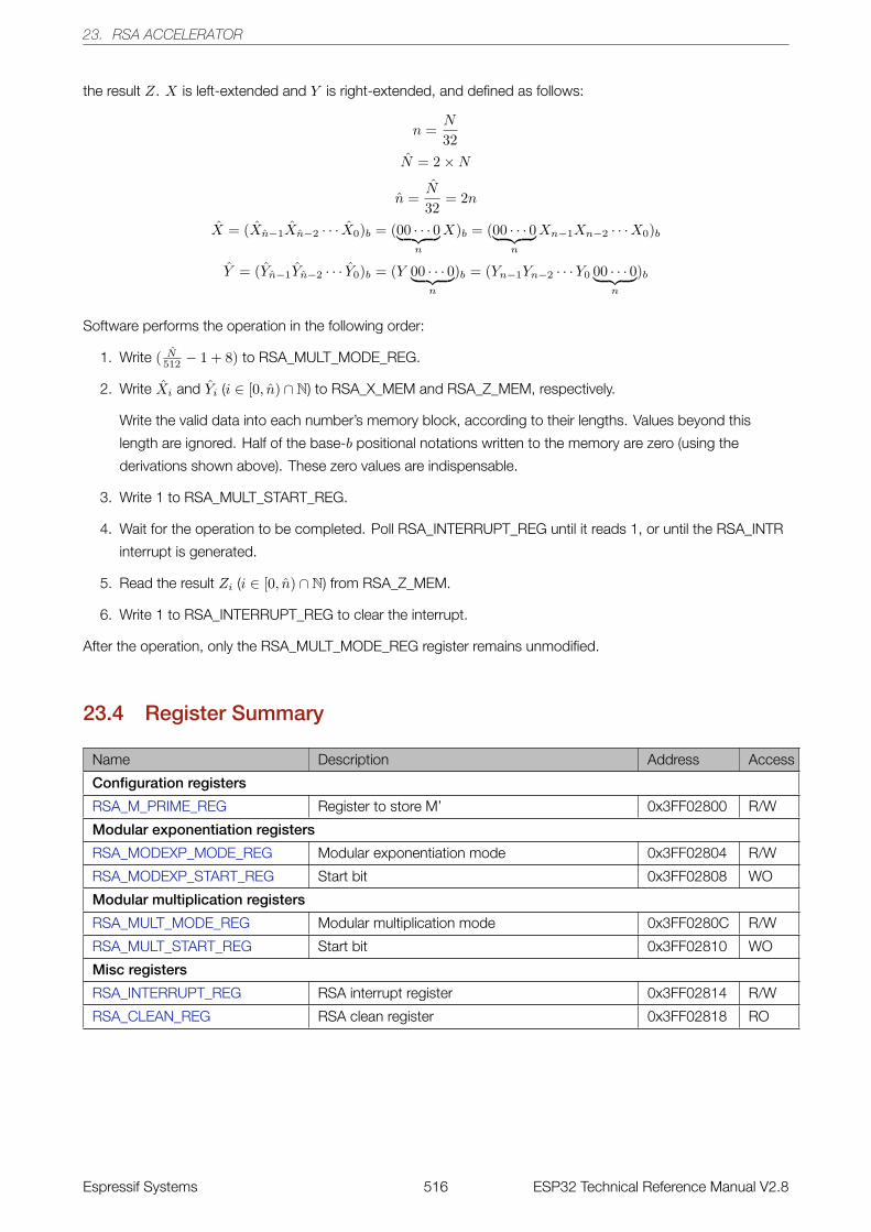
23. RSA ACCELERATOR
the result Z. X is left-extended and Y is right-extended, and defined as follows:
n =N
32
N = 2×N
n =N
32= 2n
X = (Xn−1Xn−2 · · · X0)b = (00 · · · 0︸ ︷︷ ︸n
X)b = (00 · · · 0︸ ︷︷ ︸n
Xn−1Xn−2 · · ·X0)b
Y = (Yn−1Yn−2 · · · Y0)b = (Y 00 · · · 0︸ ︷︷ ︸n
)b = (Yn−1Yn−2 · · ·Y0 00 · · · 0︸ ︷︷ ︸n
)b
Software performs the operation in the following order:
1. Write ( N512 − 1 + 8) to RSA_MULT_MODE_REG.
2. Write Xi and Yi (i ∈ [0, n) ∩ N) to RSA_X_MEM and RSA_Z_MEM, respectively.
Write the valid data into each number’s memory block, according to their lengths. Values beyond this
length are ignored. Half of the base-b positional notations written to the memory are zero (using the
derivations shown above). These zero values are indispensable.
3. Write 1 to RSA_MULT_START_REG.
4. Wait for the operation to be completed. Poll RSA_INTERRUPT_REG until it reads 1, or until the RSA_INTR
interrupt is generated.
5. Read the result Zi (i ∈ [0, n) ∩ N) from RSA_Z_MEM.
6. Write 1 to RSA_INTERRUPT_REG to clear the interrupt.
After the operation, only the RSA_MULT_MODE_REG register remains unmodified.
23.4 Register Summary
Name Description Address Access
Configuration registers
RSA_M_PRIME_REG Register to store M’ 0x3FF02800 R/W
Modular exponentiation registers
RSA_MODEXP_MODE_REG Modular exponentiation mode 0x3FF02804 R/W
RSA_MODEXP_START_REG Start bit 0x3FF02808 WO
Modular multiplication registers
RSA_MULT_MODE_REG Modular multiplication mode 0x3FF0280C R/W
RSA_MULT_START_REG Start bit 0x3FF02810 WO
Misc registers
RSA_INTERRUPT_REG RSA interrupt register 0x3FF02814 R/W
RSA_CLEAN_REG RSA clean register 0x3FF02818 RO
Espressif Systems 516 ESP32 Technical Reference Manual V2.8
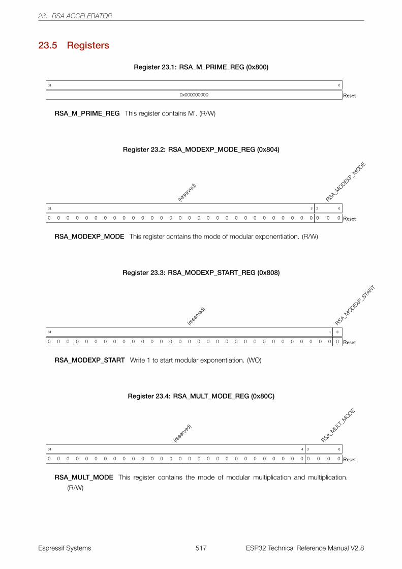
23. RSA ACCELERATOR
23.5 Registers
Register 23.1: RSA_M_PRIME_REG (0x800)
0x000000000
31 0
Reset
RSA_M_PRIME_REG This register contains M’. (R/W)
Register 23.2: RSA_MODEXP_MODE_REG (0x804)
(rese
rved)
0 0 0 0 0 0 0 0 0 0 0 0 0 0 0 0 0 0 0 0 0 0 0 0 0 0 0 0 0
31 3
RSA_MODEXP
_MODE
0 0 0
2 0
Reset
RSA_MODEXP_MODE This register contains the mode of modular exponentiation. (R/W)
Register 23.3: RSA_MODEXP_START_REG (0x808)
(rese
rved)
0 0 0 0 0 0 0 0 0 0 0 0 0 0 0 0 0 0 0 0 0 0 0 0 0 0 0 0 0 0 0
31 1
RSA_MODEXP
_STA
RT
0
0
Reset
RSA_MODEXP_START Write 1 to start modular exponentiation. (WO)
Register 23.4: RSA_MULT_MODE_REG (0x80C)
(rese
rved)
0 0 0 0 0 0 0 0 0 0 0 0 0 0 0 0 0 0 0 0 0 0 0 0 0 0 0 0
31 4
RSA_MULT
_MODE
0 0 0 0
3 0
Reset
RSA_MULT_MODE This register contains the mode of modular multiplication and multiplication.
(R/W)
Espressif Systems 517 ESP32 Technical Reference Manual V2.8
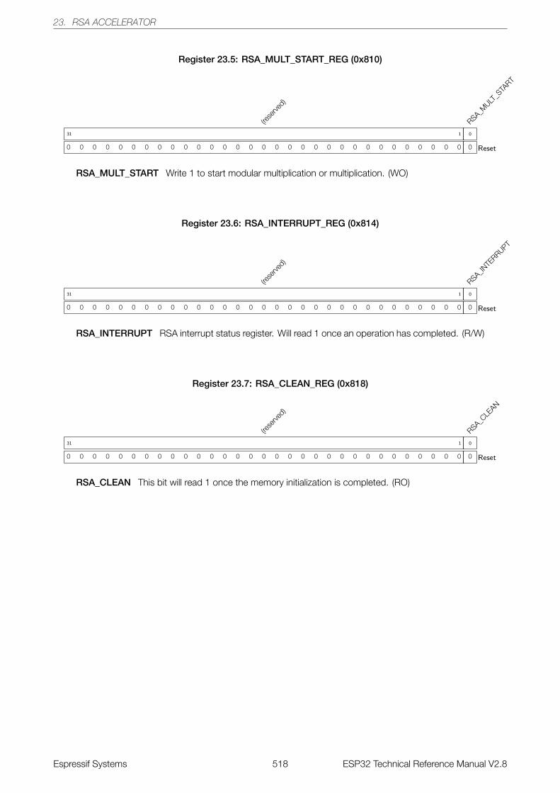
23. RSA ACCELERATOR
Register 23.5: RSA_MULT_START_REG (0x810)
(rese
rved)
0 0 0 0 0 0 0 0 0 0 0 0 0 0 0 0 0 0 0 0 0 0 0 0 0 0 0 0 0 0 0
31 1
RSA_MULT
_STA
RT
0
0
Reset
RSA_MULT_START Write 1 to start modular multiplication or multiplication. (WO)
Register 23.6: RSA_INTERRUPT_REG (0x814)
(rese
rved)
0 0 0 0 0 0 0 0 0 0 0 0 0 0 0 0 0 0 0 0 0 0 0 0 0 0 0 0 0 0 0
31 1
RSA_INTE
RRUPT
0
0
Reset
RSA_INTERRUPT RSA interrupt status register. Will read 1 once an operation has completed. (R/W)
Register 23.7: RSA_CLEAN_REG (0x818)
(rese
rved)
0 0 0 0 0 0 0 0 0 0 0 0 0 0 0 0 0 0 0 0 0 0 0 0 0 0 0 0 0 0 0
31 1
RSA_CLE
AN
0
0
Reset
RSA_CLEAN This bit will read 1 once the memory initialization is completed. (RO)
Espressif Systems 518 ESP32 Technical Reference Manual V2.8
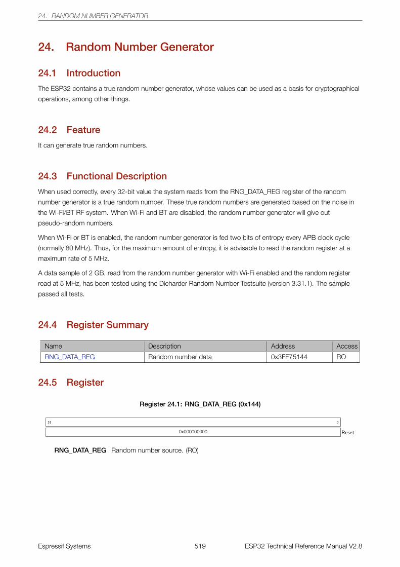
24. RANDOM NUMBER GENERATOR
24. Random Number Generator
24.1 Introduction
The ESP32 contains a true random number generator, whose values can be used as a basis for cryptographical
operations, among other things.
24.2 Feature
It can generate true random numbers.
24.3 Functional Description
When used correctly, every 32-bit value the system reads from the RNG_DATA_REG register of the random
number generator is a true random number. These true random numbers are generated based on the noise in
the Wi-Fi/BT RF system. When Wi-Fi and BT are disabled, the random number generator will give out
pseudo-random numbers.
When Wi-Fi or BT is enabled, the random number generator is fed two bits of entropy every APB clock cycle
(normally 80 MHz). Thus, for the maximum amount of entropy, it is advisable to read the random register at a
maximum rate of 5 MHz.
A data sample of 2 GB, read from the random number generator with Wi-Fi enabled and the random register
read at 5 MHz, has been tested using the Dieharder Random Number Testsuite (version 3.31.1). The sample
passed all tests.
24.4 Register Summary
Name Description Address Access
RNG_DATA_REG Random number data 0x3FF75144 RO
24.5 Register
Register 24.1: RNG_DATA_REG (0x144)
0x000000000
31 0
Reset
RNG_DATA_REG Random number source. (RO)
Espressif Systems 519 ESP32 Technical Reference Manual V2.8
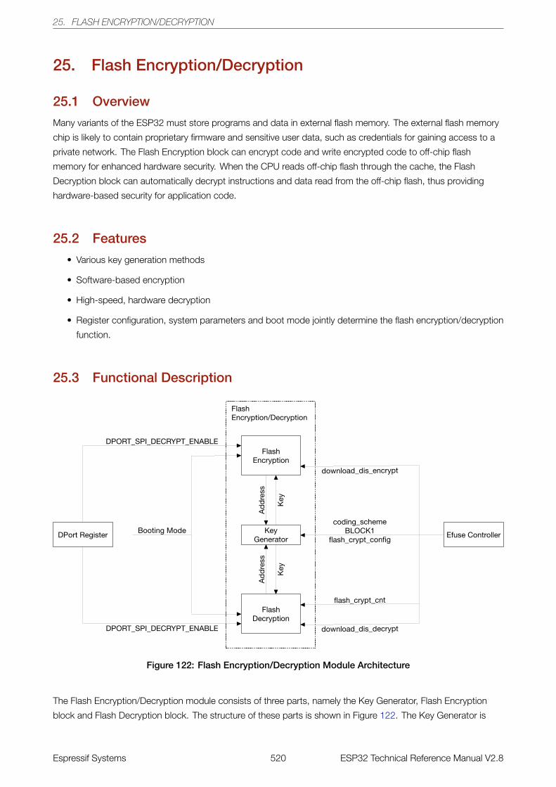
25. FLASH ENCRYPTION/DECRYPTION
25. Flash Encryption/Decryption
25.1 Overview
Many variants of the ESP32 must store programs and data in external flash memory. The external flash memory
chip is likely to contain proprietary firmware and sensitive user data, such as credentials for gaining access to a
private network. The Flash Encryption block can encrypt code and write encrypted code to off-chip flash
memory for enhanced hardware security. When the CPU reads off-chip flash through the cache, the Flash
Decryption block can automatically decrypt instructions and data read from the off-chip flash, thus providing
hardware-based security for application code.
25.2 Features
• Various key generation methods
• Software-based encryption
• High-speed, hardware decryption
• Register configuration, system parameters and boot mode jointly determine the flash encryption/decryption
function.
25.3 Functional Description
Figure 122: Flash Encryption/Decryption Module Architecture
The Flash Encryption/Decryption module consists of three parts, namely the Key Generator, Flash Encryption
block and Flash Decryption block. The structure of these parts is shown in Figure 122. The Key Generator is
Espressif Systems 520 ESP32 Technical Reference Manual V2.8
25. FLASH ENCRYPTION/DECRYPTION
shared by both the Flash Encryption block and the Flash Decryption block, which can function
simultaneously.
In the peripheral DPort Register, the register relevant to Flash Encryption/Decryption is
DPORT_SPI_ENCRYPT_ENABLE bit and DPORT_SPI_DECRYPT_ENABLE bit in
DPORT_SLAVE_SPI_CONFIG_REG. The Flash Encryption/Decryption module will fetch six system parameters
from the peripheral eFuse Controller. These parameters are: coding_scheme, BLOCK1, flash_crypt_config,
download_dis_encrypt, flash_crypt_cnt, and download_dis_decrypt.
25.3.1 Key Generator
According to system parameters coding_scheme and BLOCK1, the Key Generator will first generate
Keyo = f(coding_scheme,BLOCK1).
Then, according to system parameter flash_crypt_config, and off-chip flash physical addresses Addre and Addrd
accessed by the Flash Encryption block and the Flash Decryption block, the Key Generator will respectively figure
out that:
Keye = g(Keyo, f lash_crypt_config,Addre),
Keyd = g(Keyo, f lash_crypt_config,Addrd).
When all values of system parameter flash_crypt_config are 0, Keye and Keyd are not relevant to the physical
address of the off-chip flash. When all values of system parameter flash_crypt_config are not 0, every 8-word
block on the off-chip flash has a dedicated Keye and Keyd.
25.3.2 Flash Encryption Block
The Flash Encryption block is equipped with registers that can be accessed by the CPU directly. Registers
embedded in the Flash Encryption block, registers in the peripheral DPort Register, system parameters and Boot
Mode jointly configure and control this block.
The Flash Encryption block requires software intervention during operation. The steps are as follows:
1. Set the DPORT_SPI_ENCRYPT_ENABLE bit of register DPORT_SLAVE_SPI_CONFIG_REG.
2. Write the physical address prepared for the off-chip flash on register FLASH_ENCRYPT_ADDRESS_REG.
The address must be 8-word boundary aligned.
3. The Flash Encryption block must encrypt 8-word long code segments. Write the lowest word to register
FLASH_ENCRYPT_BUFFER_0_REG, the second-lowest word into FLASH_ENCRYPT_BUFFER_1_REG,
and so on, up to FLASH_ENCRYPT_BUFFER_7_REG.
4. Set the FLASH_START bit in FLASH_ENCRYPT_START_REG.
5. Wait for the FLASH_DONE bit to be set in FLASH_ENCRYPT_DONE_REG.
6. Use this function and write any 8-word code to the 8-word aligned address on the off-chip flash via the
peripheral SPI0.
In Steps 1 to 5, the Flash Encryption block encrypts 8-word long codes. The key encryption algorithm uses
Keye. The encryption result will also be 8-word long. In Step 6, the peripheral SPI0 writes encrypted results of
the Flash Encryption block to the off-chip flash. One parameter of the function used in Step 6 will be the physical
address of the off-chip flash. The physical address must be 8-word boundary aligned. Also, the value must be
the same as the value written into register FLASH_ENCRYPT_ADDRESS_REG during Step 2. Even though the
function used in Step 6 still has a parameter with an 8-word long code, the parameter will be meaningless if
Espressif Systems 521 ESP32 Technical Reference Manual V2.8
25. FLASH ENCRYPTION/DECRYPTION
Steps 1 to 5 are executed. The Peripheral SPI0 will use the encrypted result instead. If the Flash Encryption
block is not operating, or has not executed Steps 1 to 5, Step 6 will not use the encrypted result. Instead, the
function parameter will be used.
Flash Encryption Operating Conditions:
• During SPI Flash Boot
If the DPORT_SPI_ENCRYPT_ENABLE bit of register DPORT_SLAVE_SPI_CONFIG_REG is 1, the Flash
Encryption block is operational. Otherwise, it is not.
• During Download Boot
If the DPORT_SPI_ENCRYPT_ENABLE bit of register DPORT_SLAVE_SPI_CONFIG_REG is 1, and system
parameter download_dis_encrypt is 0, the Flash Encryption block is operational. Otherwise, it is not.
Even though software participates in the whole process, it cannot directly read the encrypted codes. Instead, the
encrypted codes are integrated into the off-chip flash. Even though the CPU can skip the cache and get the
encrypted code directly by reading the off-chip flash, the software can by no means access Keye.
25.3.3 Flash Decryption Block
Flash Decryption is not a conventional peripheral, and is not equipped with registers. Therefore, the CPU cannot
directly access the Flash Decryption block. The Peripheral DPort Register, system parameters and Booting Mode
jointly control and configure the Flash Decryption block.
When the Flash Decryption block is operating, the CPU will read instructions and data from the off-chip flash via
the cache. The Flash Decryption block automatically decrypts the instructions and data in the cache. The entire
decryption process does not need software intervention and is transparent to the cache. The decryption
algorithm can decrypt the code that has been encrypted by the Flash Encryption block. Software cannot access
the key algorithm Keyd used.
When the Flash Encryption block is not operating, it does not have any effect on the contents stored in the
off-chip flash, be they encrypted or unencrypted. What the CPU reads via the cache is the original information
stored in the off-chip flash.
Flash Encryption Operating Conditions:
• During SPI Flash Boot
In the low 7 bits of flash_crypt_cnt, if the number of value 1 is odd, the Flash Decryption block is
operational. Otherwise, it is not.
• During Download Boot
If the DPORT_SPI_DECRYPT_ENABLE bit in DPORT_SLAVE_SPI_CONFIG_REG is 1, and system
parameter download_dis_decrypt is 0, the Flash Decryption block is operational. Otherwise, it is not.
25.4 Register Summary
Name Description Address Access
FLASH_ENCRYPTION_BUFFER_0_REG Flash encryption buffer register 0 0x3FF5B000 WO
FLASH_ENCRYPTION_BUFFER_1_REG Flash encryption buffer register 1 0x3FF5B004 WO
FLASH_ENCRYPTION_BUFFER_2_REG Flash encryption buffer register 2 0x3FF5B008 WO
Espressif Systems 522 ESP32 Technical Reference Manual V2.8
25. FLASH ENCRYPTION/DECRYPTION
Name Description Address Access
FLASH_ENCRYPTION_BUFFER_3_REG Flash encryption buffer register 3 0x3FF5B00C WO
FLASH_ENCRYPTION_BUFFER_4_REG Flash encryption buffer register 4 0x3FF5B010 WO
FLASH_ENCRYPTION_BUFFER_5_REG Flash encryption buffer register 5 0x3FF5B014 WO
FLASH_ENCRYPTION_BUFFER_6_REG Flash encryption buffer register 6 0x3FF5B018 WO
FLASH_ENCRYPTION_BUFFER_7_REG Flash encryption buffer register 7 0x3FF5B01C WO
FLASH_ENCRYPTION_START_REG Encrypt operation control register 0x3FF5B020 WO
FLASH_ENCRYPTION_ADDRESS_REG External flash address register 0x3FF5B024 WO
FLASH_ENCRYPTION_DONE_REG Encrypt operation status register 0x3FF5B028 RO
Espressif Systems 523 ESP32 Technical Reference Manual V2.8
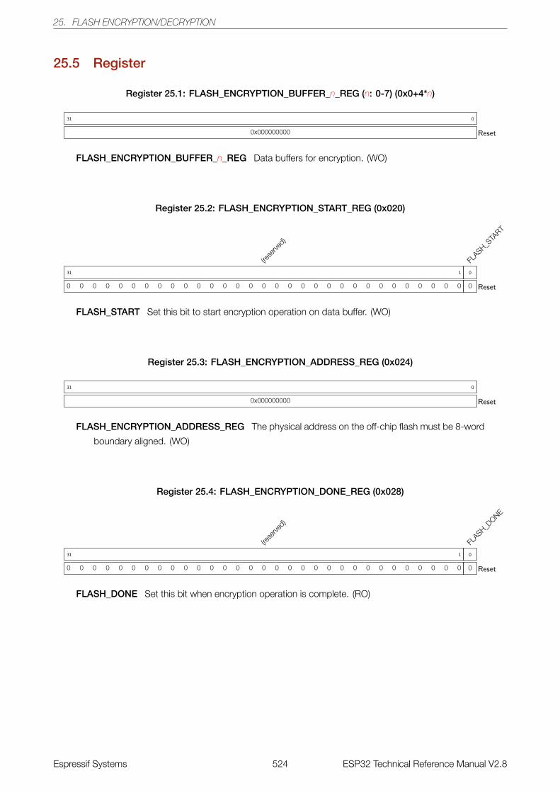
25. FLASH ENCRYPTION/DECRYPTION
25.5 Register
Register 25.1: FLASH_ENCRYPTION_BUFFER_n_REG (n: 0-7) (0x0+4*n)
0x000000000
31 0
Reset
FLASH_ENCRYPTION_BUFFER_n_REG Data buffers for encryption. (WO)
Register 25.2: FLASH_ENCRYPTION_START_REG (0x020)
(rese
rved)
0 0 0 0 0 0 0 0 0 0 0 0 0 0 0 0 0 0 0 0 0 0 0 0 0 0 0 0 0 0 0
31 1
FLASH_S
TART
0
0
Reset
FLASH_START Set this bit to start encryption operation on data buffer. (WO)
Register 25.3: FLASH_ENCRYPTION_ADDRESS_REG (0x024)
0x000000000
31 0
Reset
FLASH_ENCRYPTION_ADDRESS_REG The physical address on the off-chip flash must be 8-word
boundary aligned. (WO)
Register 25.4: FLASH_ENCRYPTION_DONE_REG (0x028)
(rese
rved)
0 0 0 0 0 0 0 0 0 0 0 0 0 0 0 0 0 0 0 0 0 0 0 0 0 0 0 0 0 0 0
31 1
FLASH_D
ONE
0
0
Reset
FLASH_DONE Set this bit when encryption operation is complete. (RO)
Espressif Systems 524 ESP32 Technical Reference Manual V2.8
26. PID/MPU/MMU
26. PID/MPU/MMU
26.1 Introduction
Every peripheral and memory section in the ESP32 is accessed through either an MMU (Memory Management
Unit) or an MPU (Memory Protection Unit). An MPU can allow or disallow the access of an application to a
memory range or peripheral, depending on what kind of permission the OS has given to that particular
application. An MMU can perform the same operation, as well as a virtual-to-physical memory address
translation. This can be used to map an internal or external memory range to a certain virtual memory area.
These mappings can be application-specific. Therefore, each application can be adjusted and have the memory
configuration that is necessary for it to run properly. To differentiate between the OS and applications, there are
eight Process Identifiers (or PIDs) that each application, or OS, can run. Furthermore, each application, or OS, is
equipped with their own sets of mappings and rights.
26.2 Features
• Eight processes in each of the PRO_CPU and APP_CPU
• MPU/MMU management of on-chip memories, off-chip memories, and peripherals, based on process ID
• On-chip memory management by MPU/MMU
• Off-chip memory management by MMU
• Peripheral management by MPU
26.3 Functional Description
26.3.1 PID Controller
In the ESP32, a PID controller acts as an indicator that signals the MMU/MPU the owner PID of the code that is
currently running. The intention is that the OS updates the PID in the PID controller every time it switches context
to another application. The PID controller can detect interrupts and automatically switch PIDs to that of the OS, if
so configured.
There are two peripheral PID controllers in the system, one for each of the two CPUs in the ESP32. Having a PID
controller per CPU allows running different processes on different CPUs, if so desired.
Espressif Systems 525 ESP32 Technical Reference Manual V2.8
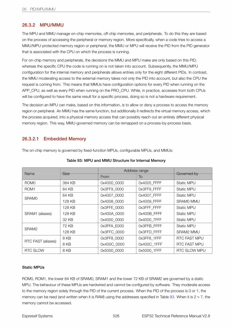
26. PID/MPU/MMU
26.3.2 MPU/MMU
The MPU and MMU manage on-chip memories, off-chip memories, and peripherals. To do this they are based
on the process of accessing the peripheral or memory region. More specifically, when a code tries to access a
MMU/MPU-protected memory region or peripheral, the MMU or MPU will receive the PID from the PID generator
that is associated with the CPU on which the process is running.
For on-chip memory and peripherals, the decisions the MMU and MPU make are only based on this PID,
whereas the specific CPU the code is running on is not taken into account. Subsequently, the MMU/MPU
configuration for the internal memory and peripherals allows entries only for the eight different PIDs. In contrast,
the MMU moderating access to the external memory takes not only the PID into account, but also the CPU the
request is coming from. This means that MMUs have configuration options for every PID when running on the
APP_CPU, as well as every PID when running on the PRO_CPU. While, in practice, accesses from both CPUs
will be configured to have the same result for a specific process, doing so is not a hardware requirement.
The decision an MPU can make, based on this information, is to allow or deny a process to access the memory
region or peripheral. An MMU has the same function, but additionally it redirects the virtual memory access, which
the process acquired, into a physical memory access that can possibly reach out an entirely different physical
memory region. This way, MMU-governed memory can be remapped on a process-by-process basis.
26.3.2.1 Embedded Memory
The on-chip memory is governed by fixed-function MPUs, configurable MPUs, and MMUs:
Table 93: MPU and MMU Structure for Internal Memory
Address rangeName Size
From ToGoverned by
ROM0 384 KB 0x4000_0000 0x4005_FFFF Static MPU
ROM1 64 KB 0x3FF9_0000 0x3FF9_FFFF Static MPU
SRAM064 KB 0x4007_0000 0x4007_FFFF Static MPU
128 KB 0x4008_0000 0x4009_FFFF SRAM0 MMU
SRAM1 (aliases)
128 KB 0x3FFE_0000 0x3FFF_FFFF Static MPU
128 KB 0x400A_0000 0x400B_FFFF Static MPU
32 KB 0x4000_0000 0x4000_7FFF Static MPU
SRAM272 KB 0x3FFA_E000 0x3FFB_FFFF Static MPU
128 KB 0x3FFC_0000 0x3FFD_FFFF SRAM2 MMU
RTC FAST (aliases)8 KB 0x3FF8_0000 0x3FF8_1FFF RTC FAST MPU
8 KB 0x400C_0000 0x400C_1FFF RTC FAST MPU
RTC SLOW 8 KB 0x5000_0000 0x5000_1FFF RTC SLOW MPU
Static MPUs
ROM0, ROM1, the lower 64 KB of SRAM0, SRAM1 and the lower 72 KB of SRAM2 are governed by a static
MPU. The behaviour of these MPUs are hardwired and cannot be configured by software. They moderate access
to the memory region solely through the PID of the current process. When the PID of the process is 0 or 1, the
memory can be read (and written when it is RAM) using the addresses specified in Table 93. When it is 2 ~ 7, the
memory cannot be accessed.
Espressif Systems 526 ESP32 Technical Reference Manual V2.8
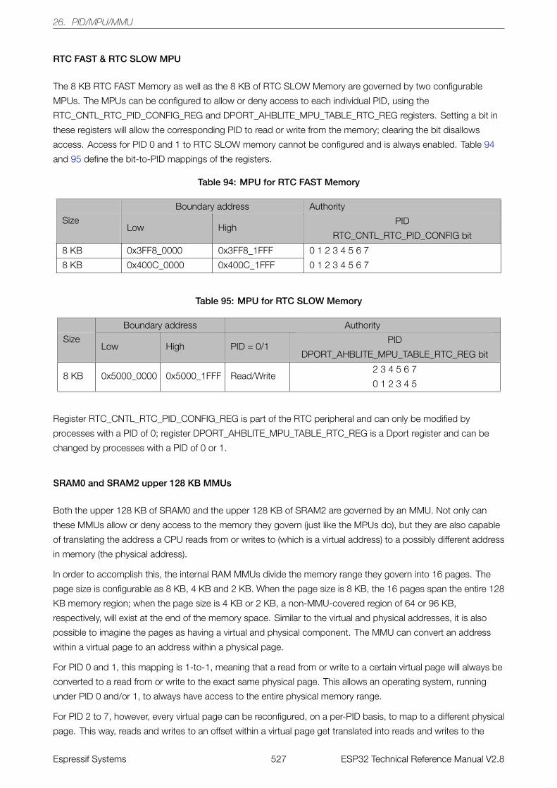
26. PID/MPU/MMU
RTC FAST & RTC SLOW MPU
The 8 KB RTC FAST Memory as well as the 8 KB of RTC SLOW Memory are governed by two configurable
MPUs. The MPUs can be configured to allow or deny access to each individual PID, using the
RTC_CNTL_RTC_PID_CONFIG_REG and DPORT_AHBLITE_MPU_TABLE_RTC_REG registers. Setting a bit in
these registers will allow the corresponding PID to read or write from the memory; clearing the bit disallows
access. Access for PID 0 and 1 to RTC SLOW memory cannot be configured and is always enabled. Table 94
and 95 define the bit-to-PID mappings of the registers.
Table 94: MPU for RTC FAST Memory
Boundary address Authority
SizeLow High
PID
RTC_CNTL_RTC_PID_CONFIG bit
8 KB 0x3FF8_0000 0x3FF8_1FFF 0 1 2 3 4 5 6 7
0 1 2 3 4 5 6 78 KB 0x400C_0000 0x400C_1FFF
Table 95: MPU for RTC SLOW Memory
Boundary address Authority
SizeLow High PID = 0/1
PID
DPORT_AHBLITE_MPU_TABLE_RTC_REG bit
8 KB 0x5000_0000 0x5000_1FFF Read/Write2 3 4 5 6 7
0 1 2 3 4 5
Register RTC_CNTL_RTC_PID_CONFIG_REG is part of the RTC peripheral and can only be modified by
processes with a PID of 0; register DPORT_AHBLITE_MPU_TABLE_RTC_REG is a Dport register and can be
changed by processes with a PID of 0 or 1.
SRAM0 and SRAM2 upper 128 KB MMUs
Both the upper 128 KB of SRAM0 and the upper 128 KB of SRAM2 are governed by an MMU. Not only can
these MMUs allow or deny access to the memory they govern (just like the MPUs do), but they are also capable
of translating the address a CPU reads from or writes to (which is a virtual address) to a possibly different address
in memory (the physical address).
In order to accomplish this, the internal RAM MMUs divide the memory range they govern into 16 pages. The
page size is configurable as 8 KB, 4 KB and 2 KB. When the page size is 8 KB, the 16 pages span the entire 128
KB memory region; when the page size is 4 KB or 2 KB, a non-MMU-covered region of 64 or 96 KB,
respectively, will exist at the end of the memory space. Similar to the virtual and physical addresses, it is also
possible to imagine the pages as having a virtual and physical component. The MMU can convert an address
within a virtual page to an address within a physical page.
For PID 0 and 1, this mapping is 1-to-1, meaning that a read from or write to a certain virtual page will always be
converted to a read from or write to the exact same physical page. This allows an operating system, running
under PID 0 and/or 1, to always have access to the entire physical memory range.
For PID 2 to 7, however, every virtual page can be reconfigured, on a per-PID basis, to map to a different physical
page. This way, reads and writes to an offset within a virtual page get translated into reads and writes to the
Espressif Systems 527 ESP32 Technical Reference Manual V2.8
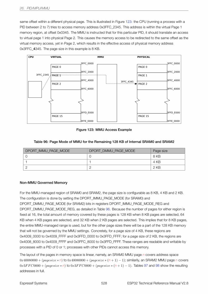
26. PID/MPU/MMU
same offset within a different physical page. This is illustrated in Figure 123: the CPU (running a process with a
PID between 2 to 7) tries to access memory address 0x3FFC_2345. This address is within the virtual Page 1
memory region, at offset 0x0345. The MMU is instructed that for this particular PID, it should translate an access
to virtual page 1 into physical Page 2. This causes the memory access to be redirected to the same offset as the
virtual memory access, yet in Page 2, which results in the effective access of physical memory address
0x3FFC_4345. The page size in this example is 8 KB.
PAGE 0
PAGE 1
PAGE 2
PAGE 15
3FFC_0000
3FFC_2000
3FFC_4000
3FFC_6000
3FFD_E000
3FFE_0000
PAGE 0
PAGE 1
PAGE 2
PAGE 15
3FFC_0000
3FFC_2000
3FFC_4000
3FFC_6000
3FFD_E000
3FFE_0000
VIRTUAL MMU PHYSICALCPU
3FFC_2345
3FFC_4345
Figure 123: MMU Access Example
Table 96: Page Mode of MMU for the Remaining 128 KB of Internal SRAM0 and SRAM2
DPORT_IMMU_PAGE_MODE DPORT_DMMU_PAGE_MODE Page size
0 0 8 KB
1 1 4 KB
2 2 2 KB
Non-MMU Governed Memory
For the MMU-managed region of SRAM0 and SRAM2, the page size is configurable as 8 KB, 4 KB and 2 KB.
The configuration is done by setting the DPORT_IMMU_PAGE_MODE (for SRAM0) and
DPORT_DMMU_PAGE_MODE (for SRAM2) bits in registers DPORT_IMMU_PAGE_MODE_REG and
DPORT_DMMU_PAGE_MODE_REG, as detailed in Table 96. Because the number of pages for either region is
fixed at 16, the total amount of memory covered by these pages is 128 KB when 8 KB pages are selected, 64
KB when 4 KB pages are selected, and 32 KB when 2 KB pages are selected. This implies that for 8 KB pages,
the entire MMU-managed range is used, but for the other page sizes there will be a part of the 128 KB memory
that will not be governed by the MMU settings. Concretely, for a page size of 4 KB, these regions are
0x4009_0000 to 0x4009_FFFF and 0x3FFD_0000 to 0x3FFD_FFFF; for a page size of 2 KB, the regions are
0x4008_8000 to 0x4009_FFFF and 0x3FFC_8000 to 0x3FFD_FFFF. These ranges are readable and writable by
processes with a PID of 0 or 1; processes with other PIDs cannot access this memory.
The layout of the pages in memory space is linear, namely, an SRAM0 MMU page n covers address space
0x40080000 + (pagesize ∗ n) to 0x40080000 + (pagesize ∗ (n+ 1)− 1); similarily, an SRAM2 MMU page n covers
0x3FFC0000 + (pagesize ∗ n) to 0x3FFC0000 + (pagesize ∗ (n+ 1)− 1). Tables 97 and 98 show the resulting
addresses in full.
Espressif Systems 528 ESP32 Technical Reference Manual V2.8
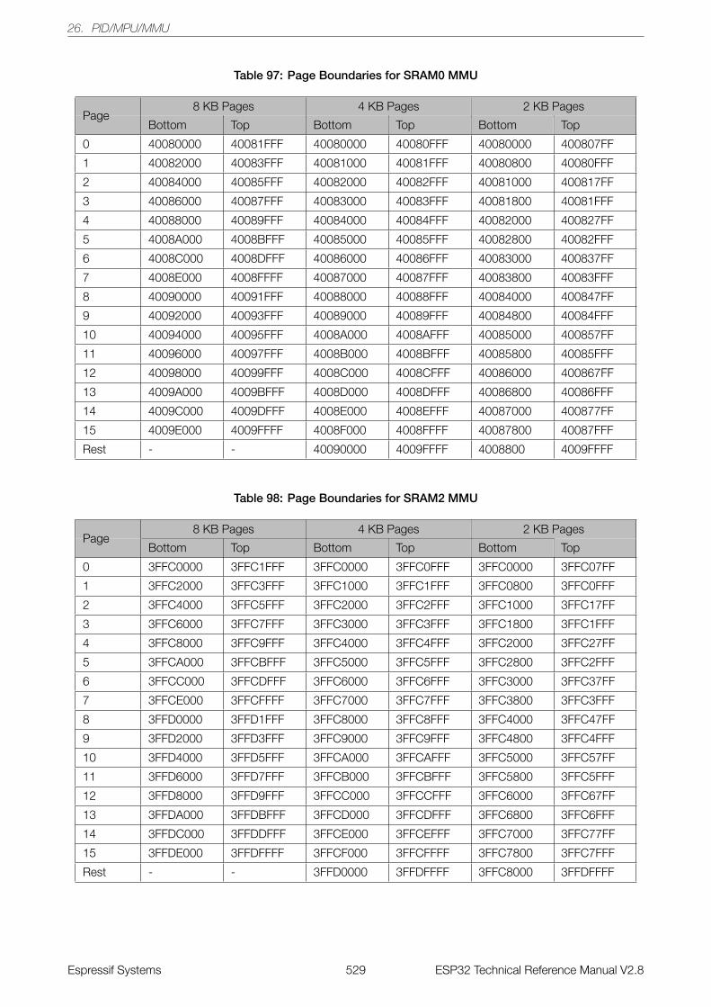
26. PID/MPU/MMU
Table 97: Page Boundaries for SRAM0 MMU
8 KB Pages 4 KB Pages 2 KB PagesPage
Bottom Top Bottom Top Bottom Top
0 40080000 40081FFF 40080000 40080FFF 40080000 400807FF
1 40082000 40083FFF 40081000 40081FFF 40080800 40080FFF
2 40084000 40085FFF 40082000 40082FFF 40081000 400817FF
3 40086000 40087FFF 40083000 40083FFF 40081800 40081FFF
4 40088000 40089FFF 40084000 40084FFF 40082000 400827FF
5 4008A000 4008BFFF 40085000 40085FFF 40082800 40082FFF
6 4008C000 4008DFFF 40086000 40086FFF 40083000 400837FF
7 4008E000 4008FFFF 40087000 40087FFF 40083800 40083FFF
8 40090000 40091FFF 40088000 40088FFF 40084000 400847FF
9 40092000 40093FFF 40089000 40089FFF 40084800 40084FFF
10 40094000 40095FFF 4008A000 4008AFFF 40085000 400857FF
11 40096000 40097FFF 4008B000 4008BFFF 40085800 40085FFF
12 40098000 40099FFF 4008C000 4008CFFF 40086000 400867FF
13 4009A000 4009BFFF 4008D000 4008DFFF 40086800 40086FFF
14 4009C000 4009DFFF 4008E000 4008EFFF 40087000 400877FF
15 4009E000 4009FFFF 4008F000 4008FFFF 40087800 40087FFF
Rest - - 40090000 4009FFFF 4008800 4009FFFF
Table 98: Page Boundaries for SRAM2 MMU
8 KB Pages 4 KB Pages 2 KB PagesPage
Bottom Top Bottom Top Bottom Top
0 3FFC0000 3FFC1FFF 3FFC0000 3FFC0FFF 3FFC0000 3FFC07FF
1 3FFC2000 3FFC3FFF 3FFC1000 3FFC1FFF 3FFC0800 3FFC0FFF
2 3FFC4000 3FFC5FFF 3FFC2000 3FFC2FFF 3FFC1000 3FFC17FF
3 3FFC6000 3FFC7FFF 3FFC3000 3FFC3FFF 3FFC1800 3FFC1FFF
4 3FFC8000 3FFC9FFF 3FFC4000 3FFC4FFF 3FFC2000 3FFC27FF
5 3FFCA000 3FFCBFFF 3FFC5000 3FFC5FFF 3FFC2800 3FFC2FFF
6 3FFCC000 3FFCDFFF 3FFC6000 3FFC6FFF 3FFC3000 3FFC37FF
7 3FFCE000 3FFCFFFF 3FFC7000 3FFC7FFF 3FFC3800 3FFC3FFF
8 3FFD0000 3FFD1FFF 3FFC8000 3FFC8FFF 3FFC4000 3FFC47FF
9 3FFD2000 3FFD3FFF 3FFC9000 3FFC9FFF 3FFC4800 3FFC4FFF
10 3FFD4000 3FFD5FFF 3FFCA000 3FFCAFFF 3FFC5000 3FFC57FF
11 3FFD6000 3FFD7FFF 3FFCB000 3FFCBFFF 3FFC5800 3FFC5FFF
12 3FFD8000 3FFD9FFF 3FFCC000 3FFCCFFF 3FFC6000 3FFC67FF
13 3FFDA000 3FFDBFFF 3FFCD000 3FFCDFFF 3FFC6800 3FFC6FFF
14 3FFDC000 3FFDDFFF 3FFCE000 3FFCEFFF 3FFC7000 3FFC77FF
15 3FFDE000 3FFDFFFF 3FFCF000 3FFCFFFF 3FFC7800 3FFC7FFF
Rest - - 3FFD0000 3FFDFFFF 3FFC8000 3FFDFFFF
Espressif Systems 529 ESP32 Technical Reference Manual V2.8
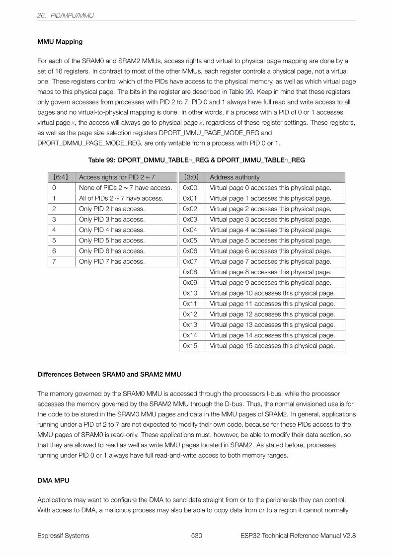
26. PID/MPU/MMU
MMU Mapping
For each of the SRAM0 and SRAM2 MMUs, access rights and virtual to physical page mapping are done by a
set of 16 registers. In contrast to most of the other MMUs, each register controls a physical page, not a virtual
one. These registers control which of the PIDs have access to the physical memory, as well as which virtual page
maps to this physical page. The bits in the register are described in Table 99. Keep in mind that these registers
only govern accesses from processes with PID 2 to 7; PID 0 and 1 always have full read and write access to all
pages and no virtual-to-physical mapping is done. In other words, if a process with a PID of 0 or 1 accesses
virtual page x, the access will always go to physical page x, regardless of these register settings. These registers,
as well as the page size selection registers DPORT_IMMU_PAGE_MODE_REG and
DPORT_DMMU_PAGE_MODE_REG, are only writable from a process with PID 0 or 1.
Table 99: DPORT_DMMU_TABLEn_REG & DPORT_IMMU_TABLEn_REG
[6:4] Access rights for PID 2 ~ 7
0 None of PIDs 2 ~ 7 have access.
1 All of PIDs 2 ~ 7 have access.
2 Only PID 2 has access.
3 Only PID 3 has access.
4 Only PID 4 has access.
5 Only PID 5 has access.
6 Only PID 6 has access.
7 Only PID 7 has access.
[3:0] Address authority
0x00 Virtual page 0 accesses this physical page.
0x01 Virtual page 1 accesses this physical page.
0x02 Virtual page 2 accesses this physical page.
0x03 Virtual page 3 accesses this physical page.
0x04 Virtual page 4 accesses this physical page.
0x05 Virtual page 5 accesses this physical page.
0x06 Virtual page 6 accesses this physical page.
0x07 Virtual page 7 accesses this physical page.
0x08 Virtual page 8 accesses this physical page.
0x09 Virtual page 9 accesses this physical page.
0x10 Virtual page 10 accesses this physical page.
0x11 Virtual page 11 accesses this physical page.
0x12 Virtual page 12 accesses this physical page.
0x13 Virtual page 13 accesses this physical page.
0x14 Virtual page 14 accesses this physical page.
0x15 Virtual page 15 accesses this physical page.
Differences Between SRAM0 and SRAM2 MMU
The memory governed by the SRAM0 MMU is accessed through the processors I-bus, while the processor
accesses the memory governed by the SRAM2 MMU through the D-bus. Thus, the normal envisioned use is for
the code to be stored in the SRAM0 MMU pages and data in the MMU pages of SRAM2. In general, applications
running under a PID of 2 to 7 are not expected to modify their own code, because for these PIDs access to the
MMU pages of SRAM0 is read-only. These applications must, however, be able to modify their data section, so
that they are allowed to read as well as write MMU pages located in SRAM2. As stated before, processes
running under PID 0 or 1 always have full read-and-write access to both memory ranges.
DMA MPU
Applications may want to configure the DMA to send data straight from or to the peripherals they can control.
With access to DMA, a malicious process may also be able to copy data from or to a region it cannot normally
Espressif Systems 530 ESP32 Technical Reference Manual V2.8
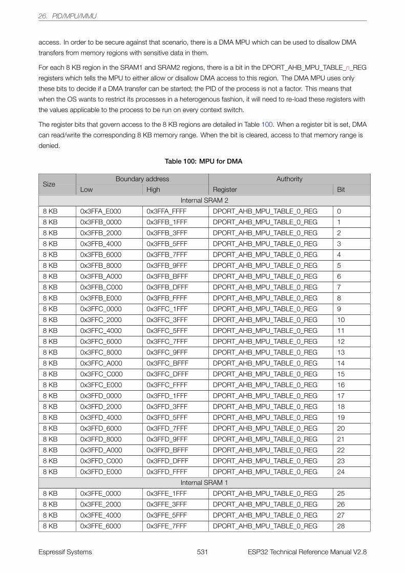
26. PID/MPU/MMU
access. In order to be secure against that scenario, there is a DMA MPU which can be used to disallow DMA
transfers from memory regions with sensitive data in them.
For each 8 KB region in the SRAM1 and SRAM2 regions, there is a bit in the DPORT_AHB_MPU_TABLE_n_REG
registers which tells the MPU to either allow or disallow DMA access to this region. The DMA MPU uses only
these bits to decide if a DMA transfer can be started; the PID of the process is not a factor. This means that
when the OS wants to restrict its processes in a heterogenous fashion, it will need to re-load these registers with
the values applicable to the process to be run on every context switch.
The register bits that govern access to the 8 KB regions are detailed in Table 100. When a register bit is set, DMA
can read/write the corresponding 8 KB memory range. When the bit is cleared, access to that memory range is
denied.
Table 100: MPU for DMA
Boundary address AuthoritySize
Low High Register Bit
Internal SRAM 2
8 KB 0x3FFA_E000 0x3FFA_FFFF DPORT_AHB_MPU_TABLE_0_REG 0
8 KB 0x3FFB_0000 0x3FFB_1FFF DPORT_AHB_MPU_TABLE_0_REG 1
8 KB 0x3FFB_2000 0x3FFB_3FFF DPORT_AHB_MPU_TABLE_0_REG 2
8 KB 0x3FFB_4000 0x3FFB_5FFF DPORT_AHB_MPU_TABLE_0_REG 3
8 KB 0x3FFB_6000 0x3FFB_7FFF DPORT_AHB_MPU_TABLE_0_REG 4
8 KB 0x3FFB_8000 0x3FFB_9FFF DPORT_AHB_MPU_TABLE_0_REG 5
8 KB 0x3FFB_A000 0x3FFB_BFFF DPORT_AHB_MPU_TABLE_0_REG 6
8 KB 0x3FFB_C000 0x3FFB_DFFF DPORT_AHB_MPU_TABLE_0_REG 7
8 KB 0x3FFB_E000 0x3FFB_FFFF DPORT_AHB_MPU_TABLE_0_REG 8
8 KB 0x3FFC_0000 0x3FFC_1FFF DPORT_AHB_MPU_TABLE_0_REG 9
8 KB 0x3FFC_2000 0x3FFC_3FFF DPORT_AHB_MPU_TABLE_0_REG 10
8 KB 0x3FFC_4000 0x3FFC_5FFF DPORT_AHB_MPU_TABLE_0_REG 11
8 KB 0x3FFC_6000 0x3FFC_7FFF DPORT_AHB_MPU_TABLE_0_REG 12
8 KB 0x3FFC_8000 0x3FFC_9FFF DPORT_AHB_MPU_TABLE_0_REG 13
8 KB 0x3FFC_A000 0x3FFC_BFFF DPORT_AHB_MPU_TABLE_0_REG 14
8 KB 0x3FFC_C000 0x3FFC_DFFF DPORT_AHB_MPU_TABLE_0_REG 15
8 KB 0x3FFC_E000 0x3FFC_FFFF DPORT_AHB_MPU_TABLE_0_REG 16
8 KB 0x3FFD_0000 0x3FFD_1FFF DPORT_AHB_MPU_TABLE_0_REG 17
8 KB 0x3FFD_2000 0x3FFD_3FFF DPORT_AHB_MPU_TABLE_0_REG 18
8 KB 0x3FFD_4000 0x3FFD_5FFF DPORT_AHB_MPU_TABLE_0_REG 19
8 KB 0x3FFD_6000 0x3FFD_7FFF DPORT_AHB_MPU_TABLE_0_REG 20
8 KB 0x3FFD_8000 0x3FFD_9FFF DPORT_AHB_MPU_TABLE_0_REG 21
8 KB 0x3FFD_A000 0x3FFD_BFFF DPORT_AHB_MPU_TABLE_0_REG 22
8 KB 0x3FFD_C000 0x3FFD_DFFF DPORT_AHB_MPU_TABLE_0_REG 23
8 KB 0x3FFD_E000 0x3FFD_FFFF DPORT_AHB_MPU_TABLE_0_REG 24
Internal SRAM 1
8 KB 0x3FFE_0000 0x3FFE_1FFF DPORT_AHB_MPU_TABLE_0_REG 25
8 KB 0x3FFE_2000 0x3FFE_3FFF DPORT_AHB_MPU_TABLE_0_REG 26
8 KB 0x3FFE_4000 0x3FFE_5FFF DPORT_AHB_MPU_TABLE_0_REG 27
8 KB 0x3FFE_6000 0x3FFE_7FFF DPORT_AHB_MPU_TABLE_0_REG 28
Espressif Systems 531 ESP32 Technical Reference Manual V2.8

26. PID/MPU/MMU
Boundary address AuthoritySize
Low High Register Bit
8 KB 0x3FFE_8000 0x3FFE_9FFF DPORT_AHB_MPU_TABLE_0_REG 29
8 KB 0x3FFE_A000 0x3FFE_BFFF DPORT_AHB_MPU_TABLE_0_REG 30
8 KB 0x3FFE_C000 0x3FFE_DFFF DPORT_AHB_MPU_TABLE_0_REG 31
8 KB 0x3FFE_E000 0x3FFE_FFFF DPORT_AHB_MPU_TABLE_1_REG 0
8 KB 0x3FFF_0000 0x3FFF_1FFF DPORT_AHB_MPU_TABLE_1_REG 1
8 KB 0x3FFF_2000 0x3FFF_3FFF DPORT_AHB_MPU_TABLE_1_REG 2
8 KB 0x3FFF_4000 0x3FFF_5FFF DPORT_AHB_MPU_TABLE_1_REG 3
8 KB 0x3FFF_6000 0x3FFF_7FFF DPORT_AHB_MPU_TABLE_1_REG 4
8 KB 0x3FFF_8000 0x3FFF_9FFF DPORT_AHB_MPU_TABLE_1_REG 5
8 KB 0x3FFF_A000 0x3FFF_BFFF DPORT_AHB_MPU_TABLE_1_REG 6
8 KB 0x3FFF_C000 0x3FFF_DFFF DPORT_AHB_MPU_TABLE_1_REG 7
8 KB 0x3FFF_E000 0x3FFF_FFFF DPORT_AHB_MPU_TABLE_1_REG 8
Registers DPROT_AHB_MPU_TABLE_0_REG�DPROT_AHB_MPU_TABLE_1_REG are located in the DPort
address space. Only processes with a PID of 0 or 1 can modify these two registers.
26.3.2.2 External Memory
Accesses to the external flash and external SPI RAM are done through a cache and are also handled by an
MMU. This Cache MMU can apply different mappings, depending on the PID of the process as well as the CPU
the process is running on. The MMU does this in a way that is similar to the internal memory MMU, that is, for
every page of virtual memory, it has a register detailing which physical page this virtual page should map to.
There are differences between the MMUs governing the internal memory and the Cache MMU, though. First of
all, the Cache MMU has a fixed page size (which is 64 KB for external flash and 32 KB for external RAM) and
secondly, instead of specifying access rights in the MMU entries, the Cache MMU has explicit mapping tables for
each PID and processor core. The MMU mapping configuration registers will be referred to as ’entries’ in the rest
of this chapter. These registers are only accessible from processes with a PID of 0 or 1; processes with a PID of 2
to 7 will have to delegate to one of the above-mentioned processes to change their MMU settings.
The MMU entries, as stated before, are used for mapping a virtual memory page access to a physical memory
page access. The MMU controls five regions of virtual address space, detailed in Table 101. V Addr1 to V Addr4
are used for accessing external flash, whereas V AddrRAM is used for accessing external RAM. Note that
V Addr4 is a subset of V Addr0.
Espressif Systems 532 ESP32 Technical Reference Manual V2.8
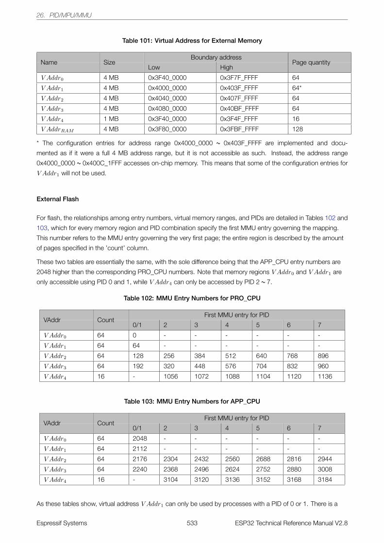
26. PID/MPU/MMU
Table 101: Virtual Address for External Memory
Boundary addressName Size
Low HighPage quantity
V Addr0 4 MB 0x3F40_0000 0x3F7F_FFFF 64
V Addr1 4 MB 0x4000_0000 0x403F_FFFF 64*
V Addr2 4 MB 0x4040_0000 0x407F_FFFF 64
V Addr3 4 MB 0x4080_0000 0x40BF_FFFF 64
V Addr4 1 MB 0x3F40_0000 0x3F4F_FFFF 16
V AddrRAM 4 MB 0x3F80_0000 0x3FBF_FFFF 128
* The configuration entries for address range 0x4000_0000 ~ 0x403F_FFFF are implemented and docu-
mented as if it were a full 4 MB address range, but it is not accessible as such. Instead, the address range
0x4000_0000 ~ 0x400C_1FFF accesses on-chip memory. This means that some of the configuration entries for
V Addr1 will not be used.
External Flash
For flash, the relationships among entry numbers, virtual memory ranges, and PIDs are detailed in Tables 102 and
103, which for every memory region and PID combination specify the first MMU entry governing the mapping.
This number refers to the MMU entry governing the very first page; the entire region is described by the amount
of pages specified in the ’count’ column.
These two tables are essentially the same, with the sole difference being that the APP_CPU entry numbers are
2048 higher than the corresponding PRO_CPU numbers. Note that memory regions V Addr0 and V Addr1 are
only accessible using PID 0 and 1, while V Addr4 can only be accessed by PID 2 ~ 7.
Table 102: MMU Entry Numbers for PRO_CPU
First MMU entry for PIDVAddr Count
0/1 2 3 4 5 6 7
V Addr0 64 0 - - - - - -
V Addr1 64 64 - - - - - -
V Addr2 64 128 256 384 512 640 768 896
V Addr3 64 192 320 448 576 704 832 960
V Addr4 16 - 1056 1072 1088 1104 1120 1136
Table 103: MMU Entry Numbers for APP_CPU
First MMU entry for PIDVAddr Count
0/1 2 3 4 5 6 7
V Addr0 64 2048 - - - - - -
V Addr1 64 2112 - - - - - -
V Addr2 64 2176 2304 2432 2560 2688 2816 2944
V Addr3 64 2240 2368 2496 2624 2752 2880 3008
V Addr4 16 - 3104 3120 3136 3152 3168 3184
As these tables show, virtual address V Addr1 can only be used by processes with a PID of 0 or 1. There is a
Espressif Systems 533 ESP32 Technical Reference Manual V2.8
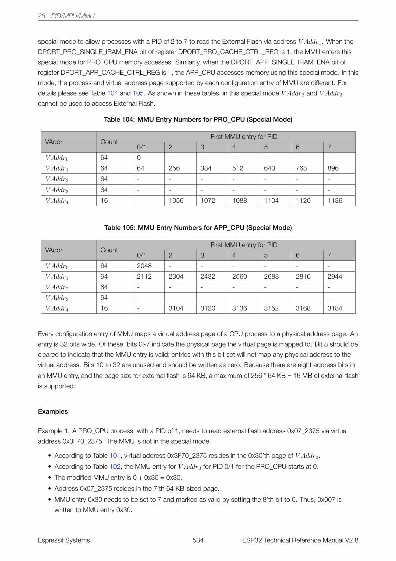
26. PID/MPU/MMU
special mode to allow processes with a PID of 2 to 7 to read the External Flash via address V Addr1. When the
DPORT_PRO_SINGLE_IRAM_ENA bit of register DPORT_PRO_CACHE_CTRL_REG is 1, the MMU enters this
special mode for PRO_CPU memory accesses. Similarily, when the DPORT_APP_SINGLE_IRAM_ENA bit of
register DPORT_APP_CACHE_CTRL_REG is 1, the APP_CPU accesses memory using this special mode. In this
mode, the process and virtual address page supported by each configuration entry of MMU are different. For
details please see Table 104 and 105. As shown in these tables, in this special mode V Addr2 and V Addr3
cannot be used to access External Flash.
Table 104: MMU Entry Numbers for PRO_CPU (Special Mode)
First MMU entry for PIDVAddr Count
0/1 2 3 4 5 6 7
V Addr0 64 0 - - - - - -
V Addr1 64 64 256 384 512 640 768 896
V Addr2 64 - - - - - - -
V Addr3 64 - - - - - - -
V Addr4 16 - 1056 1072 1088 1104 1120 1136
Table 105: MMU Entry Numbers for APP_CPU (Special Mode)
First MMU entry for PIDVAddr Count
0/1 2 3 4 5 6 7
V Addr0 64 2048 - - - - - -
V Addr1 64 2112 2304 2432 2560 2688 2816 2944
V Addr2 64 - - - - - - -
V Addr3 64 - - - - - - -
V Addr4 16 - 3104 3120 3136 3152 3168 3184
Every configuration entry of MMU maps a virtual address page of a CPU process to a physical address page. An
entry is 32 bits wide. Of these, bits 0~7 indicate the physical page the virtual page is mapped to. Bit 8 should be
cleared to indicate that the MMU entry is valid; entries with this bit set will not map any physical address to the
virtual address. Bits 10 to 32 are unused and should be written as zero. Because there are eight address bits in
an MMU entry, and the page size for external flash is 64 KB, a maximum of 256 * 64 KB = 16 MB of external flash
is supported.
Examples
Example 1. A PRO_CPU process, with a PID of 1, needs to read external flash address 0x07_2375 via virtual
address 0x3F70_2375. The MMU is not in the special mode.
• According to Table 101, virtual address 0x3F70_2375 resides in the 0x30’th page of V Addr0.
• According to Table 102, the MMU entry for V Addr0 for PID 0/1 for the PRO_CPU starts at 0.
• The modified MMU entry is 0 + 0x30 = 0x30.
• Address 0x07_2375 resides in the 7’th 64 KB-sized page.
• MMU entry 0x30 needs to be set to 7 and marked as valid by setting the 8’th bit to 0. Thus, 0x007 is
written to MMU entry 0x30.
Espressif Systems 534 ESP32 Technical Reference Manual V2.8
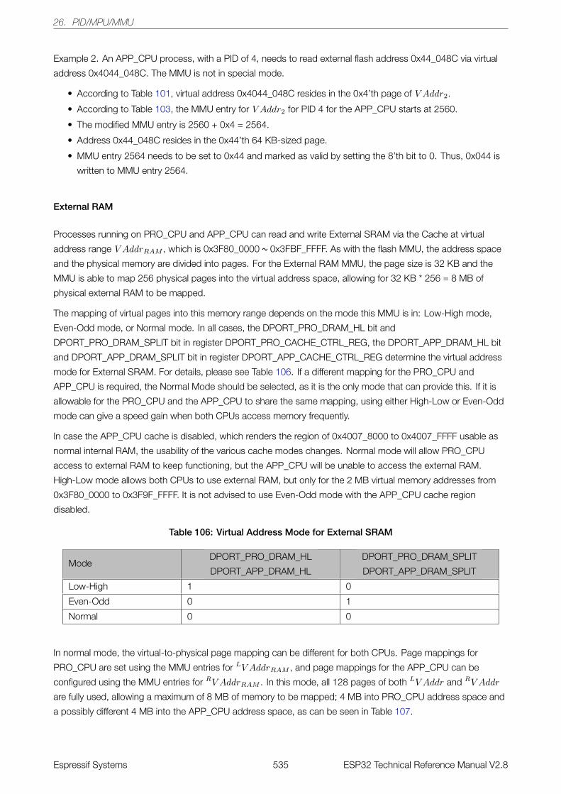
26. PID/MPU/MMU
Example 2. An APP_CPU process, with a PID of 4, needs to read external flash address 0x44_048C via virtual
address 0x4044_048C. The MMU is not in special mode.
• According to Table 101, virtual address 0x4044_048C resides in the 0x4’th page of V Addr2.
• According to Table 103, the MMU entry for V Addr2 for PID 4 for the APP_CPU starts at 2560.
• The modified MMU entry is 2560 + 0x4 = 2564.
• Address 0x44_048C resides in the 0x44’th 64 KB-sized page.
• MMU entry 2564 needs to be set to 0x44 and marked as valid by setting the 8’th bit to 0. Thus, 0x044 is
written to MMU entry 2564.
External RAM
Processes running on PRO_CPU and APP_CPU can read and write External SRAM via the Cache at virtual
address range V AddrRAM , which is 0x3F80_0000 ~ 0x3FBF_FFFF. As with the flash MMU, the address space
and the physical memory are divided into pages. For the External RAM MMU, the page size is 32 KB and the
MMU is able to map 256 physical pages into the virtual address space, allowing for 32 KB * 256 = 8 MB of
physical external RAM to be mapped.
The mapping of virtual pages into this memory range depends on the mode this MMU is in: Low-High mode,
Even-Odd mode, or Normal mode. In all cases, the DPORT_PRO_DRAM_HL bit and
DPORT_PRO_DRAM_SPLIT bit in register DPORT_PRO_CACHE_CTRL_REG, the DPORT_APP_DRAM_HL bit
and DPORT_APP_DRAM_SPLIT bit in register DPORT_APP_CACHE_CTRL_REG determine the virtual address
mode for External SRAM. For details, please see Table 106. If a different mapping for the PRO_CPU and
APP_CPU is required, the Normal Mode should be selected, as it is the only mode that can provide this. If it is
allowable for the PRO_CPU and the APP_CPU to share the same mapping, using either High-Low or Even-Odd
mode can give a speed gain when both CPUs access memory frequently.
In case the APP_CPU cache is disabled, which renders the region of 0x4007_8000 to 0x4007_FFFF usable as
normal internal RAM, the usability of the various cache modes changes. Normal mode will allow PRO_CPU
access to external RAM to keep functioning, but the APP_CPU will be unable to access the external RAM.
High-Low mode allows both CPUs to use external RAM, but only for the 2 MB virtual memory addresses from
0x3F80_0000 to 0x3F9F_FFFF. It is not advised to use Even-Odd mode with the APP_CPU cache region
disabled.
Table 106: Virtual Address Mode for External SRAM
ModeDPORT_PRO_DRAM_HL
DPORT_APP_DRAM_HL
DPORT_PRO_DRAM_SPLIT
DPORT_APP_DRAM_SPLIT
Low-High 1 0
Even-Odd 0 1
Normal 0 0
In normal mode, the virtual-to-physical page mapping can be different for both CPUs. Page mappings for
PRO_CPU are set using the MMU entries for LV AddrRAM , and page mappings for the APP_CPU can be
configured using the MMU entries for RV AddrRAM . In this mode, all 128 pages of both LV Addr and RV Addr
are fully used, allowing a maximum of 8 MB of memory to be mapped; 4 MB into PRO_CPU address space and
a possibly different 4 MB into the APP_CPU address space, as can be seen in Table 107.
Espressif Systems 535 ESP32 Technical Reference Manual V2.8
26. PID/MPU/MMU
Table 107: Virtual Address for External SRAM ( Normal Mode )
PRO_CPU addressVirtual address Size
Low HighLV AddrRAM 4 MB 0x3F80_0000 0x3FBF_FFFF
APP_CPU addressVirtual address Size
Low HighRV AddrRAM 4 MB 0x3F80_0000 0x3FBF_FFFF
In Low-High mode, both the PRO_CPU and the APP_CPU use the same mapping entries. In this modeLV AddrRAM is used for the lower 2 MB of the virtual address space, while RV AddrRAM is used for the upper 2
MB. This also means that the upper 64 MMU entries for LV AddrRAM , as well as the lower 64 entries forRV AddrRAM , are unused. Table 108 details these address ranges.
Table 108: Virtual Address for External SRAM ( Low-High Mode )
PRO_CPU/APP_CPU addressVirtual address Size
Low HighLV AddrRAM 2 MB 0x3F80_0000 0x3F9F_FFFFRV AddrRAM 2 MB 0x3FA0_0000 0x3FBF_FFFF
In Even-Odd memory, the VRAM is split into 32-byte chunks. The even chunks are resolved through the MMU
entries for LV AddrRAM , the odd chunks through the entries for RV AddrRAM . Generally, the MMU entries forLV AddrRAM and RV AddrRAM are set to the same values, so that the virtual pages map to a contiguous region
of physical memory. Table 109 details this mode.
Table 109: Virtual Address for External SRAM ( Even-Odd Mode )
PRO_CPU/APP_CPU addressVirtual address Size
Low HighLV AddrRAM 32 Bytes 0x3F80_0000 0x3F80_001FRV AddrRAM 32 Bytes 0x3F80_0020 0x3F80_003FLV AddrRAM 32 Bytes 0x3F80_0040 0x3F80_005FRV AddrRAM 32 Bytes 0x3F80_0060 0x3F80_007F
· · ·LV AddrRAM 32 Bytes 0x3FBF_FFC0 0x3FBF_FFDFRV AddrRAM 32 Bytes 0x3FBF_FFE0 0x3FBF_FFFF
The bit configuration of the External RAM MMU entries is the same as for the flash memory: the entries are 32-bit
registers, with the lower nine bits being used. Bits 0~7 contain the physical page the entry should map its
associate virtual page address to, while bit 8 is cleared when the entry is valid and set when it is not. Table 110
details the first MMU entry number for LV AddrRAM and RV AddrRAM for all PIDs.
Espressif Systems 536 ESP32 Technical Reference Manual V2.8
26. PID/MPU/MMU
Table 110: MMU Entry Numbers for External RAM
First MMU entry for PIDVAddr Count
0/1 2 3 4 5 6 7LV AddrRAM 128 1152 1280 1408 1536 1664 1792 1920RV AddrRAM 128 3200 3328 3456 3584 3712 3840 3968
Examples
Example 1. A PRO_CPU process, with a PID of 7, needs to read or write external RAM address 0x7F_A375 via
virtual address 0x3FA7_2375. The MMU is in Low-High mode.
• According to Table 101, virtual address 0x3FA7_2375 resides in the 0x4E’th 32-KB-page of V AddrRAM .
• According to Table 108, virtual address 0x3FA7_2375 is governed by RV AddrRAM .
• According to Table 110, the MMU entry for RV AddrRAM for PID 7 for the PRO_CPU starts at 3968.
• The modified MMU entry is 3968 + 0x4E = 4046.
• Address 0x7F_A375 resides in the 255’th 32 KB-sized page.
• MMU entry 4046 needs to be set to 255 and marked as valid by clearing the 8’th bit. Thus, 0x0FF is written
to MMU entry 4046.
Example 2. An APP_CPU process, with a PID of 5, needs to read or write external RAM address 0x55_5805 up
to 0x55_5823 starting at virtual address 0x3F85_5805. The MMU is in Even-Odd mode.
• According to Table 101, virtual address 0x3F85_5805 resides in the 0x0A’th 32-KB-page of V AddrRAM .
• According to Table 109, the range to be read/written spans both a 32-byte region in RV AddrRAM andLV AddrRAM .
• According to Table 110, the MMU entry for LV AddrRAM for PID 5 starts at 1664.
• According to Table 110, the MMU entry for RV AddrRAM for PID 5 starts at 3712.
• The modified MMU entries are 1664 + 0x0A = 1674 and 3712 + 0x0A = 3722.
• The addresses 0x55_5805 to 0x55_5823 reside in the 0xAA’th 32 KB-sized page.
• MMU entries 1674 and 3722 need to be set to 0xAA and marked as valid by setting the 8’th bit to 0. Thus,
0x0AA is written to MMU entries 1674 and 3722. This mapping applies to both the PRO_CPU and the
APP_CPU.
Example 3. A PRO_CPU process, with a PID of 1, and an APP_CPU process whose PID is also 1, need to read
or write external RAM using virtual address 0x3F80_0876. The PRO_CPU needs this region to access physical
address 0x10_0876, while the APP_CPU wants to access physical address 0x20_0876 through this virtual
address. The MMU is in Normal mode.
• According to Table 101, virtual address 0x3F80_0876 resides in the 0’th 32-KB-page of V AddrRAM .
• According to Table 110, the MMU entry for PID 1 for the PRO_CPU starts at 1152.
• According to Table 110, the MMU entry for PID 1 for the APP_CPU starts at 3200.
• The MMU entries that are modified are 1152 + 0 = 1152 for the PRO_CPU and 3200 + 0 = 3200 for the
APP_CPU.
• Address 0x10_0876 resides in the 0x20’th 32 KB-sized page.
• Address 0x20_0876 resides in the 0x40’th 32 KB-sized page.
• For the PRO_CPU, MMU entry 1152 needs to be set to 0x20 and marked as valid by clearing the 8’th bit.
Thus, 0x020 is written to MMU entry 1152.
Espressif Systems 537 ESP32 Technical Reference Manual V2.8
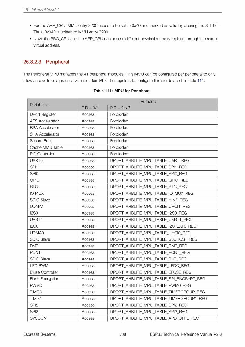
26. PID/MPU/MMU
• For the APP_CPU, MMU entry 3200 needs to be set to 0x40 and marked as valid by clearing the 8’th bit.
Thus, 0x040 is written to MMU entry 3200.
• Now, the PRO_CPU and the APP_CPU can access different physical memory regions through the same
virtual address.
26.3.2.3 Peripheral
The Peripheral MPU manages the 41 peripheral modules. This MMU can be configured per peripheral to only
allow access from a process with a certain PID. The registers to configure this are detailed in Table 111.
Table 111: MPU for Peripheral
AuthorityPeripheral
PID = 0/1 PID = 2 ~ 7
DPort Register Access Forbidden
AES Accelerator Access Forbidden
RSA Accelerator Access Forbidden
SHA Accelerator Access Forbidden
Secure Boot Access Forbidden
Cache MMU Table Access Forbidden
PID Controller Access Forbidden
UART0 Access DPORT_AHBLITE_MPU_TABLE_UART_REG
SPI1 Access DPORT_AHBLITE_MPU_TABLE_SPI1_REG
SPI0 Access DPORT_AHBLITE_MPU_TABLE_SPI0_REG
GPIO Access DPORT_AHBLITE_MPU_TABLE_GPIO_REG
RTC Access DPORT_AHBLITE_MPU_TABLE_RTC_REG
IO MUX Access DPORT_AHBLITE_MPU_TABLE_IO_MUX_REG
SDIO Slave Access DPORT_AHBLITE_MPU_TABLE_HINF_REG
UDMA1 Access DPORT_AHBLITE_MPU_TABLE_UHCI1_REG
I2S0 Access DPORT_AHBLITE_MPU_TABLE_I2S0_REG
UART1 Access DPORT_AHBLITE_MPU_TABLE_UART1_REG
I2C0 Access DPORT_AHBLITE_MPU_TABLE_I2C_EXT0_REG
UDMA0 Access DPORT_AHBLITE_MPU_TABLE_UHCI0_REG
SDIO Slave Access DPORT_AHBLITE_MPU_TABLE_SLCHOST_REG
RMT Access DPORT_AHBLITE_MPU_TABLE_RMT_REG
PCNT Access DPORT_AHBLITE_MPU_TABLE_PCNT_REG
SDIO Slave Access DPORT_AHBLITE_MPU_TABLE_SLC_REG
LED PWM Access DPORT_AHBLITE_MPU_TABLE_LEDC_REG
Efuse Controller Access DPORT_AHBLITE_MPU_TABLE_EFUSE_REG
Flash Encryption Access DPORT_AHBLITE_MPU_TABLE_SPI_ENCRYPT_REG
PWM0 Access DPORT_AHBLITE_MPU_TABLE_PWM0_REG
TIMG0 Access DPORT_AHBLITE_MPU_TABLE_TIMERGROUP_REG
TIMG1 Access DPORT_AHBLITE_MPU_TABLE_TIMERGROUP1_REG
SPI2 Access DPORT_AHBLITE_MPU_TABLE_SPI2_REG
SPI3 Access DPORT_AHBLITE_MPU_TABLE_SPI3_REG
SYSCON Access DPORT_AHBLITE_MPU_TABLE_APB_CTRL_REG
Espressif Systems 538 ESP32 Technical Reference Manual V2.8
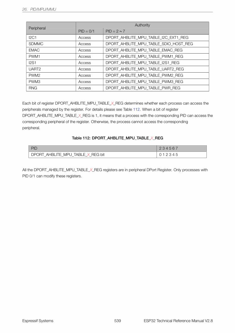
26. PID/MPU/MMU
AuthorityPeripheral
PID = 0/1 PID = 2 ~ 7
I2C1 Access DPORT_AHBLITE_MPU_TABLE_I2C_EXT1_REG
SDMMC Access DPORT_AHBLITE_MPU_TABLE_SDIO_HOST_REG
EMAC Access DPORT_AHBLITE_MPU_TABLE_EMAC_REG
PWM1 Access DPORT_AHBLITE_MPU_TABLE_PWM1_REG
I2S1 Access DPORT_AHBLITE_MPU_TABLE_I2S1_REG
UART2 Access DPORT_AHBLITE_MPU_TABLE_UART2_REG
PWM2 Access DPORT_AHBLITE_MPU_TABLE_PWM2_REG
PWM3 Access DPORT_AHBLITE_MPU_TABLE_PWM3_REG
RNG Access DPORT_AHBLITE_MPU_TABLE_PWR_REG
Each bit of register DPORT_AHBLITE_MPU_TABLE_X_REG determines whether each process can access the
peripherals managed by the register. For details please see Table 112. When a bit of register
DPORT_AHBLITE_MPU_TABLE_X_REG is 1, it means that a process with the corresponding PID can access the
corresponding peripheral of the register. Otherwise, the process cannot access the corresponding
peripheral.
Table 112: DPORT_AHBLITE_MPU_TABLE_X_REG
PID 2 3 4 5 6 7
DPORT_AHBLITE_MPU_TABLE_X_REG bit 0 1 2 3 4 5
All the DPORT_AHBLITE_MPU_TABLE_X_REG registers are in peripheral DPort Register. Only processes with
PID 0/1 can modify these registers.
Espressif Systems 539 ESP32 Technical Reference Manual V2.8
27. PID CONTROLLER
27. PID Controller
27.1 Overview
The ESP32 is a dual core device and is capable of running and managing multiple processes. The PID Controller
supports switching of PID when a process switch occurs. In addition to PID management, the PID Controller also
facilitates management of nested interrupts by recording execution status just before an interrupt service routine
is executed. This enables the user application to manage process switches and nested interrupts more
efficiently.
27.2 Features
The PID Controller features:
• Process management and priority
• Process PID switch
• Interrupt information recording
• Nested interrupt management
27.3 Functional Description
Eight processes run on the CPU, and are assigned with PID of 0 ~ 7 respectively. Among the eight processes,
processes with PID of 0 or 1 are elevated processes with higher authority compared to processes with PID
ranging from 2 ~ 7.
A CPU process switch may occur in two cases:
• An interrupt occurs and the CPU fetches an instruction from the interrupt vector. Instruction fetch or
execution from interrupt vector is always treated as a process with PID of 0, irrespective of which process
was being executed on the CPU when the interrupt occurred.
• A currently active process explicitly performs a process switch. Only elevated processes with PID of 0 or 1
may perform a process switch.
Espressif Systems 540 ESP32 Technical Reference Manual V2.8
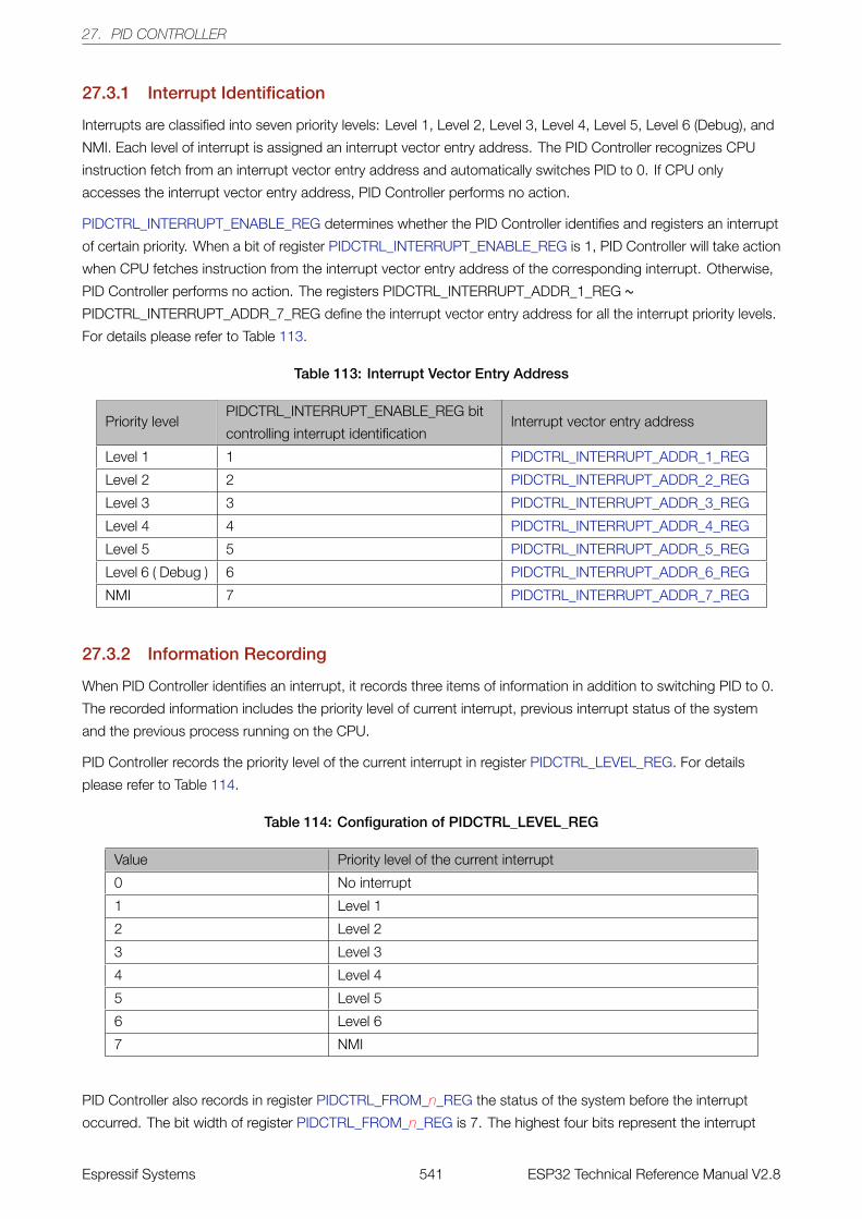
27. PID CONTROLLER
27.3.1 Interrupt Identification
Interrupts are classified into seven priority levels: Level 1, Level 2, Level 3, Level 4, Level 5, Level 6 (Debug), and
NMI. Each level of interrupt is assigned an interrupt vector entry address. The PID Controller recognizes CPU
instruction fetch from an interrupt vector entry address and automatically switches PID to 0. If CPU only
accesses the interrupt vector entry address, PID Controller performs no action.
PIDCTRL_INTERRUPT_ENABLE_REG determines whether the PID Controller identifies and registers an interrupt
of certain priority. When a bit of register PIDCTRL_INTERRUPT_ENABLE_REG is 1, PID Controller will take action
when CPU fetches instruction from the interrupt vector entry address of the corresponding interrupt. Otherwise,
PID Controller performs no action. The registers PIDCTRL_INTERRUPT_ADDR_1_REG ~PIDCTRL_INTERRUPT_ADDR_7_REG define the interrupt vector entry address for all the interrupt priority levels.
For details please refer to Table 113.
Table 113: Interrupt Vector Entry Address
Priority levelPIDCTRL_INTERRUPT_ENABLE_REG bit
controlling interrupt identificationInterrupt vector entry address
Level 1 1 PIDCTRL_INTERRUPT_ADDR_1_REG
Level 2 2 PIDCTRL_INTERRUPT_ADDR_2_REG
Level 3 3 PIDCTRL_INTERRUPT_ADDR_3_REG
Level 4 4 PIDCTRL_INTERRUPT_ADDR_4_REG
Level 5 5 PIDCTRL_INTERRUPT_ADDR_5_REG
Level 6 ( Debug ) 6 PIDCTRL_INTERRUPT_ADDR_6_REG
NMI 7 PIDCTRL_INTERRUPT_ADDR_7_REG
27.3.2 Information Recording
When PID Controller identifies an interrupt, it records three items of information in addition to switching PID to 0.
The recorded information includes the priority level of current interrupt, previous interrupt status of the system
and the previous process running on the CPU.
PID Controller records the priority level of the current interrupt in register PIDCTRL_LEVEL_REG. For details
please refer to Table 114.
Table 114: Configuration of PIDCTRL_LEVEL_REG
Value Priority level of the current interrupt
0 No interrupt
1 Level 1
2 Level 2
3 Level 3
4 Level 4
5 Level 5
6 Level 6
7 NMI
PID Controller also records in register PIDCTRL_FROM_n_REG the status of the system before the interrupt
occurred. The bit width of register PIDCTRL_FROM_n_REG is 7. The highest four bits represent the interrupt
Espressif Systems 541 ESP32 Technical Reference Manual V2.8
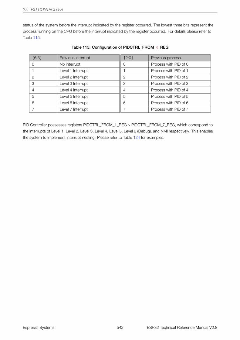
27. PID CONTROLLER
status of the system before the interrupt indicated by the register occurred. The lowest three bits represent the
process running on the CPU before the interrupt indicated by the register occurred. For details please refer to
Table 115.
Table 115: Configuration of PIDCTRL_FROM_n_REG
[6:3] Previous interrupt
0 No interrupt
1 Level 1 Interrupt
2 Level 2 Interrupt
3 Level 3 Interrupt
4 Level 4 Interrupt
5 Level 5 Interrupt
6 Level 6 Interrupt
7 Level 7 Interrupt
[2:0] Previous process
0 Process with PID of 0
1 Process with PID of 1
2 Process with PID of 2
3 Process with PID of 3
4 Process with PID of 4
5 Process with PID of 5
6 Process with PID of 6
7 Process with PID of 7
PID Controller possesses registers PIDCTRL_FROM_1_REG ~ PIDCTRL_FROM_7_REG, which correspond to
the interrupts of Level 1, Level 2, Level 3, Level 4, Level 5, Level 6 (Debug), and NMI respectively. This enables
the system to implement interrupt nesting. Please refer to Table 124 for examples.
Espressif Systems 542 ESP32 Technical Reference Manual V2.8
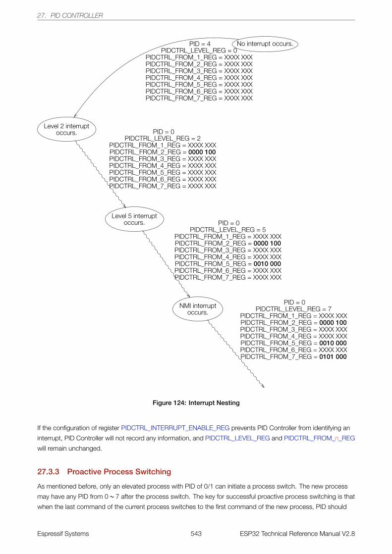
27. PID CONTROLLER
No interrupt occurs.PID = 4PIDCTRL_LEVEL_REG = 0
PIDCTRL_FROM_1_REG = XXXX XXXPIDCTRL_FROM_2_REG = XXXX XXXPIDCTRL_FROM_3_REG = XXXX XXXPIDCTRL_FROM_4_REG = XXXX XXXPIDCTRL_FROM_5_REG = XXXX XXXPIDCTRL_FROM_6_REG = XXXX XXXPIDCTRL_FROM_7_REG = XXXX XXX
��
Level 2 interruptoccurs. PID = 0
PIDCTRL_LEVEL_REG = 2PIDCTRL_FROM_1_REG = XXXX XXXPIDCTRL_FROM_2_REG = 0000 100PIDCTRL_FROM_3_REG = XXXX XXXPIDCTRL_FROM_4_REG = XXXX XXXPIDCTRL_FROM_5_REG = XXXX XXXPIDCTRL_FROM_6_REG = XXXX XXXPIDCTRL_FROM_7_REG = XXXX XXX
��
Level 5 interruptoccurs. PID = 0
PIDCTRL_LEVEL_REG = 5PIDCTRL_FROM_1_REG = XXXX XXXPIDCTRL_FROM_2_REG = 0000 100PIDCTRL_FROM_3_REG = XXXX XXXPIDCTRL_FROM_4_REG = XXXX XXXPIDCTRL_FROM_5_REG = 0010 000PIDCTRL_FROM_6_REG = XXXX XXXPIDCTRL_FROM_7_REG = XXXX XXX
��
NMI interruptoccurs.
PID = 0PIDCTRL_LEVEL_REG = 7
PIDCTRL_FROM_1_REG = XXXX XXXPIDCTRL_FROM_2_REG = 0000 100PIDCTRL_FROM_3_REG = XXXX XXXPIDCTRL_FROM_4_REG = XXXX XXXPIDCTRL_FROM_5_REG = 0010 000PIDCTRL_FROM_6_REG = XXXX XXXPIDCTRL_FROM_7_REG = 0101 000
��
Figure 124: Interrupt Nesting
If the configuration of register PIDCTRL_INTERRUPT_ENABLE_REG prevents PID Controller from identifying an
interrupt, PID Controller will not record any information, and PIDCTRL_LEVEL_REG and PIDCTRL_FROM_n_REG
will remain unchanged.
27.3.3 Proactive Process Switching
As mentioned before, only an elevated process with PID of 0/1 can initiate a process switch. The new process
may have any PID from 0 ~ 7 after the process switch. The key for successful proactive process switching is that
when the last command of the current process switches to the first command of the new process, PID should
Espressif Systems 543 ESP32 Technical Reference Manual V2.8
27. PID CONTROLLER
switch from 0/1 to that of the new process.
The software procedure for proactive process switching is as follows:
1. Mask all the interrupts except NMI by using software.
2. Set register PIDCTRL_NMI_MASK_ENABLE_REG to 1 to generate a CPU NMI Interrupt Mask signal.
3. Configure registers PIDCTRL_PID_DELAY_REG and PIDCTRL_NMI_DELAY_REG.
4. Configure register PIDCTRL_PID_NEW_REG.
5. Configure register PIDCTRL_LEVEL_REG and PIDCTRL_FROM_n_REG.
6. Set register PIDCTRL_PID_CONFIRM_REG and register PIDCTRL_NMI_MASK_DISABLE_REG to 1.
7. Revoke the masking of all interrupts but NMI.
8. Switch to the new process and fetch instruction.
Though we can deal with interrupt nesting, an elevated process should not be interrupted during the process
switching, and therefore the interrupts have been masked in step 1 and step 2.
In step 3, the configured values of registers PIDCTRL_PID_DELAY_REG and PIDCTRL_NMI_DELAY_REG will
affect step 6.
In step 4, the configured value of register PIDCTRL_PID_NEW_REG will be the new PID after step 6.
If the system is currently in a nested interrupt and needs to revert to the previous interrupt, register
PIDCTRL_LEVEL_REG must be restored based on the information recorded in register PIDCTRL_FROM_n_REG
in step 5.
In step 6, after the values of register PIDCTRL_PID_CONFIRM_REG and register
PIDCTRL_NMI_MASK_DISABLE_REG are set to 1, PID Controller will not immediately switch PID to the value of
register PIDCTRL_PID_NEW_REG, nor disable CPU NMI Interrupt Mask signal at once. Instead, PID Controller
performs each task after a different number of clock cycles. The numbers of clock cycles are the values specified
in register PIDCTRL_PID_DELAY_REG and PIDCTRL_NMI_DELAY_REG respectively.
In step 7, other tasks can be implemented as well. To do this, the cost of those tasks should be included when
configuring registers PIDCTRL_PID_DELAY_REG and PIDCTRL_NMI_DELAY_REG in step 3.
Espressif Systems 544 ESP32 Technical Reference Manual V2.8
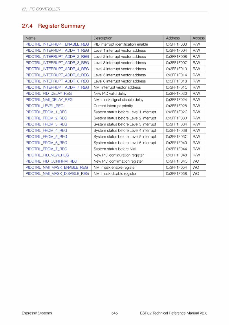
27. PID CONTROLLER
27.4 Register Summary
Name Description Address Access
PIDCTRL_INTERRUPT_ENABLE_REG PID interrupt identification enable 0x3FF1F000 R/W
PIDCTRL_INTERRUPT_ADDR_1_REG Level 1 interrupt vector address 0x3FF1F004 R/W
PIDCTRL_INTERRUPT_ADDR_2_REG Level 2 interrupt vector address 0x3FF1F008 R/W
PIDCTRL_INTERRUPT_ADDR_3_REG Level 3 interrupt vector address 0x3FF1F00C R/W
PIDCTRL_INTERRUPT_ADDR_4_REG Level 4 interrupt vector address 0x3FF1F010 R/W
PIDCTRL_INTERRUPT_ADDR_5_REG Level 5 interrupt vector address 0x3FF1F014 R/W
PIDCTRL_INTERRUPT_ADDR_6_REG Level 6 interrupt vector address 0x3FF1F018 R/W
PIDCTRL_INTERRUPT_ADDR_7_REG NMI interrupt vector address 0x3FF1F01C R/W
PIDCTRL_PID_DELAY_REG New PID valid delay 0x3FF1F020 R/W
PIDCTRL_NMI_DELAY_REG NMI mask signal disable delay 0x3FF1F024 R/W
PIDCTRL_LEVEL_REG Current interrupt priority 0x3FF1F028 R/W
PIDCTRL_FROM_1_REG System status before Level 1 interrupt 0x3FF1F02C R/W
PIDCTRL_FROM_2_REG System status before Level 2 interrupt 0x3FF1F030 R/W
PIDCTRL_FROM_3_REG System status before Level 3 interrupt 0x3FF1F034 R/W
PIDCTRL_FROM_4_REG System status before Level 4 interrupt 0x3FF1F038 R/W
PIDCTRL_FROM_5_REG System status before Level 5 interrupt 0x3FF1F03C R/W
PIDCTRL_FROM_6_REG System status before Level 6 interrupt 0x3FF1F040 R/W
PIDCTRL_FROM_7_REG System status before NMI 0x3FF1F044 R/W
PIDCTRL_PID_NEW_REG New PID configuration register 0x3FF1F048 R/W
PIDCTRL_PID_CONFIRM_REG New PID confirmation register 0x3FF1F04C WO
PIDCTRL_NMI_MASK_ENABLE_REG NMI mask enable register 0x3FF1F054 WO
PIDCTRL_NMI_MASK_DISABLE_REG NMI mask disable register 0x3FF1F058 WO
Espressif Systems 545 ESP32 Technical Reference Manual V2.8
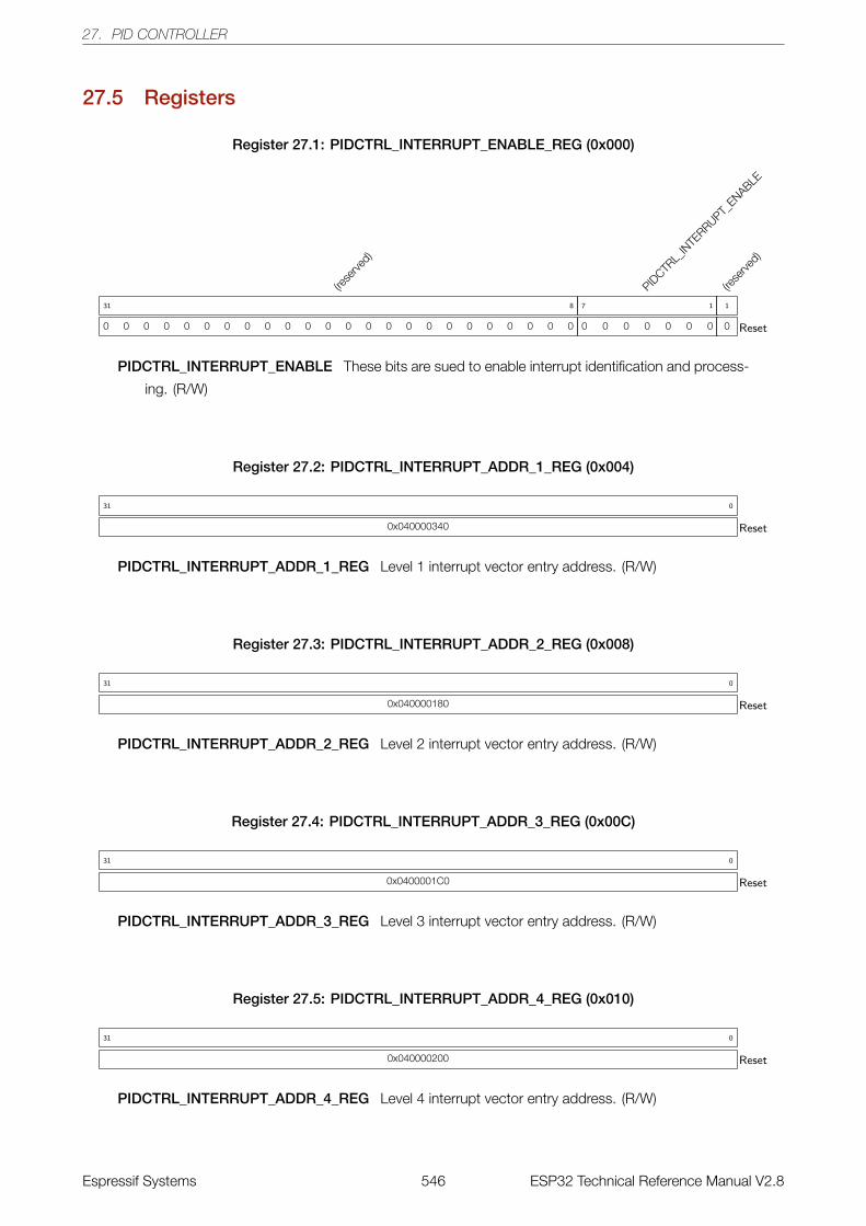
27. PID CONTROLLER
27.5 Registers
Register 27.1: PIDCTRL_INTERRUPT_ENABLE_REG (0x000)
(rese
rved)
0 0 0 0 0 0 0 0 0 0 0 0 0 0 0 0 0 0 0 0 0 0 0 0
31 8
PIDCTR
L_IN
TERRUPT_
ENABLE
0 0 0 0 0 0 0
7 1
(rese
rved)
0
1
Reset
PIDCTRL_INTERRUPT_ENABLE These bits are sued to enable interrupt identification and process-
ing. (R/W)
Register 27.2: PIDCTRL_INTERRUPT_ADDR_1_REG (0x004)
0x040000340
31 0
Reset
PIDCTRL_INTERRUPT_ADDR_1_REG Level 1 interrupt vector entry address. (R/W)
Register 27.3: PIDCTRL_INTERRUPT_ADDR_2_REG (0x008)
0x040000180
31 0
Reset
PIDCTRL_INTERRUPT_ADDR_2_REG Level 2 interrupt vector entry address. (R/W)
Register 27.4: PIDCTRL_INTERRUPT_ADDR_3_REG (0x00C)
0x0400001C0
31 0
Reset
PIDCTRL_INTERRUPT_ADDR_3_REG Level 3 interrupt vector entry address. (R/W)
Register 27.5: PIDCTRL_INTERRUPT_ADDR_4_REG (0x010)
0x040000200
31 0
Reset
PIDCTRL_INTERRUPT_ADDR_4_REG Level 4 interrupt vector entry address. (R/W)
Espressif Systems 546 ESP32 Technical Reference Manual V2.8
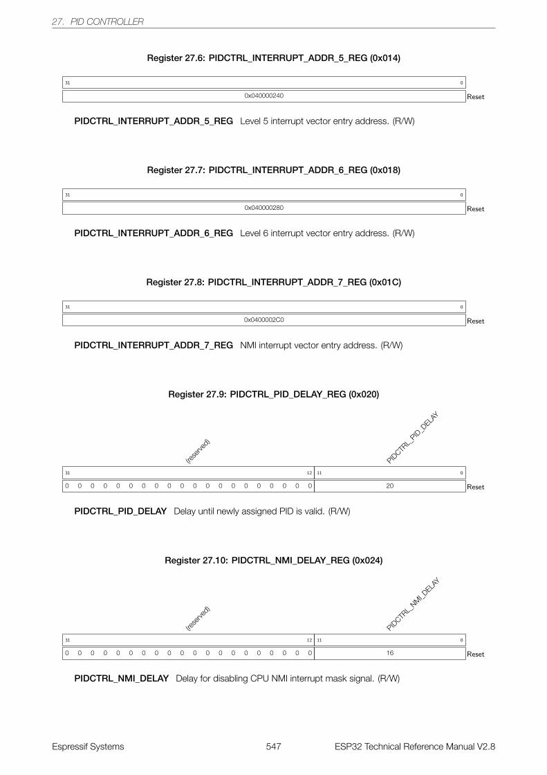
27. PID CONTROLLER
Register 27.6: PIDCTRL_INTERRUPT_ADDR_5_REG (0x014)
0x040000240
31 0
Reset
PIDCTRL_INTERRUPT_ADDR_5_REG Level 5 interrupt vector entry address. (R/W)
Register 27.7: PIDCTRL_INTERRUPT_ADDR_6_REG (0x018)
0x040000280
31 0
Reset
PIDCTRL_INTERRUPT_ADDR_6_REG Level 6 interrupt vector entry address. (R/W)
Register 27.8: PIDCTRL_INTERRUPT_ADDR_7_REG (0x01C)
0x0400002C0
31 0
Reset
PIDCTRL_INTERRUPT_ADDR_7_REG NMI interrupt vector entry address. (R/W)
Register 27.9: PIDCTRL_PID_DELAY_REG (0x020)
(rese
rved)
0 0 0 0 0 0 0 0 0 0 0 0 0 0 0 0 0 0 0 0
31 12
PIDCTR
L_PID
_DELA
Y
20
11 0
Reset
PIDCTRL_PID_DELAY Delay until newly assigned PID is valid. (R/W)
Register 27.10: PIDCTRL_NMI_DELAY_REG (0x024)
(rese
rved)
0 0 0 0 0 0 0 0 0 0 0 0 0 0 0 0 0 0 0 0
31 12
PIDCTR
L_NM
I_DELA
Y
16
11 0
Reset
PIDCTRL_NMI_DELAY Delay for disabling CPU NMI interrupt mask signal. (R/W)
Espressif Systems 547 ESP32 Technical Reference Manual V2.8
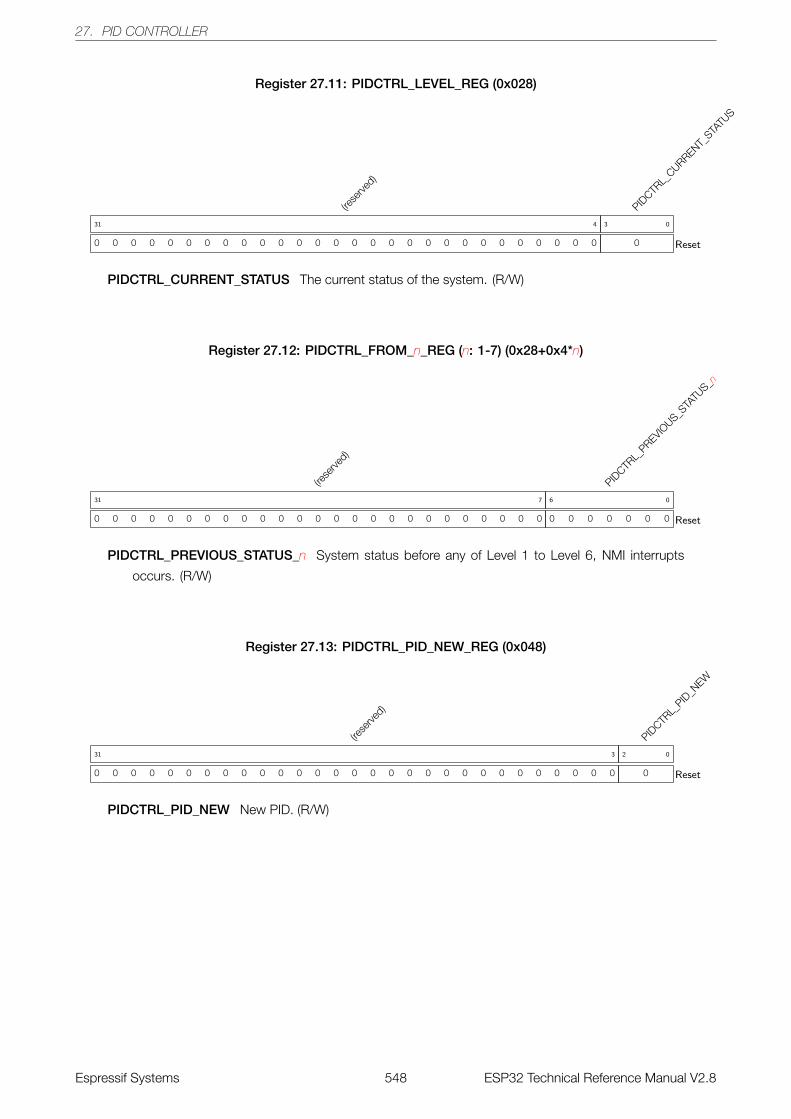
27. PID CONTROLLER
Register 27.11: PIDCTRL_LEVEL_REG (0x028)
(rese
rved)
0 0 0 0 0 0 0 0 0 0 0 0 0 0 0 0 0 0 0 0 0 0 0 0 0 0 0 0
31 4
PIDCTR
L_CURRENT_
STATU
S
0
3 0
Reset
PIDCTRL_CURRENT_STATUS The current status of the system. (R/W)
Register 27.12: PIDCTRL_FROM_n_REG (n: 1-7) (0x28+0x4*n)
(rese
rved)
0 0 0 0 0 0 0 0 0 0 0 0 0 0 0 0 0 0 0 0 0 0 0 0 0
31 7
PIDCTR
L_PREVIO
US_STA
TUS_n
0 0 0 0 0 0 0
6 0
Reset
PIDCTRL_PREVIOUS_STATUS_n System status before any of Level 1 to Level 6, NMI interrupts
occurs. (R/W)
Register 27.13: PIDCTRL_PID_NEW_REG (0x048)
(rese
rved)
0 0 0 0 0 0 0 0 0 0 0 0 0 0 0 0 0 0 0 0 0 0 0 0 0 0 0 0 0
31 3
PIDCTR
L_PID
_NEW
0
2 0
Reset
PIDCTRL_PID_NEW New PID. (R/W)
Espressif Systems 548 ESP32 Technical Reference Manual V2.8
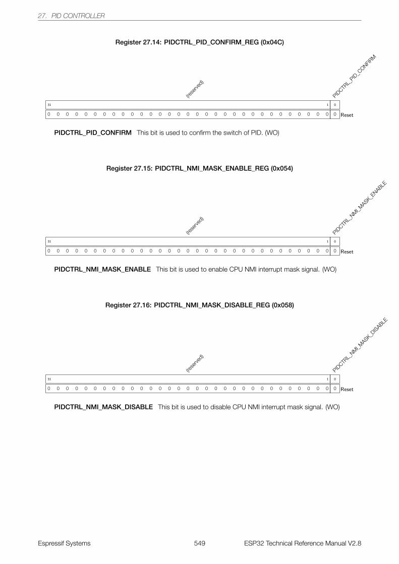
27. PID CONTROLLER
Register 27.14: PIDCTRL_PID_CONFIRM_REG (0x04C)
(rese
rved)
0 0 0 0 0 0 0 0 0 0 0 0 0 0 0 0 0 0 0 0 0 0 0 0 0 0 0 0 0 0 0
31 1
PIDCTR
L_PID
_CONFIR
M
0
0
Reset
PIDCTRL_PID_CONFIRM This bit is used to confirm the switch of PID. (WO)
Register 27.15: PIDCTRL_NMI_MASK_ENABLE_REG (0x054)
(rese
rved)
0 0 0 0 0 0 0 0 0 0 0 0 0 0 0 0 0 0 0 0 0 0 0 0 0 0 0 0 0 0 0
31 1
PIDCTR
L_NM
I_MASK_E
NABLE
0
0
Reset
PIDCTRL_NMI_MASK_ENABLE This bit is used to enable CPU NMI interrupt mask signal. (WO)
Register 27.16: PIDCTRL_NMI_MASK_DISABLE_REG (0x058)
(rese
rved)
0 0 0 0 0 0 0 0 0 0 0 0 0 0 0 0 0 0 0 0 0 0 0 0 0 0 0 0 0 0 0
31 1
PIDCTR
L_NM
I_MASK_D
ISABLE
0
0
Reset
PIDCTRL_NMI_MASK_DISABLE This bit is used to disable CPU NMI interrupt mask signal. (WO)
Espressif Systems 549 ESP32 Technical Reference Manual V2.8
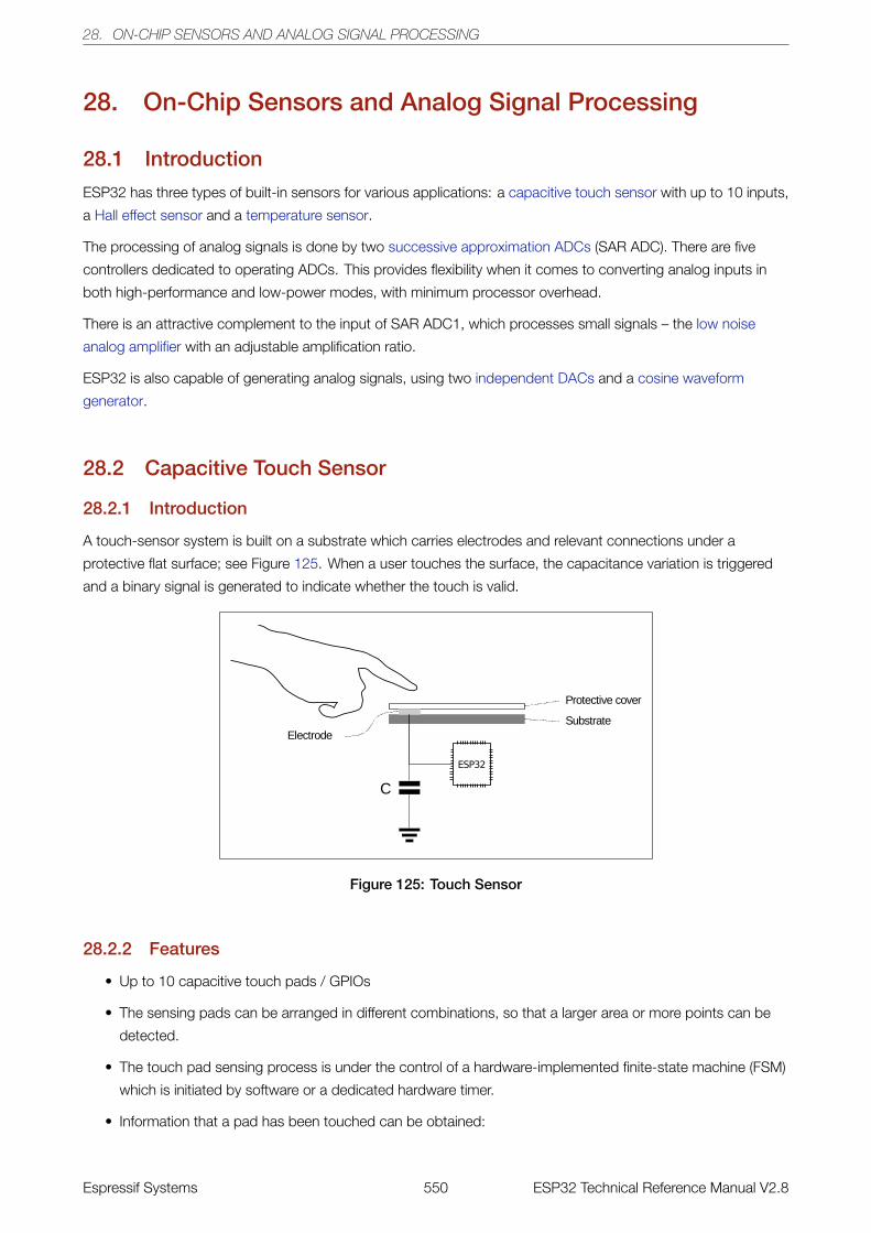
28. ON-CHIP SENSORS AND ANALOG SIGNAL PROCESSING
28. On-Chip Sensors and Analog Signal Processing
28.1 Introduction
ESP32 has three types of built-in sensors for various applications: a capacitive touch sensor with up to 10 inputs,
a Hall effect sensor and a temperature sensor.
The processing of analog signals is done by two successive approximation ADCs (SAR ADC). There are five
controllers dedicated to operating ADCs. This provides flexibility when it comes to converting analog inputs in
both high-performance and low-power modes, with minimum processor overhead.
There is an attractive complement to the input of SAR ADC1, which processes small signals – the low noise
analog amplifier with an adjustable amplification ratio.
ESP32 is also capable of generating analog signals, using two independent DACs and a cosine waveform
generator.
28.2 Capacitive Touch Sensor
28.2.1 Introduction
A touch-sensor system is built on a substrate which carries electrodes and relevant connections under a
protective flat surface; see Figure 125. When a user touches the surface, the capacitance variation is triggered
and a binary signal is generated to indicate whether the touch is valid.
Figure 125: Touch Sensor
28.2.2 Features
• Up to 10 capacitive touch pads / GPIOs
• The sensing pads can be arranged in different combinations, so that a larger area or more points can be
detected.
• The touch pad sensing process is under the control of a hardware-implemented finite-state machine (FSM)
which is initiated by software or a dedicated hardware timer.
• Information that a pad has been touched can be obtained:
Espressif Systems 550 ESP32 Technical Reference Manual V2.8
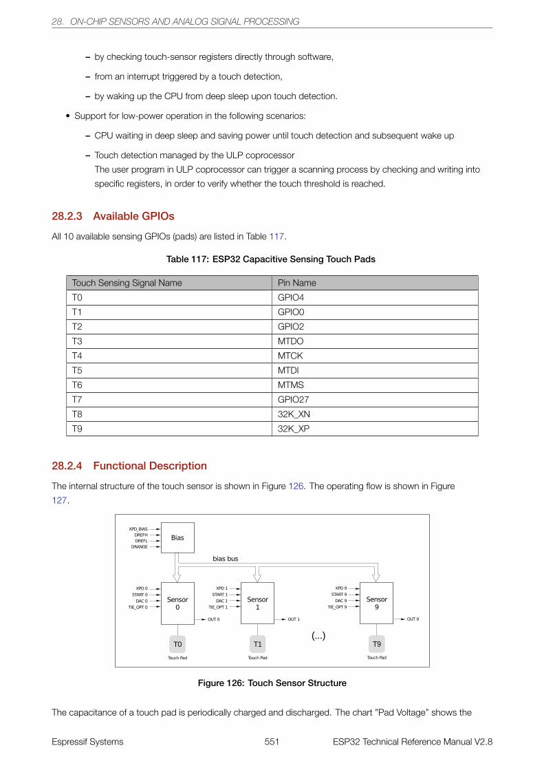
28. ON-CHIP SENSORS AND ANALOG SIGNAL PROCESSING
– by checking touch-sensor registers directly through software,
– from an interrupt triggered by a touch detection,
– by waking up the CPU from deep sleep upon touch detection.
• Support for low-power operation in the following scenarios:
– CPU waiting in deep sleep and saving power until touch detection and subsequent wake up
– Touch detection managed by the ULP coprocessor
The user program in ULP coprocessor can trigger a scanning process by checking and writing into
specific registers, in order to verify whether the touch threshold is reached.
28.2.3 Available GPIOs
All 10 available sensing GPIOs (pads) are listed in Table 117.
Table 117: ESP32 Capacitive Sensing Touch Pads
Touch Sensing Signal Name Pin Name
T0 GPIO4
T1 GPIO0
T2 GPIO2
T3 MTDO
T4 MTCK
T5 MTDI
T6 MTMS
T7 GPIO27
T8 32K_XN
T9 32K_XP
28.2.4 Functional Description
The internal structure of the touch sensor is shown in Figure 126. The operating flow is shown in Figure
127.
Figure 126: Touch Sensor Structure
The capacitance of a touch pad is periodically charged and discharged. The chart ”Pad Voltage” shows the
Espressif Systems 551 ESP32 Technical Reference Manual V2.8
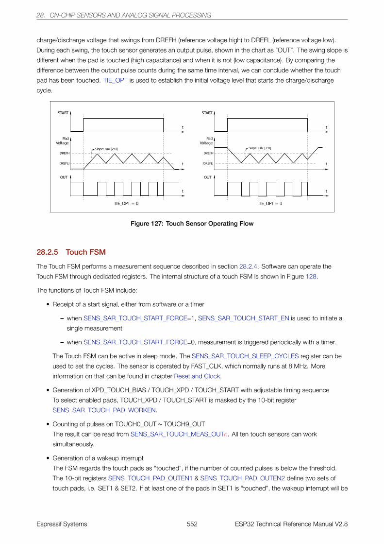
28. ON-CHIP SENSORS AND ANALOG SIGNAL PROCESSING
charge/discharge voltage that swings from DREFH (reference voltage high) to DREFL (reference voltage low).
During each swing, the touch sensor generates an output pulse, shown in the chart as ”OUT”. The swing slope is
different when the pad is touched (high capacitance) and when it is not (low capacitance). By comparing the
difference between the output pulse counts during the same time interval, we can conclude whether the touch
pad has been touched. TIE_OPT is used to establish the initial voltage level that starts the charge/discharge
cycle.
Figure 127: Touch Sensor Operating Flow
28.2.5 Touch FSM
The Touch FSM performs a measurement sequence described in section 28.2.4. Software can operate the
Touch FSM through dedicated registers. The internal structure of a touch FSM is shown in Figure 128.
The functions of Touch FSM include:
• Receipt of a start signal, either from software or a timer
– when SENS_SAR_TOUCH_START_FORCE=1, SENS_SAR_TOUCH_START_EN is used to initiate a
single measurement
– when SENS_SAR_TOUCH_START_FORCE=0, measurement is triggered periodically with a timer.
The Touch FSM can be active in sleep mode. The SENS_SAR_TOUCH_SLEEP_CYCLES register can be
used to set the cycles. The sensor is operated by FAST_CLK, which normally runs at 8 MHz. More
information on that can be found in chapter Reset and Clock.
• Generation of XPD_TOUCH_BIAS / TOUCH_XPD / TOUCH_START with adjustable timing sequence
To select enabled pads, TOUCH_XPD / TOUCH_START is masked by the 10-bit register
SENS_SAR_TOUCH_PAD_WORKEN.
• Counting of pulses on TOUCH0_OUT ~ TOUCH9_OUT
The result can be read from SENS_SAR_TOUCH_MEAS_OUTn. All ten touch sensors can work
simultaneously.
• Generation of a wakeup interrupt
The FSM regards the touch pads as “touched”, if the number of counted pulses is below the threshold.
The 10-bit registers SENS_TOUCH_PAD_OUTEN1 & SENS_TOUCH_PAD_OUTEN2 define two sets of
touch pads, i.e. SET1 & SET2. If at least one of the pads in SET1 is “touched”, the wakeup interrupt will be
Espressif Systems 552 ESP32 Technical Reference Manual V2.8
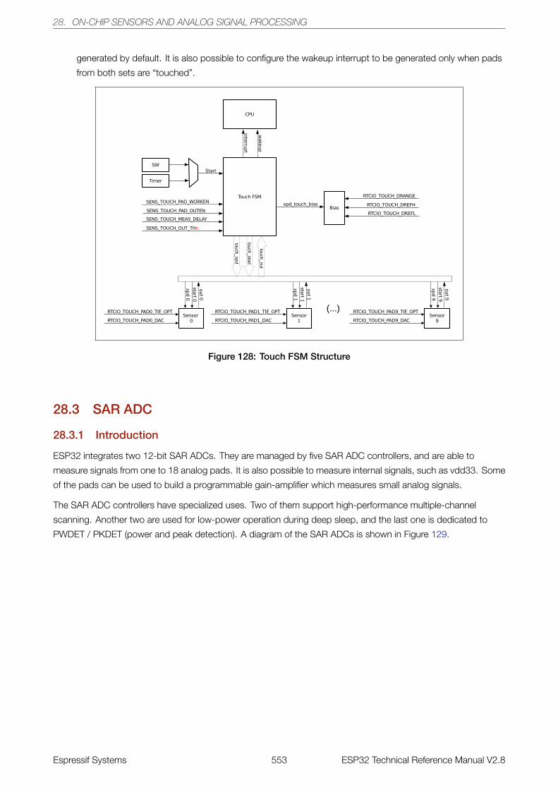
28. ON-CHIP SENSORS AND ANALOG SIGNAL PROCESSING
generated by default. It is also possible to configure the wakeup interrupt to be generated only when pads
from both sets are “touched”.
Figure 128: Touch FSM Structure
28.3 SAR ADC
28.3.1 Introduction
ESP32 integrates two 12-bit SAR ADCs. They are managed by five SAR ADC controllers, and are able to
measure signals from one to 18 analog pads. It is also possible to measure internal signals, such as vdd33. Some
of the pads can be used to build a programmable gain-amplifier which measures small analog signals.
The SAR ADC controllers have specialized uses. Two of them support high-performance multiple-channel
scanning. Another two are used for low-power operation during deep sleep, and the last one is dedicated to
PWDET / PKDET (power and peak detection). A diagram of the SAR ADCs is shown in Figure 129.
Espressif Systems 553 ESP32 Technical Reference Manual V2.8
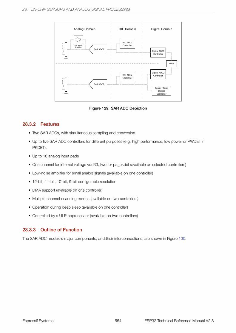
28. ON-CHIP SENSORS AND ANALOG SIGNAL PROCESSING
Figure 129: SAR ADC Depiction
28.3.2 Features
• Two SAR ADCs, with simultaneous sampling and conversion
• Up to five SAR ADC controllers for different purposes (e.g. high performance, low power or PWDET /
PKDET).
• Up to 18 analog input pads
• One channel for internal voltage vdd33, two for pa_pkdet (available on selected controllers)
• Low-noise amplifier for small analog signals (available on one controller)
• 12-bit, 11-bit, 10-bit, 9-bit configurable resolution
• DMA support (available on one controller)
• Multiple channel-scanning modes (available on two controllers)
• Operation during deep sleep (available on one controller)
• Controlled by a ULP coprocessor (available on two controllers)
28.3.3 Outline of Function
The SAR ADC module’s major components, and their interconnections, are shown in Figure 130.
Espressif Systems 554 ESP32 Technical Reference Manual V2.8
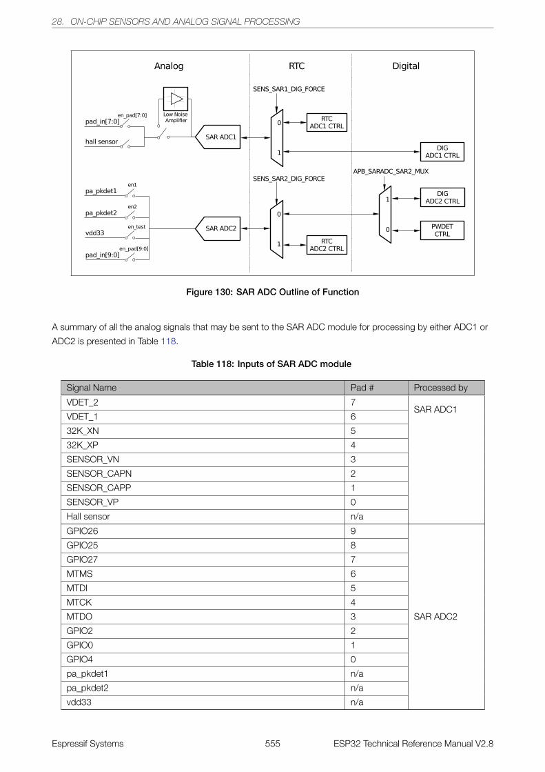
28. ON-CHIP SENSORS AND ANALOG SIGNAL PROCESSING
Figure 130: SAR ADC Outline of Function
A summary of all the analog signals that may be sent to the SAR ADC module for processing by either ADC1 or
ADC2 is presented in Table 118.
Table 118: Inputs of SAR ADC module
Signal Name Pad # Processed by
VDET_2 7SAR ADC1
VDET_1 6
32K_XN 5
32K_XP 4
SENSOR_VN 3
SENSOR_CAPN 2
SENSOR_CAPP 1
SENSOR_VP 0
Hall sensor n/a
GPIO26 9
SAR ADC2
GPIO25 8
GPIO27 7
MTMS 6
MTDI 5
MTCK 4
MTDO 3
GPIO2 2
GPIO0 1
GPIO4 0
pa_pkdet1 n/a
pa_pkdet2 n/a
vdd33 n/a
Espressif Systems 555 ESP32 Technical Reference Manual V2.8
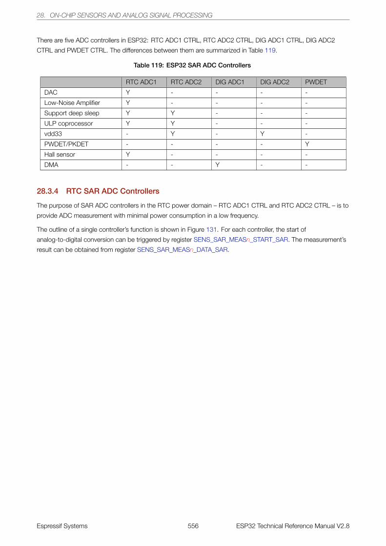
28. ON-CHIP SENSORS AND ANALOG SIGNAL PROCESSING
There are five ADC controllers in ESP32: RTC ADC1 CTRL, RTC ADC2 CTRL, DIG ADC1 CTRL, DIG ADC2
CTRL and PWDET CTRL. The differences between them are summarized in Table 119.
Table 119: ESP32 SAR ADC Controllers
RTC ADC1 RTC ADC2 DIG ADC1 DIG ADC2 PWDET
DAC Y - - - -
Low-Noise Amplifier Y - - - -
Support deep sleep Y Y - - -
ULP coprocessor Y Y - - -
vdd33 - Y - Y -
PWDET/PKDET - - - - Y
Hall sensor Y - - - -
DMA - - Y - -
28.3.4 RTC SAR ADC Controllers
The purpose of SAR ADC controllers in the RTC power domain – RTC ADC1 CTRL and RTC ADC2 CTRL – is to
provide ADC measurement with minimal power consumption in a low frequency.
The outline of a single controller’s function is shown in Figure 131. For each controller, the start of
analog-to-digital conversion can be triggered by register SENS_SAR_MEASn_START_SAR. The measurement’s
result can be obtained from register SENS_SAR_MEASn_DATA_SAR.
Espressif Systems 556 ESP32 Technical Reference Manual V2.8
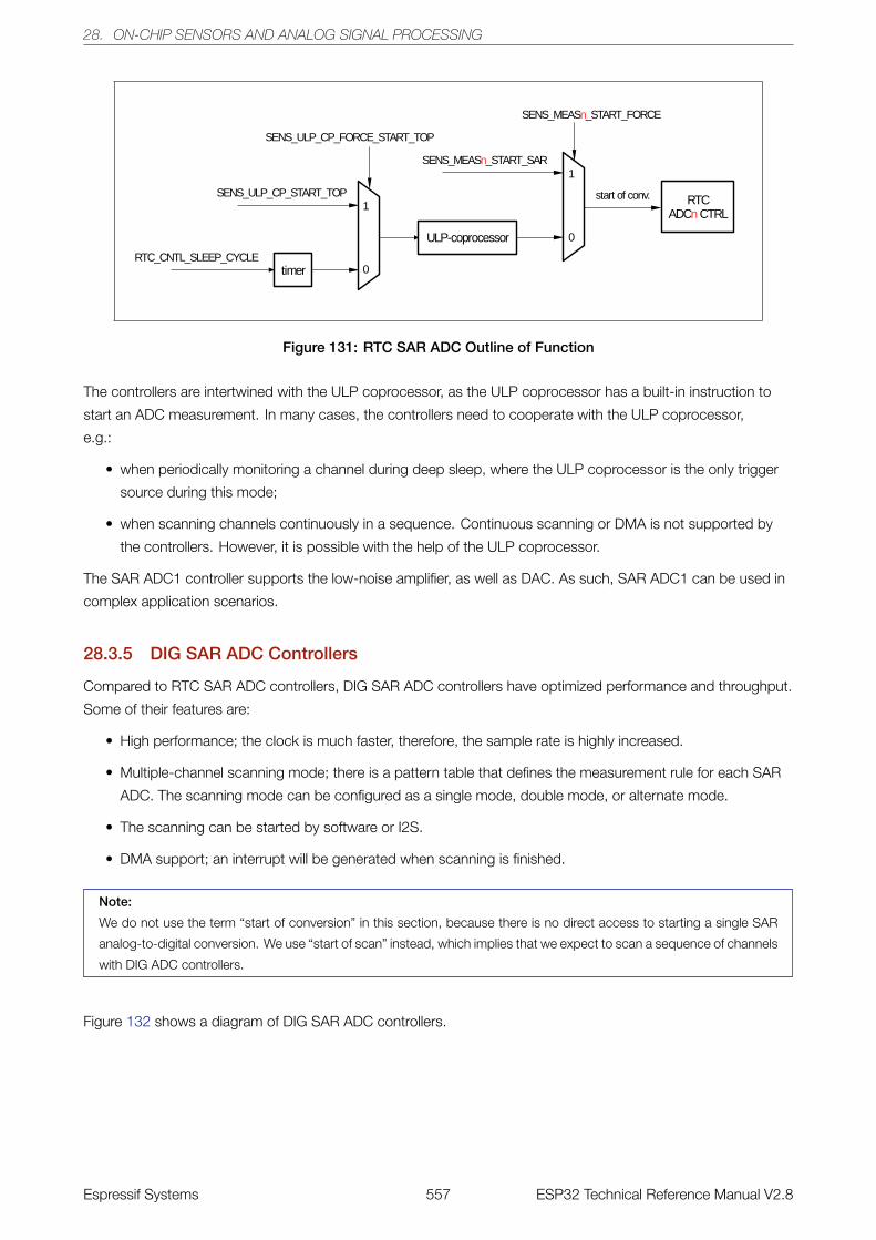
28. ON-CHIP SENSORS AND ANALOG SIGNAL PROCESSING
Figure 131: RTC SAR ADC Outline of Function
The controllers are intertwined with the ULP coprocessor, as the ULP coprocessor has a built-in instruction to
start an ADC measurement. In many cases, the controllers need to cooperate with the ULP coprocessor,
e.g.:
• when periodically monitoring a channel during deep sleep, where the ULP coprocessor is the only trigger
source during this mode;
• when scanning channels continuously in a sequence. Continuous scanning or DMA is not supported by
the controllers. However, it is possible with the help of the ULP coprocessor.
The SAR ADC1 controller supports the low-noise amplifier, as well as DAC. As such, SAR ADC1 can be used in
complex application scenarios.
28.3.5 DIG SAR ADC Controllers
Compared to RTC SAR ADC controllers, DIG SAR ADC controllers have optimized performance and throughput.
Some of their features are:
• High performance; the clock is much faster, therefore, the sample rate is highly increased.
• Multiple-channel scanning mode; there is a pattern table that defines the measurement rule for each SAR
ADC. The scanning mode can be configured as a single mode, double mode, or alternate mode.
• The scanning can be started by software or I2S.
• DMA support; an interrupt will be generated when scanning is finished.
Note:
We do not use the term “start of conversion” in this section, because there is no direct access to starting a single SAR
analog-to-digital conversion. We use “start of scan” instead, which implies that we expect to scan a sequence of channels
with DIG ADC controllers.
Figure 132 shows a diagram of DIG SAR ADC controllers.
Espressif Systems 557 ESP32 Technical Reference Manual V2.8
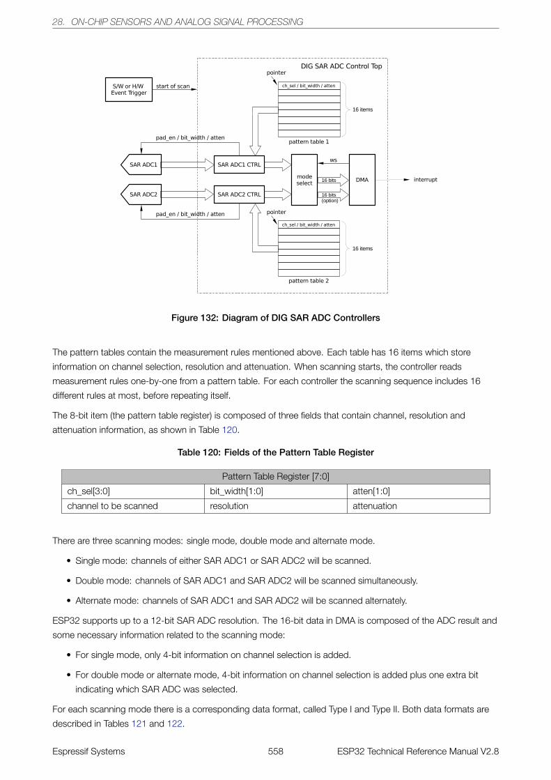
28. ON-CHIP SENSORS AND ANALOG SIGNAL PROCESSING
Figure 132: Diagram of DIG SAR ADC Controllers
The pattern tables contain the measurement rules mentioned above. Each table has 16 items which store
information on channel selection, resolution and attenuation. When scanning starts, the controller reads
measurement rules one-by-one from a pattern table. For each controller the scanning sequence includes 16
different rules at most, before repeating itself.
The 8-bit item (the pattern table register) is composed of three fields that contain channel, resolution and
attenuation information, as shown in Table 120.
Table 120: Fields of the Pattern Table Register
Pattern Table Register [7:0]
ch_sel[3:0] bit_width[1:0] atten[1:0]
channel to be scanned resolution attenuation
There are three scanning modes: single mode, double mode and alternate mode.
• Single mode: channels of either SAR ADC1 or SAR ADC2 will be scanned.
• Double mode: channels of SAR ADC1 and SAR ADC2 will be scanned simultaneously.
• Alternate mode: channels of SAR ADC1 and SAR ADC2 will be scanned alternately.
ESP32 supports up to a 12-bit SAR ADC resolution. The 16-bit data in DMA is composed of the ADC result and
some necessary information related to the scanning mode:
• For single mode, only 4-bit information on channel selection is added.
• For double mode or alternate mode, 4-bit information on channel selection is added plus one extra bit
indicating which SAR ADC was selected.
For each scanning mode there is a corresponding data format, called Type I and Type II. Both data formats are
described in Tables 121 and 122.
Espressif Systems 558 ESP32 Technical Reference Manual V2.8
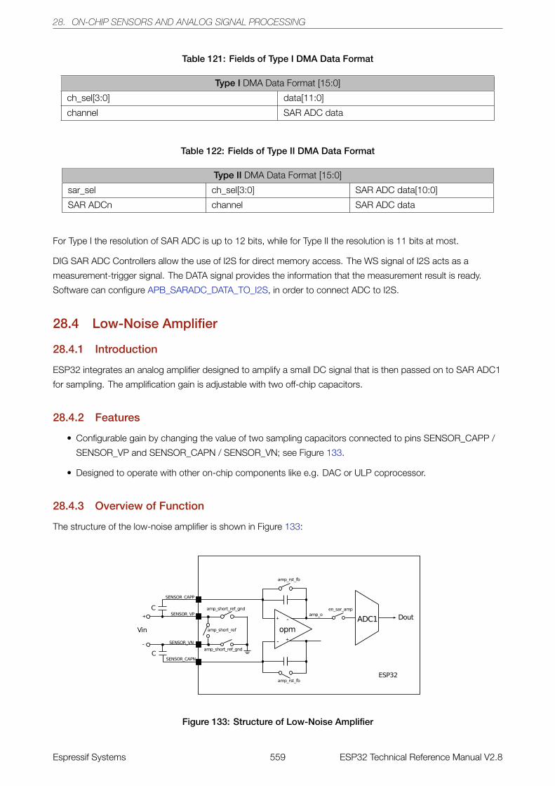
28. ON-CHIP SENSORS AND ANALOG SIGNAL PROCESSING
Table 121: Fields of Type I DMA Data Format
Type I DMA Data Format [15:0]
ch_sel[3:0] data[11:0]
channel SAR ADC data
Table 122: Fields of Type II DMA Data Format
Type II DMA Data Format [15:0]
sar_sel ch_sel[3:0] SAR ADC data[10:0]
SAR ADCn channel SAR ADC data
For Type I the resolution of SAR ADC is up to 12 bits, while for Type II the resolution is 11 bits at most.
DIG SAR ADC Controllers allow the use of I2S for direct memory access. The WS signal of I2S acts as a
measurement-trigger signal. The DATA signal provides the information that the measurement result is ready.
Software can configure APB_SARADC_DATA_TO_I2S, in order to connect ADC to I2S.
28.4 Low-Noise Amplifier
28.4.1 Introduction
ESP32 integrates an analog amplifier designed to amplify a small DC signal that is then passed on to SAR ADC1
for sampling. The amplification gain is adjustable with two off-chip capacitors.
28.4.2 Features
• Configurable gain by changing the value of two sampling capacitors connected to pins SENSOR_CAPP /
SENSOR_VP and SENSOR_CAPN / SENSOR_VN; see Figure 133.
• Designed to operate with other on-chip components like e.g. DAC or ULP coprocessor.
28.4.3 Overview of Function
The structure of the low-noise amplifier is shown in Figure 133:
Figure 133: Structure of Low-Noise Amplifier
Espressif Systems 559 ESP32 Technical Reference Manual V2.8
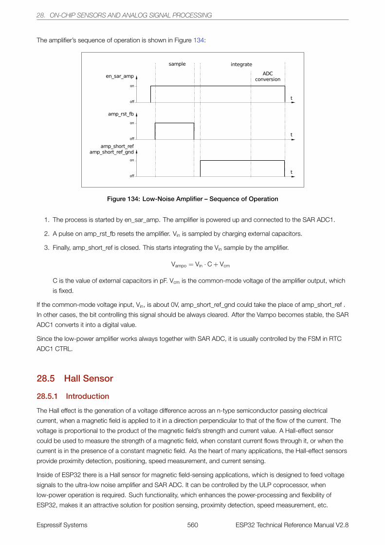
28. ON-CHIP SENSORS AND ANALOG SIGNAL PROCESSING
The amplifier’s sequence of operation is shown in Figure 134:
Figure 134: Low-Noise Amplifier – Sequence of Operation
1. The process is started by en_sar_amp. The amplifier is powered up and connected to the SAR ADC1.
2. A pulse on amp_rst_fb resets the amplifier. Vin is sampled by charging external capacitors.
3. Finally, amp_short_ref is closed. This starts integrating the Vin sample by the amplifier.
Vampo = Vin · C + Vcm
C is the value of external capacitors in pF. Vcm is the common-mode voltage of the amplifier output, which
is fixed.
If the common-mode voltage input, Vin, is about 0V, amp_short_ref_gnd could take the place of amp_short_ref .
In other cases, the bit controlling this signal should be always cleared. After the Vampo becomes stable, the SAR
ADC1 converts it into a digital value.
Since the low-power amplifier works always together with SAR ADC, it is usually controlled by the FSM in RTC
ADC1 CTRL.
28.5 Hall Sensor
28.5.1 Introduction
The Hall effect is the generation of a voltage difference across an n-type semiconductor passing electrical
current, when a magnetic field is applied to it in a direction perpendicular to that of the flow of the current. The
voltage is proportional to the product of the magnetic field’s strength and current value. A Hall-effect sensor
could be used to measure the strength of a magnetic field, when constant current flows through it, or when the
current is in the presence of a constant magnetic field. As the heart of many applications, the Hall-effect sensors
provide proximity detection, positioning, speed measurement, and current sensing.
Inside of ESP32 there is a Hall sensor for magnetic field-sensing applications, which is designed to feed voltage
signals to the ultra-low noise amplifier and SAR ADC. It can be controlled by the ULP coprocessor, when
low-power operation is required. Such functionality, which enhances the power-processing and flexibility of
ESP32, makes it an attractive solution for position sensing, proximity detection, speed measurement, etc.
Espressif Systems 560 ESP32 Technical Reference Manual V2.8
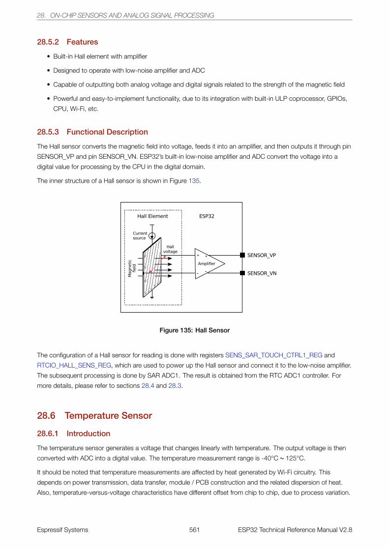
28. ON-CHIP SENSORS AND ANALOG SIGNAL PROCESSING
28.5.2 Features
• Built-in Hall element with amplifier
• Designed to operate with low-noise amplifier and ADC
• Capable of outputting both analog voltage and digital signals related to the strength of the magnetic field
• Powerful and easy-to-implement functionality, due to its integration with built-in ULP coprocessor, GPIOs,
CPU, Wi-Fi, etc.
28.5.3 Functional Description
The Hall sensor converts the magnetic field into voltage, feeds it into an amplifier, and then outputs it through pin
SENSOR_VP and pin SENSOR_VN. ESP32’s built-in low-noise amplifier and ADC convert the voltage into a
digital value for processing by the CPU in the digital domain.
The inner structure of a Hall sensor is shown in Figure 135.
Figure 135: Hall Sensor
The configuration of a Hall sensor for reading is done with registers SENS_SAR_TOUCH_CTRL1_REG and
RTCIO_HALL_SENS_REG, which are used to power up the Hall sensor and connect it to the low-noise amplifier.
The subsequent processing is done by SAR ADC1. The result is obtained from the RTC ADC1 controller. For
more details, please refer to sections 28.4 and 28.3.
28.6 Temperature Sensor
28.6.1 Introduction
The temperature sensor generates a voltage that changes linearly with temperature. The output voltage is then
converted with ADC into a digital value. The temperature measurement range is -40°C ~ 125°C.
It should be noted that temperature measurements are affected by heat generated by Wi-Fi circuitry. This
depends on power transmission, data transfer, module / PCB construction and the related dispersion of heat.
Also, temperature-versus-voltage characteristics have different offset from chip to chip, due to process variation.
Espressif Systems 561 ESP32 Technical Reference Manual V2.8
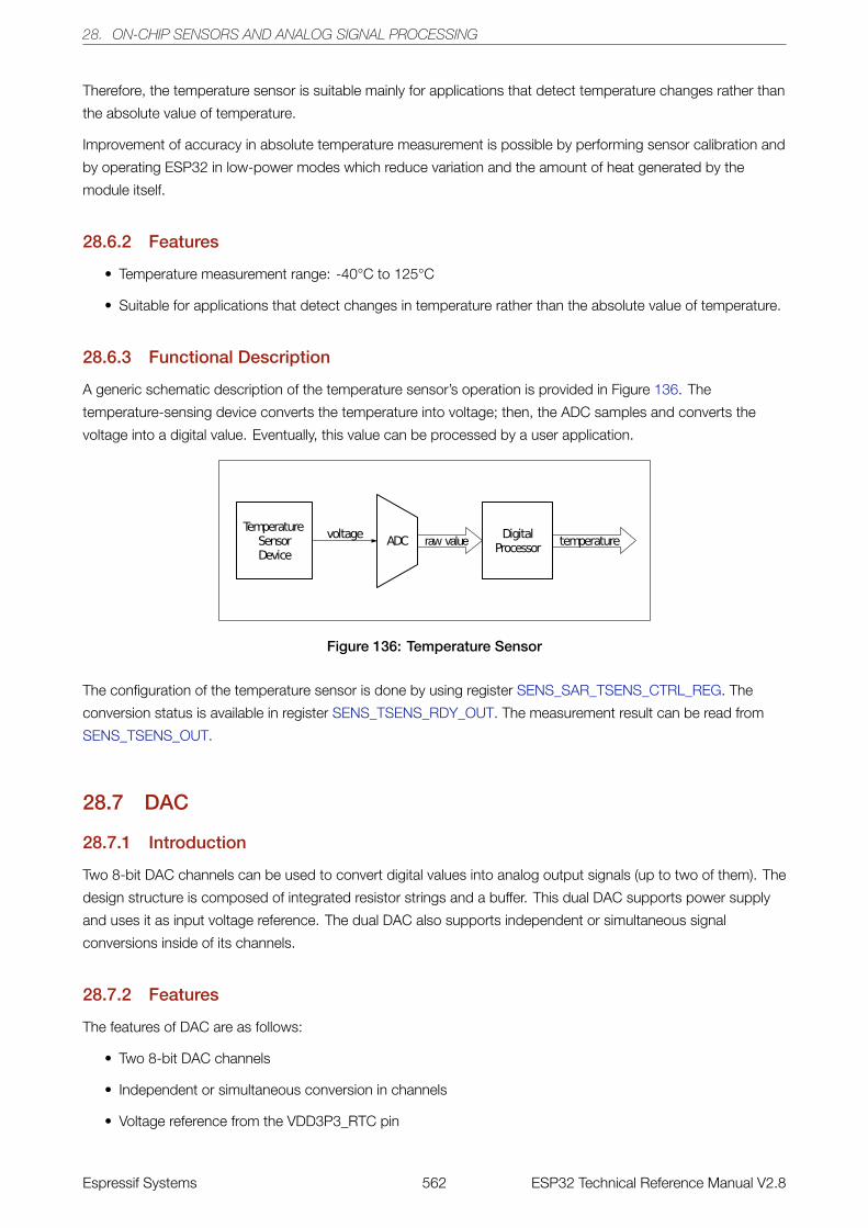
28. ON-CHIP SENSORS AND ANALOG SIGNAL PROCESSING
Therefore, the temperature sensor is suitable mainly for applications that detect temperature changes rather than
the absolute value of temperature.
Improvement of accuracy in absolute temperature measurement is possible by performing sensor calibration and
by operating ESP32 in low-power modes which reduce variation and the amount of heat generated by the
module itself.
28.6.2 Features
• Temperature measurement range: -40°C to 125°C
• Suitable for applications that detect changes in temperature rather than the absolute value of temperature.
28.6.3 Functional Description
A generic schematic description of the temperature sensor’s operation is provided in Figure 136. The
temperature-sensing device converts the temperature into voltage; then, the ADC samples and converts the
voltage into a digital value. Eventually, this value can be processed by a user application.
Figure 136: Temperature Sensor
The configuration of the temperature sensor is done by using register SENS_SAR_TSENS_CTRL_REG. The
conversion status is available in register SENS_TSENS_RDY_OUT. The measurement result can be read from
SENS_TSENS_OUT.
28.7 DAC
28.7.1 Introduction
Two 8-bit DAC channels can be used to convert digital values into analog output signals (up to two of them). The
design structure is composed of integrated resistor strings and a buffer. This dual DAC supports power supply
and uses it as input voltage reference. The dual DAC also supports independent or simultaneous signal
conversions inside of its channels.
28.7.2 Features
The features of DAC are as follows:
• Two 8-bit DAC channels
• Independent or simultaneous conversion in channels
• Voltage reference from the VDD3P3_RTC pin
Espressif Systems 562 ESP32 Technical Reference Manual V2.8
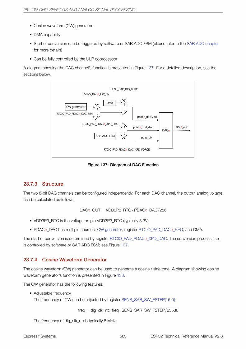
28. ON-CHIP SENSORS AND ANALOG SIGNAL PROCESSING
• Cosine waveform (CW) generator
• DMA capability
• Start of conversion can be triggered by software or SAR ADC FSM (please refer to the SAR ADC chapter
for more details)
• Can be fully controlled by the ULP coprocessor
A diagram showing the DAC channel’s function is presented in Figure 137. For a detailed description, see the
sections below.
Figure 137: Diagram of DAC Function
28.7.3 Structure
The two 8-bit DAC channels can be configured independently. For each DAC channel, the output analog voltage
can be calculated as follows:
DACn_OUT = VDD3P3_RTC · PDACn_DAC/256
• VDD3P3_RTC is the voltage on pin VDD3P3_RTC (typically 3.3V).
• PDACn_DAC has multiple sources: CW generator, register RTCIO_PAD_DACn_REG, and DMA.
The start of conversion is determined by register RTCIO_PAD_PDACn_XPD_DAC. The conversion process itself
is controlled by software or SAR ADC FSM; see Figure 137.
28.7.4 Cosine Waveform Generator
The cosine waveform (CW) generator can be used to generate a cosine / sine tone. A diagram showing cosine
waveform generator’s function is presented in Figure 138.
The CW generator has the following features:
• Adjustable frequency
The frequency of CW can be adjusted by register SENS_SAR_SW_FSTEP[15:0]:
freq = dig_clk_rtc_freq · SENS_SAR_SW_FSTEP/65536
The frequency of dig_clk_rtc is typically 8 MHz.
Espressif Systems 563 ESP32 Technical Reference Manual V2.8
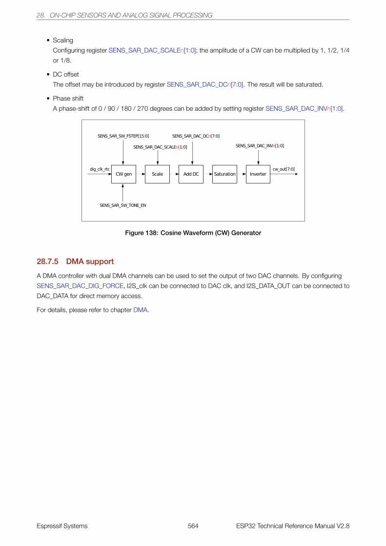
28. ON-CHIP SENSORS AND ANALOG SIGNAL PROCESSING
• Scaling
Configuring register SENS_SAR_DAC_SCALEn[1:0]; the amplitude of a CW can be multiplied by 1, 1/2, 1/4
or 1/8.
• DC offset
The offset may be introduced by register SENS_SAR_DAC_DCn[7:0]. The result will be saturated.
• Phase shift
A phase-shift of 0 / 90 / 180 / 270 degrees can be added by setting register SENS_SAR_DAC_INVn[1:0].
Figure 138: Cosine Waveform (CW) Generator
28.7.5 DMA support
A DMA controller with dual DMA channels can be used to set the output of two DAC channels. By configuring
SENS_SAR_DAC_DIG_FORCE, I2S_clk can be connected to DAC clk, and I2S_DATA_OUT can be connected to
DAC_DATA for direct memory access.
For details, please refer to chapter DMA.
Espressif Systems 564 ESP32 Technical Reference Manual V2.8
28. ON-CHIP SENSORS AND ANALOG SIGNAL PROCESSING
28.8 Register Summary
Note: The registers listed below have been grouped, according to their functionality. This particular grouping
does not reflect the exact sequential order of their place in memory.
28.8.1 Sensors
Name Description Address Access
Touch pad setup and control registers
SENS_SAR_TOUCH_CTRL1_REG Touch pad control 0x3FF48858 R/W
SENS_SAR_TOUCH_CTRL2_REG Touch pad control and status 0x3FF48884 RO
SENS_SAR_TOUCH_ENABLE_REG Wakeup interrupt control and working set 0x3FF4888C R/W
SENS_SAR_TOUCH_THRES1_REG Threshold setup for pads 0 and 1 0x3FF4885C R/W
SENS_SAR_TOUCH_THRES2_REG Threshold setup for pads 2 and 3 0x3FF48860 R/W
SENS_SAR_TOUCH_THRES3_REG Threshold setup for pads 4 and 5 0x3FF48864 R/W
SENS_SAR_TOUCH_THRES4_REG Threshold setup for pads 6 and 7 0x3FF48868 R/W
SENS_SAR_TOUCH_THRES5_REG Threshold setup for pads 8 and 9 0x3FF4886C R/W
SENS_SAR_TOUCH_OUT1_REG Counters for pads 0 and 1 0x3FF48870 RO
SENS_SAR_TOUCH_OUT2_REG Counters for pads 2 and 3 0x3FF48874 RO
SENS_SAR_TOUCH_OUT3_REG Counters for pads 4 and 5 0x3FF48878 RO
SENS_SAR_TOUCH_OUT4_REG Counters for pads 6 and 6 0x3FF4887C RO
SENS_SAR_TOUCH_OUT5_REG Counters for pads 8 and 9 0x3FF48880 RO
SAR ADC control register
SENS_SAR_START_FORCE_REG SAR ADC1 and ADC2 control 0x3FF4882C R/W
SAR ADC1 control registers
SENS_SAR_READ_CTRL_REG SAR ADC1 data and sampling control 0x3FF48800 R/W
SENS_SAR_MEAS_START1_REG SAR ADC1 conversion control and status 0x3FF48854 RO
SAR ADC2 control registers
SENS_SAR_READ_CTRL2_REG SAR ADC2 data and sampling control 0x3FF48890 R/W
SENS_SAR_MEAS_START2_REG SAR ADC2 conversion control and status 0x3FF48894 RO
ULP coprocessor configuration register
SENS_ULP_CP_SLEEP_CYC0_REG Sleep cycles for ULP coprocessor 0x3FF48818 R/W
Pad attenuation configuration registers
SENS_SAR_ATTEN1_REG 2-bit attenuation for each pad 0x3FF48834 R/W
SENS_SAR_ATTEN2_REG 2-bit attenuation for each pad 0x3FF48838 R/W
Temperature sensor registers
SENS_SAR_TSENS_CTRL_REG Temperature sensor configuration 0x3FF4884C R/W
SENS_SAR_SLAVE_ADDR3_REG Temperature sensor readout 0x3FF48844 RO
DAC control registers
SENS_SAR_DAC_CTRL1_REG DAC control 0x3FF48898 R/W
SENS_SAR_DAC_CTRL2_REG DAC output control 0x3FF4889C R/W
28.8.2 Advanced Peripheral Bus
Name Description Address Access
SAR ADC1 and ADC2 common configuration registers
Espressif Systems 565 ESP32 Technical Reference Manual V2.8
28. ON-CHIP SENSORS AND ANALOG SIGNAL PROCESSING
APB_SARADC_CTRL_REG SAR ADC common configuration 0x06002610 R/W
APB_SARADC_CTRL2_REG SAR ADC common configuration 0x06002614 R/W
APB_SARADC_FSM_REG SAR ADC FSM sample cycles configuration 0x06002618 R/W
SAR ADC1 pattern table registers
APB_SARADC_SAR1_PATT_TAB1_REG Items 0 - 3 of pattern table 0x0600261C R/W
APB_SARADC_SAR1_PATT_TAB2_REG Items 4 - 7 of pattern table 0x06002620 R/W
APB_SARADC_SAR1_PATT_TAB3_REG Items 8 - 11 of pattern table 0x06002624 R/W
APB_SARADC_SAR1_PATT_TAB4_REG Items 12 - 15 of pattern table 0x06002628 R/W
SAR ADC2 pattern table registers
APB_SARADC_SAR2_PATT_TAB1_REG Items 0 - 3 of pattern table 0x0600262C R/W
APB_SARADC_SAR2_PATT_TAB2_REG Items 4 - 7 of pattern table 0x06002630 R/W
APB_SARADC_SAR2_PATT_TAB3_REG Items 8 - 11 of pattern table 0x06002634 R/W
APB_SARADC_SAR2_PATT_TAB4_REG Items 12 - 15 of pattern table 0x06002638 R/W
28.8.3 RTC I/O
For details, please refer to Section Register Summary in Chapter IO_MUX and GPIO Matrix.
Espressif Systems 566 ESP32 Technical Reference Manual V2.8
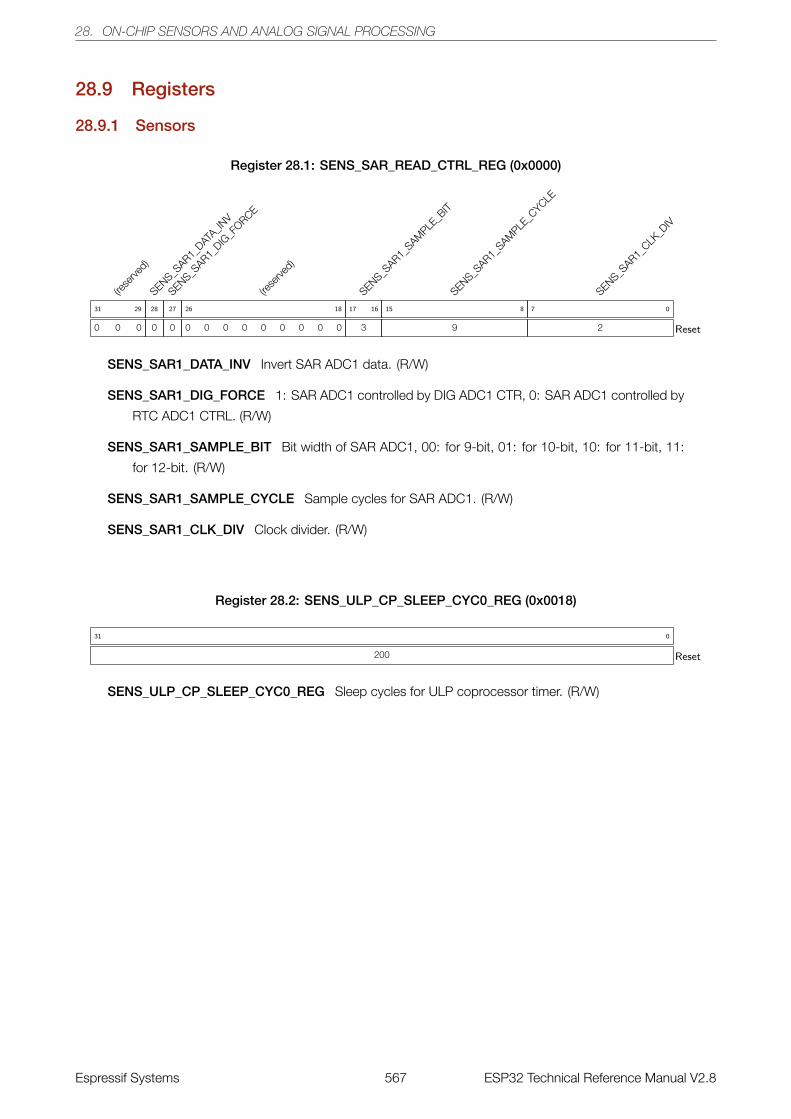
28. ON-CHIP SENSORS AND ANALOG SIGNAL PROCESSING
28.9 Registers
28.9.1 Sensors
Register 28.1: SENS_SAR_READ_CTRL_REG (0x0000)
(rese
rved)
0 0 0
31 29
SENS_SAR1_
DATA_IN
V
0
28
SENS_SAR1_
DIG_F
ORCE
0
27
(rese
rved)
0 0 0 0 0 0 0 0 0
26 18
SENS_SAR1_
SAMPLE
_BIT
3
17 16
SENS_SAR1_
SAMPLE
_CYCLE
9
15 8
SENS_SAR1_
CLK_D
IV
2
7 0
Reset
SENS_SAR1_DATA_INV Invert SAR ADC1 data. (R/W)
SENS_SAR1_DIG_FORCE 1: SAR ADC1 controlled by DIG ADC1 CTR, 0: SAR ADC1 controlled by
RTC ADC1 CTRL. (R/W)
SENS_SAR1_SAMPLE_BIT Bit width of SAR ADC1, 00: for 9-bit, 01: for 10-bit, 10: for 11-bit, 11:
for 12-bit. (R/W)
SENS_SAR1_SAMPLE_CYCLE Sample cycles for SAR ADC1. (R/W)
SENS_SAR1_CLK_DIV Clock divider. (R/W)
Register 28.2: SENS_ULP_CP_SLEEP_CYC0_REG (0x0018)
200
31 0
Reset
SENS_ULP_CP_SLEEP_CYC0_REG Sleep cycles for ULP coprocessor timer. (R/W)
Espressif Systems 567 ESP32 Technical Reference Manual V2.8
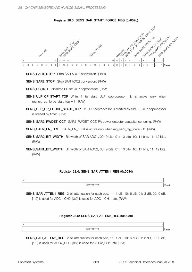
28. ON-CHIP SENSORS AND ANALOG SIGNAL PROCESSING
Register 28.3: SENS_SAR_START_FORCE_REG (0x002c)
(rese
rved)
0 0 0 0 0 0 0 0
31 24
SENS_SAR1_
STOP
0
23
SENS_SAR2_
STOP
0
22
SENS_PC_IN
IT
0 0 0 0 0 0 0 0 0 0 0
21 11
(rese
rved)
0
10
SENS_ULP
_CP_S
TART_
TOP
0
9
SENS_ULP
_CP_F
ORCE_STA
RT_TO
P
0
8
SENS_SAR2_
PWDET_
CCT
0 0 0
7 5
SENS_SAR2_
EN_TEST
0
4
SENS_SAR2_
BIT_W
IDTH
1 1
3 2
SENS_SAR1_
BIT_W
IDTH
1 1
1 0
Reset
SENS_SAR1_STOP Stop SAR ADC1 conversion. (R/W)
SENS_SAR2_STOP Stop SAR ADC2 conversion. (R/W)
SENS_PC_INIT Initialized PC for ULP coprocessor. (R/W)
SENS_ULP_CP_START_TOP Write 1 to start ULP coprocessor; it is active only when
reg_ulp_cp_force_start_top = 1. (R/W)
SENS_ULP_CP_FORCE_START_TOP 1: ULP coprocessor is started by SW, 0: ULP coprocessor
is started by timer. (R/W)
SENS_SAR2_PWDET_CCT SAR2_PWDET_CCT, PA power detector capacitance tuning. (R/W)
SENS_SAR2_EN_TEST SAR2_EN_TEST is active only when reg_sar2_dig_force = 0. (R/W)
SENS_SAR2_BIT_WIDTH Bit width of SAR ADC1, 00: 9 bits, 01: 10 bits, 10: 11 bits, 11: 12 bits.
(R/W)
SENS_SAR1_BIT_WIDTH Bit width of SAR ADC2, 00: 9 bits, 01: 10 bits, 10: 11 bits, 11: 12 bits.
(R/W)
Register 28.4: SENS_SAR_ATTEN1_REG (0x0034)
0x0FFFFFFFF
31 0
Reset
SENS_SAR_ATTEN1_REG 2-bit attenuation for each pad, 11: 1 dB, 10: 6 dB, 01: 3 dB, 00: 0 dB,
[1:0] is used for ADC1_CH0, [3:2] is used for ADC1_CH1, etc. (R/W)
Register 28.5: SENS_SAR_ATTEN2_REG (0x0038)
0x0FFFFFFFF
31 0
Reset
SENS_SAR_ATTEN2_REG 2-bit attenuation for each pad, 11: 1 dB, 10: 6 dB, 01: 3 dB, 00: 0 dB,
[1:0] is used for ADC2_CH0, [3:2] is used for ADC2_CH1, etc (R/W)
Espressif Systems 568 ESP32 Technical Reference Manual V2.8
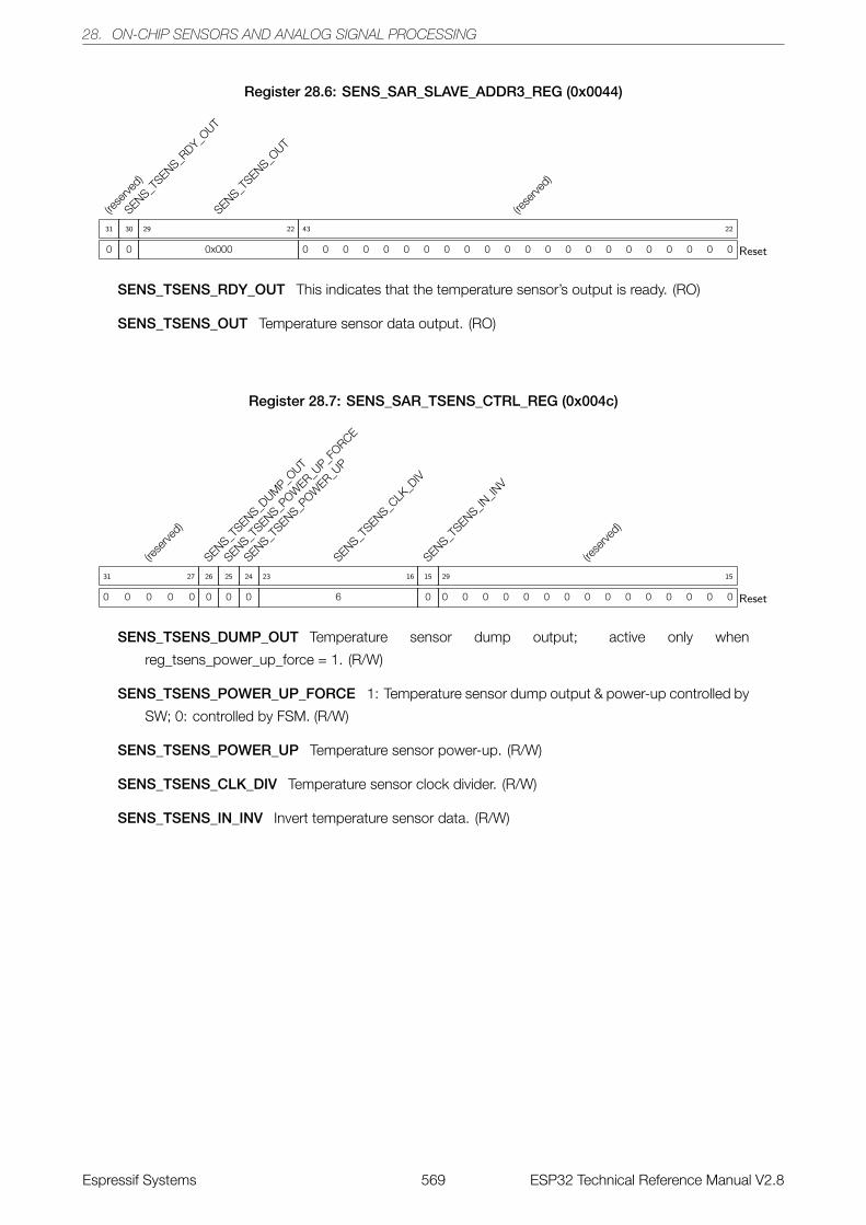
28. ON-CHIP SENSORS AND ANALOG SIGNAL PROCESSING
Register 28.6: SENS_SAR_SLAVE_ADDR3_REG (0x0044)
(rese
rved)
0
31
SENS_TSENS_R
DY_OUT
0
30
SENS_TSENS_O
UT
0x000
29 22
(rese
rved)
0 0 0 0 0 0 0 0 0 0 0 0 0 0 0 0 0 0 0 0 0 0
43 22
Reset
SENS_TSENS_RDY_OUT This indicates that the temperature sensor’s output is ready. (RO)
SENS_TSENS_OUT Temperature sensor data output. (RO)
Register 28.7: SENS_SAR_TSENS_CTRL_REG (0x004c)
(rese
rved)
0 0 0 0 0
31 27
SENS_TSENS_D
UMP_O
UT
0
26
SENS_TSENS_P
OWER_U
P_FORCE
0
25
SENS_TSENS_P
OWER_U
P
0
24
SENS_TSENS_C
LK_D
IV
6
23 16
SENS_TSENS_IN
_INV
0
15
(rese
rved)
0 0 0 0 0 0 0 0 0 0 0 0 0 0 0
29 15
Reset
SENS_TSENS_DUMP_OUT Temperature sensor dump output; active only when
reg_tsens_power_up_force = 1. (R/W)
SENS_TSENS_POWER_UP_FORCE 1: Temperature sensor dump output & power-up controlled by
SW; 0: controlled by FSM. (R/W)
SENS_TSENS_POWER_UP Temperature sensor power-up. (R/W)
SENS_TSENS_CLK_DIV Temperature sensor clock divider. (R/W)
SENS_TSENS_IN_INV Invert temperature sensor data. (R/W)
Espressif Systems 569 ESP32 Technical Reference Manual V2.8
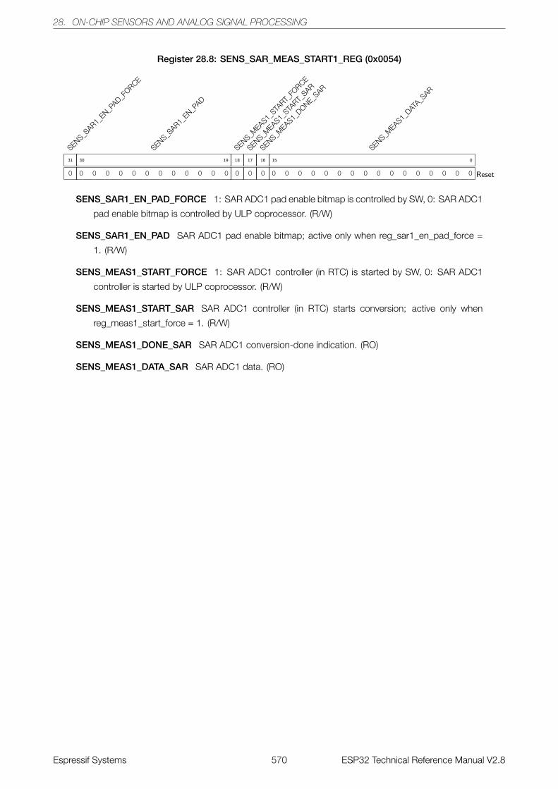
28. ON-CHIP SENSORS AND ANALOG SIGNAL PROCESSING
Register 28.8: SENS_SAR_MEAS_START1_REG (0x0054)
SENS_SAR1_
EN_PAD_F
ORCE
0
31
SENS_SAR1_
EN_PAD
0 0 0 0 0 0 0 0 0 0 0 0
30 19
SENS_MEAS1_
START_
FORCE
0
18
SENS_MEAS1_
START_
SAR
0
17
SENS_MEAS1_
DONE_SAR
0
16
SENS_MEAS1_
DATA_S
AR
0 0 0 0 0 0 0 0 0 0 0 0 0 0 0 0
15 0
Reset
SENS_SAR1_EN_PAD_FORCE 1: SAR ADC1 pad enable bitmap is controlled by SW, 0: SAR ADC1
pad enable bitmap is controlled by ULP coprocessor. (R/W)
SENS_SAR1_EN_PAD SAR ADC1 pad enable bitmap; active only when reg_sar1_en_pad_force =
1. (R/W)
SENS_MEAS1_START_FORCE 1: SAR ADC1 controller (in RTC) is started by SW, 0: SAR ADC1
controller is started by ULP coprocessor. (R/W)
SENS_MEAS1_START_SAR SAR ADC1 controller (in RTC) starts conversion; active only when
reg_meas1_start_force = 1. (R/W)
SENS_MEAS1_DONE_SAR SAR ADC1 conversion-done indication. (RO)
SENS_MEAS1_DATA_SAR SAR ADC1 data. (RO)
Espressif Systems 570 ESP32 Technical Reference Manual V2.8
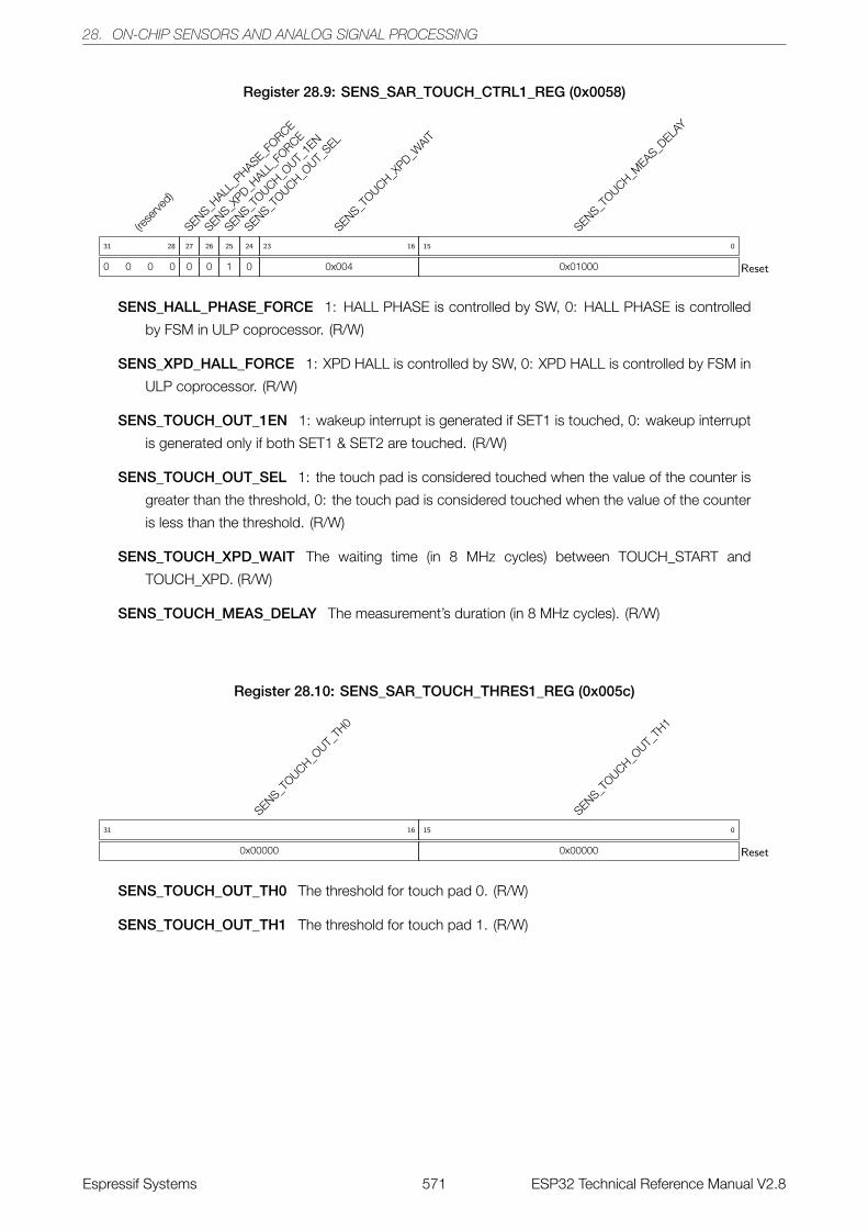
28. ON-CHIP SENSORS AND ANALOG SIGNAL PROCESSING
Register 28.9: SENS_SAR_TOUCH_CTRL1_REG (0x0058)
(rese
rved)
0 0 0 0
31 28
SENS_HALL
_PHASE_F
ORCE
0
27
SENS_XPD_H
ALL_F
ORCE
0
26
SENS_TOUCH_O
UT_1E
N
1
25
SENS_TOUCH_O
UT_SEL
0
24
SENS_TOUCH_X
PD_WAIT
0x004
23 16
SENS_TOUCH_M
EAS_DELA
Y
0x01000
15 0
Reset
SENS_HALL_PHASE_FORCE 1: HALL PHASE is controlled by SW, 0: HALL PHASE is controlled
by FSM in ULP coprocessor. (R/W)
SENS_XPD_HALL_FORCE 1: XPD HALL is controlled by SW, 0: XPD HALL is controlled by FSM in
ULP coprocessor. (R/W)
SENS_TOUCH_OUT_1EN 1: wakeup interrupt is generated if SET1 is touched, 0: wakeup interrupt
is generated only if both SET1 & SET2 are touched. (R/W)
SENS_TOUCH_OUT_SEL 1: the touch pad is considered touched when the value of the counter is
greater than the threshold, 0: the touch pad is considered touched when the value of the counter
is less than the threshold. (R/W)
SENS_TOUCH_XPD_WAIT The waiting time (in 8 MHz cycles) between TOUCH_START and
TOUCH_XPD. (R/W)
SENS_TOUCH_MEAS_DELAY The measurement’s duration (in 8 MHz cycles). (R/W)
Register 28.10: SENS_SAR_TOUCH_THRES1_REG (0x005c)
SENS_TOUCH_O
UT_TH
0
0x00000
31 16
SENS_TOUCH_O
UT_TH
1
0x00000
15 0
Reset
SENS_TOUCH_OUT_TH0 The threshold for touch pad 0. (R/W)
SENS_TOUCH_OUT_TH1 The threshold for touch pad 1. (R/W)
Espressif Systems 571 ESP32 Technical Reference Manual V2.8

28. ON-CHIP SENSORS AND ANALOG SIGNAL PROCESSING
Register 28.11: SENS_SAR_TOUCH_THRES2_REG (0x0060)
SENS_TOUCH_O
UT_TH
2
0x00000
31 16
SENS_TOUCH_O
UT_TH
3
0x00000
15 0
Reset
SENS_TOUCH_OUT_TH2 The threshold for touch pad 2. (R/W)
SENS_TOUCH_OUT_TH3 The threshold for touch pad 3. (R/W)
Register 28.12: SENS_SAR_TOUCH_THRES3_REG (0x0064)
SENS_TOUCH_O
UT_TH
4
0x00000
31 16
SENS_TOUCH_O
UT_TH
5
0x00000
15 0
Reset
SENS_TOUCH_OUT_TH4 The threshold for touch pad 4. (R/W)
SENS_TOUCH_OUT_TH5 The threshold for touch pad 5. (R/W)
Register 28.13: SENS_SAR_TOUCH_THRES4_REG (0x0068)
SENS_TOUCH_O
UT_TH
6
0x00000
31 16
SENS_TOUCH_O
UT_TH
7
0x00000
15 0
Reset
SENS_TOUCH_OUT_TH6 The threshold for touch pad 6. (R/W)
SENS_TOUCH_OUT_TH7 The threshold for touch pad 7. (R/W)
Espressif Systems 572 ESP32 Technical Reference Manual V2.8
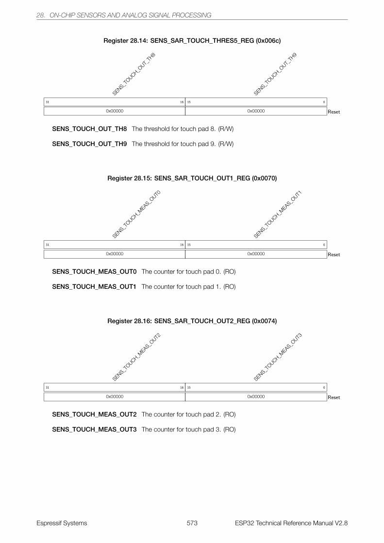
28. ON-CHIP SENSORS AND ANALOG SIGNAL PROCESSING
Register 28.14: SENS_SAR_TOUCH_THRES5_REG (0x006c)
SENS_TOUCH_O
UT_TH
8
0x00000
31 16
SENS_TOUCH_O
UT_TH
9
0x00000
15 0
Reset
SENS_TOUCH_OUT_TH8 The threshold for touch pad 8. (R/W)
SENS_TOUCH_OUT_TH9 The threshold for touch pad 9. (R/W)
Register 28.15: SENS_SAR_TOUCH_OUT1_REG (0x0070)
SENS_TOUCH_M
EAS_OUT0
0x00000
31 16
SENS_TOUCH_M
EAS_OUT1
0x00000
15 0
Reset
SENS_TOUCH_MEAS_OUT0 The counter for touch pad 0. (RO)
SENS_TOUCH_MEAS_OUT1 The counter for touch pad 1. (RO)
Register 28.16: SENS_SAR_TOUCH_OUT2_REG (0x0074)
SENS_TOUCH_M
EAS_OUT2
0x00000
31 16
SENS_TOUCH_M
EAS_OUT3
0x00000
15 0
Reset
SENS_TOUCH_MEAS_OUT2 The counter for touch pad 2. (RO)
SENS_TOUCH_MEAS_OUT3 The counter for touch pad 3. (RO)
Espressif Systems 573 ESP32 Technical Reference Manual V2.8
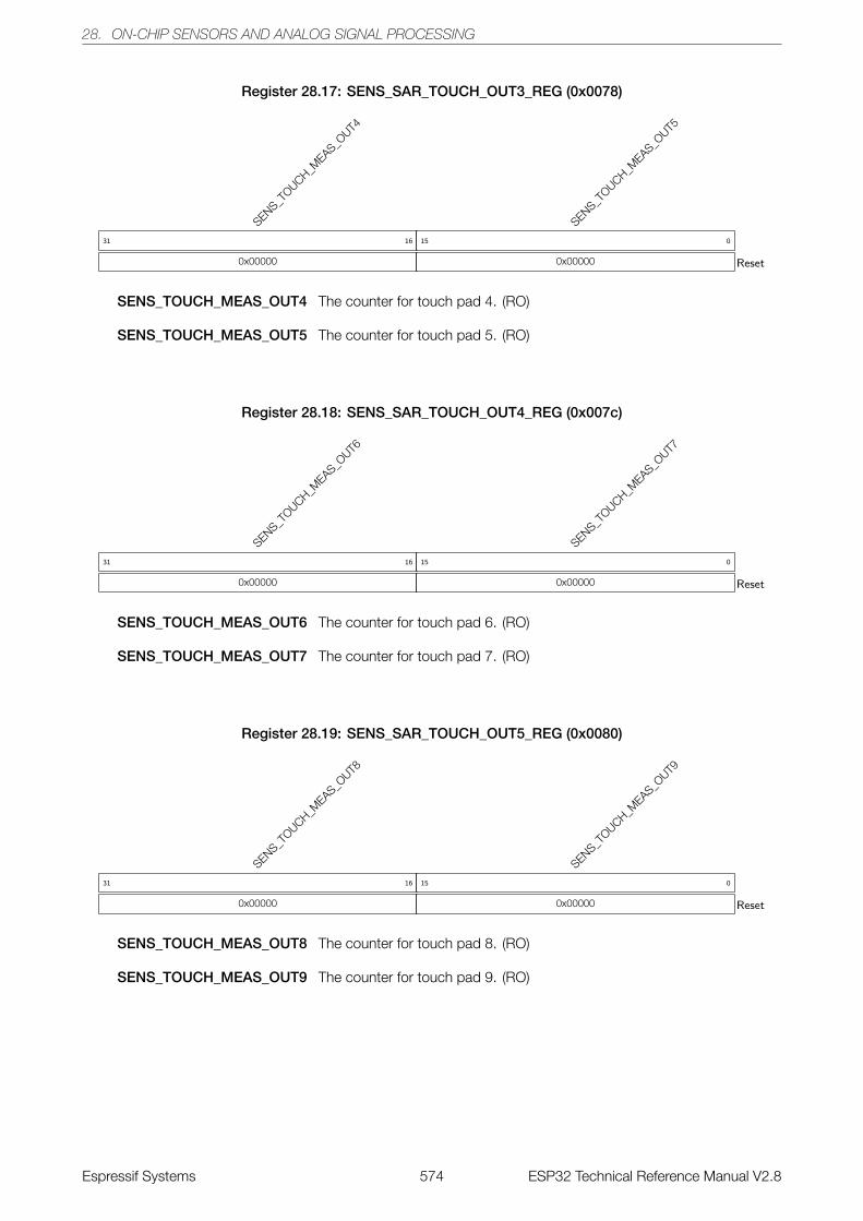
28. ON-CHIP SENSORS AND ANALOG SIGNAL PROCESSING
Register 28.17: SENS_SAR_TOUCH_OUT3_REG (0x0078)
SENS_TOUCH_M
EAS_OUT4
0x00000
31 16
SENS_TOUCH_M
EAS_OUT5
0x00000
15 0
Reset
SENS_TOUCH_MEAS_OUT4 The counter for touch pad 4. (RO)
SENS_TOUCH_MEAS_OUT5 The counter for touch pad 5. (RO)
Register 28.18: SENS_SAR_TOUCH_OUT4_REG (0x007c)
SENS_TOUCH_M
EAS_OUT6
0x00000
31 16
SENS_TOUCH_M
EAS_OUT7
0x00000
15 0
Reset
SENS_TOUCH_MEAS_OUT6 The counter for touch pad 6. (RO)
SENS_TOUCH_MEAS_OUT7 The counter for touch pad 7. (RO)
Register 28.19: SENS_SAR_TOUCH_OUT5_REG (0x0080)
SENS_TOUCH_M
EAS_OUT8
0x00000
31 16
SENS_TOUCH_M
EAS_OUT9
0x00000
15 0
Reset
SENS_TOUCH_MEAS_OUT8 The counter for touch pad 8. (RO)
SENS_TOUCH_MEAS_OUT9 The counter for touch pad 9. (RO)
Espressif Systems 574 ESP32 Technical Reference Manual V2.8
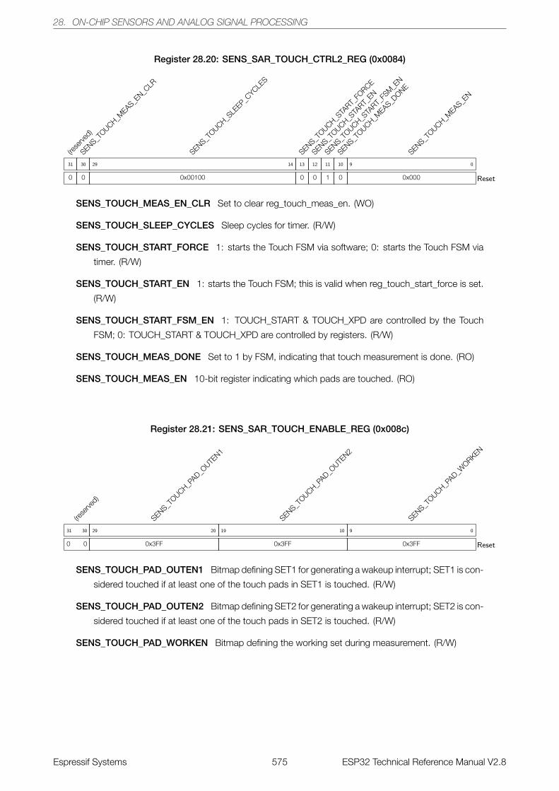
28. ON-CHIP SENSORS AND ANALOG SIGNAL PROCESSING
Register 28.20: SENS_SAR_TOUCH_CTRL2_REG (0x0084)
(rese
rved)
0
31
SENS_TOUCH_M
EAS_EN_C
LR
0
30
SENS_TOUCH_S
LEEP_C
YCLES
0x00100
29 14
SENS_TOUCH_S
TART_
FORCE
0
13
SENS_TOUCH_S
TART_
EN
0
12
SENS_TOUCH_S
TART_
FSM
_EN
1
11
SENS_TOUCH_M
EAS_DONE
0
10
SENS_TOUCH_M
EAS_EN
0x000
9 0
Reset
SENS_TOUCH_MEAS_EN_CLR Set to clear reg_touch_meas_en. (WO)
SENS_TOUCH_SLEEP_CYCLES Sleep cycles for timer. (R/W)
SENS_TOUCH_START_FORCE 1: starts the Touch FSM via software; 0: starts the Touch FSM via
timer. (R/W)
SENS_TOUCH_START_EN 1: starts the Touch FSM; this is valid when reg_touch_start_force is set.
(R/W)
SENS_TOUCH_START_FSM_EN 1: TOUCH_START & TOUCH_XPD are controlled by the Touch
FSM; 0: TOUCH_START & TOUCH_XPD are controlled by registers. (R/W)
SENS_TOUCH_MEAS_DONE Set to 1 by FSM, indicating that touch measurement is done. (RO)
SENS_TOUCH_MEAS_EN 10-bit register indicating which pads are touched. (RO)
Register 28.21: SENS_SAR_TOUCH_ENABLE_REG (0x008c)
(rese
rved)
0 0
31 30
SENS_TOUCH_P
AD_OUTE
N1
0x3FF
29 20
SENS_TOUCH_P
AD_OUTE
N2
0x3FF
19 10
SENS_TOUCH_P
AD_WORKEN
0x3FF
9 0
Reset
SENS_TOUCH_PAD_OUTEN1 Bitmap defining SET1 for generating a wakeup interrupt; SET1 is con-
sidered touched if at least one of the touch pads in SET1 is touched. (R/W)
SENS_TOUCH_PAD_OUTEN2 Bitmap defining SET2 for generating a wakeup interrupt; SET2 is con-
sidered touched if at least one of the touch pads in SET2 is touched. (R/W)
SENS_TOUCH_PAD_WORKEN Bitmap defining the working set during measurement. (R/W)
Espressif Systems 575 ESP32 Technical Reference Manual V2.8
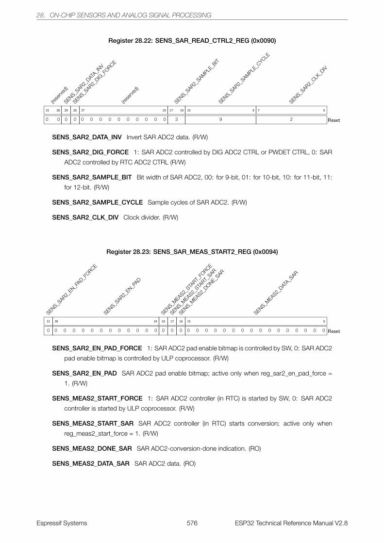
28. ON-CHIP SENSORS AND ANALOG SIGNAL PROCESSING
Register 28.22: SENS_SAR_READ_CTRL2_REG (0x0090)
(rese
rved)
0 0
31 30
SENS_SAR2_
DATA_IN
V
0
29
SENS_SAR2_
DIG_F
ORCE
0
28
(rese
rved)
0 0 0 0 0 0 0 0 0 0
27 18
SENS_SAR2_
SAMPLE
_BIT
3
17 16
SENS_SAR2_
SAMPLE
_CYCLE
9
15 8
SENS_SAR2_
CLK_D
IV
2
7 0
Reset
SENS_SAR2_DATA_INV Invert SAR ADC2 data. (R/W)
SENS_SAR2_DIG_FORCE 1: SAR ADC2 controlled by DIG ADC2 CTRL or PWDET CTRL, 0: SAR
ADC2 controlled by RTC ADC2 CTRL (R/W)
SENS_SAR2_SAMPLE_BIT Bit width of SAR ADC2, 00: for 9-bit, 01: for 10-bit, 10: for 11-bit, 11:
for 12-bit. (R/W)
SENS_SAR2_SAMPLE_CYCLE Sample cycles of SAR ADC2. (R/W)
SENS_SAR2_CLK_DIV Clock divider. (R/W)
Register 28.23: SENS_SAR_MEAS_START2_REG (0x0094)
SENS_SAR2_
EN_PAD_F
ORCE
0
31
SENS_SAR2_
EN_PAD
0 0 0 0 0 0 0 0 0 0 0 0
30 19
SENS_MEAS2_
START_
FORCE
0
18
SENS_MEAS2_
START_
SAR
0
17
SENS_MEAS2_
DONE_SAR
0
16
SENS_MEAS2_
DATA_S
AR
0 0 0 0 0 0 0 0 0 0 0 0 0 0 0 0
15 0
Reset
SENS_SAR2_EN_PAD_FORCE 1: SAR ADC2 pad enable bitmap is controlled by SW, 0: SAR ADC2
pad enable bitmap is controlled by ULP coprocessor. (R/W)
SENS_SAR2_EN_PAD SAR ADC2 pad enable bitmap; active only when reg_sar2_en_pad_force =
1. (R/W)
SENS_MEAS2_START_FORCE 1: SAR ADC2 controller (in RTC) is started by SW, 0: SAR ADC2
controller is started by ULP coprocessor. (R/W)
SENS_MEAS2_START_SAR SAR ADC2 controller (in RTC) starts conversion; active only when
reg_meas2_start_force = 1. (R/W)
SENS_MEAS2_DONE_SAR SAR ADC2-conversion-done indication. (RO)
SENS_MEAS2_DATA_SAR SAR ADC2 data. (RO)
Espressif Systems 576 ESP32 Technical Reference Manual V2.8
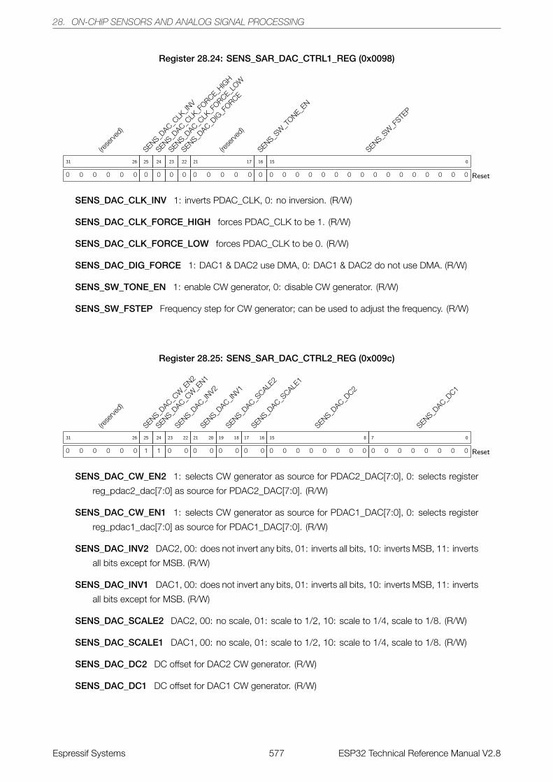
28. ON-CHIP SENSORS AND ANALOG SIGNAL PROCESSING
Register 28.24: SENS_SAR_DAC_CTRL1_REG (0x0098)
(rese
rved)
0 0 0 0 0 0
31 26
SENS_DAC_C
LK_IN
V
0
25
SENS_DAC_C
LK_F
ORCE_HIG
H
0
24
SENS_DAC_C
LK_F
ORCE_LOW
0
23
SENS_DAC_D
IG_F
ORCE
0
22
(rese
rved)
0 0 0 0 0
21 17
SENS_SW
_TONE_E
N
0
16
SENS_SW
_FSTE
P
0 0 0 0 0 0 0 0 0 0 0 0 0 0 0 0
15 0
Reset
SENS_DAC_CLK_INV 1: inverts PDAC_CLK, 0: no inversion. (R/W)
SENS_DAC_CLK_FORCE_HIGH forces PDAC_CLK to be 1. (R/W)
SENS_DAC_CLK_FORCE_LOW forces PDAC_CLK to be 0. (R/W)
SENS_DAC_DIG_FORCE 1: DAC1 & DAC2 use DMA, 0: DAC1 & DAC2 do not use DMA. (R/W)
SENS_SW_TONE_EN 1: enable CW generator, 0: disable CW generator. (R/W)
SENS_SW_FSTEP Frequency step for CW generator; can be used to adjust the frequency. (R/W)
Register 28.25: SENS_SAR_DAC_CTRL2_REG (0x009c)
(rese
rved)
0 0 0 0 0 0
31 26
SENS_DAC_C
W_E
N2
1
25
SENS_DAC_C
W_E
N1
1
24
SENS_DAC_IN
V2
0 0
23 22
SENS_DAC_IN
V1
0 0
21 20
SENS_DAC_S
CALE2
0 0
19 18
SENS_DAC_S
CALE1
0 0
17 16
SENS_DAC_D
C2
0 0 0 0 0 0 0 0
15 8
SENS_DAC_D
C1
0 0 0 0 0 0 0 0
7 0
Reset
SENS_DAC_CW_EN2 1: selects CW generator as source for PDAC2_DAC[7:0], 0: selects register
reg_pdac2_dac[7:0] as source for PDAC2_DAC[7:0]. (R/W)
SENS_DAC_CW_EN1 1: selects CW generator as source for PDAC1_DAC[7:0], 0: selects register
reg_pdac1_dac[7:0] as source for PDAC1_DAC[7:0]. (R/W)
SENS_DAC_INV2 DAC2, 00: does not invert any bits, 01: inverts all bits, 10: inverts MSB, 11: inverts
all bits except for MSB. (R/W)
SENS_DAC_INV1 DAC1, 00: does not invert any bits, 01: inverts all bits, 10: inverts MSB, 11: inverts
all bits except for MSB. (R/W)
SENS_DAC_SCALE2 DAC2, 00: no scale, 01: scale to 1/2, 10: scale to 1/4, scale to 1/8. (R/W)
SENS_DAC_SCALE1 DAC1, 00: no scale, 01: scale to 1/2, 10: scale to 1/4, scale to 1/8. (R/W)
SENS_DAC_DC2 DC offset for DAC2 CW generator. (R/W)
SENS_DAC_DC1 DC offset for DAC1 CW generator. (R/W)
Espressif Systems 577 ESP32 Technical Reference Manual V2.8
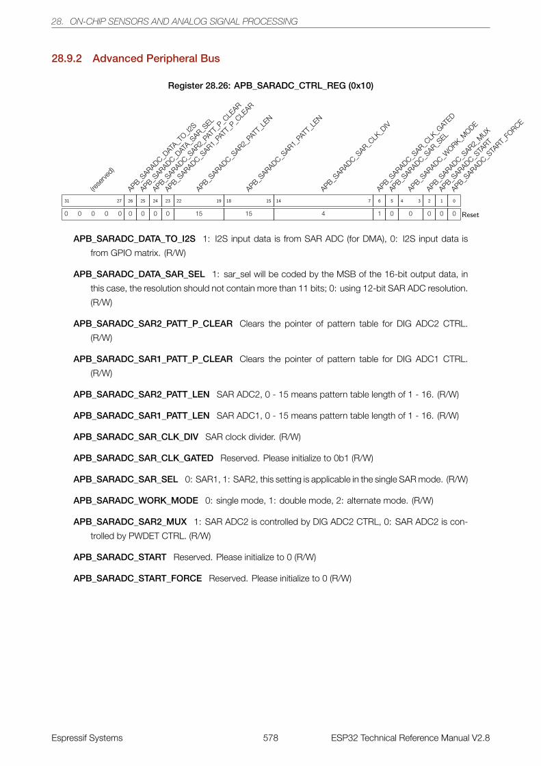
28. ON-CHIP SENSORS AND ANALOG SIGNAL PROCESSING
28.9.2 Advanced Peripheral Bus
Register 28.26: APB_SARADC_CTRL_REG (0x10)
(rese
rved)
0 0 0 0 0
31 27
APB_SARADC_D
ATA_T
O_I2S
0
26
APB_SARADC_D
ATA_S
AR_SEL
0
25
APB_SARADC_S
AR2_PA
TT_P
_CLE
AR
0
24
APB_SARADC_S
AR1_PA
TT_P
_CLE
AR
0
23
APB_SARADC_S
AR2_PA
TT_L
EN
15
22 19
APB_SARADC_S
AR1_PA
TT_L
EN
15
18 15
APB_SARADC_S
AR_CLK
_DIV
4
14 7
APB_SARADC_S
AR_CLK
_GAT
ED
1
6
APB_SARADC_S
AR_SEL
0
5
APB_SARADC_W
ORK_MODE
0
4 3
APB_SARADC_S
AR2_M
UX
0
2
APB_SARADC_S
TART
0
1
APB_SARADC_S
TART_
FORCE
0
0
Reset
APB_SARADC_DATA_TO_I2S 1: I2S input data is from SAR ADC (for DMA), 0: I2S input data is
from GPIO matrix. (R/W)
APB_SARADC_DATA_SAR_SEL 1: sar_sel will be coded by the MSB of the 16-bit output data, in
this case, the resolution should not contain more than 11 bits; 0: using 12-bit SAR ADC resolution.
(R/W)
APB_SARADC_SAR2_PATT_P_CLEAR Clears the pointer of pattern table for DIG ADC2 CTRL.
(R/W)
APB_SARADC_SAR1_PATT_P_CLEAR Clears the pointer of pattern table for DIG ADC1 CTRL.
(R/W)
APB_SARADC_SAR2_PATT_LEN SAR ADC2, 0 - 15 means pattern table length of 1 - 16. (R/W)
APB_SARADC_SAR1_PATT_LEN SAR ADC1, 0 - 15 means pattern table length of 1 - 16. (R/W)
APB_SARADC_SAR_CLK_DIV SAR clock divider. (R/W)
APB_SARADC_SAR_CLK_GATED Reserved. Please initialize to 0b1 (R/W)
APB_SARADC_SAR_SEL 0: SAR1, 1: SAR2, this setting is applicable in the single SAR mode. (R/W)
APB_SARADC_WORK_MODE 0: single mode, 1: double mode, 2: alternate mode. (R/W)
APB_SARADC_SAR2_MUX 1: SAR ADC2 is controlled by DIG ADC2 CTRL, 0: SAR ADC2 is con-
trolled by PWDET CTRL. (R/W)
APB_SARADC_START Reserved. Please initialize to 0 (R/W)
APB_SARADC_START_FORCE Reserved. Please initialize to 0 (R/W)
Espressif Systems 578 ESP32 Technical Reference Manual V2.8
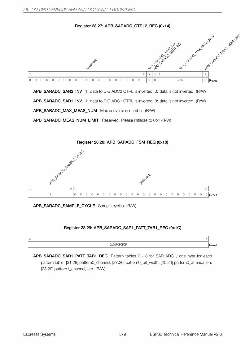
28. ON-CHIP SENSORS AND ANALOG SIGNAL PROCESSING
Register 28.27: APB_SARADC_CTRL2_REG (0x14)
(rese
rved)
0 0 0 0 0 0 0 0 0 0 0 0 0 0 0 0 0 0 0 0 0
31 11
APB_SARADC_S
AR2_IN
V
0
10
APB_SARADC_S
AR1_IN
V
0
9
APB_SARADC_M
AX_M
EAS_NUM
255
8 1
APB_SARADC_M
EAS_NUM
_LIM
IT
0
0
Reset
APB_SARADC_SAR2_INV 1: data to DIG ADC2 CTRL is inverted, 0: data is not inverted. (R/W)
APB_SARADC_SAR1_INV 1: data to DIG ADC1 CTRL is inverted, 0: data is not inverted. (R/W)
APB_SARADC_MAX_MEAS_NUM Max conversion number. (R/W)
APB_SARADC_MEAS_NUM_LIMIT Reserved. Please initialize to 0b1 (R/W)
Register 28.28: APB_SARADC_FSM_REG (0x18)
APB_SARADC_S
AMPLE
_CYCLE
2
31 24
(rese
rved)
0 0 0 0 0 0 0 0 0 0 0 0 0 0 0 0 0 0 0 0 0 0 0 0
47 24
Reset
APB_SARADC_SAMPLE_CYCLE Sample cycles. (R/W)
Register 28.29: APB_SARADC_SAR1_PATT_TAB1_REG (0x1C)
0x00F0F0F0F
31 0
Reset
APB_SARADC_SAR1_PATT_TAB1_REG Pattern tables 0 - 3 for SAR ADC1, one byte for each
pattern table: [31:28] pattern0_channel, [27:26] pattern0_bit_width, [25:24] pattern0_attenuation,
[23:20] pattern1_channel, etc. (R/W)
Espressif Systems 579 ESP32 Technical Reference Manual V2.8
28. ON-CHIP SENSORS AND ANALOG SIGNAL PROCESSING
Register 28.30: APB_SARADC_SAR1_PATT_TAB2_REG (0x20)
0x00F0F0F0F
31 0
Reset
APB_SARADC_SAR1_PATT_TAB2_REG Pattern tables 4 - 7 for SAR ADC1, one byte for each
pattern table: [31:28] pattern4_channel, [27:26] pattern4_bit_width, [25:24] pattern4_attenuation,
[23:20] pattern5_channel, etc. (R/W)
Register 28.31: APB_SARADC_SAR1_PATT_TAB3_REG (0x24)
0x00F0F0F0F
31 0
Reset
APB_SARADC_SAR1_PATT_TAB3_REG Pattern tables 8 - 11 for SAR ADC1, one byte for each
pattern table: [31:28] pattern8_channel, [27:26] pattern8_bit_width, [25:24] pattern8_attenuation,
[23:20] pattern9_channel, etc. (R/W)
Register 28.32: APB_SARADC_SAR1_PATT_TAB4_REG (0x28)
0x00F0F0F0F
31 0
Reset
APB_SARADC_SAR1_PATT_TAB4_REG Pattern tables 12 - 15 for SAR ADC1, one byte for
each pattern table: [31:28] pattern12_channel, [27:26] pattern12_bit_width, [25:24] pat-
tern12_attenuation, [23:20] pattern13_channel, etc. (R/W)
Register 28.33: APB_SARADC_SAR2_PATT_TAB1_REG (0x2C)
0x00F0F0F0F
31 0
Reset
APB_SARADC_SAR2_PATT_TAB1_REG Pattern tables 0 - 3 for SAR ADC2, one byte for each
pattern table: [31:28] pattern0_channel, [27:26] pattern0_bit_width, [25:24] pattern0_attenuation,
[23:20] pattern1_channel, etc. (R/W)
Register 28.34: APB_SARADC_SAR2_PATT_TAB2_REG (0x30)
0x00F0F0F0F
31 0
Reset
APB_SARADC_SAR2_PATT_TAB2_REG Pattern tables 4 - 7 for SAR ADC2, one byte for each
pattern table: [31:28] pattern4_channel, [27:26] pattern4_bit_width, [25:24] pattern4_attenuation,
[23:20] pattern5_channel, etc. (R/W)
Espressif Systems 580 ESP32 Technical Reference Manual V2.8
28. ON-CHIP SENSORS AND ANALOG SIGNAL PROCESSING
Register 28.35: APB_SARADC_SAR2_PATT_TAB3_REG (0x34)
0x00F0F0F0F
31 0
Reset
APB_SARADC_SAR2_PATT_TAB3_REG Pattern tables 8 - 11 for SAR ADC2, one byte for each
pattern table: [31:28] pattern8_channel, [27:26] pattern8_bit_width, [25:24] pattern8_attenuation,
[23:20] pattern9_channel, etc. (R/W)
Register 28.36: APB_SARADC_SAR2_PATT_TAB4_REG (0x38)
0x00F0F0F0F
31 0
Reset
APB_SARADC_SAR2_PATT_TAB4_REG Pattern tables 12 - 15 for SAR ADC2, one byte for
each pattern table: [31:28] pattern12_channel, [27:26] pattern12_bit_width, [25:24] pat-
tern12_attenuation, [23:20] pattern13_channel, etc. (R/W)
28.9.3 RTC I/O
For details, please refer to Section Registers in Chapter IO_MUX and GPIO Matrix.
Espressif Systems 581 ESP32 Technical Reference Manual V2.8
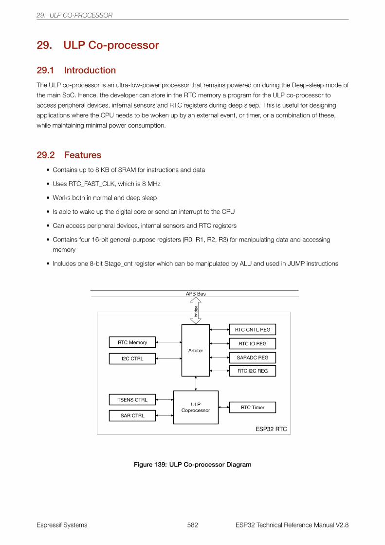
29. ULP CO-PROCESSOR
29. ULP Co-processor
29.1 Introduction
The ULP co-processor is an ultra-low-power processor that remains powered on during the Deep-sleep mode of
the main SoC. Hence, the developer can store in the RTC memory a program for the ULP co-processor to
access peripheral devices, internal sensors and RTC registers during deep sleep. This is useful for designing
applications where the CPU needs to be woken up by an external event, or timer, or a combination of these,
while maintaining minimal power consumption.
29.2 Features
• Contains up to 8 KB of SRAM for instructions and data
• Uses RTC_FAST_CLK, which is 8 MHz
• Works both in normal and deep sleep
• Is able to wake up the digital core or send an interrupt to the CPU
• Can access peripheral devices, internal sensors and RTC registers
• Contains four 16-bit general-purpose registers (R0, R1, R2, R3) for manipulating data and accessing
memory
• Includes one 8-bit Stage_cnt register which can be manipulated by ALU and used in JUMP instructions
RTC Memory
I2C CTRL
RTC CNTL REG
SAR CTRL
TSENS CTRL
ESP32 RTC
APB Bus
brid
ge
RTC IO REG
RTC I2C REG
SARADC REG
Arbiter
ULPCoprocessor
RTC Timer
Figure 139: ULP Co-processor Diagram
Espressif Systems 582 ESP32 Technical Reference Manual V2.8
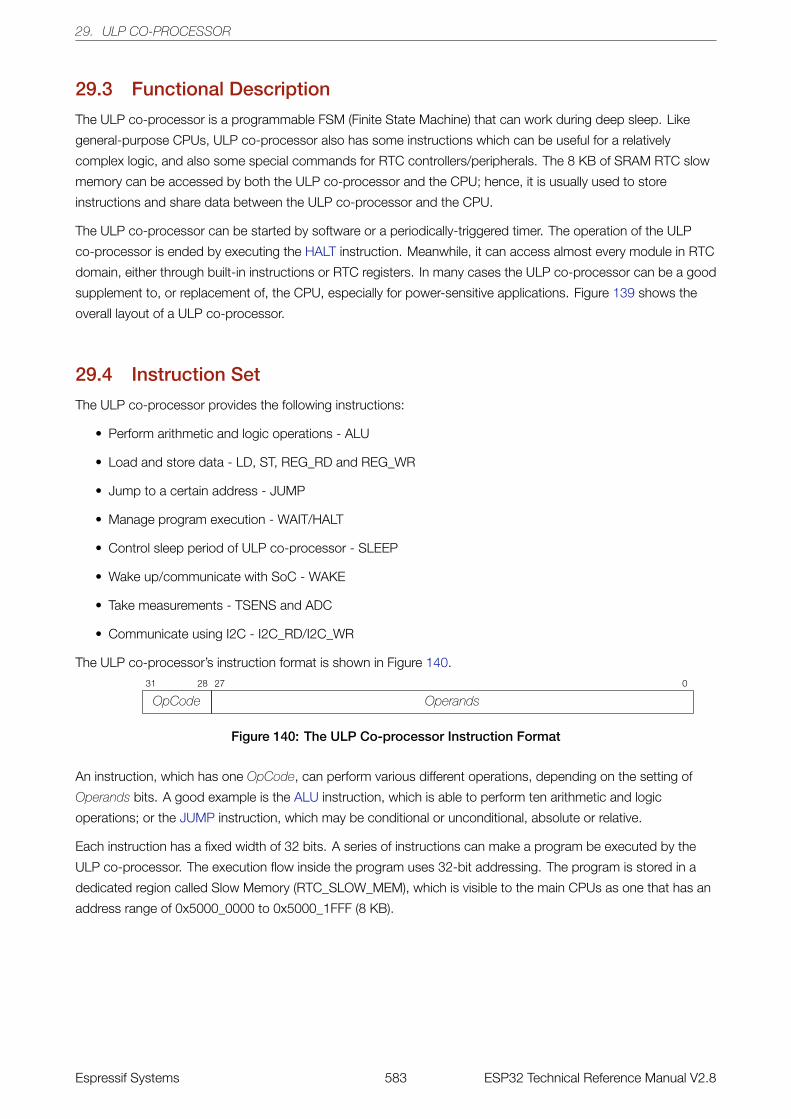
29. ULP CO-PROCESSOR
29.3 Functional Description
The ULP co-processor is a programmable FSM (Finite State Machine) that can work during deep sleep. Like
general-purpose CPUs, ULP co-processor also has some instructions which can be useful for a relatively
complex logic, and also some special commands for RTC controllers/peripherals. The 8 KB of SRAM RTC slow
memory can be accessed by both the ULP co-processor and the CPU; hence, it is usually used to store
instructions and share data between the ULP co-processor and the CPU.
The ULP co-processor can be started by software or a periodically-triggered timer. The operation of the ULP
co-processor is ended by executing the HALT instruction. Meanwhile, it can access almost every module in RTC
domain, either through built-in instructions or RTC registers. In many cases the ULP co-processor can be a good
supplement to, or replacement of, the CPU, especially for power-sensitive applications. Figure 139 shows the
overall layout of a ULP co-processor.
29.4 Instruction Set
The ULP co-processor provides the following instructions:
• Perform arithmetic and logic operations - ALU
• Load and store data - LD, ST, REG_RD and REG_WR
• Jump to a certain address - JUMP
• Manage program execution - WAIT/HALT
• Control sleep period of ULP co-processor - SLEEP
• Wake up/communicate with SoC - WAKE
• Take measurements - TSENS and ADC
• Communicate using I2C - I2C_RD/I2C_WR
The ULP co-processor’s instruction format is shown in Figure 140.0272831
OpCode Operands
Figure 140: The ULP Co-processor Instruction Format
An instruction, which has one OpCode, can perform various different operations, depending on the setting of
Operands bits. A good example is the ALU instruction, which is able to perform ten arithmetic and logic
operations; or the JUMP instruction, which may be conditional or unconditional, absolute or relative.
Each instruction has a fixed width of 32 bits. A series of instructions can make a program be executed by the
ULP co-processor. The execution flow inside the program uses 32-bit addressing. The program is stored in a
dedicated region called Slow Memory (RTC_SLOW_MEM), which is visible to the main CPUs as one that has an
address range of 0x5000_0000 to 0x5000_1FFF (8 KB).
Espressif Systems 583 ESP32 Technical Reference Manual V2.8
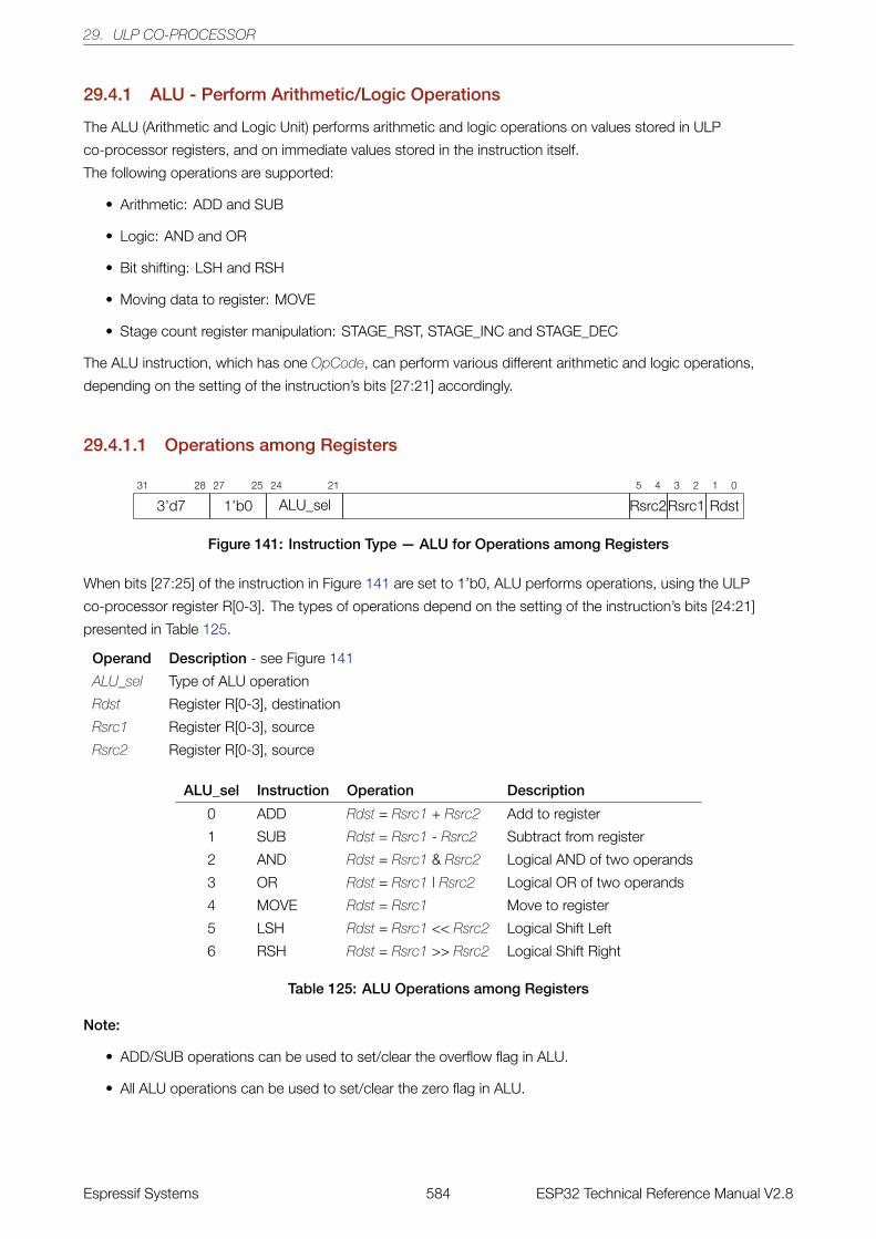
29. ULP CO-PROCESSOR
29.4.1 ALU - Perform Arithmetic/Logic Operations
The ALU (Arithmetic and Logic Unit) performs arithmetic and logic operations on values stored in ULP
co-processor registers, and on immediate values stored in the instruction itself.
The following operations are supported:
• Arithmetic: ADD and SUB
• Logic: AND and OR
• Bit shifting: LSH and RSH
• Moving data to register: MOVE
• Stage count register manipulation: STAGE_RST, STAGE_INC and STAGE_DEC
The ALU instruction, which has one OpCode, can perform various different arithmetic and logic operations,
depending on the setting of the instruction’s bits [27:21] accordingly.
29.4.1.1 Operations among Registers
012345212425272831
3’d7 1’b0 ALU_sel Rsrc2Rsrc1 Rdst
Figure 141: Instruction Type — ALU for Operations among Registers
When bits [27:25] of the instruction in Figure 141 are set to 1’b0, ALU performs operations, using the ULP
co-processor register R[0-3]. The types of operations depend on the setting of the instruction’s bits [24:21]
presented in Table 125.
Operand Description - see Figure 141
ALU_sel Type of ALU operation
Rdst Register R[0-3], destination
Rsrc1 Register R[0-3], source
Rsrc2 Register R[0-3], source
ALU_sel Instruction Operation Description
0 ADD Rdst = Rsrc1 + Rsrc2 Add to register
1 SUB Rdst = Rsrc1 - Rsrc2 Subtract from register
2 AND Rdst = Rsrc1 & Rsrc2 Logical AND of two operands
3 OR Rdst = Rsrc1 | Rsrc2 Logical OR of two operands
4 MOVE Rdst = Rsrc1 Move to register
5 LSH Rdst = Rsrc1 <<�Rsrc2 Logical Shift Left
6 RSH Rdst = Rsrc1 >>�Rsrc2 Logical Shift Right
Table 125: ALU Operations among Registers
Note:
• ADD/SUB operations can be used to set/clear the overflow flag in ALU.
• All ALU operations can be used to set/clear the zero flag in ALU.
Espressif Systems 584 ESP32 Technical Reference Manual V2.8
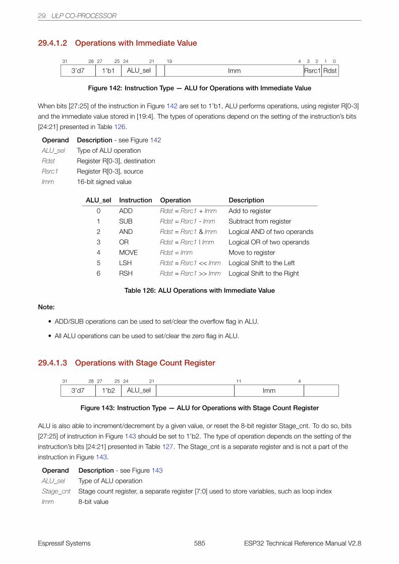
29. ULP CO-PROCESSOR
29.4.1.2 Operations with Immediate Value
0123419212425272831
3’d7 1’b1 ALU_sel Imm Rsrc1 Rdst
Figure 142: Instruction Type — ALU for Operations with Immediate Value
When bits [27:25] of the instruction in Figure 142 are set to 1’b1, ALU performs operations, using register R[0-3]
and the immediate value stored in [19:4]. The types of operations depend on the setting of the instruction’s bits
[24:21] presented in Table 126.
Operand Description - see Figure 142
ALU_sel Type of ALU operation
Rdst Register R[0-3], destination
Rsrc1 Register R[0-3], source
Imm 16-bit signed value
ALU_sel Instruction Operation Description
0 ADD Rdst = Rsrc1 + Imm Add to register
1 SUB Rdst = Rsrc1 - Imm Subtract from register
2 AND Rdst = Rsrc1 & Imm Logical AND of two operands
3 OR Rdst = Rsrc1 | Imm Logical OR of two operands
4 MOVE Rdst = Imm Move to register
5 LSH Rdst = Rsrc1 <<�Imm Logical Shift to the Left
6 RSH Rdst = Rsrc1 >>�Imm Logical Shift to the Right
Table 126: ALU Operations with Immediate Value
Note:
• ADD/SUB operations can be used to set/clear the overflow flag in ALU.
• All ALU operations can be used to set/clear the zero flag in ALU.
29.4.1.3 Operations with Stage Count Register
411212425272831
3’d7 1’b2 ALU_sel Imm
Figure 143: Instruction Type — ALU for Operations with Stage Count Register
ALU is also able to increment/decrement by a given value, or reset the 8-bit register Stage_cnt. To do so, bits
[27:25] of instruction in Figure 143 should be set to 1’b2. The type of operation depends on the setting of the
instruction’s bits [24:21] presented in Table 127. The Stage_cnt is a separate register and is not a part of the
instruction in Figure 143.
Operand Description - see Figure 143
ALU_sel Type of ALU operation
Stage_cnt Stage count register, a separate register [7:0] used to store variables, such as loop index
Imm 8-bit value
Espressif Systems 585 ESP32 Technical Reference Manual V2.8
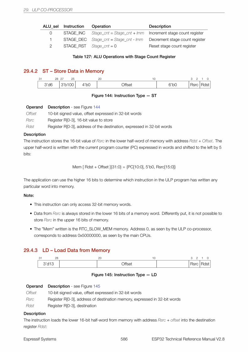
29. ULP CO-PROCESSOR
ALU_sel Instruction Operation Description
0 STAGE_INC Stage_cnt = Stage_cnt + Imm Increment stage count register
1 STAGE_DEC Stage_cnt = Stage_cnt - Imm Decrement stage count register
2 STAGE_RST Stage_cnt = 0 Reset stage count register
Table 127: ALU Operations with Stage Count Register
29.4.2 ST – Store Data in Memory0123102025272831
3’d6 3’b100 4’b0 Offset 6’b0 Rsrc Rdst
Figure 144: Instruction Type — ST
Operand Description - see Figure 144
Offset 10-bit signed value, offset expressed in 32-bit words
Rsrc Register R[0-3], 16-bit value to store
Rdst Register R[0-3], address of the destination, expressed in 32-bit words
Description
The instruction stores the 16-bit value of Rsrc in the lower half-word of memory with address Rdst + Offset. The
upper half-word is written with the current program counter (PC) expressed in words and shifted to the left by 5
bits:
Mem [ Rdst + Offset ]{31:0} = {PC[10:0], 5’b0, Rsrc[15:0]}
The application can use the higher 16 bits to determine which instruction in the ULP program has written any
particular word into memory.
Note:
• This instruction can only access 32-bit memory words.
• Data from Rsrc is always stored in the lower 16 bits of a memory word. Differently put, it is not possible to
store Rsrc in the upper 16 bits of memory.
• The ”Mem” written is the RTC_SLOW_MEM memory. Address 0, as seen by the ULP co-processor,
corresponds to address 0x50000000, as seen by the main CPUs.
29.4.3 LD – Load Data from Memory012310202831
3’d13 Offset Rsrc Rdst
Figure 145: Instruction Type — LD
Operand Description - see Figure 145
Offset 10-bit signed value, offset expressed in 32-bit words
Rsrc Register R[0-3], address of destination memory, expressed in 32-bit words
Rdst Register R[0-3], destination
Description
The instruction loads the lower 16-bit half-word from memory with address Rsrc + offset into the destination
register Rdst:
Espressif Systems 586 ESP32 Technical Reference Manual V2.8
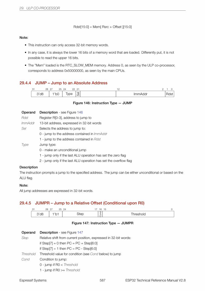
29. ULP CO-PROCESSOR
Rdst[15:0] = Mem[ Rsrc + Offset ][15:0]
Note:
• This instruction can only access 32-bit memory words.
• In any case, it is always the lower 16 bits of a memory word that are loaded. Differently put, it is not
possible to read the upper 16 bits.
• The ”Mem” loaded is the RTC_SLOW_MEM memory. Address 0, as seen by the ULP co-processor,
corresponds to address 0x50000000, as seen by the main CPUs.
29.4.4 JUMP – Jump to an Absolute Address0121221222425272831
3’d8 1’b0 Type Sel ImmAddr Rdst
Figure 146: Instruction Type — JUMP
Operand Description - see Figure 146
Rdst Register R[0-3], address to jump to
ImmAddr 13-bit address, expressed in 32-bit words
Sel Selects the address to jump to:
0 - jump to the address contained in ImmAddr
1 - jump to the address contained in Rdst
Type Jump type:
0 - make an unconditional jump
1 - jump only if the last ALU operation has set the zero flag
2 - jump only if the last ALU operation has set the overflow flag
Description
The instruction prompts a jump to the specified address. The jump can be either unconditional or based on the
ALU flag.
Note:
All jump addresses are expressed in 32-bit words.
29.4.5 JUMPR – Jump to a Relative Offset (Conditional upon R0)01516172425272831
3’d8 1’b1 Step
Con
d
Threshold
Figure 147: Instruction Type — JUMPR
Operand Description - see Figure 147
Step Relative shift from current position, expressed in 32-bit words:
if Step[7] = 0 then PC = PC + Step[6:0]
if Step[7] = 1 then PC = PC - Step[6:0]
Threshold Threshold value for condition (see Cond below) to jump
Cond Condition to jump:
0 - jump if R0 < Threshold
1 - jump if R0 >= Threshold
Espressif Systems 587 ESP32 Technical Reference Manual V2.8
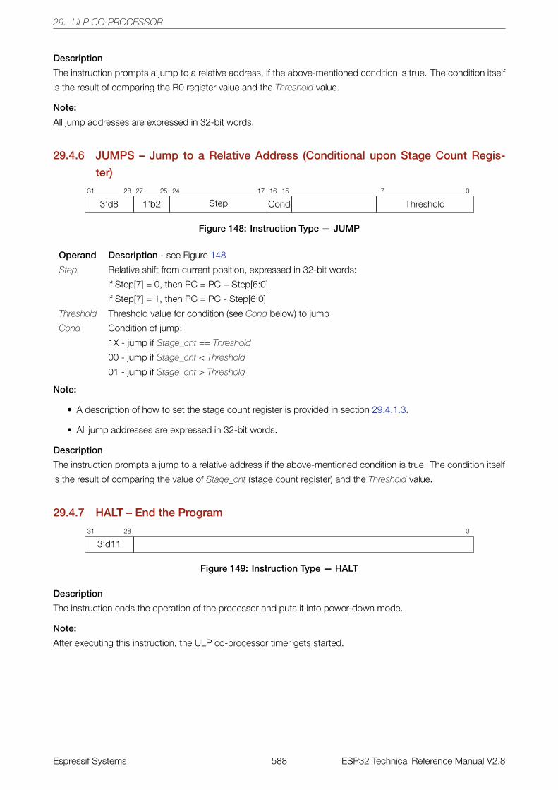
29. ULP CO-PROCESSOR
Description
The instruction prompts a jump to a relative address, if the above-mentioned condition is true. The condition itself
is the result of comparing the R0 register value and the Threshold value.
Note:
All jump addresses are expressed in 32-bit words.
29.4.6 JUMPS – Jump to a Relative Address (Conditional upon Stage Count Regis-
ter)
071516172425272831
3’d8 1’b2 Step Cond Threshold
Figure 148: Instruction Type — JUMP
Operand Description - see Figure 148
Step Relative shift from current position, expressed in 32-bit words:
if Step[7] = 0, then PC = PC + Step[6:0]
if Step[7] = 1, then PC = PC - Step[6:0]
Threshold Threshold value for condition (see Cond below) to jump
Cond Condition of jump:
1X - jump if Stage_cnt == Threshold
00 - jump if Stage_cnt < Threshold
01 - jump if Stage_cnt > Threshold
Note:
• A description of how to set the stage count register is provided in section 29.4.1.3.
• All jump addresses are expressed in 32-bit words.
Description
The instruction prompts a jump to a relative address if the above-mentioned condition is true. The condition itself
is the result of comparing the value of Stage_cnt (stage count register) and the Threshold value.
29.4.7 HALT – End the Program
02831
3’d11
Figure 149: Instruction Type — HALT
Description
The instruction ends the operation of the processor and puts it into power-down mode.
Note:
After executing this instruction, the ULP co-processor timer gets started.
Espressif Systems 588 ESP32 Technical Reference Manual V2.8
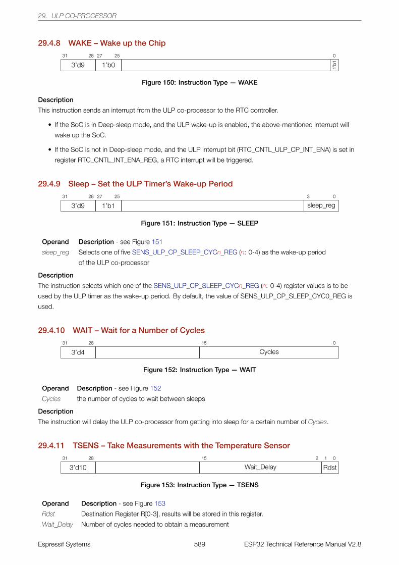
29. ULP CO-PROCESSOR
29.4.8 WAKE – Wake up the Chip025272831
3’d9 1’b0 1’b1
Figure 150: Instruction Type — WAKE
Description
This instruction sends an interrupt from the ULP co-processor to the RTC controller.
• If the SoC is in Deep-sleep mode, and the ULP wake-up is enabled, the above-mentioned interrupt will
wake up the SoC.
• If the SoC is not in Deep-sleep mode, and the ULP interrupt bit (RTC_CNTL_ULP_CP_INT_ENA) is set in
register RTC_CNTL_INT_ENA_REG, a RTC interrupt will be triggered.
29.4.9 Sleep – Set the ULP Timer’s Wake-up Period0325272831
3’d9 1’b1 sleep_reg
Figure 151: Instruction Type — SLEEP
Operand Description - see Figure 151
sleep_reg Selects one of five SENS_ULP_CP_SLEEP_CYCn_REG (n: 0-4) as the wake-up period
of the ULP co-processor
Description
The instruction selects which one of the SENS_ULP_CP_SLEEP_CYCn_REG (n: 0-4) register values is to be
used by the ULP timer as the wake-up period. By default, the value of SENS_ULP_CP_SLEEP_CYC0_REG is
used.
29.4.10 WAIT – Wait for a Number of Cycles0152831
3’d4 Cycles
Figure 152: Instruction Type — WAIT
Operand Description - see Figure 152
Cycles the number of cycles to wait between sleeps
Description
The instruction will delay the ULP co-processor from getting into sleep for a certain number of Cycles.
29.4.11 TSENS – Take Measurements with the Temperature Sensor012152831
3’d10 Wait_Delay Rdst
Figure 153: Instruction Type — TSENS
Operand Description - see Figure 153
Rdst Destination Register R[0-3], results will be stored in this register.
Wait_Delay Number of cycles needed to obtain a measurement
Espressif Systems 589 ESP32 Technical Reference Manual V2.8
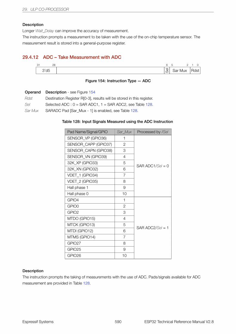
29. ULP CO-PROCESSOR
Description
Longer Wait_Delay can improve the accuracy of measurement.
The instruction prompts a measurement to be taken with the use of the on-chip temperature sensor. The
measurement result is stored into a general-purpose register.
29.4.12 ADC – Take Measurement with ADC
012562831
3’d5 Sel Sar Mux Rdst
Figure 154: Instruction Type — ADC
Operand Description - see Figure 154
Rdst Destination Register R[0-3], results will be stored in this register.
Sel Selected ADC : 0 = SAR ADC1, 1 = SAR ADC2, see Table 128.
Sar Mux SARADC Pad [Sar_Mux - 1] is enabled, see Table 128.
Table 128: Input Signals Measured using the ADC Instruction
Pad Name/Signal/GPIO Sar_Mux Processed by /Sel
SENSOR_VP (GPIO36) 1
SAR ADC1/Sel = 0
SENSOR_CAPP (GPIO37) 2
SENSOR_CAPN (GPIO38) 3
SENSOR_VN (GPIO39) 4
32K_XP (GPIO33) 5
32K_XN (GPIO32) 6
VDET_1 (GPIO34) 7
VDET_2 (GPIO35) 8
Hall phase 1 9
Hall phase 0 10
GPIO4 1
SAR ADC2/Sel = 1
GPIO0 2
GPIO2 3
MTDO (GPIO15) 4
MTCK (GPIO13) 5
MTDI (GPIO12) 6
MTMS (GPIO14) 7
GPIO27 8
GPIO25 9
GPIO26 10
Description
The instruction prompts the taking of measurements with the use of ADC. Pads/signals available for ADC
measurement are provided in Table 128.
Espressif Systems 590 ESP32 Technical Reference Manual V2.8
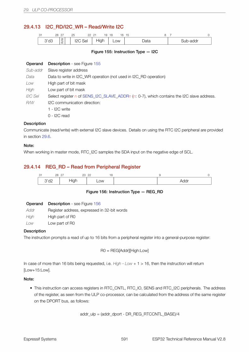
29. ULP CO-PROCESSOR
29.4.13 I2C_RD/I2C_WR – Read/Write I2C
07815161819212225272831
3’d3 R/W I2C Sel High Low Data Sub-addr
Figure 155: Instruction Type — I2C
Operand Description - see Figure 155
Sub-addr Slave register address
Data Data to write in I2C_WR operation (not used in I2C_RD operation)
Low High part of bit mask
High Low part of bit mask
I2C Sel Select register n of SENS_I2C_SLAVE_ADDRn (n: 0-7), which contains the I2C slave address.
R/W I2C communication direction:
1 - I2C write
0 - I2C read
Description
Communicate (read/write) with external I2C slave devices. Details on using the RTC I2C peripheral are provided
in section 29.6.
Note:
When working in master mode, RTC_I2C samples the SDA input on the negative edge of SCL.
29.4.14 REG_RD – Read from Peripheral Register
09182223272831
3’d2 High Low Addr
Figure 156: Instruction Type — REG_RD
Operand Description - see Figure 156
Addr Register address, expressed in 32-bit words
High High part of R0
Low Low part of R0
Description
The instruction prompts a read of up to 16 bits from a peripheral register into a general-purpose register:
R0 = REG[Addr][High:Low]
In case of more than 16 bits being requested, i.e. High - Low + 1 > 16, then the instruction will return
[Low+15:Low].
Note:
• This instruction can access registers in RTC_CNTL, RTC_IO, SENS and RTC_I2C peripherals. The address
of the register, as seen from the ULP co-processor, can be calculated from the address of the same register
on the DPORT bus, as follows:
addr_ulp = (addr_dport - DR_REG_RTCCNTL_BASE)/4
Espressif Systems 591 ESP32 Technical Reference Manual V2.8
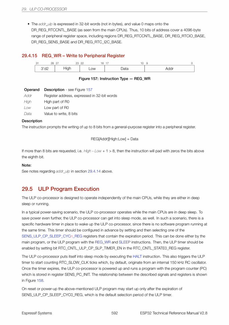
29. ULP CO-PROCESSOR
• The addr_ulp is expressed in 32-bit words (not in bytes), and value 0 maps onto the
DR_REG_RTCCNTL_BASE (as seen from the main CPUs). Thus, 10 bits of address cover a 4096-byte
range of peripheral register space, including regions DR_REG_RTCCNTL_BASE, DR_REG_RTCIO_BASE,
DR_REG_SENS_BASE and DR_REG_RTC_I2C_BASE.
29.4.15 REG_WR – Write to Peripheral Register
091017182223272831
3’d2 High Low Data Addr
Figure 157: Instruction Type — REG_WR
Operand Description - see Figure 157
Addr Register address, expressed in 32-bit words
High High part of R0
Low Low part of R0
Data Value to write, 8 bits
Description
The instruction prompts the writing of up to 8 bits from a general-purpose register into a peripheral register.
REG[Addr][High:Low] = Data
If more than 8 bits are requested, i.e. High - Low + 1 > 8, then the instruction will pad with zeros the bits above
the eighth bit.
Note:
See notes regarding addr_ulp in section 29.4.14 above.
29.5 ULP Program Execution
The ULP co-processor is designed to operate independently of the main CPUs, while they are either in deep
sleep or running.
In a typical power-saving scenario, the ULP co-processor operates while the main CPUs are in deep sleep. To
save power even further, the ULP co-processor can get into sleep mode, as well. In such a scenario, there is a
specific hardware timer in place to wake up the ULP co-processor, since there is no software program running at
the same time. This timer should be configured in advance by setting and then selecting one of the
SENS_ULP_CP_SLEEP_CYCn_REG registers that contain the expiration period. This can be done either by the
main program, or the ULP program with the REG_WR and SLEEP instructions. Then, the ULP timer should be
enabled by setting bit RTC_CNTL_ULP_CP_SLP_TIMER_EN in the RTC_CNTL_STATE0_REG register.
The ULP co-processor puts itself into sleep mode by executing the HALT instruction. This also triggers the ULP
timer to start counting RTC_SLOW_CLK ticks which, by default, originate from an internal 150 kHz RC oscillator.
Once the timer expires, the ULP co-processor is powered up and runs a program with the program counter (PC)
which is stored in register SENS_PC_INIT. The relationship between the described signals and registers is shown
in Figure 158.
On reset or power-up the above-mentioned ULP program may start up only after the expiration of
SENS_ULP_CP_SLEEP_CYC0_REG, which is the default selection period of the ULP timer.
Espressif Systems 592 ESP32 Technical Reference Manual V2.8
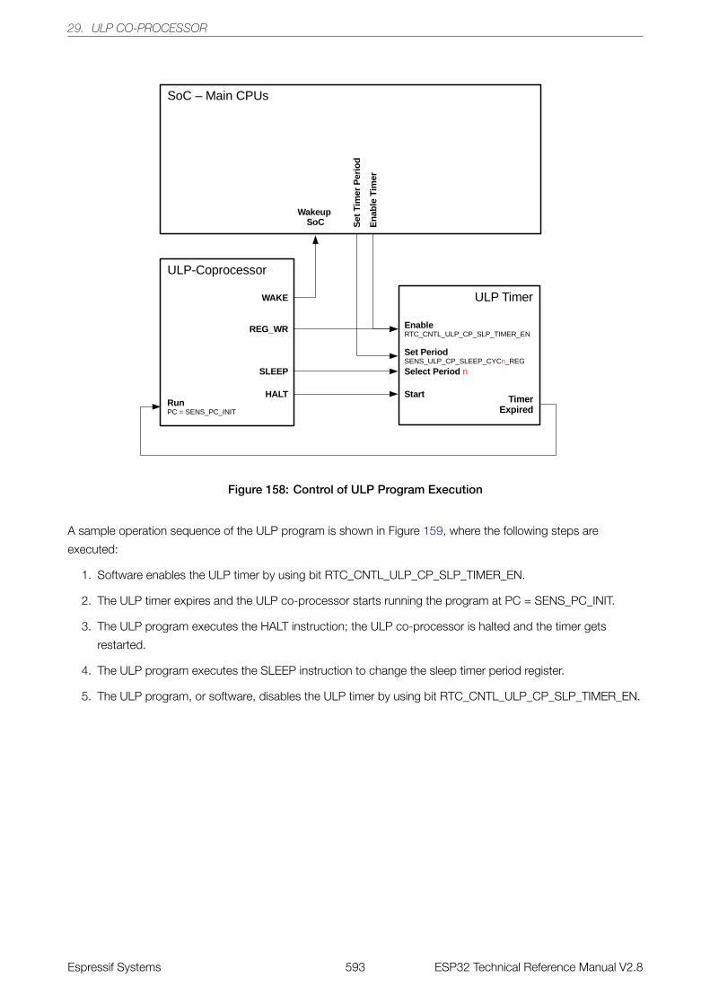
29. ULP CO-PROCESSOR
Figure 158: Control of ULP Program Execution
A sample operation sequence of the ULP program is shown in Figure 159, where the following steps are
executed:
1. Software enables the ULP timer by using bit RTC_CNTL_ULP_CP_SLP_TIMER_EN.
2. The ULP timer expires and the ULP co-processor starts running the program at PC = SENS_PC_INIT.
3. The ULP program executes the HALT instruction; the ULP co-processor is halted and the timer gets
restarted.
4. The ULP program executes the SLEEP instruction to change the sleep timer period register.
5. The ULP program, or software, disables the ULP timer by using bit RTC_CNTL_ULP_CP_SLP_TIMER_EN.
Espressif Systems 593 ESP32 Technical Reference Manual V2.8
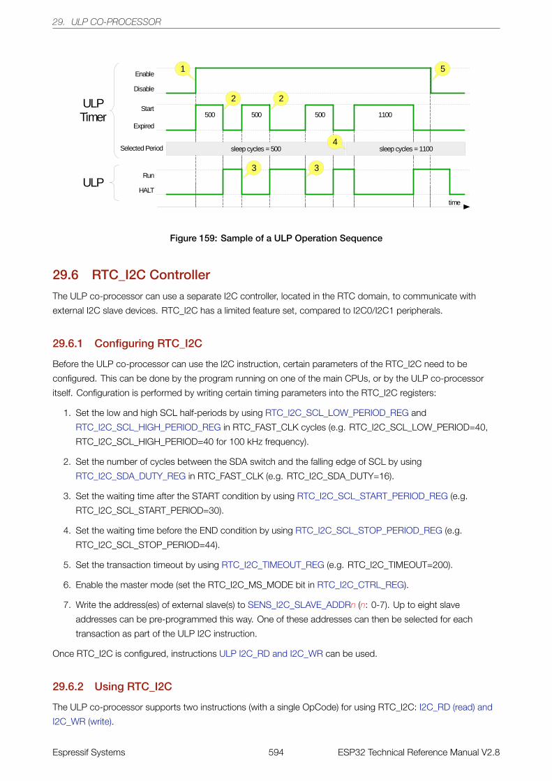
29. ULP CO-PROCESSOR
Figure 159: Sample of a ULP Operation Sequence
29.6 RTC_I2C Controller
The ULP co-processor can use a separate I2C controller, located in the RTC domain, to communicate with
external I2C slave devices. RTC_I2C has a limited feature set, compared to I2C0/I2C1 peripherals.
29.6.1 Configuring RTC_I2C
Before the ULP co-processor can use the I2C instruction, certain parameters of the RTC_I2C need to be
configured. This can be done by the program running on one of the main CPUs, or by the ULP co-processor
itself. Configuration is performed by writing certain timing parameters into the RTC_I2C registers:
1. Set the low and high SCL half-periods by using RTC_I2C_SCL_LOW_PERIOD_REG and
RTC_I2C_SCL_HIGH_PERIOD_REG in RTC_FAST_CLK cycles (e.g. RTC_I2C_SCL_LOW_PERIOD=40,
RTC_I2C_SCL_HIGH_PERIOD=40 for 100 kHz frequency).
2. Set the number of cycles between the SDA switch and the falling edge of SCL by using
RTC_I2C_SDA_DUTY_REG in RTC_FAST_CLK (e.g. RTC_I2C_SDA_DUTY=16).
3. Set the waiting time after the START condition by using RTC_I2C_SCL_START_PERIOD_REG (e.g.
RTC_I2C_SCL_START_PERIOD=30).
4. Set the waiting time before the END condition by using RTC_I2C_SCL_STOP_PERIOD_REG (e.g.
RTC_I2C_SCL_STOP_PERIOD=44).
5. Set the transaction timeout by using RTC_I2C_TIMEOUT_REG (e.g. RTC_I2C_TIMEOUT=200).
6. Enable the master mode (set the RTC_I2C_MS_MODE bit in RTC_I2C_CTRL_REG).
7. Write the address(es) of external slave(s) to SENS_I2C_SLAVE_ADDRn (n: 0-7). Up to eight slave
addresses can be pre-programmed this way. One of these addresses can then be selected for each
transaction as part of the ULP I2C instruction.
Once RTC_I2C is configured, instructions ULP I2C_RD and I2C_WR can be used.
29.6.2 Using RTC_I2C
The ULP co-processor supports two instructions (with a single OpCode) for using RTC_I2C: I2C_RD (read) and
I2C_WR (write).
Espressif Systems 594 ESP32 Technical Reference Manual V2.8
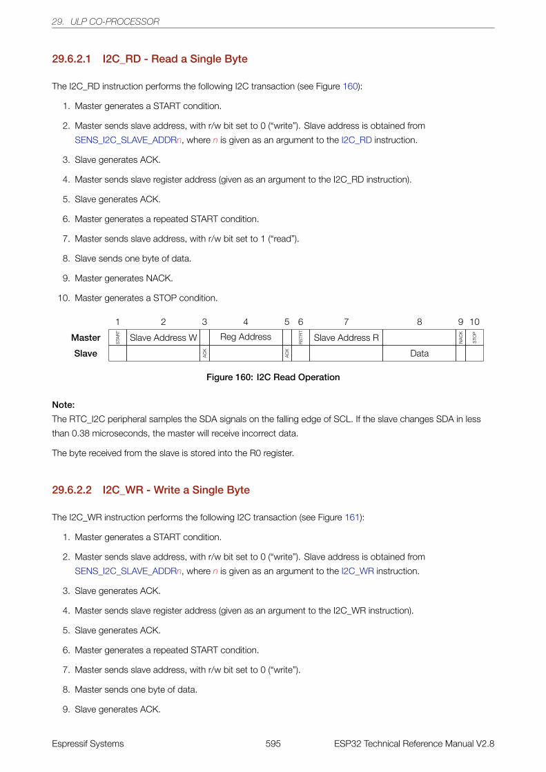
29. ULP CO-PROCESSOR
29.6.2.1 I2C_RD - Read a Single Byte
The I2C_RD instruction performs the following I2C transaction (see Figure 160):
1. Master generates a START condition.
2. Master sends slave address, with r/w bit set to 0 (“write”). Slave address is obtained from
SENS_I2C_SLAVE_ADDRn, where n is given as an argument to the I2C_RD instruction.
3. Slave generates ACK.
4. Master sends slave register address (given as an argument to the I2C_RD instruction).
5. Slave generates ACK.
6. Master generates a repeated START condition.
7. Master sends slave address, with r/w bit set to 1 (“read”).
8. Slave sends one byte of data.
9. Master generates NACK.
10. Master generates a STOP condition.
1 2 3 4 5 6 7 8 9 10
Master
STA
RT
Slave Address W Reg Address
RS
TRT
Slave Address R
NA
CK
STO
P
Slave AC
K
AC
K Data
Figure 160: I2C Read Operation
Note:
The RTC_I2C peripheral samples the SDA signals on the falling edge of SCL. If the slave changes SDA in less
than 0.38 microseconds, the master will receive incorrect data.
The byte received from the slave is stored into the R0 register.
29.6.2.2 I2C_WR - Write a Single Byte
The I2C_WR instruction performs the following I2C transaction (see Figure 161):
1. Master generates a START condition.
2. Master sends slave address, with r/w bit set to 0 (“write”). Slave address is obtained from
SENS_I2C_SLAVE_ADDRn, where n is given as an argument to the I2C_WR instruction.
3. Slave generates ACK.
4. Master sends slave register address (given as an argument to the I2C_WR instruction).
5. Slave generates ACK.
6. Master generates a repeated START condition.
7. Master sends slave address, with r/w bit set to 0 (“write”).
8. Master sends one byte of data.
9. Slave generates ACK.
Espressif Systems 595 ESP32 Technical Reference Manual V2.8
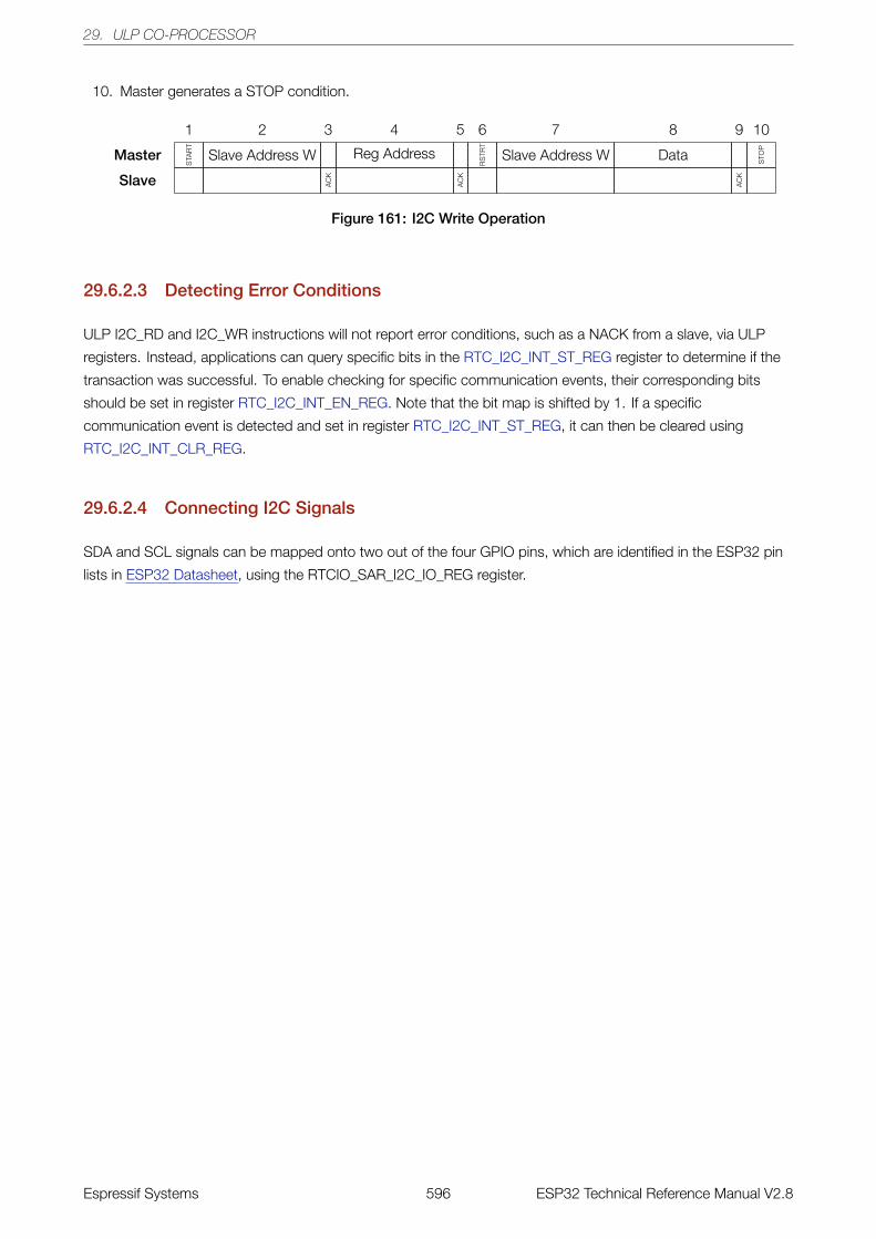
29. ULP CO-PROCESSOR
10. Master generates a STOP condition.
1 2 3 4 5 6 7 8 9 10
Master
STA
RT
Slave Address W Reg Address
RS
TRT
Slave Address W Data STO
P
Slave AC
K
AC
K
AC
K
Figure 161: I2C Write Operation
29.6.2.3 Detecting Error Conditions
ULP I2C_RD and I2C_WR instructions will not report error conditions, such as a NACK from a slave, via ULP
registers. Instead, applications can query specific bits in the RTC_I2C_INT_ST_REG register to determine if the
transaction was successful. To enable checking for specific communication events, their corresponding bits
should be set in register RTC_I2C_INT_EN_REG. Note that the bit map is shifted by 1. If a specific
communication event is detected and set in register RTC_I2C_INT_ST_REG, it can then be cleared using
RTC_I2C_INT_CLR_REG.
29.6.2.4 Connecting I2C Signals
SDA and SCL signals can be mapped onto two out of the four GPIO pins, which are identified in the ESP32 pin
lists in ESP32 Datasheet, using the RTCIO_SAR_I2C_IO_REG register.
Espressif Systems 596 ESP32 Technical Reference Manual V2.8
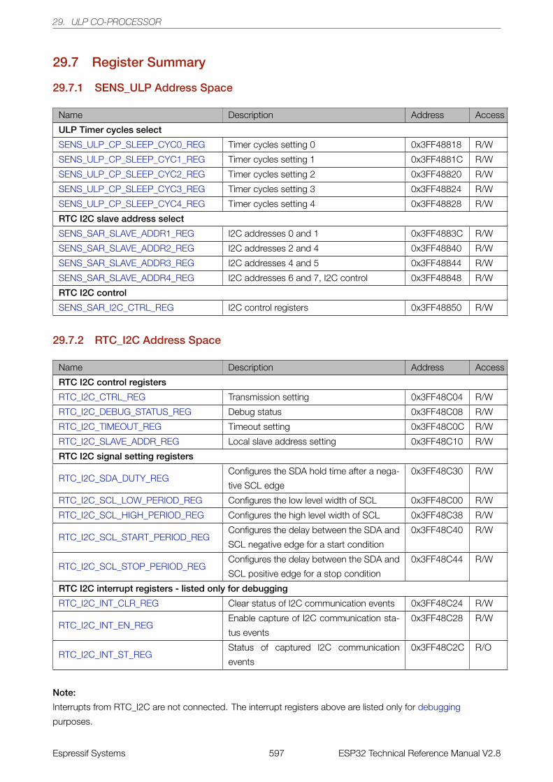
29. ULP CO-PROCESSOR
29.7 Register Summary
29.7.1 SENS_ULP Address Space
Name Description Address Access
ULP Timer cycles select
SENS_ULP_CP_SLEEP_CYC0_REG Timer cycles setting 0 0x3FF48818 R/W
SENS_ULP_CP_SLEEP_CYC1_REG Timer cycles setting 1 0x3FF4881C R/W
SENS_ULP_CP_SLEEP_CYC2_REG Timer cycles setting 2 0x3FF48820 R/W
SENS_ULP_CP_SLEEP_CYC3_REG Timer cycles setting 3 0x3FF48824 R/W
SENS_ULP_CP_SLEEP_CYC4_REG Timer cycles setting 4 0x3FF48828 R/W
RTC I2C slave address select
SENS_SAR_SLAVE_ADDR1_REG I2C addresses 0 and 1 0x3FF4883C R/W
SENS_SAR_SLAVE_ADDR2_REG I2C addresses 2 and 4 0x3FF48840 R/W
SENS_SAR_SLAVE_ADDR3_REG I2C addresses 4 and 5 0x3FF48844 R/W
SENS_SAR_SLAVE_ADDR4_REG I2C addresses 6 and 7, I2C control 0x3FF48848 R/W
RTC I2C control
SENS_SAR_I2C_CTRL_REG I2C control registers 0x3FF48850 R/W
29.7.2 RTC_I2C Address Space
Name Description Address Access
RTC I2C control registers
RTC_I2C_CTRL_REG Transmission setting 0x3FF48C04 R/W
RTC_I2C_DEBUG_STATUS_REG Debug status 0x3FF48C08 R/W
RTC_I2C_TIMEOUT_REG Timeout setting 0x3FF48C0C R/W
RTC_I2C_SLAVE_ADDR_REG Local slave address setting 0x3FF48C10 R/W
RTC I2C signal setting registers
RTC_I2C_SDA_DUTY_REGConfigures the SDA hold time after a nega-
tive SCL edge
0x3FF48C30 R/W
RTC_I2C_SCL_LOW_PERIOD_REG Configures the low level width of SCL 0x3FF48C00 R/W
RTC_I2C_SCL_HIGH_PERIOD_REG Configures the high level width of SCL 0x3FF48C38 R/W
RTC_I2C_SCL_START_PERIOD_REGConfigures the delay between the SDA and
SCL negative edge for a start condition
0x3FF48C40 R/W
RTC_I2C_SCL_STOP_PERIOD_REGConfigures the delay between the SDA and
SCL positive edge for a stop condition
0x3FF48C44 R/W
RTC I2C interrupt registers - listed only for debugging
RTC_I2C_INT_CLR_REG Clear status of I2C communication events 0x3FF48C24 R/W
RTC_I2C_INT_EN_REGEnable capture of I2C communication sta-
tus events
0x3FF48C28 R/W
RTC_I2C_INT_ST_REGStatus of captured I2C communication
events
0x3FF48C2C R/O
Note:
Interrupts from RTC_I2C are not connected. The interrupt registers above are listed only for debugging
purposes.
Espressif Systems 597 ESP32 Technical Reference Manual V2.8
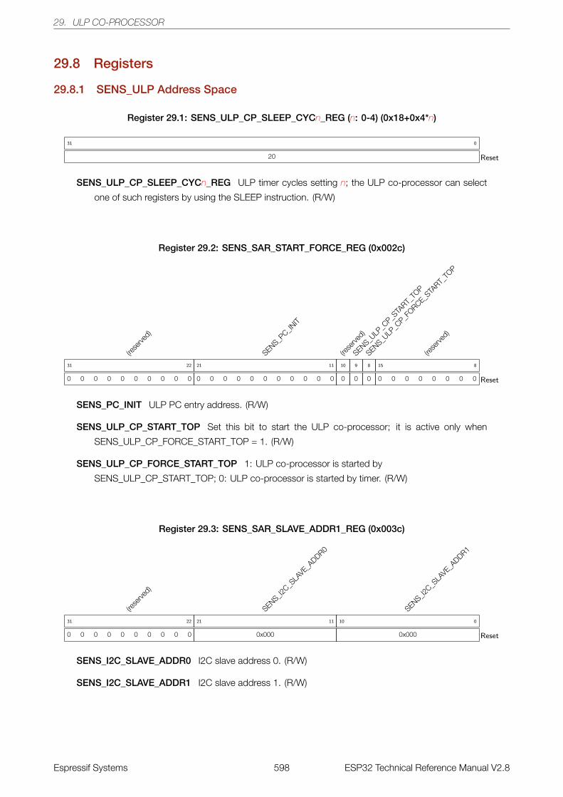
29. ULP CO-PROCESSOR
29.8 Registers
29.8.1 SENS_ULP Address Space
Register 29.1: SENS_ULP_CP_SLEEP_CYCn_REG (n: 0-4) (0x18+0x4*n)
20
31 0
Reset
SENS_ULP_CP_SLEEP_CYCn_REG ULP timer cycles setting n; the ULP co-processor can select
one of such registers by using the SLEEP instruction. (R/W)
Register 29.2: SENS_SAR_START_FORCE_REG (0x002c)
(rese
rved)
0 0 0 0 0 0 0 0 0 0
31 22
SENS_PC_IN
IT
0 0 0 0 0 0 0 0 0 0 0
21 11
(rese
rved)
0
10
SENS_ULP
_CP_S
TART_
TOP
0
9
SENS_ULP
_CP_F
ORCE_STA
RT_TO
P
0
8
(rese
rved)
0 0 0 0 0 0 0 0
15 8
Reset
SENS_PC_INIT ULP PC entry address. (R/W)
SENS_ULP_CP_START_TOP Set this bit to start the ULP co-processor; it is active only when
SENS_ULP_CP_FORCE_START_TOP = 1. (R/W)
SENS_ULP_CP_FORCE_START_TOP 1: ULP co-processor is started by
SENS_ULP_CP_START_TOP; 0: ULP co-processor is started by timer. (R/W)
Register 29.3: SENS_SAR_SLAVE_ADDR1_REG (0x003c)
(rese
rved)
0 0 0 0 0 0 0 0 0 0
31 22
SENS_I2C_S
LAVE_A
DDR0
0x000
21 11
SENS_I2C_S
LAVE_A
DDR1
0x000
10 0
Reset
SENS_I2C_SLAVE_ADDR0 I2C slave address 0. (R/W)
SENS_I2C_SLAVE_ADDR1 I2C slave address 1. (R/W)
Espressif Systems 598 ESP32 Technical Reference Manual V2.8
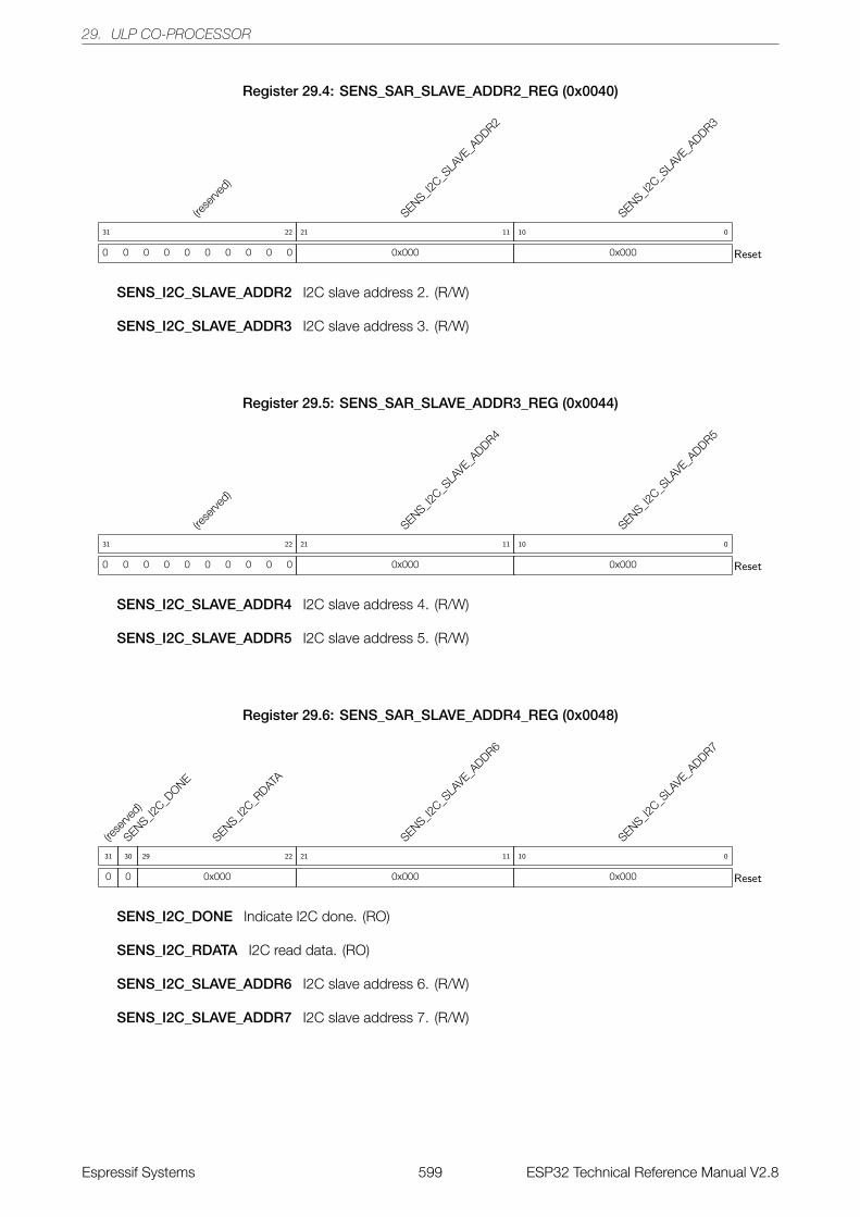
29. ULP CO-PROCESSOR
Register 29.4: SENS_SAR_SLAVE_ADDR2_REG (0x0040)
(rese
rved)
0 0 0 0 0 0 0 0 0 0
31 22
SENS_I2C_S
LAVE_A
DDR2
0x000
21 11
SENS_I2C_S
LAVE_A
DDR3
0x000
10 0
Reset
SENS_I2C_SLAVE_ADDR2 I2C slave address 2. (R/W)
SENS_I2C_SLAVE_ADDR3 I2C slave address 3. (R/W)
Register 29.5: SENS_SAR_SLAVE_ADDR3_REG (0x0044)
(rese
rved)
0 0 0 0 0 0 0 0 0 0
31 22
SENS_I2C_S
LAVE_A
DDR4
0x000
21 11
SENS_I2C_S
LAVE_A
DDR5
0x000
10 0
Reset
SENS_I2C_SLAVE_ADDR4 I2C slave address 4. (R/W)
SENS_I2C_SLAVE_ADDR5 I2C slave address 5. (R/W)
Register 29.6: SENS_SAR_SLAVE_ADDR4_REG (0x0048)
(rese
rved)
0
31
SENS_I2C_D
ONE
0
30
SENS_I2C_R
DATA
0x000
29 22
SENS_I2C_S
LAVE_A
DDR6
0x000
21 11
SENS_I2C_S
LAVE_A
DDR7
0x000
10 0
Reset
SENS_I2C_DONE Indicate I2C done. (RO)
SENS_I2C_RDATA I2C read data. (RO)
SENS_I2C_SLAVE_ADDR6 I2C slave address 6. (R/W)
SENS_I2C_SLAVE_ADDR7 I2C slave address 7. (R/W)
Espressif Systems 599 ESP32 Technical Reference Manual V2.8
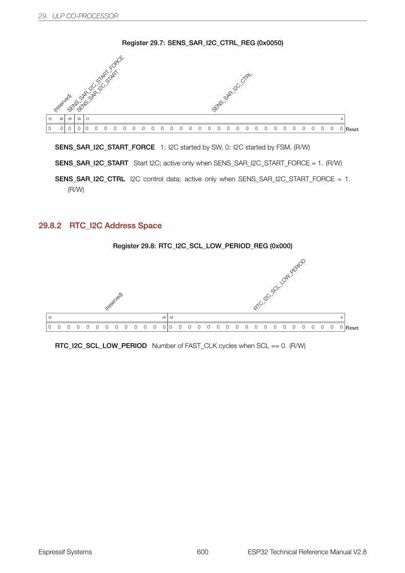
29. ULP CO-PROCESSOR
Register 29.7: SENS_SAR_I2C_CTRL_REG (0x0050)
(rese
rved)
0 0
31 30
SENS_SAR_I2
C_STA
RT_FO
RCE
0
29
SENS_SAR_I2
C_STA
RT
0
28
SENS_SAR_I2
C_CTR
L
0 0 0 0 0 0 0 0 0 0 0 0 0 0 0 0 0 0 0 0 0 0 0 0 0 0 0 0
27 0
Reset
SENS_SAR_I2C_START_FORCE 1: I2C started by SW, 0: I2C started by FSM. (R/W)
SENS_SAR_I2C_START Start I2C; active only when SENS_SAR_I2C_START_FORCE = 1. (R/W)
SENS_SAR_I2C_CTRL I2C control data; active only when SENS_SAR_I2C_START_FORCE = 1.
(R/W)
29.8.2 RTC_I2C Address Space
Register 29.8: RTC_I2C_SCL_LOW_PERIOD_REG (0x000)
(rese
rved)
0 0 0 0 0 0 0 0 0 0 0 0 0
31 19
RTC_I2
C_SCL_
LOW
_PERIO
D
0 0 0 0 0 0 0 0 0 0 0 0 0 0 0 0 0 0 0
18 0
Reset
RTC_I2C_SCL_LOW_PERIOD Number of FAST_CLK cycles when SCL == 0. (R/W)
Espressif Systems 600 ESP32 Technical Reference Manual V2.8
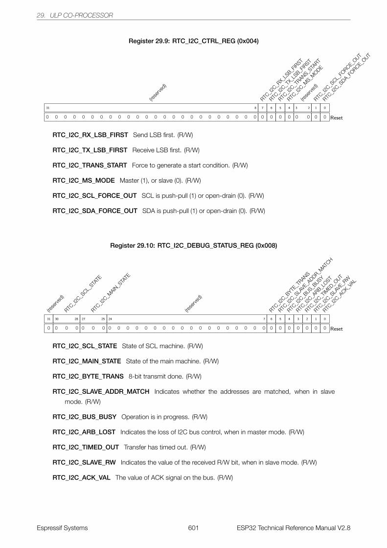
29. ULP CO-PROCESSOR
Register 29.9: RTC_I2C_CTRL_REG (0x004)
(rese
rved)
0 0 0 0 0 0 0 0 0 0 0 0 0 0 0 0 0 0 0 0 0 0 0 0
31 8
RTC_I2
C_RX_
LSB_F
IRST
0
7
RTC_I2
C_TX_
LSB_F
IRST
0
6
RTC_I2
C_TRANS_S
TART
0
5
RTC_I2
C_MS_M
ODE
0
4
(rese
rved)
0 0
3 2
RTC_I2
C_SCL_
FORCE_O
UT
0
1
RTC_I2
C_SDA_F
ORCE_OUT
0
0
Reset
RTC_I2C_RX_LSB_FIRST Send LSB first. (R/W)
RTC_I2C_TX_LSB_FIRST Receive LSB first. (R/W)
RTC_I2C_TRANS_START Force to generate a start condition. (R/W)
RTC_I2C_MS_MODE Master (1), or slave (0). (R/W)
RTC_I2C_SCL_FORCE_OUT SCL is push-pull (1) or open-drain (0). (R/W)
RTC_I2C_SDA_FORCE_OUT SDA is push-pull (1) or open-drain (0). (R/W)
Register 29.10: RTC_I2C_DEBUG_STATUS_REG (0x008)
(rese
rved)
0
31
RTC_I2
C_SCL_
STATE
0 0 0
30 28
RTC_I2
C_MAIN
_STA
TE
0 0 0
27 25
(rese
rved)
0 0 0 0 0 0 0 0 0 0 0 0 0 0 0 0 0 0
24 7
RTC_I2
C_BYTE
_TRANS
0
6
RTC_I2
C_SLA
VE_ADDR_M
ATCH
0
5
RTC_I2
C_BUS_B
USY
0
4
RTC_I2
C_ARB_L
OST
0
3
RTC_I2
C_TIM
ED_OUT
0
2
RTC_I2
C_SLA
VE_RW
0
1
RTC_I2
C_ACK_V
AL
0
0
Reset
RTC_I2C_SCL_STATE State of SCL machine. (R/W)
RTC_I2C_MAIN_STATE State of the main machine. (R/W)
RTC_I2C_BYTE_TRANS 8-bit transmit done. (R/W)
RTC_I2C_SLAVE_ADDR_MATCH Indicates whether the addresses are matched, when in slave
mode. (R/W)
RTC_I2C_BUS_BUSY Operation is in progress. (R/W)
RTC_I2C_ARB_LOST Indicates the loss of I2C bus control, when in master mode. (R/W)
RTC_I2C_TIMED_OUT Transfer has timed out. (R/W)
RTC_I2C_SLAVE_RW Indicates the value of the received R/W bit, when in slave mode. (R/W)
RTC_I2C_ACK_VAL The value of ACK signal on the bus. (R/W)
Espressif Systems 601 ESP32 Technical Reference Manual V2.8
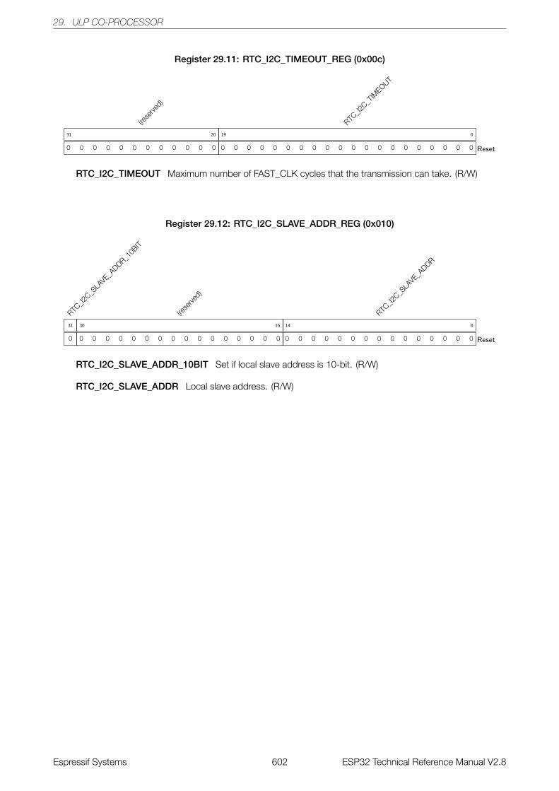
29. ULP CO-PROCESSOR
Register 29.11: RTC_I2C_TIMEOUT_REG (0x00c)
(rese
rved)
0 0 0 0 0 0 0 0 0 0 0 0
31 20
RTC_I2
C_TIM
EOUT
0 0 0 0 0 0 0 0 0 0 0 0 0 0 0 0 0 0 0 0
19 0
Reset
RTC_I2C_TIMEOUT Maximum number of FAST_CLK cycles that the transmission can take. (R/W)
Register 29.12: RTC_I2C_SLAVE_ADDR_REG (0x010)
RTC_I2
C_SLA
VE_ADDR_1
0BIT
0
31
(rese
rved)
0 0 0 0 0 0 0 0 0 0 0 0 0 0 0 0
30 15
RTC_I2
C_SLA
VE_ADDR
0 0 0 0 0 0 0 0 0 0 0 0 0 0 0
14 0
Reset
RTC_I2C_SLAVE_ADDR_10BIT Set if local slave address is 10-bit. (R/W)
RTC_I2C_SLAVE_ADDR Local slave address. (R/W)
Espressif Systems 602 ESP32 Technical Reference Manual V2.8
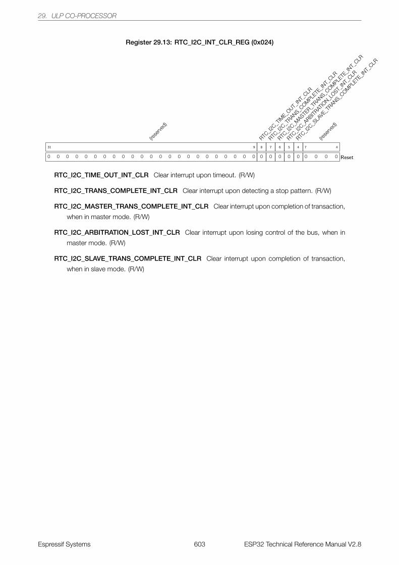
29. ULP CO-PROCESSOR
Register 29.13: RTC_I2C_INT_CLR_REG (0x024)
(rese
rved)
0 0 0 0 0 0 0 0 0 0 0 0 0 0 0 0 0 0 0 0 0 0 0
31 9
RTC_I2
C_TIM
E_OUT_
INT_
CLR
0
8
RTC_I2
C_TRANS_C
OMPLE
TE_IN
T_CLR
0
7
RTC_I2
C_MASTE
R_TRANS_C
OMPLE
TE_IN
T_CLR
0
6
RTC_I2
C_ARBITR
ATIO
N_LOST_
INT_
CLR
0
5
RTC_I2
C_SLA
VE_TRANS_C
OMPLE
TE_IN
T_CLR
0
4
(rese
rved)
0 0 0 0
7 4
Reset
RTC_I2C_TIME_OUT_INT_CLR Clear interrupt upon timeout. (R/W)
RTC_I2C_TRANS_COMPLETE_INT_CLR Clear interrupt upon detecting a stop pattern. (R/W)
RTC_I2C_MASTER_TRANS_COMPLETE_INT_CLR Clear interrupt upon completion of transaction,
when in master mode. (R/W)
RTC_I2C_ARBITRATION_LOST_INT_CLR Clear interrupt upon losing control of the bus, when in
master mode. (R/W)
RTC_I2C_SLAVE_TRANS_COMPLETE_INT_CLR Clear interrupt upon completion of transaction,
when in slave mode. (R/W)
Espressif Systems 603 ESP32 Technical Reference Manual V2.8
29. ULP CO-PROCESSOR
Register 29.14: RTC_I2C_INT_EN_REG (0x028)
(rese
rved)
0 0 0 0 0 0 0 0 0 0 0 0 0 0 0 0 0 0 0 0 0 0 0
31 9
RTC_I2
C_TIM
E_OUT_
INT_
ENA
0
8
RTC_I2
C_TRANS_C
OMPLE
TE_IN
T_ENA
0
7
RTC_I2
C_MASTE
R_TRAN_C
OMP_IN
T_ENA
0
6
RTC_I2
C_ARBITR
ATIO
N_LOST_
INT_
ENA
0
5
RTC_I2
C_SLA
VE_TRAN_C
OMP_IN
T_ENA
0
4
(rese
rved)
0 0 0 0
7 4
Reset
RTC_I2C_TIME_OUT_INT_ENA Enable interrupt upon timeout. (R/W)
RTC_I2C_TRANS_COMPLETE_INT_ENA Enable interrupt upon detecting a stop pattern. (R/W)
RTC_I2C_MASTER_TRAN_COMP_INT_ENA Enable interrupt upon completion of transaction,
when in master mode. (R/W)
RTC_I2C_ARBITRATION_LOST_INT_ENA Enable interrupt upon losing control of the bus, when in
master mode. (R/W)
RTC_I2C_SLAVE_TRAN_COMP_INT_ENA Enable interrupt upon completion of transaction, when
in slave mode. (R/W)
Register 29.15: RTC_I2C_INT_ST_REG (0x02c)
(rese
rved)
0 0 0 0 0 0 0 0 0 0 0 0 0 0 0 0 0 0 0 0 0 0 0 0
31 8
RTC_I2
C_TIM
E_OUT_
INT_
ST
0
7
RTC_I2
C_TRANS_C
OMPLE
TE_IN
T_ST
0
6
RTC_I2
C_MASTE
R_TRAN_C
OMP_IN
T_ST
0
5
RTC_I2
C_ARBITR
ATIO
N_LOST_
INT_
ST
0
4
RTC_I2
C_SLA
VE_TRAN_C
OMP_IN
T_ST
0
3
(rese
rved)
0 0 0
5 3
Reset
RTC_I2C_TIME_OUT_INT_ST Detected timeout. (R/O)
RTC_I2C_TRANS_COMPLETE_INT_ST Detected stop pattern on I2C bus. (R/O)
RTC_I2C_MASTER_TRAN_COMP_INT_ST Transaction completed, when in master mode. (R/O)
RTC_I2C_ARBITRATION_LOST_INT_ST Bus control lost, when in master mode. (R/O)
RTC_I2C_SLAVE_TRAN_COMP_INT_ST Transaction completed, when in slave mode. (R/O)
Espressif Systems 604 ESP32 Technical Reference Manual V2.8
29. ULP CO-PROCESSOR
Register 29.16: RTC_I2C_SDA_DUTY_REG (0x030)
(rese
rved)
0 0 0 0 0 0 0 0 0 0 0 0
31 20
RTC_I2
C_SDA_D
UTY
0 0 0 0 0 0 0 0 0 0 0 0 0 0 0 0 0 0 0 0
19 0
Reset
RTC_I2C_SDA_DUTY Number of FAST_CLK cycles between the SDA switch and the falling edge of
SCL. (R/W)
Register 29.17: RTC_I2C_SCL_HIGH_PERIOD_REG (0x038)
(rese
rved)
0 0 0 0 0 0 0 0 0 0 0 0
31 20
RTC_I2
C_SCL_
HIGH_P
ERIOD
0 0 0 0 0 0 0 0 0 0 0 0 0 0 0 0 0 0 0 0
19 0
Reset
RTC_I2C_SCL_HIGH_PERIOD Number of FAST_CLK cycles when SCL == 1. (R/W)
Register 29.18: RTC_I2C_SCL_START_PERIOD_REG (0x040)
(rese
rved)
0 0 0 0 0 0 0 0 0 0 0 0
31 20
RTC_I2
C_SCL_
START_
PERIOD
0 0 0 0 0 0 0 0 0 0 0 0 0 0 0 0 0 0 0 0
19 0
Reset
RTC_I2C_SCL_START_PERIOD Number of FAST_CLK cycles to wait before generating a start con-
dition. (R/W)
Espressif Systems 605 ESP32 Technical Reference Manual V2.8
29. ULP CO-PROCESSOR
Register 29.19: RTC_I2C_SCL_STOP_PERIOD_REG (0x044)
(rese
rved)
0 0 0 0 0 0 0 0 0 0 0 0
31 20
RTC_I2
C_SCL_
STOP_P
ERIOD
0 0 0 0 0 0 0 0 0 0 0 0 0 0 0 0 0 0 0 0
19 0
Reset
RTC_I2C_SCL_STOP_PERIOD Number of FAST_CLK cycles to wait before generating a stop con-
dition. (R/W)
Espressif Systems 606 ESP32 Technical Reference Manual V2.8
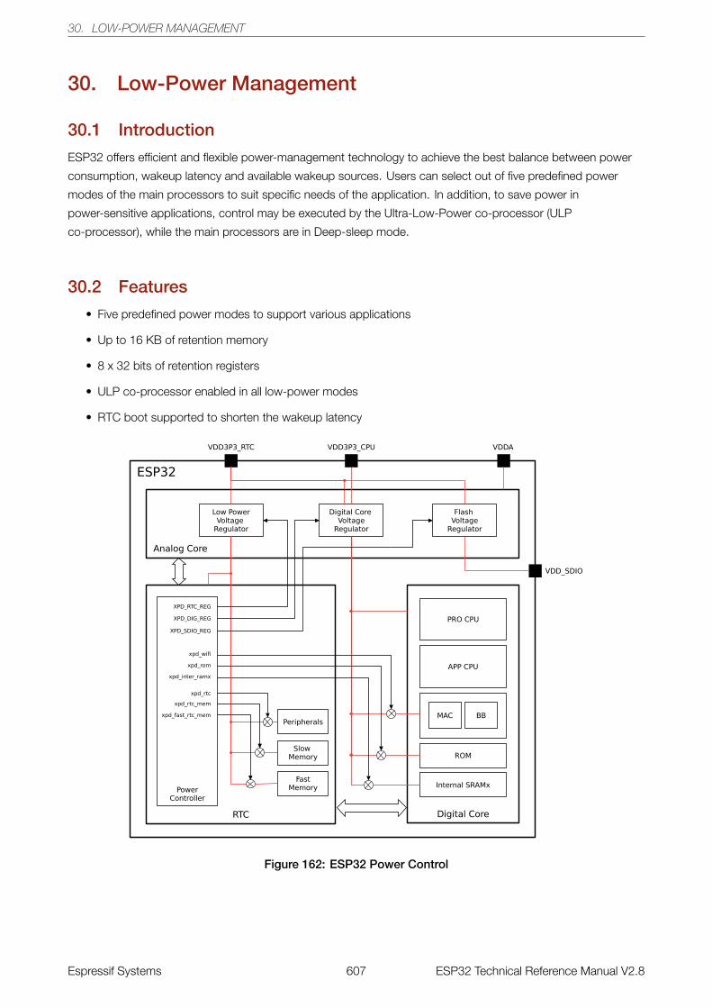
30. LOW-POWER MANAGEMENT
30. Low-Power Management
30.1 Introduction
ESP32 offers efficient and flexible power-management technology to achieve the best balance between power
consumption, wakeup latency and available wakeup sources. Users can select out of five predefined power
modes of the main processors to suit specific needs of the application. In addition, to save power in
power-sensitive applications, control may be executed by the Ultra-Low-Power co-processor (ULP
co-processor), while the main processors are in Deep-sleep mode.
30.2 Features
• Five predefined power modes to support various applications
• Up to 16 KB of retention memory
• 8 x 32 bits of retention registers
• ULP co-processor enabled in all low-power modes
• RTC boot supported to shorten the wakeup latency
Figure 162: ESP32 Power Control
Espressif Systems 607 ESP32 Technical Reference Manual V2.8
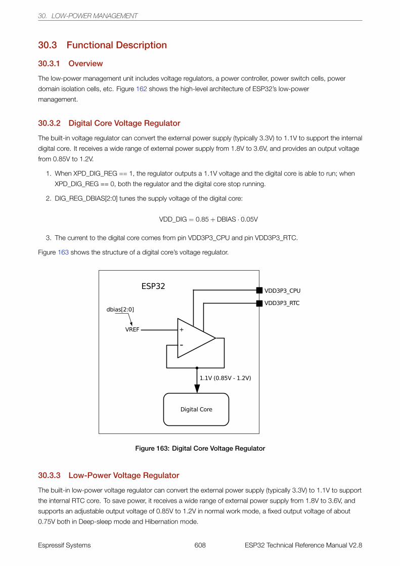
30. LOW-POWER MANAGEMENT
30.3 Functional Description
30.3.1 Overview
The low-power management unit includes voltage regulators, a power controller, power switch cells, power
domain isolation cells, etc. Figure 162 shows the high-level architecture of ESP32’s low-power
management.
30.3.2 Digital Core Voltage Regulator
The built-in voltage regulator can convert the external power supply (typically 3.3V) to 1.1V to support the internal
digital core. It receives a wide range of external power supply from 1.8V to 3.6V, and provides an output voltage
from 0.85V to 1.2V.
1. When XPD_DIG_REG == 1, the regulator outputs a 1.1V voltage and the digital core is able to run; when
XPD_DIG_REG == 0, both the regulator and the digital core stop running.
2. DIG_REG_DBIAS[2:0] tunes the supply voltage of the digital core:
VDD_DIG = 0.85 + DBIAS · 0.05V
3. The current to the digital core comes from pin VDD3P3_CPU and pin VDD3P3_RTC.
Figure 163 shows the structure of a digital core’s voltage regulator.
Figure 163: Digital Core Voltage Regulator
30.3.3 Low-Power Voltage Regulator
The built-in low-power voltage regulator can convert the external power supply (typically 3.3V) to 1.1V to support
the internal RTC core. To save power, it receives a wide range of external power supply from 1.8V to 3.6V, and
supports an adjustable output voltage of 0.85V to 1.2V in normal work mode, a fixed output voltage of about
0.75V both in Deep-sleep mode and Hibernation mode.
Espressif Systems 608 ESP32 Technical Reference Manual V2.8
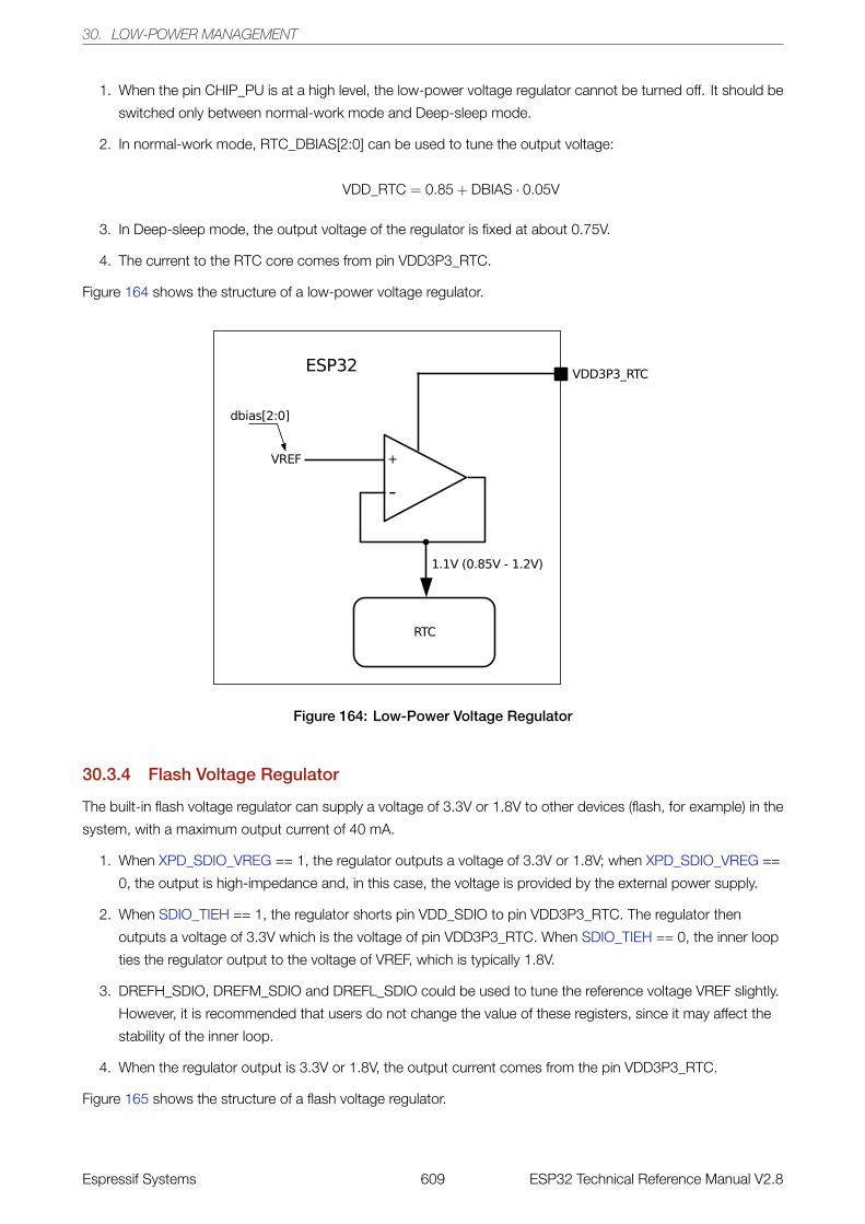
30. LOW-POWER MANAGEMENT
1. When the pin CHIP_PU is at a high level, the low-power voltage regulator cannot be turned off. It should be
switched only between normal-work mode and Deep-sleep mode.
2. In normal-work mode, RTC_DBIAS[2:0] can be used to tune the output voltage:
VDD_RTC = 0.85 + DBIAS · 0.05V
3. In Deep-sleep mode, the output voltage of the regulator is fixed at about 0.75V.
4. The current to the RTC core comes from pin VDD3P3_RTC.
Figure 164 shows the structure of a low-power voltage regulator.
Figure 164: Low-Power Voltage Regulator
30.3.4 Flash Voltage Regulator
The built-in flash voltage regulator can supply a voltage of 3.3V or 1.8V to other devices (flash, for example) in the
system, with a maximum output current of 40 mA.
1. When XPD_SDIO_VREG == 1, the regulator outputs a voltage of 3.3V or 1.8V; when XPD_SDIO_VREG ==
0, the output is high-impedance and, in this case, the voltage is provided by the external power supply.
2. When SDIO_TIEH == 1, the regulator shorts pin VDD_SDIO to pin VDD3P3_RTC. The regulator then
outputs a voltage of 3.3V which is the voltage of pin VDD3P3_RTC. When SDIO_TIEH == 0, the inner loop
ties the regulator output to the voltage of VREF, which is typically 1.8V.
3. DREFH_SDIO, DREFM_SDIO and DREFL_SDIO could be used to tune the reference voltage VREF slightly.
However, it is recommended that users do not change the value of these registers, since it may affect the
stability of the inner loop.
4. When the regulator output is 3.3V or 1.8V, the output current comes from the pin VDD3P3_RTC.
Figure 165 shows the structure of a flash voltage regulator.
Espressif Systems 609 ESP32 Technical Reference Manual V2.8
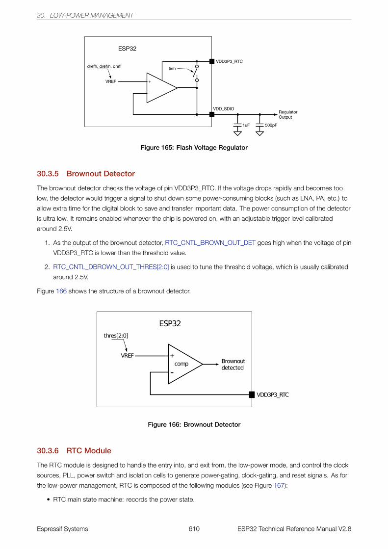
30. LOW-POWER MANAGEMENT
Figure 165: Flash Voltage Regulator
30.3.5 Brownout Detector
The brownout detector checks the voltage of pin VDD3P3_RTC. If the voltage drops rapidly and becomes too
low, the detector would trigger a signal to shut down some power-consuming blocks (such as LNA, PA, etc.) to
allow extra time for the digital block to save and transfer important data. The power consumption of the detector
is ultra low. It remains enabled whenever the chip is powered on, with an adjustable trigger level calibrated
around 2.5V.
1. As the output of the brownout detector, RTC_CNTL_BROWN_OUT_DET goes high when the voltage of pin
VDD3P3_RTC is lower than the threshold value.
2. RTC_CNTL_DBROWN_OUT_THRES[2:0] is used to tune the threshold voltage, which is usually calibrated
around 2.5V.
Figure 166 shows the structure of a brownout detector.
Figure 166: Brownout Detector
30.3.6 RTC Module
The RTC module is designed to handle the entry into, and exit from, the low-power mode, and control the clock
sources, PLL, power switch and isolation cells to generate power-gating, clock-gating, and reset signals. As for
the low-power management, RTC is composed of the following modules (see Figure 167):
• RTC main state machine: records the power state.
Espressif Systems 610 ESP32 Technical Reference Manual V2.8
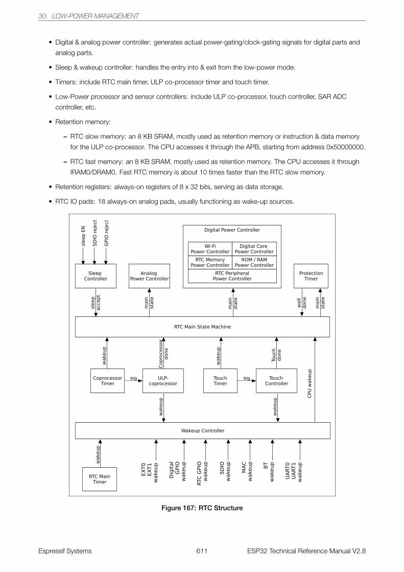
30. LOW-POWER MANAGEMENT
• Digital & analog power controller: generates actual power-gating/clock-gating signals for digital parts and
analog parts.
• Sleep & wakeup controller: handles the entry into & exit from the low-power mode.
• Timers: include RTC main timer, ULP co-processor timer and touch timer.
• Low-Power processor and sensor controllers: include ULP co-processor, touch controller, SAR ADC
controller, etc.
• Retention memory:
– RTC slow memory: an 8 KB SRAM, mostly used as retention memory or instruction & data memory
for the ULP co-processor. The CPU accesses it through the APB, starting from address 0x50000000.
– RTC fast memory: an 8 KB SRAM, mostly used as retention memory. The CPU accesses it through
IRAM0/DRAM0. Fast RTC memory is about 10 times faster than the RTC slow memory.
• Retention registers: always-on registers of 8 x 32 bits, serving as data storage.
• RTC IO pads: 18 always-on analog pads, usually functioning as wake-up sources.
Figure 167: RTC Structure
Espressif Systems 611 ESP32 Technical Reference Manual V2.8
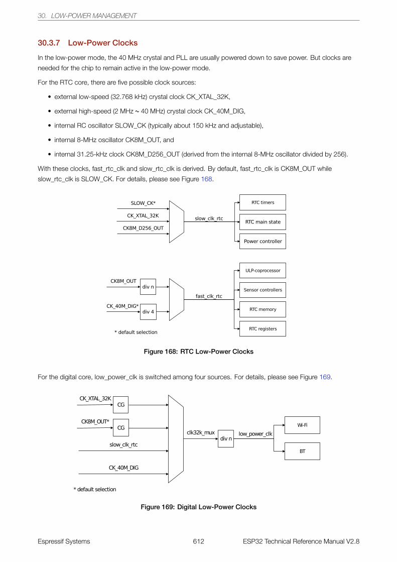
30. LOW-POWER MANAGEMENT
30.3.7 Low-Power Clocks
In the low-power mode, the 40 MHz crystal and PLL are usually powered down to save power. But clocks are
needed for the chip to remain active in the low-power mode.
For the RTC core, there are five possible clock sources:
• external low-speed (32.768 kHz) crystal clock CK_XTAL_32K,
• external high-speed (2 MHz ~ 40 MHz) crystal clock CK_40M_DIG,
• internal RC oscillator SLOW_CK (typically about 150 kHz and adjustable),
• internal 8-MHz oscillator CK8M_OUT, and
• internal 31.25-kHz clock CK8M_D256_OUT (derived from the internal 8-MHz oscillator divided by 256).
With these clocks, fast_rtc_clk and slow_rtc_clk is derived. By default, fast_rtc_clk is CK8M_OUT while
slow_rtc_clk is SLOW_CK. For details, please see Figure 168.
Figure 168: RTC Low-Power Clocks
For the digital core, low_power_clk is switched among four sources. For details, please see Figure 169.
Figure 169: Digital Low-Power Clocks
Espressif Systems 612 ESP32 Technical Reference Manual V2.8
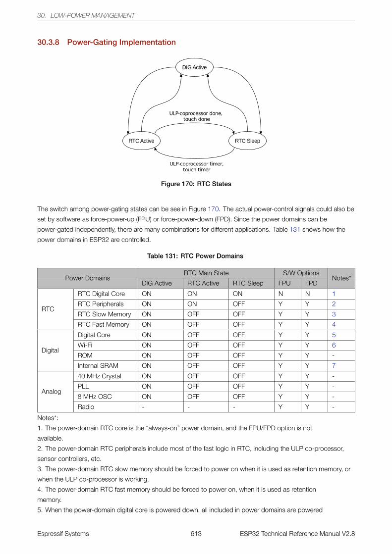
30. LOW-POWER MANAGEMENT
30.3.8 Power-Gating Implementation
Figure 170: RTC States
The switch among power-gating states can be see in Figure 170. The actual power-control signals could also be
set by software as force-power-up (FPU) or force-power-down (FPD). Since the power domains can be
power-gated independently, there are many combinations for different applications. Table 131 shows how the
power domains in ESP32 are controlled.
Table 131: RTC Power Domains
RTC Main State S/W OptionsPower Domains
DIG Active RTC Active RTC Sleep FPU FPDNotes*
RTC
RTC Digital Core ON ON ON N N 1
RTC Peripherals ON ON OFF Y Y 2
RTC Slow Memory ON OFF OFF Y Y 3
RTC Fast Memory ON OFF OFF Y Y 4
Digital
Digital Core ON OFF OFF Y Y 5
Wi-Fi ON OFF OFF Y Y 6
ROM ON OFF OFF Y Y -
Internal SRAM ON OFF OFF Y Y 7
Analog
40 MHz Crystal ON OFF OFF Y Y -
PLL ON OFF OFF Y Y -
8 MHz OSC ON OFF OFF Y Y -
Radio - - - Y Y -
Notes*:
1. The power-domain RTC core is the “always-on” power domain, and the FPU/FPD option is not
available.
2. The power-domain RTC peripherals include most of the fast logic in RTC, including the ULP co-processor,
sensor controllers, etc.
3. The power-domain RTC slow memory should be forced to power on when it is used as retention memory, or
when the ULP co-processor is working.
4. The power-domain RTC fast memory should be forced to power on, when it is used as retention
memory.
5. When the power-domain digital core is powered down, all included in power domains are powered
Espressif Systems 613 ESP32 Technical Reference Manual V2.8
30. LOW-POWER MANAGEMENT
down.
6. The power-domain Wi-Fi includes the Wi-Fi MAC and BB.
7. Each internal SRAM can be power-gated independently.
30.3.9 Predefined Power Modes
In ESP32, we recommend that you always use the predefined power modes first, before trying to tune each
power control signal. The predefined power modes should cover most scenarios:
• Active mode
– The CPU is clocked at XTAL_DIV_N (40 MHz/26 MHz) or PLL (80 MHz/160 MHz/240 MHz).
– The chip can receive, transmit, or listen.
• Modem-sleep mode
– The CPU is operational and the clock is configurable.
– The Wi-Fi/Bluetooth baseband is clock-gated or powered down. The radio is turned off.
– Current consumption: ∼30 mA with 80 MHz PLL.
– Current consumption: ∼3 mA with 2 MHz XTAL.
– Immediate wake-up.
• Light-sleep mode
– The internal 8 MHz oscillator, 40 MHz high-speed crystal, PLL, and radio are disabled.
– The clock in the digital core is gated. The CPUs are stalled.
– The ULP co-processor and touch controller can be periodically triggered by monitor sensors.
– Current consumption: ∼ 800 µA.
– Wake-up latency: less than 1 ms.
• Deep-sleep mode
– The internal 8 MHz oscillator, 40 MHz high-speed crystal, PLL and radio are disabled.
– The digital core is powered down. The CPU context is lost.
– The supply voltage to the RTC core drops to 0.7V.
– 8 x 32 bits of data are kept in general-purpose retention registers.
– The RTC memory and fast RTC memory can be retained.
– Current consumption: ∼ 6.5 µA.
– Wake-up latency: less than 1 ms.
– Recommended for ultra-low-power infrequently-connected Wi-Fi/Bluetooth applications.
• Hibernatation mode
– The internal 8 MHz oscillator, 40 MHz high-speed crystal, PLL, and radio are disabled.
– The digital core is powered down. The CPU context is lost.
– The RTC peripheral domain is powered down.
Espressif Systems 614 ESP32 Technical Reference Manual V2.8
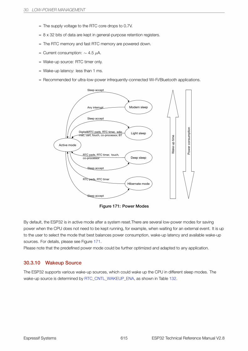
30. LOW-POWER MANAGEMENT
– The supply voltage to the RTC core drops to 0.7V.
– 8 x 32 bits of data are kept in general-purpose retention registers.
– The RTC memory and fast RTC memory are powered down.
– Current consumption: ∼ 4.5 µA.
– Wake-up source: RTC timer only.
– Wake-up latency: less than 1 ms.
– Recommended for ultra-low-power infrequently-connected Wi-Fi/Bluetooth applications.
Figure 171: Power Modes
By default, the ESP32 is in active mode after a system reset.There are several low-power modes for saving
power when the CPU does not need to be kept running, for example, when waiting for an external event. It is up
to the user to select the mode that best balances power consumption, wake-up latency and available wake-up
sources. For details, please see Figure 171.
Please note that the predefined power mode could be further optimized and adapted to any application.
30.3.10 Wakeup Source
The ESP32 supports various wake-up sources, which could wake up the CPU in different sleep modes. The
wake-up source is determined by RTC_CNTL_WAKEUP_ENA, as shown in Table 132.
Espressif Systems 615 ESP32 Technical Reference Manual V2.8
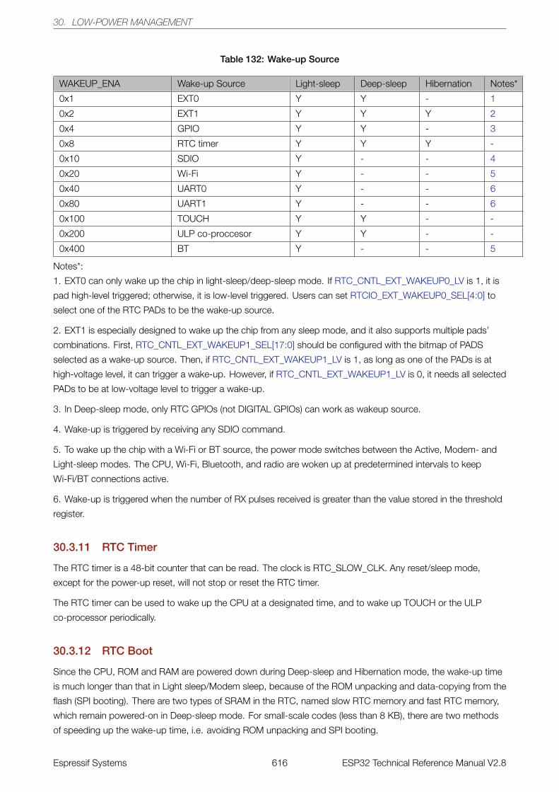
30. LOW-POWER MANAGEMENT
Table 132: Wake-up Source
WAKEUP_ENA Wake-up Source Light-sleep Deep-sleep Hibernation Notes*
0x1 EXT0 Y Y - 1
0x2 EXT1 Y Y Y 2
0x4 GPIO Y Y - 3
0x8 RTC timer Y Y Y -
0x10 SDIO Y - - 4
0x20 Wi-Fi Y - - 5
0x40 UART0 Y - - 6
0x80 UART1 Y - - 6
0x100 TOUCH Y Y - -
0x200 ULP co-proccesor Y Y - -
0x400 BT Y - - 5
Notes*:
1. EXT0 can only wake up the chip in light-sleep/deep-sleep mode. If RTC_CNTL_EXT_WAKEUP0_LV is 1, it is
pad high-level triggered; otherwise, it is low-level triggered. Users can set RTCIO_EXT_WAKEUP0_SEL[4:0] to
select one of the RTC PADs to be the wake-up source.
2. EXT1 is especially designed to wake up the chip from any sleep mode, and it also supports multiple pads’
combinations. First, RTC_CNTL_EXT_WAKEUP1_SEL[17:0] should be configured with the bitmap of PADS
selected as a wake-up source. Then, if RTC_CNTL_EXT_WAKEUP1_LV is 1, as long as one of the PADs is at
high-voltage level, it can trigger a wake-up. However, if RTC_CNTL_EXT_WAKEUP1_LV is 0, it needs all selected
PADs to be at low-voltage level to trigger a wake-up.
3. In Deep-sleep mode, only RTC GPIOs (not DIGITAL GPIOs) can work as wakeup source.
4. Wake-up is triggered by receiving any SDIO command.
5. To wake up the chip with a Wi-Fi or BT source, the power mode switches between the Active, Modem- and
Light-sleep modes. The CPU, Wi-Fi, Bluetooth, and radio are woken up at predetermined intervals to keep
Wi-Fi/BT connections active.
6. Wake-up is triggered when the number of RX pulses received is greater than the value stored in the threshold
register.
30.3.11 RTC Timer
The RTC timer is a 48-bit counter that can be read. The clock is RTC_SLOW_CLK. Any reset/sleep mode,
except for the power-up reset, will not stop or reset the RTC timer.
The RTC timer can be used to wake up the CPU at a designated time, and to wake up TOUCH or the ULP
co-processor periodically.
30.3.12 RTC Boot
Since the CPU, ROM and RAM are powered down during Deep-sleep and Hibernation mode, the wake-up time
is much longer than that in Light sleep/Modem sleep, because of the ROM unpacking and data-copying from the
flash (SPI booting). There are two types of SRAM in the RTC, named slow RTC memory and fast RTC memory,
which remain powered-on in Deep-sleep mode. For small-scale codes (less than 8 KB), there are two methods
of speeding up the wake-up time, i.e. avoiding ROM unpacking and SPI booting.
Espressif Systems 616 ESP32 Technical Reference Manual V2.8
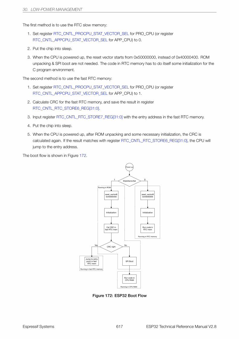
30. LOW-POWER MANAGEMENT
The first method is to use the RTC slow memory:
1. Set register RTC_CNTL_PROCPU_STAT_VECTOR_SEL for PRO_CPU (or register
RTC_CNTL_APPCPU_STAT_VECTOR_SEL for APP_CPU) to 0.
2. Put the chip into sleep.
3. When the CPU is powered up, the reset vector starts from 0x50000000, instead of 0x40000400. ROM
unpacking & SPI boot are not needed. The code in RTC memory has to do itself some initialization for the
C program environment.
The second method is to use the fast RTC memory:
1. Set register RTC_CNTL_PROCPU_STAT_VECTOR_SEL for PRO_CPU (or register
RTC_CNTL_APPCPU_STAT_VECTOR_SEL for APP_CPU) to 1.
2. Calculate CRC for the fast RTC memory, and save the result in register
RTC_CNTL_RTC_STORE6_REG[31:0].
3. Input register RTC_CNTL_RTC_STORE7_REG[31:0] with the entry address in the fast RTC memory.
4. Put the chip into sleep.
5. When the CPU is powered up, after ROM unpacking and some necessary initialization, the CRC is
calculated again. If the result matches with register RTC_CNTL_RTC_STORE6_REG[31:0], the CPU will
jump to the entry address.
The boot flow is shown in Figure 172.
Figure 172: ESP32 Boot Flow
Espressif Systems 617 ESP32 Technical Reference Manual V2.8
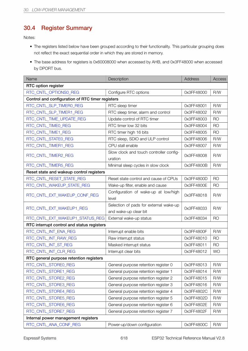
30. LOW-POWER MANAGEMENT
30.4 Register Summary
Notes:
• The registers listed below have been grouped according to their functionality. This particular grouping does
not reflect the exact sequential order in which they are stored in memory.
• The base address for registers is 0x60008000 when accessed by AHB, and 0x3FF48000 when accessed
by DPORT bus.
Name Description Address Access
RTC option register
RTC_CNTL_OPTIONS0_REG Configure RTC options 0x3FF48000 R/W
Control and configuration of RTC timer registers
RTC_CNTL_SLP_TIMER0_REG RTC sleep timer 0x3FF48001 R/W
RTC_CNTL_SLP_TIMER1_REG RTC sleep timer, alarm and control 0x3FF48002 R/W
RTC_CNTL_TIME_UPDATE_REG Update control of RTC timer 0x3FF48003 RO
RTC_CNTL_TIME0_REG RTC timer low 32 bits 0x3FF48004 RO
RTC_CNTL_TIME1_REG RTC timer high 16 bits 0x3FF48005 RO
RTC_CNTL_STATE0_REG RTC sleep, SDIO and ULP control 0x3FF48006 R/W
RTC_CNTL_TIMER1_REG CPU stall enable 0x3FF48007 R/W
RTC_CNTL_TIMER2_REGSlow clock and touch controller config-
uration0x3FF48008 R/W
RTC_CNTL_TIMER5_REG Minimal sleep cycles in slow clock 0x3FF4800B R/W
Reset state and wakeup control registers
RTC_CNTL_RESET_STATE_REG Reset state control and cause of CPUs 0x3FF4800D RO
RTC_CNTL_WAKEUP_STATE_REG Wake-up filter, enable and cause 0x3FF4800E RO
RTC_CNTL_EXT_WAKEUP_CONF_REGConfiguration of wake-up at low/high
level0x3FF48018 R/W
RTC_CNTL_EXT_WAKEUP1_REGSelection of pads for external wake-up
and wake-up clear bit0x3FF48033 R/W
RTC_CNTL_EXT_WAKEUP1_STATUS_REG External wake-up status 0x3FF48034 RO
RTC interrupt control and status registers
RTC_CNTL_INT_ENA_REG Interrupt enable bits 0x3FF4800F R/W
RTC_CNTL_INT_RAW_REG Raw interrupt status 0x3FF48010 RO
RTC_CNTL_INT_ST_REG Masked interrupt status 0x3FF48011 RO
RTC_CNTL_INT_CLR_REG Interrupt clear bits 0x3FF48012 WO
RTC general purpose retention registers
RTC_CNTL_STORE0_REG General purpose retention register 0 0x3FF48013 R/W
RTC_CNTL_STORE1_REG General purpose retention register 1 0x3FF48014 R/W
RTC_CNTL_STORE2_REG General purpose retention register 2 0x3FF48015 R/W
RTC_CNTL_STORE3_REG General purpose retention register 3 0x3FF48016 R/W
RTC_CNTL_STORE4_REG General purpose retention register 4 0x3FF4802C R/W
RTC_CNTL_STORE5_REG General purpose retention register 5 0x3FF4802D R/W
RTC_CNTL_STORE6_REG General purpose retention register 6 0x3FF4802E R/W
RTC_CNTL_STORE7_REG General purpose retention register 7 0x3FF4802F R/W
Internal power management registers
RTC_CNTL_ANA_CONF_REG Power-up/down configuration 0x3FF4800C R/W
Espressif Systems 618 ESP32 Technical Reference Manual V2.8

30. LOW-POWER MANAGEMENT
Name Description Address Access
RTC_CNTL_VREG_REG Internal power distribution and control 0x3FF4801F R/W
RTC_CNTL_PWC_REG RTC domain power management 0x3FF48020 R/W
RTC_CNTL_DIG_PWC_REG Digital domain power management 0x3FF48021 R/W
RTC_CNTL_DIG_ISO_REG Digital domain isolation control 0x3FF48022 RO
RTC watchdog configuration and control registers
RTC_CNTL_WDTCONFIG0_REG WDT Configuration register 0 0x3FF48023 R/W
RTC_CNTL_WDTCONFIG1_REG WDT Configuration register 1 0x3FF48024 R/W
RTC_CNTL_WDTCONFIG2_REG WDT Configuration register 2 0x3FF48025 R/W
RTC_CNTL_WDTCONFIG3_REG WDT Configuration register 3 0x3FF48026 R/W
RTC_CNTL_WDTCONFIG4_REG WDT Configuration register 4 0x3FF48027 R/W
RTC_CNTL_WDTFEED_REG Watchdog feed register 0x3FF48028 WO
RTC_CNTL_WDTWPROTECT_REG Watchdog write protect register 0x3FF48029 R/W
Miscellaneous RTC configuration registers
RTC_CNTL_EXT_XTL_CONF_REG XTAL control by external pads 0x3FF48017 R/W
RTC_CNTL_SLP_REJECT_CONF_REG Reject cause and enable control 0x3FF48019 R/W
RTC_CNTL_CPU_PERIOD_CONF_REG CPU period select 0x3FF4801A R/W
RTC_CNTL_CLK_CONF_REG Configuration of RTC clocks 0x3FF4801C R/W
RTC_CNTL_SDIO_CONF_REG SDIO configuration 0x3FF4801D R/W
RTC_CNTL_SW_CPU_STALL_REG Stall of CPUs 0x3FF4802B R/W
RTC_CNTL_HOLD_FORCE_REG RTC pad hold register 0x3FF48032 R/W
RTC_CNTL_BROWN_OUT_REG Brownout management 0x3FF48035 R/W
Espressif Systems 619 ESP32 Technical Reference Manual V2.8
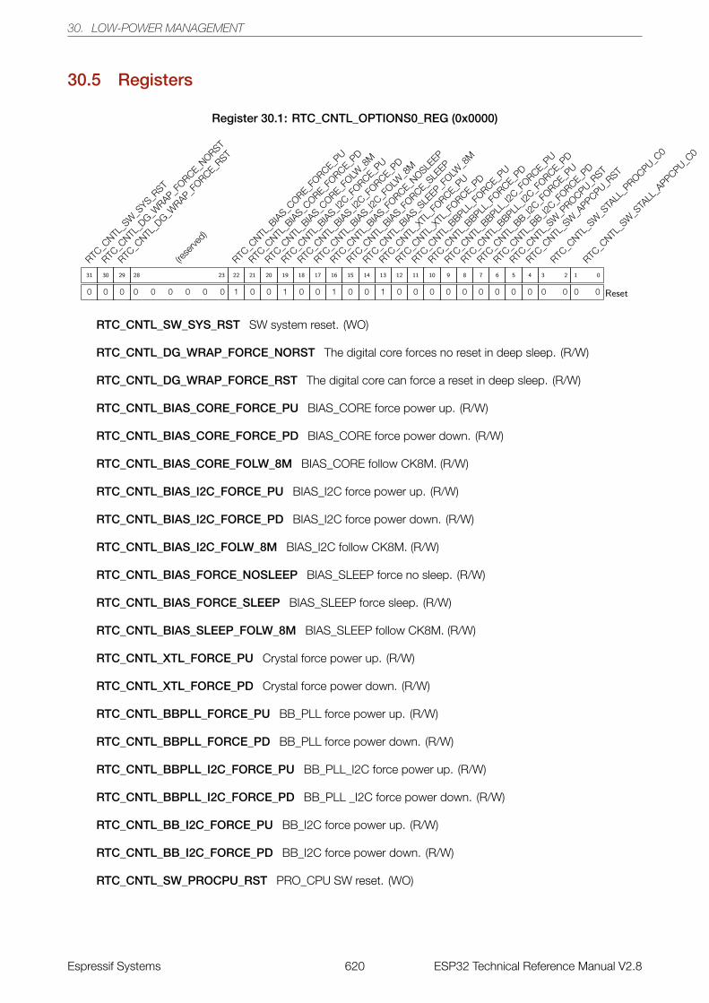
30. LOW-POWER MANAGEMENT
30.5 Registers
Register 30.1: RTC_CNTL_OPTIONS0_REG (0x0000)
RTC_C
NTL_S
W_S
YS_RST
0
31
RTC_C
NTL_D
G_WRAP_F
ORCE_NORST
0
30
RTC_C
NTL_D
G_WRAP_F
ORCE_RST
0
29
(rese
rved)
0 0 0 0 0 0
28 23
RTC_C
NTL_B
IAS_C
ORE_FORCE_P
U
1
22
RTC_C
NTL_B
IAS_C
ORE_FORCE_P
D
0
21
RTC_C
NTL_B
IAS_C
ORE_FOLW
_8M
0
20
RTC_C
NTL_B
IAS_I2
C_FORCE_P
U
1
19
RTC_C
NTL_B
IAS_I2
C_FORCE_P
D
0
18
RTC_C
NTL_B
IAS_I2
C_FOLW
_8M
0
17
RTC_C
NTL_B
IAS_F
ORCE_NOSLE
EP
1
16
RTC_C
NTL_B
IAS_F
ORCE_SLE
EP
0
15
RTC_C
NTL_B
IAS_S
LEEP_F
OLW_8
M
0
14
RTC_C
NTL_X
TL_F
ORCE_PU
1
13
RTC_C
NTL_X
TL_F
ORCE_PD
0
12
RTC_C
NTL_B
BPLL_F
ORCE_PU
0
11
RTC_C
NTL_B
BPLL_F
ORCE_PD
0
10
RTC_C
NTL_B
BPLL_I2
C_FORCE_P
U
0
9
RTC_C
NTL_B
BPLL_I2
C_FORCE_P
D
0
8
RTC_C
NTL_B
B_I2C_F
ORCE_PU
0
7
RTC_C
NTL_B
B_I2C_F
ORCE_PD
0
6
RTC_C
NTL_S
W_P
ROCPU_RST
0
5
RTC_C
NTL_S
W_A
PPCPU_RST
0
4
RTC_C
NTL_S
W_S
TALL
_PROCPU_C
0
0 0
3 2
RTC_C
NTL_S
W_S
TALL
_APPCPU_C
0
0 0
1 0
Reset
RTC_CNTL_SW_SYS_RST SW system reset. (WO)
RTC_CNTL_DG_WRAP_FORCE_NORST The digital core forces no reset in deep sleep. (R/W)
RTC_CNTL_DG_WRAP_FORCE_RST The digital core can force a reset in deep sleep. (R/W)
RTC_CNTL_BIAS_CORE_FORCE_PU BIAS_CORE force power up. (R/W)
RTC_CNTL_BIAS_CORE_FORCE_PD BIAS_CORE force power down. (R/W)
RTC_CNTL_BIAS_CORE_FOLW_8M BIAS_CORE follow CK8M. (R/W)
RTC_CNTL_BIAS_I2C_FORCE_PU BIAS_I2C force power up. (R/W)
RTC_CNTL_BIAS_I2C_FORCE_PD BIAS_I2C force power down. (R/W)
RTC_CNTL_BIAS_I2C_FOLW_8M BIAS_I2C follow CK8M. (R/W)
RTC_CNTL_BIAS_FORCE_NOSLEEP BIAS_SLEEP force no sleep. (R/W)
RTC_CNTL_BIAS_FORCE_SLEEP BIAS_SLEEP force sleep. (R/W)
RTC_CNTL_BIAS_SLEEP_FOLW_8M BIAS_SLEEP follow CK8M. (R/W)
RTC_CNTL_XTL_FORCE_PU Crystal force power up. (R/W)
RTC_CNTL_XTL_FORCE_PD Crystal force power down. (R/W)
RTC_CNTL_BBPLL_FORCE_PU BB_PLL force power up. (R/W)
RTC_CNTL_BBPLL_FORCE_PD BB_PLL force power down. (R/W)
RTC_CNTL_BBPLL_I2C_FORCE_PU BB_PLL_I2C force power up. (R/W)
RTC_CNTL_BBPLL_I2C_FORCE_PD BB_PLL _I2C force power down. (R/W)
RTC_CNTL_BB_I2C_FORCE_PU BB_I2C force power up. (R/W)
RTC_CNTL_BB_I2C_FORCE_PD BB_I2C force power down. (R/W)
RTC_CNTL_SW_PROCPU_RST PRO_CPU SW reset. (WO)
Espressif Systems 620 ESP32 Technical Reference Manual V2.8
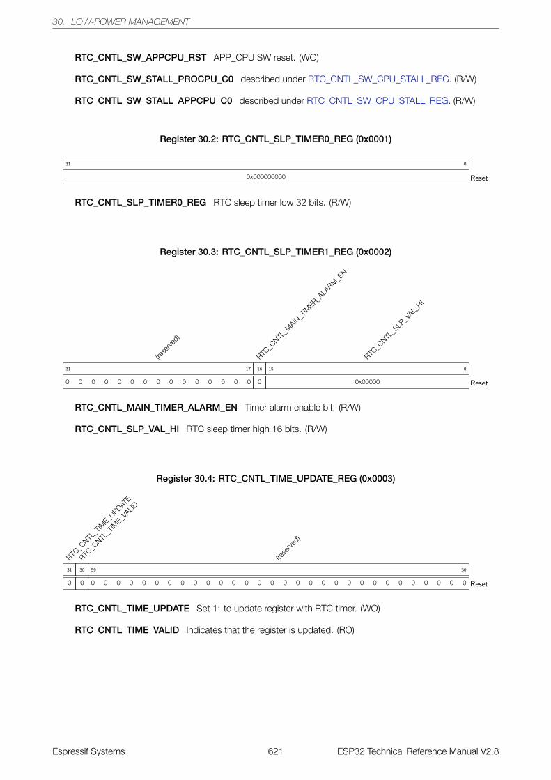
30. LOW-POWER MANAGEMENT
RTC_CNTL_SW_APPCPU_RST APP_CPU SW reset. (WO)
RTC_CNTL_SW_STALL_PROCPU_C0 described under RTC_CNTL_SW_CPU_STALL_REG. (R/W)
RTC_CNTL_SW_STALL_APPCPU_C0 described under RTC_CNTL_SW_CPU_STALL_REG. (R/W)
Register 30.2: RTC_CNTL_SLP_TIMER0_REG (0x0001)
0x000000000
31 0
Reset
RTC_CNTL_SLP_TIMER0_REG RTC sleep timer low 32 bits. (R/W)
Register 30.3: RTC_CNTL_SLP_TIMER1_REG (0x0002)
(rese
rved)
0 0 0 0 0 0 0 0 0 0 0 0 0 0 0
31 17
RTC_C
NTL_M
AIN_T
IMER_A
LARM
_EN
0
16
RTC_C
NTL_S
LP_V
AL_HI
0x00000
15 0
Reset
RTC_CNTL_MAIN_TIMER_ALARM_EN Timer alarm enable bit. (R/W)
RTC_CNTL_SLP_VAL_HI RTC sleep timer high 16 bits. (R/W)
Register 30.4: RTC_CNTL_TIME_UPDATE_REG (0x0003)
RTC_C
NTL_T
IME_U
PDATE
0
31
RTC_C
NTL_T
IME_V
ALID
0
30
(rese
rved)
0 0 0 0 0 0 0 0 0 0 0 0 0 0 0 0 0 0 0 0 0 0 0 0 0 0 0 0 0 0
59 30
Reset
RTC_CNTL_TIME_UPDATE Set 1: to update register with RTC timer. (WO)
RTC_CNTL_TIME_VALID Indicates that the register is updated. (RO)
Espressif Systems 621 ESP32 Technical Reference Manual V2.8
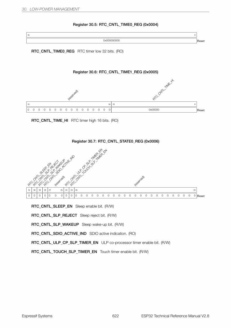
30. LOW-POWER MANAGEMENT
Register 30.5: RTC_CNTL_TIME0_REG (0x0004)
0x000000000
31 0
Reset
RTC_CNTL_TIME0_REG RTC timer low 32 bits. (RO)
Register 30.6: RTC_CNTL_TIME1_REG (0x0005)
(rese
rved)
0 0 0 0 0 0 0 0 0 0 0 0 0 0 0 0
31 16
RTC_C
NTL_T
IME_H
I
0x00000
15 0
Reset
RTC_CNTL_TIME_HI RTC timer high 16 bits. (RO)
Register 30.7: RTC_CNTL_STATE0_REG (0x0006)
RTC_C
NTL_S
LEEP_E
N
0
31
RTC_C
NTL_S
LP_R
EJECT
0
30
RTC_C
NTL_S
LP_W
AKEUP
0
29
RTC_C
NTL_S
DIO_A
CTIVE_IN
D
0
28
(rese
rved)
0 0 0
27 25
RTC_C
NTL_U
LP_C
P_SLP
_TIM
ER_EN
0
24
RTC_C
NTL_T
OUCH_SLP
_TIM
ER_EN
0
23
(rese
rved)
0 0 0 0 0 0 0 0 0 0 0 0 0 0 0 0 0 0 0 0 0 0 0
45 23
Reset
RTC_CNTL_SLEEP_EN Sleep enable bit. (R/W)
RTC_CNTL_SLP_REJECT Sleep reject bit. (R/W)
RTC_CNTL_SLP_WAKEUP Sleep wake-up bit. (R/W)
RTC_CNTL_SDIO_ACTIVE_IND SDIO active indication. (RO)
RTC_CNTL_ULP_CP_SLP_TIMER_EN ULP co-processor timer enable bit. (R/W)
RTC_CNTL_TOUCH_SLP_TIMER_EN Touch timer enable bit. (R/W)
Espressif Systems 622 ESP32 Technical Reference Manual V2.8
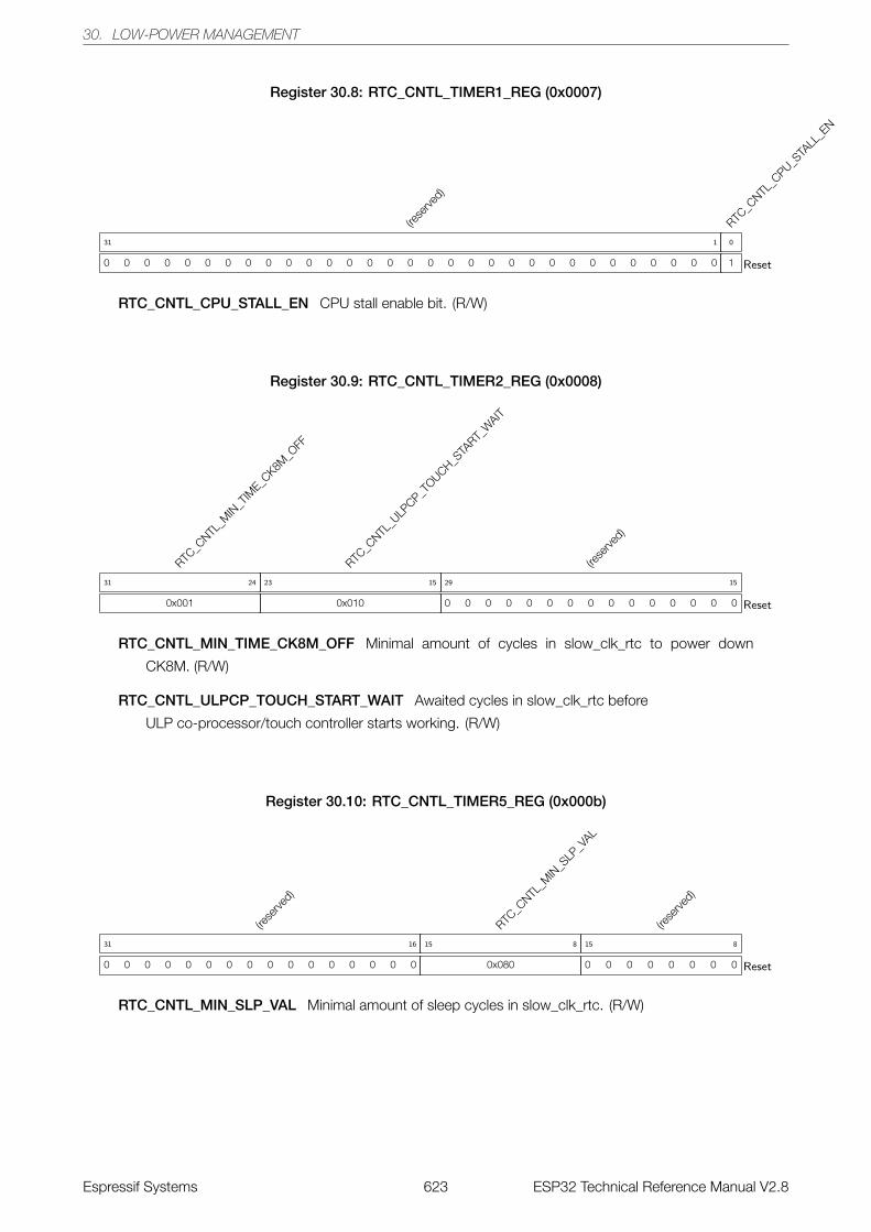
30. LOW-POWER MANAGEMENT
Register 30.8: RTC_CNTL_TIMER1_REG (0x0007)
(rese
rved)
0 0 0 0 0 0 0 0 0 0 0 0 0 0 0 0 0 0 0 0 0 0 0 0 0 0 0 0 0 0 0
31 1
RTC_C
NTL_C
PU_STA
LL_E
N
1
0
Reset
RTC_CNTL_CPU_STALL_EN CPU stall enable bit. (R/W)
Register 30.9: RTC_CNTL_TIMER2_REG (0x0008)
RTC_C
NTL_M
IN_T
IME_C
K8M_O
FF
0x001
31 24
RTC_C
NTL_U
LPCP_T
OUCH_STA
RT_W
AIT
0x010
23 15
(rese
rved)
0 0 0 0 0 0 0 0 0 0 0 0 0 0 0
29 15
Reset
RTC_CNTL_MIN_TIME_CK8M_OFF Minimal amount of cycles in slow_clk_rtc to power down
CK8M. (R/W)
RTC_CNTL_ULPCP_TOUCH_START_WAIT Awaited cycles in slow_clk_rtc before
ULP co-processor/touch controller starts working. (R/W)
Register 30.10: RTC_CNTL_TIMER5_REG (0x000b)
(rese
rved)
0 0 0 0 0 0 0 0 0 0 0 0 0 0 0 0
31 16
RTC_C
NTL_M
IN_S
LP_V
AL
0x080
15 8
(rese
rved)
0 0 0 0 0 0 0 0
15 8
Reset
RTC_CNTL_MIN_SLP_VAL Minimal amount of sleep cycles in slow_clk_rtc. (R/W)
Espressif Systems 623 ESP32 Technical Reference Manual V2.8
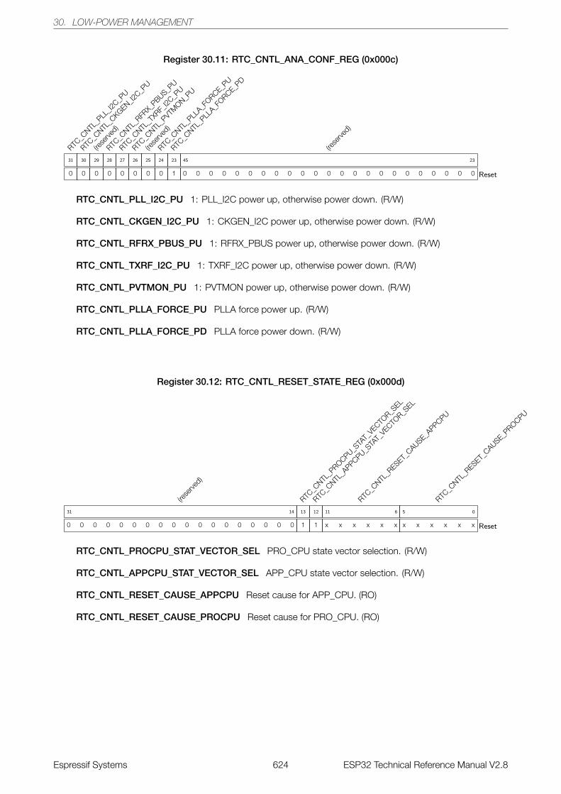
30. LOW-POWER MANAGEMENT
Register 30.11: RTC_CNTL_ANA_CONF_REG (0x000c)
RTC_C
NTL_P
LL_I2
C_PU
0
31
RTC_C
NTL_C
KGEN_I2C_P
U
0
30
(rese
rved)
0
29
RTC_C
NTL_R
FRX_
PBUS_PU
0
28
RTC_C
NTL_T
XRF_
I2C_P
U
0
27
RTC_C
NTL_P
VTMON_P
U
0
26
(rese
rved)
0
25
RTC_C
NTL_P
LLA_F
ORCE_PU
0
24
RTC_C
NTL_P
LLA_F
ORCE_PD
1
23
(rese
rved)
0 0 0 0 0 0 0 0 0 0 0 0 0 0 0 0 0 0 0 0 0 0 0
45 23
Reset
RTC_CNTL_PLL_I2C_PU 1: PLL_I2C power up, otherwise power down. (R/W)
RTC_CNTL_CKGEN_I2C_PU 1: CKGEN_I2C power up, otherwise power down. (R/W)
RTC_CNTL_RFRX_PBUS_PU 1: RFRX_PBUS power up, otherwise power down. (R/W)
RTC_CNTL_TXRF_I2C_PU 1: TXRF_I2C power up, otherwise power down. (R/W)
RTC_CNTL_PVTMON_PU 1: PVTMON power up, otherwise power down. (R/W)
RTC_CNTL_PLLA_FORCE_PU PLLA force power up. (R/W)
RTC_CNTL_PLLA_FORCE_PD PLLA force power down. (R/W)
Register 30.12: RTC_CNTL_RESET_STATE_REG (0x000d)
(rese
rved)
0 0 0 0 0 0 0 0 0 0 0 0 0 0 0 0 0 0
31 14
RTC_C
NTL_P
ROCPU_STA
T_VECTO
R_SEL
1
13
RTC_C
NTL_A
PPCPU_STA
T_VECTO
R_SEL
1
12
RTC_C
NTL_R
ESET_CAUSE_A
PPCPU
x x x x x x
11 6
RTC_C
NTL_R
ESET_CAUSE_P
ROCPU
x x x x x x
5 0
Reset
RTC_CNTL_PROCPU_STAT_VECTOR_SEL PRO_CPU state vector selection. (R/W)
RTC_CNTL_APPCPU_STAT_VECTOR_SEL APP_CPU state vector selection. (R/W)
RTC_CNTL_RESET_CAUSE_APPCPU Reset cause for APP_CPU. (RO)
RTC_CNTL_RESET_CAUSE_PROCPU Reset cause for PRO_CPU. (RO)
Espressif Systems 624 ESP32 Technical Reference Manual V2.8
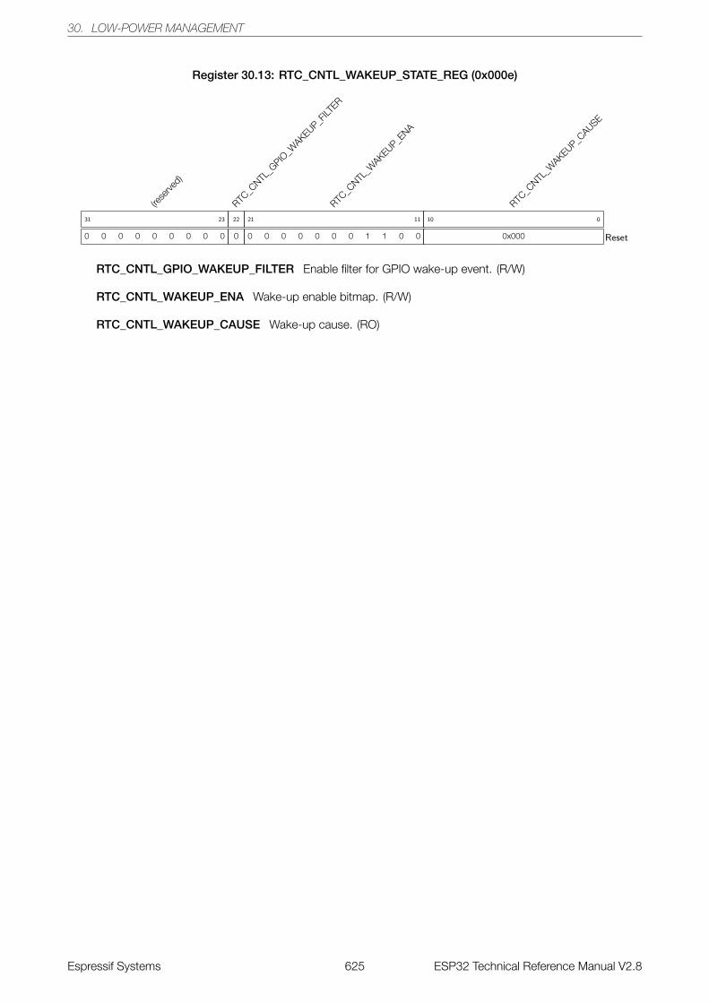
30. LOW-POWER MANAGEMENT
Register 30.13: RTC_CNTL_WAKEUP_STATE_REG (0x000e)
(rese
rved)
0 0 0 0 0 0 0 0 0
31 23
RTC_C
NTL_G
PIO_W
AKEUP_FILT
ER
0
22
RTC_C
NTL_W
AKEUP_ENA
0 0 0 0 0 0 0 1 1 0 0
21 11
RTC_C
NTL_W
AKEUP_CAUSE
0x000
10 0
Reset
RTC_CNTL_GPIO_WAKEUP_FILTER Enable filter for GPIO wake-up event. (R/W)
RTC_CNTL_WAKEUP_ENA Wake-up enable bitmap. (R/W)
RTC_CNTL_WAKEUP_CAUSE Wake-up cause. (RO)
Espressif Systems 625 ESP32 Technical Reference Manual V2.8
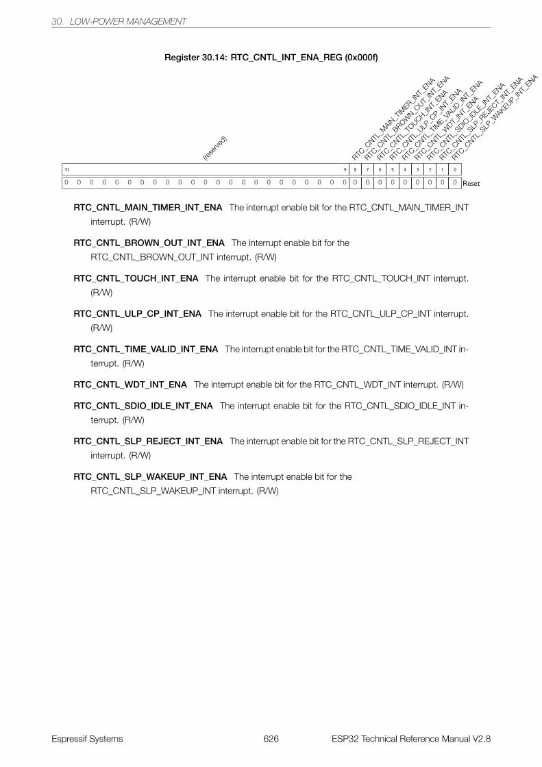
30. LOW-POWER MANAGEMENT
Register 30.14: RTC_CNTL_INT_ENA_REG (0x000f)
(rese
rved)
0 0 0 0 0 0 0 0 0 0 0 0 0 0 0 0 0 0 0 0 0 0 0
31 9
RTC_C
NTL_M
AIN_T
IMER_IN
T_ENA
0
8
RTC_C
NTL_B
ROWN_O
UT_IN
T_ENA
0
7
RTC_C
NTL_T
OUCH_INT_
ENA
0
6
RTC_C
NTL_U
LP_C
P_INT_
ENA
0
5
RTC_C
NTL_T
IME_V
ALID_IN
T_ENA
0
4
RTC_C
NTL_W
DT_IN
T_ENA
0
3
RTC_C
NTL_S
DIO_ID
LE_IN
T_ENA
0
2
RTC_C
NTL_S
LP_R
EJECT_
INT_
ENA
0
1
RTC_C
NTL_S
LP_W
AKEUP_INT_
ENA
0
0
Reset
RTC_CNTL_MAIN_TIMER_INT_ENA The interrupt enable bit for the RTC_CNTL_MAIN_TIMER_INT
interrupt. (R/W)
RTC_CNTL_BROWN_OUT_INT_ENA The interrupt enable bit for the
RTC_CNTL_BROWN_OUT_INT interrupt. (R/W)
RTC_CNTL_TOUCH_INT_ENA The interrupt enable bit for the RTC_CNTL_TOUCH_INT interrupt.
(R/W)
RTC_CNTL_ULP_CP_INT_ENA The interrupt enable bit for the RTC_CNTL_ULP_CP_INT interrupt.
(R/W)
RTC_CNTL_TIME_VALID_INT_ENA The interrupt enable bit for the RTC_CNTL_TIME_VALID_INT in-
terrupt. (R/W)
RTC_CNTL_WDT_INT_ENA The interrupt enable bit for the RTC_CNTL_WDT_INT interrupt. (R/W)
RTC_CNTL_SDIO_IDLE_INT_ENA The interrupt enable bit for the RTC_CNTL_SDIO_IDLE_INT in-
terrupt. (R/W)
RTC_CNTL_SLP_REJECT_INT_ENA The interrupt enable bit for the RTC_CNTL_SLP_REJECT_INT
interrupt. (R/W)
RTC_CNTL_SLP_WAKEUP_INT_ENA The interrupt enable bit for the
RTC_CNTL_SLP_WAKEUP_INT interrupt. (R/W)
Espressif Systems 626 ESP32 Technical Reference Manual V2.8
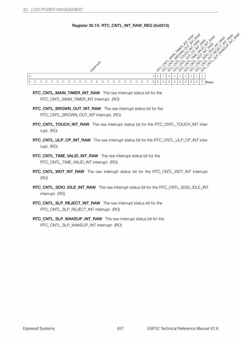
30. LOW-POWER MANAGEMENT
Register 30.15: RTC_CNTL_INT_RAW_REG (0x0010)
(rese
rved)
0 0 0 0 0 0 0 0 0 0 0 0 0 0 0 0 0 0 0 0 0 0 0
31 9
RTC_C
NTL_M
AIN_T
IMER_IN
T_RAW
0
8
RTC_C
NTL_B
ROWN_O
UT_IN
T_RAW
0
7
RTC_C
NTL_T
OUCH_INT_
RAW
0
6
RTC_C
NTL_U
LP_C
P_INT_
RAW
0
5
RTC_C
NTL_T
IME_V
ALID_IN
T_RAW
0
4
RTC_C
NTL_W
DT_IN
T_RAW
0
3
RTC_C
NTL_S
DIO_ID
LE_IN
T_RAW
0
2
RTC_C
NTL_S
LP_R
EJECT_
INT_
RAW
0
1
RTC_C
NTL_S
LP_W
AKEUP_INT_
RAW
0
0
Reset
RTC_CNTL_MAIN_TIMER_INT_RAW The raw interrupt status bit for the
RTC_CNTL_MAIN_TIMER_INT interrupt. (RO)
RTC_CNTL_BROWN_OUT_INT_RAW The raw interrupt status bit for the
RTC_CNTL_BROWN_OUT_INT interrupt. (RO)
RTC_CNTL_TOUCH_INT_RAW The raw interrupt status bit for the RTC_CNTL_TOUCH_INT inter-
rupt. (RO)
RTC_CNTL_ULP_CP_INT_RAW The raw interrupt status bit for the RTC_CNTL_ULP_CP_INT inter-
rupt. (RO)
RTC_CNTL_TIME_VALID_INT_RAW The raw interrupt status bit for the
RTC_CNTL_TIME_VALID_INT interrupt. (RO)
RTC_CNTL_WDT_INT_RAW The raw interrupt status bit for the RTC_CNTL_WDT_INT interrupt.
(RO)
RTC_CNTL_SDIO_IDLE_INT_RAW The raw interrupt status bit for the RTC_CNTL_SDIO_IDLE_INT
interrupt. (RO)
RTC_CNTL_SLP_REJECT_INT_RAW The raw interrupt status bit for the
RTC_CNTL_SLP_REJECT_INT interrupt. (RO)
RTC_CNTL_SLP_WAKEUP_INT_RAW The raw interrupt status bit for the
RTC_CNTL_SLP_WAKEUP_INT interrupt. (RO)
Espressif Systems 627 ESP32 Technical Reference Manual V2.8
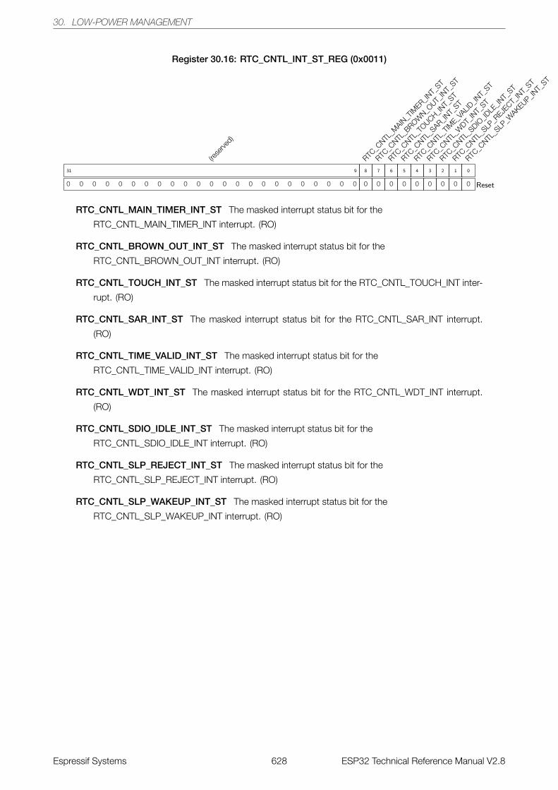
30. LOW-POWER MANAGEMENT
Register 30.16: RTC_CNTL_INT_ST_REG (0x0011)
(rese
rved)
0 0 0 0 0 0 0 0 0 0 0 0 0 0 0 0 0 0 0 0 0 0 0
31 9
RTC_C
NTL_M
AIN_T
IMER_IN
T_ST
0
8
RTC_C
NTL_B
ROWN_O
UT_IN
T_ST
0
7
RTC_C
NTL_T
OUCH_INT_
ST
0
6
RTC_C
NTL_S
AR_INT_
ST
0
5
RTC_C
NTL_T
IME_V
ALID_IN
T_ST
0
4
RTC_C
NTL_W
DT_IN
T_ST
0
3
RTC_C
NTL_S
DIO_ID
LE_IN
T_ST
0
2
RTC_C
NTL_S
LP_R
EJECT_
INT_
ST
0
1
RTC_C
NTL_S
LP_W
AKEUP_INT_
ST
0
0
Reset
RTC_CNTL_MAIN_TIMER_INT_ST The masked interrupt status bit for the
RTC_CNTL_MAIN_TIMER_INT interrupt. (RO)
RTC_CNTL_BROWN_OUT_INT_ST The masked interrupt status bit for the
RTC_CNTL_BROWN_OUT_INT interrupt. (RO)
RTC_CNTL_TOUCH_INT_ST The masked interrupt status bit for the RTC_CNTL_TOUCH_INT inter-
rupt. (RO)
RTC_CNTL_SAR_INT_ST The masked interrupt status bit for the RTC_CNTL_SAR_INT interrupt.
(RO)
RTC_CNTL_TIME_VALID_INT_ST The masked interrupt status bit for the
RTC_CNTL_TIME_VALID_INT interrupt. (RO)
RTC_CNTL_WDT_INT_ST The masked interrupt status bit for the RTC_CNTL_WDT_INT interrupt.
(RO)
RTC_CNTL_SDIO_IDLE_INT_ST The masked interrupt status bit for the
RTC_CNTL_SDIO_IDLE_INT interrupt. (RO)
RTC_CNTL_SLP_REJECT_INT_ST The masked interrupt status bit for the
RTC_CNTL_SLP_REJECT_INT interrupt. (RO)
RTC_CNTL_SLP_WAKEUP_INT_ST The masked interrupt status bit for the
RTC_CNTL_SLP_WAKEUP_INT interrupt. (RO)
Espressif Systems 628 ESP32 Technical Reference Manual V2.8
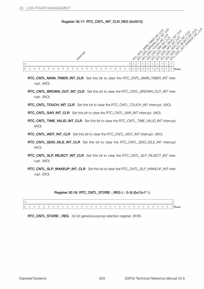
30. LOW-POWER MANAGEMENT
Register 30.17: RTC_CNTL_INT_CLR_REG (0x0012)
(rese
rved)
0 0 0 0 0 0 0 0 0 0 0 0 0 0 0 0 0 0 0 0 0 0 0
31 9
RTC_C
NTL_M
AIN_T
IMER_IN
T_CLR
0
8
RTC_C
NTL_B
ROWN_O
UT_IN
T_CLR
0
7
RTC_C
NTL_T
OUCH_INT_
CLR
0
6
RTC_C
NTL_S
AR_INT_
CLR
0
5
RTC_C
NTL_T
IME_V
ALID_IN
T_CLR
0
4
RTC_C
NTL_W
DT_IN
T_CLR
0
3
RTC_C
NTL_S
DIO_ID
LE_IN
T_CLR
0
2
RTC_C
NTL_S
LP_R
EJECT_
INT_
CLR
0
1
RTC_C
NTL_S
LP_W
AKEUP_INT_
CLR
0
0
Reset
RTC_CNTL_MAIN_TIMER_INT_CLR Set this bit to clear the RTC_CNTL_MAIN_TIMER_INT inter-
rupt. (WO)
RTC_CNTL_BROWN_OUT_INT_CLR Set this bit to clear the RTC_CNTL_BROWN_OUT_INT inter-
rupt. (WO)
RTC_CNTL_TOUCH_INT_CLR Set this bit to clear the RTC_CNTL_TOUCH_INT interrupt. (WO)
RTC_CNTL_SAR_INT_CLR Set this bit to clear the RTC_CNTL_SAR_INT interrupt. (WO)
RTC_CNTL_TIME_VALID_INT_CLR Set this bit to clear the RTC_CNTL_TIME_VALID_INT interrupt.
(WO)
RTC_CNTL_WDT_INT_CLR Set this bit to clear the RTC_CNTL_WDT_INT interrupt. (WO)
RTC_CNTL_SDIO_IDLE_INT_CLR Set this bit to clear the RTC_CNTL_SDIO_IDLE_INT interrupt.
(WO)
RTC_CNTL_SLP_REJECT_INT_CLR Set this bit to clear the RTC_CNTL_SLP_REJECT_INT inter-
rupt. (WO)
RTC_CNTL_SLP_WAKEUP_INT_CLR Set this bit to clear the RTC_CNTL_SLP_WAKEUP_INT inter-
rupt. (WO)
Register 30.18: RTC_CNTL_STOREn_REG (n: 0-3) (0x13+1*n)
x x x x x x x x x x x x x x x x x x x x x x x x x x x x x x x x
31 0
Reset
RTC_CNTL_STOREn_REG 32-bit general-purpose retention register. (R/W)
Espressif Systems 629 ESP32 Technical Reference Manual V2.8
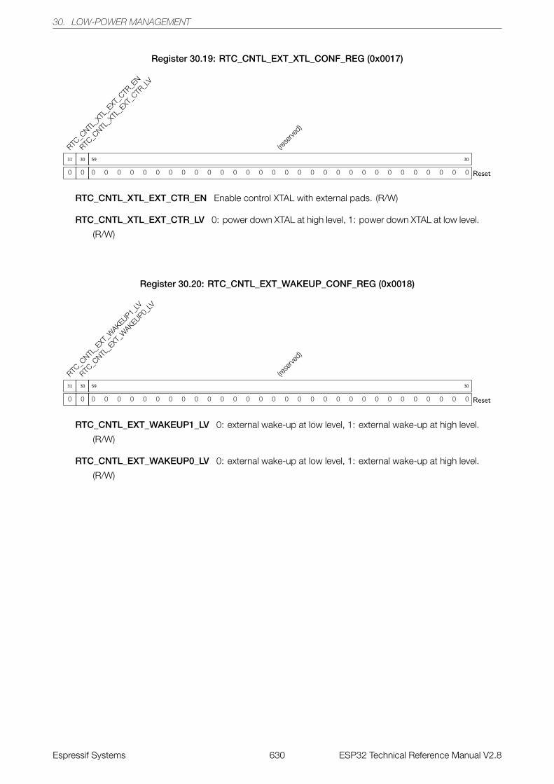
30. LOW-POWER MANAGEMENT
Register 30.19: RTC_CNTL_EXT_XTL_CONF_REG (0x0017)
RTC_C
NTL_X
TL_E
XT_C
TR_E
N
0
31
RTC_C
NTL_X
TL_E
XT_C
TR_L
V
0
30
(rese
rved)
0 0 0 0 0 0 0 0 0 0 0 0 0 0 0 0 0 0 0 0 0 0 0 0 0 0 0 0 0 0
59 30
Reset
RTC_CNTL_XTL_EXT_CTR_EN Enable control XTAL with external pads. (R/W)
RTC_CNTL_XTL_EXT_CTR_LV 0: power down XTAL at high level, 1: power down XTAL at low level.
(R/W)
Register 30.20: RTC_CNTL_EXT_WAKEUP_CONF_REG (0x0018)
RTC_C
NTL_E
XT_W
AKEUP1_LV
0
31
RTC_C
NTL_E
XT_W
AKEUP0_LV
0
30
(rese
rved)
0 0 0 0 0 0 0 0 0 0 0 0 0 0 0 0 0 0 0 0 0 0 0 0 0 0 0 0 0 0
59 30
Reset
RTC_CNTL_EXT_WAKEUP1_LV 0: external wake-up at low level, 1: external wake-up at high level.
(R/W)
RTC_CNTL_EXT_WAKEUP0_LV 0: external wake-up at low level, 1: external wake-up at high level.
(R/W)
Espressif Systems 630 ESP32 Technical Reference Manual V2.8
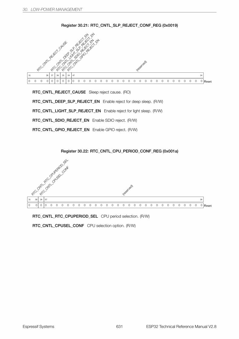
30. LOW-POWER MANAGEMENT
Register 30.21: RTC_CNTL_SLP_REJECT_CONF_REG (0x0019)
RTC_C
NTL_R
EJECT_
CAUSE
0 0 0 0
31 28
RTC_C
NTL_D
EEP_SLP
_REJE
CT_EN
0
27
RTC_C
NTL_L
IGHT_
SLP_R
EJECT_
EN
0
26
RTC_C
NTL_S
DIO_R
EJECT_
EN
0
25
RTC_C
NTL_G
PIO_R
EJECT_
EN
0
24
(rese
rved)
0 0 0 0 0 0 0 0 0 0 0 0 0 0 0 0 0 0 0 0 0 0 0 0
47 24
Reset
RTC_CNTL_REJECT_CAUSE Sleep reject cause. (RO)
RTC_CNTL_DEEP_SLP_REJECT_EN Enable reject for deep sleep. (R/W)
RTC_CNTL_LIGHT_SLP_REJECT_EN Enable reject for light sleep. (R/W)
RTC_CNTL_SDIO_REJECT_EN Enable SDIO reject. (R/W)
RTC_CNTL_GPIO_REJECT_EN Enable GPIO reject. (R/W)
Register 30.22: RTC_CNTL_CPU_PERIOD_CONF_REG (0x001a)
RTC_C
NTL_R
TC_C
PUPERIOD_S
EL
0 0
31 30
RTC_C
NTL_C
PUSEL_CONF
0
29
(rese
rved)
0 0 0 0 0 0 0 0 0 0 0 0 0 0 0 0 0 0 0 0 0 0 0 0 0 0 0 0 0
57 29
Reset
RTC_CNTL_RTC_CPUPERIOD_SEL CPU period selection. (R/W)
RTC_CNTL_CPUSEL_CONF CPU selection option. (R/W)
Espressif Systems 631 ESP32 Technical Reference Manual V2.8
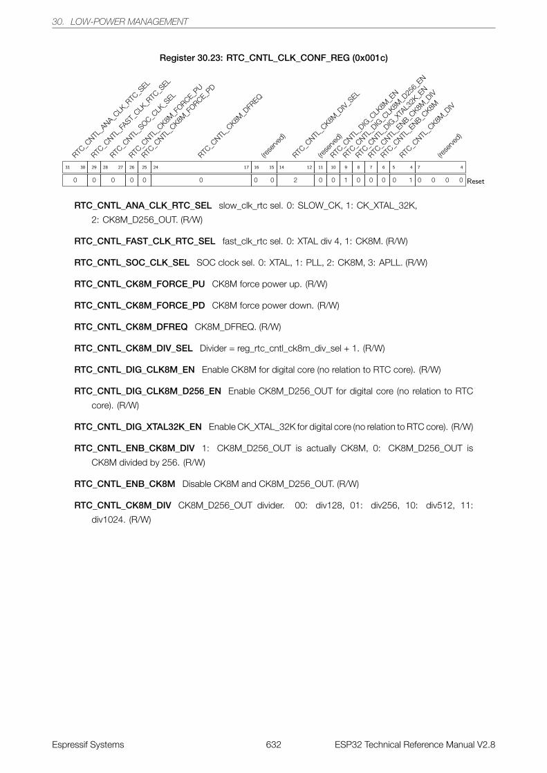
30. LOW-POWER MANAGEMENT
Register 30.23: RTC_CNTL_CLK_CONF_REG (0x001c)
RTC_C
NTL_A
NA_CLK
_RTC
_SEL
0
31 30
RTC_C
NTL_F
AST_CLK
_RTC
_SEL
0
29
RTC_C
NTL_S
OC_CLK
_SEL
0
28 27
RTC_C
NTL_C
K8M_F
ORCE_PU
0
26
RTC_C
NTL_C
K8M_F
ORCE_PD
0
25
RTC_C
NTL_C
K8M_D
FREQ
0
24 17
(rese
rved)
0 0
16 15
RTC_C
NTL_C
K8M_D
IV_SEL
2
14 12
(rese
rved)
0
11
RTC_C
NTL_D
IG_C
LK8M
_EN
0
10
RTC_C
NTL_D
IG_C
LK8M
_D25
6_EN
1
9
RTC_C
NTL_D
IG_X
TAL3
2K_E
N
0
8
RTC_C
NTL_E
NB_CK8M
_DIV
0
7
RTC_C
NTL_E
NB_CK8M
0
6
RTC_C
NTL_C
K8M_D
IV
0 1
5 4
(rese
rved)
0 0 0 0
7 4
Reset
RTC_CNTL_ANA_CLK_RTC_SEL slow_clk_rtc sel. 0: SLOW_CK, 1: CK_XTAL_32K,
2: CK8M_D256_OUT. (R/W)
RTC_CNTL_FAST_CLK_RTC_SEL fast_clk_rtc sel. 0: XTAL div 4, 1: CK8M. (R/W)
RTC_CNTL_SOC_CLK_SEL SOC clock sel. 0: XTAL, 1: PLL, 2: CK8M, 3: APLL. (R/W)
RTC_CNTL_CK8M_FORCE_PU CK8M force power up. (R/W)
RTC_CNTL_CK8M_FORCE_PD CK8M force power down. (R/W)
RTC_CNTL_CK8M_DFREQ CK8M_DFREQ. (R/W)
RTC_CNTL_CK8M_DIV_SEL Divider = reg_rtc_cntl_ck8m_div_sel + 1. (R/W)
RTC_CNTL_DIG_CLK8M_EN Enable CK8M for digital core (no relation to RTC core). (R/W)
RTC_CNTL_DIG_CLK8M_D256_EN Enable CK8M_D256_OUT for digital core (no relation to RTC
core). (R/W)
RTC_CNTL_DIG_XTAL32K_EN Enable CK_XTAL_32K for digital core (no relation to RTC core). (R/W)
RTC_CNTL_ENB_CK8M_DIV 1: CK8M_D256_OUT is actually CK8M, 0: CK8M_D256_OUT is
CK8M divided by 256. (R/W)
RTC_CNTL_ENB_CK8M Disable CK8M and CK8M_D256_OUT. (R/W)
RTC_CNTL_CK8M_DIV CK8M_D256_OUT divider. 00: div128, 01: div256, 10: div512, 11:
div1024. (R/W)
Espressif Systems 632 ESP32 Technical Reference Manual V2.8
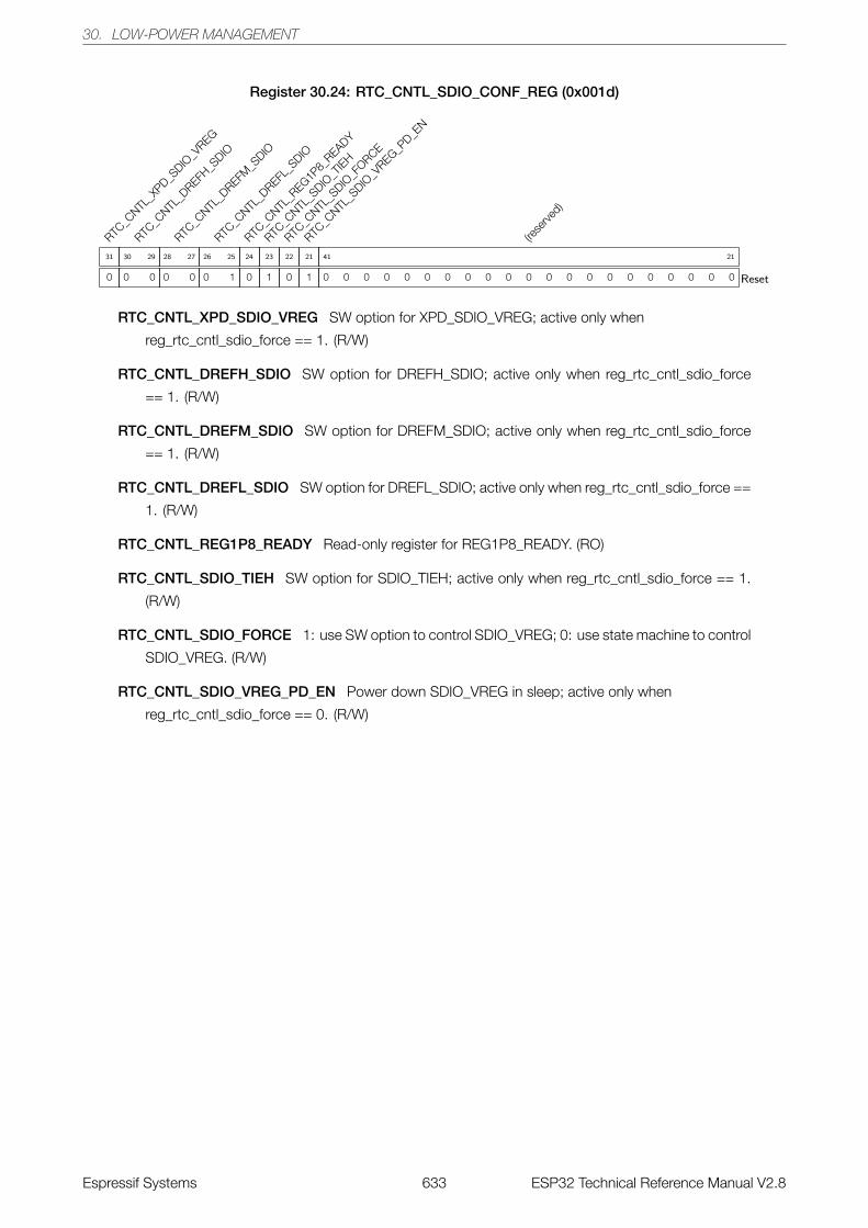
30. LOW-POWER MANAGEMENT
Register 30.24: RTC_CNTL_SDIO_CONF_REG (0x001d)
RTC_C
NTL_X
PD_SDIO
_VREG
0
31
RTC_C
NTL_D
REFH_S
DIO
0 0
30 29
RTC_C
NTL_D
REFM_S
DIO
0 0
28 27
RTC_C
NTL_D
REFL_S
DIO
0 1
26 25
RTC_C
NTL_R
EG1P8_
READY
0
24
RTC_C
NTL_S
DIO_T
IEH
1
23
RTC_C
NTL_S
DIO_F
ORCE
0
22
RTC_C
NTL_S
DIO_V
REG_PD_E
N
1
21
(rese
rved)
0 0 0 0 0 0 0 0 0 0 0 0 0 0 0 0 0 0 0 0 0
41 21
Reset
RTC_CNTL_XPD_SDIO_VREG SW option for XPD_SDIO_VREG; active only when
reg_rtc_cntl_sdio_force == 1. (R/W)
RTC_CNTL_DREFH_SDIO SW option for DREFH_SDIO; active only when reg_rtc_cntl_sdio_force
== 1. (R/W)
RTC_CNTL_DREFM_SDIO SW option for DREFM_SDIO; active only when reg_rtc_cntl_sdio_force
== 1. (R/W)
RTC_CNTL_DREFL_SDIO SW option for DREFL_SDIO; active only when reg_rtc_cntl_sdio_force ==
1. (R/W)
RTC_CNTL_REG1P8_READY Read-only register for REG1P8_READY. (RO)
RTC_CNTL_SDIO_TIEH SW option for SDIO_TIEH; active only when reg_rtc_cntl_sdio_force == 1.
(R/W)
RTC_CNTL_SDIO_FORCE 1: use SW option to control SDIO_VREG; 0: use state machine to control
SDIO_VREG. (R/W)
RTC_CNTL_SDIO_VREG_PD_EN Power down SDIO_VREG in sleep; active only when
reg_rtc_cntl_sdio_force == 0. (R/W)
Espressif Systems 633 ESP32 Technical Reference Manual V2.8
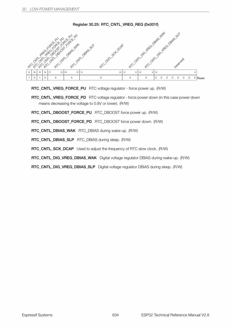
30. LOW-POWER MANAGEMENT
Register 30.25: RTC_CNTL_VREG_REG (0x001f)
RTC_C
NTL_P
REG_FORCE_P
U
1
31
RTC_C
NTL_P
REG_FORCE_P
D
0
30
RTC_C
NTL_D
BOOST_FO
RCE_PU
1
29
RTC_C
NTL_D
BOOST_FO
RCE_PD
0
28
RTC_C
NTL_D
BIAS_W
AK
4
27 25
RTC_C
NTL_D
BIAS_S
LP
4
24 22
RTC_C
NTL_S
CK_DCAP
0
21 14
RTC_C
NTL_D
IG_V
REG_DBIA
S_WAK
4
13 11
RTC_C
NTL_D
IG_V
REG_DBIA
S_SLP
4
10 8
(rese
rved)
0 0 0 0 0 0 0 0
15 8
Reset
RTC_CNTL_VREG_FORCE_PU RTC voltage regulator - force power up. (R/W)
RTC_CNTL_VREG_FORCE_PD RTC voltage regulator - force power down (in this case power down
means decreasing the voltage to 0.8V or lower). (R/W)
RTC_CNTL_DBOOST_FORCE_PU RTC_DBOOST force power up. (R/W)
RTC_CNTL_DBOOST_FORCE_PD RTC_DBOOST force power down. (R/W)
RTC_CNTL_DBIAS_WAK RTC_DBIAS during wake-up. (R/W)
RTC_CNTL_DBIAS_SLP RTC_DBIAS during sleep. (R/W)
RTC_CNTL_SCK_DCAP Used to adjust the frequency of RTC slow clock. (R/W)
RTC_CNTL_DIG_VREG_DBIAS_WAK Digital voltage regulator DBIAS during wake-up. (R/W)
RTC_CNTL_DIG_VREG_DBIAS_SLP Digital voltage regulator DBIAS during sleep. (R/W)
Espressif Systems 634 ESP32 Technical Reference Manual V2.8
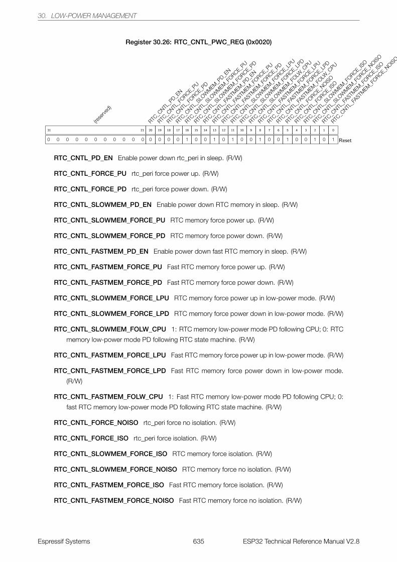
30. LOW-POWER MANAGEMENT
Register 30.26: RTC_CNTL_PWC_REG (0x0020)
(rese
rved)
0 0 0 0 0 0 0 0 0 0 0
31 21
RTC_C
NTL_P
D_EN
0
20
RTC_C
NTL_F
ORCE_PU
0
19
RTC_C
NTL_F
ORCE_PD
0
18
RTC_C
NTL_S
LOW
MEM
_PD_E
N
0
17
RTC_C
NTL_S
LOW
MEM
_FORCE_P
U
1
16
RTC_C
NTL_S
LOW
MEM
_FORCE_P
D
0
15
RTC_C
NTL_F
ASTMEM
_PD_E
N
0
14
RTC_C
NTL_F
ASTMEM
_FORCE_P
U
1
13
RTC_C
NTL_F
ASTMEM
_FORCE_P
D
0
12
RTC_C
NTL_S
LOW
MEM
_FORCE_L
PU
1
11
RTC_C
NTL_S
LOW
MEM
_FORCE_L
PD
0
10
RTC_C
NTL_S
LOW
MEM
_FOLW
_CPU
0
9
RTC_C
NTL_F
ASTMEM
_FORCE_L
PU
1
8
RTC_C
NTL_F
ASTMEM
_FORCE_L
PD
0
7
RTC_C
NTL_F
ASTMEM
_FOLW
_CPU
0
6
RTC_C
NTL_F
ORCE_NOIS
O
1
5
RTC_C
NTL_F
ORCE_ISO
0
4
RTC_C
NTL_S
LOW
MEM
_FORCE_IS
O
0
3
RTC_C
NTL_S
LOW
MEM
_FORCE_N
OISO
1
2
RTC_C
NTL_F
ASTMEM
_FORCE_IS
O
0
1
RTC_C
NTL_F
ASTMEM
_FORCE_N
OISO
1
0
Reset
RTC_CNTL_PD_EN Enable power down rtc_peri in sleep. (R/W)
RTC_CNTL_FORCE_PU rtc_peri force power up. (R/W)
RTC_CNTL_FORCE_PD rtc_peri force power down. (R/W)
RTC_CNTL_SLOWMEM_PD_EN Enable power down RTC memory in sleep. (R/W)
RTC_CNTL_SLOWMEM_FORCE_PU RTC memory force power up. (R/W)
RTC_CNTL_SLOWMEM_FORCE_PD RTC memory force power down. (R/W)
RTC_CNTL_FASTMEM_PD_EN Enable power down fast RTC memory in sleep. (R/W)
RTC_CNTL_FASTMEM_FORCE_PU Fast RTC memory force power up. (R/W)
RTC_CNTL_FASTMEM_FORCE_PD Fast RTC memory force power down. (R/W)
RTC_CNTL_SLOWMEM_FORCE_LPU RTC memory force power up in low-power mode. (R/W)
RTC_CNTL_SLOWMEM_FORCE_LPD RTC memory force power down in low-power mode. (R/W)
RTC_CNTL_SLOWMEM_FOLW_CPU 1: RTC memory low-power mode PD following CPU; 0: RTC
memory low-power mode PD following RTC state machine. (R/W)
RTC_CNTL_FASTMEM_FORCE_LPU Fast RTC memory force power up in low-power mode. (R/W)
RTC_CNTL_FASTMEM_FORCE_LPD Fast RTC memory force power down in low-power mode.
(R/W)
RTC_CNTL_FASTMEM_FOLW_CPU 1: Fast RTC memory low-power mode PD following CPU; 0:
fast RTC memory low-power mode PD following RTC state machine. (R/W)
RTC_CNTL_FORCE_NOISO rtc_peri force no isolation. (R/W)
RTC_CNTL_FORCE_ISO rtc_peri force isolation. (R/W)
RTC_CNTL_SLOWMEM_FORCE_ISO RTC memory force isolation. (R/W)
RTC_CNTL_SLOWMEM_FORCE_NOISO RTC memory force no isolation. (R/W)
RTC_CNTL_FASTMEM_FORCE_ISO Fast RTC memory force isolation. (R/W)
RTC_CNTL_FASTMEM_FORCE_NOISO Fast RTC memory force no isolation. (R/W)
Espressif Systems 635 ESP32 Technical Reference Manual V2.8
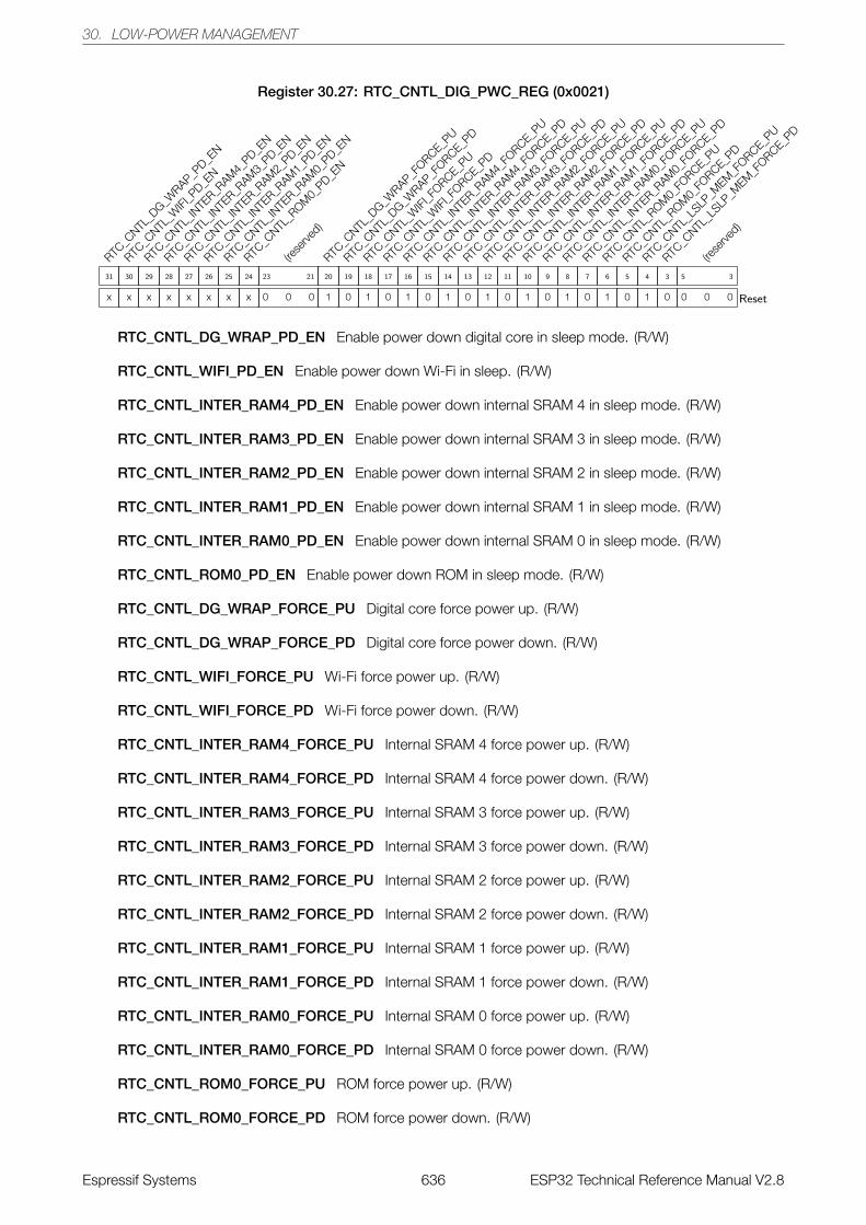
30. LOW-POWER MANAGEMENT
Register 30.27: RTC_CNTL_DIG_PWC_REG (0x0021)
RTC_C
NTL_D
G_WRAP_P
D_EN
x
31
RTC_C
NTL_W
IFI_P
D_EN
x
30
RTC_C
NTL_IN
TER_R
AM4_
PD_EN
x
29
RTC_C
NTL_IN
TER_R
AM3_
PD_EN
x
28
RTC_C
NTL_IN
TER_R
AM2_
PD_EN
x
27
RTC_C
NTL_IN
TER_R
AM1_
PD_EN
x
26
RTC_C
NTL_IN
TER_R
AM0_
PD_EN
x
25
RTC_C
NTL_R
OM0_
PD_EN
x
24
(rese
rved)
0 0 0
23 21
RTC_C
NTL_D
G_WRAP_F
ORCE_PU
1
20
RTC_C
NTL_D
G_WRAP_F
ORCE_PD
0
19
RTC_C
NTL_W
IFI_F
ORCE_PU
1
18
RTC_C
NTL_W
IFI_F
ORCE_PD
0
17
RTC_C
NTL_IN
TER_R
AM4_
FORCE_P
U
1
16
RTC_C
NTL_IN
TER_R
AM4_
FORCE_P
D
0
15
RTC_C
NTL_IN
TER_R
AM3_
FORCE_P
U
1
14
RTC_C
NTL_IN
TER_R
AM3_
FORCE_P
D
0
13
RTC_C
NTL_IN
TER_R
AM2_
FORCE_P
U
1
12
RTC_C
NTL_IN
TER_R
AM2_
FORCE_P
D
0
11
RTC_C
NTL_IN
TER_R
AM1_
FORCE_P
U
1
10
RTC_C
NTL_IN
TER_R
AM1_
FORCE_P
D
0
9
RTC_C
NTL_IN
TER_R
AM0_
FORCE_P
U
1
8
RTC_C
NTL_IN
TER_R
AM0_
FORCE_P
D
0
7
RTC_C
NTL_R
OM0_
FORCE_P
U
1
6
RTC_C
NTL_R
OM0_
FORCE_P
D
0
5
RTC_C
NTL_L
SLP_M
EM_F
ORCE_PU
1
4
RTC_C
NTL_L
SLP_M
EM_F
ORCE_PD
0
3
(rese
rved)
0 0 0
5 3
Reset
RTC_CNTL_DG_WRAP_PD_EN Enable power down digital core in sleep mode. (R/W)
RTC_CNTL_WIFI_PD_EN Enable power down Wi-Fi in sleep. (R/W)
RTC_CNTL_INTER_RAM4_PD_EN Enable power down internal SRAM 4 in sleep mode. (R/W)
RTC_CNTL_INTER_RAM3_PD_EN Enable power down internal SRAM 3 in sleep mode. (R/W)
RTC_CNTL_INTER_RAM2_PD_EN Enable power down internal SRAM 2 in sleep mode. (R/W)
RTC_CNTL_INTER_RAM1_PD_EN Enable power down internal SRAM 1 in sleep mode. (R/W)
RTC_CNTL_INTER_RAM0_PD_EN Enable power down internal SRAM 0 in sleep mode. (R/W)
RTC_CNTL_ROM0_PD_EN Enable power down ROM in sleep mode. (R/W)
RTC_CNTL_DG_WRAP_FORCE_PU Digital core force power up. (R/W)
RTC_CNTL_DG_WRAP_FORCE_PD Digital core force power down. (R/W)
RTC_CNTL_WIFI_FORCE_PU Wi-Fi force power up. (R/W)
RTC_CNTL_WIFI_FORCE_PD Wi-Fi force power down. (R/W)
RTC_CNTL_INTER_RAM4_FORCE_PU Internal SRAM 4 force power up. (R/W)
RTC_CNTL_INTER_RAM4_FORCE_PD Internal SRAM 4 force power down. (R/W)
RTC_CNTL_INTER_RAM3_FORCE_PU Internal SRAM 3 force power up. (R/W)
RTC_CNTL_INTER_RAM3_FORCE_PD Internal SRAM 3 force power down. (R/W)
RTC_CNTL_INTER_RAM2_FORCE_PU Internal SRAM 2 force power up. (R/W)
RTC_CNTL_INTER_RAM2_FORCE_PD Internal SRAM 2 force power down. (R/W)
RTC_CNTL_INTER_RAM1_FORCE_PU Internal SRAM 1 force power up. (R/W)
RTC_CNTL_INTER_RAM1_FORCE_PD Internal SRAM 1 force power down. (R/W)
RTC_CNTL_INTER_RAM0_FORCE_PU Internal SRAM 0 force power up. (R/W)
RTC_CNTL_INTER_RAM0_FORCE_PD Internal SRAM 0 force power down. (R/W)
RTC_CNTL_ROM0_FORCE_PU ROM force power up. (R/W)
RTC_CNTL_ROM0_FORCE_PD ROM force power down. (R/W)
Espressif Systems 636 ESP32 Technical Reference Manual V2.8
30. LOW-POWER MANAGEMENT
RTC_CNTL_LSLP_MEM_FORCE_PU Memories in digital core force power up in sleep mode.
(R/W)
RTC_CNTL_LSLP_MEM_FORCE_PD Memories in digital core force power down in sleep mode.
(R/W)
Espressif Systems 637 ESP32 Technical Reference Manual V2.8
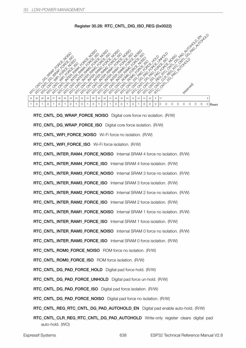
30. LOW-POWER MANAGEMENT
Register 30.28: RTC_CNTL_DIG_ISO_REG (0x0022)
RTC_C
NTL_D
G_WRAP_F
ORCE_NOIS
O
1
31
RTC_C
NTL_D
G_WRAP_F
ORCE_ISO
0
30
RTC_C
NTL_W
IFI_F
ORCE_NOIS
O
1
29
RTC_C
NTL_W
IFI_F
ORCE_ISO
0
28
RTC_C
NTL_IN
TER_R
AM4_
FORCE_N
OISO
1
27
RTC_C
NTL_IN
TER_R
AM4_
FORCE_IS
O
0
26
RTC_C
NTL_IN
TER_R
AM3_
FORCE_N
OISO
1
25
RTC_C
NTL_IN
TER_R
AM3_
FORCE_IS
O
0
24
RTC_C
NTL_IN
TER_R
AM2_
FORCE_N
OISO
1
23
RTC_C
NTL_IN
TER_R
AM2_
FORCE_IS
O
0
22
RTC_C
NTL_IN
TER_R
AM1_
FORCE_N
OISO
1
21
RTC_C
NTL_IN
TER_R
AM1_
FORCE_IS
O
0
20
RTC_C
NTL_IN
TER_R
AM0_
FORCE_N
OISO
1
19
RTC_C
NTL_IN
TER_R
AM0_
FORCE_IS
O
0
18
RTC_C
NTL_R
OM0_
FORCE_N
OISO
1
17
RTC_C
NTL_R
OM0_
FORCE_IS
O
0
16
RTC_C
NTL_D
G_PAD_F
ORCE_HOLD
0
15
RTC_C
NTL_D
G_PAD_F
ORCE_UNHOLD
1
14
RTC_C
NTL_D
G_PAD_F
ORCE_ISO
0
13
RTC_C
NTL_D
G_PAD_F
ORCE_NOIS
O
1
12
RTC_C
NTL_R
EG_RTC
_CNTL
_DG_P
AD_AUTO
HOLD_E
N
0
11
RTC_C
NTL_C
LR_R
EG_RTC
_CNTL
_DG_P
AD_AUTO
HOLD
0
10
RTC_C
NTL_D
G_PAD_A
UTOHOLD
0
9
(rese
rved)
0 0 0 0 0 0 0 0 0
17 9
Reset
RTC_CNTL_DG_WRAP_FORCE_NOISO Digital core force no isolation. (R/W)
RTC_CNTL_DG_WRAP_FORCE_ISO Digital core force isolation. (R/W)
RTC_CNTL_WIFI_FORCE_NOISO Wi-Fi force no isolation. (R/W)
RTC_CNTL_WIFI_FORCE_ISO Wi-Fi force isolation. (R/W)
RTC_CNTL_INTER_RAM4_FORCE_NOISO Internal SRAM 4 force no isolation. (R/W)
RTC_CNTL_INTER_RAM4_FORCE_ISO Internal SRAM 4 force isolation. (R/W)
RTC_CNTL_INTER_RAM3_FORCE_NOISO Internal SRAM 3 force no isolation. (R/W)
RTC_CNTL_INTER_RAM3_FORCE_ISO Internal SRAM 3 force isolation. (R/W)
RTC_CNTL_INTER_RAM2_FORCE_NOISO Internal SRAM 2 force no isolation. (R/W)
RTC_CNTL_INTER_RAM2_FORCE_ISO Internal SRAM 2 force isolation. (R/W)
RTC_CNTL_INTER_RAM1_FORCE_NOISO Internal SRAM 1 force no isolation. (R/W)
RTC_CNTL_INTER_RAM1_FORCE_ISO Internal SRAM 1 force isolation. (R/W)
RTC_CNTL_INTER_RAM0_FORCE_NOISO Internal SRAM 0 force no isolation. (R/W)
RTC_CNTL_INTER_RAM0_FORCE_ISO Internal SRAM 0 force isolation. (R/W)
RTC_CNTL_ROM0_FORCE_NOISO ROM force no isolation. (R/W)
RTC_CNTL_ROM0_FORCE_ISO ROM force isolation. (R/W)
RTC_CNTL_DG_PAD_FORCE_HOLD Digital pad force hold. (R/W)
RTC_CNTL_DG_PAD_FORCE_UNHOLD Digital pad force un-hold. (R/W)
RTC_CNTL_DG_PAD_FORCE_ISO Digital pad force isolation. (R/W)
RTC_CNTL_DG_PAD_FORCE_NOISO Digital pad force no isolation. (R/W)
RTC_CNTL_REG_RTC_CNTL_DG_PAD_AUTOHOLD_EN Digital pad enable auto-hold. (R/W)
RTC_CNTL_CLR_REG_RTC_CNTL_DG_PAD_AUTOHOLD Write-only register clears digital pad
auto-hold. (WO)
Espressif Systems 638 ESP32 Technical Reference Manual V2.8
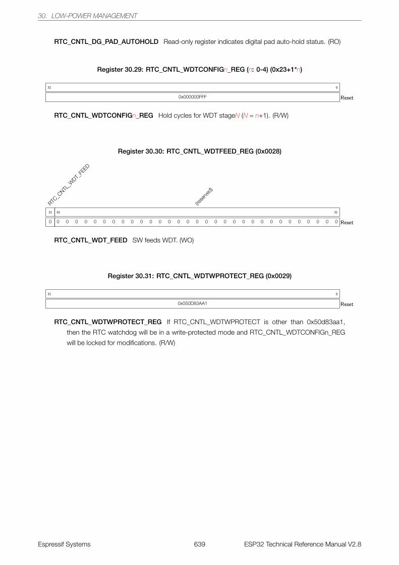
30. LOW-POWER MANAGEMENT
RTC_CNTL_DG_PAD_AUTOHOLD Read-only register indicates digital pad auto-hold status. (RO)
Register 30.29: RTC_CNTL_WDTCONFIGn_REG (n: 0-4) (0x23+1*n)
0x000000FFF
31 0
Reset
RTC_CNTL_WDTCONFIGn_REG Hold cycles for WDT stageN (N = n+1). (R/W)
Register 30.30: RTC_CNTL_WDTFEED_REG (0x0028)
RTC_C
NTL_W
DT_FE
ED
0
31
(rese
rved)
0 0 0 0 0 0 0 0 0 0 0 0 0 0 0 0 0 0 0 0 0 0 0 0 0 0 0 0 0 0 0
61 31
Reset
RTC_CNTL_WDT_FEED SW feeds WDT. (WO)
Register 30.31: RTC_CNTL_WDTWPROTECT_REG (0x0029)
0x050D83AA1
31 0
Reset
RTC_CNTL_WDTWPROTECT_REG If RTC_CNTL_WDTWPROTECT is other than 0x50d83aa1,
then the RTC watchdog will be in a write-protected mode and RTC_CNTL_WDTCONFIGn_REG
will be locked for modifications. (R/W)
Espressif Systems 639 ESP32 Technical Reference Manual V2.8
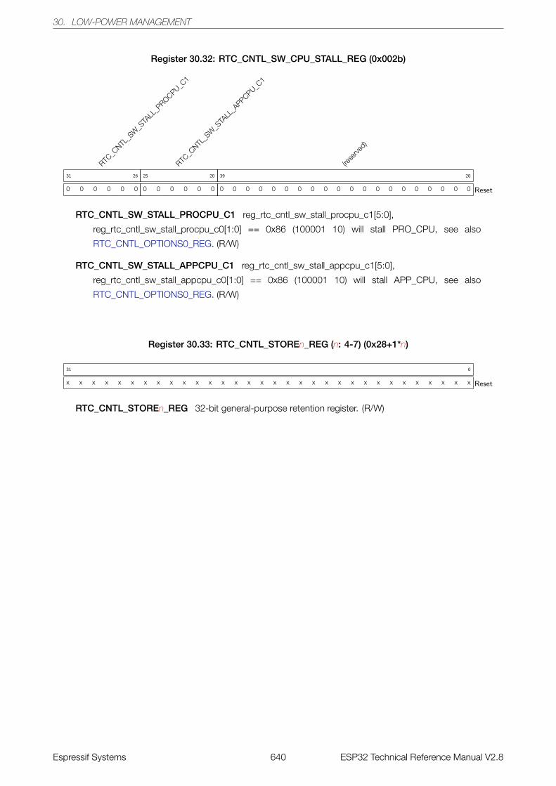
30. LOW-POWER MANAGEMENT
Register 30.32: RTC_CNTL_SW_CPU_STALL_REG (0x002b)
RTC_C
NTL_S
W_S
TALL
_PROCPU_C
1
0 0 0 0 0 0
31 26
RTC_C
NTL_S
W_S
TALL
_APPCPU_C
1
0 0 0 0 0 0
25 20
(rese
rved)
0 0 0 0 0 0 0 0 0 0 0 0 0 0 0 0 0 0 0 0
39 20
Reset
RTC_CNTL_SW_STALL_PROCPU_C1 reg_rtc_cntl_sw_stall_procpu_c1[5:0],
reg_rtc_cntl_sw_stall_procpu_c0[1:0] == 0x86 (100001 10) will stall PRO_CPU, see also
RTC_CNTL_OPTIONS0_REG. (R/W)
RTC_CNTL_SW_STALL_APPCPU_C1 reg_rtc_cntl_sw_stall_appcpu_c1[5:0],
reg_rtc_cntl_sw_stall_appcpu_c0[1:0] == 0x86 (100001 10) will stall APP_CPU, see also
RTC_CNTL_OPTIONS0_REG. (R/W)
Register 30.33: RTC_CNTL_STOREn_REG (n: 4-7) (0x28+1*n)
x x x x x x x x x x x x x x x x x x x x x x x x x x x x x x x x
31 0
Reset
RTC_CNTL_STOREn_REG 32-bit general-purpose retention register. (R/W)
Espressif Systems 640 ESP32 Technical Reference Manual V2.8
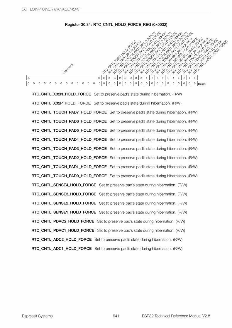
30. LOW-POWER MANAGEMENT
Register 30.34: RTC_CNTL_HOLD_FORCE_REG (0x0032)
(rese
rved)
0 0 0 0 0 0 0 0 0 0 0 0 0 0
31 18
RTC_C
NTL_X
32N_H
OLD_F
ORCE
0
17
RTC_C
NTL_X
32P_H
OLD_F
ORCE
0
16
RTC_C
NTL_T
OUCH_PAD7_
HOLD_F
ORCE
0
15
RTC_C
NTL_T
OUCH_PAD6_
HOLD_F
ORCE
0
14
RTC_C
NTL_T
OUCH_PAD5_
HOLD_F
ORCE
0
13
RTC_C
NTL_T
OUCH_PAD4_
HOLD_F
ORCE
0
12
RTC_C
NTL_T
OUCH_PAD3_
HOLD_F
ORCE
0
11
RTC_C
NTL_T
OUCH_PAD2_
HOLD_F
ORCE
0
10
RTC_C
NTL_T
OUCH_PAD1_
HOLD_F
ORCE
0
9
RTC_C
NTL_T
OUCH_PAD0_
HOLD_F
ORCE
0
8
RTC_C
NTL_S
ENSE4_HOLD
_FORCE
0
7
RTC_C
NTL_S
ENSE3_HOLD
_FORCE
0
6
RTC_C
NTL_S
ENSE2_HOLD
_FORCE
0
5
RTC_C
NTL_S
ENSE1_HOLD
_FORCE
0
4
RTC_C
NTL_P
DAC2_HOLD
_FORCE
0
3
RTC_C
NTL_P
DAC1_HOLD
_FORCE
0
2
RTC_C
NTL_A
DC2_HOLD
_FORCE
0
1
RTC_C
NTL_A
DC1_HOLD
_FORCE
0
0
Reset
RTC_CNTL_X32N_HOLD_FORCE Set to preserve pad’s state during hibernation. (R/W)
RTC_CNTL_X32P_HOLD_FORCE Set to preserve pad’s state during hibernation. (R/W)
RTC_CNTL_TOUCH_PAD7_HOLD_FORCE Set to preserve pad’s state during hibernation. (R/W)
RTC_CNTL_TOUCH_PAD6_HOLD_FORCE Set to preserve pad’s state during hibernation. (R/W)
RTC_CNTL_TOUCH_PAD5_HOLD_FORCE Set to preserve pad’s state during hibernation. (R/W)
RTC_CNTL_TOUCH_PAD4_HOLD_FORCE Set to preserve pad’s state during hibernation. (R/W)
RTC_CNTL_TOUCH_PAD3_HOLD_FORCE Set to preserve pad’s state during hibernation. (R/W)
RTC_CNTL_TOUCH_PAD2_HOLD_FORCE Set to preserve pad’s state during hibernation. (R/W)
RTC_CNTL_TOUCH_PAD1_HOLD_FORCE Set to preserve pad’s state during hibernation. (R/W)
RTC_CNTL_TOUCH_PAD0_HOLD_FORCE Set to preserve pad’s state during hibernation. (R/W)
RTC_CNTL_SENSE4_HOLD_FORCE Set to preserve pad’s state during hibernation. (R/W)
RTC_CNTL_SENSE3_HOLD_FORCE Set to preserve pad’s state during hibernation. (R/W)
RTC_CNTL_SENSE2_HOLD_FORCE Set to preserve pad’s state during hibernation. (R/W)
RTC_CNTL_SENSE1_HOLD_FORCE Set to preserve pad’s state during hibernation. (R/W)
RTC_CNTL_PDAC2_HOLD_FORCE Set to preserve pad’s state during hibernation. (R/W)
RTC_CNTL_PDAC1_HOLD_FORCE Set to preserve pad’s state during hibernation. (R/W)
RTC_CNTL_ADC2_HOLD_FORCE Set to preserve pad’s state during hibernation. (R/W)
RTC_CNTL_ADC1_HOLD_FORCE Set to preserve pad’s state during hibernation. (R/W)
Espressif Systems 641 ESP32 Technical Reference Manual V2.8
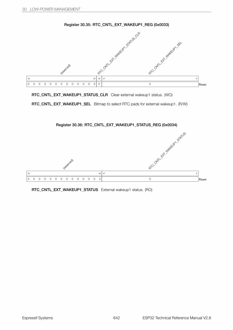
30. LOW-POWER MANAGEMENT
Register 30.35: RTC_CNTL_EXT_WAKEUP1_REG (0x0033)
(rese
rved)
0 0 0 0 0 0 0 0 0 0 0 0 0
31 19
RTC_C
NTL_E
XT_W
AKEUP1_STA
TUS_C
LR
0
18
RTC_C
NTL_E
XT_W
AKEUP1_SEL
0
17 0
Reset
RTC_CNTL_EXT_WAKEUP1_STATUS_CLR Clear external wakeup1 status. (WO)
RTC_CNTL_EXT_WAKEUP1_SEL Bitmap to select RTC pads for external wakeup1. (R/W)
Register 30.36: RTC_CNTL_EXT_WAKEUP1_STATUS_REG (0x0034)
(rese
rved)
0 0 0 0 0 0 0 0 0 0 0 0 0 0
31 18
RTC_C
NTL_E
XT_W
AKEUP1_STA
TUS
0
17 0
Reset
RTC_CNTL_EXT_WAKEUP1_STATUS External wakeup1 status. (RO)
Espressif Systems 642 ESP32 Technical Reference Manual V2.8
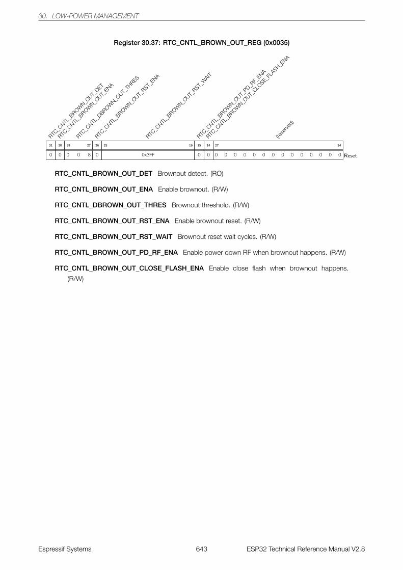
30. LOW-POWER MANAGEMENT
Register 30.37: RTC_CNTL_BROWN_OUT_REG (0x0035)
RTC_C
NTL_B
ROWN_O
UT_DET
0
31
RTC_C
NTL_B
ROWN_O
UT_ENA
0
30
RTC_C
NTL_D
BROWN_O
UT_TH
RES
0 0 8
29 27
RTC_C
NTL_B
ROWN_O
UT_RST_
ENA
0
26
RTC_C
NTL_B
ROWN_O
UT_RST_
WAIT
0x3FF
25 16
RTC_C
NTL_B
ROWN_O
UT_PD_R
F_ENA
0
15
RTC_C
NTL_B
ROWN_O
UT_CLO
SE_FLA
SH_ENA
0
14
(rese
rved)
0 0 0 0 0 0 0 0 0 0 0 0 0 0
27 14
Reset
RTC_CNTL_BROWN_OUT_DET Brownout detect. (RO)
RTC_CNTL_BROWN_OUT_ENA Enable brownout. (R/W)
RTC_CNTL_DBROWN_OUT_THRES Brownout threshold. (R/W)
RTC_CNTL_BROWN_OUT_RST_ENA Enable brownout reset. (R/W)
RTC_CNTL_BROWN_OUT_RST_WAIT Brownout reset wait cycles. (R/W)
RTC_CNTL_BROWN_OUT_PD_RF_ENA Enable power down RF when brownout happens. (R/W)
RTC_CNTL_BROWN_OUT_CLOSE_FLASH_ENA Enable close flash when brownout happens.
(R/W)
Espressif Systems 643 ESP32 Technical Reference Manual V2.8