Embed Size (px)
Citation preview

2014-6-20 EDSSC 2014 Chengdu 2
1、Introduction1.1 、Overview of ESD protection1.2 、ESD protection in Nanometer Process
2、ESD Protection in Nanometer Process2.1 、Diode 2.2 、Gate-Ground NMOS (GGNMOS)2.3、Silicon controlled Rectifier (SCR)
Outline

2014-6-20 EDSSC 2014 Chengdu 3
1、Introduction1.1 、Overview of ESD protection1.2 、ESD protection in Nanometer Process
2、ESD Protection in Nanometer Process2.1 、Diode 2.2 、Gate-Ground NMOS (GGNMOS)2.3、Silicon controlled Rectifier (SCR)
Outline

2014-6-20 EDSSC 2014 Chengdu 4
1、Introduction ESD destroy is main way of IC failure
With the processing developing, ESD is becoming serious problem!

2014-6-20 EDSSC 2014 Chengdu 5
1、Introduction ESD happens in anytime and any stage! So ESD protection should
be in IC whole lifetime.
Two ways to implement ESD protection according to different stages!
IC Fabricationin Fab
IC mount onPCB board
Custom using Produce with IC
On-board ESD Protection, such as TVS
On-Chip ESD protection, such as GGNMOS

(1)Transparent during IC working normally;
(2)During ESD happening,ESD protection circuit should:
Form a low resistance way by pass ESD current stress, so as to avoid ESD current stress flow into IC internal.
Clamp ESD voltage stress in some range to avoid overshoot!
So, How to designed ESD protection :
1、Introduction

(1)Current stress:
How ESD stress damage IC?
1、Introduction
For Example: 2KV HBM stress produce 0.91uJ heat, it can increase 160*1.2*5um MOS temperature to 2470℃, compared with Si melting Point 1415℃, Al’s 660℃!
Typical Failure: D-S silicon filament or metal interconnect melt due to joule heating

(2)Voltage stress:
How ESD stress damage IC?
1、Introduction
For example: Gate Oxide breakdown field E is 8-10 MV/cm. As to 0.18um/1.8V RF CMOS processing,its Gate Oxide breakdown voltage is below 4-5V,compared with human body recognized ESD voltage 3500V
Typical Failure: gate oxide films breakdown

ESD happen at every way, direction, place and time!
ESD should be designed carefully : robustness, Bi-direction, high open speed …
1、Introduction

2008-9-23 http://esd.iclab.cn /6810
1、Introduction

2014-6-20 EDSSC 2014 Chengdu 11
1、Introduction1.1 、Overview of ESD protection1.2 、ESD protection in Nanometer Process
2、ESD Protection in Nanometer Process2.1 、Diode 2.2 、Gate-Ground NMOS (GGNMOS)2.3、Silicon controlled Rectifier (SCR)
Outline

2008-9-23 http://esd.iclab.cn /6812
For Example: most of ESD destroy in 40nm process is gate breakdown
HBM ESD Failure
MM ESD Failure
CDM ESD Failure
1、Introduction

2008-9-23 http://esd.iclab.cn
1、Introduction
BV decreased with its gate thinner;
BV decreased with the channel length shrink;
BV is lowest when the gate area and channel length meet the smallest of design ruler;
Key(1): Gate breakdown voltage(BV) decreased with the process developing
Data from ESD Lab of Zhejiang University

2014-6-20 EDSSC 2014 Chengdu 14
Metal L DC Rdc Voltage drop under 2KV HBM
Rate/40nmI/O 2.5V
Rate/28nmI/O1.8V
50um 0.91Ω 0.18V 6% 8.3%100um 1.83Ω 0.37V 14.8% 20.5%300um 1.83Ω 1.11 V 44.4% 61.7%
WTLRmetalρ
=
Vi/o= Iesd * (Ron + Rvdd + Rvss + Rpc)+Vpc+Von
1、IntroductionKey(2): With the process development, voltage drop on the interconnect increased while IC working voltage drop. So The rate of drop of interconnect become obvious!
Data from ESD Lab of Zhejiang University

2008-9-23 http://esd.iclab.cn /6815
Key(3): ESD design windows shrinks obviously! Especially, ESD devices clamp voltage under avalanche breakdown
working state.
1、Introduction
Data from TI

2008-9-23 http://esd.iclab.cn /6816
0 2 4 6 8 10 12 14
20% Safty Margin
20% Safty Margin
20% Safty Margin
10.5V3V
7.4V2.2V
Voltage (V)
Cur
rent
40nm IO ESD Window
28nm IO ESD Window
0 2 4 6
20% Safty Margin
5V1.3V
Voltage (V)
Cur
rent
28nm Core ESD Window
20% Safty Margin
40nm Process and 28nm Process ESD design windows
1、Introduction
Data from ESD Lab of Zhejiang University
ESD design wondows in Foundry

2014-6-20 EDSSC 2014 Chengdu 17
1、Introduction1.1 、Overview of ESD protection1.2 、ESD protection in Nanometer Process
2、ESD Protection in Nanometer Process2.1 、Diode 2.2 、Gate-Ground NMOS (GGNMOS)2.3、Silicon controlled Rectifier (SCR)
Outline
2008-9-23 http://esd.iclab.cn /6818
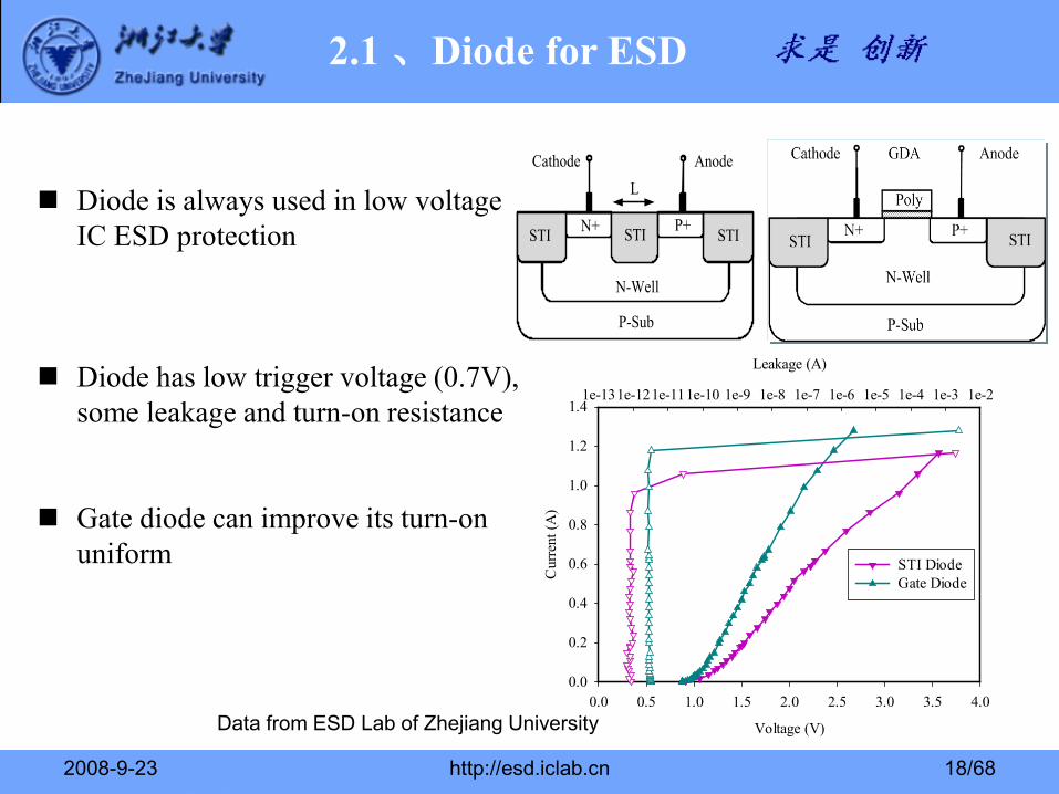
Diode is always used in low voltage IC ESD protection
Diode has low trigger voltage (0.7V), some leakage and turn-on resistance
Gate diode can improve its turn-on uniform
2.1 、Diode for ESD
Voltage (V)
0.0 0.5 1.0 1.5 2.0 2.5 3.0 3.5 4.0
Cur
rent
(A)
0.0
0.2
0.4
0.6
0.8
1.0
1.2
1.4
Leakage (A)
1e-131e-121e-111e-10 1e-9 1e-8 1e-7 1e-6 1e-5 1e-4 1e-3 1e-2
STI DiodeGate Diode
STI STIP+N+
N-Well
P-Sub
AnodeCathode
STI
L
Data from ESD Lab of Zhejiang University

2008-9-23 http://esd.iclab.cn /6819
Poly
AnodeCathode
P+N+
N-Well
P-Sub
GDA
STI STI
Poly
AnodeCathode
P+N+
N-Well
P-Sub
GDB
STI STI
Poly
AnodeCathode
P+N+
N-Well
P-Sub
GDC
STI STI
Poly
AnodeCathode
P+N+
P-Well
P-Sub
GDD
STI STI
Poly
AnodeCathode
P+N+
P-Well
P-Sub
GDE
STI STI
Voltage (V)0.0 0.5 1.0 1.5 2.0 2.5 3.0 3.5 4.0
Cur
ent (
A)
0.0
0.2
0.4
0.6
0.8
1.0
Leakage (A)
1e-8 1e-7 1e-6 1e-5 1e-4 1e-3 1e-2 1e-1 1e+0
GDDGDE
Voltage (V)0.0 0.5 1.0 1.5 2.0 2.5 3.0 3.5 4.0 4.5
Cur
rent
(A)
0.0
0.2
0.4
0.6
0.8
1.0
Leakage (A)1e-10 1e-9 1e-8 1e-7 1e-6 1e-5 1e-4 1e-3 1e-2 1e-1 1e+0
GDAGDBGDC
2.1 、Diode for ESD
Data from ESD Lab of Zhejiang University
Different kind of Gate diode TLP curves

2008-9-23 http://esd.iclab.cn /6820
Anode
Cathode
Ie1
Ib3
N+
P-Sub
N+ P+P+N+ P+
NWNWNW
AnodeCathode
P+
GND
Q1Q2Q3
Q1
Q1
Q1
Diodes in series can meet different voltage demand.
Owing to Darlington effect, the leakage will increase and voltage increasing will be weaken with the number of Diodes in series.
It can be improved by retrograde well process
2.1 、Diode for ESD
Data from ESD Lab of Zhejiang University

2014-6-20 EDSSC 2014 Chengdu 21
1、Introduction1.1 、Overview of ESD protection1.2 、ESD protection in Nanometer Process
2、ESD Protection in Nanometer Process2.1 、Diode 2.2 、Gate-Ground NMOS (GGNMOS)2.3、Silicon controlled Rectifier (SCR)
Outline

2008-9-23 http://esd.iclab.cn /6822
P+
Anode Cathode
N+
P-SUB
N+
L
W
DCP SCP
GGNMOS is widely applied in IC ESD protection owing to its simple structure!
GGNMOS key structure parameters: channel width (W), channel length (L), drain contact to ploy (DCP) and source contact to ploy (SCP)
2.2、GGNMOS for ESD

2014-6-20 EDSSC 2014 Chengdu 23
TLP results of GGNMOS in 65nm CMOS process with different W & L
2.2、GGNMOS for ESD
Data from ESD Lab of Zhejiang University

2014-6-20 EDSSC 2014 Chengdu 24
Design ruler : (different from deep-sub-micro process ESD protection)
The key of the 40nm process ESD are very narrow ESD window and low BV of thin oxide thickness. The W, effected on trigger voltage and holding voltage, should be mainly consider. L is no longer the main factor to affect the failure current.
90nm and 65nm process: the W mainly effect on the uniformity of current. Small L will achieve an excellent failure current, while it also has low holding voltage. Setting L should be trade off.
DCP increasing will improve current uniformity so as to increase It2, because of DCP as a ballast resistor. The best DCP for ESD protection is different under different process. SCP is minor compared to DCP
Both DCP & SCP have a little effect on the trigger voltage and holding voltage.
2.2、GGNMOS for ESD

2008-9-23 http://esd.iclab.cn /6825
GGNMOS can be used in 90nm &65nm, even 45nm process, but it totally can not be used in 28nm process owing to its very high trigger and bad clamp ability!
TLP results of GGNMOS in 40&28nm CMOSVoltage (A)
-2 0 2 4 6 8 10
()
0.0
0.2
0.4
0.6
0.8
1.0
1.2
1.4
1.640nm GGNMOS 28nm GGNMOS
Zoom in
4 5 6 7 8 90.000
0.003
0.006
0.009
0.012
0.015
0.018
2.2、GGNMOS for ESD

2014-6-20 EDSSC 2014 Chengdu 26
PMOS
(a)
P+ N+Poly
N+
P_Well
P+ P+ N+
N_Well
VDD
P+Poly
I/O PAD
(b)
Itri
SAB
P+N+ Poly
N+
Itri
N+
N_Well
N+
N_Well
Rsub Rsub
Rsub
Main NMOS
VSS
I/O PAD Core Circuit
RVSS
PowerClamp
RVSS
RVDD RVDDVDD
P_Sub
S. Dong, etl, Substrate-engineered GGNMOS for low trigger voltage ESD in 65nm CMOS process, Microelectronics Reliability, Volume 51, Issue 12, December 2011, Pages 2124-2128.
Two kinds of modified GGNMOS for low trigger
Substrate R and I trigger GGNMOS Substrate R trigger GGNMOS
2.2、GGNMOS for ESD

2014-6-20 EDSSC 2014 Chengdu 27
It2(A) Vt1(V) C(pF) It2/area (mA/um2)
GGNMOS 2.13 6.84 0.652 2.5Substrate R trigger GGNMOS 2.07 5.3 0.788 2.17Substrate R and I trigger GGNMOS 2.63 3 0.891 2.33
Substrate R and I trigger GGNMOS Substrate R trigger GGNMOS
(1)Substrate-engineered GGNMOS for low trigger
2.2、GGNMOS for ESD

2014-6-20 EDSSC 2014 Chengdu 28
1、Introduction1.1 、Overview of ESD protection1.2 、ESD protection in Nanometer Process
2、ESD Protection in Nanometer Process2.1 、Diode 2.2 、Gate-Ground NMOS (GGNMOS)2.3、Silicon controlled Rectifier (SCR)
Outline

2008-9-23 http://esd.iclab.cn /6829Voltage (V)
0 2 4 6 8 10 12
Cur
rent
(A)
0.0
0.2
0.4
0.6
0.8
1.0
Leakage (A)
1e-131e-121e-111e-10 1e-9 1e-8 1e-7 1e-6 1e-5 1e-4 1e-3 1e-2
28nm Normal SCR
STISTI STIN+P+
N-Well
P-Sub
Cathode
RP-Well
STIN+P+
P-Well
STI
RN-Well
Anode
QNQP
SCR is a excellent choice for 40&28 nm process ESD protection.
2.3、SCR for ESD

2008-9-23 http://esd.iclab.cn /6830Voltage (V)
0 2 4 6 8 10 12
Cur
rent
(A)
0.0
0.2
0.4
0.6
0.8
1.0
Leakage (A)
1e-131e-121e-111e-10 1e-9 1e-8 1e-7 1e-6 1e-5 1e-4 1e-3 1e-2
28nm Normal SCR
N+N+
NW
P-Sub
N+ P+ N+N+P+ P+ P+ P+N+
PWNWNW
Anode CathodeCathode
Voltage (V)0 1 2 3 4 5 6 7 8
0.0
0.2
0.4
0.6
0.8
1.0
1.2
1.4
1.6
Leakage (A)1e-7 1e-6 1e-5 1e-4 1e-3 1e-2 1e-1
TD-DTSCR
1.2 1.3 1.4 1.5 1.6 1.7 1.8 1.9 2.00.00
0.02
0.04
0.06
0.08
0.10
Zoom in
SCR triggered by diode (DTSCR) has a lower trigger voltage
2.3、SCR for ESD

2014-6-20 EDSSC 2014 Chengdu 31
Structures Area /μm2 Vt1 /V It2 /A CESD /fF Ileak /nA
GGNMOS 17*50 7.3 2.13 652 0.9
LVTSCR 6*50 7.5 1.82 130 0.35
DTSCR 12*50 2.5 1.93 96 120
ILVTSCR 9*50 2.2 1.9 50 0.3
2.3、SCR for ESD

2014-6-20 EDSSC 2014 Chengdu 32
P-well
P+N+
N-well
Anode
N+P+P+N+N+
CathodeGate
P-sub (c)
(a)
I/O
R_nw
R_pw
C1
C2
C3
C5
C4
Q1
Q2 M1
VSS
Anode
Cathode
C1
C3 C4
(b)
C2 C5
P-well
P+N+
N-well
N+P+P+N+N+
Gate
P-Sub
P-well
P+
Nw P-well
N+
CathodeAnode
R_sub (c)
I/O
(a)
RgR_sub
trigger path
Dio
de p
ath
C2
C1
VSS
Q1Q2 M1
D1
C5
R_nw
C6
C4C3
Anode
Cathode
C1
C6 C2 C3
(b)
C4 C5
Improved LVTSCR (ILVTSCR)LVTSCRS. Dong, "Improved Low-Voltage-Triggered SCR Structure for RF-ESD Protection," Electron Device Letters, IEEE , vol.34, no.8, pp.1050,1052, Aug. 2013.
Improved LVTSCR for low trigger and low capacitance (ILVTSCR)
2.3、SCR for ESD

2014-6-20 EDSSC 2014 Chengdu 33
Floating P+ LVTSCR for high holding voltage has two snapback with high It2
S. Dong, “Design and Analysis of an Area-efficient High Holding Voltage ESD Protection Device,“ IEEE Transaction on Electron Device, 2015,1
2.3、SCR for ESD

2014-6-20 EDSSC 2014 Chengdu 34 34
Improved Diode trigger SCR with two snapback meet 2V ESD design windows
S. Dong, "Minimizing Multiple Triggering Effect in Diode-Triggered Silicon Controlled Rectifier (SCR) for ESD Protection Applications,“ IEEE Electron Device Lett.,2012,11
2.3、SCR for ESD

END
Thanks!
2008-9-23 http://esd.iclab.cn /6835


![P087 Reliability Modeling on 90 nm n-channel MOSFETs with ...€¦ · [6] E. Maricau and G. Gielen,Analog IC Reliability in Nanometer CMOS,Springer Science Business Media New](https://img.dokumen.tips/doc/110x75/5fb67b16ce590245f2046e91/p087-reliability-modeling-on-90-nm-n-channel-mosfets-with-6-e-maricau-and.jpg)