Embed Size (px)
Citation preview

February 2012 Altera Corporation
ES-01022-6.1 Errata Sheet
© 2012 Altera Corporation. All rights reserved. ALTERA, ARRIA, CYCLONE, HARDCOPY, MAX, MEGACORE, NIOS, QUARTUS and STRATIX words and logos are trademarks of Altera Corporation and registered in the U.S. Patent and Trademark Office and in other countries. All other words and logos identified as trademarks or service marks are the property of their respective holders as described at www.altera.com/common/legal.html. Altera warrants performance of its semiconductor products to current specifications in accordance with Altera's standard warranty, but reserves the right to make changes to any products and services at any time without notice. Altera assumes no responsibility or liability arising out of the application or use of any information, product, or service described herein except as expressly agreed to in writing by Altera. Altera customers are advised to obtain the latest version of device specifications before relying on any published information and before placing orders for products or services.
101 Innovation DriveSan Jose, CA 95134www.altera.com
Subscribe
ISO 9001:2008 Registered
Errata Sheet for Stratix IV GX Devices
This errata sheet provides updated information about known device issues affecting Stratix® IV GX devices.
Production Device Issues for Stratix IV GX DevicesTable 1 lists the issues and affected Stratix IV GX production devices..
Table 1. Production Device Issues for Stratix IV GX Devices (Part 1 of 2)
Issue Affected Devices Planned Fix
“PLL phasedone Signal Stuck at Low”
In some cases, the Stratix IV phase-locked loop (PLL) blocks exhibit the phasedone signal stuck at low during the PLL dynamic phase shift.
All Stratix IV GX(ES and Production)
Devices
Quartus II software version 12.0 and later.
“Remote System Upgrade”
The remote system upgrade feature fails when loading an invalid configuration image.
All Stratix IV GX(ES and Production)
Devices
Quartus II software version 9.1 and later.
“EDCRC False Errors”
The error detection CRC (SEU detection) feature may falsely assert the CRC_ERROR signal when no SEU event has occurred.
All Stratix IV GX(ES and Production)
Devices—
“PCI Express (PCIe) Gen2 Protocol Link Establishment Issue”
The PCIe rate switch controller may not be initialized correctly for the PCIe Gen2 protocol, preventing the link from being established.
All Stratix IV GX(ES and Production)
Devices
Quartus II software version 10.1 SP1 and later.
Patches are available for the Quartus II software versions
9.1 SP2 and 10.1.
“Quartus II Software Incorrect Setting for Transceiver CDR in All Modes Except PCIe Mode”
The Quartus II software incorrectly sets the CDR unit when the transceiver channel is configured in any mode except PCIe mode and the CDR is configured to automatic lock mode.
All Stratix IV GX(ES and Production)
Devices
Quartus II software version 10.1 and later.
Patches are available for the Quartus II software versions
9.1 SP2 and 10.0 SP1.
“Dynamic Reconfiguration Issue Between PCIe Mode and Any Other Transceiver Mode”
The transceiver may not be initialized correctly if your application uses dynamic reconfiguration to change the transceiver channel between PCIe mode and any other transceiver mode.
All Stratix IV GX (ES and Production)
Devices
No plan to fix silicon. Apply the reset sequence in
“Dynamic Reconfiguration Issue Between PCIe Mode and Any Other Transceiver
Mode”.
“Quartus II Mapping Issue with PCIe Interfaces Using the Hard IP Block”
The Quartus II software incorrectly maps the PCIe interfaces when using the hard IP block.
All Stratix IV GX (ES and production) devices
For more information, refer to “Quartus II Mapping Issue with PCIe Interfaces Using
the Hard IP Block”

Page 2 Production Device Issues for Stratix IV GX Devices
February 2012 Altera Corporation Errata Sheet for Stratix IV GX Devices
“I/O Jitter”
Affected Stratix IV GX production devices may exhibit higher than expected jitter on general purpose I/O pins.
EP4SGX70, EP4SGX110, EP4SGX290, EP4SGX360, EP4SGX530
EP4SGX70 Rev B, EP4SGX110 Rev B, EP4SGX290 Rev B, EP4SGX360 Rev B, EP4SGX530 Rev E
“Fast Passive Parallel Mode Configuration Failures at High DCLK Frequency”
Stratix IV GX configuration fails in FPP mode when the DCLK frequency is set to 125 MHz with a 60/40 or 40/60 duty cycle.
All production devices —
“FPP Mode Configuration Failures When the Minimum Hold Time (tDH) is set to 0 ns or 24 ns”
Stratix IV GX configuration fails in FPP mode when the minimum data hold time (tDH) is set to 0 ns for uncompressed and unencrypted configuration data or 24 ns for compressed and/or encrypted data.
All production devices —
“Transmitter PLL Lock (pll_locked) Status Signal”
The transmitter PLL lock status signal (pll_locked) does not deassert when the pll_powerdown signal is asserted in configurations that use the reference clock pre-divider of 2, 4, or 8.
All Stratix IV GX (ES and production) devices
No plan to fix silicon. For a soft-fix solution, refer to “Transmitter PLL Lock (pll_locked) Status Signal”
“M144K RAM Block Lock-Up”
M144K RAM blocks may lock up if there is a glitch in the clock source.
All production devices —
“x8 and xN Clock Line Timing Issue for Transceivers”
xN clock line performance limits data rates depending on clock source configuration.
All production devices —
“Stratix IV GX Power-up Sequencing on Production Devices”
The device fails to power up and exit POR at low temperatures when VCC is powered after VCCAUX.
All production devices —
“Higher Power Supply Current During Power-Up for VCCPD and VCCA_L/R”
Higher power-up current requirements are needed for VCCPD and VCCA_L/R power supplies.
All Stratix IV GX (ES and production) devices
Refer to “Higher Power Supply Current During Power-Up for VCCPD and VCCA_L/R” on page 22
Table 1. Production Device Issues for Stratix IV GX Devices (Part 2 of 2)
Issue Affected Devices Planned Fix

Production Device Issues for Stratix IV GX Devices Page 3
February 2012 Altera CorporationErrata Sheet for Stratix IV GX Devices
PLL phasedone Signal Stuck at LowIn some cases, the Stratix IV PLL blocks exhibit the phasedone signal stuck at low during the PLL dynamic phase shift. When the PLL phasedone signal is stuck at low, the intended phase shift does not happen. You can recover from the PLL phasedone signal being stuck at low by resetting the PLL or by restarting the phase shift operation by asserting the phasestep signal.
SolutionTo resolve the PLL phasedone signal stuck at low issue, the Altera PLL megafunction is enhanced to automatically restart the phase shift operation internally in the Altera PLL megafunction whenever the PLL phasedone signal is stuck at low. Restarting the phase shift operation compensates for the missing phase shift operation and also recovers the phasedone signal.
This Altera PLL megafunction solution will be implemented in the Quartus II software version 12.0 and later. Altera recommends upgrading to the latest Quartus II software, regenerating the PLL megafunction, and recompiling your design.
Additionally, software patches are available for the Quartus II software versions 9.1 SP2 and 10.1 SP1 to upgrade the PLL megafunction with the solution. To download and install the Quartus II software patch, refer to the PLL Phasedone Stuck at Low Solution.
If you need additional support, file a service request using mySupport.
Remote System UpgradeThe remote system upgrade feature does not operate correctly when you initiate a reconfiguration cycle that goes from a factory configuration image to an invalid application configuration image. In this scenario, the device fails to revert back to the factory configuration image after a configuration error is detected while loading the invalid application configuration image. The failure is indicated by a continuous toggling of the nSTATUS pin.
In correct operation, the device reverts to the factory configuration image after a configuration error is detected with the invalid configuration image.
1 An invalid application configuration image is classified as one of the following:
■ A partially programmed application image
■ A blank application image
■ An application image assigned with a wrong start address
The remote system upgrade feature works correctly with all other reconfiguration trigger conditions.
This issue is addressed by enabling the Reconfig POF Checking feature in the updated ALTREMOTE_UPDATE megafunction and is available in the Quartus® II software version 9.1 and later.
f For more information about how to enable the Reconfig POF Checking feature, refer to AN 603: Active Serial Remote System Upgrade Reference Design.

Page 4 Production Device Issues for Stratix IV GX Devices
February 2012 Altera Corporation Errata Sheet for Stratix IV GX Devices
EDCRC False ErrorsThe error detection cyclic redundancy check (CRC) (single event upset [SEU] detection) feature may falsely assert the CRC_ERROR signal when no SEU event has occurred. This falsely asserted CRC_ERROR signal happens because the configuration RAM is incorrectly read for the EDCRC checks. In this scenario, the configuration RAM data and the functionality of the device are not affected.
■ If EDCRC is not critical to your system, turn it off.
■ If EDCRC is required, insert a soft IP in your design.
f For more support and to request the soft IP, file a service request using mySupport.
PCI Express (PCIe) Gen2 Protocol Link Establishment IssueThe PCI Express® (PCIe®) rate switch controller may not be initialized correctly for the PCIe Gen2 protocol, preventing the link from being established. When the rate switch controller is not initialized correctly, the transmitted TS1 training sequence is corrupted. This link establishment issue occurs intermittently and in some cases, power cycling the device may re-establish the link. This link establishment issue affects PCIe Gen2 x1, x4, and x8 configurations with and without the hard IP block. The PCIe Gen1 only configurations are not affected.
SolutionThe issue is fixed in the Quartus II software versions 10.1 SP1 and later. Altera recommends upgrading to the latest Quartus II software, regenerating the IP, and recompiling your design. For complete details of the solution, refer to the PCIe Gen2 Protocol Link Solution.
Additionally, software patches are available for the Quartus II software versions 9.1 SP2 and 10.1.
f To download and install the patch, refer to the PCIe Gen2 Protocol Link Solution.
Quartus II Software Incorrect Setting for Transceiver CDR in All Modes Except PCIe Mode
The Quartus II software versions 10.0 SP1 and earlier incorrectly set the clock and data recovery (CDR) unit when the transceiver channel is configured in any mode except PCIe mode and the CDR is configured to automatic lock mode. When there are no data transitions on the transceiver data inputs for an extended period of time (in the ms range), the CDR may keep the rx_freqlocked signal asserted. The CDR does not return to the lock-to-reference state and incorrect data may be recovered.
1 The transceiver channels configured in PCIe mode are NOT affected by this issue.
Solution This setting issue is fixed in the Quartus II software versions 10.1 and later. Altera recommends upgrading to the latest Quartus II software and recompiling your design. For complete details of the solution, refer to the Transceiver CDR Solution.

Production Device Issues for Stratix IV GX Devices Page 5
February 2012 Altera CorporationErrata Sheet for Stratix IV GX Devices
Additionally, software patches are available for the Quartus II software versions 9.1 SP2 and 10.0 SP1.
f To download and install the patch, refer to the Transceiver CDR Solution.
f If you need additional support, file a service request using Altera’s mysupport.
Dynamic Reconfiguration Issue Between PCIe Mode and Any Other Transceiver Mode
If your application uses dynamic reconfiguration to change the transceiver channel between PCIe mode and any other transceiver mode, the transceiver may not be initialized correctly, resulting in receiver bit errors.
1 This dynamic reconfiguration issue affects dynamic reconfiguration between PCIe mode and any other transceiver mode only. Dynamic reconfiguration between any transceiver modes other than PCIe mode is not affected.
Workaround
f If you see bit errors, apply the reset sequence described in the Reset Sequence Solution.
f If you need additional support, file a service request using Altera’s mysupport.
Quartus II Mapping Issue with PCIe Interfaces Using the Hard IP BlockThe Quartus II software versions 9.1, 9.1 SP1, and 9.1 SP2 incorrectly allow logical channel 0 to be placed in any physical channel for x1 and x4 PCIe Gen1 interfaces with the hard IP block. For correct operation with the hard IP block, logical channel 0 must be placed in physical channel 0.
This mapping issue is fixed in the Quartus II software version 10.0; however, Altera recommends upgrading to the Quartus II software version 10.0 SP1. If you have already designed or fabricated your boards using the incorrect mapping, for assistance to remedy this problem, file a service request using mySupport.
I/O JitterAffected Stratix IV GX production devices (refer to Table 1 on page 1) may exhibit up to ± 50 ps higher than expected jitter on general purpose I/O pins. Transceiver I/O pins and I/O pins in LVDS mode (including dynamic phase alignment [DPA] and soft CDR) are not affected. The actual amount of additional jitter depends on the device switching activity.
The EP4SGX180 and EP4SGX230 production ordering codes are not affected.
Altera is fixing this issue in the next revision of production devices, which will meet all current jitter specifications.
f For further support, file a service request using mySupport.

Page 6 Production Device Issues for Stratix IV GX Devices
February 2012 Altera Corporation Errata Sheet for Stratix IV GX Devices
Fast Passive Parallel Mode Configuration Failures at High DCLK FrequencyStratix IV GX devices might fail to configure in FPP mode if the DCLK frequency is set to 125 MHz with a 60/40 or 40/60 duty cycle. When this configuration issue occurs, the device pulls the nSTATUS pin low and the configuration host may initiate a reconfiguration.
This problem affects all Stratix IV GX devices.
For successful FPP configuration at 125 MHz for devices with the density of the EP4SGX360 and lower (except for the EP4SGX360 F1932 and EP4SGX290 F1932 packages), set the duty cycle to 45/55, 55/45, or higher. This setting corresponds to a minimum DCLK high time (tCH) and a minimum DCLK low time (tCL) of 3.6 ns.
For EP4SGX530, EP4SGX360 F1932, and EP4SGX290 F1932 devices, reduce the DCLK frequency to 100 MHz or lower and set the duty cycle to 45/55, 55/45, or higher. This setting corresponds to a minimum DCLK high time (tCH) and a minimum DCLK low time (tCL) of 4.5 ns.
FPP Mode Configuration Failures When the Minimum Hold Time (tDH) is set to 0 ns or 24 ns
Stratix IV GX devices might fail to configure in FPP mode if the minimum hold time (tDH) for the configuration data is set to 0 ns for uncompressed and unencrypted configuration data, or 24 ns for compressed and/or encrypted data. When this configuration issue occurs, the device pulls the nSTATUS pin low and the configuration host may initiate a reconfiguration.
This problem affects all Stratix IV GX devices.
You can successfully configure the Stratix IV GX devices in FPP mode by setting the minimum hold time (tDH) for the uncompressed and unencrypted configuration data to 1 ns or higher. For compressed and/or encrypted data, set the minimum hold time (tDH) to 3 * 1/fDCLK + 1 ns or higher (fDCLK is your DCLK frequency setting). Alternatively, you can drive the configuration data out on the falling edge of the DCLK.
1 The MAX II Parallel Flash Loader drives out configuration data on the falling edge of the DCLK. This issue does not affect you if you use the Max II Parallel Flash Loader as the configuration controller.

Production Device Issues for Stratix IV GX Devices Page 7
February 2012 Altera CorporationErrata Sheet for Stratix IV GX Devices
Transmitter PLL Lock (pll_locked) Status SignalThe transmitter PLL lock status signal (pll_locked) does not deassert when the pll_powerdown signal is asserted in configurations that use the reference clock pre-divider of 2, 4, or 8. Figure 1 shows the reference clock pre-divider inside transmitter PLLs. This transmitter PLL lock status signal issue impacts the pll_locked status signal in both the CMU PLL and the ATX PLL.
f Designs that implement the recommended transceiver reset sequence described in the Reset Control and Power Down chapter in volume 2 of the Stratix IV Device Handbook could potentially see a link failure after coming out of reset.
You can determine whether the Transmitter PLL in your design uses a reference clock pre-divider of 2, 4, or 8 by referring to the Quartus II software Compilation Report. Figure 2 shows an example of the GXB Transmitter PLL report, which you find in the “Resources Section” under “Fitter” in the Compilation Report. If the value in the Divide By column reads 2, 4or 8, your design is impacted by the pll_locked status signal issue.
Figure 1. Reference Clock Pre-Dividers in Transmitter PLLs
/1, /2, /4, /8Input Reference
Clock
Reference ClockPre-Divider
CMU/ATX PLL
CMU0High-Speed
Clock
Charge Pump+
Loop FilterPFD /L
/M
VCO
pll_lockedLockDetect
Figure 2. Determining Reference Clock Pre-Divider Value in the Compilation Report

Page 8 Production Device Issues for Stratix IV GX Devices
February 2012 Altera Corporation Errata Sheet for Stratix IV GX Devices
If the pll_locked issue impacts your design, instantiate and connect the pll_locked_soft_logic module, as shown in Figure 3. Use the pll_locked_to_corelogic output from this module in the transceiver reset logic and any user logic that relies on the transmitter PLL lock status signal.
Click pll_locked_soft_logic to obtain the module.
1 Use the calibration block clock (cal_blk_clk) for the pll_locked_soft_logic module. The cal_blk_clk frequency specification ranges from 10 MHz to 125 MHz. Depending on your cal_blk_clk frequency, set the parameter p_delay_counter in the pll_locked_soft_logic so that the delay is equal to 100 μs (worst-case transmitter PLL lock time).
M144K RAM Block Lock-UpM144K blocks may lock up if there is a glitch in the clock source when rden equals 1. In the lock-up state, the RAM block does not respond to read or write operations and requires an FPGA reconfiguration to restore operation. The block lock-up issue occurs within the M144K RAM in the Read Timer Trigger circuitry. A clock glitch may inadvertently freeze the Read Timer Trigger circuitry, locking the RAM block in its last operation. MLABs and M9K RAM blocks are not affected.
The workaround is to add clock-enable logic, an internal PLL, or clock-generation logic (for example, a clock divider). You can add clock-enable logic (internal or external) to disable the RAM block operation until the clock is stable. You can also gate the clock internally or externally. If FPGA resources permit, you can use an internal PLL or clock-generation logic to ensure a stable clock source at the RAM block input.
The Read Timer circuitry makes RAM block operation independent of the input clock duty cycle, thus maximizing design performance. If you cannot provide a stable clock, use the DCD option in the Quartus II software version 9.1 to work around this problem. When the M144K block uses the DCD option, it does not exhibit the lock-up behavior, but clock high-time requirements are increased and fMAX performance is degraded.
Figure 3. Instantiating and Connecting the pll_locked_soft_logic Module
top_cal_blk_clk
top_pll_inclk
pll_powerdown
tx_digitalreset
xcvr_async_reset
system_clk
xcvr_async_reset
clk
pll_locked
inst3
xcvr_reset_logic
inst2
pll_locked_soft_logic
serdes_io
inst
pll_locked[0..0]
tx_clkout[0..0]
tx_dataout[0..0] top_tx_dataout
cal_blk_clk
tx_datain[39..0]tx_datain[39..0]
tx_digitalreset[0..0]
pll_inclk
pll_powerdown[0..0]
pll_locked_to_corelogicclk
reset
pll_locked_from_altgx
Production Device Issues for Stratix IV GX Devices Page 9
February 2012 Altera CorporationErrata Sheet for Stratix IV GX Devices
If you cannot provide a stable clock input without glitches, to enable the DCD option in the Quartus II software, perform the following steps:
1. On the Assignments menu, click Settings.
2. In the Category list, select Fitter Settings.
3. Click More Settings.
4. Under Existing option settings, set M144K Block Read Clock Duty Cycle Dependency to On.
5. Click OK.
6. Compile your design.
Use the .qsf variable instead of the previous instructions for making a global assignment.
DCD is on globally by adding the following line to the project’s .qsf (the default is Off):
set_global_assignment -name M144K_BLOCK_READ_CLOCK_DUTY_CYCLE_DEPENDENCY ON
Alternatively, you can also apply this setting to individual M144K blocks with the Assignment Editor.
Global and per instance assignments can be mixed. For example, you can set DCD to On globally, but set it to Off for an instance. You can also set it to On for an instance.
x8 and xN Clock Line Timing Issue for TransceiversThe xN clock line timing issue in Stratix IV GX production devices affects the maximum data rate supported in the following transceiver configurations:
■ Basic x8 functional mode using CMU PLL or ATX PLL (6G)
■ Basic x1 and Basic x4 functional mode using ATX PLL (6G)
■ Basic (PMA Direct) xN functional mode using CMU PLL or ATX PLL (6G)
■ (OIF) CEI PHY Interface functional mode using ATX PLL (6G)
The maximum supported data rate in these configurations depends on:
■ Transmitter PLL type (CMU PLL or ATX PLL [6G])
■ Device speed grade
■ VCCL_GXB/VCCT/VCCR power supply level
1 The voltage supply levels can be 1.1 V or 1.2 V, depending on the data rate.
■ Physical distance between the transmitter PLL and the transceiver channel (refer to the Placement Restrictions column in Table 2)

Page 10 Production Device Issues for Stratix IV GX Devices
February 2012 Altera Corporation Errata Sheet for Stratix IV GX Devices
Table 2 lists the maximum data rate supported in the affected configurations.
Table 2. Maximum Data Rate Specification in ALTGX Functional Modes Impacted by the xN Clock Line Timing Issue
ALTGX Functional
ModeTX PLL Type Bonding
Supported Data Rates
Placement RestrictionsSpeed Grade
VCCL_GXB/ VCCT/VCCR
Supply Level (V) (1)
Max Data Rate (Gbps)
Basic x8
CMU PLL Up to x8All 1.1 5.0
—C2/C3/I3 1.2 ± 0.05 6.5
ATX PLL (6G) Up to x8 All (2) 1.1 6.5
You must use the ATX PLL (6G) between the two transceiver blocks. For more information, refer to Figure 4.
Basic x1 and Basic x4
ATX PLL (6G) Up to x4 All (2) 1.1 6.5
You must use the ATX PLL (6G) adjacent to the transceiver block where the channels are located. For more information, refer to Figure 5.
Basic (PMA Direct) xN
CMU PLLUp to x17
All 1.1 5.0 Bonded channels must be contiguous. You must use the CMU PLL in the middle transceiver block. For more information, refer to Figure 6.
C2/C3/I3 1.2 ± 0.05 6.5
> x17 All 1.1 3.25 —
ATX PLL (6G)
Up to x12 All 1.1 6.5
Bonded channels must be located in two adjacent transceiver blocks. You must use the ATX PLL located between these two transceiver blocks.
> x12
All (2) 1.1 5.0 You must use ATX L1 PLL (6G) for left-side bonding. You must use ATX R1 PLL (6G) for right-side bonding. For more information, refer to Figure 7.
C2/C3/I3 1.2 ± 0.05 6.5
(OIF) CEI PHY Interface
ATX PLL (6G) — All (2) 1.1 6.375
You must use the 6G ATX PLL adjacent to the transceiver block where the channels are located.
Notes to Table 2:
(1) Contact Altera Technical Support for guidance about VCCL_GXB/VCCT/VCCR power estimation at the elevated 1.2 V supply level.(2) The ATX PLL (6G) is not available in C4 and I4 speed grades in Stratix IV GX devices.

Production Device Issues for Stratix IV GX Devices Page 11
February 2012 Altera CorporationErrata Sheet for Stratix IV GX Devices
Figure 4. Placement Restrictions in Basic x8 Mode using ATX PLLs (6G)
ATX PLL (6 G)
CMU0 Channel
CMU1 Channel
CMU0 Channel
CMU1 Channel
CMU0 Channel
CMU1 Channel
CMU0 Channel
CMU1 Channel
CMU0 Channel
CMU1 Channel
CMU0 Channel
CMU1 Channel
CMU0 Channel
Basic ×8 Link Placed in the Middle Two Transceiver Blocks of a EP4SGX530NF45 Device
ATX PLL (6 G)
ATX PLL (6 G)
Basic ×8 Link Placed in the Bottom TwoTransceiver Blocks of a EP4SGX530NF45 Device
ATX PLL (6 G)
CMU1 Channel
CMU0 Channel
CMU1 Channel

Page 12 Production Device Issues for Stratix IV GX Devices
February 2012 Altera Corporation Errata Sheet for Stratix IV GX Devices
Figure 5. Placement Restrictions in Basic x1 and Basic x4 Modes using ATX PLLs (6G)
ATX PLL (6 G)
CMU0 Channel
CMU1 Channel
CMU0 Channel
CMU1 Channel
CMU0 Channel
CMU1 Channel
CMU0 Channel
CMU1 Channel
CMU0 Channel
CMU1 Channel
CMU0 Channel
CMU1 Channel
CMU0 Channel
ATX PLL (6 G)
ATX PLL (6 G)
ATX PLL (6 G)
CMU1 Channel
CMU0 Channel
CMU1 Channel
ATX PLL (6 G)
CMU0 Channel
CMU1 Channel
CMU0 Channel
CMU1 Channel
CMU1 Channel
CMU0 Channel
CMU1 Channel
CMU0 Channel
ATX PLL (6 G)

Production Device Issues for Stratix IV GX Devices Page 13
February 2012 Altera CorporationErrata Sheet for Stratix IV GX Devices
Figure 6. Placement Restrictions in Basic (PMA Direct) xN (N=17) Mode using CMU PLLs
ATX PLL (6 G)
CMU0 Channel
CMU0 Channel
CMU1 Channel
CMU0 Channel
CMU1 Channel
CMU0 Channel
Basic (PMA Direct) ×17 Link Placed in the Top Three Transceiver Blocks of a EP4SGX530NF45 Device
ATX PLL (6 G)
ATX PLL (6 G)
Basic (PMA Direct) ×17 Link Placed in the Bottom Three Transceiver Blocks of a EP4SGX530NF45 Device
ATX PLL (6 G)

Page 14 Production Device Issues for Stratix IV GX Devices
February 2012 Altera Corporation Errata Sheet for Stratix IV GX Devices
Figure 7. Placement Restrictions in Basic (PMA Direct) xN (N=24) Mode using ATX PLLs (6G)
ATX PLL (6 G)
Basic (PMA Direct) ×24 Link in a EP4SGX530NF45 Device
ATX PLL (6 G)

Production Device Issues for Stratix IV GX Devices Page 15
February 2012 Altera CorporationErrata Sheet for Stratix IV GX Devices
xN Line Data Rate Restrictions in the Quartus II SoftwareFor Stratix IV GX production devices, the Quartus II software version 9.1 does not implement the correct data rate restrictions shown in Table 2.
Follow the recommended flow in Figure 8 when you compile designs with the Quartus II software version 9.1 that target Stratix IV GX devices.
The Quartus II software version 9.1 SP1 and later correctly implements the xN line data rate restrictions shown in Table 2 for Stratix IV GX production devices.
The Quartus II Compiler checks for the transmitter PLL type, the distance between the source transmitter PLL and destination channel in the xN link, and the selected power supply level. One of the following three categories applies to your design:
■ Category 1: The configured xN line data rate is less than or equal to the maximum data rate supported by the 1.1-V power supply level specified in Table 2.
The Quartus II Compiler does not flag any errors related to the xN line issue.
Action: No action is required.
■ Category 2: The configured xN line data rate is greater than the maximum data rate supported by 1.1 V, but less than or equal to that supported by the 1.2-V power supply level specified in Table 2.
The Quartus II Compiler flags the following compilation error:
Figure 8. Recommended Flow When Compiling Designs Targeting Stratix IV GX Production Devices
Compile the Design Targeting Stratix IV GX ProductionDevices in the Quartus II Software Version 9.1
Refer to Table 2 for VoltageSupply and Data Rate
Restrictionsin Your Configured
ALTGX Functional Mode
Contact AlteraTechnical Support
Yes
Yes No
No
No ActionRequired
Stratix IV GX DevicesCannot Support This
Configuration
Does the Quartus II Compilation Fail with a Reference to “×8 and×N Clock Line TIming Issue for
Transceivers” in the Error Message?
Is the Desired Data Ratein Your Design Less than the Maximum
Data Rate Specified in Table 2?

Page 16 Production Device Issues for Stratix IV GX Devices
February 2012 Altera Corporation Errata Sheet for Stratix IV GX Devices
“Error: Transceiver channels clocked by clock divider atom” “top_alt4gxb:top_alt4gxb_component|central_clk_div0” are configured at a data rate that is higher than that supported in Stratix IV GX/GT devices. The data rate limitation is due to a xN clock line issue. For more details on the impact of xN clock line issue, refer to the Stratix IV GX or Stratix IV GT Errata sheet section “x8 and xN Clock Line Timing Issue for Transceivers.”
Action: In the Quartus II software, on the Assignments menu, click Settings. Click the “+” icon to expand Operating Settings and Conditions and select Voltage. Set the VCCT_L/R, VCCL_GXBL/R, and VCCR_L/R voltage settings from 1.1V to 1.2V, as shown in Figure 9. Then recompile the project.
■ Category 3: The configured xN line data rate is greater than the maximum data rate supported by the 1.2-V power supply level specified in Table 2.
The Quartus II Compiler flags the following compilation error:
"Error: Transceiver channels clocked by clock divider atom "top_alt4gxb:top_alt4gxb_component|central_clk_div0" are configured at a data rate that is higher than that supported in Stratix IV GX/GT devices. The data rate limitation is due to a xN clock line issue. For more information about the impact of xN clock line issue, refer to the Stratix IV GX or Stratix IV GT Errata sheet section "x8 and xN Clock Line Timing Issue for Transceivers."
Action: No action is required. Stratix IV GX devices do not support these data rates in xN line configurations.
Figure 9. Setting Voltage Levels

Stratix IV GX ES Family Issues Page 17
February 2012 Altera CorporationErrata Sheet for Stratix IV GX Devices
Stratix IV GX Power-up Sequencing on Production DevicesStratix IV GX devices might fail to power up correctly at low temperatures when the VCC (0.9 V) power supply powers up after the VCCAUX (2.5 V) power supply. This power-up sequencing issue occurs because the device fails to exit power-on reset (POR), as indicated by the nSTATUS pin being stuck low. Configuration cannot begin when the nSTATUS pin is low.
The problem affects all Stratix IV GX devices. Engineering sample devices are not affected.
Production devices must use the power-up sequence board design modifications to successfully power-up and exit POR on production devices, by fully powering VCC before VCCAUX begins to ramp. There is no dependency on the ramp rate for VCC and VCCAUX. The published ramp rate specifications still apply.
1 You can successfully use the hot socketing feature if you use the VCC before VCCAUX power sequence board design modification.
Contact Altera® Technical Support if you require assistance with implementing these board design changes.
Higher Power Supply Current During Power-Up for VCCPD and VCCA_L/RFor more information, refer to “Higher Power Supply Current During Power-Up for VCCPD and VCCA_L/R” on page 22.
Stratix IV GX ES Family IssuesTable 3 lists the issues and affected Stratix IV GX ES devices.
Table 3. Family Issues for Stratix IV GX ES Devices (Part 1 of 3)
Issue Affected Devices Planned Fix
“EDCRC False Errors”
The error detection CRC (SEU detection) feature may falsely assert the CRC_ERROR signal on some devices when no SEU event has occurred.
All Stratix IV GX(ES and Production) Devices
—
“PCI Express (PCIe) Gen2 Protocol Link Establishment Issue”
The PCIe rate switch controller may not be initialized correctly for the PCIe Gen2 protocol, preventing the link from being established.
All Stratix IV GX(ES and Production) Devices
Quartus II software version 10.1 SP1 and later.
Patches are available for the Quartus II software versions
9.1 SP2 and 10.1.
“Quartus II Software Incorrect Setting for Transceiver CDR in All Modes Except PCIe Mode”
The Quartus II software incorrectly sets the CDR unit when the transceiver channel is configured in any mode except PCIe mode and the CDR is configured to automatic lock mode.
All Stratix IV GX (ES and Production) Devices
Quartus II software version 10.1 and later.
Patches are available for the Quartus II software versions
9.1 SP2 and 10.0 SP1.

Page 18 Stratix IV GX ES Family Issues
February 2012 Altera Corporation Errata Sheet for Stratix IV GX Devices
“Dynamic Reconfiguration Issue Between PCIe Mode and Any Other Transceiver Mode”
The transceiver may not be initialized correctly if your application uses dynamic reconfiguration to change the transceiver channel between PCIe mode and any other transceiver mode.
All Stratix IV GX (ES and Production) Devices
No plan to fix silicon. Apply reset workaround in “Dynamic Reconfiguration Issue Between
PCIe Mode and Any Other Transceiver Mode”.
“Quartus II Mapping Issue with PCIe Interfaces Using the Hard IP Block”
The Quartus II software incorrectly maps the PCIe interfaces when using the hard IP block.
All Stratix IV GX (ES and production) devices
For more information, refer to “Quartus II Mapping Issue with
PCIe Interfaces Using the Hard IP Block”
“Transmitter PLL Lock (pll_locked) Status Signal”
The transmitter PLL lock status signal (pll_locked) does not deassert when the pll_powerdown signal is asserted in configurations that use the reference clock pre-divider of 2, 4, or 8.
All Stratix IV GX (ES and production) devices
No plan to fix silicon. For a soft-fix solution, refer to “Transmitter PLL Lock
(pll_locked) Status Signal”
“Remote System Upgrade”
Remote System Upgrade fails when loading an invalid configuration image.
EP4SGX230 ES and EP4SGX530 ES devices Production devices
“XAUI Functional Mode Failure”
Channel 0 data is shifted by one cycle with respect to Channels 1, 2, and 3.
EP4SGX230 ES and EP4SGX530 ES devices Production devices
“Timing Issue with Two Channels in Basic (PMA Direct) Configuration”
One particular channel out of a total of 24 channels (configured in Basic [PMA Direct] mode) on either side of the device does not close timing for data rates ≥ 6.375.
EP4SGX530 ES devices Production devices
“M9K/M144K RAM Block Lock-up”
M9K/M144K RAM blocks may lock up if there is a glitch in the clock source.
EP4SGX230 ES and EP4SGX530 ES devices Refer to Table 1 on page 1
“CRC Error Injection Feature”
The CRC Error Injection feature may not operate correctly.
EP4SGX230 ES and EP4SGX530 ES devices Production devices
“Higher Power Supply Current During Power-Up for VCCPD and VCCA_L/R”
Higher power-up current requirements are needed for VCCPD and VCCA_L/R power supplies.
All Stratix IV GX (ES and production) devices
None
“M144K Write with Dual-Port Dual-Clock Modes”
M144K RAM blocks may not operate correctly in dual-port dual-clock modes.
EP4SGX230 ES and EP4SGX530 ES devices Production devices
“Automatic Clock Switchover”
Automatic clock switchover feature may not operate correctly.
EP4SGX230 ES and EP4SGX530 ES devices Production devices
Table 3. Family Issues for Stratix IV GX ES Devices (Part 2 of 3)
Issue Affected Devices Planned Fix

Stratix IV GX ES Family Issues Page 19
February 2012 Altera CorporationErrata Sheet for Stratix IV GX Devices
“CRC Error Detection Feature”
MLAB RAM blocks may not operate correctly with the CRC Error Detection feature enabled.
EP4SGX230 ES and EP4SGX530 ES devices Production devices
“Higher Transceiver Power Supply Levels for -2 Speed Grade”
Stratix IV GX ES devices (-2 speed grade) require higher transceiver power supply levels.
EP4SGX230 ES and EP4SGX530 ES devices (-2 speed
grade)Production devices
“x8 and xN Clock Line Timing Issue for Transceivers”
Transceiver transmits incorrect serial bits due to timing skew on the x8 and xN clock lines.
EP4SGX230 ES and EP4SGX530 ES devices
Refer to Table 1 on page 1
“Endpoints Using the Hard IP Implementation Incorrectly Handle CfgRd0”
Refer to the Endpoints Using the Hard IP Implementation Incorrectly Handle CfgRd0 section of the MegaCore IP Library Release Notes and Errata document.
EP4SGX230 ES and EP4SGX530 ES devices
Production devices
“Higher VCC Power Supply Levels”
Stratix IV GX ES devices require higher VCC power supply levels.
EP4SGX230 ES devices (-2 and -2× speed grades) and EP4SGX530 ES
devices (all speed grades)Production devices
“I/O Jitter”
Stratix IV GX ES devices may exhibit higher than expected jitter on all non-transceiver I/O pins.
EP4SGX230 ES and EP4SGX530 ES devices Production devices
“Higher Minimum fINPFD Setting”
Stratix IV GX ES devices may exhibit higher than expected PLL jitter at low fINPFD settings.
EP4SGX230 ES and EP4SGX530 ES devices Production devices
“High I/O Pin Leakage Current”
Top and bottom I/O banks show higher leakage than the published Stratix IV Data Sheet version 3.0 specifications.
EP4SGX230 ES and EP4SGX530 ES devices
Production devices
“Higher Standby Current for VCC Power Supply”
Higher than specified standby current on the VCC supply.
EP4SGX230 ES and EP4SGX530 ES devices Production devices
“Reduced M9K/M144K Performance”
Reduced M9K/M144K performance for Stratix IV GX ES devices.
EP4SGX230 ES and EP4SGX530 ES devices Production devices
“Reduced Settings for Transceivers”
Reduced M counter settings for ALTGX TX PLLs and RX CDRs.
EP4SGX230 ES devices Production devices
“DPA Misalignment”
DPA circuitry in Stratix GX ES devices might get stuck at the initial configured phase or move to the optimum phase after a longer than expected period of time.
EP4SGX230 ES and EP4SGX530 ES devices
For more information, refer to “DPA Misalignment” on
page 29.
Table 3. Family Issues for Stratix IV GX ES Devices (Part 3 of 3)
Issue Affected Devices Planned Fix

Page 20 Stratix IV GX ES Family Issues
February 2012 Altera Corporation Errata Sheet for Stratix IV GX Devices
EDCRC False ErrorsFor more information, refer to “EDCRC False Errors” on page 4.
PCIe Gen2 Protocol Link Establishment IssueFor more information, refer to “PCI Express (PCIe) Gen2 Protocol Link Establishment Issue” on page 4.
Quartus II Software Incorrect Setting for Transceiver CDR in All Modes Except PCIe Mode
For more information, refer to “Quartus II Software Incorrect Setting for Transceiver CDR in All Modes Except PCIe Mode” on page 4.
Dynamic Reconfiguration Issue Between PCIe Mode and Any Other Transceiver Mode
For more information, refer to “Dynamic Reconfiguration Issue Between PCIe Mode and Any Other Transceiver Mode” on page 5.
Quartus II Mapping Issue with PCIe Interfaces Using the Hard IP BlockFor more information, refer to “Quartus II Mapping Issue with PCIe Interfaces Using the Hard IP Block” on page 5.
Transmitter PLL Lock (pll_locked) Status SignalFor more information, refer to “Transmitter PLL Lock (pll_locked) Status Signal” on page 7.
Remote System UpgradeFor more information, refer to “Remote System Upgrade” on page 3.
XAUI Functional Mode FailureIn XAUI functional mode, the data out of the physical transceiver channel 0’s Rate Match FIFO may be shifted by one byte with respect to the data of the other three channels. This shift causes incorrect idle ordered set conversion, resulting in incorrect received parallel data. The corrupted received parallel data caused by improper idle ordered set conversion or rate matcher corruption happens only during initialization or receiver channel reset (assertion of rx_analogreset or rx_digitalreset).

Stratix IV GX ES Family Issues Page 21
February 2012 Altera CorporationErrata Sheet for Stratix IV GX Devices
Figure 10 shows the channel skew.
Altera provides a soft IP solution and associated documentation, available for download at: www.altera.com/patches/xaui-softip/xaui-softip-fix-reva.zip
Integrate this soft IP into the XAUI receiver data path.
This XAUI functional mode issue is fixed in production devices.
Timing Issue with Two Channels in Basic (PMA Direct) ConfigurationThe peripheral clock from the transmitter physical medium attachment (PMA) in channel 3 of GXBR0 and GXBL0 feed a peripheral clock through a multiplexer from a periphery clock region that is not adjacent to channel 3, causing additional routing delays. This delay causes one particular channel out of a total of 24 channels (configured in Basic [PMA Direct] mode) on either side of the device to not close timing for data rates ≥ 6.375.
The workaround is to route the tx_clkout signal for channel 3 of GXBR0 and GXBL0 to a GPLL that is closest to the affected channel to re-generate the clock for the transmit side logic.
f For more information about implementing this timing issue workaround with a GPLL, refer to AN 580: Achieving Timing Closure in Basic (PMA Direct) Functional Mode.
This issue is fixed in production devices.
Figure 10. Rate Match FIFO Skew
Correct Channel Alignment
Skewed Channel 0
Master Channel forXAUI Protocol Purposes
K R S D
K R D D
K R D D
K
channel 0
channel 1
channel 2
channel 3
K
K
K
KR D D
...
...
...
...
...
...
...
...
...
...
...
...
...
...
...
...
...
...
...
...
R
A
A
A
A
R
R
R
R
R
R
R
D
T
K
K
D
D
D
D
Master Channel forXAUI Protocol Purposes
K R S
K R D D
K R D D
K
channel 0
channel 1
channel 2
channel 3
K
K
K
S = Start of PacketT = End of PacketD = Data PacketA = Alignment CharacterK = Lane Synchronization CharacterR = Clock Rate Compensation Character
R D D
D...
...
...
...
...
...
...
...
...
...
...
...
...
...
...
...
... ...
...
...
...
R
A
A
A
A
R
R
R
R
R
R
R
D
T
K
K
D
D
D
D

Page 22 Stratix IV GX ES Family Issues
February 2012 Altera Corporation Errata Sheet for Stratix IV GX Devices
M9K/M144K RAM Block Lock-upThe M9K and M144K blocks can lock up if the clock source glitches when rden=1, which can occur if the clock source is not from a PLL. In this state, a RAM block no longer responds to read or write operations and requires an FPGA reconfiguration to restore operation. This RAM block lock-up issue occurs in the Read Timer Trigger circuitry, where a glitch-prone non-PLL clock may inadvertently freeze the Read Timer Trigger circuitry, locking the RAM block in its last operation. All RAM block modes are affected, but MLABs are not affected.
The workaround is to add clock-enable logic, an internal PLL, or clock generation logic (for example, a clock divider). You can add clock-enable logic (internal or external) to disable RAM block operation until the clock is stable. You can also gate the clock internally or externally. If FPGA resources permit, you can use an internal PLL or clock generation logic to ensure a stable clock source at the RAM block input.
This RAM block lock-up issue is fixed in production devices.
CRC Error Injection FeatureThe CRC Error Injection feature on Stratix IV GX ES devices may not operate correctly when running the EDERROR_INJECT JTAG instruction. The CRC_ERROR output status pin may remain low, incorrectly indicating no CRC errors.
This CRC error injection issue occurs only with the error injection block and is fixed in production devices. The CRC Error Detection feature operates correctly as expected, and is not affected by this issue.
If you need to use the CRC Error Injection feature with Stratix IV GX ES devices, contact Altera Technical Support.
Higher Power Supply Current During Power-Up for VCCPD and VCCA_L/RStratix IV GX ES devices require higher power-up current levels for VCCPD and VCCA_L/R power supplies than previously specified. The PowerPlay Early Power Estimator (EPE) version 9.0.1 correctly shows the VCCPD and VCCA_L/R power-on current for ES devices. The Quartus II software and PowerPlay EPE version 9.1 and later versions correctly show the VCCPD power-on current for production devices. The Quartus II software and PowerPlay EPE version 9.1 SP1 and later versions correctly show the VCCA_L/R power-on current for production devices.
Stratix IV GX ES and production device functionality is not affected by this issue, even if your VCCPD and/or VCCA_L/R power supplies are designed with output current levels below what the Quartus II software and/or EPE specify. Stratix IV GX ES and production devices will power-up and operate correctly as expected, provided the supplies power up monotonically and the minimum voltage requirement is met. VCCPD must meet the minimum power supply voltage requirement for the device to exit POR. After the device exits POR, the VCCPD current requirements return to what is reported by Altera’s power estimation tools. Overall thermal power and operating current levels are not affected by this issue.
If there are other devices on the board that share the VCCPD and/or VCCA_L/R power supplies, you can use the Quartus II software and/or the EPE to estimate power supply current requirements. This analysis may be needed if the other devices on the board have stringent power supply integrity requirements.

Stratix IV GX ES Family Issues Page 23
February 2012 Altera CorporationErrata Sheet for Stratix IV GX Devices
There is no planned fix for the higher power-up current requirements.
M144K Write with Dual-Port Dual-Clock ModesM144K RAM blocks in dual-port dual-clock modes may fail to operate correctly, affecting applications such as DCFIFO memories, where data is transferred between two separate clock domains.
If you use Stratix IV GX ES devices with the Quartus II software version 9.0, you must recompile your design and manually avoid all use of M144K RAM blocks in dual-port dual-clock modes. The Quartus II software version 9.0 SP1 automatically disables use of dual-port dual-clock modes in all M144K RAM blocks. In both cases, your design’s usage of M9K RAM blocks may increase as a result.
This issue is fixed in production devices.
f You can download a software patch to help with M144K RAM blocks in dual-port dual-clock mode failure at: http://www.altera.com/support/kdb/solutions/rd04092009_699.html
Automatic Clock SwitchoverThe Automatic Clock Switchover feature may fail to operate correctly on Stratix IV GX ES devices when the two clocks are running different frequencies. If both clocks are running at the same frequency, there is no impact to your design. The following modes are affected:
■ Automatic
■ Automatic with Manual Override
You may observe two possible issues:
■ Switchover from inclk0 to inclk1, even though inclk0 is active (and vice-versa)
■ clkbad[0,1] status signals may glitch, even if the input clocks are active
1 Manual clock switchover mode operates correctly as expected and is not affected.
This automatic clock switchover issue is fixed in production devices.
CRC Error Detection FeatureThe CRC Error Detection feature, when enabled, may cause the MLAB RAM blocks to operate incorrectly in Stratix IV GX ES devices. Write operations in MLAB RAM blocks are affected with all CRC Error Detection divisor settings.
1 The CRC Error Detection feature operates correctly as expected. FPGA configuration bits are not affected by this issue.
Disabling the CRC Error Detection feature in your design compilation with the Quartus II software will prevent this issue from occurring in ES devices.
This CRC error detection issue is fixed in production devices.

Page 24 Stratix IV GX ES Family Issues
February 2012 Altera Corporation Errata Sheet for Stratix IV GX Devices
f You can download a software patch to help with the CRC Error Detection feature issue at: http://www.altera.com/support/kdb/solutions/rd04092009_699.html
Higher Transceiver Power Supply Levels for -2 Speed GradeStratix IV GX -2 speed grade ES devices require higher transceiver power supply levels (refer to Table 4). Stratix IV GX -2x, -3, and -4 speed grade ES devices do not require higher power supply levels.
Stratix IV GX -2 speed grade ES devices require 3.3 V ± 3% on VCCA_L/R if the maximum transceiver channel data rate is ≥ 7 Gbps. Use Table 5 to determine the minimum required transceiver power supply levels.
VCCA_L and VCCA_R can be shared from a single power supply, or separately from different power supplies, as long as all the conditions in Table 5 are met. A transceiver channel operating at < 7 Gbps on the same side as a transceiver channel operating at ≥ 7 Gbps will operate as expected with the 3.3-V power supply level. The 3.3-V power supply level requirement also applies if the transceiver channel reconfiguration switches between data rates where the maximum is ≥ 7 Gbps.
To aid in your board design using Stratix IV GX ES devices, you can power both VCCA_L and VCCA_R with a 3.3-V power supply level even if only one side has a transceiver channel operating at ≥ 7 Gbps. As indicated earlier, transceiver channels operating at < 7 Gbps will operate as expected with the higher power supply levels.
1 You must specify all possible transceiver channel data rates you plan to operate in the Quartus II software with the ALTGX MegaWizard™ Plug-In Manager.
1 You must recompile your design with the Quartus II software version 9.0 if you are using Stratix IV GX -2 speed grade ES devices with transceiver channels operating at ≥ 7 Gbps.
If you require 3.3 V on VCCA_L or VCC_R, select 3.0 V or Auto in the ALTGX MegaWizard Plug-In Manager. Although the Quartus II software report files continue to indicate 3.0 V connections to VCCA_L and/or VCCA_R, you must instead supply 3.3 V to VCCA_L and/or VCCA_R on your board.
Table 4. Power Supply Levels for Stratix IV GX ES Devices (-2 Speed Grade Only)
Power Supply Power Supply Level (V) Description
VCCA_L 2.5, 3.0, 3.3 Transceiver high voltage power (left side)
VCCA_R 2.5, 3.0, 3.3 Transceiver high voltage power (right side)
Table 5. VCCA_L/R Power Supply Levels for Stratix IV GX ES Devices (-2 Speed Grade)
Maximum Data Rate (Gbps) VCCA_L/R (V) Minimum
< 4.25 2.5 ±5%
< 7 3.0 ±5%
≤ 8.5 3.3 ±3%
Stratix IV GX ES Family Issues Page 25
February 2012 Altera CorporationErrata Sheet for Stratix IV GX Devices
Use the Stratix IV GX PowerPlay EPE version 9.0.1 to estimate current and power/thermal requirements for Stratix IV GX -2 speed grade ES devices with the required higher power supply levels. The Stratix IV GX PowerPlay EPE version 9.0 reflects current and power estimates for production devices at data sheet specifications only.
Production devices will not operate at these higher power supply levels. If needed, design your power supplies to support dropping power supply levels back to the data sheet specification for production devices.
There are no reliability issues with Stratix IV ES devices at these higher power supply levels.
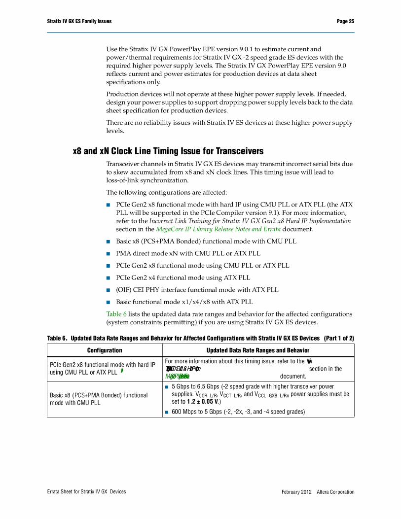
x8 and xN Clock Line Timing Issue for TransceiversTransceiver channels in Stratix IV GX ES devices may transmit incorrect serial bits due to skew accumulated from x8 and xN clock lines. This timing issue will lead to loss-of-link synchronization.
The following configurations are affected:
■ PCIe Gen2 x8 functional mode with hard IP using CMU PLL or ATX PLL (the ATX PLL will be supported in the PCIe Compiler version 9.1). For more information, refer to the Incorrect Link Training for Stratix IV GX Gen2 x8 Hard IP Implementation section in the MegaCore IP Library Release Notes and Errata document.
■ Basic x8 (PCS+PMA Bonded) functional mode with CMU PLL
■ PMA direct mode xN with CMU PLL or ATX PLL
■ PCIe Gen2 x8 functional mode using CMU PLL or ATX PLL
■ PCIe Gen2 x4 functional mode using ATX PLL
■ (OIF) CEI PHY interface functional mode with ATX PLL
■ Basic functional mode x1/x4/x8 with ATX PLL
Table 6 lists the updated data rate ranges and behavior for the affected configurations (system constraints permitting) if you are using Stratix IV GX ES devices.
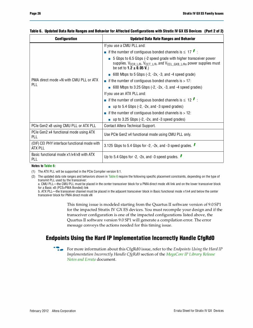
Table 6. Updated Data Rate Ranges and Behavior for Affected Configurations with Stratix IV GX ES Devices (Part 1 of 2)
Configuration Updated Data Rate Ranges and Behavior
PCIe Gen2 x8 functional mode with hard IP using CMU PLL or ATX PLL (1)
For more information about this timing issue, refer to the Incorrect Link Training for Stratix IV GX Gen2 x8 Hard IP Implementation section in the MegaCore IP Library Release Notes and Errata document.
Basic x8 (PCS+PMA Bonded) functional mode with CMU PLL
■ 5 Gbps to 6.5 Gbps (-2 speed grade with higher transceiver power supplies. VCCR_L/R, VCCT_L/R, and VCCL_GXB_L/Rn power supplies must be set to 1.2 ± 0.05 V.)
■ 600 Mbps to 5 Gbps (-2, -2x, -3, and -4 speed grades)
Page 26 Stratix IV GX ES Family Issues
February 2012 Altera Corporation Errata Sheet for Stratix IV GX Devices
This timing issue is modeled starting from the Quartus II software version of 9.0 SP1 for the impacted Stratix IV GX ES devices. You must recompile your design and if the transceiver configuration is one of the impacted configurations listed above, the Quartus II software version 9.0 SP1 will generate a compilation error. The error message conveys the actions needed for this timing issue.
Endpoints Using the Hard IP Implementation Incorrectly Handle CfgRd0
f For more information about this CfgRd0 issue, refer to the Endpoints Using the Hard IP Implementation Incorrectly Handle CfgRd0 section of the MegaCore IP Library Release Notes and Errata document.
PMA direct mode ×N with CMU PLL or ATX PLL
If you use a CMU PLL and:
■ if the number of contiguous bonded channels is ≤ 17 (2):
■ 5 Gbps to 6.5 Gbps (-2 speed grade with higher transceiver power supplies. VCCR_L/R, VCCT_L/R, and VCCL_GXB_L/Rn power supplies must be set to 1.2 ± 0.05 V.)
■ 600 Mbps to 5 Gbps (-2, -2x, -3, and -4 speed grade)
■ if the number of contiguous bonded channels is > 17:
■ 600 Mbps to 3.25 Gbps (-2, -2x, -3, and -4 speed grades)
If you use an ATX PLL and:
■ if the number of contiguous bonded channels is ≤ 12 (2):
■ up to 5.4 Gbps (-2, -2x, and -3 speed grades)
■ if the number of contiguous bonded channels is > 12:
■ up to 3.25 Gbps (-2, -2x, and -3 speed grades)
PCIe Gen2 x8 using CMU PLL or ATX PLL Contact Altera Technical Support.
PCIe Gen2 x4 functional mode using ATX PLL
Use PCIe Gen2 x4 functional mode using CMU PLL only.
(OIF) CEI PHY interface functional mode with ATX PLL
3.125 Gbps to 5.4 Gbps for -2, -2x, and -3 speed grades. (2)
Basic functional mode x1/x4/x8 with ATX PLL
Up to 5.4 Gbps for -2, -2x, and -3 speed grades. (2)
Notes to Table 6:
(1) The ATX PLL will be supported in the PCIe Compiler version 9.1.(2) The updated data rate ranges and behaviors shown in Table 6 require the following specific placement constraints, depending on the type of
transmit PLL used by the transceiver:a. CMU PLL—the CMU PLL must be placed in the center transceiver block for a PMA direct mode xN link and on the lower transceiver block for a Basic x8 (PCS+PMA Bonded) linkb. ATX PLL—the transceiver channel must be placed in the adjacent transceiver block in Basic functional mode x1/x4 and below the center transceiver block for PMA direct mode xN
Table 6. Updated Data Rate Ranges and Behavior for Affected Configurations with Stratix IV GX ES Devices (Part 2 of 2)
Configuration Updated Data Rate Ranges and Behavior

Stratix IV GX ES Family Issues Page 27
February 2012 Altera CorporationErrata Sheet for Stratix IV GX Devices
Higher VCC Power Supply LevelsStratix IV GX ES devices require higher VCC power supply levels (refer to Table 7).
EP4SGX230 ES devices require VCC, VCCD_PLL, and VCCHIP_L/R power supplies set to 0.95 V +/- 0.03 V for -2 and -2× speed grades only.
EP4SGX530 ES devices require VCC, VCCD_PLL, and VCCHIP_L/R power supplies set to 0.95 V +/- 0.03 V for all speed grades.
Use the PowerPlay EPE version 9.0.1 to estimate current and power/thermal requirements for Stratix IV GX ES devices with the required higher power supply levels. The PowerPlay EPE version 9.0 reflects current and power estimates for production devices at data sheet specifications only.
Production devices will not operate at these higher power supply levels. If needed, design your power supplies to support dropping power supply levels back to data sheet specification for production devices.
There are no reliability issues with Stratix IV GX ES devices at these higher power supply levels.
I/O JitterStratix IV GX ES devices may exhibit ± ~100 ps higher than expected jitter on all non-transceiver I/O pins. The actual amount of additional jitter is application and toggle-rate dependent. High-speed transceiver I/O pins are unaffected and perform to data sheet specifications.
Altera has fixed this I/O jitter issue in production devices, which meet all current jitter specifications.
If you are using Stratix IV GX ES devices, you need to account for this additional timing uncertainty in all non-transceiver I/O timing closure budgets.
Higher Minimum fINPFD SettingStratix IV GX ES devices may exhibit higher than expected PLL jitter at low fINPFD settings. Raising the minimum fINPFD to 25 MHz removes the additional PLL jitter in ES devices.
Altera has fixed this setting issue in production devices, which meet the current fINPFD minimum of 5 MHz.
Table 7. Power Supply Levels for Stratix IV GX ES Devices
Power Supply Power Supply Level (V) Description
VCC 0.95 Core voltage and periphery circuitry power supply
VCCD_PLL 0.95 PLL digital power supply
VCCHIP_L 0.95 Transceiver hardware interoperability platform digital power (left side)
VCCHIP_R 0.95 Transceiver hardware interoperability platform digital power (right side)

Page 28 Stratix IV GX ES Family Issues
February 2012 Altera Corporation Errata Sheet for Stratix IV GX Devices
If you are using Stratix IV GX ES devices, review your fINPFD settings by searching under “Nominal PFD Frequency” in each PLL section of your .fit.rpt compilation report file. If needed, recompile your design in the Quartus II software with modified PLL settings to achieve the higher minimum fINPFD.
f For more information about the ALTPLL megafunction, refer to the Quartus II Development Software Handbook or the Phase-Locked Loops (ALTPLL) Megafunction User Guide.
High I/O Pin Leakage CurrentTop and bottom I/O pin leakage current is higher for Stratix IV GX ES devices than production devices. Side I/O banks are not affected. For Stratix IV GX ES device I/O pin leakage current on top and bottom I/O banks, refer to Table 8.
These I/O pin leakage current values apply to Stratix IV GX ES silicon only and not to production silicon.
Higher Standby Current for VCC Power SupplyYou can expect to see higher standby ICC values on the VCC power supply for Stratix IV GX ES devices than indicated in the Quartus II software version 9.0 and the PowerPlay EPE version 9.0. The higher standby ICC current for the VCC power supply is fixed in production devices.
Use the PowerPlay EPE version 9.0.1 to estimate current and power/thermal requirements for the Stratix IV GX ES device. The PowerPlay EPE version 9.0 will not be updated with these higher standby current values.
Reduced M9K/M144K PerformanceM9K/M144K fMAX and tCO performance for Stratix IV GX ES devices may be lower than indicated in the Quartus II software version 8.1. Compile your design in the Quartus II software version 9.0 to estimate the impact on your design.
Table 8. I/O Pin Leakage Current for Top and Bottom I/O Banks
Temp.I/O Bank Voltage
Units3.0 V 2.5 V 1.8 V 1.5 V 1.2 V
25°C 35 25 15 11 9 μA
85°C 140 100 60 45 35 μA

Stratix IV GX ES Family Issues Page 29
February 2012 Altera CorporationErrata Sheet for Stratix IV GX Devices
Reduced Settings for TransceiversThere are reduced settings for the M counter of the ALTGX transmitter (TX) PLLs and receiver (RX) CDRs in the EP4SGX230 ES device transceiver blocks. Settings with M=16 and M=20 in all ALTGX PLLs are removed from Basic modes and all protocol configurations. These changes resulted in blocking one configuration for Sonet OC-48 (RefCLK = 77.76 MHz).
Update your design in the ALTGX MegaWizard Plug-In Manager in the Quartus II software version 9.0 and recompile the design. In some cases, you may have to change your ALTGX input reference frequency, which can be done using the available GPLL resources or external clock inputs.
DPA Misalignment Stratix IV GX DPA circuitry for ES devices occasionally become stuck at the initial configured phase or take significantly longer than expected to select the optimum phase. A non-ideal phase may result in data bit errors, even after the DPA lock signal has gone high. Resetting the DPA circuit may not alleviate the problem; in fact, resetting it might trigger the problem. LVDS receivers configured in DPA mode are affected. LVDS receivers configured in soft CDR mode with 0 parts-per-million (ppm) difference (synchronous interface) are also affected.
For applications with flexibility in the choice of training patterns, Altera recommends choosing bit sequences with more data transitions and a non-cyclical pattern similar to a PRBS or K28.5 code sequence.
For applications using a fixed, cyclical, or data transition sparse training pattern (for example, if you are using the SPI 4.2 protocol, which specifies a training pattern of ten 0s and ten 1s), turn on the DPA PLL Calibration option (available in the Quartus II software version 9.0) in the ALTLVDS MegaWizard Plug-In Manager.
1 There are two caveats when enabling the DPA PLL Calibration option:
■ PLL merging (merging RX and RX or merging RX and TX PLL) is not automatically supported by the ALTLVDS megafunction; use the external PLL option to handle PLL merging separately.
■ Timing for all PLL outputs is pulled in by 1/4 of the voltage controlled oscillator (VCO) phase during the PLL calibration process. This timing must be taken into account for external I/O pin timing interfaces and for clock domain transfers (without a FIFO) when the clocks are not all from this same PLL.
f For more information about the DPA PLL Calibration option, refer to the LVDS SERDES Transmitter/Receiver (ALTLVDS_TX and ALTLVDS_RX) Megafunction User Guide planned release corresponding to the Quartus II software version 9.0. Until the User Guide is updated, in the interim, file a service request using mySupport.

Page 30 Document Revision History
February 2012 Altera Corporation Errata Sheet for Stratix IV GX Devices
Document Revision HistoryTable 9 lists the revision history for this errata sheet.
Table 9. Document Revision History (Part 1 of 2)
Date Version Changes
February 2012 6.1 Changed Stratix V reference to Stratix IV in Table 1.
December 2011 6.0 Added the “PLL phasedone Signal Stuck at Low” section.
September 2011 5.9■ Added the “Remote System Upgrade” section.
■ Minor text edits.
June 2011 5.8 Added the “EDCRC False Errors” section.
March 2011 5.7 Updated the “I/O Jitter” section of Table 1.
December 2010 5.6 Added the “PCI Express (PCIe) Gen2 Protocol Link Establishment Issue” section.
October 2010 5.5■ Added the “Quartus II Software Incorrect Setting for Transceiver CDR in All Modes Except
PCIe Mode” and “Dynamic Reconfiguration Issue Between PCIe Mode and Any Other Transceiver Mode” sections.
September 2010 5.4
■ Added the “Quartus II Mapping Issue with PCIe Interfaces Using the Hard IP Block” section.
■ Added links to Table 3.
■ Added three headings with links to improve bookmark navigation.
May 2010 5.3 Added the “I/O Jitter” section.
April 2010 5.2
■ Added “Fast Passive Parallel Mode Configuration Failures at High DCLK Frequency”
■ Added “FPP Mode Configuration Failures When the Minimum Hold Time (tDH) is set to 0 ns or 24 ns”
■ Updated “DPA Misalignment” and removed this issue from Production devices section
■ Updated Table 2
■ Updated “Higher Power Supply Current During Power-Up for VCCPD and VCCA_L/R”
January 2010 5.1
■ Added “Transmitter PLL Lock (pll_locked) Status Signal”
■ Updated:
■ “Stratix IV GX Power-up Sequencing on Production Devices”
■ “×8 and ×N Clock Line Timing Issue for Transceivers”
■ Added “DPA Misalignment” section to production devices.
November 2009 5.0
Added:
■ “Stratix IV GX Production Devices”
■ “M144K RAM Block Lock-Up”
■ “×8 and ×N Clock Line Timing Issue for Transceivers”
■ “Stratix IV GX Power-up Issue on Production Devices”
Updated the following with link to software patch:
■ “M144K Write with Dual-Port Dual-Clock Modes”
■ “CRC Error Detection Feature”
Updated with fix in “Automatic Clock Switchover”.
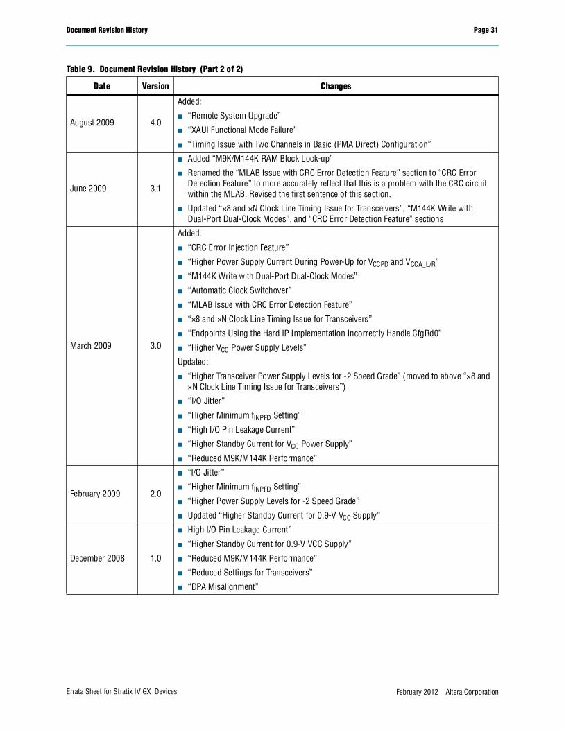
Document Revision History Page 31
February 2012 Altera CorporationErrata Sheet for Stratix IV GX Devices
August 2009 4.0
Added:
■ “Remote System Upgrade”
■ “XAUI Functional Mode Failure”
■ “Timing Issue with Two Channels in Basic (PMA Direct) Configuration”
June 2009 3.1
■ Added “M9K/M144K RAM Block Lock-up”
■ Renamed the “MLAB Issue with CRC Error Detection Feature” section to “CRC Error Detection Feature” to more accurately reflect that this is a problem with the CRC circuit within the MLAB. Revised the first sentence of this section.
■ Updated “×8 and ×N Clock Line Timing Issue for Transceivers”, “M144K Write with Dual-Port Dual-Clock Modes”, and “CRC Error Detection Feature” sections
March 2009 3.0
Added:
■ “CRC Error Injection Feature”
■ “Higher Power Supply Current During Power-Up for VCCPD and VCCA_L/R”
■ “M144K Write with Dual-Port Dual-Clock Modes”
■ “Automatic Clock Switchover”
■ “MLAB Issue with CRC Error Detection Feature”
■ “×8 and ×N Clock Line Timing Issue for Transceivers”
■ “Endpoints Using the Hard IP Implementation Incorrectly Handle CfgRd0”
■ “Higher VCC Power Supply Levels”
Updated:
■ “Higher Transceiver Power Supply Levels for -2 Speed Grade” (moved to above “×8 and ×N Clock Line Timing Issue for Transceivers”)
■ “I/O Jitter”
■ “Higher Minimum fINPFD Setting”
■ “High I/O Pin Leakage Current”
■ “Higher Standby Current for VCC Power Supply”
■ “Reduced M9K/M144K Performance”
February 2009 2.0
■ “I/O Jitter”
■ “Higher Minimum fINPFD Setting”
■ “Higher Power Supply Levels for -2 Speed Grade”
■ Updated “Higher Standby Current for 0.9-V VCC Supply”
December 2008 1.0
■ High I/O Pin Leakage Current”
■ “Higher Standby Current for 0.9-V VCC Supply”
■ “Reduced M9K/M144K Performance”
■ “Reduced Settings for Transceivers”
■ “DPA Misalignment”
Table 9. Document Revision History (Part 2 of 2)
Date Version Changes

Page 32 Document Revision History
February 2012 Altera Corporation Errata Sheet for Stratix IV GX Devices