Embed Size (px)
Citation preview

eGaN® FET DATASHEET
EPC – EFFICIENT POWER CONVERSION CORPORATION | WWW.EPC-CO.COM | COPYRIGHT 2013 | | PAGE 1
EPC2014
EPC2014 – Enhancement Mode Power Transistor
VDSS , 40 VRDS(ON) , 16 mWID , 10 A
Gallium Nitride is grown on Silicon Wafers and processed using standard CMOS equipment lever-aging the infrastructure that has been developed over the last 55 years. GaN’s exceptionally high electron mobility and low temperature coefficient allows very low RDS(ON), while its lateral device structure and majority carrier diode provide exceptionally low QG and zero QRR. The end result is a device that can handle tasks where very high switching frequency, and low on-time are beneficial as well as those where on-state losses dominate.
EPC2014 eGaN® FETs are supplied only inpassivated die form with solder bumps
Applications• HighSpeedDC-DCconversion• ClassDAudio• HardSwitchedandHighFrequencyCircuits
Benefits• UltraHighEfficiency• UltraLowRDS(on)
• UltralowQG
• Ultrasmallfootprint
EFFICIENT POWER CONVERSION
Maximum Ratings
VDSDrain-to-Source Voltage (up to 10,000 5ms pulses at 125° C) 48 V
Drain-to-Source Voltage (Continuous) 40 V
ID
Continuous (TA = 25˚C, θJA = 40) 10A
Pulsed (25˚C, Tpulse = 300 µs) 40
VGS
Gate-to-Source Voltage 6V
Gate-to-Source Voltage -5
TJ Operating Temperature -40 to 150˚C
TSTG Storage Temperature -40 to 150
PARAMETER TEST CONDITIONS MIN TYP MAX UNIT
Static Characteristics (TJ= 25˚C unless otherwise stated)
BVDSS Drain-to-Source Voltage VGS = 0 V, ID = 125 µA 40 V
IDSS Drain Source Leakage VDS = 32 V, VGS = 0 V 50 100 µA
IGSS
Gate-Source Forward Leakage VGS = 5 V 0.4 2mA
Gate-Source Reverse Leakage VGS = -5 V 0.1 0.5
VGS(TH) Gate Threshold Voltage VDS = VGS, ID = 2 mA 0.7 1.4 2.5 V
RDS(ON) Drain-Source On Resistance VGS = 5 V, ID = 5 A 12 16 mΩ
Source-Drain Characteristics (TJ= 25˚C unless otherwise stated)
VSD Source-Drain Forward VoltageIS = 0.5 A, VGS = 0 V, T = 25˚C 1.3
VIS = 0.5 A, VGS = 0 V, T = 125˚C 1.4
Thermal Characteristics
RθJC Thermal Resistance, Junction to Case 6.9 ˚C/W
RθJB Thermal Resistance, Junction to Board 32 ˚C/W
RθJA Thermal Resistance, Junction to Ambient (Note 1) 80 ˚C/W
TYP
Note 1: RθJA is determined with the device mounted on one square inch of copper pad, single layer 2 oz copper on FR4 board. See http://epc-co.com/epc/documents/product-training/Appnote_Thermal_Performance_of_eGaN_FETs.pdf for details.
All measurements were done with substrate shorted to source.
HAL
NEW PRODUCT
eGaN® FET DATASHEET
EPC – EFFICIENT POWER CONVERSION CORPORATION | WWW.EPC-CO.COM | COPYRIGHT 2013 | | PAGE 2
EPC2014I D
Drai
n Cu
rrent
(A)
VDS – Drain to Source Voltage (V)
40
35
30
25
20
15
10
5
00 0.2 0.4 0.6 0.8 1 1.2 1.4 1.6 1.8 2
I D Dr
ain
Curre
nt (A
)
VGS – Gate to Source Voltage (V)
40
25
30
35
20
15
10
5
00 0.5 1 1.5 2 2.5 3 3.5 4
25˚C125˚C
VDS = 3 V
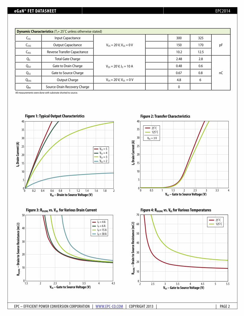
Figure 1: Typical Output Characteristics Figure 2: Transfer Characteristics
VGS = 5VGS = 4VGS = 3VGS = 2
R DS(
ON) –
Dra
in to
Sour
ce R
esist
ance
(mΩ
)
VGS – Gate to Source Voltage (V)
40
50
30
20
10
01.5 2 2.5 3 3.5 4 4.5
ID = 4 AID = 6 AID = 15 AID = 30 A
R DS(
ON) –
Dra
in to
Sour
ce R
esist
ance
(mΩ
)
VGS – Gate to Source Voltage (V)
60
70
50
40
30
20
10
02 2.5 3 3.5 4 4.5 5 5.5
25˚C125˚C
Figure 3: RDS(ON) vs. VGS for Various Drain Current Figure 4: RDS(ON) vs. VGS for Various Temperatures
All measurements were done with substrate shorted to source.
Dynamic Characteristics (TJ= 25˚C unless otherwise stated)
CISS Input Capacitance
VDS = 20 V, VGS = 0 V
300 325
170 pFCOSS Output Capacitance 150
CRSS Reverse Transfer Capacitance 10.2 12.5
QG Total Gate Charge
VDS = 20 V, ID = 10 A
2.48 2.8
nC
QGD Gate to Drain Charge 0.48 0.6
QGS Gate to Source Charge 0.67 0.8
QOSS Output Charge 4.8 6
QRR Source-Drain Recovery Charge 0
VDS = 20 V, V = 0 VGS
eGaN® FET DATASHEET
EPC – EFFICIENT POWER CONVERSION CORPORATION | WWW.EPC-CO.COM | COPYRIGHT 2013 | | PAGE 3
EPC2014I SD
– So
urce
to D
rain
Curre
nt (A
)
VSD – Source to Drain Voltage (V)
15
20
10
5
0 0
0.5 1 1.5 2 2.5 3 3.5
Norm
alize
d On-
Stat
e Res
istan
ce –
RDS
(ON)
T – Junction Temperature ( ˚C )
TJ – Junction Temperature ( ˚C )
2.2
2
1.8
1.6
1.4
1.2
1
0.8-20 0 20 40 60 80 100 120 140 160
ID = 10 AVGS = 5 V
I G –
Gate
Curre
nt (A
)
VGS – Gate-to-Source Voltage (V)
.03
.025
.02
.015
.01
.005
00 1 2 3 4 5 6
25˚C125˚C
Norm
alize
d Thr
esho
ld Vo
ltage 1.2
1.4
1.6
1
0.8
0.6
0.4
0.2-20 0 20 40 60 80 100 120 140 160
ID = 2 mA
Figure 7: Reverse Drain-Source Characteristics Figure 8: Normalized On Resistance vs. Temperature
Figure 10: Gate CurrentFigure 9: Normalized Threshold Voltage vs. Temperature
J
25˚C125˚C
VGS = 0 V
V GS –
Gat
e to S
ourc
e Vol
tage
(V)
C – Ca
pacit
ance
(nF)
VDS – Drain to Source Voltage (V)
0.35
0.3
0.25
0.2
0.15
0.1
0.05
00 5 10 15 20 25 30 35 40
COSS = CGD + CSD
CISS = CGD + CGS
CRSS = CGD
QG – Gate Charge (nC)
5
4
3
2
1
00 0.5 1 1.5 2 2.5
ID = 10 AVD = 20 V
Figure 5: Capacitance Figure 6: Gate Charge
All measurements were done with substrate shortened to source.
eGaN® FET DATASHEET
EPC – EFFICIENT POWER CONVERSION CORPORATION | WWW.EPC-CO.COM | COPYRIGHT 2013 | | PAGE 4
EPC2014
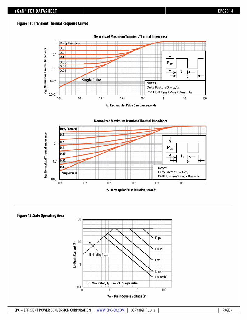
Figure 11: Transient Thermal Response Curves
Figure 12: Safe Operating Area
Duty Factors:
Notes:Duty Factor: D = t1/t2
Peak TJ = PDM x ZθJB x RθJB + TB
PDM
t1
t2
0.50.20.10.050.020.01
Single Pulse
1
0.1
0.01
0.001
0.000110-5 10-4 10-3 10-2 10-1 1 10 100
tp, Rectangular Pulse Duration, seconds
Normalized Maximum Transient Thermal Impedance
Z θJB
, Nor
mal
ized T
herm
al Im
peda
nce
Normalized Maximum Transient Thermal Impedance
tp, Rectangular Pulse Duration, seconds
Duty Factors:
Notes:Duty Factor: D = t1/t2
Peak TJ = PDM x ZθJC x RθJC + TC
PDM
t1
t2
0.5
0.2
0.1
0.05
0.02
0.01
Single Pulse
Z θJC
, Nor
mal
ized T
herm
al Im
peda
nce
10-510-6 10-4 10-3 10-2 10-1 1
1
0.1
0.01
0.001
0.1
1
10
100
0.1 1 10 100
I D- D
rain
Curre
nt (A
)
VDS - Drain-Source Voltage (V)
limited by RDS(ON)
TJ = Max Rated, TC = +25°C, Single Pulse
10 µs
100 µs
1 ms
10 ms100 ms/DC
eGaN® FET DATASHEET
EPC – EFFICIENT POWER CONVERSION CORPORATION | WWW.EPC-CO.COM | COPYRIGHT 2013 | | PAGE 5
EPC2014
DIE OUTLINESolder Bar View
Side View
B
A
X2e
f
g g
c
d X2 2
3 5
1
4
fX3
815 M
ax
100 +
/- 20
SEATING PLANE
(685
)
DIM MIN Nominal MAX
A 1672 1702 1732B 1057 1087 1117c 834 837 840d 327 330 333e 235 250 265f 195 200 205g 400 400 400
MICROMETERS
2014
YYYY
ZZZZ
Die orientation dot
Gate Pad bump is under this corner
Part Number
Laser Markings
Part #Marking Line 1
Lot_Date CodeMarking line 2
Lot_Date CodeMarking Line 3
EPC2014 2014 YYYY ZZZZ
DIE MARKINGS
TAPE AND REEL CONFIGURATION4mm pitch, 8mm wide tape on 7” reel
7” reel
a
d e f g
c
b
EPC2014 (note 1) Dimension (mm) target min max
a 8.00 7.90 8.30 b 1.75 1.65 1.85
c (see note) 3.50 3.45 3.55 d 4.00 3.90 4.10 e 4.00 3.90 4.10
f (see note) 2.00 1.95 2.05 g 1.5 1.5 1.6
Note 1: MSL 1 (moisture sensitivity level 1) classi�ed according to IPC/JEDEC industry standard.Note 2: Pocket position is relative to the sprocket hole measured as true position of the pocket, not the pocket hole.
Dieorientation
dot
Gatesolder bar is
under thiscorner
Die is placed into pocketsolder bar side down
(face side down)
Loaded Tape Feed Direction
eGaN® FET DATASHEET
EPC – EFFICIENT POWER CONVERSION CORPORATION | WWW.EPC-CO.COM | COPYRIGHT 2013 | | PAGE 6
EPC2014
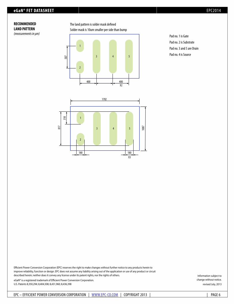
400 400 X2
507 1087
1702
X3 180 180
817
3101
3 5
2
4
1
3 5
2
4
400 400 X2
507 1087
1702
X3 180 180
817
3101
3 5
2
4
1
3 5
2
4
RECOMMENDEDLAND PATTERN (measurements in µm)
Information subject to change without notice.
revised July, 2013
Efficient Power Conversion Corporation (EPC) reserves the right to make changes without further notice to any products herein to improve reliability, function or design. EPC does not assume any liability arising out of the application or use of any product or circuit described herein; neither does it convey any license under its patent rights, nor the rights of others.
eGaN® is a registered trademark of Efficient Power Conversion Corporation.U.S. Patents 8,350,294; 8,404,508; 8,431,960; 8,436,398
Pad no. 1 is Gate
Pad no. 2 is Substrate
Pad no. 3 and 5 are Drain
Padno.4isSource
The land pattern is solder mask definedSolder mask is 10um smaller per side than bump


![BAB II TINJAUAN PUSTAKAeprints.umm.ac.id/35672/3/jiptummpp-gdl-arirobiuli-48901... · 2017-11-14 · 10 Gambar 2.6 Simbol Transistor MOSFET Mode Enhancement [9]. (a). N-Channel Enhancement](https://img.dokumen.tips/doc/110x75/5e9da1fd111da33d79475dc0/bab-ii-tinjauan-2017-11-14-10-gambar-26-simbol-transistor-mosfet-mode-enhancement.jpg)