Embed Size (px)
Citation preview
EM2420
Ember Part Number: 120-0049-000C EM2420 Datasheet Page 1 of 89
EM2420 2.4 GHz IEEE 802.15.4 / ZigBee RF Transceiver
Applications
• 2.4 GHz IEEE 802.15.4 systems • ZigBee systems • Consumer Electronics
• Industrial Control • Home/building automation • PC peripherals
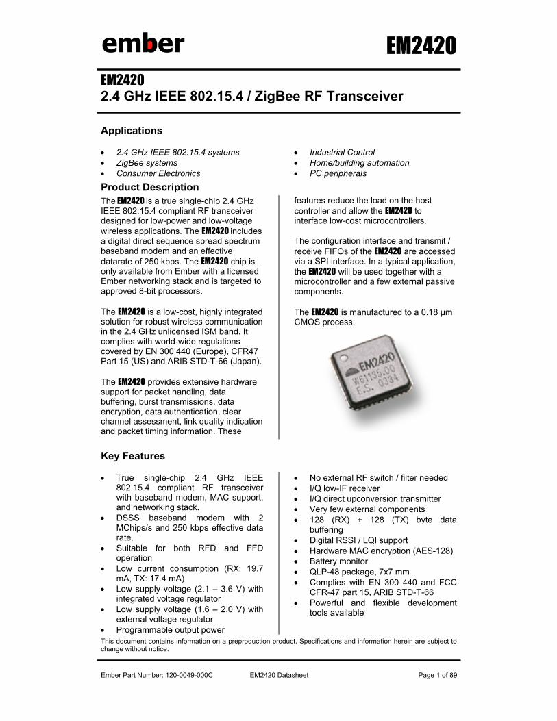
Product Description The EM2420 is a true single-chip 2.4 GHz IEEE 802.15.4 compliant RF transceiver designed for low-power and low-voltage wireless applications. The EM2420 includes a digital direct sequence spread spectrum baseband modem and an effective datarate of 250 kbps. The EM2420 chip is only available from Ember with a licensed Ember networking stack and is targeted to approved 8-bit processors.
The EM2420 is a low-cost, highly integrated solution for robust wireless communication in the 2.4 GHz unlicensed ISM band. It complies with world-wide regulations covered by EN 300 440 (Europe), CFR47 Part 15 (US) and ARIB STD-T-66 (Japan).
The EM2420 provides extensive hardware support for packet handling, data buffering, burst transmissions, data encryption, data authentication, clear channel assessment, link quality indication and packet timing information. These
features reduce the load on the host controller and allow the EM2420 to interface low-cost microcontrollers.
The configuration interface and transmit / receive FIFOs of the EM2420 are accessed via a SPI interface. In a typical application, the EM2420 will be used together with a microcontroller and a few external passive components.
The EM2420 is manufactured to a 0.18 µm CMOS process.
Key Features
• True single-chip 2.4 GHz IEEE 802.15.4 compliant RF transceiver with baseband modem, MAC support, and networking stack.
• DSSS baseband modem with 2 MChips/s and 250 kbps effective data rate.
• Suitable for both RFD and FFD operation
• Low current consumption (RX: 19.7 mA, TX: 17.4 mA)
• Low supply voltage (2.1 – 3.6 V) with integrated voltage regulator
• Low supply voltage (1.6 – 2.0 V) with external voltage regulator
• Programmable output power
• No external RF switch / filter needed • I/Q low-IF receiver • I/Q direct upconversion transmitter • Very few external components • 128 (RX) + 128 (TX) byte data
buffering • Digital RSSI / LQI support • Hardware MAC encryption (AES-128) • Battery monitor • QLP-48 package, 7x7 mm • Complies with EN 300 440 and FCC
CFR-47 part 15, ARIB STD-T-66 • Powerful and flexible development
tools available
This document contains information on a preproduction product. Specifications and information herein are subject to change without notice.
EM2420
Ember Part Number: 120-0049-000C EM2420 Datasheet Page 2 of 89
EM2420
Ember Part Number: 120-0049-000C EM2420 Datasheet Page 3 of 89
Table of contents
Abbreviations_____________________________________________________________________5 References _______________________________________________________________________6 Features _________________________________________________________________________7 Absolute Maximum Ratings_________________________________________________________8 Electrical Specifications ____________________________________________________________9 Pin Assignment __________________________________________________________________14 Circuit Description _______________________________________________________________16 Application Circuit _______________________________________________________________18
Input / output matching ___________________________________________________________18 Bias resistor ____________________________________________________________________18 Crystal ________________________________________________________________________18 Voltage regulator________________________________________________________________18 Power supply decoupling and filtering _______________________________________________18
IEEE 802.15.4 Modulation Format __________________________________________________22 Configuration Overview ___________________________________________________________23 Evaluation Software ______________________________________________________________24 4-wire Serial Configuration and Data Interface________________________________________25
Register access _________________________________________________________________25 Status byte _____________________________________________________________________26 Command strobes _______________________________________________________________27 RAM access____________________________________________________________________27 FIFO access ____________________________________________________________________29 Multiple SPI access ______________________________________________________________29
Microcontroller Interface and Pin Description ________________________________________30 Configuration interface ___________________________________________________________30 Receive mode __________________________________________________________________31 RXFIFO overflow _______________________________________________________________31 Transmit mode__________________________________________________________________32 General control and status pins _____________________________________________________32
Demodulator, Symbol Synchronizer and Data Decision _________________________________33 Frame Format ___________________________________________________________________33
Synchronization header ___________________________________________________________34 Length field ____________________________________________________________________35 MAC protocol data unit___________________________________________________________35 Frame check sequence____________________________________________________________35
RF Data Buffering________________________________________________________________37 Buffered transmit mode___________________________________________________________37 Buffered receive mode ___________________________________________________________38 Unbuffered, serial mode __________________________________________________________38
Address Recognition ______________________________________________________________39 Acknowledge Frames _____________________________________________________________40 Radio control state machine ________________________________________________________42 MAC Security Operations (Encryption and Authentication) _____________________________44
Keys__________________________________________________________________________44
EM2420
Ember Part Number: 120-0049-000C EM2420 Datasheet Page 4 of 89
Nonce / counter _________________________________________________________________44 Stand-alone encryption ___________________________________________________________45 In-line security operations _________________________________________________________45 CTR mode encryption / decryption __________________________________________________46 CBC-MAC_____________________________________________________________________46 CCM _________________________________________________________________________46 Timing ________________________________________________________________________47
Linear IF and AGC Settings________________________________________________________48 RSSI / Energy Detection ___________________________________________________________48 Link Quality Indication ___________________________________________________________49 Clear Channel Assessment _________________________________________________________50 Frequency and Channel Programming_______________________________________________51 VCO and PLL Self-Calibration _____________________________________________________51
VCO _________________________________________________________________________51 PLL self-calibration______________________________________________________________51
Output Power Programming _______________________________________________________52 Voltage Regulator ________________________________________________________________53 Battery Monitor__________________________________________________________________53 Crystal Oscillator ________________________________________________________________55 Input / Output Matching __________________________________________________________56 Transmitter Test Modes ___________________________________________________________56
Unmodulated carrier _____________________________________________________________56 Modulated spectrum _____________________________________________________________57
System Considerations and Guidelines _______________________________________________59 Frequency hopping and multi-channel systems_________________________________________59 Data burst transmissions __________________________________________________________59 Crystal accuracy and drift _________________________________________________________59 Communication robustness ________________________________________________________59 Communication security __________________________________________________________59 Low cost systems________________________________________________________________60 Battery operated systems__________________________________________________________60 BER / PER measurements _________________________________________________________60
PCB Layout Recommendations _____________________________________________________61 Antenna Considerations ___________________________________________________________61 Configuration Registers ___________________________________________________________63 Test Output Signals_______________________________________________________________84 Package Description (QLP 48) ______________________________________________________86
Package thermal properties ________________________________________________________86 Soldering information ____________________________________________________________87 Plastic tube specification __________________________________________________________87 Carrier tape and reel specification___________________________________________________87
Ordering Information _____________________________________________________________88 General Information ______________________________________________________________89
EM2420
Ember Part Number: 120-0049-000C EM2420 Datasheet Page 5 of 89
Abbreviations
ADC - Analog to Digital Converter AES - Advanced Encryption Standard AGC - Automatic Gain Control ARIB - Association of Radio Industries and Businesses BER - Bit Error Rate CBC-MAC - Cipher Block Chaining Message Authentication Code CCA - Clear Cannel Assessment CCM - Counter mode + CBC-MAC CFR - Code of Federal Regulations CTR - Counter mode (encryption) CW - Continuous Wave DAC - Digital to Analog Converter DSSS - Direct Sequence Spread Spectrum ESD - Electro Static Discharge ESR - Equivalent Series Resistance EVM - Error Vector Magnitude FCC - Federal Communications Commission FCF - Frame Control Field FIFO - First In First Out FFCTRL - FIFO and Frame Control HSSD - High Speed Serial Debug IEEE - Institute of Electrical and Electronics Engineers IF - Intermediate Frequency ISM - Industrial, Scientific and Medical ITU-T - International Telecommunication Union – Telecommunication Standardization Sector I/O - Input / Output I/Q - In-phase / Quadrature-phase kbps - kilo bits per second LNA - Low-Noise Amplifier LO - Local Oscillator LQI - Link Quality Indication LSB - Least Significant Bit / Byte MAC - Medium Access Control MFR - MAC Footer MHR - MAC Header MIC - Message Integrity Code MPDU - MAC Protocol Data Unit MSDU - MAC Service Data Unit NA - Not Available NC - No Connect O-QPSK - Offset - Quadrature Phase Shift Keying PA - Power Amplifier PCB - Printed Circuit Board PER - Packet Error Rate PHY - Physical Layer PHR - PHY Header PLL - Phase Locked Loop PSDU - PHY Service Data Unit QLP - Quad Leadless Package RAM - Random Access Memory RBW - Resolution Bandwidth RF - Radio Frequency RSSI - Receive Signal Strength Indicator RX - Receive
EM2420
Ember Part Number: 120-0049-000C EM2420 Datasheet Page 6 of 89
SHR - Synchronisation Header SPI - Serial Peripheral Interface TBD - To Be Decided / To Be Defined T/R - Transmit / Receive TX - Transmit VCO - Voltage Controlled Oscillator VGA - Variable Gain Amplifier
References
[1] IEEE std. 802.15.4/D18 - 2003: Wireless Medium Access Control (MAC) and Physical Layer (PHY) specifications for Low Rate Wireless Personal Area Networks (LR-WPANs)
http://www.ieee802.org/15/pub/TG4.html
[2] NIST FIPS Pub 197: Advanced Encryption Standard (AES), Federal Information Processing Standards Publication 197, US Department of Commerce/N.I.S.T., November 20014. Available from the NIST website.
http://csrc.nist.gov/publications/fips/fips197/fips-197.pdf
[3] R. Housley, D. Whiting, N. Ferguson, Counter with CBC-MAC (CCM), submitted to NIST, June 3, 2002. Available from the NIST website.
http://csrc.nist.gov/publications/fips/fips197/fips-197.pdf
EM2420
Ember Part Number: 120-0049-000C EM2420 Datasheet Page 7 of 89
Features
• 2400 – 2483.5 MHz RF Transceiver Direct Sequence Spread Spectrum
(DSSS) transceiver 250 kbps data rate, 2 MChip/s chip
rate O-QPSK with half sine pulse shaping
modulation Very low current consumption (RX:
19.7 mA, TX: 17.4 mA) High sensitivity (-94 dBm) High adjacent channel rejection (39
dB) High alternate channel rejection (46
dB) On-chip VCO, LNA and PA Low supply voltage (2.1 – 3.6 V) with
on-chip voltage regulator Programmable output power I/Q low-IF soft decision receiver I/Q direct up-conversion transmitter
• Separate transmit and receive FIFOs 128 byte transmit data FIFO 128 byte receive data FIFO
• Very few external components Only reference crystal and a
minimized number of passives No external filters needed
• Easy configuration interface 4-wire SPI interface Serial clock up to 10 MHz
• 802.15.4 MAC hardware support: Automatic preamble generator Synchronization word
insertion/detection CRC-16 computation and checking
over the MAC payload
Clear Channel Assessment Energy detection / digital RSSI Link Quality Indication Full automatic MAC security (CTR,
CBC-MAC, CCM)
• 802.15.4 MAC hardware security: Automated security operations within
the receive and transmit FIFOs. CTR mode encryption / decryption CBC-MAC authentication CCM encryption / decryption and
authentication Stand-alone AES encryption
• Development tools available Ember Evaluation Kit: A twelve-node
evaluation kit designed to allow users to characterize their application environment and familiarize themselves with Ember's Embedded RF solutions and Network Management software.
Ember Developer Kit: Everything developers need to create Ember Enabled applications. The Ember Developer Kit includes breakout hardware, Ember RF modules and the EmberNet Stack, a self-organizing, self-healing, flexible networking stack that accommodates mesh, star and hybrid network topologies. The EmberNet Stack is accessible though a straightforward and powerful API.
• Small size QLP-48 package, 7 x 7 mm • Complies with EN 300 440 and FCC
CFR47 part 15, ARIB STD-T-66
EM2420
Ember Part Number: 120-0049-000C EM2420 Datasheet Page 8 of 89
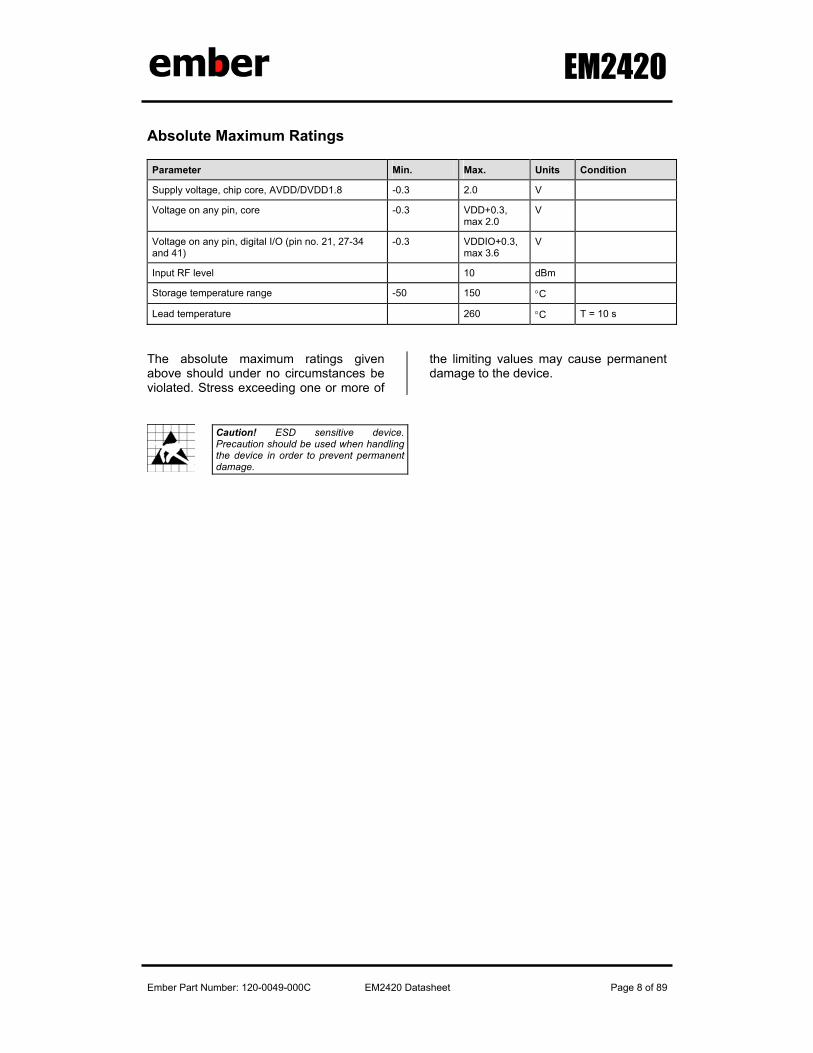
Absolute Maximum Ratings
Parameter Min. Max. Units Condition
Supply voltage, chip core, AVDD/DVDD1.8 -0.3 2.0 V
Voltage on any pin, core -0.3 VDD+0.3, max 2.0
V
Voltage on any pin, digital I/O (pin no. 21, 27-34 and 41)
-0.3 VDDIO+0.3, max 3.6
V
Input RF level 10 dBm
Storage temperature range -50 150 °C
Lead temperature 260 °C T = 10 s
The absolute maximum ratings given above should under no circumstances be violated. Stress exceeding one or more of
the limiting values may cause permanent damage to the device.
Caution! ESD sensitive device. Precaution should be used when handling the device in order to prevent permanent damage.
EM2420
Ember Part Number: 120-0049-000C EM2420 Datasheet Page 9 of 89
Electrical Specifications
Tc = 27°C, DVDD3.3 and VREG_IN = 3.0V, internal voltage regulator used if nothing else stated
Parameter Min. Typ. Max. Unit Condition / Note
Overall
Operating ambient temperature range
-40 85 °C
RF Frequency Range 2400 2483.5 MHz Programmable in 1 MHz steps, 5 MHz steps for compliance with [1]
Transmit Section
Transmit bit rate 250
250 kbps As defined by [1]
Transmit chip rate
2000 2000 kChips/s As defined by [1]
Nominal output power -3 0 dBm Delivered to a single ended 50 Ω load through a balun.
[1] requires minimum –3 dBm
Programmable output power range
40 dB
The output power is programmable in 8 steps from approximately –24 to 0 dBm.
Harmonics
2nd harmonic
3rd harmonic
-34
-60
dBc
dBc
At max output power delivered to a single ended 50 Ω load through a balun. See page 56.
Spurious emission
30 - 1000 MHz 1– 12.75 GHz 1.8 – 1.9 GHz 5.15 – 5.3 GHz
-36 -30 -47 -47
dBm dBm dBm dBm
Maximum output power.
Complies with EN 300 440, CFR47, Part 15 and ARIB STD-T-66
Error Vector Magnitude (EVM) 20 % Measured as defined by [1]
[1] requires max. 35 %
Optimum load impedance 115 + j180
Ω
Differential impedance as seen from the RF-port (RF_P and RF_N) towards the antenna. For matching details see the Input / Output Matching section on page 56.
EM2420
Ember Part Number: 120-0049-000C EM2420 Datasheet Page 10 of 89
Parameter Min. Typ. Max. Unit Condition / Note
Receive Section
Receiver Sensitivity
-90
-94
dBm
PER = 1%, as specified by [1]
Measured in 50 Ω single ended through a balun.
[1] requires –85 dBm
Saturation (maximum input level) 0 10 dBm PER = 1%, as specified by [1]
Measured in 50 Ω single ended through a balun.
[1] requires –20 dBm
Adjacent channel rejection
+ 5 MHz channel spacing
39
dB
Wanted signal @ -82 dBm, adjacent modulated channel at ± 5 MHz, PER = 1 %, as specified by [1].
[1] requires 0 dB
Adjacent channel rejection
- 5 MHz channel spacing
46
dB
Wanted signal @ -82 dBm, adjacent modulated channel at ± 5 MHz, PER = 1 %, as specified by [1].
[1] requires 0 dB
Alternate channel rejection
+ 10 MHz channel spacing
53
dB
Wanted signal @ -82 dBm, adjacent modulated channel at ± 10 MHz, PER = 1 %, as specified by [1]
[1] requires 30 dB
Alternate channel rejection
- 10 MHz channel spacing
57
dB
Wanted signal @ -82 dBm, adjacent modulated channel at ± 10 MHz, PER = 1 %, as specified by [1]
[1] requires 30 dB
Blocking / Desensitisation*
30 - 2000 MHz 2000 - 2399 MHz 2498 - 3000 MHz 3 – 12.75 GHz
(*Out-of-band spurious response rejection)
TBD TBD TBD TBD
dBm dBm dBm dBm
Wanted signal 3 dB above the sensitivity level, CW jammer, PER = 1%.
In-band spurious reception
TBD dB Ratio between sensitivity for an unwanted frequency to the sensitivity in the wanted channel. The signal source is a 802.15.4 modulated channel, swept over all channels from 2405 to 2480 MHz. Signal level for PER = 1%
Adjacent channels and image channel are excluded.
LO leakage -47 dBm
EM2420
Ember Part Number: 120-0049-000C EM2420 Datasheet Page 11 of 89
Parameter Min. Typ. Max. Unit Condition / Note
Spurious emission
30 – 1 GHz 1 – 12.75 GHz
-57 -47
dBm dBm
Complies with EN 300 440, CFR47, Part 15 and ARIB STD-T-66
Frequency error tolerance -300 300 kHz Difference between center frequency of the received RF signal and local oscillator frequency
[1] requires 200 kHz
Symbol rate error tolerance 120 ppm Difference between incoming symbol rate and the internally generated symbol rate
[1] requires 80 ppm
RSSI / Carrier Sense
Carrier sense level
-77 dBm Programmable in RSSI.CCA_THR
RSSI dynamic range
100 dB The range is approximately from –100 dBm to 0 dBm
RSSI accuracy ± 6
dB
See page 48 for details
RSSI linearity ± 3 dB
RSSI average time 128 µs 8 symbol periods, as specified by [1]
IF Section
Intermediate frequency (IF) 2 MHz
Frequency Synthesizer Section
Crystal oscillator frequency
16 MHz See page 55 for details.
Crystal frequency accuracy requirement
-40
40 ppm Including aging and temperature dependency, as specified by [1]
Crystal operation
Parallel
C4 and C5 are loading capacitors, see page 55
Crystal load capacitance
12 16 20 pF
16 pF recommended
Crystal ESR
60 Ω
Crystal oscillator start-up time 0.86 ms
16 pF load
EM2420
Ember Part Number: 120-0049-000C EM2420 Datasheet Page 12 of 89
Parameter Min. Typ. Max. Unit Condition / Note
Phase noise
-109 -117 -117 -117
dBc/Hz dBc/Hz dBc/Hz dBc/Hz
Unmodulated carrier
At ±1 MHz offset from carrier At ±2 MHz offset from carrier At ±3 MHz offset from carrier At ±5 MHz offset from carrier
PLL loop bandwidth 50 kHz
PLL lock time (RX / TX turnaround time)
192 µs
Digital Inputs/Outputs
Signal levels are referred to the voltage level at the pin DVDD3.3
Logic "0" input voltage
0 0.3* DVDD
V
Logic "1" input voltage
0.7* DVDD
DVDD V
Logic "0" output voltage 0
0.4 V Output current −8 mA, 3.3 V supply voltage
Logic "1" output voltage 2.5
VDD V Output current 8 mA, 3.3 V supply voltage
Logic "0" input current
NA -1 µA Input signal equals GND
Logic "1" input current
NA 1 µA Input signal equals VDD
FIFO setup time 20 ns TX un-buffered mode, minimum time FIFO must be ready before the positive edge of FIFOP
FIFO hold time
10 ns TX un-buffered mode, minimum time FIFO must be held after the positive edge of FIFOP
Serial interface pins (SCLK, SI, SO and CSn) timing specification
See Table 4 on page 26
Voltage Regulator
Input Voltage
2.1 3.0 3.6 V On the VREG_IN pin
Output Voltage
1.7 1.8 1.9 V On the VREG_OUT pin
Quiescent current
13 20 29 µA No current drawn from the VREG_OUT pin. Min and max numbers include 2.1 through 3.6 V input voltage
Start-up time
0.3 0.6 ms
EM2420
Ember Part Number: 120-0049-000C EM2420 Datasheet Page 13 of 89
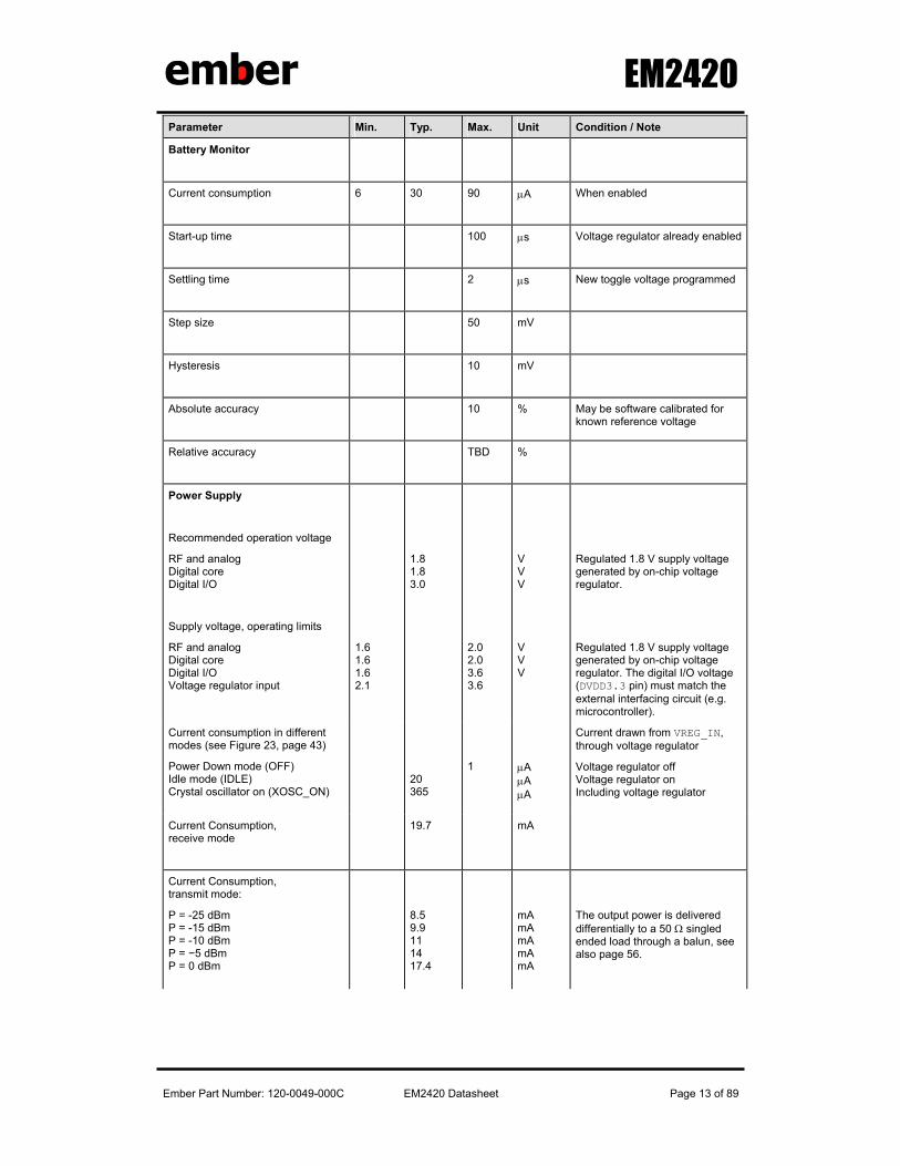
Parameter Min. Typ. Max. Unit Condition / Note
Battery Monitor
Current consumption
6 30 90 µA When enabled
Start-up time
100 µs Voltage regulator already enabled
Settling time
2 µs New toggle voltage programmed
Step size
50 mV
Hysteresis
10 mV
Absolute accuracy
10 % May be software calibrated for known reference voltage
Relative accuracy
TBD %
Power Supply
Recommended operation voltage
RF and analog Digital core Digital I/O
1.8 1.8 3.0
V V V
Regulated 1.8 V supply voltage generated by on-chip voltage regulator.
Supply voltage, operating limits
RF and analog Digital core Digital I/O Voltage regulator input
1.6 1.6 1.6 2.1
2.0 2.0 3.6 3.6
V V V
Regulated 1.8 V supply voltage generated by on-chip voltage regulator. The digital I/O voltage (DVDD3.3 pin) must match the external interfacing circuit (e.g. microcontroller).
Current consumption in different modes (see Figure 23, page 43)
Power Down mode (OFF) Idle mode (IDLE) Crystal oscillator on (XOSC_ON)
20 365
1
µA µA µA
Current drawn from VREG_IN, through voltage regulator
Voltage regulator off Voltage regulator on Including voltage regulator
Current Consumption, receive mode
19.7 mA
Current Consumption, transmit mode:
P = -25 dBm P = -15 dBm P = -10 dBm P = −5 dBm P = 0 dBm
8.5 9.9 11 14 17.4
mA mA mA mA mA
The output power is delivered differentially to a 50 Ω singled ended load through a balun, see also page 56.
EM2420
Ember Part Number: 120-0049-000C EM2420 Datasheet Page 14 of 89
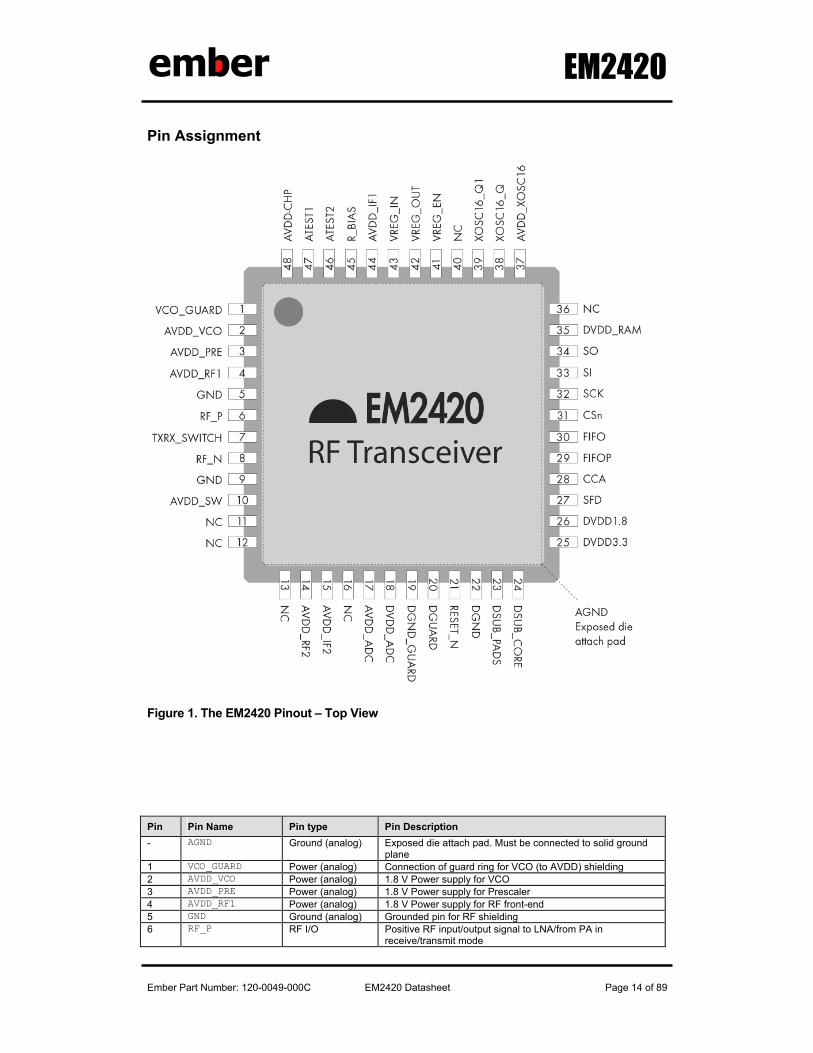
Pin Assignment
Figure 1. The EM2420 Pinout – Top View
Pin Pin Name Pin type Pin Description - AGND Ground (analog) Exposed die attach pad. Must be connected to solid ground
plane 1 VCO_GUARD Power (analog) Connection of guard ring for VCO (to AVDD) shielding 2 AVDD_VCO Power (analog) 1.8 V Power supply for VCO 3 AVDD_PRE Power (analog) 1.8 V Power supply for Prescaler 4 AVDD_RF1 Power (analog) 1.8 V Power supply for RF front-end 5 GND Ground (analog) Grounded pin for RF shielding 6 RF_P RF I/O Positive RF input/output signal to LNA/from PA in
receive/transmit mode
EM2420
Ember Part Number: 120-0049-000C EM2420 Datasheet Page 15 of 89
Pin Pin Name Pin type Pin Description 7 TXRX_SWITCH Power (analog) Common supply connection for integrated RF front-end. Must
be connected to RF_P and RF_N externally through a DC path
8 RF_N RF I/O Negative RF input/output signal to LNA/from PA in receive/transmit mode
9 GND Ground (analog) Grounded pin for RF shielding 10 AVDD_SW Power (analog) 1.8 V Power supply for LNA / PA switch 11 NC - No Connect 12 NC - No Connect 13 NC - No Connect 14 AVDD_RF2 Power (analog) 1.8 V Power supply for receive and transmit mixers 15 AVDD_IF2 Power (analog) 1.8 V Power supply for transmit / receive IF chain 16 NC - No Connect 17 AVDD_ADC Power (analog) 1.8 V Power supply for analog parts of ADCs and DACs 18 DVDD_ADC Power (digital) 1.8 V Power supply for digital parts of receive ADCs 19 DGND_GUARD Ground (digital) Ground connection for digital noise isolation 20 DGUARD Power (digital) 1.8 V Power supply connection for digital noise isolation 21 RESETn Digital Input Asynchronous, active low digital reset 22 DGND Ground (digital) Ground connection for digital core and pads 23 DSUB_PADS Ground (digital) Substrate connection for digital pads 24 DSUB_CORE Ground (digital) Substrate connection for digital modules 25 DVDD3.3 Power (digital) 3.3 V Power supply for digital I/Os 26 DVDD1.8 Power (digital) 1.8 V Power supply for digital core 27 SFD Digital output SFD (Start of Frame Delimiter) / digital mux output 28 CCA Digital output CCA (Clear Channel Assessment) / digital mux output 29 FIFOP Digital output High when number of bytes in FIFO exceeds threshold /
serial RF clock output in test mode 30 FIFO Digital I/O High when data in FIFO /
serial RF data input / output in test mode 31 CSn Digital input SPI Chip select, active low 32 SCLK Digital input SPI Clock input, up to 10 MHz 33 SI Digital input SPI Slave Input. Sampled on the positive edge of SCLK 34 SO Digital output
(tristate / pullup) SPI Slave Output. Updated on the negative edge of SCLK. Tristate when CSn high. Programmable internal pullup
35 DVDD_RAM Power (digital) 1.8 V Power supply for digital RAM 36 NC - No Connect 37 AVDD_XOSC16 Power (analog) 1.8 V crystal oscillator power supply 38 XOSC16_Q2 Analog I/O 16 MHz Crystal oscillator pin 2 39 XOSC16_Q1 Analog I/O 16 MHz Crystal oscillator pin 1 or external clock input 40 NC - No Connect 41 VREG_EN Digital input Voltage regulator enable, active high, held at VREG_IN
voltage level when active 42 VREG_OUT Power output Voltage regulator 1.8 V power supply output 43 VREG_IN Power (analog) Voltage regulator 2.1 to 3.6 V power supply input 44 AVDD_IF1 Power (analog) 1.8 V Power supply for transmit / receive IF chain 45 R_BIAS Analog output External precision resistor, 43 kΩ, ± 1 % 46 ATEST2 Analog I/O Analog test I/O for prototype and production testing 47 ATEST1 Analog I/O Analog test I/O for prototype and production testing 48 AVDD_CHP Power (analog) 1.8 V Power supply for phase detector and charge pump
NOTES:
The exposed die attach pad must be connected to solid ground plane as this is the main ground connection for the chip.
Note that digital inputs SCLK, SI and CSn are high-impedance inputs (no internal pull-up) and should have external pull-ups if not driven. SO is high-impedance when CSn is high. External pull-up should be used at SO to prevent floating input at microcontroller or the internal SO-pin pull-up should be enabled.
EM2420
Ember Part Number: 120-0049-000C EM2420 Datasheet Page 16 of 89
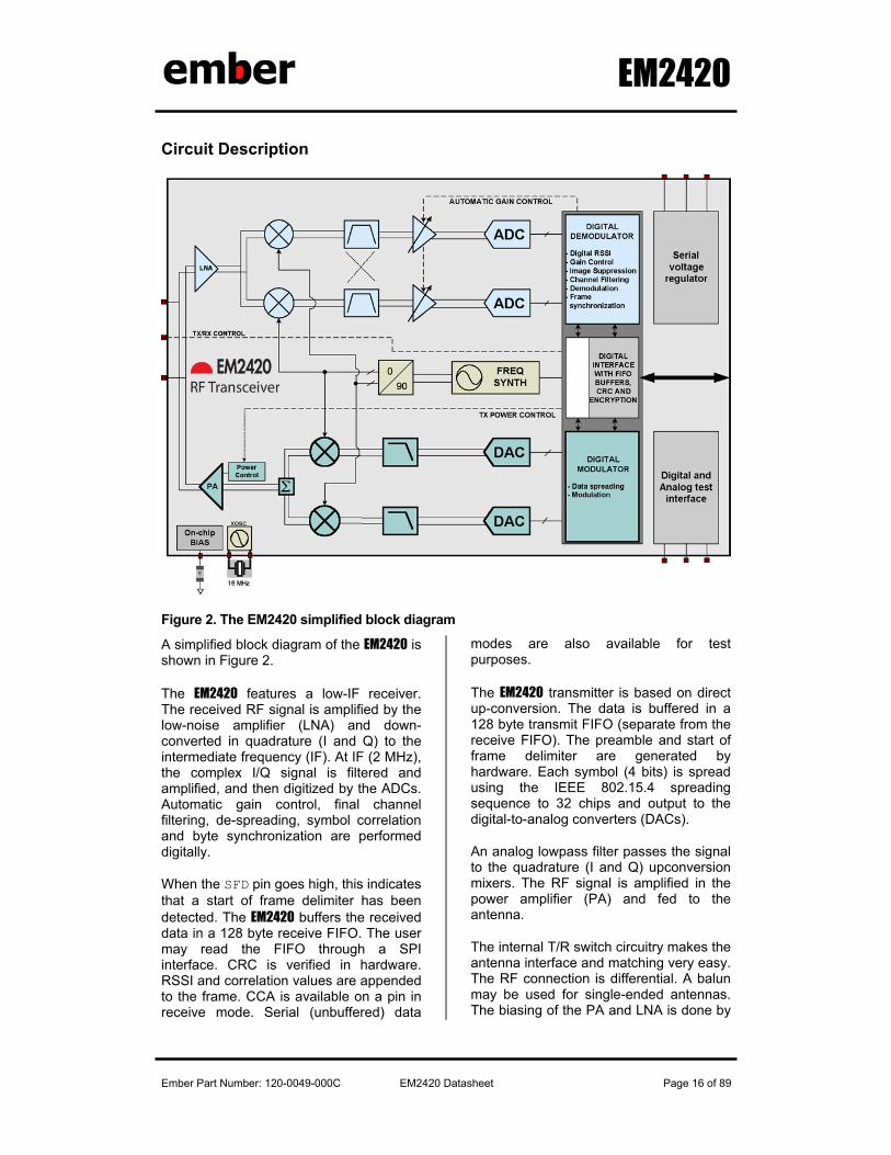
Circuit Description
Figure 2. The EM2420 simplified block diagram
A simplified block diagram of the EM2420 is shown in Figure 2.
The EM2420 features a low-IF receiver. The received RF signal is amplified by the low-noise amplifier (LNA) and down-converted in quadrature (I and Q) to the intermediate frequency (IF). At IF (2 MHz), the complex I/Q signal is filtered and amplified, and then digitized by the ADCs. Automatic gain control, final channel filtering, de-spreading, symbol correlation and byte synchronization are performed digitally.
When the SFD pin goes high, this indicates that a start of frame delimiter has been detected. The EM2420 buffers the received data in a 128 byte receive FIFO. The user may read the FIFO through a SPI interface. CRC is verified in hardware. RSSI and correlation values are appended to the frame. CCA is available on a pin in receive mode. Serial (unbuffered) data
modes are also available for test purposes.
The EM2420 transmitter is based on direct up-conversion. The data is buffered in a 128 byte transmit FIFO (separate from the receive FIFO). The preamble and start of frame delimiter are generated by hardware. Each symbol (4 bits) is spread using the IEEE 802.15.4 spreading sequence to 32 chips and output to the digital-to-analog converters (DACs).
An analog lowpass filter passes the signal to the quadrature (I and Q) upconversion mixers. The RF signal is amplified in the power amplifier (PA) and fed to the antenna.
The internal T/R switch circuitry makes the antenna interface and matching very easy. The RF connection is differential. A balun may be used for single-ended antennas. The biasing of the PA and LNA is done by

EM2420
Ember Part Number: 120-0049-000C EM2420 Datasheet Page 17 of 89
connecting RXTX_SWITCH to RF_P and RF_N through an external DC path.
The frequency synthesizer includes a completely on-chip LC VCO and a 90 degrees phase splitter for generating the I and Q LO signals to the down-conversion mixers in receive mode and up-conversion mixers in transmit mode. The VCO operates in the frequency range 4800 – 4966 MHz, and the frequency is divided by two when split in I and Q.
A crystal must be connected to XOSC16_Q1 and XOSC16_Q2 and provides the reference frequency for the synthesizer. A digital lock signal is available from the PLL.
The digital baseband includes support for frame handling, address recognition, data buffering and MAC security.
The 4-wire SPI serial interface is used for configuration and data buffering.
An on-chip voltage regulator delivers the regulated 1.8 V supply voltage. The voltage regulator may be enabled / disabled through a separate pin.
A battery monitor may optionally be used to monitor the unregulated power supply voltage. The battery monitor is configurable through the SPI interface.
EM2420
Ember Part Number: 120-0049-000C EM2420 Datasheet Page 18 of 89
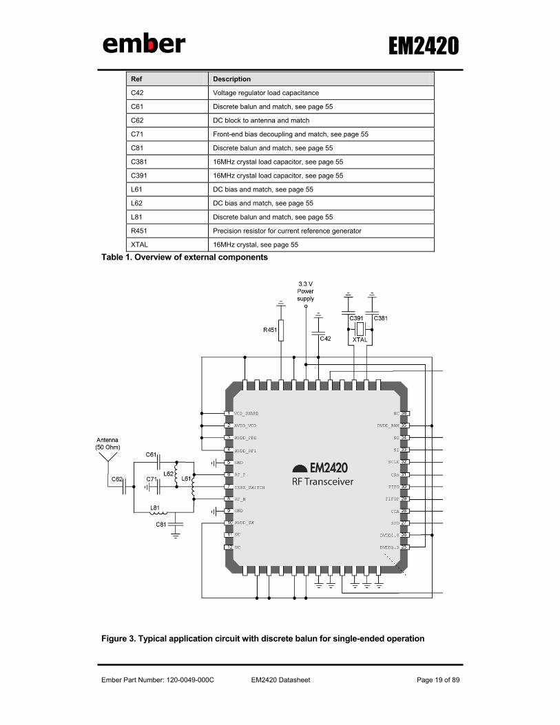
Application Circuit
Few external components are required for the operation of the EM2420. A typical application circuit is shown in Figure 3. The external components are described in Table 1 and typical values are given in Table 2.
Input / output matching
The RF input/output is high impedance and differential. The optimum differential load for the RF port is 115+j180 Ω.
When using an unbalanced antenna such as a monopole, a balun should be used in order to optimize performance. The balun can be implemented using low-cost discrete inductors and capacitors. The balun consists of C61, C62, C71, C81, L61, L62 and L72, and will match the RF input/output to 50 Ω, see Figure 3. L61 and L62 also provide DC biasing of the LNA/PA input/output. An internal T/R switch circuit is used to switch between the LNA and the PA. See Input/output matching section on page 55 for more details.
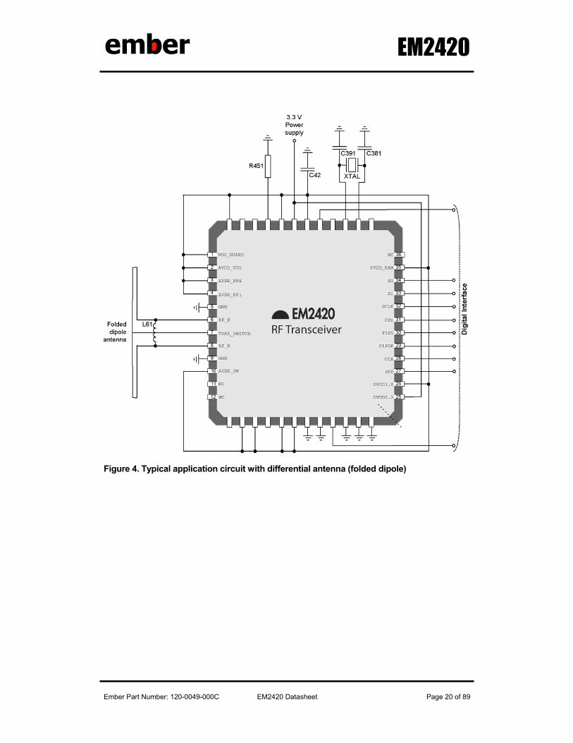
If a balanced antenna such as a folded dipole is used, the balun can be omitted. If the antenna also provides a DC path from TXRX_SWITCH pin to the RF pins, inductors are not needed for DC bias.
Figure 4 shows a typical application circuit with differential antenna. The dipole has a virtual ground point, hence bias is
provided without degradation in antenna performance.
A 27 nH series inductor may be connected to the TXRX_SWITCH pin to improve the transmitted EVM, but is not necessary to comply with the requirements in [1].
Bias resistor
The bias resistor R451 is used to set an accurate bias current.
Crystal
An external crystal with two loading capacitors (C381 and C391) is used for the crystal oscillator. See page 55 for details.
Voltage regulator
The on chip voltage regulator supplies all 1.8 V power supply inputs. C42 is required for stability of the regulator. A series resistor may be used to comply with the ESR requirement.
Power supply decoupling and filtering
Proper power supply decoupling must be used for optimum performance. The placement and size of the decoupling capacitors and the power supply filtering are very important to achieve the best performance in an application. Ember provides a compact reference design that should be followed very closely.
EM2420
Ember Part Number: 120-0049-000C EM2420 Datasheet Page 19 of 89
Ref Description
C42 Voltage regulator load capacitance
C61 Discrete balun and match, see page 55
C62 DC block to antenna and match
C71 Front-end bias decoupling and match, see page 55
C81 Discrete balun and match, see page 55
C381 16MHz crystal load capacitor, see page 55
C391 16MHz crystal load capacitor, see page 55
L61 DC bias and match, see page 55
L62 DC bias and match, see page 55
L81 Discrete balun and match, see page 55
R451 Precision resistor for current reference generator
XTAL 16MHz crystal, see page 55
Table 1. Overview of external components
Figure 3. Typical application circuit with discrete balun for single-ended operation
EM2420
Ember Part Number: 120-0049-000C EM2420 Datasheet Page 20 of 89
Figure 4. Typical application circuit with differential antenna (folded dipole)
EM2420
Ember Part Number: 120-0049-000C EM2420 Datasheet Page 21 of 89
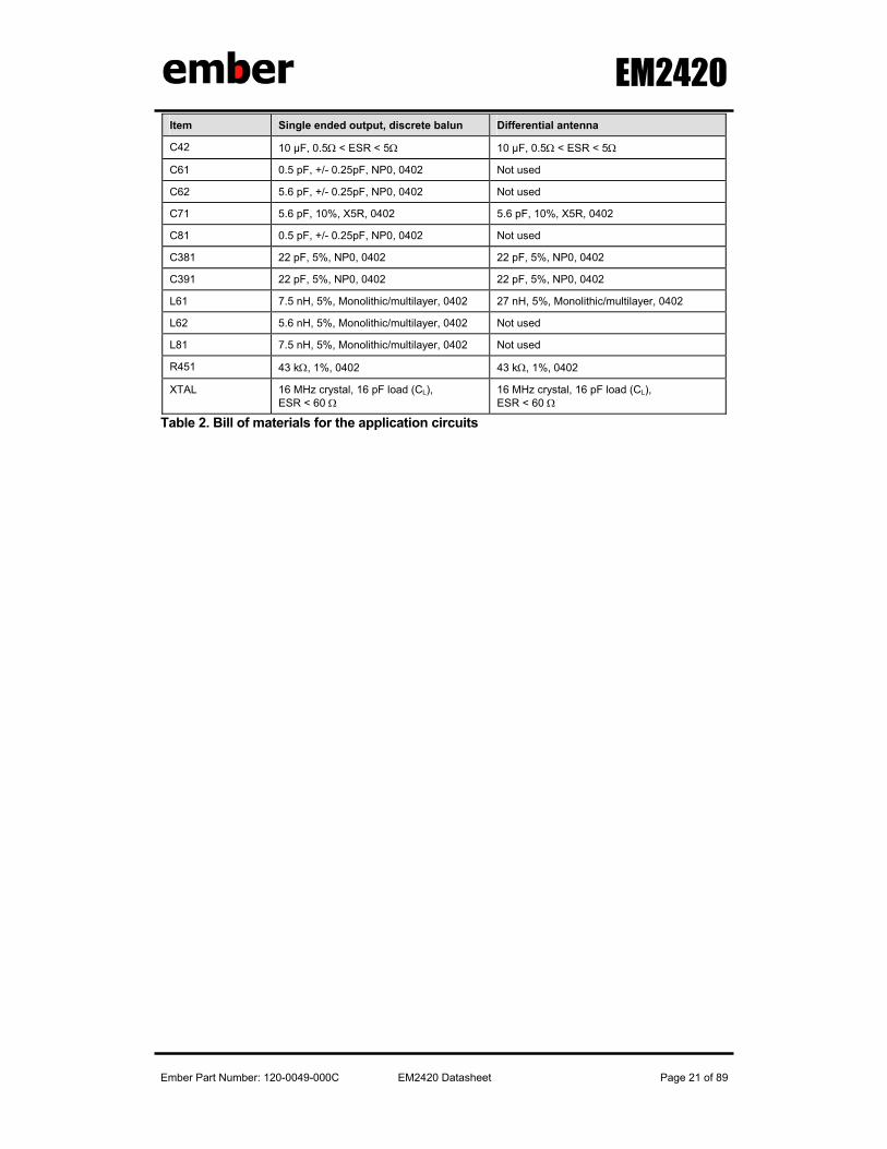
Item Single ended output, discrete balun Differential antenna
C42 10 µF, 0.5Ω < ESR < 5Ω 10 µF, 0.5Ω < ESR < 5Ω
C61 0.5 pF, +/- 0.25pF, NP0, 0402 Not used
C62 5.6 pF, +/- 0.25pF, NP0, 0402 Not used
C71 5.6 pF, 10%, X5R, 0402 5.6 pF, 10%, X5R, 0402
C81 0.5 pF, +/- 0.25pF, NP0, 0402 Not used
C381 22 pF, 5%, NP0, 0402 22 pF, 5%, NP0, 0402
C391 22 pF, 5%, NP0, 0402 22 pF, 5%, NP0, 0402
L61 7.5 nH, 5%, Monolithic/multilayer, 0402 27 nH, 5%, Monolithic/multilayer, 0402
L62 5.6 nH, 5%, Monolithic/multilayer, 0402 Not used
L81 7.5 nH, 5%, Monolithic/multilayer, 0402 Not used
R451 43 kΩ, 1%, 0402 43 kΩ, 1%, 0402
XTAL 16 MHz crystal, 16 pF load (CL), ESR < 60 Ω
16 MHz crystal, 16 pF load (CL), ESR < 60 Ω
Table 2. Bill of materials for the application circuits
EM2420
Ember Part Number: 120-0049-000C EM2420 Datasheet Page 22 of 89
IEEE 802.15.4 Modulation Format
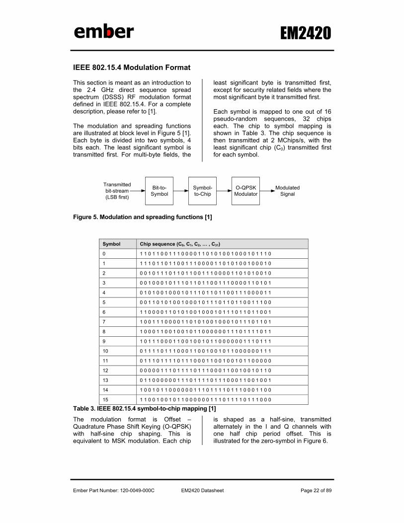
This section is meant as an introduction to the 2.4 GHz direct sequence spread spectrum (DSSS) RF modulation format defined in IEEE 802.15.4. For a complete description, please refer to [1].
The modulation and spreading functions are illustrated at block level in Figure 5 [1]. Each byte is divided into two symbols, 4 bits each. The least significant symbol is transmitted first. For multi-byte fields, the
least significant byte is transmitted first, except for security related fields where the most significant byte it transmitted first.
Each symbol is mapped to one out of 16 pseudo-random sequences, 32 chips each. The chip to symbol mapping is shown in Table 3. The chip sequence is then transmitted at 2 MChips/s, with the least significant chip (C0) transmitted first for each symbol.
Bit-to-Symbol
Symbol-to-Chip
O-QPSKModulator
Transmittedbit-stream(LSB first)
ModulatedSignal
Figure 5. Modulation and spreading functions [1]
Symbol Chip sequence (C0, C1, C2, … , C31)
0 1 1 0 1 1 0 0 1 1 1 0 0 0 0 1 1 0 1 0 1 0 0 1 0 0 0 1 0 1 1 1 0
1 1 1 1 0 1 1 0 1 1 0 0 1 1 1 0 0 0 0 1 1 0 1 0 1 0 0 1 0 0 0 1 0
2 0 0 1 0 1 1 1 0 1 1 0 1 1 0 0 1 1 1 0 0 0 0 1 1 0 1 0 1 0 0 1 0
3 0 0 1 0 0 0 1 0 1 1 1 0 1 1 0 1 1 0 0 1 1 1 0 0 0 0 1 1 0 1 0 1
4 0 1 0 1 0 0 1 0 0 0 1 0 1 1 1 0 1 1 0 1 1 0 0 1 1 1 0 0 0 0 1 1
5 0 0 1 1 0 1 0 1 0 0 1 0 0 0 1 0 1 1 1 0 1 1 0 1 1 0 0 1 1 1 0 0
6 1 1 0 0 0 0 1 1 0 1 0 1 0 0 1 0 0 0 1 0 1 1 1 0 1 1 0 1 1 0 0 1
7 1 0 0 1 1 1 0 0 0 0 1 1 0 1 0 1 0 0 1 0 0 0 1 0 1 1 1 0 1 1 0 1
8 1 0 0 0 1 1 0 0 1 0 0 1 0 1 1 0 0 0 0 0 0 1 1 1 0 1 1 1 1 0 1 1
9 1 0 1 1 1 0 0 0 1 1 0 0 1 0 0 1 0 1 1 0 0 0 0 0 0 1 1 1 0 1 1 1
10 0 1 1 1 1 0 1 1 1 0 0 0 1 1 0 0 1 0 0 1 0 1 1 0 0 0 0 0 0 1 1 1
11 0 1 1 1 0 1 1 1 1 0 1 1 1 0 0 0 1 1 0 0 1 0 0 1 0 1 1 0 0 0 0 0
12 0 0 0 0 0 1 1 1 0 1 1 1 1 0 1 1 1 0 0 0 1 1 0 0 1 0 0 1 0 1 1 0
13 0 1 1 0 0 0 0 0 0 1 1 1 0 1 1 1 1 0 1 1 1 0 0 0 1 1 0 0 1 0 0 1
14 1 0 0 1 0 1 1 0 0 0 0 0 0 1 1 1 0 1 1 1 1 0 1 1 1 0 0 0 1 1 0 0
15 1 1 0 0 1 0 0 1 0 1 1 0 0 0 0 0 0 1 1 1 0 1 1 1 1 0 1 1 1 0 0 0
Table 3. IEEE 802.15.4 symbol-to-chip mapping [1]
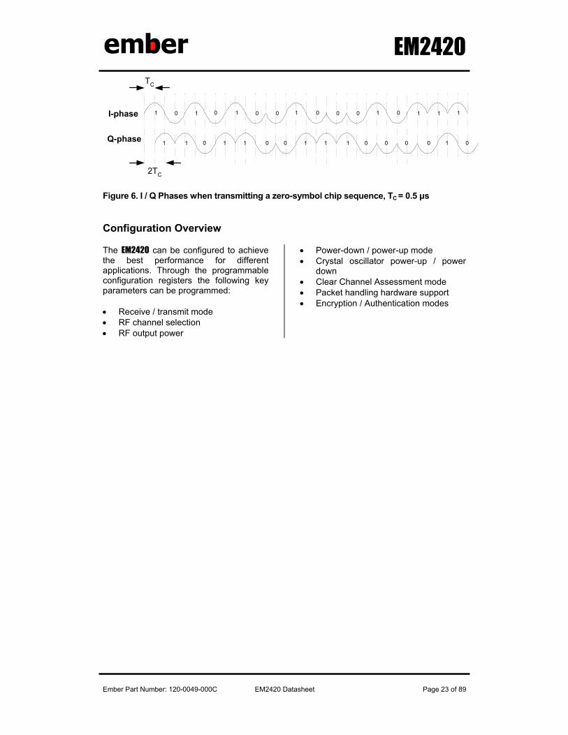
The modulation format is Offset – Quadrature Phase Shift Keying (O-QPSK) with half-sine chip shaping. This is equivalent to MSK modulation. Each chip
is shaped as a half-sine, transmitted alternately in the I and Q channels with one half chip period offset. This is illustrated for the zero-symbol in Figure 6.
EM2420
Ember Part Number: 120-0049-000C EM2420 Datasheet Page 23 of 89
1 0 1 0
1 1 0 1
I-phase
Q-phase
1 0 0 1
1 0 0 1
0 0 0
1 1 0 0
1 0 1 1
0 0 1 0
1
TC
2TC
Figure 6. I / Q Phases when transmitting a zero-symbol chip sequence, TC = 0.5 µs
Configuration Overview
The EM2420 can be configured to achieve the best performance for different applications. Through the programmable configuration registers the following key parameters can be programmed:
• Receive / transmit mode • RF channel selection • RF output power
• Power-down / power-up mode • Crystal oscillator power-up / power
down • Clear Channel Assessment mode • Packet handling hardware support • Encryption / Authentication modes
EM2420
Ember Part Number: 120-0049-000C EM2420 Datasheet Page 24 of 89
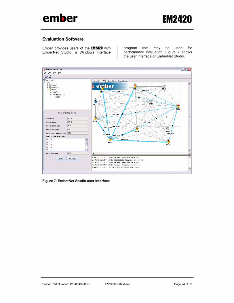
Evaluation Software
Ember provides users of the EM2420 with EmberNet Studio, a Windows interface
program that may be used for performance evaluation. Figure 7 shows the user interface of EmberNet Studio.
Figure 7. EmberNet Studio user interface
EM2420
Ember Part Number: 120-0049-000C EM2420 Datasheet Page 25 of 89
4-wire Serial Configuration and Data Interface
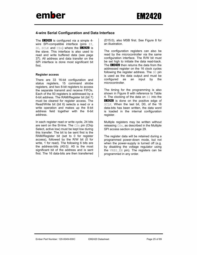
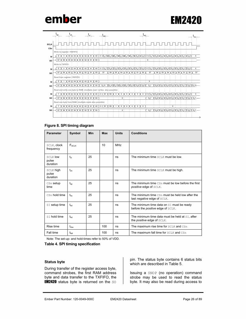
The EM2420 is configured via a simple 4-wire SPI-compatible interface (pins SI, SO, SCLK and CSn) where the EM2420 is the slave. This interface is also used to read and write buffered data (see page 37). All address and data transfer on the SPI interface is done most significant bit first.
Register access
There are 33 16-bit configuration and status registers, 15 command strobe registers, and two 8-bit registers to access the separate transmit and receive FIFOs. Each of the 50 registers is addressed by a 6-bit address. The RAM/Register bit (bit 7) must be cleared for register access. The Read/Write bit (bit 6) selects a read or a write operation and makes up the 8-bit address field together with the 6-bit address.
In each register read or write cycle, 24 bits are sent on the SI-line. The CSn pin (Chip Select, active low) must be kept low during this transfer. The bit to be sent first is the RAM/Register bit (set to 0 for register access), followed by the R/W bit (0 for write, 1 for read). The following 6 bits are the address-bits (A5:0). A5 is the most significant bit of the address and is sent first. The 16 data-bits are then transferred
(D15:0), also MSB first. See Figure 8 for an illustration.
The configuration registers can also be read by the microcontroller via the same configuration interface. The R/W bit must be set high to initiate the data read-back. The EM2420 then returns the data from the addressed register on the 16 clock cycles following the register address. The SO pin is used as the data output and must be configured as an input by the microcontroller.
The timing for the programming is also shown in Figure 8 with reference to Table 4. The clocking of the data on SI into the EM2420 is done on the positive edge of SCLK. When the last bit, D0, of the 16 data-bits has been written, the data word is loaded in the internal configuration register.
Multiple registers may be written without releasing CSn, as described in the Multiple SPI access section on page 29.
The register data will be retained during a programmed power-down mode, but not when the power-supply is turned off (e.g. by disabling the voltage regulator using the VREG_EN pin). The registers can be programmed in any order.
EM2420
Ember Part Number: 120-0049-000C EM2420 Datasheet Page 26 of 89
0 0 A5 A4 A3 A2 A0A1 DW15 DW14 DW13 DW12 DW11 DW10 DW9 DW8 DW7 DW6 DW5 DW4 DW3 DW2 DW1 DW0
S7 S6 S5 S4 S3 S2 S0S1
0 1 A5 A4 A3 A2 A0A1
DR15 DR14 DR13 DR12 DR11 DR10 DR9 DR8 DR7 DR6 DR5 DR4 DR3 DR2 DR1 DR0S7 S6 S5 S4 S3 S2 S0S1
Read from register / RXFIFO:
Write to register / RXFIFO:
X
X
X X X
DR15
SCLK
CSn
SI
SO
SI
SO
tsp tch tsdthd tns
tcl
1 A6 A5 A4 A3 A2 A0A1 B1 B0 0 X X X X X DW7 DW6 DW5 DW4 DW3 DW2 DW1 DW0
S7 S6 S5 S4 S3 S2 S0S1
1 A6 A5 A4 A3 A2 A0A1
DR7 DR6 DR5 DR4 DR3 DR2 DR1 DR0S7 S6 S5 S4 S3 S2 S0S1
Read one byte from RAM: (multiple reads also possible)
Read and write one byte to RAM: (multiple read / writes also possible)
X
X
X X X
DR7
B1 B0 1 X X X X XX
X
SI
SO
SI
SO
DR7 DR6 DR5 DR4 DR3 DR2 DR1 DR0 DR7
0 0 A5 A4 A3 A2 A0A1 DW7 DW6 DW5 DW4 DW3 DW2 DW1 DW0 DW7 DW6 DW5 DW4 DW3 DW2 DW1 DW0
S7 S6 S5 S4 S3 S2 S0S1
Write to TXFIFO:
X X XSI
SO S7 S6 S5 S4 S3 S2 S0S1 S7 S6 S5 S4 S3 S2 S0S1 S7
Figure 8. SPI timing diagram
Parameter Symbol
Min Max Units Conditions
SCLK, clock frequency
FSCLK
10 MHz
SCLK low pulse duration
tcl 25 ns The minimum time SCLK must be low.
SCLK high pulse duration
tch 25 ns The minimum time SCLK must be high.
CSn setup time
tsp
25 ns The minimum time CSn must be low before the first positive edge of SCLK.
CSn hold time tns 25 ns The minimum time CSn must be held low after the last negative edge of SCLK.
SI setup time tsd
25 ns The minimum time data on SI must be ready before the positive edge of SCLK.
SI hold time thd 25 ns The minimum time data must be held at SI, after the positive edge of SCLK.
Rise time trise 100 ns The maximum rise time for SCLK and CSn
Fall time tfall 100 ns The maximum fall time for SCLK and CSn
Note: The set-up- and hold-times refer to 50% of VDD.
Table 4. SPI timing specification
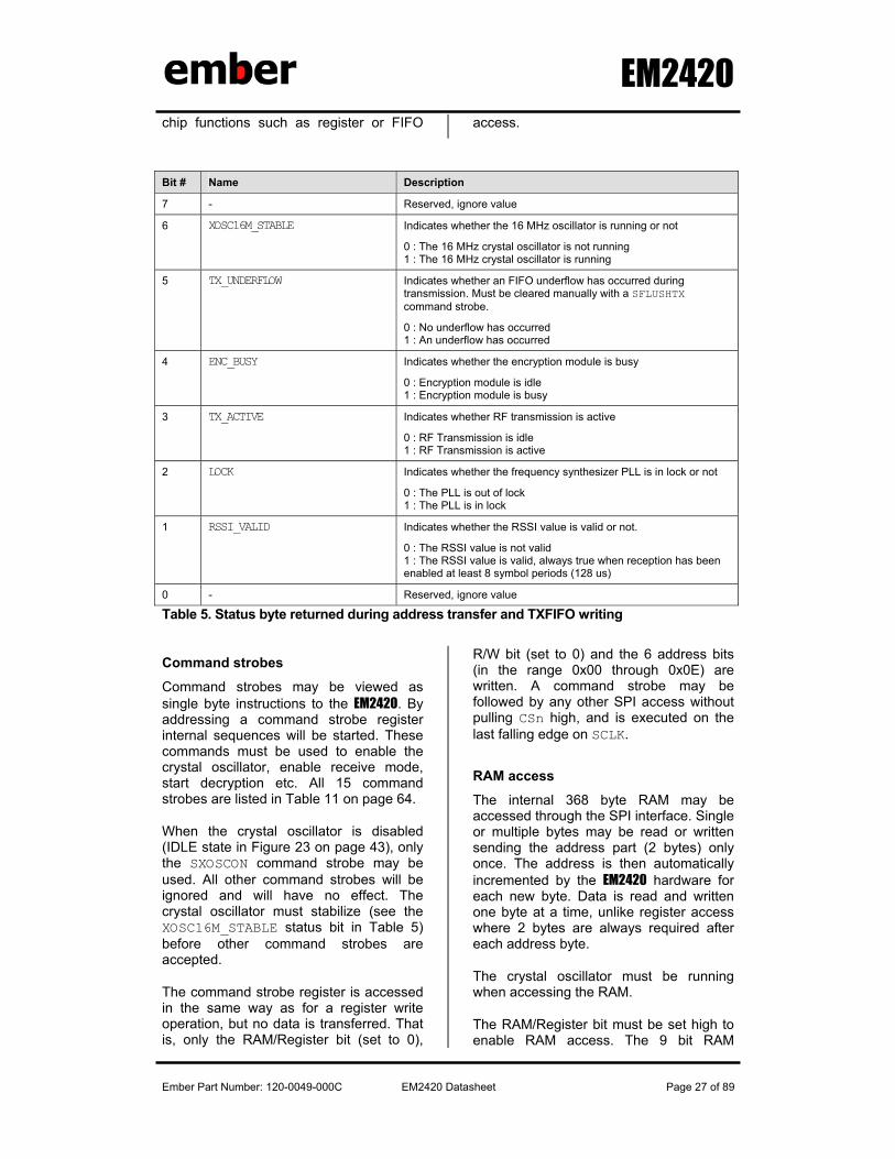
Status byte
During transfer of the register access byte, command strobes, the first RAM address byte and data transfer to the TXFIFO, the EM2420 status byte is returned on the SO
pin. The status byte contains 6 status bits which are described in Table 5.
Issuing a SNOP (no operation) command strobe may be used to read the status byte. It may also be read during access to
EM2420
Ember Part Number: 120-0049-000C EM2420 Datasheet Page 27 of 89
chip functions such as register or FIFO access.
Bit # Name Description
7 - Reserved, ignore value
6 XOSC16M_STABLE Indicates whether the 16 MHz oscillator is running or not
0 : The 16 MHz crystal oscillator is not running 1 : The 16 MHz crystal oscillator is running
5 TX_UNDERFLOW Indicates whether an FIFO underflow has occurred during transmission. Must be cleared manually with a SFLUSHTX command strobe.
0 : No underflow has occurred 1 : An underflow has occurred
4 ENC_BUSY Indicates whether the encryption module is busy
0 : Encryption module is idle 1 : Encryption module is busy
3 TX_ACTIVE Indicates whether RF transmission is active
0 : RF Transmission is idle 1 : RF Transmission is active
2 LOCK Indicates whether the frequency synthesizer PLL is in lock or not
0 : The PLL is out of lock 1 : The PLL is in lock
1 RSSI_VALID Indicates whether the RSSI value is valid or not.
0 : The RSSI value is not valid 1 : The RSSI value is valid, always true when reception has been enabled at least 8 symbol periods (128 us)
0 - Reserved, ignore value
Table 5. Status byte returned during address transfer and TXFIFO writing
Command strobes
Command strobes may be viewed as single byte instructions to the EM2420. By addressing a command strobe register internal sequences will be started. These commands must be used to enable the crystal oscillator, enable receive mode, start decryption etc. All 15 command strobes are listed in Table 11 on page 64.
When the crystal oscillator is disabled (IDLE state in Figure 23 on page 43), only the SXOSCON command strobe may be used. All other command strobes will be ignored and will have no effect. The crystal oscillator must stabilize (see the XOSC16M_STABLE status bit in Table 5) before other command strobes are accepted.
The command strobe register is accessed in the same way as for a register write operation, but no data is transferred. That is, only the RAM/Register bit (set to 0),
R/W bit (set to 0) and the 6 address bits (in the range 0x00 through 0x0E) are written. A command strobe may be followed by any other SPI access without pulling CSn high, and is executed on the last falling edge on SCLK.
RAM access
The internal 368 byte RAM may be accessed through the SPI interface. Single or multiple bytes may be read or written sending the address part (2 bytes) only once. The address is then automatically incremented by the EM2420 hardware for each new byte. Data is read and written one byte at a time, unlike register access where 2 bytes are always required after each address byte.
The crystal oscillator must be running when accessing the RAM.
The RAM/Register bit must be set high to enable RAM access. The 9 bit RAM
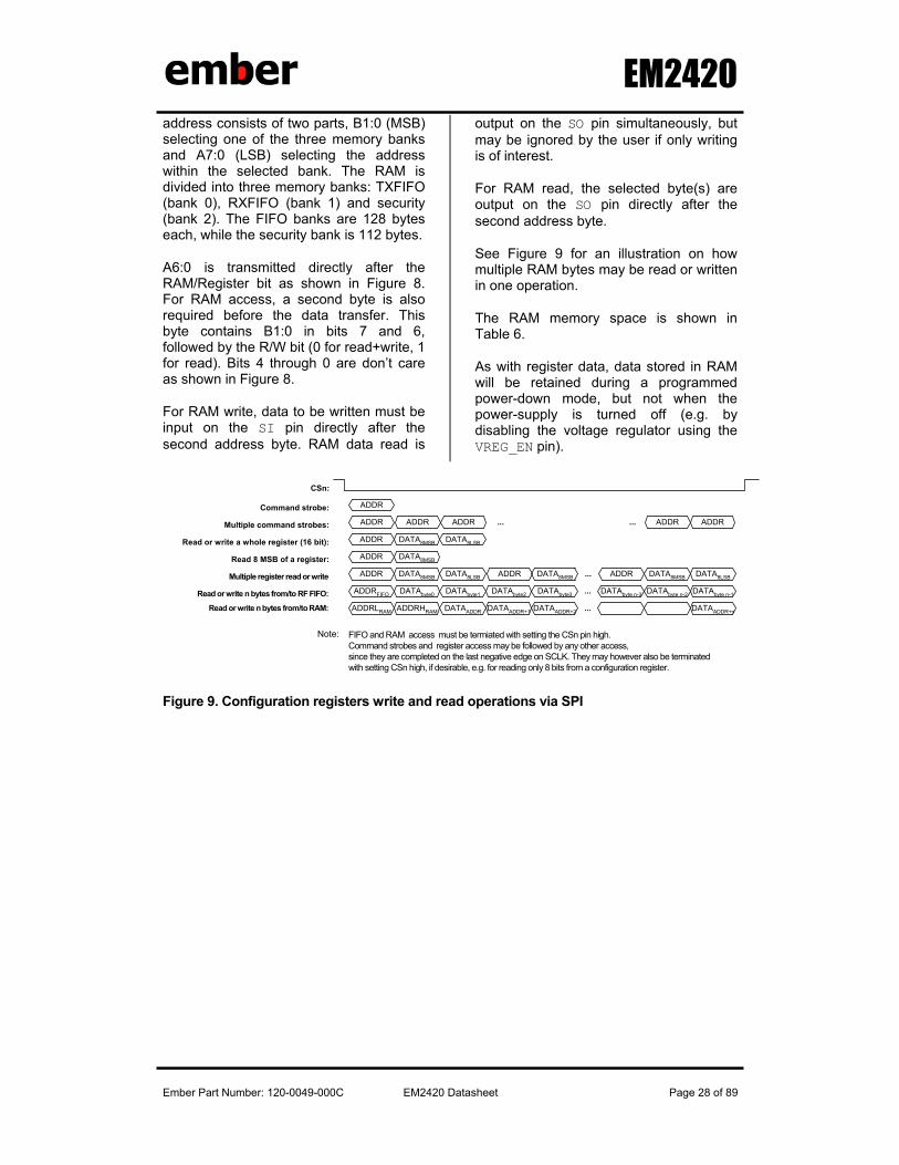
EM2420
Ember Part Number: 120-0049-000C EM2420 Datasheet Page 28 of 89
address consists of two parts, B1:0 (MSB) selecting one of the three memory banks and A7:0 (LSB) selecting the address within the selected bank. The RAM is divided into three memory banks: TXFIFO (bank 0), RXFIFO (bank 1) and security (bank 2). The FIFO banks are 128 bytes each, while the security bank is 112 bytes.
A6:0 is transmitted directly after the RAM/Register bit as shown in Figure 8. For RAM access, a second byte is also required before the data transfer. This byte contains B1:0 in bits 7 and 6, followed by the R/W bit (0 for read+write, 1 for read). Bits 4 through 0 are don’t care as shown in Figure 8.
For RAM write, data to be written must be input on the SI pin directly after the second address byte. RAM data read is
output on the SO pin simultaneously, but may be ignored by the user if only writing is of interest.
For RAM read, the selected byte(s) are output on the SO pin directly after the second address byte.
See Figure 9 for an illustration on how multiple RAM bytes may be read or written in one operation.
The RAM memory space is shown in Table 6.
As with register data, data stored in RAM will be retained during a programmed power-down mode, but not when the power-supply is turned off (e.g. by disabling the voltage regulator using the VREG_EN pin).
ADDR
CSn:
Command strobe:
Read or write a whole register (16 bit): DATA8MSBADDR DATA8LSB
Read 8 MSB of a register: DATA8MSBADDR
Multiple register read or write DATA8MSBADDR DATA8LSB DATA8MSB DATA8LSB...
Read or write n bytes from/to RF FIFO: DATAbyte0ADDRFIFO DATAbyte1 DATAbyte2 DATAbyte3 DATAbyte n-2 DATAbyte n-1...
ADDRMultiple command strobes: ADDR ADDR ... ADDR
ADDR DATA8MSB ADDR
DATAbyte n-3
ADDR...
Read or write n bytes from/to RAM: ADDRHRAMADDRLRAM DATAADDR DATAADDR+1 DATAADDR+2 DATAADDR+n...
FIFO and RAM access must be termiated with setting the CSn pin high.Command strobes and register access may be followed by any other access,since they are completed on the last negative edge on SCLK. They may however also be terminatedwith setting CSn high, if desirable, e.g. for reading only 8 bits from a configuration register.
Note:
Figure 9. Configuration registers write and read operations via SPI
EM2420
Ember Part Number: 120-0049-000C EM2420 Datasheet Page 29 of 89
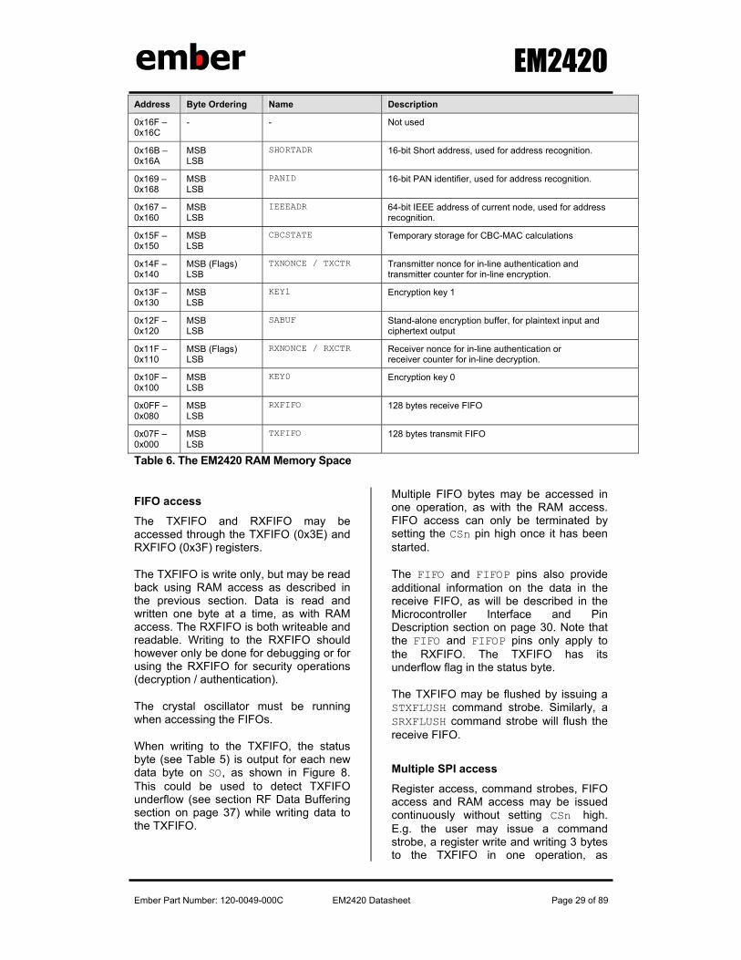
Address Byte Ordering Name Description
0x16F – 0x16C
- - Not used
0x16B – 0x16A
MSB LSB
SHORTADR 16-bit Short address, used for address recognition.
0x169 – 0x168
MSB LSB
PANID 16-bit PAN identifier, used for address recognition.
0x167 – 0x160
MSB LSB
IEEEADR 64-bit IEEE address of current node, used for address recognition.
0x15F – 0x150
MSB LSB
CBCSTATE Temporary storage for CBC-MAC calculations
0x14F – 0x140
MSB (Flags) LSB
TXNONCE / TXCTR Transmitter nonce for in-line authentication and transmitter counter for in-line encryption.
0x13F – 0x130
MSB LSB
KEY1 Encryption key 1
0x12F – 0x120
MSB LSB
SABUF Stand-alone encryption buffer, for plaintext input and ciphertext output
0x11F – 0x110
MSB (Flags) LSB
RXNONCE / RXCTR Receiver nonce for in-line authentication or receiver counter for in-line decryption.
0x10F – 0x100
MSB LSB
KEY0 Encryption key 0
0x0FF – 0x080
MSB LSB
RXFIFO 128 bytes receive FIFO
0x07F – 0x000
MSB LSB
TXFIFO 128 bytes transmit FIFO
Table 6. The EM2420 RAM Memory Space
FIFO access
The TXFIFO and RXFIFO may be accessed through the TXFIFO (0x3E) and RXFIFO (0x3F) registers.
The TXFIFO is write only, but may be read back using RAM access as described in the previous section. Data is read and written one byte at a time, as with RAM access. The RXFIFO is both writeable and readable. Writing to the RXFIFO should however only be done for debugging or for using the RXFIFO for security operations (decryption / authentication).
The crystal oscillator must be running when accessing the FIFOs.
When writing to the TXFIFO, the status byte (see Table 5) is output for each new data byte on SO, as shown in Figure 8. This could be used to detect TXFIFO underflow (see section RF Data Buffering section on page 37) while writing data to the TXFIFO.
Multiple FIFO bytes may be accessed in one operation, as with the RAM access. FIFO access can only be terminated by setting the CSn pin high once it has been started.
The FIFO and FIFOP pins also provide additional information on the data in the receive FIFO, as will be described in the Microcontroller Interface and Pin Description section on page 30. Note that the FIFO and FIFOP pins only apply to the RXFIFO. The TXFIFO has its underflow flag in the status byte.
The TXFIFO may be flushed by issuing a STXFLUSH command strobe. Similarly, a SRXFLUSH command strobe will flush the receive FIFO.
Multiple SPI access
Register access, command strobes, FIFO access and RAM access may be issued continuously without setting CSn high. E.g. the user may issue a command strobe, a register write and writing 3 bytes to the TXFIFO in one operation, as
EM2420
Ember Part Number: 120-0049-000C EM2420 Datasheet Page 30 of 89
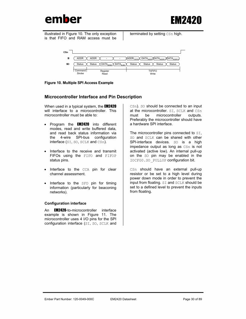
illustrated in Figure 10. The only exception is that FIFO and RAM access must be
terminated by setting CSn high.
CSn
SI ADDRADDR
DATA8MSB DATA8LSB
DATAADDR+1
SO
ADDRTXFIFO DATAADDR DATAADDR+2
StatusStatus
- -
StatusStatus Status Status
CommandStrobe
RegisterRead
TXFIFOWrite
Figure 10. Multiple SPI Access Example
Microcontroller Interface and Pin Description
When used in a typical system, the EM2420 will interface to a microcontroller. This microcontroller must be able to:
• Program the EM2420 into different modes, read and write buffered data, and read back status information via the 4-wire SPI-bus configuration interface (SI, SO, SCLK and CSn).
• Interface to the receive and transmit FIFOs using the FIFO and FIFOP status pins.
• Interface to the CCA pin for clear channel assessment.
• Interface to the SFD pin for timing information (particularly for beaconing networks).
Configuration interface
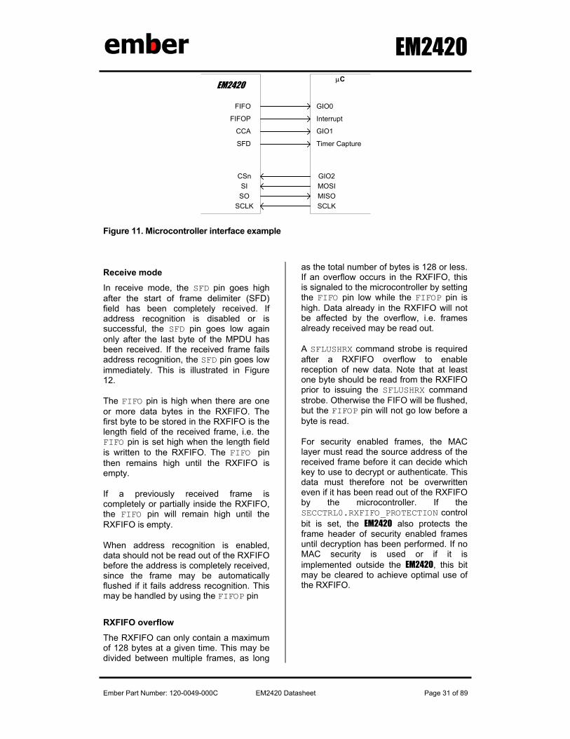
An EM2420-to-microcontroller interface example is shown in Figure 11. The microcontroller uses 4 I/O pins for the SPI configuration interface (SI, SO, SCLK and
CSn). SO should be connected to an input at the microcontroller. SI, SCLK and CSn must be microcontroller outputs. Preferably the microcontroller should have a hardware SPI interface.
The microcontroller pins connected to SI, SO and SCLK can be shared with other SPI-interface devices. SO is a high impedance output as long as CSn is not activated (active low). An internal pull-up on the SO pin may be enabled in the IOCFG0.SO_PULLUP configuration bit.
CSn should have an external pull-up resistor or be set to a high level during power down mode in order to prevent the input from floating. SI and SCLK should be set to a defined level to prevent the inputs from floating.
EM2420
Ember Part Number: 120-0049-000C EM2420 Datasheet Page 31 of 89
EM2420µC
CSnSISO
SCLK
MOSIMISOSCLK
GIO2
FIFO
FIFOP
CCA
SFD
GIO0
Interrupt
GIO1
Timer Capture
Figure 11. Microcontroller interface example
Receive mode
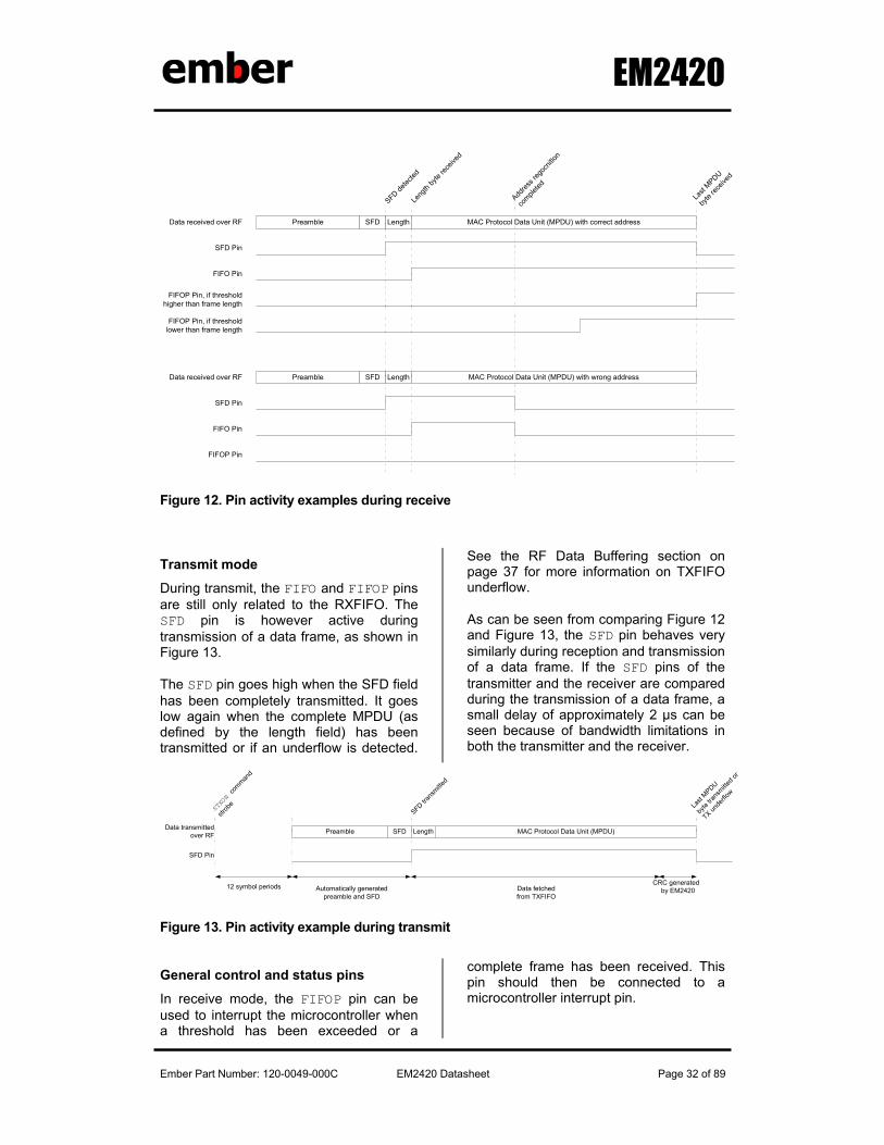
In receive mode, the SFD pin goes high after the start of frame delimiter (SFD) field has been completely received. If address recognition is disabled or is successful, the SFD pin goes low again only after the last byte of the MPDU has been received. If the received frame fails address recognition, the SFD pin goes low immediately. This is illustrated in Figure 12.
The FIFO pin is high when there are one or more data bytes in the RXFIFO. The first byte to be stored in the RXFIFO is the length field of the received frame, i.e. the FIFO pin is set high when the length field is written to the RXFIFO. The FIFO pin then remains high until the RXFIFO is empty.
If a previously received frame is completely or partially inside the RXFIFO, the FIFO pin will remain high until the RXFIFO is empty.
When address recognition is enabled, data should not be read out of the RXFIFO before the address is completely received, since the frame may be automatically flushed if it fails address recognition. This may be handled by using the FIFOP pin
RXFIFO overflow
The RXFIFO can only contain a maximum of 128 bytes at a given time. This may be divided between multiple frames, as long
as the total number of bytes is 128 or less. If an overflow occurs in the RXFIFO, this is signaled to the microcontroller by setting the FIFO pin low while the FIFOP pin is high. Data already in the RXFIFO will not be affected by the overflow, i.e. frames already received may be read out.
A SFLUSHRX command strobe is required after a RXFIFO overflow to enable reception of new data. Note that at least one byte should be read from the RXFIFO prior to issuing the SFLUSHRX command strobe. Otherwise the FIFO will be flushed, but the FIFOP pin will not go low before a byte is read.
For security enabled frames, the MAC layer must read the source address of the received frame before it can decide which key to use to decrypt or authenticate. This data must therefore not be overwritten even if it has been read out of the RXFIFO by the microcontroller. If the SECCTRL0.RXFIFO_PROTECTION control bit is set, the EM2420 also protects the frame header of security enabled frames until decryption has been performed. If no MAC security is used or if it is implemented outside the EM2420, this bit may be cleared to achieve optimal use of the RXFIFO.
EM2420
Ember Part Number: 120-0049-000C EM2420 Datasheet Page 32 of 89
Preamble SFD LengthData received over RF
SFD Pin
FIFO Pin
FIFOP Pin, if thresholdhigher than frame length
FIFOP Pin, if thresholdlower than frame length
SFD detec
ted
Leng
th by
te rec
eived
Last
MPDU
byte
receiv
ed
Preamble SFD LengthData received over RF
SFD Pin
FIFO Pin
FIFOP Pin
Addres
s reg
ocnit
ion
comple
ted
MAC Protocol Data Unit (MPDU) with correct address
MAC Protocol Data Unit (MPDU) with wrong address
Figure 12. Pin activity examples during receive
Transmit mode
During transmit, the FIFO and FIFOP pins are still only related to the RXFIFO. The SFD pin is however active during transmission of a data frame, as shown in Figure 13.
The SFD pin goes high when the SFD field has been completely transmitted. It goes low again when the complete MPDU (as defined by the length field) has been transmitted or if an underflow is detected.
See the RF Data Buffering section on page 37 for more information on TXFIFO underflow.
As can be seen from comparing Figure 12 and Figure 13, the SFD pin behaves very similarly during reception and transmission of a data frame. If the SFD pins of the transmitter and the receiver are compared during the transmission of a data frame, a small delay of approximately 2 µs can be seen because of bandwidth limitations in both the transmitter and the receiver.
Preamble SFD LengthData transmittedover RF
SFD Pin
SFD trans
mitted
Last
MPDU
byte
trans
mitted o
r
TX unde
rflow
MAC Protocol Data Unit (MPDU)
STXON
comman
d
strob
e
12 symbol periods Automatically generatedpreamble and SFD
Data fetchedfrom TXFIFO
CRC generatedby EM2420
Figure 13. Pin activity example during transmit
General control and status pins
In receive mode, the FIFOP pin can be used to interrupt the microcontroller when a threshold has been exceeded or a
complete frame has been received. This pin should then be connected to a microcontroller interrupt pin.
EM2420
Ember Part Number: 120-0049-000C EM2420 Datasheet Page 33 of 89
In receive mode, the FIFO pin can be used to detect if there is data at all in the receive FIFO.
The SFD pin can be used to extract the timing information of transmitted and received data frames. The SFD pin will go high when a start of frame delimiter has been completely detected / transmitted. The SFD pin should preferably be connected to a timer capture pin on the microcontroller.
For debug purposes, the SFD and CCA pins can be used to monitor several status signals as selected by the IOCFG1 register. See Table 12 for available signals.
The polarity of FIFO, FIFOP, SFD and CCA can be controlled by the IOCFG0 register (address 0x1C).
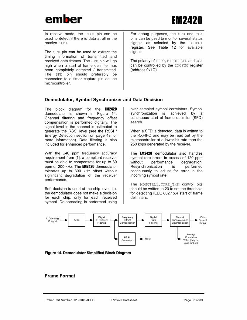
Demodulator, Symbol Synchronizer and Data Decision
The block diagram for the EM2420 demodulator is shown in Figure 14. Channel filtering and frequency offset compensation is performed digitally. The signal level in the channel is estimated to generate the RSSI level (see the RSSI / Energy Detection section on page 48 for more information). Data filtering is also included for enhanced performance.
With the ±40 ppm frequency accuracy requirement from [1], a compliant receiver must be able to compensate for up to 80 ppm or 200 kHz. The EM2420 demodulator tolerates up to 300 kHz offset without significant degradation of the receiver performance.
Soft decision is used at the chip level, i.e. the demodulator does not make a decision for each chip, only for each received symbol. De-spreading is performed using
over sampled symbol correlators. Symbol synchronization is achieved by a continuous start of frame delimiter (SFD) search.
When a SFD is detected, data is written to the RXFIFO and may be read out by the microcontroller at a lower bit rate than the 250 kbps generated by the receiver.
The EM2420 demodulator also handles symbol rate errors in excess of 120 ppm without performance degradation. Resynchronization is performed continuously to adjust for error in the incoming symbol rate.
The MDMCTRL1.CORR_THR control bits should be written to 20 to set the threshold for detecting IEEE 802.15.4 start of frame delimiters.
DigitalIF Channel
FilteringADC
DigitalData
Filtering
FrequencyOffset
Compensation
SymbolCorrelators andSynchronisation
RSSIGenerator
I / Q AnalogIF signal
DataSymbolOutput
RSSI
AverageCorrelation
Value (may beused for LQI)
Figure 14. Demodulator Simplified Block Diagram
Frame Format
EM2420
Ember Part Number: 120-0049-000C EM2420 Datasheet Page 34 of 89
The EM2420 has hardware support for parts of the IEEE 802.15.4 frame format. This section gives a brief summary to the IEEE 802.15.4 frame format, and describes how the EM2420 is set up to comply with this.
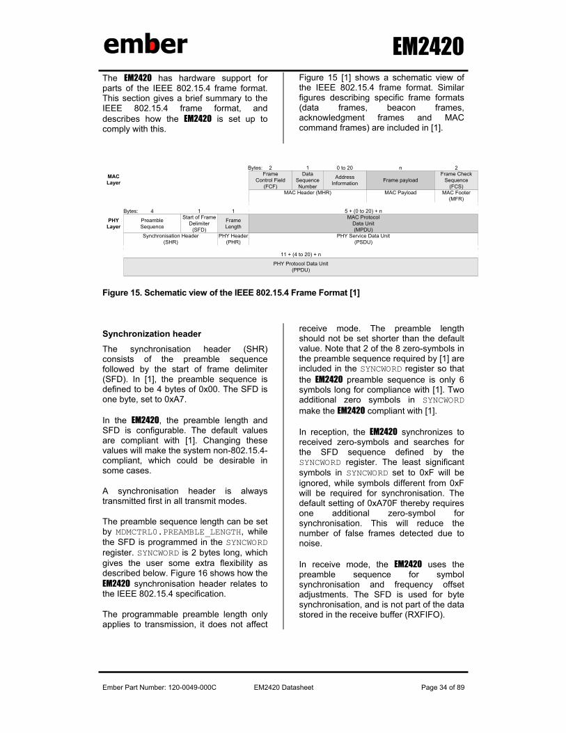
Figure 15 [1] shows a schematic view of the IEEE 802.15.4 frame format. Similar figures describing specific frame formats (data frames, beacon frames, acknowledgment frames and MAC command frames) are included in [1].
PHYLayer
FrameControl Field
(FCF)
DataSequenceNumber
2 1Bytes:
AddressInformation
0 to 20
Frame payload
nFrame Check
Sequence(FCS)
2
MAC Header (MHR) MAC Payload MAC Footer(MFR)
FrameLength
MAC ProtocolData Unit(MPDU)
Start of FrameDelimiter
(SFD)
Bytes: 1 1 5 + (0 to 20) + n
PreambleSequence
4
Synchronisation Header(SHR)
PHY Header(PHR)
PHY Service Data Unit(PSDU)
PHY Protocol Data Unit(PPDU)
11 + (4 to 20) + n
MACLayer
Figure 15. Schematic view of the IEEE 802.15.4 Frame Format [1]
Synchronization header
The synchronisation header (SHR) consists of the preamble sequence followed by the start of frame delimiter (SFD). In [1], the preamble sequence is defined to be 4 bytes of 0x00. The SFD is one byte, set to 0xA7.
In the EM2420, the preamble length and SFD is configurable. The default values are compliant with [1]. Changing these values will make the system non-802.15.4-compliant, which could be desirable in some cases.
A synchronisation header is always transmitted first in all transmit modes.
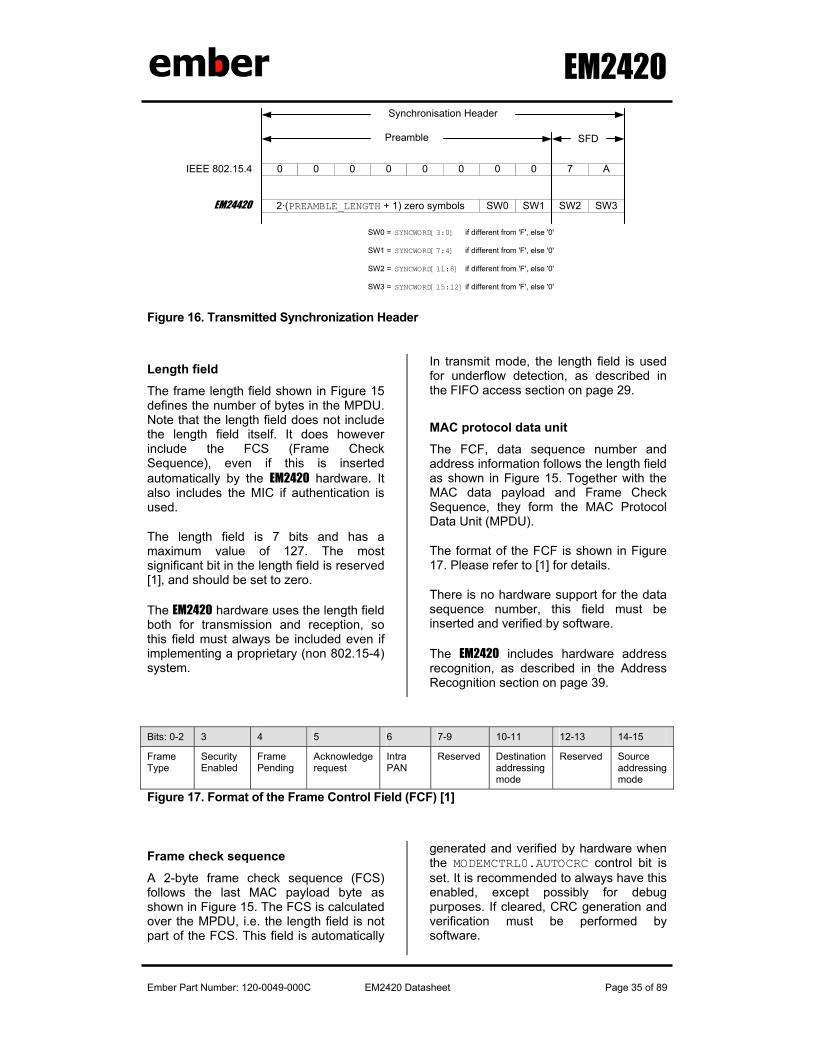
The preamble sequence length can be set by MDMCTRL0.PREAMBLE_LENGTH, while the SFD is programmed in the SYNCWORD register. SYNCWORD is 2 bytes long, which gives the user some extra flexibility as described below. Figure 16 shows how the EM2420 synchronisation header relates to the IEEE 802.15.4 specification.
The programmable preamble length only applies to transmission, it does not affect
receive mode. The preamble length should not be set shorter than the default value. Note that 2 of the 8 zero-symbols in the preamble sequence required by [1] are included in the SYNCWORD register so that the EM2420 preamble sequence is only 6 symbols long for compliance with [1]. Two additional zero symbols in SYNCWORD make the EM2420 compliant with [1].
In reception, the EM2420 synchronizes to received zero-symbols and searches for the SFD sequence defined by the SYNCWORD register. The least significant symbols in SYNCWORD set to 0xF will be ignored, while symbols different from 0xF will be required for synchronisation. The default setting of 0xA70F thereby requires one additional zero-symbol for synchronisation. This will reduce the number of false frames detected due to noise.
In receive mode, the EM2420 uses the preamble sequence for symbol synchronisation and frequency offset adjustments. The SFD is used for byte synchronisation, and is not part of the data stored in the receive buffer (RXFIFO).
EM2420
Ember Part Number: 120-0049-000C EM2420 Datasheet Page 35 of 89
0 7 AIEEE 802.15.4
Preamble SFD
EM24420 2·(PREAMBLE_LENGTH + 1) zero symbols
0 0 0 0 0 0 0
SW0
SW0 = SYNCWORD[3:0]
SW1 = SYNCWORD[7:4]
SW2 = SYNCWORD[11:8]
SW3 = SYNCWORD[15:12]
SW1 SW2 SW3
if different from 'F', else '0'
if different from 'F', else '0'
if different from 'F', else '0'
if different from 'F', else '0'
Synchronisation Header
Figure 16. Transmitted Synchronization Header
Length field
The frame length field shown in Figure 15 defines the number of bytes in the MPDU. Note that the length field does not include the length field itself. It does however include the FCS (Frame Check Sequence), even if this is inserted automatically by the EM2420 hardware. It also includes the MIC if authentication is used.
The length field is 7 bits and has a maximum value of 127. The most significant bit in the length field is reserved [1], and should be set to zero.
The EM2420 hardware uses the length field both for transmission and reception, so this field must always be included even if implementing a proprietary (non 802.15-4) system.
In transmit mode, the length field is used for underflow detection, as described in the FIFO access section on page 29.
MAC protocol data unit
The FCF, data sequence number and address information follows the length field as shown in Figure 15. Together with the MAC data payload and Frame Check Sequence, they form the MAC Protocol Data Unit (MPDU).
The format of the FCF is shown in Figure 17. Please refer to [1] for details.
There is no hardware support for the data sequence number, this field must be inserted and verified by software.
The EM2420 includes hardware address recognition, as described in the Address Recognition section on page 39.
Bits: 0-2 3 4 5 6 7-9 10-11 12-13 14-15
Frame Type
Security Enabled
Frame Pending
Acknowledge request
Intra PAN
Reserved Destination addressing mode
Reserved Source addressing mode
Figure 17. Format of the Frame Control Field (FCF) [1]
Frame check sequence
A 2-byte frame check sequence (FCS) follows the last MAC payload byte as shown in Figure 15. The FCS is calculated over the MPDU, i.e. the length field is not part of the FCS. This field is automatically
generated and verified by hardware when the MODEMCTRL0.AUTOCRC control bit is set. It is recommended to always have this enabled, except possibly for debug purposes. If cleared, CRC generation and verification must be performed by software.
EM2420
Ember Part Number: 120-0049-000C EM2420 Datasheet Page 36 of 89
The FCS polynomial is [1]:
x16 + x12 + x5 + 1
The EM2420 hardware implementation is shown in Figure 18. Please refer to [1] for further details.
In transmit mode the FCS is appended at the correct position defined by the length field. The FCS is not written to the TXFIFO, but stored in a separate 16-bit register.
In receive mode the FCS is verified by hardware. The user is normally only interested in the correctness of the FCS, not the FCS sequence itself. The FCS sequence itself is therefore not written to the RXFIFO during receive.
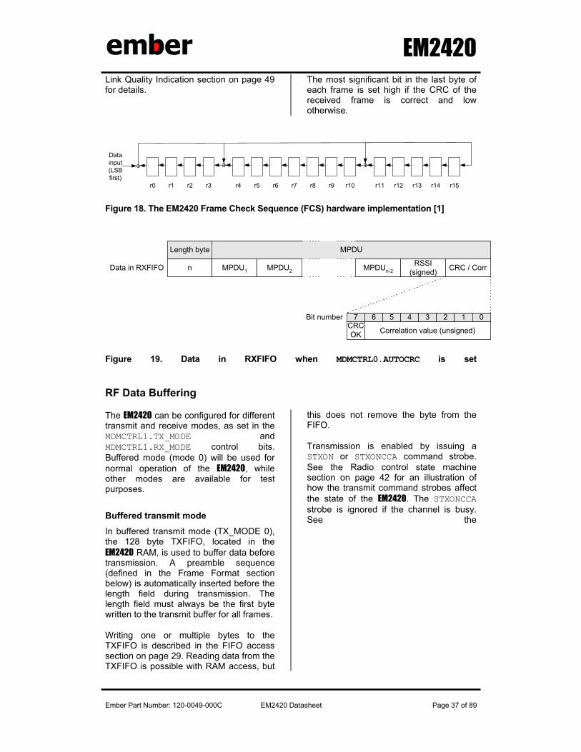
Instead, when MODEMCTRL0.AUTOCRC is set the two FCS bytes are replaced by the RSSI value, average correlation value (used for LQI) and CRC OK/not OK. This is illustrated in Figure 19.
The first FCS byte is replaced by the 8-bit RSSI value. See the RSSI section on page 48 for details.
The 7 least significant bits in the last FCS byte are replaced by the average correlation value of the 8 first symbols of the received PHY header (length field) and PHY Service Data Unit (PSDU). This correlation value may be used as a basis for calculating the LQI. See the
EM2420
Ember Part Number: 120-0049-000C EM2420 Datasheet Page 37 of 89
Link Quality Indication section on page 49 for details.
The most significant bit in the last byte of each frame is set high if the CRC of the received frame is correct and low otherwise.
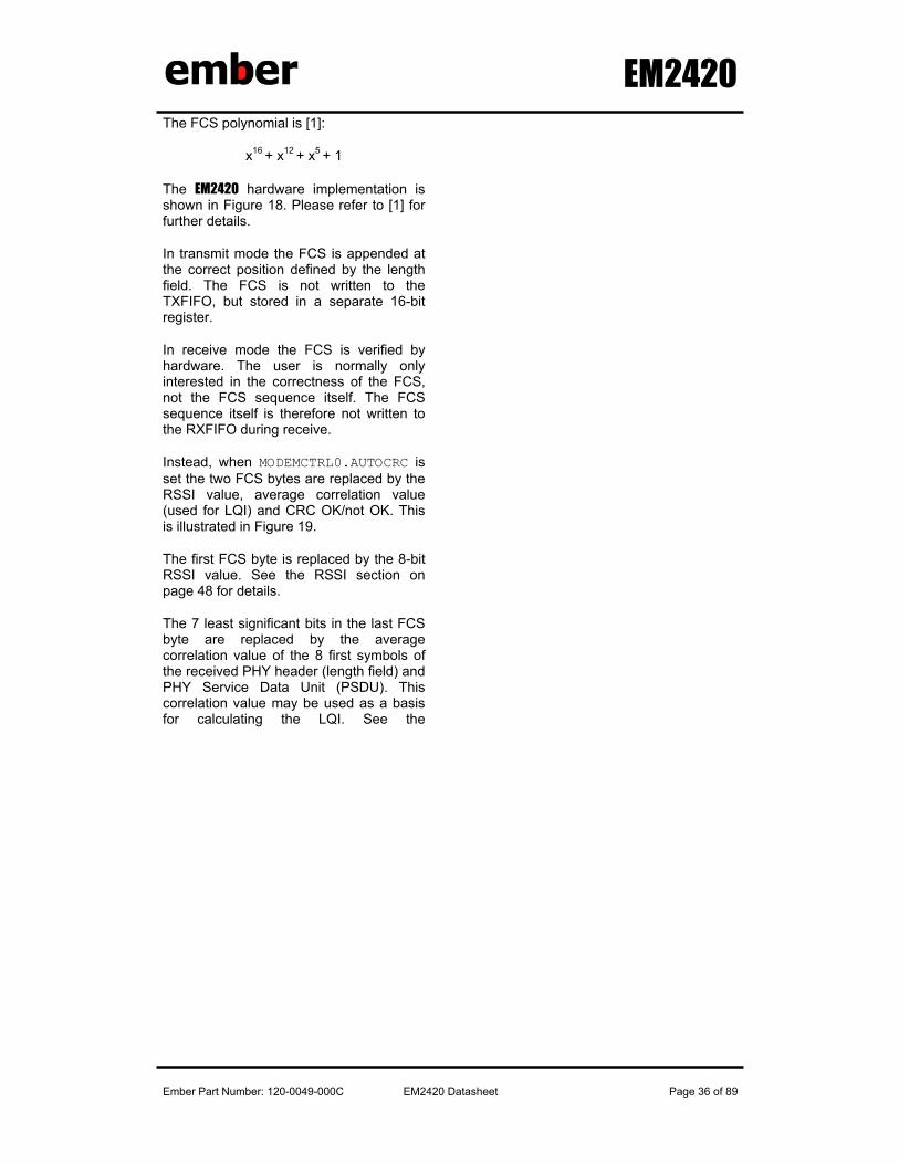
r0 r1 r2 r3 r4 r5 r6 r7 r8 r9 r10 r11 r12 r13 r14 r15
Datainput(LSBfirst)
Figure 18. The EM2420 Frame Check Sequence (FCS) hardware implementation [1]
MPDULength byte
n MPDU1 MPDU2 MPDUn-2RSSI
(signed) CRC / Corr
7 6 5 4 3 2 1 0Bit numberCRCOK Correlation value (unsigned)
Data in RXFIFO
Figure 19. Data in RXFIFO when MDMCTRL0.AUTOCRC is set
RF Data Buffering
The EM2420 can be configured for different transmit and receive modes, as set in the MDMCTRL1.TX_MODE and MDMCTRL1.RX_MODE control bits. Buffered mode (mode 0) will be used for normal operation of the EM2420, while other modes are available for test purposes.
Buffered transmit mode
In buffered transmit mode (TX_MODE 0), the 128 byte TXFIFO, located in the EM2420 RAM, is used to buffer data before transmission. A preamble sequence (defined in the Frame Format section below) is automatically inserted before the length field during transmission. The length field must always be the first byte written to the transmit buffer for all frames.
Writing one or multiple bytes to the TXFIFO is described in the FIFO access section on page 29. Reading data from the TXFIFO is possible with RAM access, but
this does not remove the byte from the FIFO.
Transmission is enabled by issuing a STXON or STXONCCA command strobe. See the Radio control state machine section on page 42 for an illustration of how the transmit command strobes affect the state of the EM2420. The STXONCCA strobe is ignored if the channel is busy. See the
EM2420
Ember Part Number: 120-0049-000C EM2420 Datasheet Page 38 of 89
Clear Channel Assessment section on page 50 for details on CCA.
The preamble sequence is started 12 symbol periods after the command strobe. After the programmable start of frame delimiter has been transmitted, data is fetched from the TXFIFO.
A TXFIFO underflow is issued if too few bytes are written to the TXFIFO. Transmission is then automatically stopped. The underflow is indicated in the TX_UNDERFLOW status bit, which is returned during each address byte and each byte written to the TXFIFO. The underflow bit is only cleared by issuing a SFLUSHTX command strobe.
The TXFIFO can only contain one data frame at a given time.
After complete transmission of a data frame, the TXFIFO is automatically refilled with the last transmitted frame. Issuing a new STXON or STXONCCA command strobe will then cause the EM2420 to retransmit the last frame.
Writing to the TXFIFO after a frame has been transmitted will cause the TXFIFO to be automatically flushed before the new byte is written. The only exception is if a TXFIFO underflow has occurred, when a SFLUSHTX command strobe is required.
Buffered receive mode
In buffered receive mode (RX_MODE 0), the 128 byte RXFIFO, located in the EM2420 RAM, is used to buffer data received by the demodulator. Accessing data in the RXFIFO is described in the FIFO access section on page 29.
The FIFO and FIFOP pins are used to assist the microcontroller in supervising the RXFIFO. Please note that the FIFO and FIFOP pins are only related to the RXFIFO, even if the EM2420 is in transmit mode.
Multiple data frames may be in the RXFIFO simultaneously, as long as the total number of bytes does not exceed 128.
See the RXFIFO overflow section on page 31 for details on how a RXFIFO overflow is detected and signaled.
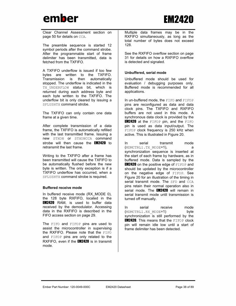
Unbuffered, serial mode
Unbuffered mode should be used for evaluation / debugging purposes only. Buffered mode is recommended for all applications.
In un-buffered mode, the FIFO and FIFOP pins are reconfigured as data and data clock pins. The TXFIFO and RXFIFO buffers are not used in this mode. A synchronous data clock is provided by the EM2420 at the FIFOP pin, and the FIFO pin is used as data input/output. The FIFOP clock frequency is 250 kHz when active. This is illustrated in Figure 20.
In serial transmit mode (MDMCTRL1.TX_MODE=1), a synchronization sequence is inserted at the start of each frame by hardware, as in buffered mode. Data is sampled by the EM2420 on the positive edge of FIFOP and should be updated by the microcontroller on the negative edge of FIFOP. See Figure 20 for an illustration of the timing in serial transmit mode. The SFD and CCA pins retain their normal operation also in serial mode. The EM2420 will remain in serial transmit mode until transmission is turned off manually.
In serial receive mode (MDMCTRL1.RX_MODE=1) byte synchronization is still performed by the EM2420. This means that the FIFOP clock pin will remain idle low until a start of frame delimiter has been detected.
EM2420
Ember Part Number: 120-0049-000C EM2420 Datasheet Page 39 of 89
Receive mode:
Incoming / outgoingRF data SFD
FIFOP
Transmit mode:
Preamble
FIFO (from uC) b0 b1 b2 b3 b4 b5 b6 b7 b8 b9 b10 b11
s0 s1
FIFOP
FIFO (from EM2420) b0 b1 b2 b3 b4
s2
b8 b9 b10 b11
4 us
Figure 20. Unbuffered test mode, pin activity
Address Recognition
The EM2420 includes hardware support for address recognition, as specified in [1]. Hardware address recognition may be enabled / disabled using the MDMCTRL0.ADR_DECODE control bit.
Address recognition is based on the following requirements, listed from section 7.5.6.2 in [1]:
• The frame type subfield shall not contain an illegal frame type
• If the frame type indicates that the frame is a beacon frame, the source PAN identifier shall match macPANId unless macPANId is equal to 0xFFFF, in which case the beacon frame shall be accepted regardless of the source PAN identifier.
• If a destination PAN identifier is included in the frame, it shall match macPANId or shall be the broadcast PAN identifier (0xFFFF).
• If a short destination address is included in the frame, it shall match either macShortAddress or the broadcast address (0xFFFF). Otherwise if an extended destination address is included in the frame, it shall match aExtendedAddress.
• If only source addressing fields are included in a data or MAC command frame, the frame shall only be accepted if the device is a PAN coordinator and the source PAN identifier matches macPANId.
If any of the above requirements are not satisfied and address recognition is enabled, the EM2420 will disregard the incoming frame and flush the data from the RXFIFO. Only data from the rejected frame is flushed, data from previously accepted frames may still be in the RXFIFO.
Incoming frames with reserved frame types (FCF frame type subfield is 4, 5, 6 or 7) is however accepted if the RESERVED_FRAME_MODE control bit in MDMCTRL0 is set. In this case, no further address recognition is performed on these frames. This option is included for future expansions of the IEEE 802.15.4 standard.
If a frame is rejected, the EM2420 will only start searching for a new frame after the rejected frame has been completely received (as defined by the length field) to avoid detecting false SFDs within the frame.
The MDMCTRL0.PAN_COORDINATOR control bit must be correctly set, since parts of the address recognition procedure
EM2420
Ember Part Number: 120-0049-000C EM2420 Datasheet Page 40 of 89
requires knowledge about whether the current device is a PAN coordinator or not.
Acknowledge Frames
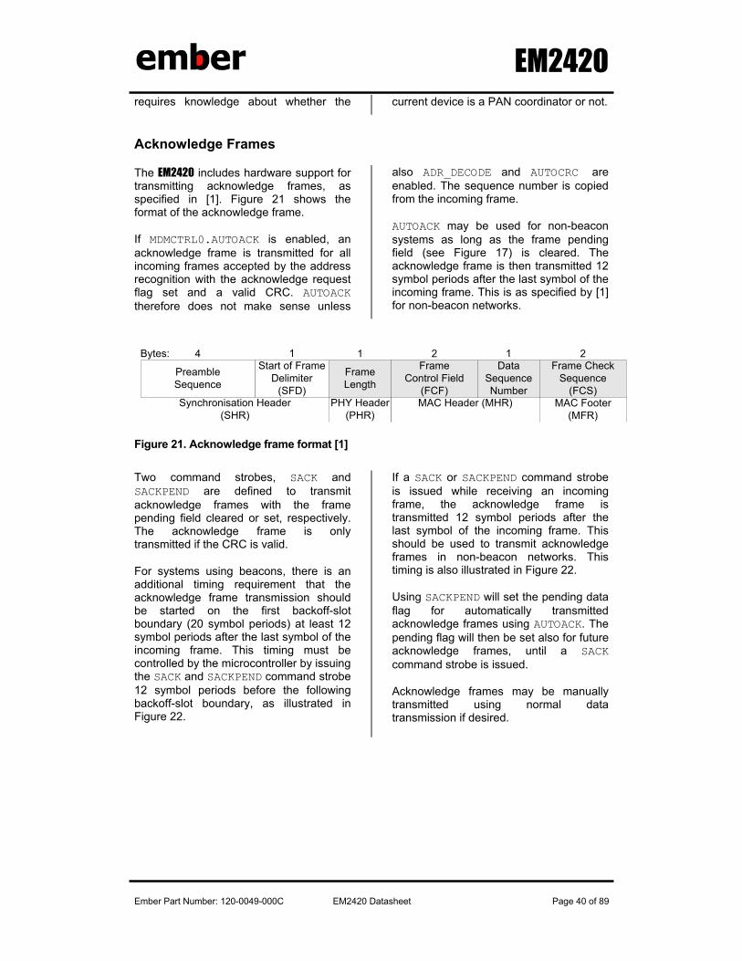
The EM2420 includes hardware support for transmitting acknowledge frames, as specified in [1]. Figure 21 shows the format of the acknowledge frame.
If MDMCTRL0.AUTOACK is enabled, an acknowledge frame is transmitted for all incoming frames accepted by the address recognition with the acknowledge request flag set and a valid CRC. AUTOACK therefore does not make sense unless
also ADR_DECODE and AUTOCRC are enabled. The sequence number is copied from the incoming frame.
AUTOACK may be used for non-beacon systems as long as the frame pending field (see Figure 17) is cleared. The acknowledge frame is then transmitted 12 symbol periods after the last symbol of the incoming frame. This is as specified by [1] for non-beacon networks.
FrameControl Field
(FCF)
DataSequenceNumber
2 1Frame Check
Sequence(FCS)
2
MAC Header (MHR) MAC Footer(MFR)
FrameLength
Start of FrameDelimiter
(SFD)
Bytes: 1 1
PreambleSequence
4
Synchronisation Header(SHR)
PHY Header(PHR)
Figure 21. Acknowledge frame format [1]
Two command strobes, SACK and SACKPEND are defined to transmit acknowledge frames with the frame pending field cleared or set, respectively. The acknowledge frame is only transmitted if the CRC is valid.
For systems using beacons, there is an additional timing requirement that the acknowledge frame transmission should be started on the first backoff-slot boundary (20 symbol periods) at least 12 symbol periods after the last symbol of the incoming frame. This timing must be controlled by the microcontroller by issuing the SACK and SACKPEND command strobe 12 symbol periods before the following backoff-slot boundary, as illustrated in Figure 22.
If a SACK or SACKPEND command strobe is issued while receiving an incoming frame, the acknowledge frame is transmitted 12 symbol periods after the last symbol of the incoming frame. This should be used to transmit acknowledge frames in non-beacon networks. This timing is also illustrated in Figure 22.
Using SACKPEND will set the pending data flag for automatically transmitted acknowledge frames using AUTOACK. The pending flag will then be set also for future acknowledge frames, until a SACK command strobe is issued.
Acknowledge frames may be manually transmitted using normal data transmission if desired.
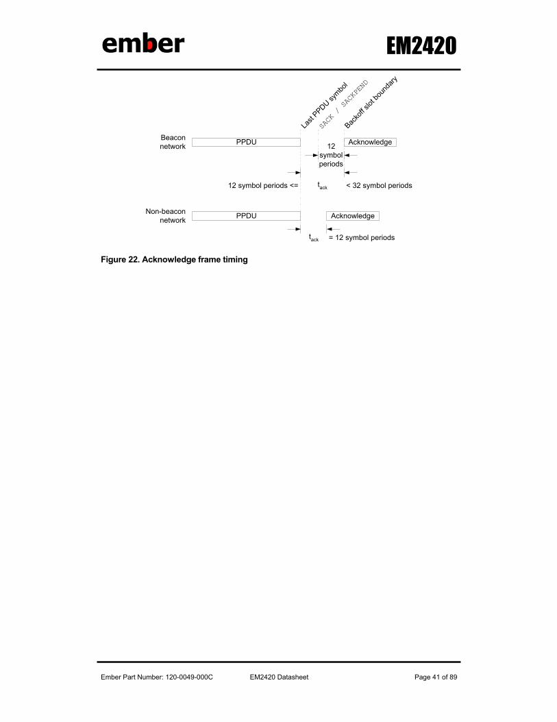
EM2420
Ember Part Number: 120-0049-000C EM2420 Datasheet Page 41 of 89
PPDU AcknowledgeNon-beaconnetwork
tack = 12 symbol periods
PPDU AcknowledgeBeaconnetwork
tack < 32 symbol periods12 symbol periods <=
Last
PPDU symbo
l
Backo
ff slot
boun
dary
12symbolperiods
SACK / SACKPEND
Figure 22. Acknowledge frame timing
EM2420
Ember Part Number: 120-0049-000C EM2420 Datasheet Page 42 of 89
Radio control state machine
The EM2420 has a built-in state machine that is used to switch between different operation states (modes). The change of state is done either by using command strobes or by internal events such as SFD detected in receive mode.
The radio control state machine states are shown in Figure 23. The numbers in brackets refer to the state number readable in the FSMSTATE status register. This functionality is primarily for test / debug purposes.
Before using the radio in either RX or TX mode, the voltage regulator and crystal oscillator must be turned on and become stable. The voltage regulator and crystal oscillator startup times are given in the Electrical Specifications section on page 9.
The crystal oscillator is controlled by accessing the SXOSCON / SXOSCOFF command strobes. The XOSC16M_STABLE bit in the status register returned during address transfer indicates whether the oscillator is running and stable or not (see Table 5). This status register can be polled when waiting for the oscillator to start.
For test purposes, the frequency synthesizer (FS) can also be manually calibrated and started by using the STXCAL command strobe register. This will not start a transmission before a STXON command strobe is issued. This is not shown in Figure 23.
Enabling transmission is done by issuing a STXON or STXONCCA command strobe.
Turning off RF can be accomplished by using one of the SRFOFF or SXOSCOFF command strobe registers.
After reset, the EM2420 is in Power Down mode. All configuration registers can then be programmed in order to make the chip ready to operate at the correct frequency and mode. Due to the very fast start-up time, the EM2420 can remain in Power Down until a transmission session is requested.
As also described in the 4-wire Serial Configuration and Data Interface section on page 25, the crystal oscillator must be running in order to have access to the RAM and FIFOs.
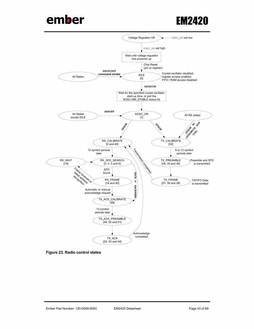
EM2420
Ember Part Number: 120-0049-000C EM2420 Datasheet Page 43 of 89
Wait for the specified crystal oscillatorstart-up time, or poll the
XOSC16M_STABLE status bit
IDLE[0]
SXOSCON
STXON
XOSC_ON[1]
Wait until voltage regulatorhas powered up
Voltage Regulator Off VREG_EN set low
VREG_EN set high
Chip Reset(pin or register)
All States
SXOSCOFFcommand strobe
All Statesexcept IDLE
SRFOFF
TX_CALIBRATE[32]
All RX states
TX_PREAMBLE[34, 35 and 36]
8 or 12 symbolperiods later
Preamble and SFDis transmitted
TX_FRAME[37, 38 and 39]
TXFIFO Datais transmitted
RX_CALIBRATE[2 and 40]
Transmission com
pleted
SRXON
RX_SFD_SEARCH[3, 4, 5 and 6]
RX_FRAME[16 and 40]
12 symbol periodslater
SFDfound
Frame received or
failed address
recognition
Automatic or manualacknowledge request
TX_ACK_CALIBRATE[48]
12 symbolperiods later
TX_ACK_PREAMBLE[49, 50 and 51]
TX_ACK[52, 53 and 54]
Acknowledgecompleted
RX_WAIT[14]
Crystal oscillator disabled,register access enabled,FIFO / RAM access disabled
STXON
or
(STXONCCA and
CCA)
SACK or
SACKPEND
Figure 23. Radio control states
EM2420
Ember Part Number: 120-0049-000C EM2420 Datasheet Page 44 of 89
MAC Security Operations (Encryption and Authentication)
The EM2420 features hardware IEEE 802.15.4 MAC security operations, which are exposed in the EmberNet API. This includes counter mode (CTR) encryption / decryption, CBC-MAC authentication and CCM encryption + authentication. All security operations are based on AES encryption [2] using 128 bit keys. Security operations are performed within the transmit and receive FIFOs on a frame basis.
The EM2420 also includes stand-alone AES encryption, in which one 128 bit plaintext is encrypted to a 128 bit ciphertext.
The SAES, STXENC and SRXDEC command strobes are used to start security operations in the EM2420 as will be described in the following sections. The ENC_BUSY status bit (see Table 5) may be used to monitor when a security operation has been completed. Security command strobes issued while the security engine is busy will be ignored, and the ongoing operation will be completed.
Table 6 on page 29 shows the EM2420 RAM memory map, including the security related data located from addresses 0x100 through 0x15F. RAM access (see the RAM access section on page 27) is used to write or read the keys, nonces, and stand-alone buffer. All security related data is stored little-endian, i.e. the least significant byte is transferred first over the SPI interface during RAM read or write operations.
For a complete description of IEEE 802.15.4 MAC security operations, please refer to [1].
Keys
All security operations are based on 128 bit keys. The EM2420 RAM space has storage space for two individual keys (KEY0 and KEY1). Transmit, receive and stand-alone encryption may select one of these two keys individually in the SEC_TXKEYSEL, SEC_RXKEYSEL and SEC_SAKEYSEL control bits (SECCTRL0).
As can be seen from Table 6 on page 29, KEY0 is located from address 0x100 and KEY1 from address 0x130.
A way of establishing the keys used for encryption and authentication must be decided for each particular application. IEEE 802.15.4 does not define how this is done; it is left to the higher layer of the protocol.
ZigBee uses an Eliptic Curve Cryptography (ECC) based approach to establish keys. For PC based solutions, more processor intensive solutions such as Diffie-Hellman may be chosen. Some applications may also use pre-programmed keys, e.g. for remote keyless entry where the key and lock are delivered in pairs. A push-button approach for loading keys may also be selected.
Nonce / counter
The receive and transmit nonces used for encryption / decryption are located in RAM from addresses 0x110 and 0x140 respectively. They are both 16 bytes.
The nonce must be correctly initialized before receive or transmit CTR or CCM operations are started. The format of the nonce is shown in Table 7. The block counter must be set to 1 for compliance with [1]. The key sequence counter is controlled by a layer above the MAC layer. The frame counter must be increased for each new frame by the MAC layer. The source address is the 64 bit IEEE address.
1 byte 8 bytes 4 bytes 1 byte 2 bytes
Flags Source Address
Frame Counter
Key Sequence Counter
Block Counter
Table 7. IEEE 802.15.4 Nonce [1]
The block counter bytes are not updated in RAM, only in a local copy which is reloaded for each new in-line security operation. I.e. the block counter part of the nonce does not need to be rewritten. The EM2420 block counter should be set to 0x0001 for compliance with [1].
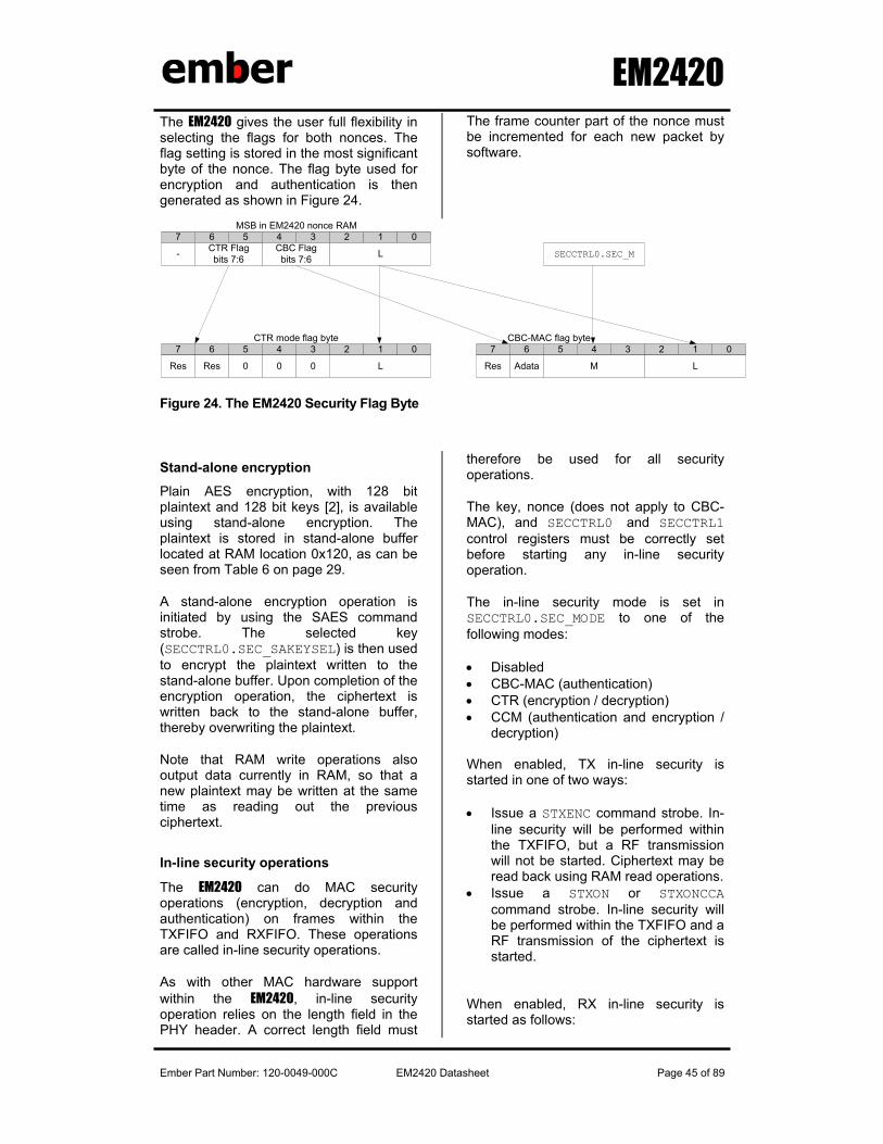
EM2420
Ember Part Number: 120-0049-000C EM2420 Datasheet Page 45 of 89
The EM2420 gives the user full flexibility in selecting the flags for both nonces. The flag setting is stored in the most significant byte of the nonce. The flag byte used for encryption and authentication is then generated as shown in Figure 24.
The frame counter part of the nonce must be incremented for each new packet by software.
7 6CTR Flagbits 7:6
5 4 3 2 1 0
- CBC Flagbits 7:6 L
7 6
Res
5 4 3 2 1 0
L
7 6
Adata
5 4 3 2 1 0
M L0 0 0
SECCTRL0.SEC_M
MSB in EM2420 nonce RAM
CTR mode flag byte CBC-MAC flag byte
Res Res
Figure 24. The EM2420 Security Flag Byte
Stand-alone encryption
Plain AES encryption, with 128 bit plaintext and 128 bit keys [2], is available using stand-alone encryption. The plaintext is stored in stand-alone buffer located at RAM location 0x120, as can be seen from Table 6 on page 29.
A stand-alone encryption operation is initiated by using the SAES command strobe. The selected key (SECCTRL0.SEC_SAKEYSEL) is then used to encrypt the plaintext written to the stand-alone buffer. Upon completion of the encryption operation, the ciphertext is written back to the stand-alone buffer, thereby overwriting the plaintext.
Note that RAM write operations also output data currently in RAM, so that a new plaintext may be written at the same time as reading out the previous ciphertext.
In-line security operations
The EM2420 can do MAC security operations (encryption, decryption and authentication) on frames within the TXFIFO and RXFIFO. These operations are called in-line security operations.
As with other MAC hardware support within the EM2420, in-line security operation relies on the length field in the PHY header. A correct length field must
therefore be used for all security operations.
The key, nonce (does not apply to CBC-MAC), and SECCTRL0 and SECCTRL1 control registers must be correctly set before starting any in-line security operation.
The in-line security mode is set in SECCTRL0.SEC_MODE to one of the following modes:
• Disabled • CBC-MAC (authentication) • CTR (encryption / decryption) • CCM (authentication and encryption /
decryption) When enabled, TX in-line security is started in one of two ways:
• Issue a STXENC command strobe. In-line security will be performed within the TXFIFO, but a RF transmission will not be started. Ciphertext may be read back using RAM read operations.
• Issue a STXON or STXONCCA command strobe. In-line security will be performed within the TXFIFO and a RF transmission of the ciphertext is started.
When enabled, RX in-line security is started as follows:
EM2420
Ember Part Number: 120-0049-000C EM2420 Datasheet Page 46 of 89
• Issue a SRXDEC command strobe. The first frame in the RXFIFO is then decrypted / authenticated as set by the current security mode.
RX in-line security operations are always performed on the first frame currently inside the RXFIFO, even if part of this has already been read out over the SPI interface. This allows the receiver to first read the source address out to decide which key to use before doing authentication of the complete frame. In CTR or CCM mode it is of course important that bytes to be decrypted are not read out before the security operation is started.
When the SRXDEC command strobe is issued, the FIFO and FIFOP pins will go low. This is to indicate to the microcontroller that no further data may be read out before the next byte to be read has undergone the requested security operation.
The frame in the RXFIFO may be received over RF or it may be written into the RXFIFO over the SPI interface for debugging or higher layer security operations.
CTR mode encryption / decryption
CTR mode encryption / decryption is performed by the EM2420 on MAC frames within the TXFIFO / RXFIFO respectively.
SECCTRL1.SEC_TXL / SEC_RXL sets the number of bytes between the length field and the first byte to be encrypted / decrypted respectively. This controls the number of plaintext bytes in the current frame. For IEEE 802.15.4 MAC encryption, only the MAC payload (see Figure 15 on page 34) should be encrypted, so SEC_TXL / SEC_RXL is set to 3 + (0 to 20) depending on the address information in the current frame.
When encryption is initiated, the plaintext in the TXFIFO is then encrypted as specified by [1]. The encryption module will encrypt all the plaintext currently available, and wait if not everything is prebuffered. The encryption operation may also be started without any data in the
TXFIFO at all, and data will be encrypted as it is written to the TXFIFO.
When decryption is initiated with a SRXDEC command strobe, the ciphertext of the RXFIFO is then decrypted as specified by [1].
CBC-MAC
CBC-MAC in-line authentication is provided by the EM2420 hardware.
SECCTRL0.SEC_M sets the MIC length M, encoded as (M-2)/2.
When enabling CBC-MAC in-line TXFIFO authentication, the generated MIC is written to the TXFIFO for transmission. The frame length must include the MIC.
SECCTRL1.SEC_TXL / SEC_RXL sets the number of bytes between the length field and the first byte to be authenticated, normally set to 0 for MAC authentication.
SECCTRL0.SEC_CBC_HEAD defines if the authentication length is used as the first byte of data to be authenticated or not. This bit should be set for compliance with [1].
When enabling CBC-MAC in-line RXFIFO authentication, the generated MIC is compared to the MIC in the RXFIFO. The last byte of the MIC is replaced in the RXFIFO with:
• 0x00 if the MIC is correct
• 0xFF if the MIC is incorrect
The other bytes in the MIC are left unchanged in the RXFIFO.
CCM
CCM combines CTR mode encryption and CBC-MAC authentication in one operation. CCM is described in [3].
SECCTRL1.SEC_TXL / SEC_RXL sets the number of bytes after the length field to be authenticated but not encrypted.
The MIC is generated and verified very much like with CBC-MAC described
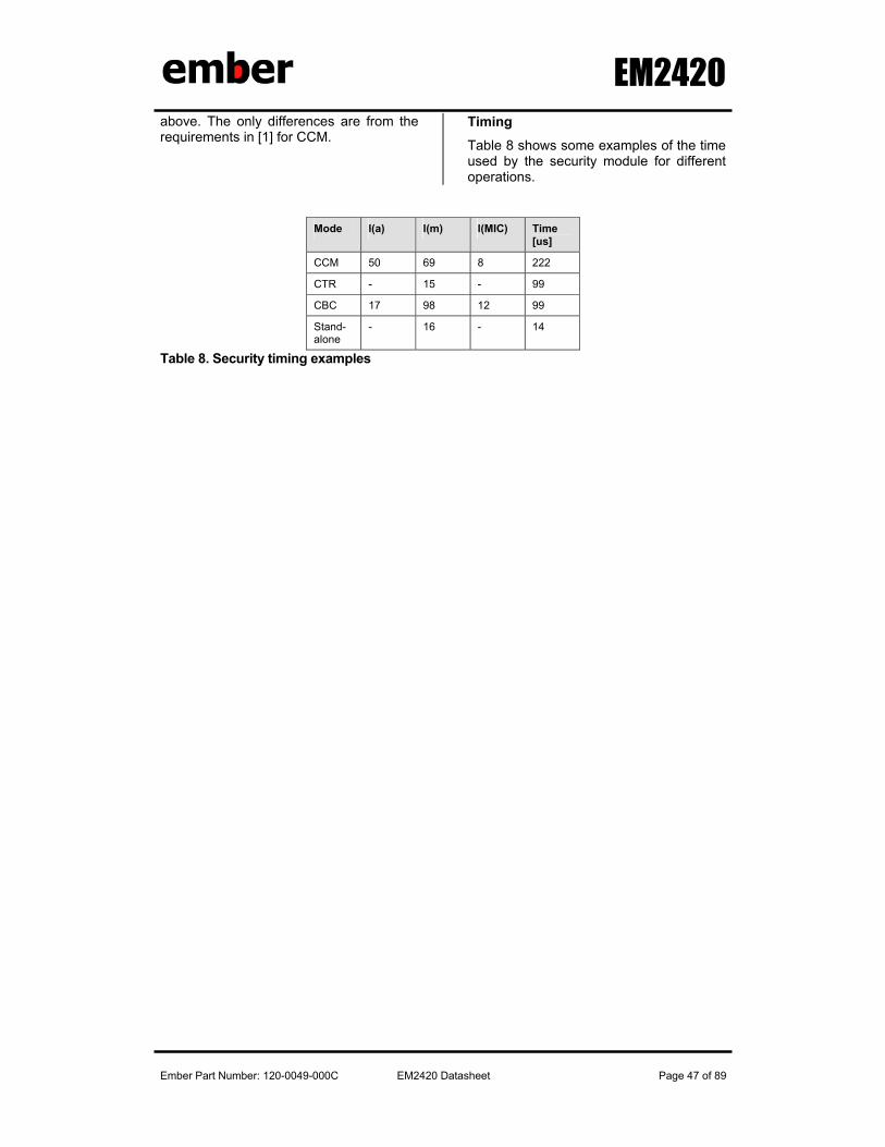
EM2420
Ember Part Number: 120-0049-000C EM2420 Datasheet Page 47 of 89
above. The only differences are from the requirements in [1] for CCM.
Timing
Table 8 shows some examples of the time used by the security module for different operations.
Mode l(a) l(m) l(MIC) Time [us]
CCM 50 69 8 222
CTR - 15 - 99
CBC 17 98 12 99
Stand- alone
- 16 - 14
Table 8. Security timing examples
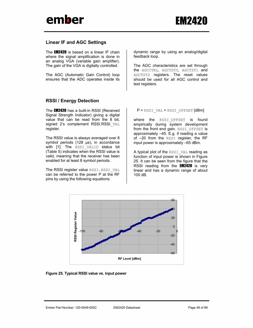
EM2420
Ember Part Number: 120-0049-000C EM2420 Datasheet Page 48 of 89
Linear IF and AGC Settings
The EM2420 is based on a linear IF chain where the signal amplification is done in an analog VGA (variable gain amplifier). The gain of the VGA is digitally controlled.
The AGC (Automatic Gain Control) loop ensures that the ADC operates inside its
dynamic range by using an analog/digital feedback loop.
The AGC characteristics are set through the AGCCTRL, AGCTST0, AGCTST1 and AGCTST2 registers. The reset values should be used for all AGC control and test registers.
RSSI / Energy Detection
The EM2420 has a built-in RSSI (Received Signal Strength Indicator) giving a digital value that can be read from the 8 bit, signed 2’s complement RSSI.RSSI_VAL register.
The RSSI value is always averaged over 8 symbol periods (128 µs), in accordance with [1]. The RSSI_VALID status bit (Table 5) indicates when the RSSI value is valid, meaning that the receiver has been enabled for at least 8 symbol periods.
The RSSI register value RSSI.RSSI_VAL can be referred to the power P at the RF pins by using the following equations:
P = RSSI_VAL + RSSI_OFFSET [dBm]
where the RSSI_OFFSET is found empirically during system development from the front end gain. RSSI_OFFSET is approximately –45. E.g. if reading a value of –20 from the RSSI register, the RF input power is approximately –65 dBm.
A typical plot of the RSSI_VAL reading as function of input power is shown in Figure 25. It can be seen from the figure that the RSSI reading from the EM2420 is very linear and has a dynamic range of about 100 dB.
-60
-40
-20
0
20
40
60
-100 -80 -60 -40 -20 0
RF Level [dBm]
RSS
I Reg
iste
r Val
ue
Figure 25. Typical RSSI value vs. input power
EM2420
Ember Part Number: 120-0049-000C EM2420 Datasheet Page 49 of 89
Link Quality Indication
The link quality indication (LQI) measurement is a characterization of the strength and/or quality of a received packet, as defined by [1].
The RSSI value described in the previous section may be used by the MAC software to produce the LQI value. The LQI value is required by [1] to be limited to the range 0 through 255, with at least 8 unique values. Software is responsible for generating the appropriate scaling of the LQI value for the given application.
Using the RSSI value directly to calculate the LQI value has the disadvantage that e.g. a narrowband interferer inside the channel bandwidth will increase the LQI value although it actually reduces the true link quality. The EM2420 therefore also provides an average correlation value for each incoming packet, based on the 8 first symbols following the SFD. This unsigned 7-bit value can be looked upon as a measurement of the “chip error rate,” although the EM2420 does not do chip decision.
As described in the Frame check sequence section on page 35, the average correlation value for the 8 first symbols is appended to each received frame together with the RSSI and CRC OK/not OK when MDMCTRL0.AUTOCRC is set. A correlation value of ~110 indicates a maximum quality frame while a value of ~50 is typically the lowest quality frames detectable by the EM2420.
Software must convert the correlation value to the range 0-255 defined by [1], e.g. by calculating:
LQI = (CORR – a) · b
limited to the range 0-255, where a and b are found empirically based on PER measurements as a function of the correlation value.
A combination of RSSI and correlation values may also be used to generate the LQI value.
EM2420
Ember Part Number: 120-0049-000C EM2420 Datasheet Page 50 of 89
Clear Channel Assessment
The clear channel assessment signal is based on the measured RSSI value and a programmable threshold. The clear channel assessment function is used to implement the CSMA-CA functionality specified in [1]. CCA is valid when the receiver has been enabled for at least 8 symbol periods.
Carrier sense threshold level is programmed by RSSI.CCA_THR. The threshold value can be programmed in steps of 1 dB. A CCA hysteresis can also be programmed in the MDMCTRL0.CCA_HYST control bits.
All 3 CCA modes specified by [1] are implemented in the EM2420. They are set in MDMCTRL0.CCA_MODE, as can be seen in the register description. The different modes are:
0 Reserved
1 Clear channel when received energy is below threshold.
2 Clear channel when not receiving valid IEEE 802.15.4 data.
3 Clear channel when energy is below threshold and not receiving valid IEEE 802.15.4 data
Clear channel assessment is available on the CCA output pin. CCA is active high, but the polarity may be changed by setting the IOCFG0.CCA_POLARITY control bit.
Implementing CSMA-CA may easiest be done by using the STXONCCA command strobe, as described in the Radio control state machine section on page 42. Transmission will then only start if the channel is clear. The TX_ACTIVE status bit (see Table 5) may be used to detect the result of the CCA.
EM2420
Ember Part Number: 120-0049-000C EM2420 Datasheet Page 51 of 89
Frequency and Channel Programming
The operating frequency is set by programming the 10 bit frequency word located in FSCTRL.FREQ[9:0]. The operating frequency FC in MHz is given by:
FC = 2048 + FSCTRL.FREQ[9:0] MHz
In receive mode the actual LO frequency is FC – 2 MHz, since a 2 MHz IF is used. Direct conversion is used for transmission, so here the LO frequency equals FC. The 2 MHz IF is automatically set by the EM2420, so the frequency programming is equal for RX and TX.
IEEE 802.15.4 specifies 16 channels within the 2.4 GHz band, numbered 11 through 26. The RF frequency of channel k is given by [1]:
FC = 2405 + 5 (k-11) MHz, k=11, 12, ..., 26
For operation in channel k, the FSCTRL.FREQ register should therefore be set to:
FSCTRL.FREQ = 357 + 5 (k-11)
VCO and PLL Self-Calibration
VCO
The VCO is completely integrated and operates at 4800 – 4966 MHz. The VCO frequency is divided by 2 to generate frequencies in the desired band (2400-2483.5 MHz).
PLL self-calibration
The VCO's characteristics will vary with temperature, changes in supply voltages, and the desired operating frequency.
In order to ensure reliable operation the VCO’s bias current and tuning range are automatically calibrated every time the RX mode or TX mode is enabled, i.e. in the RX_CALIBRATE, TX_CALIBRATE and TX_ACK_CALIBRATE control states in Figure 23 on page 43.
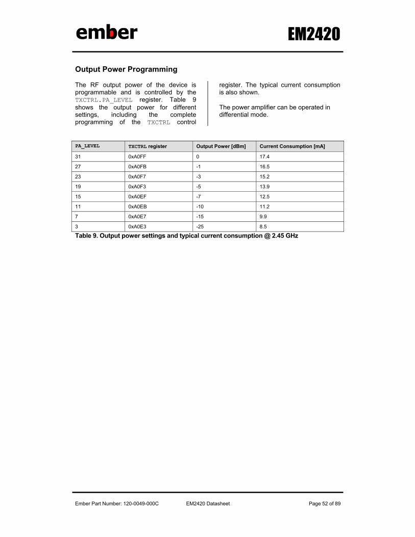
EM2420
Ember Part Number: 120-0049-000C EM2420 Datasheet Page 52 of 89
Output Power Programming
The RF output power of the device is programmable and is controlled by the TXCTRL.PA_LEVEL register. Table 9 shows the output power for different settings, including the complete programming of the TXCTRL control
register. The typical current consumption is also shown.
The power amplifier can be operated in differential mode.
PA_LEVEL TXCTRL register Output Power [dBm] Current Consumption [mA]
31 0xA0FF 0 17.4
27 0xA0FB -1 16.5
23 0xA0F7 -3 15.2
19 0xA0F3 -5 13.9
15 0xA0EF -7 12.5
11 0xA0EB -10 11.2
7 0xA0E7 -15 9.9
3 0xA0E3 -25 8.5
Table 9. Output power settings and typical current consumption @ 2.45 GHz
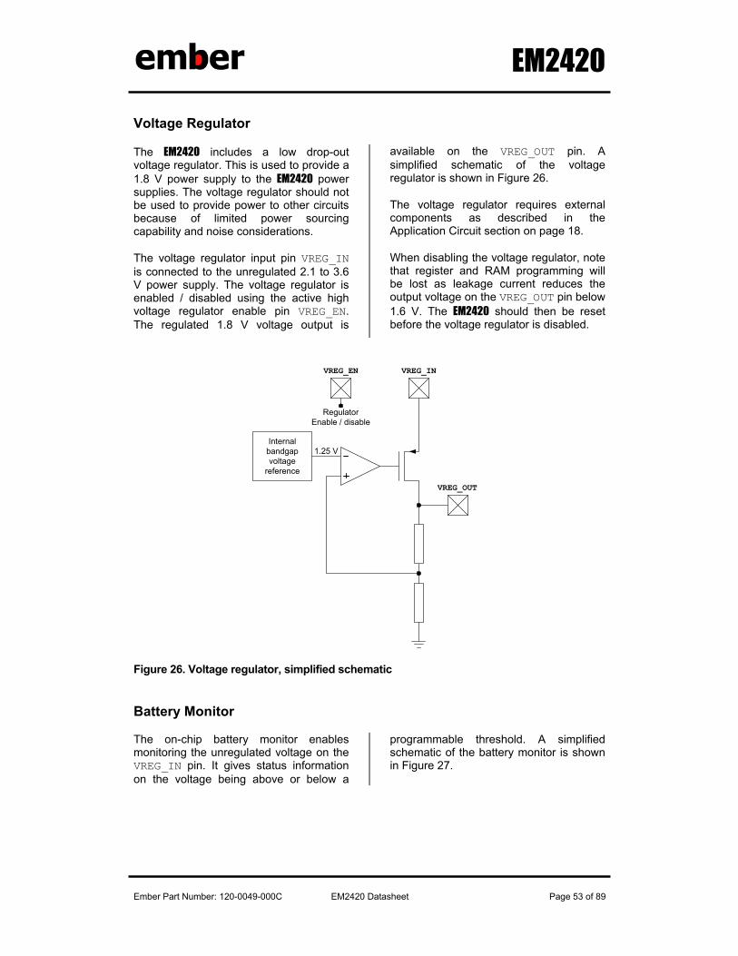
EM2420
Ember Part Number: 120-0049-000C EM2420 Datasheet Page 53 of 89
Voltage Regulator
The EM2420 includes a low drop-out voltage regulator. This is used to provide a 1.8 V power supply to the EM2420 power supplies. The voltage regulator should not be used to provide power to other circuits because of limited power sourcing capability and noise considerations.
The voltage regulator input pin VREG_IN is connected to the unregulated 2.1 to 3.6 V power supply. The voltage regulator is enabled / disabled using the active high voltage regulator enable pin VREG_EN. The regulated 1.8 V voltage output is
available on the VREG_OUT pin. A simplified schematic of the voltage regulator is shown in Figure 26.
The voltage regulator requires external components as described in the Application Circuit section on page 18.
When disabling the voltage regulator, note that register and RAM programming will be lost as leakage current reduces the output voltage on the VREG_OUT pin below 1.6 V. The EM2420 should then be reset before the voltage regulator is disabled.
VREG_IN
Internalbandgapvoltage
reference
1.25 V
VREG_OUT
VREG_EN
RegulatorEnable / disable
Figure 26. Voltage regulator, simplified schematic
Battery Monitor
The on-chip battery monitor enables monitoring the unregulated voltage on the VREG_IN pin. It gives status information on the voltage being above or below a
programmable threshold. A simplified schematic of the battery monitor is shown in Figure 27.
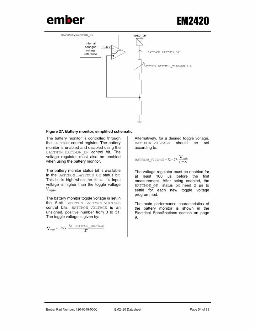
EM2420
Ember Part Number: 120-0049-000C EM2420 Datasheet Page 54 of 89
VREG_IN
Internalbandgapvoltage
reference
1.25 V
BATTMON.BATTMON_VOLTAGE[4:0]
BATTMON.BATTMON_OK
BATTMON.BATTMON_EN
Figure 27. Battery monitor, simplified schematic
The battery monitor is controlled through the BATTMON control register. The battery monitor is enabled and disabled using the BATTMON.BATTMON_EN control bit. The voltage regulator must also be enabled when using the battery monitor.
The battery monitor status bit is available in the BATTMON.BATTMON_OK status bit. This bit is high when the VREG_IN input voltage is higher than the toggle voltage Vtoggle.
The battery monitor toggle voltage is set in the 5-bit BATTMON.BATTMON_VOLTAGE control bits. BATTMON_VOLTAGE is an unsigned, positive number from 0 to 31. The toggle voltage is given by:
2772
V25.1Vtoggle
LTAGEBATTMON_VO−⋅=
Alternatively, for a desired toggle voltage, BATTMON_VOLTAGE should be set according to:
V25.12772 Vtoggle⋅−=LTAGEBATTMON_VO
The voltage regulator must be enabled for at least 100 µs before the first measurement. After being enabled, the BATTMON_OK status bit need 2 µs to settle for each new toggle voltage programmed.
The main performance characteristics of the battery monitor is shown in the Electrical Specifications section on page 9.
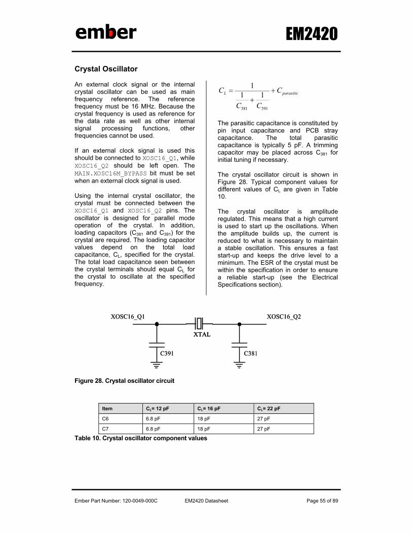
EM2420
Ember Part Number: 120-0049-000C EM2420 Datasheet Page 55 of 89
Crystal Oscillator
An external clock signal or the internal crystal oscillator can be used as main frequency reference. The reference frequency must be 16 MHz. Because the crystal frequency is used as reference for the data rate as well as other internal signal processing functions, other frequencies cannot be used.
If an external clock signal is used this should be connected to XOSC16_Q1, while XOSC16_Q2 should be left open. The MAIN.XOSC16M_BYPASS bit must be set when an external clock signal is used.
Using the internal crystal oscillator, the crystal must be connected between the XOSC16_Q1 and XOSC16_Q2 pins. The oscillator is designed for parallel mode operation of the crystal. In addition, loading capacitors (C381 and C391) for the crystal are required. The loading capacitor values depend on the total load capacitance, CL, specified for the crystal. The total load capacitance seen between the crystal terminals should equal CL for the crystal to oscillate at the specified frequency.
parasiticL C
CC
C ++
=
391381
111
The parasitic capacitance is constituted by pin input capacitance and PCB stray capacitance. The total parasitic capacitance is typically 5 pF. A trimming capacitor may be placed across C381 for initial tuning if necessary.
The crystal oscillator circuit is shown in Figure 28. Typical component values for different values of CL are given in Table 10.
The crystal oscillator is amplitude regulated. This means that a high current is used to start up the oscillations. When the amplitude builds up, the current is reduced to what is necessary to maintain a stable oscillation. This ensures a fast start-up and keeps the drive level to a minimum. The ESR of the crystal must be within the specification in order to ensure a reliable start-up (see the Electrical Specifications section).
C381C391
XTAL
XOSC16_Q1 XOSC16_Q2
C381C391
XTALXTAL
XOSC16_Q1 XOSC16_Q2
Figure 28. Crystal oscillator circuit
Item CL= 12 pF CL= 16 pF CL= 22 pF
C6 6.8 pF 18 pF 27 pF
C7 6.8 pF 18 pF 27 pF
Table 10. Crystal oscillator component values
EM2420
Ember Part Number: 120-0049-000C EM2420 Datasheet Page 56 of 89
Input / Output Matching
The RF input / output is differential (RF_N and RF_P). In addition there is supply switch output pin (TXRX_SWITCH) that must have an external DC path to RF_N and RF_P.
In RX mode the TXRX_SWITCH pin is at ground and will bias the LNA. In TX mode the TXRX_SWITCH pin is at supply rail voltage and will properly bias the internal PA.
The RF output and DC bias can be done using different topologies. Some are shown in Figure 3 and Figure 4.
Component values are given in Table 2. Using a differential antenna, no balun is required.
If a single ended output is required (for a single ended connector or a single ended antenna), a balun should be used for optimum performance. The balun can be realized using discrete inductors and capacitors, or a LTCC balun can be used.
Transmitter Test Modes
The EM2420 can be set into different transmit test modes for performance evaluation. The test mode descriptions in the following sections require that the chip is first reset, the crystal oscillator is enabled using the SXOSCON command strobe and that the crystal oscillator has stabilized.
Unmodulated carrier
An unmodulated carrier may be transmitted by setting MDMCTRL1.TX_MODE to 2, writing 0x1800 to the DACTST register and issue a STXON command strobe. The transmitter is then enabled while the transmitter I/Q DACs are overridden to static values. An
unmodulated carrier will then be available on the RF output pins.
A plot of the single carrier output spectrum from the EM2420 is shown in Figure 29 below.
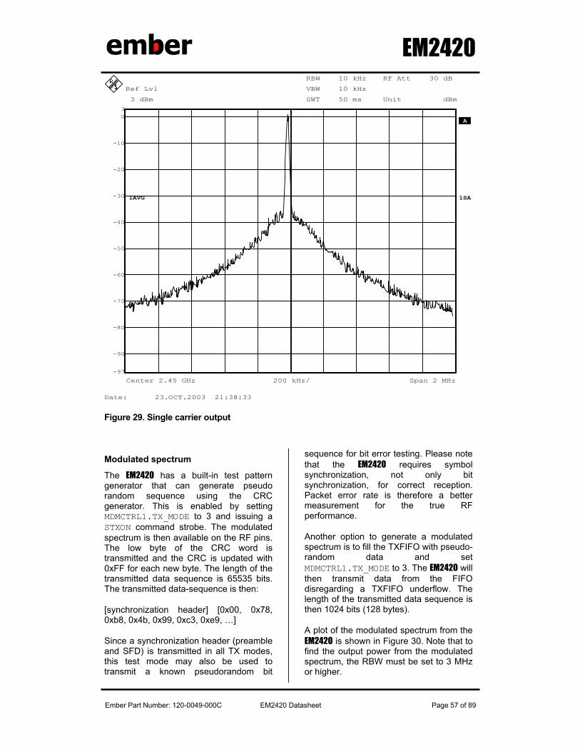
EM2420
Ember Part Number: 120-0049-000C EM2420 Datasheet Page 57 of 89
A
Unit dBm
RF Att 30 dB
1AVG 1SA
Ref Lvl
3 dBm
Ref Lvl
3 dBm
Center 2.45 GHz Span 2 MHz200 kHz/
RBW 10 kHz
VBW 10 kHz
SWT 50 ms
-90
-80
-70
-60
-50
-40
-30
-20
-10
0
-97
3
Date: 23.OCT.2003 21:38:33
Figure 29. Single carrier output
Modulated spectrum
The EM2420 has a built-in test pattern generator that can generate pseudo random sequence using the CRC generator. This is enabled by setting MDMCTRL1.TX_MODE to 3 and issuing a STXON command strobe. The modulated spectrum is then available on the RF pins. The low byte of the CRC word is transmitted and the CRC is updated with 0xFF for each new byte. The length of the transmitted data sequence is 65535 bits. The transmitted data-sequence is then:
[synchronization header] [0x00, 0x78, 0xb8, 0x4b, 0x99, 0xc3, 0xe9, …]
Since a synchronization header (preamble and SFD) is transmitted in all TX modes, this test mode may also be used to transmit a known pseudorandom bit
sequence for bit error testing. Please note that the EM2420 requires symbol synchronization, not only bit synchronization, for correct reception. Packet error rate is therefore a better measurement for the true RF performance.
Another option to generate a modulated spectrum is to fill the TXFIFO with pseudo-random data and set MDMCTRL1.TX_MODE to 3. The EM2420 will then transmit data from the FIFO disregarding a TXFIFO underflow. The length of the transmitted data sequence is then 1024 bits (128 bytes).
A plot of the modulated spectrum from the EM2420 is shown in Figure 30. Note that to find the output power from the modulated spectrum, the RBW must be set to 3 MHz or higher.
EM2420
Ember Part Number: 120-0049-000C EM2420 Datasheet Page 58 of 89
A
Unit dBm
RF Att 30 dB
Ref Lvl
0 dBm
Ref Lvl
0 dBm SWT 5 ms
Center 2.45 GHz Span 10 MHz1 MHz/
1AVG 1SA
RBW 100 kHz
VBW 100 kHz
-90
-80
-70
-60
-50
-40
-30
-20
-10
-100
0
Date: 23.OCT.2003 21:34:19
Figure 30. Modulated spectrum plot
EM2420
Ember Part Number: 120-0049-000C EM2420 Datasheet Page 59 of 89
System Considerations and Guidelines
SRD regulations
International regulations and national laws regulate the use of radio receivers and transmitters. SRDs (Short Range Devices) for license free operation are allowed to operate in the 2.4 GHz band worldwide. The most important regulations are EN 300 440 (Europe), FCC CFR-47 part 15.247 and 15.249 (USA), and ARIB STD- T-66 (Japan).
Frequency hopping and multi-channel systems
The 2.4 GHz band is shared by many systems both in industrial, office and home environments. The EM2420 uses direct sequence spread spectrum (DSSS) as defined by [1] to spread the output power, thereby making the communication link more robust even in a noisy environment.
With the EM2420 it is also possible to combine both DSSS and FHSS (frequency hopping spread spectrum) in a proprietary non-IEEE 802.15.4 system. This is achieved by reprogramming the operating frequency (see the Frequency and Channel Programming section on page 51) before enabling RX or TX. A frequency synchronization scheme must then be implemented within the proprietary MAC layer to make the transmitter and receiver operate on the same RF channel.
Data burst transmissions
The data buffering in the EM2420 lets the user have a lower data rate link between the microcontroller and the RF device than the RF bit rate of 250 kbps. This allows the microcontroller to buffer data at its own speed, reducing the workload and timing requirements.
The relatively high data rate of the EM2420 also reduces the average power consumption compared to the 868 / 915 MHz bands defined by [1], where only 20 / 40 kbps are available. The EM2420 may be powered up a smaller portion of the time, so that the average power consumption is
reduced for a given amount of data to be transferred.
Crystal accuracy and drift
A crystal accuracy of ±40 ppm is required for compliance with IEEE 802.15.4 [1]. This accuracy must also take ageing and temperature drift into consideration.
A crystal with low temperature drift and low aging could be used without further compensation. A trimmer capacitor in the crystal oscillator circuit (in parallel with C7) could be used to set the initial frequency accurately.
For non-IEEE 802.15.4 systems, the robust demodulator in the EM2420 allows up to 120 ppm total frequency offset between the transmitter and receiver. This could e.g. relax the accuracy requirement to 60 ppm for each of the devices.
Optionally in a star network topology, the FFD could be equipped with a more accurate crystal thereby relaxing the requirement on the RFD. This can make sense in systems where the RFDs ship in higher volumes than the FFDs.
Communication robustness
The EM2420 provides very good adjacent, alternate and co channel rejection, image frequency suppression and blocking properties. The EM2420 performance is significantly better than the requirements imposed by [1]. These are highly important parameters for reliable operation in the 2.4 GHz band, since an increasing number of devices/systems are using this license free frequency band.
Communication security
The hardware encryption and authentication operations in the EM2420 enable secure communication, which is required for many applications. Security operations require a lot of data processing which is costly in an 8-bit microcontroller system. The hardware support within the
EM2420
Ember Part Number: 120-0049-000C EM2420 Datasheet Page 60 of 89
EM2420 enables a high level of security even with a low-cost 8 bit controller.
Low cost systems
As the EM2420 provides 250 kbps multi-channel performance without any external filters, a very low cost system can be made.
A differential antenna will eliminate the need for a balun, and the DC biasing can be achieved in the antenna topology.
Battery operated systems
In low power applications, the EM2420 should be powered down when not being active. Extremely low power consumption may be achieved when disabling also the voltage regulator. This will require reprogramming of the register and RAM configuration.
BER / PER measurements
The EM2420 includes test modes where data is received infinitely and output to pins (RX_MODE 2, see page 38). This mode may be used for Bit Error Rate (BER) measurements. However, the following actions must be taken to do such a measurement:
• A preamble and SFD sequence must be used, even if pseudo random data is transmitted, since receiving the DSSS modulated signal requires symbol synchronization, not bit synchronization like e.g. in 2FSK systems. The SYNCWORD may be set to another value to fit to the measurement setup if necessary.
• The data transmitted over air must be spread according to [1] and the description on page 22. This means that the transmitter used during measurements must be able to do spreading of the bit data to chip data. Remember that the chip sequence transmitted by the test setup is not the same as the bit sequence which is output by the EM2420.
• When operating at or below the sensitivity limit, the EM2420 may lose symbol synchronization in infinite receive mode. A new SFD and restart of the receiver may be required to re-gain synchronization.
In an IEEE 802.15.4 system, all communication is based on packets. The sensitivity limit specified by [1] is based on Packet Error Rate (PER) measurements instead of BER. This is a more accurate measurement of the true RF performance since it mirrors the way the actual system operates.
Ember recommends performing PER measurements instead of BER measurements to evaluate the performance of IEEE 802.15.4 systems. To do PER measurements, the following may be used as a guideline:
• A valid preamble, SFD and length field must be used for each packet.
• The PSDU (see Figure 15 on page 34) length should be 20 bytes for sensitivity measurements as specified by [1].
• The sensitivity limit specified by [1] is the RF level resulting in a 1% PER. The packet sample space for a given measurement must then be >> 100 to have a sufficiently large sample space. E.g. at least 1000 packets should be used to measure the sensitivity.
• The data transmitted over air must be spread according to [1] and the description on page 22. Pre-generated packets may be used, although [1] requires that the PER is averaged over random PSDU data.
• The EM2420 receive FIFO may be used to buffer data received during PER measurements, since it is able to buffer up to 128 bytes.
• The MDMCTRL1.CORR_THR control register should be set to
EM2420
Ember Part Number: 120-0049-000C EM2420 Datasheet Page 61 of 89
20, as described in the Demodulator, Symbol Synchronizer and Data Decision section.
The simplest way of making a PER measurement will be to use another EM2420 as the reference transmitter. However, this makes it difficult to measure the exact receiver performance.
Using a signal generator, this may either be set up as O-QPSK with half-sine shaping or as MSK. If using O-QPSK, the phases must be selected according to [1]. If using MSK, the chip sequence must be
modified such that the modulated MSK signal has the same phase shifts as the O-QPSK sequence previously defined.
For a desired symbol sequence s0, s1, … , sn-1 of length n symbols, the desired chip sequence c0, c1, c2, …, c32n-1 of length 32n is found using table lookup from Table 3 on page 22. It can be seen from comparing the phase shifts of the O-QPSK signal with the frequency of a MSK signal that the MSK chip sequence is generated as:
(c0 xnor c1), (c1 xor c2), (c2 xnor c3), … , (c32n-1 xor c32n) where c32n may be arbitrarily selected.
PCB Layout Recommendations
A four layer PCB is highly recommended. The second layer of the PCB should be the used as a ground plane.
The top layer should be used for signal routing, and the open areas should be filled with metallization connected to ground using several vias.
The area under the chip is used for grounding and must be well connected to the ground plane with several vias.
The ground pins should be connected to ground as close as possible to the package pin using individual vias. The de-coupling capacitors should also be placed as close as possible to the supply pins and connected to the ground plane by
separate vias. Supply power filtering is very important.
The external components should be as small as possible (0402 is recommended) and surface mount devices must be used.
Caution should be used when placing the microcontroller in order to avoid interference with the RF circuitry.
A Development Kit with a fully assembled Evaluation Module is available. It is strongly advised that this reference layout is followed very closely in order to get the best performance.
The schematic, BOM and layout Gerber files for the reference designs are all available from the Ember website.
Antenna Considerations
The EM2420 can be used together with various types of antennas. A differential antenna like a dipole would be the easiest to interface not needing a balun (balanced to un-balanced transformation network).
The length of the λ/2-dipole antenna is given by:
L = 14250 / f
where f is in MHz, giving the length in cm. An antenna for 2450 MHz should be 5.8 cm. Each arm is therefore 2.9 cm.
Other commonly used antennas for short-range communication are monopole, helical and loop antennas. The single-ended monopole and helical would require a balun network between the differential output and the antenna.
EM2420
Ember Part Number: 120-0049-000C EM2420 Datasheet Page 62 of 89
Monopole antennas are resonant antennas with a length corresponding to one quarter of the electrical wavelength (λ/4). They are very easy to design and can be implemented simply as a “piece of wire” or even integrated into the PCB.
The length of the λ/4-monopole antenna is given by:
L = 7125 / f
where f is in MHz, giving the length in cm. An antenna for 2450 MHz should be 2.9 cm.
Non-resonant monopole antennas shorter than λ/4 can also be used, but at the expense of range. In size and cost critical applications such an antenna may very well be integrated into the PCB.
Enclosing the antenna in high dielectric constant material reduces the overall size
of the antenna. Many vendors offer such antennas intended for PCB mounting.
Helical antennas can be thought of as a combination of a monopole and a loop antenna. They are a good compromise in size critical applications. Helical antennas tend to be more difficult to optimize than the simple monopole.
Loop antennas are easy to integrate into the PCB, but are less effective due to difficult impedance matching because of their very low radiation resistance.
For low power applications the differential antenna is recommended giving the best range and because of its simplicity.
The antenna should be connected as close as possible to the IC. If the antenna is located away from the RF pins the antenna should be matched to the feeding transmission line (50 Ω).
EM2420
Ember Part Number: 120-0049-000C EM2420 Datasheet Page 63 of 89
Configuration Registers
The configuration of the EM2420 is done by programming the 16-bit configuration registers. Complete descriptions of the registers are given in the following tables. After chip reset (from the RESETn pin or programmable through the MAIN.RESETn configuration bit), all the registers have default values as shown in the tables.
Note that the MAIN register is only reset by using the pin reset RESETn. When writing to this register, all bits will get the value written, not the default value. This also means that the MAIN.RESETn bit must be written both low and then high to perform a chip reset through the serial interface.
15 registers are Strobe Command Registers, listed first in Table 11 below. Accessing these registers will initiate the change of an internal state or mode. There are 33 normal 16-bits registers, also listed
in Table 11. Many of these registers are for test purposes only, and need not be accessed for normal operation of the EM2420.
The FIFOs are accessed through two 8-bit registers, TXFIFO and RXFIFO. The TXFIFO register is write only. Data may still be read out of the TXFIFO through regular RAM access (see section RAM access section on page 27), but data is then not removed from the FIFO. Note that the crystal oscillator must be active for all FIFO and RAM access.
During the address transfer and while writing to the TXFIFO, a status byte is returned on the serial data output pin SO. This status byte is described in Table 5 on page 27.
All configuration and status registers are described in the tables following Table 11.
Address Register Register type Description
0x00 SNOP S No Operation (has no other effect than reading out status-bits)
0x01 SXOSCON S Turn on the crystal oscillator (set XOSC16M_PD = 0 and BIAS_PD = 0)
0x02 STXCAL S Enable and calibrate frequency synthesizer for TX; go from RX / TX to a wait state where only the synthesizer is running.
0x03 SRXON S Enable RX
0x04 STXON S Enable TX after calibration (if not already performed) Start TX in-line encryption if SPI_SEC_MODE ≠ 0
0x05 STXONCCA S If CCA indicates a clear channel: Enable calibration, then TX. Start in-line encryption if SPI_SEC_MODE ≠ 0 else do nothing
0x06 SRFOFF S Disable RX/TX and frequency synthesizer
0x07 SXOSCOFF S Turn off the crystal oscillator and RF
0x08 SFLUSHRX S Flush the RX FIFO buffer and reset the demodulator. Always read at least one byte from the RXFIFO before issuing the SFLUSHRX command strobe
0x09 SFLUSHTX S Flush the TX FIFO buffer
0x0A SACK S Send acknowledge frame, with pending field cleared.
0x0B SACKPEND S Send acknowledge frame, with pending field set.
0x0C SRXDEC S Start RXFIFO in-line decryption / authentication (as set by SPI_SEC_MODE)
0x0D STXENC S Start TXFIFO in-line encryption / authentication (as set by SPI_SEC_MODE), without starting TX.
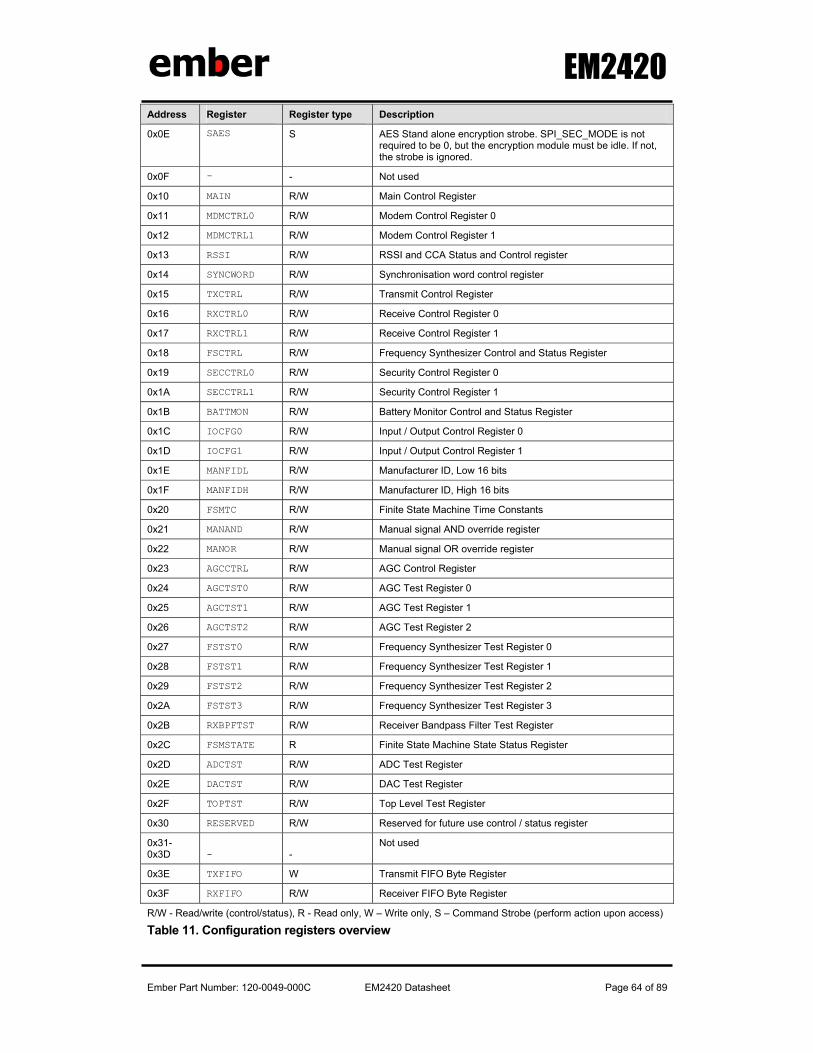
EM2420
Ember Part Number: 120-0049-000C EM2420 Datasheet Page 64 of 89
Address Register Register type Description
0x0E SAES S AES Stand alone encryption strobe. SPI_SEC_MODE is not required to be 0, but the encryption module must be idle. If not, the strobe is ignored.
0x0F - - Not used
0x10 MAIN R/W Main Control Register
0x11 MDMCTRL0 R/W Modem Control Register 0
0x12 MDMCTRL1 R/W Modem Control Register 1
0x13 RSSI R/W RSSI and CCA Status and Control register
0x14 SYNCWORD R/W Synchronisation word control register
0x15 TXCTRL R/W Transmit Control Register
0x16 RXCTRL0 R/W Receive Control Register 0
0x17 RXCTRL1 R/W Receive Control Register 1
0x18 FSCTRL R/W Frequency Synthesizer Control and Status Register
0x19 SECCTRL0 R/W Security Control Register 0
0x1A SECCTRL1 R/W Security Control Register 1
0x1B BATTMON R/W Battery Monitor Control and Status Register
0x1C IOCFG0 R/W Input / Output Control Register 0
0x1D IOCFG1 R/W Input / Output Control Register 1
0x1E MANFIDL R/W Manufacturer ID, Low 16 bits
0x1F MANFIDH R/W Manufacturer ID, High 16 bits
0x20 FSMTC R/W Finite State Machine Time Constants
0x21 MANAND R/W Manual signal AND override register
0x22 MANOR R/W Manual signal OR override register
0x23 AGCCTRL R/W AGC Control Register
0x24 AGCTST0 R/W AGC Test Register 0
0x25 AGCTST1 R/W AGC Test Register 1
0x26 AGCTST2 R/W AGC Test Register 2
0x27 FSTST0 R/W Frequency Synthesizer Test Register 0
0x28 FSTST1 R/W Frequency Synthesizer Test Register 1
0x29 FSTST2 R/W Frequency Synthesizer Test Register 2
0x2A FSTST3 R/W Frequency Synthesizer Test Register 3
0x2B RXBPFTST R/W Receiver Bandpass Filter Test Register
0x2C FSMSTATE R Finite State Machine State Status Register
0x2D ADCTST R/W ADC Test Register
0x2E DACTST R/W DAC Test Register
0x2F TOPTST R/W Top Level Test Register
0x30 RESERVED R/W Reserved for future use control / status register
0x31-0x3D - -
Not used
0x3E TXFIFO W Transmit FIFO Byte Register
0x3F RXFIFO R/W Receiver FIFO Byte Register
R/W - Read/write (control/status), R - Read only, W – Write only, S – Command Strobe (perform action upon access)
Table 11. Configuration registers overview
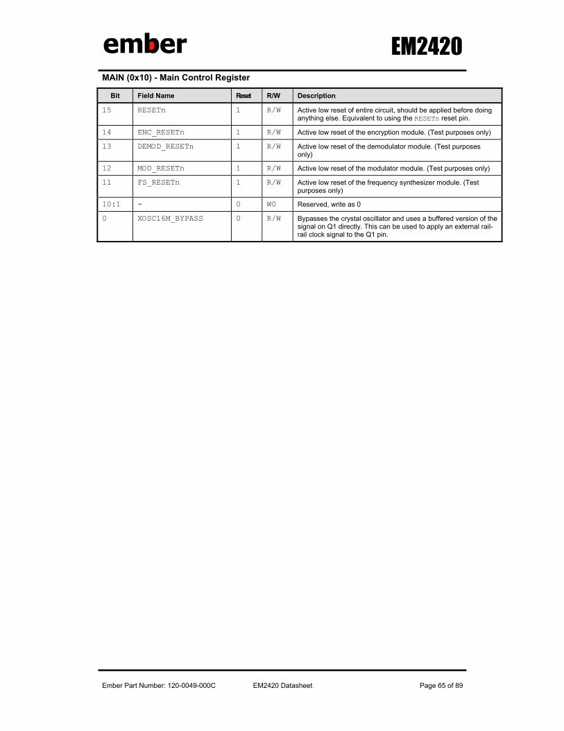
EM2420
Ember Part Number: 120-0049-000C EM2420 Datasheet Page 65 of 89
MAIN (0x10) - Main Control Register
Bit Field Name Reset R/W Description
15 RESETn 1 R/W Active low reset of entire circuit, should be applied before doing anything else. Equivalent to using the RESETn reset pin.
14 ENC_RESETn 1 R/W Active low reset of the encryption module. (Test purposes only)
13 DEMOD_RESETn 1 R/W Active low reset of the demodulator module. (Test purposes only)
12 MOD_RESETn 1 R/W Active low reset of the modulator module. (Test purposes only)
11 FS_RESETn 1 R/W Active low reset of the frequency synthesizer module. (Test purposes only)
10:1 - 0 W0 Reserved, write as 0
0 XOSC16M_BYPASS 0 R/W Bypasses the crystal oscillator and uses a buffered version of the signal on Q1 directly. This can be used to apply an external rail-rail clock signal to the Q1 pin.
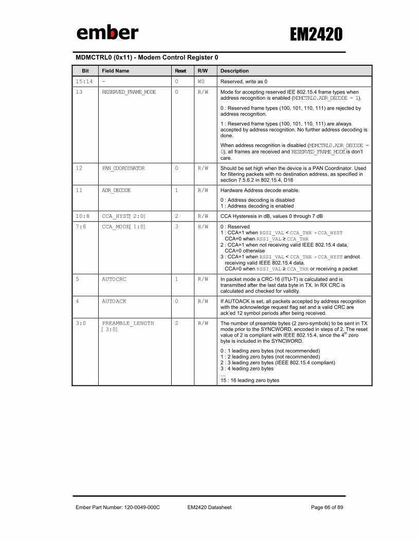
EM2420
Ember Part Number: 120-0049-000C EM2420 Datasheet Page 66 of 89
MDMCTRL0 (0x11) - Modem Control Register 0
Bit Field Name Reset R/W Description
15:14 - 0 W0 Reserved, write as 0
13 RESERVED_FRAME_MODE 0 R/W Mode for accepting reserved IEE 802.15.4 frame types when address recognition is enabled (MDMCTRL0.ADR_DECODE = 1).
0 : Reserved frame types (100, 101, 110, 111) are rejected by address recognition.
1 : Reserved frame types (100, 101, 110, 111) are always accepted by address recognition. No further address decoding is done.
When address recognition is disabled (MDMCTRL0.ADR_DECODE = 0), all frames are received and RESERVED_FRAME_MODE is don’t care.
12 PAN_COORDINATOR 0 R/W Should be set high when the device is a PAN Coordinator. Used for filtering packets with no destination address, as specified in section 7.5.6.2 in 802.15.4, D18
11 ADR_DECODE 1 R/W Hardware Address decode enable.
0 : Address decoding is disabled 1 : Address decoding is enabled
10:8 CCA_HYST[2:0] 2 R/W CCA Hysteresis in dB, values 0 through 7 dB
7:6 CCA_MODE[1:0] 3 R/W 0 : Reserved 1 : CCA=1 when RSSI_VAL < CCA_THR - CCA_HYST CCA=0 when RSSI_VAL ≥ CCA_THR 2 : CCA=1 when not receiving valid IEEE 802.15.4 data, CCA=0 otherwise 3 : CCA=1 when RSSI_VAL < CCA_THR - CCA_HYST andnot receiving valid IEEE 802.15.4 data. CCA=0 when RSSI_VAL ≥ CCA_THR or receiving a packet
5 AUTOCRC 1 R/W In packet mode a CRC-16 (ITU-T) is calculated and is transmitted after the last data byte in TX. In RX CRC is calculated and checked for validity.
4 AUTOACK 0 R/W If AUTOACK is set, all packets accepted by address recognition with the acknowledge request flag set and a valid CRC are ack’ed 12 symbol periods after being received.
3:0 PREAMBLE_LENGTH [3:0]
2 R/W The number of preamble bytes (2 zero-symbols) to be sent in TX mode prior to the SYNCWORD, encoded in steps of 2. The reset value of 2 is compliant with IEEE 802.15.4, since the 4th zero byte is included in the SYNCWORD.
0 : 1 leading zero bytes (not recommended) 1 : 2 leading zero bytes (not recommended) 2 : 3 leading zero bytes (IEEE 802.15.4 compliant) 3 : 4 leading zero bytes … 15 : 16 leading zero bytes
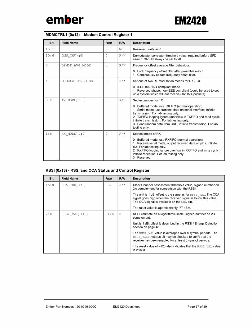
EM2420
Ember Part Number: 120-0049-000C EM2420 Datasheet Page 67 of 89
MDMCTRL1 (0x12) – Modem Control Register 1
Bit Field Name Reset R/W Description
15:11 - 0 W0 Reserved, write as 0.
10:6 CORR_THR[4:0] 0 R/W Demodulator correlator threshold value, required before SFD search. Should always be set to 20.
5 DEMOD_AVG_MODE 0 R/W Frequency offset average filter behaviour.
0 : Lock frequency offset filter after preamble match 1 : Continuously update frequency offset filter.
4 MODULATION_MODE 0 R/W Set one of two RF modulation modes for RX / TX
0 : IEEE 802.15.4 compliant mode 1 : Reversed phase, non-IEEE compliant (could be used to set up a system which will not receive 802.15.4 packets)
3:2 TX_MODE[1:0] 0 R/W Set test modes for TX
0 : Buffered mode, use TXFIFO (normal operation) 1 : Serial mode, use transmit data on serial interface, infinite transmission. For lab testing only. 2 : TXFIFO looping ignore underflow in TXFIFO and read cyclic, infinite transmission. For lab testing only. 3 : Send random data from CRC, infinite transmission. For lab testing only.
1:0 RX_MODE[1:0] 0 R/W Set test mode of RX
0 : Buffered mode, use RXFIFO (normal operation) 1 : Receive serial mode, output received data on pins. Infinite RX. For lab testing only. 2 : RXFIFO looping ignore overflow in RXFIFO and write cyclic, infinite reception. For lab testing only. 3 : Reserved
RSSI (0x13) - RSSI and CCA Status and Control Register
Bit Field Name Reset R/W Description
15:8 CCA_THR[7:0] -32 R/W Clear Channel Assessment threshold value, signed number on 2’s complement for comparison with the RSSI.
The unit is 1 dB; offset is the same as for RSSI_VAL. The CCA signal goes high when the received signal is below this value. The CCA signal is available on the CCA pin.
The reset value is approximately -77 dBm.
7:0 RSSI_VAL[7:0] -128 R RSSI estimate on a logarithmic scale, signed number on 2’s complement.
Unit is 1 dB; offset is described in the RSSI / Energy Detection section on page 48.
The RSSI_VAL value is averaged over 8 symbol periods. The RSSI_VALID status bit may be checked to verify that the receiver has been enabled for at least 8 symbol periods.
The reset value of –128 also indicates that the RSSI_VAL value is invalid.
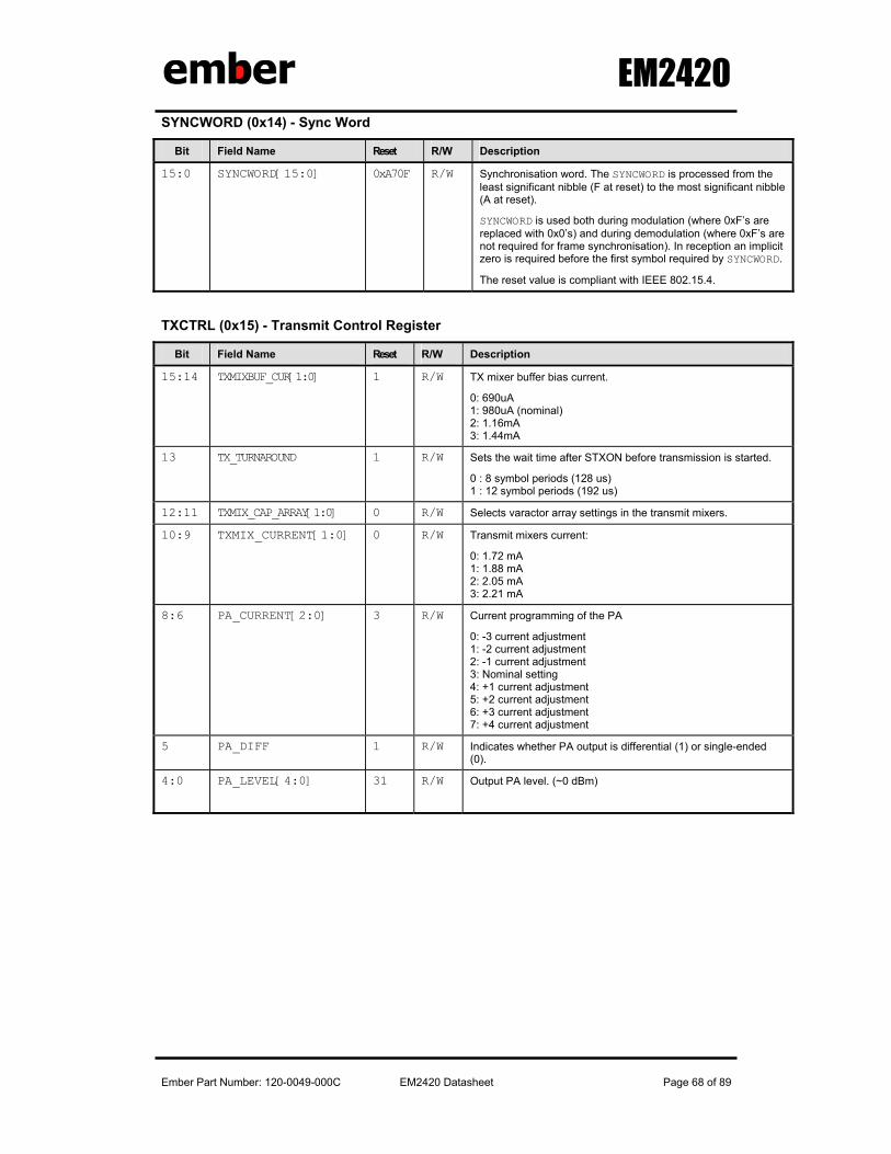
EM2420
Ember Part Number: 120-0049-000C EM2420 Datasheet Page 68 of 89
SYNCWORD (0x14) - Sync Word
Bit Field Name Reset R/W Description
15:0 SYNCWORD[15:0] 0xA70F R/W Synchronisation word. The SYNCWORD is processed from the least significant nibble (F at reset) to the most significant nibble (A at reset).
SYNCWORD is used both during modulation (where 0xF’s are replaced with 0x0’s) and during demodulation (where 0xF’s are not required for frame synchronisation). In reception an implicit zero is required before the first symbol required by SYNCWORD.
The reset value is compliant with IEEE 802.15.4.
TXCTRL (0x15) - Transmit Control Register
Bit Field Name Reset R/W Description
15:14 TXMIXBUF_CUR[1:0] 1 R/W TX mixer buffer bias current.
0: 690uA 1: 980uA (nominal) 2: 1.16mA 3: 1.44mA
13 TX_TURNAROUND 1 R/W Sets the wait time after STXON before transmission is started.
0 : 8 symbol periods (128 us) 1 : 12 symbol periods (192 us)
12:11 TXMIX_CAP_ARRAY[1:0] 0 R/W Selects varactor array settings in the transmit mixers.
10:9 TXMIX_CURRENT[1:0] 0 R/W Transmit mixers current:
0: 1.72 mA 1: 1.88 mA 2: 2.05 mA 3: 2.21 mA
8:6 PA_CURRENT[2:0] 3 R/W Current programming of the PA
0: -3 current adjustment 1: -2 current adjustment 2: -1 current adjustment 3: Nominal setting 4: +1 current adjustment 5: +2 current adjustment 6: +3 current adjustment 7: +4 current adjustment
5 PA_DIFF 1 R/W Indicates whether PA output is differential (1) or single-ended (0).
4:0 PA_LEVEL[4:0] 31 R/W Output PA level. (~0 dBm)
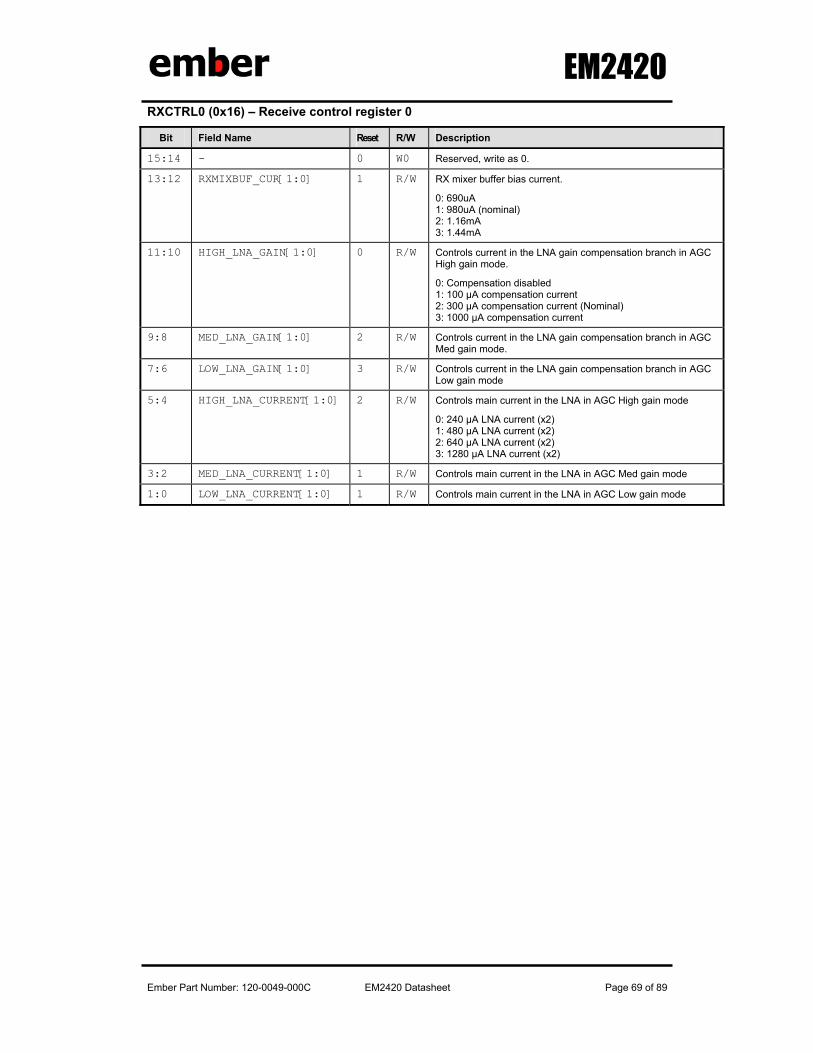
EM2420
Ember Part Number: 120-0049-000C EM2420 Datasheet Page 69 of 89
RXCTRL0 (0x16) – Receive control register 0
Bit Field Name Reset R/W Description
15:14 - 0 W0 Reserved, write as 0.
13:12 RXMIXBUF_CUR[1:0] 1 R/W RX mixer buffer bias current.
0: 690uA 1: 980uA (nominal) 2: 1.16mA 3: 1.44mA
11:10 HIGH_LNA_GAIN[1:0] 0 R/W Controls current in the LNA gain compensation branch in AGC High gain mode.
0: Compensation disabled 1: 100 µA compensation current 2: 300 µA compensation current (Nominal) 3: 1000 µA compensation current
9:8 MED_LNA_GAIN[1:0] 2 R/W Controls current in the LNA gain compensation branch in AGC Med gain mode.
7:6 LOW_LNA_GAIN[1:0] 3 R/W Controls current in the LNA gain compensation branch in AGC Low gain mode
5:4 HIGH_LNA_CURRENT[1:0] 2 R/W Controls main current in the LNA in AGC High gain mode
0: 240 µA LNA current (x2) 1: 480 µA LNA current (x2) 2: 640 µA LNA current (x2) 3: 1280 µA LNA current (x2)
3:2 MED_LNA_CURRENT[1:0] 1 R/W Controls main current in the LNA in AGC Med gain mode
1:0 LOW_LNA_CURRENT[1:0] 1 R/W Controls main current in the LNA in AGC Low gain mode
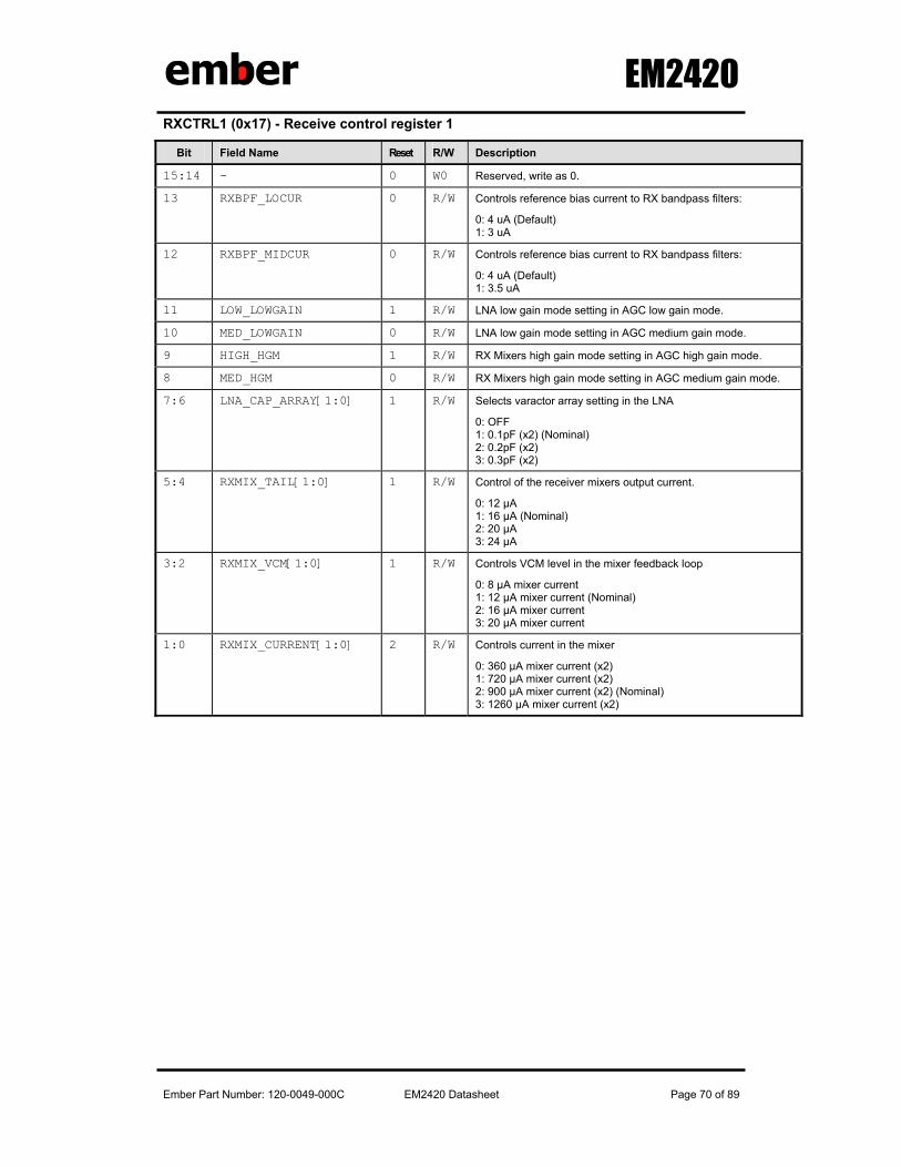
EM2420
Ember Part Number: 120-0049-000C EM2420 Datasheet Page 70 of 89
RXCTRL1 (0x17) - Receive control register 1
Bit Field Name Reset R/W Description
15:14 - 0 W0 Reserved, write as 0.
13 RXBPF_LOCUR 0 R/W Controls reference bias current to RX bandpass filters:
0: 4 uA (Default) 1: 3 uA
12 RXBPF_MIDCUR 0 R/W Controls reference bias current to RX bandpass filters:
0: 4 uA (Default) 1: 3.5 uA
11 LOW_LOWGAIN 1 R/W LNA low gain mode setting in AGC low gain mode.
10 MED_LOWGAIN 0 R/W LNA low gain mode setting in AGC medium gain mode.
9 HIGH_HGM 1 R/W RX Mixers high gain mode setting in AGC high gain mode.
8 MED_HGM 0 R/W RX Mixers high gain mode setting in AGC medium gain mode.
7:6 LNA_CAP_ARRAY[1:0] 1 R/W Selects varactor array setting in the LNA
0: OFF 1: 0.1pF (x2) (Nominal) 2: 0.2pF (x2) 3: 0.3pF (x2)
5:4 RXMIX_TAIL[1:0] 1 R/W Control of the receiver mixers output current.
0: 12 µA 1: 16 µA (Nominal) 2: 20 µA 3: 24 µA
3:2 RXMIX_VCM[1:0] 1 R/W Controls VCM level in the mixer feedback loop
0: 8 µA mixer current 1: 12 µA mixer current (Nominal) 2: 16 µA mixer current 3: 20 µA mixer current
1:0 RXMIX_CURRENT[1:0] 2 R/W Controls current in the mixer
0: 360 µA mixer current (x2) 1: 720 µA mixer current (x2) 2: 900 µA mixer current (x2) (Nominal) 3: 1260 µA mixer current (x2)
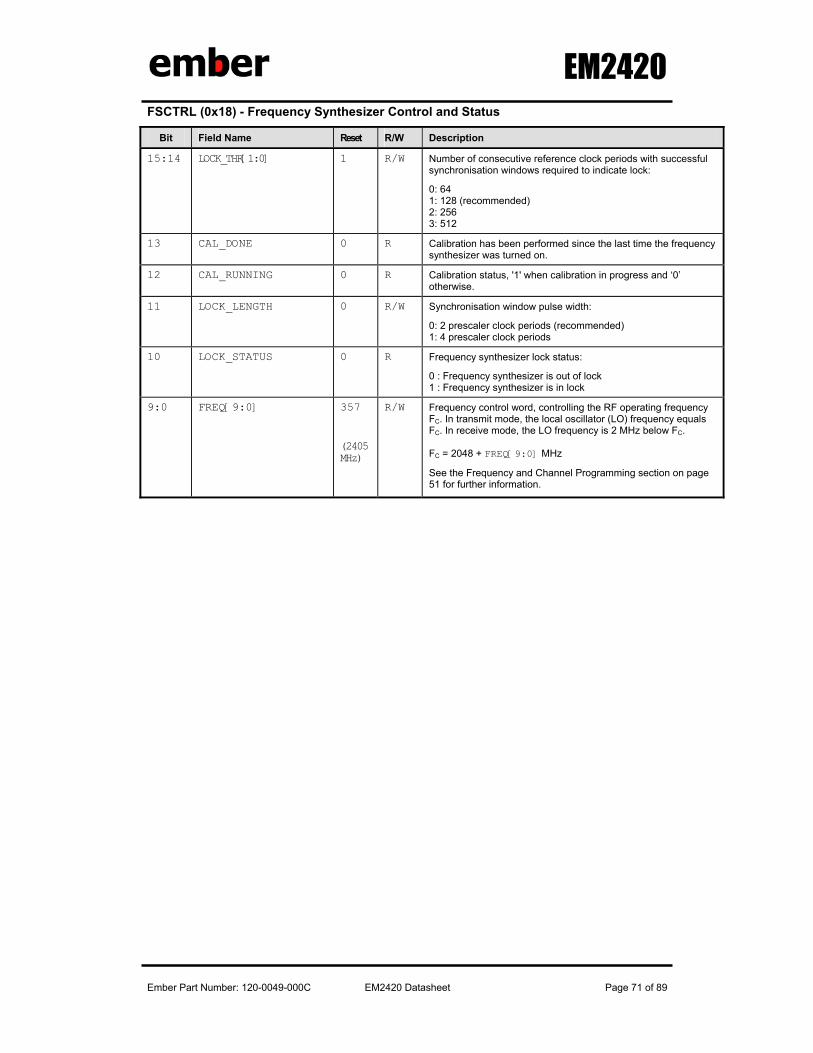
EM2420
Ember Part Number: 120-0049-000C EM2420 Datasheet Page 71 of 89
FSCTRL (0x18) - Frequency Synthesizer Control and Status
Bit Field Name Reset R/W Description
15:14 LOCK_THR[1:0] 1 R/W Number of consecutive reference clock periods with successful synchronisation windows required to indicate lock:
0: 64 1: 128 (recommended) 2: 256 3: 512
13 CAL_DONE 0 R Calibration has been performed since the last time the frequency synthesizer was turned on.
12 CAL_RUNNING 0 R Calibration status, '1' when calibration in progress and ‘0’ otherwise.
11 LOCK_LENGTH 0 R/W Synchronisation window pulse width:
0: 2 prescaler clock periods (recommended) 1: 4 prescaler clock periods
10 LOCK_STATUS 0 R Frequency synthesizer lock status:
0 : Frequency synthesizer is out of lock 1 : Frequency synthesizer is in lock
9:0 FREQ[9:0] 357
(2405 MHz)
R/W Frequency control word, controlling the RF operating frequency FC. In transmit mode, the local oscillator (LO) frequency equals FC. In receive mode, the LO frequency is 2 MHz below FC. FC = 2048 + FREQ[9:0] MHz
See the Frequency and Channel Programming section on page 51 for further information.
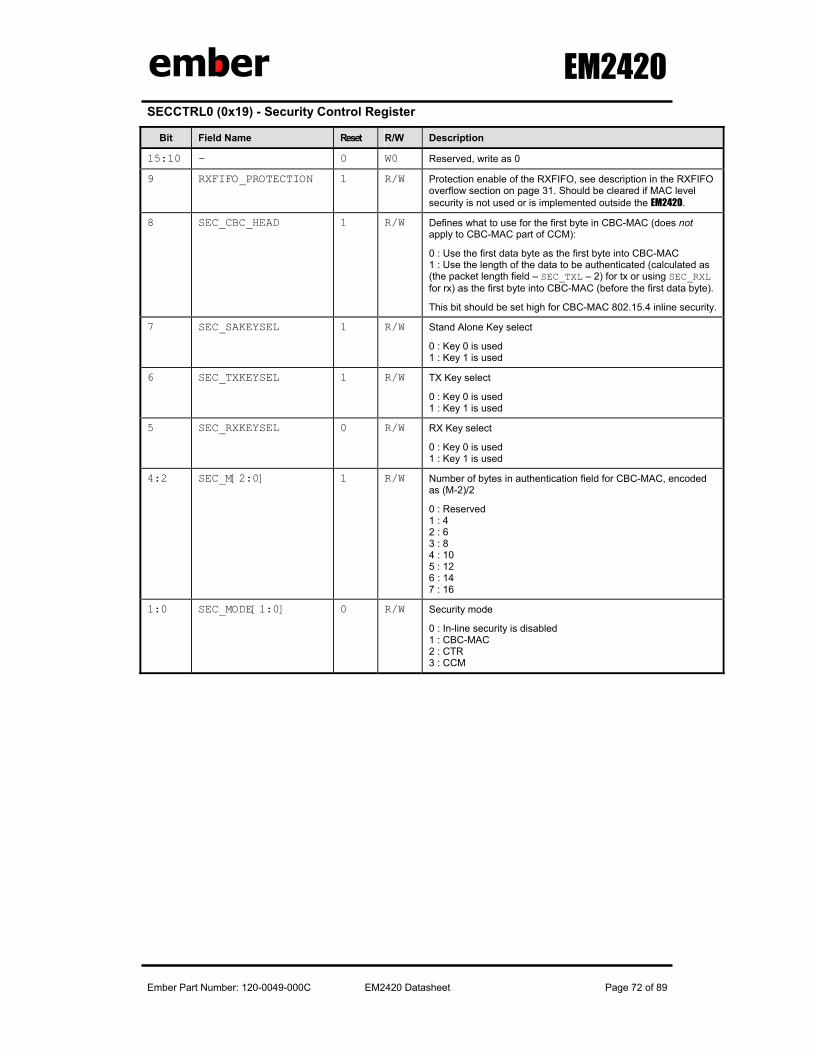
EM2420
Ember Part Number: 120-0049-000C EM2420 Datasheet Page 72 of 89
SECCTRL0 (0x19) - Security Control Register
Bit Field Name Reset R/W Description
15:10 - 0 W0 Reserved, write as 0
9 RXFIFO_PROTECTION 1 R/W Protection enable of the RXFIFO, see description in the RXFIFO overflow section on page 31. Should be cleared if MAC level security is not used or is implemented outside the EM2420.
8 SEC_CBC_HEAD 1 R/W Defines what to use for the first byte in CBC-MAC (does not apply to CBC-MAC part of CCM):
0 : Use the first data byte as the first byte into CBC-MAC 1 : Use the length of the data to be authenticated (calculated as (the packet length field – SEC_TXL – 2) for tx or using SEC_RXL for rx) as the first byte into CBC-MAC (before the first data byte).
This bit should be set high for CBC-MAC 802.15.4 inline security.
7 SEC_SAKEYSEL 1 R/W Stand Alone Key select
0 : Key 0 is used 1 : Key 1 is used
6 SEC_TXKEYSEL 1 R/W TX Key select
0 : Key 0 is used 1 : Key 1 is used
5 SEC_RXKEYSEL 0 R/W RX Key select
0 : Key 0 is used 1 : Key 1 is used
4:2 SEC_M[2:0] 1 R/W Number of bytes in authentication field for CBC-MAC, encoded as (M-2)/2
0 : Reserved 1 : 4 2 : 6 3 : 8 4 : 10 5 : 12 6 : 14 7 : 16
1:0 SEC_MODE[1:0] 0 R/W Security mode
0 : In-line security is disabled 1 : CBC-MAC 2 : CTR 3 : CCM
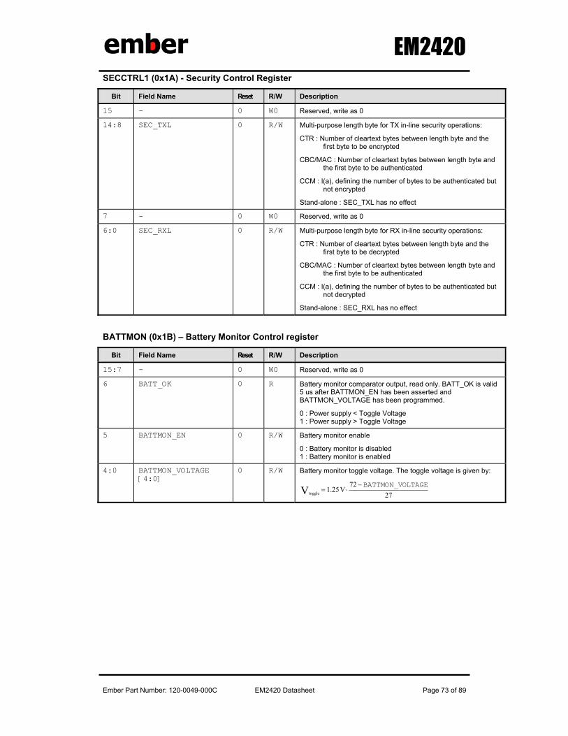
EM2420
Ember Part Number: 120-0049-000C EM2420 Datasheet Page 73 of 89
SECCTRL1 (0x1A) - Security Control Register
Bit Field Name Reset R/W Description
15 - 0 W0 Reserved, write as 0
14:8 SEC_TXL 0 R/W Multi-purpose length byte for TX in-line security operations:
CTR : Number of cleartext bytes between length byte and the first byte to be encrypted
CBC/MAC : Number of cleartext bytes between length byte and the first byte to be authenticated
CCM : l(a), defining the number of bytes to be authenticated but not encrypted
Stand-alone : SEC_TXL has no effect
7 - 0 W0 Reserved, write as 0
6:0 SEC_RXL 0 R/W Multi-purpose length byte for RX in-line security operations:
CTR : Number of cleartext bytes between length byte and the first byte to be decrypted
CBC/MAC : Number of cleartext bytes between length byte and the first byte to be authenticated
CCM : l(a), defining the number of bytes to be authenticated but not decrypted
Stand-alone : SEC_RXL has no effect
BATTMON (0x1B) – Battery Monitor Control register
Bit Field Name Reset R/W Description
15:7 - 0 W0 Reserved, write as 0
6 BATT_OK 0 R Battery monitor comparator output, read only. BATT_OK is valid 5 us after BATTMON_EN has been asserted and BATTMON_VOLTAGE has been programmed.
0 : Power supply < Toggle Voltage 1 : Power supply > Toggle Voltage
5 BATTMON_EN 0 R/W Battery monitor enable
0 : Battery monitor is disabled 1 : Battery monitor is enabled
4:0 BATTMON_VOLTAGE [4:0]
0 R/W Battery monitor toggle voltage. The toggle voltage is given by:
2772
V25.1Vtoggle
LTAGEBATTMON_VO−⋅=
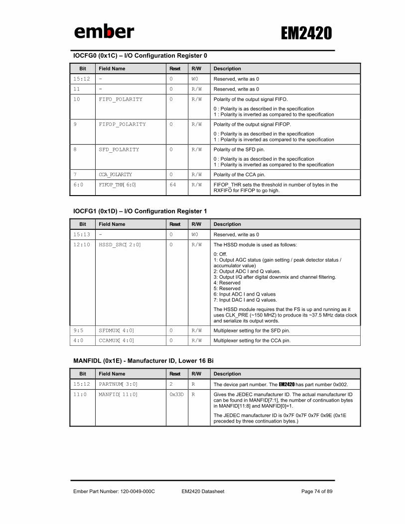
EM2420
Ember Part Number: 120-0049-000C EM2420 Datasheet Page 74 of 89
IOCFG0 (0x1C) – I/O Configuration Register 0
Bit Field Name Reset R/W Description
15:12 - 0 W0 Reserved, write as 0
11 - 0 R/W Reserved, write as 0
10 FIFO_POLARITY 0 R/W Polarity of the output signal FIFO.
0 : Polarity is as described in the specification 1 : Polarity is inverted as compared to the specification
9 FIFOP_POLARITY 0 R/W Polarity of the output signal FIFOP.
0 : Polarity is as described in the specification 1 : Polarity is inverted as compared to the specification
8 SFD_POLARITY 0 R/W Polarity of the SFD pin.
0 : Polarity is as described in the specification 1 : Polarity is inverted as compared to the specification
7 CCA_POLARITY 0 R/W Polarity of the CCA pin.
6:0 FIFOP_THR[6:0] 64 R/W FIFOP_THR sets the threshold in number of bytes in the RXFIFO for FIFOP to go high.
IOCFG1 (0x1D) – I/O Configuration Register 1
Bit Field Name Reset R/W Description
15:13 - 0 W0 Reserved, write as 0
12:10 HSSD_SRC[2:0] 0 R/W The HSSD module is used as follows:
0: Off. 1: Output AGC status (gain setting / peak detector status / accumulator value) 2: Output ADC I and Q values. 3: Output I/Q after digital downmix and channel filtering. 4: Reserved 5: Reserved 6: Input ADC I and Q values 7: Input DAC I and Q values.
The HSSD module requires that the FS is up and running as it uses CLK_PRE (~150 MHZ) to produce its ~37.5 MHz data clock and serialize its output words.
9:5 SFDMUX[4:0] 0 R/W Multiplexer setting for the SFD pin.
4:0 CCAMUX[4:0] 0 R/W Multiplexer setting for the CCA pin.
MANFIDL (0x1E) - Manufacturer ID, Lower 16 Bi
Bit Field Name Reset R/W Description
15:12 PARTNUM[3:0] 2 R The device part number. The EM2420 has part number 0x002.
11:0 MANFID[11:0] 0x33D R Gives the JEDEC manufacturer ID. The actual manufacturer ID can be found in MANFID[7:1], the number of continuation bytes in MANFID[11:8] and MANFID[0]=1.
The JEDEC manufacturer ID is 0x7F 0x7F 0x7F 0x9E (0x1E preceded by three continuation bytes.)
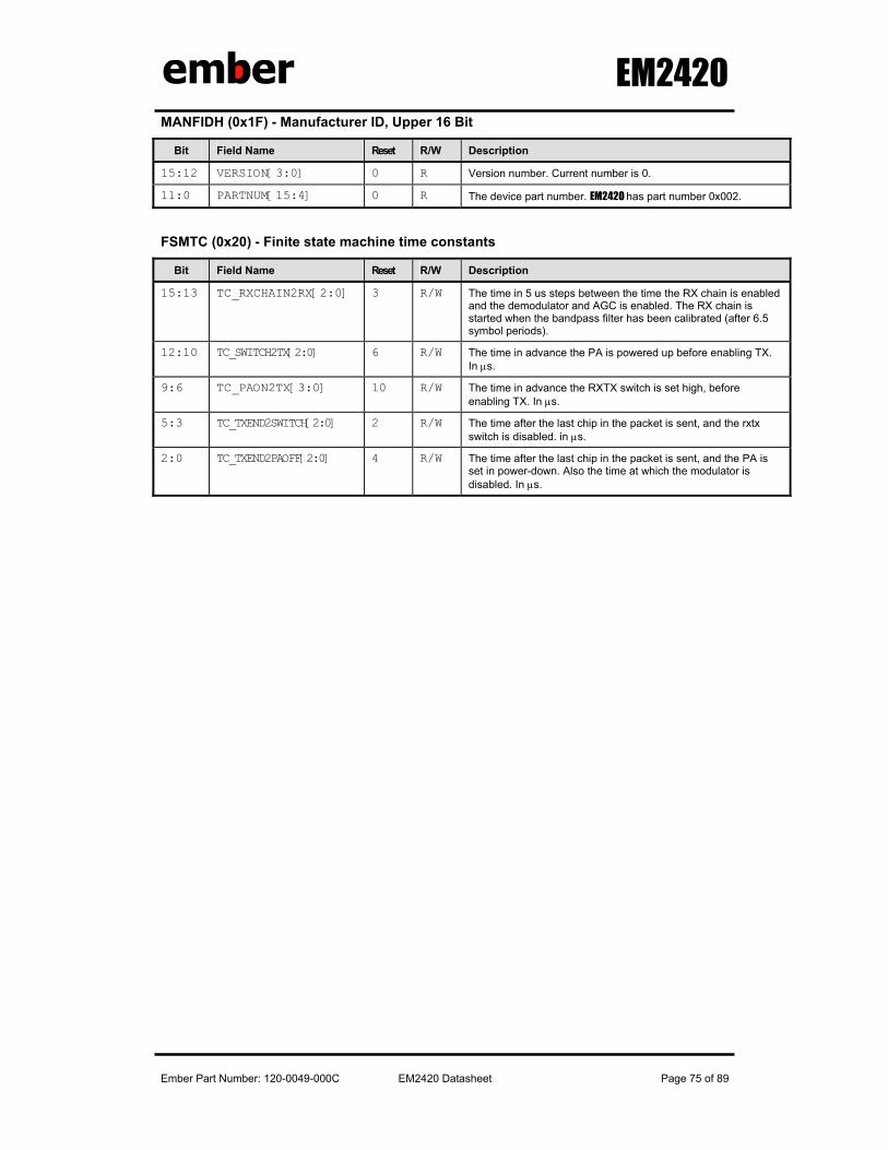
EM2420
Ember Part Number: 120-0049-000C EM2420 Datasheet Page 75 of 89
MANFIDH (0x1F) - Manufacturer ID, Upper 16 Bit
Bit Field Name Reset R/W Description
15:12 VERSION[3:0] 0 R Version number. Current number is 0.
11:0 PARTNUM[15:4] 0 R The device part number. EM2420 has part number 0x002.
FSMTC (0x20) - Finite state machine time constants
Bit Field Name Reset R/W Description
15:13 TC_RXCHAIN2RX[2:0] 3 R/W The time in 5 us steps between the time the RX chain is enabled and the demodulator and AGC is enabled. The RX chain is started when the bandpass filter has been calibrated (after 6.5 symbol periods).
12:10 TC_SWITCH2TX[2:0] 6 R/W The time in advance the PA is powered up before enabling TX. In µs.
9:6 TC_PAON2TX[3:0] 10 R/W The time in advance the RXTX switch is set high, before enabling TX. In µs.
5:3 TC_TXEND2SWITCH[2:0] 2 R/W The time after the last chip in the packet is sent, and the rxtx switch is disabled. in µs.
2:0 TC_TXEND2PAOFF[2:0] 4 R/W The time after the last chip in the packet is sent, and the PA is set in power-down. Also the time at which the modulator is disabled. In µs.
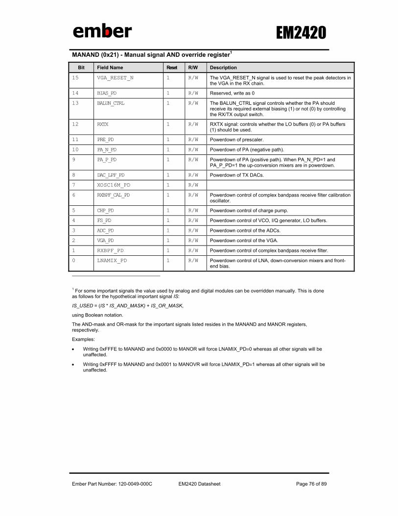
EM2420
Ember Part Number: 120-0049-000C EM2420 Datasheet Page 76 of 89
MANAND (0x21) - Manual signal AND override register1
Bit Field Name Reset R/W Description
15 VGA_RESET_N 1 R/W The VGA_RESET_N signal is used to reset the peak detectors in the VGA in the RX chain.
14 BIAS_PD 1 R/W Reserved, write as 0
13 BALUN_CTRL 1 R/W The BALUN_CTRL signal controls whether the PA should receive its required external biasing (1) or not (0) by controlling the RX/TX output switch.
12 RXTX 1 R/W RXTX signal: controls whether the LO buffers (0) or PA buffers (1) should be used.
11 PRE_PD 1 R/W Powerdown of prescaler.
10 PA_N_PD 1 R/W Powerdown of PA (negative path).
9 PA_P_PD 1 R/W Powerdown of PA (positive path). When PA_N_PD=1 and PA_P_PD=1 the up-conversion mixers are in powerdown.
8 DAC_LPF_PD 1 R/W Powerdown of TX DACs.
7 XOSC16M_PD 1 R/W
6 RXBPF_CAL_PD 1 R/W Powerdown control of complex bandpass receive filter calibration oscillator.
5 CHP_PD 1 R/W Powerdown control of charge pump.
4 FS_PD 1 R/W Powerdown control of VCO, I/Q generator, LO buffers.
3 ADC_PD 1 R/W Powerdown control of the ADCs.
2 VGA_PD 1 R/W Powerdown control of the VGA.
1 RXBPF_PD 1 R/W Powerdown control of complex bandpass receive filter.
0 LNAMIX_PD 1 R/W Powerdown control of LNA, down-conversion mixers and front-end bias.
1 For some important signals the value used by analog and digital modules can be overridden manually. This is done as follows for the hypothetical important signal IS:
IS_USED = (IS * IS_AND_MASK) + IS_OR_MASK,
using Boolean notation.
The AND-mask and OR-mask for the important signals listed resides in the MANAND and MANOR registers, respectively.
Examples:
• Writing 0xFFFE to MANAND and 0x0000 to MANOR will force LNAMIX_PD≡0 whereas all other signals will be unaffected.
• Writing 0xFFFF to MANAND and 0x0001 to MANOVR will force LNAMIX_PD≡1 whereas all other signals will be unaffected.
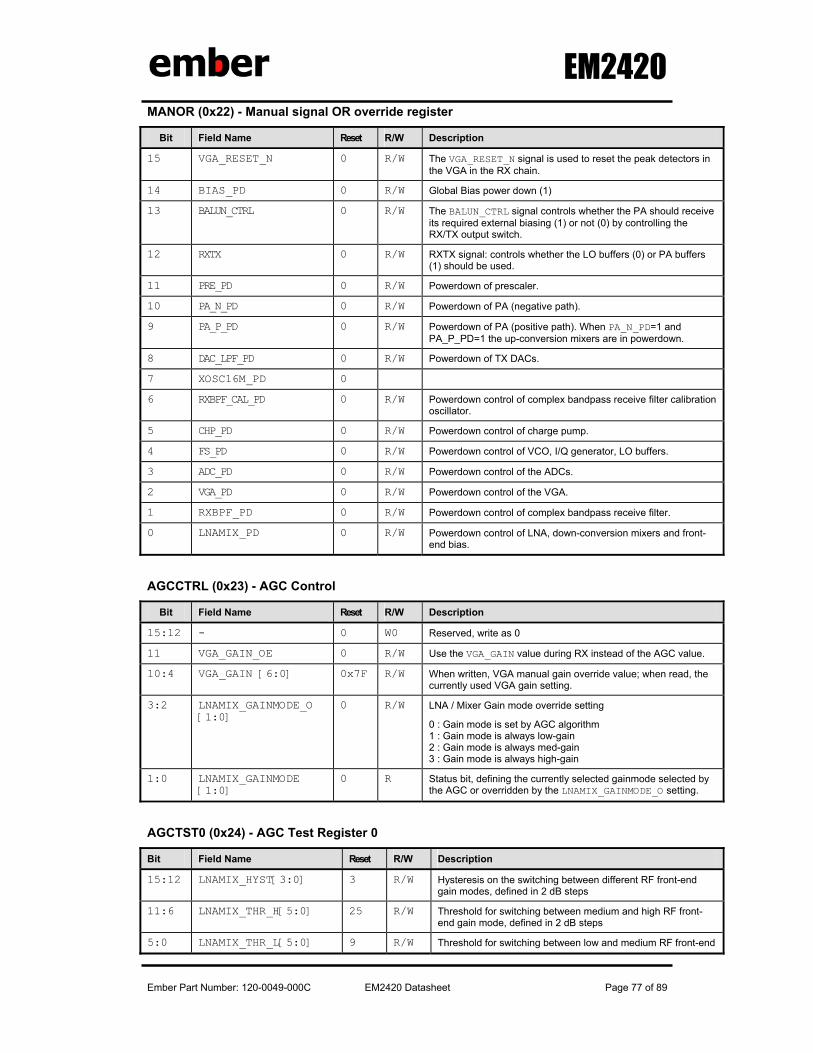
EM2420
Ember Part Number: 120-0049-000C EM2420 Datasheet Page 77 of 89
MANOR (0x22) - Manual signal OR override register
Bit Field Name Reset R/W Description
15 VGA_RESET_N 0 R/W The VGA_RESET_N signal is used to reset the peak detectors in the VGA in the RX chain.
14 BIAS_PD 0 R/W Global Bias power down (1)
13 BALUN_CTRL 0 R/W The BALUN_CTRL signal controls whether the PA should receive its required external biasing (1) or not (0) by controlling the RX/TX output switch.
12 RXTX 0 R/W RXTX signal: controls whether the LO buffers (0) or PA buffers (1) should be used.
11 PRE_PD 0 R/W Powerdown of prescaler.
10 PA_N_PD 0 R/W Powerdown of PA (negative path).
9 PA_P_PD 0 R/W Powerdown of PA (positive path). When PA_N_PD=1 and PA_P_PD=1 the up-conversion mixers are in powerdown.
8 DAC_LPF_PD 0 R/W Powerdown of TX DACs.
7 XOSC16M_PD 0
6 RXBPF_CAL_PD 0 R/W Powerdown control of complex bandpass receive filter calibration oscillator.
5 CHP_PD 0 R/W Powerdown control of charge pump.
4 FS_PD 0 R/W Powerdown control of VCO, I/Q generator, LO buffers.
3 ADC_PD 0 R/W Powerdown control of the ADCs.
2 VGA_PD 0 R/W Powerdown control of the VGA.
1 RXBPF_PD 0 R/W Powerdown control of complex bandpass receive filter.
0 LNAMIX_PD 0 R/W Powerdown control of LNA, down-conversion mixers and front-end bias.
AGCCTRL (0x23) - AGC Control
Bit Field Name Reset R/W Description
15:12 - 0 W0 Reserved, write as 0
11 VGA_GAIN_OE 0 R/W Use the VGA_GAIN value during RX instead of the AGC value.
10:4 VGA_GAIN [6:0] 0x7F R/W When written, VGA manual gain override value; when read, the currently used VGA gain setting.
3:2 LNAMIX_GAINMODE_O [1:0]
0 R/W LNA / Mixer Gain mode override setting
0 : Gain mode is set by AGC algorithm 1 : Gain mode is always low-gain 2 : Gain mode is always med-gain 3 : Gain mode is always high-gain
1:0 LNAMIX_GAINMODE [1:0]
0 R Status bit, defining the currently selected gainmode selected by the AGC or overridden by the LNAMIX_GAINMODE_O setting.
AGCTST0 (0x24) - AGC Test Register 0
Bit Field Name Reset R/W Description
15:12 LNAMIX_HYST[3:0] 3 R/W Hysteresis on the switching between different RF front-end gain modes, defined in 2 dB steps
11:6 LNAMIX_THR_H[5:0] 25 R/W Threshold for switching between medium and high RF front-end gain mode, defined in 2 dB steps
5:0 LNAMIX_THR_L[5:0] 9 R/W Threshold for switching between low and medium RF front-end
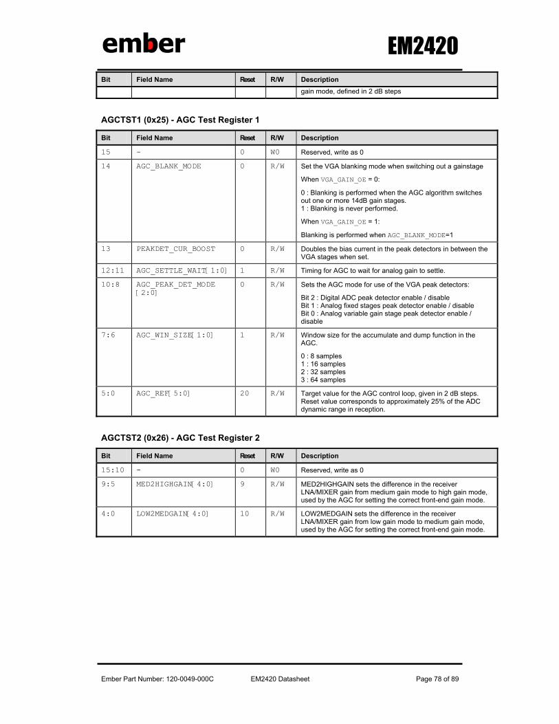
EM2420
Ember Part Number: 120-0049-000C EM2420 Datasheet Page 78 of 89
Bit Field Name Reset R/W Description gain mode, defined in 2 dB steps
AGCTST1 (0x25) - AGC Test Register 1
Bit Field Name Reset R/W Description
15 - 0 W0 Reserved, write as 0
14 AGC_BLANK_MODE 0 R/W Set the VGA blanking mode when switching out a gainstage
When VGA_GAIN_OE = 0:
0 : Blanking is performed when the AGC algorithm switches out one or more 14dB gain stages. 1 : Blanking is never performed.
When VGA_GAIN_OE = 1:
Blanking is performed when AGC_BLANK_MODE=1
13 PEAKDET_CUR_BOOST 0 R/W Doubles the bias current in the peak detectors in between the VGA stages when set.
12:11 AGC_SETTLE_WAIT[1:0] 1 R/W Timing for AGC to wait for analog gain to settle.
10:8 AGC_PEAK_DET_MODE [2:0]
0 R/W Sets the AGC mode for use of the VGA peak detectors:
Bit 2 : Digital ADC peak detector enable / disable Bit 1 : Analog fixed stages peak detector enable / disable Bit 0 : Analog variable gain stage peak detector enable / disable
7:6 AGC_WIN_SIZE[1:0] 1 R/W Window size for the accumulate and dump function in the AGC.
0 : 8 samples 1 : 16 samples 2 : 32 samples 3 : 64 samples
5:0 AGC_REF[5:0] 20 R/W Target value for the AGC control loop, given in 2 dB steps. Reset value corresponds to approximately 25% of the ADC dynamic range in reception.
AGCTST2 (0x26) - AGC Test Register 2
Bit Field Name Reset R/W Description
15:10 - 0 W0 Reserved, write as 0
9:5 MED2HIGHGAIN[4:0] 9 R/W MED2HIGHGAIN sets the difference in the receiver LNA/MIXER gain from medium gain mode to high gain mode, used by the AGC for setting the correct front-end gain mode.
4:0 LOW2MEDGAIN[4:0] 10 R/W LOW2MEDGAIN sets the difference in the receiver LNA/MIXER gain from low gain mode to medium gain mode, used by the AGC for setting the correct front-end gain mode.
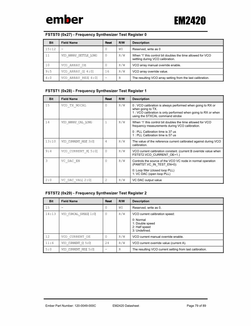
EM2420
Ember Part Number: 120-0049-000C EM2420 Datasheet Page 79 of 89
FSTST0 (0x27) - Frequency Synthesizer Test Register 0
Bit Field Name Reset R/W Description
15:12 - 0 W0 Reserved, write as 0
11 VCO_ARRAY_SETTLE_LONG 0 R/W When '1' this control bit doubles the time allowed for VCO settling during VCO calibration.
10 VCO_ARRAY_OE 0 R/W VCO array manual override enable.
9:5 VCO_ARRAY_O[4:0] 16 R/W VCO array override value.
4:0 VCO_ARRAY_RES[4:0] - R The resulting VCO array setting from the last calibration.
FSTST1 (0x28) - Frequency Synthesizer Test Register 1
Bit Field Name Reset R/W Description
15 VCO_TX_NOCAL 0 R/W 0 : VCO calibration is always performed when going to RX or when going to TX. 1 : VCO calibration is only performed when going to RX or when using the STXCAL command strobe
14 VCO_ARRAY_CAL_LONG 1 R/W When ‘1’ this control bit doubles the time allowed for VCO frequency measurements during VCO calibration.
0 : PLL Calibration time is 37 us 1 : PLL Calibration time is 57 us
13:10 VCO_CURRENT_REF[3:0] 4 R/W The value of the reference current calibrated against during VCO calibration.
9:4 VCO_CURRENT_K[5:0] 0 R/W VCO current calibration constant. (current B override value when FSTST2.VCO_CURRENT_OE=1.)
3 VC_DAC_EN 0 R/W Controls the source of the VCO VC node in normal operation (PAMTST.VC_IN_TEST_EN=0):
0: Loop filter (closed loop PLL) 1: VC DAC (open loop PLL)
2:0 VC_DAC_VAL[2:0] 2 R/W VC DAC output value
FSTST2 (0x29) - Frequency Synthesizer Test Register 2
Bit Field Name Reset R/W Description
15 - 0 W0 Reserved, write as 0.
14:13 VCO_CURCAL_SPEED[1:0] 0 R/W VCO current calibration speed:
0: Normal 1: Double speed 2: Half speed 3: Undefined.
12 VCO_CURRENT_OE 0 R/W VCO current manual override enable.
11:6 VCO_CURRENT_O[5:0] 24 R/W VCO current override value (current A).
5:0 VCO_CURRENT_RES[5:0] - R The resulting VCO current setting from last calibration.
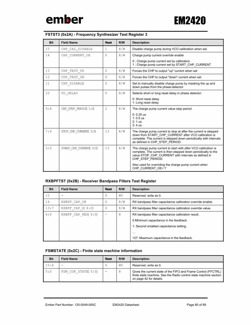
EM2420
Ember Part Number: 120-0049-000C EM2420 Datasheet Page 80 of 89
FSTST3 (0x2A) - Frequency Synthesizer Test Register 3
Bit Field Name Reset R/W Description
15 CHP_CAL_DISABLE 1 R/W Disable charge pump during VCO calibration when set.
14 CHP_CURRENT_OE 0 R/W Charge pump current override enable
0 : Charge pump current set by calibration 1 : Charge pump current set by START_CHP_CURRENT
13 CHP_TEST_UP 0 R/W Forces the CHP to output "up" current when set
12 CHP_TEST_DN 0 R/W Forces the CHP to output "down" current when set
11 CHP_DISABLE 0 R/W Set to manually disable charge pump by masking the up and down pulses from the phase-detector.
10 PD_DELAY 0 R/W Selects short or long reset delay in phase detector:
0: Short reset delay 1: Long reset delay
9:8 CHP_STEP_PERIOD[1:0] 2 R/W The charge pump current value step period:
0: 0.25 us 1: 0.5 us 2: 1 us 3: 4 us
7:4 STOP_CHP_CURRENT[3:0] 13 R/W The charge pump current to stop at after the current is stepped down from START_CHP_CURRENT after VCO calibration is complete. The current is stepped down periodically with intervals as defined in CHP_STEP_PERIOD.
3:0 START_CHP_CURRENT[3:0] 13 R/W The charge pump current to start with after VCO calibration is complete. The current is then stepped down periodically to the value STOP_CHP_CURRENT with intervals as defined in CHP_STEP_PERIOD.
Also used for overriding the charge pump current when CHP_CURRENT_OE=’1’
RXBPFTST (0x2B) - Receiver Bandpass Filters Test Register
Bit Field Name Reset R/W Description
15 - 0 W0 Reserved, write as 0.
14 RXBPF_CAP_OE 0 R/W RX bandpass filter capacitance calibration override enable.
13:7 RXBPF_CAP_O[6:0] 0 R/W RX bandpass filter capacitance calibration override value.
6:0 RXBPF_CAP_RES[6:0] - R RX bandpass filter capacitance calibration result.
0 Minimum capacitance in the feedback.
1: Second smallest capacitance setting.
…
127: Maximum capacitance in the feedback.
FSMSTATE (0x2C) - Finite state machine information
Bit Field Name Reset R/W Description
15:6 - 0 W0 Reserved, write as 0.
5:0 FSM_CUR_STATE[5:0] - R Gives the current state of the FIFO and Frame Control (FFCTRL) finite state machine. See the Radio control state machine section on page 42 for details.
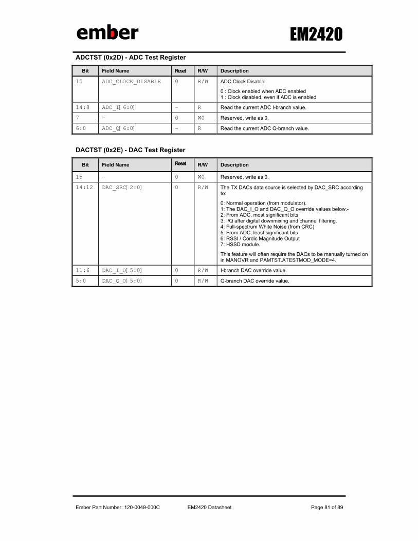
EM2420
Ember Part Number: 120-0049-000C EM2420 Datasheet Page 81 of 89
ADCTST (0x2D) - ADC Test Register
Bit Field Name Reset R/W Description
15 ADC_CLOCK_DISABLE 0 R/W ADC Clock Disable
0 : Clock enabled when ADC enabled 1 : Clock disabled, even if ADC is enabled
14:8 ADC_I[6:0] - R Read the current ADC I-branch value.
7 - 0 W0 Reserved, write as 0.
6:0 ADC_Q[6:0] - R Read the current ADC Q-branch value.
DACTST (0x2E) - DAC Test Register
Bit Field Name Reset R/W Description
15 - 0 W0 Reserved, write as 0.
14:12 DAC_SRC[2:0] 0 R/W The TX DACs data source is selected by DAC_SRC according to:
0: Normal operation (from modulator). 1: The DAC_I_O and DAC_Q_O override values below.- 2: From ADC, most significant bits 3: I/Q after digital downmixing and channel filtering. 4: Full-spectrum White Noise (from CRC) 5: From ADC, least significant bits 6: RSSI / Cordic Magnitude Output 7: HSSD module.
This feature will often require the DACs to be manually turned on in MANOVR and PAMTST.ATESTMOD_MODE=4.
11:6 DAC_I_O[5:0] 0 R/W I-branch DAC override value.
5:0 DAC_Q_O[5:0] 0 R/W Q-branch DAC override value.
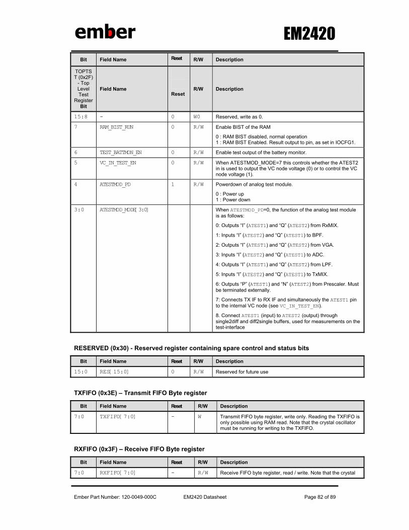
EM2420
Ember Part Number: 120-0049-000C EM2420 Datasheet Page 82 of 89
Bit Field Name Reset R/W Description
TOPTST (0x2F)
- Top Level Test
Register Bit
Field Name
Reset R/W Description
15:8 - 0 W0 Reserved, write as 0.
7 RAM_BIST_RUN 0 R/W Enable BIST of the RAM
0 : RAM BIST disabled, normal operation 1 : RAM BIST Enabled. Result output to pin, as set in IOCFG1.
6 TEST_BATTMON_EN 0 R/W Enable test output of the battery monitor.
5 VC_IN_TEST_EN 0 R/W When ATESTMOD_MODE=7 this controls whether the ATEST2 in is used to output the VC node voltage (0) or to control the VC node voltage (1).
4 ATESTMOD_PD 1 R/W Powerdown of analog test module.
0 : Power up 1 : Power down
3:0 ATESTMOD_MODE[3:0] When ATESTMOD_PD=0, the function of the analog test module is as follows:
0: Outputs “I” (ATEST1) and “Q” (ATEST2) from RxMIX.
1: Inputs “I” (ATEST2) and “Q” (ATEST1) to BPF.
2: Outputs “I” (ATEST1) and “Q” (ATEST2) from VGA.
3: Inputs “I” (ATEST2) and “Q” (ATEST1) to ADC.
4: Outputs “I” (ATEST1) and “Q” (ATEST2) from LPF.
5: Inputs “I” (ATEST2) and “Q” (ATEST1) to TxMIX.
6: Outputs “P” (ATEST1) and “N” (ATEST2) from Prescaler. Must be terminated externally.
7: Connects TX IF to RX IF and simultaneously the ATEST1 pin to the internal VC node (see VC_IN_TEST_EN).
8. Connect ATEST1 (input) to ATEST2 (output) through single2diff and diff2single buffers, used for measurements on the test-interface
RESERVED (0x30) - Reserved register containing spare control and status bits
Bit Field Name Reset R/W Description
15:0 RES[15:0] 0 R/W Reserved for future use
TXFIFO (0x3E) – Transmit FIFO Byte register
Bit Field Name Reset R/W Description
7:0 TXFIFO[7:0] - W Transmit FIFO byte register, write only. Reading the TXFIFO is only possible using RAM read. Note that the crystal oscillator must be running for writing to the TXFIFO.
RXFIFO (0x3F) – Receive FIFO Byte register
Bit Field Name Reset R/W Description
7:0 RXFIFO[7:0] - R/W Receive FIFO byte register, read / write. Note that the crystal
EM2420
Ember Part Number: 120-0049-000C EM2420 Datasheet Page 83 of 89
Bit Field Name Reset R/W Description oscillator must be running for accessing the RXFIFO.
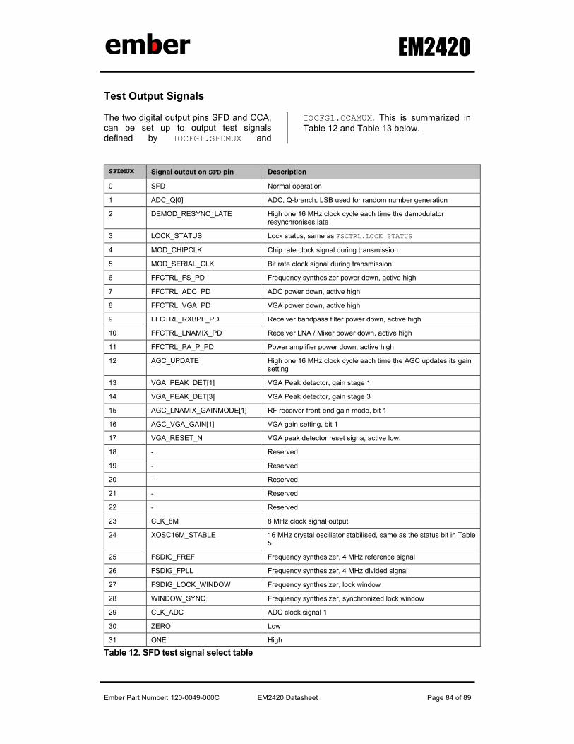
EM2420
Ember Part Number: 120-0049-000C EM2420 Datasheet Page 84 of 89
Test Output Signals
The two digital output pins SFD and CCA, can be set up to output test signals defined by IOCFG1.SFDMUX and
IOCFG1.CCAMUX. This is summarized in Table 12 and Table 13 below.
SFDMUX Signal output on SFD pin Description
0 SFD Normal operation
1 ADC_Q[0] ADC, Q-branch, LSB used for random number generation
2 DEMOD_RESYNC_LATE High one 16 MHz clock cycle each time the demodulator resynchronises late
3 LOCK_STATUS Lock status, same as FSCTRL.LOCK_STATUS
4 MOD_CHIPCLK Chip rate clock signal during transmission
5 MOD_SERIAL_CLK Bit rate clock signal during transmission
6 FFCTRL_FS_PD Frequency synthesizer power down, active high
7 FFCTRL_ADC_PD ADC power down, active high
8 FFCTRL_VGA_PD VGA power down, active high
9 FFCTRL_RXBPF_PD Receiver bandpass filter power down, active high
10 FFCTRL_LNAMIX_PD Receiver LNA / Mixer power down, active high
11 FFCTRL_PA_P_PD Power amplifier power down, active high
12 AGC_UPDATE High one 16 MHz clock cycle each time the AGC updates its gain setting
13 VGA_PEAK_DET[1] VGA Peak detector, gain stage 1
14 VGA_PEAK_DET[3] VGA Peak detector, gain stage 3
15 AGC_LNAMIX_GAINMODE[1] RF receiver front-end gain mode, bit 1
16 AGC_VGA_GAIN[1] VGA gain setting, bit 1
17 VGA_RESET_N VGA peak detector reset signa, active low.
18 - Reserved
19 - Reserved
20 - Reserved
21 - Reserved
22 - Reserved
23 CLK_8M 8 MHz clock signal output
24 XOSC16M_STABLE 16 MHz crystal oscillator stabilised, same as the status bit in Table 5
25 FSDIG_FREF Frequency synthesizer, 4 MHz reference signal
26 FSDIG_FPLL Frequency synthesizer, 4 MHz divided signal
27 FSDIG_LOCK_WINDOW Frequency synthesizer, lock window
28 WINDOW_SYNC Frequency synthesizer, synchronized lock window
29 CLK_ADC ADC clock signal 1
30 ZERO Low
31 ONE High
Table 12. SFD test signal select table
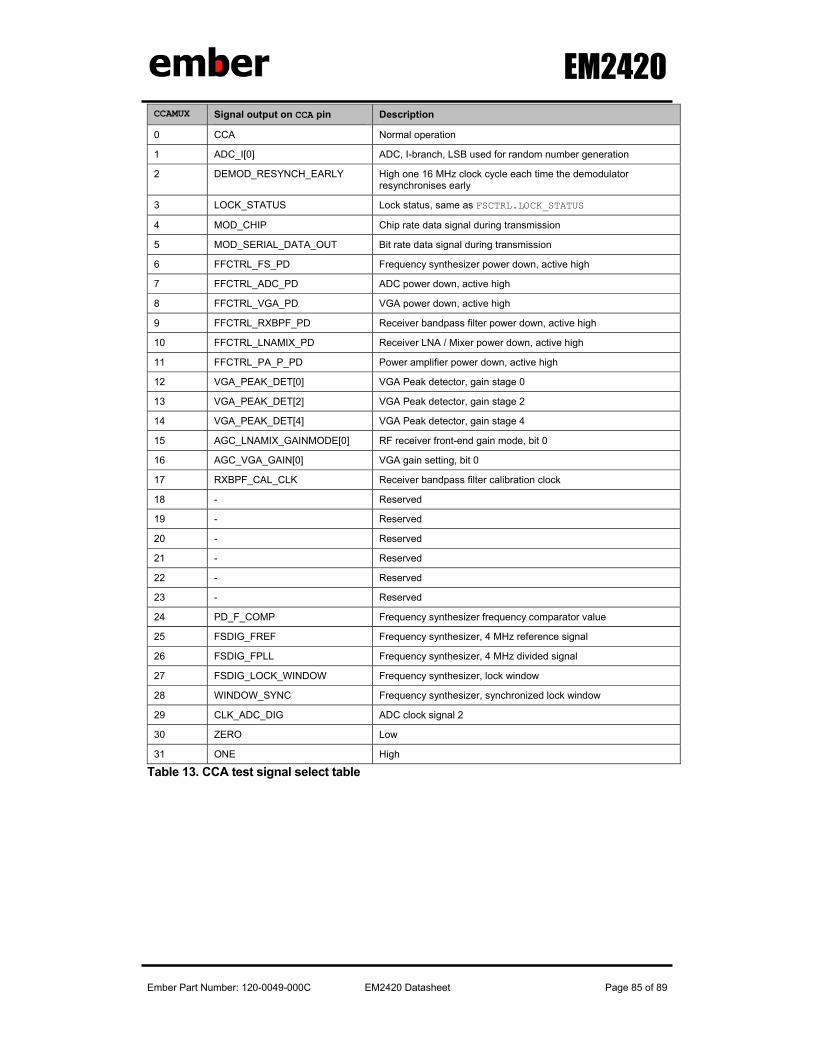
EM2420
Ember Part Number: 120-0049-000C EM2420 Datasheet Page 85 of 89
CCAMUX Signal output on CCA pin Description
0 CCA Normal operation
1 ADC_I[0] ADC, I-branch, LSB used for random number generation
2 DEMOD_RESYNCH_EARLY High one 16 MHz clock cycle each time the demodulator resynchronises early
3 LOCK_STATUS Lock status, same as FSCTRL.LOCK_STATUS
4 MOD_CHIP Chip rate data signal during transmission
5 MOD_SERIAL_DATA_OUT Bit rate data signal during transmission
6 FFCTRL_FS_PD Frequency synthesizer power down, active high
7 FFCTRL_ADC_PD ADC power down, active high
8 FFCTRL_VGA_PD VGA power down, active high
9 FFCTRL_RXBPF_PD Receiver bandpass filter power down, active high
10 FFCTRL_LNAMIX_PD Receiver LNA / Mixer power down, active high
11 FFCTRL_PA_P_PD Power amplifier power down, active high
12 VGA_PEAK_DET[0] VGA Peak detector, gain stage 0
13 VGA_PEAK_DET[2] VGA Peak detector, gain stage 2
14 VGA_PEAK_DET[4] VGA Peak detector, gain stage 4
15 AGC_LNAMIX_GAINMODE[0] RF receiver front-end gain mode, bit 0
16 AGC_VGA_GAIN[0] VGA gain setting, bit 0
17 RXBPF_CAL_CLK Receiver bandpass filter calibration clock
18 - Reserved
19 - Reserved
20 - Reserved
21 - Reserved
22 - Reserved
23 - Reserved
24 PD_F_COMP Frequency synthesizer frequency comparator value
25 FSDIG_FREF Frequency synthesizer, 4 MHz reference signal
26 FSDIG_FPLL Frequency synthesizer, 4 MHz divided signal
27 FSDIG_LOCK_WINDOW Frequency synthesizer, lock window
28 WINDOW_SYNC Frequency synthesizer, synchronized lock window
29 CLK_ADC_DIG ADC clock signal 2
30 ZERO Low
31 ONE High
Table 13. CCA test signal select table

EM2420
Ember Part Number: 120-0049-000C EM2420 Datasheet Page 86 of 89
Package Description (QLP 48)
Note: The figure is an illustration only and not to scale.
Quad Leadless Package (QLP)
D D1 E E1 e b L D2 E2
QLP 48 Min
Max
6.9
7.0
7.1
6.65
6.75
6.85
6.9
7.0
7.1
6.65
6.75
6.85
0.5
0.18
0.30
0.3
0.4
0.5
5.05
5.10
5.15
5.05
5.10
5.15
All dimensions in mm
The package is compliant to JEDEC standard MO-220.
Package thermal properties
Thermal resistance
Air velocity [m/s] 0
Rth,j-a [K/W] 25.6
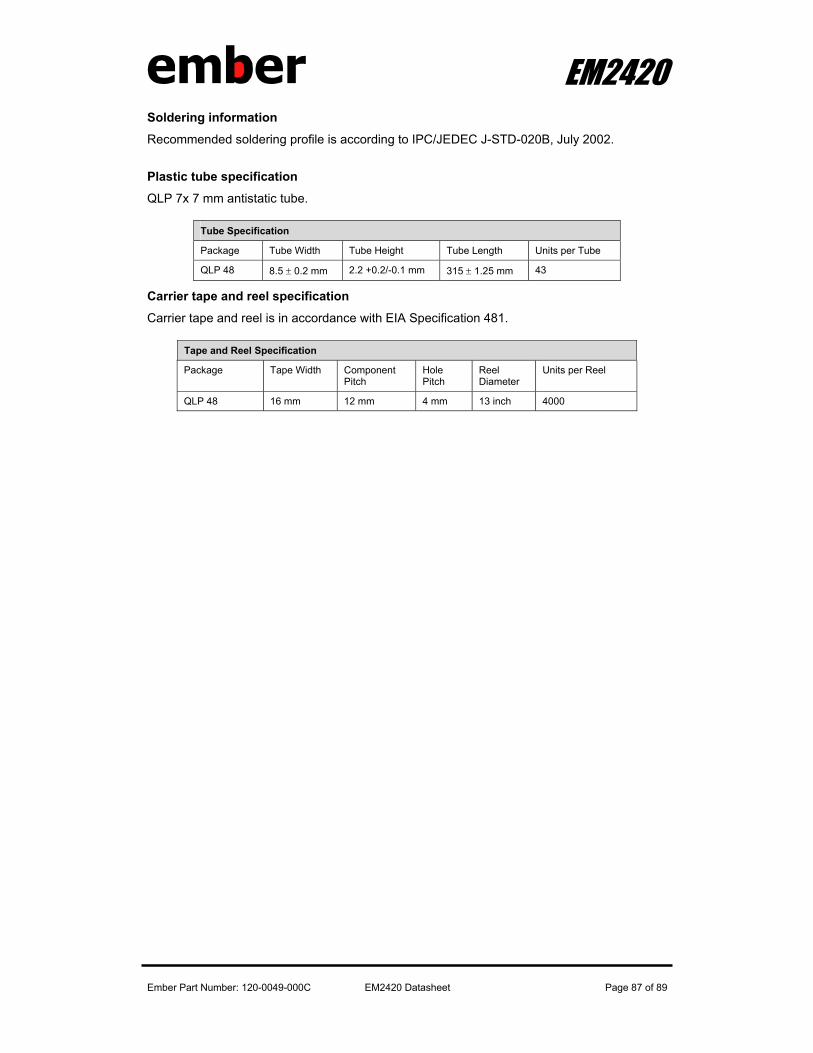
EM2420
Ember Part Number: 120-0049-000C EM2420 Datasheet Page 87 of 89
Soldering information
Recommended soldering profile is according to IPC/JEDEC J-STD-020B, July 2002.
Plastic tube specification
QLP 7x 7 mm antistatic tube.
Tube Specification
Package Tube Width Tube Height Tube Length Units per Tube
QLP 48 8.5 ± 0.2 mm 2.2 +0.2/-0.1 mm 315 ± 1.25 mm 43
Carrier tape and reel specification
Carrier tape and reel is in accordance with EIA Specification 481.
Tape and Reel Specification
Package Tape Width Component Pitch
Hole Pitch
Reel Diameter
Units per Reel
QLP 48 16 mm 12 mm 4 mm 13 inch 4000
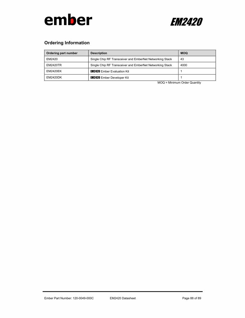
EM2420
Ember Part Number: 120-0049-000C EM2420 Datasheet Page 88 of 89
Ordering Information
Ordering part number Description MOQ
EM2420 Single Chip RF Transceiver and EmberNet Networking Stack 43
EM2420TR Single Chip RF Transceiver and EmberNet Networking Stack 4000
EM2420EK EM2420 Ember Evaluation Kit 1
EM2420DK EM2420 Ember Developer Kit 1
MOQ = Minimum Order Quantity
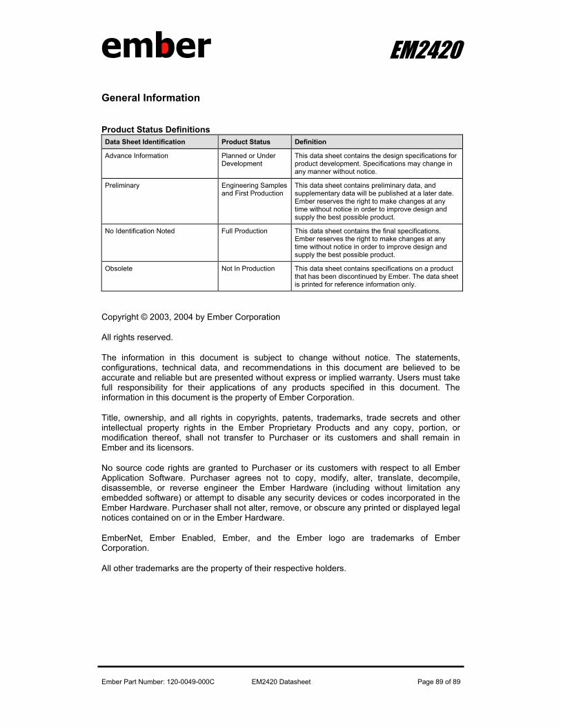
EM2420
Ember Part Number: 120-0049-000C EM2420 Datasheet Page 89 of 89
General Information
Product Status Definitions Data Sheet Identification Product Status Definition
Advance Information Planned or Under Development
This data sheet contains the design specifications for product development. Specifications may change in any manner without notice.
Preliminary Engineering Samples and First Production
This data sheet contains preliminary data, and supplementary data will be published at a later date. Ember reserves the right to make changes at any time without notice in order to improve design and supply the best possible product.
No Identification Noted Full Production This data sheet contains the final specifications. Ember reserves the right to make changes at any time without notice in order to improve design and supply the best possible product.
Obsolete Not In Production This data sheet contains specifications on a product that has been discontinued by Ember. The data sheet is printed for reference information only.
Copyright © 2003, 2004 by Ember Corporation
All rights reserved.
The information in this document is subject to change without notice. The statements, configurations, technical data, and recommendations in this document are believed to be accurate and reliable but are presented without express or implied warranty. Users must take full responsibility for their applications of any products specified in this document. The information in this document is the property of Ember Corporation.
Title, ownership, and all rights in copyrights, patents, trademarks, trade secrets and other intellectual property rights in the Ember Proprietary Products and any copy, portion, or modification thereof, shall not transfer to Purchaser or its customers and shall remain in Ember and its licensors.
No source code rights are granted to Purchaser or its customers with respect to all Ember Application Software. Purchaser agrees not to copy, modify, alter, translate, decompile, disassemble, or reverse engineer the Ember Hardware (including without limitation any embedded software) or attempt to disable any security devices or codes incorporated in the Ember Hardware. Purchaser shall not alter, remove, or obscure any printed or displayed legal notices contained on or in the Ember Hardware.
EmberNet, Ember Enabled, Ember, and the Ember logo are trademarks of Ember Corporation.
All other trademarks are the property of their respective holders.


![ZigBee Stack Profile: Platform restrictions for compliant ...read.pudn.com/.../3...ZigBee-Feature-Set-Profile.pdf · 11 [R2] ZigBee 04140r05, ZigBee Protocol Stack Settable Values](https://img.dokumen.tips/doc/110x75/5f183a7d6417c0751a61665e/zigbee-stack-profile-platform-restrictions-for-compliant-readpudncom3zigbee-feature-set-.jpg)


![AT08550: ZigBee Attribute Reporting · ZigBee Attribute Reporting [APPLICATION NOTE] Atmel-42334A-ZigBee-Attribute-Reporting -ApplicationNote_012015 3 1 Overview The ZigBee Specification](https://img.dokumen.tips/doc/110x75/5f43d267b58b3c15740a0db6/at08550-zigbee-attribute-reporting-zigbee-attribute-reporting-application-note.jpg)


![ZigBee RF4CE Stack User Guide - NXP Semiconductors · 094945r00ZB ZigBee RF4CE Specification [ZigBee Alliance document] 094950r00ZB ZigBee RF4CE Device Type List [ZigBee Alliance](https://img.dokumen.tips/doc/110x75/5f168d2f412bb13bb1076764/zigbee-rf4ce-stack-user-guide-nxp-semiconductors-094945r00zb-zigbee-rf4ce-specification.jpg)