Embed Size (px)
Citation preview
Fall 2016
EGC220 - Digital Logic Fundamentals
VERILOG Hardware Description Language - 1
Hardware description language is a text based programming language that is used to model a piece of hardware. VERILOG is a hardware Description Language; a textual format for describing electronic circuits and systems. It was first developed by Gateway DESIGN Automation in 1984, and later was acquired by Cadence Design Systems in 1989. In 1995 VERILOG was adopted as an IEEE standard (1364). An enhanced version was published in 2001. Even though originally it was intended for simulation and verification of digital circuits only, in recent years CAD tools are used to synthesize the VERILOG code into a hardware implementation of the described circuit. A logic circuit can conveniently be described by a VERILOG source code. The VERILOG compiler translates this code into a logic circuit. VERILOG allows the designer to represent circuits in two different ways: structural representation, and behavioral representation. At the structural level, the levels of abstraction are at the module level, the gate level, the switch level (transistor) or the circuit level. In behavioral representation, a circuit is described by its input/output response, or by logic expressions and programming constructs that defines the behavior of the circuit.
A design is described in VERILOG using the concept of a module. A module can be conceptualized as consisting of two parts, the port declarations and the module body. The port declarations represent the external interface to the module (I/O ports). The module body represents the internal description of the module - its behavior, its structure, or a mixture of both. Each PORT has an associated mode that specifies whether it is an input (input) to the module or an output (output) from the module or inout (bidirectional). Each port represents a signal; hence it has an associated type.
VERILOG is case sensitive and all keywords in VERILOG use lower case letters. The names of modules and signals follow two simple rules: the name must start with a letter and it can contain any letter or number, as well as the underscore ‘_’ and ‘$’ characters. It cannot be a VERILOG keyword. VERILOG allows multiple statements on a single line. Each statement ends with a semicolon. Space, Tab and blank lines are ignored. Comment starts with the double slash “//” character and continues to the end of the line. Multi line comments can be introduced with in the tokens “/*” and “*/” as in C language. VERILOG uses 4 valued logic: 0, 1, x and z, where x represents don’t care and z represents high impedance condition. VERILOG has built-in support for the commonly used logic functions: and, or, not, xor, xnor, nand, and nor. A logic function is represented by its functional name, followed by the output, and inputs in parentheses, in that order. For example, the statement “and (f,a,b)” represents a logical 2-input AND function that generates the output f = AB.
A Simple Design
Let's imagine we want to describe an and-or-invert (AOI) gate in Verilog.
Fall 2016
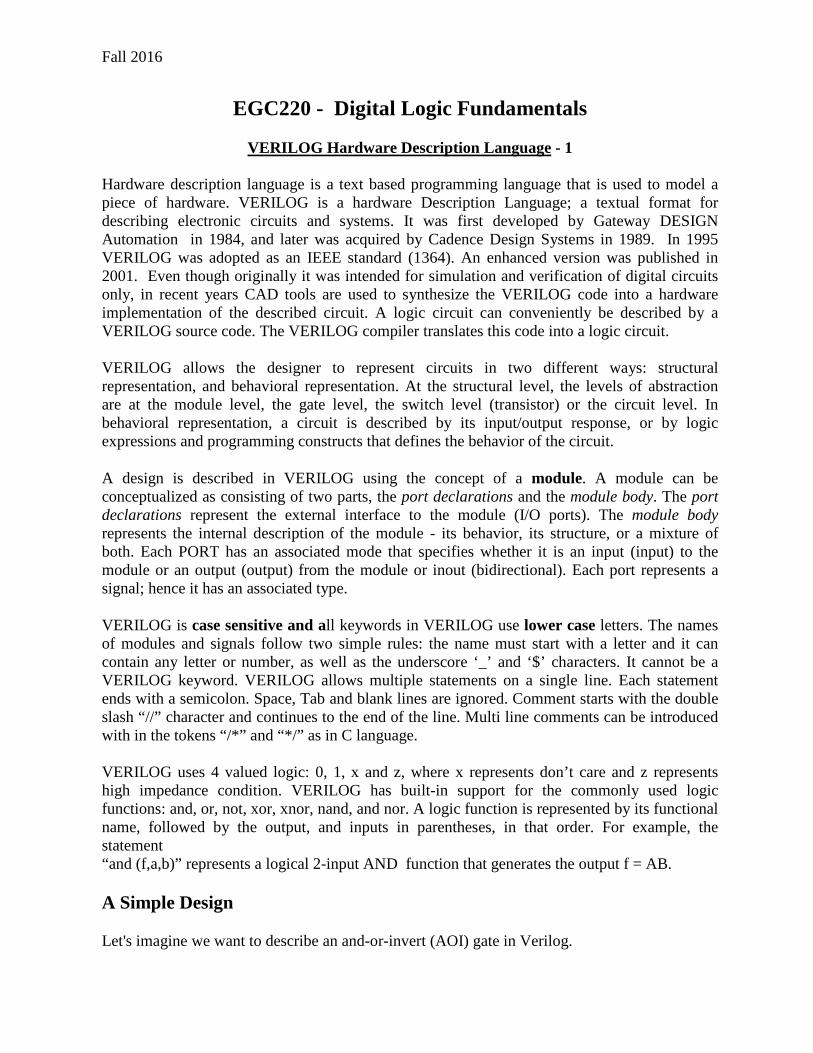
Figure 1: An AOI gate module
// Verilog code for AND-OR-INVERT gate module AOI (input A, B, C, D, output F); assign F = ~((A & B) | (C & D)); endmodule // end of Verilog code
OK, that's the code. Let's dissect it line by line...
Comments
// Verilog code for AND-OR-INVERT gate
Like all programming languages, Verilog supports comments. There are two types of comment in Verilog, line comments and block comments; we will look at line comments for now. Comments are not part of the Verilog design, but allow the user to make notes referring to the Verilog code, usually as an aid to understanding it. Here the comment is a “header” that tells us that the Verilog describes an AOI gate. It is no more than an aide de memoire in this case. A Verilog compiler will ignore this line of Verilog. Two forward slashes mark the start of a line comment, which is ignored by the Verilog compiler. A line comment can be on a separate line or at the end of a line of Verilog code, but in any case stops at the end of the line.
Module and Port declarations
module AOI (input A, B, C, D, output F);
The name of the module is just an arbitrary label invented by the user. It does not correspond to a name pre-defined in a Verilog component library. module is a Verilog keyword. This line defines the start of a new Verilog module definition. All of the input and output ports of the module must appear in parentheses after the module name. The ordering of ports is not important for the module definition per se, although it is conventional to specify input ports first.
A port may correspond to a pin on an IC, an edge connector on a board, or any logical channel of communication with a block of hardware. The port declarations include the names of the ports ( e.g., A, B ), and the direction that information is allowed to flow through the ports (input, output or inout).
Fall 2016
endmodule
endmodule
The module definition is terminated by the Verilog keyword endmodule.
Functionality
Well, that's the interface to the module taken care of, but what about its functionality?
assign F = ~((A & B) | (C & D));
In this module body, there is but one statement, and all the names referenced in this statement are in fact the ports of the design. Because all of the names used in the module body are declared in the module header and port declarations, there are no further declarations for internal elements required in the module body. assign is a Verilog keyword. It denotes a concurrent continuous assignment, which describes the functionality of the module. The concurrent assignment executes whenever one of the four ports A, B, C or D change value. The ~, & and | symbols represent the bit-wise not, and and or operators respectively, which are built in to the Verilog language. That's it! That's all there is to describing the functionality of an AOI gate in Verilog.
// end of Verilog code
Another Verilog comment, and that's the end of a Verilog description for an AOI gate.
Verilog 1995
The above example is written using Verilog-2001 syntax. Many people continue to use the 1995 syntax, which is still allowed in Verilog-2001. In Verilog-1995 the module header would look like this:
module AOI (A, B, C, D, F); input A, B, C, D; output F;
Note that the port names are listed after the module name, and declared as inputs and outputs in separate statements. The port declarations must repeat the names of the ports in the module header.
Wires
The module shown on the “Modules” page, was simple enough to describe using a continuous assignment where the output was a function of the inputs. Usually, modules are more complex than this, and internal connections are required. To make a continuous assignment to an internal signal, the signal must first be declared as a wire.
Fall 2016
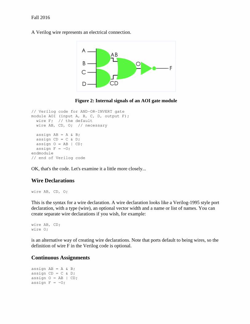
A Verilog wire represents an electrical connection.
Figure 2: Internal signals of an AOI gate module
// Verilog code for AND-OR-INVERT gate module AOI (input A, B, C, D, output F); wire F; // the default wire AB, CD, O; // necessary assign AB = A & B; assign CD = C & D; assign O = AB | CD; assign F = ~O; endmodule // end of Verilog code
OK, that's the code. Let's examine it a little more closely...
Wire Declarations
wire AB, CD, O;
This is the syntax for a wire declaration. A wire declaration looks like a Verilog-1995 style port declaration, with a type (wire), an optional vector width and a name or list of names. You can create separate wire declarations if you wish, for example:
wire AB, CD; wire O; is an alternative way of creating wire declarations. Note that ports default to being wires, so the definition of wire F in the Verilog code is optional.
Continuous Assignments
assign AB = A & B; assign CD = C & D; assign O = AB | CD; assign F = ~O;
Fall 2016
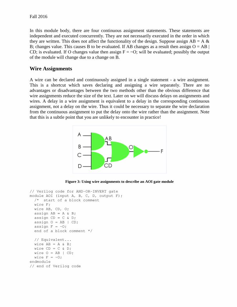
In this module body, there are four continuous assignment statements. These statements are independent and executed concurrently. They are not necessarily executed in the order in which they are written. This does not affect the functionality of the design. Suppose assign AB = A & B; changes value. This causes B to be evaluated. If AB changes as a result then assign O = AB | CD; is evaluated. If O changes value then assign F = ~O; will be evaluated; possibly the output of the module will change due to a change on B.
Wire Assignments
A wire can be declared and continuously assigned in a single statement - a wire assignment. This is a shortcut which saves declaring and assigning a wire separately. There are no advantages or disadvantages between the two methods other than the obvious difference that wire assignments reduce the size of the text. Later on we will discuss delays on assignments and wires. A delay in a wire assignment is equivalent to a delay in the corresponding continuous assignment, not a delay on the wire. Thus it could be necessary to separate the wire declaration from the continuous assignment to put the delay onto the wire rather than the assignment. Note that this is a subtle point that you are unlikely to encounter in practice!
Figure 3: Using wire assignments to describe an AOI gate module
// Verilog code for AND-OR-INVERT gate module AOI (input A, B, C, D, output F); /* start of a block comment wire F; wire AB, CD, O; assign AB = A & B; assign CD = C & D; assign O = AB | CD; assign F = ~O; end of a block comment */ // Equivalent... wire AB = A & B; wire CD = C & D; wire O = AB | CD; wire F = ~O; endmodule // end of Verilog code
Fall 2016
So in this sample code, each of the wire declarations and its corresponding assign statement are effectively merged into one wire assignment.
Note the use of a block comment in the Verilog code, rather than the line comments we have seen so far. A block comment may span several lines of code. Block comments may not be nested.
A Design Hierarchy
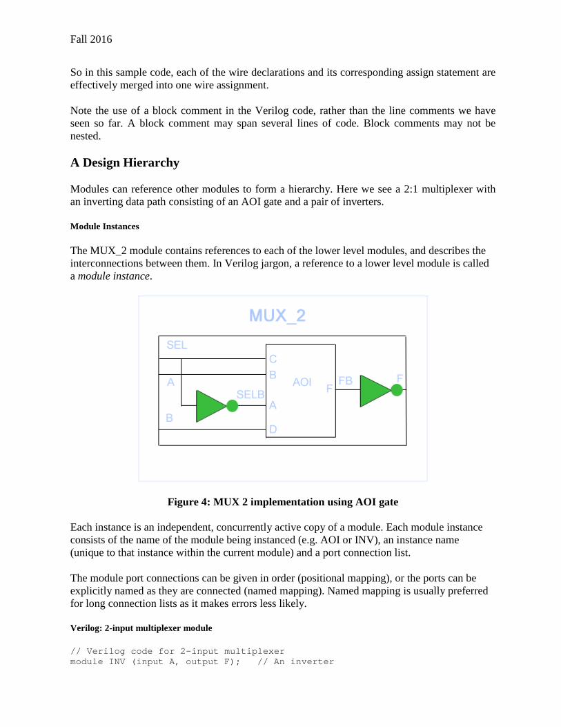
Modules can reference other modules to form a hierarchy. Here we see a 2:1 multiplexer with an inverting data path consisting of an AOI gate and a pair of inverters.
Module Instances
The MUX_2 module contains references to each of the lower level modules, and describes the interconnections between them. In Verilog jargon, a reference to a lower level module is called a module instance.
Figure 4: MUX 2 implementation using AOI gate
Each instance is an independent, concurrently active copy of a module. Each module instance consists of the name of the module being instanced (e.g. AOI or INV), an instance name (unique to that instance within the current module) and a port connection list.
The module port connections can be given in order (positional mapping), or the ports can be explicitly named as they are connected (named mapping). Named mapping is usually preferred for long connection lists as it makes errors less likely.
Verilog: 2-input multiplexer module
// Verilog code for 2-input multiplexer module INV (input A, output F); // An inverter
Fall 2016
assign F = ~A; endmodule module AOI (input A, B, C, D, output F); assign F = ~((A & B) | (C & D)); endmodule module MUX2 (input SEL, A, B, output F); // 2:1 multiplexer // wires SELB and FB are implicit // Module instances... INV G1 (SEL, SELB); AOI G2 (SELB, A, SEL, B, FB); INV G3 (.A(FB), .F(F)); // Named mapping endmodule // end of Verilog code
Yes, it's time to dissect the code line by line again, but we'll concentrate on the new lines as the module interface has been covered before (see A Simple Design).
Implicit Wires
// wires SELB and FB are implicit
The wires used in continuous assignments MUST be declared. However, one-bit wires connecting component instances together do not need to be declared. Such wires are regarded as implicit wires. Note that implicit wires are only one bit wide, if a connection between two components is a bus, you must declare the bus as a wire.
Module Instances
AOI G2 (SELB, A, SEL, B, FB);
In a module instance, the ports defined in the module interface are connected to wires in the instantiating module through the use of port mapping. For the instance of AOI, the first wire in the port list is SELB. In the module header for the AOI gate, A is the first port in the port list, so SELB is connected to A. The second port in the module header is B, the second wire in the port list is A, thus the wire A in MUX2 is connected to the port B of the AOI gate instance.
INV G3 (.A(FB), .F(F));
The second INV instance, G3, uses named mapping rather than positional mapping. In the port list for the G£ instance, the wire FB is connected to the input port, A, of the INV instance. The period character is followed by the name of the module header port; in brackets following the formal port, the name of the wire is entered.
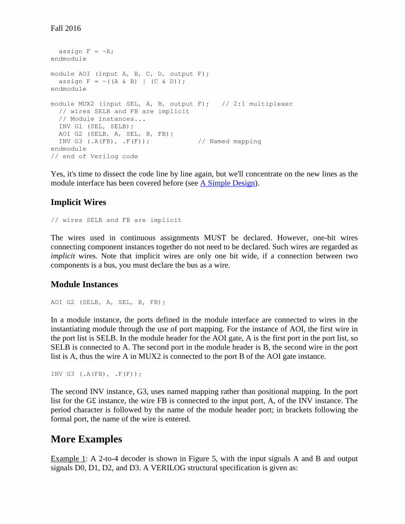
More Examples Example 1: A 2-to-4 decoder is shown in Figure 5, with the input signals A and B and output signals D0, D1, D2, and D3. A VERILOG structural specification is given as:
Fall 2016
module decoder (A,B, D0,D1,D2,D3); input A,B; output D0,D1,D2,D3;
and (D0,~A,~B); and (D1,~A,B); and (D2,A,~B); and (D3,A,B);
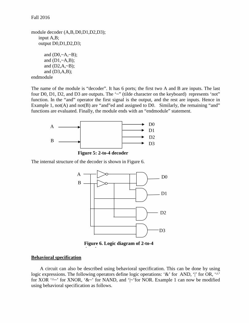
endmodule The name of the module is “decoder”. It has 6 ports; the first two A and B are inputs. The last four D0, D1, D2, and D3 are outputs. The ‘~” (tilde character on the keyboard) represents ‘not” function. In the “and” operator the first signal is the output, and the rest are inputs. Hence in Example 1, not(A) and not(B) are “and”ed and assigned to D0. Similarly, the remaining “and” functions are evaluated. Finally, the module ends with an “endmodule” statement. The internal structure of the decoder is shown in Figure 6.
Behavioral specification
A circuit can also be described using behavioral specification. This can be done by using
logic expressions. The following operators define logic operations: ‘&’ for AND, ‘|’ for OR, ‘^’ for XOR ‘^~’ for XNOR, ‘&~’ for NAND, and ‘|~’for NOR. Example 1 can now be modified using behavioral specification as follows.
D0 B
A
D1
D2
D3
Figure 6. Logic diagram of 2-to-4 d d
Figure 5: 2-to-4 decoder
A
B
D0 D1 D2 D3
Fall 2016
module decoder (A,B, D0,D1,D2,D3); input A,B; output D0,D1,D2,D3;
assign D0 = ~A&~B; assign D1 = ~A&B; assign D2 = A&~B; assign D3 = A&B;
endmodule
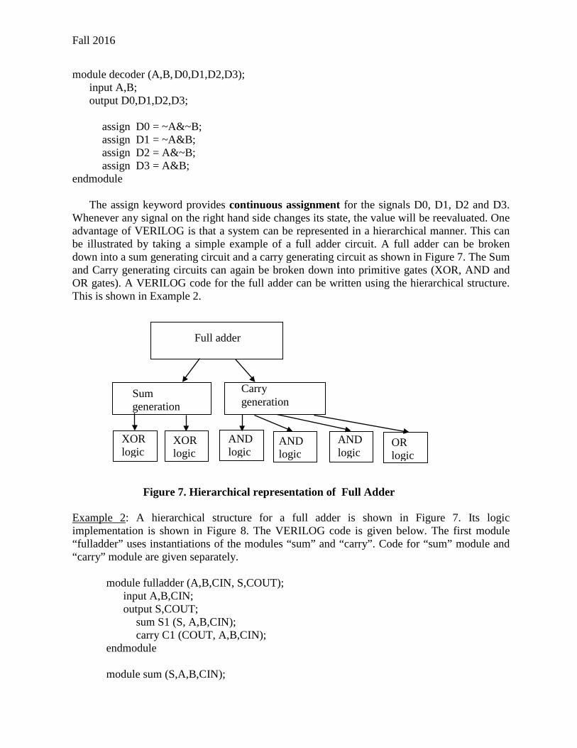
The assign keyword provides continuous assignment for the signals D0, D1, D2 and D3. Whenever any signal on the right hand side changes its state, the value will be reevaluated. One advantage of VERILOG is that a system can be represented in a hierarchical manner. This can be illustrated by taking a simple example of a full adder circuit. A full adder can be broken down into a sum generating circuit and a carry generating circuit as shown in Figure 7. The Sum and Carry generating circuits can again be broken down into primitive gates (XOR, AND and OR gates). A VERILOG code for the full adder can be written using the hierarchical structure. This is shown in Example 2.
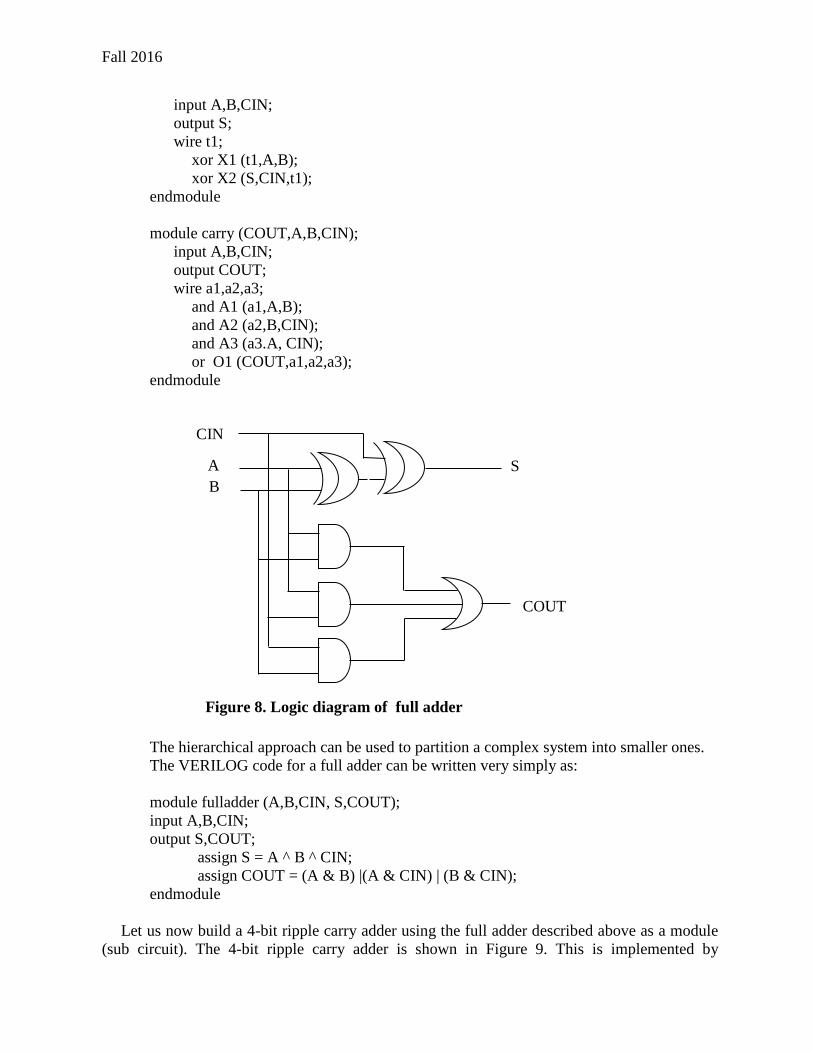
Example 2: A hierarchical structure for a full adder is shown in Figure 7. Its logic implementation is shown in Figure 8. The VERILOG code is given below. The first module “fulladder” uses instantiations of the modules “sum” and “carry”. Code for “sum” module and “carry” module are given separately.
module fulladder (A,B,CIN, S,COUT); input A,B,CIN; output S,COUT;
sum S1 (S, A,B,CIN); carry C1 (COUT, A,B,CIN);
endmodule module sum (S,A,B,CIN);
Figure 7. Hierarchical representation of Full Adder
Full adder
Carry generation
AND logic
AND logic
Sum generation
XOR logic
XOR logic
AND logic
OR logic
Fall 2016
input A,B,CIN; output S; wire t1;
xor X1 (t1,A,B); xor X2 (S,CIN,t1);
endmodule module carry (COUT,A,B,CIN);
input A,B,CIN; output COUT; wire a1,a2,a3;
and A1 (a1,A,B); and A2 (a2,B,CIN); and A3 (a3.A, CIN); or O1 (COUT,a1,a2,a3);
endmodule The hierarchical approach can be used to partition a complex system into smaller ones. The VERILOG code for a full adder can be written very simply as: module fulladder (A,B,CIN, S,COUT); input A,B,CIN; output S,COUT;
assign S = A ^ B ^ CIN; assign COUT = (A & B) |(A & CIN) | (B & CIN);
endmodule
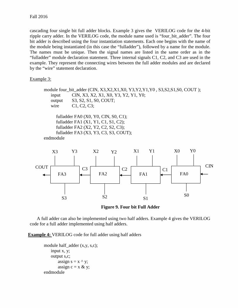
Let us now build a 4-bit ripple carry adder using the full adder described above as a module (sub circuit). The 4-bit ripple carry adder is shown in Figure 9. This is implemented by
S B A
COUT
CIN
Figure 8. Logic diagram of full adder
Fall 2016
cascading four single bit full adder blocks. Example 3 gives the VERILOG code for the 4-bit ripple carry adder. In the VERILOG code, the module name used is “four_bit_adder”. The four bit adder is described using the four instantiation statements. Each one begins with the name of the module being instantiated (in this case the “fulladder”), followed by a name for the module. The names must be unique. Then the signal names are listed in the same order as in the “fulladder” module declaration statement. Three internal signals C1, C2, and C3 are used in the example. They represent the connecting wires between the full adder modules and are declared by the “wire” statement declaration. Example 3:
module four_bit_adder (CIN, X3,X2,X1,X0, Y3,Y2,Y1,Y0 , S3,S2,S1,S0, COUT );
input CIN, X3, X2, X1, X0, Y3, Y2, Y1, Y0; output S3, S2, S1, S0, COUT; wire C1, C2, C3;
fulladder FA0 (X0, Y0, CIN, S0, C1); fulladder FA1 (X1, Y1, C1, S1, C2); fulladder FA2 (X2, Y2, C2, S2, C3); fulladder FA3 (X3, Y3, C3, S3, COUT);
endmodule
A full adder can also be implemented using two half adders. Example 4 gives the VERILOG code for a full adder implemented using half adders.
Example 4: VERILOG code for full adder using half adders
module half_adder (x,y, s,c);
input x, y; output s,c;
assign s = x ^ y; assign c = x & y;
endmodule
FA0 FA1 FA2 FA3
Y0 Y1 Y2 Y3 X0 X1 X2 X3
S0 S1 S2 S3
C1 C2 C3 CIN COUT
Figure 9. Four bit Full Adder
Fall 2016
module full_adder (x, y, z, s, c); input x,y,z; output s,c: wire hs, hc, tc;
half _adder HA0 (x, y, hs, hc); half _adder HA1 (hs, z, s, tc); assign c = tc | hc;
endmodule
The VERILOG code for the 4-bit ripple-carry-adder can be written using vector notation. Example 5 illustrates this. The full adder in Example 4 is used in Example 5. The statement “input [3:0] A, B” means that A and B are 4-bit inputs with their MSB’s A(3) and B(3) and LSB’s A(0) and B(0) respectively. We can change the order of MSB and LSB by specifying “input [0:3] A, B”, in which case A(0) and B(0) become MSB bits.
Example 5:
module adder_4 (B, A,CIN,S ,COUT); input [3:0] A,B; input CIN; output [3:0] S; output COUT; wire [4:0] C;
full _adder FA0 (B(0), A(0), C(0), S(0), C(1)); full _adder FA1 (B(1), A(1), C(1), S(1), C(2)); full _adder FA2 (B(2), A(2), C(2), S(2), C(3)); full _adder FA3 (B(3), A(3), C(3), S(3), C(4)); assign C(0) = CIN; assign COUT = C(4);
endmodule
Conditional Statement Conditional_expression ? true_expression : false expression; Example 6: Assign A = (B<C) ? (D+5) : (D+2); means that if B is less than C, the value of A will be D + 5, or else A will have the value D + 2. Procedural Statement
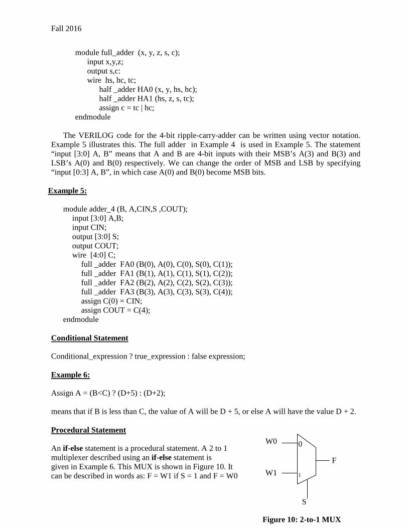
An if-else statement is a procedural statement. A 2 to 1 multiplexer described using an if-else statement is given in Example 6. This MUX is shown in Figure 10. It can be described in words as: F = W1 if S = 1 and F = W0
Figure 10: 2-to-1 MUX
W0
W1
S
F
0
1
Fall 2016
if S =0. In VERILOG this behavior can be described as: if (S==1) F = W1; else F = W0;
Example 6: MUX 2-to-1
//Behavioral specification module mux2to1 (w0, w1, s, F);
input wo,w1,s; output F; reg F;
always @ (w0,w1,s) if (s==1) F = w1; else F = w0; endmodule
VERILOG syntax requires that procedural statements be contained inside a construct called
an “always” block. An “always” block can contain a single statement or a number of statements. A typical VERILOG module may include several “always” blocks. The statements in an “always” block are evaluated in the order given in the code. This is in contrast to the continuous assignment statements, which are evaluated concurrently and hence have no meaningful order. The part of the always block after the @ symbol, in parentheses, is called the sensitivity list. The statements inside an always block are executed by the simulator only when one or more of the signals in the sensitivity list change in value. If a signal is assigned a value using procedural statements, then VERILOG syntax requires that it be declared as a variable, this is accomplished by using the keyword “reg”. This means that once the variable value is assigned, the simulator “registers” this value and it will not change until the “always” block is executed again.
Numbers in Verilog
Constants can be specified in decimal, octal, hexadecimal or binary format. Negative
numbers are represented in 2’s complement format. The syntax is: <size>’<radix><value> The character “ ’ ” after <size> is read as “tick”. The default size value is 32 bits. Examples: 8’hA7represents an 8 bit hexadecimal number 10100111. 7’b100101 represents a 7 bit number 0100101. When the size is larger than the value (as in this example), the leftmost bits are filled based on the value of the given number. When the leftmost bit is 0 or 1, then a 0 is used. Z are filled with Z and X with X. 2 is represented by the default 32 bit number “00000000000000000000000000000010”
Example 7: Mux 4-to-1
Fall 2016
module mux4to1 (w0, w1,w2, w3, S, F); input w0,w1,w2,w3,[1:0] S; output F; reg F;
always @ (w0,w1,w2,w3,S) if (S==0) F = w0; else if (S==1) F = w1; else if (S==2) F = w2; else F = w3; endmodule
Test Benches
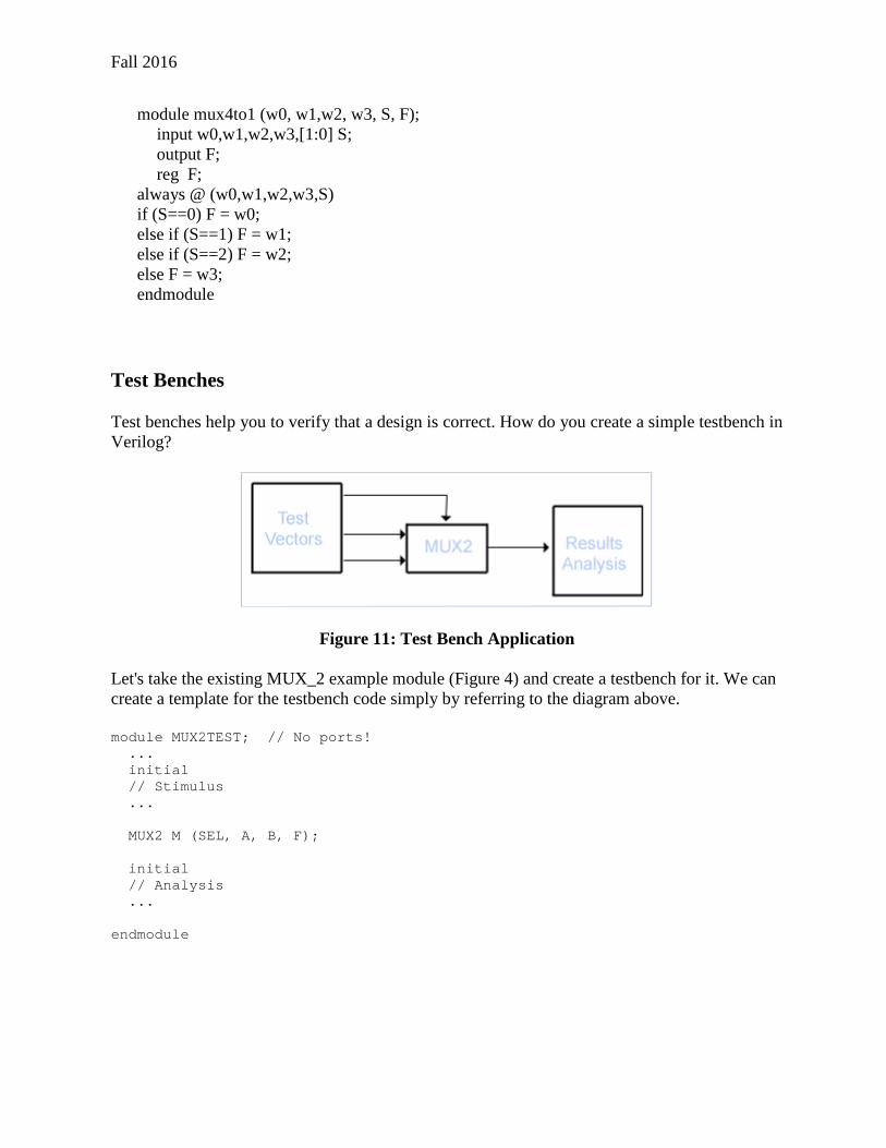
Test benches help you to verify that a design is correct. How do you create a simple testbench in Verilog?
Figure 11: Test Bench Application
Let's take the existing MUX_2 example module (Figure 4) and create a testbench for it. We can create a template for the testbench code simply by referring to the diagram above.
module MUX2TEST; // No ports! ... initial // Stimulus ... MUX2 M (SEL, A, B, F); initial // Analysis ... endmodule
Fall 2016
Initial Statement
In this code fragment, the stimulus and response capture are going to be coded using a pair of initial blocks. An initial block can contain sequential statements that can be used to describe the behavior of signals in a test bench.
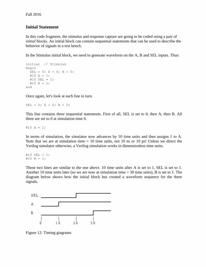
In the Stimulus initial block, we need to generate waveform on the A, B and SEL inputs. Thus:
initial // Stimulus begin SEL = 0; A = 0; B = 0; #10 A = 1; #10 SEL = 1; #10 B = 1; end
Once again, let's look at each line in turn.
SEL = 0; A = 0; B = 0;
This line contains three sequential statements. First of all, SEL is set to 0, then A, then B. All three are set to 0 at simulation time 0.
#10 A = 1;
In terms of simulation, the simulator now advances by 10 time units and then assigns 1 to A. Note that we are at simulation time = 10 time units, not 10 ns or 10 ps! Unless we direct the Verilog simulator otherwise, a Verilog simulation works in dimensionless time units.
#10 SEL = 1; #10 B = 1;
These two lines are similar to the one above. 10 time units after A is set to 1, SEL is set to 1. Another 10 time units later (so we are now at simulation time = 30 time units), B is set to 1. The diagram below shows how the initial block has created a waveform sequence for the three signals.
Figure 12: Timing giagrams
Fall 2016
We shall look at the use of the initial block to capture the MUX_2's response in the next section of the tutorial.
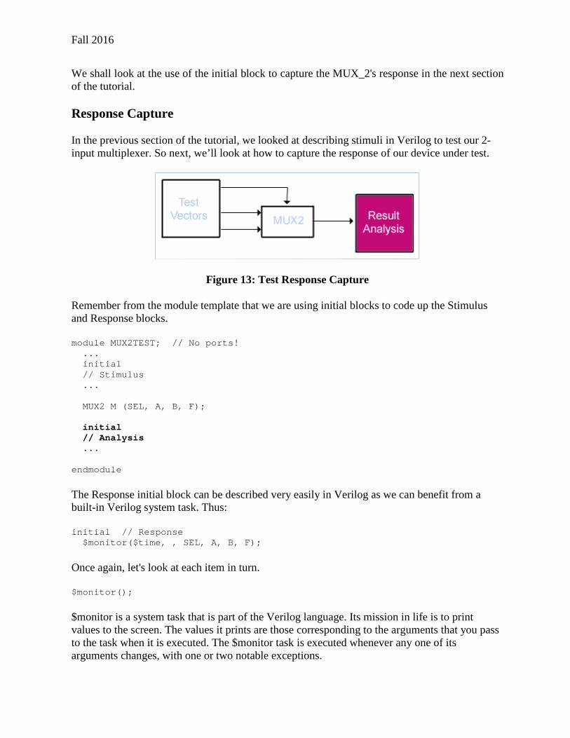
Response Capture
In the previous section of the tutorial, we looked at describing stimuli in Verilog to test our 2-input multiplexer. So next, we’ll look at how to capture the response of our device under test.
Figure 13: Test Response Capture
Remember from the module template that we are using initial blocks to code up the Stimulus and Response blocks.
module MUX2TEST; // No ports! ... initial // Stimulus ... MUX2 M (SEL, A, B, F); initial // Analysis ... endmodule
The Response initial block can be described very easily in Verilog as we can benefit from a built-in Verilog system task. Thus:
initial // Response $monitor($time, , SEL, A, B, F);
Once again, let's look at each item in turn.
$monitor();
$monitor is a system task that is part of the Verilog language. Its mission in life is to print values to the screen. The values it prints are those corresponding to the arguments that you pass to the task when it is executed. The $monitor task is executed whenever any one of its arguments changes, with one or two notable exceptions.
Fall 2016
$time
$time is a system function (as opposed to a system task). It returns the current simulation time. In the above example, $time is an argument to $monitor. However, $time changing does not cause $monitor to execute - $monitor is clever enough to know that you wouldn't really want to print to the screen the values of all of the arguments every time the simulation time changed.
, , ,
The space at position 2 in the argument list ensures that a space is printed to the screen after the value of $time each time $monitor is executed. This is a simple method of formatting the screen output.
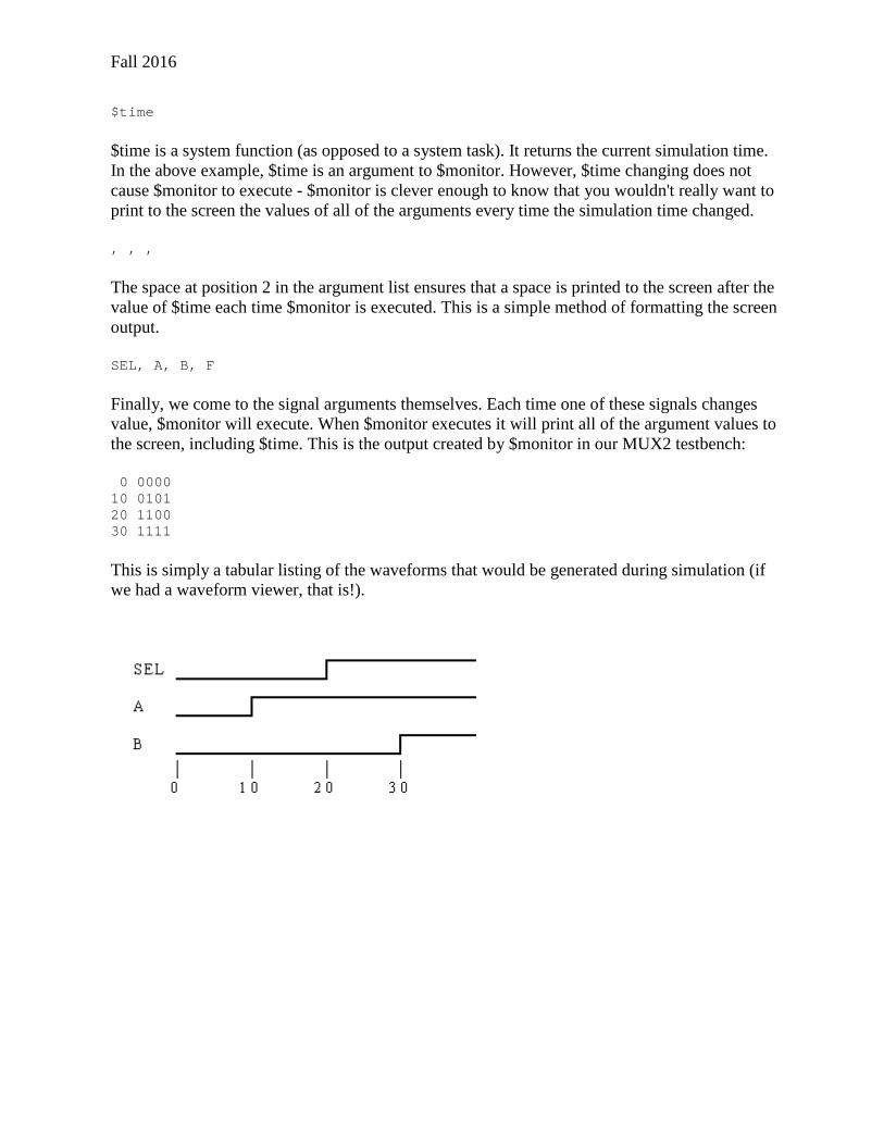
SEL, A, B, F
Finally, we come to the signal arguments themselves. Each time one of these signals changes value, $monitor will execute. When $monitor executes it will print all of the argument values to the screen, including $time. This is the output created by $monitor in our MUX2 testbench:
0 0000 10 0101 20 1100 30 1111
This is simply a tabular listing of the waveforms that would be generated during simulation (if we had a waveform viewer, that is!).
Fall 2016
RTL Verilog
Remember this?
Now we are going to look at the principles of RTL coding for synthesis tools. Most commercially available synthesis tools expect to be given a design description in RTL form. RTL is an acronym for register transfer level. This implies that your Verilog code describes how data is transformed as it is passed from register to register. The transforming of the data is performed by the combinational logic that exists between the registers. Don't worry! RTL code also applies to pure combinational logic - you don't have to use registers. To show you what we mean by RTL code, let's consider a simple example.
module AOI (input A, B, C, D, output F);
assign F = ~((A & B) | (C & D));
endmodule
Yes! The AOI gate that we have used as an example so far has actually been written in RTL form. This means that continuous assignments are a valid way of describing designs for input to RTL synthesis tools. What other code techniques can we use? How about:
module MUX2 (input SEL, A, B, output F);
input SEL, A, B;
output F;
INV G1 (SEL, SELB);
AOI G2 (SELB, A, SEL, B, FB);
INV G3 (.A(FB), .F(F)); endmodule
Fall 2016
Module instances are also examples of synthesizable RTL statements. However, one of the reasons to use synthesis technology is to be able to describe the design at a higher level of abstraction than using a collection of module instances or low-level binary operators in a continuous assignment. We would like to be able to describe what the design does and leave the consideration of how the design is implemented up to the synthesis tool. This is a first step (and a pretty big conceptual one) on the road to high-level design. We are going to use a feature of the Verilog language that allows us to specify the functionality of a design (the ‘what') that can be interpreted by a synthesis tool. Always blocks Always blocks are akin to the initial blocks that you have met already in Test Benches. Initial blocks are procedural blocks that contain sequential statements. Initial blocks execute just once. Always blocks on the other hand are always available for execution. This means that the statements inside an always block are executed up until the closing end keyword:
always
begin
// statements
end
But then they can be executed again! This means that a way of controlling execution through an always block is required. In describing synthesizable designs, a sensitivity list is often used to control execution (we shall see other approaches later).
always @(sensitivity-list)
begin
// statements
end
The sensitivity list consists of one or more signals. When at least one of these signals changes, the always block executes through to the end keyword as before. Except that now, the sensitivity list prevents the always block from executing again until another change occurs on a signal in the sensitivity list. The statements inside the always block describe the functionality of the design (or a part of it). Let's reconsider the AOI gate:
Fall 2016
always @(sensitivity-list)
begin
F = ~((a & b) | (c & d));
end
Instead of a continuous assignment, we now have a procedural assignment to describe the functionality of the AOI gate. Notice that the sensitivity list isn't valid Verilog code. We need to create a meaningful sensitivity list. How do we decide when to execute the always block? Perhaps a better question is what do we need to do in order to have F change value. Answer: F can only change when at least one of a, b, c or d changes. After all, these are the four inputs to the AOI gate. That's our sensitivity list:
always @(a or b or c or d)
begin
F = ~((a & b) | (c & d));
end
Verilog-2001 introduced additional syntax for describing sensitivity lists.
always @(a, b, c, d)
always @(*)
always @*
In the first of these, we have simply replaced the word or with a comma. The other two are equivalent and create an implicit sensitivity list that contains all the signals whose values are read in the statements of the always block. In this example @* or @(*) are equivalent to @(a,b,c,d). When describing combinational logic, it is important to make sure that sensitivity lists are complete; this syntax helps to ensure that this is holds. Now for the MUX_2 design. In the above code snippet, we simply replaced the continuous assignment with an equivalent always block. We can do the same with the module instances in the MUX_2 design - strip away each instance and replace it with the equivalent always block.
Fall 2016
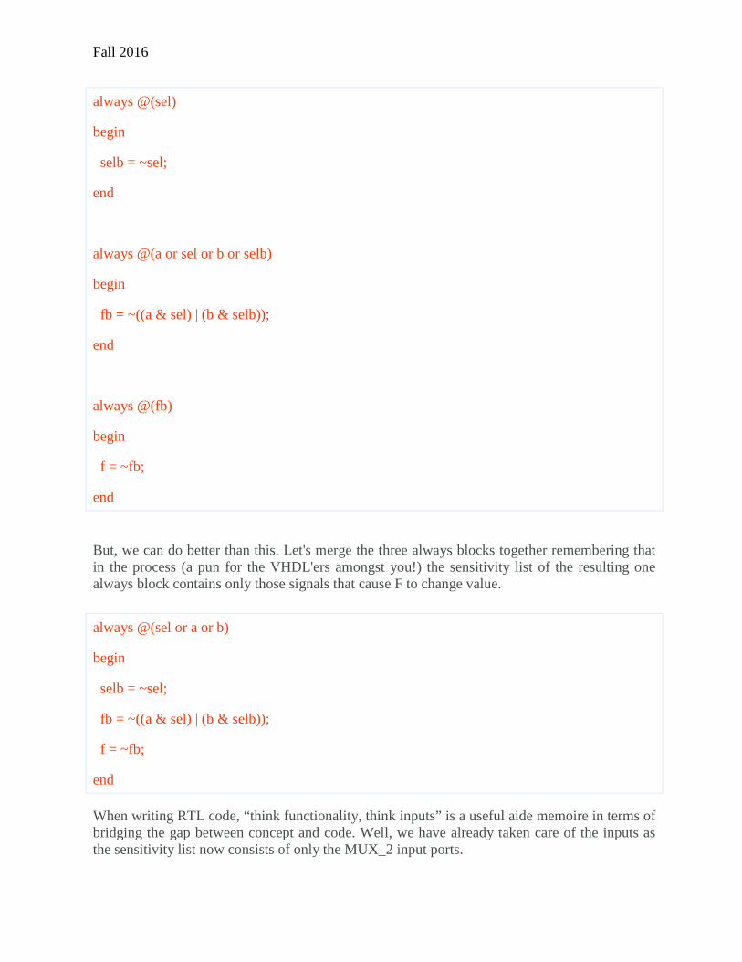
always @(sel)
begin
selb = ~sel;
end
always @(a or sel or b or selb)
begin
fb = ~((a & sel) | (b & selb));
end
always @(fb)
begin
f = ~fb;
end
But, we can do better than this. Let's merge the three always blocks together remembering that in the process (a pun for the VHDL'ers amongst you!) the sensitivity list of the resulting one always block contains only those signals that cause F to change value.
always @(sel or a or b)
begin
selb = ~sel;
fb = ~((a & sel) | (b & selb));
f = ~fb;
end
When writing RTL code, “think functionality, think inputs” is a useful aide memoire in terms of bridging the gap between concept and code. Well, we have already taken care of the inputs as the sensitivity list now consists of only the MUX_2 input ports.
Fall 2016
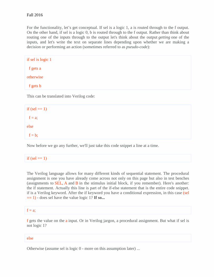
For the functionality, let’s get conceptual. If sel is a logic 1, a is routed through to the f output. On the other hand, if sel is a logic 0, b is routed through to the f output. Rather than think about routing one of the inputs through to the output let's think about the output getting one of the inputs, and let's write the text on separate lines depending upon whether we are making a decision or performing an action (sometimes referred to as pseudo-code):
if sel is logic 1
f gets a
otherwise
f gets b
This can be translated into Verilog code:
if (sel == 1)
f = a;
else
f = b;
Now before we go any further, we'll just take this code snippet a line at a time.
if (sel == 1)
The Verilog language allows for many different kinds of sequential statement. The procedural assignment is one you have already come across not only on this page but also in test benches (assignments to SEL, A and B in the stimulus initial block, if you remember). Here's another: the if statement. Actually this line is part of the if-else statement that is the entire code snippet. if is a Verilog keyword. After the if keyword you have a conditional expression, in this case (sel == 1) - does sel have the value logic 1? If so...
f = a;
f gets the value on the a input. Or in Verilog jargon, a procedural assignment. But what if sel is not logic 1?
else
Otherwise (assume sel is logic 0 - more on this assumption later) ...
Fall 2016
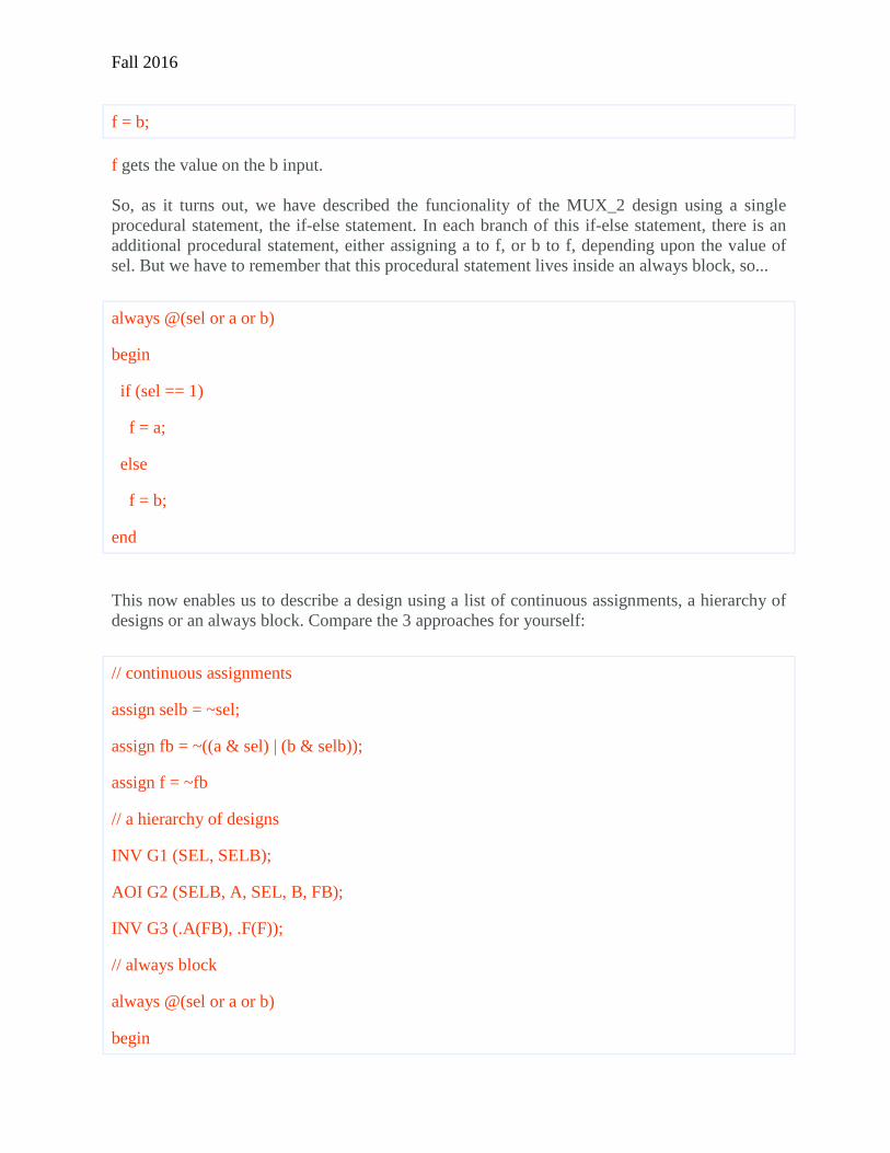
f = b;
f gets the value on the b input. So, as it turns out, we have described the funcionality of the MUX_2 design using a single procedural statement, the if-else statement. In each branch of this if-else statement, there is an additional procedural statement, either assigning a to f, or b to f, depending upon the value of sel. But we have to remember that this procedural statement lives inside an always block, so...
always @(sel or a or b)
begin
if (sel == 1)
f = a;
else
f = b;
end
This now enables us to describe a design using a list of continuous assignments, a hierarchy of designs or an always block. Compare the 3 approaches for yourself:
// continuous assignments
assign selb = ~sel;
assign fb = ~((a & sel) | (b & selb));
assign f = ~fb
// a hierarchy of designs
INV G1 (SEL, SELB);
AOI G2 (SELB, A, SEL, B, FB);
INV G3 (.A(FB), .F(F));
// always block
always @(sel or a or b)
begin
Fall 2016
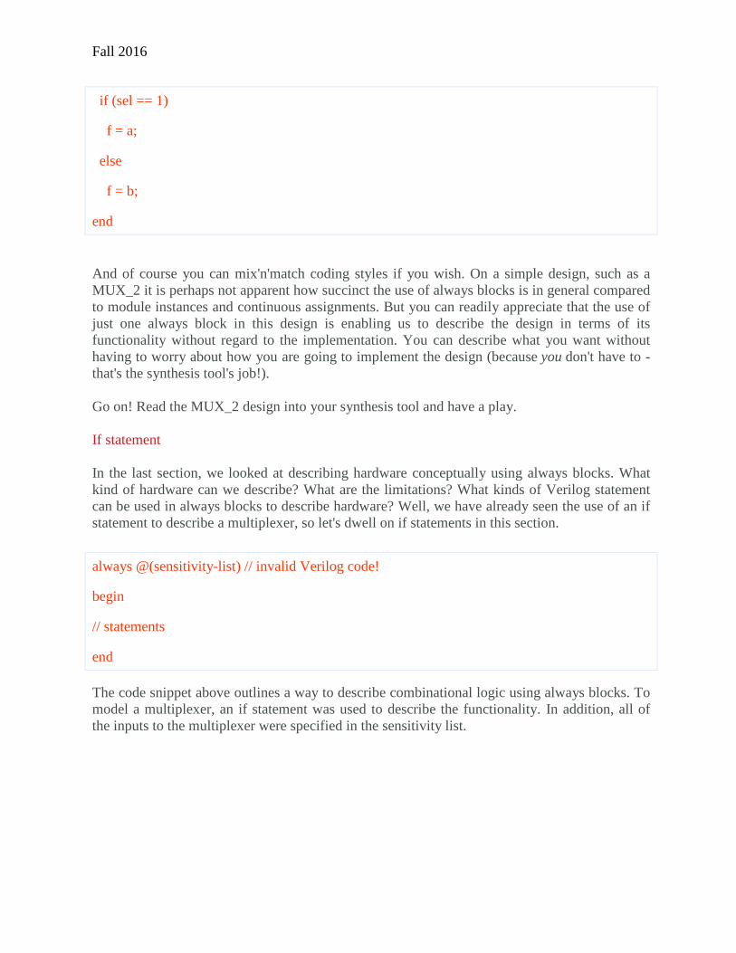
if (sel == 1)
f = a;
else
f = b;
end
And of course you can mix'n'match coding styles if you wish. On a simple design, such as a MUX_2 it is perhaps not apparent how succinct the use of always blocks is in general compared to module instances and continuous assignments. But you can readily appreciate that the use of just one always block in this design is enabling us to describe the design in terms of its functionality without regard to the implementation. You can describe what you want without having to worry about how you are going to implement the design (because you don't have to - that's the synthesis tool's job!). Go on! Read the MUX_2 design into your synthesis tool and have a play. If statement In the last section, we looked at describing hardware conceptually using always blocks. What kind of hardware can we describe? What are the limitations? What kinds of Verilog statement can be used in always blocks to describe hardware? Well, we have already seen the use of an if statement to describe a multiplexer, so let's dwell on if statements in this section.
always @(sensitivity-list) // invalid Verilog code!
begin
// statements
end
The code snippet above outlines a way to describe combinational logic using always blocks. To model a multiplexer, an if statement was used to describe the functionality. In addition, all of the inputs to the multiplexer were specified in the sensitivity list.
Fall 2016
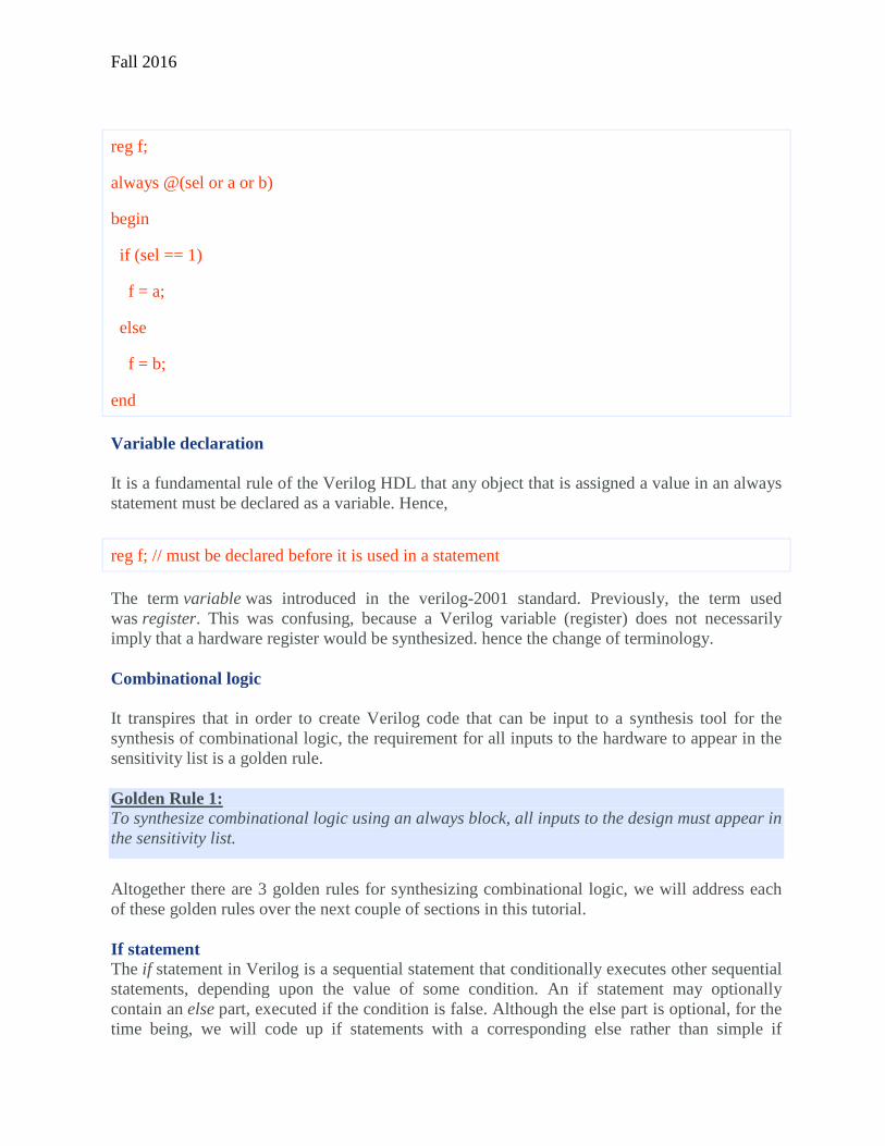
reg f;
always @(sel or a or b)
begin
if (sel == 1)
f = a;
else
f = b;
end
Variable declaration It is a fundamental rule of the Verilog HDL that any object that is assigned a value in an always statement must be declared as a variable. Hence,
reg f; // must be declared before it is used in a statement
The term variable was introduced in the verilog-2001 standard. Previously, the term used was register. This was confusing, because a Verilog variable (register) does not necessarily imply that a hardware register would be synthesized. hence the change of terminology. Combinational logic It transpires that in order to create Verilog code that can be input to a synthesis tool for the synthesis of combinational logic, the requirement for all inputs to the hardware to appear in the sensitivity list is a golden rule. Golden Rule 1: To synthesize combinational logic using an always block, all inputs to the design must appear in the sensitivity list.
Altogether there are 3 golden rules for synthesizing combinational logic, we will address each of these golden rules over the next couple of sections in this tutorial. If statement The if statement in Verilog is a sequential statement that conditionally executes other sequential statements, depending upon the value of some condition. An if statement may optionally contain an else part, executed if the condition is false. Although the else part is optional, for the time being, we will code up if statements with a corresponding else rather than simple if
Fall 2016
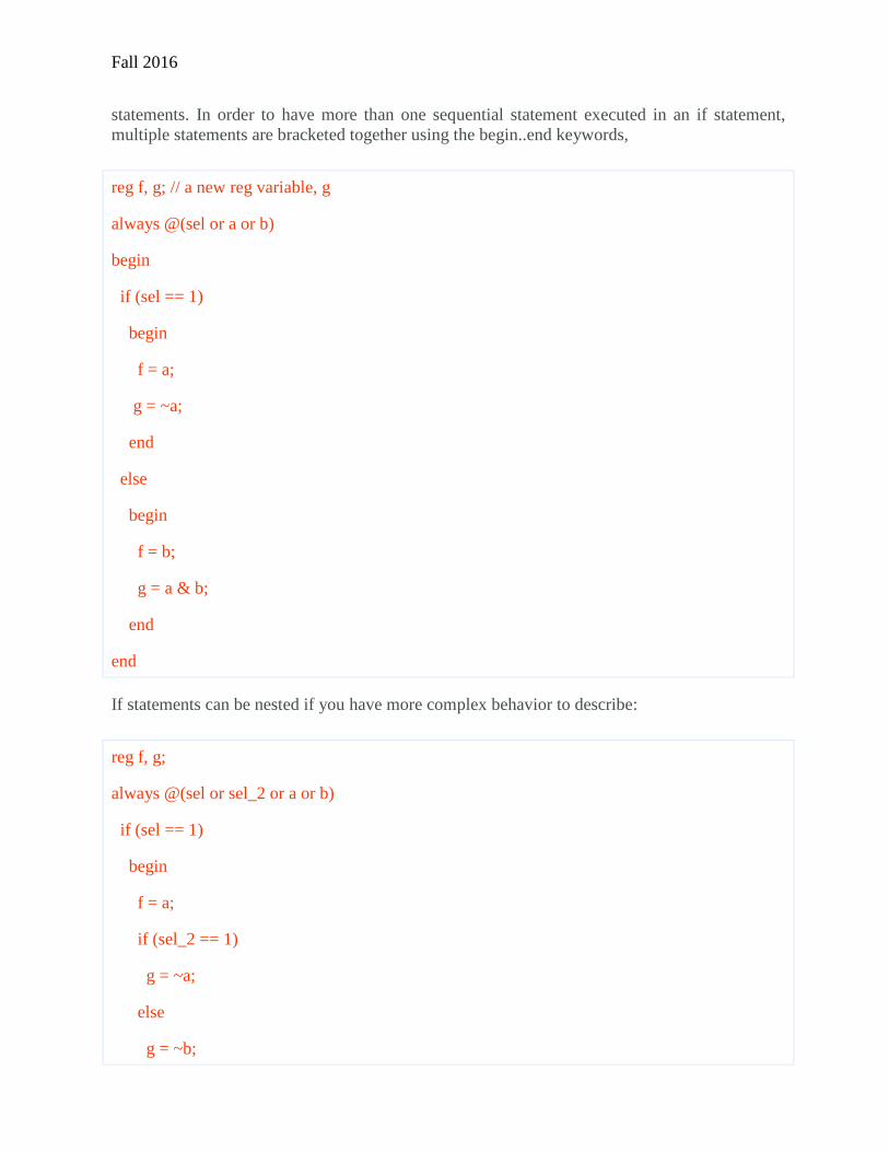
statements. In order to have more than one sequential statement executed in an if statement, multiple statements are bracketed together using the begin..end keywords,
reg f, g; // a new reg variable, g
always @(sel or a or b)
begin
if (sel == 1)
begin
f = a;
g = ~a;
end
else
begin
f = b;
g = a & b;
end
end
If statements can be nested if you have more complex behavior to describe:
reg f, g;
always @(sel or sel_2 or a or b)
if (sel == 1)
begin
f = a;
if (sel_2 == 1)
g = ~a;
else
g = ~b;
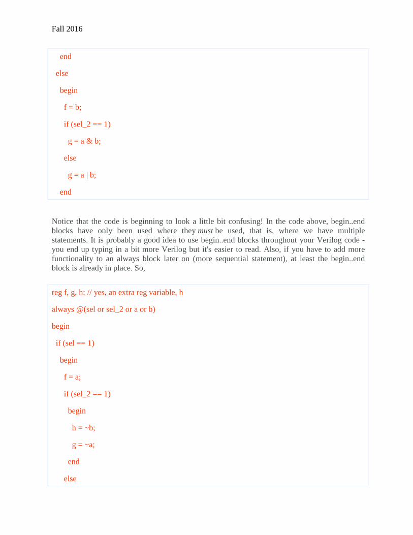
Fall 2016
end
else
begin
f = b;
if (sel_2 == 1)
g = a & b;
else
g = a | b;
end
Notice that the code is beginning to look a little bit confusing! In the code above, begin..end blocks have only been used where they must be used, that is, where we have multiple statements. It is probably a good idea to use begin..end blocks throughout your Verilog code - you end up typing in a bit more Verilog but it's easier to read. Also, if you have to add more functionality to an always block later on (more sequential statement), at least the begin..end block is already in place. So,
reg f, g, h; // yes, an extra reg variable, h
always @(sel or sel_2 or a or b)
begin
if (sel == 1)
begin
f = a;
if (sel_2 == 1)
begin
h = ~b;
g = ~a;
end
else
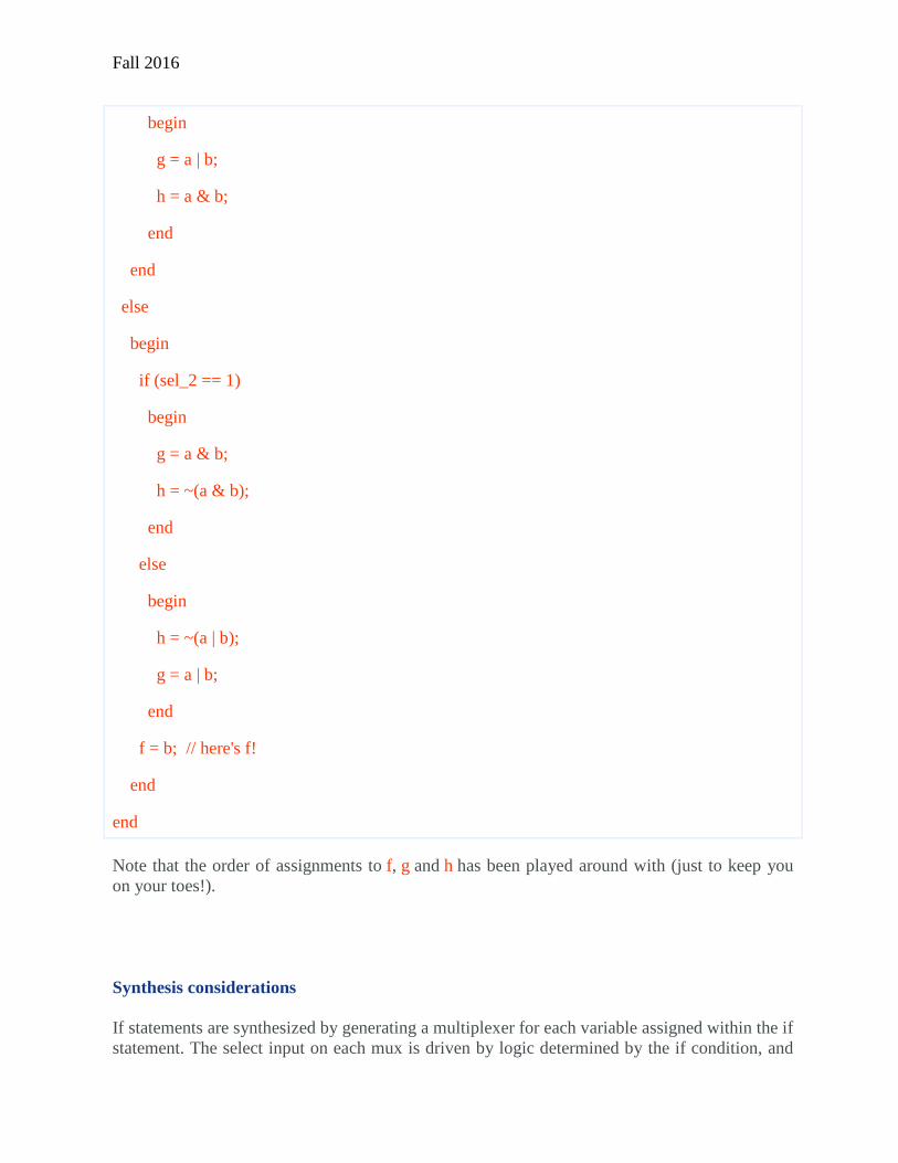
Fall 2016
begin
g = a | b;
h = a & b;
end
end
else
begin
if (sel_2 == 1)
begin
g = a & b;
h = ~(a & b);
end
else
begin
h = ~(a | b);
g = a | b;
end
f = b; // here's f!
end
end
Note that the order of assignments to f, g and h has been played around with (just to keep you on your toes!). Synthesis considerations If statements are synthesized by generating a multiplexer for each variable assigned within the if statement. The select input on each mux is driven by logic determined by the if condition, and
Fall 2016
the data inputs are determined by the expressions on the right hand sides of the assignments. During subsequent optimization by a synthesis tool, the multiplexer architecture may be changed to a structure using and-or-invert gates as surrounding functionality such as the a & b and the ~a can be merged into complex and-or-invert gates to yield a more compact hardware implementation. Synthesizing Latches In the last section, if statements were used to describe simple combinational logic circuits. Synthesizing the Verilog code produced multiplexing circuits, although the exact implementation depends upon the synthesis tool used and the target architecture of the device. As well as enabling the creation of multiplexers, if statements can also be used to implement tristate buffers and transparent latches. In this article we will look at how transparent latches are synthesized from if statements and how to avoid the inadvertent creation of latches when you meant to create combinational logic circuits from Verilog code containing if statements. If Statements In the processes that have been coded up so far, if-else statements rather than simple if statements have been used. Let's use a simple if statement rather than an if-else statement in an example you have already seen:
reg f;
always @ (sel or a or b)
begin : if_else
if (sel == 1)
f = a;
else
f = b;
end
becomes...
reg f;
always @ (sel or a or b)
Fall 2016
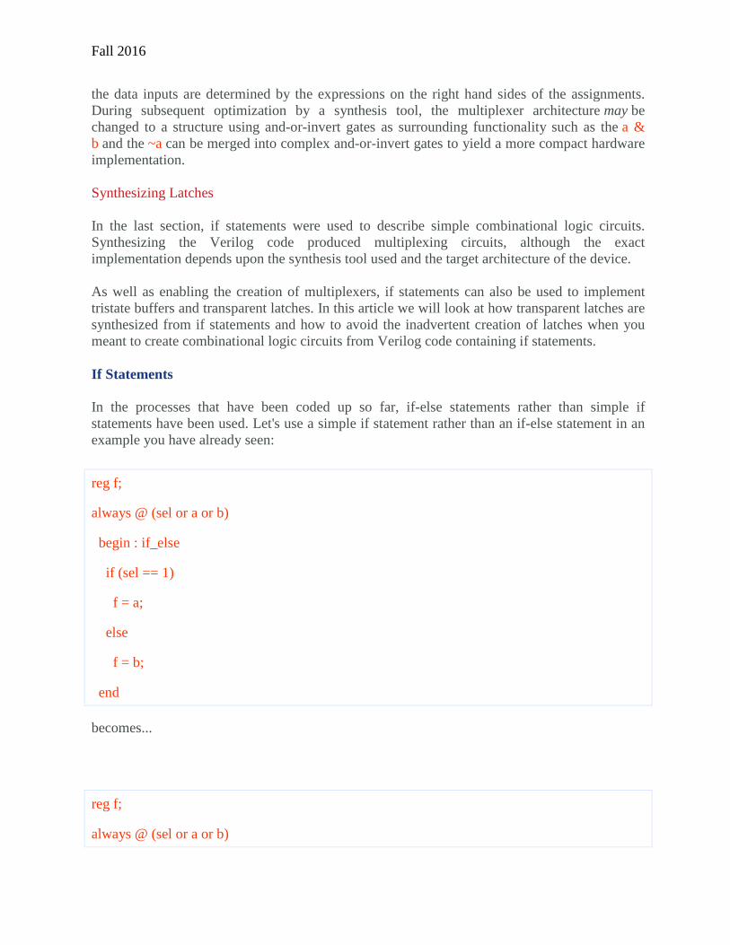
begin : pure_if
f = b;
if (sel == 1)
f = a;
end
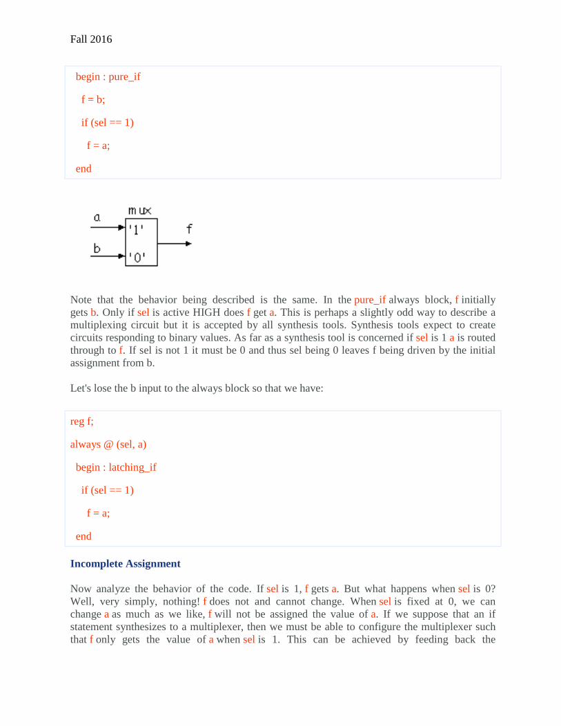
Note that the behavior being described is the same. In the pure_if always block, f initially gets b. Only if sel is active HIGH does f get a. This is perhaps a slightly odd way to describe a multiplexing circuit but it is accepted by all synthesis tools. Synthesis tools expect to create circuits responding to binary values. As far as a synthesis tool is concerned if sel is 1 a is routed through to f. If sel is not 1 it must be 0 and thus sel being 0 leaves f being driven by the initial assignment from b. Let's lose the b input to the always block so that we have:
reg f;
always @ (sel, a)
begin : latching_if
if (sel == 1)
f = a;
end
Incomplete Assignment Now analyze the behavior of the code. If sel is 1, f gets a. But what happens when sel is 0? Well, very simply, nothing! f does not and cannot change. When sel is fixed at 0, we can change a as much as we like, f will not be assigned the value of a. If we suppose that an if statement synthesizes to a multiplexer, then we must be able to configure the multiplexer such that f only gets the value of a when sel is 1. This can be achieved by feeding back the
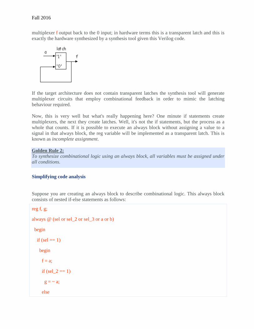
Fall 2016
multiplexer f output back to the 0 input; in hardware terms this is a transparent latch and this is exactly the hardware synthesized by a synthesis tool given this Verilog code.
If the target architecture does not contain transparent latches the synthesis tool will generate multiplexer circuits that employ combinational feedback in order to mimic the latching behaviour required. Now, this is very well but what's really happening here? One minute if statements create multiplexers, the next they create latches. Well, it's not the if statements, but the process as a whole that counts. If it is possible to execute an always block without assigning a value to a signal in that always block, the reg variable will be implemented as a transparent latch. This is known as incomplete assignment. Golden Rule 2: To synthesize combinational logic using an always block, all variables must be assigned under all conditions.
Simplifying code analysis Suppose you are creating an always block to describe combinational logic. This always block consists of nested if-else statements as follows:
reg f, g;
always @ (sel or sel_2 or sel_3 or a or b)
begin
if (sel == 1)
begin
f = a;
if (sel_2 == 1)
g = ~ a;
else
Fall 2016
begin
g = ~ b;
if (sel_3 == 1)
g = a ^ b;
end
end
else
begin
if (sel_2 == 1)
g = a & b;
else
if (sel_3 == 1)
g = ~(a & b);
// oops! no else
// else
// g = ...
f = b;
end
end
Will you get transparent latches on the f and g outputs? Not easy is it? If you look carefully you will see that in fact, g is latched when sel is 0, sel_2 is 0 and sel_3 is 0. The ‘oops!' comment should help you to see where the complete assignment is NOT made. Default Assignment Fortunately, it is possible to save yourself the bother of scouring through the always block code to locate possible incomplete assignments by setting variables to default values at the start of the always block. Using this approach, you may get undesired functionality if you have missed out an assignment (which should be easy to fix) as opposed to unwanted transparent latches. For our current example,
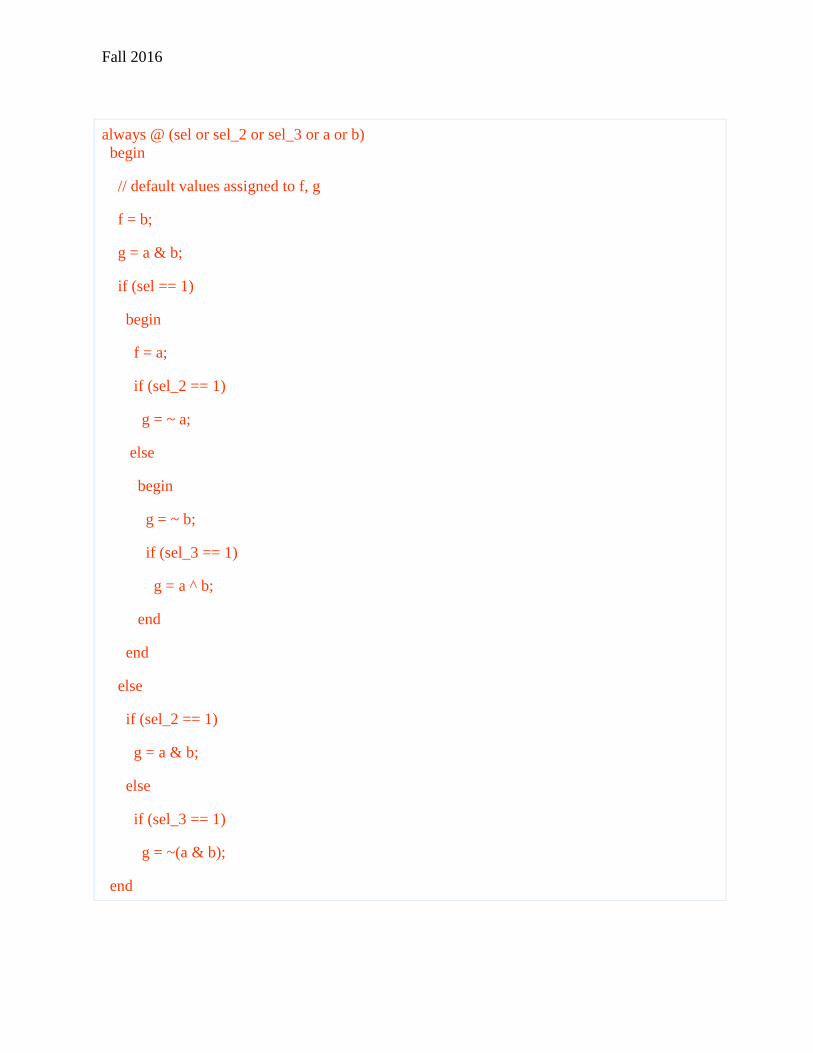
Fall 2016
always @ (sel or sel_2 or sel_3 or a or b) begin
// default values assigned to f, g
f = b;
g = a & b;
if (sel == 1)
begin
f = a;
if (sel_2 == 1)
g = ~ a;
else
begin
g = ~ b;
if (sel_3 == 1)
g = a ^ b;
end
end
else
if (sel_2 == 1)
g = a & b;
else
if (sel_3 == 1)
g = ~(a & b);
end

Fall 2016
Reference:
1. http://www.doulos.com/knowhow/verilog_designers_guide/