Embed Size (px)
Citation preview

Effect of Preconditioning and
Soldering on Failures of Chip
Tantalum Capacitors
NEPP task 2014
Alexander Teverovsky
Parts, Packaging, and Assembly Technologies Office, Code 562, GSFC/ ASRC S&D [email protected]
NASA Electronic Parts and Packaging (NEPP) Program
Deliverable to NASA Electronic Parts and Packaging (NEPP) Program to be published on nepp.nasa.gov. 1

List of Acronyms and Symbols
AC alternating current MSL moisture sensitivity level
C capacitance PI polyimide
CCS constant current stress RH relative humidity
CTE coefficient of thermal expansion S&Q screening and qualification
DCL direct current leakage SBDS simulated breakdown screen
DF dissipation factor SCT surge current test
EDS energy dispersive analysis SEM scanning electron microscopy
EM electrical measurements STD standard deviation
ESR equivalent series resistance T temperature
HV high voltage TSD terminal solder dip
IR infra red VBR breakdown voltage
LDC lot date code VR rated voltage
MC molding compound X-sect cross-section
Deliverable to NASA Electronic Parts and Packaging (NEPP) Program to be published on nepp.nasa.gov. 2

Abstract
Soldering of molded case tantalum capacitors can result in damage to
Ta2O5 dielectric and first turn-on failures due to thermo-mechanical
stresses caused by CTE mismatch between materials used in the
capacitors. It is also known that presence of moisture might cause damage
to plastic cases due to the pop-corning effect. However, there are only
scarce literature data on the effect of moisture content on the probability of
post-soldering electrical failures. In this work, that is based on a case
history, different groups of similar types of CWR tantalum capacitors from
two lots were prepared for soldering by bake, moisture saturation, and long-
term storage at room conditions. Results of the testing showed that both
factors: initial quality of the lot, and preconditioning affect the probability of
failures. Baking before soldering was shown to be effective to prevent
failures even in lots susceptible to pop-corning damage. Mechanism of
failures is discussed and recommendations for pre-soldering bake are
suggested based on analysis of moisture characteristics of materials used
in the capacitors’ design.
Deliverable to NASA Electronic Parts and Packaging (NEPP) Program to be published on nepp.nasa.gov. 3

Outline
4
Background. History case.
Literature data.
Test plan.
Test results. Initial characterization of the lots.
Effect of preconditioning on AC and DC characteristics.
Solder reflow profile.
Effect of preconditioning on post-soldering characteristics and
failures.
Effect of the terminal solder dip testing.
Discussions. Moisture in solid chip tantalum capacitors.
Mechanism of failures.
Summary and recommendations.
Deliverable to NASA Electronic Parts and Packaging (NEPP) Program to be published on nepp.nasa.gov.

5
Background
Both, an engineering and a flight units failed within
a few seconds after powering on for the first time.
The failure was due to CWR29 10uF 35V capacitors used in the 15V
power line. Maximum current in the line was limited to 1 A.
After capacitors were replaced, the unit operated normally.
Out of 20 LDC1307 capacitors from Mfr.A used in the unit, 10 failed
catastrophically.
Out of 18 similar capacitors from Mfr.B that were also used in this unit,
none failed short circuit.
Analysis of leakage currents after desoldering showed that a large
proportion of capacitors from both lots had substantially degraded
characteristics (70% from Mfr.A and 40% from Mfr.B).
Out of two capacitors from Mfr.A that were also used on the board, but
inactivated during the first power on, one sample failed short circuit at
R ~ 6.8 kOhm.
Reflow soldering temperature profile was close to the one recommended
for tantalum capacitors by manufacturers.
Deliverable to NASA Electronic Parts and Packaging (NEPP) Program to be published on nepp.nasa.gov.

6
Background, Cont’d
A review of production test documents did not reveal any anomaly with LDC1307.
A review of the system design and test condition ruled out the possibility of
voltage overshooting of the parts during turn-on of the unit.
Visual and X-ray analysis of failed capacitors did not show any defects.
Stripping of molding compound by Mfr.A and GSFC lab showed that all
capacitors with LDC1307 had damage at the anode shoulder. IR images of 6
failed capacitors confirmed that the location of damage is at the anode shoulder.
This, as well as comparison with the other lot used in
the unit, lead to a suspicion that the problem is
lot-related.
Another possibility that is usually considered when
first turn-on failures happen, is that the capacitors
were damaged during soldering.
LDC1307 was marked MSL 1, which means unlimited
floor life and no need for bake before soldering.
The purpose of this study is to evaluate the
effect of preconditioning and lot-t-lot variations
on the probability of post-soldering failures.
Top view (anode shoulder) of a
stripped capacitor showing
damaged sites
Deliverable to NASA Electronic Parts and Packaging (NEPP) Program to be published on nepp.nasa.gov.

7
Literature Data: Effect of Soldering It is well known that molded case tantalum capacitors can be damaged
during soldering and related to damaging first power-on failures are one of
the major reasons for voltage derating [1].
The effect is mostly attributed to CTE mismatch between molding compound
and tantalum slug [1, 2] and was directly demonstrated in [3].
Tantalum chip capacitors are the only parts that require 100% reflow
simulation to reduce soldering-related failures. Per MIL-PRF-55365 reflow
conditioning requires one exposure to 230 oC for 5 sec.
Different lots might have different susceptibility to soldering-related failures
[4] and large-size capacitors are assumed to have a higher risk of being
damaged [5].
Mechanical stresses associated with reflow soldering can reduce breakdown
voltage and increase the probability of failures in humid environments [6].
Manual soldering might be especially detrimental: stresses caused by
touching a part with a soldering iron can cause more damage than
temperature gradients [7].
A terminal solder dip test was recommended to assess the robustness of
tantalum capacitors to manual soldering [8].
Deliverable to NASA Electronic Parts and Packaging (NEPP) Program to be published on nepp.nasa.gov.

Literature Data:
Pop-Corning
8
Direct measurements of deformation of plastic
packages during soldering simulation showed the
presence of pop-corning in tantalum capacitors.
Baking before soldering was recommended to
eliminate possible problems [4]. Degradation of
VBR after thermal cycling was observed in 4 out
of 6 MIL and 2 out of 10 commercial lots
Pop-corning-related failures of chip tantalum capacitors were reported by R.
Dobson from Raytheon [9]. The failure mechanism was attributed to silver
migration that happen in humid environments prior to soldering.
Occasionally, cracks in the packages are observed on parts before soldering [10].
An unusual failure in BGA components that are adjacent to chip tantalum
capacitors was reported in [11]. The failures were attributed to moisture that
penetrated and was trapped in capacitors. During the board assembly reflow
process the moisture heated up, built up the pressure resulting in cracking of the
case. Moisture from the caps was out-gassing through the cracks, blowing the
solder, and causing shorts or opens between BGA balls.
15 uF 50 V
0
50
100
150
200
250
0 10 20 30time, min
tem
pera
ture
, o
C
-10
0
10
20
30
40
50
60
70
80
defo
rmati
on
, u
m
cycle 1 T
cycle 2 T
cycle 1 d
cycle 2 d
Deformation of Tantalum Capacitors
During Reflow Soldering Simulation [4]
Spike
caused by
moisture
Deliverable to NASA Electronic Parts and Packaging (NEPP) Program to be published on nepp.nasa.gov.

Literature Data: Effect of Preconditioning
9
In a recent study by W. Winkel and E. Rich [12] from Raytheon, the impact that
moisture and exposure to solder reflow have upon 35V CWR11 capacitors was
studied. 850 capacitors were tested by different profiles varying by bake-out,
humidity, and aqueous cleaning. Results of the testing showed:
No failures for parts soldered after bake-out at 40ºC for 72 hours.
Simulation of the uncontrolled storage profile (preconditioning at 48 hr, 30°C/91%RH)
before soldering and repeat soldering after aqueous wash showed that all parts remained
within the specification limits. All parts had breakdown voltages exceeding VR; however,
~2% of capacitors in each group had reduced breakdown voltages compared to the initial
distributions measured by SBDS.
Exposure to 3 cycles of soldering also reduced VBR measured by SBDS in ~5% of parts.
The study indicates that the presence of moisture might increase the probability of post-
soldering failures.
The pop-corning can be initiated by liquid cleaning of PWBs. Warm parts might
suck liquid in through gaps in the package. The liquid will be trapped in the case
after cooling and cause its rupture when another side of the board is soldered.
Application of a moisture barrier between anode and silver ink reduced
substantially the probability of pop-corning failures especially in high-humidity
countries that was explained by decreasing silver migration to the dielectric [13].
Deliverable to NASA Electronic Parts and Packaging (NEPP) Program to be published on nepp.nasa.gov.

MSL: Manufacturers’ Approach
10
According to the product catalogs, most MIL-spec tantalum capacitors have
MSL 1, which means unlimited floor life at T ≤ 30 °C and RH ≤ 85%. However,
there is no established procedure for testing after soldering, and it is not clear
how the level of MSL was verified.
Vishay: The molded series devices meet MSL 1, are not considered moisture sensitive
and are not stored or shipped in moisture protective packaging.
www.vishay.com/doc?40135 Some commercial molded case and coated devices are
considered MSL 2a or 3 http://www.vishay.com/docs/40110/faq.pdf
KEMET: all MIL parts have MSL 1. For commercial product, the necessity of moisture
bags should be indicated in the ordering information. http://www.kemet.com/Lists/ProductCatalog/Attachments/226/KEM_TC105_CWR.pdf
AVX Biddeford has begun shipping all COTS+, military, space level, and medical grade
surface mount tantalum capacitors in moisture resistant bags as part of an upgrade to
best practice. Biddeford product that is considered to be MSL 3 includes TBMs, TCPs,
TBJ V, U and E case, and TAZ V and X case sizes. The remainder of tantalum
capacitors are rated MSL 1 (per J STD 020D). http://www.avx.com/docs/masterpubs/highreltant.pdf
Per JESD22-A113 “Preconditioning of Nonhermetic Surface Mount Devices
Prior to Reliability Testing”, verification of MSL 1 requires soaking at 85 °C, 85%
RH for 168 hours. However, a detailed plan for the initial and post-reflow
testing should be developed for each device based on its specifics.
MSL testing for tantalum capacitors is not specified.
Deliverable to NASA Electronic Parts and Packaging (NEPP) Program to be published on nepp.nasa.gov.

Part Types and Preliminary Evaluation
11
Parts. 80 samples of CWR29 10uF 35V, LDC1307 (failed on MCE board).
80 samples of CWR09 10uF 35V, LDC1338 (reference parts from the same
manufacturer).
Preconditioning. Gr.I - without preconditioning (use “as is”) for manual soldering simulation;
Gr.II - without preconditioning, “as is”, for reflow soldering;
Gr.III - soldered after moisture soak with Gr.IV and bake at 125 °C for 15 hr;
Gr.IV - soldered after moisture soak at 85 °C, 85%, RH, 100hr.
Both lots were soldered onto PI PWBs at the same process, went
together through the same preconditioning and tests.
All parts passed incoming visual inspection and electrical
measurements.
Gross leak testing without pressurization was performed on 40 CWR29
capacitors. One sample appeared to have a few small bubbles
emitting from the corner.
Deliverable to NASA Electronic Parts and Packaging (NEPP) Program to be published on nepp.nasa.gov.
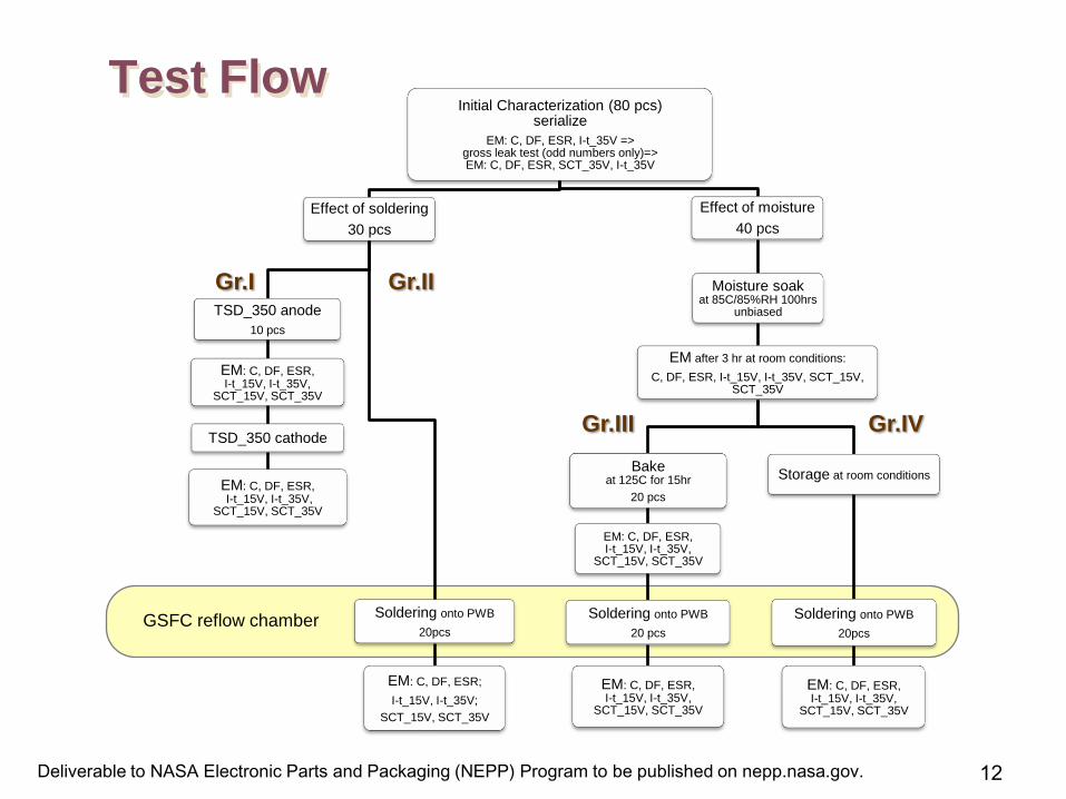
Test Flow
12
Initial Characterization (80 pcs) serialize
EM: C, DF, ESR, I-t_35V => gross leak test (odd numbers only)=> EM: C, DF, ESR, SCT_35V, I-t_35V
Effect of soldering
30 pcs
TSD_350 anode
10 pcs
EM: C, DF, ESR, I-t_15V, I-t_35V,
SCT_15V, SCT_35V
TSD_350 cathode
EM: C, DF, ESR, I-t_15V, I-t_35V,
SCT_15V, SCT_35V
Soldering onto PWB
20pcs
EM: C, DF, ESR;
I-t_15V, I-t_35V;
SCT_15V, SCT_35V
Effect of moisture
40 pcs
Moisture soak at 85C/85%RH 100hrs
unbiased
EM after 3 hr at room conditions:
C, DF, ESR, I-t_15V, I-t_35V, SCT_15V, SCT_35V
Bake at 125C for 15hr
20 pcs
EM: C, DF, ESR, I-t_15V, I-t_35V,
SCT_15V, SCT_35V
Soldering onto PWB
20 pcs
EM: C, DF, ESR, I-t_15V, I-t_35V,
SCT_15V, SCT_35V
Storage at room conditions
Soldering onto PWB
20pcs
EM: C, DF, ESR, I-t_15V, I-t_35V,
SCT_15V, SCT_35V
Gr.I Gr.II
Gr.III Gr.IV
GSFC reflow chamber
Deliverable to NASA Electronic Parts and Packaging (NEPP) Program to be published on nepp.nasa.gov.

Initial AC Characteristics
13
All characteristics are well within the
specification limits (DFmax= 8%,
ESRmax= 0.5 Ohm).
DF values are ~ 10 times less than the
specified limit.
Although CWR29 suppose to be a
low-ESR version of CWR09, ESR
values in CWR09 capacitors are ~
50% less than in CWR29.
capacitance, uF
cu
mu
lati
ve
pro
ba
bil
ity
, %
9.0 10.59.3 9.6 9.9 10.21
5
10
50
99
CWR29CWR09
dissipation factor, %
cu
mu
lati
ve
pro
ba
bil
ity
, %
0.40 0.900.50 0.60 0.70 0.801.E-1
5.E-11
5
10
50
100
1.E-1
CWR29
CWR09
ESR, Ohm
cu
mu
lati
ve
pro
ba
bil
ity
, %
0.10 0.250.13 0.16 0.19 0.221.E-1
5.E-11
5
10
50
100
1.E-1
CWR29
CWR09
Deliverable to NASA Electronic Parts and Packaging (NEPP) Program to be published on nepp.nasa.gov.

Surge Current Testing
14
The set-up used resulted in surge currents at a minimal additional impedance
(Reff ~ 0.2 Ohm), which created current spikes that are within the M55365
requirements, but more severe compared to the testing during manufacturing.
To better simulate application conditions, the parts were first tested by 3 cycles
at 15V and then by three cycles at 35V.
The set-up allowed for verifiable and reproducible test conditions.
To confirm that SCT does not damage parts, leakage currents in capacitors
were measured before and after SCT.
1.E-09
1.E-08
1.E-07
1.E-09 1.E-08 1.E-07
DC
L_1000 a
fter
SC
T,
A
DCL_1000 init, A
CWR29 10uF 35V Effect of SCT
30
40
50
60
70
80
68 70 72 74
Isp
_re
peat,
A
Isp_init, A
Reproducibility of SCT
15V
35V
Deliverable to NASA Electronic Parts and Packaging (NEPP) Program to be published on nepp.nasa.gov.

Initial Surge Current Testing
15
All 160 parts passed SCT at 35V that
resulted in current spikes ~75 A.
A good correlation between Isp and ESR
indicates low circuit resistance, Reff ~ 0.29 Ω.
The difference in Isp for CWR29 and the
reference lots corresponds to ESR values.
Difference in the pulse widths corresponds to
the characteristic time of the short circuit
discharge: t ≈ C×ESR.
current spike, A
cu
mu
lati
ve
pro
ba
bil
ity
, %
60 9066 72 78 841.E-1
5.E-11
5
10
50
100
1.E-1
CWR
ref.
spike width, us
cu
mu
lati
ve
pro
ba
bil
ity
, %
3.4 4.43.6 3.8 4.0 4.21.E-1
5.E-11
5
10
50
100
1.E-1
CWR
ref.
60
65
70
75
80
85
90
0.1 0.125 0.15 0.175 0.2 0.225 0.25
Isp
, A
ESR, Ohm
CWR
Ref.
Deliverable to NASA Electronic Parts and Packaging (NEPP) Program to be published on nepp.nasa.gov.

Breakdown Voltages in Capacitors
Desoldered from MCE Boards
16
Intrinsic breakdown voltages in 10uF capacitors from Mfr.A exceed 3×VR and
are above average values typical for capacitors rated to 35V.
All types of capacitors removed from the units had low-voltage tails of VBR
distributions indicating presence of large proportion of defects in the dielectric.
Mf.A capacitors were removed from the failed engineering board (LDC1215) and
both, Mfr.A (LDC1307) and Mfr.C capacitors were removed from the flight board.
Breakdown voltages for these parts as well as for LDC1307 and reference
capacitors were compared to average values for different types of 35V capacitors.
C WR 10uF 35V capacitors
breakdown voltage, V
cu
mu
lati
ve
pro
ba
bil
ity
, %
50 1501001
5
10
50
90
99
Mfr.A
Mfr.A, desoldered
Mfr.C, desoldered
50
70
90
110
130
150
0 10 20 30 40
VB
R_avr,
V
capacitance, uF
Tantalum capacitors rated to 35V
various PN
CWR29 DC1307
CWR29 DC1215
Reference
Mfr.C
Deliverable to NASA Electronic Parts and Packaging (NEPP) Program to be published on nepp.nasa.gov.

Initial DCL Characteristics
17
DCL was measured after 1000 sec to increase the sensitivity to defects.
Majority of parts (~80%) had leakage currents caused by absorption.
All parts were well (more than 100X) within the specification, DCLmax= 4 mA.
Both lots had similar DCL that were below median values for 35V capacitors.
DCL_1000s, A
cu
mu
lati
ve
pro
ba
bil
ity
, %
1.E-9 1.E-71.E-81.E-1
5.E-11
5
10
50
100
1.E-1
CWRref .
y = 8E-10x1.5091
1.E-10
1.E-09
1.E-08
1.E-07
1.E-06
0 10 20 30 40
DC
L_1000s,
A
C, uF
Leakage currents in 35V capacitors
dif ferent PN
CWR29 10uF
REF 10uF
y = 1.73E-06x-8.04E-01
1.E-09
1.E-08
1.E-07
1.E-06
1.E+1 1.E+2 1.E+3
curr
ent@
35V
, A
time, sec
CWR init
y = 1.51E-06x-8.57E-01
1.E-09
1.E-08
1.E-07
1.E-06
1.E+1 1.E+2 1.E+3
curr
ent@
0V
, A
time, sec
CWR init
Polarization
Depolarization
Analysis of initial
characteristics
showed that both lots
had tight distributions
of AC and DC
characteristics
indicative to high-
quality products.
No anomalies were
observed during
surge current testing,
which rules out the
possibility of
screening escapees.
Deliverable to NASA Electronic Parts and Packaging (NEPP) Program to be published on nepp.nasa.gov.

Effect of Preconditioning and Soldering on
AC Characteristics of Gr.III Capacitors
18
All 160 capacitors passed electrical measurements for C, DF, and ESR.
No substantial variations through preconditioning and soldering (ESR raise ~16%).
An increase of capacitance after moisture soak (0.41% for CWR29 and 2.1% for Ref.) is
consistent with literature data [12] and indicates good coverage during MnO2 impregnation.
9.6
9.7
9.8
9.9
10
10.1
10.2
10.3
INIT HUM BAKE SOLD
cap
acitance, uF
CWR DC1307
0
0.2
0.4
0.6
0.8
1
1.2
INIT HUM BAKE SOLD
DF
, %
CWR DC1307
0
0.05
0.1
0.15
0.2
0.25
0.3
0.35
INIT HUM BAKE SOLD
ES
R, O
hm
CWR DC1307
8.9
9
9.1
9.2
9.3
9.4
9.5
9.6
INIT HUM BAKE SOLD
cap
acitance, uF
CWR09 DC1338
0
0.2
0.4
0.6
0.8
1
1.2
INIT HUM BAKE SOLD
DF
, %
CWR09 DC1338
0
0.05
0.1
0.15
0.2
0.25
0.3
0.35
INIT HUM BAKE SOLD
ES
R, O
hm
CWR09 DC1338
Deliverable to NASA Electronic Parts and Packaging (NEPP) Program to be published on nepp.nasa.gov.

Effect of Preconditioning on DCL and
Moisture Uptake
19
Moisture soak and bake did not affect DCL.
Moisture uptake after soak was ~0.067mg for CWR29 and
0.68mg for ref. parts indicating that CWR29 capacitors
were close to saturation.
Baking resulted in mass loss of 0.27mg for CWR29 and
0.23mg for CWR09 (ref.) capacitors suggesting similar
moisture content in “as is” condition.
Moisture uptake in humidity chamber was greater in ref.
parts (0.91 mg vs. 0.33 mg for CWR29). This might
indicate a larger volume of micropores in ref. parts.
C WR29 DC 1307 effect of preconditioning
DCL_1000s, A
cu
mu
lati
ve
pro
ba
bil
ity
, %
1.E-9 1.E-61.E-8 1.E-71.E-1
5.E-11
5
10
50
100
1.E-1
soak at 85C 85%RH 100hr
bake at 125C 15hr
Initial
Ref. DC 1338 effect of preconditioning
DCL_1000s, A
cu
mu
lati
ve
pro
ba
bil
ity
, %
1.E-9 1.E-61.E-8 1.E-71.E-1
5.E-11
5
10
50
100
1.E-1
0.300
0.302
0.304
0.306
0.308
0.310
INIT HUM BAKE
mass, g
CWR
Ref.
Effect of
preconditioning
on average mass
of the parts (error
bars = STD).
Deliverable to NASA Electronic Parts and Packaging (NEPP) Program to be published on nepp.nasa.gov.

Effect of Preconditioning on SCT
20
SCT was repeated after moisture soak and then after bake.
All parts passed the testing and no significant effect on the amplitude and width
of the current spikes was observed.
Some increase in Isp after bake for CWR29 corresponds to ESR variations.
78
80
82
84
78 80 82 84
Isp
_p
ost te
sting
, A
Isp_init, A
Ref. capacitors
hum 35V
bake 35V
3.6
3.65
3.7
3.75
3.8
3.6 3.65 3.7 3.75 3.8
tau_p
ost te
sting
, us
tau_sp_init, us
Ref. capacitors
hum 35V
bake 35V
3.7
3.8
3.9
4
4.1
3.7 3.8 3.9 4 4.1
tau_sp
_p
ost te
sting
, us
tau_sp_init, us
CWR29
hum 35V
bake 35V
66
68
70
72
74
76
66 68 70 72 74 76
Isp
_p
ost te
sting
, A
Isp_init, A
CWR29
hum 35V
bake 35V
Deliverable to NASA Electronic Parts and Packaging (NEPP) Program to be published on nepp.nasa.gov.

Reflow Soldering
21
Temperature profile was selected to comply with manufacturer's
recommendations (AVX: max rate 2 °C/sec, Tmax = 225°C; KEMET: 3 °C/sec,
Tmax = 235°C) and mimic soldering conditions for flight boards.
The chamber is a 10-zone convection reflow oven (Vitronics XPM3). No N2
purging was not used. Solder paste: Nordson, Sn63/Pb37, RMA-P200.
After placing parts on boards with solder, they were “de-moisturized” for two
hours at 93°C before reflow.
No cleaning or touch-up to improve fillets after soldering was used.
To simulate worst case conditions, each board passed through 3 reflow cycles.
Parts were soldered in 2 days after bake and in 4 days after moisture soak.
Optical examinations of soldered capacitors showed no defects.
Deliverable to NASA Electronic Parts and Packaging (NEPP) Program to be published on nepp.nasa.gov.

Effect of Reflow Soldering on AC
Characteristics
22
All post-soldering AC characteristics were
within the specification limits.
Minimal changes occur for parts after
baking.
Parts soaked in moisture had decreased C.
ESR increases as a result of soldering for all
types of preconditioning; however,
degradation was greater in capacitors after
moisture soak.
9
9.2
9.4
9.6
9.8
10
10.2
9 9.2 9.4 9.6 9.8 10 10.2
C_aft
er so
ldering
, u
F
C_before soldering, uF
CWR as is
CWR bake
CWR hum
Ref. as is
Ref. bake
Ref. hum
0.5
0.7
0.9
1.1
1.3
0.5 0.6 0.7 0.8 0.9 1
DF
_aft
er so
ldering
, %
DF_before soldering, %
CWR as is
CWR bake
CWR hum
Ref. as is
Ref . bake
Ref . hum
0.1
0.15
0.2
0.25
0.3
0.35
0.1 0.12 0.14 0.16 0.18 0.2 0.22 0.24 0.26
ES
R_aft
er so
ldering
, O
hm
ESR_before soldering, Ohm
CWR as isCWR bakeCWR humRef. as isRef . bakeRef . hum
Deliverable to NASA Electronic Parts and Packaging (NEPP) Program to be published on nepp.nasa.gov.

Effect of Reflow Soldering on AC
Characteristics, Cont’d
23
No substantial changes in capacitance.
Degradation of DF and ESR is greater for
reference parts for all types of preconditioning.
Parts after baking increase ESR on 10% to
16%, but in the presence of moisture the
increase is 29% to 46%.
characteristic as is hum bake
DC_CWR29, % -0.11 (0.1) -0.07 (0.12) -0.12 (0.06)
DDF_CWR29, % 14.8 (4.9) 23.4 (13.3) 15.2 (6.17)
DESR_CWR29, % 16.8 (7.68) 28.7 (6.03) 10.8 (7.17)
DC_ref, % 0.28 (0.57) 1.15 (0.17) 0.26 (0.31)
DDF_ref, % 22.9 (3.65) 54.1 (8.66) 22.9 (9.6)
DESR_ref, % 18.3 (7.5) 46.3 (8.2) 15.7 (4.5)
Changes in AC characteristics as a result of
soldering compared to the initial values
measured on loose parts
0
10
20
30
40
50
60
70
as is hum bake
DF
de
via
tio
n, %
Effect of soldering
DF_CWR
DF_ref
0
10
20
30
40
50
60
as is hum bake
ES
R d
evia
tio
n, %
Effect of soldering
ESR_CWR
ESR_ref
Deliverable to NASA Electronic Parts and Packaging (NEPP) Program to be published on nepp.nasa.gov.

Failures after Reflow Soldering
24
The probability of post-soldering failures depends on both factors:
preconditioning and lot date code.
Precond./
Test
CWR29, DC1307 CWR09 (Ref.) DC1338
as is Bake Moisture as is Bake Moisture
AC testing 0/20 0/20 0/20 0/20 0/20 0/20
SCT at 15V 2/20 0/20 9/20 0/20 0/20 0/20
SCT at 35V 1/18 0/20 8/11 0/20 0/20 1/20
DCL at 15V 0/17 0/20 0/3 0/20 0/20 0/19
DCL at 35V 1/17 0/20 0/3 0/20 0/20 0/19
Total 20% 0 85% 0 0 5%
One CWR29 part in
“as is” condition failed
after 1 hour of DCL
testing at 35V.
Some SCT failures
resulted in mechanical
damage to the parts;
however, no burning
was observed.
After soldering the parts were tested in the sequence shown in the table.
Out of 11 CWR29 parts that failed at 15V (>1A after 50 msec),
one failed the first SCT cycle, 8 after the second, and 2 after the third cycle. All
nine parts tested at 35V
failed at the first cycle.
Deliverable to NASA Electronic Parts and Packaging (NEPP) Program to be published on nepp.nasa.gov.

SCT Failures After Reflow Soldering
25
No case defects were observed after soldering.
Case cracking and damage occur in 50% of CWR29 capacitors after SCT.
SCT did not cause damage to CWR09 (reference) parts.
Board B was populated with CWR29 capacitors that were preconditioned in
humidity chamber (samples A1-A20) and reference parts (samples B1-B20).
Cracks were observed on the top and at the bottom of the CWR29 capacitors.
Deliverable to NASA Electronic Parts and Packaging (NEPP) Program to be published on nepp.nasa.gov.

Effect of Reflow Soldering on DCL
26
One CWR29 sample from Gr.II (“as is”) failed
after 10 min at 15V and another after 1 hr at 35V.
No difference in distributions of leakage current
for not-failed capacitors with different
preconditioning.
Non-failed CWR29 samples from the group that
was soaked in moisture before soldering had low
leakage currents.
Desoldering of baked capacitors did not change
DCL distributions.
1.E-09
1.E-08
1.E-07
1.E-06
1.E+1 1.E+2 1.E+3 1.E+4 1.E+5
curr
ent,
Atime, sec
CWR 10uF 35V soldered as is
SN54-10m at 15VSN46- 1hr at 35V
1.E-09
1.E-08
1.E-07
1.E-06
1.E+1 1.E+2 1.E+3 1.E+4 1.E+5
curr
ent,
A
time, sec
Ref. soldered after moisture soak
sample had excessive DCL before soldering
Effect of soldering, C WR29
DCL_1000s, A
cu
mu
lati
ve
pro
ba
bil
ity
, %
1.E-9 1.E-71.E-81.E-1
5.E-11
5
10
50
100
1.E-1
virgin
"as is", PWB"bake", PWB"moisture soak", PWB
"bake", desoldered
Effect of soldering, ref. capacitors
DCL_1000s, A
cu
mu
lati
ve
pro
ba
bil
ity
, %
1.E-9 1.E-71.E-81.E-1
5.E-11
5
10
50
100
1.E-1
virgin
"as is", PWB
"bake", PWB
"moisture soak", PWB
"bake", desoldered
Deliverable to NASA Electronic Parts and Packaging (NEPP) Program to be published on nepp.nasa.gov.

Effect of Reflow Soldering on SCT
27
SCT of soldered samples resulted in current spikes of a lesser amplitude
(decrease ~10%) and greater width (increase ~30%).
The result are due to increased ESR, and to using ~4” wires to interconnect
the parts with the set-up that increased inductance of the circuit.
55
60
65
70
75
80
85
66 68 70 72 74 76
Isp
_p
ost te
sting
, A
Isp_init, A
CWR29 DC1307
hum 35V
bake 35V
sold 35V
3.5
4
4.5
5
5.5
3.7 3.8 3.9 4 4.1
tau_sp
_p
ost te
sting
, us
tau_sp_init, us
CWR29 DC1307
hum 35V
bake 35V
sold 35V
55
60
65
70
75
80
85
78 80 82 84
Isp
_p
ost te
sting
, A
Isp_init, A
Ref. capacitors
hum 35V
bake 35V
sold 35V
3.5
4
4.5
5
5.5
3.6 3.65 3.7 3.75 3.8
tau_p
ost te
sting
, us
tau_sp_init, us
Ref. capacitors
hum 35V
bake 35V
sold 35V
Correlation between
current spike
amplitudes measured
initially, after different
preconditioning, and
after soldering
Similar correlation for
current spike width
Deliverable to NASA Electronic Parts and Packaging (NEPP) Program to be published on nepp.nasa.gov.

28
Most failures happened at low voltages after anode-side thermal stress.
Self-healed capacitors have a high risk of repeat failures.
Parts with parametric DCL failures can pass surge current testing.
Results are in agreement with the solder reflow test: soldering-related stresses
affected CWR29 capacitors to a much greater degree than the reference parts.
Test
TSD350
anode side
TSD350
cathode side
CWR29,
DC1307
CWR09 Ref.,
DC1338
CWR29,
DC1307
CWR09 Ref.,
DC1338
AC testing 0*/10 0/10 0/5 0/8
DCL at ≤15V 6/10 0/10 1/5 0/8
DCL at 35V 2/5 0/10 1/5 0/8
SCT at 15V 0/5 0/9** 0/5 0/9
SCT at 35V 0/5 0/8** 0/5 0/9
60% of CWR29 capacitors failed
the anode-side testing, whereas
no reference parts failed.
One CWR29 part had a
substantial increase of DF.
Two CWR29 parts recovered at
higher voltages and passed SCT,
but one failed DCL again after
cathode-side testing.
No failures happened after
cathode side solder dip.
Ten samples from each lot in “as is” condition were stressed by 3 cycles of TSD
testing at a solder temperature of 350 °C, first at anode, and then at cathode sides.
Post-TSD measurements were carried out in the sequence shown in the table.
* DF = 4.4%; ** two samples were not tested by mistake
Deliverable to NASA Electronic Parts and Packaging (NEPP) Program to be published on nepp.nasa.gov.

Effect of TSD350 on AC and DC
Characteristics
29
All AC characteristics were
within the specification.
One CWR29 part increased
DF almost an order of
magnitude (this part had also
large DCL at 1V).
Anode-side TSD practically
did not change ESR;
whereas ESR increased on
11% in CWR and 18% in ref.
capacitors (similar to the
effect of reflow soldering).
Two CWR29 parts failing
DCL at 3V recovered at 15V,
but then failed again at 35V.
No degradation of DCL for
the reference capacitors.
1.E-10
1.E-09
1.E-08
1.E-07
1.E-06
1.E-05
1.E-04
1V 3V 15V 35V
curr
ent,
A
Post anode-TSD350
CWR
Ref.
0.1
0.15
0.2
0.25
0.1 0.15 0.2 0.25
ES
R_TS
D350 a
no
de,
Ohm
ESR_init, Ohm
Effect of TSD_350
CWR anode
ref . anode
CWR cathode
ref . cathode
9
9.5
10
10.5
9 9.5 10 10.5
C_TS
D350 a
no
de, uF
C_init, uF
Effect of TSD_350
CWR anode
ref . anode
CWR cathode
ref . cathode
0.6
0.7
0.8
0.9
1
0.5 0.6 0.7 0.8
DF
_TS
D350 a
no
de, %
DF_init, %
Effect of TSD_350
CWR anode
ref . anode
CWR cathode
ref . cathode
4.5%
Deliverable to NASA Electronic Parts and Packaging (NEPP) Program to be published on nepp.nasa.gov.

Effect of Soldering on Breakdown Voltages
30
Most non-failed parts had intrinsic VBRs.
Tails of the distributions indicate defects in Ta2O5.
There is a trend of increasing the number of
defects after soldering capacitors with greater
moisture content.
Desoldering can cause damage to dielectric.
95% of CWR95 parts failed short circuit, whereas
~50% of the reference parts self-healed after
scintillation breakdown.
Results of
VBR tests
CWR29 CWR09 (Ref.)
“as is” Moist. “as is” Moist.
SCT short
circuit
15
(93.7%)
3
(100%)
9
(45%)
10
(55.6%)
SCT self-
healed
1
(6.3%) 0
11
(55%)
8
(44.4%)
Sample size 16 3 20 18
Median VBR, V 112.7 113.3 116.5 115.2
C WR 10uF 35V DC 1307
breakdown voltage, V
cu
mu
lati
ve
pro
ba
bil
ity
, %
50 1501001
5
10
50
90
99
"moisture soak", PWB
"as is", PWB
"bake", desoldered from PWB"bake", desoldered from PWB
virgin
Reference 10uF 35V capacitors
breakdown voltage, V
cu
mu
lati
ve
pro
ba
bil
ity
, %
50 1501001
5
10
50
90
99
"mloisture soak", PWB
"as is", PWB
"bake", desoldered from PWB
virgin
VBR for “moisture soak” and “as is” capacitors was measured with parts soldered onto PWB.
“Bake, desoldered” parts were desoldered from the PI PWB, manually soldered onto FR4 PWB, and then desoldered again.
Initial SCT failures were also used for calculations of VBR distributions.
Deliverable to NASA Electronic Parts and Packaging (NEPP) Program to be published on nepp.nasa.gov.

IR Images of Capacitors Failed after Reflow
Soldering
31
All tested parts that failed
catastrophically after soldering had
damage at the riser wire shoulder.
Parts that failed after breakdown
testing had damage under the
internal portion of the cathode lead
frame.
SN62 failed SCT, 1.5Ω; SN68 failed SCT, 0.7Ω; SN72 failed SCT, 1.3Ω; SN66 after VBR=113V, 1.3Ω
CWR29 capacitors soldered after moisture soak
CWR29 capacitors soldered in “as is” condition
SN46 failed I-t@35V, 62Ω; SN53 failed SCT, 1.6Ω; SN54 failed SCT, 3.9Ω: SN56 failed SCT, 1.2Ω
CWR09 (Ref.) capacitors after moisture soak
SN56 failed SCT, 3.1Ω; SN60 high DCL, VBR=110V
CWR-25
Deliverable to NASA Electronic Parts and Packaging (NEPP) Program to be published on nepp.nasa.gov.

IR Images of Reflow Soldered Capacitors after
VBR Measurements
32
After breakdown tested CWR29 capacitors had damage at the anode side,
whereas all reference capacitors had damage at the cathode side.
CWR29 capacitors soldered in “as is” condition
SN41, VBR=118V; SN42, VBR=112V SN43, VBR=119V
CWR09 (Ref.) capacitors soldered after moisture soak
SN43, VBR=120V; SN44, VBR=94.7V SN47, VBR=116V
Three CWR29 samples soldered in “as is”
condition and 6 reference capacitors
soldered after moisture soak were examined
after VBR testing.
Top view side view
Top view side view
Typical X-ray view showing location
of internal part of cathode terminal
Deliverable to NASA Electronic Parts and Packaging (NEPP) Program to be published on nepp.nasa.gov.

IR Images of Capacitors after TSD350
33
All parts except for one reference capacitor had damage at the riser wire
shoulder of the anode slug.
Reference capacitor SN1 most likely failed at the anode-side corner of the slug.
SN21 failed SCT, 98.7Ω; SN22 failed SCT, 2.3kΩ; SN23 failed SCT, 5.2kΩ; SN24 high DCL, VBR=50V
CWR29 capacitors
CWR09 (Ref.) capacitors
SN1, failure suspect*, VBR = 113V; SN5, failure suspect*, VBR=115V; SN10, normal, VBR=140V
IR images were taken for 6 CWR29 and
3 reference capacitors after SCT.
* The part was not tested properly by SCT, but passed all following tests.
CWR-23
Ref.-5
Deliverable to NASA Electronic Parts and Packaging (NEPP) Program to be published on nepp.nasa.gov.
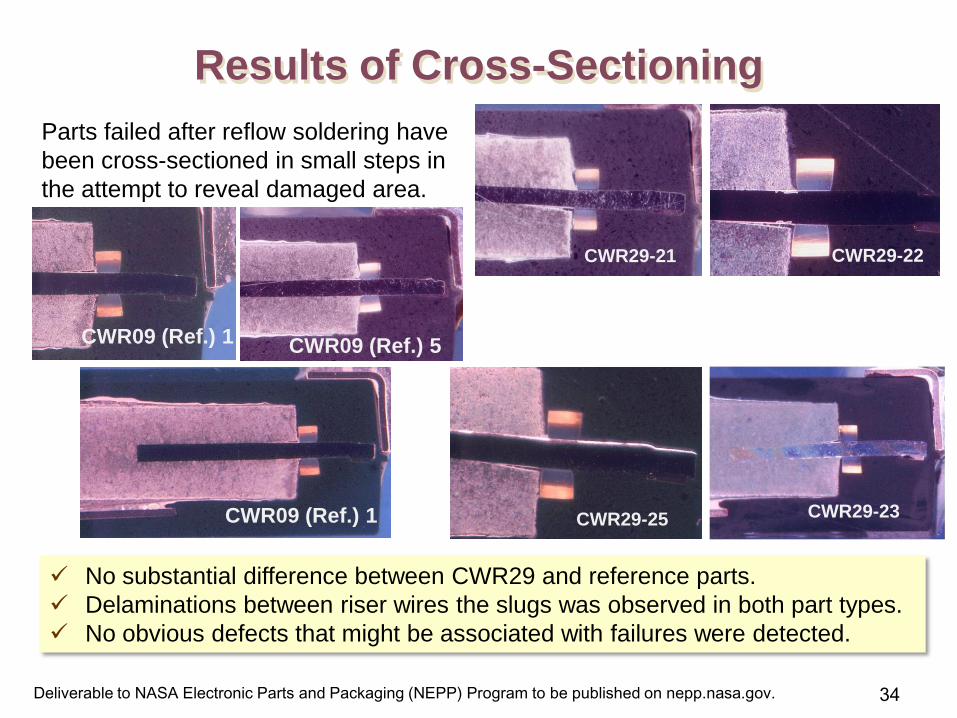
Results of Cross-Sectioning
34
No substantial difference between CWR29 and reference parts.
Delaminations between riser wires the slugs was observed in both part types.
No obvious defects that might be associated with failures were detected.
Parts failed after reflow soldering have
been cross-sectioned in small steps in
the attempt to reveal damaged area.
CWR09 (Ref.) 1
CWR29-22 CWR29-21
CWR29-23 CWR29-25
CWR09 (Ref.) 1 CWR09 (Ref.) 5
Deliverable to NASA Electronic Parts and Packaging (NEPP) Program to be published on nepp.nasa.gov.

SEM Images and X-ray Mapping CWR29
35
No anomalies observed, good coverage of the slug with MnO2 and carbon.
The riser wire shoulder had a thin layers of MnO2 and carbon coatings.
Deliverable to NASA Electronic Parts and Packaging (NEPP) Program to be published on nepp.nasa.gov.

SEM Images and X-ray Mapping for CWR09
(Ref.) Capacitors
36
Results for reference parts were similar to CWR29 capacitors.
SEM and EDS analysis of cross-sectioned samples were not successful in
revealing defects that might be responsible for the difference in behavior of
CWR29 and reference capacitors.
Deliverable to NASA Electronic Parts and Packaging (NEPP) Program to be published on nepp.nasa.gov.

Discussion
37
During manufacturing both lots, CWR29 and CWR09 were solder dipped
to form Sn/Pb finishing on the terminations and stressed by the solder
reflow simulation. However, similar stresses during our testing resulted in
substantial fall-outs.
The difference between solder reflow simulation during screening and
actual soldering conditions is due to the moisture content in the parts:
during manufacturing the amount of moisture in capacitors is minimal,
whereas after a few months of storing the parts at room conditions the
amount of moisture increases substantially.
Post-soldering failures observed in this study happened at voltages below
50% VR, so voltage derating is not a panacea.
To understand the mechanism of pop-corning failures and preventive
measures, we need to analyze moisture characteristics of used materials.
Moisture in chip tantalum capacitors is mostly absorbed in MC and
manganese, and condensed in micropores of the slug and
microcracks/delaminations between different cathode and case materials.
Deliverable to NASA Electronic Parts and Packaging (NEPP) Program to be published on nepp.nasa.gov.

Moisture Diffusion in Tantalum Capacitors
38
The values and activation energies of diffusion processes for epoxy
molding compounds used for tantalum capacitors are similar to
characteristics of molding compounds used for microcircuits [15].
Example of moisture sorption kinetics Moisture diffusion coefficients
Temperature dependence of the diffusion coefficient, D(T), was measured
on samples of molding compounds (MC) using a non-isothermal gravimetric
technique [14].
Similar results can be obtained by analysis of isothermal sorption kinetics.
y = 0.0181e-4.522x
y = 0.0713e-5.158x
1.E-09
1.E-08
1.E-07
1.E-06
1.E-05
2 2.25 2.5 2.75 3 3.25 3.5D
, cm
2/s
1000/T, 1/K
Moisture diffusion coefficients in molding compounds used in Ta capacitors
MG70F-0627
MG33F-0520
0
0.1
0.2
0.3
0.4
0.5
0.6
0.7
0 50 100 150 200 250
mo
istu
re u
pta
ke, %
time, hr
MG70F-0627, sorption at 85C/80% RH
MG70F-0627
MG33F-0520
Deliverable to NASA Electronic Parts and Packaging (NEPP) Program to be published on nepp.nasa.gov.

Bake-out Times for Tantalum Capacitors
39
The bake time corresponds to a time that is
required to release ~ 90% of the absorbed
moisture.
Based on D(T) for molding compounds used
in tantalum capacitors, for case H parts (H =
2.8mm), bake-out times are 1000 hr, (~1.5
month), 200 hr (1.2 wk), 62 hr, and 11 hr at
20°C, 55°C, 85°C, and 125°C respectively.
Note that the bake-out time at 150°C is ~5.5
hr, which is far longer than the preheating
step during soldering (~1 min at 150 °C).
Overnight baking at 125 °C (15 hours)
should be sufficient to remove moisture
from most types of capacitors.
Soldering capacitors within 48 hours after
bake or removal from a dry bag should not
cause pop-corning related failures.
)(1.0)(
2
TD
HT t
Assuming the thickness of molding
compound is ~ 1/3 H, the bake
times can be calculated as [16]:
H is the thickness of the package;
D(T) is the coefficient of moisture diffusion.
1.E+00
1.E+01
1.E+02
1.E+03
0 1 2 3 4
chara
cte
ristic tim
e,
hr
case thickness, mm
Bake-out times for CWR capacitors
20C 55C 85C125C 150C case Ecase F case H
Deliverable to NASA Electronic Parts and Packaging (NEPP) Program to be published on nepp.nasa.gov.

Moisture in Tantalum Capacitors
40
Pores in the slugs comprise from 55% to 60% of the slugs’ volume.
Most part of the pores’ volume is filled with manganese.
Most moisture is absorbed in MC, MnO2, and pores of the anode slug.
Moisture sorption in silver epoxy, ~0.1% [17], is far less than in MC (~0.5%).
Manganese covers the slug and fills the pores.
The volume of pores was determined by calculating the density of slugs used in
different case CWR capacitors and comparing with the density of Ta (16.7 g/cc).
CWR29
case
L,
mm
W,
mm
t,
mm
surface
area,
mm2
slug
volume,
mm3
slug
mass,
g
slug
density,
g/cc
porosity
%
E 2.8 0.6 2.0 16.8 3.3 0.021 6.3 56.1
F 3.3 0.6 2.6 24.5 5.4 0.028 5.3 61.5
G 4.5 2.0 2.0 43.2 17.3 0.113 6.5 54.9
H 4.6 1.6 2.7 48.7 19.9 0.128 6.5 55.2
X 4.5 1.5 4.5 68.4 31.0 0.174 5.6 59.8
Deliverable to NASA Electronic Parts and Packaging (NEPP) Program to be published on nepp.nasa.gov.

Moisture Content
41
The calculated amount of moisture for case H capacitors, ~1.5×10⁻³ g,
corresponds to experimental data (3 to 9)×10-4 g. Most likely, actual amount of
moisture is greater than the one determined by baking.
The amount of moisture condensed in pores of the slug filled with MnO2 is
comparable with the amount of moisture absorbed in MC.
Moisture content was calculated in the following
assumptions: Moisture uptake in MC at 85%RH is ~0.5%.
The thickness of MnO2 layer on the slug is ~ 0.1mm.
MnO2 occupies 50% of the volume of pores.
Moisture uptake in MnO2 at 85%RH is ~2% [18].
volume, mm3 mass, g moisture, g
CWR29
case case slug pores MC MnO2 case MC MnO2 MC MnO2 total
E 16.4 3.4 1.9 11.7 2.6 0.06 0.02 0.01 1.1E-04 2.6E-04 3.8E-04
F 34.1 5.5 3.4 25.8 4.1 0.11 0.05 0.02 2.5E-04 4.1E-04 6.6E-04
G 52.4 17.5 9.6 31.4 9.1 0.18 0.06 0.05 3.0E-04 9.1E-04 1.2E-03
H 77.0 20.0 11.1 51.2 10.4 0.31 0.10 0.05 4.9E-04 1.0E-03 1.5E-03
X 102.7 31.2 18.8 64.3 16.2 0.37 0.12 0.08 6.1E-04 1.6E-03 2.2E-03
0
0.2
0.4
0.6
0.8
0 20 40 60 80 100
dM
/M, %
RH, %
Sorption isotherm at 85 oC
MG70F-0627
MG33F-0520
Deliverable to NASA Electronic Parts and Packaging (NEPP) Program to be published on nepp.nasa.gov.

Failure Mechanism
42
Examples of cracks in the dielectric of 6.8uF 35V
CWR11 capacitors
Molding compound
Ta slug
moisture
MnO2
crack
The following results indicate that
soldering stresses cause local
mechanical damage (fracture of the
dielectric): No substantial variation of AC characteristics.
No degradation of DCL for most of the parts.
Most of failures occurred at low voltages.
Increase of the low-voltage tails in VBR distributions.
In some cases damage can be self-
healed (e.g. by oxidation of Ta, or
increasing resistance of MnO2). This
might improve temporarily
characteristics of the part, but reliability
of such a part is compromised.
During soldering, moisture condensed in cracks, pores, or MnO2
evaporates rapidly creating high local pressure in the sponge-
like structure of Ta anode and increasing delamination between
MC and slug. When this pressure is applied to a mechanically
weak site of the slug, a fracture of Ta2O5 dielectric occurs.
This effect can be defined as internal popcorning.
Schematic of local popcorning that can cause
cracking in Ta2O5 dielectric
Deliverable to NASA Electronic Parts and Packaging (NEPP) Program to be published on nepp.nasa.gov.

Failure Mechanism: Effect of Surge Currents
43
Chip-outs and cracks in the case were not observed after soldering, but occurred
after surge current testing in CWR29 capacitors preconditioned by moisture soak. Based on temperature dependence of moisture diffusion, bake-out tome at 220C is ~ 1 hr, which
exceeds substantially the time of high-temperature exposure during soldering (a few seconds).
This might indicate that case cracking is due to moisture remaining in the parts after soldering and
overheating of the moisture containing MnO2 layers by surge currents.
It is possible that the surge current power overheats MnO2 layer causing
absorbed moisture to evaporate quickly and result in popcorning. The amplitude of surge current spike at 15V is ~ 35A. Considering that DC resistance during spike is
close to ESR, the dissipated power is ~6.1 kW. However, during ~ 3 ms (duration of spikes) only ~ 0.02
J of energy will be generated.
Due to a short duration of the spike, the energy will be generated adiabatically, and mostly in the MnO2
layer on the surface of the slug. At the specific heat capacity of MnO2 53 J/(K*mol) [19], M = 87g/mol,
and the mass ~0.05g, the temperature increase is below 1°C, which is in agreement with [20].
Estimations show that overheating of MnO2 is not the major cause of pop-corning.
Most likely, overheating occurs locally, in a relatively small area where a defect
(crack in Ta2O5 dielectric) has been formed during the solder reflow process.
The case fracture (popcorning) is caused by a local instant heat release that
creates high thermo-mechanical and water vapor stresses in the case.
Deliverable to NASA Electronic Parts and Packaging (NEPP) Program to be published on nepp.nasa.gov.

Failure Mechanism, Cont’d
44
All revealed damage sites were located at the riser wire
shoulder of the slug. Possible reasons for this location: This area is considered most susceptible to soldering-related failures because
of high level of mechanical stresses caused by the CTE mismatch with molding
compound [5]. Moisture-related swelling and shrinking of MC increases the
level of stress substantially [21].
All other surfaces of the slug are “sealed” with silver epoxy that is compressed
to the slug by molding compound.
The riser wire shoulder is covered by a thin layer of MnO2 and is close to a
large volume of MC. This makes delamination between MC and slug in this
area more likely.
The presence of delamination facilitates movements and fracture of weak sites
of the slug.
The vapor flow from the slug along the delamination would create additional
stress to the weak sites at the riser wire shoulder.
The reason why the reference lot is less moisture sensitive
compared to LDC1307 capacitors is not clear. It is possible
that some variations in the manufacturing process (e.g. during
slug formation and sintering, assembly onto lead-frames,
encapsulation with MC, etc.) result in lots with different
proportion of potentially weak sites on the surface of the slug
that are susceptible to damage by internal popcorning.
Example of weak sites on the
surface of CWR11 capacitors
Schematic of popcorning-
induced damage
Deliverable to NASA Electronic Parts and Packaging (NEPP) Program to be published on nepp.nasa.gov.
Summary: Effect of Reflow Soldering
45
The probability of post-soldering failures depends strongly on
preconditioning suggesting an important role of absorbed moisture in post-
soldering failures. No failures occurred in baked capacitors, whereas 85% of
CWR29 and 5% of reference parts that were soaked with moisture failed.
Different lots of chip tantalum capacitors have different susceptibility to
soldering-related failures.
Popcorning in chip tantalum capacitors might result in cracking of the
molding compound and/or in internal damage to the dielectric (internal
popcorning).
The majority of post-soldering failures occurred at low voltages indicating
that voltage derating might not protect against soldering-related failures.
Reflow soldering increases ESR on 11% -16% in baked parts, 29% to 46%
in capacitors with moisture, and on ~18% in capacitors after long-term
storage at room conditions.
Deliverable to NASA Electronic Parts and Packaging (NEPP) Program to be published on nepp.nasa.gov.
Summary: Effect of Environments
46
Moisture soak did not degrade characteristics of capacitors before soldering
suggesting that the presence of moisture is much more dangerous for the
soldering process compared to the post-soldering conditions. Even a relatively small amount of moisture that is absorbed in capacitors stored at
room conditions can result in post-soldering failures (20% for CWR29 capacitors),
but normally, this amount of moisture does not cause failures during operation.
A more dangerous situation might occur if failures are not revealed right after
soldering, but the created damage cause failures with time of operation.
Moisture diffusion and sorption in chip tantalum capacitors has been
characterized and bake-out conditions were determined based on
temperature dependence of moisture diffusion in molding compounds. Although bake-out times decrease with the size of capacitors, to simplify
conditioning process, it is recommended that all parts are baked at 125 °C for 15
hours.
The amounts of moisture absorbed in MC and in MnO2 layers at the surface and in
pores of the slug are similar.
Deliverable to NASA Electronic Parts and Packaging (NEPP) Program to be published on nepp.nasa.gov.

Summary, Mechanism of Failures
47
Post-soldering failures are due to a local mechanical damage to the Ta2O5
dielectric. Soldering-induced damage is a result of thermal-shock-related
mechanical stresses that have been increased by the presence of moisture
due to swelling and shrinkage of MC and via the internal popcorning effect.
All failed capacitors had damage at the riser wire shoulder of the anode slug.
This damage was likely caused by preexisting defects that had not been
detected by screening.
The probability of damage depends on the specific features of the sample
(e.g., irregularities on the surface of the slug). However, the proportion of
samples with high likelihood of being damaged by soldering depends on the
manufacturing lot.
Cracking of molding compound might be due to surge currents during first
power turn-on after soldering capacitors containing moisture.
Increase in ESR after soldering is most likely due to termo-mechanical
stresses that result in delaminations between cathode layers. For baked parts,
the increase is 10% to 16%, but for capacitors soaked in moisture it increases
to 29% to 46%.
Deliverable to NASA Electronic Parts and Packaging (NEPP) Program to be published on nepp.nasa.gov.

Summary: Effect of Manual Soldering
48
Results of terminal solder dip testing are in agreement with the results of
solder reflow test. Most CWR29 capacitors (60%) failed at low voltages, whereas there were no
failures for reference parts.
The results confirmed the effectiveness of the terminal solder dip testing
(TSD350) for evaluation of the susceptibility of tantalum capacitors to damage
by soldering stresses.
All catastrophic failures occurred when the anode terminal was
thermally stressed by touching molten solder at 350 °C. Similar to reflow soldering, all failures were due to damage at the riser wire
shoulder of the slug.
Anode-side stresses did not affect ESR.
Cathode-side stresses increased ESR by 11% to 18%. The result is similar to reflow soldering and is also most likely due to
delaminations between cathode layers.
Deliverable to NASA Electronic Parts and Packaging (NEPP) Program to be published on nepp.nasa.gov.

Summary: Recommendations for
Qualification Testing
49
Soldering simulation tests that are used as a part of screening during
manufacturing are carried out using freshly made capacitors with minimal
amount of moisture and do not simulate soldering conditions for the capacitors
that have been stored in non-dry environments for a long period of time.
Life test during qualification should be carried out after preconditioning per the
relevant MSL and reflow soldering onto PWBs using recommended profiles.
Measurements of AC characteristics through the testing showed that they are
much less sensitive to the presence of defects compared to DCL and VBR. The sensitivity to local defects increases in the sequence: AC tests << DCL < VBR.
Surge current test, as well as 5 min measurements of DCL, C, DF, and ESR are recommended to verify
MSL of tantalum chip capacitors.
Qualification testing to verify MSL 1. Precondition 20 capacitors per JESD22-A113 at 85°C, 85%RH for 168hrs;
Within 4 hrs after removal from humidity chamber, solder the samples using reflow temperature profile
recommended by the manufacturer.
Subject the sample to 3 cycles of solder reflow with 10 min intervals for boards to cool down.
Post-soldering tests should be carried out in the sequence: optical examination at 10X, SCT, AC and
DCL measurements.
No cracking or electrical failures allowed.
Deliverable to NASA Electronic Parts and Packaging (NEPP) Program to be published on nepp.nasa.gov.

Summary: Conditioning before Soldering
onto Flight Boards
50
Parts in dry bags sealed by manufacturers can be used within 48
hours after removing from the bags provided reading of humidity
indicators are acceptable.
All solid chip tantalum capacitors that were not stored in dry
conditions should be baked for 15 hours at 125°C and used within 48
hrs after bake.
After the bake or removal from the sealed bags, if necessary, the
parts can be stored in dry boxes (RH < 10%).
Deliverable to NASA Electronic Parts and Packaging (NEPP) Program to be published on nepp.nasa.gov.

References
51
[1] J. D. Prymak, et al., "Proofing Tantalum Capacitors and Effects on Reliability," in The 26th symposium for
passive components, CARTS Europe'05, Prague, CZ Republic, 2005, pp. 171-178.
[2] J. Marshall and J. Prymak, "Surge step stress testing of tantalum capacitors," in 21st Capacitors and
Resistors Technology Symposium, CARTS'01, 2001, pp. 181-187.
[3] R. Hahn, et al., "Improved SMT Performance of Tantalum Conductive Polymer Capacitors with Very Low
ESR," in The 26th symposium for passive components, CARTS'06, Orlando, FL, 2006, pp. 291-303.
[4] A. Teverovsky, "Effect of Temperature Cycling and Exposure to Extreme Temperatures on Reliability of
Solid Tantalum Capacitors," in CARTS'07, the 27th Symposium for Passive Components, Albuquerque,
NM, 2007, pp. 279-306.
[5] D. M. Edson and J. B. Fortin, "Improving thermal shock resistance of surface mount tantalum capacitors,"
in 14th Capacitors and Resistors Technology Symposium, Jupiter, FL, 1994, pp. 169-176.
[6] J. Virkki, et al., "Testing the effects of reflow on tantalum capacitors," Microelectronics Reliability, vol. 50,
pp. 1650-1653, Sep-Nov 2010.
[7] A. Teverovsky, "Effect of Environmental Stresses on Breakdown Voltages in Chip Tantalum Capacitor.," in
The 28th Symposium for Passive Components, CARTS'09, Jacksonville, FL, 2009, pp. 293-310.
[8] A. Teverovsky, "Terminal Solder Dip Testing for Chip Ceramic and Tantalum Capacitors," in International
Conference on Soldering & Reliability (ICSR) Ontario, Canada, 2012, pp. 163-173.
[9] R. Dobson, "Surface mount solid tantalum capacitor new wear-out mechanism," in CARTS'03, 23rd
Capacitor and Resistor Technology Symposium, Scottsdale, Arizona, 2003, pp. 141-148.
[10] GIDEP alert G2-P-09-01, “CWR09 external body cracks”, 2009 .
[11] D. Amir, "Capacitor induced BGA assembly failures," in SMTA International, 2000. Available:
http://www.smta.org/knowledge/proceedings_abstract.cfm?PROC_ID=539
Deliverable to NASA Electronic Parts and Packaging (NEPP) Program to be published on nepp.nasa.gov.

References, Cont’d
52
[12] W. Winkel and E. Rich, "High Reliability Principles and Verifications in Solid Tantalum Capacitors. End-
User’s Manufacturing Processes," in CARTS International, Santa Clara, CA, 2014.
[13] J. Moore, J. Prymak, and N. Reynolds, "Moisture - An Old and Known Nemesis of Tantalum Caps",
KEMET Tantalum Applications. 2000, Available:
http://www.kemet.com/Lists/TechnicalArticles/Attachments/184/Moisture%20Barrier.pdf
[14] A. Teverovsky, "Moisture Characteristics of Molding Compounds in PEMs", NEPP Report. 2002,
Available: https://nepp.nasa.gov/DocUploads/B9C0B2A1-4C69-4CB5-
94863C560CBB0B19/Moisture%20Characteristics%203-part%20NEPP%20report.doc
[15] A. Teverovsky, "Effect of Moisture on Characteristics of Surface Mount Solid Tantalum Capacitors," in
CARTS'03, 23rd Capacitor and Resistor Technology Symposium, Scottsdale, Arizona, 2003, pp. 96-111.
[16] A. Teverovsky, "Characteristic Times of Moisture Diffusion and Bake-out Conditions for Plastic
Encapsulated Parts", NEPP Report. 2002, Available: http://nepp.nasa.gov/index_nasa.cfm/477/
[17] H. T. Wang and Y. C. Poh, "An analysis on the properties of epoxy based die attach material and
the effect to delamination and wire bondability," in Electronic Manufacturing Technology
Symposium (IEMT), 2008 33rd IEEE/CPMT International, 2008, pp. 1-6.
[18] C.-N. Xu, et al., "Humidity sensors using manganese oxides," Sensors and Actuators B: Chemical, vol. 46,
pp. 87-96, 1998.
[19] K. T. Jacob, A. Kumar, G. Rajitha, et al., "Thermodynamic Data for Mn3O4, Mn2O3 and MnO2," High
Temperature Materials and Processes, vol. 30, pp. pp. 459–472, 2011.
[20] E. K. Reed, "Tantalum chip capacitor reliability in high surge and ripple current applications," in 44th.
Electronic Components and Technology Conference, 1994, pp. 861-868.
[21] A. Teverovsky, "Environmentally Induced Swelling and Shrinkage of Molding Compounds in PEMs,"
GSFC, Greenbelt MD, 2002, Available: https://nepp.nasa.gov
Deliverable to NASA Electronic Parts and Packaging (NEPP) Program to be published on nepp.nasa.gov.