Embed Size (px)
Citation preview

Z. Feng MTU EE5780 Advanced VLSI CAD11.1
EE5780 Advanced VLSI CAD
Lecture 11 SRAM and Yield AnalysisZhuo Feng
Z. Feng MTU EE5780 Advanced VLSI CAD11.2
Outline■ Memory Arrays■ SRAM Architecture
► SRAM Cell► Decoders► Column Circuitry► Multiple Ports
■ Serial Access Memories
Z. Feng MTU EE5780 Advanced VLSI CAD11.3
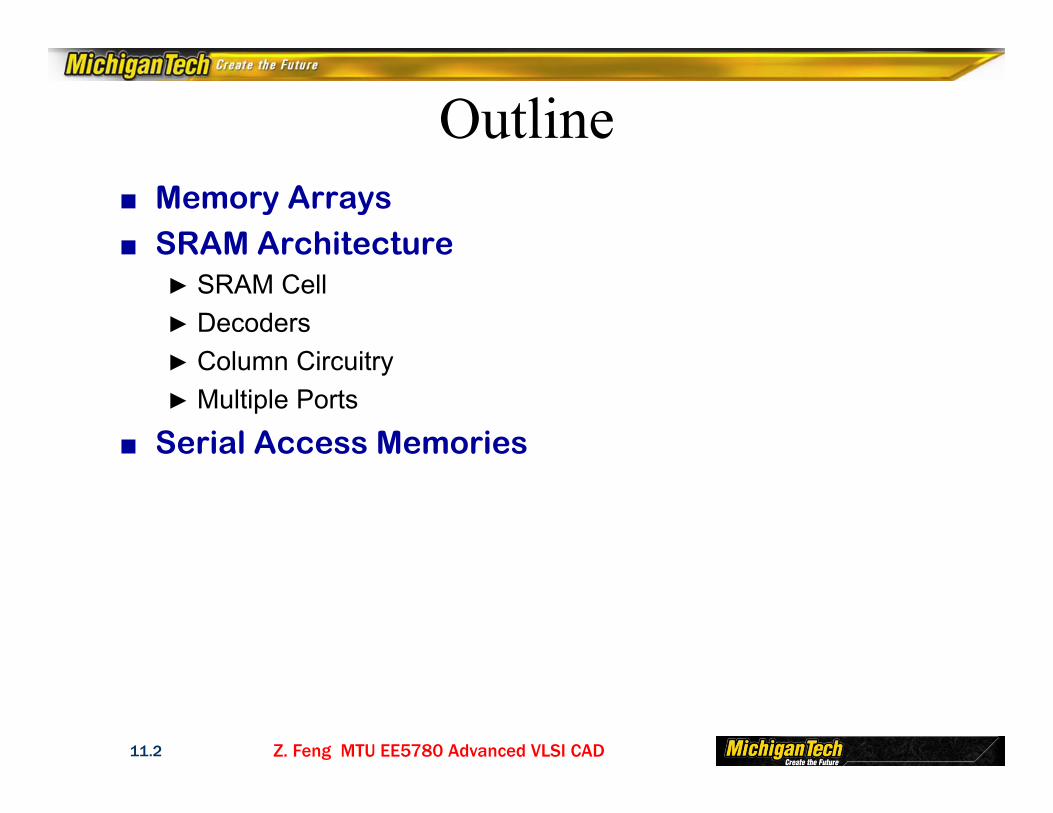
Memory Arrays
Random Access Memory Serial Access Memory Content Addressable Memory(CAM)
Read/Write Memory(RAM)
(Volatile)
Read Only Memory(ROM)
(Nonvolatile)
Static RAM(SRAM)
Dynamic RAM(DRAM)
Shift Registers Queues
First InFirst Out(FIFO)
Last InFirst Out(LIFO)
Serial InParallel Out
(SIPO)
Parallel InSerial Out
(PISO)
Mask ROM ProgrammableROM
(PROM)
ErasableProgrammable
ROM(EPROM)
ElectricallyErasable
ProgrammableROM
(EEPROM)
Flash ROM
Memory Arrays
Z. Feng MTU EE5780 Advanced VLSI CAD11.4
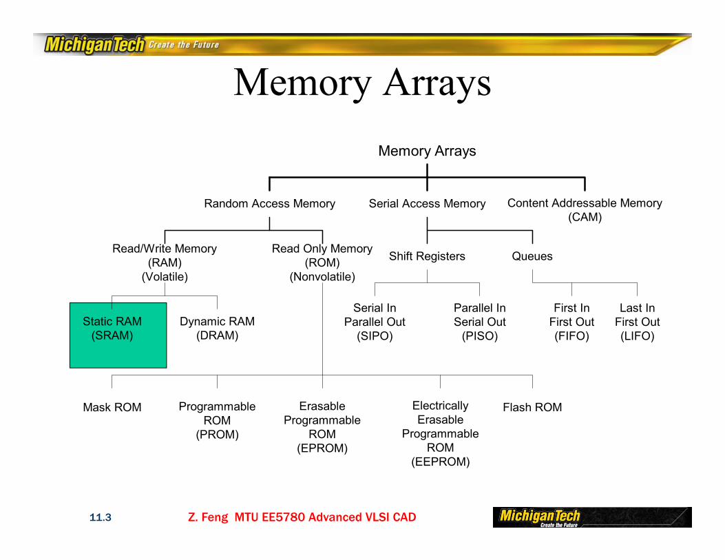
Array Architecture■ 2n words of 2m bits each■ If n >> m, fold by 2k into fewer rows of more columns
■ Good regularity – easy to design■ Very high density if good cells are used
row decoder
columndecoder
n
n-kk
2m bits
columncircuitry
bitline conditioning
memory cells:2n-k rows x2m+k columns
bitlines
wordlines
Z. Feng MTU EE5780 Advanced VLSI CAD11.5
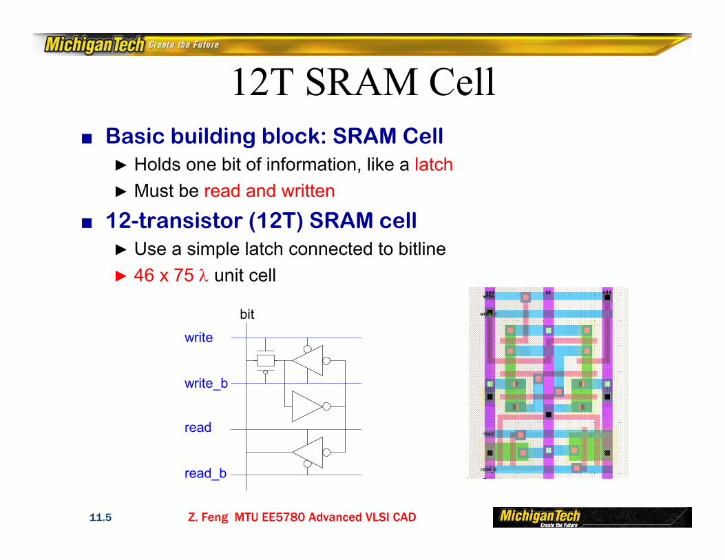
12T SRAM Cell■ Basic building block: SRAM Cell
► Holds one bit of information, like a latch► Must be read and written
■ 12-transistor (12T) SRAM cell► Use a simple latch connected to bitline► 46 x 75 unit cell
bit
write
write_b
read
read_b
Z. Feng MTU EE5780 Advanced VLSI CAD11.6
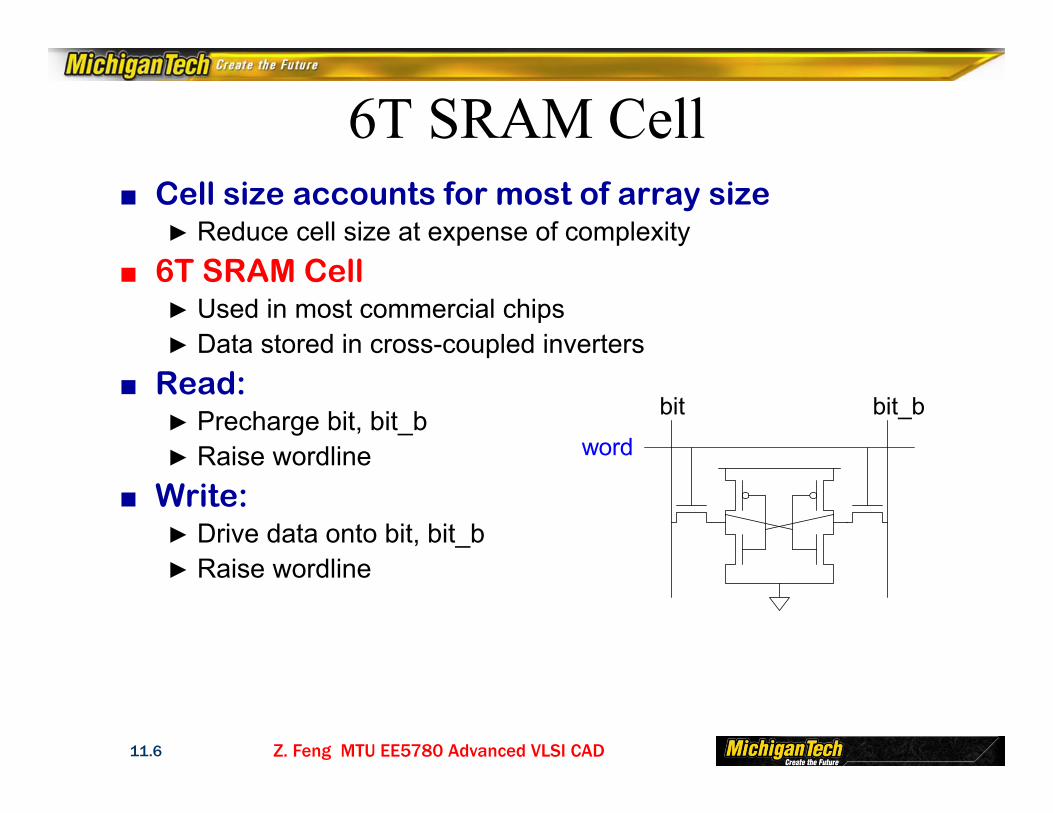
6T SRAM Cell■ Cell size accounts for most of array size
► Reduce cell size at expense of complexity■ 6T SRAM Cell
► Used in most commercial chips► Data stored in cross-coupled inverters
■ Read:► Precharge bit, bit_b► Raise wordline
■ Write:► Drive data onto bit, bit_b► Raise wordline
bit bit_b
word
Z. Feng MTU EE5780 Advanced VLSI CAD11.7
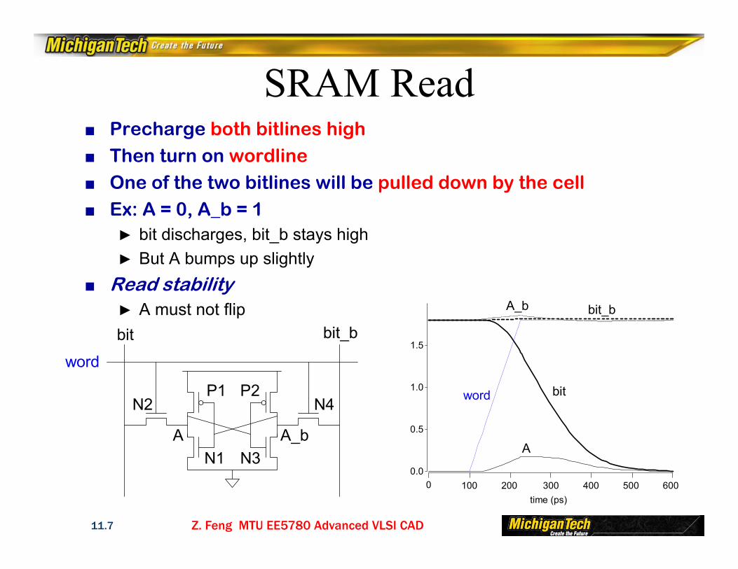
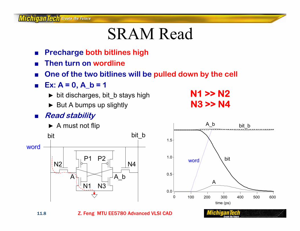
SRAM Read■ Precharge both bitlines high■ Then turn on wordline■ One of the two bitlines will be pulled down by the cell■ Ex: A = 0, A_b = 1
► bit discharges, bit_b stays high► But A bumps up slightly
■ Read stability► A must not flipbit bit_b
N1
N2P1
A
P2
N3
N4
A_b
word
0.0
0.5
1.0
1.5
0 100 200 300 400 500 600time (ps)
word bit
A
A_b bit_b
Z. Feng MTU EE5780 Advanced VLSI CAD11.8
SRAM Read■ Precharge both bitlines high■ Then turn on wordline■ One of the two bitlines will be pulled down by the cell■ Ex: A = 0, A_b = 1
► bit discharges, bit_b stays high► But A bumps up slightly
■ Read stability► A must not flipbit bit_b
N1
N2P1
A
P2
N3
N4
A_b
word
0.0
0.5
1.0
1.5
0 100 200 300 400 500 600time (ps)
word bit
A
A_b bit_b
N1 >> N2N3 >> N4
Z. Feng MTU EE5780 Advanced VLSI CAD11.9
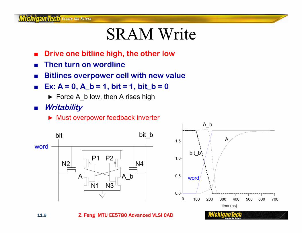
SRAM Write■ Drive one bitline high, the other low■ Then turn on wordline■ Bitlines overpower cell with new value■ Ex: A = 0, A_b = 1, bit = 1, bit_b = 0
► Force A_b low, then A rises high■ Writability
► Must overpower feedback inverter
time (ps)
word
A
A_b
bit_b
0.0
0.5
1.0
1.5
0 100 200 300 400 500 600 700
bit bit_b
N1
N2P1
A
P2
N3
N4
A_b
word
Z. Feng MTU EE5780 Advanced VLSI CAD11.10
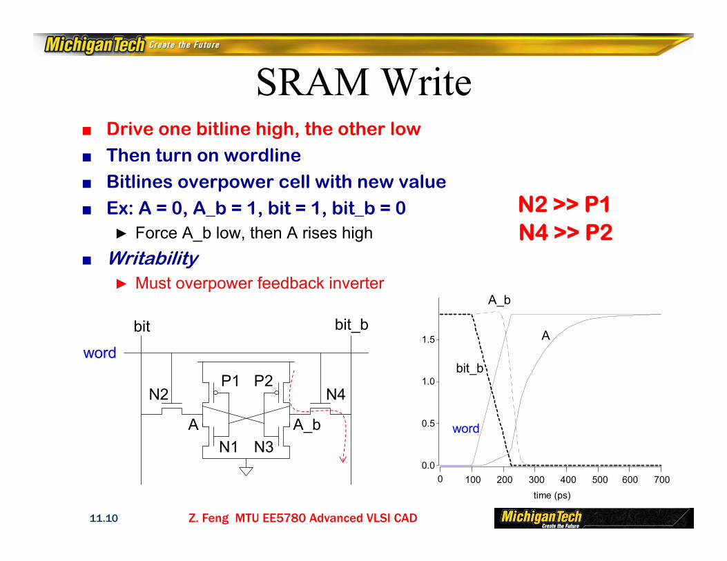
SRAM Write■ Drive one bitline high, the other low■ Then turn on wordline■ Bitlines overpower cell with new value■ Ex: A = 0, A_b = 1, bit = 1, bit_b = 0
► Force A_b low, then A rises high■ Writability
► Must overpower feedback inverter
time (ps)
word
A
A_b
bit_b
0.0
0.5
1.0
1.5
0 100 200 300 400 500 600 700
bit bit_b
N1
N2P1
A
P2
N3
N4
A_b
word
N2 >> P1N4 >> P2
Z. Feng MTU EE5780 Advanced VLSI CAD11.11
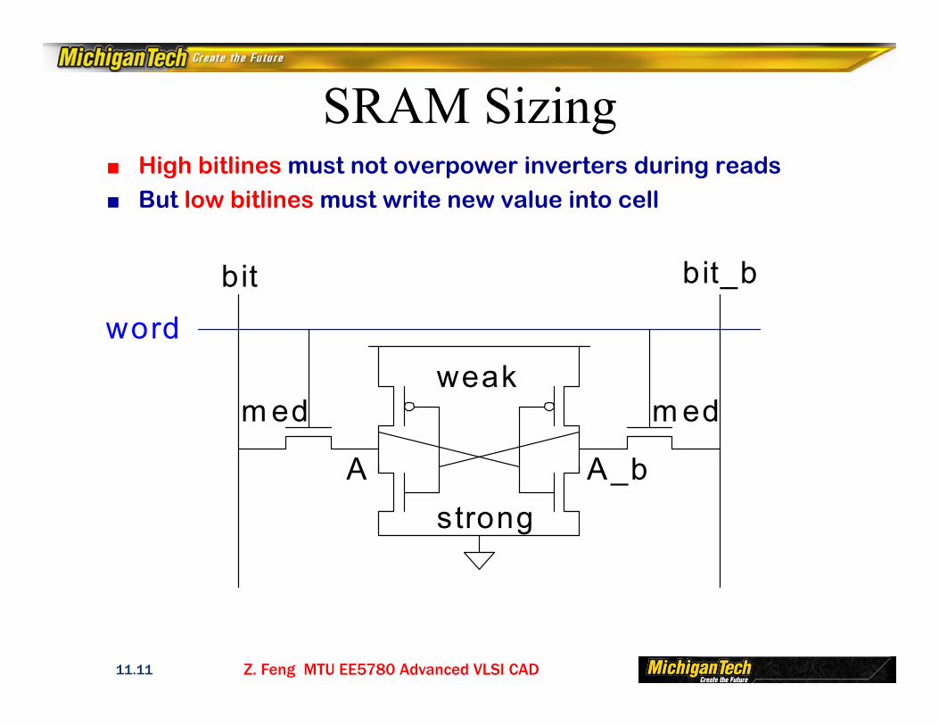
SRAM Sizing■ High bitlines must not overpower inverters during reads■ But low bitlines must write new value into cell
bit bit_b
m ed
A
weak
strong
m ed
A_b
word
Z. Feng MTU EE5780 Advanced VLSI CAD11.12
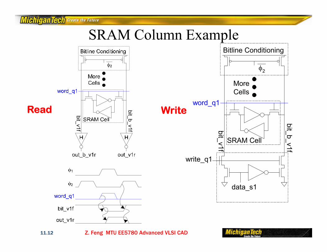
SRAM Column Example
bit_v1f
bit_b_v1f
2
MoreCells
SRAM Cell
word_q1bit_v1f
bit_b_v1f
data_s1
write_q1
Bitline Conditioning
Read Write
Z. Feng MTU EE5780 Advanced VLSI CAD11.13
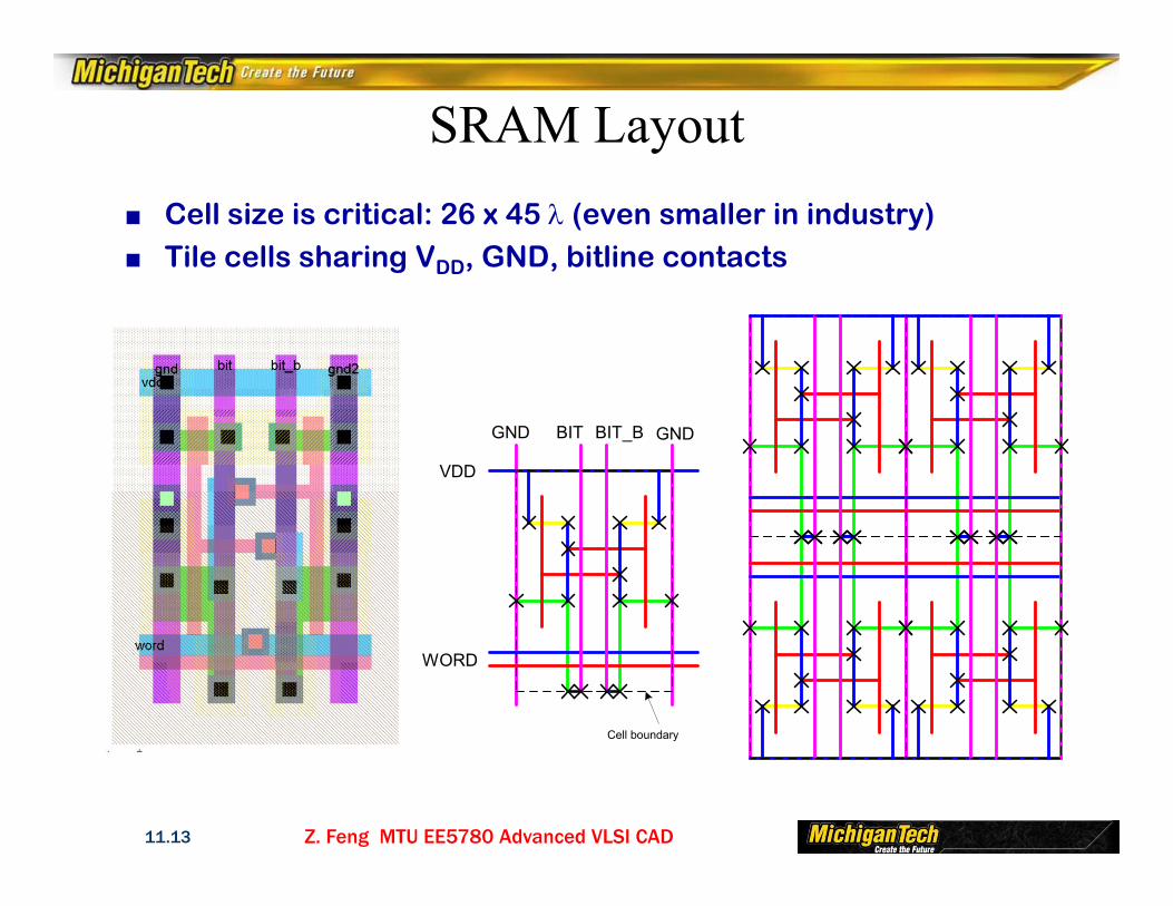
SRAM Layout■ Cell size is critical: 26 x 45 (even smaller in industry)■ Tile cells sharing VDD, GND, bitline contacts
VDD
GND GNDBIT BIT_B
WORD
Cell boundary
Z. Feng MTU EE5780 Advanced VLSI CAD11.14
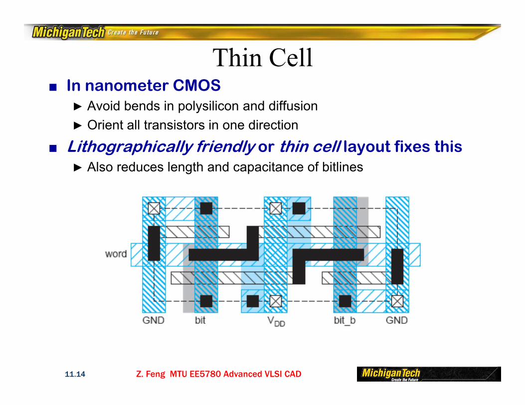
Thin Cell■ In nanometer CMOS
► Avoid bends in polysilicon and diffusion► Orient all transistors in one direction
■ Lithographically friendly or thin cell layout fixes this► Also reduces length and capacitance of bitlines
Z. Feng MTU EE5780 Advanced VLSI CAD11.15
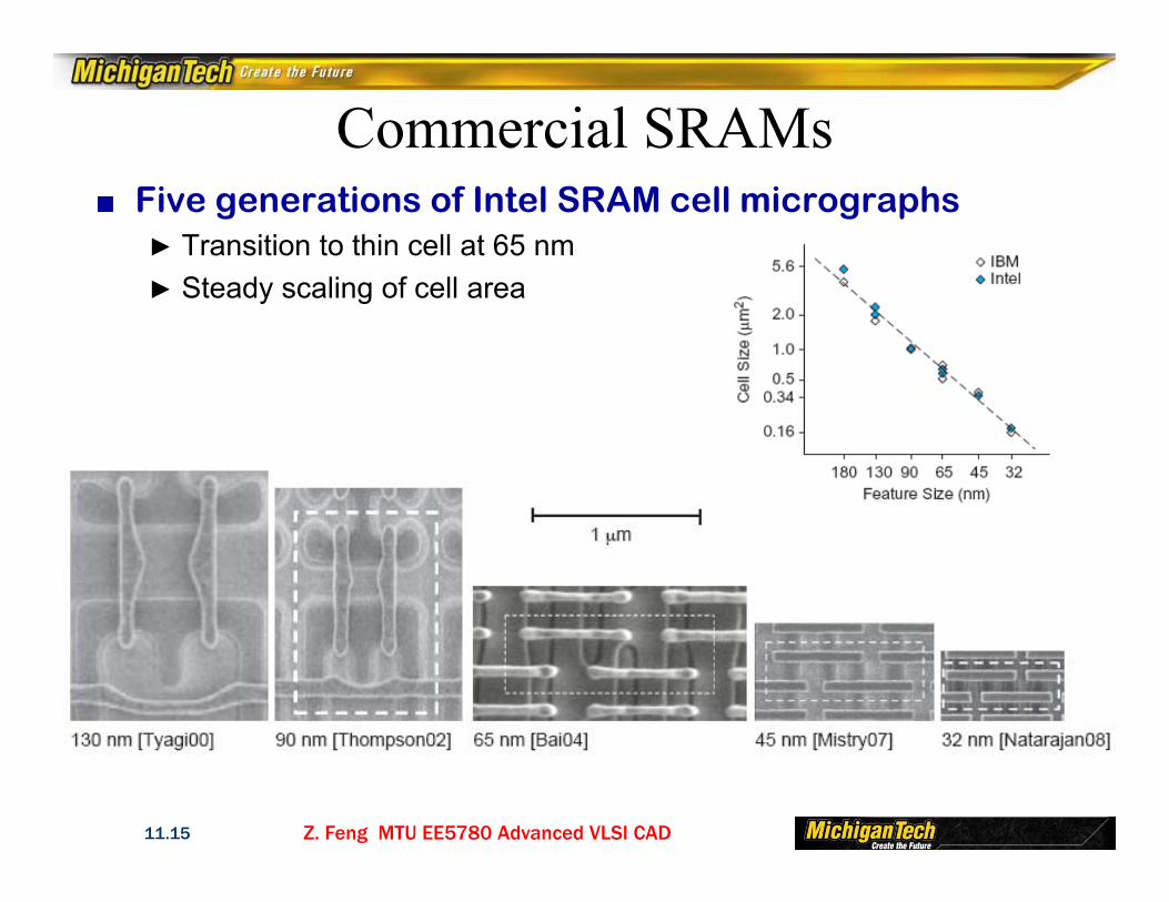
Commercial SRAMs■ Five generations of Intel SRAM cell micrographs
► Transition to thin cell at 65 nm► Steady scaling of cell area
Z. Feng MTU EE5780 Advanced VLSI CAD11.16
Decoders■ n:2n decoder consists of 2n n-input AND gates
► One needed for each row of memory► Build AND from NAND or NOR gates
Static CMOS Pseudo-nMOS
word0
word1
word2
word3
A0A1
A1word
A0 1 1
1/2
2
4
8
16word
A0
A1
11
11
4
8
word0
word1
word2
word3
A0A1
Z. Feng MTU EE5780 Advanced VLSI CAD11.17
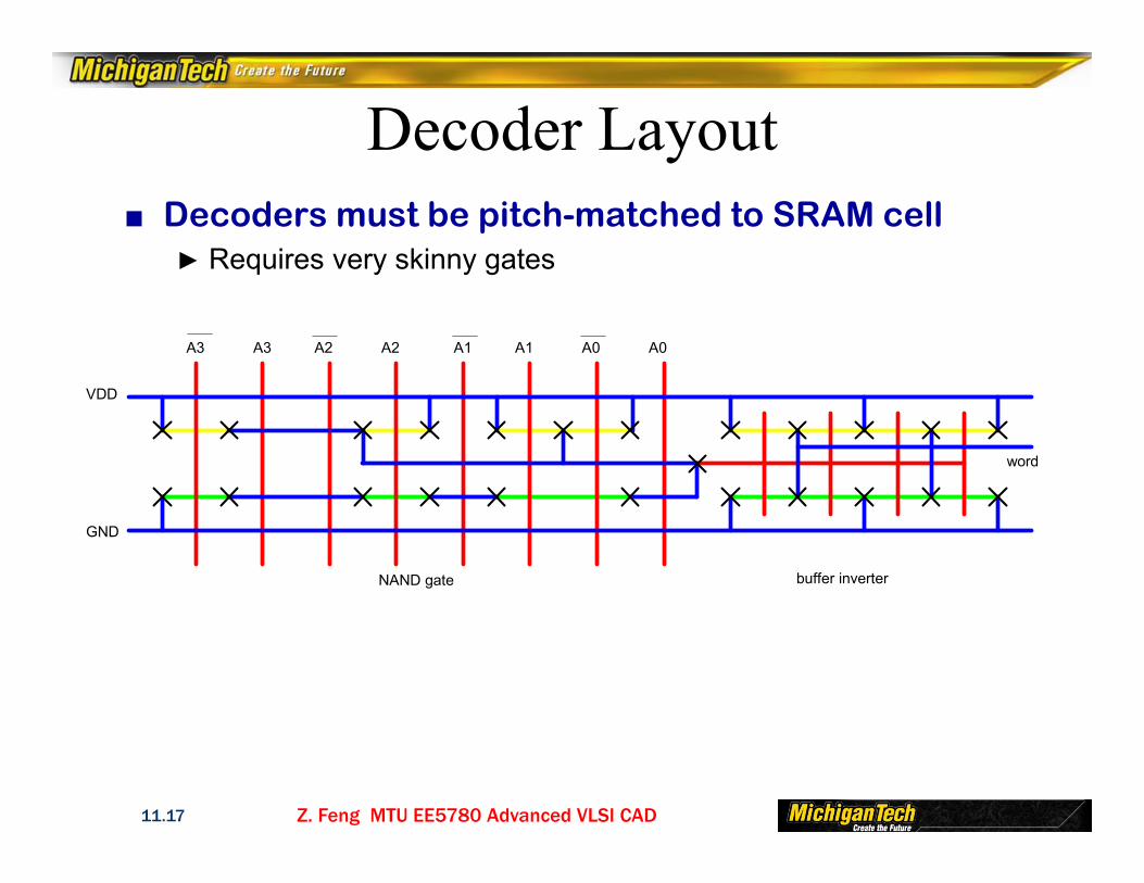
Decoder Layout■ Decoders must be pitch-matched to SRAM cell
► Requires very skinny gates
GND
VDD
word
buffer inverterNAND gate
A0A0A1A2A3 A2A3 A1
Z. Feng MTU EE5780 Advanced VLSI CAD11.18
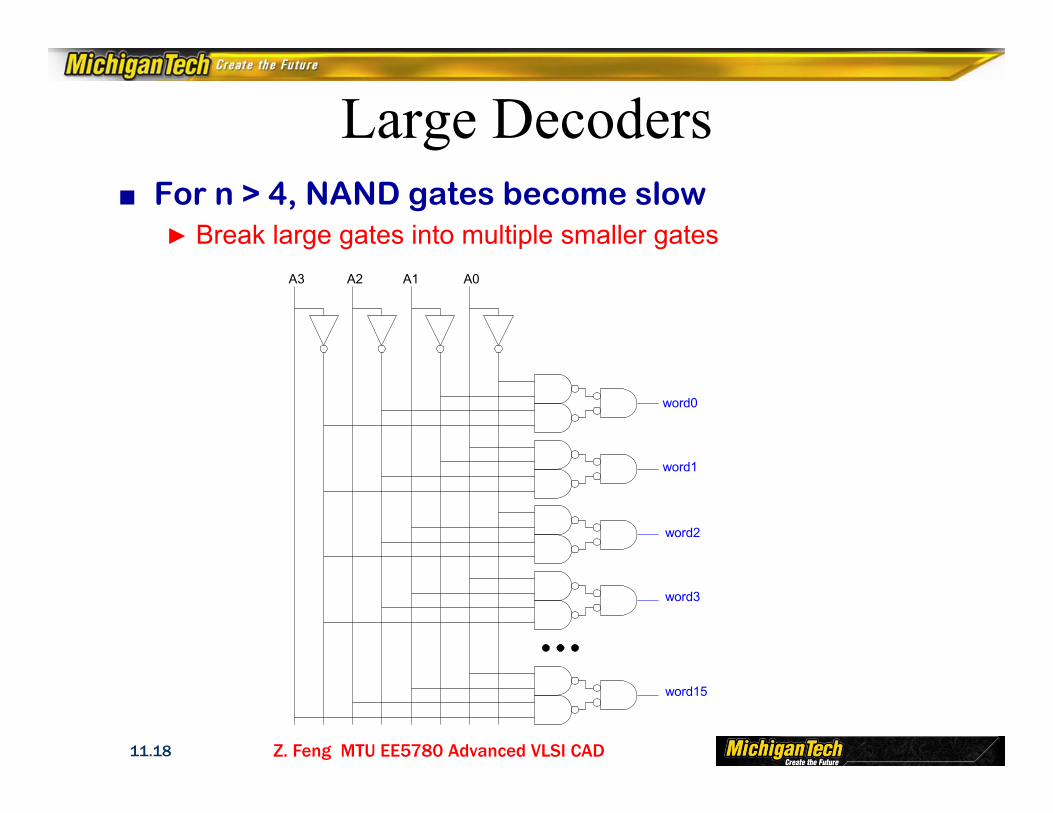
Large Decoders■ For n > 4, NAND gates become slow
► Break large gates into multiple smaller gates
word0
word1
word2
word3
word15
A0A1A2A3
Z. Feng MTU EE5780 Advanced VLSI CAD11.19
Column Circuitry■ Some circuitry is required for each column
► Bitline conditioning► Sense amplifiers► Column multiplexing
Z. Feng MTU EE5780 Advanced VLSI CAD11.20
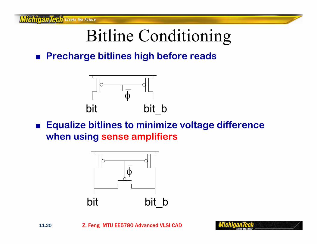
Bitline Conditioning■ Precharge bitlines high before reads
■ Equalize bitlines to minimize voltage difference when using sense amplifiers
bit bit_b
bit bit_b
Z. Feng MTU EE5780 Advanced VLSI CAD11.21
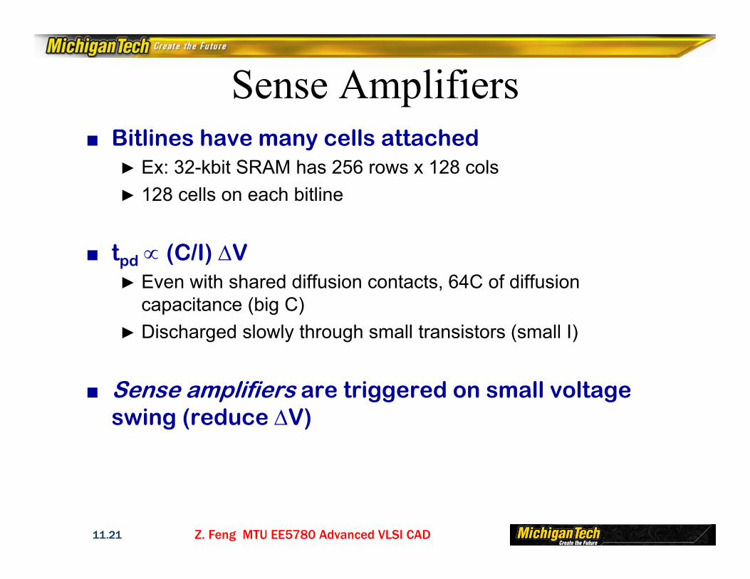
Sense Amplifiers■ Bitlines have many cells attached
► Ex: 32-kbit SRAM has 256 rows x 128 cols► 128 cells on each bitline
■ tpd (C/I) V► Even with shared diffusion contacts, 64C of diffusion
capacitance (big C)► Discharged slowly through small transistors (small I)
■ Sense amplifiers are triggered on small voltage swing (reduce V)
Z. Feng MTU EE5780 Advanced VLSI CAD11.22
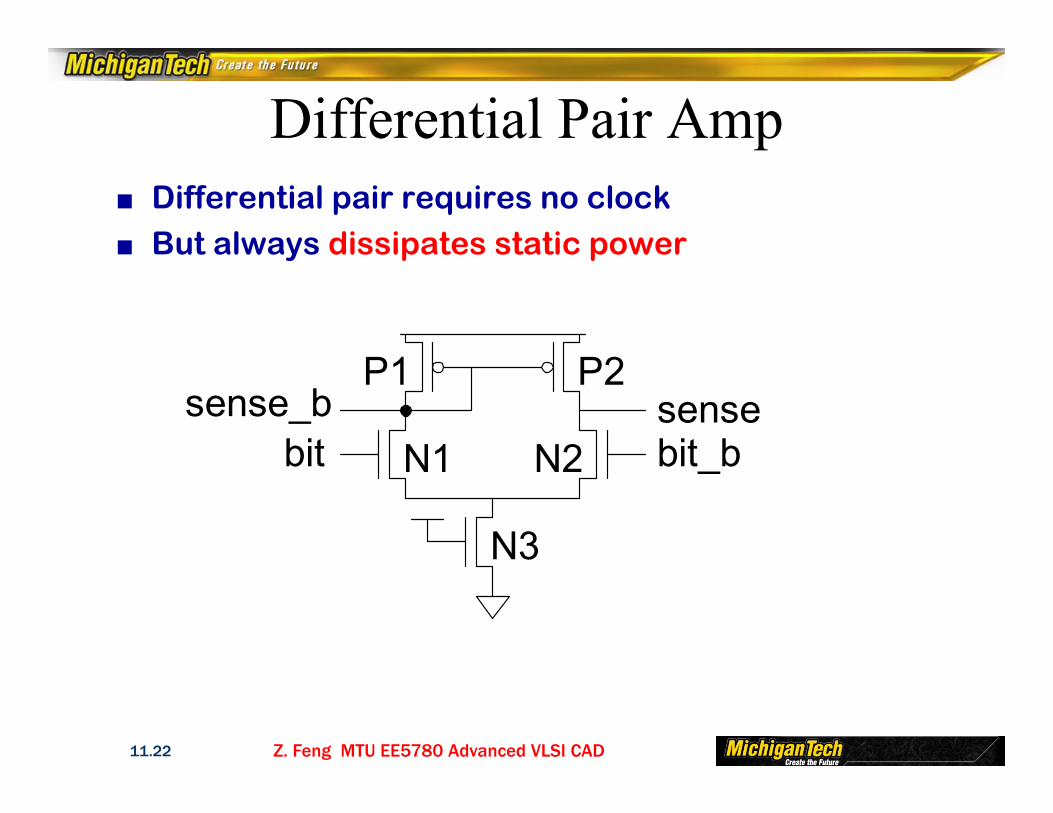
Differential Pair Amp■ Differential pair requires no clock■ But always dissipates static power
bit bit_bsense_b sense
N1 N2
N3
P1 P2

Z. Feng MTU EE5780 Advanced VLSI CAD11.23
Clocked Sense Amp■ Clocked sense amp saves power■ Requires sense_clk after enough bitline swing■ Isolation transistors cut off large bitline
capacitance
bit_bbit
sense sense_b
sense_clk isolationtransistors
regenerativefeedback
Z. Feng MTU EE5780 Advanced VLSI CAD11.24
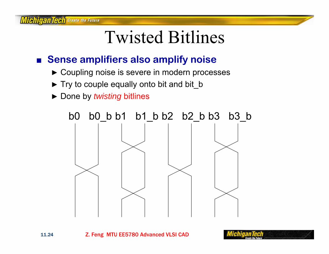
Twisted Bitlines■ Sense amplifiers also amplify noise
► Coupling noise is severe in modern processes► Try to couple equally onto bit and bit_b► Done by twisting bitlines
b0 b0_b b1 b1_b b2 b2_b b3 b3_b
Z. Feng MTU EE5780 Advanced VLSI CAD11.25
Column Multiplexing■ Recall that array may be folded for good aspect ratio
■ Ex: 2k word x 16 folded into 256 rows x 128 columns► Must select 16 output bits from the 128 columns► Requires 16 8:1 column multiplexers
Z. Feng MTU EE5780 Advanced VLSI CAD11.26
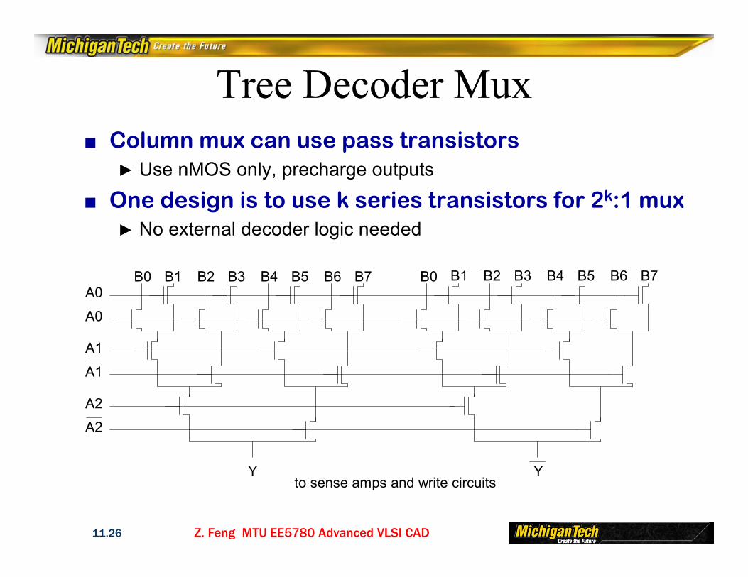
Tree Decoder Mux■ Column mux can use pass transistors
► Use nMOS only, precharge outputs
■ One design is to use k series transistors for 2k:1 mux► No external decoder logic needed
B0 B1 B2 B3 B4 B5 B6 B7 B0 B1 B2 B3 B4 B5 B6 B7A0
A0
A1
A1
A2
A2
Y Yto sense amps and write circuits
Z. Feng MTU EE5780 Advanced VLSI CAD11.27
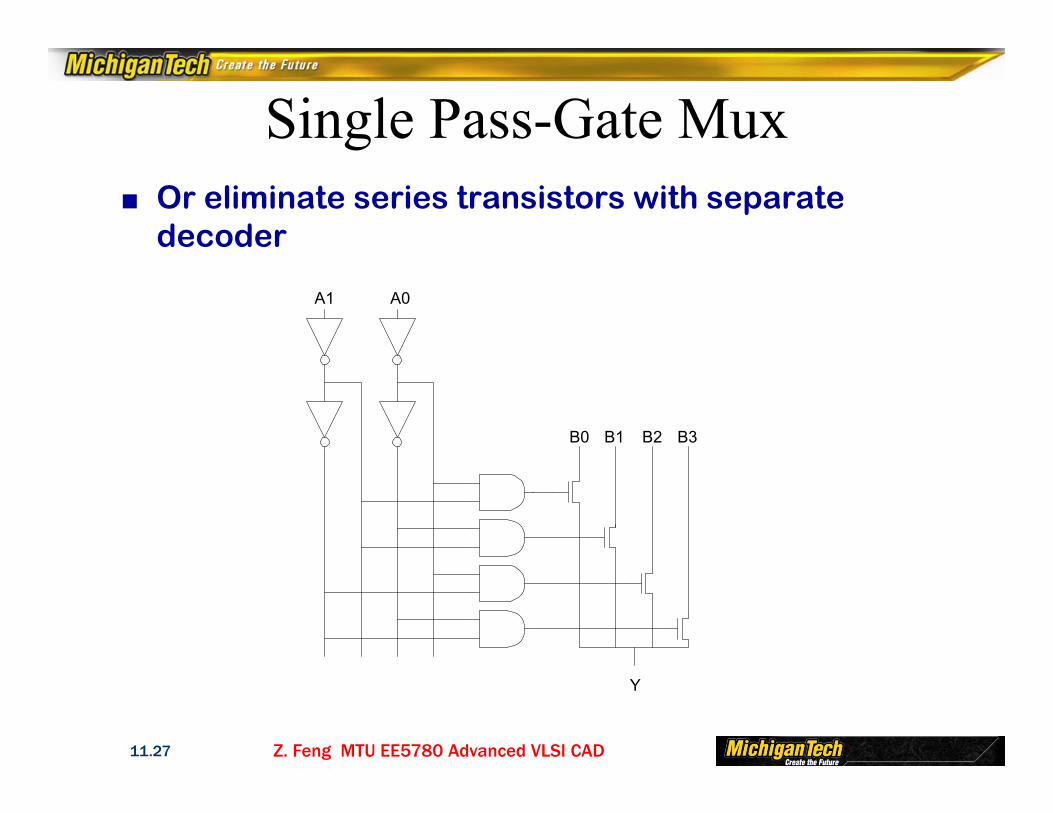
Single Pass-Gate Mux■ Or eliminate series transistors with separate
decoder
A0A1
B0 B1 B2 B3
Y
Z. Feng MTU EE5780 Advanced VLSI CAD11.28
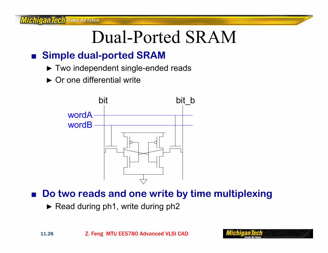
Dual-Ported SRAM■ Simple dual-ported SRAM
► Two independent single-ended reads► Or one differential write
■ Do two reads and one write by time multiplexing► Read during ph1, write during ph2
bit bit_b
wordBwordA

Z. Feng MTU EE5780 Advanced VLSI CAD11.29
Large SRAMs■ Large SRAMs are split into subarrays for speed■ Ex: UltraSparc 512KB cache
► 4 128 KB subarrays► Each have 16 8KB banks► 256 rows x 256 cols / bank► 60% subarray area efficiency► Also space for tags & control
[Shin05]
Z. Feng MTU EE5780 Advanced VLSI CAD11.30
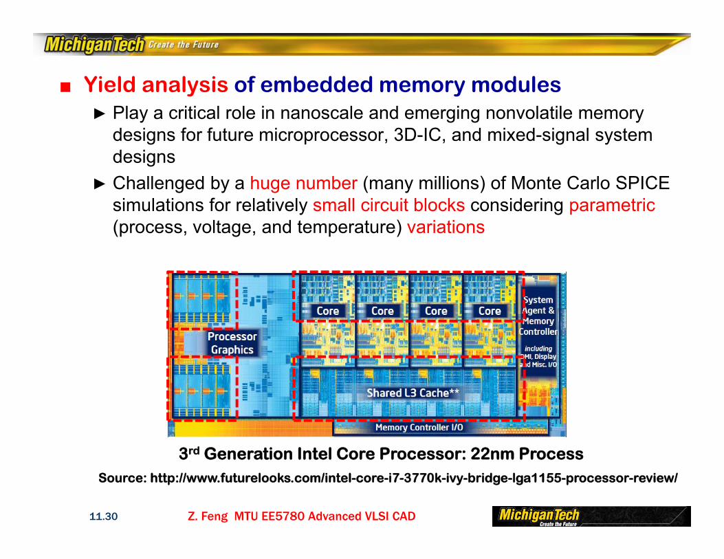
■ Yield analysis of embedded memory modules► Play a critical role in nanoscale and emerging nonvolatile memory
designs for future microprocessor, 3D-IC, and mixed-signal system designs
► Challenged by a huge number (many millions) of Monte Carlo SPICE simulations for relatively small circuit blocks considering parametric(process, voltage, and temperature) variations
3rd Generation Intel Core Processor: 22nm ProcessSource: http://www.futurelooks.com/intel-core-i7-3770k-ivy-bridge-lga1155-processor-review/
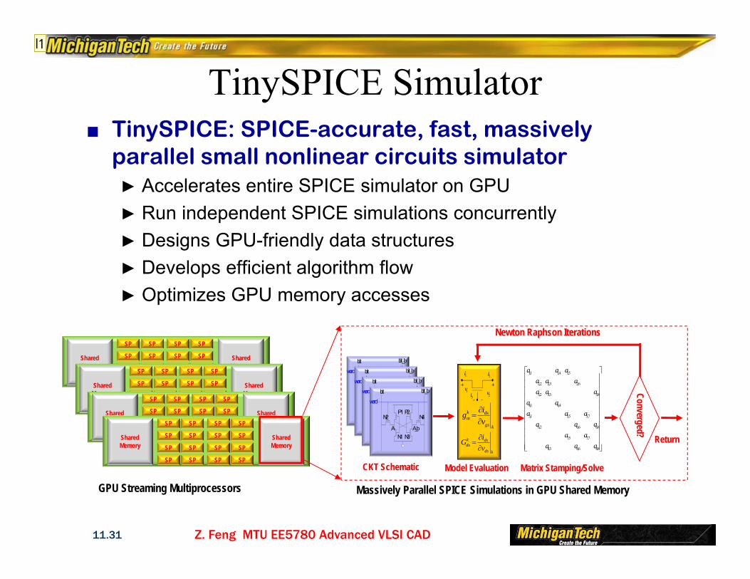
Z. Feng MTU EE5780 Advanced VLSI CAD11.31
TinySPICE Simulator■ TinySPICE: SPICE-accurate, fast, massively
parallel small nonlinear circuits simulator► Accelerates entire SPICE simulator on GPU► Run independent SPICE simulations concurrently► Designs GPU-friendly data structures► Develops efficient algorithm flow► Optimizes GPU memory accesses
SP SP
SP SP
SP SP
SP SP
SP SP
SP SP
SP SP
SP SP
Shared Memory
Shared Memory
bit bit_b
N1
N2P1
A
P2
N3
N4
A_b
word bit bit_b
N1
N2P1
A
P2
N3
N4
A_b
word
bit bit_b
N1
N2P1
A
P2
N3
N4
A_b
word bit bit_b
N1
N2P1
A
P2
N3
N4
A_b
word bit bit_b
N1
N2P1
A
P2
N3
N4
A_b
word
1i 2i
2v1v
3i
kgs
dskm v
ig
kds
dskds v
iG
1,1 1,4 1,5
2,2 2,3 2,6
3,2 3,3 3,8
4,1 4,4
5,1 5,5 5,7
6,2 6,6 6,8
7,5 7,7
8,3 8,6 8,8
a a aa a aa a a
a aa a a
a a aa a
a a a
SP SP
SP SP
SP SP
SP SP
SP SP
SP SP
SP SP
SP SP
Shared Memory
Shared Memory
SP SP
SP SP
SP SP
SP SP
SP SP
SP SP
SP SP
SP SP
Shared Memory
Shared Memory SP SP
SP SP
SP SP
SP SP
SP SP
SP SP
SP SP
SP SP
Shared Memory
Shared Memory
CKT Schematic Model Evaluation Matrix Stamping/Solve
Converged?
Return
Newton Raphson Iterations
GPU Streaming Multiprocessors Massively Parallel SPICE Simulations in GPU Shared Memory
l1
Slide 31
l1 lengfei, 5/13/2013
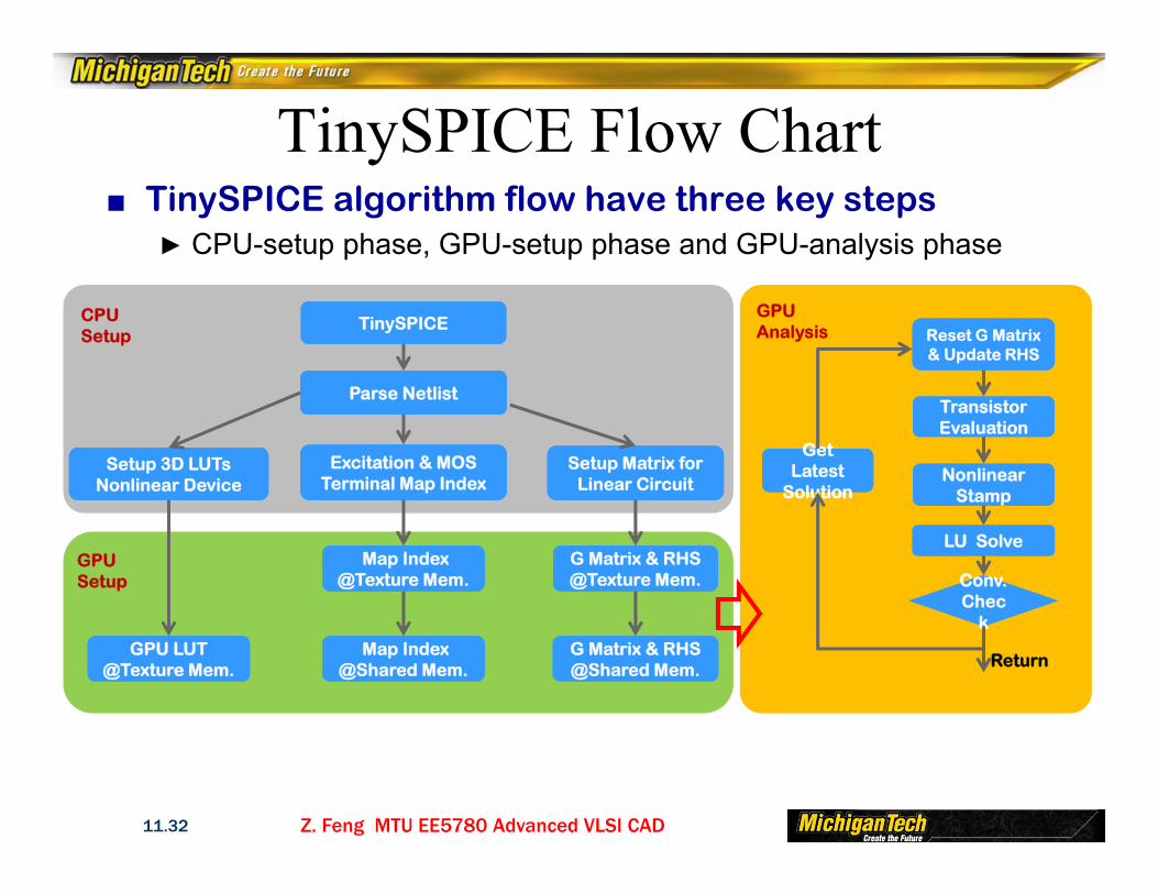
Z. Feng MTU EE5780 Advanced VLSI CAD11.32
TinySPICE Flow Chart
TinySPICETinySPICE
Parse NetlistParse Netlist
Setup 3D LUTsNonlinear Device
Setup 3D LUTsNonlinear Device
Excitation & MOS Terminal Map Index
Excitation & MOS Terminal Map Index
Setup Matrix forLinear Circuit
Setup Matrix forLinear Circuit
G Matrix & RHS@Shared Mem.G Matrix & RHS@Shared Mem.
CPU Setup
GPU Setup
G Matrix & RHS@Texture Mem.G Matrix & RHS@Texture Mem.
Map Index@Texture Mem.
Map Index@Texture Mem.
GPU Analysis
Get Latest
Solution
Get Latest
Solution
Reset G Matrix& Update RHSReset G Matrix& Update RHS
Transistor EvaluationTransistor Evaluation
Nonlinear Stamp
Nonlinear Stamp
LU SolveLU Solve
Conv. Chec
k
Conv. Chec
k
ReturnMap Index
@Shared Mem.Map Index
@Shared Mem.GPU LUT
@Texture Mem.GPU LUT
@Texture Mem.
■ TinySPICE algorithm flow have three key steps► CPU-setup phase, GPU-setup phase and GPU-analysis phase
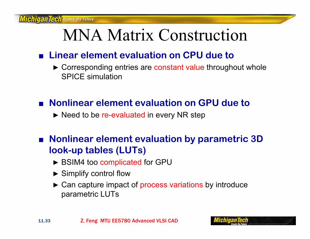
Z. Feng MTU EE5780 Advanced VLSI CAD11.33
MNA Matrix Construction■ Linear element evaluation on CPU due to
► Corresponding entries are constant value throughout whole SPICE simulation
■ Nonlinear element evaluation on GPU due to► Need to be re-evaluated in every NR step
■ Nonlinear element evaluation by parametric 3D look-up tables (LUTs)► BSIM4 too complicated for GPU► Simplify control flow► Can capture impact of process variations by introduce
parametric LUTs
Z. Feng MTU EE5780 Advanced VLSI CAD11.34
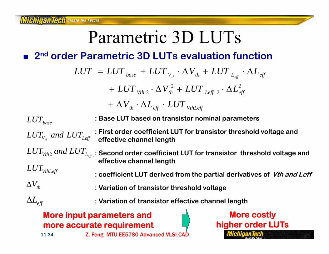
Parametric 3D LUTs
VthLeffeffth
effLeffthVth
effLthVbase
LUTLV
LLUTVLUT
LLUTVLUTLUTLUTeffth
2
22
2
baseLUT
LeffV LUTandLUTth
22 effLVth LUTandLUT
thV
effL
: Base LUT based on transistor nominal parameters
: First order coefficient LUT for transistor threshold voltage andeffective channel length
: Second order coefficient LUT for transistor threshold voltage and effective channel length
: Variation of transistor threshold voltage
: Variation of transistor effective channel length
VthLeffLUT: coefficient LUT derived from the partial derivatives of Vth and Leff
■ 2nd order Parametric 3D LUTs evaluation function
More input parameters andmore accurate requirement
More costly higher order LUTs
Z. Feng MTU EE5780 Advanced VLSI CAD11.35
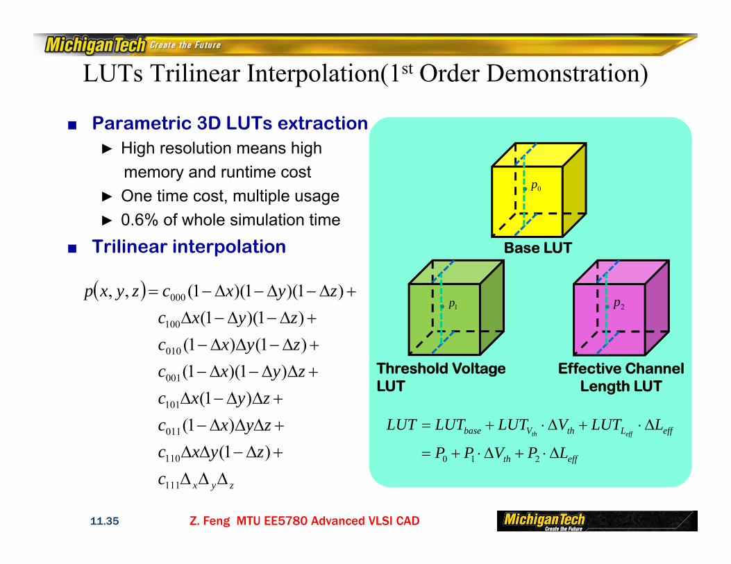
■ Parametric 3D LUTs extraction► High resolution means high
memory and runtime cost► One time cost, multiple usage► 0.6% of whole simulation time
■ Trilinear interpolation
LUTs Trilinear Interpolation(1st Order Demonstration)
zyxczyxczyxczyxc
zyxczyxczyxc
zyxczyxp
111
110
011
101
001
010
100
000
)1()1(
)1()1)(1(
)1()1()1)(1(
)1)(1)(1(,,
effth
effLthVbase
LPVPP
LLUTVLUTLUTLUTeffth
210
0p
Base LUT
1p
Threshold Voltage LUT
2p
Effective Channel Length LUT
Z. Feng MTU EE5780 Advanced VLSI CAD11.36
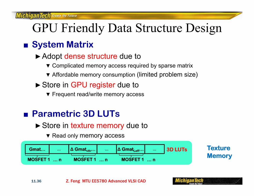
GPU Friendly Data Structure Design■ System Matrix
►Adopt dense structure due to▼Complicated memory access required by sparse matrix▼Affordable memory consumption (limited problem size)
►Store in GPU register due to▼Frequent read/write memory access
■ Parametric 3D LUTs►Store in texture memory due to
▼Read only memory access
Gmat… 3D LUTs
MOSFET 1 … n
∆ Gmatvth… ∆ GmatLeff…… … …
MOSFET 1 … n MOSFET 1 … n
TextureMemory
Z. Feng MTU EE5780 Advanced VLSI CAD11.37
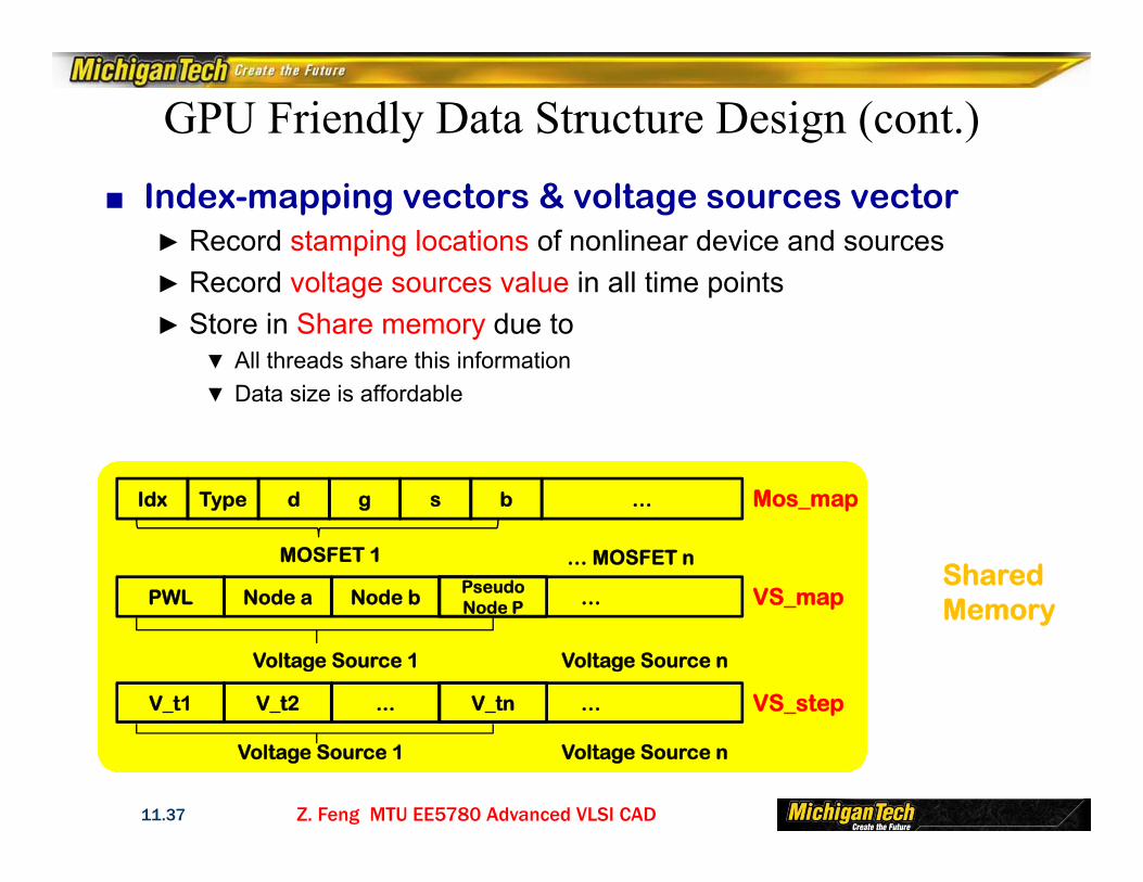
GPU Friendly Data Structure Design (cont.)■ Index-mapping vectors & voltage sources vector
► Record stamping locations of nonlinear device and sources► Record voltage sources value in all time points► Store in Share memory due to
▼ All threads share this information▼ Data size is affordable
V_t1 V_t2 … VS_step
Voltage Source 1 Voltage Source n
... V_tn
PWL Node a … VS_map
Voltage Source 1
Idx Type d g s b … Mos_map
MOSFET 1 … MOSFET n
Voltage Source n
Node b PseudoNode P
SharedMemory
Z. Feng MTU EE5780 Advanced VLSI CAD11.38
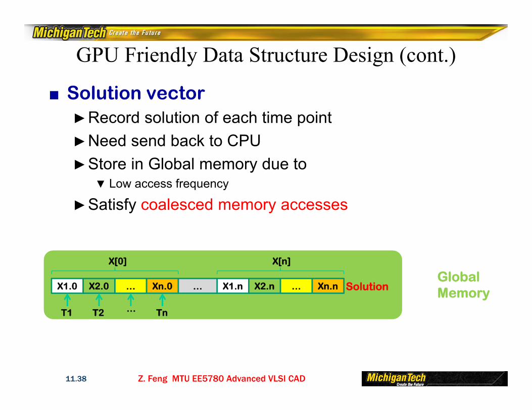
GPU Friendly Data Structure Design (cont.)
■ Solution vector►Record solution of each time point►Need send back to CPU ►Store in Global memory due to
▼Low access frequency
►Satisfy coalesced memory accesses
X1.0 X2.0 … Xn.0 X1.n X2.n … Xn.n…
T1 T2 Tn
X[0] X[n]
…
SolutionGlobalMemory

Z. Feng MTU EE5780 Advanced VLSI CAD11.39
Newton-Raphson Algorithm on GPU■ Check convergence after several NR iterations
► Reduces the GPU thread divergence► Leads some overhead
Get Latest Solution
Get Latest Solution
Reset G Matrix& Update RHSReset G Matrix& Update RHS
Transistor EvaluationTransistor Evaluation
Nonlinear StampNonlinear Stamp
LU SolveLU Solve
Return
Conv. CheckConv. Check
Get Latest Solution
Get Latest Solution
Reset G Matrix& Update RHSReset G Matrix& Update RHS
Transistor EvaluationTransistor Evaluation
Nonlinear StampNonlinear Stamp
LU SolveLU Solve
Conv. CheckConv. Check
Return
Time to CheckTime to Check
Z. Feng MTU EE5780 Advanced VLSI CAD11.40
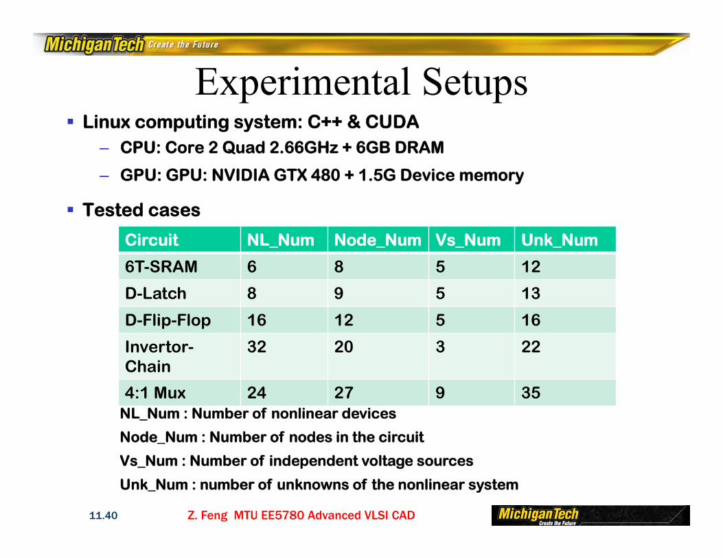
Linux computing system: C++ & CUDA– CPU: Core 2 Quad 2.66GHz + 6GB DRAM
– GPU: GPU: NVIDIA GTX 480 + 1.5G Device memory
Tested cases
Experimental Setups
Circuit NL_Num Node_Num Vs_Num Unk_Num
6T-SRAM 6 8 5 12
D-Latch 8 9 5 13
D-Flip-Flop 16 12 5 16
Invertor-Chain
32 20 3 22
4:1 Mux 24 27 9 35NL_Num : Number of nonlinear devices
Node_Num : Number of nodes in the circuit
Vs_Num : Number of independent voltage sources
Unk_Num : number of unknowns of the nonlinear system
Z. Feng MTU EE5780 Advanced VLSI CAD11.41
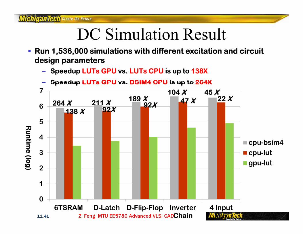
Run 1,536,000 simulations with different excitation and circuit design parameters
– Speedup LUTs GPU vs. LUTs CPU is up to 138X
– Speedup LUTs GPU vs. BSIM4 CPU is up to 264X
DC Simulation Result
Ru
ntim
e(lo
g)
264 X138 X
211 X92X
189 X92X
104 X47 X 22 X
45 X
Z. Feng MTU EE5780 Advanced VLSI CAD11.42
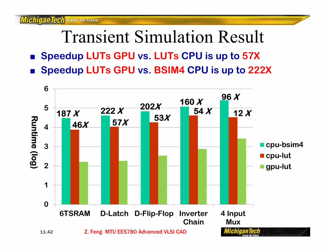
Transient Simulation Result■ Speedup LUTs GPU vs. LUTs CPU is up to 57X■ Speedup LUTs GPU vs. BSIM4 CPU is up to 222X
Ru
ntim
e(lo
g)
187 X46X
222 X57X
202X53X
160 X54 X 12 X
96 X
Z. Feng MTU EE5780 Advanced VLSI CAD11.43
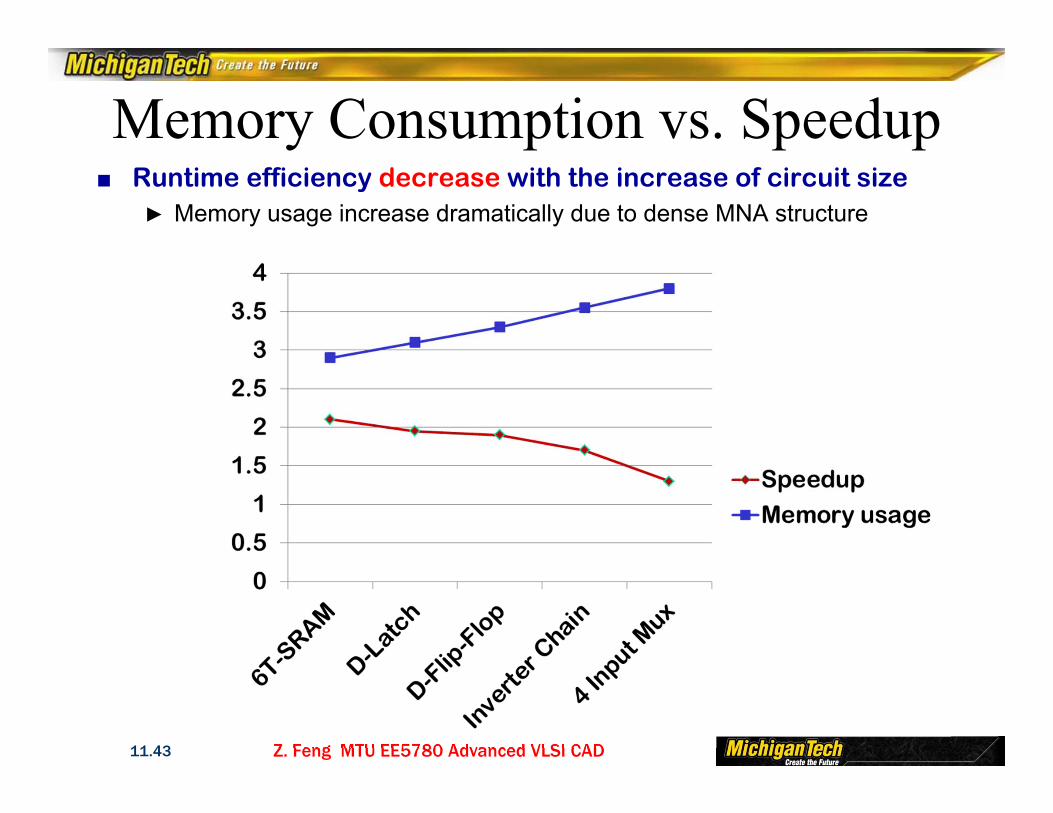
Memory Consumption vs. Speedup■ Runtime efficiency decrease with the increase of circuit size
► Memory usage increase dramatically due to dense MNA structure


![Parallel VLSI CAD Algorithmszhuofeng/EE5900Spring2012... · Parallel VLSI CAD Algorithms Lecture 1 Introduction ... Various IEEE journal and conference papers: IEEE[1] Various IEEE](https://img.dokumen.tips/doc/110x75/5e88f1299475ec1f5a74fb96/parallel-vlsi-cad-algorithms-zhuofengee5900spring2012-parallel-vlsi-cad-algorithms.jpg)