Embed Size (px)
Citation preview

2/8/11
1
1 tanford University araswat
EE410
EE410 Test Structures & Testing
Krishna Saraswat Department of Electrical Engineering
Stanford University
2 tanford University araswat
EE410
What's on the New EE410 CMOS Chip?
The CMOS-LOCOS wafer contains 80 dice, each die measuring 8.3mm x 8.3mm. 1. Fabrication Test Structures —
checked during processing 2. Device Test Structures —
MOSFET's, parasitic MOS & BJTs, capacitors, diodes
3. Process Test Structures — sheet resistance, contacts, continuity, isolation
4. Circuit Test Structures — CMOS inverters
5. Research Test Structures (Not used in EE410)

2/8/11
2
3 tanford University araswat
EE410
EE 410 Chip
4 tanford University araswat
EE410
EE410 Mask Layout

2/8/11
3
5 tanford University araswat
EE410
What you need to do for EE410?
• Confirm that process works. If it doesn't, find out why. • Test every unique structure at least once, but don't waste time testing
everything. • Gather some statistics only on important parameters such as threshold
voltages and diode leakage currents. Examine across-wafer and wafer-to-wafer variations. But once again, don't measure everything.
• Identify a processing mistake which was ”intentionally" introduced. (only one mistake on each "bad" wafer)
• Make comparisons with simulated and hand-calculated results wherever possible.
• Compare results obtained from different measurement techniques. e.g • oxide thickness — Nanospec vs. CV • threshold voltage — ID-VGS vs. CV
6 tanford University araswat
EE410
WAFER PROBING • Access device terminals by probing 100µm × 160µm
metal pads situated on thick oxide (field region). • Pads are arranged in 10 × 2 arrays to accommodate
automated probe tester (not used in EE410). • There are no shared connections between adjacent
structures. • Once all probe tips are positioned, only the probe
station stage needs to be raised or lowered to move to the next device.
• The wafer backside is not used as a contact. • Example D-1 and D-2
– L (Length) SERIES (W=100µm) – L ranging from 100 to 1µm in D-1 and 0.75 to 0.45 µm in D-2
• This set of pads allows you to access 5 different NMOS transistors of fixed gate width and variable gate lengths in each series.
Refer to EE410 CMOS LOCOS Manual Appendix A — List of Test Structures Appendix B — Pad Assignments
Pad Assignments NMOS Length Series Pad Assignments
N M OS L E N G T H SE RI ES
D-1 W/L = 100um / 100um
W/L = 100um / 25um
W/L = 100um / 5um
W/L = 100um / 2.5um
W/L = 100um / 1um
D-2 W/L = 100um / 0.75um
W/L = 100um / 0.6um
W/L = 100um / 0.55um
W/L = 100um / 0.5um
W/L = 100um / 0.45um
GATE DRAIN
P-WELL SOURCE
GATE DRAIN
P-WELL SOURCE
GATE DRAIN
P-WELL SOURCE
GATE DRAIN
P-WELL SOURCE
GATE DRAIN
P-WELL SOURCE
GATE DRAIN
P-WELL SOURCE
GATE DRAIN
P-WELL SOURCE
GATE DRAIN
P-WELL SOURCE
GATE DRAIN
P-WELL SOURCE
GATE DRAIN
P-WELL SOURCE

2/8/11
4
7 tanford University araswat
EE410
DEVICE TEST STRUCTURES
• p-n diodes • MOS capacitors • MOSFETs • Parasitic BJTs
8 tanford University araswat
EE410
Diodes
• Extract both area and edge components of diode current. • Need to measure low current levels — watch out for noise
sources. • Can reduce surface leakage by applying nitrogen stream to
remove surface moisture. • Examine characteristics of poly-poly diode. • Measure breakdown and CV characteristics. • Are diode leakages acceptable?
!
IDiode = I0 " eqV/nkT #1( )

2/8/11
5
9 tanford University araswat
EE410
Capacitors p-polyn-poly
LTO-PSGAl/Si alloy
field oxidegate oxide
n-substrate
p-well
Capacitance-Voltage Measurements • High-frequency CV (accumulation, depletion, inversion, deep depletion)
• Low-frequency (quasi-static) CV Not to be done
• Combined high-how frequency CV — measure interface trap density
Not to be done
!
qDit =1
1CLF" 1
COX
"1
1CHF
" 1COX
10 tanford University araswat
EE410
GATE
SOURCE
DRAIN
P-WELLW/L
!
ID =µNCOX2
Weff
Leff2 VGS " VT( ) " VDS[ ]VDS
!
IDSAT =µ NCOX2
Weff
LeffVGS " VT( )2 1+ #VDS( )
Triode Region
Saturation Region
GATE
SOURCE
DRAIN
N-SUBSTRATEW/L
NMOS & PMOS Transistors
2/8/11
6
11 tanford University araswat
EE410
Parasitic Transistors: MOSFETs
• Isolation — are parasitic channel thresholds sufficiently large (i.e., |VT| » VDD)?
• Two types: polysilicon on field oxide, metal on BPSG + field oxide
• Good agreement with SUPREM-III predictions?
n-substrate p-well
metal poly
parasiticPMOS parasitic
NMOS
12 tanford University araswat
EE410
Parasitic Transistors: BJT's
n+ n+p+
p-welln-substrate
Emitter Poly Mask Base Collector
BaseWidth
(a)
polyoxide
metal
Latchup — are parasitic β's sufficiently low?
n+ p+p+
p-welln-substrate
EmitterPoly MaskBase CollectorPoly Mask
BaseWidth
(c)
poly polyoxide
metal
2/8/11
7
13 tanford University araswat
EE410
PROCESS TEST STRUCTURES
Purpose – Extract very specific electrical information about the process. – Identify process problems. – Improve process.
• Sheet resistance • Contact Chain • Contact Resistance • Continuity and Isolation
14 tanford University araswat
EE410
Sheet Resistance
• Force a current and measure the resulting voltage. • 4-point probe vs. van der Pauw • Compare measured results with simulated and hand-calculated
values.
I-1 FORCE I-2 FORCE
V-1 SENSE V-2 SENSE
L
W
VDP-1
VDP-2 VDP-3
VDP-4
Metal Contact Hole
Specified Wafer Layer
4-Point Probe Structure Van der Pauw Structure
2/8/11
8
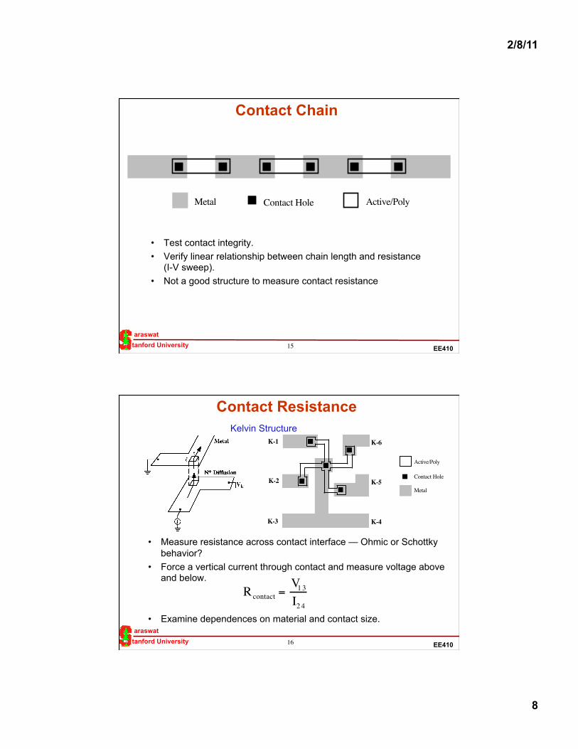
15 tanford University araswat
EE410
Contact Chain
• Test contact integrity. • Verify linear relationship between chain length and resistance
(I-V sweep). • Not a good structure to measure contact resistance
Contact Hole Active/PolyMetal
16 tanford University araswat
EE410
Contact Resistance
• Measure resistance across contact interface — Ohmic or Schottky behavior?
• Force a vertical current through contact and measure voltage above and below.
• Examine dependences on material and contact size.
K-1
K-2
K-3 K-4
K-5
K-6
Active/Poly
Contact Hole
Metal
!
Rcontact =V13I24
Kelvin Structure

2/8/11
9
17 tanford University araswat
EE410
Continuity and Isolation • Complementary tests to detect unwanted open and short circuits. • Common sources of failure:
– incomplete etch → stringers – overetch – material failure (breakage) over aggressive topography
A
B
A
B
Large RAB → PASS Continuity Structure Isolation Structure Small RAB → PASS
18 tanford University araswat
EE410
Policies and procedures for EE410 testing"
After the fabrication is complete your TA will give you a demonstration on the testing set up. This will be done during your regular lab time slot. The responsibility of the TA is to get you started. Subsequently he/she wonʼt be present when you are testing.#
Every user should read testing handouts before TA's demonstration and exercise caution when operating the testers. Generally, the probe tips and probe position adjustment screws are the most fragile parts.#
#

2/8/11
10
19 tanford University araswat
EE410
EE 410 - PROBE SIGN-IP SHEETWeek Beginning ……../……../……..
Please Include Name, Group Name, E-mail address and/or phone number in reservation
Sunday Monday Tuesday Wednesday Thursday Friday Saturday
12:00:00 AM
4:00:00 AM
4:00:00 AM
8:00:00 AM
8:00:00 AM
12:00:00 PM
12:00:00 PM
4:00:00 PM
4:00:00 PM
8:00:00 PM
8:00:00 PM
12:00:00 AM
Peak Time I
Peak Time II
Off Peak Time
This sign up sheet will be posted near the testing set up. You also need to reserve the test setup on Coral. Your TA will show you how to do it.
20 tanford University araswat
EE410
Policies and procedures for EE410 testing"A sign up sheet will be posted near the testing set up. You also need to reserve the test setup on Coral. Your TA will show you how to do it. The rules for the testing phase are:
• The time slots for testing have been divided into 4 hours/slot and are classified as
• Peak Time I (8am to 4 pm, Sunday to Saturday), • Peak time II (4 pm to 12am, Sunday to Saturday) and • Off Peak hours (12am to 8 am, Sunday to Saturday).
• Each group is limited to a maximum of 3 reserved slots during Prime Time I inclusive of their regular processing hours, 3 reserved slots during Prime Time II and 3 reserved slots during Off Peak Time.
• Each group is limited to a maximum reservation of 9 time slots per week.

2/8/11
11
21 tanford University araswat
EE410
Policies and procedures for EE410 testing"• The 6 remaining slots are to be left unreserved for other lab
users. • A slot can be taken if no one shows up 15 minutes after the
sign-up time. • You are not allowed to sign-up for 2 consecutive sessions. • No TA support will be provided during nights and weekends. • A minimum of 2 students should always be present for safety
reasons. • Any damage to the test bench must be promptly reported to
Prof. Saraswat or the TAs. Remember, we won’t punish you for breaking the setup but will definitely mind if the incident is hidden from us. Please check the test setup before starting your measurements.
• Write any comment if you think it would benefit others or help avoid damage on the testers.
22 tanford University araswat
EE410
PRACTICAL TESTING & TROUBLESHOOTING
Important tips... • Understand why a test structure is on the chip.
– This tells you what information you can get from the structure and what you need to measure.
• Be able to sketch a cross-section of the test structure to be tested. Some general notes...
• Take good care of the testing setup — it's your only one and it cannot be replaced.
• Be very careful with the probe tips & manipulators — they are very expensive.
• Avoid working alone — it's safer and less frustrating. • BE SAFE — watch out for high currents & voltages (set equipment
compliances). • BE PATIENT & DON'T RUSH — testing is very time-consuming. • Make sure you distribute the chores evenly within your group.

2/8/11
12
23 tanford University araswat
EE410
• Remember: Murphy is always watching you! It's almost always the simplest things that go wrong, so check them first!
• Check the same structure elsewhere first. Never assume anything. Your DUT (device under test) could be defective. You have 6 wafers and 43 dice per wafer, so don't be afraid to look around.
• If you get the same result (no variation), verify your setup. • Some common problems:
wrong connections (e.g., gate and source connections reversed) bad connections (e.g., dirty contact surfaces) faulty cables (a multimeter could be your best friend here) bad probe tips (e.g., high leakage > 10 pA when disconnected) noise — important for low noise, low current measurements
Noise sources are often very difficult to find. Sources may be as obvious (?) as transformer noise coming from the microscope light power supply or may come from fundamental grounding and shielding problems with your probe station.
• If your setup is fine, perform important sanity checks. e.g., for MOSFET's, make sure IGATE = 0 and ISOURCE = IDRAIN
These simple tests may sound silly and unnecessary, but they are the only systematic way to locate your problem.
• You have an exhaustive list of process test structures to your avail. Exploit this luxury to deduce the culprit.
When things don't work...
24 tanford University araswat
EE410
SOME FINAL REMARKS There should be no mystery about testing. If you are unsure, ASK!!!" To make sure you understand the process well, you should be able to:"
• Correlate observed device anomalies with problems in the process test structures."
• Explain differences between prediction and actual measurement."• Explain the consequences of any changes made to the wafers
during processing." To make sure that you have grasped the big picture, you should:"
• Compare measured values with a comparable CMOS process."• Relate compromises in device performance with process
simplicity."• Try to offer improvements to process flow without greatly
increasing complexity."
Good luck and have fun!!