Embed Size (px)
Citation preview
Sam PalermoAnalog & Mixed-Signal Center
Texas A&M University
ECEN325: ElectronicsSpring 2017
A Graphical Approach to BJT Amplifier Design
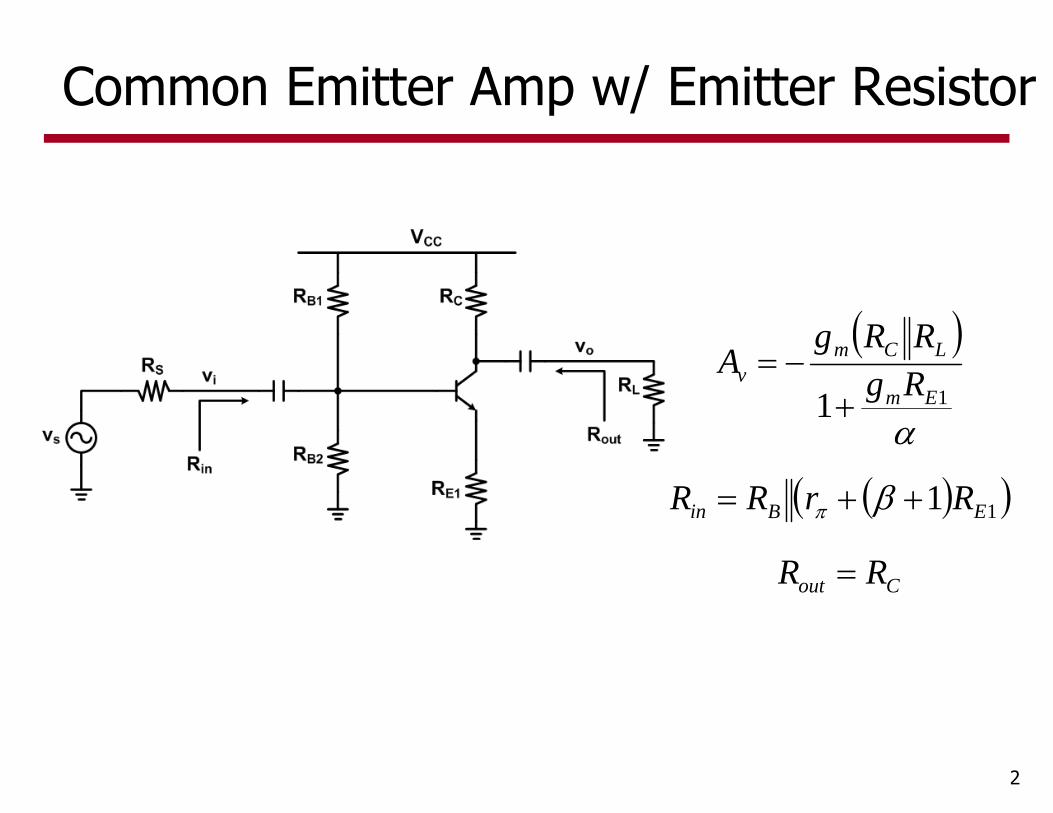
Common Emitter Amp w/ Emitter Resistor
2
Cout
EBin
Em
LCmv
RR
RrRR
RgRRg
A
1
1
1
1
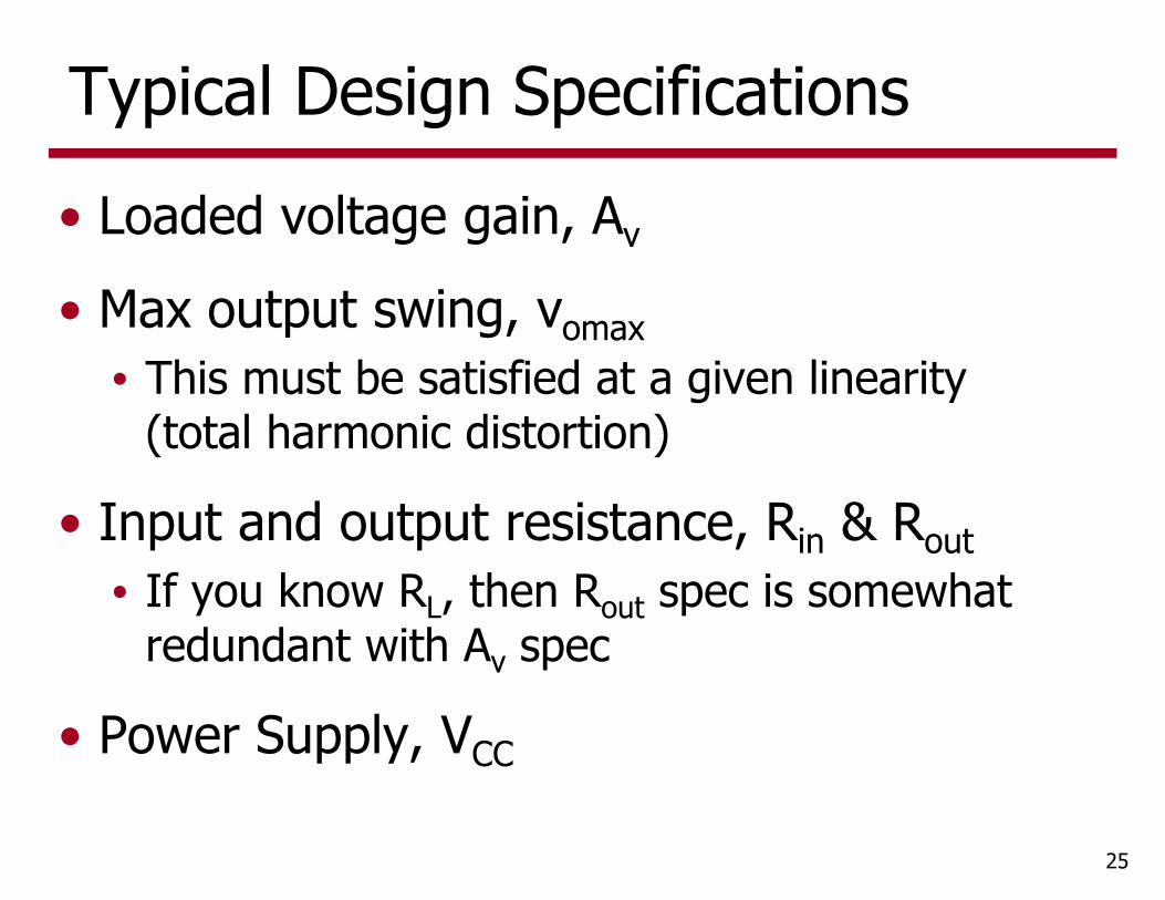
Typical Design Specifications
3
• Loaded voltage gain, Av
• Max output swing, vomax• This must be satisfied at a given linearity
(total harmonic distortion)
• Input and output resistance, Rin & Rout
• Power Supply, VCC

How to set DC Biasing Conditions?
4
• In order to meet all design specifications, the DC biasing conditions (IC, RC) must be set appropriately
• Can transform design specifications into functions of IC & RC and graph them to find acceptable solution space
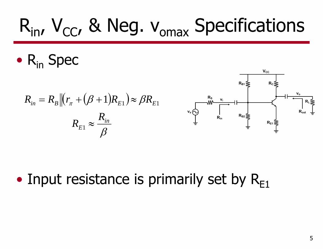
Rin, VCC, & Neg. vomax Specifications
5
• Rin Spec
inE
EEBin
RR
RRrRR
1
111
• Input resistance is primarily set by RE1

Rin, VCC, & Neg. vomax Specifications
6
• Need a minimum VCE to keep transistor in active mode with maximum negative swing
margin)design 200mV(w/ 500Set min mVVCE
mVRIvRIVV
RIvVRIV
EC
oCCCCCE
CCoCEEC
CC
5001maxmin
maxmin1
• VCC Spec (w/ max negative swing)
Rin, VCC, & Neg. vomax Specifications
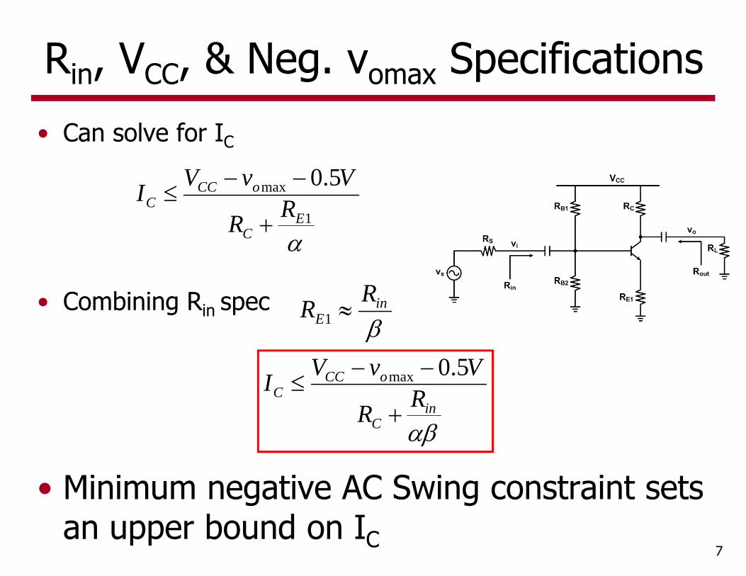
7
• Can solve for IC
• Combining Rin spec
1
max 5.0E
C
oCCC RR
VvVI
• Minimum negative AC Swing constraint sets an upper bound on IC
in
ERR 1
in
C
oCCC RR
VvVI
5.0max
Pos. vomax Specification
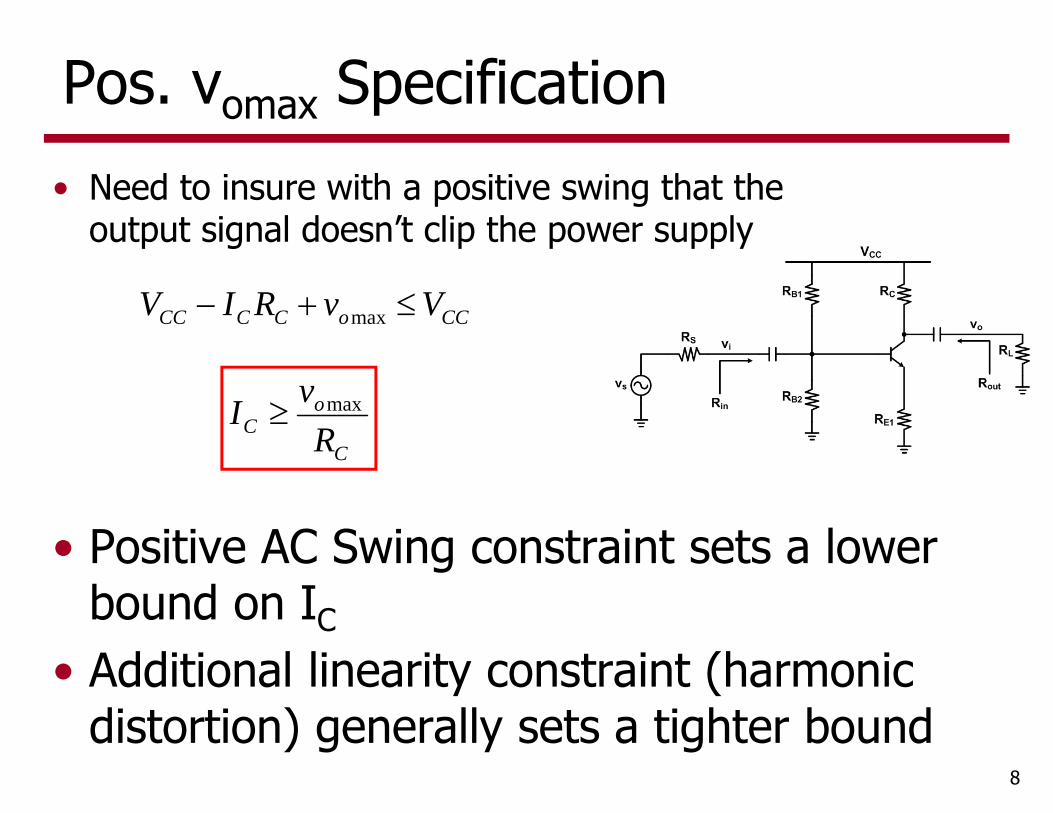
8
• Need to insure with a positive swing that the output signal doesn’t clip the power supply
CCoCCCC VvRIV max
• Positive AC Swing constraint sets a lower bound on IC
• Additional linearity constraint (harmonic distortion) generally sets a tighter bound
C
oC R
vI max

Gain Specification
9
11 11 E
th
C
LCth
C
Em
LCm
i
ov R
VI
RRVI
RgRRg
vvA
• Gain constraint sets a lower bound on IC
inv
LC
thv
EvLC
thvC RA
RR
VARA
RR
VAI
1
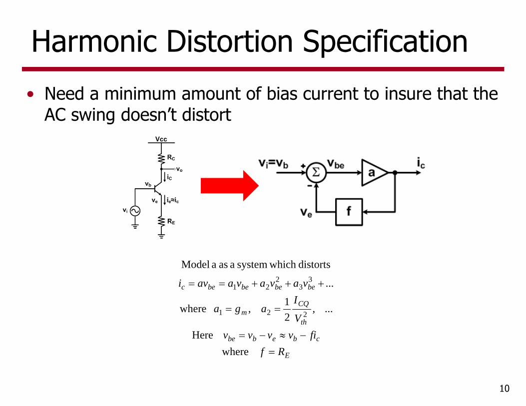
Harmonic Distortion Specification
10
• Need a minimum amount of bias current to insure that the AC swing doesn’t distort
E
cbebbe
th
CQm
bebebebec
Rffivvvv
V
Iaga
vavavaavi
where Here
... ,21 , where
...
distorts which system a as a Model
221
33
221
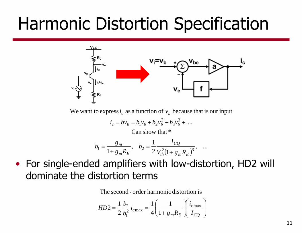
Harmonic Distortion Specification
11
... ,
121 ,
1
* thatshowCan ....
inputour is that because offunction a as express want toWe
3221
33
221
Emth
CQ
Em
m
bbbbc
bc
RgV
Ib
Rgg
b
vbvbvbbvi
vi
CQ
c
Emc I
iRg
ibbHD max
max21
2
11
41
212
is distortion harmonicorder -second The
• For single-ended amplifiers with low-distortion, HD2 will dominate the distortion terms
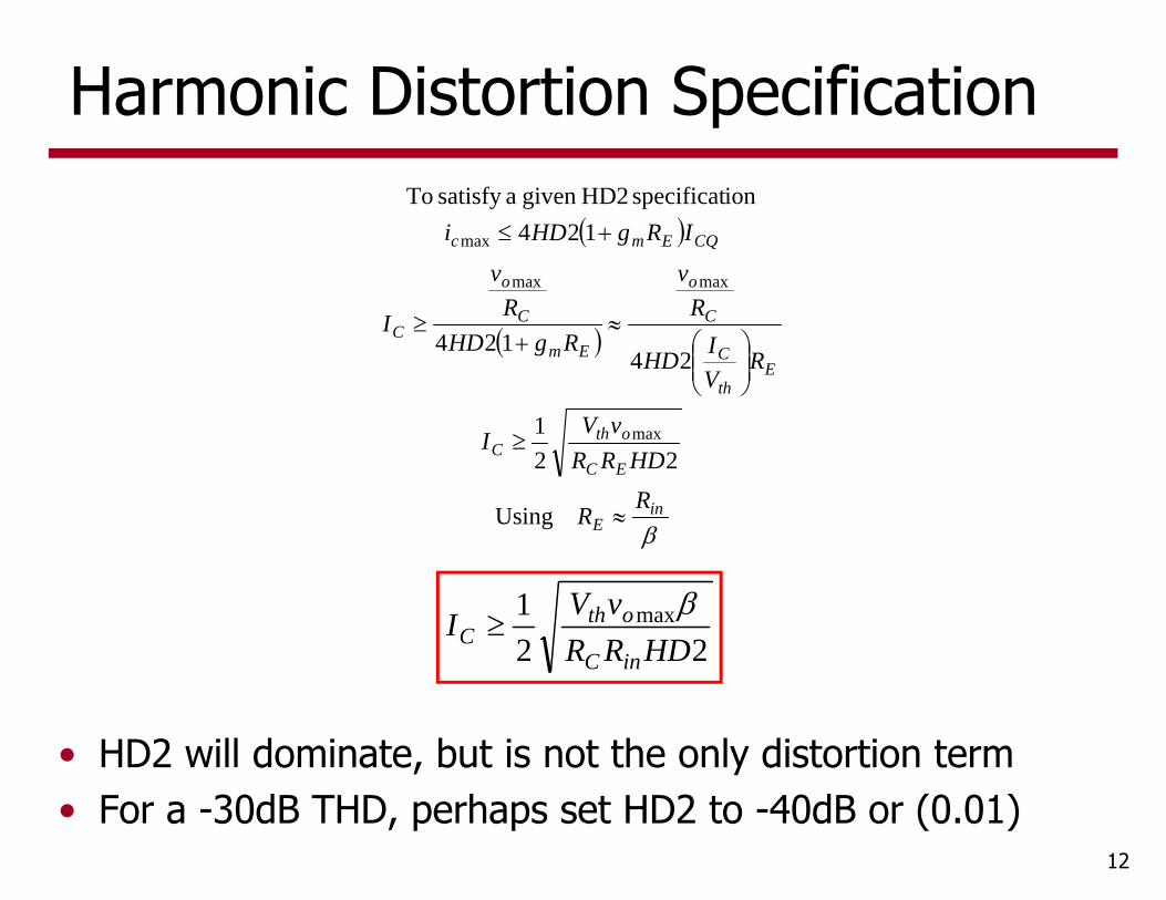
Harmonic Distortion Specification
12
221 max
HDRRvV
IinC
othC
in
E
EC
othC
Eth
C
C
o
Em
C
o
C
CQEmc
RR
HDRRvV
I
RVIHD
Rv
RgHDR
v
I
IRgHDi
Using
221
24124
124ionspecificat HD2given asatisfy To
max
maxmax
max
• HD2 will dominate, but is not the only distortion term• For a -30dB THD, perhaps set HD2 to -40dB or (0.01)

Output Resistance Specification
13
• Neglecting transistor output resistance, Rout is determined by RC
specoutC RR ,

Key CE Amp Design Equation Summary
14
specoutC
inC
othC
invLC
thvC
C
oC
inC
oCCC
RRHDRR
vVI
RARR
VAI
Rv
I
RR
VvVI
,
max
max
maxCC
:ResistanceOutput 22
1 :Distortion Harmonic
:Gain
:Swing Pos.
5.0 :V Rin, Swing, Neg.
Design Example - Specifications
15
• |Av| |-8|
• Rin 200k
• Rout ≤ 30k
• Vomax = 20mVpk w/ THD ≤ -30dB
• VCC = 5V
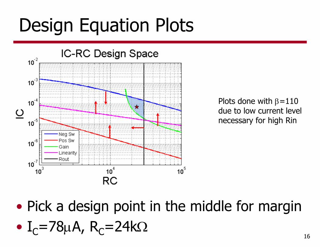
Design Equation Plots
16
• Pick a design point in the middle for margin• IC=78A, RC=24k
Plots done with =110 due to low current level necessary for high Rin
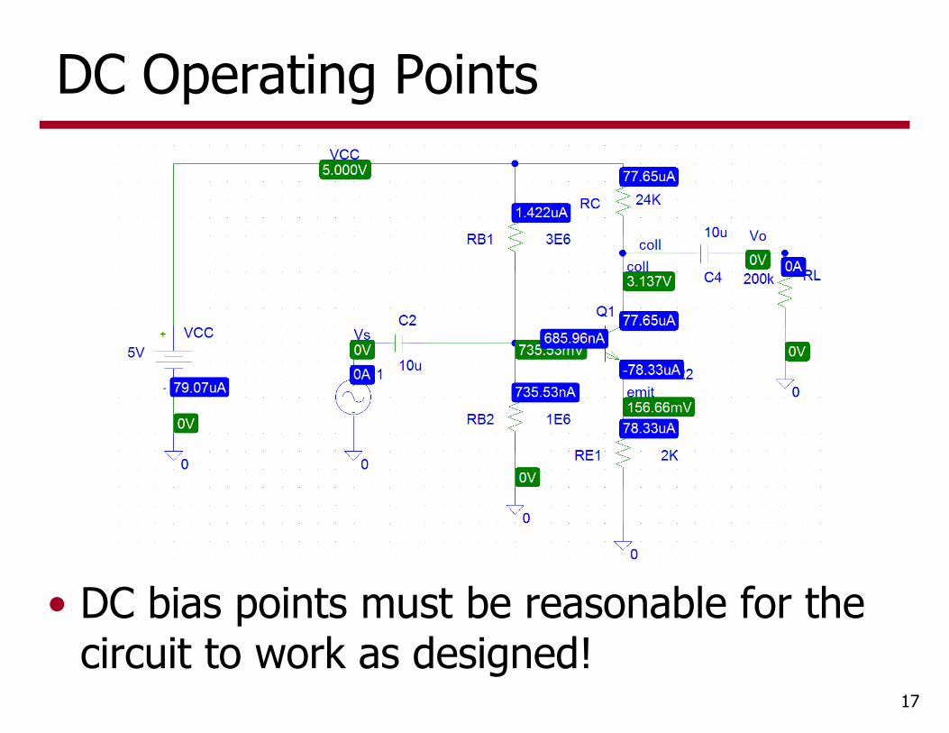
DC Operating Points
17
• DC bias points must be reasonable for the circuit to work as designed!
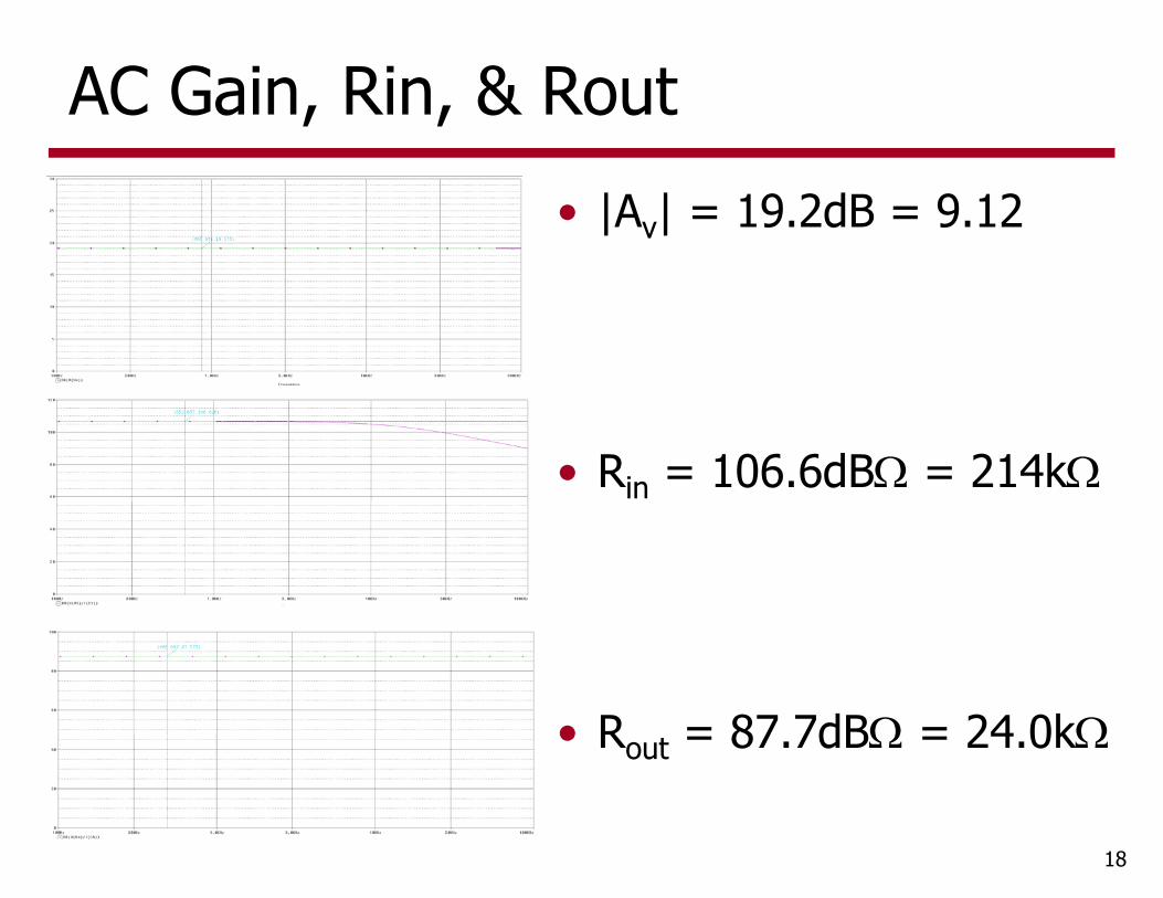
AC Gain, Rin, & Rout
18
• |Av| = 19.2dB = 9.12
• Rin = 106.6dB = 214k
• Rout = 87.7dB = 24.0k
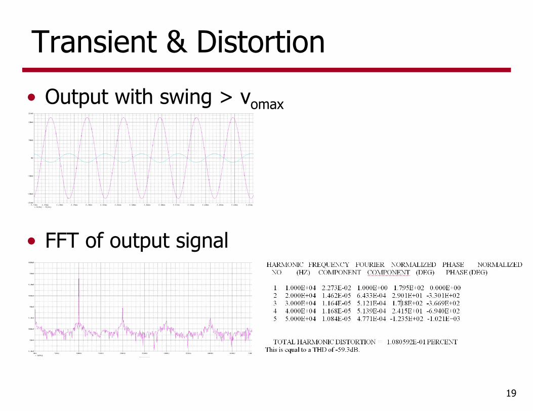
Transient & Distortion
19
• Output with swing > vomax
• FFT of output signal
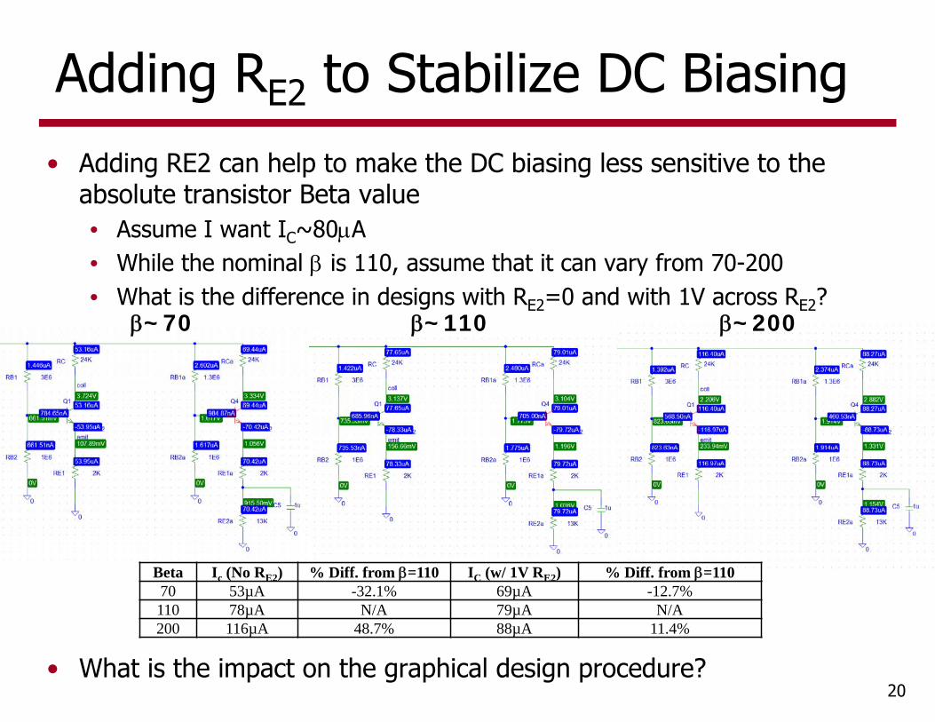
Adding RE2 to Stabilize DC Biasing
20
Beta Ic (No RE2) % Diff. from =110 IC (w/ 1V RE2) % Diff. from =11070 53µA -32.1% 69µA -12.7%110 78µA N/A 79µA N/A200 116µA 48.7% 88µA 11.4%
• Adding RE2 can help to make the DC biasing less sensitive to the absolute transistor Beta value• Assume I want IC~80A• While the nominal is 110, assume that it can vary from 70-200• What is the difference in designs with RE2=0 and with 1V across RE2?
~70 ~110 ~200
• What is the impact on the graphical design procedure?

Rin, VCC, & Neg. vomax Specs w/ RE2
21
• The only equation impacted is the Neg. vomax
• Need a minimum VCE to keep transistor in active mode with maximum negative swing
margin)design 200mV(w/ 500Set min mVVCE
mVRIRIvRIVV
RIvVRRIV
EEEC
oCCCCCE
CCoCEEEC
CC
50021maxmin
maxmin21
• VCC Spec (w/ max negative swing)
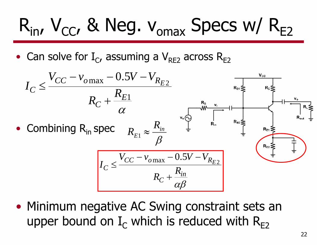
22
• Can solve for IC, assuming a VRE2 across RE2
• Combining Rin spec
1
max 25.0
EC
RoCCC RR
VVvVI E
• Minimum negative AC Swing constraint sets an upper bound on IC which is reduced with RE2
in
ERR 1
in
C
RoCCC RR
VVvVI E
2
5.0max
Rin, VCC, & Neg. vomax Specs w/ RE2
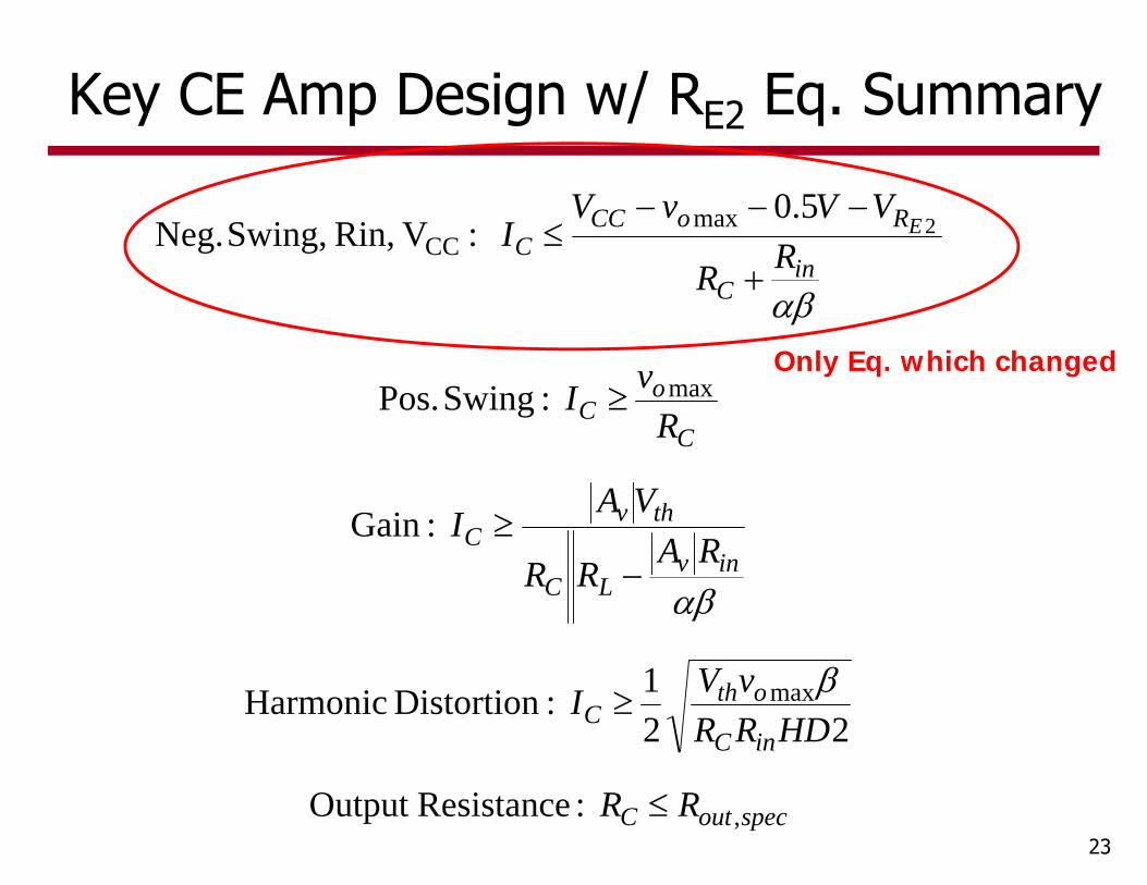
Key CE Amp Design w/ RE2 Eq. Summary
23specoutC
inC
othC
invLC
thvC
C
oC
inC
RoCCC
RR
HDRRvVI
RARR
VAI
RvI
RR
VVvVI E
,
max
max
maxCC
:ResistanceOutput
221 :Distortion Harmonic
:Gain
:Swing Pos.
5.0 :V Rin, Swing, Neg. 2
Only Eq. which changed
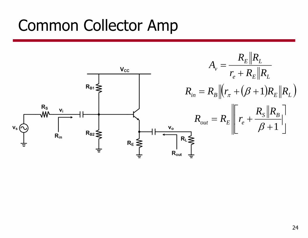
Common Collector Amp
24
1
1
BSeEout
LEBin
LEe
LEv
RRrRR
RRrRR
RRrRR
A
Typical Design Specifications
25
• Loaded voltage gain, Av
• Max output swing, vomax• This must be satisfied at a given linearity
(total harmonic distortion)
• Input and output resistance, Rin & Rout• If you know RL, then Rout spec is somewhat
redundant with Av spec
• Power Supply, VCC

How to set DC Biasing Conditions?
26
• In order to meet all design specifications, the DC biasing conditions (IE, RE) must be set appropriately
• Can transform design specifications into functions of IE & RE and graph them to find acceptable solution space
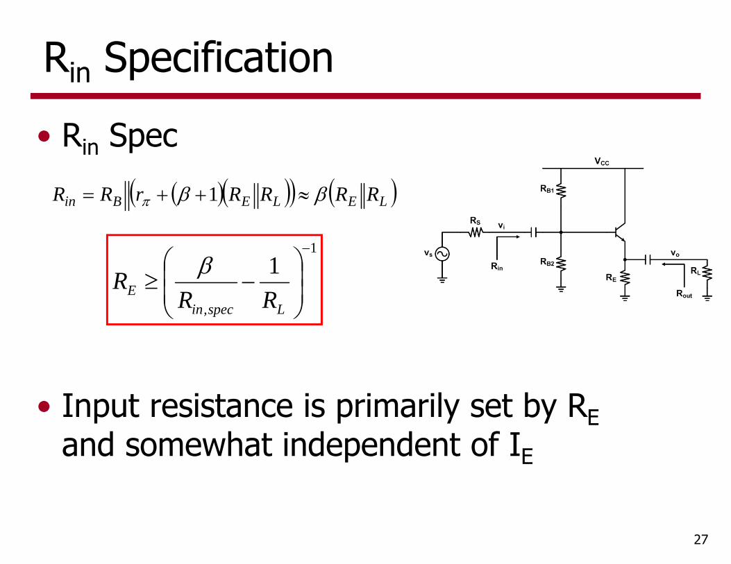
Rin Specification
27
• Rin Spec
• Input resistance is primarily set by REand somewhat independent of IE
LELEBin RRRRrRR 1
1
,
1
LspecinE RR
R

Neg. vomax Specification
28
• Need to insure with a negative swing that the output signal doesn’t clip the power supply
VvRI oEE 0max
• Negative AC Swing constraint sets a lower bound on IE
• Additional linearity constraint (harmonic distortion) generally sets a tighter bound
E
oE R
vI max
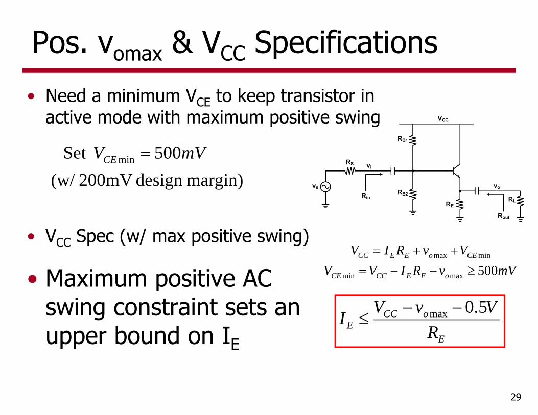
Pos. vomax & VCC Specifications
29
• Need a minimum VCE to keep transistor in active mode with maximum positive swing
margin)design 200mV(w/ 500Set min mVVCE
mVvRIVVVvRIV
oEECCCE
CEoEECC
500maxmin
minmax
• VCC Spec (w/ max positive swing)
E
oCCE R
VvVI 5.0max
• Maximum positive AC swing constraint sets an upper bound on IE

Gain Specification
30
• Gain constraint sets a lower bound on IE
vLE
thvE ARR
VAI
1
LEE
th
LE
LEe
LEv
RRIV
RRRRr
RRA
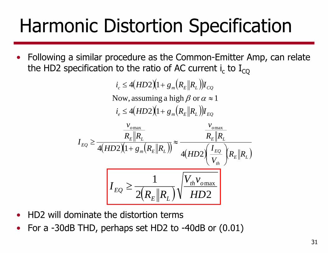
Harmonic Distortion Specification
31
• Following a similar procedure as the Common-Emitter Amp, can relate the HD2 specification to the ratio of AC current ic to ICQ
LEth
EQ
LE
o
LEm
LE
o
EQ
EQLEme
CQLEmc
RRVI
HD
RRv
RRgHDRR
v
I
IRRgHDi
IRRgHDi
24124
1241or high a assuming Now,
124
maxmax
221 max
HDvV
RRI oth
LEEQ
• HD2 will dominate the distortion terms• For a -30dB THD, perhaps set HD2 to -40dB or (0.01)
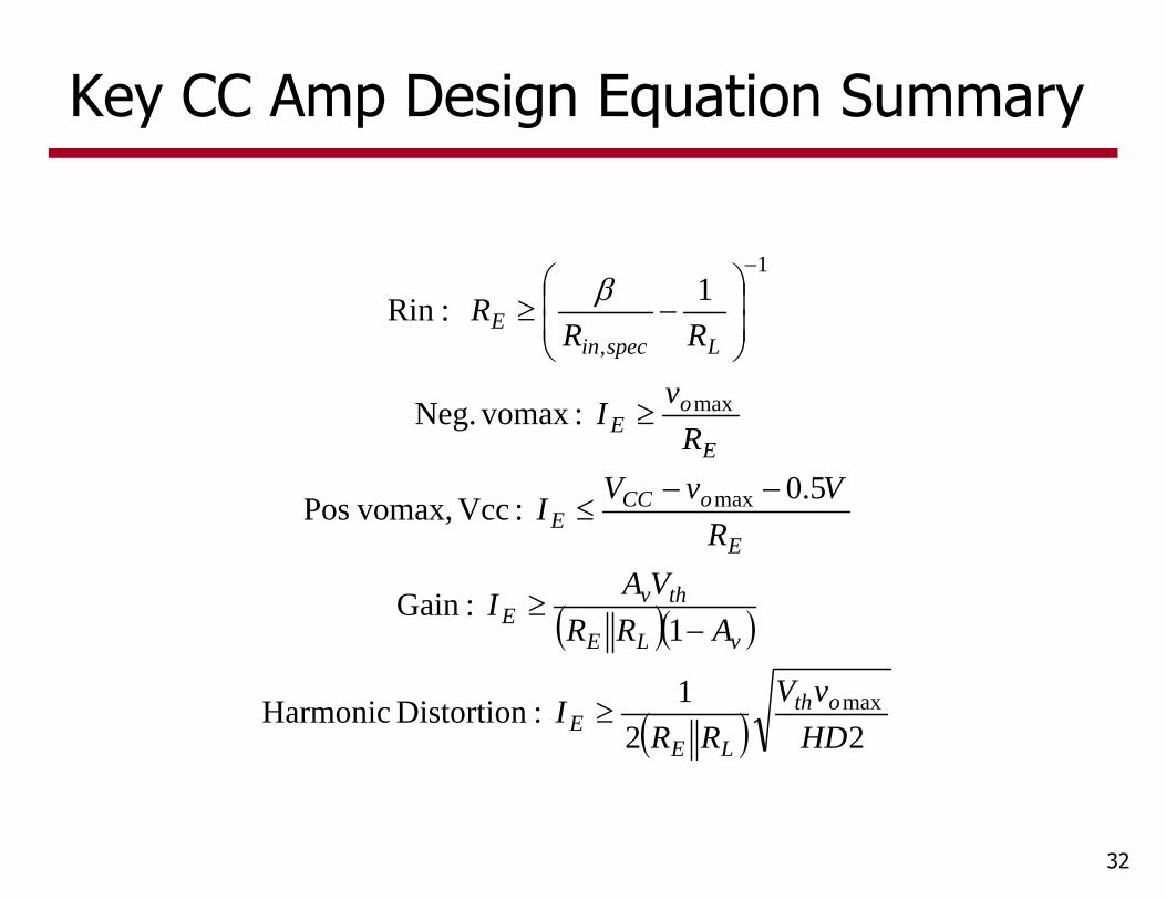
Key CC Amp Design Equation Summary
32
221 :Distortion Harmonic
1 :Gain
5.0 :Vcc vomax,Pos
: vomaxNeg.
1 :Rin
max
max
max
1
,
HDvV
RRI
ARRVA
I
RVvV
I
Rv
I
RRR
oth
LEE
vLE
thvE
E
oCCE
E
oE
LspecinE

Design Example - Specifications
33
• Av 0.95
• Rin 1k
• Vomax = 500mVpk w/ THD ≤ -30dB• Here I set HD2=40dB or 0.01
• VCC = 5V
• RL = 50
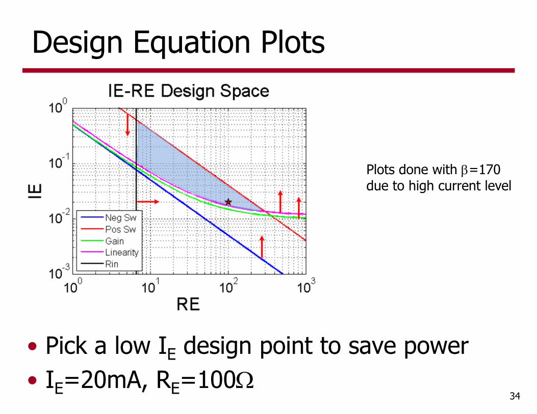
Design Equation Plots
34
• Pick a low IE design point to save power• IE=20mA, RE=100
Plots done with =170 due to high current level
DC Operating Points
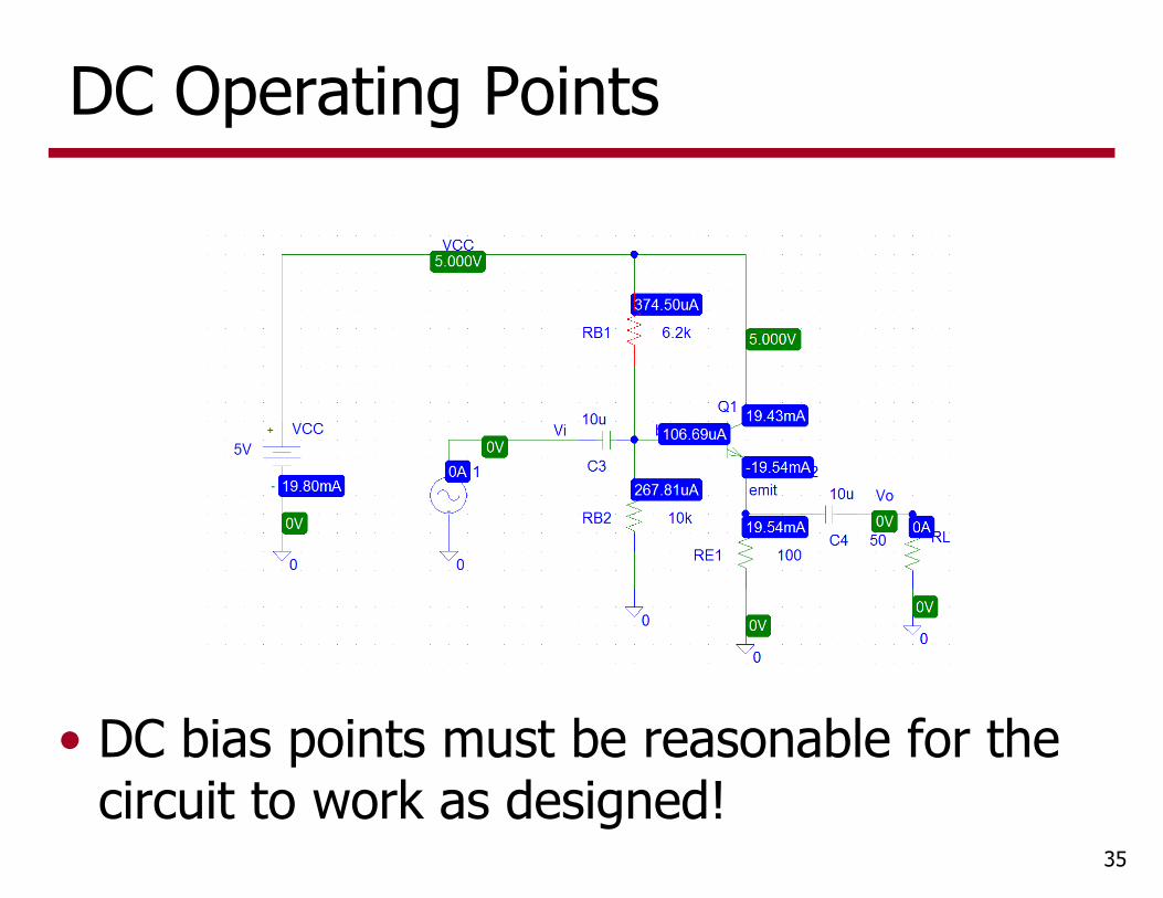
35
• DC bias points must be reasonable for the circuit to work as designed!
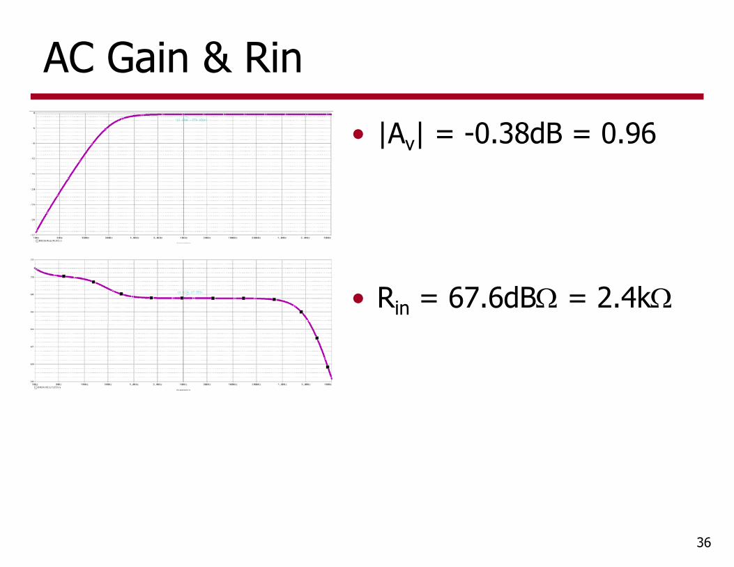
AC Gain & Rin
36
• |Av| = -0.38dB = 0.96
• Rin = 67.6dB = 2.4k
Transient & Distortion
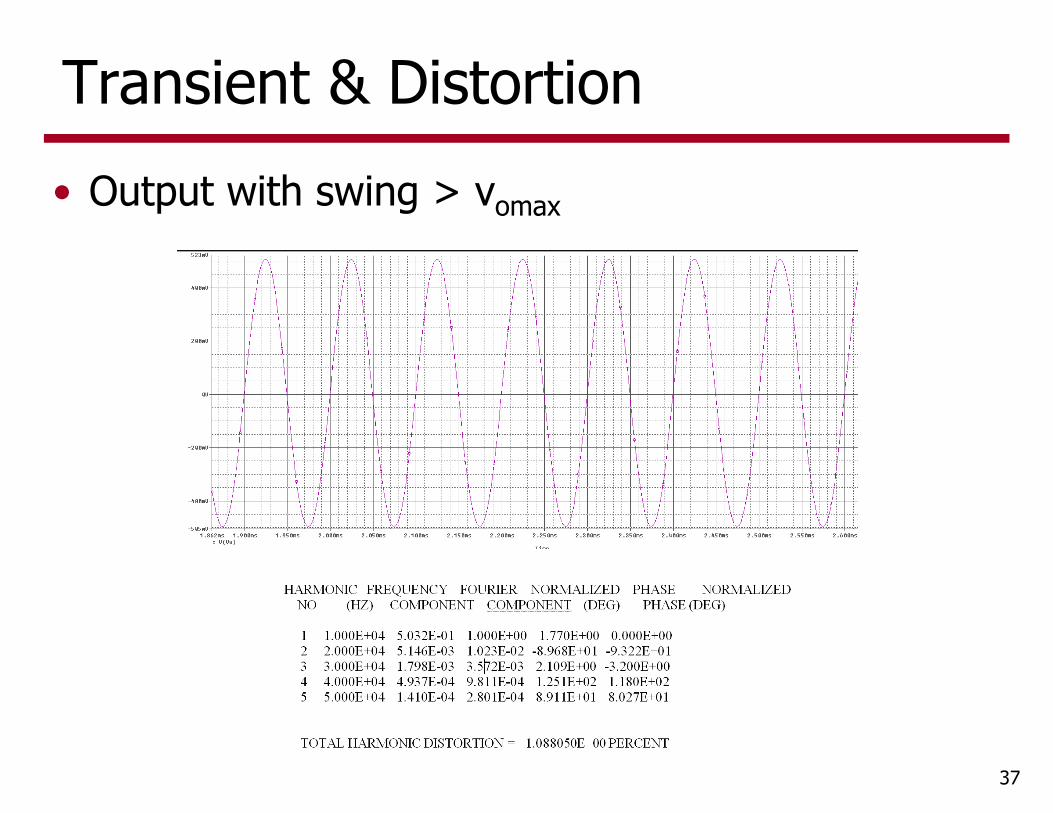
37
• Output with swing > vomax


![ECEN325: Electronics Spring 2020ece.tamu.edu/~spalermo/ecen325/semiconductor_diode.pdfS [Sedra/Smith] Reverse Breakdown 9 • For large negative voltages, the previous exponential](https://img.dokumen.tips/doc/110x75/6087cd4ea5513d364f132584/ecen325-electronics-spring-spalermoecen325semiconductordiodepdf-s-sedrasmith.jpg)