Embed Size (px)
Citation preview
Material derived from http://en.wikipedia.org/wiki/DRAM and Micron Technology, Inc. Data Sheet for the MT48LC32M8A2 – 8 Meg x 8 x 4 banks, PDF: 09005aef8091e6d1, 256Mb_sdr.pdf - Rev. N 1/10 EN, 1999.
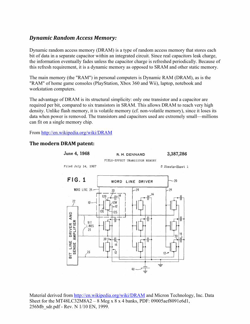
DynamicRandomAccessMemory:
Dynamic random access memory (DRAM) is a type of random access memory that stores each bit of data in a separate capacitor within an integrated circuit. Since real capacitors leak charge, the information eventually fades unless the capacitor charge is refreshed periodically. Because of this refresh requirement, it is a dynamic memory as opposed to SRAM and other static memory.
The main memory (the "RAM") in personal computers is Dynamic RAM (DRAM), as is the "RAM" of home game consoles (PlayStation, Xbox 360 and Wii), laptop, notebook and workstation computers.
The advantage of DRAM is its structural simplicity: only one transistor and a capacitor are required per bit, compared to six transistors in SRAM. This allows DRAM to reach very high density. Unlike flash memory, it is volatile memory (cf. non-volatile memory), since it loses its data when power is removed. The transistors and capacitors used are extremely small—millions can fit on a single memory chip.
From http://en.wikipedia.org/wiki/DRAM
ThemodernDRAMpatent:
Material derived from http://en.wikipedia.org/wiki/DRAM and Micron Technology, Inc. Data Sheet for the MT48LC32M8A2 – 8 Meg x 8 x 4 banks, PDF: 09005aef8091e6d1, 256Mb_sdr.pdf - Rev. N 1/10 EN, 1999.
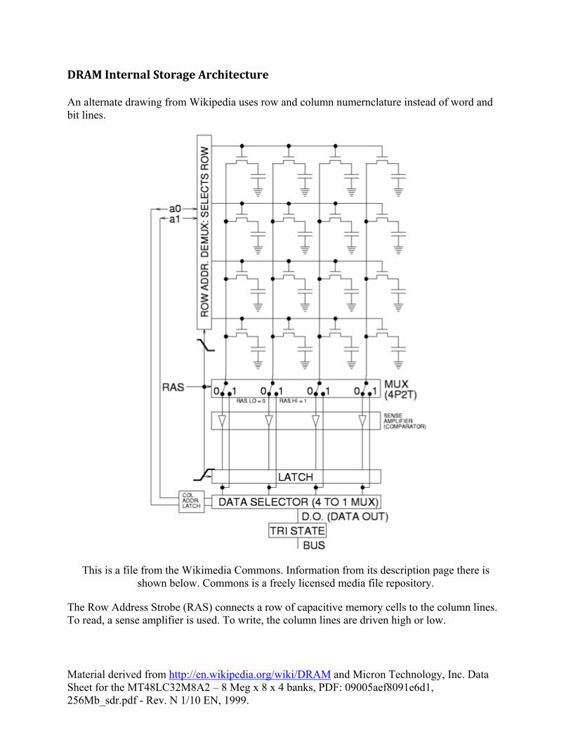
DRAMInternalStorageArchitecture
An alternate drawing from Wikipedia uses row and column numernclature instead of word and bit lines.
This is a file from the Wikimedia Commons. Information from its description page there is shown below. Commons is a freely licensed media file repository.
The Row Address Strobe (RAS) connects a row of capacitive memory cells to the column lines. To read, a sense amplifier is used. To write, the column lines are driven high or low.
Material derived from http://en.wikipedia.org/wiki/DRAM and Micron Technology, Inc. Data Sheet for the MT48LC32M8A2 – 8 Meg x 8 x 4 banks, PDF: 09005aef8091e6d1, 256Mb_sdr.pdf - Rev. N 1/10 EN, 1999.
When an external Column Address Strobe (CAS) follows the RAS, the sense amplifier value is captured. Then, when the CAS remains low, the output of the sense amp is fed back to the columns to “refresh” the row being read.
Therefore, RAS followd by CAS or RAS before CAS leads to a read function (or write if desired).
If no access is performed, an external refresh cycle musted be initiated. The normal way of doing a refresh is to present CAS before RAS, a sequence not associated with a normal read or write cycle.
DRAMFlavors
DRAM
Fast Page Mode DRAM
Extended Data Output DRAM
Burst EDO DRAM
Multibank DRAM
Synchronous DRAM (SDRAM)
Pseudo Statc DRAM (PSDRAM)
Double Data Rate (DDR)
Comments
Historically, DRAMs can come and go in as little as 6 months … first released to obsolete.
DRAMs often have “extra bits” for parity error detection or full error detection and correction.
DRAM data storage can be effected by temperature and electro magnetic effects.
Dr. Grantmer’s DRAM Notes P. 137-159.
Material derived from http://en.wikipedia.org/wiki/DRAM and Micron Technology, Inc. Data Sheet for the MT48LC32M8A2 – 8 Meg x 8 x 4 banks, PDF: 09005aef8091e6d1, 256Mb_sdr.pdf - Rev. N 1/10 EN, 1999.
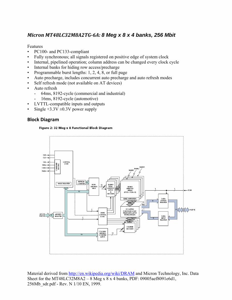
MicronMT48LC32M8A2TG‐6A:8 Meg x 8 x 4 banks, 256 Mbit
Features • PC100- and PC133-compliant • Fully synchronous; all signals registered on positive edge of system clock • Internal, pipelined operation; column address can be changed every clock cycle • Internal banks for hiding row access/precharge • Programmable burst lengths: 1, 2, 4, 8, or full page • Auto precharge, includes concurrent auto precharge and auto refresh modes • Self refresh mode (not available on AT devices) • Auto refresh
- 64ms, 8192-cycle (commercial and industrial) - 16ms, 8192-cycle (automotive)
• LVTTL-compatible inputs and outputs • Single +3.3V ±0.3V power supply
Block Diagram
Material derived from http://en.wikipedia.org/wiki/DRAM and Micron Technology, Inc. Data Sheet for the MT48LC32M8A2 – 8 Meg x 8 x 4 banks, PDF: 09005aef8091e6d1, 256Mb_sdr.pdf - Rev. N 1/10 EN, 1999.
Pinout
Functional Description
In general, 256Mb SDRAM devices (16 Meg x 4 x 4 banks, 8 Meg x 8 x 4 banks, and 4 Meg x 16 x 4 banks) are quad-bank DRAM that operate at 3.3V and include a synchronous interface. All signals are registered on the positive edge of the clock signal, CLK. Each of the x4’s 67,108,864-bit banks is organized as 8192 rows by 2048 columns by 4 bits. Each of the x8’s 67,108,864-bit banks is organized as 8192 rows by 1024 columns by 8 bits. Each of the x16’s 67,108,864-bit banks is organized as 8192 rows by 512 columns by 16 bits.
Read and write accesses to the SDRAM are burst-oriented; accesses start at a selected location and continue for a programmed number of locations in a programmed sequence.
Accesses begin with the registration of an ACTIVE command, followed by a READ or WRITE command. The address bits registered coincident with the ACTIVE command are used to select the bank and row to be accessed (BA0 and BA1 select the bank, A[12:0] select the row). The address bits (x4: A[9:0], A11; x8: A[9:0]; x16: A[8:0]) registered coincident with the READ or WRITE command are used to select the starting column location for the burst access.
Prior to normal operation, the SDRAM must be initialized. The following sections provide detailed information covering device initialization, register definition, command descriptions, and device operation.
Material derived from http://en.wikipedia.org/wiki/DRAM and Micron Technology, Inc. Data Sheet for the MT48LC32M8A2 – 8 Meg x 8 x 4 banks, PDF: 09005aef8091e6d1, 256Mb_sdr.pdf - Rev. N 1/10 EN, 1999.
Pin Descriptions
Addressing
Each of the x8’s 67,108,864-bit banks is organized as 8192 rows by 1024 columns by 8 bits.
- Initial A[12:0] (RAS period) addresses one of the 8192 rows - Initial BA[1:0] (RAS period) addresses one of the four banks - Later A[9:0] (CAS period) addresses one of the 1024 columns
Material derived from http://en.wikipedia.org/wiki/DRAM and Micron Technology, Inc. Data Sheet for the MT48LC32M8A2 – 8 Meg x 8 x 4 banks, PDF: 09005aef8091e6d1, 256Mb_sdr.pdf - Rev. N 1/10 EN, 1999.
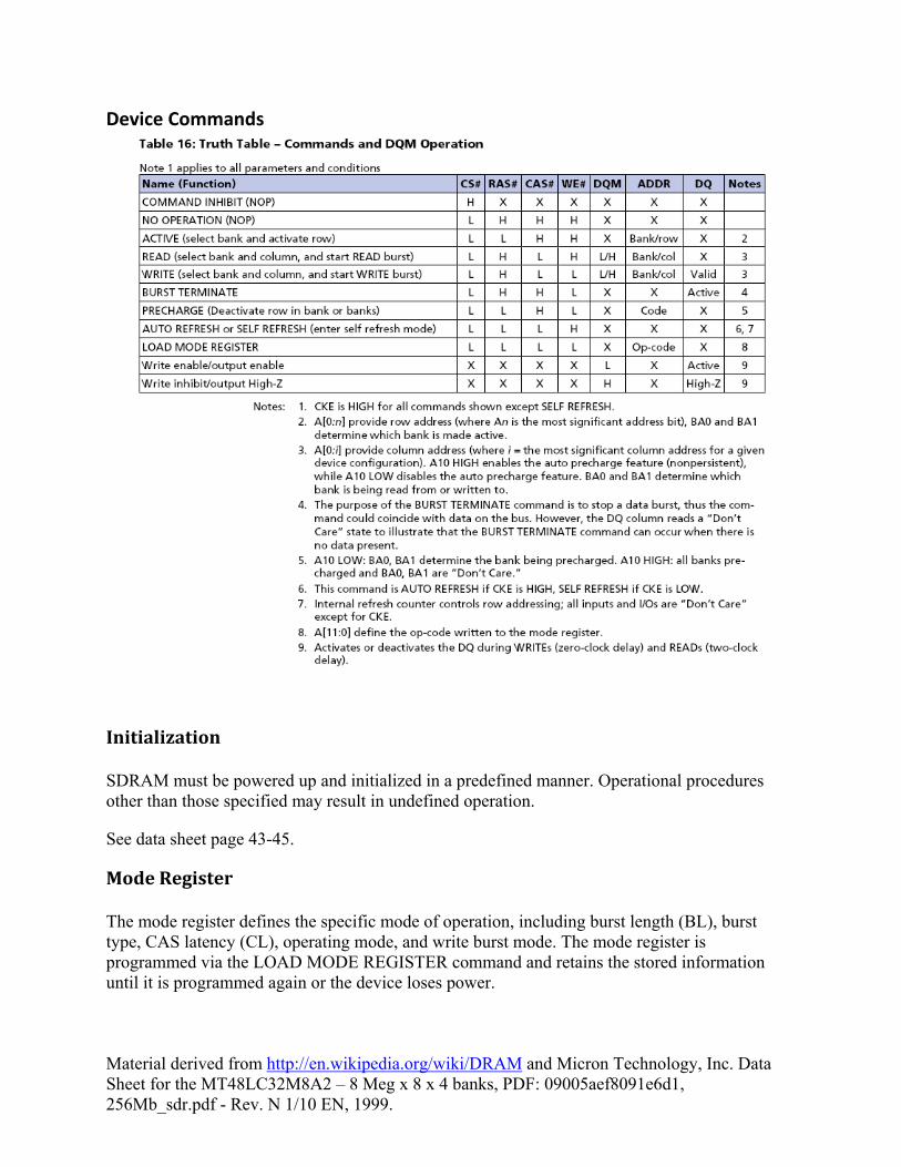
Device Commands
Initialization
SDRAM must be powered up and initialized in a predefined manner. Operational procedures other than those specified may result in undefined operation.
See data sheet page 43-45.
ModeRegister
The mode register defines the specific mode of operation, including burst length (BL), burst type, CAS latency (CL), operating mode, and write burst mode. The mode register is programmed via the LOAD MODE REGISTER command and retains the stored information until it is programmed again or the device loses power.
Material derived from http://en.wikipedia.org/wiki/DRAM and Micron Technology, Inc. Data Sheet for the MT48LC32M8A2 – 8 Meg x 8 x 4 banks, PDF: 09005aef8091e6d1, 256Mb_sdr.pdf - Rev. N 1/10 EN, 1999.
SimpleExecution
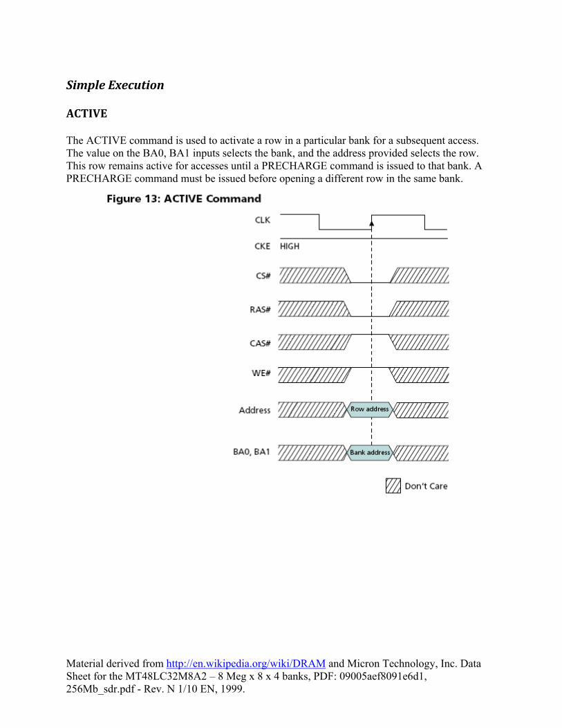
ACTIVE
The ACTIVE command is used to activate a row in a particular bank for a subsequent access. The value on the BA0, BA1 inputs selects the bank, and the address provided selects the row. This row remains active for accesses until a PRECHARGE command is issued to that bank. A PRECHARGE command must be issued before opening a different row in the same bank.
Material derived from http://en.wikipedia.org/wiki/DRAM and Micron Technology, Inc. Data Sheet for the MT48LC32M8A2 – 8 Meg x 8 x 4 banks, PDF: 09005aef8091e6d1, 256Mb_sdr.pdf - Rev. N 1/10 EN, 1999.
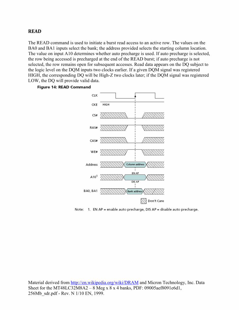
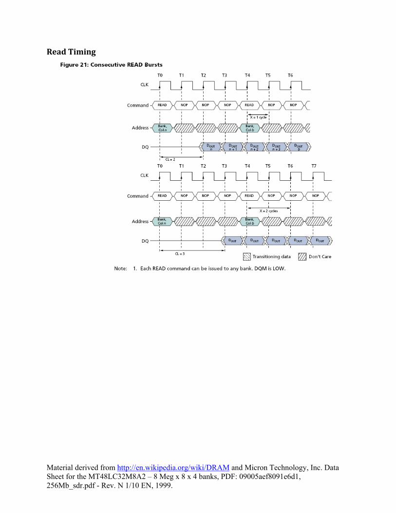
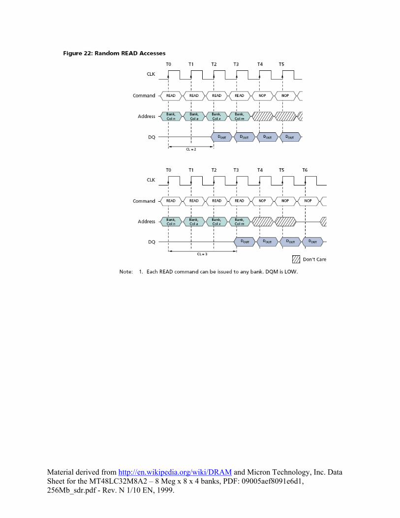
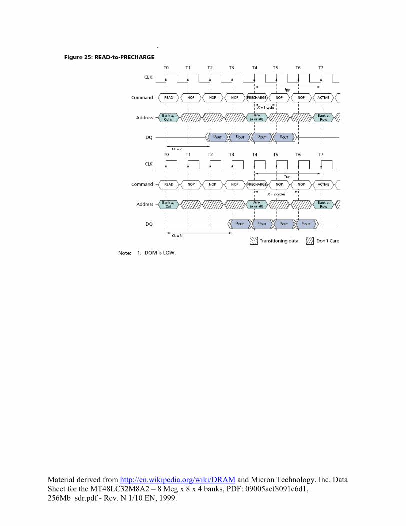
READ
The READ command is used to initiate a burst read access to an active row. The values on the BA0 and BA1 inputs select the bank; the address provided selects the starting column location. The value on input A10 determines whether auto precharge is used. If auto precharge is selected, the row being accessed is precharged at the end of the READ burst; if auto precharge is not selected, the row remains open for subsequent accesses. Read data appears on the DQ subject to the logic level on the DQM inputs two clocks earlier. If a given DQM signal was registered HIGH, the corresponding DQ will be High-Z two clocks later; if the DQM signal was registered LOW, the DQ will provide valid data.

Material derived from http://en.wikipedia.org/wiki/DRAM and Micron Technology, Inc. Data Sheet for the MT48LC32M8A2 – 8 Meg x 8 x 4 banks, PDF: 09005aef8091e6d1, 256Mb_sdr.pdf - Rev. N 1/10 EN, 1999.
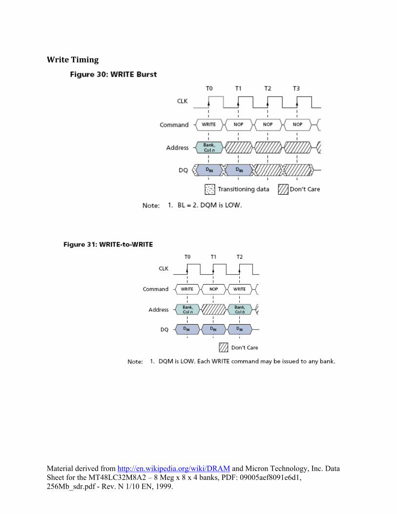
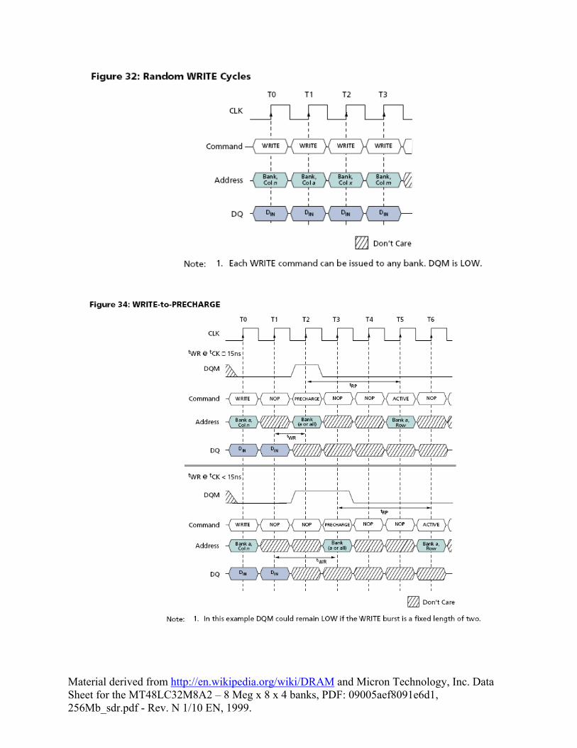
WRITE
The WRITE command is used to initiate a burst write access to an active row. The values on the BA0 and BA1 inputs select the bank; the address provided selects the starting column location. The value on input A10 determines whether auto precharge is used. If auto precharge is selected, the row being accessed is precharged at the end of the write burst; if auto precharge is not selected, the row remains open for subsequent accesses. Input data appearing on the DQ is written to the memory array, subject to the DQM input logic level appearing coincident with the data. If a given DQM signal is registered LOW, the corresponding data is written to memory; if the DQM signal is registered HIGH, the corresponding data inputs are ignored and a WRITE is not executed to that byte/column location.

Material derived from http://en.wikipedia.org/wiki/DRAM and Micron Technology, Inc. Data Sheet for the MT48LC32M8A2 – 8 Meg x 8 x 4 banks, PDF: 09005aef8091e6d1, 256Mb_sdr.pdf - Rev. N 1/10 EN, 1999.
PRECHARGE
The PRECHARGE command is used to deactivate the open row in a particular bank or the open row in all banks. The bank(s) will be available for a subsequent row access a specified time (tRP) after the PRECHARGE command is issued. Input A10 determines whether one or all banks are to be precharged, and in the case where only one bank is precharged, inputs BA0 and BA1 select the bank. Otherwise BA0 and BA1 are treated as “Don’t Care.” After a bank has been precharged, it is in the idle state and must be activated prior to any READ or WRITE commands are issued to that bank.
Material derived from http://en.wikipedia.org/wiki/DRAM and Micron Technology, Inc. Data Sheet for the MT48LC32M8A2 – 8 Meg x 8 x 4 banks, PDF: 09005aef8091e6d1, 256Mb_sdr.pdf - Rev. N 1/10 EN, 1999.
AUTOREFRESH
AUTO REFRESH is used during normal operation of the SDRAM and is analogous to CAS#-BEFORE-RAS# (CBR) refresh in conventional DRAMs. This command is nonpersistent, so it must be issued each time a refresh is required. All active banks must be precharged prior to issuing an AUTO REFRESH command. The AUTO REFRESH command should not be issued until the minimum tRP has been met after the PRECHARGE command, as shown in Bank/Row Activation (page 51 of the data sheet). The addressing is generated by the internal refresh controller. This makes the address bits a “Don’t Care” during an AUTO REFRESH command.
Regardless of device width, the 256Mb SDRAM requires 8192 AUTO REFRESH cycles every 64ms (commercial and industrial) or 16ms (automotive). Providing a distributed AUTO REFRESH command every 7.813μs (commercial and industrial) or 1.953μs (automotive) will meet the refresh requirement and ensure that each row is refreshed. Alternatively, 8192 AUTO REFRESH commands can be issued in a burst at the minimum cycle rate (tRFC), once every 64ms (commercial and industrial) or 16ms (automotive).
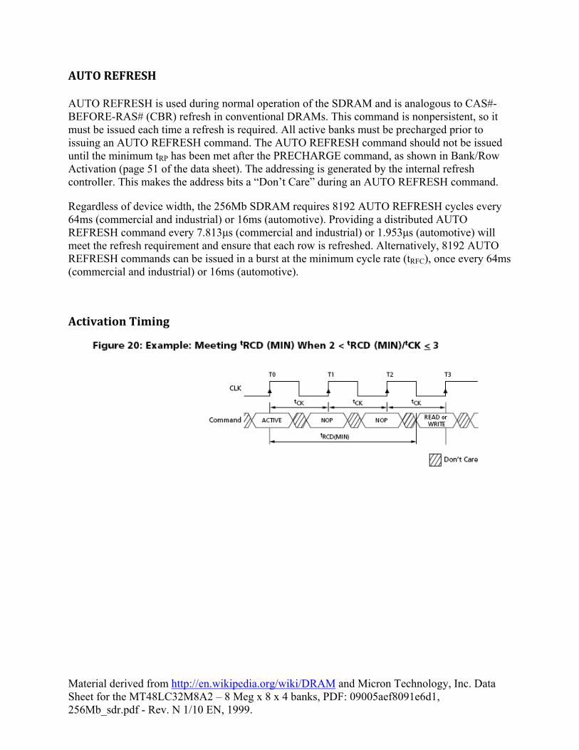
ActivationTiming
Material derived from http://en.wikipedia.org/wiki/DRAM and Micron Technology, Inc. Data Sheet for the MT48LC32M8A2 – 8 Meg x 8 x 4 banks, PDF: 09005aef8091e6d1, 256Mb_sdr.pdf - Rev. N 1/10 EN, 1999.
ReadTiming
Material derived from http://en.wikipedia.org/wiki/DRAM and Micron Technology, Inc. Data Sheet for the MT48LC32M8A2 – 8 Meg x 8 x 4 banks, PDF: 09005aef8091e6d1, 256Mb_sdr.pdf - Rev. N 1/10 EN, 1999.
Material derived from http://en.wikipedia.org/wiki/DRAM and Micron Technology, Inc. Data Sheet for the MT48LC32M8A2 – 8 Meg x 8 x 4 banks, PDF: 09005aef8091e6d1, 256Mb_sdr.pdf - Rev. N 1/10 EN, 1999.
Material derived from http://en.wikipedia.org/wiki/DRAM and Micron Technology, Inc. Data Sheet for the MT48LC32M8A2 – 8 Meg x 8 x 4 banks, PDF: 09005aef8091e6d1, 256Mb_sdr.pdf - Rev. N 1/10 EN, 1999.
WriteTiming
Material derived from http://en.wikipedia.org/wiki/DRAM and Micron Technology, Inc. Data Sheet for the MT48LC32M8A2 – 8 Meg x 8 x 4 banks, PDF: 09005aef8091e6d1, 256Mb_sdr.pdf - Rev. N 1/10 EN, 1999.