Embed Size (px)
Citation preview

11/29/2006 1
Dynamic LogicDynamic LogicCOEN 6511COEN 6511

11/29/2006 2
Dynamic Latch: Charge Dynamic Latch: Charge LeakageLeakage
Stored charge leaks away due to reverse-bias current.Stored value is good for about 1 ms.Value must be rewritten to be valid.If not loaded every cycle, must ensure that latch is loaded often enough to keep data valid.
Cd+Cg
D
Φ
X
X

11/29/2006 3
Dynamic LatchDynamic Latch--Operation Operation
Uses complementary transmission gate to ensure that storage node is always strongly driven.Latch is transparent when transmission gate is closed.Storage capacitance comes primarily from transmission gate diffusion capacitance and inverter gate capacitance.φ = 0: transmission gate is off, inverter output is determined bystorage node.φ = 1: transmission gate is on, inverter output follows D input.Setup and hold times determined by transmission gate—must ensure that value stored on transmission gate is solid.

11/29/2006 4
Dynamic LogicDynamic Logic• Dynamic Circuits will be introduced and
their performance in terms of power, area, delay, energy and AT2 will be reviewed.
• We will review the following logic families:• Domino logic• P-E logic• NORA logic• 2-phase logic• Multiple O/P domino logic• Cascode logic

11/29/2006 5
A brief introduction to Dynamic logic
• Dynamic logic• Steady-State Behavior of Dynamic
Logic• Performance of Dynamic Logic• Noise Considerations in Dynamic
Design

11/29/2006 6
General ConceptGeneral ConceptPrecharge and EvaluationPrecharge and Evaluation

11/29/2006 7
Dynamic Combinational Dynamic Combinational LogicLogic
Mp
Me
VDD
PDN
φ
In1In2In3
OutMe
Mp
VDD
PUN
φ
In1In2In3
φ
φ
Out
CL
CL
φp networkφn network
Precharge/ Evaluate Networks

11/29/2006 8
OUTPUT
A C
B
CLKCLK
OUTPUT Precharge Evaluation Precharge
Example of Dynamic Circuit

11/29/2006 9
Charge and dischargeCharge and discharge
Clock, ф
A
B
C
Output
11/29/2006 10
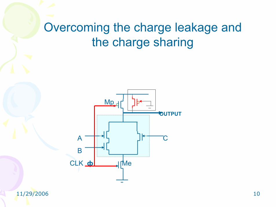
Mp OUTPUT
A C
B
CLK ф Me
Overcoming the charge leakage and the charge sharing

11/29/2006 11
Mp
Me
VDD
φ
Out
φ
A
B
C
• N + 1 Transistors
• Ratioless
• No Static Power Consumption
• Noise Margins small (NM L)
• Requires Clock
ExampleExample
11/29/2006 12
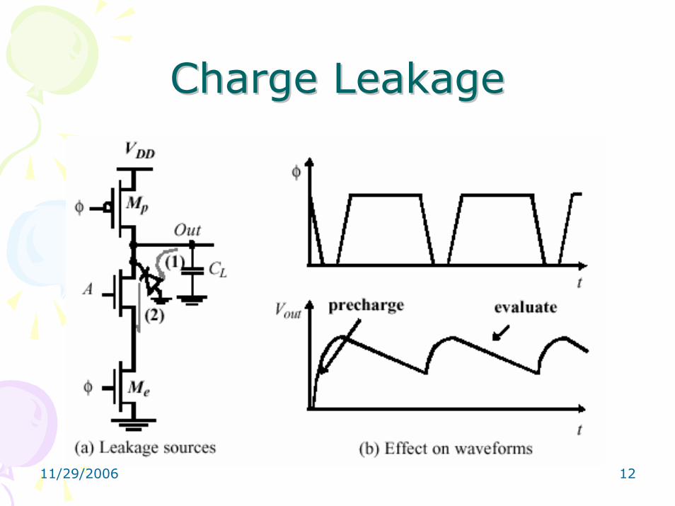
Charge LeakageCharge Leakage

11/29/2006 13
Charge SharingCharge Sharing

11/29/2006 14
Clock Feed throughClock Feed through

11/29/2006 15
Cascading Dynamic LogicCascading Dynamic Logic

11/29/2006 16
Transient ResponseTransient Response
0.00e+00 2.00e-09 4.00e-09 6.00e-09t (nsec)
0.0
2.0
4.0
6.0V
out(
Vol
t )
φ Vout
PRECHARGEEVALUATION
11/29/2006 17
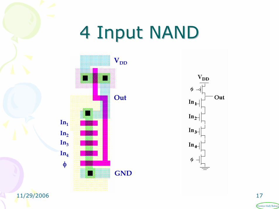
4 Input NAND4 Input NAND
In1
In2
In3
In4
Out
VDD
GNDφ
Prentice Hall/Rabaey

11/29/2006 18
Dynamic FlipDynamic Flip--Flop Flop
D Q
Φ Φ
Φ Φ
X Y
X
X
Y
Q
Φ
Φ
x

11/29/2006 19
P-E logic • Instead of using a static invert to ensure that 0 to 1
transitions occur during precharge, we can exploit the duality between φn- block and φp-block . The precharge output value of φn- block equals 1, which is the correct value for the input of a φp-block during precharge. All PMOS transistors of the Pull-Up Network (PUN) are turned off, so, an erroneous discharge at the on set of the evaluation phase is prevented. In a similar way, an φn- block can follow a φp-block without any problem, as the precharge value of inputs equals 0. To make the evaluation and precharge times of the φp andφn-block coincide, one has to clock the φp-block with an inverted clock φp’.

11/29/2006 20
PE LogicPE Logic

11/29/2006 21
Race Condition of PE deviceRace Condition of PE device

11/29/2006 22
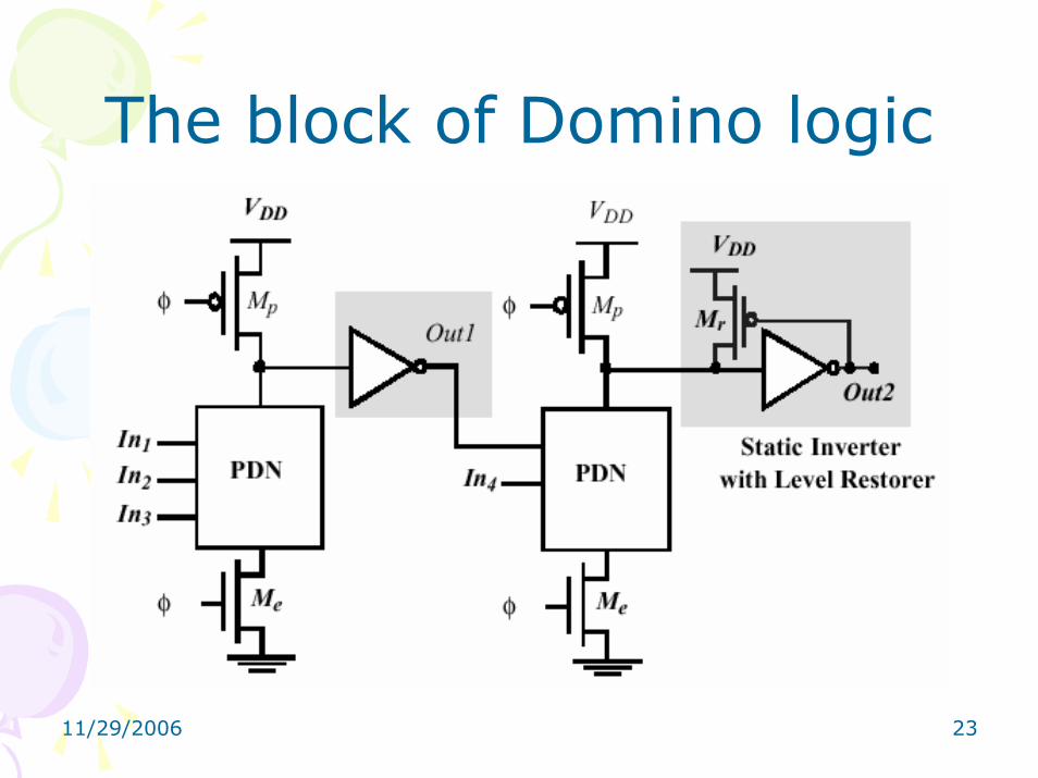
Domino logic Domino logic A Domino logic module consists of a φn
block followed by a static inverter. This ensures that all inputs to the next logic block are set to 0 after the precharge periods. Hence, the only possible transition during the evaluation period is 0 to 1 transition, so that formulated rule is obeyed.
11/29/2006 23
The block of Domino logic

11/29/2006 24
One Bit full AdderOne Bit full Adder--DominoDomino

11/29/2006 25
Simulation ResultsSimulation Results

11/29/2006 26
2-Phase Logic • We can use two-phase clock to
control logic transition similar to PE. A single clock (phi1 or phi2) is used to precharge and evaluate the logic block. The succeeding stage is operated on the opposite clock phase. A latch is needed between two stages.

11/29/2006 27
22--Phase logicPhase logic
ф1n-logic
ф2n-logic
Ф1’
ф1
ф1’
Ф1’
Ф2’
ф2
Ф2’
Ф2’
To ф1 stageFrom ф2 stage

11/29/2006 28
22--Phase Domino logicPhase Domino logic

11/29/2006 29
Multiple O/P Domino Logic
The main concept behind MODL is the utilization of subfunctions available in the logic tree of domino gates, thus saving replication of circuitry. The additional ouputs are obtained by adding precharge devices and static inverters at the corresponding intermediate nodes of the logic tree.

11/29/2006 30
Multiple output DominoMultiple output Domino

11/29/2006 31
MODL 4MODL 4--bit Carry Blockbit Carry Block
C 1 = G 1 + P 1 C 0 C 2 = G 2 + P 2 G 1 + P 2 P 1 C o
C 3 = G 3 + P 3 G 2 + P 3 P 2 G 1 +P 3 P 2 P 1 C 0 C 4 = G 4 + P 4 G 3 + P 4 P 3 G 2 +P 4 P 3 P 2 G 1 + P 4 P 3 P 2 P 1 C 0

11/29/2006 32
NORA Logic
• Combining C2MOS pipeline register and P-E CMOS dynamic logic function block, we get NORA-CMOS (mean NO-Race). The method is suitable for the implementation of pipelined datapaths.

11/29/2006 33
The block of NORA logic

11/29/2006 34
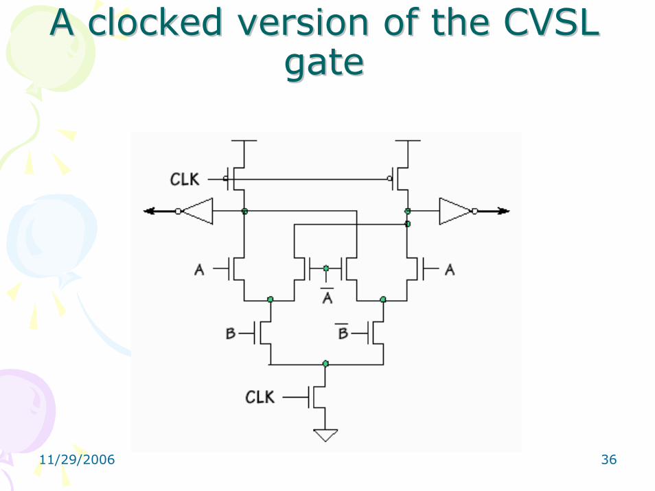
Cascode Logic• Further refinement leads to a clocked
version of the CVSL gate. This is really just two “Domino” gates operating on the true and complement inputs with a minimized logic tree. The advantage of this style of logic over domino logic is the ability to generate any logic expression, making it a complete logic family. This is achieved at the expense of the extra routing, active area, and complexity associated with dealing-rail logic.

11/29/2006 35
CASCOD LogicCASCOD Logic
11/29/2006 36
A clocked version of the CVSL A clocked version of the CVSL gategate

11/29/2006 37
The block of 8-bit DRCA using the Cascode logic
11/29/2006 38
Comparison of 8-bit Adders Designed with Dynamic Logic
Seven circuits using six dynamic logic functions are designed and simulated. The performance in terms of power, area, delay, energy and AT2 are compared.

11/29/2006 39
Dynamic Logic Adders that are designed and compared
• Domino logic 8-bit Adder• P-E logic 8-bit Adder • NORA logic 8-bit Adder • 2-Phase Logic 8-bit Adder • Multiple O/P Domino Logic 8-bit Adder • Cascode Logic 8-bit Adder

11/29/2006 40
Power

11/29/2006 41
Area

11/29/2006 42
DelayDelay

11/29/2006 43
DP

11/29/2006 44
AT2

11/29/2006 45
Conclusion
• Domino Logic: It has minimum area and number of transistors. The power consumption is low, and the delay is the longest. The DP and AT2 are average. If the design goal is minimum area and speed is a secondary concern the Domino logic is the best structure for Ripple Carry Adder.

11/29/2006 46
ConclusionConclusion……..
P-E Logic: has a small area and the minimum number of transistors. The power consumption is low, and the delay is short. It has the lower DP and AT2 for Ripple Carry Adder. If the logic has no inherent race problem, it will be the best choice for Ripple Carry Adder.

11/29/2006 47
ConclusionConclusion……..P-E (race-free) Logic: In order to avoid the
race condition of P-E Logic, the P-E (race-free) Logic is introduced. It has a small area and average of number of the transistors. The area and number of transistors is larger than P-E logic. The power consumption is average. The delay is shortest. It has lower DP and AT2 for Ripple Carry Adder. For synthesis, it is the best choice for Ripple Carry Adder.

11/29/2006 48
ConclusionConclusion……..•NORA Logic: The power consumption is higher. The area is small, and using a few transistors except Domino logic. The delay is longer. The DP is high and AT2 are average.

11/29/2006 49
ConclusionConclusion……..•2-Phase Logic: The area is larger and the number of transistors is more than others except Cascodelogic. The delay is longer. The power consumption, DP and AT2
are extremely high. Try to avoid this logic structure for designing Ripple Carry Adder.

11/29/2006 50
Ф1’ ф2’
ф1 ф2’
From ф2 To ф1 stages stage
Ф1’ ф2
Ф Ф1’ ф2’
Ф1block
Ф2 block

11/29/2006 51
2-phase domino logic
11/29/2006 52
Dynamic Circuits: Advantages & Dynamic Circuits: Advantages & DisadvantagesDisadvantages
Advantages:Circuits occupy less area the static circuitsOperate at higher speed than static CMOSNoise sensitive
Drawbacks:Affected by charge sharing and charge re-
distributionAlways require clocksCannot operate at low frequency Design is not straight forward