Embed Size (px)
Citation preview
PROJECT DUPLO
DUPLO Deliverable D2.2
Integration report of RF and antenna self-interference cancellation techniques Project Number: 316369
Project Title Full-Duplex Radios for Local Access – DUPLO
Deliverable Type: PU
Contractual Date of Delivery: October 31, 2014
Actual Date of Delivery: October 31, 2014
Editor(s): Björn Debaillie (IMEC)
Author(s): Cristina Lavín, Carmen Palacios (TTI); Björn Debaillie, Benjamin Hershberg, Barend van Liempd (IMEC);
Eric Klumperink, Dirk-Jan van den Broek (UT).
Work package: WP2
Estimated person months: 20
Security: PU
Nature: Report
Version: 1.0
Keyword list: full-duplex, design, antenna, RF circuits and systems, duplexer, self-interference, isolation, cancellation, polarized antenna, electrical balance, active cancellation
DUPLO WP2 D2.2 1 / 76
Ref. Ares(2015)1383010 - 30/03/2015
PROJECT DUPLO
Abstract: Full-duplex sets challenging requirements for wireless communication radios, in particular their capability to prevent receiver sensitivity degradation due to self-interference (transmit signals leaking into its own receiver). The DUPLO project mainly targets solutions for wireless radios to facilitate full-duplex operation in compact commercially attractive communication devices. This work package focusses on the design of small form-factor antenna structures and RF circuits which offer a substantial self-interference isolation or rejection and support integration with other solutions developed in the DUPLO project (e.g. baseband cancellation). Previously published techniques mainly rely on physical dimensions (i.e., antenna spacing) and/or require bulky components. Therefore, they are not applicable in the DUPLO project, as they hamper dense integration in compact radios.
The previous deliverables of this workpackage [1, 2] and the JSAC publication [3] report and motivate the architecture selection, design and initial measurements of the first antenna and RF prototype, and presents a theoretical link budget calculation methodology to derive the system component design requirements. Current document evaluates these earlier achieved results and develops, designs and fabricates new prototypes to improve the performance or to investigate the elimination of potential show-stoppers.
This document continues on the three designs presented in D2.1 [1, 3]. The first design covers a dual-polarized microstrip patch antenna, where a second prototype has been design and fabricated. This prototype offers improved bandwidth and has a smaller form factor compared to the first prototype. This second prototype has been designed based on parametric optimization and the measured performance has been reported. The second design covers a duplexer based on a tunable electrical balance circuit. Some severe limitations have been observed with the first electrical balance prototype in terms of bandwidth and linearity. To investigate if these limitations can be overcome, a second prototype has been designed and fabricated. This second prototype implements a highly linear balance network with multiple degrees of freedom to create multiple tunable isolation notches. The third design covers an active cancellation network operating on RF signals, capable of cancelling dynamically the self-interference. The performance of different cancellation networks, including components with variable gain, phase and time delay, with gain, are evaluated in combination with the antenna solution developed in this project.
These designs have been well received by the scientific community as this work has been accepted for publication in several peer-reviewed IEEE conferences. Compared to state-of-the-art, the developed designs differ mainly in terms of form-factor and integration potential in compact or portable radio system devices.
Disclaimer: This document reflects the contribution of the participants of the research project DUPLO. The European Union and its agencies are not liable or otherwise responsible for the contents of this document; its content reflects the view of its authors only. This document is provided without any warranty and does not constitute any commitment by any participant as to its content, and specifically excludes any warranty of correctness or fitness for a particular purpose. The user will use this document at the user's sole risk.
DUPLO WP2 D2.2 2 / 76
PROJECT DUPLO
Executive Summary This DUPLO WP2 deliverable D2.2 entitled “Integration report of RF and antenna self-interference cancellation techniques“ presents the second and final phase of the design and implementation of the prosed antenna and RF circuit solutions, enabling compact full-duplex wireless radio devices. This document evaluates the results achieved during the first phase, which are reported in D2.1 [1] and in the JSAC publication [3] and develops, designs and fabricates new prototypes to improve the performance or to investigate the elimination of potential show-stoppers.
The key design requirements in both phases are to minimize the RF self-interference and to target small form-factor antenna/RF solutions which can be implementable in compact radio devices. These requirements are however contradictory as dense integration and compact form-factor designs reduce the physical spacing between the transmitting and receiving elements/circuits/signals. In state-of-the-art full-duplex radio system design, this physical spacing is generally exploited to increase the self-interference isolation.
The presented techniques focus on antenna and RF circuit techniques only, and in combination with transceiver and digital cancellation techniques, an overall self-inference rejection of about 100dB is targeted for a mid-end scenario as described in D1.1 [4]. Based on the link budget calculation over realistic scenarios presented in D2.3.1 [2] and [3], the RF self-interference isolation factor should exceed 45 to 50dB over a bandwidth of 10MHz.
This document continues on the three designs presented in D2.1 [1, 3] covering a dual-polarized microstrip patch antenna design, and a tunable electrical balance duplexer design and an active cancellation network design to be applied at RF. This document describes how the performance of the designs can be improved, and validates these improvements based on the fabrication and measurements of new prototypes.
• A second dual-polarized microstrip patch antenna prototype has been designed, fabricated and measured. This prototype builds on similar topology as the first prototype and offers the same functionalities, but provides better performance (e.g. bandwidth) and is smaller in size. A parametric optimization methodology has been applied to specify the design parameters of the second prototype. The second prototype is smaller (60x60x8mm) and offers wider bandwidth capabilities with an SI isolation of 49dB over 10MHz and 42dB over 80MHz. Over 10MHz, antenna gain is higher than 6.5dB and offers a 3dB beamwidth of more than 70 degrees with an antenna efficiency of more than 75%. The isolation characteristics and robustness can be improved together with the active cancellation described in this document. This antenna prototype is used for integration in the DUPLO proof-of-concept demonstrator.
• Measurements in the electrical balance duplexer (EBD) first prototype indicated two main issues potentially hampering the exploitation for full-duplex operation. These issues are the limited bandwidth and the limited linearity of the balance network. These issues are described in this document and a second prototype has been designed and fabricated to investigate the capability to resolve these specific issues. To avoid the complexity overhead, this second prototype includes a tunable balance network only, without the transformer. This second prototype is implemented in SOI technology to leverage the linearity, and an additional degrees of tunability has been implemented in the balance network to trade-off the average SI isolation with the isolation bandwidth. The second prototype has been implemented in 0.18um SOI CMOS technology and covers an area of 0.9mm2 only. This design offers an extremely high linearity (IIP3 > 70dBm) and can handle relatively high transmission power (e.g. 27dBm) without considerable heating-up.
• The work on the active cancellation, initiated in D2.1 [1] has been continued and extended. This document details the design and component selection of the cancellation network and presents an automatic tuning method to control and tune the network to its optimal configuration in an efficient way. The active cancellation method has been verified based on measurements in combination with the second dual-polarized antenna prototype described in this document. These measurements
DUPLO WP2 D2.2 3 / 76
PROJECT DUPLO
indicate an additional SI reduction of 15dB in addition to the isolation provided by the antenna solution. The active cancellation performance has been also analyzed including a variable time delay element in the cancellation network.. This work is further continued in WP5.
The presented work mainly differentiates with state-of-the-art in terms of form factor and integration potential in compact or portable radio system devices. In this document, the developed techniques are compared with state-of-the-art solutions which apply similar techniques or topologies. With respect to the antenna, the usage of a single radiating element with orthogonal polarizations is hardly described in literature for full-duplex application, although dual-polarized antennas are frequently used in many others wireless communication systems. These dual-polarized elements enable to create compact form-factor full-duplex antennas. Their main limitation in full-duplex scenarios, is the small robustness of their isolation performance when external objects are close to the antenna. To increase this robustness, we developed the active cancellation network. With respect to the duplexer, electrical balancing designs for full-duplex are hardly described in literature. In FDD applications, full-duplex are more frequency considered, but our design outperforms the performances presented in literature. The designs presented in this document are well received by the scientific community as this work has been accepted for publication in several peer-reviewed IEEE conferences as described in chapter 6, and the comparison with state-of-the-art is given in chapter 7.
The results from WP2 are shared with the other workpackages within the DUPLO project as described in chapter 5.
DUPLO WP2 D2.2 4 / 76

PROJECT DUPLO
Authors
Partner Name Email
TTI Norte, SL (TTI) Cristina Lavín [email protected]
Carmen Palacios [email protected]
Interuniversitair Micro-Electronica Centrum vzw (IMEC)
Björn Debaillie [email protected]
Benjamin Hershberg [email protected]
Barend van Liempd [email protected]
Universiteit Twente (UT) Eric Klumperink [email protected]
Dirk-Jan van den Broek [email protected]
DUPLO WP2 D2.2 5 / 76

PROJECT DUPLO
Table of Contents
1. INTRODUCTION ........................................................................................................................... 10
2. FULL-DUPLEX TECHNOLOGY AT ANTENNA-LEVEL ............................................................. 12
2.1. INTRODUCTION ON ANTENNA TECHNIQUES ............................................................................. 12 2.1.1. Overview of the proposed solution ................................................................................... 12 2.1.2. Evaluation of the first DUPLO antenna prototype .......................................................... 14
2.2. SECOND DUAL-POLARIZED ANTENNA PROTOTYPE .................................................................. 15 2.2.1. Dual-polarized antenna design details ............................................................................. 15 2.2.1. Second prototype implementation and evaluation ......................................................... 21 2.2.2. Performance evaluation of the second antenna prototype ........................................... 26
3. FULL-DUPLEX TECHNOLOGY AT RF CIRCUIT LEVEL .......................................................... 27
3.1. THE ELECTRICAL-BALANCE DUPLEXER CONCEPT AND TARGET SPECIFICATIONS .................... 27 3.1.1. Limitations of the first prototype ....................................................................................... 28 3.1.2. Automatic tuning .................................................................................................................. 30
3.2. SECOND PROTOTYPE: HIGHLY-LINEAR, HIGHER-DIMENSIONAL BALANCE NETWORK ................ 31 3.2.1. Technology considerations: SOI CMOS versus bulk CMOS ........................................ 31 3.2.2. Design considerations ......................................................................................................... 32 3.2.3. Measurement results ............................................................................................................ 42 3.2.4. Summary ................................................................................................................................ 46
4. ACTIVE CANCELLATION ............................................................................................................ 48
4.1. INTRODUCTION TO ACTIVE CANCELLATION CONCEPT .............................................................. 48 4.2. ACTIVE CANCELLATION NETWORK IMPLEMENTATION AND INTEGRATION ................................. 49
4.2.1. Circuitry design and implementation ................................................................................ 49 4.2.2. Auto-tuning ............................................................................................................................ 53 4.2.3. Integration in DUPLO demonstrator .................................................................................. 54
4.3. JOINT DUAL-POLARIZED ANTENNA AND ACTIVE CANCELLATION NETWORK VALIDATION .......... 56 4.4. ANALYSIS OF ACTIVE CANCELLATION LIMITATIONS ................................................................. 58
4.4.1. Impact of passive suppression on self-interference response .................................... 58 4.4.2. Active cancellation including variable delay line ............................................................ 62
5. INTEGRATION AND VALIDATION POTENTIAL ........................................................................ 64
6. DISSEMINATION .......................................................................................................................... 66
7. STATE-OF-THE-ART AND FUTURE OPPORTUNITIES ............................................................ 68
7.1. DUAL-PORT FD ANTENNA SYSTEMS ....................................................................................... 68 7.2. ELECTRICAL BALANCE DUPLEXER .......................................................................................... 70
8. SUMMARY AND CONCLUSIONS ............................................................................................... 73
9. REFERENCES .............................................................................................................................. 75
DUPLO WP2 D2.2 6 / 76

PROJECT DUPLO
Acronyms and Abbreviations
3D three dimensions
AC alternating current
ANT antenna
BW bandwidth
C capacitance
cm centimeters
BS base station
CMOS complementary metal oxide semiconductor
D deliverable
DC direct current
DAC digital to analog converter
dB decibel
dBm power in decibels referenced to one milli-watt
DUPLO full-duplex radios for local access project
DUT device under test
EB electrical balance
EBD electrical balance duplexer
EMX electromagnetic simulator
EVM error vector magnitude FD full-duplex FDD frequency division duplex
FET field effect transistor
FFT fast Fourier transform
GHz giga (109) Herz
GND ground
HR high resistive
IBFD in-band full-duplex
IBM international business machines corporation.
IC integrated circuit
IEEE institute of Electrical and Electronics Engineers
I/O input/output
ISOL Isolation
IIP3 third-order interception point
IM intermodulation IM1 first order intermodulation product IM3 third order intermodulation product ISM industrial, scientific and medical LNA low noise amplifier
DUPLO WP2 D2.2 7 / 76
PROJECT DUPLO LO local oscillator LSB least significant bit
LTE long term evolution mA milli Ampere MHz mega (106) Hertz MIMO multiple input multiple output Mm millimeter MOS metal oxide semiconductor MSB most significant bit mS milli Siemens nH nano Henry NoC network on chip ns nano seconds OFDM orthogonal frequency-division multiplexing PA power amplifier PC personal computer PCB printed circuit board
pF pico Farad
PIFA planar Inverted-F Antenna PTx transmit power Q quality R resistor RF radio frequency RX receiver S.A. spectrum analyzer SAW surface acoustic wave SDR software defined radio SI self-interference SIC self-interference cancellation SMA sub-miniature version A SNDR signal to noise and distortion ratio SNR signal to noise ratio SoC system on chip
SOI silicon on insulator
SOTA state of the art STS short-training-sequence SV small variation TDD time division duplex TX transmitter u micro USB universal serial bus VGA variable gain control VSWR voltage standing wave ratio
DUPLO WP2 D2.2 8 / 76

PROJECT DUPLO W watt WARP wireless open-access research
WiFi WLAN products that are based on the Institute of Electrical and Electronics Engineers (IEEE) 802.11 standards
WLAN wireless local area network WP work package Zant antenna impedance Zbal balance network impedance
DUPLO WP2 D2.2 9 / 76
PROJECT DUPLO
1. INTRODUCTION
The DUPLO project aims to increase the spectral efficiency of wireless communication devices by investigating the full-duplex concept. This concept proposes concurrent transmission and reception on the same spectral resources, and thus theoretically doubling the spectral efficiency or enable new communication schemes as described in [4]. In practice, however, the benefits of full-duplex deployment rely on the availability of radio devices which support full-duplex operation. These radios are confronted with severe design challenges, namely:
• Isolation: to prevent the RF-signal generated by the local transmitter (TX) from leaking onto its own receiver (RX), where it causes self-interference.
• Cancellation: to subtract any remaining self-interference from the RX path using knowledge of the TX signal.
The DUPLO project identified and quantified the main design requirements over the targeted network types and scenarios , and gives a preliminary distribution of the technical requirements over the different building blocks [4]. For the WP2 activities, radio solutions are targeted which are commercially attractive in terms of form-factor, system integration, process technology and operation flexibility [3]. This target is different from the full-duplex radio solutions presented in literature which mainly rely on physical dimensions (i.e., antenna spacing) and require bulky components, hampering dense and cost-efficient integration. The WP2 objective is, however, contradicting with the self-interference problem which is easier to resolve with large form factor devices, circuits and antenna structures.
WP2 developed different techniques and prototype designs at the antenna, RF circuitry and transceiver level. Having self-interference isolation and cancellation at these levels is beneficial as it reduces the requirements on the transmitter dynamic range since all transmitter imperfections are included in the cancellation, and it reduces the requirements on the receiver dynamic range since the signal-to-interferer ratio is improved already before the LNA as discussed in [3]. The first results have been reported in the project deliverables D2.1 [1] and D2.3.1 [2], and have been published in JSAC [3]. These documents present a link budget calculation over realistic systems and scenarios, and report on the different design considerations, implementation topologies and initial measurements. Basically, D2.1 [1] describes three prototype designs which have been fabricated and measured:
• The antenna prototype, which is implemented as a dual-polarized microstrip patch antenna. The radiation polarization between transmission and reception is orthogonal to achieve an intrinsic isolation. D2.1 [1] describes the design considerations and optimizations, and illustrates both the simulated and measured antenna performance. The self-interference isolation robustness is also illustrated with objects in the direct surrounding of the antenna. More detailed results have been published in [5].
• The RF circuit transceiver, which acts as a duplexer and thus interconnects the RF transmitter and receiver ports with a single port antenna. This duplexer is implemented as an electrical balance circuit processed in plain CMOS technology. The functional circuit elements are an on-chip transformer, a tunable balance network and a basic LNA. The tunability of the balance network enables to match the antenna impedance over different operation conditions. D2.1 [1] describes the design considerations and optimizations, and illustrates the isolation, tuning capabilities, bandwidth and other relevant performance measures of the electrical balance duplexer. More detailed results have been published in [5].
• The active cancellation network, which connects the transmitter with the receiver path in the RF domain as close as possible to the dual-port antenna. This cancellation enables to add a modified copy of the transmitted signal to the receiver, thus enabling to cancel transmitted signals directly coupled to the receiver or to cancel the reflected signals due to near-field reflections. D2.1 [1]
DUPLO WP2 D2.2 10 / 76
PROJECT DUPLO
describes the selected topology, design considerations and initial performance measurements in combination with the antenna prototype also presented in D2.1 [1].
The work presented in D2.3.1 [2] and the progress of the analog transceiver design is not described in this document; it will be captured in the future WP2 deliverable D2.3.2. However, the main design requirement to provide an isolation of minimally 50dB over 10MHz in the direct path and eventually to provide an additional self-interference rejection circuit to suppress the near-field reflections is considered for the designs described in this document.
This document reports the final results on the antenna and RF circuitry work performed within WP2, by continuing the results presented in D2.1 [1]. With respect to prototype design, the following activities will be described:
• A second antenna prototype has been designed, fabricated and measured. This prototype builds on similar topology as the first prototype and offers the same functionalities, but provides better performance (e.g. bandwidth) and is smaller in size. A parametric optimization methodology has been applied to set the design parameters of this second antenna prototype. The measurement results of the second prototype are reported in this document. This second prototype will be used for integration in the WP5 activities, and the measurements are shared with WP3 to validate the digital cancellation algorithms.
• Measurements in the first electrical balance duplexer (EBD) prototype indicated two main issues potentially hampering the exploitation for full-duplex operation. These issues are the limited bandwidth and the limited linearity of the balance network. These issues are described in this document and a second prototype has been designed and fabricated to investigate the capability to resolve these specific issues. To avoid the complexity overhead, this second prototype includes the balance network only, without the transformer. Therefore, this prototype does not have the duplexer functionality and cannot be used in WP5. The first EBD prototype will be used for integration in WP5. Extensive measurements on the first prototype by using the prototype platform described in [6] are shared with WP3 to validate the digital cancellation algorithms.
• The work on the active cancellation has been continued by optimizing the network topology. The performance of the active cancellation network has been verified in combination with the antenna prototype, as reported in this document. This combination will be used for integration in WP5.
Given the growth of interest in full-duplex and the increased number of publications proposing new radio techniques, this document also gives an overview of current state-of-the-art which apply similar antenna or circuit topologies. The WP2 work has been published on top-tier and well-selected conferences and journals; the main accepted publications up to now are listed in chapter 6.
DUPLO WP2 D2.2 11 / 76
PROJECT DUPLO
2. FULL-DUPLEX TECHNOLOGY AT ANTENNA-LEVEL
2.1. Introduction on antenna techniques At antenna level, the DUPLO project focuses on the research of new antenna SI suppression techniques implementable in compact form-factor devices, which means that traditional antenna separation techniques thoroughly studied in literature ([7, 8, 9, 10, 11]) must be replaced by other antenna structures which allow efficient integration.
This document reports the optimization process of the full-duplex antenna solution which is described in detail in the previous deliverable D2.1 [1]. The design of the second antenna prototype is extensively described as well as its manufacturing and evaluation.
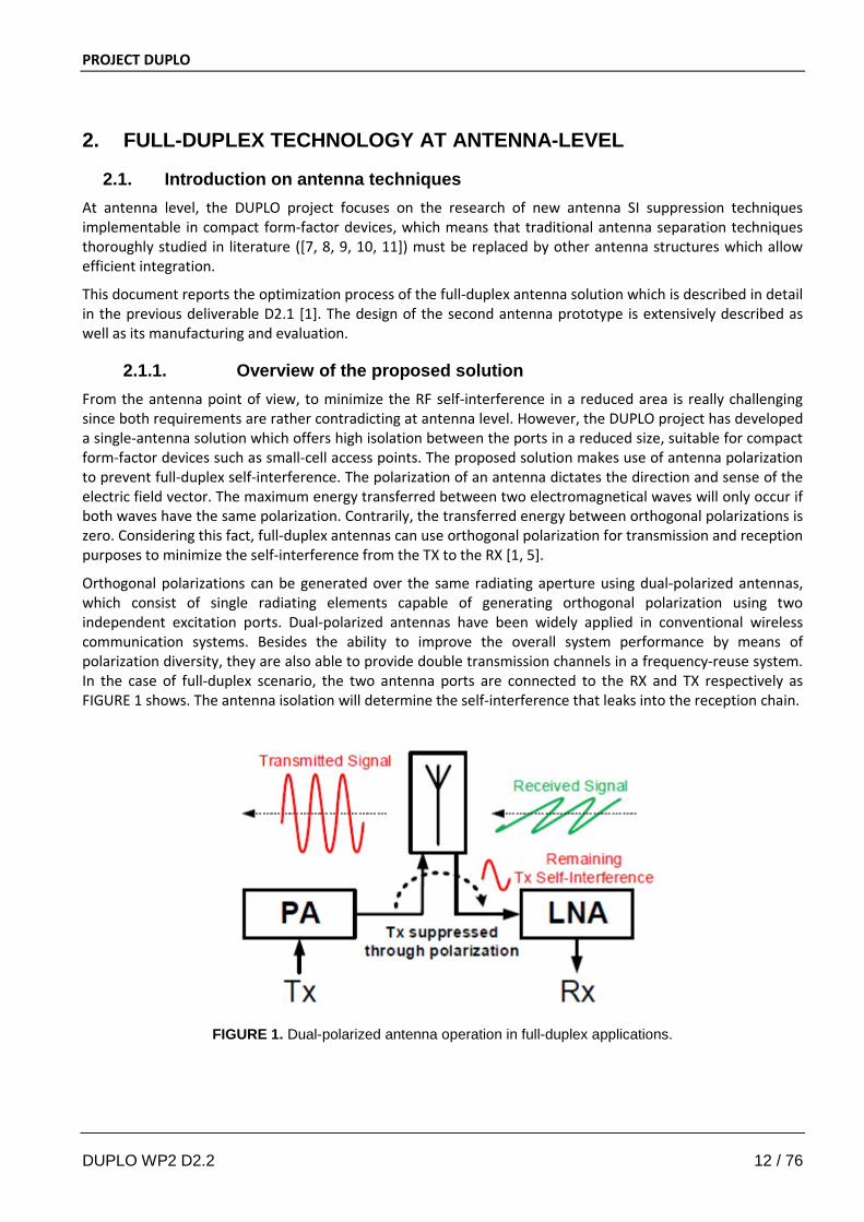
2.1.1. Overview of the proposed solution From the antenna point of view, to minimize the RF self-interference in a reduced area is really challenging since both requirements are rather contradicting at antenna level. However, the DUPLO project has developed a single-antenna solution which offers high isolation between the ports in a reduced size, suitable for compact form-factor devices such as small-cell access points. The proposed solution makes use of antenna polarization to prevent full-duplex self-interference. The polarization of an antenna dictates the direction and sense of the electric field vector. The maximum energy transferred between two electromagnetical waves will only occur if both waves have the same polarization. Contrarily, the transferred energy between orthogonal polarizations is zero. Considering this fact, full-duplex antennas can use orthogonal polarization for transmission and reception purposes to minimize the self-interference from the TX to the RX [1, 5].
Orthogonal polarizations can be generated over the same radiating aperture using dual-polarized antennas, which consist of single radiating elements capable of generating orthogonal polarization using two independent excitation ports. Dual-polarized antennas have been widely applied in conventional wireless communication systems. Besides the ability to improve the overall system performance by means of polarization diversity, they are also able to provide double transmission channels in a frequency-reuse system. In the case of full-duplex scenario, the two antenna ports are connected to the RX and TX respectively as FIGURE 1 shows. The antenna isolation will determine the self-interference that leaks into the reception chain.
FIGURE 1. Dual-polarized antenna operation in full-duplex applications.
DUPLO WP2 D2.2 12 / 76
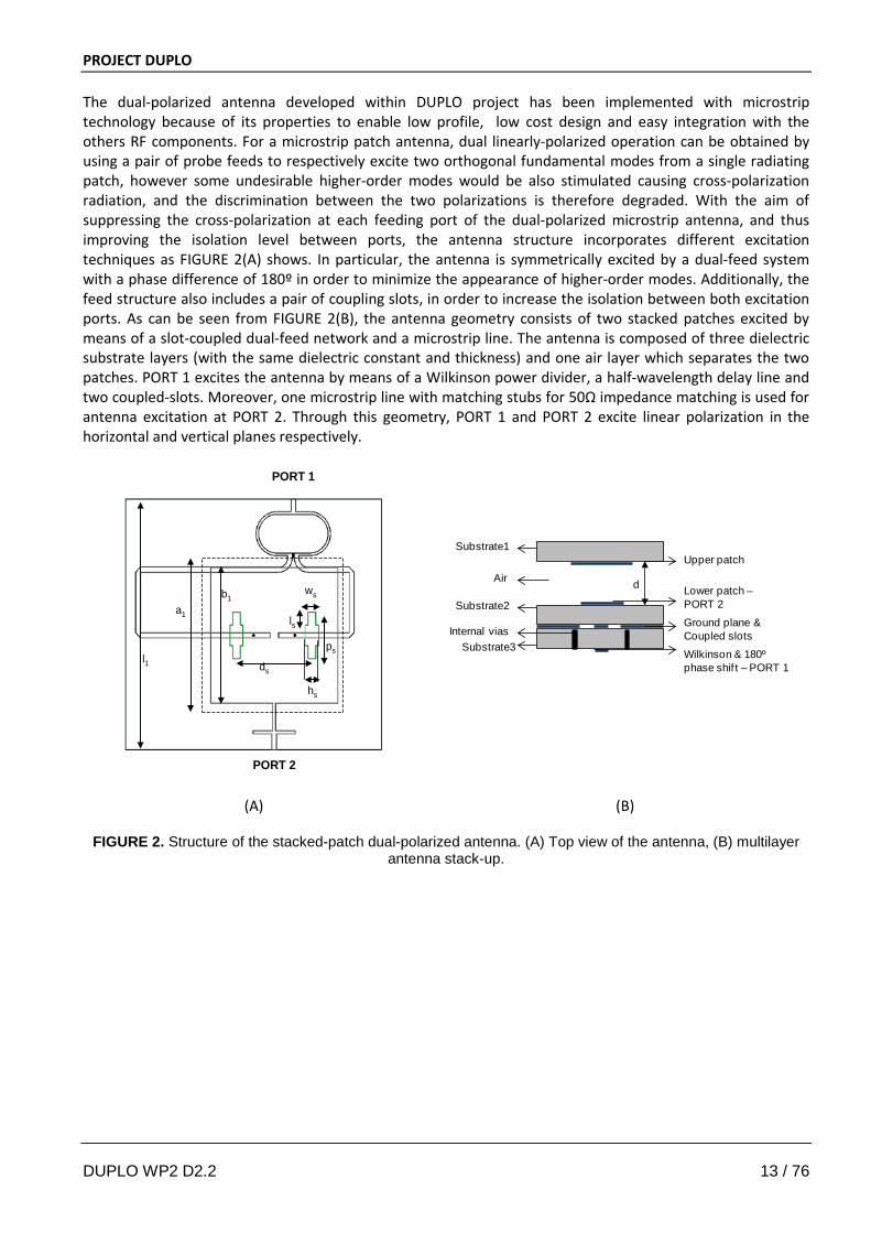
PROJECT DUPLO The dual-polarized antenna developed within DUPLO project has been implemented with microstrip technology because of its properties to enable low profile, low cost design and easy integration with the others RF components. For a microstrip patch antenna, dual linearly-polarized operation can be obtained by using a pair of probe feeds to respectively excite two orthogonal fundamental modes from a single radiating patch, however some undesirable higher-order modes would be also stimulated causing cross-polarization radiation, and the discrimination between the two polarizations is therefore degraded. With the aim of suppressing the cross-polarization at each feeding port of the dual-polarized microstrip antenna, and thus improving the isolation level between ports, the antenna structure incorporates different excitation techniques as FIGURE 2(A) shows. In particular, the antenna is symmetrically excited by a dual-feed system with a phase difference of 180º in order to minimize the appearance of higher-order modes. Additionally, the feed structure also includes a pair of coupling slots, in order to increase the isolation between both excitation ports. As can be seen from FIGURE 2(B), the antenna geometry consists of two stacked patches excited by means of a slot-coupled dual-feed network and a microstrip line. The antenna is composed of three dielectric substrate layers (with the same dielectric constant and thickness) and one air layer which separates the two patches. PORT 1 excites the antenna by means of a Wilkinson power divider, a half-wavelength delay line and two coupled-slots. Moreover, one microstrip line with matching stubs for 50Ω impedance matching is used for antenna excitation at PORT 2. Through this geometry, PORT 1 and PORT 2 excite linear polarization in the horizontal and vertical planes respectively.
PORT 1
PORT 2
a1
b1
ds
ls
ws
hs
psl1
Substrate1Upper patch
AirLower patch –PORT 2Substrate2Ground plane & Coupled slots
Substrate3Wilkinson & 180º phase shif t – PORT 1
Internal vias
d
(A) (B)
FIGURE 2. Structure of the stacked-patch dual-polarized antenna. (A) Top view of the antenna, (B) multilayer antenna stack-up.
DUPLO WP2 D2.2 13 / 76
PROJECT DUPLO
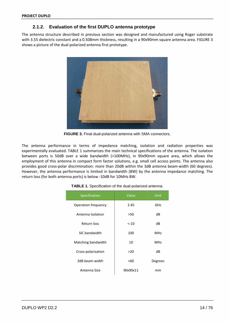
2.1.2. Evaluation of the first DUPLO antenna prototype The antenna structure described in previous section was designed and manufactured using Roger substrate with 3.55 dielectric constant and a 0.508mm thickness, resulting in a 90x90mm square antenna area. FIGURE 3 shows a picture of the dual-polarized antenna first prototype.
FIGURE 3. Final dual-polarized antenna with SMA connectors.
The antenna performance in terms of impedance matching, isolation and radiation properties was experimentally evaluated. TABLE 1 summarizes the main technical specifications of the antenna. The isolation between ports is 50dB over a wide bandwidth (>100MHz), in 90x90mm square area, which allows the employment of this antenna in compact form factor solutions, e.g. small cell access points. The antenna also provides good cross-polar discrimination: more than 20dB within the 3dB antenna beam-width (60 degrees). However, the antenna performance is limited in bandwidth (BW) by the antenna impedance matching. The return loss (for both antenna ports) is below -10dB for 10MHz BW.
TABLE 1. Specification of the dual-polarized antenna.
Specification Value Unit
Operation frequency 2.45 GHz
Antenna Isolation >50 dB
Return loss <-10 dB
SIC bandwidth 100 MHz
Matching bandwidth 10 MHz
Cross-polarization >20 dB
3dB beam-width >60 Degrees
Antenna Size 90x90x11 mm
DUPLO WP2 D2.2 14 / 76
PROJECT DUPLO The DUPLO project has selected 2.45GHz as the central frequency and a signal bandwidth of 10MHz for demonstration [12]. Therefore, this dual-polarized antenna prototype fully satisfies the technical requirements for the DUPLO proof-of-concept and is suitable for the integrated demonstrator. However, the reduced operational bandwidth (limited by the impedance matching) limits the capacity of the full-duplex link. This bandwidth limitation opens the door for antenna improvement with the aim of making it compatible with currently used wireless standards, e.g. WiFi standard from 2.4GHz to 2.48GHz. Consequently, based on the optimization of the results obtained from first antenna prototype introduced in deliverable D2.1, a second antenna prototype has been designed. The optimization process focused on the increment of the antenna bandwidth while maintaining the current performance in terms of antenna isolation. Additionally, the reduction of the antenna size was also objected during this optimization. The antenna structure proposed in D2.1 has been optimized and new excitation topologies have been explored to achieve the new technical requirements depicted in TABLE 2.
TABLE 2. Technical targets for dual-polarized antenna optimization.
Specification Value
Operation frequency WiFi band 2.4-2.48 GHz
Antenna Isolation >50
Return loss <-10
Cross-polarization >20
3dB beam-width >60
Antenna size Reduction of radiating area in more than 30%
2.2. Second dual-polarized antenna prototype
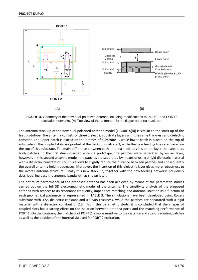
2.2.1. Dual-polarized antenna design details As mentioned in previous section, the structure of the dual-polarized antenna first prototype has been modified in order to reach more challenging requirements. The DUPLO project mainly targets solutions for wireless radios to make possible full-duplex operation in compact form factor devices, therefore the reduction of the size of the developed solutions is crucial. Considering the antenna geometry showed in FIGURE 2, the dual-polarized antenna size is mainly limited by the excitation networks used for the generation of highly-isolated dual-orthogonal polarizations. To overcome this size limitation, the feeding networks of both ports have been replaced by more compact solutions. Firstly, PORT 1 is excited by 180º phase shifted lines combined by a Wilkinson divider which use a lot of space on the bottom of the substrate 3. This feeding network has been replaced by a 1:2 divider and a meander line which introduces 180º phase shift between the divider branches, as FIGURE 4 illustrates. By doing so, the signals have equal amplitudes and 180º phase difference when they arrive to the coupled-slots. Consequently, the x-directed polarization mode is symmetrically excited through PORT 1, and the higher-order modes are suppressed. Secondly, in the first dual-polarized antenna model, PORT 2 is excited by a microstrip line including 50Ω matching stubs, imposing to lengthen the size of the overall antenna along the y-axis. However, the use of an internal via would provide some extra area to host the microstrip line, while the position of this internal via with respect to the excitation patch can be used to tune the 50Ω matching of PORT 2. By doing so, the size of the dual-polarized antenna can be reduced by 30%, resulting in an overall dimension of 60x60mm. The new dual-polarized antenna geometry is given in FIGURE 4(A) where both new feeding networks for respectively PORT1 and PORT2 are shown.
DUPLO WP2 D2.2 15 / 76
PROJECT DUPLO
PORT 1
PORT 2
a1
b1
ds
ws
ls
ps
pv
hs
x
y
l1
Substrate1Upper patch
Lower PatchSubstrate2
Gound plane & Coupled slots
PORT2 PORT1 (Divider & 180º phase shif t)
DielectricMaterial d
Substrate3
(A) (B)
FIGURE 4. Geometry of the new dual-polarized antenna including modifications to PORT1 and PORT2 excitation networks. (A) Top view of the antenna, (B) multilayer antenna stack-up.
The antenna stack-up of the new dual-polarized antenna model (FIGURE 4(B)) is similar to the stack-up of the first prototype. The antenna consists of three dielectric substrate layers with the same thickness and dielectric constant. The upper patch is placed on the bottom of substrate 1, while lower patch is placed on the top of substrate 2. The coupled slots are printed of the back of substrate 3, while the new feeding lines are placed on the top of this substrate. The main difference between both antenna stack-ups lies on the layer that separates both patches. In the first dual-polarized antenna prototype, the patches were separated by an air layer, however, in this second antenna model, the patches are separated by means of using a rigid dielectric material with a dielectric constant of 2.5. This allows to slightly reduce the distance between patches and consequently the overall antenna height decreases. Moreover, the insertion of this dielectric layer gives more robustness to the overall antenna structure. Finally this new stack-up, together with the new feeding networks previously described, increase the antenna bandwidth as shown later.
The optimum performance of the proposed antenna has been achieved by means of the parametric studies carried out on the full 3D electromagnetic model of the antenna. The sensitivity analysis of the proposed antenna with respect to its resonance frequency, impedance matching and antenna isolation as a function of each geometrical parameter is represented in TABLE 3. The simulations have been developed using Rogers substrate with 3.55 dielectric constant and a 0.508 thickness, while the patches are separated with a rigid material with a dielectric constant of 2.5. From this parametric study, it is concluded that the shapes of coupled slots has a strong effect on the isolation between antenna ports and the matching performance of PORT 1. On the contrary, the matching of PORT 2 is more sensitive to the distance and size of radiating patches as well as the position of the internal via used for PORT 2 excitation.
DUPLO WP2 D2.2 16 / 76
PROJECT DUPLO
TABLE 3. Parametric studies of the proposed antenna with respect to its resonance frequency, impedance matching and antenna isolation as a function of the design geometrical parameters. (SV - small variation)
Geometrical Parameter Resonance frequency
Impedance Matching Antenna Isolation
Length of upper patch (a1 ↑) ↓ ↓ SV
Length of lower patch (b1↑) ↓ ↓ SV
Distance between coupled slots (ds↑) PORT 1 -↓ PORT 2 - SV
PORT 1 -↓ PORT 2 - SV SV
Length of coupled slots (ps↑) PORT 1 -↑ PORT 2 - SV
PORT 1 - SV PORT 2 - SV ↓
Width of coupled slots (hs↑) PORT 1 -↑ PORT 2 - SV
PORT 1 - ↓ PORT 2 - SV ↓
Length of coupled slots- upper/lower part (ls↑) PORT 1 -↑ PORT 2 -SV
PORT 1 - ↑ PORT 2 - SV ↓
Width of upper part of coupled slots- upper/lower part (ws↑) PORT 1 - ↓ PORT 2 -SV
PORT 1 - SV PORT 2 - SV ↓
Position of the internal via - PORT2 (pv ↑) PORT 1 -SV PORT 2 - ↓
PORT 1 -SV PORT 2 - ↓ SV
Distance between patches (d↑) ↓ ↓ SV
The optimization of the geometrical antenna parameters has been carried out defining an input impedance matching better than -10dB and an isolation better that -50dB as target objectives. Additionally, the Trust Region Framework algorithm has been used for the parametrical optimization. This algorithm is a local optimizer which builds a linear model on primary data in a region around the starting point. Then, the modeled solution is used as new starting point until it converges to an accurate model of the data. In the case of the proposed new dual-polarized antenna structure, this algorithm takes the advantage of input impedance matching and antenna isolation sensitivity to reduce the number of simulations needed and thus speed up the process of optimization [13]. The optimum dimensions obtained from this parametrical optimization are depicted in TABLE 4.
DUPLO WP2 D2.2 17 / 76
PROJECT DUPLO
TABLE 4. Dual-polarized antenna design parameters.
Geometrical Antenna Parameter Value
d[mm] 6.97
l1[mm] 60.00
a1[mm] 33.07
b1[mm] 30.43
ds [mm] 20.34
ps [mm] 13.73
ls [mm] 3.96
hs [mm] 2.47
ws [mm] 3.16
pv [mm] 20.2
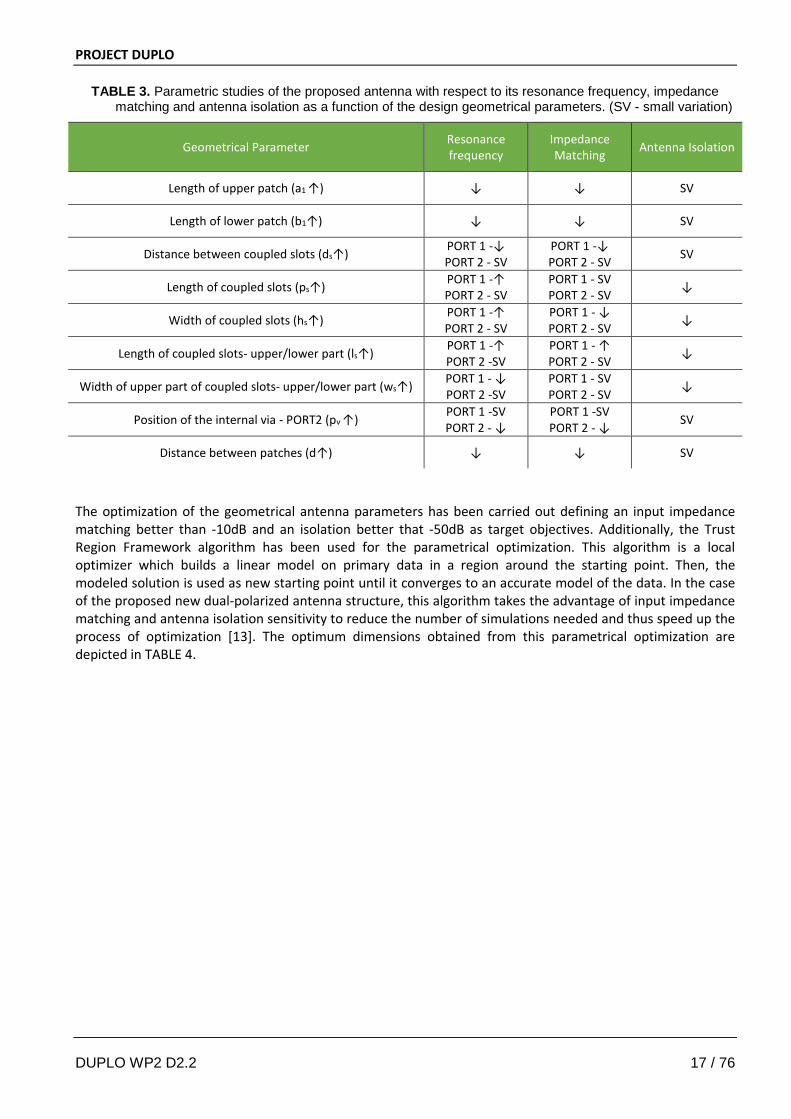
The simulation results considering these geometrical values are presented in FIGURE 5(A) and FIGURE 5(B) respectively. These simulation results show an isolation between ports better than50dB over the full antenna impedance bandwidth, while the antenna impedance is better than -10dB in more than 70MHz BW.
2.3 2.35 2.4 2.45 2.5 2.55 2.6-60
-50
-40
-30
-20
-10
0
Frequency (GHz)
Ret
urn
Loss
(dB
)
PORT 1PORT 2
2.3 2.35 2.4 2.45 2.5 2.55 2.6
-60
-50
-40
-30
-20
Frequency (GHz)
Isol
atio
n (d
B)
Isolation
(A) (B)
FIGURE 5. Simulated results for the optimized dual-polarized antenna. (A) Return Loss, (B) isolation between antenna ports.
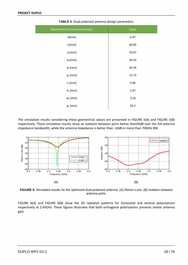
FIGURE 6(A) and FIGURE 6(B) show the 3D radiation patterns for horizontal and vertical polarizations respectively at 2.45GHz. These figures illustrates that both orthogonal polarizations presents similar antenna gain.
DUPLO WP2 D2.2 18 / 76
PROJECT DUPLO
(A) (B)
FIGURE 6. Simulated Radiation pattern results for the dual-polarized antenna at 2.45GHz. (A) Horizontal polarization, (B) vertical polarization.
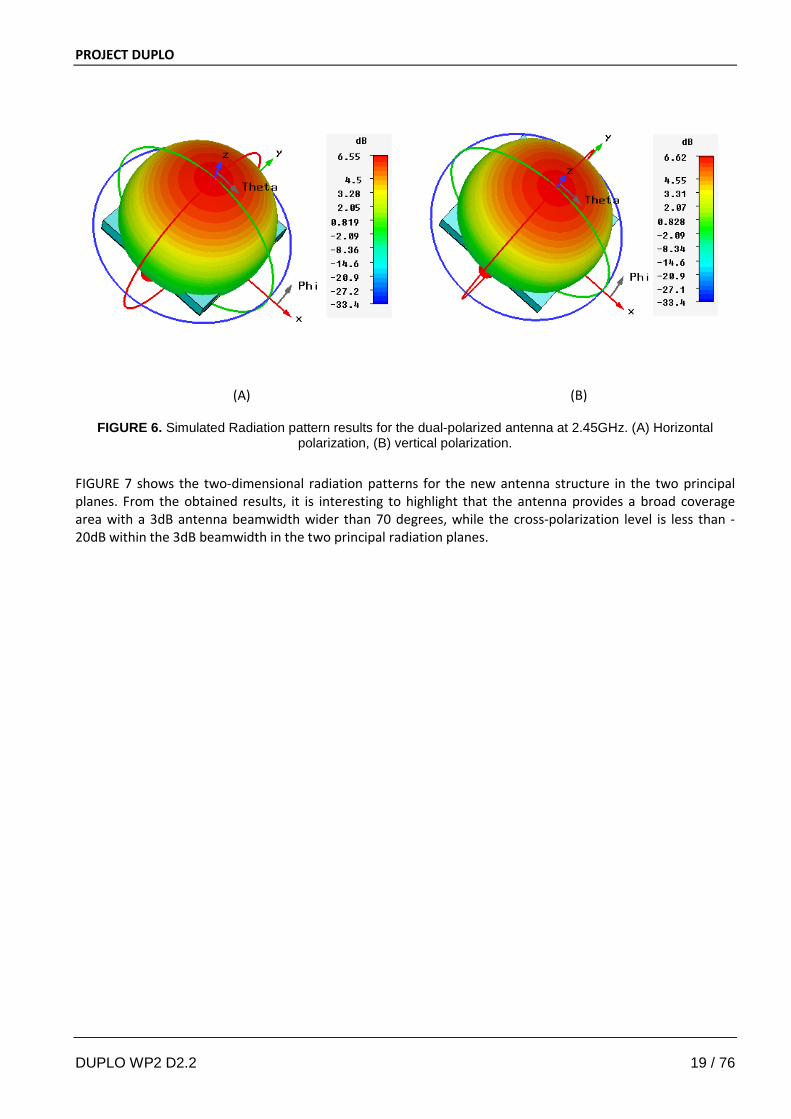
FIGURE 7 shows the two-dimensional radiation patterns for the new antenna structure in the two principal planes. From the obtained results, it is interesting to highlight that the antenna provides a broad coverage area with a 3dB antenna beamwidth wider than 70 degrees, while the cross-polarization level is less than -20dB within the 3dB beamwidth in the two principal radiation planes.
DUPLO WP2 D2.2 19 / 76
PROJECT DUPLO
(A) (B)
(C) (D)
FIGURE 7. Simulated co-polarization and cross-polarization radiation patterns at 2.45 GHz. (A) E-plane for PORT 1, (B) H-plane for PORT 1, (C) E-plane for PORT 2, (D) H-plane for PORT 2.
DUPLO WP2 D2.2 20 / 76
PROJECT DUPLO
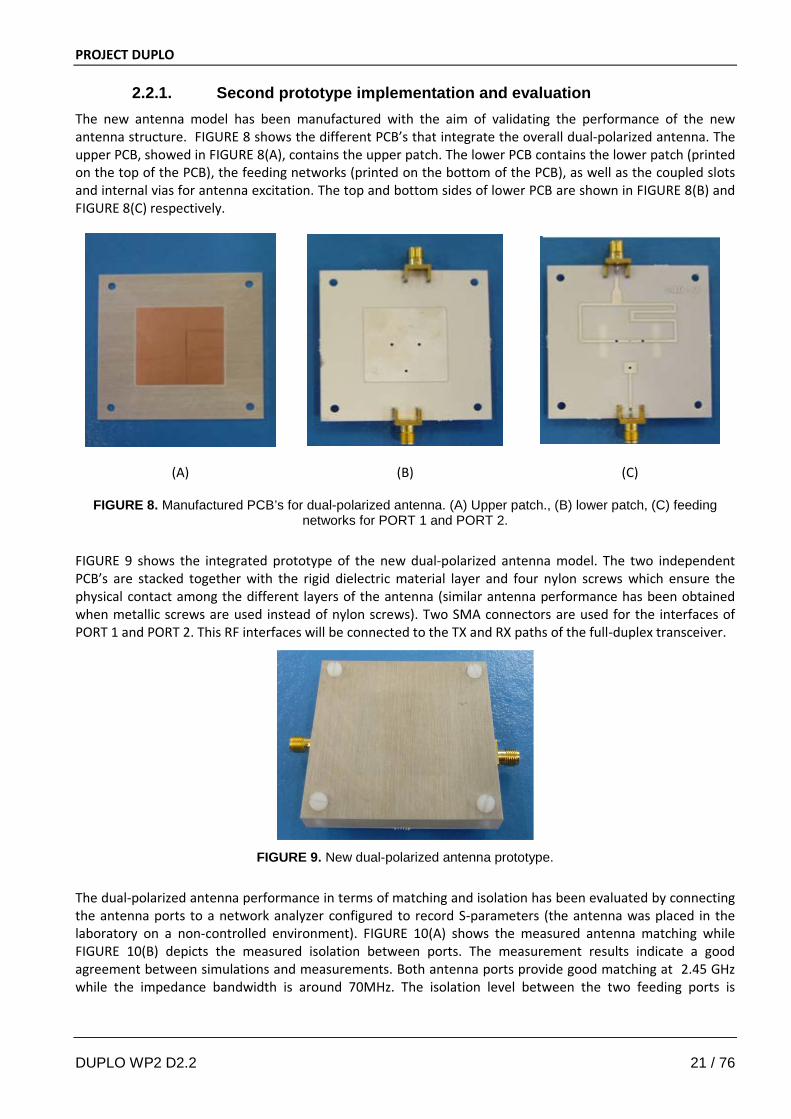
2.2.1. Second prototype implementation and evaluation The new antenna model has been manufactured with the aim of validating the performance of the new antenna structure. FIGURE 8 shows the different PCB’s that integrate the overall dual-polarized antenna. The upper PCB, showed in FIGURE 8(A), contains the upper patch. The lower PCB contains the lower patch (printed on the top of the PCB), the feeding networks (printed on the bottom of the PCB), as well as the coupled slots and internal vias for antenna excitation. The top and bottom sides of lower PCB are shown in FIGURE 8(B) and FIGURE 8(C) respectively.
(A) (B) (C)
FIGURE 8. Manufactured PCB’s for dual-polarized antenna. (A) Upper patch., (B) lower patch, (C) feeding networks for PORT 1 and PORT 2.
FIGURE 9 shows the integrated prototype of the new dual-polarized antenna model. The two independent PCB’s are stacked together with the rigid dielectric material layer and four nylon screws which ensure the physical contact among the different layers of the antenna (similar antenna performance has been obtained when metallic screws are used instead of nylon screws). Two SMA connectors are used for the interfaces of PORT 1 and PORT 2. This RF interfaces will be connected to the TX and RX paths of the full-duplex transceiver.
FIGURE 9. New dual-polarized antenna prototype.
The dual-polarized antenna performance in terms of matching and isolation has been evaluated by connecting the antenna ports to a network analyzer configured to record S-parameters (the antenna was placed in the laboratory on a non-controlled environment). FIGURE 10(A) shows the measured antenna matching while FIGURE 10(B) depicts the measured isolation between ports. The measurement results indicate a good agreement between simulations and measurements. Both antenna ports provide good matching at 2.45 GHz while the impedance bandwidth is around 70MHz. The isolation level between the two feeding ports is
DUPLO WP2 D2.2 21 / 76
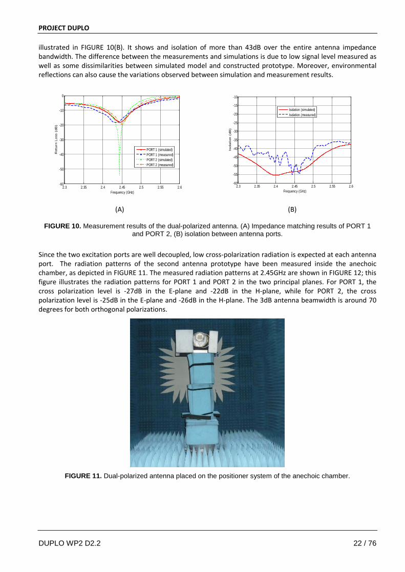
PROJECT DUPLO illustrated in FIGURE 10(B). It shows and isolation of more than 43dB over the entire antenna impedance bandwidth. The difference between the measurements and simulations is due to low signal level measured as well as some dissimilarities between simulated model and constructed prototype. Moreover, environmental reflections can also cause the variations observed between simulation and measurement results.
2.3 2.35 2.4 2.45 2.5 2.55 2.6-60
-50
-40
-30
-20
-10
0
Frequency (GHz)
Ret
urn
Lo
ss (
dB)
PORT 1 (simulated)PORT 1 (measured)PORT 2 (simulated)PORT 2 (measured)
2.3 2.35 2.4 2.45 2.5 2.55 2.6
-60
-55
-50
-45
-40
-35
-30
-25
-20
-15
-10
Frequency (GHz)
Isol
ati
on (
dB)
Isolation (simulated)Isolation (measured)
(A) (B)
FIGURE 10. Measurement results of the dual-polarized antenna. (A) Impedance matching results of PORT 1 and PORT 2, (B) isolation between antenna ports.
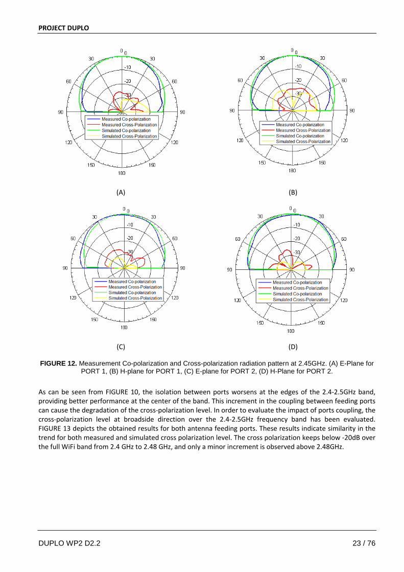
Since the two excitation ports are well decoupled, low cross-polarization radiation is expected at each antenna port. The radiation patterns of the second antenna prototype have been measured inside the anechoic chamber, as depicted in FIGURE 11. The measured radiation patterns at 2.45GHz are shown in FIGURE 12; this figure illustrates the radiation patterns for PORT 1 and PORT 2 in the two principal planes. For PORT 1, the cross polarization level is -27dB in the E-plane and -22dB in the H-plane, while for PORT 2, the cross polarization level is -25dB in the E-plane and -26dB in the H-plane. The 3dB antenna beamwidth is around 70 degrees for both orthogonal polarizations.
FIGURE 11. Dual-polarized antenna placed on the positioner system of the anechoic chamber.
DUPLO WP2 D2.2 22 / 76
PROJECT DUPLO
(A) (B)
(C) (D)
FIGURE 12. Measurement Co-polarization and Cross-polarization radiation pattern at 2.45GHz. (A) E-Plane for PORT 1, (B) H-plane for PORT 1, (C) E-plane for PORT 2, (D) H-Plane for PORT 2.
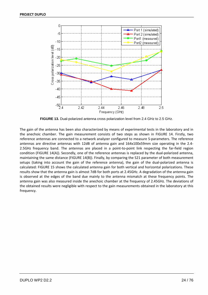
As can be seen from FIGURE 10, the isolation between ports worsens at the edges of the 2.4-2.5GHz band, providing better performance at the center of the band. This increment in the coupling between feeding ports can cause the degradation of the cross-polarization level. In order to evaluate the impact of ports coupling, the cross-polarization level at broadside direction over the 2.4-2.5GHz frequency band has been evaluated. FIGURE 13 depicts the obtained results for both antenna feeding ports. These results indicate similarity in the trend for both measured and simulated cross polarization level. The cross polarization keeps below -20dB over the full WiFi band from 2.4 GHz to 2.48 GHz, and only a minor increment is observed above 2.48GHz.
DUPLO WP2 D2.2 23 / 76
PROJECT DUPLO
FIGURE 13. Dual-polarized antenna cross polarization level from 2.4 GHz to 2.5 GHz.
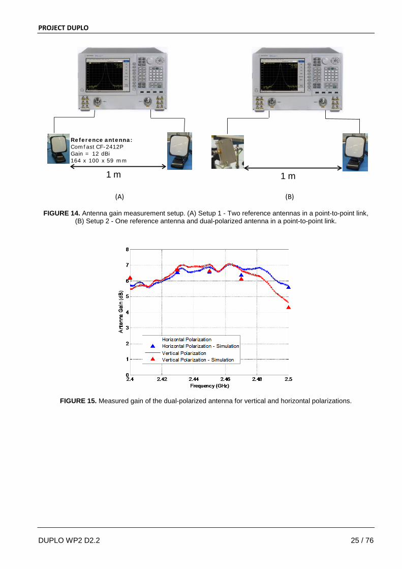
The gain of the antenna has been also characterized by means of experimental tests in the laboratory and in the anechoic chamber. The gain measurement consists of two steps as shown in FIGURE 14. Firstly, two reference antennas are connected to a network analyzer configured to measure S-parameters. The reference antennas are directive antennas with 12dB of antenna gain and 164x100x59mm size operating in the 2.4-2.5GHz frequency band. The antennas are placed in a point-to-point link respecting the far-field region condition (FIGURE 14(A)). Secondly, one of the reference antennas is replaced by the dual-polarized antenna, maintaining the same distance (FIGURE 14(B)). Finally, by comparing the S21 parameter of both measurement setups (taking into account the gain of the reference antenna), the gain of the dual-polarized antenna is calculated: FIGURE 15 shows the calculated antenna gain for both vertical and horizontal polarizations. These results show that the antenna gain is almost 7dB for both ports at 2.45GHz. A degradation of the antenna gain is observed at the edges of the band due mainly to the antenna mismatch at these frequency points. The antenna gain was also measured inside the anechoic chamber at the frequency of 2.45GHz. The deviations of the obtained results were negligible with respect to the gain measurements obtained in the laboratory at this frequency.
DUPLO WP2 D2.2 24 / 76
PROJECT DUPLO
1 m
Reference antenna:Comfast CF-2412PGain = 12 dBi164 x 100 x 59 mm
1 m
(A) (B)
FIGURE 14. Antenna gain measurement setup. (A) Setup 1 - Two reference antennas in a point-to-point link, (B) Setup 2 - One reference antenna and dual-polarized antenna in a point-to-point link.
FIGURE 15. Measured gain of the dual-polarized antenna for vertical and horizontal polarizations.
DUPLO WP2 D2.2 25 / 76
PROJECT DUPLO
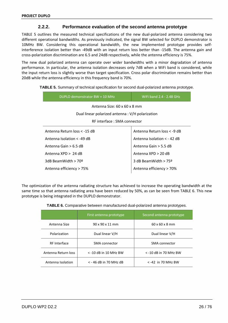
2.2.2. Performance evaluation of the second antenna prototype TABLE 5 outlines the measured technical specifications of the new dual-polarized antenna considering two different operational bandwidths. As previously indicated, the signal BW selected for DUPLO demonstrator is 10MHz BW. Considering this operational bandwidth, the new implemented prototype provides self-interference isolation better than -49dB with an input return loss better than -15dB. The antenna gain and cross-polarization discrimination are 6.5 and 24dB respectively, while the antenna efficiency is 75%.
The new dual polarized antenna can operate over wider bandwidths with a minor degradation of antenna performance. In particular, the antenna isolation decreases only 7dB when a WiFi band is considered, while the input return loss is slightly worse than target specification. Cross polar discrimination remains better than 20dB while the antenna efficiency in this frequency band is 70%.
TABLE 5. Summary of technical specification for second dual-polarized antenna prototype.
DUPLO demonstrator BW = 10 MHz WiFi band 2.4 - 2.48 GHz
Antenna Size: 60 x 60 x 8 mm
Dual linear polarized antenna : V/H polarization
RF interface : SMA connector
Antenna Return loss < -15 dB
Antenna Isolation < -49 dB
Antenna Gain > 6.5 dB
Antenna XPD > 24 dB
3dB BeamWidth > 70º
Antenna efficiency > 75%
Antenna Return loss < -9 dB
Antenna Isolation < - 42 dB
Antenna Gain > 5.5 dB
Antenna XPD > 20 dB
3 dB BeamWidth > 75º
Antenna efficiency > 70%
The optimization of the antenna radiating structure has achieved to increase the operating bandwidth at the same time so that antenna radiating area have been reduced by 50%, as can be seen from TABLE 6. This new prototype is being integrated in the DUPLO demonstrator.
TABLE 6. Comparative between manufactured dual-polarized antenna prototypes.
First antenna prototype Second antenna prototype
Antenna Size 90 x 90 x 11 mm 60 x 60 x 8 mm
Polarization Dual linear V/H Dual linear V/H
RF Interface SMA connector SMA connector
Antenna Return loss < -10 dB in 10 MHz BW < -10 dB in 70 MHz BW
Antenna Isolation < - 46 dB in 70 MHz dB < -42 in 70 MHz BW
DUPLO WP2 D2.2 26 / 76
PROJECT DUPLO
3. FULL-DUPLEX TECHNOLOGY AT RF CIRCUIT LEVEL
With the 180nm CMOS prototype [5] this work package managed to demonstrate the feasibility of using electrical balance duplexers to cancel self-interference at the direct RF interface between the antenna and the transceiver. In this chapter, we will briefly explain the operation of the EBD and discuss the target specifications. Then, a new prototype chip which was fabricated and tested in order to combat some of the remaining limitations of the first prototype is presented.
3.1. The electrical-balance duplexer concept and target specifications In full duplex operation, concurrent TX and RX operation at the same frequency is required. Recently, the use of hybrid transformers to achieve signal cancellation based on electrical balance (EB) has been proposed to achieve tunable duplexer filters for FDD [14, 15, 16]. In task 2.2, this technique is applied in the context of full duplex, where it shows to provide RF self-interference cancellation for compact radio devices [3, 5, 1].
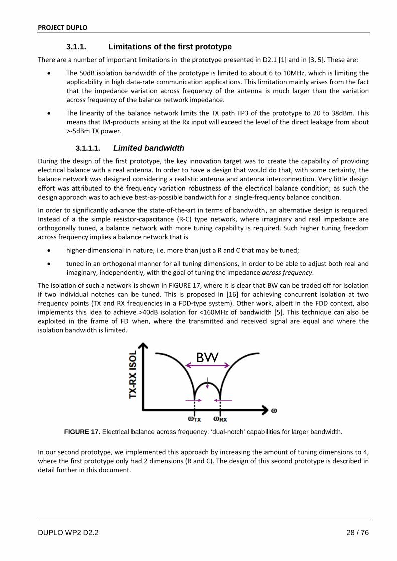
FIGURE 16 shows the conceptual operation of an EB duplexer, comprising a hybrid transformer and a so-called balance network, which is essentially a tunable dummy load impedance.
FIGURE 16. Electrical balance operating principle for (a) TX operation and (b) RX operation: in FD, (a) and (b)
occur at the same time and frequency.
Ideally, the transmitter signal (output of the PA) splits up exactly between the antenna and the balance network, so that no differential voltage excitation occurs and the hybrid transformer essentially subtracts the voltage across these impedances. This so-called “electrical balance condition” is limited by the accuracy with which the balance network impedance (ZBAL) can mimic antenna impedance (ZANT). By tuning the resistance and reactance of balance network independently with high precision, >50dB of self-interference cancelation (SIC) can be achieved across the channel bandwidth (BW) [14]. By virtue of this purely passive cancellation process, any noise and nonlinearity products generated in the transmitter are also cancelled in such electrical balance condition.
The principle of electrical balance is applicable to both FDD and FD: the TX to ZANT path as well as the ZANT to RX path have a wideband transformer response, while the TX to RX cancellation is required at both the TX and RX frequencies simultaneously (FDD) [15] or at a single frequency only (FD).
In our previous work [3], [1], we have proposed the usage of an EBD to enable self-interference cancellation in RF for FD operation, and its potential has been validated based on real measurements with on a prototype [5]. This prototype has been integrated in a test and validation radio platform, and an intelligent tuning algorithm has been developed. This work has been published [6] and is considered as part of the DUPLO WP5 activities.
DUPLO WP2 D2.2 27 / 76
PROJECT DUPLO
3.1.1. Limitations of the first prototype There are a number of important limitations in the prototype presented in D2.1 [1] and in [3, 5]. These are:
• The 50dB isolation bandwidth of the prototype is limited to about 6 to 10MHz, which is limiting the applicability in high data-rate communication applications. This limitation mainly arises from the fact that the impedance variation across frequency of the antenna is much larger than the variation across frequency of the balance network impedance.
• The linearity of the balance network limits the TX path IIP3 of the prototype to 20 to 38dBm. This means that IM-products arising at the Rx input will exceed the level of the direct leakage from about >-5dBm TX power.
3.1.1.1. Limited bandwidth During the design of the first prototype, the key innovation target was to create the capability of providing electrical balance with a real antenna. In order to have a design that would do that, with some certainty, the balance network was designed considering a realistic antenna and antenna interconnection. Very little design effort was attributed to the frequency variation robustness of the electrical balance condition; as such the design approach was to achieve best-as-possible bandwidth for a single-frequency balance condition.
In order to significantly advance the state-of-the-art in terms of bandwidth, an alternative design is required. Instead of a the simple resistor-capacitance (R-C) type network, where imaginary and real impedance are orthogonally tuned, a balance network with more tuning capability is required. Such higher tuning freedom across frequency implies a balance network that is
• higher-dimensional in nature, i.e. more than just a R and C that may be tuned;
• tuned in an orthogonal manner for all tuning dimensions, in order to be able to adjust both real and imaginary, independently, with the goal of tuning the impedance across frequency.
The isolation of such a network is shown in FIGURE 17, where it is clear that BW can be traded off for isolation if two individual notches can be tuned. This is proposed in [16] for achieving concurrent isolation at two frequency points (TX and RX frequencies in a FDD-type system). Other work, albeit in the FDD context, also implements this idea to achieve >40dB isolation for <160MHz of bandwidth [5]. This technique can also be exploited in the frame of FD when, where the transmitted and received signal are equal and where the isolation bandwidth is limited.
BW
FIGURE 17. Electrical balance across frequency: ‘dual-notch’ capabilities for larger bandwidth.
In our second prototype, we implemented this approach by increasing the amount of tuning dimensions to 4, where the first prototype only had 2 dimensions (R and C). The design of this second prototype is described in detail further in this document.
DUPLO WP2 D2.2 28 / 76
PROJECT DUPLO
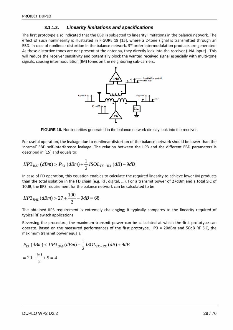
3.1.1.2. Linearity limitations and specifications The first prototype also indicated that the EBD is subjected to linearity limitations in the balance network. The effect of such nonlinearity is illustrated in FIGURE 18 [15], where a 2-tone signal is transmitted through an EBD. In case of nonlinear distortion in the balance network, 3rd order intermodulation products are generated. As these distortive tones are not present at the antenna, they directly leak into the receiver (LNA input) . This will reduce the receiver sensitivity and potentially block the wanted received signal especially with multi-tone signals, causing intermodulation (IM) tones on the neighboring sub-carriers.
FIGURE 18. Nonlinearities generated in the balance network directly leak into the receiver.
For useful operation, the leakage due to nonlinear distortion of the balance network should be lower than the ‘normal’ EBD self-interference leakage. The relation between the IIP3 and the different EBD parameters is described in [15] and equals to:
dBdBISOLdBmPdBmIIP RXTXTXBAL 9)(21)()(3 −+> −
In case of FD operation, this equation enables to calculate the required linearity to achieve lower IM products than the total isolation in the FD chain (e.g. RF, digital, ...). For a transmit power of 27dBm and a total SIC of 10dB, the IIP3 requirement for the balance network can be calculated to be:
6892
10027)(3 =−+> dBdBmIIP BAL
The obtained IIP3 requirement is extremely challenging; it typically compares to the linearity required of typical RF switch applications.
Reversing the procedure, the maximum transmit power can be calculated at which the first prototype can operate. Based on the measured performances of the first prototype, IIP3 = 20dBm and 50dB RF SIC, the maximum transmit power equals:
492
5020
9)(21)(3)(
=+−=
+−< − dBdBISOLdBmIIPdBmP RXTXBALTX
DUPLO WP2 D2.2 29 / 76
PROJECT DUPLO This transmit power however assumes that digital cancellation will remove the EBD-induced IM3 products in the digital baseband. If however a 100dB isolation is required (e.g. 50 RF SIC and 50 dB digital SIC), without having to cancel EBD-induced nonlinearities, the maximum Tx power is limited to only:
2192
10020
9)(21)(3)(
−=+−=
+−< − dBdBISOLdBmIIPdBmP RXTXBALTX
Based on the above derivations, to fully prove that these electrical-balance duplexers are feasible for standard link-budget FD, a very high linearity (>68dBm IIP3) balance network is required. This will be targeted in the second prototype.
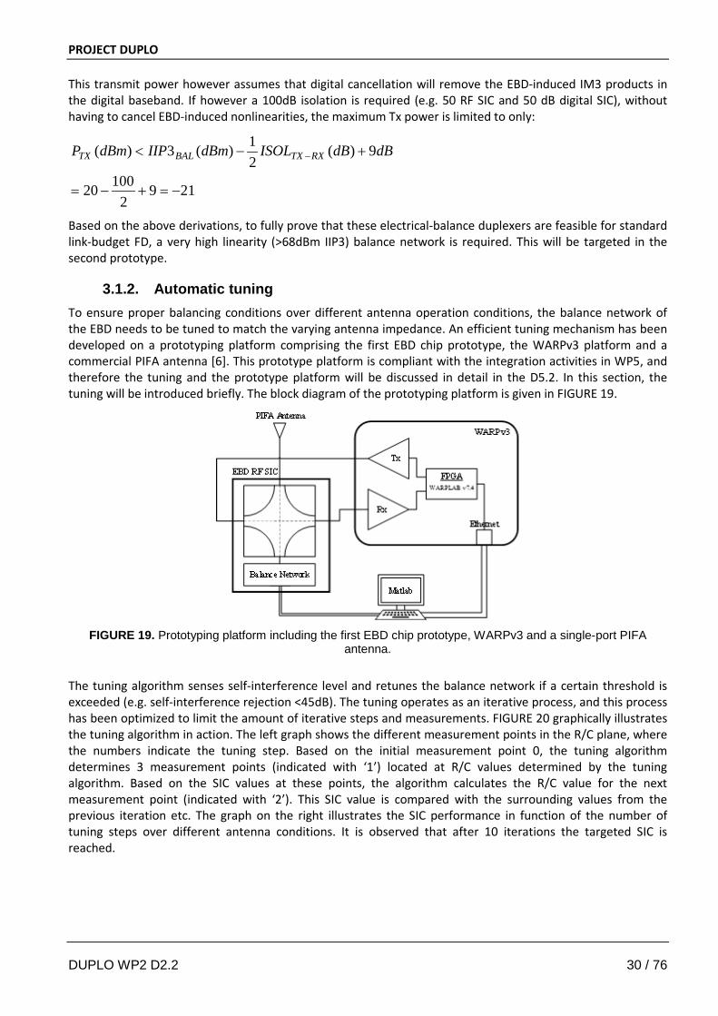
3.1.2. Automatic tuning To ensure proper balancing conditions over different antenna operation conditions, the balance network of the EBD needs to be tuned to match the varying antenna impedance. An efficient tuning mechanism has been developed on a prototyping platform comprising the first EBD chip prototype, the WARPv3 platform and a commercial PIFA antenna [6]. This prototype platform is compliant with the integration activities in WP5, and therefore the tuning and the prototype platform will be discussed in detail in the D5.2. In this section, the tuning will be introduced briefly. The block diagram of the prototyping platform is given in FIGURE 19.
FIGURE 19. Prototyping platform including the first EBD chip prototype, WARPv3 and a single-port PIFA
antenna.
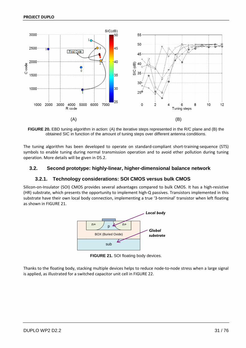
The tuning algorithm senses self-interference level and retunes the balance network if a certain threshold is exceeded (e.g. self-interference rejection <45dB). The tuning operates as an iterative process, and this process has been optimized to limit the amount of iterative steps and measurements. FIGURE 20 graphically illustrates the tuning algorithm in action. The left graph shows the different measurement points in the R/C plane, where the numbers indicate the tuning step. Based on the initial measurement point 0, the tuning algorithm determines 3 measurement points (indicated with ‘1’) located at R/C values determined by the tuning algorithm. Based on the SIC values at these points, the algorithm calculates the R/C value for the next measurement point (indicated with ‘2’). This SIC value is compared with the surrounding values from the previous iteration etc. The graph on the right illustrates the SIC performance in function of the number of tuning steps over different antenna conditions. It is observed that after 10 iterations the targeted SIC is reached.
DUPLO WP2 D2.2 30 / 76
PROJECT DUPLO
(A) (B)
FIGURE 20. EBD tuning algorithm in action: (A) the iterative steps represented in the R/C plane and (B) the obtained SIC in function of the amount of tuning steps over different antenna conditions.
The tuning algorithm has been developed to operate on standard-compliant short-training-sequence (STS) symbols to enable tuning during normal transmission operation and to avoid ether pollution during tuning operation. More details will be given in D5.2.
3.2. Second prototype: highly-linear, higher-dimensional balance network
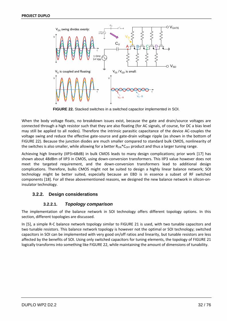
3.2.1. Technology considerations: SOI CMOS versus bulk CMOS Silicon-on-Insulator (SOI) CMOS provides several advantages compared to bulk CMOS. It has a high-resistive (HR) substrate, which presents the opportunity to implement high-Q passives. Transistors implemented in this substrate have their own local body connection, implementing a true ‘3-terminal’ transistor when left floating as shown in FIGURE 21.
n+ n+
BOX (Buried Oxide)
p
sub
Local body
Global substrate
FIGURE 21. SOI floating body devices.
Thanks to the floating body, stacking multiple devices helps to reduce node-to-node stress when a large signal is applied, as illustrated for a switched capacitor unit cell in FIGURE 22.
DUPLO WP2 D2.2 31 / 76
PROJECT DUPLO
t
V
t
V
t
V
VG - BVG - A
1 GHz14 Vpp
VGATE
VSD
A B C DCU
VG
VDS swing divides evenly:
VG is coupled and floating: VGS / VGD is small:
1 GHz14 Vpp
CU
FIGURE 22. Stacked switches in a switched capacitor implemented in SOI.
When the body voltage floats, no breakdown issues exist, because the gate and drain/source voltages are connected through a high resistor such that they are also floating (for AC signals, of course, for DC a bias level may still be applied to all nodes). Therefore the intrinsic parasitic capacitance of the device AC-couples the voltage swing and reduce the effective gate-source and gate-drain voltage ripple (as shown in the bottom of FIGURE 22). Because the junction diodes are much smaller compared to standard bulk CMOS, nonlinearity of the switches is also smaller, while allowing for a better RON*COFF product and thus a larger tuning range.
Achieving high linearity (IIP3>68dB) in bulk CMOS leads to many design complications; prior work [17] has shown about 48dBm of IIP3 in CMOS, using down-conversion transformers. This IIP3 value however does not meet the targeted requirement, and the down-conversion transformers lead to additional design complications. Therefore, bulks CMOS might not be suited to design a highly linear balance network; SOI technology might be better suited, especially because an EBD is in essence a subset of RF switched components [18]. For all these abovementioned reasons, we designed the new balance network in silicon-on-insulator technology.
3.2.2. Design considerations
3.2.2.1. Topology comparison The implementation of the balance network in SOI technology offers different topology options. In this section, different topologies are discussed.
In [5], a simple R-C balance network topology similar to FIGURE 21 is used, with two tunable capacitors and two tunable resistors. This balance network topology is however not the optimal or SOI technology; switched capacitors in SOI can be implemented with very good on/off ratios and linearity, but tunable resistors are less affected by the benefits of SOI. Using only switched capacitors for tuning elements, the topology of FIGURE 21 logically transforms into something like FIGURE 22, while maintaining the amount of dimensions of tunability.
DUPLO WP2 D2.2 32 / 76
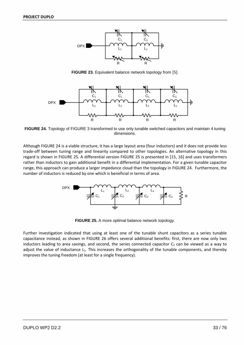
PROJECT DUPLO
L1 L1
C1 C1
R R
DPX
FIGURE 23. Equivalent balance network topology from [5].
L1 L1 L1 L1
C1 C1 C1 C1
R R R R
DPX
FIGURE 24. Topology of FIGURE 3 transformed to use only tunable switched capacitors and maintain 4 tuning
dimensions.
Although FIGURE 24 is a viable structure, it has a large layout area (four inductors) and it does not provide less trade-off between tuning range and linearity compared to other topologies. An alternative topology in this regard is shown in FIGURE 25. A differential version FIGURE 25 is presented in [15, 16] and uses transformers rather than inductors to gain additional benefit in a differential implementation. For a given tunable capacitor range, this approach can produce a larger impedance cloud than the topology in FIGURE 24. Furthermore, the number of inductors is reduced by one which is beneficial in terms of area.
C1 C3 C4
DPX L2 L3
RC2
L1
FIGURE 25. A more optimal balance network topology.
Further investigation indicated that using at least one of the tunable shunt capacitors as a series tunable capacitance instead, as shown in FIGURE 26 offers several additional benefits: first, there are now only two inductors leading to area savings, and second, the series connected capacitor C2 can be viewed as a way to adjust the value of inductance L1. This increases the orthogonality of the tunable components, and thereby improves the tuning freedom (at least for a single frequency).
DUPLO WP2 D2.2 33 / 76
PROJECT DUPLO
C1 C3 C4
DPX L1 L2
R
C2
FIGURE 26. Final topology as used in this design.
For this design project, design target equals a VSWR ≈ 1.5, and a linearity >68dBm IIP3. We found that a tuning range of approximately 1pF each for C1 – C4 will be sufficient for this and the topology of FIGURE 26 produces a good and fairly round impedance cloud when visualized on a Smith chart. Final top-level simulations of this design suggest that the simulated linearity from the balance network matches the system level specifications. Compared to the first prototype, this topology offers about twice as much tuning range.
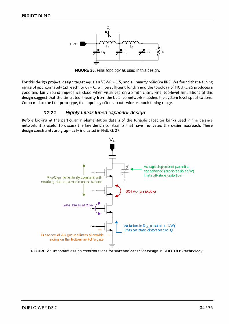
3.2.2.2. Highly linear tuned capacitor design Before looking at the particular implementation details of the tunable capacitor banks used in the balance network, it is useful to discuss the key design constraints that have motivated the design approach. These design constraints are graphically indicated in FIGURE 27.
VA
SOI VDS breakdown
Gate stress at 2.5V
Voltage dependent parasitic capacitance (proportional to W) limits off-state distortion
Variation in RON (related to 1/W) limits on-state distortion and Q
Presence of AC ground limits allowable swing on the bottom switch’s gate
RON/COFF not entirely constant with stacking due to parasitic capacitances
FIGURE 27. Important design considerations for switched capacitor design in SOI CMOS technology.
DUPLO WP2 D2.2 34 / 76
PROJECT DUPLO The ultimate design goal of the balance network switched capacitor is to minimize its distortion, maximize its Ron/Coff, and to avoid over-stressing the devices. Some of the design tradeoffs that limit this goal are:
• In this SOI process, at least 4 devices need to be stacked to ensure stable off-state operation, and avoid drain-source voltage breakdown for 27dBm Tx power in the balance network.
• Ideally, transistor stacking can be done independent of RON/COFF. In reality, the parasitic capacitances present mean that RON/COFF degrades with more stacking.
• Due to voltage division from the parasitic capacitances present, voltage will not be divided evenly between all transistors in the stack. For relatively small unit cells used in a bank, this is be a bigger problem than in the case of a large RF switch. This requires a re-examination of the assumption that four stacked transistors are sufficient for the VDS breakdown issue. It also means that for this application there is little benefit in stacking more transistors than absolutely necessary.
• Most of the nodes in the switch stack can be given a DC bias to ensure that a large swing can be tolerated in the off-state without channel conduction (provided that there is sufficient AC coupling present). However, the source node of the bottom-most transistor in the stack is connected to an AC and DC short. The swing on the gate of this bottom transistor must therefore never exceed VT.
• Sizing of the transistors is constrained by two opposing sources of non-linearity. In the off-state, non-linearity is generated by the voltage-dependent parasitic capacitances present in the switch layout. When the transistor width is increased, these parasitics increase, and linearity degrades. Therefore, the off-state operation prefers as small of switches as possible (but also with as good of AC coupling as possible). In the on-state, the non-linearity of the VDS / IDS transfer characteristic of the switches generates distortion. This signal-dependent channel resistance is reduced by increasing the width of the devices. Therefore, the on-state operation prefers large switches.
• For some specific width used, the distortion due to each effect is equal. Since extremely high Q is not necessary in the balance network design, in most cases we can simply find this particular width and accept the on-state/off-state Qs that result.
• Switch stacking in SOI only works under the assumption that the AC coupling of gate, source, drain, and bulk junctions is much stronger than the coupling of these terminals to ground via parasitics. In the design of a capacitor bank, where tunable elements must oftentimes be relatively small, but routing parasitics don’t necessarily decrease accordingly, this is not always a valid assumption. If there is insufficient AC coupling, voltage will be unevenly divided across the switches in the stack, and the upper limit on how many switches can be stacked with any benefit is reduced. The important implication here is that if coupling is too weak, no amount of stacking will be able to provide enough voltage division to meet the VDS breakdown constraint - a likely scenario for the LSB elements in our capacitor design.
DUPLO WP2 D2.2 35 / 76
PROJECT DUPLO To address many of the design concerns discussed above, the switched capacitor structure of FIGURE 28 has been developed.
CU
CU
V2VB VSD
V1
VG
RG
RB
RSD
CC
FIGURE 28. Unit cell design employed in tunable capacitors.
This unit cell topology has the following key features:
• The placement of unit capacitors (CU) on both ends of the switch transistors provides two benefits. First, it allows the cell to be connected either single-ended or differentially. For our chosen balance network topology we have both series and shunt capacitances, so this flexibility is necessary. Second, this solves the problems associated with the bottom-most transistor in the stack of FIGURE 27, and allows all internal nodes to be set with a DC bias but effectively floating at the frequencies of interest. Although this approach requires four times as much physical capacitance for the same effective switched capacitance, the capacitor models available to us at the time of this design indicate that the fundamental linearity limitation in this design is the switches, not the capacitors.
• Additional coupling capacitors (CC) are placed in parallel with each of the switches. This explicit coupling adds to the intrinsic coupling, and causes the voltage swing in the off-state to be more evenly distributed across all four switches. In the on-state, the capacitors are shorted and there is little effect. For the MSB elements in the capacitor, the intrinsic coupling capacitance is relatively large and the addition of this additional CC has only a minor benefit. However, for the LSB elements in the capacitor bank, where the parasitics are larger relative to the intrinsic coupling, these coupling capacitors make an important difference in improving the efficiency and robustness of the switch design. The presence of all this extra capacitance comes at some cost in terms of CON/COFF ratio. However, using only the minimum capacitor size allowed by the process (33fF) significant benefit can
DUPLO WP2 D2.2 36 / 76
PROJECT DUPLO
be achieved with only about 15% reduction in CON/COFF. Furthermore, in this design, CON – COFF matters and we can compensate for a lower CON/COFF in other ways without any penalty. Finally, CC can be placed directly over the switch transistors in layout. This means that the vast majority of CC’s parasitics will couple into the gate, drain, and source nodes of the underlying transistor structure, which is what we seek to increase the coupling of anyway. Effectively, this leads to zero unwanted parasitics.
• All four terminals of the switch transistors are biased with high-impedance DC biases. For RF applications, it is much better to provide a fixed DC level (while still allowing the body to be seen as a floating node at the RF frequencies of interest). It was reported in [18] that a body-contacted FET in IBM SOI technology can have as much as 20dB better harmonic distortion performance compared to a floating-body counterpart. For this reason, it is clearly better to use body-contacted devices for our application which requires maximum linearity. Although the body contacted FET requires a larger layout footprint and has more parasitics, this is more an issue for digital gates than the moderate sized switches that we’re using. In our case, the area and parasitic penalties are very minor.
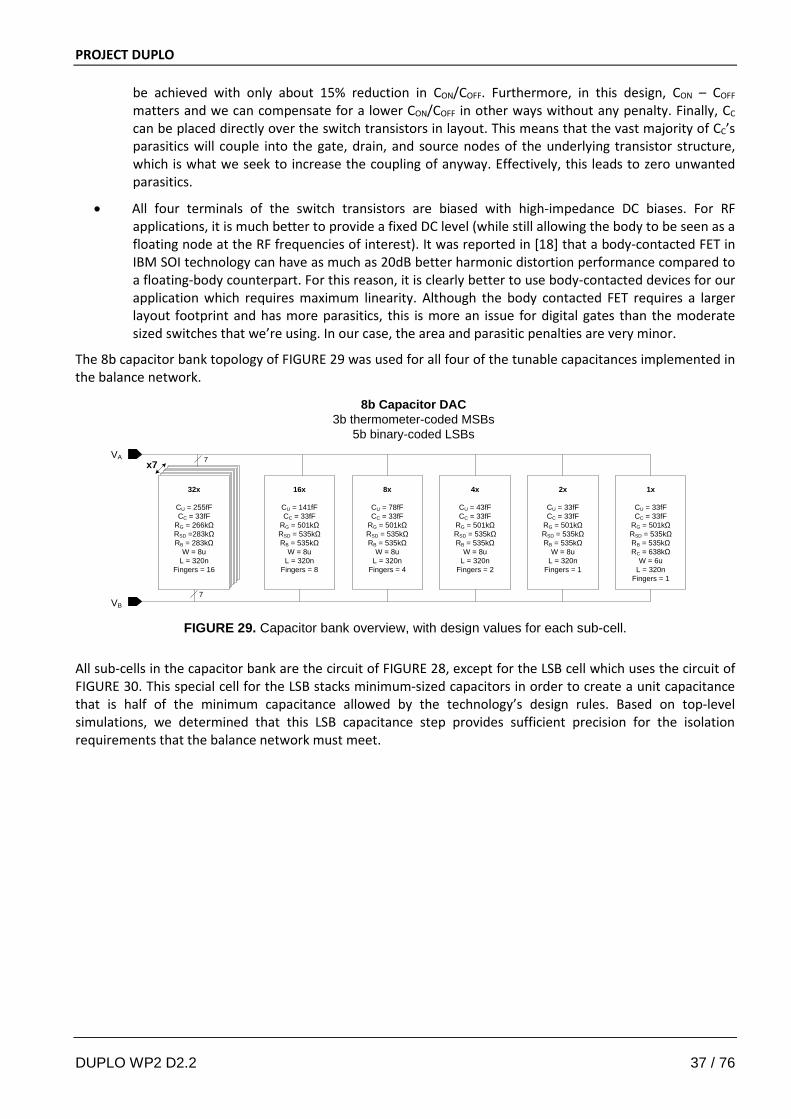
The 8b capacitor bank topology of FIGURE 29 was used for all four of the tunable capacitances implemented in the balance network.
x16
CU = 255fFCC = 33fF
RG = 266kΩRSD =283kΩRB = 283kΩ
W = 8uL = 320n
Fingers = 16
x16
CU = 255fFCC = 33fF
RG = 266kΩRSD =283kΩRB = 283kΩ
W = 8uL = 320n
Fingers = 16
x16
CU = 255fFCC = 33fF
RG = 266kΩRSD =283kΩRB = 283kΩ
W = 8uL = 320n
Fingers = 16
x16
CU = 255fFCC = 33fF
RG = 266kΩRSD =283kΩRB = 283kΩ
W = 8uL = 320n
Fingers = 16
x16
CU = 255fFCC = 33fF
RG = 266kΩRSD =283kΩRB = 283kΩ
W = 8uL = 320n
Fingers = 16
x16
CU = 255fFCC = 33fF
RG = 266kΩRSD =283kΩRB = 283kΩ
W = 8uL = 320n
Fingers = 16
x16
CU = 255fFCC = 33fF
RG = 266kΩRSD =283kΩRB = 283kΩ
W = 8uL = 320n
Fingers = 16
32x
CU = 255fFCC = 33fF
RG = 266kΩRSD =283kΩRB = 283kΩ
W = 8uL = 320n
Fingers = 16
x7
16x
CU = 141fFCC = 33fF
RG = 501kΩRSD = 535kΩRB = 535kΩ
W = 8uL = 320n
Fingers = 8
8x
CU = 78fFCC = 33fF
RG = 501kΩRSD = 535kΩRB = 535kΩ
W = 8uL = 320n
Fingers = 4
4x
CU = 43fFCC = 33fF
RG = 501kΩRSD = 535kΩRB = 535kΩ
W = 8uL = 320n
Fingers = 2
2x
CU = 33fFCC = 33fF
RG = 501kΩRSD = 535kΩRB = 535kΩ
W = 8uL = 320n
Fingers = 1
1x
CU = 33fFCC = 33fF
RG = 501kΩRSD = 535kΩRB = 535kΩRC = 638kΩ
W = 6uL = 320n
Fingers = 1
8b Capacitor DAC3b thermometer-coded MSBs
5b binary-coded LSBs
7
7VA
VB FIGURE 29. Capacitor bank overview, with design values for each sub-cell.
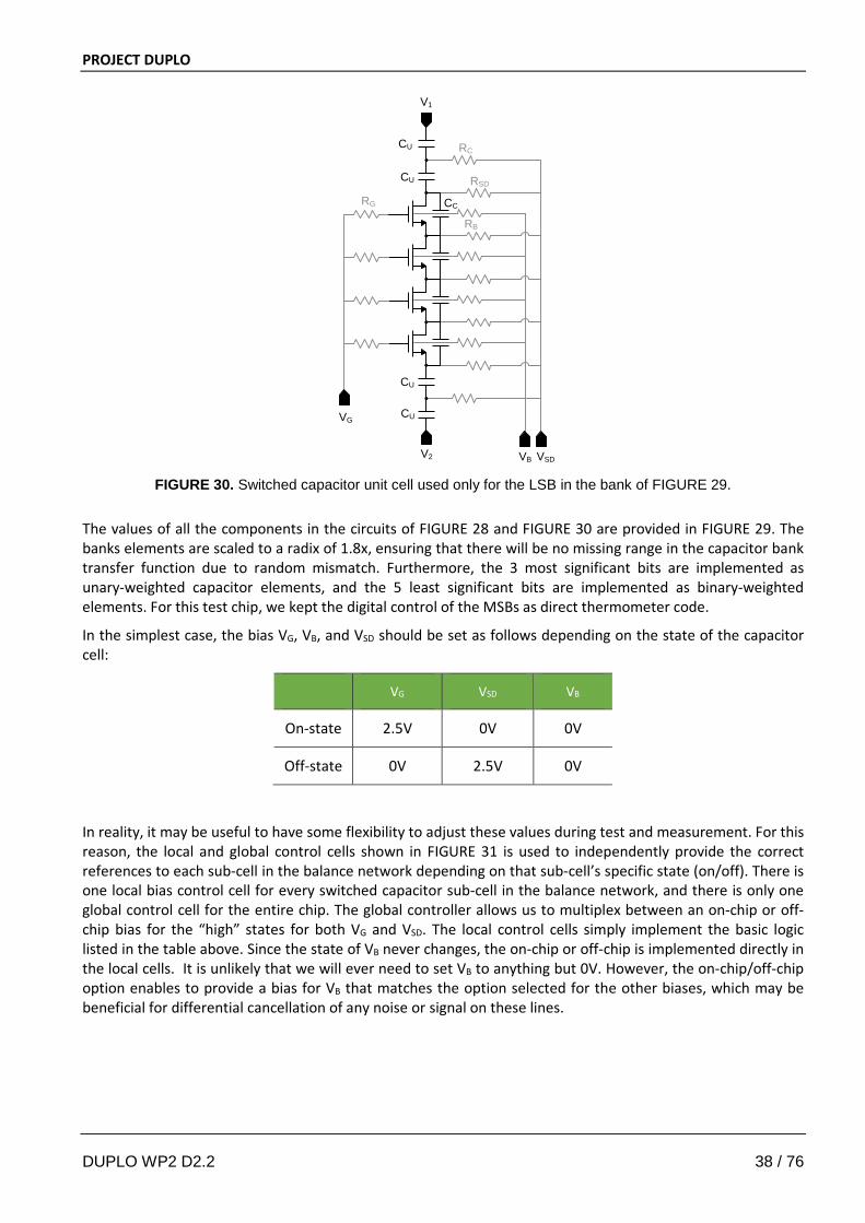
All sub-cells in the capacitor bank are the circuit of FIGURE 28, except for the LSB cell which uses the circuit of FIGURE 30. This special cell for the LSB stacks minimum-sized capacitors in order to create a unit capacitance that is half of the minimum capacitance allowed by the technology’s design rules. Based on top-level simulations, we determined that this LSB capacitance step provides sufficient precision for the isolation requirements that the balance network must meet.
DUPLO WP2 D2.2 37 / 76
PROJECT DUPLO
CU
CU
V2 VB VSD
V1
VG
RG
RB
RSD
CC
RCCU
CU
FIGURE 30. Switched capacitor unit cell used only for the LSB in the bank of FIGURE 29.
The values of all the components in the circuits of FIGURE 28 and FIGURE 30 are provided in FIGURE 29. The banks elements are scaled to a radix of 1.8x, ensuring that there will be no missing range in the capacitor bank transfer function due to random mismatch. Furthermore, the 3 most significant bits are implemented as unary-weighted capacitor elements, and the 5 least significant bits are implemented as binary-weighted elements. For this test chip, we kept the digital control of the MSBs as direct thermometer code.
In the simplest case, the bias VG, VB, and VSD should be set as follows depending on the state of the capacitor cell:
VG VSD VB
On-state 2.5V 0V 0V
Off-state 0V 2.5V 0V
In reality, it may be useful to have some flexibility to adjust these values during test and measurement. For this reason, the local and global control cells shown in FIGURE 31 is used to independently provide the correct references to each sub-cell in the balance network depending on that sub-cell’s specific state (on/off). There is one local bias control cell for every switched capacitor sub-cell in the balance network, and there is only one global control cell for the entire chip. The global controller allows us to multiplex between an on-chip or off-chip bias for the “high” states for both VG and VSD. The local control cells simply implement the basic logic listed in the table above. Since the state of VB never changes, the on-chip or off-chip is implemented directly in the local cells. It is unlikely that we will ever need to set VB to anything but 0V. However, the on-chip/off-chip option enables to provide a bias for VB that matches the option selected for the other biases, which may be beneficial for differential cancellation of any noise or signal on these lines.
DUPLO WP2 D2.2 38 / 76
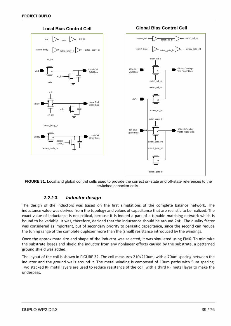
PROJECT DUPLO
en_int
en_int
enb
Vsd
enb
enb
en_int
Vgate
exten_body_b
exten_body_b
exten_body_int
Vbody
Local Cell Gate Bias
Local Cell Body Bias
Local Cell S/D Bias
en enben_int
exten_body exten_body_b exten_body_int exten_gate exten_gate_b exten_gate_int
exten_sd exten_sd_bexten_sd_int
exten_sd_int
Off-chipVsd Bias
Global On-chip Vsd “high” Bias
VDD
Off-chipVgate Bias
Global On-chip Vgate “high” Bias
exten_sd_b
exten_sd_int
exten_sd_b
exten_gate_int
exten_gate_b
exten_gate_b
exten_gate_int
Local Bias Control Cell Global Bias Control Cell
FIGURE 31. Local and global control cells used to provide the correct on-state and off-state references to the
switched capacitor cells.
3.2.2.3. Inductor design The design of the inductors was based on the first simulations of the complete balance network. The inductance value was derived from the topology and values of capacitance that are realistic to be realized. The exact value of inductance is not critical, because it is indeed a part of a tunable matching network which is bound to be variable. It was, therefore, decided that the inductance should be around 2nH. The quality factor was considered as important, but of secondary priority to parasitic capacitance, since the second can reduce the tuning range of the complete duplexer more than the (small) resistance introduced by the windings.
Once the approximate size and shape of the inductor was selected, it was simulated using EMX. To minimize the substrate losses and shield the inductor from any nonlinear effects caused by the substrate, a patterned ground shield was added.
The layout of the coil is shown in FIGURE 32. The coil measures 210x210um, with a 70um spacing between the inductor and the ground walls around it. The metal winding is composed of 10um paths with 5um spacing. Two stacked RF metal layers are used to reduce resistance of the coil, with a third RF metal layer to make the underpass.
DUPLO WP2 D2.2 39 / 76
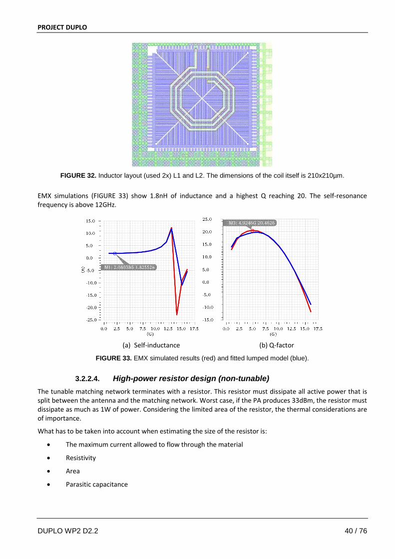
PROJECT DUPLO
FIGURE 32. Inductor layout (used 2x) L1 and L2. The dimensions of the coil itself is 210x210µm.
EMX simulations (FIGURE 33) show 1.8nH of inductance and a highest Q reaching 20. The self-resonance frequency is above 12GHz.
(a) Self-inductance (b) Q-factor
FIGURE 33. EMX simulated results (red) and fitted lumped model (blue).
3.2.2.4. High-power resistor design (non-tunable) The tunable matching network terminates with a resistor. This resistor must dissipate all active power that is split between the antenna and the matching network. Worst case, if the PA produces 33dBm, the resistor must dissipate as much as 1W of power. Considering the limited area of the resistor, the thermal considerations are of importance.
What has to be taken into account when estimating the size of the resistor is:
• The maximum current allowed to flow through the material
• Resistivity
• Area
• Parasitic capacitance
DUPLO WP2 D2.2 40 / 76

PROJECT DUPLO
• Increase of temperature due to dissipated power
• Area of metal connections
• Decrease in electromigration lifetime of surrounding metals due to heating
The options using aluminum or copper metallization are all resulting in extremely large resistors (>500x500um) which eliminates them from the list of possible solutions.
From the available options it was decided that the simplest polysilicon resistor with salicidation is the best option for our application, because:
• The resistivity allows for a rather square area of the resistor. A very long resistor (low resistivity) would be limited by allowed current per unit width. A highly resistive material (no silicidation) has reduced current allowance which would further increase the area and dramatically increase parasitic capacitance.
• Maximum allowed current per unit width is low, but still 3x higher than for the resistor without salicidation.
• In realization of a 50 Ohm resistor the parasitic capacitance is acceptable.
In general, the amount of power to be dissipated in a certain resistance defines the current to be handled by the resistor. This sets the minimum width of the resistor. Once the area (width and length) of the resistor is known, the parasitic capacitance and the temperature increase can be computed.
Increase in temperature around the resistor decreases the electromigration-safe currents of the neighboring metallization. This means that all the contacts and lines feeding the resistor must be wide enough to survive the given amount of current at the given (increased) temperature. This also sets the limit for the resistor option – a low-resistive material would yield a narrow and long resistor with small area for contacts.
As a rough calculation has been performed to check the allowed RMS current through the metal layers.
Fortunately, the electromigration rules allow much higher AC currents (as in this application) than DC currents.
Depending on the power to be dissipated and the maximum parasitic capacitance to be handled, the size of the resistor changes. Below the sizes are given for three levels of power:
• 24dBm = 0,25W R = 50 : IRMS = 70mA, W: 235um, L:36,8um Tincrease: 166 degrees Celsius;
• 27dBm = 0,5W R = 50 : IRMS = 100mA, W: 333um, L:52um Tincrease: 100 degrees Celsius;
• 30dBm = 1W R = 50 : IRMS = 141mA, W: 471um, L:74um Tincrease: 61 degrees Celsius.
The implemented resistor was scaled to W:345um and L = 53um, so there is some margin on handling 0.5W of power. This also amounts to the maximum voltage stress that the tuned capacitors in the balance network can handle.
DUPLO WP2 D2.2 41 / 76
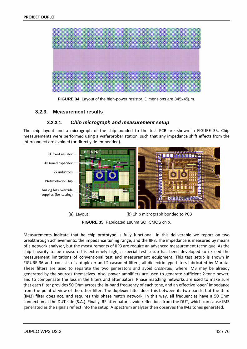
PROJECT DUPLO
FIGURE 34. Layout of the high-power resistor. Dimensions are 345x45μm.
3.2.3. Measurement results
3.2.3.1. Chip micrograph and measurement setup The chip layout and a micrograph of the chip bonded to the test PCB are shown in FIGURE 35. Chip measurements were performed using a waferprober station, such that any impedance shift effects from the interconnect are avoided (or directly de-embedded).
RF fixed resistor
4x tuned capacitor
2x inductors
Network-on-Chip
Analog bias override supplies (for testing)
RF INPUT
(a) Layout (b) Chip micrograph bonded to PCB
FIGURE 35. Fabricated 180nm SOI CMOS chip.
Measurements indicate that he chip prototype is fully functional. In this deliverable we report on two breakthrough achievements: the impedance tuning range, and the IIP3. The impedance is measured by means of a network analyser, but the measurements of IIP3 are require an advanced measurement technique. As the chip linearity to be measured is extremely high, a special test setup has been developed to exceed the measurement limitations of conventional test and measurement equipment. This test setup is shown in FIGURE 36 and consists of a duplexer and 2 cascaded filters, all dielectric type filters fabricated by Murata. These filters are used to separate the two generators and avoid cross-talk, where IM3 may be already generated by the sources themselves. Also, power amplifiers are used to generate sufficient 2-tone power, and to compensate the loss in the filters and attenuators. Phase matching networks are used to make sure that each filter provides 50 Ohm across the in-band frequency of each tone, and an effective ‘open’ impedance from the point of view of the other filter. The duplexer filter does this between its two bands, but the third (IM3) filter does not, and requires this phase match network. In this way, all frequencies have a 50 Ohm connection at the DUT side (S.A.). Finally, RF attenuators avoid reflections from the DUT, which can cause IM3 generated as the signals reflect into the setup. A spectrum analyzer then observes the IM3 tones generated.
DUPLO WP2 D2.2 42 / 76
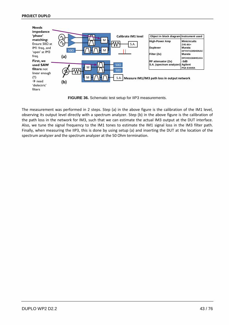
PROJECT DUPLO
FIGURE 36. Schematic test setup for IIP3 measurements.
The measurement was performed in 2 steps. Step (a) in the above figure is the calibration of the IM1 level, observing its output level directly with a spectrum analyzer. Step (b) in the above figure is the calibration of the path loss in the network for IM3, such that we can estimate the actual IM3 output at the DUT interface. Also, we tune the signal frequency to the IM1 tones to estimate the IM1 signal loss in the IM3 filter path. Finally, when measuring the IIP3, this is done by using setup (a) and inserting the DUT at the location of the spectrum analyzer and the spectrum analyzer at the 50 Ohm termination.
M
M50Ω
M
M
50Ω
50Ω
S.A.
S.A.
Calibrate IM1 level
Measure IM1/IM3 path loss in output network
(a)
(b)
High-Power Amp MinicircuitsZVE-8G+
Duplexer MurataDFYH71G95HDNAC
Filter (2x) MurataDFCH31G84HDJAA
RF attenuator (2x) -3dBS.A. (spectrum analyzer) Agilent
PSA E4440A
Object in block diagram Instrument used
Needs impedance ‘phase’ matching:Ensure 50Ω at IM1 freq., and ‘open’ at IM3 freq.First, we used SAW filters: not linear enough (!!) need ‘dielectric’ filters
DUPLO WP2 D2.2 43 / 76
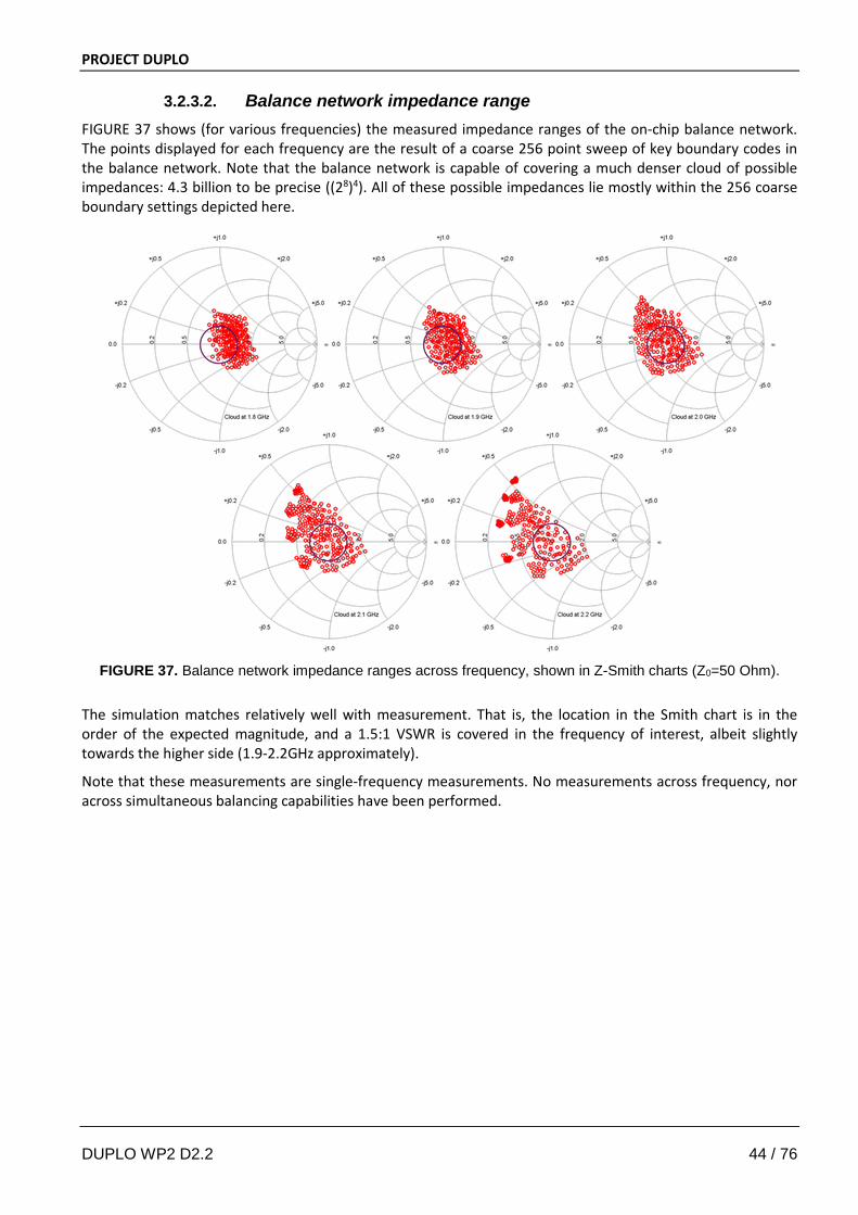
PROJECT DUPLO
3.2.3.2. Balance network impedance range FIGURE 37 shows (for various frequencies) the measured impedance ranges of the on-chip balance network. The points displayed for each frequency are the result of a coarse 256 point sweep of key boundary codes in the balance network. Note that the balance network is capable of covering a much denser cloud of possible impedances: 4.3 billion to be precise ((28)4). All of these possible impedances lie mostly within the 256 coarse boundary settings depicted here.
FIGURE 37. Balance network impedance ranges across frequency, shown in Z-Smith charts (Z0=50 Ohm).
The simulation matches relatively well with measurement. That is, the location in the Smith chart is in the order of the expected magnitude, and a 1.5:1 VSWR is covered in the frequency of interest, albeit slightly towards the higher side (1.9-2.2GHz approximately).
Note that these measurements are single-frequency measurements. No measurements across frequency, nor across simultaneous balancing capabilities have been performed.
DUPLO WP2 D2.2 44 / 76
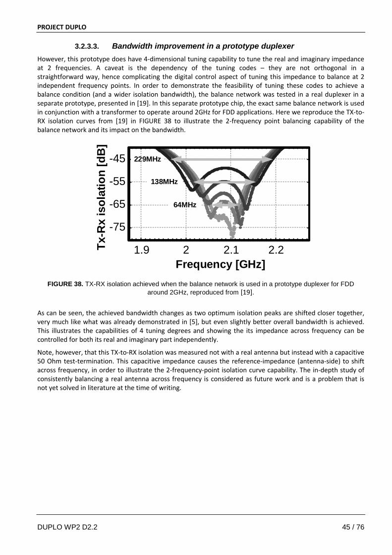
PROJECT DUPLO
3.2.3.3. Bandwidth improvement in a prototype duplexer However, this prototype does have 4-dimensional tuning capability to tune the real and imaginary impedance at 2 frequencies. A caveat is the dependency of the tuning codes – they are not orthogonal in a straightforward way, hence complicating the digital control aspect of tuning this impedance to balance at 2 independent frequency points. In order to demonstrate the feasibility of tuning these codes to achieve a balance condition (and a wider isolation bandwidth), the balance network was tested in a real duplexer in a separate prototype, presented in [19]. In this separate prototype chip, the exact same balance network is used in conjunction with a transformer to operate around 2GHz for FDD applications. Here we reproduce the TX-to-RX isolation curves from [19] in FIGURE 38 to illustrate the 2-frequency point balancing capability of the balance network and its impact on the bandwidth.
FIGURE 38. TX-RX isolation achieved when the balance network is used in a prototype duplexer for FDD
around 2GHz, reproduced from [19].
As can be seen, the achieved bandwidth changes as two optimum isolation peaks are shifted closer together, very much like what was already demonstrated in [5], but even slightly better overall bandwidth is achieved. This illustrates the capabilities of 4 tuning degrees and showing the its impedance across frequency can be controlled for both its real and imaginary part independently.
Note, however, that this TX-to-RX isolation was measured not with a real antenna but instead with a capacitive 50 Ohm test-termination. This capacitive impedance causes the reference-impedance (antenna-side) to shift across frequency, in order to illustrate the 2-frequency-point isolation curve capability. The in-depth study of consistently balancing a real antenna across frequency is considered as future work and is a problem that is not yet solved in literature at the time of writing.
1.9 2 2.1 2.2
-75
-65
-55
-45
Frequency [GHz]
Tx-R
x is
olat
ion
[dB
]
229MHz
138MHz
64MHz
DUPLO WP2 D2.2 45 / 76
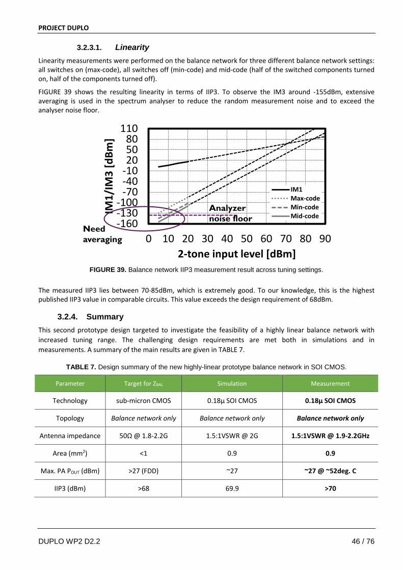
PROJECT DUPLO
3.2.3.1. Linearity Linearity measurements were performed on the balance network for three different balance network settings: all switches on (max-code), all switches off (min-code) and mid-code (half of the switched components turned on, half of the components turned off).
FIGURE 39 shows the resulting linearity in terms of IIP3. To observe the IM3 around -155dBm, extensive averaging is used in the spectrum analyser to reduce the random measurement noise and to exceed the analyser noise floor.
-160-130-100
-70-40-10205080
110
0 10 20 30 40 50 60 70 80 90
IM1/
IM3
[dBm
]
2-tone input level [dBm]
IM1Max-codeMin-codeMid-code
Need averaging
Analyzer noise floor
FIGURE 39. Balance network IIP3 measurement result across tuning settings.
The measured IIP3 lies between 70-85dBm, which is extremely good. To our knowledge, this is the highest published IIP3 value in comparable circuits. This value exceeds the design requirement of 68dBm.
3.2.4. Summary This second prototype design targeted to investigate the feasibility of a highly linear balance network with increased tuning range. The challenging design requirements are met both in simulations and in measurements. A summary of the main results are given in TABLE 7.
TABLE 7. Design summary of the new highly-linear prototype balance network in SOI CMOS.
Parameter Target for ZBAL Simulation Measurement
Technology sub-micron CMOS 0.18μ SOI CMOS 0.18μ SOI CMOS
Topology Balance network only Balance network only Balance network only
Antenna impedance 50Ω @ 1.8-2.2G 1.5:1VSWR @ 2G 1.5:1VSWR @ 1.9-2.2GHz
Area (mm2) <1 0.9 0.9
Max. PA POUT (dBm) >27 (FDD) ~27 ~27 @ ~52deg. C
IIP3 (dBm) >68 69.9 >70
DUPLO WP2 D2.2 46 / 76

PROJECT DUPLO The key performance of this design are:
• Linearity is >70dBm, good enough to have a total system SIC of 100dB without IM3 generated in the balance network limiting performance.
• Impedance tuning ranges have greatly improved with respect to the first prototype. The 4-dimensional tuning implies that there is more freedom to achieve increased isolation bandwidth, keeping in mind that still the antenna impedance variability across frequency might limit the effective functional bandwidth.
• Power handling of the prototype is great, +27dBm can be handled without significantly heating up.
This prototype advances state-of-the-art in tunable RF switched components, including antenna tuners, electrical balance duplexers and RF switches alike.
DUPLO WP2 D2.2 47 / 76
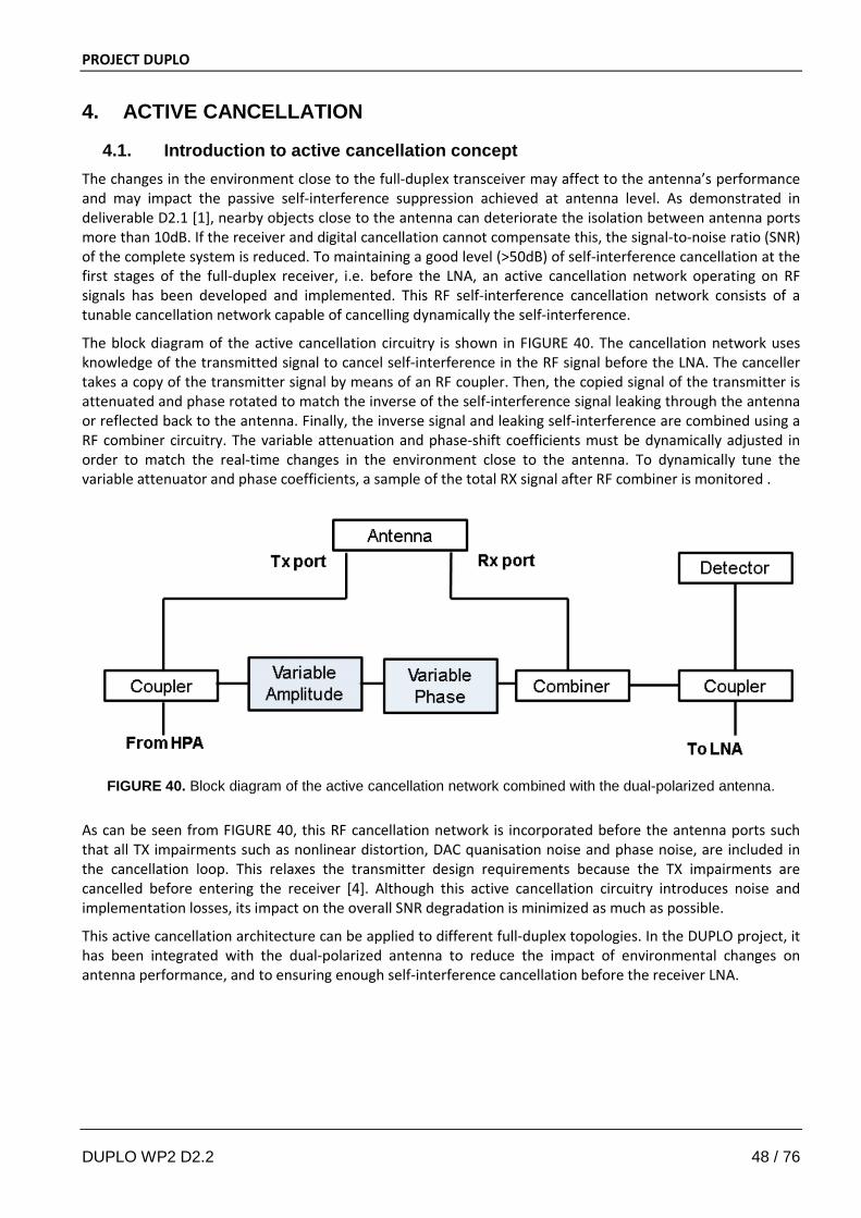
PROJECT DUPLO
4. ACTIVE CANCELLATION
4.1. Introduction to active cancellation concept The changes in the environment close to the full-duplex transceiver may affect to the antenna’s performance and may impact the passive self-interference suppression achieved at antenna level. As demonstrated in deliverable D2.1 [1], nearby objects close to the antenna can deteriorate the isolation between antenna ports more than 10dB. If the receiver and digital cancellation cannot compensate this, the signal-to-noise ratio (SNR) of the complete system is reduced. To maintaining a good level (>50dB) of self-interference cancellation at the first stages of the full-duplex receiver, i.e. before the LNA, an active cancellation network operating on RF signals has been developed and implemented. This RF self-interference cancellation network consists of a tunable cancellation network capable of cancelling dynamically the self-interference.
The block diagram of the active cancellation circuitry is shown in FIGURE 40. The cancellation network uses knowledge of the transmitted signal to cancel self-interference in the RF signal before the LNA. The canceller takes a copy of the transmitter signal by means of an RF coupler. Then, the copied signal of the transmitter is attenuated and phase rotated to match the inverse of the self-interference signal leaking through the antenna or reflected back to the antenna. Finally, the inverse signal and leaking self-interference are combined using a RF combiner circuitry. The variable attenuation and phase-shift coefficients must be dynamically adjusted in order to match the real-time changes in the environment close to the antenna. To dynamically tune the variable attenuator and phase coefficients, a sample of the total RX signal after RF combiner is monitored .
FIGURE 40. Block diagram of the active cancellation network combined with the dual-polarized antenna.
As can be seen from FIGURE 40, this RF cancellation network is incorporated before the antenna ports such that all TX impairments such as nonlinear distortion, DAC quanisation noise and phase noise, are included in the cancellation loop. This relaxes the transmitter design requirements because the TX impairments are cancelled before entering the receiver [4]. Although this active cancellation circuitry introduces noise and implementation losses, its impact on the overall SNR degradation is minimized as much as possible.
This active cancellation architecture can be applied to different full-duplex topologies. In the DUPLO project, it has been integrated with the dual-polarized antenna to reduce the impact of environmental changes on antenna performance, and to ensuring enough self-interference cancellation before the receiver LNA.
DUPLO WP2 D2.2 48 / 76
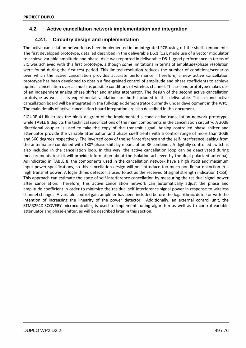
PROJECT DUPLO
4.2. Active cancellation network implementation and integration
4.2.1. Circuitry design and implementation The active cancellation network has been implemented in an integrated PCB using off-the-shelf components. The first developed prototype, detailed described in the deliverable D5.1 [12], made use of a vector modulator to achieve variable amplitude and phase. As it was reported in deliverable D5.1, good performance in terms of SIC was achieved with this first prototype, although some limitations in terms of amplitude/phase resolution were found during the first test period. This limited resolution reduces the number of conditions/scenarios over which the active cancellation provides accurate performance. Therefore, a new active cancellation prototype has been developed to obtain a fine-grained control of amplitude and phase coefficients to achieve optimal cancellation over as much as possible conditions of wireless channel. This second prototype makes use of an independent analog phase shifter and analog attenuator. The design of the second active cancellation prototype as well as its experimental validation are both included in this deliverable. This second active cancellation board will be integrated in the full-duplex demonstrator currently under development in the WP5. The main details of active cancellation board integration are also described in this document.
FIGURE 41 illustrates the block diagram of the implemented second active cancellation network prototype, while TABLE 8 depicts the technical specifications of the main components in the cancellation circuitry. A 20dB directional coupler is used to take the copy of the transmit signal. Analog controlled phase shifter and attenuator provide the variable attenuation and phase coefficients with a control range of more than 30dB and 360 degrees respectively. The inverted copy of the self-interference and the self-interference leaking from the antenna are combined with 180º phase-shift by means of an RF combiner. A digitally controlled switch is also included in the cancellation loop. In this way, the active cancellation loop can be deactivated during measurements test (it will provide information about the isolation achieved by the dual-polarized antenna). As indicated in TABLE 8, the components used in the cancellation network have a high P1dB and maximum input power specifications, so this cancellation design will not introduce too much non-linear distortion in a high transmit power. A logarithmic detector is used to act as the received SI signal strength indication (RSSI). This approach can estimate the state of self-interference cancellation by measuring the residual signal power after cancellation. Therefore, this active cancellation network can automatically adjust the phase and amplitude coefficient in order to minimize the residual self-interference signal power in response to wireless channel changes. A variable control gain amplifier has been included before the logarithmic detector with the intention of increasing the linearity of the power detector. Additionally, an external control unit, the STM32F4DISCOVERY microcontroller, is used to implement tuning algorithm as well as to control variable attenuator and phase-shifter, as will be described later in this section.
DUPLO WP2 D2.2 49 / 76
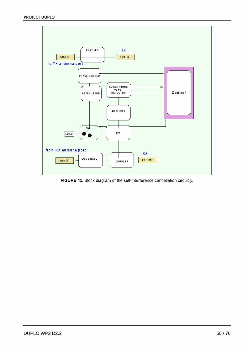
PROJECT DUPLO
C O U P L E R
C O U P L E R
S M A (M )S M A (F )
PH A S E SH IF T E R
C O M B IN A T O RS M A (F )
L O A D
S M A (M )
A M P L IF IE R
to T X a n te n n a p o r t
T x
S W 1
R X
C o n tr o lA T T E N U A T O R
f r o m R X an te n n a p o r t
B P F
L O G A R IT H M ICP O W E R
D E T E C T O R
FIGURE 41. Block diagram of the self-interference cancellation circuitry.
DUPLO WP2 D2.2 50 / 76
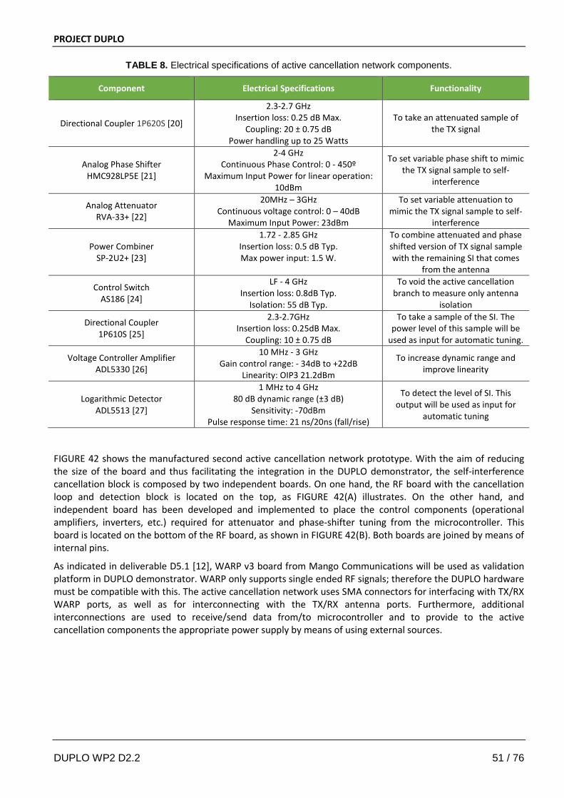
PROJECT DUPLO
TABLE 8. Electrical specifications of active cancellation network components.
Component Electrical Specifications Functionality
Directional Coupler 1P620S [20]
2.3-2.7 GHz Insertion loss: 0.25 dB Max.
Coupling: 20 ± 0.75 dB Power handling up to 25 Watts
To take an attenuated sample of the TX signal
Analog Phase Shifter HMC928LP5E [21]
2-4 GHz Continuous Phase Control: 0 - 450º
Maximum Input Power for linear operation: 10dBm
To set variable phase shift to mimic the TX signal sample to self-
interference
Analog Attenuator RVA-33+ [22]
20MHz – 3GHz Continuous voltage control: 0 – 40dB
Maximum Input Power: 23dBm
To set variable attenuation to mimic the TX signal sample to self-
interference
Power Combiner SP-2U2+ [23]
1.72 - 2.85 GHz Insertion loss: 0.5 dB Typ. Max power input: 1.5 W.
To combine attenuated and phase shifted version of TX signal sample with the remaining SI that comes
from the antenna
Control Switch AS186 [24]
LF - 4 GHz Insertion loss: 0.8dB Typ.
Isolation: 55 dB Typ.
To void the active cancellation branch to measure only antenna
isolation
Directional Coupler 1P610S [25]
2.3-2.7GHz Insertion loss: 0.25dB Max.
Coupling: 10 ± 0.75 dB
To take a sample of the SI. The power level of this sample will be
used as input for automatic tuning.
Voltage Controller Amplifier ADL5330 [26]
10 MHz - 3 GHz Gain control range: - 34dB to +22dB
Linearity: OIP3 21.2dBm
To increase dynamic range and improve linearity
Logarithmic Detector ADL5513 [27]
1 MHz to 4 GHz 80 dB dynamic range (±3 dB)
Sensitivity: -70dBm Pulse response time: 21 ns/20ns (fall/rise)
To detect the level of SI. This output will be used as input for
automatic tuning
FIGURE 42 shows the manufactured second active cancellation network prototype. With the aim of reducing the size of the board and thus facilitating the integration in the DUPLO demonstrator, the self-interference cancellation block is composed by two independent boards. On one hand, the RF board with the cancellation loop and detection block is located on the top, as FIGURE 42(A) illustrates. On the other hand, and independent board has been developed and implemented to place the control components (operational amplifiers, inverters, etc.) required for attenuator and phase-shifter tuning from the microcontroller. This board is located on the bottom of the RF board, as shown in FIGURE 42(B). Both boards are joined by means of internal pins.
As indicated in deliverable D5.1 [12], WARP v3 board from Mango Communications will be used as validation platform in DUPLO demonstrator. WARP only supports single ended RF signals; therefore the DUPLO hardware must be compatible with this. The active cancellation network uses SMA connectors for interfacing with TX/RX WARP ports, as well as for interconnecting with the TX/RX antenna ports. Furthermore, additional interconnections are used to receive/send data from/to microcontroller and to provide to the active cancellation components the appropriate power supply by means of using external sources.
DUPLO WP2 D2.2 51 / 76
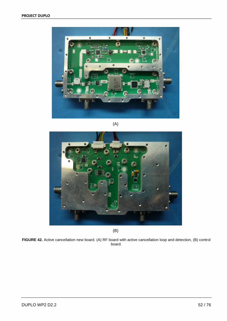
PROJECT DUPLO
(A)
(B)
FIGURE 42. Active cancellation new board. (A) RF board with active cancellation loop and detection, (B) control board.
DUPLO WP2 D2.2 52 / 76
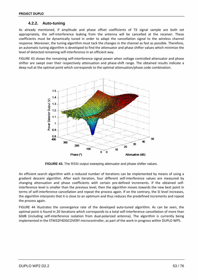
PROJECT DUPLO
4.2.2. Auto-tuning As already mentioned, if amplitude and phase offset coefficients of TX signal sample are both set appropriately, the self-interference leaking from the antenna will be cancelled at the receiver. These coefficients must be dynamically tuned in order to adapt the cancellation signal to the wireless channel response. Moreover, the tuning algorithm must tack the changes in the channel as fast as possible. Therefore, an automatic tuning algorithm is developed to find the attenuator and phase shifter values which minimize the level of detected remaining self-interference in an efficient way.
FIGURE 43 shows the remaining self-interference signal power when voltage controlled attenuator and phase shifter are swept over their respectively attenuation and phase-shift range. The obtained results indicate a deep null at the optimal point which corresponds to the optimal attenuation/phase code combination.
FIGURE 43. The RSSI output sweeping attenuator and phase shifter values.
An efficient search algorithm with a reduced number of iterations can be implemented by means of using a gradient descent algorithm. After each iteration, four different self-interference values are measured by changing attenuation and phase coefficients with certain pre-defined increments. If the obtained self-interference level is smaller than the previous level, then the algorithm moves towards the new best point in terms of self-interference cancellation and repeat the process again. If on the contrary, the SI level increases, the algorithm interprets that it is close to an optimum and thus reduces the predefined increments and repeat the process again.
FIGURE 44 illustrates the convergence rate of the developed auto-tuned algorithm. As can be seen, the optimal point is found in 20 iterations which corresponds to a total self-interference cancellation of more than 60dB (including self-interference isolation from dual-polarized antenna). The algorithm is currently being implemented in the STM32F4DISCOVERY microcontroller, as part of the work in progress within DUPLO WP5.
DUPLO WP2 D2.2 53 / 76
PROJECT DUPLO
FIGURE 44. Converge rate of the developed auto-tuning algorithm.
4.2.3. Integration in DUPLO demonstrator DUPLO project will integrate a full-duplex radio transceiver prototype with the aim of validating the full-duplex proof-of-concept and to quantify the self-interference cancellation performance over the complete system. The SIC solutions investigated within DUPLO WP2 and described in this deliverable will be integrated with different key blocks developed in other work packages of DUPLO project, e.g. digital cancellation block from work package 3. DUPLO project will develop two different radio prototypes targeting two different form factors. The first prototype targets compact form factors and includes the dual-polarized antenna and the active cancellation network. The second prototype targets extremely compact form factor radio devices and integrates the electrical balance circuitry in conjunction with a commercial antenna. Both full-duplex radio transceiver prototypes will be developed using WARP platform and they will operate at the same frequency band.
FIGURE 45 illustrates the block diagram of the DUPLO demonstrator which includes dual-polarized antenna and active cancellation network. As already mentioned, the second prototype of the dual-polarized antenna and the second prototype of the active cancellation network will be integrated in the demonstrator. As can be seen from FIGURE 45, the active cancellation board is externally controlled by means of using the STM32F4DISCOVERY control unit [12]. This microcontroller is used to control variable attenuator and phase-shifter, as well as to implement tuning algorithm. TABLE 9 lists the description of the interface signals between active cancellation board and microcontroller.
Moreover, the active cancellation block is also integrated with validation platform by proper interface definition. In particular, a set of three interface signals has been defined between WARP platform and active cancellation microcontroller in order to facilitate the interoperability between both subsystems, as TABLE 9 lists. The S1 signal will be used to activate active cancellation tuning, while the S2 signal will indicate that active cancellation tuning is finished. The S3 signal will be used to deactivate the active cancellation loop from WARP with the aim of visualize/validate the isolation achieved by only the dual-polarized antenna. The level of these control signals is defined by FPGA I/O voltage, namely 0/2.5 volts. However, the microcontroller works with level signals of 0/3 volts, therefore, a level-shifter has been implemented to convert to appropriate control voltages and to avoid any damage of FPGA pins. Additionally, a common GND line has been also defined between active cancellation network and WARP board, while RF signals will be interconnected among the different subsystems by means of using SMA connectors and RF cables.
DUPLO WP2 D2.2 54 / 76
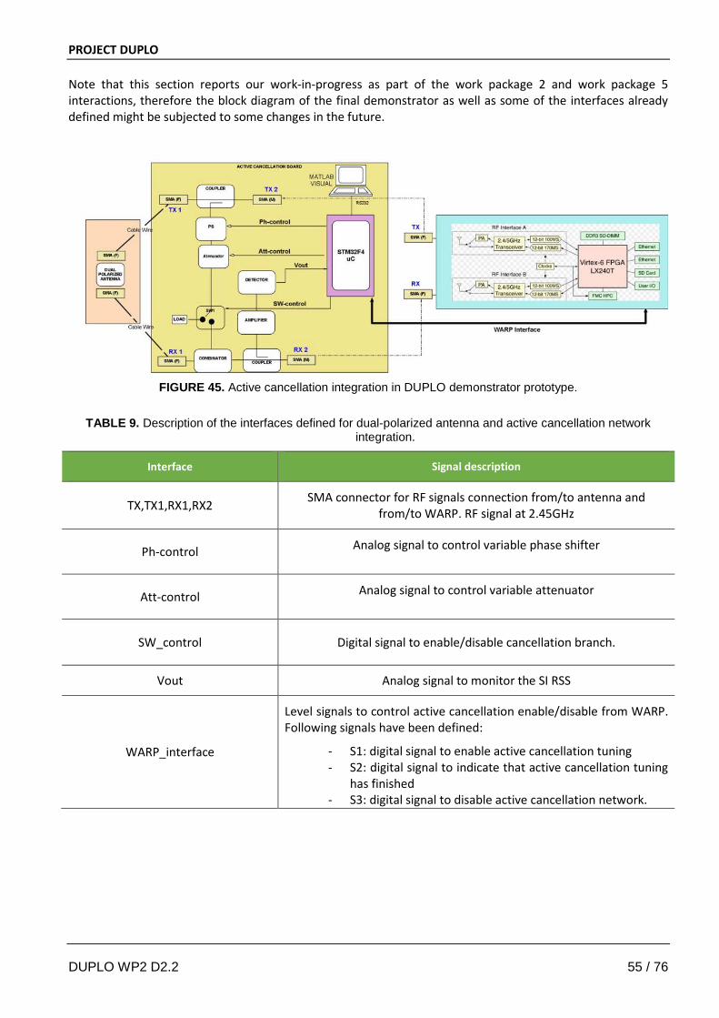
PROJECT DUPLO Note that this section reports our work-in-progress as part of the work package 2 and work package 5 interactions, therefore the block diagram of the final demonstrator as well as some of the interfaces already defined might be subjected to some changes in the future.
FIGURE 45. Active cancellation integration in DUPLO demonstrator prototype.
TABLE 9. Description of the interfaces defined for dual-polarized antenna and active cancellation network integration.
Interface Signal description
TX,TX1,RX1,RX2 SMA connector for RF signals connection from/to antenna and from/to WARP. RF signal at 2.45GHz
Ph-control Analog signal to control variable phase shifter
Att-control Analog signal to control variable attenuator
SW_control Digital signal to enable/disable cancellation branch.
Vout Analog signal to monitor the SI RSS
WARP_interface
Level signals to control active cancellation enable/disable from WARP. Following signals have been defined:
- S1: digital signal to enable active cancellation tuning - S2: digital signal to indicate that active cancellation tuning
has finished - S3: digital signal to disable active cancellation network.
DUPLO WP2 D2.2 55 / 76
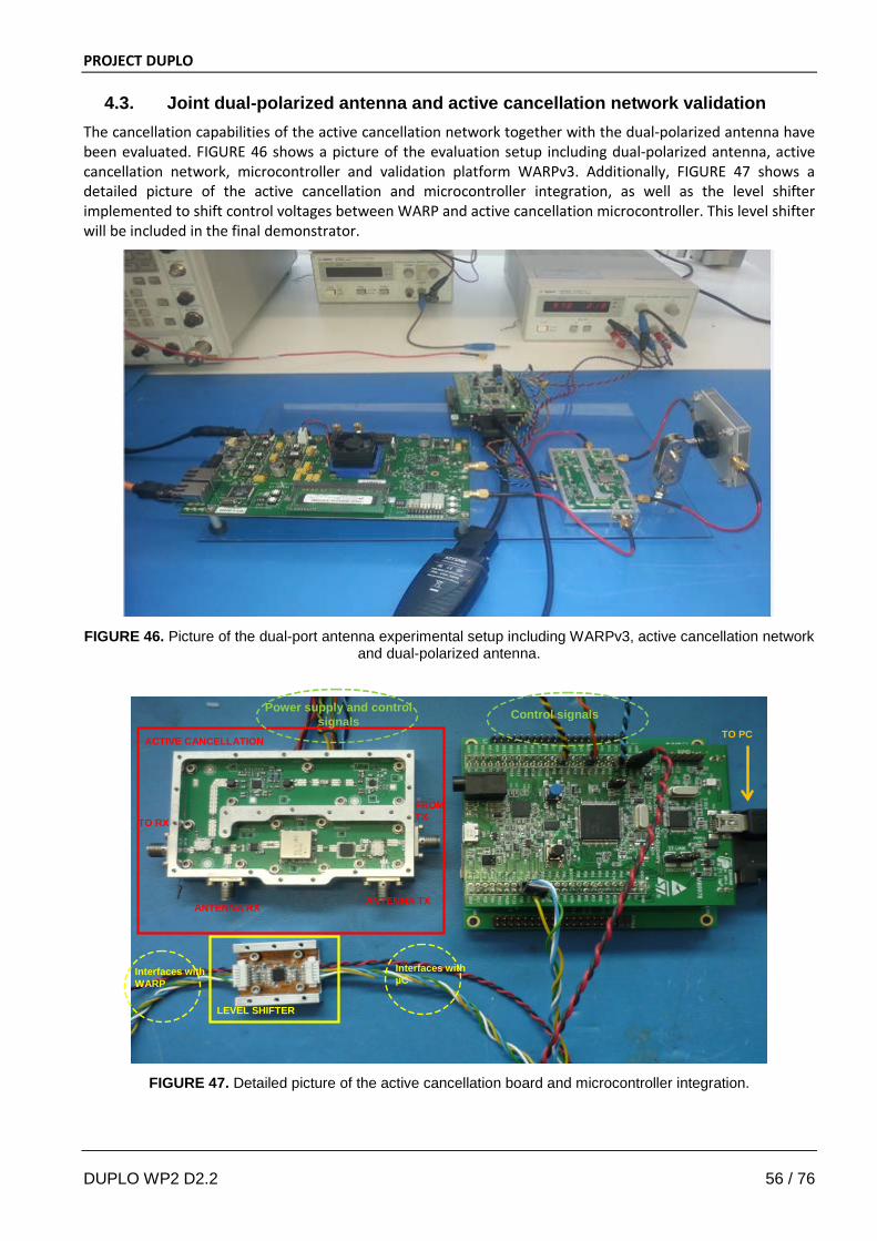
PROJECT DUPLO
4.3. Joint dual-polarized antenna and active cancellation network validation The cancellation capabilities of the active cancellation network together with the dual-polarized antenna have been evaluated. FIGURE 46 shows a picture of the evaluation setup including dual-polarized antenna, active cancellation network, microcontroller and validation platform WARPv3. Additionally, FIGURE 47 shows a detailed picture of the active cancellation and microcontroller integration, as well as the level shifter implemented to shift control voltages between WARP and active cancellation microcontroller. This level shifter will be included in the final demonstrator.
FIGURE 46. Picture of the dual-port antenna experimental setup including WARPv3, active cancellation network
and dual-polarized antenna.
ACTIVE CANCELLATION
FROM TXTO RX
ANTENNA TXANTENNA RX
Power supply and control signals Control signals
TO PC
LEVEL SHIFTER
Interfaces withWARP
Interfaces withµC
ACTIVE CANCELLATION
FROM TXTO RX
ANTENNA TXANTENNA RX
Power supply and control signals Control signals
TO PC
LEVEL SHIFTER
Interfaces withWARP
Interfaces withµC
FIGURE 47. Detailed picture of the active cancellation board and microcontroller integration.
DUPLO WP2 D2.2 56 / 76
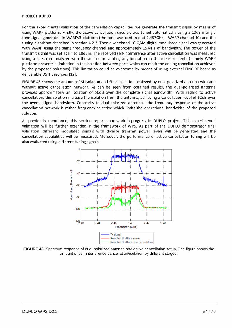
PROJECT DUPLO For the experimental validation of the cancellation capabilities we generate the transmit signal by means of using WARP platform. Firstly, the active cancellation circuitry was tuned automatically using a 10dBm single tone signal generated in WARPv3 platform (the tone was centered at 2.457GHz – WARP channel 10) and the tuning algorithm described in section 4.2.2. Then a wideband 16-QAM digital modulated signal was generated with WARP using the same frequency channel and approximately 15MHz of bandwidth. The power of the transmit signal was set again to 10dBm. The received self-interference after active cancellation was measured using a spectrum analyzer with the aim of preventing any limitation in the measurements (namely WARP platform presents a limitation in the isolation between ports which can mask the analog cancellation achieved by the proposed solutions). This limitation could be overcome by means of using external FMC-RF board as deliverable D5.1 describes [12].
FIGURE 48 shows the amount of SI isolation and SI cancellation achieved by dual-polarized antenna with and without active cancellation network. As can be seen from obtained results, the dual-polarized antenna provides approximately an isolation of 50dB over the complete signal bandwidth. With regard to active cancellation, this solution increase the isolation from the antenna, achieving a cancellation level of 62dB over the overall signal bandwidth. Contrarily to dual-polarized antenna, the frequency response of the active cancellation network is rather frequency selective which limits the operational bandwidth of the proposed solution.
As previously mentioned, this section reports our work-in-progress in DUPLO project. This experimental validation will be further extended in the framework of WP5. As part of the DUPLO demonstrator final validation, different modulated signals with diverse transmit power levels will be generated and the cancellation capabilities will be measured. Moreover, the performance of active cancellation tuning will be also evaluated using different tuning signals.
FIGURE 48. Spectrum response of dual-polarized antenna and active cancellation setup. The figure shows the
amount of self-interference cancellation/isolation by different stages.
DUPLO WP2 D2.2 57 / 76
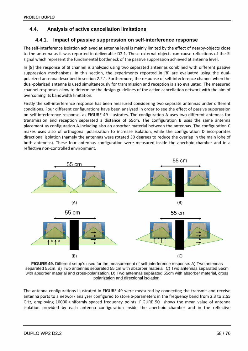
PROJECT DUPLO
4.4. Analysis of active cancellation limitations
4.4.1. Impact of passive suppression on self-interference response The self-interference isolation achieved at antenna level is mainly limited by the effect of nearby-objects close to the antenna as it was reported in deliverable D2.1. These external objects can cause reflections of the SI signal which represent the fundamental bottleneck of the passive suppression achieved at antenna level.
In [8] the response of SI channel is analyzed using two separated antennas combined with different passive suppression mechanisms. In this section, the experiments reported in [8] are evaluated using the dual-polarized antenna described in section 2.2.1. Furthermore, the response of self-interference channel when the dual-polarized antenna is used simultaneously for transmission and reception is also evaluated. The measured channel responses allow to determine the design guidelines of the active cancellation network with the aim of overcoming its bandwidth limitation.
Firstly the self-interference response has been measured considering two separate antennas under different conditions. Four different configurations have been analyzed in order to see the effect of passive suppression on self-interference response, as FIGURE 49 illustrates. The configuration A uses two different antennas for transmission and reception separated a distance of 55cm. The configuration B uses the same antenna placement as configuration A including also an absorber material between the antennas. The configuration C makes uses also of orthogonal polarization to increase isolation, while the configuration D incorporates directional isolation (namely the antennas were rotated 30 degrees to reduce the overlap in the main lobe of both antennas). These four antennas configuration were measured inside the anechoic chamber and in a reflective non-controlled environment.
55 cm
55 cm
(A) (B)
55 cm
55 cm
(B) (C)
FIGURE 49. Different setup’s used for the measurement of self-interference response. A) Two antennas separated 55cm. B) Two antennas separated 55 cm with absorber material. C) Two antennas separated 55cm with absorber material and cross-polarization. D) Two antennas separated 55cm with absorber material, cross
polarization and directional isolation.
The antenna configurations illustrated in FIGURE 49 were measured by connecting the transmit and receive antenna ports to a network analyzer configured to store S-parameters in the frequency band from 2.3 to 2.55 GHz, employing 10000 uniformly spaced frequency points. FIGURE 50 shows the mean value of antenna isolation provided by each antenna configuration inside the anechoic chamber and in the reflective
DUPLO WP2 D2.2 58 / 76
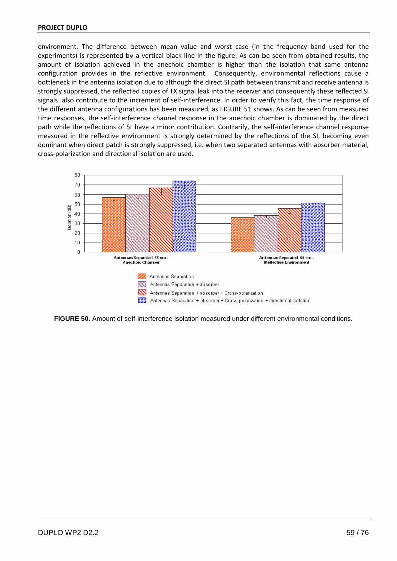
PROJECT DUPLO environment. The difference between mean value and worst case (in the frequency band used for the experiments) is represented by a vertical black line in the figure. As can be seen from obtained results, the amount of isolation achieved in the anechoic chamber is higher than the isolation that same antenna configuration provides in the reflective environment. Consequently, environmental reflections cause a bottleneck in the antenna isolation due to although the direct SI path between transmit and receive antenna is strongly suppressed, the reflected copies of TX signal leak into the receiver and consequently these reflected SI signals also contribute to the increment of self-interference. In order to verify this fact, the time response of the different antenna configurations has been measured, as FIGURE 51 shows. As can be seen from measured time responses, the self-interference channel response in the anechoic chamber is dominated by the direct path while the reflections of SI have a minor contribution. Contrarily, the self-interference channel response measured in the reflective environment is strongly determined by the reflections of the SI, becoming even dominant when direct patch is strongly suppressed, i.e. when two separated antennas with absorber material, cross-polarization and directional isolation are used.
FIGURE 50. Amount of self-interference isolation measured under different environmental conditions.
DUPLO WP2 D2.2 59 / 76
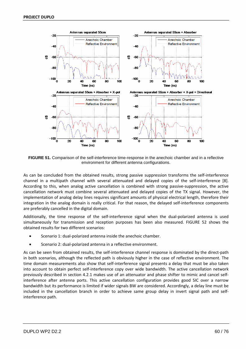
PROJECT DUPLO
FIGURE 51. Comparison of the self-interference time-response in the anechoic chamber and in a reflective
environment for different antenna configurations.
As can be concluded from the obtained results, strong passive suppression transforms the self-interference channel in a multipath channel with several attenuated and delayed copies of the self-interference [8]. According to this, when analog active cancellation is combined with strong passive-suppression, the active cancellation network must combine several attenuated and delayed copies of the TX signal. However, the implementation of analog delay lines requires significant amounts of physical electrical length, therefore their integration in the analog domain is really critical. For that reason, the delayed self-interference components are preferably cancelled in the digital domain.
Additionally, the time response of the self-interference signal when the dual-polarized antenna is used simultaneously for transmission and reception purposes has been also measured. FIGURE 52 shows the obtained results for two different scenarios:
• Scenario 1: dual-polarized antenna inside the anechoic chamber.
• Scenario 2: dual-polarized antenna in a reflective environment.
As can be seen from obtained results, the self-interference channel response is dominated by the direct-path in both scenarios, although the reflected path is obviously higher in the case of reflective environment. The time domain measurements also show that self-interference signal presents a delay that must be also taken into account to obtain perfect self-interference copy over wide bandwidth. The active cancellation network previously described in section 4.2.1 makes use of an attenuator and phase shifter to mimic and cancel self-interference after antenna ports. This active cancellation configuration provides good SIC over a narrow bandwidth but its performance is limited if wider signals BW are considered. Accordingly, a delay line must be included in the cancellation branch in order to achieve same group delay in invert signal path and self-interference path.
DUPLO WP2 D2.2 60 / 76
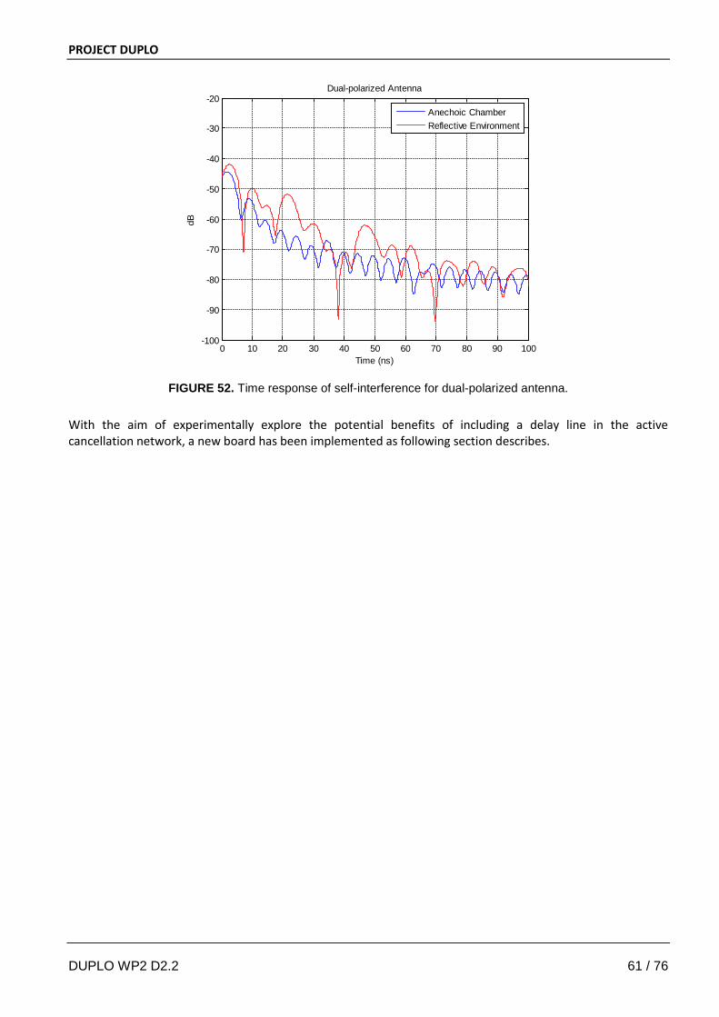
PROJECT DUPLO
0 10 20 30 40 50 60 70 80 90 100-100
-90
-80
-70
-60
-50
-40
-30
-20
Time (ns)
dB
Dual-polarized Antenna
Anechoic ChamberReflective Environment
FIGURE 52. Time response of self-interference for dual-polarized antenna.
With the aim of experimentally explore the potential benefits of including a delay line in the active cancellation network, a new board has been implemented as following section describes.
DUPLO WP2 D2.2 61 / 76
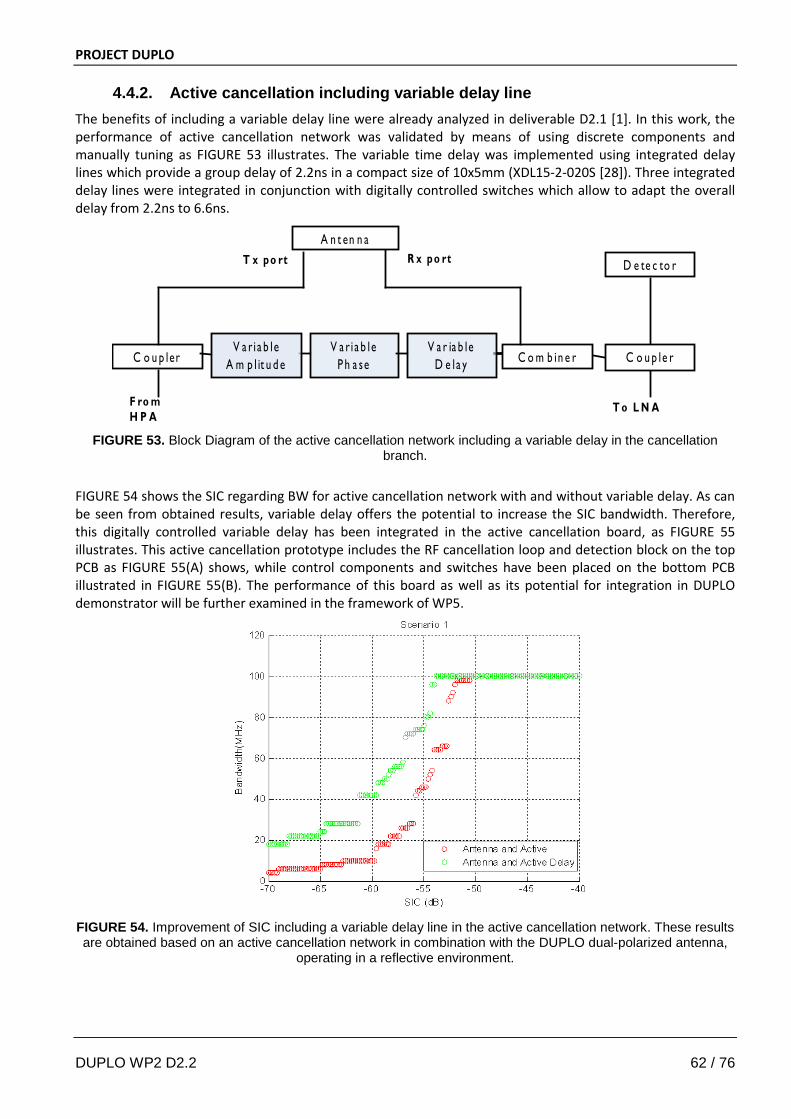
PROJECT DUPLO
4.4.2. Active cancellation including variable delay line The benefits of including a variable delay line were already analyzed in deliverable D2.1 [1]. In this work, the performance of active cancellation network was validated by means of using discrete components and manually tuning as FIGURE 53 illustrates. The variable time delay was implemented using integrated delay lines which provide a group delay of 2.2ns in a compact size of 10x5mm (XDL15-2-020S [28]). Three integrated delay lines were integrated in conjunction with digitally controlled switches which allow to adapt the overall delay from 2.2ns to 6.6ns.
A n t en n aT x p o rt
C o u p lerV a r i a b le
P h a se C o m b in e r
R x p o rt
T o L N AF ro mH P A
V a r ia b le A m p l it u d e C o u p le r
D e te c to r
V a r ia b le D e la y
FIGURE 53. Block Diagram of the active cancellation network including a variable delay in the cancellation
branch.
FIGURE 54 shows the SIC regarding BW for active cancellation network with and without variable delay. As can be seen from obtained results, variable delay offers the potential to increase the SIC bandwidth. Therefore, this digitally controlled variable delay has been integrated in the active cancellation board, as FIGURE 55 illustrates. This active cancellation prototype includes the RF cancellation loop and detection block on the top PCB as FIGURE 55(A) shows, while control components and switches have been placed on the bottom PCB illustrated in FIGURE 55(B). The performance of this board as well as its potential for integration in DUPLO demonstrator will be further examined in the framework of WP5.
FIGURE 54. Improvement of SIC including a variable delay line in the active cancellation network. These results are obtained based on an active cancellation network in combination with the DUPLO dual-polarized antenna,
operating in a reflective environment.
DUPLO WP2 D2.2 62 / 76
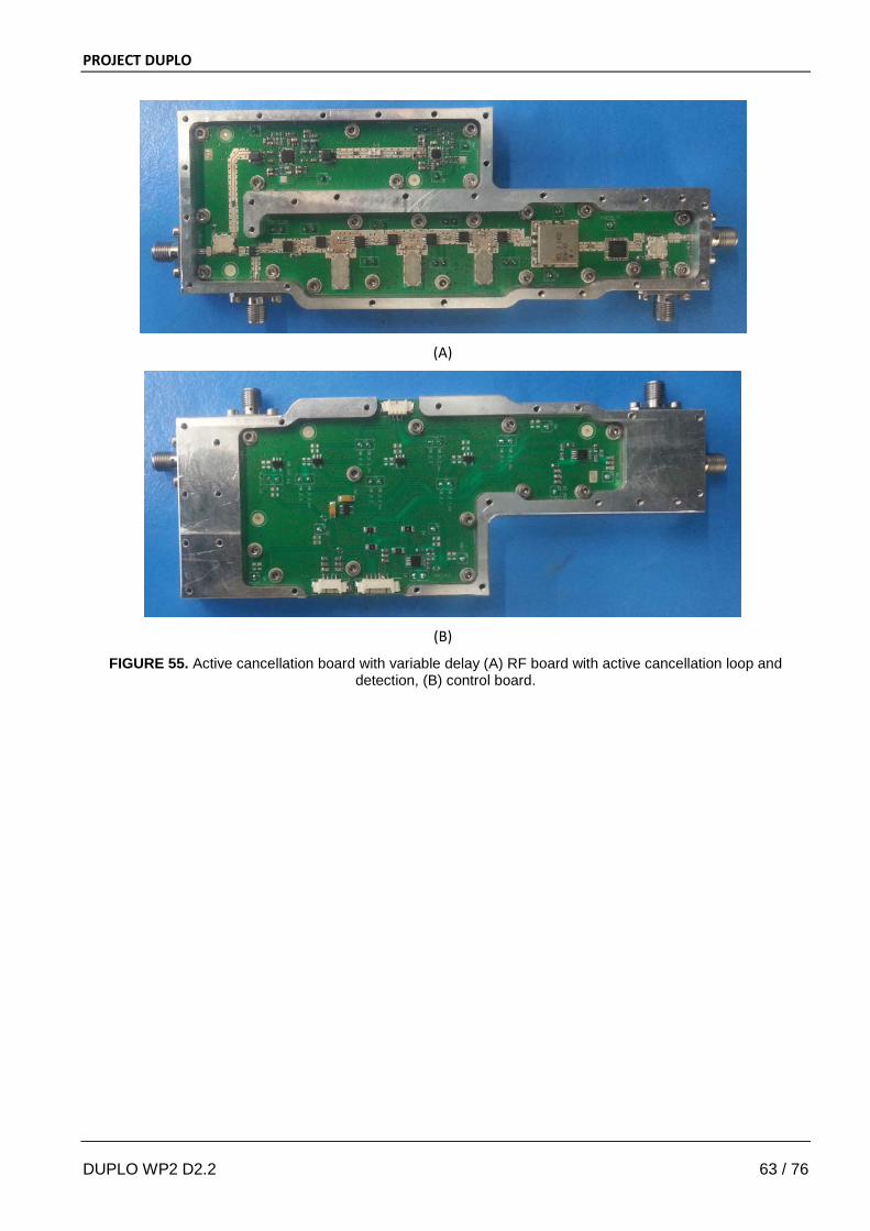
PROJECT DUPLO
(A)
(B)
FIGURE 55. Active cancellation board with variable delay (A) RF board with active cancellation loop and detection, (B) control board.
DUPLO WP2 D2.2 63 / 76
PROJECT DUPLO
5. INTEGRATION AND VALIDATION POTENTIAL
The DUPLO project sets a challenging goal of creating a “proof-of-concept” demonstrator, where several DUPLO solutions from different workpackages are integrated. To enable this integration, different design requirements have been defined in terms of validation platform, operation frequency, interconnections, test and validation signals and test case experiments [1, 12]. To ensure that the different solutions constructively contribute to the reduction of the self-interference, a strong collaboration between different workpackages has been established. Measurement results generated within WP2 (stand-alone and integrated in a prototyping platform) have been shared with WP3 to develop and verify their digital cancellation algorithms based on a realistic system conditions and RF isolation characteristics. This inter-workpackage collaboration comes in addition to the WP5 activities where the different solutions are integrated in the “proof-of-concept” demonstrator.
Different validation steps are being implemented towards the “proof-of-concept” demonstrator, and these steps increasingly integrate different solutions. The first validation step demonstrates the capabilities and performance of the individual WP2 solutions. The second validation step combines few individual solutions generated in WP2 or WP3. And finally , several DUPLO solutions will be integrated within WP5.
In WP2, several chip and antenna prototypes have been fabricated. As these prototypes might differ in functionality, some prototypes are better suited for integration in WP5 than others. In the next paragraphs, their suitability for integration with the other DUPLO solutions is described.
Two different antenna prototypes have been fabricated. Basically, both prototypes have the same functionality and the second prototype offers the best performance in terms of bandwidth. Therefore, the second prototype is currently introduced in the WP5 final integrated demonstrator, where the second active cancellation network will be integrated as described in this deliverable. The first active cancellation prototype was however intensively used in the past to develop the active cancellation concept, and measurements of its spectral characteristics have been shared with WP3. Additionally, the dual-polarized antenna is currently used to set-up a wireless link with another radio node which implements the EBD solution.
In the frame of the EBD activities, two prototypes have been fabricated. The first prototype implements a complete electrical balance duplexer which can interconnect a radio transceiver with a single port antenna. The second prototype implements only a balance network (no transformer) and was fabricated to investigate the shortcomings of the first prototype, namely the frequency tuning and the linearity of the balance network. Therefore, only the first prototype can be considered for integration with other DUPLO solutions. Based on this chip prototype, a validation platform has been constructed [6] which enabled to extensively measure the chip performance under realistic system conditions and to develop an efficient tuning algorithm. The chip characteristics measured with this platform have been shared with WP3. This platform has been extended towards a dual radio node setup with a full-duplex wireless link as depicted in FIGURE 56. Both radio nodes are currently equipped with an EBD as indicated by the green blocks. The measurements gained from this setup have been shared within DUPLO for further investigation and self-interference reduction. This setup will be extended by equipping one radio with a dual-polarized antenna solution from the DUPLO project and by including the digital cancellation algorithms from WP3. Note that this setup does not operate real-time; it performs off-line matlab calculations.
DUPLO WP2 D2.2 64 / 76
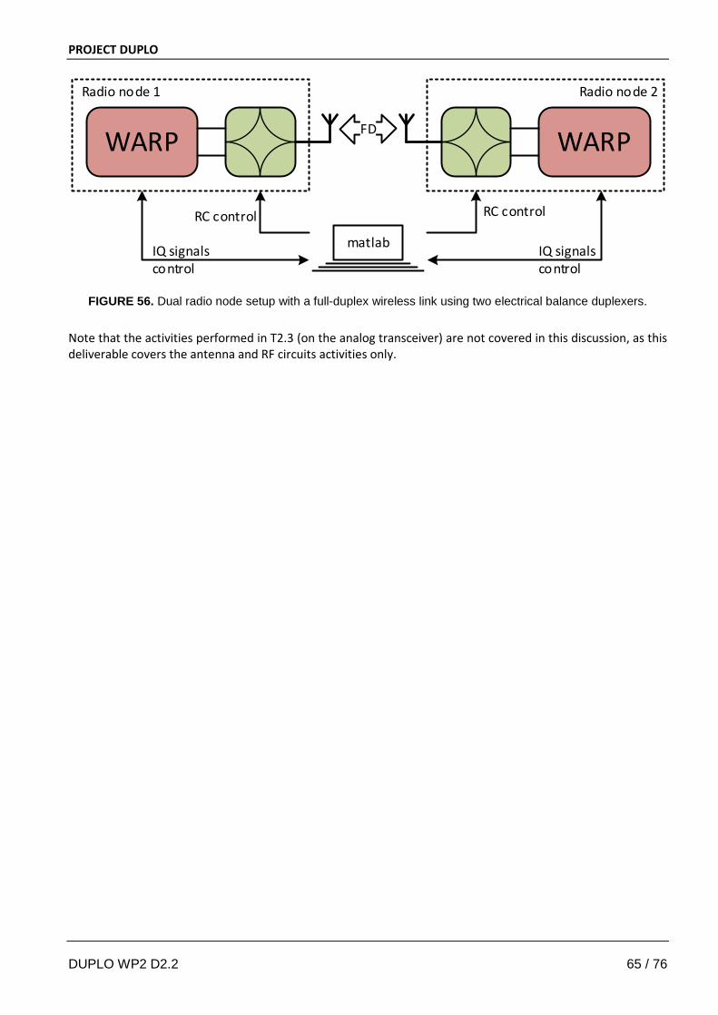
PROJECT DUPLO
WARP
Radio node 1
WARP
Radio node 2
matlab
RC control
IQ signalscontrol
FD
RC control
IQ signalscontrol
FIGURE 56. Dual radio node setup with a full-duplex wireless link using two electrical balance duplexers.
Note that the activities performed in T2.3 (on the analog transceiver) are not covered in this discussion, as this deliverable covers the antenna and RF circuits activities only.
DUPLO WP2 D2.2 65 / 76
PROJECT DUPLO
6. DISSEMINATION
The technical work performed in WP2 has gained substantial attention in the scientific community; all our publication submissions have been accepted and are being published. The peer-reviewed conferences and journals were carefully selected based on their scientific impact and relevance. Currently, apart from the contribution to DUPLO project-wide publications, the following WP2 work is being published:
IEEE Journal on Selected Areas in Communications (JSAC), Vol. 32, no. 9, September 2014.
The prestigious JSAC journal released a special on full-duplex communications. This issue publishes the main highlights and breakthrough innovations in the broad field of full-duplex communications. Our work on the radio hardware has been accepted and published:
B. Debaillie, D.J. van den Broek, C. Lavin, B. van Liempd, E.A.M. Klumperink, C. Palacios, J. Craninckx, B. Nauta, and A. Parssinen, “Analog/RF solutions enabling compact full-duplex radios,” IEEE Journal on Selected Areas in Communications (JSAC), vol. 32, no. 9, pp. 1662–1673, Sept. 2014.
This paper covers the work of all three WP2 tasks and discusses the radio system requirements, and presents novel hardware concepts and architectures developed within the DUPLO project.
9th International Conference on Cognitive Radio Oriented Wireless Networks (CrownCom), June 2–4, 2014, Oulu, Finland.
In combination with the CrownCom conference, the DUPLO project organized a workshop on full-duplex communications. This workshop offered an open call-for-papers, and the following paper has been accepted and published:
B. van Liempd, C. Lavin, S. Malotaux, D.J. van den Broek, B. Debaillie, C. Palacios, J.R. Long, E. Klumperink, and J. Craninckx, “RF self-interference cancellation for full-duplex,” International Conference on Cognitive Radio Oriented Wireless Networks (CrownCom), July 2014.
This paper describes the design and measurement results of the first antenna and electrical balance duplexer prototype. The performance of the antenna is enhanced by the active cancellation network developed in WP2. The reported self-interference suppression at RF equals more than 50dB for each solution and operates on the ISM band at 2.45GHz.
International Solid-State Circuits Conference (ISSCC), February 22-26, 2015, San Francisco, USA
ISSCC is the main solid state conference. The acceptance of our submissions is extremely valuable, and indicates that the solid state community is becoming more receptive for the circuit implementation of full-duplex wireless. The following papers have been accepted:
B. van Liempd, B. Hershberg, K. Raczkowski, S. Ariumi, U. Karthaus, K.F. Bink, J. Craninckx, “A >+70dBm IIP3 Single-Ended Electrical-Balance Duplexer in 0.18μm SOI CMOS,” in International Solid-State Circuits Conference (ISSCC), Feb. 2015.
J.D.A. van den Broek, E.A.M. Klumperink, and B. Nauta, “A Self-Interference Cancelling Receiver for In-Band Full-Duplex Wireless with Low Distortion under Cancellation of Strong TX leakage,’ in International Solid-State Circuits Conference (ISSCC), Feb. 2015.
DUPLO WP2 D2.2 66 / 76

PROJECT DUPLO The first paper builds further on the EBD concepts developed within DUPLO in SOI technology. The second paper describes the work performed in the third task on the transceiver circuit.
1st International Conference on 5G for Ubiquitous Connectivity (5GU), November 26–28, 2014, Levi, Finland
The 5GU conference is particularly interesting for our work, as we believe that full-duplex is a valuable technique within the next mobile communications generation (5G). Therefore we are happy that our submitted paper has been accepted and will be published:
M. Mikhael, B. van Liempd, J. Craninckx, R. Guindi, and B. Debaillie, “A full-duplex transceiver prototype with in-system automated tuning of the RF self-interference cancellation,” in IEEE International Conference on 5G for Ubiquitous Connectivity, Nov. 2014.
This paper describes a full-duplex transceiver prototype platform comprising the electrical balance duplexer and WARPv3, and proposes an intelligent EBD tuning algorithm. This work is mainly considered as WP5 activities, but uses the hardware results generated in WP2.
DUPLO WP2 D2.2 67 / 76
PROJECT DUPLO
7. STATE-OF-THE-ART AND FUTURE OPPORTUNITIES
Full-duplex has gained a lot of attention over the last couple of years. This attention has been accelerated because novel and interesting techniques are being developed which attempt to solve one of the main problems of full-duplex communications: the self-interference in the radio nodes. Apart from the DUPLO project, also other research groups are proposing new techniques to reduce the self-interference. The most promising techniques come from research groups which consider a system approach where the self-interference is rejected and cancelled at different locations in the radio, i.e. at the antenna and in the RF and digital domain. During the DUPLO project, WP2 carefully tracked the activities of other research groups in order to stay ahead and to differentiate in terms of objectives and technical solutions.
The main objective of WP2 was to develop solutions which are commercially attractive in terms of form-factor, system integration, process technology and operation flexibility. Each of these objectives are, however, contradicting with the self-interference problem which is easier to resolve with large form factor devices, circuits and antenna structures. Therefore, state-of-the-art solutions from other research institutes might present better self-interference rejection/cancellation values, but they cannot be scaled towards the compact portable applications WP2 is targeting. The WP2 objective might trade-in some self-interference rejection/cancellation performance, but we are leading the research to create small form-factor transceiver system solutions which can be integrated in commercially attractive compact radio devices, while offering attractive self-interference values.
In beginning of the DUPLO project, the selection of the antenna and RF-circuit techniques has been deeply investigated [4, 1, 3] for application in compact full-duplex radios. As the antenna and RF-circuit activities are now finalized within the DUPLO project, and as they are being integrated with the solutions from other workpackages, it is interesting to reflect on the advances of other research groups on similar techniques, and to discuss the future opportunities of the current WP2 solutions. These future opportunities can be resolved in future work after the DUPLO project. This will be discussed in the next sections, where first the dual polarized antenna architecture will be discussed in combination with the active antenna, and then, the electrical balance duplexer will be discussed.
7.1. Dual-port FD antenna systems TABLE 10 shows the survey of recent literature on antenna and analog self-interference cancellation techniques. As can be seen from listed references, most of the proposed antenna cancellation techniques operate with at least two antennas, having one antenna for reception and one antenna for transmission. Implementing separate TX and RX antennas provides a high level of passive SI suppression, however this technique is not scalable to compact form-factor devices. Additionally, multi-antenna architectures moves the duplexing problem to spatial domain due to the presence of multiple radiating elements degrades the radiation properties of the antennas, creating sometimes null-zones in the far-field region, as deliverable D2.1 describes [1]. As already mentioned, DUPLO project focuses on the research of new antenna SI suppression techniques implementable in commercially attractive compact form-factor devices. Due to this reason, multi-antenna approaches must be replaced by other antenna structures which allows for an efficient integration in compact radio devices. As previously described in this deliverable, the antenna solution proposed in DUPLO project relies on the use of orthogonal polarizations to achieve enough isolation between TX and RX. This SI suppression techniques is implementable on a single radiating aperture by means of using a two-port antenna. Therefore, the proposed technique allows for an easy integration in compact devices and moreover it avoids the spatial domain problem, causing no degradation in the far-field coverage.
As illustrated in TABLE 10, the use of single antenna solutions has also been explored in [29], [30] and [31]. In particular, [29] and [31] make use of a commercial dipole (single-port antenna) combined with an RF circulator to achieve isolation between TX and RX. Nevertheless, circulators are typically bulky components at
DUPLO WP2 D2.2 68 / 76
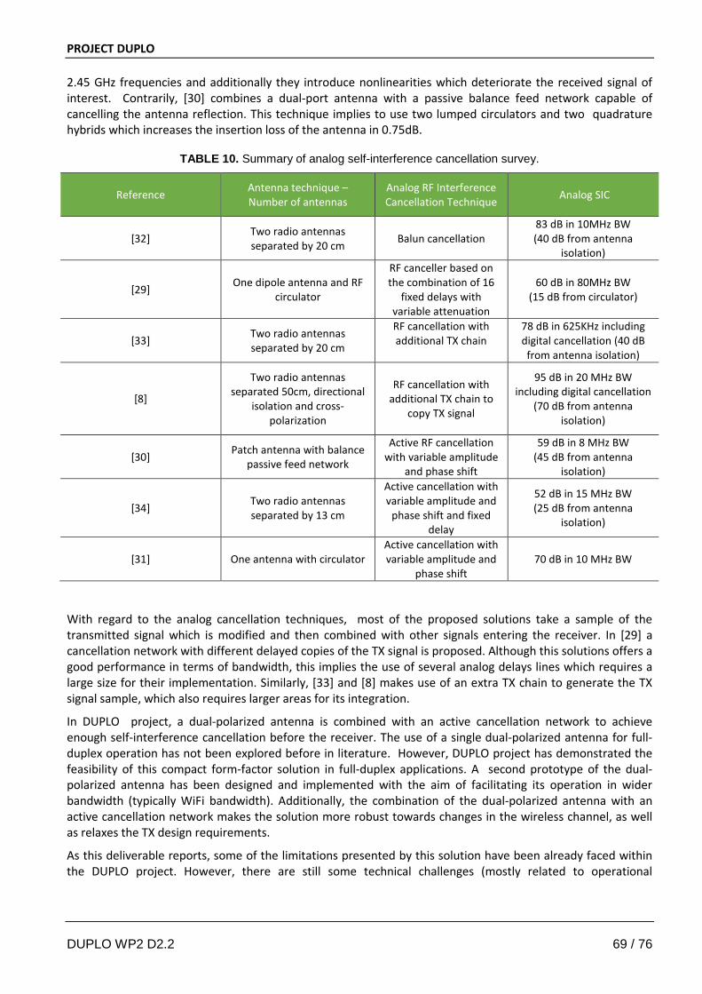
PROJECT DUPLO 2.45 GHz frequencies and additionally they introduce nonlinearities which deteriorate the received signal of interest. Contrarily, [30] combines a dual-port antenna with a passive balance feed network capable of cancelling the antenna reflection. This technique implies to use two lumped circulators and two quadrature hybrids which increases the insertion loss of the antenna in 0.75dB.
TABLE 10. Summary of analog self-interference cancellation survey.
Reference Antenna technique – Number of antennas
Analog RF Interference Cancellation Technique Analog SIC
[32] Two radio antennas separated by 20 cm Balun cancellation
83 dB in 10MHz BW (40 dB from antenna
isolation)
[29] One dipole antenna and RF circulator
RF canceller based on the combination of 16
fixed delays with variable attenuation
60 dB in 80MHz BW (15 dB from circulator)
[33] Two radio antennas separated by 20 cm
RF cancellation with additional TX chain
78 dB in 625KHz including digital cancellation (40 dB from antenna isolation)
[8]
Two radio antennas separated 50cm, directional
isolation and cross-polarization
RF cancellation with additional TX chain to
copy TX signal
95 dB in 20 MHz BW including digital cancellation
(70 dB from antenna isolation)
[30] Patch antenna with balance passive feed network
Active RF cancellation with variable amplitude
and phase shift
59 dB in 8 MHz BW (45 dB from antenna
isolation)
[34] Two radio antennas separated by 13 cm
Active cancellation with variable amplitude and
phase shift and fixed delay
52 dB in 15 MHz BW (25 dB from antenna
isolation)
[31] One antenna with circulator Active cancellation with variable amplitude and
phase shift 70 dB in 10 MHz BW
With regard to the analog cancellation techniques, most of the proposed solutions take a sample of the transmitted signal which is modified and then combined with other signals entering the receiver. In [29] a cancellation network with different delayed copies of the TX signal is proposed. Although this solutions offers a good performance in terms of bandwidth, this implies the use of several analog delays lines which requires a large size for their implementation. Similarly, [33] and [8] makes use of an extra TX chain to generate the TX signal sample, which also requires larger areas for its integration.
In DUPLO project, a dual-polarized antenna is combined with an active cancellation network to achieve enough self-interference cancellation before the receiver. The use of a single dual-polarized antenna for full-duplex operation has not been explored before in literature. However, DUPLO project has demonstrated the feasibility of this compact form-factor solution in full-duplex applications. A second prototype of the dual-polarized antenna has been designed and implemented with the aim of facilitating its operation in wider bandwidth (typically WiFi bandwidth). Additionally, the combination of the dual-polarized antenna with an active cancellation network makes the solution more robust towards changes in the wireless channel, as well as relaxes the TX design requirements.
As this deliverable reports, some of the limitations presented by this solution have been already faced within the DUPLO project. However, there are still some technical challenges (mostly related to operational
DUPLO WP2 D2.2 69 / 76
PROJECT DUPLO bandwidth) which could be tackled in the future, as for instance to further investigate the application of any antenna miniaturization technique (e.g. to use dielectric materials with higher dielectric constants) which provides high isolation in a wider bandwidth (normally antenna miniaturization techniques provide very limited bandwidth), or to explore different analog cancellation architectures which offers wider bandwidth operation maintaining a compact integration area (namely how to implement analog delay lines in a reduced size). These are some of the ideas that could be considered to further improve the performance of this solution.
7.2. Electrical balance duplexer Only few publications consider novel RF duplexer solutions in FD applications. Most research groups focus on antenna solutions in combination with active cancellation in RF, baseband or mixed. The few publications which use an convention single-port antenna mainly use a circulator to isolate the received signal from the transmitted signal. Such circulators are typically bulky components which are not flexible in operation. Therefore, these designs target different objectives and is not considered to benchmark with our EBD work.
In the JSAC edition on full-duplex communications, apart from our WP2 publication, another paper was published by Laughlin et al. [35], in which the concept of electrical-balance duplexing is also proposed for in-band FD. Their paper investigates practical variation of antennas in different environmental scenarios and shows simulation results using their antenna measurements, without reporting any FD designs or design considerations.
Interestingly, another paper written by Lu et al. [36] demonstrates a prototype where the EBD concept is applied at millimeter-wave frequencies. This design targets mainly radar applications, where the incident reflected wave has shifted polarisation compared to the transmitted signal. Two antennas are then balanced to achieve a low-loss implementation. Unfortunately, this prototype was not demonstrated with actual antennas, but with 50 Ohm terminations (instrumentation equipment) instead.
In FDD applications, the EBD concept is considered more often. Although the difference in application and specification between FDD and FD, these design activities are monitored carefully to enable synergy. The current best reference is presented in the DUPLO ISSCC submission [19], where an state-of-the-art overview is given in TABLE 11. This overview indicates that the performances for the chip based on the DUPLO concepts exceeds the competition, especially in terms of IIP3 (linearity) and Rx insertion loss. Much of this performance is gained by the SOI technology, which in its turn leads to a larger area footprint, but this area remains acceptably small (1.75 mm2).
DUPLO WP2 D2.2 70 / 76
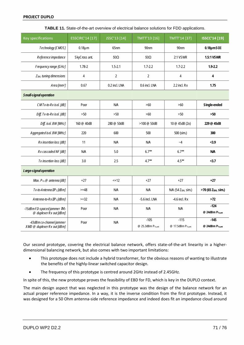
PROJECT DUPLO
TABLE 11. State-of-the-art overview of electrical balance solutions for FDD applications.
Key specifications ESSCIRC’14 [17] JSSC’13 [14] TMTT’13 [16] TMTT’14 [37] ISSCC’14 [19]
Technology [CMOS] 0.18µm 65nm 90nm 90nm 0.18µm SOI
Reference impedance SkyCross ant. 50Ω 50Ω 2:1 VSWR 1.5:1 VSWR
Frequency range [GHz] 1.78-2 1.5-2.1 1.7-2.2 1.7-2.2 1.9-2.2
ZBAL tuning dimensions 4 2 2 4 4
Area [mm2] 0.67 0.2 incl. LNA 0.6 incl. LNA 2.2 incl. Rx 1.75
Small-signal operation
CM Tx-to-Rx isol. [dB] Poor N/A >60 >60 Single-ended
Diff. Tx-to-Rx isol. [dB] >50 >50 >60 >50 >50
Diff. isol. BW [MHz] 160 @ 40dB 280 @ 50dB >100 @ 50dB 10 @ 45dB (2x) 229 @ 45dB
Aggregated isol. BW [MHz] 220 600 500 500 (sim.) 300
Rx insertion loss [dB] 11 N/A N/A ~4 <3.9
Rx cascaded NF [dB] N/A 5.0 6.7** 6.7** N/A
Tx insertion loss [dB] 3.0 2.5 4.7** 4.5** <3.7
Large-signal operation
Max. PTx @ antenna [dB] +27 <+12 +27 +27 +27
Tx-to-Antenna IIP3 [dBm] >+48 N/A N/A N/A (54 ZBAL sim.) >70 (65 ZBAL sim.)
Antenna-to-Rx IIP3 [dBm] >+32 N/A -5.6 incl. LNA -4.6 incl. Rx >72
-15dBm FD-spaced jammer IM3
@ duplexer Rx out [dBm] Poor N/A N/A N/A
-124 @ 24dBm PTx,ant
-43dBm co-channel jammer XMD @ duplexer Rx out [dBm]
Poor N/A -105 @ 25.3dBm PTx,ant
-115 @ 17.5dBm PTx,ant
-145 @ 24dBm PTx,ant
Our second prototype, covering the electrical balance network, offers state-of-the-art linearity in a higher-dimensional balancing network, but also comes with two important limitations:
• This prototype does not include a hybrid transformer, for the obvious reasons of wanting to illustrate the benefits of the highly-linear switched capacitor design.
• The frequency of this prototype is centred around 2GHz instead of 2.45GHz.
In spite of this, the new prototype proves the feasibility of EBD for FD, which is key in the DUPLO context.
The main design aspect that was neglected in this prototype was the design of the balance network for an actual proper reference impedance. In a way, it is the inverse condition from the first prototype. Instead, it was designed for a 50 Ohm antenna-side reference impedance and indeed does fit an impedance cloud around
DUPLO WP2 D2.2 71 / 76
PROJECT DUPLO 50 Ohm. As such, in future work, the balance network impedance still needs attention. There are several dimensions to that problem:
• How can we design a balance network that can (ideally) curve-fit across frequency the impedance of a generic antenna impedance?
• What does that generic antenna impedance (across frequency) actually look like?
• How to design an antenna for this specific application, with limited impedance variation across frequency and environmental condition?
• How to do the tuning of such a (probably) complex balance-network impedance? Likely this is not trivial, with multiple optima for a single impedance at a single frequency, and even across a larger bandwidth.
• How to do the sensing of the quality of operation of the duplexer (i.e. the isolation)? Impedance sensing, temperature sensing, signal swing sensing, all kinds of sensors are likely to be required to make a practical implementation.
These challenges should be tackled in future research.
These challenges, in combination of the opportunities generated in the field of FDD, illustrate the room for growth and improvement that still exists in this type of duplexers.
Given the antenna and RF circuit techniques described in this document, other than compact and portable radio types could be considered. An interesting field of application is for example multi-antenna (MIMO) radio systems, where all antennas are operating on the same frequency at the same time. One could think to simply replicate the antenna/RF full-duplex techniques over the different antenna path. This approach will however fail because cross-talk between the different antennas will cause severe ‘self’-interference on each receiver. Cancelling this interference is much more complex that in the SISO case as described in this document, because the ‘self’-interferences are subjected to different cross-talk paths, and this cross-talk depends on the instantaneous reflecting environment and might be subjected to different and relatively large time delays. Therefore the interference between the antennas is extremely difficult to quantify and compensate, especially at antenna or RF circuit level. Although the MIMO-FD concept is already described at network level, practical and functional antenna/RF solutions are currently not existing. Potentially, an integrated multi-antenna system could be build which minimizes inter-antenna cross-talk and/or RF cancellation circuits can be severely equipped with digital processing to quantify the different cross-talk paths. Alternative methods are to apply beamforming to direct the antenna radiation and/or operate on millimeter-wave frequencies where the propagation distances are smaller. Based on the pervious description, the design of a functional MIMO-FD radio remains a challenging research topic.
DUPLO WP2 D2.2 72 / 76
PROJECT DUPLO
8. SUMMARY AND CONCLUSIONS
This document presents the second and final phase of the design and implementation of the prosed antenna and RF circuit solutions, enabling compact full-duplex wireless radio devices. This document evaluates the results achieved during the first phase, which are reported in D2.1 [1] and in the JSAC publication [3] and develops, designs and fabricates new prototypes to improve the performance or to investigate the elimination of potential show-stoppers.
The key design requirements in both phases are to minimize the RF self-interference and to target small form-factor antenna/RF solutions which can be implementable in compact radio devices. These requirements are however contradictory as dense integration and compact form-factor designs reduces the physical spacing between the transmitting and receiving elements/circuits/signals. In state-of-the-art full-duplex radio system design, this physical spacing is generally exploited to increase the self-interference isolation.
The presented techniques focus on antenna and RF circuit techniques only, and in combination with transceiver and digital cancellation techniques, an overall self-inference rejection of about 100dB is targeted for a mid-end scenario as described in D1.1 [4]. Based on the link budget calculation over realistic scenarios presented in D2.3.1 [2] and [3], the RF self-interference isolation factor should exceed 45 a 50dB over a bandwidth of 10MHz.
This document continues on the three designs presented in D2.1 [D2.1, JSAC] covering a dual-polarized microstrip patch antenna design, and tunable electrical balance duplexer design and an active cancellation network design to be applied at RF. This document describes how the performance of the designs can be improved, and validates these improvements based on the fabrication and measurements of new prototypes.
A second dual-polarized microstrip patch antenna prototype has been designed, fabricated and measured. This prototype builds on similar topology as the first prototype and offers the same functionalities, but provides better performance (e.g. bandwidth) and is smaller in size. A parametric optimization methodology has been developed to derive the design parameters of the second antenna prototype. The second prototype is smaller (60x60x8mm) and offers wider bandwidth capabilities with an SI isolation of 49dB over 10MHz and 42dB over 80MHz. Over 10MHz, antenna gain is higher than 6.5dB and offers a 3dB beamwidth of more than 70 degrees with an antenna efficiency of more than 75%. The isolation characteristics and robustness can be improved together with the active cancellation described in this document. This antenna prototype is used for integration in the DUPLO proof-of-concept demonstrator.
Measurements in the electrical balance duplexer (EBD) first prototype indicated two main issues potentially hampering the exploitation for full-duplex operation. These issues are the limited bandwidth and the limited linearity of the balance network. These issues are described in this document and a second prototype has been design and fabricated to investigate the capability to resolve these specific issues. To avoid the complexity overhead, this second prototype includes a tunable balance network only, without the transformer. This second prototype is implemented in SOI technology to leverage the linearity, and an additional degrees of tunability has been implemented in the balance network to trade-off the average SI isolation with the isolation bandwidth. The second prototype has been implemented in 0.18um SOI CMOS technology and covers an area of 0.9mm2 only. This design offers an extremely high linearity (IIP3 > 70dBm) and can handle relatively high transmission power (e.g. 27dBm) without considerable heating-up.
The work on the active cancellation, initiated in D2.1 [1] has been continued and extended. This document details the design and component selection of the cancellation network and presents an automatic tuning method to control and tune the network to its optimal configuration in an efficient way. The active cancellation method has been verified based on measurements in combination with the dual-polarized antenna described in this document. These measurements indicate an SI reduction of 15dB in addition to the isolation provided by the antenna solution. Additionally, the potential benefits of including a variable delay line in the active cancellation network is introduced in this document, and will be further addressed in WP5.
DUPLO WP2 D2.2 73 / 76
PROJECT DUPLO As suggested in the previous description, WP2 actively shares its gained results with the DUPLO project. The second antenna prototype together with the active cancellation and the first EBD prototype will be integrated in the proof-of-concept demonstrator of WP5, and specific stand-alone measurement results are shared e.g. with WP3 to verify and optimize the digital cancellation algorithms. This cross-workpackage collaboration is described in chapter 5.
The presented designs can be further investigated and optimized within our outside of this DUPLO project. Within the DUPLO project, the tuning method and algorithm will be further developed and optimized both for the EBD and the active cancellation network. Also, the active cancellation network design in combination with the dual-polarized antenna will be validated further and improved if required. Outside the DUPLO project, the second electrical balance network prototype will be integrated with a transformer to create a functional duplexer, and more investigation will be performed on how to efficiency tune the multiple tuning knobs and to model the antenna impedance behaviour over frequency and operation conditions. This is described more in detail in chapter 7.
The presented work mainly differentiates with state-of-the-art in terms of form factor and integration potential in compact or portable radio system devices. In this document, the developed techniques are compared with state-of-the-art solutions which apply similar techniques or topologies. With respect to the antenna structure, the usage of orthogonal polarization with a single antenna element is hardly described in literature for full-duplex application, although it enables to create small form-factor antennas. To increase its SI isolation robustness against the effects of nearby objects, we developed the active cancellation network. With respect to the duplexer, electrical balancing designs for full-duplex are hardly described in literature. In FDD applications, the EB architecture is more frequency considered, but still our design outperforms the performances presented in literature. The designs presented in this document well received by the scientific community as this work has been accepted for publication in several peer-reviewed IEEE conferences as described in chapter 6, and the comparison with state-of-the-art is given in chapter 7.
DUPLO WP2 D2.2 74 / 76
PROJECT DUPLO
9. REFERENCES
[1] B. Debaillie, “Design and measurement report on RF and antenna solutions for self-interference cancellation,” in INFSO-ICT- 316369 DUPLO - Report D2.1, April 2014.
[2] D.J. van den Broek, “Transceiver circuits simulation, implementation and measurement report,” in INFSO-ICT- 316369 DUPLO - Report D2.3.1, April 2014.
[3] B. Debaillie, D.J. van den Broek, C. Lavin, B. van Liempd, E.A.M. Klumperink, C. Palacios, J. Craninckx, B. Nauta, and A. Parssinen, “Analog/RF solutions enabling compact full-duplex radios,” IEEE Journal on Selected Areas in Communications (JSAC), vol. 32, no. 9, pp. 1662–1673, Sept. 2014.
[4] V. Tapio, “System scenarios and technical requirements for full-duplex concept,” in INFSO-ICT- 316369 DUPLO - Report D1.1, April 2013.
[5] B. van Liempd, C. Lavin, S. Malotaux, D.J. van den Broek, B. Debaillie, C. Palacios, J.R. Long, E. Klumperink, and J. Craninckx, “RF self-interference cancellation for full-duplex,” International Conference on Cognitive Radio Oriented Wireless Networks (CrownCom), July 2014.
[6] M. Mikhael, B. van Liempd, J. Craninckx, R. Guindi, and B. Debaillie, “A full-duplex transceiver prototype with in-system automated tuning of the RF self-interference cancellation,” in IEEE International Conference on 5G for Ubiquitous Connectivity, Nov. 2014.
[7] M. Duarte and A. Sabharwal, “Full-duplex wireless communications using off-the-shelf radios: Feasibility and first results,” in Asilomar Conference on Signals, Systems and Computers (ASILOMAR), pp. 1558–1562, Nov. 2010.
[8] E. Everett, A. Sahai, and A. Sabharwal, “Passive self-interference suppression for full-duplex infrastructure nodes,” IEEE Transactions on Wireless Communications, vol. 13, no. 2, pp. 680–694, Feb. 2014.
[9] A. Sahai, G. Patel, and Sabharwal A., “Pushing the limits of full-duplex: Design and real-time implementation,” Rice University Technical Report, 2011.
[10] A.K. Khandani, “Methods for spatial multiplexing of wireless two-way channels,” US Patent, 2010. [11] J.I. Choi, M. Jain, K. Srinivasan, P. Levis, and S. Katti, “Achieving single channel, full duplex wireless
communication,” in International Conference on Mobile Computing and Networking, 2010. [12] C. Palacios, “Early integration and test,” in INFSO-ICT- 316369 DUPLO - Report D5.1, June 2014. [13] N.M. Gould, D. Orban, A. Sartenaer, and P.L. Toint, “Sensitivity of trust-region algorithms to their
parameters,” 4OR, vol. 3, no. 3, pp. 227–241, 2005. [14] M. Mikhemar, H. Darabi, and A.A. Abidi, “A multiband RF antenna duplexer on CMOS: Design and
performance,” IEEE Journal of Solid-State Circuits, vol. 48, no. 9, pp. 2067–2077, Sept. 2013. [15] S.H. Abdelhalem, P.S. Gudem, and L.E. Larson, “Hybrid transformer-based tunable integrated duplexer
with antenna impedance tracking loop,” in IEEE Custom Integrated Circuits Conference (CICC), Sept. 2013.
[16] S.H Abdelhalem, P.S. Gudem, and L.E. Larson, “Hybrid transformer-based tunable differential duplexer in a 90-nm CMOS process,” IEEE Transactions on Microwave Theory and Techniques, March 2013.
[17] B van Liempd, R. Singh, S. Malotaux, P. Reynaert, J. R. Long, and J. Craninckx, “A dual-notch +27dBm Tx-power electrical-balance duplexer,” in IEEE European Solid-State Circuits Conference (ESSCIRC), Sept. 2014.
[18] W. Dawn, R. Wolf, A. Joseph, A. Botula, P. Rabbeni, M. Boenke, D. Harame, and J. Dunn, “High performance SOI RF switches for wireless applications,” in IEEE International Conference on Solid-State and Integrated Circuit Technology (ICSICT), pp. 611–614, Nov. 2010.
[19] B. van Liempd, B. Hershberg, K. Raczkowski, S. Ariumi, U. Karthaus, K.F. Bink, and Craninckx J., “A >+70dBm IIP3 single-ended electrical-balance duplexer in 0.18um SOI CMOS,” in International Solid-State Circuits Conference (ISSCC), Feb. 2015.
[20] Anaren, “20 dB directional coupler,” 1P620S, 2014. [21] Hittite, “450 degrees analog phase shifter, 2-4GHz,” HMC928LP5, 2014. [22] Minicircuits, “Voltage variable attenuator,” RVA-33, 2014.
DUPLO WP2 D2.2 75 / 76
PROJECT DUPLO [23] Minicircuits, “Power combiner,” SP-2U2, 2014. [24] Skyworks, “GaAs ic high-isolation positive control SPDT nonreflective switch LF–4 Ghz,” AS186, 2014. [25] Anaren, “10dB directional coupler,” 1P610S, 2014. [26] Analog Devices, “60 dB gain control range,” ADL5330, 2014. [27] Analog Devices, “Logarithmic detector/controller,” ADL5513, 2014. [28] Anaren, “Delay line,” XDL15-2-020S, 2014. [29] D. Bharadia, E. McMilin, and S. Katti, “Full duplex radios,” in ACM Special Interest Group on Data
Communications, 2013. [30] M.E. Knox, “Single antenna full duplex communications using a common carrier,” in IEEE Wireless and
Microwave Technology Conference (WAMICON), April 2012. [31] N. Phungamngern, P. Uthansakul, and M. Uthansakul, “Digital and RF interference cancellation for
single-channel full-duplex transceiver using a single antenna,” in International Conference on Electrical Engineering/Electronics, Computer, Telecommunications and Information Technology (ECTI-CON), pp. 1–5, May 2013.
[32] M. Jain, J.I. Choi, T. Kim, D. Bharadia, S. Seth, K. Srinivasan, P. Levis, S. Katti, and P. Sinha, “Practical, real-time, full duplex wireless,” in International Conference on Mobile Computing and Networking, 2011.
[33] M. Duarte, C. Dick, and A. Sabharwal, “Experiment-driven characterization of full-duplex wireless systems,” IEEE Transactions on Wireless Communications, vol. 11, no. 12, pp. 4296–4307, Dec. 2012.
[34] Y. Binqi, D. Yunyang, Y. Zhiqiang, and Z. Jianyi, “An RF self-interference cancellation circuit for the full-duplex wireless communications,” in International Symposium on Antennas Propagation (ISAP), vol. 02, pp. 1048–1051, Oct. 2013.
[35] L. Laughlin, M.A. Beach, K.A. Morris, and J.L. Haine, “Optimum single antenna full duplex using hybrid junctions,” IEEE Journal on Selected Areas in Communications (JSAC), vol. 32, no. 9, pp. 1653–1661, Sept. 2014.
[36] C. Lu, M.K. Matters-Kammerer, R. Mahmoudi, and P.G.M. Baltus, “A millimeter-wave tunable transformer-based dual-antenna duplexer with 50dB isolation,” in IEEE Custom Integrated Circuits Conference (CICC), Sept. 2014.
[37] S.H. Abdelhalem, P.S. Gudem, and L.E. Larson, “Tunable cmos integrated duplexer with antenna impedance tracking and high isolation in the transmit and receive bands,” IEEE Transactions on Microwave Theory and Techniques (TMTT),, vol. 62, no. 9, pp. 2092–2104, Sept 2014.
DUPLO WP2 D2.2 76 / 76