Embed Size (px)
DESCRIPTION
DTMF ROBO
Citation preview

DTMF BASED WIRELESS ROBOT
SUBMITTED BY
INTRODUCTION
DTMF Mobile ROBO is a machine that can be controlled with a
mobile . In this project, the robot is controlled by a mobile
phone that makes a call to the mobile phone attached to the
robot. In the course of a call, if any button is pressed, a tone
corresponding to the button pressed is heard at the other end of
the call. This tone is called "Dual Tone Multiple-Frequency"
(DTMF) tone. The robot perceives this DTMF tone with the
help of the phone stacked on the robot. The received tone is
processed by the microcontroller with the help of DTMF
decoder. The microcontroller then transmits the signal to the
motor driver ICs to operate the motors & our robot starts
moving
Conventionally, Wireless-controlled robots use rf circuits, which
have the drawbacks of limited working range, limited frequency
range and the limited control. Use of a mobile phone for robotic
control can overcome these limitations. It provides the
advantage of robust control, working range as large as the
coverage area of the service provider, no interference with other

controllers and up to twelve controls.
Although the appearance and the capabilities of robots vary
vastly, all robots share the feature of a mechanical, movable
structure under some form of control. The Control of robot
involves three distinct phases: perception, processing and action.
Generally, the preceptors are sensors mounted on the robot ,
processing is done by the on-board microcontroller or processor,
and the task is performed using motors or with some other
actuators.
In this project the robot, is controlled by a mobile phone that
makes call to the mobile phone attached to the robot in the
course of the call, if any button is pressed control corresponding
to the button pressed is heard at the other end of the call. This
tone is called dual tone multi frequency tome (DTMF) robot
receives this DTMF tone with the help of phone stacked in the
robot
The received tone is processed by the atmega16 microcontroller
with the help of DTMF decoder MT8870 the decoder decodes
the DTMF tone in to its equivalent binary digit and this binary
number is send to the microcontroller, the microcontroller is
preprogrammed to take a decision for any give input and outputs
its decision to motor drivers in order to drive the motors for
forward or backward motion or a turn.
The mobile that makes a call to the mobile phone stacked in the
robot acts as a remote. So this simple robotic project does not
require the construction of receiver and transmitter units.
DTMF signaling is used for telephone signaling over the line in
the voice frequency band to the call switching center. The
version of DTMF used for telephone dialing is known as touch
tone.
DTMF assigns a specific frequency (consisting of two separate
tones) to each key s that it can easily be identified by the
electronic circuit. The signal generated by the DTMF encoder is
the direct algebraic submission, in real time of the amplitudes of
two sine (cosine) waves of different frequencies, i.e., pressing 5
will send a tone made by adding 1336 Hz and 770 Hz to the
other end of the mobile. The important components of this robot
are DTMF decoder, Microcontroller and motor driver.
An MT8870 series DTMF decoder is used here. All types of the
mt8870 series use digital counting techniques to detect and
decode all the sixteen DTMF tone pairs in to a four bit code
output. The built -in dial tone rejection circuit eliminated the

need for pre- filtering. When the input signal given at pin2 (IN-)
single ended input configuration is recognized to be effective,
the correct four bit decode signal of the DTMF tone is
transferred to Q1 (pin11) through Q4(pin14) outputs.

BLOCK DIAGRAM
L293D
POWER SUPPLY
TELEPHONE
DTMF
DECODER
MOTOR
8051
MICROCONTR
OLLER
MOTOR
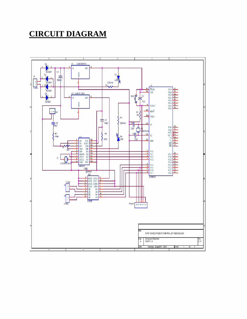
CIRCUIT DIAGRAM

COMPONENT LIST
Sr. no Equipment Quantity
1 IC 8051 MC 1
2 MT 8870 DTMF IC 1
3 Crystal (3.579545mhz) 1
4 VOLTAGE REGULATOR 1
5 2 LINE LCD DISPLAY 1
6 CRYSTAL
OSCILLATOR(11.0592mhz)
1
7 DIODE 1
8 PUSH BUTTON 1
9 LEDS 4
10 RESISTER(220Ω,4.7kΩ,10kΩ) BOX
11 CAPACITORS(10uf,1000uf) 5
12 MOTORS 2
13 L293D 1

A BRIEF INTRODUCTION TO 8051
MICROCONTROLLER:
When we have to learn about a new computer we have to
familiarize about the machine capability we are using, and we
can do it by studying the internal hardware design (devices
architecture), and also to know about the size, number and the
size of the registers.
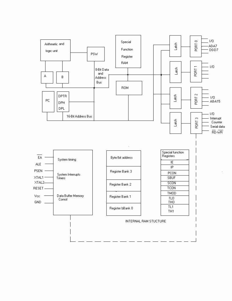
A microcontroller is a single chip that contains the
processor (the CPU), non-volatile memory for the program
(ROM or flash), volatile memory for input and output (RAM), a
clock and an I/O control unit. Also called a "computer on a
chip," billions of microcontroller units (MCUs) are embedded
each year in a myriad of products from toys to appliances to
automobiles. For example, a single vehicle can use 70 or more
microcontrollers. The following picture describes a general
block diagram of microcontroller.
AT89S52: The AT89S52 is a low-power, high-performance
CMOS 8-bit microcontroller with 8K bytes of in-system

programmable Flash memory. The device is manufactured using
Atmel’s high-density nonvolatile memory technology and is
compatible with the industry-standard 80C51 instruction set and
pin out. The on-chip Flash allows the program memory to be
reprogrammed in-system or by a conventional nonvolatile
memory programmer. By combining a versatile 8-bit CPU with
in-system programmable Flash on a monolithic chip, the Atmel
AT89S52 is a powerful microcontroller, which provides a highly
flexible and cost-effective solution to many, embedded control
applications. The AT89S52 provides the following standard
features: 8K bytes of Flash, 256 bytes of RAM, 32 I/O lines,
Watchdog timer, two data pointers, three 16-bit timer/counters, a
six-vector two-level interrupt architecture, a full duplex serial
port, on-chip oscillator, and clock circuitry. In addition, the
AT89S52 is designed with static logic for operation down to
zero frequency and supports two software selectable power
saving modes. The Idle Mode stops the CPU while allowing the
RAM, timer/counters, serial port, and interrupt system to
continue functioning. The Power-down mode saves the RAM
con-tents but freezes the oscillator, disabling all other chip
functions until the next interrupt.

The hardware is driven by a set of program instructions, or
software. Once familiar with hardware and software, the user
can then apply the microcontroller to the problems easily.
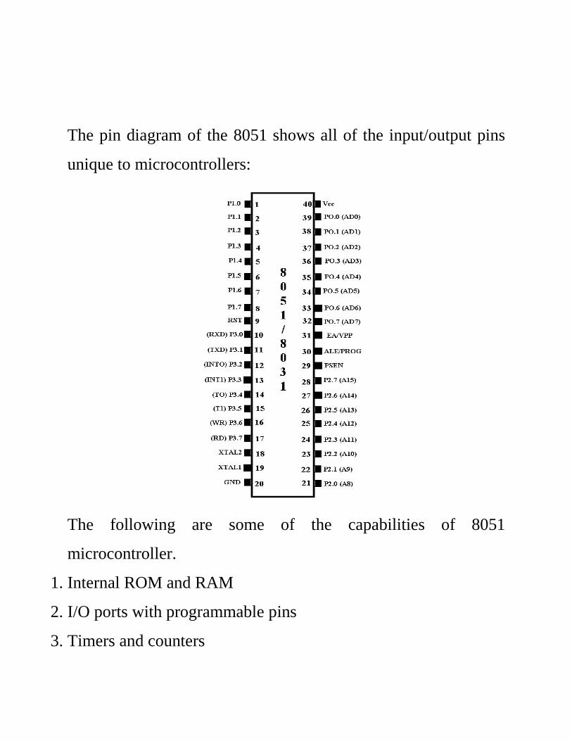
The pin diagram of the 8051 shows all of the input/output pins
unique to microcontrollers:
The following are some of the capabilities of 8051
microcontroller.
1. Internal ROM and RAM
2. I/O ports with programmable pins
3. Timers and counters

4. Serial data communication
The 8051 architecture consists of these specific features:
16 bit PC &data pointer (DPTR)
8 bit program status word (PSW)
8 bit stack pointer (SP)
Internal ROM 4k
Internal RAM of 128 bytes.
4 register banks, each containing 8 registers
80 bits of general purpose data memory
32 input/output pins arranged as four 8 bit ports: P0-P3
Two 16 bit timer/counters: T0-T1
Two external and three internal interrupt sources Oscillator and
clock circuits.


HARDWARE DESCRIPTION:
1. POWER SUPPLY:
Power supply is a reference to a source of electrical power. A
device or system that supplies electrical or other types of energy
to an output load or group of loads is called a power supply
unit or PSU. The term is most commonly applied to electrical
energy supplies, less often to mechanical ones, and rarely to
others. Here in our application we need a 5v DC power supply
for all electronics involved in the project. This requires step
down transformer, rectifier, voltage regulator, and filter circuit
for generation of 5v DC power. Here a brief description of all
the components are given as follows:
TRANSFORMER:
transformer is a device that transfers electrical energy from
one circuit to another through inductively coupled conductors —
the transformer's coils or "windings". Except for air-core
transformers, the conductors are commonly wound around a

single iron-rich core, or around separate but magnetically-
coupled cores. A varying current in the first or "primary"
winding creates a varying magnetic field in the core (or cores) of
the transformer. This varying magnetic field induces a varying
electromotive force (EMF) or "voltage" in the "secondary"
winding. This effect is called mutual induction.
If a load is connected to the secondary circuit, electric charge
will flow in the secondary winding of the transformer and
transfer energy from the primary circuit to the load connected in
the secondary circuit.
The secondary induced voltage VS, of an ideal transformer, is
scaled from the primary VP by a factor equal to the ratio of the
number of turns of wire in their respective windings:

By appropriate selection of the numbers of turns, a transformer
thus allows an alternating voltage to be stepped up — by making
NS more than NP — or stepped down, by making it
BASIC PARTS OF A TRANSFORMER
In its most basic form a transformer consists of:
A primary coil or winding.
A secondary coil or winding.
A core that supports the coils or windings.
Refer to the transformer circuit in figure as you read the
following explanation: The primary winding is connected to a
60-hertz ac voltage source. The magnetic field (flux) builds up
(expands) and collapses (contracts) about the primary winding.
The expanding and contracting magnetic field around the
primary winding cuts the secondary winding and induces an
alternating voltage into the winding. This voltage causes
alternating current to flow through the load. The voltage may be

stepped up or down depending on the design of the primary and
secondary windings.
THE COMPONENTS OF A TRANSFORMER
Two coils of wire (called windings) are wound on some type of
core material. In some cases the coils of wire are wound on a
cylindrical or rectangular cardboard form. In effect, the core
material is air and the transformer is called an AIR-CORE
TRANSFORMER. Transformers used at low frequencies, such
as 60 hertz and 400 hertz, require a core of low-reluctance
magnetic material, usually iron. This type of transformer is
called an IRON-CORE TRANSFORMER. Most power

transformers are of the iron-core type. The principle parts of a
transformer and their functions are:
The CORE, which provides a path for the magnetic lines of flux.
The PRIMARY WINDING, which receives energy from the ac
source.
The SECONDARY WINDING, which receives energy from the
primary winding and delivers it to the load.
The ENCLOSURE, which protects the above components from
dirt, moisture, and mechanical damage.
BRIDGE RECTIFIER
A bridge rectifier makes use of four diodes in a bridge
arrangement to achieve full-wave rectification. This is a widely
used configuration, both with individual diodes wired as shown
and with single component bridges where the diode bridge is
wired internally.

Basic operation
According to the conventional model of current flow originally
established by Benjamin Franklin and still followed by most
engineers today, current is assumed to flow through electrical
conductors from the positive to the negative pole. In actuality,
free electrons in a conductor nearly always flow from the
negative to the positive pole. In the vast majority of
applications, however, the actual direction of current flow is
irrelevant. Therefore, in the discussion below the conventional
model is retained.
In the diagrams below, when the input connected to the left
corner of the diamond is positive, and the input connected to the
right corner is negative, current flows from the upper supply
terminal to the right along the red (positive) path to the output,
and returns to the lower supply terminal via the blue (negative)
path.
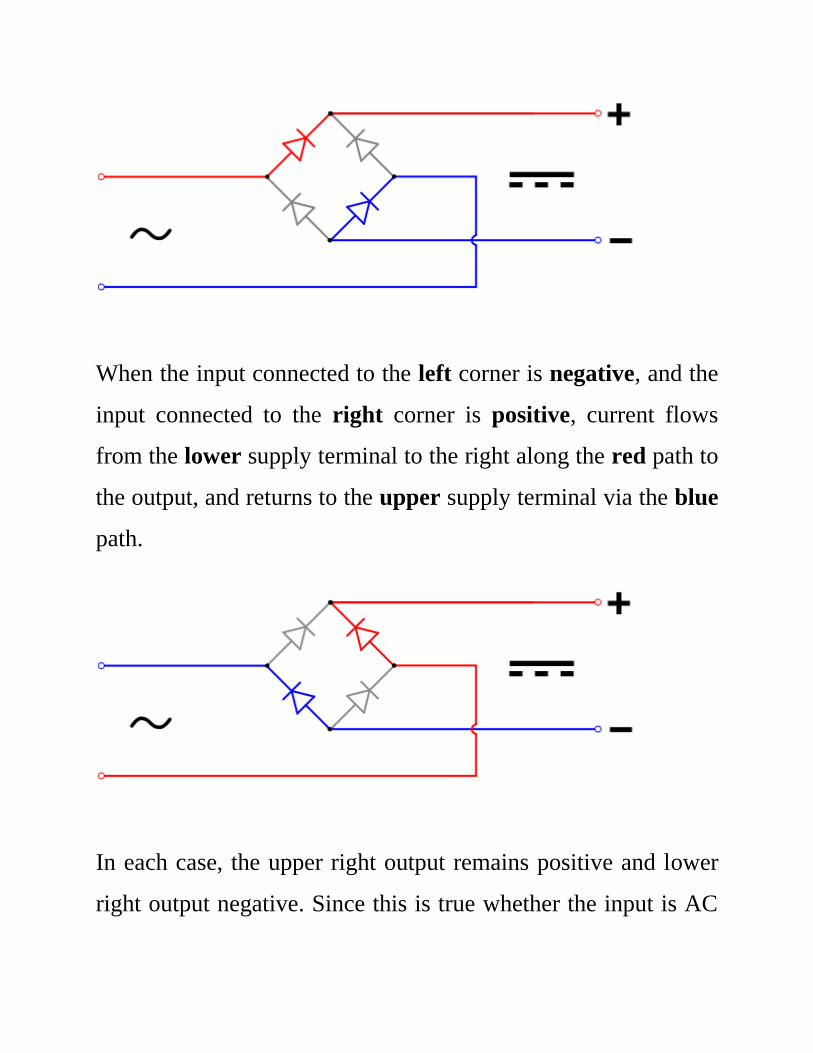
When the input connected to the left corner is negative, and the
input connected to the right corner is positive, current flows
from the lower supply terminal to the right along the red path to
the output, and returns to the upper supply terminal via the blue
path.
In each case, the upper right output remains positive and lower
right output negative. Since this is true whether the input is AC
or DC, this circuit not only produces a DC output from an AC
input, it can also provide what is sometimes called "reverse
polarity protection". That is, it permits normal functioning of
DC-powered equipment when batteries have been installed
backwards, or when the leads (wires) from a DC power source
have been reversed, and protects the equipment from potential
damage caused by reverse polarity.
Prior to availability of integrated electronics, such a bridge
rectifier was always constructed from discrete components.
Since about 1950, a single four-terminal component containing
the four diodes connected in the bridge configuration became a
standard commercial component and is now available with
various voltage and current ratings.
OUTPUT SMOOTHING
For many applications, especially with single phase AC where
the full-wave bridge serves to convert an AC input into a DC
output, the addition of a capacitor may be desired because the
bridge alone supplies an output of fixed polarity but

continuously varying or "pulsating" magnitude (see diagram
above).
The function of this capacitor, known as a reservoir capacitor (or
smoothing capacitor) is to lessen the variation in (or 'smooth')
the rectified AC output voltage waveform from the bridge. One
explanation of 'smoothing' is that the capacitor provides a low
impedance path to the AC component of the output, reducing the
AC voltage across, and AC current through, the resistive load. In
less technical terms, any drop in the output voltage and current
of the bridge tends to be canceled by loss of charge in the
capacitor. This charge flows out as additional current through
the load. Thus the change of load current and voltage is reduced
relative to what would occur without the capacitor. Increases of

voltage correspondingly store excess charge in the capacitor,
thus moderating the change in output voltage / current.
The simplified circuit shown has a well-deserved reputation for
being dangerous, because, in some applications, the capacitor
can retain a lethal charge after the AC power source is removed.
If supplying a dangerous voltage, a practical circuit should
include a reliable way to safely discharge the capacitor. If the
normal load cannot be guaranteed to perform this function,
perhaps because it can be disconnected, the circuit should
include a bleeder resistor connected as close as practical across
the capacitor. This resistor should consume a current large
enough to discharge the capacitor in a reasonable time, but small
enough to minimize unnecessary power waste.
Because a bleeder sets a minimum current drain, the regulation
of the circuit, defined as percentage voltage change from
minimum to maximum load, is improved. However in many
cases the improvement is of insignificant magnitude.
The capacitor and the load resistance have a typical time
constant τ = RC where C and R are the capacitance and load
resistance respectively. As long as the load resistor is large
enough so that this time constant is much longer than the time of
one ripple cycle, the above configuration will produce a
smoothed DC voltage across the load.
In some designs, a series resistor at the load side of the capacitor
is added. The smoothing can then be improved by adding
additional stages of capacitor–resistor pairs, often done only for
sub-supplies to critical high-gain circuits that tend to be
sensitive to supply voltage noise.
The idealized waveforms shown above are seen for both voltage
and current when the load on the bridge is resistive. When the
load includes a smoothing capacitor, both the voltage and the
current waveforms will be greatly changed. While the voltage is
smoothed, as described above, current will flow through the
bridge only during the time when the input voltage is greater
than the capacitor voltage. For example, if the load draws an
average current of n Amps, and the diodes conduct for 10% of
the time, the average diode current during conduction must be
10n Amps. This non-sinusoidal current leads to harmonic
distortion and a poor power factor in the AC supply.
In a practical circuit, when a capacitor is directly connected to
the output of a bridge, the bridge diodes must be sized to
withstand the current surge that occurs when the power is turned
on at the peak of the AC voltage and the capacitor is fully
discharged. Sometimes a small series resistor is included before
the capacitor to limit this current, though in most applications
the power supply transformer's resistance is already sufficient.
Output can also be smoothed using a choke and second
capacitor. The choke tends to keep the current (rather than the
voltage) more constant. Due to the relatively high cost of an
effective choke compared to a resistor and capacitor this is not
employed in modern equipment.
Some early console radios created the speaker's constant field
with the current from the high voltage ("B +") power supply,
which was then routed to the consuming circuits, (permanent
magnets were then too weak for good performance) to create the
speaker's constant magnetic field. The speaker field coil thus
performed 2 jobs in one: it acted as a choke, filtering the power
supply, and it produced the magnetic field to operate the
speaker.

REGULATOR IC (78XX)
It is a three pin IC used as a voltage regulator. It converts
unregulated DC current into regulated DC current.
Normally we get fixed output by connecting the voltage
regulator at the output of the filtered DC (see in above diagram).
It can also be used in circuits to get a low DC voltage from a
high DC voltage (for example we use 7805 to get 5V from 12V).
There are two types of voltage regulators 1. fixed voltage

regulators (78xx, 79xx) 2. variable voltage regulators(LM317)
In fixed voltage regulators there is another classification 1. +ve
voltage regulators 2. -ve voltage regulators POSITIVE
VOLTAGE REGULATORS This include 78xx voltage
regulators. The most commonly used ones are 7805 and 7812.
7805 gives fixed 5V DC voltage if input voltage is in (7.5V,
20V).
The Capacitor Filter
The simple capacitor filter is the most basic type of power
supply filter. The application of the simple capacitor filter is
very limited. It is sometimes used on extremely high-voltage,
low-current power supplies for cathode-ray and similar electron
tubes, which require very little load current from the supply. The
capacitor filter is also used where the power-supply ripple
frequency is not critical; this frequency can be relatively high.
The capacitor (C1) shown in figure 4-15 is a simple filter
connected across the output of the rectifier in parallel with the
load.

Full-wave rectifier with a capacitor filter.
When this filter is used, the RC charge time of the filter
capacitor (C1) must be short and the RC discharge time must be
long to eliminate ripple action. In other words, the capacitor
must charge up fast, preferably with no discharge at all. Better
filtering also results when the input frequency is high; therefore,
the full-wave rectifier output is easier to filter than that of the
half-wave rectifier because of its higher frequency.
For you to have a better understanding of the effect that filtering
has on Eavg, a comparison of a rectifier circuit with a filter and
one without a filter is illustrated in views A and B of figure 4-
16. The output waveforms in figure 4-16 represent the unfiltered
and filtered outputs of the half-wave rectifier circuit. Current
pulses flow through the load resistance (RL) each time a diode
conducts. The dashed line indicates the average value of output
voltage. For the half-wave rectifier, Eavg is less than half (or

approximately 0.318) of the peak output voltage. This value is
still much less than that of the applied voltage. With no
capacitor connected across the output of the rectifier circuit, the
waveform in view A has a large pulsating component (ripple)
compared with the average or dc component. When a capacitor
is connected across the output (view B), the average value of
output voltage (Eavg) is increased due to the filtering action of
capacitor C1.
UNFILTERED
Half-wave rectifier with and without filtering.

FILTERED
The value of the capacitor is fairly large (several microfarads),
thus it presents a relatively low reactance to the pulsating current
and it stores a substantial charge.
The rate of charge for the capacitor is limited only by the
resistance of the conducting diode, which is relatively low.
Therefore, the RC charge time of the circuit is relatively short.
As a result, when the pulsating voltage is first applied to the
circuit, the capacitor charges rapidly and almost reaches the
peak value of the rectified voltage within the first few cycles.
The capacitor attempts to charge to the peak value of the
rectified voltage anytime a diode is conducting, and tends to
retain its charge when the rectifier output falls to zero. (The
capacitor cannot discharge immediately.) The capacitor slowly

discharges through the load resistance (RL) during the time the
rectifier is non-conducting.
The rate of discharge of the capacitor is determined by the value
of capacitance and the value of the load resistance. If the
capacitance and load-resistance values are large, the RC
discharge time for the circuit is relatively long.
A comparison of the waveforms shown in figure 4-16 (view A
and view B) illustrates that the addition of C1 to the circuit
results in an increase in the average of the output voltage (Eavg)
and a reduction in the amplitude of the ripple component (Er)
which is normally present across the load resistance.
Now, let's consider a complete cycle of operation using a half-
wave rectifier, a capacitive filter (C1), and a load resistor (RL).
As shown in view A of figure 4-17, the capacitive filter (C1) is
assumed to be large enough to ensure a small reactance to the
pulsating rectified current. The resistance of RL is assumed to be
much greater than the reactance of C1 at the input frequency.
When the circuit is energized, the diode conducts on the positive
half cycle and current flows through the circuit, allowing C1 to

charge. C1 will charge to approximately the peak value of the
input voltage. (The charge is less than the peak value because of
the voltage drop across the diode (D1)). In view A of the figure,
the charge on C1 is indicated by the heavy solid line on the
waveform. As illustrated in view B, the diode cannot conduct on
the negative half cycle because the anode of D1 is negative with
respect to the cathode. During this interval, C1 discharges
through the load resistor (RL). The discharge of C1 produces the
downward slope as indicated by the solid line on the waveform
in view B. In contrast to the abrupt fall of the applied ac voltage
from peak value to zero, the voltage across C1 (and thus across
RL) during the discharge period gradually decreases until the
time of the next half cycle of rectifier operation. Keep in mind
that for good filtering, the filter capacitor should charge up as
fast as possible and discharge as little as possible.
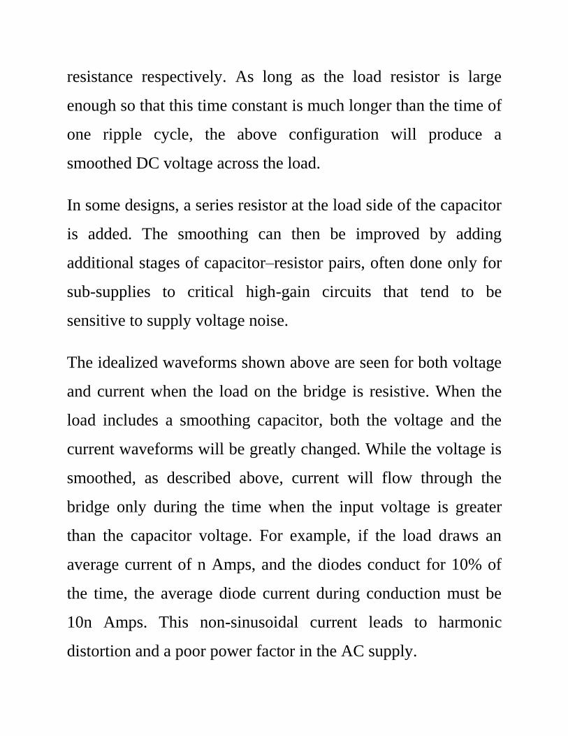
Figure 4-17A. - Capacitor filter circuit (positive and negative
half cycles). POSITIVE HALF-CYCLE
Figure 4-17B. - Capacitor filter circuit (positive and negative
half cycles). NEGATIVE HALF-CYCLE
Since practical values of C1 and RL ensure a more or less
gradual decrease of the discharge voltage, a substantial charge
remains on the capacitor at the time of the next half cycle of
operation. As a result, no current can flow through the diode
until the rising ac input voltage at the anode of the diode exceeds
the voltage on the charge remaining on C1. The charge on C1 is
the cathode potential of the diode. When the potential on the
anode exceeds the potential on the cathode (the charge on C1),
the diode again conducts, and C1 begins to charge to
approximately the peak value of the applied voltage.
After the capacitor has charged to its peak value, the diode will
cut off and the capacitor will start to discharge. Since the fall of
the ac input voltage on the anode is considerably more rapid
than the decrease on the capacitor voltage, the cathode quickly
become more positive than the anode, and the diode ceases to
conduct.
Operation of the simple capacitor filter using a full-wave
rectifier is basically the same as that discussed for the half-wave
rectifier. Referring to figure 4-18, you should notice that
because one of the diodes is always conducting on. either
alternation, the filter capacitor charges and discharges during
each half cycle. (Note that each diode conducts only for that
portion of time when the peak secondary voltage is greater than
the charge across the capacitor.)

Figure 4-18. - Full-wave rectifier (with capacitor filter).
Another thing to keep in mind is that the ripple component (E r)
of the output voltage is an ac voltage and the average output
voltage (Eavg) is the dc component of the output. Since the filter
capacitor offers a relatively low impedance to ac, the majority of
the ac component flows through the filter capacitor. The ac
component is therefore bypassed (shunted) around the load
resistance, and the entire dc component (or Eavg) flows through
the load resistance. This statement can be clarified by using the
formula for XC in a half-wave and full-wave rectifier. First, you
must establish some values for the circuit.


As you can see from the calculations, by doubling the frequency
of the rectifier, you reduce the impedance of the capacitor by
one-half. This allows the ac component to pass through the
capacitor more easily. As a result, a full-wave rectifier output is
much easier to filter than that of a half-wave rectifier.
Remember, the smaller the XC of the filter capacitor with respect
to the load resistance, the better the filtering action. Since
the largest possible capacitor will provide the best filtering.
Remember, also, that the load resistance is an important
consideration. If load resistance is made small, the load current
increases, and the average value of output voltage (Eavg)
decreases. The RC discharge time constant is a direct function of
the value of the load resistance; therefore, the rate of capacitor
voltage discharge is a direct function of the current through the
load. The greater the load current, the more rapid the discharge
of the capacitor, and the lower the average value of output
voltage. For this reason, the simple capacitive filter is seldom
used with rectifier circuits that must supply a relatively large

load current. Using the simple capacitive filter in conjunction
with a full-wave or bridge rectifier provides improved filtering
because the increased ripple frequency decreases the capacitive
reactance of the filter capacitor.
CIRCUIT DIAGRAM OF POWER SUPPLY
DTMF DECODER
Today, most telephone equipment use a DTMF receiver IC. One
common DTMF receiver IC is the Motorola MT8870 that is
widely used in electronic communications circuits. The MT8870
is an 18-pin IC. It is used in telephones and a variety of other
applications. When a proper output is not obtained in projects
using this IC, engineers or technicians need to test this IC
separately. A quick testing of this IC could save a lot of time in
re-search labs and manufacturing industries of communication
instruments. Here’s a small and handy tester circuit for the
DTMF IC. It can be assembled on a multipurpose PCB with an
18-pin IC base. One can also test the IC on a simple breadboard.
For optimum working of telephone equipment, the DTMF
receiver must be designed to recognize a valid tone pair greater
than 40 ms in duration and to accept successive digit tone-pairs
that are greater than 40 ms apart. However, for other
applications like remote controls and radio communications, the
tone duration may differ due to noise considerations. Therefore,
by adding an extra resistor and steering diode the tone duration

can be set to different values. The circuit is configured in
balanced-line mode. To reject common-mode noise signals, a
balanced differential amplifier input is used. The circuit also
provides an excellent bridging interface across a properly
terminated telephone line. Transient protection may be achieved
by splitting the input resistors and inserting ZENER diodes
(ZD1 and ZD2) to achieve voltage clamping. This allows the
transient energy to be dissipated in the resistors and diodes, and
limits the maximum voltage that may appear at the inputs.
Whenever you press any key on your local telephone keypad,
the delayed steering (Std) output of the IC goes high on
receiving the tone-pair, causing LED5 (connected to pin 15 of
IC via resistor R15) to glow. It will be high for a duration de-
pending on the values of capacitor and resistors at pins 16 and
17. The optional circuit shown within dot-ted line is used for
guard time adjustment.
The LEDs connected via resistors R11 to R14 at pins 11 through
14, respectively, indicate the output of the IC. The tone-pair
DTMF (dual-tone multi-frequency) generated by pressing the
telephone button is converted into bi-nary values internally in

the IC. The binary values are indicated by glowing of LEDs at
the output pins of the IC. LED1 represents the lowest signifi-
cant bit (LSB) and LED4 represents the most significant bit
(MSB). So, when you dial a number, say, 5, LED1 and LED3
will glow, which is equal to 0101. Similarly, for every other
number dialed on your telephone, the corresponding LEDs will
glow. Thus, a non-defective IC should indicate proper bi-nary
values corresponding to the decimal number pressed on your
telephone key-pad.
To test the DTMF IC 8870/KT3170, proceed as follows:
Connect local telephone and the circuit in parallel to the
same telephone line.
Switch on S1. (Switch on auxiliary switch S2 only if keys
A, B, C, and D are to be used.)
Now push key ‘*’ to generate DTMF tone.
Push any decimal key from the telephone keypad.

Observe the equivalent binary as shown in the table.
If the binary number implied by glowing of LED1 to LED4
is equivalent to the pressed key number (decimal/A, B, C,
or D), the DTMF IC 8870 is correct.
Keys A, B, C, and D on the telephone keypad are used for
special signaling and are not available on standard pushbutton
telephone keypads. Pin 5 of the IC is pulled down to ground
through resistor R8. Switch on auxiliary switch S2. Now the
high logic at pin 5 enables the detection of tones representing
characters A, B, C, and D.

DIODE
The diode is a p-n junction device. Diode is the component
used to control the flow of the current in any one direction. The
diode widely works in forward bias.
Diode When the current flows from the P to N direction. Then it
is in forward bias. The Zener diode is used in reverse bias
function i.e. N to P direction. Visually the identification of the
diode`s terminal can be done by identifying he silver/black line.
The silver/black line is the negative terminal (cathode) and the
other terminal is the positive terminal (cathode).
APPLICATION
•Diodes: Rectification, free-wheeling, etc
•Zener diode: Voltage control, regulator etc.

•Tunnel diode: Control the current flow, snobbier circuit, etc
RESISTORS
The flow of charge through any material encounters an
opposing force similar in many respects to mechanical friction
.this opposing force is called resistance of the material .in some
electric circuit resistance is deliberately introduced in form of
resistor. Resistor used fall in three categories , only two of
which are color coded which are metal film and carbon film
resistor .the third category is the wire wound type ,where value
are generally printed on the vitreous paint finish of the
component. Resistors are in ohms and are represented in Greek
letter omega, looks as an upturned horseshoe. Most electronic
circuit require resistors to make them work properly and it is
obliviously important to find out something about the different
types of resistors available. Resistance is measured in ohms, the
symbol for ohm is an omega ohm. 1 ohm is quite small for
electronics so resistances are often given in kohm and Mohm.
Resistors used in electronics can have resistances as low as 0.1
ohm or as high as 10 Mohm.

FUNCTION
Resistor restrict the flow of electric current, for example a
resistor is placed in series with a light-emitting diode(LED) to
limit the current passing through the LED.
TYPES OF RESISTORS
FIXED VALUE RESISTORS
It includes two types of resistors as carbon film and metal film
.These two types are explained under
CARBON FILM RESISTORS
During manufacture, at in film of carbon is deposited onto a
small ceramic rod. The resistive coating is spiraled away in an
automatic machine until the resistance between there two ends
of the rods is as close as possible to the correct value. Metal
leads and end caps are added, the resistors is covered with an

insulating coating and finally painted with colored bands to
indicate the resistor value
Carbon Film Resistors
Another example for a Carbon 22000 Ohms or 22 Kilo-Ohms
also known as 22K at 5% tolerance: Band 1 = Red, 1st digit
Band 2 = Red, 2nd digit Band 3 = Orange, 3rd digit, multiply
with zeros, in this case 3 zero's Band 4 = Gold, Tolerance, 5%
METAL FILM RESISTORS
Metal film and metal oxides resistors are made in a similar way,
but can be made more accurately to within ±2% or ±1% of their
nominal vale there are some difference in performance between
these resistor types, but none which affects their use in simple
circuit.

WIRE WOUND RESISTOR
A wire wound resistor is made of metal resistance wire, and
because of this, they can be manufactured to precise values.
Also, high wattage resistors can be made by using a thick wire
material. Wire wound resistors cannot be used for high
frequency circuits. Coils are used in high frequency circuit. Wire
wound resistors in a ceramic case, strengthened with special
cement. They have very high power rating, from 1 or 2 watts to
dozens of watts. These resistors can become extremely hot when
used for high power application, and this must be taken into
account when designing the circuit.
TESTING
Resistors are checked with an ohm meter/millimeter. For a
defective resistor the ohm-meter shows infinite high reading.
CAPACITORS
In a way, a capacitor is a little like a battery. Although they
work in completely different ways, capacitors and batteries both
store electrical energy. If you have read How Batteries Work ,

then you know that a battery has two terminals. Inside the
battery, chemical reactions produce electrons on one terminal
and absorb electrons at the other terminal.
BASIC
Like a battery, a capacitor has two terminals. Inside the
capacitor, the terminals connect to two metal plates separated by
a dielectric. The dielectric can be air, paper, plastic or anything
else that does not conduct electricity and keeps the plates from
touching each other. You can easily make a capacitor from two
pieces of aluminum foil and a piece of paper. It won't be a
particularly good capacitor in terms of its storage capacity, but it
will work.
In an electronic circuit, a capacitor is shown like this:
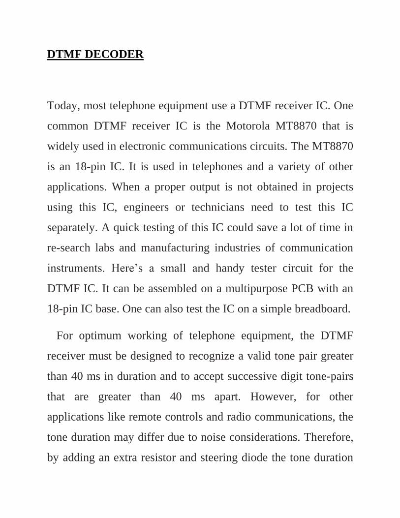
When you connect a capacitor to a battery, here’s what happens:
•The plate on the capacitor that attaches to the negative terminal
of the battery accepts electrons that the battery is producing.
•The plate on the capacitor that attaches to the positive terminal
of the battery loses electrons to the battery.
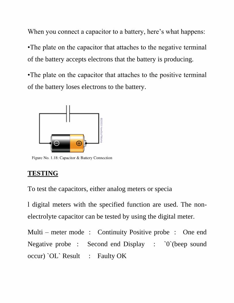
TESTING
To test the capacitors, either analog meters or specia
l digital meters with the specified function are used. The non-
electrolyte capacitor can be tested by using the digital meter.
Multi – meter mode : Continuity Positive probe : One end
Negative probe : Second end Display : `0`(beep sound
occur) `OL` Result : Faulty OK

LED
LED falls within the family of P-N junction devices. The light
emitting diode (LED) is a diode that will give off visible light
when it is energized. In any forward biased P-N junction there
is, with in the structure and primarily close to the junction, a
recombination of hole and electrons. This recombination
requires that the energy possessed by the unbound free electron
be transferred to another state. The process of giving off light by
applying an electrical source is called electroluminescence.
LED is a component used for indication. All the functions being
carried out are displayed by led .The LED is diode which glows
when the current is being flown through it in forward bias

condition. The LEDs are available in the round shell and also in
the flat shells. The positive leg is longer than negative leg.
DC MOTOR
DC Motor has two leads. It has bidirectional motion
If we apply +ve to one lead and ground to another motor
will rotate in one direction, if we reverse the connection the
motor will rotate in opposite direction.
If we keep both leads open or both leads ground it will not
rotate (but some inertia will be there).
If we apply +ve voltage to both leads then braking will
occurs.
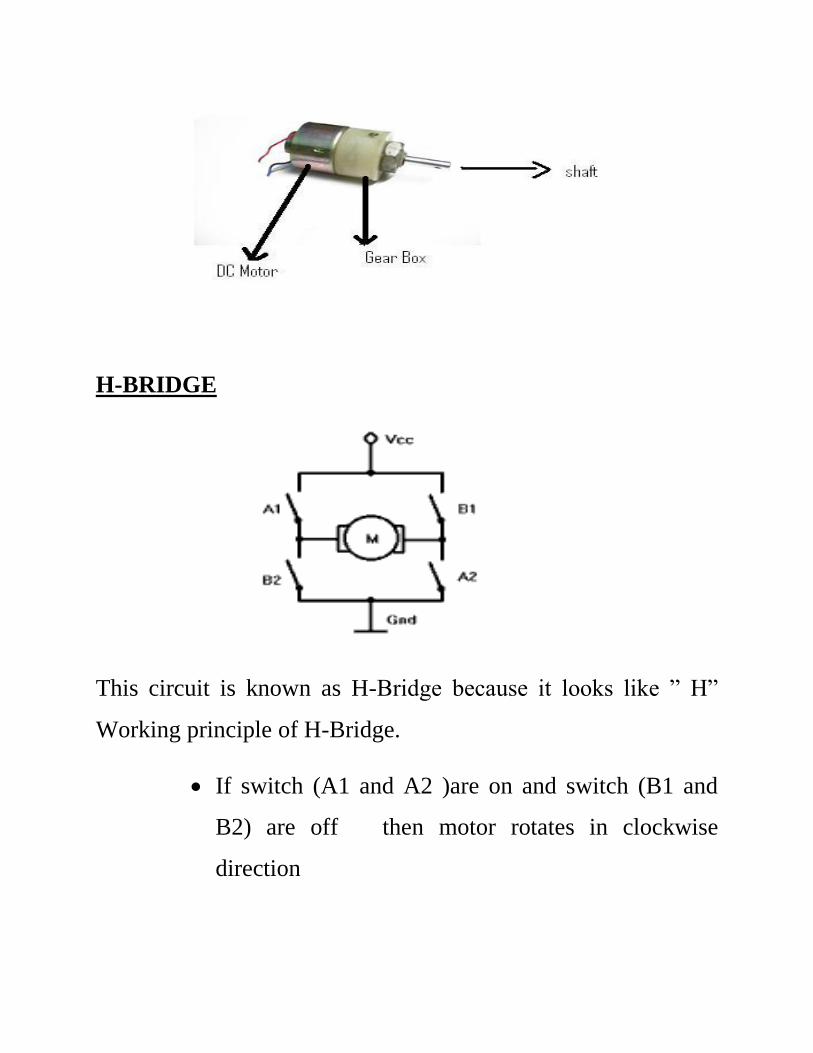
H-BRIDGE
This circuit is known as H-Bridge because it looks like ” H”
Working principle of H-Bridge.
If switch (A1 and A2 )are on and switch (B1 and
B2) are off then motor rotates in clockwise
direction
If switch (B1 and B2 )are on and switch (A1 and
A2) are off then motor rotates in Anti clockwise
direction
we can use Transistor, mosfets as a switch ( Study
the transistor as a a switch)
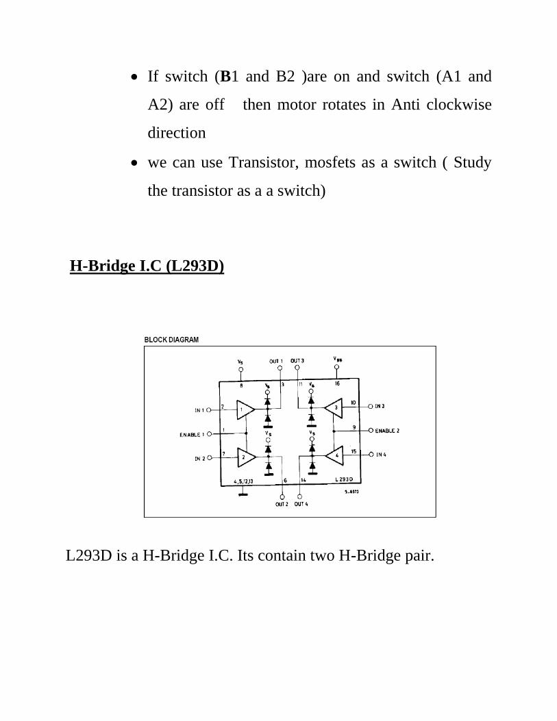
H-Bridge I.C (L293D)
L293D is a H-Bridge I.C. Its contain two H-Bridge pair.

Truth Table
Input 1 Input 2 Result
0 0 No rotation
0 1 Clockwise rotation
1 0 Anti clockwise
rotation
1 1 break
Note:-
Connect motors pins on output 1 and output 2 and control
signal at input 1 and input 2 will control the motion
Connect another motor pins on output 3 and output 4 and
control signal at input3and input 4
Truth table for i/p 3 and i/p 4 is same as above shown
0 means 0 V or Low
1 means High or +5V
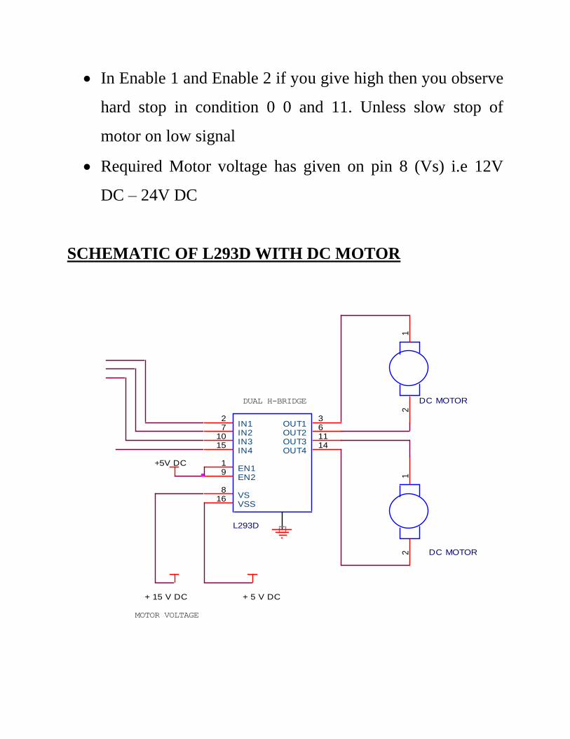
In Enable 1 and Enable 2 if you give high then you observe
hard stop in condition 0 0 and 11. Unless slow stop of
motor on low signal
Required Motor voltage has given on pin 8 (Vs) i.e 12V
DC – 24V DC
SCHEMATIC OF L293D WITH DC MOTOR
+ 15 V DC
MOTOR VOLTAGE
L293D
27
1015
19
361114
168
IN1IN2IN3IN4
EN1EN2
OUT1OUT2OUT3OUT4
VSSVS
+5V DC
DUAL H-BRIDGE
+ 5 V DC
DC MOTOR
12
DC MOTOR 1
2

μVISION
The μ Vision IDE is, for most developers, the easiest way to
create embedded system programs. This chapter describes
commonly used μ Vision features and explains how to use them.
General Remarks and Concepts
Before we start to describe how to use μVision, some general
remarks, common to many screens1 and to the behavior of the
development tool, are presented. In our continuous effort to
deliver best-in-class development tools, supporting you in your
daily work, μVision has been built to resemble the look-and-feel
of widespread applications. This approach decreases your
learning curve, such that
you may start to work with μ Vision right away.
Based on the concept of windows:

μ Vision windows can be re-arranged, tiled, and attached to
other screen areas or windows respectively It is possible to drag
and drop windows, objects, and variables
A Context Menu, invoked through the right mouse button, is
provided for most objects. You can use keyboard shortcuts and
define your own shortcuts. You can use the abundant features of
a modern editor. Menu items and Toolbar buttons are greyed out
when not available in the Current context.
Graphical symbols are used to resemble options, to mark
unsaved changes, or reveal objects not included into the project.
Status Bars display context-driven information. You can
associate μVision to third-party tools
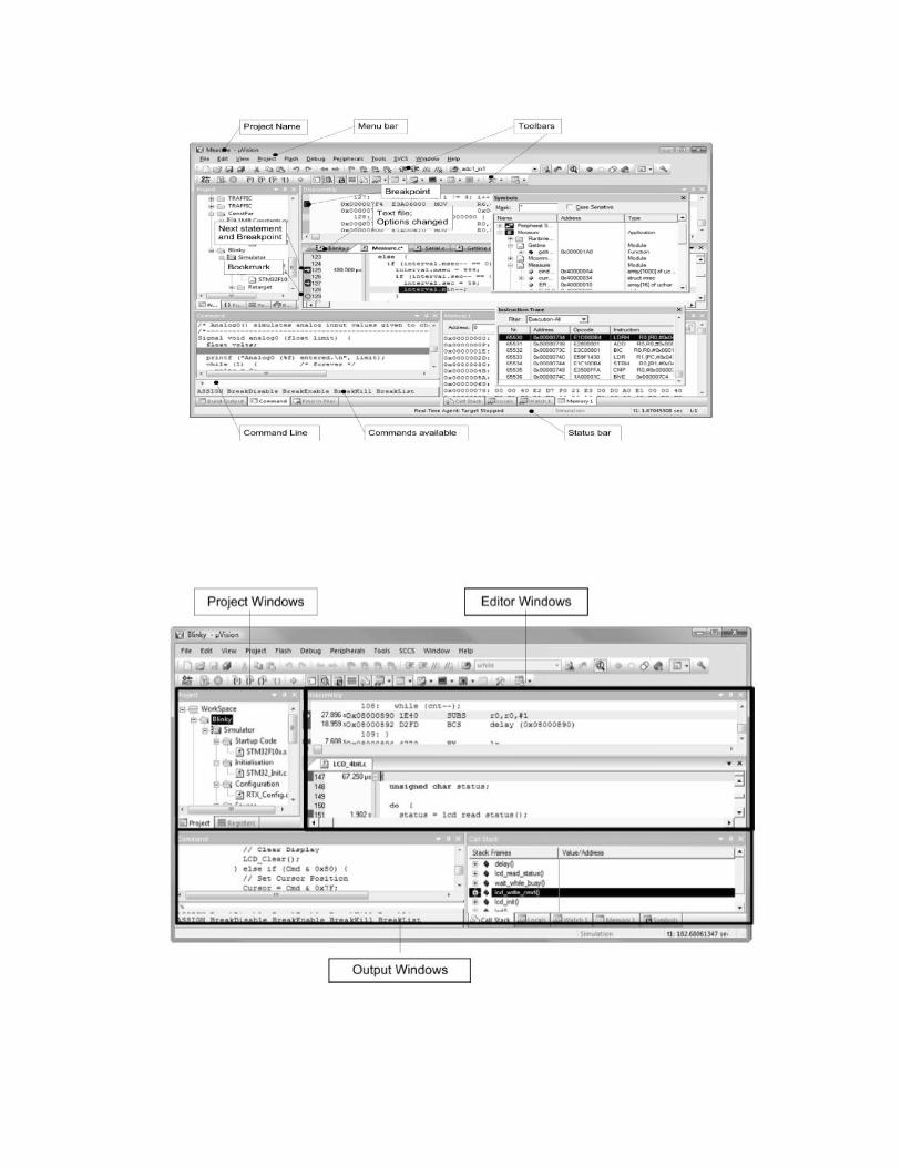

The Project Windows area is that part of the screen in which,
by default, the Project Window, Functions Window, Books
Window, and Registers Window are displayed.
Within the Editor Windows area, you are able to change the
source code, view performance and analysis information, and
check the disassembly code.
The Output Windows area provides information related to
debugging, memory, symbols, call stack, local variables,
commands, browse information, and find in files results.
If, for any reason, you do not see a particular window and have
tried displaying/hiding it several times, please invoke the default
layout of μVision through the Window – Reset Current
Layout Menu.
Positioning Windows
The μVision windows may be placed onto any area of the
screen, even outside of the μVision frame, or to another physical
screen.

Click and hold the Title Bar1 of a window with the left mouse
button
Drag the window to the preferred area, or onto the preferred
control, and release the mouse button
Please note, source code files cannot be moved outside of the
Editor Windows2.\ Invoke the Context Menu of the window’s
Title Bar to change the docking attribute of a window object. In
some cases, you must perform this action before you can drag
and drop the window.
μVision displays docking helper controls3, emphasizing the area
where the window will be attached. The new docking area is
represented by the section highlighted in blue. Snap the window
to the Multiple Document Interface (MDI) or to a Windows area
by moving the mouse over the preferred control.

Keil software converts the C-codes into the Intel Hex code.
A view of Keil uVision 3

A view of Keil uVision 3

8051 Burner Software
PRO51 BURNER provides you with software burning tools for
8051 based Microcontrollers in there Flash memory. The 51
BURNER tools, you can burn AT89SXXXX series of ATMEL
microcontrollers.

PRO 51
PRO51 - Programmer for C51 family
Features of PRO51
Flash Programmer for 89C1051, 89C2051, 89C4051, 89S51,
89S52, 89C51 and 89C52 micros.
Operates on single 5V supply which can be taken from USB
Port of PC.
User friendly windows based Graphics User Interface.
Interfaces with PC through COM1 or COM2 serial ports.
System Requirements
PC with at least one serial and one USB ports and at least
600x800 VGA resolution.
If USB port is not available you need a regulated +5V supply.
Windows operating system

Package Contents
PRO51 unit
Interface Cable between PC and PRO51
CD containing PROG51 software
Getting Started
1. Install PROG51 programs using setup from the CD. This would
normally create these programs in a program group INFONICS.
You may like to create a separate folder like INFONICS on your
disk where these programs will be installed.
2. Connect PRO51 to COM port and USB on your PC using the Y
cable provided with PRO51. Follow instruction given in the
following sections.
PROG51 User Interface

Prog51 is used for programming the 89C1051, 89C2051 and
89C4051 Microcontrollers. User interface includes:
Load Hex/Binary file in Buffer
Save Buffer as Binary File
Display / Specify Target Device to be Programmed.
Com Port Selection.
Identify Target Device with the device specified by you in the
designated area.
Read Microcontroller Program in Buffer
Erase Microcontroller Program Memory
Check if Target Device is Erased
Program Buffer Contents in Target device
Verify the Device contents with data in the buffer
3. Lock Target Device. Once the device is locked it can not be read
or verified.

Procedure to Program a Chip
1. Connect the PRO51 to COM port and USB port on your PC.
USB is used for +5V power supply only. You can use regulated
5V supply and connect it on pin 4 of the 9 Pin connector.
2. Start PROG51 from your program menu.
3. Select appropriate com port on your PC.
4. Insert desired device in the ZIF socket on PRO51. 20 Pin
devices like 89C2051 should be aligned with the bolltom side,

i.e., pin 10 on the 89C2051 should be inserted in Pin 20 of the
socket.
5. Specify the device in the target device text box.
6. Click Identify button to check if the device inserted matches
with the one you specified in the Target Device text box.
7. Load Hex or Binary file generated using compiler or assembler
in the buffer.
8. Click on Erase button to erase the contents of the flash memory
of the microcontroller. Erase process will automatically be
followed by a blank check.
9. Click on Program button to write the buffer contents in to the
program memory of the microcontroller. Program action will
automatically be followed by a verify cycle.
10. If you wish click on Lock button to secure the device.
11. Remove the device from ZIF socket.

Block Diagram of PRO51
ZIF Socket
RST RXD TXD
Programmer
Power
Supply
3
2
6
8
4
5

Pin description of 9 PIN male connector on PRO51
Pin Name Description
1 NC Not connected
2 RXD Serial Port Receive Data. This pin should
be connected to TXD pin of COM port on
PC.
3 TXD Serial Port Transmit Data. This pin should
be connected to RXD pin of COM port on
PC.
4 VCC +5V supply for the PRO51. It must be
regulated supply. Cable supplied with the
device draws power from the USB port of
your PC. If you wish to use any other
source of power the same should be
connected to this pin.
5 GND Signal and power ground for serial port
and 5V power supply.

6 RXDEN If this pin is left open or pulled up (>3V)
then RXD signal received at PIN 2 above
is sent to the CPU. If you wish to disable
the RXD signal then this PIN should be
pulled –Ve. With the standard cable
supplied by Infonics this pin is connected
to the DSR signal of COM port.
Therefore, the DSR must high to enable
the RXD.
7 NC Not connected
8 RESET A high (> 3V) on this pin will reset the
PRO51. With the standard cable supplied
by Infonics this pin is connected to the
RTS signal of COM port. Therefore, the
RTS must be kept low for proper
operation of the PRO51. A high pulse on
RTS can be used to reset the device.
9 NC Not connected
CONSTRUCTION AND TESTING
CONSTRUCTION
In the process of realizing this project, the construction was
initially carried out on a breadboard to allow for checking and to
ascertain that it is functioning effectively. All irregularities were
checked then tested and found to have a satisfactory output. The
component were then removed and transferred to a Vero board
strip and soldered into place and all discontinuous point were cut
out to avoid short-circuiting.
PRECAUTIONS
SOLDERING PRECAUTIONS
The construction was carried out with care. The precautions
taken during the soldering were:
The tip of soldering iron was kept clean with the help of a file
from time to time.
The solder wire was of smaller thickness.

Extra solder was not used in order to avoid a cause of short
circuit in the conductive path.
The overheating of components was avoided to prevent
component damage as a result of excessive heat on the
components due to the heat from the soldering iron.
The leads of the components were kept clean before soldering,
with the use of sand paper.
COMPONENTS PRECAUTION:
IR sensor used should be sensitive. Before using in the
circuit it should be tested with a multi-meter.
I.C should not be heated much while soldering; too much
heat can destroy the I.C. For safety and ease of
replacement, the use of I.C socket is suggested.
While placing the I.C pin no 1 should be made sure at
right hole.
Opposite polarity of battery can destroy I.C so please
check the polarity before switching ON the circuit. One

should use diode in series with switch for safety since
diode allows flowing current in one direction only.
Each component was soldered neatly and clean.
We should use insulated wires.
TESTING OF PROJECT
With the knowledge of operation of the system was tested step
by step to the transistor output and the load was connected
across the collector terminal of the transistor.
ASSEMBLING
The whole system was packed in a plastic casing and provision
was made for the IR to sense light from the outside.

REFERENCES
“8051 and embedded system” by Mazidi and Mazidi
All datasheets from www.datasheetcatalog.com
About AT89s8252 from www.atmel.com
And www.triindia.co.in