Embed Size (px)
Citation preview
998 IEEE TRANSACTIONS ON MAGNETICS, VOL. 28, NO. 2, MARCH 1992
Domains and Domain Nucleation in Magnetron-Sputtered CoCr
Thin Films B. G. Demczyk
Abstract-The magnetic domain configurations in magne- tron-sputtered CoCr thin films have been examined by Lorentz transmission electron microscopy. The thinnest (10 nm) films display in-plane 180” domain walls, while thicker (50 nm) films exhibit out-of-plane “dot”- type domain structures. The “dot” domains were observed even in films that had not yet developed a columnar morphology. Intermediate thickness films show a “feather-like” contrast, indicating that both in-plane and out- of-plane magnetization components are present. Magnetization reversal is seen to occur by domain wall motion in films dis- playing in-plane anisotropy and by rotation for perpendicular anisotropy films. Intrinsic film stress was found to play a major role in determining the preferred magnetization direction, and thus the resulting magnetic domain configurations.
I. INTRODUCTION HIN films of CoCr have been of interest for a number T of years due to their strong perpendicular anisotropy,
favoring magnetization normal to the film plane [ 11, [2]. The microstructure and magnetic properties of CoCr films prepared by both RF and magnetron sputtering have been examined in detail [3]-[ 101. In one of the earlier magnetic domain studies of CoCr thin films, Ouchi and Iwasaki [ 111 observed stripe and maize configurations in RF-sputtered CoCr films, and related the domain period to that of ob- served structural columns, thus implying single-column domains. Ohkoshi et al. [12] reported (in RF-sputtered films) a transition from in-plane cross-tie walls to a “dot” structure as the magnetization M became increasingly fa- vored to lie normal to the film plane. In this case, struc- tural columns were presumed to behave as a magnetic cluster. Magnetization reversal would then proceed by ro- tational switching in individual columns. Both Grundy and Ali [4] (dc triode-sputtered) and Hoffman et al. [13] (RF-sputtered) saw a transition from “feather-like” do- main ripples to magnetic “dot” domains with increasing film thickness (and, consequently, M increasingly favored to lie out of the film plane). Lee et al. [14] reported the
Manuscript received August 12, 1991; revised November 15, 1991. This work was supported in part by the Division of Materials Research, National Science Foundation under Grant DMR-8613386. This paper was presented at the 5th Joint MMM-INTERMAG Conference, Pittsburgh, PA, June 1991.
The author is with the North Campus Electron Microbeam Analysis Lab- oratory, Department of Materials Science and Engineering, University of Michigan, Ann Arbor, MI 48109.
IEEE Log Number 9105874.
full range of domain structures (in-plane to “feather-like” to “dot” configurations) in magnetron-sputtered CoCr films. In a number of these works, attempts were made to correlate these domain configurations with the degree of hexagonal close packed c-axis texturing normal to the film plane, thereby attributing the perpendicular magnetiza- tion components to the magnetocrystalline anisotropy. Hoffman [ 131, however, recognized that perpendicular magnetization was present, even when K, < 47rMs, where K, is the magnetocrystalline anisotropy and M, is the sat- uration magnetization. In no cases, however, were mag- netoelastic anisotropy contributions considered. In the present work, the evolution of the magnetic domain struc- tures in magnetron-sputtered CO-22 at% Cr thin films of known microstructure were examined by Lorentz trans- mission electron microscopy. In addition, the operative magnetization reversal mechanism in different film thick- ness regimes was investigated through in situ domain nu- cleation studies. Observations were related to concurrent in-plane stress measurements [ 151, [ 171 to illustrate stress effects on the net magnetization, and thus the resulting magnetic domain structures in these films.
11. EXPERIMENTAL Thin-film specimens of thickness 5-50 nm were pre-
pared by depositing directly onto carbon-coated 3 mm copper grids using a Varian dc mangetron (“S” gun) sputtering system. Sputtering conditions included an ar- gon pressure of 1 mtorr, unheated substrates, and a sput- tering rate of 0.25 nm/s. Conventional transmission elec- tron microscopy (TEM) was performed on a JEOL 2000FX transmission electron microscope, operating at 200 kV. Magnetic domains were imaged in the Fresnel Lorentz TEM mode [16]. In this mode of operation, the field applied by the microscope objective lens at the back focal plane was less than 5 Oe. In situ domain heating studies, utilizing a Gatan model 628 heating holder, were undertaken at temperatures up to -6OO”C, as measured by the specimen holder thermocouple.
111. RESULTS AND DISCUSSION A. Domain ConJgurations
Fig. 1 (a)-(d) illustrate the magnetic domain structures of the as-deposited, demagnetized specimens. At 10 nm
0018-9464/92$03.00 0 1992 IEEE
DEMCZYK: DOMAINS & DOMAIN NUCLEATION I N CoCr THIN FILMS 999
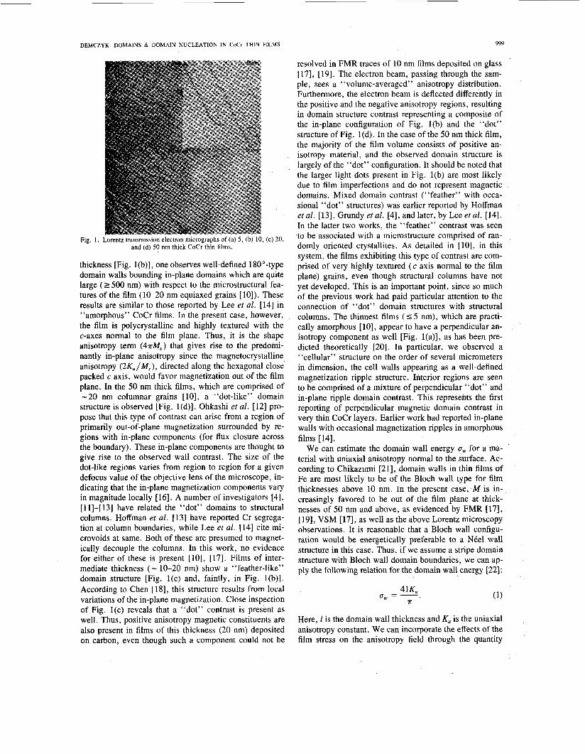
Fig. 1. Lorentz transmission electron micrographs of (a) 5 , (b) 10, (c) 20, and (d) 50 nm thick CoCr thin films.
thickness [Fig. l(b)], one observes well-defined 1 SOo-type domain walls bounding in-plane domains which are quite large (2500 nm) with respect to the microstructural fea- tures of the film (10-20 nm equiaxed grains [lo]). These results are similar to those reported by Lee et a2. [14] in “amorphous” CoCr films. In the present case, however, the film is polycrystalline and highly textured with the c-axes normal to the film plane. Thus, it is the shape anisotropy term (4nM,) that gives rise to the predomi- nantly in-plane anisotropy since the magnetocrystalline anisotropy (2K,/ M3), directed along the hexagonal close packed c axis, would favor magnetization out of the film plane. In the 50 nm thick films, which are comprised of -20 nm columnar grains [lo], a “dot-like’’ domain structure is observed [Fig. l(d)]. Ohkashi et al. [12] pro- pose that this type of contrast can arise from a region of primarily out-of-plane magnetization surrounded by re- gions with in-plane components (for flux closure across the boundary). These in-plane components are thought to give rise to the observed wall contrast. The size of the dot-like regions varies from region to region for a given defocus value of the objective lens of the microscope, in- dicating that the in-plane magnetization components vary in magnitude locally [ 161. A number of investigators [4], [ 111-[13] have related the “dot” domains to structural columns. Hoffman et al. [13] have reported Cr segrega- tion at column boundaries, while Lee et al. [14] cite mi- crovoids at same. Both of these are presumed to magnet- ically decouple the columns. In this work, no evidence for either of these is present [lo], [17]. Films of inter- mediate thickness ( - 10-20 nm) show a “feather-like’’ domain structure [Fig. l(c) and, faintly, in Fig. l(b)]. According to Chen [ 181, this structure results from local variations of the in-plane magnetization. Close inspection of Fig. l(c) reveals that a “dot” contrast is present as well. Thus, positive anisotropy magnetic constituents are also present in films of this thickness (20 nm) deposited on carbon, even though such a component could not be
resolved in FMR traces of 10 nm films deposited on glass [17], [19]. The electron beam, passing through the sam- ple, sees a “volume-averaged’’ anisotropy distribution. Furthermore, the electron beam is deflected differently in the positive and the negative anisotropy regions, resulting in domain structure contrast representing a composite of the in-plane configuration of Fig. l(b) and the “dot” structure of Fig. l(d). In the case of the 50 nm thick film, the majority of the film volume consists of positive an- isotropy material, and the observed domain structure is largely of the “dot” configuration. It should be noted that the larger light dots present in Fig. l(b) are most likely due to film imperfections and do not represent magnetic domains. Mixed domain contrast (“feather” with occa- sional “dot” structures) was earlier reported by Hoffman et al. [ 131, Grundy et al. [4], and later, by Lee et al. [ 141. In the latter two works, the “feather” contrast was seen to be associated with a microstructure comprised of ran- domly oriented crystallites. As detailed in [lo], in this system, the films exhibiting this type of contrast are com- prised of very highly textured ( c axis normal to the film plane) grains, even though structural columns have not yet developed. This is an important point, since so much of the previous work had paid pafticular attention to the connection of “dot” domain structures with structural columns. The thinnest films (I 5 nm), which are practi- cally amorphous [lo], appear to have a perpendicular an- isotropy component as well [Fig. l(a)], as has been pre- dicted theoretically [20]. In particular, we observed a “cellular” structure on the order of several micrometers in dimension, the cell walls appearing as a well-defined magnetization ripple structure. Interior regions are seen to be comprised of a mixture of perpendicular “dot” and in-plane ripple domain contrast. This represents the first reporting of perpendicular magnetic domain contrast in very thin CoCr layers. Earlier work had reported in-plane walls with occasional magnetization ripples in amorphous films [14].
We can estimate the domain wall energy uw for a ma- terial with uniaxial anisotropy normal to the surface. Ac- cording to Chikazumi [21], domain walls in thin films of Fe are most likely to be of the Bloch wall type for film thicknesses above 10 nm. In the present case, M is in- creasingly favored to be out of the film plane at thick- nesses of 50 nm and above, as evidenced by FMR [17], [ 191, VSM [ 171, as well as the above Lorentz microscopy observations. It is reasonable that a Bloch wall configu- ration would be energetically preferable to a NCel wall structure in this case. Thus, if we assume a stripe domain structure with Bloch wall domain boundaries, we can ap- ply the following relation for the domain wall energy [22]:
41K, U, = -.
n
Here, 1 is the domain wall thickness and K, is the uniaxial anisotropy constant. We can incorporate the effects of the film stress on the anisotropy field through the quantity

IEEE TRANSACTIONS ON MAGNETICS, VOL. 28, NO. 2. MARCH 1992
H k e f f , defined as
with U the in-plane film stress and A, the saturation mag- netostriction constant. Using Hkeff = 1.6 kOe [ 171 and M, = 300 emu/cm3 [17], we can compute a K* of 8.05 X lo5 erg/cm3. Using this value in place of K, in ( l ) , along with 1 = 5.6 nm (Table I), we obtain a U, of 5.7 X
J/m2, compared to values of U, = 1 x J/m2 [2] and U,,, = 2.2 X J/m2 [23] cited in the literature. It should be noted that the latter values were determined without considering the effects of the film stress on the anisotropy field. We have also computed an arbitrary ‘‘domain size” for samples displaying out-of-plane mag- netization by subtracting twice the measured domain wall width from that of the total region encompassing the “dot” domain plus its surrounding domain walls. These values are shown in Table I , and are seen to be on the order of a few times the average grain size, as tabulated in [ 101. Thus, it appears that the film is composed of do- mains, comprising, at most, a few columns. This is con- sistent with observed easy axis hysteresis loops [17], which support an incoherent rotation mechanism. In-plane domain wall widths [Fig. l(b) and (c)] are 10 nm or more. The equilibrium domain width d can be obtained by min- imizing the total energy of the stripe domain structure, given by the sum of the demagnetizing energy Ed - 0.136 mod/h M: [22] (valid for d < t) and the domain wall energy per unit volume E, = u,/d. Here, po is the permeability of free space and t is the film thickness. Solving for U,,,, one obtains [2]
(3) U, = ~
(2.7)2t ’
Using the experimentally determined values of d = 27.5 and 50 nm, for the 10 and 50 nm thick films, respectively, along with M, = 300 erg/cm3 [17], we obtain values of o,,, of 1.2 and 7.75 x J/m2 from (3). These values are in reasonable agreement with both the literature values quoted above and the value derived from (1). This attests to the validity and internal consistency of the measure- ments. The spacing between domain walls for the in- plane magnetization films was found to be much larger (2 100 nm) than for the out-of-plane domains and is many times the observed grain size. This is similar to the do- main periods previously reported by Grundy et al. [4] and somewhat less than the 0.5-1 pm periods quoted by Ouchi et al. [ l l ] and Ohkoshi et al. [12].
d2 @Po
.
B. Domain Nucleation Fig. 2 depicts an in situ heatinglcooling sequence per-
formed on a 10 nm thick CoCr film. As shown, the orig- inal in-plane domains [compare to Fig. l(b)] are seen to retract upon heating [Fig. 2(a)-(e)], leaving a residual magnetization ripple [Fig. 2(f)]. It should be noted that this ripple contrast persisted, even up to a temperature of
TABLE I MAGNETIC DOMAIN PARAMETERS ( t = FILM THICKNESS, 1 = DOMAIN
WALL THICKNESS, d = DOMAIN WIDTH)
5 I O 50
I O + 2.6 5 .6
loo+ 21.5 50
Fig. 2 . Lorentz electron micrographs of 10 nm thick CoCr thin film de- picting: (a)-(f ) heating (T,,, = 600”C), (g)-(i) cooling sequence.
600°C, as read on the specimen holder thermocouple. Heating to higher temperatures resulted in a phase trans- formation to the nonmagnetic face centered cubic form, with consequent loss of all domain contrast. In situ ob- servations of this heating sequence very clearly displayed that the domain walls move in definite, finite jumps. This observation is consistent with previous results on these same films [17], in which it was concluded, based on magnetization data, that the reversal mechanism for films with in-plane anisotropy was wall motion. Upon cooling, the ripple contrast intensified, but no in-plane domains appeared [Fig. 2(g)-(i)]. However, cycling to a somewhat lower maximum temperature (450°C) did result in the reemergence of in-plane domains. Similar results appear to have been observed by Jeong and Walser [24] in amor- phous Co61B39 films.
In Fig. 3, a similar heatinglcooling sequence for a 50 nm thick CoCr film is shown. The original “dot” con- trast [Fig. l(d) and Fig. 3(a) and (b)] gives way first to a “skeletal” [Fig. 3(c)], then a “feather” [Fig. 3(d)] struc- ture, and finally a ripple contrast [Fig. 3(e) and (f)]. The cooling cycle is marked by a reconfiguration and intensi- fication of the ripple contrast [Fig. 3(g)-(i)], somewhat

DEMCZYK: DOMAINS & DOMAIN NUCLEATION IN CoCr THIN FILMS
Fig. 4. Lorentz electron micrographs of 5 nm thick CoCr film. (a)-(c) heating (T,,,,, = 600”C), (d)-(f) cooling sequence.
Fig. 3 . Lorentz electron micrographs of 50 nm thick CoCr thin film de- picting: (a)-(g) heating (T,,,,, = 600”C), (h), (i) cooling sequence.
akin to that seen in the 10 nm film [Fig. 2(g)-(i)]. It is to be noted that the “dot” contrast vanishes gradually, ap- parently by a rotation process, which was also deduced in [17]. Hoffmann [25] came to a similar conclusion, based upon observations of RF-sputtered CoCr films in the pres- ence of a magnetic field applied normal to the film plane.
Insight into the origin of these domain structrues can be gained through reexamination of (2). As shown, it is the combination of the magnetocrystalline (3Ku /Ms), the shape (4aMs), and the magnetoelastic (3aX,/M,) anisot- ropy terms that determines the preferred magnetization di- rection. From (2), the magnetocrystalline anisotropy fa- vors M out of the film plane, while the shape anisotropy, in plane. Therefore, a significant magnetoelastic anisot- ropy term can swing the balance one way or the other. It has been shown [17] that large in-plane stresses exist in sputtered CoCr thin films. Furthermore, the stresses in 50 nm thick films are seen to be tensile (a > 0), while those in 10 nm thick films are compressive (a < 0). For X, < 0 [ 191, a tensile stress will favor out-of-plane mag- netization, and a compressive stress, in-plane. Concur- rent work [15] has established that the magnitude of the in-plane film stress (tensile or compressive) is reduced upon annealing in these same films. In the case of the 50 nm thick film [Fig. 3(a)-(i)], the magnetization in the as- deposited state is found to be out of the film plane, due to both the magnetocrystalline and magnetoelastic anisot- ropy terms in (2), and we observe the characteristic “dot” domain contrast [Fig. 3(a) and (b)]. As the film is heated, this stress is reduced and the contribution from the mag- netoelastic anisotropy is greatly diminished, resulting in
a net in-plane anisotropy, and magnetization ripple is ob- served [Fig. 3(f)-(i)]. Therefore, it is primarily the stress anisotropy that gives rise to the perpendicular anisotropy in these films. In the case of the 10 nm thick film, the intrinsic stress is compressive and the magnetoelastic an- isotropy favors in-plane magnetization. Thus, we observe an in-plane domain structure [Fig. 2(a)]. Upon heating, the stress is reduced, but the magnetization remains in plane (although somewhat randomized), and we again see magnetization ripple [Fig. 2(g)-(i)]. Thus, as in the case of the 50 nm thick film, 4nMs > 2Ku/M,.
In the 5 nm thick film, we observe little change in the magnetic domain configurations with heating/cooling, apart from a slight enhancement of the magnetization rip- ple at the “cell” boundaries [Fig. 4(a)-(f)]. Since stress data (particularly upon heating/cooling) are not presently available for these films, the interpretation of this phe- nomenon remains a topic for future investigation.
IV. SUMMARY We have found that the 50 nm thick films, which are
comprised of columnar grains, display a “dot”-type do- main configuration characteristic of a perpendicular mag- netization. The domain size was found to be on the order of a few structural columns in diameter. These films were seen to reverse by rotation. Thinner films ( - 10 nm) with no perceptible column structure exhibit well-defined in- plane 180” domain walls and reverse by domain wall mo- tion. Films of intermediate thickness show a “feather- like” structure, indicating that both in-plane and out-of- plane magnetization components are present. The thinnest films ( 5 5 nm), which are practically amorphous, appear to have a perpendicular anisotropy component as well. The intrinsic film stress was seen to play a major role in promoting perpendicular anisotropy in these films, and consequently, in determining the resulting magnetic do- main structures.

1002 IEEE TRANSACTIONS ON MAGNETICS, VOL. 28, NO. 2. MARCH 1992
REFERENCES [ l ] S. Iwasaki, and Y. Nakamura, “An analysis for the magnetization
mode for high density magnetic recording,” IEEE Trans. Magn. vol. MAG-13, no. 5, p. 1272, 1977.
[2] T. Wielinga, ‘‘Investigations on’perpendicualr magnetic recording,” Ph.D. dissertation, Twente Univ. Technol., The Netherlands, 1983.
[3] M. R. Khan, and J. I. Lee, “Magnetic properties and anisotropy of CoCr thin films for perpendicular recording,” J . Appl. Phys. , vol. 63, no. 3, p. 833, 1988.
[4] P. J. Grundy, and M. Ah, “The magnetic and microstructural prop- erties of CO-Cr thin films with perpendicular anisotropy,” J . Mag- netics Magn. Mater . , vol. 40, p. 154, 1983.
[5] Y . Uchiyama, K. Ishibashi, H. Sato, V. Hwang, and T. suzuki, “Magnetic properties and microstructure of sputtered CO-Cr films,” IEEE Trans. Magn. , vol. MAG-23, no. 5, p. 2058, 1987.
[6] P. A. Glocker, W. E. Yetter, and J. S. Gau, “The role of atomic mobility during film growth in the structural and magnetic properties of CO-Cr,” IEEE Trans. Magn. , vol. MAG-12, no. 5, p. 331, 1986.
[7] H. Hoffman, L. Kochanowski, H. Mandtl, K. Kastner, M. Mayer, W. D. Munz, and K. Roll, “Magnetic and structural properties of magnetron sputtered CO-Cr thin films,” IEEE Trans. Magn. , vol. MAG-21, no. 5, p. 1432, 1985.
[8] C. Hwang, D. E. Laughlin, P. V. Mitchell, A. Layadi, K. R. Mount- field, J. E. Snyder, and J. 0. Artman, “TEM investigation of CO-Cr film microstructure,” J . Magnetics Magn. Mater . , vol. 54-57, 1676, 1986.
[9] J. W. Lee, B. G. Demczyk, K. R. Mountfield, and D. E. Laughlin, “Microstructural development in CO-Cr films for perpendicular mag- netic recording,” IEEE Trans. Magn. , vol. MAG-23, no. 5, p. 2455, 1987.
[ 101 B. G. Demczyk, “Structure and morphology of magnetron-sputtered CoCr thin films,” J . Magnetics Magn. Mater . , to be published.
[ l l ] K. Ouchi and S. Iwasaki, “Perpendicular magnetization structure of CO-Cr films,’’ IEEE Trans. Magn. , vol. MAG-18, no. 6 , p. 1110, 1982.
121 M. Ohkashi, H. Toba, S. Honda, and T. Kusuda, “Electron micros- copy of CO-Cr sputtered thin films,” J . Magnetics Magn. Mater . , vol. 35, p. 266, 1983.
[ 131 H. Hoffmann, H. Mandl, and T. Schurmann, “CoCr-films with a high density of perpendicularly magnetized domains,” J . Magnetics Magn. Mater . , vol. 59, p. 156, 1986.
[14] J. W. Lee, B. G. Demczyk, K. R. Mountfield, and D. E. Laughlin, “Magnetic-structural development in CO-Cr films for perpendicular recording media,” J . Appl. Phys. , vol. 63, no. 8, p. 2905, 1988.
[I51 B. G. Demczyk and J. 0. Artman, “Annealing effects on magnetron sputtered CoCr thin films,” in preparation.
[ 161 L. Reimer, Transmission Electron Microscopy of Materials, Physics of Image Formation and Microanalysis. New York: Springer-Ver- lag, 1984, pp. 249-257.
[I71 B. G. Demczyk and J. 0. Artman, “Magnetic properties of magne- tron-sputtered CoCr thin films,” J . Phys. D, vol. 24, p. 1627, 1991.
[ 181 T. Chen, “The micromagnetic properties of high-coercivity metallic thin films and their effects on the limit of packing density in digital recording,” IEEETrans. Magn. , vol. MAG-17, no. 2, p. 1181, 1981.
[I91 P. V. Mitchell, “A ferromagnetic resonance study of CO-Cr thin films,’’ Ph.D. dissertation, Dep. Phys., Camegie Mellon Univ., Pittsburgh, PA, 1987.
[20] J. G. Gay and R. Richter, Phys. Rev. Lett., vol. 56, p. 2678, 1986. [21] S. Chikazumi and S. H. Charap, Physics of Magnetism. Malabar,
FL: Krieger, 1984, p. 399. [22] C. Kooy and U. Enz, “Experimental and theoretical study of the do-
main configurations in thin layers of BaFe,,O,,,” Philips Res. Rep. , vol. 15, p. 7 , 1960.
[23] K. Takahashi, S. Honda, and T. Kusuda, “Domain patterns of CO-Cr sputtered films with low coercivity,” IEEE Transl. J . Magn. Japan, vol. 4 , no. 1 , p. 52, 1989.
[24] I. S. Jeong and R. M. Walser, “Quantitative study of magnetization ripples in Co61B39 amorphous thin films,” IEEE Trans. Magn. , vol. 24, no. 2, p. 1724, 1988.
[25] H. Hoffmann, “Thin film media (CoCr films with perpendicular anisotropy),” IEEE Trans. Magn., vol. MAG-22, no. 5, p. 472, 1986.
B. G . Demczyk, biography not available at the time of publication.