Embed Size (px)
Citation preview
TMS320C5x, TMS320LC5xDIGITAL SIGNAL PROCESSORS
SPRS030A – APRIL 1995 – REVISED APRIL 1996
1POST OFFICE BOX 1443 • HOUSTON, TEXAS 77251–1443
Powerful 16-Bit TMS320C5x CPU
20-, 25-, 35-, and 50-ns Single-CycleInstruction Execution Time for 5-VOperation
25-, 40-, and 50-ns Single-Cycle InstructionExecution Time for 3-V Operation
Single-Cycle 16 × 16-Bit Multiply/Add
224K × 16-Bit Maximum AddressableExternal Memory Space (64K Program, 64KData, 64K I/O, and 32K Global)
2K, 4K, 8K, 16K, 32K × 16-Bit Single-AccessOn-Chip Program ROM
1K, 3K, 6K, 9K × 16-Bit Single-AccessOn-Chip Program/Data RAM (SARAM)
1K Dual-Access On-Chip Program/DataRAM (DARAM)
Full-Duplex Synchronous Serial Port forCoder/Decoder Interface
Time-Division-Multiplexed (TDM) Serial Port
Hardware or Software Wait-StateGeneration Capability
On-Chip Timer for Control Operations
Repeat Instructions for Efficient Use ofProgram Space
Buffered Serial Port
Host Port Interface
Multiple Phase-Locked Loop (PLL)Clocking Options ( ×1, ×2, ×3, ×4, ×5, ×9Depending on Device)
Block Moves for Data/ProgramManagement
On-Chip Scan-Based Emulation Logic
Boundary Scan
Five Packaging Options– 100-Pin Quad Flat Package (PJ Suffix)– 100-Pin Thin Quad Flat Package
(PZ Suffix)– 128-Pin Thin Quad Flat Package
(PBK Suffix)– 132-Pin Quad Flat Package (PQ Suffix)– 144-Pin Thin Quad Flat Package
(PGE Suffix)
Low Power Dissipation and Power-DownModes:– 47 mA (2.35 mA/MIP) at 5 V, 40-MHz
Clock (Average)– 23 mA (1.15 mA/MIP) at 3 V, 40-MHz
Clock (Average)– 10 mA at 5 V, 40-MHz Clock (IDLE1 Mode)– 3 mA at 5 V, 40-MHz Clock (IDLE2 Mode)– 5 µA at 5 V, Clocks Off (IDLE2 Mode)
High-Performance Static CMOS Technology
IEEE Standard 1149.1 † Test-Access Port(JTAG)
description
The TMS320C5x generation of the Texas Instruments (TI ) TMS320 digital signal processors (DSPs) isfabricated with static CMOS integrated circuit technology; the architectural design is based upon that of anearlier TI DSP, the TMS320C25. The combination of advanced Harvard architecture, on-chip peripherals,on-chip memory, and a highly specialized instruction set is the basis of the operational flexibility and speed ofthe ’C5x‡ devices. They execute up to 50 million instructions per second (MIPS).
The ’C5x devices offer these advantages:
Enhanced TMS320 architectural design for increased performance and versatility Modular architectural design for fast development of spin-off devices Advanced integrated-circuit processing technology for increased performance Upward-compatible source code (source code for ’C1x and ’C2x DSPs is upward compatible with ’C5x DSPs.) Enhanced TMS320 instruction set for faster algorithms and for optimized high-level language operation New static-design techniques for minimizing power consumption and maximizing radiation tolerance
Please be aware that an important notice concerning availability, standard warranty, and use in critical applications ofTexas Instruments semiconductor products and disclaimers thereto appears at the end of this data sheet.
PRODUCTION DATA information is current as of publication date.Products conform to specifications per the terms of Texas Instrumentsstandard warranty. Production processing does not necessarily includetesting of all parameters.
Copyright 1996, Texas Instruments Incorporated
TI is a trademark of Texas Instruments Incorporated.† IEEE Standard 1149.1–1990, IEEE Standard Test-Access Port and Boundary-Scan Architecture‡ References to ’C5x in this document include both TMS320C5x and TMS320LC5x devices unless specified otherwise.
TMS320C5x, TMS320LC5xDIGITAL SIGNAL PROCESSORS
SPRS030A – APRIL 1995 – REVISED APRIL 1996
2 POST OFFICE BOX 1443 • HOUSTON, TEXAS 77251–1443
description (continued)
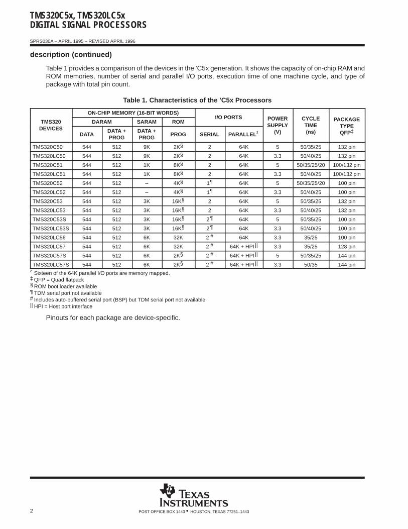
Table 1 provides a comparison of the devices in the ’C5x generation. It shows the capacity of on-chip RAM andROM memories, number of serial and parallel I/O ports, execution time of one machine cycle, and type ofpackage with total pin count.
Table 1. Characteristics of the ’C5x Processors
ON-CHIP MEMORY (16-BIT WORDS)I/O PORTS POWER CYCLE
TMS320 DARAM SARAM ROMI/O PORTS POWER
SUPPLYCYCLETIME
PACKAGETYPEDEVICES
DATADATA +PROG
DATA +PROG PROG SERIAL PARALLEL †
SUPPLY(V)
TIME(ns)
TYPEQFP‡
TMS320C50 544 512 9K 2K§ 2 64K 5 50/35/25 132 pin
TMS320LC50 544 512 9K 2K§ 2 64K 3.3 50/40/25 132 pin
TMS320C51 544 512 1K 8K§ 2 64K 5 50/35/25/20 100/132 pin
TMS320LC51 544 512 1K 8K§ 2 64K 3.3 50/40/25 100/132 pin
TMS320C52 544 512 – 4K§ 1¶ 64K 5 50/35/25/20 100 pin
TMS320LC52 544 512 – 4K§ 1¶ 64K 3.3 50/40/25 100 pin
TMS320C53 544 512 3K 16K§ 2 64K 5 50/35/25 132 pin
TMS320LC53 544 512 3K 16K§ 2 64K 3.3 50/40/25 132 pin
TMS320C53S 544 512 3K 16K§ 2¶ 64K 5 50/35/25 100 pin
TMS320LC53S 544 512 3K 16K§ 2¶ 64K 3.3 50/40/25 100 pin
TMS320LC56 544 512 6K 32K 2 # 64K 3.3 35/25 100 pin
TMS320LC57 544 512 6K 32K 2 # 64K + HPI || 3.3 35/25 128 pin
TMS320C57S 544 512 6K 2K§ 2 # 64K + HPI || 5 50/35/25 144 pin
TMS320LC57S 544 512 6K 2K§ 2 # 64K + HPI || 3.3 50/35 144 pin† Sixteen of the 64K parallel I/O ports are memory mapped.‡ QFP = Quad flatpack§ ROM boot loader available¶ TDM serial port not available# Includes auto-buffered serial port (BSP) but TDM serial port not available|| HPI = Host port interface
Pinouts for each package are device-specific.
TMS320C5x, TMS320LC5xDIGITAL SIGNAL PROCESSORS
SPRS030A – APRIL 1995 – REVISED APRIL 1996
3POST OFFICE BOX 1443 • HOUSTON, TEXAS 77251–1443
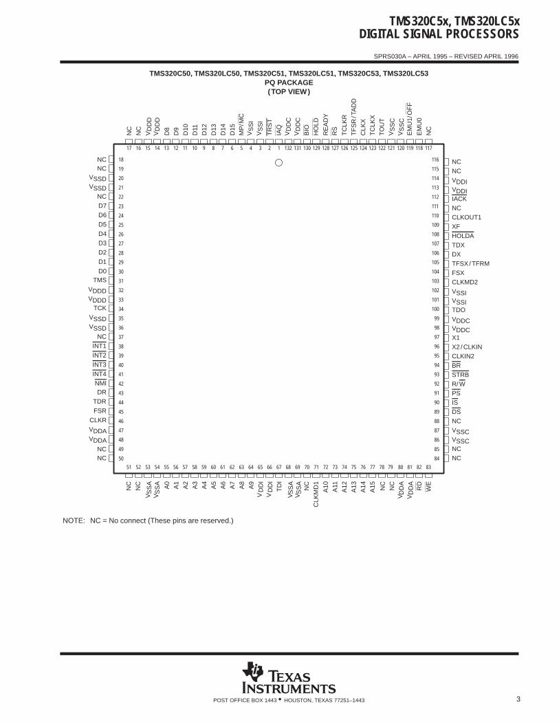
TMS320C50, TMS320LC50, TMS320C51, TMS320LC51, TMS320C53, TMS320LC53PQ PACKAGE(TOP VIEW)
WE
DD
AV D
DA
V
VSSDVSSD
D7
D6
D5
D4
D3
D2
D1
D0TMS
VDDDVDDD
TCK
VSSDVSSD
INT1
INT2
INT3
INT4
NMIDR
TDR
FSR
CLKR
VDDAVDDA VSSC
VSSC
DSIS
PS
R/ WSTRB
BR
CLKIN2X2 / CLKIN
X1
VDDC
VDDC
TDOVSSI
VSSI
FSX
TFSX/ TFRM
DXTDX
HOLDA
XFCLKOUT1
NCIACK
VDDI
VDDI
17 16 15 14 13 12 11 10 9 8 7 6 5 4 3 2 1 132 131 130 129 128 127 126 125 124 123 122 121 120 119 118 117
116
115
114
113
112
111
110
109
108
107
106
105
104
103
102
101
100
99
98
97
96
95
94
93
92
91
90
89
88
87
86
85
84
36
50
49
48
47
46
45
44
43
42
41
40
39
38
37
35
34
33
32
31
30
29
28
27
26
25
24
23
22
21
20
19
18
DD
DV
DD
DV D
8
D9
D10
D11
D12
D13
D14
D15
MP
/MC
TR
ST
IAQSS
IV
SS
IV
51 52 53 54 55 56 57 58 59 60 61 62 63 64 65 66 67 68 69 70 71 72 73 74 75 76 77 78 80 81 82 83
DD
CV
DD
CV B
IO
HO
LD
RE
AD
YR
S
TC
LKR
TF
SR
/TA
DD
CLK
X
TC
LKX
TO
UT
EM
U1/
OF
F
EM
U0
SS
CV
SS
CV
SS
AV
SS
AV
A0
A1
A2
A3
A4
A5
A6
A7
A8
TD
I
A9
CLK
MD
1
A10
A11
A12
A13
A14
A15
DD
IV
DD
IV S
SA
VS
SA
V
RD
79
NCNC
NC
NC
NCNC
NC
NC
NC
NC
NC
NC
NC
NC
NC
NC
CLKMD2
NC
NCNC
NOTE: NC = No connect (These pins are reserved.)
TMS320C5x, TMS320LC5xDIGITAL SIGNAL PROCESSORS
SPRS030A – APRIL 1995 – REVISED APRIL 1996
4 POST OFFICE BOX 1443 • HOUSTON, TEXAS 77251–1443
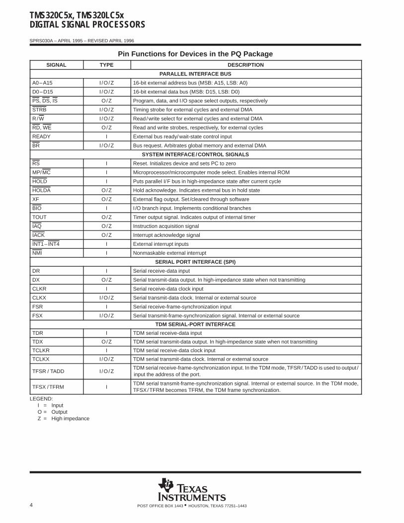
Pin Functions for Devices in the PQ PackageSIGNAL TYPE DESCRIPTION
PARALLEL INTERFACE BUS
A0–A15 I /O /Z 16-bit external address bus (MSB: A15, LSB: A0)
D0–D15 I /O /Z 16-bit external data bus (MSB: D15, LSB: D0)
PS, DS, IS O/Z Program, data, and I /O space select outputs, respectively
STRB I /O/Z Timing strobe for external cycles and external DMA
R/W I /O/Z Read/write select for external cycles and external DMA
RD, WE O/Z Read and write strobes, respectively, for external cycles
READY I External bus ready/wait-state control input
BR I /O/Z Bus request. Arbitrates global memory and external DMA
SYSTEM INTERFACE/CONTROL SIGNALS
RS I Reset. Initializes device and sets PC to zero
MP/MC I Microprocessor/microcomputer mode select. Enables internal ROM
HOLD I Puts parallel I/F bus in high-impedance state after current cycle
HOLDA O/Z Hold acknowledge. Indicates external bus in hold state
XF O/Z External flag output. Set /cleared through software
BIO I I /O branch input. Implements conditional branches
TOUT O/Z Timer output signal. Indicates output of internal timer
IAQ O/Z Instruction acquisition signal
IACK O/Z Interrupt acknowledge signal
INT1–INT4 I External interrupt inputs
NMI I Nonmaskable external interrupt
SERIAL PORT INTERFACE (SPI)
DR I Serial receive-data input
DX O/Z Serial transmit-data output. In high-impedance state when not transmitting
CLKR I Serial receive-data clock input
CLKX I /O/Z Serial transmit-data clock. Internal or external source
FSR I Serial receive-frame-synchronization input
FSX I /O/Z Serial transmit-frame-synchronization signal. Internal or external source
TDM SERIAL-PORT INTERFACE
TDR I TDM serial receive-data input
TDX O/Z TDM serial transmit-data output. In high-impedance state when not transmitting
TCLKR I TDM serial receive-data clock input
TCLKX I /O/Z TDM serial transmit-data clock. Internal or external source
TFSR / TADD I /O/ZTDM serial receive-frame-synchronization input. In the TDM mode, TFSR/TADD is used to output /input the address of the port.
TFSX /TFRM ITDM serial transmit-frame-synchronization signal. Internal or external source. In the TDM mode,TFSX/TFRM becomes TFRM, the TDM frame synchronization.
LEGEND:I = InputO = OutputZ = High impedance
TMS320C5x, TMS320LC5xDIGITAL SIGNAL PROCESSORS
SPRS030A – APRIL 1995 – REVISED APRIL 1996
5POST OFFICE BOX 1443 • HOUSTON, TEXAS 77251–1443
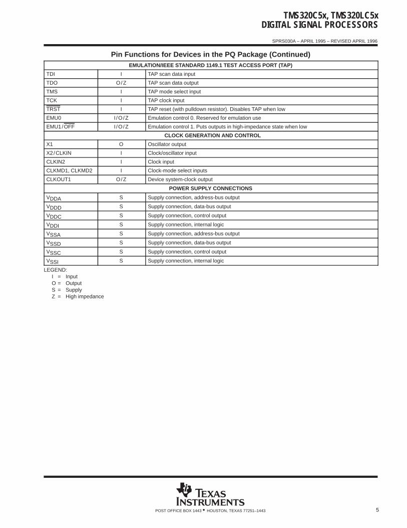
Pin Functions for Devices in the PQ Package (Continued)EMULATION/IEEE STANDARD 1149.1 TEST ACCESS PORT (TAP)
TDI I TAP scan data input
TDO O/Z TAP scan data output
TMS I TAP mode select input
TCK I TAP clock input
TRST I TAP reset (with pulldown resistor). Disables TAP when low
EMU0 I /O/Z Emulation control 0. Reserved for emulation use
EMU1/OFF I /O/Z Emulation control 1. Puts outputs in high-impedance state when low
CLOCK GENERATION AND CONTROL
X1 O Oscillator output
X2 /CLKIN I Clock/oscillator input
CLKIN2 I Clock input
CLKMD1, CLKMD2 I Clock-mode select inputs
CLKOUT1 O/Z Device system-clock output
POWER SUPPLY CONNECTIONS
VDDA S Supply connection, address-bus output
VDDD S Supply connection, data-bus output
VDDC S Supply connection, control output
VDDI S Supply connection, internal logic
VSSA S Supply connection, address-bus output
VSSD S Supply connection, data-bus output
VSSC S Supply connection, control output
VSSI S Supply connection, internal logic
LEGEND:I = InputO = OutputS = SupplyZ = High impedance
TMS320C5x, TMS320LC5xDIGITAL SIGNAL PROCESSORS
SPRS030A – APRIL 1995 – REVISED APRIL 1996
6 POST OFFICE BOX 1443 • HOUSTON, TEXAS 77251–1443
HINT
EMU0EMU1/ OFF
VSSCVSSC
TOUTBCLKX
CLKX
BFSRBCLKR
RSREADY
HOLDBIO
VDDCVDDC
IAQTRSTVSSIVSSI
MP/ MCD15D14D13D12D11D10D9D8
VDDDVDDD
HD1WE
RDHD0
HRDYVDDAA15A14A13A12
A11A10
CLKMD1VSSAVSSATDIHDS1HDS2VDDI
A9A8A7A6
A5A4
A3
A2A1
A0VSSAHCS
96
95
94
93
92
91
90
89
88
87
86
85
84
83
82
81
80
79
78
77
76
75
74
73
72
71
70
69
68
67
66
65
1
2
3
4
5
6
7
8
9
10
11
12
13
14
15
16
17
18
19
20
21
22
23
24
25
26
27
28
29
30
31
32
128
33
127 126 125 124 123 122 121 120 119 118 117 116 115 114 113 112 111 110 109 108 107 106 105 104 103 102 101 100 99 98 97
34 35 36 37 38 39 40 41 42 43 44 45 46 47 48 49 50 51 52 53 54 55 56 57 58 59 60 61 62 63 64
SS
DV
SS
DV
D7
VD
6C
LKO
UT
1D
5X
FD
4H
OLD
AD
3B
DX
D2
DX
D1
HD
7D
0B
FS
X
TM
SH
D6
DD
DD
DD
TC
K
CLK
MD
2
SS
DS
SD
INT
1IN
T2
TD
O
INT
3IN
T4
X1
NM
I
X2/
CLK
IN
CLK
MD
3
ST
RB
R/W
DR
BD
R
HD
3
FS
RIS
CLK
R
PS
DD
AH
D2
DD
A
HA
S
DD
CD
DI
DD
I
V V V V V V V V
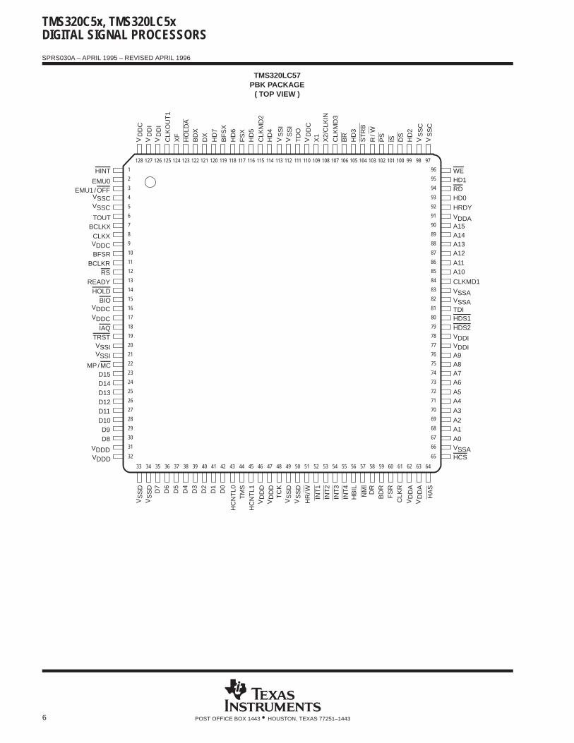
TMS320LC57PBK PACKAGE
( TOP VIEW )
FS
XH
D5
HD
4V
SS
IV
SS
I
VD
DC
BR
DS
V VS
SC
SS
C
VDDIH
BIL
HR
/W
HC
NT
L0
HC
NT
L1VDDC
TMS320C5x, TMS320LC5xDIGITAL SIGNAL PROCESSORS
SPRS030A – APRIL 1995 – REVISED APRIL 1996
7POST OFFICE BOX 1443 • HOUSTON, TEXAS 77251–1443
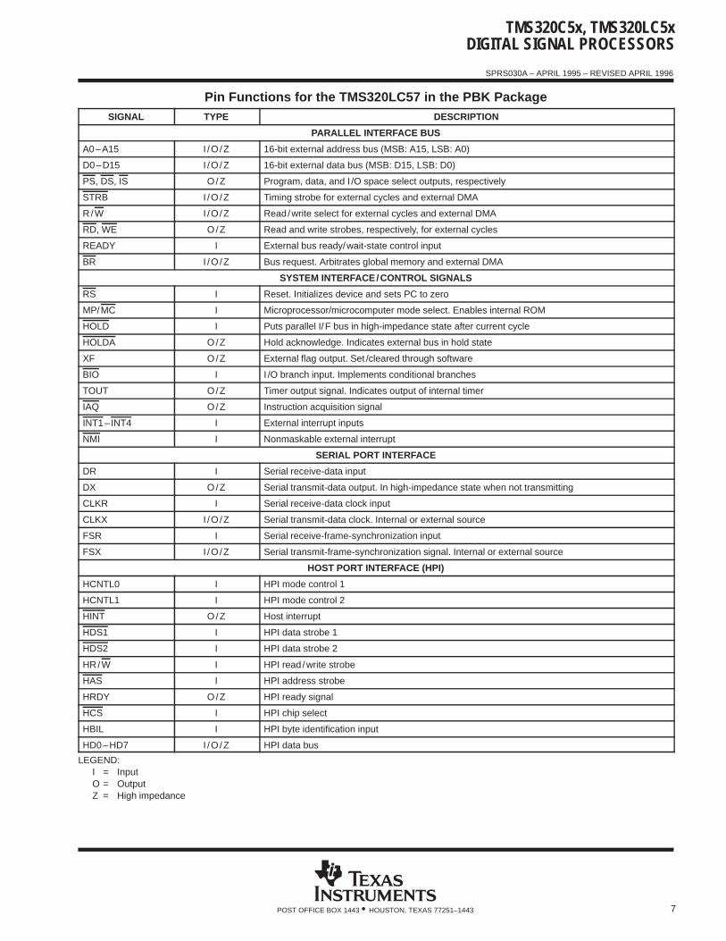
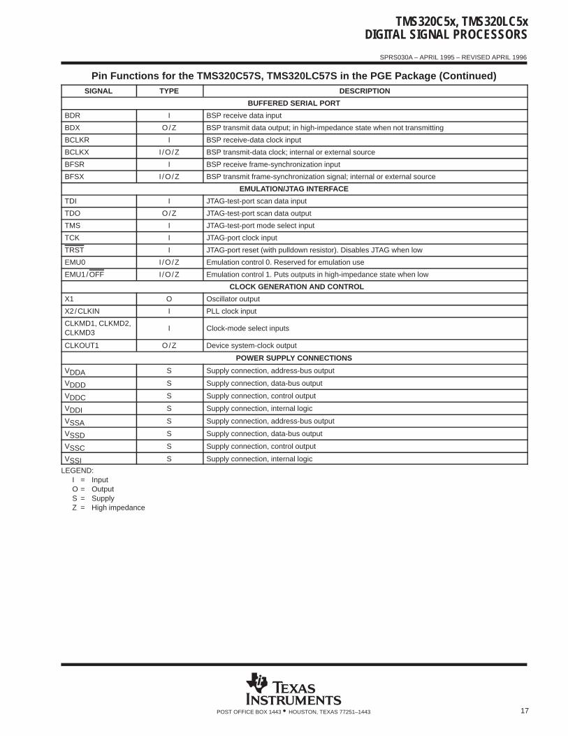
Pin Functions for the TMS320LC57 in the PBK PackageSIGNAL TYPE DESCRIPTION
PARALLEL INTERFACE BUS
A0–A15 I /O /Z 16-bit external address bus (MSB: A15, LSB: A0)
D0–D15 I /O /Z 16-bit external data bus (MSB: D15, LSB: D0)
PS, DS, IS O/Z Program, data, and I /O space select outputs, respectively
STRB I /O/Z Timing strobe for external cycles and external DMA
R/W I /O/Z Read/write select for external cycles and external DMA
RD, WE O/Z Read and write strobes, respectively, for external cycles
READY I External bus ready/wait-state control input
BR I /O/Z Bus request. Arbitrates global memory and external DMA
SYSTEM INTERFACE/CONTROL SIGNALS
RS I Reset. Initializes device and sets PC to zero
MP/MC I Microprocessor/microcomputer mode select. Enables internal ROM
HOLD I Puts parallel I/F bus in high-impedance state after current cycle
HOLDA O/Z Hold acknowledge. Indicates external bus in hold state
XF O/Z External flag output. Set /cleared through software
BIO I I /O branch input. Implements conditional branches
TOUT O/Z Timer output signal. Indicates output of internal timer
IAQ O/Z Instruction acquisition signal
INT1–INT4 I External interrupt inputs
NMI I Nonmaskable external interrupt
SERIAL PORT INTERFACE
DR I Serial receive-data input
DX O/Z Serial transmit-data output. In high-impedance state when not transmitting
CLKR I Serial receive-data clock input
CLKX I /O/Z Serial transmit-data clock. Internal or external source
FSR I Serial receive-frame-synchronization input
FSX I /O/Z Serial transmit-frame-synchronization signal. Internal or external source
HOST PORT INTERFACE (HPI)
HCNTL0 I HPI mode control 1
HCNTL1 I HPI mode control 2
HINT O/Z Host interrupt
HDS1 I HPI data strobe 1
HDS2 I HPI data strobe 2
HR/W I HPI read /write strobe
HAS I HPI address strobe
HRDY O/Z HPI ready signal
HCS I HPI chip select
HBIL I HPI byte identification input
HD0–HD7 I /O/Z HPI data bus
LEGEND:I = InputO = OutputZ = High impedance
TMS320C5x, TMS320LC5xDIGITAL SIGNAL PROCESSORS
SPRS030A – APRIL 1995 – REVISED APRIL 1996
8 POST OFFICE BOX 1443 • HOUSTON, TEXAS 77251–1443
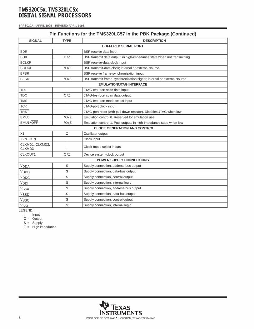
Pin Functions for the TMS320LC57 in the PBK Package (Continued)SIGNAL TYPE DESCRIPTION
BUFFERED SERIAL PORT
BDR I BSP receive data input
BDX O/Z BSP transmit data output; in high-impedance state when not transmitting
BCLKR I BSP receive-data clock input
BCLKX I /O/Z BSP transmit-data clock; internal or external source
BFSR I BSP receive frame-synchronization input
BFSX I /O/Z BSP transmit frame-synchronization signal; internal or external source
EMULATION/JTAG INTERFACE
TDI I JTAG-test-port scan data input
TDO O/Z JTAG-test-port scan data output
TMS I JTAG-test-port mode select input
TCK I JTAG-port clock input
TRST I JTAG-port reset (with pull-down resistor). Disables JTAG when low
EMU0 I /O/Z Emulation control 0. Reserved for emulation use
EMU1/OFF I /O/Z Emulation control 1. Puts outputs in high-impedance state when low
CLOCK GENERATION AND CONTROL
X1 O Oscillator output
X2 /CLKIN I Clock input
CLKMD1, CLKMD2,CLKMD3
I Clock-mode select inputs
CLKOUT1 O/Z Device system-clock output
POWER SUPPLY CONNECTIONS
VDDA S Supply connection, address-bus output
VDDD S Supply connection, data-bus output
VDDC S Supply connection, control output
VDDI S Supply connection, internal logic
VSSA S Supply connection, address-bus output
VSSD S Supply connection, data-bus output
VSSC S Supply connection, control output
VSSI S Supply connection, internal logic
LEGEND:I = InputO = OutputS = SupplyZ = High impedance
TMS320C5x, TMS320LC5xDIGITAL SIGNAL PROCESSORS
SPRS030A – APRIL 1995 – REVISED APRIL 1996
9POST OFFICE BOX 1443 • HOUSTON, TEXAS 77251–1443
INT
3IN
T2
INT
1
HO
LDA
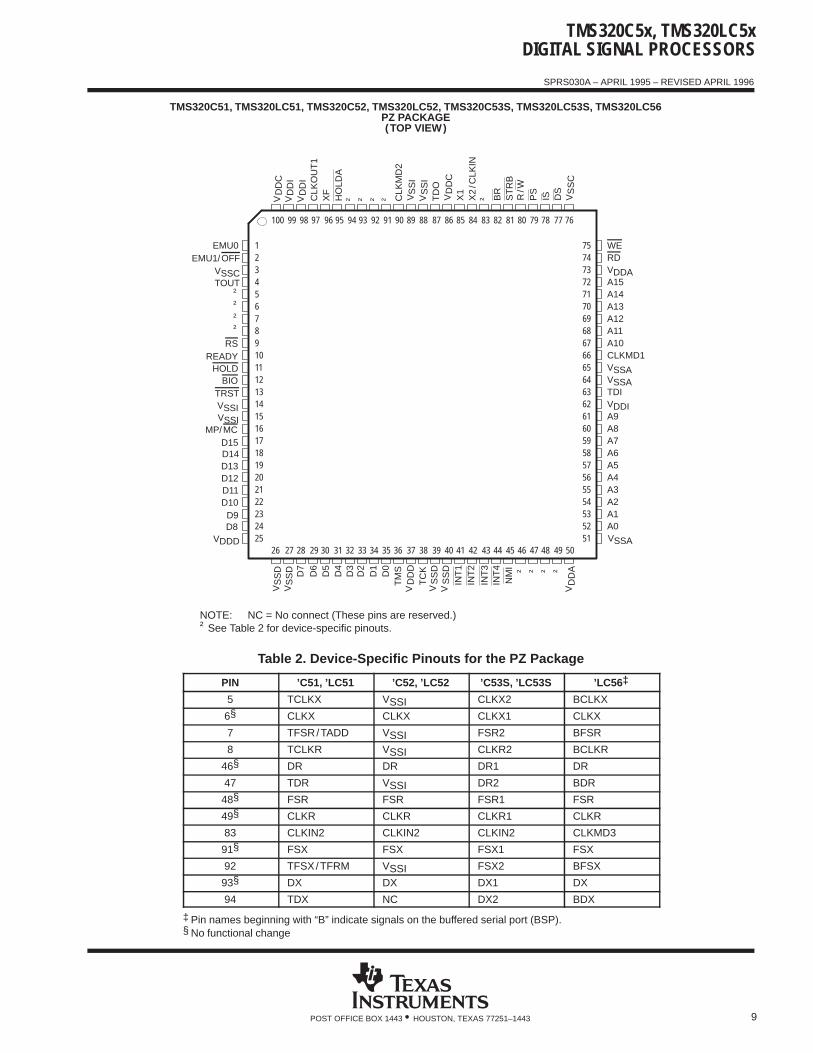
TMS320C51, TMS320LC51, TMS320C52, TMS320LC52, TMS320C53S, TMS320LC53S, TMS320LC56PZ PACKAGE(TOP VIEW)
EMU1/OFFVSSC
RSREADY
HOLDBIO
TRST
VSSIMP/MC
D15D14
D12D11D10
D9D8
VDDD
18
25242322212019
1716151413121110987654321EMU0
TOUT
D13
VSSI
58
51525354555657
5960616263646566676869707172737475
RDVDDAA15A14A13A12A11A10CLKMD1VSSAVSSA
VDDIA9A8A7
A5A4A3A2A1
WE
A6
TDI
A0
100 99 98 97 96 95 94 93 92 91 90 89 88 87 86 85 84 83 82 81 80 79 78 77 76
DD
CV C
LKO
UT
1X
F
† † CLK
MD
2
TD
O
† BR
R/W
DS
X1D
DI
V
DD
IV
SS
IV
SS
IV
DD
CV
SS
CVS
TR
B
PS
IS26 27 28 29 30 31 32 33 34 35 36 37 38 39 40 41 42 43 44 45 46 47 48 49 50
SS
DV
D7
D6
D3
D2
D1
D0
TM
S
TC
K
SS
DV
DD
DV
D5
D4
INT
4N
MI † ††
† X2
/CLK
IN
VSSA
††††
†
†
DD
AV
SS
DV
SS
DV
† See Table 2 for device-specific pinouts.NOTE: NC = No connect (These pins are reserved.)
Table 2. Device-Specific Pinouts for the PZ Package
PIN ’C51, ’LC51 ’C52, ’LC52 ’C53S, ’LC53S ’LC56‡
5 TCLKX VSSI CLKX2 BCLKX
6§ CLKX CLKX CLKX1 CLKX
7 TFSR/TADD VSSI FSR2 BFSR
8 TCLKR VSSI CLKR2 BCLKR
46§ DR DR DR1 DR
47 TDR VSSI DR2 BDR
48§ FSR FSR FSR1 FSR
49§ CLKR CLKR CLKR1 CLKR
83 CLKIN2 CLKIN2 CLKIN2 CLKMD3
91§ FSX FSX FSX1 FSX
92 TFSX/TFRM VSSI FSX2 BFSX
93§ DX DX DX1 DX
94 TDX NC DX2 BDX
‡ Pin names beginning with “B” indicate signals on the buffered serial port (BSP).§ No functional change
TMS320C5x, TMS320LC5xDIGITAL SIGNAL PROCESSORS
SPRS030A – APRIL 1995 – REVISED APRIL 1996
10 POST OFFICE BOX 1443 • HOUSTON, TEXAS 77251–1443
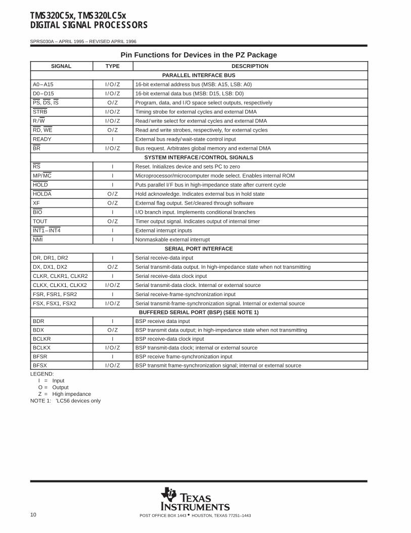
Pin Functions for Devices in the PZ PackageSIGNAL TYPE DESCRIPTION
PARALLEL INTERFACE BUS
A0–A15 I /O /Z 16-bit external address bus (MSB: A15, LSB: A0)
D0–D15 I /O /Z 16-bit external data bus (MSB: D15, LSB: D0)
PS, DS, IS O/Z Program, data, and I /O space select outputs, respectively
STRB I /O/Z Timing strobe for external cycles and external DMA
R/W I /O/Z Read/write select for external cycles and external DMA
RD, WE O/Z Read and write strobes, respectively, for external cycles
READY I External bus ready/wait-state control input
BR I /O/Z Bus request. Arbitrates global memory and external DMA
SYSTEM INTERFACE/CONTROL SIGNALS
RS I Reset. Initializes device and sets PC to zero
MP/MC I Microprocessor/microcomputer mode select. Enables internal ROM
HOLD I Puts parallel I/F bus in high-impedance state after current cycle
HOLDA O/Z Hold acknowledge. Indicates external bus in hold state
XF O/Z External flag output. Set /cleared through software
BIO I I /O branch input. Implements conditional branches
TOUT O/Z Timer output signal. Indicates output of internal timer
INT1–INT4 I External interrupt inputs
NMI I Nonmaskable external interrupt
SERIAL PORT INTERFACE
DR, DR1, DR2 I Serial receive-data input
DX, DX1, DX2 O/Z Serial transmit-data output. In high-impedance state when not transmitting
CLKR, CLKR1, CLKR2 I Serial receive-data clock input
CLKX, CLKX1, CLKX2 I /O/Z Serial transmit-data clock. Internal or external source
FSR, FSR1, FSR2 I Serial receive-frame-synchronization input
FSX, FSX1, FSX2 I /O/Z Serial transmit-frame-synchronization signal. Internal or external source
BUFFERED SERIAL PORT (BSP) (SEE NOTE 1)
BDR I BSP receive data input
BDX O/Z BSP transmit data output; in high-impedance state when not transmitting
BCLKR I BSP receive-data clock input
BCLKX I /O/Z BSP transmit-data clock; internal or external source
BFSR I BSP receive frame-synchronization input
BFSX I /O/Z BSP transmit frame-synchronization signal; internal or external source
LEGEND:I = InputO = OutputZ = High impedance
NOTE 1: ’LC56 devices only
TMS320C5x, TMS320LC5xDIGITAL SIGNAL PROCESSORS
SPRS030A – APRIL 1995 – REVISED APRIL 1996
11POST OFFICE BOX 1443 • HOUSTON, TEXAS 77251–1443
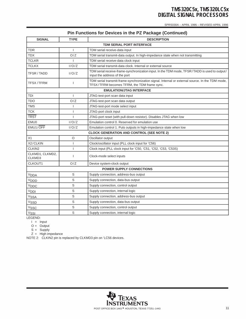
Pin Functions for Devices in the PZ Package (Continued)SIGNAL TYPE DESCRIPTION
TDM SERIAL PORT INTERFACE
TDR I TDM serial receive-data input
TDX O/Z TDM serial transmit-data output. In high-impedance state when not transmitting
TCLKR I TDM serial receive-data clock input
TCLKX I /O/Z TDM serial transmit-data clock. Internal or external source
TFSR / TADD I /O/ZTDM serial receive-frame-synchronization input. In the TDM mode, TFSR/TADD is used to output /input the address of the port
TFSX /TFRM ITDM serial transmit-frame-synchronization signal. Internal or external source. In the TDM mode,TFSX/TFRM becomes TFRM, the TDM frame sync.
EMULATION/JTAG INTERFACE
TDI I JTAG-test-port scan data input
TDO O/Z JTAG-test-port scan data output
TMS I JTAG-test-port mode select input
TCK I JTAG-port clock input
TRST I JTAG-port reset (with pull-down resistor). Disables JTAG when low
EMU0 I /O/Z Emulation control 0. Reserved for emulation use
EMU1/OFF I /O/Z Emulation control 1. Puts outputs in high-impedance state when low
CLOCK GENERATION AND CONTROL (SEE NOTE 2)
X1 O Oscillator output
X2 /CLKIN I Clock/oscillator input (PLL clock input for ’C56)
CLKIN2 I Clock input (PLL clock input for ’C50, ’C51, ’C52, ’C53, ’C53S)
CLKMD1, CLKMD2,CLKMD3
I Clock-mode select inputs
CLKOUT1 O/Z Device system-clock output
POWER SUPPLY CONNECTIONS
VDDA S Supply connection, address-bus output
VDDD S Supply connection, data-bus output
VDDC S Supply connection, control output
VDDI S Supply connection, internal logic
VSSA S Supply connection, address-bus output
VSSD S Supply connection, data-bus output
VSSC S Supply connection, control output
VSSI S Supply connection, internal logic
LEGEND:I = InputO = OutputS = SupplyZ = High impedance
NOTE 2: CLKIN2 pin is replaced by CLKMD3 pin on ’LC56 devices.
TMS320C5x, TMS320LC5xDIGITAL SIGNAL PROCESSORS
SPRS030A – APRIL 1995 – REVISED APRIL 1996
12 POST OFFICE BOX 1443 • HOUSTON, TEXAS 77251–1443
D8
VDDDVSSDVSSD
D7
D6
D5
D4
D3
D2
D1
D0
TMS
VDDDVDDD
TCK
VSSDVSSD
INT1
INT2
INT3
INT4
NMI
DR
VSSIFSR
CLKR
VDDAVSSA
A0
100
31 32 33 34 35 36 37 38 39 40 41 42 43 44 45 46 47 48 49 50
99 98 97 96 95 94 93 92 91 90 89 88 87 86 85 84 83 82 81
SS
AA2
A3
A4
A5
A1
A7
A8
A9
A6
DD
IT
DI
CLK
MD
1
A11
A12
A13
A14
A10
A15
MP
/MC
D10
D11
D12
D13
D9
D14
V TR
ST
CLK
X
HO
LDR
EA
DY
BIO
RS
V V TO
UT
VVD15
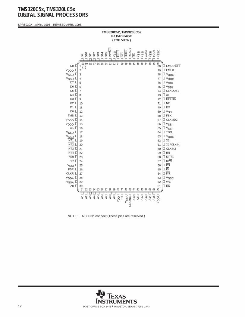
TMS320C52, TMS320LC52PJ PACKAGE(TOP VIEW)
DD
A
SS
I
SS
IS
SI
SS
C
SS
I
EMU1/OFF
EMU0
VDDCVDDCVDDIVDDICLKOUT1
XF
HOLDA
NC
DX
VSSIFSX
CLKMD2
VSSIVSSITDO
VDDCX1
X2 / CLKIN
CLKIN2
BR
STRB
R/ W
PS
IS
DS
VSSCWE
RD
V V V
1
2
3
4
5
6
7
8
9
10
11
12
13
14
15
16
17
18
19
20
21
22
23
24
25
26
27
28
29
30
80
79
78
77
76
75
74
73
72
71
70
69
68
67
66
65
64
63
62
61
60
59
58
57
56
55
54
53
52
51
NOTE: NC = No connect (These pins are reserved.)
TMS320C5x, TMS320LC5xDIGITAL SIGNAL PROCESSORS
SPRS030A – APRIL 1995 – REVISED APRIL 1996
13POST OFFICE BOX 1443 • HOUSTON, TEXAS 77251–1443
Pin Functions for the TMS320C52, TMS320LC52 in the PJ PackageSIGNAL TYPE DESCRIPTION
PARALLEL INTERFACE BUS
A0–A15 I /O /Z 16-bit external address bus (MSB: A15, LSB: A0)
D0–D15 I /O /Z 16-bit external data bus (MSB: D15, LSB: D0)
PS, DS, IS O/Z Program, data, and I /O space select outputs, respectively
STRB I /O/Z Timing strobe for external cycles and external DMA
R/W I /O/Z Read/write select for external cycles and external DMA
RD, WE O/Z Read and write strobes, respectively, for external cycles
READY I External bus ready/wait-state control input
BR I /O/Z Bus request. Arbitrates global memory and external DMA
SYSTEM INTERFACE/CONTROL SIGNALS
RS I Reset. Initializes device and sets PC to zero
MP/MC I Microprocessor/microcomputer mode select. Enables internal ROM
HOLD I Puts parallel I/F bus in high-impedance state after current cycle
HOLDA O/Z Hold acknowledge. Indicates external bus in hold state
XF O/Z External flag output. Set /cleared through software
BIO I I /O branch input. Implements conditional branches
TOUT O/Z Timer output signal. Indicates output of internal timer
INT1–INT4 I External interrupt inputs
NMI I Nonmaskable external interrupt
SERIAL PORT INTERFACE
DR I Serial receive-data input
DX O/Z Serial transmit-data output. In high-impedance state when not transmitting
CLKR I Serial receive-data clock input
CLKX I /O/Z Serial transmit-data clock. Internal or external source
FSR I Serial receive-frame-synchronization input
FSX I /O/Z Serial transmit-frame-synchronization signal. Internal or external source
EMULATION/JTAG INTERFACE
TDI I JTAG-test-port scan data input
TDO O/Z JTAG-test-port scan data output
TMS I JTAG-test-port mode select input
TCK I JTAG-port clock input
TRST I JTAG-port reset (with pulldown resistor). Disables JTAG when low
EMU0 I /O/Z Emulation control 0. Reserved for emulation use
EMU1/OFF I /O/Z Emulation control 1. Puts outputs in high-impedance state when low
LEGEND:I = InputO = OutputZ = High impedance
TMS320C5x, TMS320LC5xDIGITAL SIGNAL PROCESSORS
SPRS030A – APRIL 1995 – REVISED APRIL 1996
14 POST OFFICE BOX 1443 • HOUSTON, TEXAS 77251–1443
Pin Functions for the TMS320C52, TMS320LC52 in the PJ Package (Continued)SIGNAL TYPE DESCRIPTION
CLOCK GENERATION AND CONTROL
X1 O Oscillator output
X2 /CLKIN I Clock/oscillator input
CLKIN2 I Clock input (PLL clock input for ’C52, ’LC52)
CLKMD1, CLKMD2 I Clock-mode select inputs
CLKOUT1 O/Z Device system-clock output
POWER SUPPLY CONNECTIONS
VDDA S Supply connection, address-bus output
VDDD S Supply connection, data-bus output
VDDC S Supply connection, control output
VDDI S Supply connection, internal logic
VSSA S Supply connection, address-bus output
VSSD S Supply connection, data-bus output
VSSC S Supply connection, control output
VSSI S Supply connection, internal logic
LEGEND:I = InputO = OutputS = Supply
TMS320C5x, TMS320LC5xDIGITAL SIGNAL PROCESSORS
SPRS030A – APRIL 1995 – REVISED APRIL 1996
15POST OFFICE BOX 1443 • HOUSTON, TEXAS 77251–1443
TMS320C57S, TMS320LC57SPGE PACKAGE
(TOP VIEW)
TD
O
WEHD1RDHD0HRDYVDDAA15NCA14A13A12NCA11A10CLKMD1VSSAVSSATDIHDS1HDS2VDDIVDDIA9A8A7NCA6A5A4A3NCA2A1A0VSSAHCS
HINTEMU0
NCEMU1/OFF
VSSCVSSCTOUT
BCLKXCLKXVDDCBFSR
BCLKRRS
READYHOLD
NCBIO
VDDCVDDC
IAQTRSTVSSIVSSI
MP/MCD15D14D13NC
D12D11D10D9NCD8
VDDDVDDD
144
143
142
CLK
OU
T1
141
XF
140
139
BD
X13
8
137
136
BF
SX
135
134
133
HD
513
2
CLK
MD
213
1
130
129
128
127
126
125
X2/
CLK
IN
124
CLK
MD
3
123
122
HD
3
121
ST
RB
120
119
PS
118
117
116
115
114
113
112
37 38 39 40 41 42 43 44 45 46 47 48 49 50 51 52 53 54 55 56 57 58 59 60 61 62 63 64 65 66 67 68 69
1
2
3
4
5
6
7
8
9
10
11
12
13
14
15
16
17
18
19
20
21
22
23
24
25
26
27
28
29
30
31
32
33
34
35
36
108
107
106
105
104
103
102
101
100
99
98
97
96
95
94
93
92
91
90
89
88
87
86
85
84
83
82
81
80
79
78
77
76
75
74
73
D7
D6
D5
D3
D2
D1
HC
NT
L0T
MS
NM
I
HR
/W
INT
2IN
T3
INT
4
DR
BD
RF
SR
HA
S
HC
NT
L1
111
NC
110
109
70 71 72
NC
TC
K
HD
6
DX
V SS
I
HD
4
V DD
C
DD
DV C
LKR
DD
AV
HB
IL
SS
DV
D4
D0
INT
1
NC
V DD
CV D
DI
V HO
LDA
HD
7
FS
X
V SS
I
X1
BR
R/W
IS DS
HD
2V S
SC
V SS
C
NC
NC
NC
SS
DV
DD
IS
SD
V DD
DV
SS
DV D
DA
V
NOTE: NC = No connect (These pins are reserved.)
NC
NC
AD
VA
NC
E IN
FO
RM
ATIO
N
TMS320C5x, TMS320LC5xDIGITAL SIGNAL PROCESSORS
SPRS030A – APRIL 1995 – REVISED APRIL 1996
16 POST OFFICE BOX 1443 • HOUSTON, TEXAS 77251–1443
Pin Functions for the TMS320C57S, TMS320LC57S in the PGE PackageSIGNAL TYPE DESCRIPTION
PARALLEL INTERFACE BUS
A0–A15 I /O /Z 16-bit external address bus (MSB: A15, LSB: A0)
D0–D15 I /O /Z 16-bit external data bus (MSB: D15, LSB: D0)
PS, DS, IS O/Z Program, data, and I /O space select outputs, respectively
STRB I /O/Z Timing strobe for external cycles and external DMA
R/W I /O/Z Read/write select for external cycles and external DMA
RD, WE O/Z Read and write strobes, respectively, for external cycles
READY I External bus ready/wait-state control input
BR I /O/Z Bus request. Arbitrates global memory and external DMA
SYSTEM INTERFACE/CONTROL SIGNALS
RS I Reset. Initializes device and sets PC to zero
MP/MC I Microprocessor/microcomputer mode select. Enables internal ROM
HOLD I Puts parallel I/F bus in high-impedance state after current cycle
HOLDA O/Z Hold acknowledge. Indicates external bus in hold state
XF O/Z External flag output. Set /cleared through software
BIO I I /O branch input. Implements conditional branches
TOUT O/Z Timer output signal. Indicates output of internal timer
IAQ O/Z Instruction acquisition signal
INT1–INT4 I External interrupt inputs
NMI I Nonmaskable external interrupt
SERIAL PORT INTERFACE (SPI)
DR I Serial receive-data input
DX O/Z Serial transmit-data output. In high-impedance state when not transmitting
CLKR I Serial receive-data clock input
CLKX I /O/Z Serial transmit-data clock. Internal or external source
FSR I Serial receive-frame-synchronization input
FSX I /O/Z Serial transmit-frame-synchronization signal. Internal or external source
HOST PORT INTERFACE (HPI)
HCNTL0 I HPI mode control 1
HCNTL1 I HPI mode control 2
HINT O/Z Host interrupt
HDS1 I HPI data strobe 1
HDS2 I HPI data strobe 2
HR/W I HPI read /write strobe
HAS I HPI address strobe
HRDY O/Z HPI ready signal
HCS I HPI chip select
HBIL I HPI byte identification input
HD0–HD7 I /O/Z HPI data bus
LEGEND:I = InputO = OutputZ = High impedance
TMS320C5x, TMS320LC5xDIGITAL SIGNAL PROCESSORS
SPRS030A – APRIL 1995 – REVISED APRIL 1996
17POST OFFICE BOX 1443 • HOUSTON, TEXAS 77251–1443
Pin Functions for the TMS320C57S, TMS320LC57S in the PGE Package (Continued)SIGNAL TYPE DESCRIPTION
BUFFERED SERIAL PORT
BDR I BSP receive data input
BDX O/Z BSP transmit data output; in high-impedance state when not transmitting
BCLKR I BSP receive-data clock input
BCLKX I /O/Z BSP transmit-data clock; internal or external source
BFSR I BSP receive frame-synchronization input
BFSX I /O/Z BSP transmit frame-synchronization signal; internal or external source
EMULATION/JTAG INTERFACE
TDI I JTAG-test-port scan data input
TDO O/Z JTAG-test-port scan data output
TMS I JTAG-test-port mode select input
TCK I JTAG-port clock input
TRST I JTAG-port reset (with pulldown resistor). Disables JTAG when low
EMU0 I /O/Z Emulation control 0. Reserved for emulation use
EMU1/OFF I /O/Z Emulation control 1. Puts outputs in high-impedance state when low
CLOCK GENERATION AND CONTROL
X1 O Oscillator output
X2 /CLKIN I PLL clock input
CLKMD1, CLKMD2,CLKMD3
I Clock-mode select inputs
CLKOUT1 O/Z Device system-clock output
POWER SUPPLY CONNECTIONS
VDDA S Supply connection, address-bus output
VDDD S Supply connection, data-bus output
VDDC S Supply connection, control output
VDDI S Supply connection, internal logic
VSSA S Supply connection, address-bus output
VSSD S Supply connection, data-bus output
VSSC S Supply connection, control output
VSSI S Supply connection, internal logic
LEGEND:I = InputO = OutputS = SupplyZ = High impedance
TMS320C5x, TMS320LC5xDIGITAL SIGNAL PROCESSORS
SPRS030A – APRIL 1995 – REVISED APRIL 1996
18 POST OFFICE BOX 1443 • HOUSTON, TEXAS 77251–1443
architecture
The ’C5x’s advanced Harvard-type architecture maximizes the processing power by maintaining two separatememory bus structures, program and data, for full-speed execution. Instructions support data transfers betweenthe two spaces. This architecture permits coefficients stored in program memory to be read into the RAM,eliminating the need for a separate coefficient ROM. The ’C5x architecture also makes available immediateinstructions and subroutines based on computed values. Increased throughput on the ’C5x for many DSPapplications is accomplished using single-cycle multiply/accumulate instructions with a data-move option, upto eight auxiliary registers with a dedicated arithmetic unit, a parallel logic unit, and faster I/O necessary fordata-intensive signal processing. The architectural design emphasizes overall speed, communication, andflexibility in processor configuration. Control signals and instructions provide floating-point support,block-memory transfers, communication to slower off-chip devices, and multiprocessing implementationsas shown in the functional block diagram.
Table 3 explains the symbols that are used in the functional block diagram.
Table 3. Symbols Used in Functional Block Diagram
SYMBOL DESCRIPTION SYMBOL DESCRIPTION
ABU Auto-buffering unit IFR Interrupt-flag register
ACCB Accumulator buffer IMR Interrupt-mask register
ACCH Accumulator high INDX Indirect-addressing-index register
ACCL Accumulator low IR Instruction register
ALU Arithmetic logic unit MCS Microcall stack
ARAU Auxiliary-register arithmetic unit MUX Multiplexer
ARB Auxiliary-register pointer buffer PAER Block-repeat-address end register
ARCR Auxiliary-register compare register PASR Block-repeat-address start register
ARP Auxiliary-register pointer PC Program counter
ARR Address-receive register (ABU) PFC Prefetch counter
AR0–AR7 Auxiliary registers PLU Parallel logic unit
AXR Address-transmit register (ABU) PMST Processor-mode-status register
BKR Receive-buffer-size register (ABU) PRD Timer-period register
BKX Transmit-buffer-size register (ABU) PREG Product register
BMAR Block-move-address register RPTC Repeat-counter register
BRCR Block-repeat-counter register SARAM Single-access RAM
BSP Buffered serial port SFL Left shifter
C Carry bit SFR Right shifter
CBER1 Circular buffer 1 end address SPC Serial-port interface-control register
CBER2 Circular buffer 2 end address ST0,ST1 Status registers
CBSR1 Circular buffer 1 start address TCSR TDM channel-select register
CBSR2 Circular buffer 2 start address TCR Timer-control register
DARAM Dual-access RAM TDM Time-division-multiplexed serial port
DBMR Dynamic bit manipulation register TDXR TDM data transmit register
DP Data memory page pointer TIM Timer-count register
DRR Serial-port data receive register TRAD TDM received-address register
DXR Serial-port data transmit register TRCV TDM data-receive register
GREG Global memory allocation register TREG0 Temporary register for multiplication
HPI Host port interface TREG1 Temporary register for dynamic shift count
HPIAH HPI-address register (high bytes) TREG2 Temporary register used as bit pointer in dynamic-bit test
HPIAL HPI-address register (low bytes) TRTA TDM receive-/transmit-address register
HPICH HPI-control register (high bytes) TSPC TDM serial-port-control register
HPICL HPI-control register (low bytes)
TMS320C5x, TMS320LC5xDIGITAL SIGNAL PROCESSORS
SPRS030A – APRIL 1995 – REVISED APRIL 1996
19POST OFFICE BOX 1443 • HOUSTON, TEXAS 77251–1443
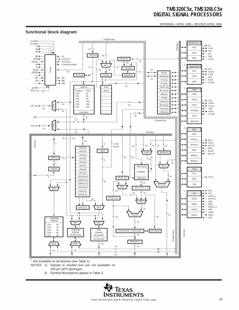
functional block diagram
32
16
Data Bus
Program Bus
16
16
Shifter(0–7)
D15–D0
RBIT
A15–A0
16
16
16
16
DBMR(16)
MUX
16 16
32
ACCB(32)
32
ACCL(16)ACCH(16)C
32
ALU(32)
32
SFR(0–16)
32
MUX
MUX
SFL(0–16)
16
MUX
PREG(32)
Multiplier
TREG0(16)
MUX
16
1616
MUX
B1 (512x16)
B2 (32x16)DARAM
B0 (512x16)DARAM
MUX
from IR7 LSB
MUX
DP(9)
9
9
MUX
16
’C50 9K’C51 1K’C53 3K’C56 6K’C57 6K
SARAM
16
ARAU(16)
16
MUX
3
3
3
3
ARB(3)
ARP(3)
Program Bus
16
16
1616
CBSR2(16)
CBSR1(16)
AR7(16)
AR6(16)
AR5(16)
AR3(16)
AR2(16)
AR1(16)
AR0(16)
ARCR(16)
INDX(16)
HDS(1–1)
HRDY
HASHR/W
HINT
HPI
HPICL
HD7HD0
HBILHCNTL0HCNTL1
HCSHPIAL
HPICH
HPIAH
TOUT
TCR
PRD
TIM
Timer
BDX
BCLKXBDR
BCLKRBFSR
DFSX
DXR
AXR(11)
BKX(11)
DRR
ARR(11)
BKR(11)
BSP
TDM
TCSR(8)
TRTA
TRAD(16)
TDRTCLKXTFRM
TADDTCLKR
TRCV
TDXR
TSPC
TDX
CLKX2FSX2
DX2
FSR2CLKR2
DR2
SPC
DXR
DRR
Serial Port 2
CLKRFSRDRFSXCLKXDX
DRR
DXR
SPC
Serial Port 1
16
16
TREG2(4)
TREG1(5)
BRCR(16)
GREG(16)
IFR(16)
IMR(16)
RPTC(16)
PMST(16)
ST1(16)
ST0(16)
BMAR(16)
IR(16)
16
16
16
16
16
PFC(16)
MCS(16)
Instruction
Address
32K’C5732K’C5616K’C534K’C528K’C512K’C50ROMProgram
16
16
16
16
16
PASR(16)
Compare
PAER(16)
(8x16)
Stack
PC(16)
16
MUX
NMIWERD
16
CLKIN2/CLKMD3X2/CLKINCLKOUT1X1
4INT(1–4)MP/MC
IACKRS
HOLDAHOLD
XFBR
READYSTRB
RW
PSDSIS
CLKMD2CLKMD1
Con
trol
Dat
a B
us
Pro
gram
Bus
Dat
a B
us
Dat
a B
us
CBER2(16)
CBER1(16)
AR4(16)
16
BOIAQ
†
†
†
†
MU
XM
UX
Data/Prog
Data/Prog
16
SFL (–6, 0, 1, 4)
PLU (16)
16
Data
32
16
16
16
16
16
16
32
32
16
† Not available on all devices (see Table 1).NOTES: A. Signals in shaded text are not available on
100-pin QFP packages.B. Symbol descriptions appear in Table 3.
TMS320C5x, TMS320LC5xDIGITAL SIGNAL PROCESSORS
SPRS030A – APRIL 1995 – REVISED APRIL 1996
20 POST OFFICE BOX 1443 • HOUSTON, TEXAS 77251–1443
32-bit ALU/accumulator
The 32-bit ALU and accumulator implement a wide range of arithmetic and logical functions, the majority ofwhich execute in a single cycle. The ALU is a general-purpose arithmetic/logic unit that operates on 16-bit wordstaken from data memory or derived from immediate instructions. In addition to the usual arithmetic instructions,the ALU can perform Boolean operations, facilitating the bit manipulation ability required of a high-speedcontroller. One input to the ALU always is supplied by the accumulator, and the other input can be furnishedfrom the product register (PREG) of the multiplier, the accumulator buffer (ACCB), or the output of the scalingshifter [which has been read from data memory or from the accumulator (ACC)]. After the ALU performs thearithmetic or logical operation, the result is stored in the ACC where additional operations, such as shifting, canbe performed. Data input to the ALU can be scaled by the scaling shifter. The 32-bit ACC is split into two 16-bitsegments for storage in data memory. Shifters at the output of the ACC provide a left shift of 0 to 7 places. Thisshift is performed while the data is being transferred to the data bus for storage. The contents of the ACC remainunchanged. When the postscaling shifter is used on the high word of the ACC (bits 31–16), the most significantbits (MSBs) are lost and the least significant bits (LSBs) are filled with bits shifted in from the low word (bits15–0). When the postscaling shifter is used on the low word, the LSBs are filled with zeros.
The ’C5x supports floating-point operations for applications requiring a large dynamic range. By performing leftshifts, the normalization instruction (NORM) is used to normalize fixed-point numbers contained in the ACC.The four bits of the TREG1 define a variable shift through the scaling shifter for the ADDT/LACT/SUBTinstructions (add to/ load to/subtract from ACC with shift specified by TREG1). These instructions are usefulin denormalizing a number (converting from floating point to fixed point). They are also useful for executing anautomatic gain control (AGC) going into a filter.
The single-cycle 1-bit to 16-bit right shift of the ACC efficiently aligns the ACC’s contents. This, coupled withthe 32-bit temporary buffer on the ACC, enhances the effectiveness of the ALU in extended-precision arithmetic.The ACCB provides a temporary storage place for a fast save of the ACC. The ACCB also can be used as aninput to the ALU. The minimum or maximum value in a string of numbers is found by comparing the contentsof the ACCB with the contents of the ACC. The minimum or maximum value is placed in both registers, and,if the condition is met, the carry bit (C) is set to 1. The minimum and maximum functions are executed by theCRLT and CRGT instructions, respectively.
scaling shifters
The ’C5x provides a scaling shifter that has a 16-bit input connected to the data bus and a 32-bit outputconnected to the ALU. This scaling shifter produces a left shift of 0 to 16 bits on the input data. The shift countis specified by a constant embedded in the instruction word or by the value in TREG1. The LSBs of the outputare filled with zeros; the MSBs may be either filled with zeros or sign extended, depending upon the value ofthe sign-extension mode (SXM) bit of status register ST1.
The ’C5x also contains several other shifters that allow it to perform numerical scaling, bit extraction,extended-precision arithmetic, and overflow prevention. These shifters are connected to the output of theproduct register and the ACC.
parallel logic unit
The parallel logic unit (PLU) is a second logic unit, additional to the main ALU, that executes logic operationson data without affecting the contents of the ACC. The PLU provides the bit-manipulation ability required of ahigh-speed controller and simplifies control /status register operations. The PLU provides a direct logicoperation path to data memory space and can set, clear, test, or toggle multiple bits directly in a data memorylocation, a control /status register, or any register that is mapped into data memory space.
TMS320C5x, TMS320LC5xDIGITAL SIGNAL PROCESSORS
SPRS030A – APRIL 1995 – REVISED APRIL 1996
21POST OFFICE BOX 1443 • HOUSTON, TEXAS 77251–1443
16 × 16-bit parallel multiplier
The ’C5x uses a 16 × 16-bit hardware multiplier that is capable of computing a signed or an unsigned 32-bitproduct in a single machine cycle. All multiply instructions, except the MPYU (multiply unsigned) instruction,perform a signed multiply operation in the multiplier. That is, two numbers being multiplied are treated as2s-complement numbers, and the result is a 32-bit 2s-complement number.
There are two registers associated with the multiplier: TREG0, a 16-bit temporary register that holds one of theoperands for the multiplier, and PREG, the 32-bit product register that holds the product. Four product shiftmodes (PM) are available at the PREG’s output. These shift modes are useful for performingmultiply/accumulate operations, performing fractional arithmetic, or justifying fractional products. The PM fieldof status register ST1 specifies the PM shift mode.
The product can be shifted one bit to compensate for the extra sign bit gained in multiplying two 16-bit2s-complement numbers (MPY). A 4-bit shift is used in conjunction with the MPY instruction with a shortimmediate value (13 bits or less) to eliminate the four extra sign bits gained in multiplying a 16-bit number bya 13-bit number. Finally, the output of PREG can, instead, be right-shifted 6 bits to enable the execution of upto 128 consecutive multiply/accumulates without the possibility of overflow.
The load-TREG0 (LT) instruction normally loads TREG0 to provide one operand (from the data bus), and theMPY instruction provides the second operand (also from the data bus). A multiplication also can be performedwith a short or long immediate operand by using the MPY instruction with an immediate operand. A product isobtained every two cycles except when a long immediate operand is used.
Four multiply/accumulate instructions (MAC, MACD, MADD, and MADS as defined in Table 7) fully utilize thecomputational bandwidth of the multiplier, allowing both operands to be processed simultaneously. The datafor these operations is transferred to the multiplier during each cycle through the program and data buses. Thisfacilitates single-cycle multiply/accumulates when used with repeat (RPT and RPTZ) instructions. In theseinstructions, the coefficient addresses are generated by the PC, while the data addresses are generated by theARAU. This allows the repeated instruction to access the values sequentially from the coefficient table and stepthrough the data in any of the indirect addressing modes. The RPTZ instruction also clears the accumulator andthe product register to initialize the multiply/accumulate operation.
The MACD and MADD instructions, when repeated, support filter constructs (weighted running averages) sothat as the sum-of-products is executed, the sample data is shifted in memory to make room for the next sampleand to eliminate the oldest sample. Circular addressing with MAC and MADS instructions also can be used tosupport filter implementation.
auxiliary registers and auxiliary-register arithmetic unit (ARAU)
The ’C5x provides a register file containing eight auxiliary registers (AR0–AR7). The auxiliary registers are usedfor indirect addressing of the data memory or for temporary data storage. Indirect auxiliary-register addressingallows placement of the data memory address of an instruction operand into one of the auxiliary registers. Theseregisters are referenced with a 3-bit auxiliary register pointer (ARP) that is loaded with a value from 0 through7, designated AR0 through AR7, respectively. The auxiliary registers and the ARP can be loaded from datamemory, the ACC, the product register, or by an immediate operand defined in the instruction. The contents ofthese registers can be stored in data memory or used as inputs to the central arithmetic logic unit (CALU). Theseregisters are accessible as memory-mapped locations within the ’C5x data-memory space.
The auxiliary register file (AR0–AR7) is connected to the auxiliary register arithmetic unit (ARAU). The ARAUcan autoindex the current auxiliary register while the data memory location is being addressed. Indexing canbe performed either by ±1 or by the contents of the INDX register. As a result, accessing tables of informationdoes not require the CALU for address manipulation; thus, the CALU is free for other operations in parallel.
TMS320C5x, TMS320LC5xDIGITAL SIGNAL PROCESSORS
SPRS030A – APRIL 1995 – REVISED APRIL 1996
22 POST OFFICE BOX 1443 • HOUSTON, TEXAS 77251–1443
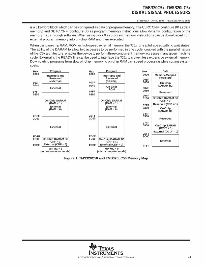
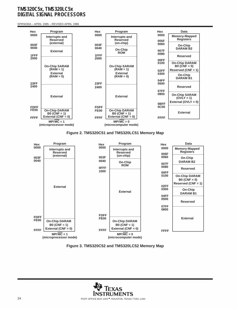
memory
The ’C5x implements three separate address spaces for program memory, data memory, and I/O. Each spaceaccommodates a total of 64K 16-bit words (see Figures 1 through 7). Within the 64K words of data space, the256 to 32K words at the top of the address range can be defined to be external global memory in incrementsof powers of two, as specified by the contents of the global memory allocation register (GREG). Access to globalmemory is arbitrated using the global memory bus request (BR) signal.
The ’C5x devices include a considerable amount of on-chip memory to aid in system performance andintegration including ROM, single-access RAM (SARAM), and dual-access RAM (DARAM). The amount andtypes of memory available on each device are shown in Table 1.
On the ’C5x, the first 96 (0–5Fh) data-memory locations are allocated for memory-mapped registers. Thismemory-mapped register space contains various control and status registers including those for the CPU, serialport, timer, and software wait-state generators. Additionally, the first 16 I/O port locations are mapped into thisdata-memory space, allowing them to be accessed either as data memory using single-word instructions or asI/O locations with two-word instructions. Two-word instructions allow access to the full 64K words of I/O space.
The mask-programmable ROM is located in program memory space. Customers can arrange to have this ROMprogrammed with contents unique to to any particular application. The ROM is enabled or disabled by the stateof the MP/MC control input upon resetting the device or by manipulating the MP/MC bit in the PMST statusregister after reset. The ROM occupies the lowest block of program memory when enabled. When disabled,these addresses are located in the device’s external program-memory space.
The ’C5x also has a mask-programmable option that provides security protection for the contents of on-chipROM. When this internal option bit is programmed, no externally-originating instruction can access the on-chipROM. This feature can be used to provide security for proprietary algorithms.
An optional boot loader is available in the device’s on-chip ROM. This boot loader can be used to transfer aprogram automatically from data memory or the serial port to anywhere in program memory. In data memory,the program can be located on any 1K-word boundary and can be in either byte-wide or 16-bit word format. Oncethe code is transferred, the boot loader releases control to the program for execution.
The ’C5x devices provide two types of RAM: single-access RAM (SARAM) and dual-access RAM (DARAM).The single-access RAM requires a full machine cycle to perform a read or a write; however, this is not one largeRAM block in which only one access per cycle is allowed. It is made up of 2K-word size-independent RAM blocksand each one allows one CPU access per cycle. The CPU can read or write one block while accessing anotherblock at the same time. All ’C5x processors support multiple accesses to its SARAM in one cycle as long as theygo to different RAM blocks. If the total SARAM size is not a multiple of two, one block is made smaller than 2Kwords. With an understanding of this structure, programmers can arrange code and data appropriately toimprove code performance. Table 4 shows the sizes of available SARAM on the applicable ’C5x devices.
Table 4. SARAM Block Sizes
DEVICE NUMBER OF SARAM BLOCKS
’C50/ ’LC50 Four 2K blocks and one 1K block
’C51/ ’LC51 One 1K block
’C53/ ’C53S / ’LC53 One 2K block and one 1K block
’LC56 Three 2K blocks
’C57S/ ’LC57/’LC57S Three 2K blocks
memory (continued)
The ’C5x dual-access RAM (DARAM) allows writes to, and reads from, the RAM in the same cycle without theaddress restrictions of the SARAM. The dual-access RAM is configured in three blocks: block 0 (B0), block 1(B1), and block 2 (B2). Block 1 is 512 words in data memory and block 2 is 32 words in data memory. Block 0
TMS320C5x, TMS320LC5xDIGITAL SIGNAL PROCESSORS
SPRS030A – APRIL 1995 – REVISED APRIL 1996
23POST OFFICE BOX 1443 • HOUSTON, TEXAS 77251–1443
is a 512-word block which can be configured as data or program memory. The CLRC CNF (configure B0 as datamemory) and SETC CNF (configure B0 as program memory) instructions allow dynamic configuration of thememory maps through software. When using block 0 as program memory, instructions can be downloaded fromexternal program memory into on-chip RAM and then executed.
When using on-chip RAM, ROM, or high-speed external memory, the ’C5x runs at full speed with no wait states.The ability of the DARAM to allow two accesses to be performed in one cycle, coupled with the parallel natureof the ’C5x architecture, enables the device to perform three concurrent memory accesses in any given machinecycle. Externally, the READY line can be used to interface the ’C5x to slower, less expensive external memory.Downloading programs from slow off-chip memory to on-chip RAM can speed processing while cutting systemcosts.
ProgramHex
Interrupts andReserved(external)
Data
External
Interrupts andReserved(on-chip)
On-ChipROM
External
Program
On-Chip SARAM(RAM = 1)External
(RAM = 0)
External
MP/MC = 0(microcomputer mode)
MP/MC = 1(microprocessor mode)
On-Chip DARAM B0(CNF = 1)
External (CNF = 0)
0000
003F0040
07FF0800
2BFF2C00
FDFFFE00
FFFF
0000
003F0040
07FF0800
2BFF2C00
FDFFFE00
FFFF
0000
005F0060
007F0080
0100
02FF
2C00
FFFF
00FF
0300
04FF0500
07FF0800
2BFF
Memory-MappedRegisters
On-ChipDARAM B2
Reserved
On-ChipDARAM B1
Reserved
On-Chip SARAM(OVLY = 1)
External (OVLY = 0)
External
On-Chip DARAM B0(CNF = 0)
Reserved (CNF = 1)
Hex Hex
On-Chip SARAM(RAM = 1)External
(RAM = 0)
On-Chip DARAM B0(CNF = 1)
External (CNF = 0)
Figure 1. TMS320C50 and TMS320LC50 Memory Map
TMS320C5x, TMS320LC5xDIGITAL SIGNAL PROCESSORS
SPRS030A – APRIL 1995 – REVISED APRIL 1996
24 POST OFFICE BOX 1443 • HOUSTON, TEXAS 77251–1443
Interrupts andReserved(on-chip)
Interrupts andReserved(external)
Memory-MappedRegisters
On-ChipDARAM B2
Reserved
On-ChipDARAM B1
Reserved
On-Chip SARAM(OVLY = 1)
External (OVLY = 0)
External
Data
External
Program
On-ChipROM
External
Program
External
MP/MC = 0(microcomputer mode)
MP/MC = 1(microprocessor mode)
On-Chip DARAMB0 (CNF = 0)
Reserved (CNF = 1)
On-Chip DARAMB0 (CNF = 1)
External (CNF = 0)
0000
003F0040
1FFF2000
23FF2400
FDFFFE00
FFFF
0000
003F0040
1FFF2000
23FF2400
FDFFFE00
FFFF
0000
005F0060
007F0080
0100
02FF
0C00
FFFF
00FF
0300
04FF0500
07FF0800
0BFF
Hex Hex Hex
On-Chip SARAM(RAM = 1)External
(RAM = 0)
On-Chip SARAM(RAM = 1)External
(RAM = 0)
On-Chip DARAMB0 (CNF = 1)
External (CNF = 0)
Figure 2. TMS320C51 and TMS320LC51 Memory Map
ProgramHex
Interrupts andReserved(external)
Data
Interrupts andReserved(on-chip)
On-ChipROM
External
Program
External
MP/MC = 0(microcomputer mode)
MP/MC = 1(microprocessor mode)
On-Chip DARAMB0 (CNF = 1)
External (CNF = 0)
0000
003F0040
FDFFFE00
FFFF
0000
003F0040
0FFF1000
FDFFFE00
FFFF
0000
005F0060
007F0080
0100
02FF
FFFF
00FF
0300
04FF0500
07FF0800
Memory-MappedRegisters
On-ChipDARAM B2
Reserved
On-ChipDARAM B1
Reserved
External
On-Chip DARAMB0 (CNF = 0)
Reserved (CNF = 1)
Hex Hex
On-Chip DARAMB0 (CNF = 1)
External (CNF = 0)
Figure 3. TMS320C52 and TMS320LC52 Memory Map
TMS320C5x, TMS320LC5xDIGITAL SIGNAL PROCESSORS
SPRS030A – APRIL 1995 – REVISED APRIL 1996
25POST OFFICE BOX 1443 • HOUSTON, TEXAS 77251–1443
Interrupts andReserved(external)
Memory-MappedRegisters
On-ChipDARAM B2
Reserved
On-ChipDARAM B1
Reserved
External
Data
External
Program
Interrupts andReserved(on-chip)
On-ChipROM
External
Program
On-Chip SARAM(RAM = 1)External
(RAM = 0)
External
MP/MC = 0(microcomputer mode)
MP/MC = 1(microprocessor mode)
On-Chip DARAMB0 (CNF = 0)
Reserved (CNF = 1)
On-Chip DARAMB0 (CNF = 1)
External (CNF = 0)
On-Chip DARAMB0 (CNF = 1)
External (CNF = 0)
0000
003F0040
3FFF4000
4BFF4C00
FDFFFE00
FFFF
0000
005F0060
007F0080
0100
02FF
1400
FFFF
0000
003F0040
3FFF4000
FDFFFE00
FFFF
00FF
0300
04FF0500
07FF0800 On-Chip SARAM
(OVLY = 1)External (OVLY = 0)
13FF
Hex Hex Hex
4BFF4C00
On-Chip SARAM(RAM = 1)External
(RAM = 0)
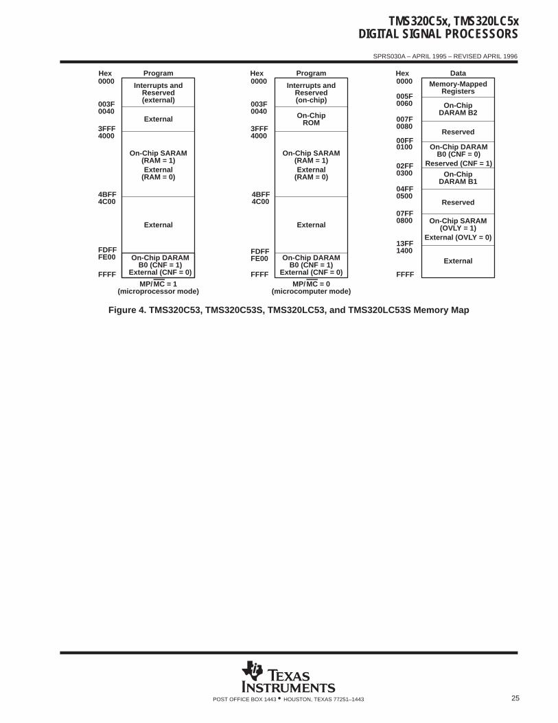
Figure 4. TMS320C53, TMS320C53S, TMS320LC53, and TMS320LC53S Memory Map
TMS320C5x, TMS320LC5xDIGITAL SIGNAL PROCESSORS
SPRS030A – APRIL 1995 – REVISED APRIL 1996
26 POST OFFICE BOX 1443 • HOUSTON, TEXAS 77251–1443
Data
1800
FFFF
20001FFF
17FF
10000FFF
080007FF
050004FF
030002FF
010000FF
0080007F0060005F
0000
Reserved
Reserved (CNF = 1)
On-Chip DARAM B1
(OVLY = 1)
External (OVLY = 0)
External (OVLY = 0)
(OVLY = 1)
External
External (OVLY = 0)
On-Chip DARAM B0 (CNF = 0)
On-Chip SARAM Blk0BSP Block (OVLY = 1)
On-Chip SARAM Blk1
On-Chip SARAM Blk2
Reserved
On-Chip DARAM B2
RegistersMemory-Mapped
Hex
On-Chip ROM
0000
7FFF8000
(RAM = 1)
(RAM = 1)
87FF8800
External (RAM = 0)
External (RAM = 0)
(RAM = 1)
9000
97FF9800
External (RAM = 0)
8FFF
External
(CNF = 1)
MP/MC = 0
FDFFFE00
FFFF
On-Chip DARAM B0
External (CNF = 0)
On-Chip SARAM Blk1
On-Chip SARAM Blk2
On-Chip SARAM Blk0
MP/MC = 1
External (CNF = 0)(CNF = 1)
On-Chip DARAM B0
External
External (RAM = 0)(RAM = 1)
On-Chip SARAM Blk2
External (RAM = 0)(RAM = 1)
On-Chip SARAM Blk1
External (RAM = 0)(RAM = 1)
On-Chip SARAM Blk0
External
FFFF
FE00FDFF
980097FF
90008FFF
880087FF
80007FFF
0000Program ProgramHex Hex
Interrupts and Reserved(on-chip)
Interrupts and Reservrd(external)
0040003F
0040003F
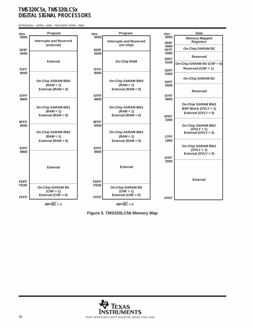
Figure 5. TMS320LC56 Memory Map
TMS320C5x, TMS320LC5xDIGITAL SIGNAL PROCESSORS
SPRS030A – APRIL 1995 – REVISED APRIL 1996
27POST OFFICE BOX 1443 • HOUSTON, TEXAS 77251–1443
On-Chip ROM
0000
7FFF8000
(RAM = 1)
(RAM = 1)
87FF8800
External (RAM = 0)
External (RAM = 0)
(RAM = 1)
9000
97FF9800
External (RAM = 0)
8FFF
External
(CNF = 1)
MP/MC = 0
FDFFFE00
FFFF
On-Chip DARAM B0
External (CNF = 0)
On-Chip SARAM Blk1
On-Chip SARAM Blk2
On-Chip SARAM Blk0
MP/MC = 1
External (CNF = 0)(CNF = 1)
On-Chip DARAM B0
External
External (RAM = 0)(RAM = 1)
On-Chip SARAM Blk2
External (RAM = 0)(RAM = 1)
On-Chip SARAM Blk1
External (RAM = 0)(RAM = 1)
On-Chip SARAM Blk0
External
FFFF
FE00FDFF
980097FF
90008FFF
880087FF
80007FFF
0000Program ProgramHex Hex Data
Memory-MappedRegisters
Reserved
0000
0060
0080
005F
007F
0100
0300
00FF
02FF
On-Chip DARAM B2
Reserved (CNF = 1)On-Chip DARAM (CNF = 0)
Reserved
0500
0800
04FF
07FF
10000FFF
External (OVLY = 0)
HPI Block (OVLY = 1)
(OVLY = 1)
180017FF
20001FFF
External (OVLY = 0)
External (OVLY = 0)
External
FFFF
On-Chip SARAM Blk2
On-Chip SARAM Blk1
On-Chip SARAM Blk0BSP Block (OVLY = 1)
On-Chip DARAM B1
Hex
HPI Control Register0501
Interrupts and Reserved(on-chip)
Interrupts and Reservrd(external)
0040003F
0040003F
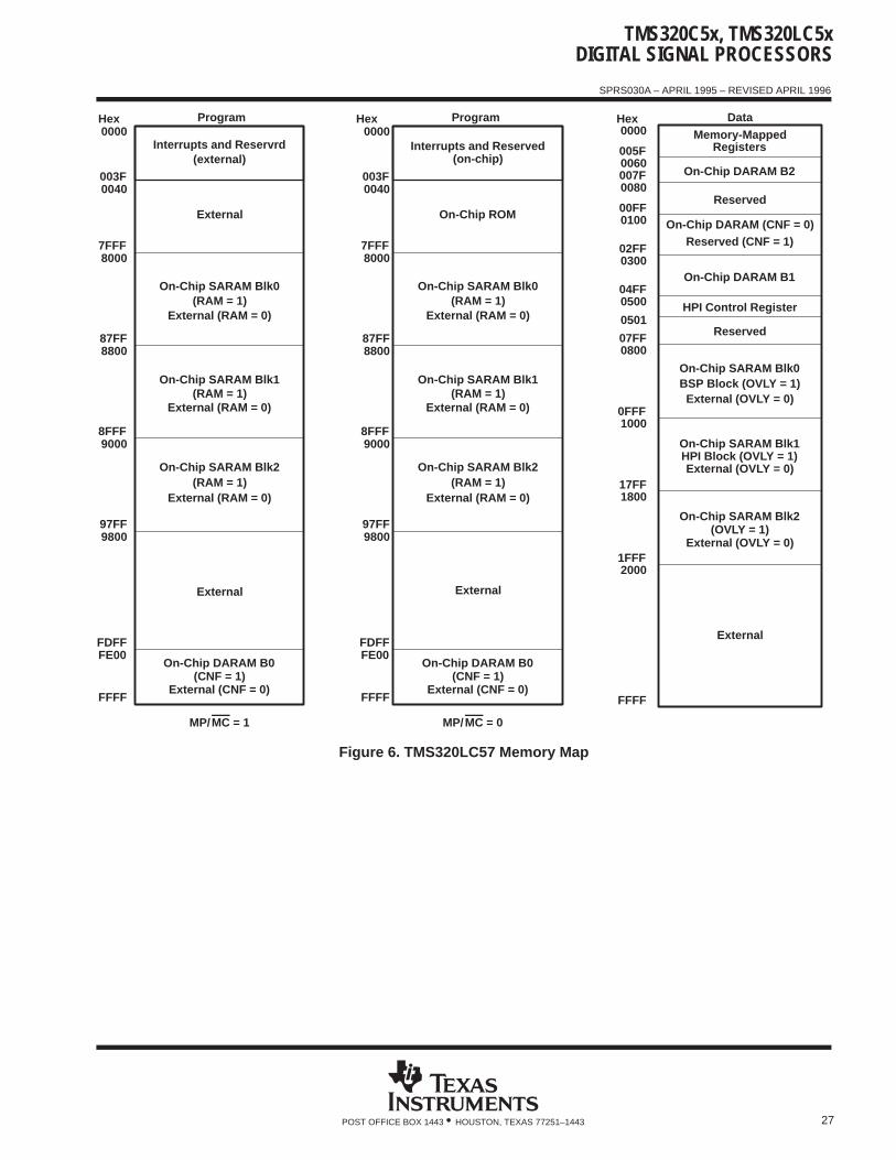
Figure 6. TMS320LC57 Memory Map

TMS320C5x, TMS320LC5xDIGITAL SIGNAL PROCESSORS
SPRS030A – APRIL 1995 – REVISED APRIL 1996
28 POST OFFICE BOX 1443 • HOUSTON, TEXAS 77251–1443
On-Chip ROM
0000
7FFF8000
(RAM = 1)
(RAM = 1)
87FF8800
External (RAM = 0)
External (RAM = 0)
(RAM = 1)
9000
97FF9800
External (RAM = 0)
8FFF
External
(CNF = 1)
MP/MC = 0
FDFFFE00
FFFF
On-Chip DARAM B0
External (CNF = 0)
On-Chip SARAM Blk1
On-Chip SARAM Blk2
On-Chip SARAM Blk0
MP/MC = 1
External (CNF = 0)(CNF = 1)
On-Chip DARAM B0
External
External (RAM = 0)(RAM = 1)
On-Chip SARAM Blk2
External (RAM = 0)(RAM = 1)
On-Chip SARAM Blk1
External (RAM = 0)(RAM = 1)
On-Chip SARAM Blk0
External
FFFF
FE00FDFF
980097FF
90008FFF
880087FF
80007FFF
0000Program ProgramHex Hex Data
Memory-MappedRegisters
Reserved
0000
0060
0080
005F
007F
0100
0300
00FF
02FF
On-Chip DARAM B2
Reserved (CNF = 1)On-Chip DARAM (CNF = 0)
HPI Control Register0500
0800
04FF
07FF
10000FFF
External (OVLY = 0)
HPI Block (OVLY = 1)
(OVLY = 1)
180017FF
20001FFF
External (OVLY = 0)
External (OVLY = 0)
External
FFFF
On-Chip SARAM Blk2
On-Chip SARAM Blk1
On-Chip SARAM Blk0BSP Block (OVLY = 1)
On-Chip DARAM B1
Hex
External
07FF0800
Reserved0501
Interrupts and Reserved(on-chip)
Interrupts and Reservrd(external)
0040003F
0040003F
Figure 7. TMS320C57S Memory Map
TMS320C5x, TMS320LC5xDIGITAL SIGNAL PROCESSORS
SPRS030A – APRIL 1995 – REVISED APRIL 1996
29POST OFFICE BOX 1443 • HOUSTON, TEXAS 77251–1443
interrupts and subroutines
The ’C5x implements four general-purpose interrupts, INT4–INT1, along with reset (RS) and the nonmaskableinterrupt (NMI) which are available for external devices to request the attention of the processor. Internalinterrupts are generated by the serial port (RINT and XINT), by the timer (TINT), and by the software-interrupt(TRAP, INTR, and NMI) instructions. Interrupts are prioritized with RS having the highest priority, followed byNMI, and INT4 having the lowest priority. Additionally, any interrupt except RS and NMI can be maskedindividually with a dedicated bit in the interrupt mask register (IMR) and can be cleared, set, or tested using itsown dedicated bit in the interrupt flag register (IFR). The reset and NMI functions are not maskable.
All interrupt vector locations are on two-word boundaries so that branch instructions can be accommodated inthose locations. While normally located at program memory address 0, the interrupt vectors can be remappedto the beginning of any 2K-word page in program memory by modifying the contents of the interrupt vectorpointer (IPTR) located in the PMST status register.
A built-in mechanism protects multicycle instructions from interrupts. If an interrupt occurs during a multicycleinstruction, the interrupt is not processed until the instruction completes execution. This mechanism applies toinstructions that are repeated (using the RPT instruction) and to instructions that become multicycle becauseof wait states.
Each time an interrupt is serviced or a subroutine is entered, the PC is pushed onto an internal hardware stack,providing a mechanism for returning to the previous context. The stack contains eight locations, allowinginterrupts or subroutines to be nested up to eight levels deep.
In addition to the eight-level hardware PC stack, eleven key CPU registers are equipped with an associatedsingle-level stack or shadow register into which the registers’ contents are saved upon servicing an interrupt.The contents are restored into their particular CPU registers once a return-from-interrupt instruction (RETE orRETI) is executed. The registers that have the shadow-register feature include the ACC and buffer, productregister, status registers, and several other key CPU registers. The shadow-register feature allowssophisticated context save and restore operations to be handled automatically in cases where nested interruptsare not required or if interrupt servicing is performed serially.
power-down modes
The ’C5x implements several power-down modes in which the ’C5x core enters a dormant state and dissipatesconsiderably less power. A power-down mode is invoked either by executing the IDLE/IDLE2 instructions orby driving the HOLD input low. When the HOLD signal initiates the power-down mode, on-chip peripheralscontinue to operate; this power-down mode is terminated when HOLD goes inactive.
While the ’C5x is in a power-down mode, all internal contents are maintained; this allows operation to continueunaltered when the power-down mode is terminated. All CPU activities are halted when the IDLE instructionis executed, but the CLKOUT1 pin remains active. The peripheral circuits continue to operate, allowingperipherals such as serial ports and timers to take the CPU out of its powered-down state. A power-down mode,when initiated by an IDLE instruction, is terminated upon receipt of an interrupt.
The IDLE2 instruction is used for a complete shutdown of the core CPU as well as all on-chip peripherals. InIDLE2, the power is reduced significantly because the entire device is stopped. The power-down mode isterminated by activating any of the external interrupt pins (RS, NMI, INT1, INT2, INT3, and INT4) for at leastfive machine cycles.
bus-keeper circuitry (TMS320LC56/’C57S/’LC57)
The TMS320LC56/’C57S/’LC57 devices provide built-in bus keeper circuitry which holds the last state drivenon the data bus by either the DSP or an external device after the bus is no longer being driven. This capabilityprevents excess power consumption caused by a floating bus, thus allowing optimization of power consumptionwithout the need for external pullup resistors.
TMS320C5x, TMS320LC5xDIGITAL SIGNAL PROCESSORS
SPRS030A – APRIL 1995 – REVISED APRIL 1996
30 POST OFFICE BOX 1443 • HOUSTON, TEXAS 77251–1443
external interface
The ’C5x supports a wide range of system interfacing requirements. Program, data, and I/O address spacesprovide interface to memory and I/O, maximizing system throughput. The full 16-bit address and data bus, alongwith the PS, DS, and IS space select signals, allow addressing of 64K 16-bit words in each of the three spaces.
I/O design is simplified by having I/O treated the same way as memory. I/O devices are mapped into the I/Oaddress space using the processor’s external address and data buses in the same manner as memory-mappeddevices.
The ’C5x external parallel interface provides various control signals to facilitate interfacing to the device. TheR/W output signal is provided to indicate whether the current cycle is a read or a write. The STRB output signalprovides a timing reference for all external cycles. For convenience, the device also provides the RD and theWE output signals, which indicate a read and a write cycle, respectively, along with timing information for thosecycles. The availability of these signals minimizes external gating necessary for interfacing external devices tothe ’C5x.
Interface to memory and I/O devices of varying speeds is accomplished by using the READY line. Whentransactions are made with slower devices, the ’C5x processor waits until the other device completes its functionand signals the processor via the READY line. Once a ready indication is provided back to the ’C5x from theexternal device, execution continues.
The bus request (BR) signal is used in conjunction with the other ’C5x interface signals to arbitrate externalglobal-memory accesses. Global memory is external data-memory space in which the BR signal is assertedat the beginning of the access. When an external global-memory device receives the the bus request, theexternal device responds by asserting the READY signal after the global memory access is arbitrated and theglobal access is completed.
external direct-memory access (DMA) capability
All ’C5x devices with single-access RAM offer a unique feature allowing another processor to read and writeto the ’C5x internal memory. To initiate a read or write operation to the ’C5x single-access RAM, the host ormaster processor requests a hold state on the DSP’s external bus. When acknowledged with HOLDA, the hostcan request access to the internal bus by pulling the BR signal low. Unlike the hold mode, which allows thecurrent operation to complete and allows CPU operation to continue (if status bit HM=0), a BR-requested DMAalways halts the operation currently being executed by the CPU. Access to the internal bus always is grantedon the third clock cycle after the BR signal is received. In the PQ package, the IAQ pin also indicates when busaccess has been granted. In the PZ package, this pin is not present so the host is required to wait two clockcycles after driving the bus request low before beginning DMA transfer.
host port interface (HPI) (TMS320C57S, TMS320LC57, TMS320LC57S only)
The HPI is an 8-bit parallel port used to interface a host processor to the ’C57S/’LC57. The host port isconnected to a 2k word on-chip buffer through a dedicated internal bus. The dedicated bus allows the CPU towork uninterrupted while the host processor accesses the host port. The HPI memory buffer is a single-accessRAM block which is accessible by both the CPU and the host. The HPI memory also can be used asgeneral-purpose data or program memory. Both the CPU and the host have access to the HPI control register(HPIC) and the host can address the HPI memory through the HPI address register (HPIA).
Data transfers of 16-bit words occur as two consecutive bytes with a dedicated pin, HBIL, indicating whetherthe high or low byte is being transmitted. Two control pins, HCNTL1 and HCNTL0, control host access to theHPIA, HPI data (with an optional automatic address increment), or the HPIC. The host can interrupt the’C57S/’LC57 by writing to HPIC. The ’C57S/’LC57 can interrupt the host with a dedicated HINT pin that the hostacknowledges and clears.
TMS320C5x, TMS320LC5xDIGITAL SIGNAL PROCESSORS
SPRS030A – APRIL 1995 – REVISED APRIL 1996
31POST OFFICE BOX 1443 • HOUSTON, TEXAS 77251–1443
host port interface (continued)
The HPI has two modes of operation, shared-access mode (SAM) and host-only mode (HOM). In SAM, thenormal mode of operation, both the ’C57S/’LC57 and the host can access HPI memory. In this mode,asynchronous host accesses are resynchronized internally and, in case of conflict, the host has access priorityand the ’C57S/’LC57S waits one cycle. Host and CPU accesses to the HPI memory can be resychronizedthrough polling of a command word or through interrupts to prevent stalling the CPU for one cycle. The HOMcapability allows the host to access HPI memory while the ’C57S/’LC57 is in IDLE2 mode (all internal clocksstopped) or in reset mode. The external ’C57S/’LC57S clock even can be stopped. The host can, therefore,access the HPI RAM while the ’C57S/’LC57 is in its optimum configuration in terms of power consumption.
The HPI control register has two data strobes, HDS1 and HDS2, a read/write strobe HR/W, and an addressstrobe HAS, to enable a glueless interface to a variety of industry-standard host devices. The HPI is easilyinterfaced to hosts with multiplexed address/data bus, separate address and data buses, one data strobe, anda read/write strobe, or two separate strobes for read and write. An HPI-ready pin, HRDY, is provided to specifywait states for hosts that support an asynchronous input. When the ’C57S/’LC57 operating frequency isvariable, or when the host is capable of accessing at a faster rate than the maximum shared-access modeaccess rate, the HRDY pin provides a convenient way to adjust the host access rate automatically (no softwarehandshake needed) to a change in the ’C57S/’LC57 clock rate or an HPI-mode switch.
The HPI supports high-speed back-to-back accesses. In the shared-access mode, the HPI can handle one byteevery five ’C57S/’LC57 periods (that is, 64 Mb/s with a 40-MHz ’C57S/’LC57). The HPI is designed so that thehost can take advantage of this high bandwidth and run at frequencies up to (f n) ÷ 5, where n is the numberof host cycles for an external access and f is the ’C57S/’LC57 frequency. In host-only mode, the HPI supportseven higher speed back-to-back host accesses: 1 byte every 50 ns (that is, 160 Mb/s) independently of the’C57S/’LC57 clock rate.
serial ports
The ’C5x provides high-speed full-duplex serial ports that allow direct interface to other ’C5x devices, codecs,and other devices in a system. There is a general-purpose serial port, a time-division-multiplexed (TDM) serialport, and an auto-buffered serial port (BSP).
The general-purpose serial port uses two memory-mapped registers for data transfer: the data-transmit register(DXR) and the data-receive register (DRR). Both registers can be accessed in the same manner as any othermemory location. The transmit and receive sections of the serial port each have associated clocks,frame-synchronization pulses, and serial shift registers, and serial data can be transferred either in bytes or in16-bit words. Serial port receive and transmit operations can generate their own maskable transmit and receiveinterrupts (XINT and RINT), allowing serial port transfers to be managed by way of software. The ’C5x serialports are double-buffered and fully static.
The TDM port allows the device to communicate through time-division multiplexing with up to seven other ’C5xdevices with TDM ports. Time-division multiplexing is the division of time intervals into a number of subintervalswith each subinterval representing a prespecified communications channel. The TDM port serially transmits16-bit words on a single data line (TDAT) and destination addresses on a single address line (TADD). Eachdevice can transmit data on a single channel and receive data from one or more of the eight channels providinga simple and efficient interface for multiprocessing applications. A frame synchronization pulse occurs onceevery 128 clock cycles corresponding to transmission of one 16-bit word on each of the eight channels. Likethe general-purpose serial port, the TDM port is double-buffered on both input and output data. The TDM portalso can be configured in software to operate as a general-purpose serial port as described above. Both typesof ports are capable of operating at up to one-fourth the machine cycle rate (CLKOUT1).
The buffered serial port (BSP) consists of a full-duplex double-buffered serial port interface (SPI) and anauto-buffering unit (ABU). The SPI block of the BSP is an enhanced version of the general-purpose serial port.The auto-buffering unit allows the SPI to read/write directly to ’C5x internal memory using a dedicated busindependently of the CPU. This results in minimum overhead for SPI transactions and faster data rates.
TMS320C5x, TMS320LC5xDIGITAL SIGNAL PROCESSORS
SPRS030A – APRIL 1995 – REVISED APRIL 1996
32 POST OFFICE BOX 1443 • HOUSTON, TEXAS 77251–1443
serial ports (continued)
When auto-buffering capability is disabled (standard mode), transfers with SPI are performed under softwarecontrol through interrupts. In this mode, the ABU is transparent and the word-based interrupts (WXINT andWRINT) provided by the SPI are sent to the CPU as transmit interrupt (XINT) and receive interrupt (RINT).When auto buffering is enabled, word transfers are done directly between the SPI and the ’C5x internal memory,using ABU-embedded address generators.
The ABU has its own set of circular addressing registers with corresponding address-generation units. Memoryfor the buffers resides in 2K words of ’C5x internal memory. The length and starting addresses of the buffersare user-programmable. A buffer-empty/- full interrupt can be posted to the CPU. Buffering is halted easilybecause of an auto-disabling capability. Auto-buffering capability can be enabled separately for transmit andreceive sections. When auto-buffering is disabled, operation is similar to the general-purpose serial port.
The SPI allows transfer of 8-, 10-, 12-, or 16-bit data packets. In burst mode, data packets are directed by aframe-synchronization pulse for every packet. In continuous mode, the frame-synchronization pulse occurswhen the data transmission is initiated and no further pulses occur. The frame and clock strobes are frequencyand polarity programmable. The SPI is fully static and operates at arbitrarily low clock frequencies. Themaximum operating frequency is CLKOUT1 (28.6 Mb/s at 35 ns, 40 Mb/s at 25 ns). The SPI transmit sectionalso includes a pulse-coded modulation (PCM) mode that allows easy interface with a PCM line.
Most ’C5x devices provide one general-purpose serial port and one TDM port. The ’C52 provides onegeneral-purpose serial port and no TDM port. The ’C53SX provides two general-purpose serial ports and noTDM port. The ’LC56, ’C57S, and ’LC57 devices provide one general-purpose serial port and one buffered serialport.
software wait-state generators
Software wait-state generation is incorporated in the ’C5x without any external hardware for interfacing withslower off-chip memory and I/O devices. The circuitry consists of 16 wait-state generating circuits and isuser-programmable to operate with 0, 1, 2, 3, or 7 wait states. For off-chip memory accesses, these wait-stategenerators are mapped on 16K-word boundaries in program memory, data memory, and the I/O ports.
The ’C53S/’C57S and ’LC56/57 devices have software-programmable wait-state generators that are controlledby one 16-bit wait-state register PDWSR at address 0x28. The programmed number of wait states (0 through7) applies to all external addresses at the corresponding address space (program, data, I/O) regardless ofaddress value.
timer
The ’C5x features a 16-bit timing circuit with a 4-bit prescaler. This timer clocks between one-half and onethirty-second the machine rate of the device itself, depending on the programmable timer’s divide-down ratio.This timer can be stopped, restarted, reset, or disabled by specific status bits.
The timer can be used to generate CPU interrupts periodically. The timer is decremented by one at everyCLKOUT1 cycle. A timer interrupt (TINT) and a pulse equal to the duration of a CLKOUT1 cycle on the externalTOUT pin are generated each time the counter decrements to zero. The timer provides a convenient meansof performing periodic I/O or other functions. When the timer is stopped, the internal clocks to the timer are shutoff, allowing the device to run in a low-power mode of operation.
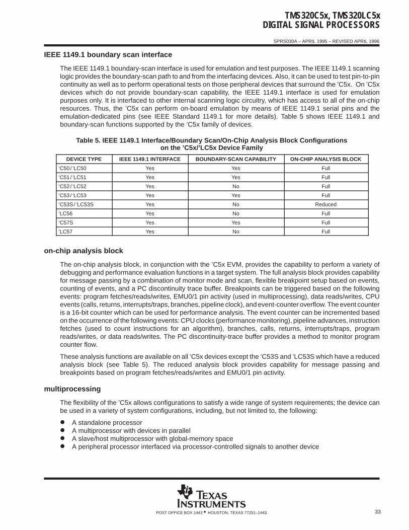
TMS320C5x, TMS320LC5xDIGITAL SIGNAL PROCESSORS
SPRS030A – APRIL 1995 – REVISED APRIL 1996
33POST OFFICE BOX 1443 • HOUSTON, TEXAS 77251–1443
IEEE 1149.1 boundary scan interface
The IEEE 1149.1 boundary-scan interface is used for emulation and test purposes. The IEEE 1149.1 scanninglogic provides the boundary-scan path to and from the interfacing devices. Also, it can be used to test pin-to-pincontinuity as well as to perform operational tests on those peripheral devices that surround the ’C5x. On ’C5xdevices which do not provide boundary-scan capability, the IEEE 1149.1 interface is used for emulationpurposes only. It is interfaced to other internal scanning logic circuitry, which has access to all of the on-chipresources. Thus, the ’C5x can perform on-board emulation by means of IEEE 1149.1 serial pins and theemulation-dedicated pins (see IEEE Standard 1149.1 for more details). Table 5 shows IEEE 1149.1 andboundary-scan functions supported by the ’C5x family of devices.
Table 5. IEEE 1149.1 Interface/Boundary Scan/On-Chip Analysis Block Configurationson the ’C5x/’LC5x Device Family
DEVICE TYPE IEEE 1149.1 INTERFACE BOUNDARY-SCAN CAPABILITY ON-CHIP ANALYSIS BLOCK
’C50/ ’LC50 Yes Yes Full
’C51/ ’LC51 Yes Yes Full
’C52/ ’LC52 Yes No Full
’C53/ ’LC53 Yes Yes Full
’C53S/ ’LC53S Yes No Reduced
’LC56 Yes No Full
’C57S Yes Yes Full
’LC57 Yes No Full
on-chip analysis block
The on-chip analysis block, in conjunction with the ’C5x EVM, provides the capability to perform a variety ofdebugging and performance evaluation functions in a target system. The full analysis block provides capabilityfor message passing by a combination of monitor mode and scan, flexible breakpoint setup based on events,counting of events, and a PC discontinuity trace buffer. Breakpoints can be triggered based on the followingevents: program fetches/reads/writes, EMU0/1 pin activity (used in multiprocessing), data reads/writes, CPUevents (calls, returns, interrupts/traps, branches, pipeline clock), and event-counter overflow. The event counteris a 16-bit counter which can be used for performance analysis. The event counter can be incremented basedon the occurrence of the following events: CPU clocks (performance monitoring), pipeline advances, instructionfetches (used to count instructions for an algorithm), branches, calls, returns, interrupts/traps, programreads/writes, or data reads/writes. The PC discontinuity-trace buffer provides a method to monitor programcounter flow.
These analysis functions are available on all ’C5x devices except the ’C53S and ’LC53S which have a reducedanalysis block (see Table 5). The reduced analysis block provides capability for message passing andbreakpoints based on program fetches/reads/writes and EMU0/1 pin activity.
multiprocessing
The flexibility of the ’C5x allows configurations to satisfy a wide range of system requirements; the device canbe used in a variety of system configurations, including, but not limited to, the following:
A standalone processor A multiprocessor with devices in parallel A slave/host multiprocessor with global-memory space A peripheral processor interfaced via processor-controlled signals to another device
TMS320C5x, TMS320LC5xDIGITAL SIGNAL PROCESSORS
SPRS030A – APRIL 1995 – REVISED APRIL 1996
34 POST OFFICE BOX 1443 • HOUSTON, TEXAS 77251–1443
multiprocessing (continued)
For multiprocessing applications, the ’C5x is capable of allocating global-memory space and communicatingwith that space via the BR and ready control signals. Global memory is data memory shared by more than onedevice. Global memory access must be arbitrated. The 8-bit memory-mapped global memory allocation register(GREG) specifies part of the ’C5x’s data memory as global external memory. The contents of the registerdetermine the size of the global memory space. If the current instruction addresses an operand within thatspace, BR is asserted to request control of the bus. The length of the memory cycle is controlled by the READYline.
The ’C5x supports direct memory access (DMA) to its external program, data, and I/O spaces using the HOLDand HOLDA signals. Another device can take complete control of the ’C5x’s external memory interface byasserting HOLD low. This causes the ’C5x to to place its address, data, and control lines in the high-impedancestate and assert HOLDA. While external memory is being accessed, program execution from on-chip memorycan proceed concurrently when the device is in hold mode.
Multiple ’C5x devices can be interconnected through their serial ports. This form of interconnection allowsinformation to be transferred at high speed while using a minimum number of signal connections. A completefull-duplex serial-port interconnection between multiple processors can be accomplished with as few as foursignal lines.
instruction set
The ’C5x microprocessor implements a comprehensive instruction set that supports both numeric-intensivesignal processing operations and general-purpose applications, such as multiprocessing and high-speedcontrol. Source code for the ’C1x and ’C2x DSPs is upward compatible with the ’C5x.
For maximum throughput, the next instruction is prefetched while the current one is being executed. Becausethe same data lines are used to communicate to external data, program, or I/O space, the number of cycles aninstruction requires to execute varies, depending on whether the next data operand fetch is from internal orexternal memory. Highest throughput is achieved by maintaining data memory on chip and using either internalor fast external program memory.
addressing modes
The ’C5x instruction set provides six basic memory-addressing modes: direct, indirect, immediate, register,memory mapped, and circular addressing.
In direct addressing, the instruction word contains the lowest seven bits of the data-memory address. This fieldis concatenated with the nine bits of the data-memory page pointer (DP) to form the 16-bit data-memoryaddress. Therefore, in the direct-addressing mode, data memory is paged effectively with a total of 512 pages,each of which contains 128 words.
Indirect addressing accesses data memory through the auxiliary registers. In indirect addressing mode, theaddress of the instruction operand is contained in the currently selected auxiliary register. Eight auxiliaryregisters (AR0–AR7) provide flexible and powerful indirect addressing. To select a specific auxiliary register,the auxiliary register pointer (ARP) is loaded with a value from 0 to 7 for AR0 through AR7, respectively.
There are seven types of indirect addressing: autoincrement or autodecrement, postindexing by either addingor subtracting the contents of AR0, single-indirect addressing with no increment or decrement, and bit-reversedaddressing (used in FFTs) with increment or decrement. All operations are performed on the current auxiliaryregister in the same cycle as the original instruction, following which the current auxiliary register and ARP canbe modified.
TMS320C5x, TMS320LC5xDIGITAL SIGNAL PROCESSORS
SPRS030A – APRIL 1995 – REVISED APRIL 1996
35POST OFFICE BOX 1443 • HOUSTON, TEXAS 77251–1443
addressing modes (continued)
In immediate addressing, the actual operand data is provided in a portion of the instruction word or words. Thereare two types of immediate addressing: long and short. In short-immediate addressing, the data is containedin a portion of the bits in a single-word instruction. In long-immediate addressing, the data is contained in thesecond word of a two-word instruction. The immediate-addressing mode is useful for data that does not needto be stored or used more than once during the course of program execution, such as initialization values,constants, etc.
The register-addressing mode uses operands in CPU registers either explicitly, such as with a direct referenceto a specific register, or implicitly, with instructions that intrinsically reference certain registers. In either case,operand reference is simplified because 16-bit values can be used without specifying a full 16-bit operandaddress or immediate value.
Memory-mapped addressing provides the convenience of easy access to memory-mapped registers locatedon page zero of data memory. The flexibility of memory-mapped addressing results because accesses aremade independently of actual DP value and without having to provide a complete address of the memorylocation being accessed. Commonly used on-board registers can be accessed with a simplified addressingscheme.
Circular addressing is the most sophisticated ’C5x addressing mode. This addressing mode allows specifiedbuffers in memory to be accessed sequentially with a pointer that automatically wraps around to the beginningof the buffer when the last location is accessed. A total of two independent circular buffers can be allocated atany given time.
Five dedicated registers are allocated for implementation of circular addressing: a beginning-of-buffer and anend-of-buffer register for each of the two independent circular buffers and a control register. Additionally, oneof the auxiliary registers is used as the pointer into the circular buffer. All registers used in circular addressingmust be initialized properly prior to performing any circular buffer access.
The circular-addressing mode allows implementation of circular buffers, which facilitate data structures usedin FIR filters, convolution and correlation algorithms, and waveform generators. Having the capability to accesscircular buffers automatically with no overhead allows these types of data structures to be implemented mostefficiently.
repeat feature
The repeat function can be used with instructions such as multiply/accumulates (MAC and MACD), block moves(BLDD and BLPD), I/O transfers (IN/OUT), and table read/writes (TBLR/TBLW). These instructions, althoughnormally multicycle, are pipelined when the repeat feature is used, and they effectively become single-cycleinstructions. For example, the table-read instruction may take three or more cycles to execute, but when theinstruction is repeated, a table location can be read every cycle.
The repeat counter (RPTC) is a 16-bit register that, when loaded with a number N, causes the next singleinstruction to be executed N + 1 times. The RPTC register is loaded by either the RPT or the RPTZ instruction,resulting in a maximum of 65,536 executions of a given instruction. RPTC is cleared by reset. The RPTZinstruction clears both ACC and PREG before the next instruction starts repeating. Once a repeat instruction(RPT or RPTZ) is decoded, all interrupts including NMI (except reset) are masked until the completion of therepeat loop. However, the device responds to the HOLD signal while executing an RPT/RPTZ loop.
repeat feature (continued)
The ’C5x implements a block-repeat feature that provides zero-overhead looping for implementation of FORand DO loops. The function is controlled by three registers (PASR, PAER, and BRCR) and the BRAF bit in thePMST register. The block-repeat counter register (BRCR) is loaded with a loop count of 0 to 65,535. Then,execution of the RPTB (repeat block) instruction loads the program-address-start register (PASR) with theaddress of the instruction following the RPTB instruction and loads the program-address-end register (PAER)
TMS320C5x, TMS320LC5xDIGITAL SIGNAL PROCESSORS
SPRS030A – APRIL 1995 – REVISED APRIL 1996
36 POST OFFICE BOX 1443 • HOUSTON, TEXAS 77251–1443
with its long-immediate operand. The long-immediate operand is the address of the instruction following the lastinstruction in the loop minus one. (The repeat block must contain at least three instruction words.) Executionof the RPTB instruction automatically sets active the BRAF bit. With each PC update, the PAER contents arecompared to the PC. If they are equal, the BRCR contents are compared to zero. If the BRCR contents aregreater than zero, BRCR is decremented and the PASR is loaded into the PC, repeating the loop. If not, theBRAF bit is set low and the processor resumes execution past the end of the code’s loop.
The equivalent of a WHILE loop can be implemented by setting the BRAF bit to zero if the exit condition is met.The program then completes the current pass through the loop but does not go back to the top. To exit, the bitmust be reset at least four instruction words before the end of the loop. It is possible to exit block-repeat loopsand return to them without stopping and restarting the loop. Branches, calls, and interrupts do not necessarilyaffect the loop. When program control is returned to the loop, loop execution is resumed.
instruction set summary
This section summarizes the operational codes (opcodes) of the instruction set for the ’C5x digital signalprocessors. The instruction set is a super set of the ’C1x and ’C2x instruction sets. The instructions are arrangedaccording to function and are alphabetized by mnemonic within each category. The symbols in Table 6 are usedin the instruction set opcode table (Table 7). The Texas Instruments ’C5x assembler accepts ’C2x instructionsas well as ’C5x instructions.
The number of words that an instruction occupies in program memory is specified in column 4 of Table 7. Inthese cases, different forms of the instruction occupy a different number of words. For example, the ADDinstruction occupies one word when the operand is a short immediate value or two words if the operand is along immediate value.
The number of cycles that an instruction requires to execute is listed in column 5 of Table 7. All instructions areassumed to be executed from internal program memory and internal data dual-access memory. The cycletimings are for single-instruction execution, not for repeat mode.
A read or write access to any peripheral memory-mapped register in data memory locations 20h–4Fh adds onecycle to the cycle time shown because all peripherals perform these accesses over the internal peripheral bus.
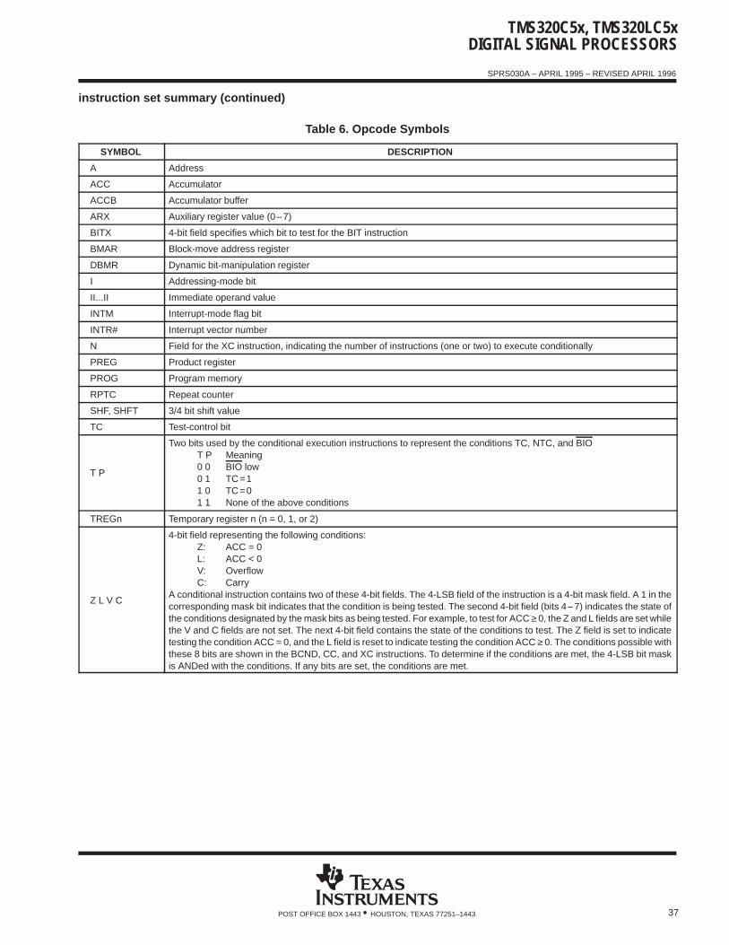
TMS320C5x, TMS320LC5xDIGITAL SIGNAL PROCESSORS
SPRS030A – APRIL 1995 – REVISED APRIL 1996
37POST OFFICE BOX 1443 • HOUSTON, TEXAS 77251–1443
instruction set summary (continued)
Table 6. Opcode Symbols
SYMBOL DESCRIPTION
A Address
ACC Accumulator
ACCB Accumulator buffer
ARX Auxiliary register value (0–7)
BITX 4-bit field specifies which bit to test for the BIT instruction
BMAR Block-move address register
DBMR Dynamic bit-manipulation register
I Addressing-mode bit
II...II Immediate operand value
INTM Interrupt-mode flag bit
INTR# Interrupt vector number
N Field for the XC instruction, indicating the number of instructions (one or two) to execute conditionally
PREG Product register
PROG Program memory
RPTC Repeat counter
SHF, SHFT 3/4 bit shift value
TC Test-control bit
T P
Two bits used by the conditional execution instructions to represent the conditions TC, NTC, and BIOT P Meaning0 0 BIO low0 1 TC=11 0 TC=01 1 None of the above conditions
TREGn Temporary register n (n = 0, 1, or 2)
Z L V C
4-bit field representing the following conditions:Z: ACC = 0L: ACC < 0V: OverflowC: Carry
A conditional instruction contains two of these 4-bit fields. The 4-LSB field of the instruction is a 4-bit mask field. A 1 in thecorresponding mask bit indicates that the condition is being tested. The second 4-bit field (bits 4–7) indicates the state ofthe conditions designated by the mask bits as being tested. For example, to test for ACC ≥ 0, the Z and L fields are set whilethe V and C fields are not set. The next 4-bit field contains the state of the conditions to test. The Z field is set to indicatetesting the condition ACC = 0, and the L field is reset to indicate testing the condition ACC ≥ 0. The conditions possible withthese 8 bits are shown in the BCND, CC, and XC instructions. To determine if the conditions are met, the 4-LSB bit maskis ANDed with the conditions. If any bits are set, the conditions are met.
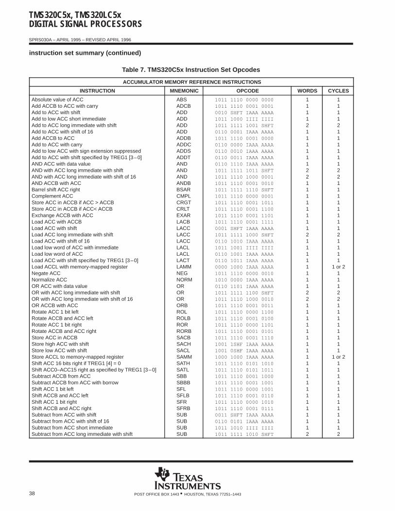
TMS320C5x, TMS320LC5xDIGITAL SIGNAL PROCESSORS
SPRS030A – APRIL 1995 – REVISED APRIL 1996
38 POST OFFICE BOX 1443 • HOUSTON, TEXAS 77251–1443
instruction set summary (continued)
Table 7. TMS320C5x Instruction Set Opcodes
ACCUMULATOR MEMORY REFERENCE INSTRUCTIONS
INSTRUCTION MNEMONIC OPCODE WORDS CYCLES
Absolute value of ACCAdd ACCB to ACC with carryAdd to ACC with shiftAdd to low ACC short immediateAdd to ACC long immediate with shiftAdd to ACC with shift of 16Add ACCB to ACCAdd to ACC with carryAdd to low ACC with sign extension suppressedAdd to ACC with shift specified by TREG1 [3–0]AND ACC with data valueAND with ACC long immediate with shiftAND with ACC long immediate with shift of 16AND ACCB with ACCBarrel shift ACC rightComplement ACCStore ACC in ACCB if ACC > ACCBStore ACC in ACCB if ACC< ACCBExchange ACCB with ACCLoad ACC with ACCBLoad ACC with shiftLoad ACC long immediate with shiftLoad ACC with shift of 16Load low word of ACC with immediateLoad low word of ACCLoad ACC with shift specified by TREG1 [3–0]Load ACCL with memory-mapped registerNegate ACCNormalize ACCOR ACC with data valueOR with ACC long immediate with shiftOR with ACC long immediate with shift of 16OR ACCB with ACCRotate ACC 1 bit leftRotate ACCB and ACC leftRotate ACC 1 bit rightRotate ACCB and ACC rightStore ACC in ACCBStore high ACC with shiftStore low ACC with shiftStore ACCL to memory-mapped registerShift ACC 16 bits right if TREG1 [4] = 0Shift ACC0–ACC15 right as specified by TREG1 [3–0]Subtract ACCB from ACCSubtract ACCB from ACC with borrowShift ACC 1 bit leftShift ACCB and ACC leftShift ACC 1 bit rightShift ACCB and ACC rightSubtract from ACC with shiftSubtract from ACC with shift of 16Subtract from ACC short immediateSubtract from ACC long immediate with shift
ABSADCBADDADDADDADDADDBADDCADDSADDTANDANDANDANDBBSARCMPLCRGTCRLTEXARLACBLACCLACCLACCLACLLACLLACTLAMMNEGNORMORORORORBROLROLBRORRORBSACBSACHSACLSAMMSATHSATLSBBSBBBSFLSFLBSFRSFRBSUBSUBSUBSUB
1011 1110 0000 00001011 1110 0001 00010010 SHFT IAAA AAAA1011 1000 IIII IIII1011 1111 1001 SHFT0110 0001 IAAA AAAA1011 1110 0001 00000110 0000 IAAA AAAA0110 0010 IAAA AAAA0110 0011 IAAA AAAA0110 1110 IAAA AAAA1011 1111 1011 SHFT1011 1110 1000 00011011 1110 0001 00101011 1111 1110 SHFT1011 1110 0000 00011011 1110 0001 10111011 1110 0001 11001011 1110 0001 11011011 1110 0001 11110001 SHFT IAAA AAAA1011 1111 1000 SHFT0110 1010 IAAA AAAA1011 1001 IIII IIII0110 1001 IAAA AAAA0110 1011 IAAA AAAA0000 1000 IAAA AAAA1011 1110 0000 00101010 0000 IAAA AAAA0110 1101 IAAA AAAA1011 1111 1100 SHFT1011 1110 1000 00101011 1110 0001 00111011 1110 0000 11001011 1110 0001 01001011 1110 0000 11011011 1110 0001 01011011 1110 0001 11101001 1SHF IAAA AAAA1001 0SHF IAAA AAAA1000 1000 IAAA AAAA1011 1110 0101 10101011 1110 0101 10111011 1110 0001 10001011 1110 0001 10011011 1110 0000 10011011 1110 0001 01101011 1110 0000 10101011 1110 0001 01110011 SHFT IAAA AAAA0110 0101 IAAA AAAA1011 1010 IIII IIII1011 1111 1010 SHFT
11112111111221111111121111111122111111111111111111112
11112111111221111111121111
1 or 21112211111111
1 or 2111111111112
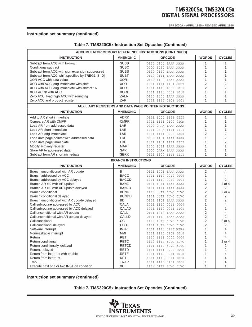
TMS320C5x, TMS320LC5xDIGITAL SIGNAL PROCESSORS
SPRS030A – APRIL 1995 – REVISED APRIL 1996
39POST OFFICE BOX 1443 • HOUSTON, TEXAS 77251–1443
instruction set summary (continued)
Table 7. TMS320C5x Instruction Set Opcodes (Continued)
ACCUMULATOR MEMORY REFERENCE INSTRUCTIONS (CONTINUED)
INSTRUCTION MNEMONIC OPCODE WORDS CYCLES
Subtract from ACC with borrowConditional subtractSubtract from ACC with sign extension suppressedSubtract from ACC, shift specified by TREG1 [3–0]XOR ACC with data valueXOR with ACC long immediate with shiftXOR with ACC long immediate with shift of 16XOR ACCB with ACCZero ACC, load high ACC with roundingZero ACC and product register
SUBBSUBCSUBSSUBTXORXORXORXORBZALRZAP
0110 0100 IAAA AAAA0000 1010 IAAA AAAA0110 0110 IAAA AAAA0110 0111 IAAA AAAA0110 1100 IAAA AAAA1011 1111 1101 SHFT1011 1110 1000 00111011 1110 0001 10100110 1000 IAAA AAAA1011 1110 0101 1001
1111122111
1111122111
AUXILIARY REGISTERS AND DATA PAGE POINTER INSTRUCTIONS
INSTRUCTION MNEMONIC OPCODE WORDS CYCLES
Add to AR short immediateCompare AR with CMPRLoad AR from addressed dataLoad AR short immediateLoad AR long immediateLoad data page pointer with addressed dataLoad data page immediateModify auxiliary registerStore AR to addressed dataSubtract from AR short immediate
ADRKCMPRLARLARLARLDPLDPMARSARSBRK
0111 1000 IIII IIII1011 1111 0100 01CM0000 0ARX IAAA AAAA1011 0ARX IIII IIII1011 1111 0000 1ARX0000 1101 IAAA AAAA1011 110I IIII IIII1000 1011 IAAA AAAA1000 0ARX IAAA AAAA0111 1100 IIII IIII
1111211111
1111222111
BRANCH INSTRUCTIONS
INSTRUCTION MNEMONIC OPCODE WORDS CYCLES
Branch unconditional with AR updateBranch addressed by ACCBranch addressed by ACC delayedBranch AR ≠ 0 with AR updateBranch AR ≠ 0 with AR update delayedBranch conditionalBranch conditional delayedBranch unconditional with AR update delayedCall subroutine addressed by ACCCall subroutine addressed by ACC delayedCall unconditional with AR updateCall unconditional with AR update delayedCall conditionalCall conditional delayedSoftware interruptNonmaskable interruptReturnReturn conditionalReturn conditionally, delayedReturn, delayedReturn from interrupt with enableReturn from interruptTrapExecute next one or two INST on condition
BBACCBACCDBANZBANZDBCNDBCNDDBDCALACALADCALLCALLDCCCCDINTRNMIRETRETCRETCDRETDRETERETITRAPXC
0111 1001 1AAA AAAA1011 1110 0010 00001011 1110 0010 00010111 1011 1AAA AAAA0111 1111 1AAA AAAA1110 00TP ZLVC ZLVC1111 00TP ZLVC ZLVC0111 1101 1AAA AAAA1011 1110 0011 00001011 1110 0011 11010111 1010 1AAA AAAA0111 1110 1AAA AAAA1110 10TP ZLVC ZLVC1111 10TP ZLVC ZLVC1011 1110 011 I NTR#1011 1110 0101 00101110 1111 0000 00001110 11TP ZLVC ZLVC1111 11TP ZLVC ZLVC1111 1111 0000 00001011 1110 0011 10101011 1110 0011 10001011 1110 0101 0001111N 01TP ZLVC ZLVC
211222221122221111111111
442
2 or 42
2 or 4224242
2 or 42444
2 or 4224441
instruction set summary (continued)
Table 7. TMS320C5x Instruction Set Opcodes (Continued)
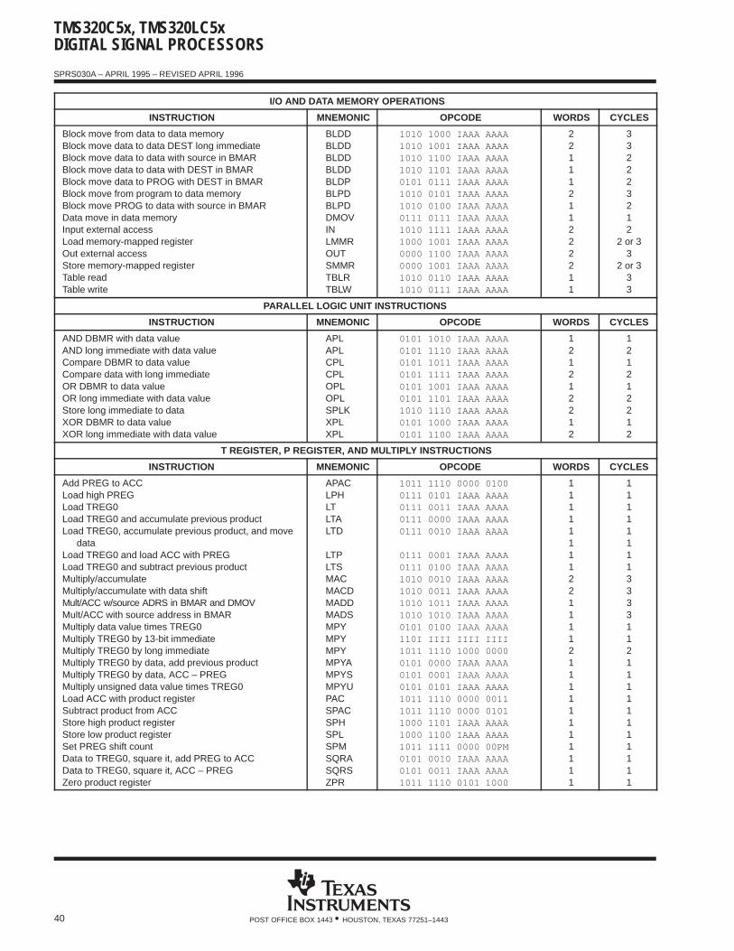
TMS320C5x, TMS320LC5xDIGITAL SIGNAL PROCESSORS
SPRS030A – APRIL 1995 – REVISED APRIL 1996
40 POST OFFICE BOX 1443 • HOUSTON, TEXAS 77251–1443
I/O AND DATA MEMORY OPERATIONS
INSTRUCTION MNEMONIC OPCODE WORDS CYCLES
Block move from data to data memoryBlock move data to data DEST long immediateBlock move data to data with source in BMARBlock move data to data with DEST in BMARBlock move data to PROG with DEST in BMARBlock move from program to data memoryBlock move PROG to data with source in BMARData move in data memoryInput external accessLoad memory-mapped registerOut external accessStore memory-mapped registerTable readTable write
BLDDBLDDBLDDBLDDBLDPBLPDBLPDDMOVINLMMROUTSMMRTBLRTBLW
1010 1000 IAAA AAAA1010 1001 IAAA AAAA1010 1100 IAAA AAAA1010 1101 IAAA AAAA0101 0111 IAAA AAAA1010 0101 IAAA AAAA1010 0100 IAAA AAAA0111 0111 IAAA AAAA1010 1111 IAAA AAAA1000 1001 IAAA AAAA0000 1100 IAAA AAAA0000 1001 IAAA AAAA1010 0110 IAAA AAAA1010 0111 IAAA AAAA
22111211222211
332223212
2 or 33
2 or 333
PARALLEL LOGIC UNIT INSTRUCTIONS
INSTRUCTION MNEMONIC OPCODE WORDS CYCLES
AND DBMR with data valueAND long immediate with data valueCompare DBMR to data valueCompare data with long immediateOR DBMR to data valueOR long immediate with data valueStore long immediate to dataXOR DBMR to data valueXOR long immediate with data value
APLAPLCPLCPLOPLOPLSPLKXPLXPL
0101 1010 IAAA AAAA0101 1110 IAAA AAAA0101 1011 IAAA AAAA0101 1111 IAAA AAAA0101 1001 IAAA AAAA 0101 1101 IAAA AAAA1010 1110 IAAA AAAA0101 1000 IAAA AAAA0101 1100 IAAA AAAA
121212212
121212212
T REGISTER, P REGISTER, AND MULTIPLY INSTRUCTIONS
INSTRUCTION MNEMONIC OPCODE WORDS CYCLES
Add PREG to ACCLoad high PREGLoad TREG0Load TREG0 and accumulate previous productLoad TREG0, accumulate previous product, and move
dataLoad TREG0 and load ACC with PREGLoad TREG0 and subtract previous productMultiply/accumulateMultiply/accumulate with data shiftMult/ACC w/source ADRS in BMAR and DMOVMult/ACC with source address in BMARMultiply data value times TREG0Multiply TREG0 by 13-bit immediateMultiply TREG0 by long immediateMultiply TREG0 by data, add previous productMultiply TREG0 by data, ACC – PREGMultiply unsigned data value times TREG0Load ACC with product registerSubtract product from ACCStore high product registerStore low product registerSet PREG shift countData to TREG0, square it, add PREG to ACCData to TREG0, square it, ACC – PREGZero product register
APACLPH LT LTALTD
LTPLTSMACMACDMADDMADSMPYMPYMPYMPYAMPYSMPYUPACSPACSPHSPLSPMSQRASQRSZPR
1011 1110 0000 01000111 0101 IAAA AAAA0111 0011 IAAA AAAA0111 0000 IAAA AAAA0111 0010 IAAA AAAA
0111 0001 IAAA AAAA0111 0100 IAAA AAAA1010 0010 IAAA AAAA1010 0011 IAAA AAAA1010 1011 IAAA AAAA1010 1010 IAAA AAAA0101 0100 IAAA AAAA110I IIII IIII IIII1011 1110 1000 00000101 0000 IAAA AAAA0101 0001 IAAA AAAA0101 0101 IAAA AAAA1011 1110 0000 00111011 1110 0000 01011000 1101 IAAA AAAA1000 1100 IAAA AAAA1011 1111 0000 00PM0101 0010 IAAA AAAA0101 0011 IAAA AAAA1011 1110 0101 1000
11111111221111211111111111
11111111333311211111111111
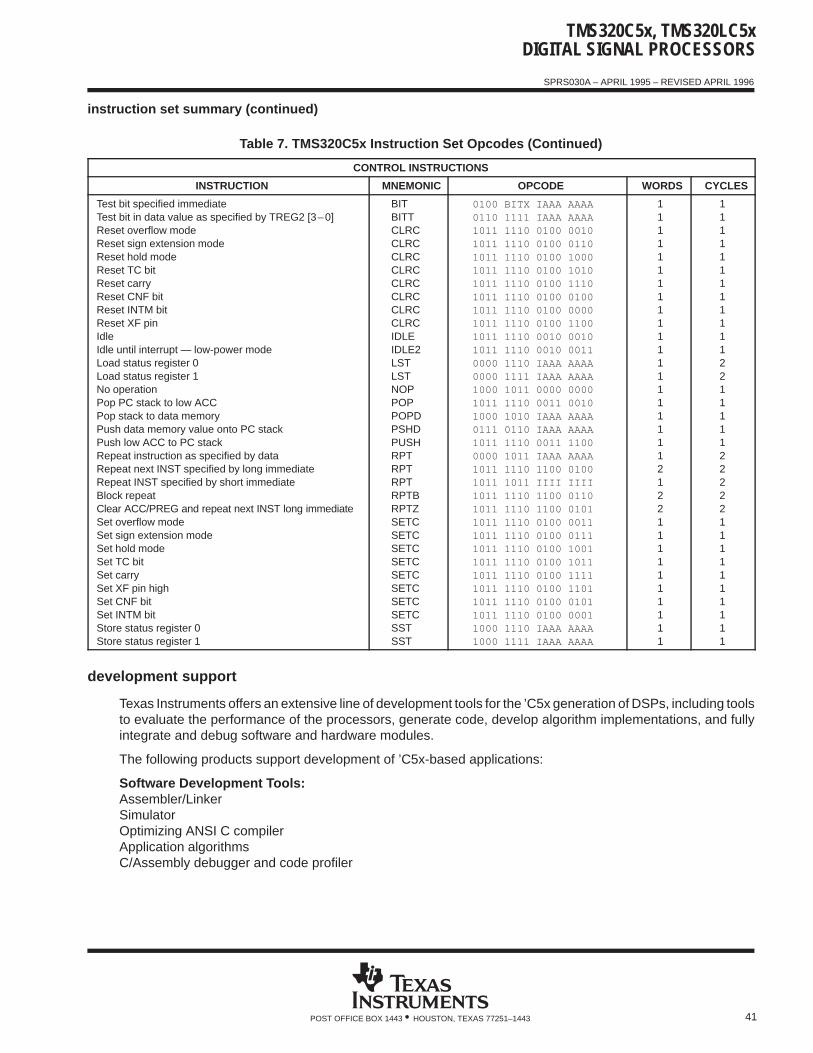
TMS320C5x, TMS320LC5xDIGITAL SIGNAL PROCESSORS
SPRS030A – APRIL 1995 – REVISED APRIL 1996
41POST OFFICE BOX 1443 • HOUSTON, TEXAS 77251–1443
instruction set summary (continued)
Table 7. TMS320C5x Instruction Set Opcodes (Continued)
CONTROL INSTRUCTIONS
INSTRUCTION MNEMONIC OPCODE WORDS CYCLES
Test bit specified immediateTest bit in data value as specified by TREG2 [3–0]Reset overflow modeReset sign extension modeReset hold modeReset TC bitReset carryReset CNF bitReset INTM bitReset XF pinIdleIdle until interrupt — low-power modeLoad status register 0Load status register 1No operationPop PC stack to low ACCPop stack to data memoryPush data memory value onto PC stackPush low ACC to PC stackRepeat instruction as specified by dataRepeat next INST specified by long immediateRepeat INST specified by short immediateBlock repeatClear ACC/PREG and repeat next INST long immediateSet overflow modeSet sign extension modeSet hold modeSet TC bitSet carrySet XF pin highSet CNF bitSet INTM bitStore status register 0Store status register 1
BITBITTCLRCCLRCCLRCCLRCCLRCCLRCCLRCCLRCIDLEIDLE2LSTLSTNOPPOPPOPDPSHDPUSHRPTRPTRPTRPTBRPTZSETCSETCSETCSETCSETCSETCSETCSETCSSTSST
0100 BITX IAAA AAAA0110 1111 IAAA AAAA1011 1110 0100 00101011 1110 0100 01101011 1110 0100 10001011 1110 0100 10101011 1110 0100 11101011 1110 0100 01001011 1110 0100 00001011 1110 0100 11001011 1110 0010 00101011 1110 0010 00110000 1110 IAAA AAAA0000 1111 IAAA AAAA1000 1011 0000 00001011 1110 0011 00101000 1010 IAAA AAAA0111 0110 IAAA AAAA1011 1110 0011 11000000 1011 IAAA AAAA1011 1110 1100 01001011 1011 IIII IIII1011 1110 1100 01101011 1110 1100 01011011 1110 0100 00111011 1110 0100 01111011 1110 0100 10011011 1110 0100 10111011 1110 0100 11111011 1110 0100 11011011 1110 0100 01011011 1110 0100 00011000 1110 IAAA AAAA1000 1111 IAAA AAAA
1111111111111111111121221111111111
1111111111112211111222221111111111
development support
Texas Instruments offers an extensive line of development tools for the ’C5x generation of DSPs, including toolsto evaluate the performance of the processors, generate code, develop algorithm implementations, and fullyintegrate and debug software and hardware modules.
The following products support development of ’C5x-based applications:
Software Development Tools:Assembler/LinkerSimulatorOptimizing ANSI C compilerApplication algorithmsC/Assembly debugger and code profiler
TMS320C5x, TMS320LC5xDIGITAL SIGNAL PROCESSORS
SPRS030A – APRIL 1995 – REVISED APRIL 1996
42 POST OFFICE BOX 1443 • HOUSTON, TEXAS 77251–1443
development support (continued)
Hardware Development Tools:Extended development set (XDS ) emulator (supports ’C5x multiprocessor system debug)’C5x EVM (Evaluation Module)’C5x DSK (DSP Starter Kit)
The TMS320 Family Development Support Reference Guide (SPRU011) contains information aboutdevelopment support products for all TMS320 family member devices, including documentation. Refer to thisdocument for further information about TMS320 documentation or any other TMS320 support products fromTexas Instruments. There is an additional document, the TMS320 Third Party Support Reference Guide(SPRU052), which contains information about TMS320-related products from other companies in the industry.To receive copies of TMS320 literature, contact the Literature Response Center at 800/477-8924.
See Table 8 for complete listings of development support tools for the ’C5x. For information on pricing andavailability, contact the nearest TI field sales office or authorized distributor.
Table 8. TMS320C5x, TMS320LC5x Development Support Tools
DEVELOPMENT TOOL PLATFORM PART NUMBER
Software
Compiler/Assembler/Linker PC-DOS , OS/2 TMDS3242855-02
Compiler/Assembler/Linker SPARC , HP TMDS3242555-08
Assembler/Linker PC-DOS, OS/2 TMDS3242850-02
Simulator PC-DOS, WIN TMDS3245851-02
Simulator SPARC TMDS3245551-09
Digital Filter Design Package PC-DOS DFDP
Debugger/Emulation Software PC-DOS, OS/2, WIN TMDS3240150
Debugger/Emulation Software SPARC TMDS3240650
Hardware
XDS-510 XL Emulator PC-DOS, OS/2 TMD000510
XDS-510 WS Emulator SPARC TMDS000510WS
EVM Evaluation Module PC-DOS, WIN TMDS3260050
DSK DSP Starter Kit PC-DOS TMDS3200051
device and development support tool nomenclature
To designate the stages in the product development cycle, TI assigns prefixes to the part numbers of all TMS320devices and support tools. Each TMS320 member has one of three prefixes: TMX, TMP, or TMS. TexasInstruments recommends two of three possible prefix designators for its support tools: TMDX and TMDS. Theseprefixes represent evolutionary stages of product development from engineering prototypes (TMX/TMDX)through fully qualified production devices/tools (TMS/TMDS). This development flow is defined below.
Device development evolutionary flow:
TMX Experimental device that is not necessarily representative of the final device’s electricalspecifications
TMP Final silicon die that conforms to the device’s electrical specifications but has not completedquality and reliability verification
PC-DOS and OS/2 are trademarks of International Business Machines Corp.SPARC is a trademark of SPARC International, Inc.WIN is a trademark of Microsoft Corporation.HP is a trademark of Hewlett-Packard Company.XDS is a trademark of Texas Instruments Incorporated.
TMS320C5x, TMS320LC5xDIGITAL SIGNAL PROCESSORS
SPRS030A – APRIL 1995 – REVISED APRIL 1996
43POST OFFICE BOX 1443 • HOUSTON, TEXAS 77251–1443
device and development support tool nomenclature (continued)
TMS Fully-qualified production device
Support tool development evolutionary flow:
TMDX Development support product that has not yet completed Texas Instruments internal qualificationtesting.
TMDS Fully qualified development support product
TMX and TMP devices and TMDX development support tools are shipped against the following disclaimer:
“Developmental product is intended for internal evaluation purposes.”
TMS devices and TMDS development support tools have been characterized fully, and the quality and reliabilityof the device has been demonstrated fully. TI’s standard warranty applies.
Predictions show that prototype devices (TMX or TMP) have a greater failure rate than the standard productiondevices. Texas Instruments recommends that these devices not be used in any production system because theirexpected end-use failure rate still is undefined. Only qualified production devices are to be used.
TI device nomenclature also includes a suffix with the device family name. This suffix indicates the package type(for example, N, FN, or GB) and temperature range (for example, L). Figure 8 provides a legend for reading thecomplete device name for any TMS320 family member.

TMS320C5x, TMS320LC5xDIGITAL SIGNAL PROCESSORS
SPRS030A – APRIL 1995 – REVISED APRIL 1996
44 POST OFFICE BOX 1443 • HOUSTON, TEXAS 77251–1443
PREFIX TEMPERATURE RANGE (DEFAULT: 0 TO 70 °C)
TMS 320 (B) 52 PJ (L)
TMX= experimental deviceTMP= prototype deviceTMS= qualified deviceSMJ = MIL-STD-883CSM = High Rel (non-883C)
DEVICE FAMILY320 = TMS320 Family
TECHNOLOGY
H = 0 to 50°CL = 0 to 70°CS = –55 to 100°CM = –55 to 125°CA = –40 to 85°C
PACKAGE TYPEN = plastic DIPJ = ceramic CER-DIPJD = ceramic DIP side-brazedGB = ceramic PGAFZ = ceramic CER-QUADFN = plastic leaded CCFD = ceramic leadless CCPJ = 100-pin plastic EIAJ QFPPQ = 132-pin plastic bumpered QFPPZ = 100-pin plastic TQFPPBK = 128-pin plastic TQFPPGE= 144-pin plastic TQFP
C = CMOSE = CMOS EPROM
DEVICE’C1x DSP:
1014151617
’C2x DSP:2526
’C2xx DSP:203209
’C3x DSP:303132
’C4x DSP:4044
’C5x DSP:505152535657
(L)
LOW VOLTAGE OPTION (3.3V)
BOOT LOADER OPTION
C
Figure 8. TMS320 Device Nomenclature
documentation support
Extensive documentation supports all TMS320 family generations of devices from product announcementthrough applications development. The types of documentation available include data sheets, such as thisdocument, with design specifications, complete user’s guides for all devices, development support tools, andthree volumes of the publication Digital Signal Processing Applications with the TMS320 Family (literaturenumbers SPRA012, SPRA016, and SPRA017).
The application book series describes hardware and software applications, including algorithms, for fixed andfloating point TMS320 family devices. The TMS320C5x User’s Guide (literature number SPRU056), whichdescribes in detail the fifth-generation TMS320 products, is currently available.
A series of DSP textbooks is published by Prentice-Hall and John Wiley & Sons to support digital signalprocessing research and education. The TMS320 newsletter, Details on Signal Processing, is publishedquarterly and distributed to update TMS320 customers on product information. The TMS320 DSP bulletin boardservice (BBS) provides access to information pertaining to the TMS320 family, including documentation, sourcecode and object code for many DSP algorithms and utilities. The BBS can be reached at 713/274-2323.
Information regarding TI DSP products is also available on the Worldwide Web at http:/www.ti.com uniformresource locator (URL).
TMS320C5x, TMS320LC5xDIGITAL SIGNAL PROCESSORS
SPRS030A – APRIL 1995 – REVISED APRIL 1996
45POST OFFICE BOX 1443 • HOUSTON, TEXAS 77251–1443
absolute maximum ratings over operating ambient-air temperature range (unless otherwise noted)(’320C5x only) †
Supply voltage range, VDD (see Note 3) – 0.3 V to 7 V. . . . . . . . . . . . . . . . . . . . . . . . . . . . . . . . . . . . . . . . . . . . . Input voltage range, VI – 0.3 V to 7 V. . . . . . . . . . . . . . . . . . . . . . . . . . . . . . . . . . . . . . . . . . . . . . . . . . . . . . . . . . . . . Output voltage range, VO – 0.3 V to 7 V. . . . . . . . . . . . . . . . . . . . . . . . . . . . . . . . . . . . . . . . . . . . . . . . . . . . . . . . . . Operating ambient temperature range, TA –40°C to 85°C. . . . . . . . . . . . . . . . . . . . . . . . . . . . . . . . . . . . . . . . . . . Operating case temperature, TC 0°C to 85°C. . . . . . . . . . . . . . . . . . . . . . . . . . . . . . . . . . . . . . . . . . . . . . . . . . . . . . Storage temperature range, Tstg – 55°C to 150°C. . . . . . . . . . . . . . . . . . . . . . . . . . . . . . . . . . . . . . . . . . . . . . . . . .
† Stresses beyond those listed under “absolute maximum ratings” may cause permanent damage to the device. These are stress ratings only, andfunctional operation of the device at these or any other conditions beyond those indicated under “recommended operating conditions” is notimplied. Exposure to absolute-maximum-rated conditions for extended periods may affect device reliability.
NOTE 3: All voltage values are with respect to VSS.
recommended operating conditions (’320C5x only)
MIN NOM MAX UNIT
VDD Supply voltage 4.75 5 5.25 V
VSS Supply voltage 0 V
X2/CLKIN, CLKIN2 3 VDD+0.3
VIH High-level input voltage CLKX, CLKR, TCLKX, TCLKR 2.5 VDD+0.3 V
All other inputs 2 VDD+0.3
VIL Low level input voltageX2/CLKIN, CLKIN2, CLKX, CLKR, TCLKX, TCLKR – 0.3 0.7
VVIL Low-level input voltageAll other inputs – 0.3 0.8
V
IOH High-level output current (see Note 4) – 300‡ µA
IOL Low-level output current 2 mA
TC Operating case temperature 0 85 °C
TA Operating ambient temperature –40 85 °C‡ This IOH can be exceeded when using a 1-kΩ pulldown resistor on the TDM serial port TADD output; however, this output still meets VOH
specifications under these conditions.NOTE 4: Figure 9 shows the test load circuit and Figure 10 and Figure 11 show the voltage reference levels.
TMS320C5x, TMS320LC5xDIGITAL SIGNAL PROCESSORS
SPRS030A – APRIL 1995 – REVISED APRIL 1996
46 POST OFFICE BOX 1443 • HOUSTON, TEXAS 77251–1443
electrical characteristics over recommended ranges of supply voltage and operating ambient-airtemperature (unless otherwise noted) (’320C5x only)
PARAMETER TEST CONDITIONS MIN TYP‡ MAX UNIT
VOH High-level output voltage (see Note 4) IOH = 300 µA 2.4 3 V
VOL Low-level output voltage (see Note 4) IOL = 2 mA 0.3 0.6 V
IOZ High impedance output current (VDD = 5 25 V)BR (with internal pullup) – 500 20
µAIOZ High-impedance output current (VDD = 5.25 V)All other 3-state outputs – 20 20
µA
TRST (with internal pulldown) – 10 800
II Input current (VI = VSS to VDD)TMS, TCK, TDI (with internal pullups) – 500 10
µAII Input current (VI = VSS to VDD)X2/CLKIN – 50 50
µA
All other inputs – 10 10
fx = 40 MHz, VDD = 5.25 V 60
IDD( ) Supply current core CPUfx = 57 MHz, VDD = 5.25 V 67
mAIDD(core) Supply current, core CPUfx = 80 MHz, VDD = 5.25 V 94
mA
fx = 100 MHz, VDD = 5.25 V 110
fx = 40 MHz, VDD = 5.25 V 40
IDD( i ) Supply current pinsfx = 57 MHz, VDD = 5.25 V 45
mAIDD(pins) Supply current, pinsfx = 80 MHz, VDD = 5.25 V 63
mA
fx = 100 MHz, VDD = 5.25 V 75
IDD(standby)Supply current, standbyIDLE2, divide-by-two clock mode, clocksshut off
5 µA
Ci Input capacitance 15 pF
Co Output capacitance 15 pF
† Typical values are at VDD = 5 V, TA = 25°C, unless otherwise specified.NOTE 4: Figure 9 shows the test load circuit and Figure 10 and Figure 11 show the voltage reference levels.
TMS320C5x, TMS320LC5xDIGITAL SIGNAL PROCESSORS
SPRS030A – APRIL 1995 – REVISED APRIL 1996
47POST OFFICE BOX 1443 • HOUSTON, TEXAS 77251–1443
absolute maximum ratings over specified temperature range (unless otherwise noted) (’320LC5xonly) †
Supply voltage range, VDD (see Note 3) –0.3 V to 5 V. . . . . . . . . . . . . . . . . . . . . . . . . . . . . . . . . . . . . . . . . . . . . . . Input voltage range, VI –0.3 V to 5 V. . . . . . . . . . . . . . . . . . . . . . . . . . . . . . . . . . . . . . . . . . . . . . . . . . . . . . . . . . . . . . Output voltage range, VO –0.3 V to 5 V. . . . . . . . . . . . . . . . . . . . . . . . . . . . . . . . . . . . . . . . . . . . . . . . . . . . . . . . . . . . Operating ambient temperature range, TA –40° to 85°C. . . . . . . . . . . . . . . . . . . . . . . . . . . . . . . . . . . . . . . . . . . . . Operating case temperature, TC 0°C to 85°C. . . . . . . . . . . . . . . . . . . . . . . . . . . . . . . . . . . . . . . . . . . . . . . . . . . . . . Storage temperature range, Tstg –55° to 150°C. . . . . . . . . . . . . . . . . . . . . . . . . . . . . . . . . . . . . . . . . . . . . . . . . . . . .
† Stresses beyond those listed under “absolute maximum ratings” may cause permanent damage to the device. These are stress ratings only, andfunctional operation of the device at these or any other conditions beyond those indicated in the “recommended operating conditions” is notimplied. Exposure to absolute-maximum-rated conditions for extended periods may affect device reliability.
NOTE 3: All voltage values are with respect to VSS.
recommended operating conditions (’320LC5x only)MIN NOM MAX UNIT
VDD Supply voltage 3.13 3.3 3.47 V
VSS Supply voltage 0 V
X2/CLKIN, CLKIN2 2.5 VDD + 0.3
VIH High-level input voltage CLKX, CLKR, TCLKX, TCLKR 2.0 VDD + 0.3 V
All other inputs 1.8 VDD + 0.3
VIL Low-level input voltage
X2/CLKIN, CLKIN2, CLKX,CLKR, TCLKX, TCLKR
–0.3 0.5 VIL o e e u o age
All other inputs –0.3 0.6 V
IOH High-level output current – 300‡ µA
IOL Low-level output current 2 mA
TC Operating case temperature 0 85 °C
TA Operating ambient temperature –40 85 °C‡ This IOH may be exceeded when using a 1-kΩ pulldown resistor on the TDM serial port TADD output; however, this output still meets VOH
specifications under these conditions.
TMS320C5x, TMS320LC5xDIGITAL SIGNAL PROCESSORS
SPRS030A – APRIL 1995 – REVISED APRIL 1996
48 POST OFFICE BOX 1443 • HOUSTON, TEXAS 77251–1443
electrical characteristics over recommended ranges of supply voltage and operating free-airtemperature (unless otherwise noted) (’320LC5x only)
PARAMETER TEST CONDITIONS MIN TYP† MAX UNIT
VOHHigh-level output voltage IOH = 300 µA 2.0
VVOHg g
(see Note 4) IOH = 20 µA VDD – 0.3‡V
VOLLow-level output voltage IOL = 2 mA 0.4
VVOLg
(see Note 4) IOL = 20 µA 0.3‡V
IHigh-impedance output current BR (with internal pullup) –500 20
AIOZHigh im edance out ut current(VDD = 3.47 V) All other 3-state outputs –20 20
µA
TRST(with internal pulldown) –10 800
TMS, TCK, TDI pins (with internal pullups) –500 10
II Input current (VI = VSS to VDD) X2/CLKIN (oscillator enabled) –50 50 µAI ( I SS DD)
X2/CLKIN (oscillator disabled) –10 10
µ
All other inputs –10 10
fx = 40 MHz, VDD = 3.47 V 26
IDD(core) Supply current, core CPU fx = 50 MHz, VDD = 3.47 V 33 mA( )fx = 80 MHz, VDD = 3.47 V 53
fx = 40 MHz, VDD = 3.47 V 18
IDD(pins) Supply current, pins fx = 50 MHz, VDD = 3.47 V 22 mA( )fx = 80 MHz, VDD = 3.47 V 35
IDD(standby) Supply current, standbyIDLE2, divide-by-two clock mode, clocksshut off
5 µA
Ci Input capacitance 15 pF
Co Output capacitance 15 pF
† All typical values are at VDD = 3.3 V, TA = 25°C.‡ Values derived from characterization data and not testedNOTE 4: Figure 9 shows the test load circuit and Figure 10 and Figure 11 show the voltage reference levels.
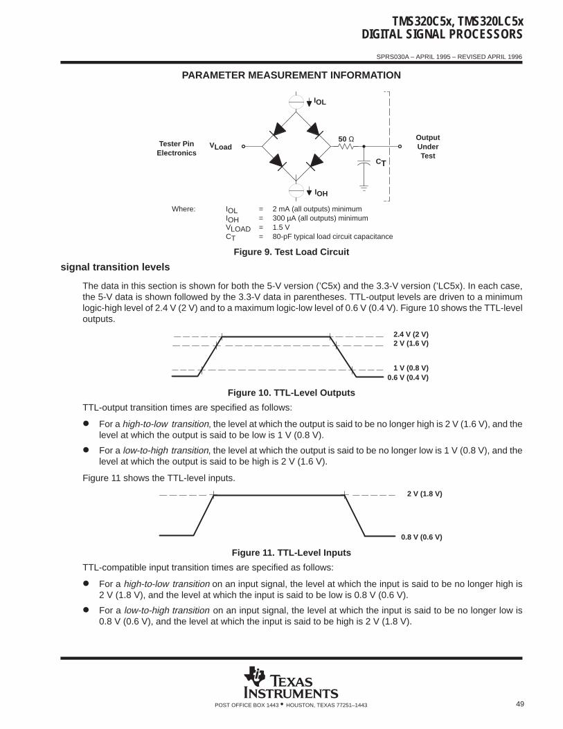
TMS320C5x, TMS320LC5xDIGITAL SIGNAL PROCESSORS
SPRS030A – APRIL 1995 – REVISED APRIL 1996
49POST OFFICE BOX 1443 • HOUSTON, TEXAS 77251–1443
PARAMETER MEASUREMENT INFORMATION
Tester PinElectronics
VLoad
IOL
CT
IOH
OutputUnderTest
50 Ω
Where: IOL = 2 mA (all outputs) minimumIOH = 300 µA (all outputs) minimumVLOAD = 1.5 VCT = 80-pF typical load circuit capacitance
Figure 9. Test Load Circuit
signal transition levels
The data in this section is shown for both the 5-V version (’C5x) and the 3.3-V version (’LC5x). In each case,the 5-V data is shown followed by the 3.3-V data in parentheses. TTL-output levels are driven to a minimumlogic-high level of 2.4 V (2 V) and to a maximum logic-low level of 0.6 V (0.4 V). Figure 10 shows the TTL-leveloutputs.
0.6 V (0.4 V)1 V (0.8 V)
2 V (1.6 V)2.4 V (2 V)
Figure 10. TTL-Level Outputs
TTL-output transition times are specified as follows:
For a high-to-low transition, the level at which the output is said to be no longer high is 2 V (1.6 V), and thelevel at which the output is said to be low is 1 V (0.8 V).
For a low-to-high transition, the level at which the output is said to be no longer low is 1 V (0.8 V), and thelevel at which the output is said to be high is 2 V (1.6 V).
Figure 11 shows the TTL-level inputs.
2 V (1.8 V)
0.8 V (0.6 V)
Figure 11. TTL-Level Inputs
TTL-compatible input transition times are specified as follows:
For a high-to-low transition on an input signal, the level at which the input is said to be no longer high is2 V (1.8 V), and the level at which the input is said to be low is 0.8 V (0.6 V).
For a low-to-high transition on an input signal, the level at which the input is said to be no longer low is0.8 V (0.6 V), and the level at which the input is said to be high is 2 V (1.8 V).
TMS320C5x, TMS320LC5xDIGITAL SIGNAL PROCESSORS
SPRS030A – APRIL 1995 – REVISED APRIL 1996
50 POST OFFICE BOX 1443 • HOUSTON, TEXAS 77251–1443
PARAMETER MEASUREMENT INFORMATION
timing parameter symbology
Timing parameter symbols used are created in accordance with JEDEC Standard 100-A. To shorten thesymbols, some of the pin names and other related terminology have been abbreviated as follows:
Lowercase subscripts and their meanings: Letters and symbols and their meanings:
a access time H High
c cycle time (period) L Low
d delay time V Valid
dis disable time Z High impedance
en enable time
f fall time
h hold time
r rise time
su setup time
t transition time
v valid time
w pulse duration (width)
X Unknown, changing, or don’t care level
TMS320C5x, TMS320LC5xDIGITAL SIGNAL PROCESSORS
SPRS030A – APRIL 1995 – REVISED APRIL 1996
51POST OFFICE BOX 1443 • HOUSTON, TEXAS 77251–1443
CLOCK CHARACTERISTICS AND TIMING
The ’C5x can use either its internal oscillator or an external frequency source for a clock. The clock mode isdetermined by the clock mode pins (CLKMD1, CLKMD2, and CLKMD3). Table 9 shows the standard clockoptions available on the ’C50, ’LC50, ’C51, ’LC51, ’C52, ’LC52, ’C53, ’LC53, ’C53S, and ’LC53S. For thesedevices, the CLKIN2 pin functions as the external frequency input when using the PLL options. An expandedset of clock options is shown in Table 10 and is available on the ’LC56, ’C57S, and ’LC57 devices. For thesedevices, X2/CLKIN functions as the external frequency input when using the PLL options.
Table 9. Standard Clock Options
CLKMD1 CLKMD2 CLOCK SOURCE
1 0 PLL clock generator option†
0 1 Reserved for test purposes
1 1 External divide-by-two option or internal divide-by-two clock optionwith an external crystal
0 0 External divide-by-two option with the internal oscillator disabled
† PLL multiply-by-one option on ’C50, ’C51, ’C53, ’C53S devices, PLL multiply-by-two option on ’C52 device
Table 10. PLL Clock Option for ’LC56, ’C57S, and ’LC57
CLKMD1 CLKMD2 CLKMD3 CLOCK SOURCE
0 0 0 PLL multiply-by-three
0 1 0 PLL multiply-by-four
1 0 0 PLL multiply-by-five
1 1 0 PLL multiply-by-nine
0 0 1 External divide-by-two option with oscillator disabled
0 1 1 PLL multiply-by-two
1 0 1 PLL multiply-by-one
1 1 1 External/Internal divide-by-two with oscillator enabled
TMS320C5x, TMS320LC5xDIGITAL SIGNAL PROCESSORS
SPRS030A – APRIL 1995 – REVISED APRIL 1996
52 POST OFFICE BOX 1443 • HOUSTON, TEXAS 77251–1443
internal divide-by-two clock option with external crystal
The internal oscillator is enabled by connecting a crystal across X1 and X2/CLKIN. The frequency of CLKOUT1is one-half of the crystal’s oscillating frequency. The crystal should be in either fundamental or overtoneoperation and parallel resonant, with an effective series resistance of 30 Ω and a power dissipation of 1 mW;it should be specified at a load capacitance of 20 pF. Overtone crystals require an additional tuned-LC circuit.Figure 12 shows an external crystal (fundamental frequency) connected to the on-chip oscillator.
recommended operating conditions for internal divide-by-two clock option
MIN NOM MAX UNIT
TMS320C5x-40 0† 40.96
TMS320C5x-57 0† 57.14MHz
TMS320C5x-80 0† 80MHz
fclk Input clock frequency TMS320C5x-100‡ 0† 100
TMS320LC5x-40 0† 40
TMS320LC5x-50 0† 50 MHz
TMS320LC5x-80 0† 80
C1, C2 Load capacitance 10 pF
† This device utilizes a fully static design and, therefore, can operate with input clock cycle time (tc(CI)) approaching ∞. The device is characterizedat frequencies approaching 0 Hz, but is tested at fclk = 6.7 MHz to meet device test time requirements.
‡ ’320C51, ’320C52 currently available at this clock speed
X1 X2/CLKIN
C1 C2
Crystal
Figure 12. Internal Clock Option
TMS320C5x, TMS320LC5xDIGITAL SIGNAL PROCESSORS
SPRS030A – APRIL 1995 – REVISED APRIL 1996
53POST OFFICE BOX 1443 • HOUSTON, TEXAS 77251–1443
external divide-by-two clock option
An external frequency source can be used by injecting the frequency directly into X2/CLKIN with X1 leftunconnected. Refer to Table 9 and Table 10 for appropriate configuration of the CLKMD1, CLKMD2 andCLKMD3 pins to generate the external divide-by-2 clock option. The external frequency injected must conformto the specifications listed in the timing requirements table.
switching characteristics over recommended operating conditions [H = 0.5 t c(CO) ] (’320C5x only)(see Figure 13)
PARAMETER’320C5x-40 ’320C5x-57
UNITPARAMETERMIN TYP MAX MIN TYP MAX
UNIT
tc(CO) Cycle time, CLKOUT1 48.8 2tc(CI) † 35 2tc(CI) † ns
td(CIH-COH/L) Delay time, X2/CLKIN high to CLKOUT1 high / low 3 11 20 3 11 20 ns
tf(CO) Fall time, CLKOUT1 5 5 ns
tr(CO) Rise time, CLKOUT1 5 5 ns
tw(COL) Pulse duration, CLKOUT1 low H – 3 H H + 2 H – 3 H H + 2 ns
tw(COH) Pulse duration, CLKOUT1 high H – 3 H H + 2 H – 3 H H + 2 ns
PARAMETER’320C5x-80 ’320C5x-100
UNITPARAMETERMIN TYP MAX MIN TYP MAX
UNIT
tc(CO) Cycle time, CLKOUT1 25 2tc(CI) † 20 2tc(CI) † ns
td(CIH-COH/L) Delay time, X2/CLKIN high to CLKOUT1 high / low 1 9 18 1 9 18 ns
tf(CO) Fall time, CLKOUT1 4 4 ns
tr(CO) Rise time, CLKOUT1 4 4 ns
tw(COL) Pulse duration, CLKOUT1 low H – 3 H H + 2 H – 3 H H + 2 ns
tw(COH) Pulse duration, CLKOUT1 high H – 3 H H + 2 H – 3 H H + 2 ns
switching characteristics over recommended operating conditions [H = 0.5 t c(CO) ] (’320LC5x only)(see Figure 13)
PARAMETER’320LC5x-40 ’320LC5x-50 ’320LC5x-80 UNIT
PARAMETERMIN TYP MAX MIN TYP MAX MIN TYP MAX UNIT
tc(CO) Cycle time, CLKOUT1 50 2tc(CI) † 40 2tc(CI) † 25 2tc(CI) † ns
td(CIH-COH/L)Delay time, X2/CLKIN high toCLKOUT1 high / low
3 11 20 3 11 20 1 9 18 ns
tf(CO) Fall time, CLKOUT1 5 5 4 ns
tr(CO) Rise time, CLKOUT1 5 5 4 ns
tw(COL) Pulse duration, CLKOUT1 low H – 3 H H + 2 H – 3 H H + 2 H – 3 H H + 2 ns
tw(COH) Pulse duration, CLKOUT1 high H – 3 H H + 2 H – 3 H H + 2 H – 3 H H + 2 ns
† This device utilizes a fully static design and, therefore, can operate with tc(Cl) approaching infinity. The device is characterized at frequenciesapproaching 0 Hz but is tested at tc(CO) = 300 ns to meet device test time requirements.
TMS320C5x, TMS320LC5xDIGITAL SIGNAL PROCESSORS
SPRS030A – APRIL 1995 – REVISED APRIL 1996
54 POST OFFICE BOX 1443 • HOUSTON, TEXAS 77251–1443
timing requirements over recommended ranges of supply voltage and operating ambient-airtemperature (’320C5x only) (see Figure 13)
’320C5x-40 ’320C5x-57 ’320C5x-80 ’320C5x-100UNIT
MIN MAX MIN MAX MIN MAX MIN MAXUNIT
tc(CI) Cycle time, X2/CLKIN 24.4 † 17.5 † 12.5 † 10 † ns
tf(CI) Fall time, X2/CLKIN‡ 5 5 4 4 ns
tr(CI) Rise time, X2/CLKIN‡ 5 5 4 4 ns
tw(CIL) Pulse duration, X2/CLKIN low 11 † 8 † 5 † 5 † ns
tw(CIH) Pulse duration, X2/CLKIN high 11 † 8 † 5 † 5 † ns
timing requirements over recommended ranges of supply voltage and operating ambient-airtemperature (’320LC5x only) (see Figure 13)
’320LC5x-40 ’320LC5x-50 ’320LC5x-80UNIT
MIN MAX MIN MAX MIN MAXUNIT
tc(CI) Cycle time, X2/CLKIN 25 † 20 † 12.5 † ns
tf(CI) Fall time, X2/CLKIN‡ 5 5 4 ns
tr(CI) Rise time, X2/CLKIN‡ 5 5 4 ns
tw(CIL) Pulse duration, X2/CLKIN low 11 † 9 † 5 † ns
tw(CIH) Pulse duration, X2/CLKIN high 11 † 9 † 5 † ns
† This device utilizes a fully static design and, therefore, can operate with tc(Cl) approaching ∞. The device is characterized at frequenciesapproaching 0 Hz, but is tested at a minimum of tc(Cl) = 150 ns to meet device test time requirements.
‡ Values derived from characterization data and not tested
tr(CO)
tf(CO)
tw(COH)
CLKOUT1
CLKIN
tw(COL)td(CIH-COH/L)
tf(CI)tr(CI)
tw(CIL)tw(CIH)
tc(CO)
tc(CI)
Figure 13. External Divide-by-Two Clock Timing
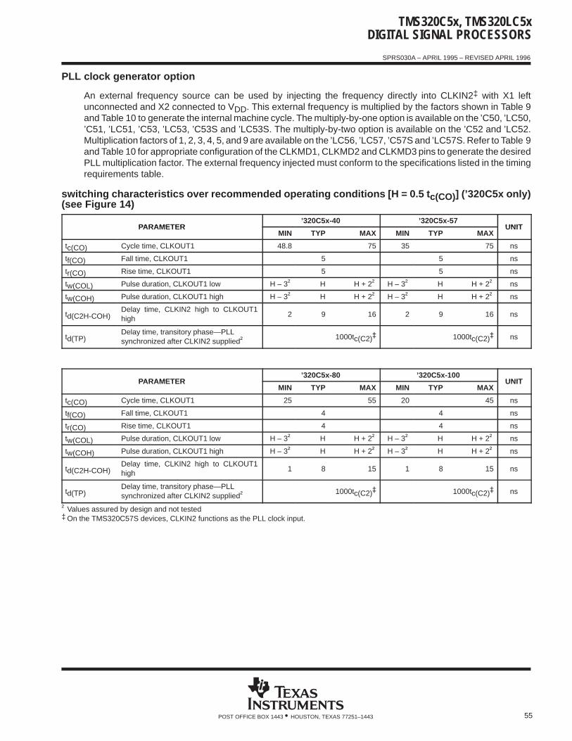
TMS320C5x, TMS320LC5xDIGITAL SIGNAL PROCESSORS
SPRS030A – APRIL 1995 – REVISED APRIL 1996
55POST OFFICE BOX 1443 • HOUSTON, TEXAS 77251–1443
PLL clock generator option
An external frequency source can be used by injecting the frequency directly into CLKIN2‡ with X1 leftunconnected and X2 connected to VDD. This external frequency is multiplied by the factors shown in Table 9and Table 10 to generate the internal machine cycle. The multiply-by-one option is available on the ’C50, ’LC50,’C51, ’LC51, ’C53, ’LC53, ’C53S and ’LC53S. The multiply-by-two option is available on the ’C52 and ’LC52.Multiplication factors of 1, 2, 3, 4, 5, and 9 are available on the ’LC56, ’LC57, ’C57S and ’LC57S. Refer to Table 9and Table 10 for appropriate configuration of the CLKMD1, CLKMD2 and CLKMD3 pins to generate the desiredPLL multiplication factor. The external frequency injected must conform to the specifications listed in the timingrequirements table.
switching characteristics over recommended operating conditions [H = 0.5 t c(CO)] (’320C5x only)(see Figure 14)
PARAMETER’320C5x-40 ’320C5x-57
UNITPARAMETERMIN TYP MAX MIN TYP MAX
UNIT
tc(CO) Cycle time, CLKOUT1 48.8 75 35 75 ns
tf(CO) Fall time, CLKOUT1 5 5 ns
tr(CO) Rise time, CLKOUT1 5 5 ns
tw(COL) Pulse duration, CLKOUT1 low H – 3† H H + 2† H – 3† H H + 2† ns
tw(COH) Pulse duration, CLKOUT1 high H – 3† H H + 2† H – 3† H H + 2† ns
td(C2H-COH)Delay time, CLKIN2 high to CLKOUT1high
2 9 16 2 9 16 ns
td(TP)Delay time, transitory phase—PLLsynchronized after CLKIN2 supplied† 1000tc(C2) 1000tc(C2) ns
PARAMETER’320C5x-80 ’320C5x-100
UNITPARAMETERMIN TYP MAX MIN TYP MAX
UNIT
tc(CO) Cycle time, CLKOUT1 25 55 20 45 ns
tf(CO) Fall time, CLKOUT1 4 4 ns
tr(CO) Rise time, CLKOUT1 4 4 ns
tw(COL) Pulse duration, CLKOUT1 low H – 3† H H + 2† H – 3† H H + 2† ns
tw(COH) Pulse duration, CLKOUT1 high H – 3† H H + 2† H – 3† H H + 2† ns
td(C2H-COH)Delay time, CLKIN2 high to CLKOUT1high
1 8 15 1 8 15 ns
td(TP)Delay time, transitory phase—PLLsynchronized after CLKIN2 supplied† 1000tc(C2) 1000tc(C2) ns
† Values assured by design and not tested‡ On the TMS320C57S devices, CLKIN2 functions as the PLL clock input.
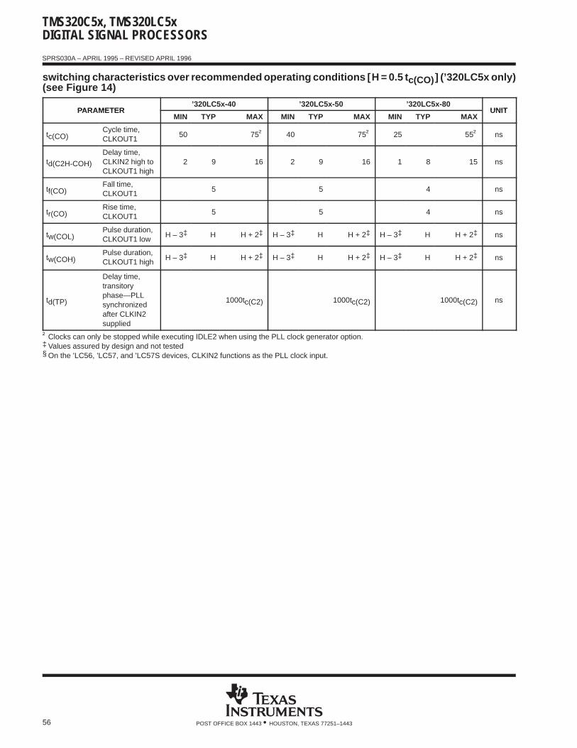
TMS320C5x, TMS320LC5xDIGITAL SIGNAL PROCESSORS
SPRS030A – APRIL 1995 – REVISED APRIL 1996
56 POST OFFICE BOX 1443 • HOUSTON, TEXAS 77251–1443
switching characteristics over recommended operating conditions [H = 0.5 t c(CO) ] (’320LC5x only)(see Figure 14)
PARAMETER’320LC5x-40 ’320LC5x-50 ’320LC5x-80
UNITPARAMETERMIN TYP MAX MIN TYP MAX MIN TYP MAX
UNIT
tc(CO)Cycle time,CLKOUT1
50 75† 40 75† 25 55† ns
td(C2H-COH)
Delay time,CLKIN2 high toCLKOUT1 high
2 9 16 2 9 16 1 8 15 ns
tf(CO)Fall time,CLKOUT1
5 5 4 ns
tr(CO)Rise time,CLKOUT1
5 5 4 ns
tw(COL)Pulse duration, CLKOUT1 low
H – 3‡ H H + 2‡ H – 3‡ H H + 2‡ H – 3‡ H H + 2‡ ns
tw(COH)Pulse duration, CLKOUT1 high
H – 3‡ H H + 2‡ H – 3‡ H H + 2‡ H – 3‡ H H + 2‡ ns
td(TP)
Delay time,transitoryphase—PLLsynchronizedafter CLKIN2supplied
1000tc(C2) 1000tc(C2) 1000tc(C2) ns
† Clocks can only be stopped while executing IDLE2 when using the PLL clock generator option.‡ Values assured by design and not tested§ On the ’LC56, ’LC57, and ’LC57S devices, CLKIN2 functions as the PLL clock input.
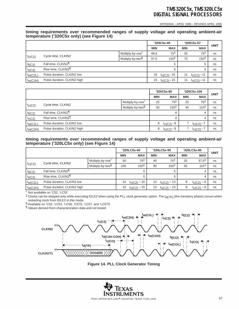
TMS320C5x, TMS320LC5xDIGITAL SIGNAL PROCESSORS
SPRS030A – APRIL 1995 – REVISED APRIL 1996
57POST OFFICE BOX 1443 • HOUSTON, TEXAS 77251–1443
timing requirements over recommended ranges of supply voltage and operating ambient-airtemperature (’320C5x only) (see Figure 14)
’320C5x-40 ’320C5x-57UNIT
MIN MAX MIN MAXUNIT
t (C2) Cycle time CLKIN2Multiply-by-one† 48.8 75‡ 35 75‡ ns
tc(C2) Cycle time, CLKIN2Multiply-by-two§ 97.6 150‡ 70 150‡ ns
tf(C2) Fall time, CLKIN2¶ 5 5 ns
tr(C2) Rise time, CLKIN2¶ 5 5 ns
tw(C2L) Pulse duration, CLKIN2 low 15 tc(C2)–15 11 tc(C2)–11 ns
tw(C2H) Pulse duration, CLKIN2 high 15 tc(C2)–15 11 tc(C2)–11 ns
’320C5x-80 ’320C5x-100UNIT
MIN MAX MIN MAXUNIT
t (C2) Cycle time CLKIN2Multiply-by-one† 25 75‡ 20 75‡ ns
tc(C2) Cycle time, CLKIN2Multiply-by-two§ 50 150‡ 40 110‡ ns
tf(C2) Fall time, CLKIN2¶ 4 4 ns
tr(C2) Rise time, CLKIN2¶ 4 4 ns
tw(C2L) Pulse duration, CLKIN2 low 8 tc(C2)–8 7 tc(C2)–7 ns
tw(C2H) Pulse duration, CLKIN2 high 8 tc(C2)–8 7 tc(C2)–7 ns
timing requirements over recommended ranges of supply voltage and operating ambient-airtemperature (’320LC5x only) (see Figure 14)
’320LC5x-40 ’320LC5x-50 ’320LC5x-80UNIT
MIN MAX MIN MAX MIN MAXUNIT
t (C2) Cycle time CLKIN2Multiply-by-one† 50 75‡ 40 75‡ 25 37.5‡ ns
tc(C2) Cycle time, CLKIN2Multiply-by-two§ 100 150‡ 80 150‡ 50 110‡ ns
tf(C2) Fall time, CLKIN2¶ 5 5 4 ns
tr(C2) Rise time, CLKIN2¶ 5 5 4 ns
tw(C2L) Pulse duration, CLKIN2 low 15 tc(C2) – 15 13 tc(C2) – 13 8 tc(C2) – 8 ns
tw(C2H) Pulse duration, CLKIN2 high 15 tc(C2) – 15 13 tc(C2) – 13 8 tc(C2) – 8 ns
† Not available on ’C52, ’LC52‡ Clocks can be stopped only while executing IDLE2 when using the PLL clock generator option. The td(TP) (the transitory phase) occurs when
restarting clock from IDLE2 in this mode.§ Available on ’C52, ’LC52, ’LC56, ’C57S, ’LC57, and ’LC57S¶ Values derived from characterization data and not tested
tr(C2)tw(C2L)tw(C2H)
td(TP)
tc(CO)
tc(C2)
tw(COH) tf(CO)tr(CO)
tf(C2)
CLKIN2
CLKOUT1
td(C2H-COH)
tw(COL)
Unstable
Figure 14. PLL Clock Generator Timing
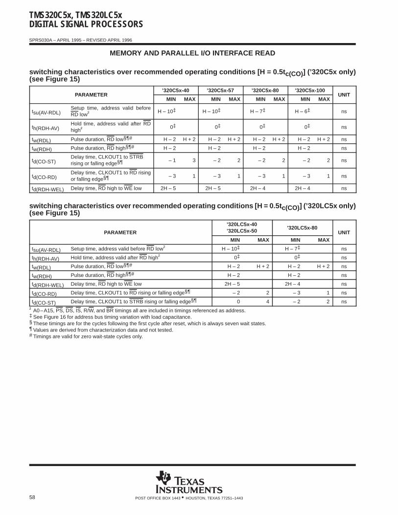
TMS320C5x, TMS320LC5xDIGITAL SIGNAL PROCESSORS
SPRS030A – APRIL 1995 – REVISED APRIL 1996
58 POST OFFICE BOX 1443 • HOUSTON, TEXAS 77251–1443
MEMORY AND PARALLEL I/O INTERFACE READ
switching characteristics over recommended operating conditions [H = 0.5t c(CO)] (’320C5x only)(see Figure 15)
PARAMETER’320C5x-40 ’320C5x-57 ’320C5x-80 ’320C5x-100
UNITPARAMETERMIN MAX MIN MAX MIN MAX MIN MAX
UNIT
tsu(AV-RDL)Setup time, address valid beforeRD low† H – 10‡ H – 10‡ H – 7‡ H – 6‡ ns
th(RDH-AV)Hold time, address valid after RDhigh† 0‡ 0‡ 0‡ 0‡ ns
tw(RDL) Pulse duration, RD low§¶# H – 2 H + 2 H – 2 H + 2 H – 2 H + 2 H – 2 H + 2 ns
tw(RDH) Pulse duration, RD high§¶# H – 2 H – 2 H – 2 H – 2 ns
td(CO-ST)Delay time, CLKOUT1 to STRB rising or falling edge§¶ – 1 3 – 2 2 – 2 2 – 2 2 ns
td(CO-RD)Delay time, CLKOUT1 to RD risingor falling edge§¶ – 3 1 – 3 1 – 3 1 – 3 1 ns
td(RDH-WEL) Delay time, RD high to WE low 2H – 5 2H – 5 2H – 4 2H – 4 ns
switching characteristics over recommended operating conditions [H = 0.5t c(CO)] (’320LC5x only)(see Figure 15)
PARAMETER
’320LC5x-40’320LC5x-50 ’320LC5x-80
UNITMIN MAX MIN MAX
tsu(AV-RDL) Setup time, address valid before RD low† H – 10‡ H – 7‡ ns
th(RDH-AV) Hold time, address valid after RD high† 0‡ 0‡ ns
tw(RDL) Pulse duration, RD low§¶# H – 2 H + 2 H – 2 H + 2 ns
tw(RDH) Pulse duration, RD high§¶# H – 2 H – 2 ns
td(RDH-WEL) Delay time, RD high to WE low 2H – 5 2H – 4 ns
td(CO-RD) Delay time, CLKOUT1 to RD rising or falling edge§¶ – 2 2 – 3 1 ns
td(CO-ST) Delay time, CLKOUT1 to STRB rising or falling edge§¶ 0 4 – 2 2 ns
† A0–A15, PS, DS, IS, R/W, and BR timings all are included in timings referenced as address.‡ See Figure 16 for address bus timing variation with load capacitance.§ These timings are for the cycles following the first cycle after reset, which is always seven wait states.¶ Values are derived from characterization data and not tested.# Timings are valid for zero wait-state cycles only.
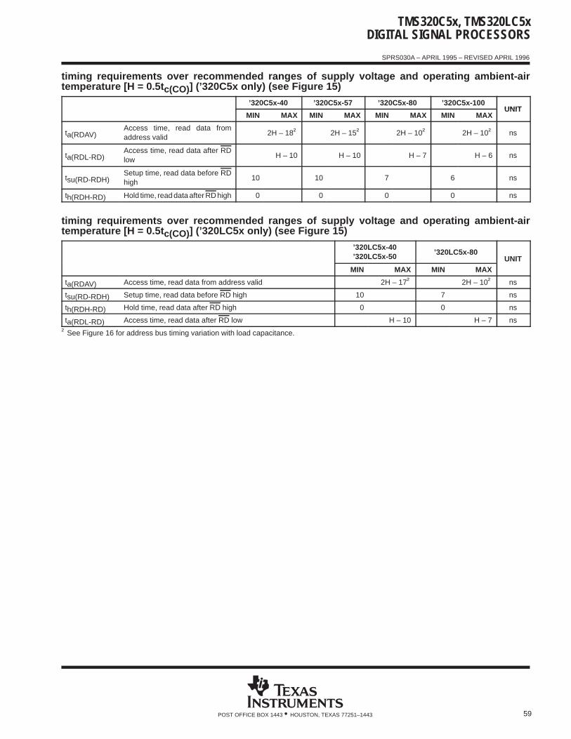
TMS320C5x, TMS320LC5xDIGITAL SIGNAL PROCESSORS
SPRS030A – APRIL 1995 – REVISED APRIL 1996
59POST OFFICE BOX 1443 • HOUSTON, TEXAS 77251–1443
timing requirements over recommended ranges of supply voltage and operating ambient-airtemperature [H = 0.5t c(CO)] (’320C5x only) (see Figure 15)
’320C5x-40 ’320C5x-57 ’320C5x-80 ’320C5x-100UNIT
MIN MAX MIN MAX MIN MAX MIN MAXUNIT
ta(RDAV)Access time, read data fromaddress valid
2H – 18† 2H – 15† 2H – 10† 2H – 10† ns
ta(RDL-RD)Access time, read data after RDlow
H – 10 H – 10 H – 7 H – 6 ns
tsu(RD-RDH)Setup time, read data before RDhigh
10 10 7 6 ns
th(RDH-RD) Hold time, read data after RD high 0 0 0 0 ns
timing requirements over recommended ranges of supply voltage and operating ambient-airtemperature [H = 0.5t c(CO)] (’320LC5x only) (see Figure 15)
’320LC5x-40’320LC5x-50 ’320LC5x-80
UNITMIN MAX MIN MAX
ta(RDAV) Access time, read data from address valid 2H – 17† 2H – 10† ns
tsu(RD-RDH) Setup time, read data before RD high 10 7 ns
th(RDH-RD) Hold time, read data after RD high 0 0 ns
ta(RDL-RD) Access time, read data after RD low H – 10 H – 7 ns
† See Figure 16 for address bus timing variation with load capacitance.
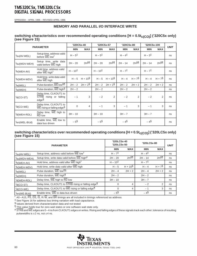
TMS320C5x, TMS320LC5xDIGITAL SIGNAL PROCESSORS
SPRS030A – APRIL 1995 – REVISED APRIL 1996
60 POST OFFICE BOX 1443 • HOUSTON, TEXAS 77251–1443
MEMORY AND PARALLEL I/O INTERFACE WRITE
switching characteristics over recommended operating conditions [H = 0.5t c(CO)] (’320C5x only)(see Figure 15)
PARAMETER’320C5x-40 ’320C5x-57 ’320C5x-80 ’320C5x-100
UNITPARAMETERMIN MAX MIN MAX MIN MAX MIN MAX
UNIT
tsu(AV-WEL)Setup time, address validbefore WE low† H – 5‡ H – 5‡ H – 4‡ H – 3‡ ns
tsu(WDV-WEH)Setup time, write datavalid before WE high
2H – 20 2H§¶ 2H – 20 2H§¶ 2H – 14 2H§¶ 2H – 14 2H§¶ ns
th(WEH-AV)Hold time, address valid after WE high† H – 10‡ H – 10‡ H – 7‡ H – 7‡ ns
th(WEH-WDV)Hold time, write data validafter WE high
H – 5 H + 10§ H – 5 H + 10§ H – 4 H + 7§ H – 4 H + 7§ ns
tw(WEL) Pulse duration, WE low§¶ 2H – 2 2H + 2§ 2H – 2 2H + 2§ 2H – 2 2H + 2 2H – 2 2H + 2 ns
tw(WEH) Pulse duration, WE high§ 2H – 2 2H – 2 2H – 2 2H – 2 ns
td(CO-ST)
Delay time, CLKOUT1 toSTRB rising or fallingedge§
– 1 3 – 2 2 – 2 2 – 2 2 ns
td(CO-WE)Delay time, CLKOUT1 toWE rising or falling edge§ 0 4 – 1 3 – 1 3 – 1 3 ns
td(WEH-RDL)Delay time, WE high toRD low
3H – 10 3H – 10 3H – 7 3H – 7 ns
ten(WEL-BUd)Enable time, WE low todata bus driven
– 5§ – 5§ – 4§ – 4§ ns
switching characteristics over recommended operating conditions [H = 0.5t c(CO)] (’320LC5x only)(see Figure 15)
PARAMETER
’320LC5x-40’320LC5x-50 ’320LC5x-80
UNITMIN MAX MIN MAX
tsu(AV-WEL) Setup time, address valid before WE low† H – 7‡ H – 4‡ ns
tsu(WDV-WEH) Setup time, write data valid before WE high# 2H – 20 2H§¶ 2H – 14 2H§¶ ns
th(WEH-AV) Hold time, address valid after WE high† H – 10‡ H – 7‡ ns
th(WEH-WDV) Hold time, write data valid after WE high H – 5 H + 10§ H – 4 H + 7§ ns
tw(WEL) Pulse duration, WE low¶§ 2H – 4 2H + 2 2H – 4 2H + 2 ns
tw(WEH) Pulse duration, WE high¶ 2H – 2 2H – 2 ns
td(WEH-RDL) Delay time, WE high to RD low 3H – 10 3H – 7 ns
td(CO-ST) Delay time, CLKOUT1 to STRB rising or falling edge¶ 0 4 – 2 2 ns
td(CO-WE) Delay time, CLKOUT1 to WE rising or falling edge¶ 0 4 – 1 3 ns
ten(WE-BUd) Enable time, WE to data bus driven – 5§ – 4§ ns
† A0–A15, PS, DS, IS, R /W, and BR timings are all included in timings referenced as address.‡ See Figure 16 for address bus timing variation with load capacitance.§ Values derived from characterization data and not tested¶ This value holds true for zero wait states or one software wait state only.# STRB and WE edges are 0–4 ns from CLKOUT1 edges on writes. Rising and falling edges of these signals track each other; tolerance of resulting
pulsewidths is ±2 ns, not ±4 ns.
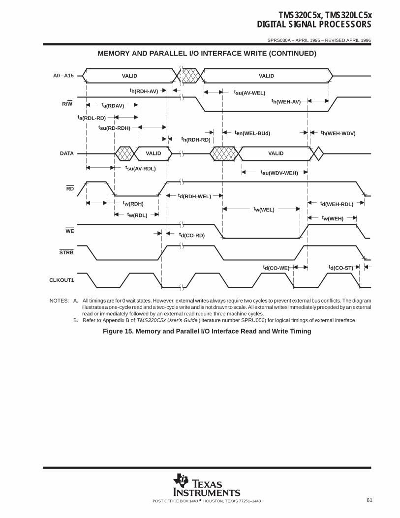
TMS320C5x, TMS320LC5xDIGITAL SIGNAL PROCESSORS
SPRS030A – APRIL 1995 – REVISED APRIL 1996
61POST OFFICE BOX 1443 • HOUSTON, TEXAS 77251–1443
MEMORY AND PARALLEL I/O INTERFACE WRITE (CONTINUED)
th(RDH-AV) tsu(AV-WEL)th(WEH-AV)
th(WEH-WDV)ten(WEL-BUd)th(RDH-RD)
ta(RDAV)
tsu(AV-RDL)
tw(RDH)
tw(RDL)
td(RDH-WEL)
tw(WEL)td(WEH-RDL)
tw(WEH)
tsu(WDV-WEH)
td(CO-RD)
td(CO-WE) td(CO-ST)
WE
RD
DATA
R/W
A0–A15
STRB
CLKOUT1
VALID
VALID VALID
VALID
ta(RDL-RD)
tsu(RD-RDH)
NOTES: A. All timings are for 0 wait states. However, external writes always require two cycles to prevent external bus conflicts. The diagramillustrates a one-cycle read and a two-cycle write and is not drawn to scale. All external writes immediately preceded by an externalread or immediately followed by an external read require three machine cycles.
B. Refer to Appendix B of TMS320C5x User’s Guide (literature number SPRU056) for logical timings of external interface.
Figure 15. Memory and Parallel I/O Interface Read and Write Timing
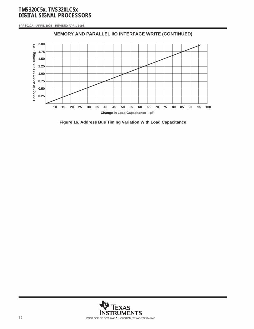
TMS320C5x, TMS320LC5xDIGITAL SIGNAL PROCESSORS
SPRS030A – APRIL 1995 – REVISED APRIL 1996
62 POST OFFICE BOX 1443 • HOUSTON, TEXAS 77251–1443
MEMORY AND PARALLEL I/O INTERFACE WRITE (CONTINUED)
2.00
1.00
0.75
0.50
0.25
1.25
1.50
1.75
10 30 55 70 8515 20 25 4535 40 50 8060 65 75 90 95 100
Cha
nge
in A
ddre
ss B
us T
imin
g–
ns
Change in Load Capacitance – pF
Figure 16. Address Bus Timing Variation With Load Capacitance
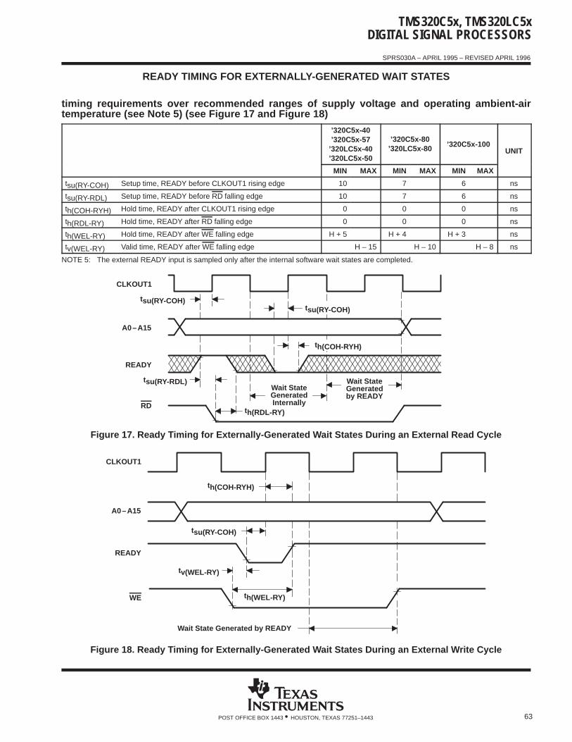
TMS320C5x, TMS320LC5xDIGITAL SIGNAL PROCESSORS
SPRS030A – APRIL 1995 – REVISED APRIL 1996
63POST OFFICE BOX 1443 • HOUSTON, TEXAS 77251–1443
READY TIMING FOR EXTERNALLY-GENERATED WAIT STATES
timing requirements over recommended ranges of supply voltage and operating ambient-airtemperature (see Note 5) (see Figure 17 and Figure 18)
’320C5x-40’320C5x-57
’320LC5x-40’320LC5x-50
’320C5x-80’320LC5x-80 ’320C5x-100
UNIT
MIN MAX MIN MAX MIN MAX
tsu(RY-COH) Setup time, READY before CLKOUT1 rising edge 10 7 6 ns
tsu(RY-RDL) Setup time, READY before RD falling edge 10 7 6 ns
th(COH-RYH) Hold time, READY after CLKOUT1 rising edge 0 0 0 ns
th(RDL-RY) Hold time, READY after RD falling edge 0 0 0 ns
th(WEL-RY) Hold time, READY after WE falling edge H + 5 H + 4 H + 3 ns
tv(WEL-RY) Valid time, READY after WE falling edge H – 15 H – 10 H – 8 ns
NOTE 5: The external READY input is sampled only after the internal software wait states are completed.
READY
A0–A15
CLKOUT1
RD
Wait StateGeneratedby READY
Wait StateGeneratedInternally
th(RDL-RY)
tsu(RY-COH)tsu(RY-COH)
th(COH-RYH)
tsu(RY-RDL)
Figure 17. Ready Timing for Externally-Generated Wait States During an External Read Cycle
READY
A0–A15
CLKOUT1
Wait State Generated by READY
WE
th(COH-RYH)
tsu(RY-COH)
th(WEL-RY)
tv(WEL-RY)
Figure 18. Ready Timing for Externally-Generated Wait States During an External Write Cycle
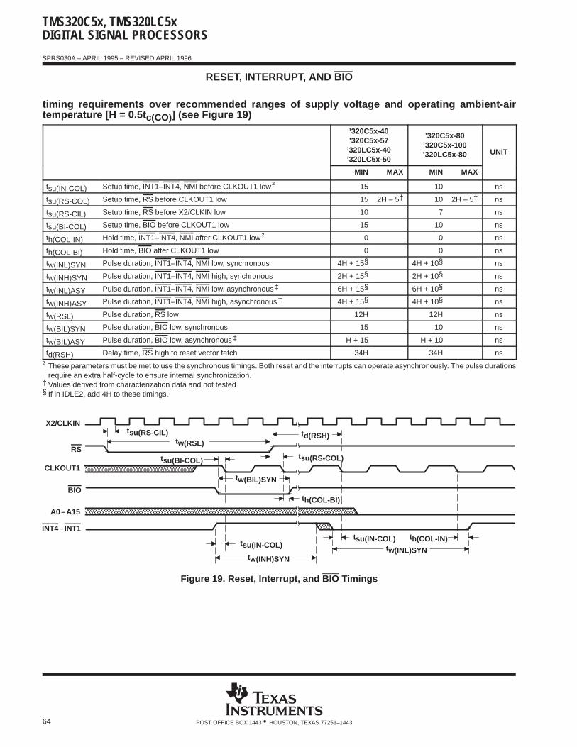
TMS320C5x, TMS320LC5xDIGITAL SIGNAL PROCESSORS
SPRS030A – APRIL 1995 – REVISED APRIL 1996
64 POST OFFICE BOX 1443 • HOUSTON, TEXAS 77251–1443
RESET, INTERRUPT, AND BIO
timing requirements over recommended ranges of supply voltage and operating ambient-airtemperature [H = 0.5t c(CO)] (see Figure 19)
’320C5x-40’320C5x-57
’320LC5x-40’320LC5x-50
’320C5x-80’320C5x-100’320LC5x-80 UNIT
MIN MAX MIN MAX
tsu(IN-COL) Setup time, INT1–INT4, NMI before CLKOUT1 low† 15 10 ns
tsu(RS-COL) Setup time, RS before CLKOUT1 low 15 2H – 5‡ 10 2H – 5‡ ns
tsu(RS-CIL) Setup time, RS before X2/CLKIN low 10 7 ns
tsu(BI-COL) Setup time, BIO before CLKOUT1 low 15 10 ns
th(COL-IN) Hold time, INT1–INT4, NMI after CLKOUT1 low† 0 0 ns
th(COL-BI) Hold time, BIO after CLKOUT1 low 0 0 ns
tw(INL)SYN Pulse duration, INT1–INT4, NMI low, synchronous 4H + 15§ 4H + 10§ ns
tw(INH)SYN Pulse duration, INT1–INT4, NMI high, synchronous 2H + 15§ 2H + 10§ ns
tw(INL)ASY Pulse duration, INT1–INT4, NMI low, asynchronous‡ 6H + 15§ 6H + 10§ ns
tw(INH)ASY Pulse duration, INT1–INT4, NMI high, asynchronous‡ 4H + 15§ 4H + 10§ ns
tw(RSL) Pulse duration, RS low 12H 12H ns
tw(BIL)SYN Pulse duration, BIO low, synchronous 15 10 ns
tw(BIL)ASY Pulse duration, BIO low, asynchronous‡ H + 15 H + 10 ns
td(RSH) Delay time, RS high to reset vector fetch 34H 34H ns
† These parameters must be met to use the synchronous timings. Both reset and the interrupts can operate asynchronously. The pulse durationsrequire an extra half-cycle to ensure internal synchronization.
‡ Values derived from characterization data and not tested§ If in IDLE2, add 4H to these timings.
BIO
RS
X2/CLKINtsu(RS-CIL)
tsu(BI-COL)
tsu(IN-COL)
th(COL-BI)
A0–A15
tsu(IN-COL)th(COL-IN)
tw(BIL)SYN
td(RSH)
CLKOUT1
tw(RSL)
INT4–INT1
tw(INH)SYNtw(INL)SYN
tsu(RS-COL)
Figure 19. Reset, Interrupt, and BIO Timings
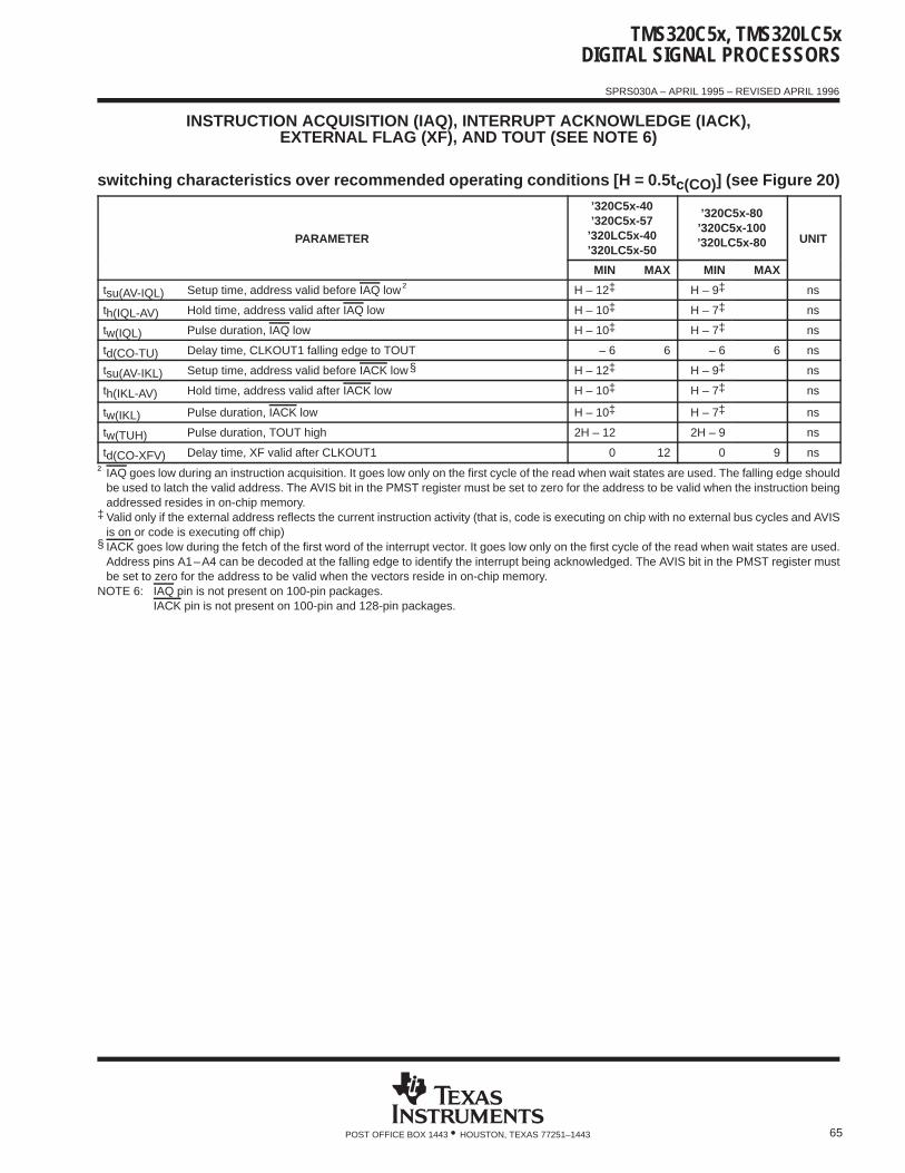
TMS320C5x, TMS320LC5xDIGITAL SIGNAL PROCESSORS
SPRS030A – APRIL 1995 – REVISED APRIL 1996
65POST OFFICE BOX 1443 • HOUSTON, TEXAS 77251–1443
INSTRUCTION ACQUISITION (IAQ), INTERRUPT ACKNOWLEDGE (IACK),EXTERNAL FLAG (XF), AND TOUT (SEE NOTE 6)
switching characteristics over recommended operating conditions [H = 0.5t c(CO)] (see Figure 20)
PARAMETER
’320C5x-40’320C5x-57
’320LC5x-40’320LC5x-50
’320C5x-80’320C5x-100’320LC5x-80 UNIT
MIN MAX MIN MAX
tsu(AV-IQL) Setup time, address valid before IAQ low† H – 12‡ H – 9‡ ns
th(IQL-AV) Hold time, address valid after IAQ low H – 10‡ H – 7‡ ns
tw(IQL) Pulse duration, IAQ low H – 10‡ H – 7‡ ns
td(CO-TU) Delay time, CLKOUT1 falling edge to TOUT – 6 6 – 6 6 ns
tsu(AV-IKL) Setup time, address valid before IACK low§ H – 12‡ H – 9‡ ns
th(IKL-AV) Hold time, address valid after IACK low H – 10‡ H – 7‡ ns
tw(IKL) Pulse duration, IACK low H – 10‡ H – 7‡ ns
tw(TUH) Pulse duration, TOUT high 2H – 12 2H – 9 ns
td(CO-XFV) Delay time, XF valid after CLKOUT1 0 12 0 9 ns
† IAQ goes low during an instruction acquisition. It goes low only on the first cycle of the read when wait states are used. The falling edge shouldbe used to latch the valid address. The AVIS bit in the PMST register must be set to zero for the address to be valid when the instruction beingaddressed resides in on-chip memory.
‡ Valid only if the external address reflects the current instruction activity (that is, code is executing on chip with no external bus cycles and AVISis on or code is executing off chip)
§ IACK goes low during the fetch of the first word of the interrupt vector. It goes low only on the first cycle of the read when wait states are used.Address pins A1–A4 can be decoded at the falling edge to identify the interrupt being acknowledged. The AVIS bit in the PMST register mustbe set to zero for the address to be valid when the vectors reside in on-chip memory.
NOTE 6: IAQ pin is not present on 100-pin packages. IACK pin is not present on 100-pin and 128-pin packages.
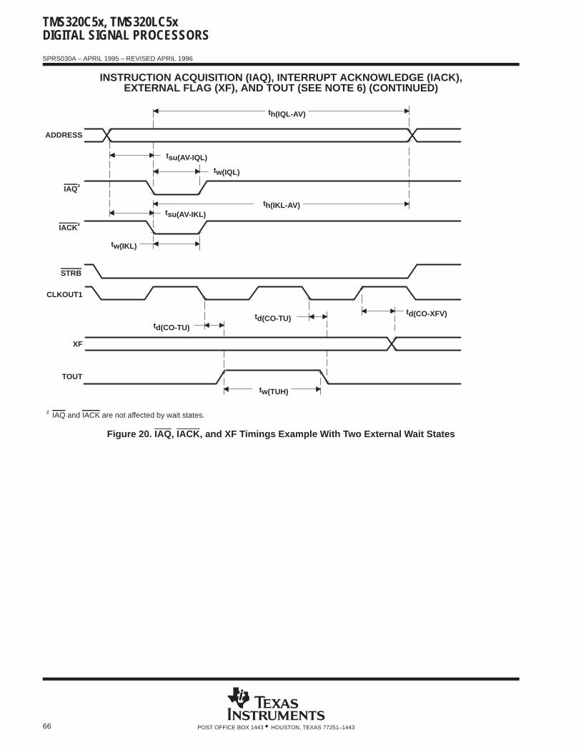
TMS320C5x, TMS320LC5xDIGITAL SIGNAL PROCESSORS
SPRS030A – APRIL 1995 – REVISED APRIL 1996
66 POST OFFICE BOX 1443 • HOUSTON, TEXAS 77251–1443
INSTRUCTION ACQUISITION (IAQ), INTERRUPT ACKNOWLEDGE (IACK),EXTERNAL FLAG (XF), AND TOUT (SEE NOTE 6) (CONTINUED)
CLKOUT1
STRB
IACK†
IAQ†
ADDRESS
td(CO-TU)
tw(IKL)
tsu(AV-IKL)
tsu(AV-IQL)
tw(IQL)
th(IKL-AV)
th(IQL-AV)
XF
TOUT
td(CO-XFV)
tw(TUH)
td(CO-TU)
† IAQ and IACK are not affected by wait states.
Figure 20. IAQ , IACK, and XF Timings Example With Two External Wait States
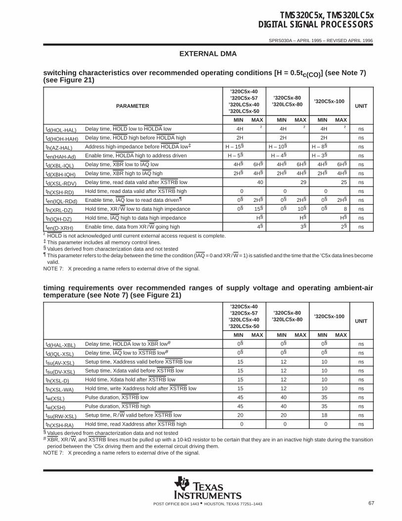
TMS320C5x, TMS320LC5xDIGITAL SIGNAL PROCESSORS
SPRS030A – APRIL 1995 – REVISED APRIL 1996
67POST OFFICE BOX 1443 • HOUSTON, TEXAS 77251–1443
EXTERNAL DMA
switching characteristics over recommended operating conditions [H = 0.5t c(CO)] (see Note 7)(see Figure 21)
PARAMETER
’320C5x-40’320C5x-57
’320LC5x-40’320LC5x-50
’320C5x-80’320LC5x-80 ’320C5x-100
UNIT
MIN MAX MIN MAX MIN MAX
td(HOL-HAL) Delay time, HOLD low to HOLDA low 4H † 4H † 4H † ns
td(HOH-HAH) Delay time, HOLD high before HOLDA high 2H 2H 2H ns
th(AZ-HAL) Address high-impedance before HOLDA low‡ H – 15§ H – 10§ H – 8§ ns
ten(HAH-Ad) Enable time, HOLDA high to address driven H – 5§ H – 4§ H – 3§ ns
td(XBL-IQL) Delay time, XBR low to IAQ low 4H§ 6H§ 4H§ 6H§ 4H§ 6H§ ns
td(XBH-IQH) Delay time, XBR high to IAQ high 2H§ 4H§ 2H§ 4H§ 2H§ 4H§ ns
td(XSL-RDV) Delay time, read data valid after XSTRB low 40 29 25 ns
th(XSH-RD) Hold time, read data valid after XSTRB high 0 0 0 ns
ten(IQL-RDd) Enable time, IAQ low to read data driven¶ 0§ 2H§ 0§ 2H§ 0§ 2H§ ns
th(XRL-DZ) Hold time, XR/W low to data high impedance 0§ 15§ 0§ 10§ 0§ 8 ns
th(IQH-DZ) Hold time, IAQ high to data high impedance H§ H§ H§ ns
ten(D-XRH) Enable time, data from XR/W going high 4§ 3§ 2§ ns
† HOLD is not acknowledged until current external access request is complete.‡ This parameter includes all memory control lines.§ Values derived from characterization data and not tested¶ This parameter refers to the delay between the time the condition (IAQ = 0 and XR/W = 1) is satisfied and the time that the ’C5x data lines become
valid.NOTE 7: X preceding a name refers to external drive of the signal.
timing requirements over recommended ranges of supply voltage and operating ambient-airtemperature (see Note 7) (see Figure 21)
’320C5x-40’320C5x-57
’320LC5x-40’320LC5x-50
’320C5x-80’320LC5x-80 ’320C5x-100
UNIT
MIN MAX MIN MAX MIN MAX
td(HAL-XBL) Delay time, HOLDA low to XBR low# 0§ 0§ 0§ ns
td(IQL-XSL) Delay time, IAQ low to XSTRB low# 0§ 0§ 0§ ns
tsu(AV-XSL) Setup time, Xaddress valid before XSTRB low 15 12 10 ns
tsu(DV-XSL) Setup time, Xdata valid before XSTRB low 15 12 10 ns
th(XSL-D) Hold time, Xdata hold after XSTRB low 15 12 10 ns
th(XSL-WA) Hold time, write Xaddress hold after XSTRB low 15 12 10 ns
tw(XSL) Pulse duration, XSTRB low 45 40 35 ns
tw(XSH) Pulse duration, XSTRB high 45 40 35 ns
tsu(RW-XSL) Setup time, R /W valid before XSTRB low 20 20 18 ns
th(XSH-RA) Hold time, read Xaddress after XSTRB high 0 0 0 ns
§ Values derived from characterization data and not tested# XBR, XR/W, and XSTRB lines must be pulled up with a 10-kΩ resistor to be certain that they are in an inactive high state during the transition
period between the ’C5x driving them and the external circuit driving them.NOTE 7: X preceding a name refers to external drive of the signal.
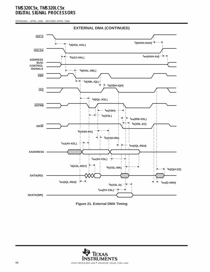
TMS320C5x, TMS320LC5xDIGITAL SIGNAL PROCESSORS
SPRS030A – APRIL 1995 – REVISED APRIL 1996
68 POST OFFICE BOX 1443 • HOUSTON, TEXAS 77251–1443
EXTERNAL DMA (CONTINUED)
XDATA(WR)
DATA(RD)
XADDRESS
XR/W
XSTRB
IAQ
XBR
ADDRESSBUS/
CONTROLSIGNALS
HOLDA
HOLD
tsu(DV-XSL)
th(XRL-DZ)
td(IQL-XSL)
td(XBL-IQL)
td(HAL-XBL)
ten(HAH-Ad)th(AZ-HAL)
td(HOH-HAH)td(HOL-HAL)
tsu(AV-XSL)
tw(XSH)
tsu(RW-XSL)tw(XSL)
td(XBH-IQH)
ten(IQL-RDd) ten(D-XRH)
th(IQH-DZ)
ten(IQL-RDd)
tsu(AV-XSL)
th(XSL-WA)
th(XSL-D)
th(XSH-RA)
td(XSL-RDV)
th(XSH-RD)
Figure 21. External DMA Timing
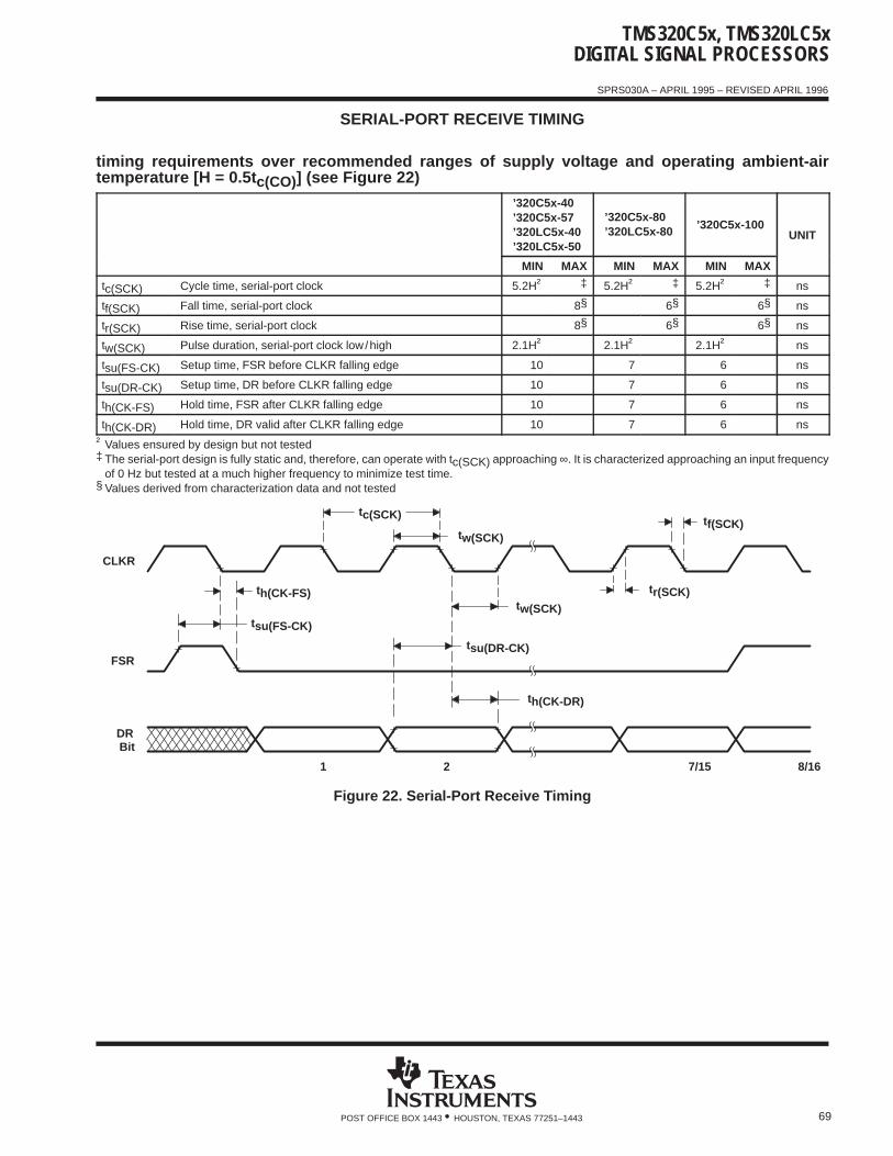
TMS320C5x, TMS320LC5xDIGITAL SIGNAL PROCESSORS
SPRS030A – APRIL 1995 – REVISED APRIL 1996
69POST OFFICE BOX 1443 • HOUSTON, TEXAS 77251–1443
SERIAL-PORT RECEIVE TIMING
timing requirements over recommended ranges of supply voltage and operating ambient-airtemperature [H = 0.5t c(CO)] (see Figure 22)
’320C5x-40’320C5x-57’320LC5x-40’320LC5x-50
’320C5x-80’320LC5x-80 ’320C5x-100
UNIT
MIN MAX MIN MAX MIN MAX
tc(SCK) Cycle time, serial-port clock 5.2H† ‡ 5.2H† ‡ 5.2H† ‡ ns
tf(SCK) Fall time, serial-port clock 8§ 6§ 6§ ns
tr(SCK) Rise time, serial-port clock 8§ 6§ 6§ ns
tw(SCK) Pulse duration, serial-port clock low/high 2.1H† 2.1H† 2.1H† ns
tsu(FS-CK) Setup time, FSR before CLKR falling edge 10 7 6 ns
tsu(DR-CK) Setup time, DR before CLKR falling edge 10 7 6 ns
th(CK-FS) Hold time, FSR after CLKR falling edge 10 7 6 ns
th(CK-DR) Hold time, DR valid after CLKR falling edge 10 7 6 ns
† Values ensured by design but not tested‡ The serial-port design is fully static and, therefore, can operate with tc(SCK) approaching ∞. It is characterized approaching an input frequency
of 0 Hz but tested at a much higher frequency to minimize test time.§ Values derived from characterization data and not tested
BitDR
FSR
CLKR
8/167/1521
tsu(DR-CK)
tsu(FS-CK)
th(CK-FS)tw(SCK)
tr(SCK)
tf(SCK)tw(SCK)
th(CK-DR)
tc(SCK)
Figure 22. Serial-Port Receive Timing
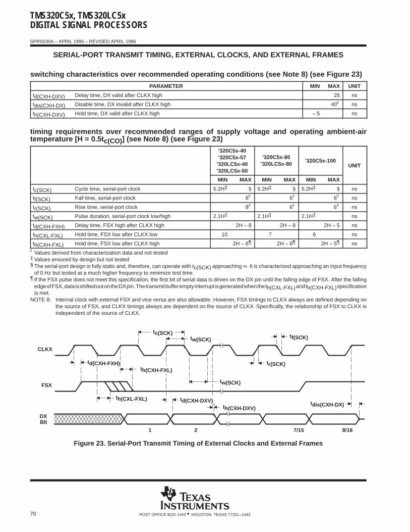
TMS320C5x, TMS320LC5xDIGITAL SIGNAL PROCESSORS
SPRS030A – APRIL 1995 – REVISED APRIL 1996
70 POST OFFICE BOX 1443 • HOUSTON, TEXAS 77251–1443
SERIAL-PORT TRANSMIT TIMING, EXTERNAL CLOCKS, AND EXTERNAL FRAMES
switching characteristics over recommended operating conditions (see Note 8) (see Figure 23)
PARAMETER MIN MAX UNIT
td(CXH-DXV) Delay time, DX valid after CLKX high 25 ns
tdis(CXH-DX) Disable time, DX invalid after CLKX high 40† ns
th(CXH-DXV) Hold time, DX valid after CLKX high – 5 ns
timing requirements over recommended ranges of supply voltage and operating ambient-airtemperature [H = 0.5t c(CO)] (see Note 8) (see Figure 23)
’320C5x-40’320C5x-57
’320LC5x-40’320LC5x-50
’320C5x-80’320LC5x-80 ’320C5x-100
UNIT
MIN MAX MIN MAX MIN MAX
tc(SCK) Cycle time, serial-port clock 5.2H‡ § 5.2H‡ § 5.2H‡ § ns
tf(SCK) Fall time, serial-port clock 8† 6† 6† ns
tr(SCK) Rise time, serial-port clock 8† 6† 6† ns
tw(SCK) Pulse duration, serial-port clock low/high 2.1H‡ 2.1H‡ 2.1H‡ ns
td(CXH-FXH) Delay time, FSX high after CLKX high 2H – 8 2H – 8 2H – 5 ns
th(CXL-FXL) Hold time, FSX low after CLKX low 10 7 6 ns
th(CXH-FXL) Hold time, FSX low after CLKX high 2H – 8¶ 2H – 8¶ 2H – 5¶ ns
† Values derived from characterization data and not tested‡ Values ensured by design but not tested§ The serial-port design is fully static and, therefore, can operate with tc(SCK) approaching ∞. It is characterized approaching an input frequency
of 0 Hz but tested at a much higher frequency to minimize test time.¶ If the FSX pulse does not meet this specification, the first bit of serial data is driven on the DX pin until the falling edge of FSX. After the falling
edge of FSX, data is shifted out on the DX pin. The transmit buffer empty interrupt is generated when the th(CXL-FXL) and th(CXH-FXL) specificationis met.
NOTE 8: Internal clock with external FSX and vice versa are also allowable. However, FSX timings to CLKX always are defined depending onthe source of FSX, and CLKX timings always are dependent on the source of CLKX. Specifically, the relationship of FSX to CLKX isindependent of the source of CLKX.
td(CXH-FXH)
DXBIt
FSX
CLKX
8/167/1521
th(CXH-DXV)
tw(SCK)
tr(SCK)
tf(SCK)tw(SCK)tc(SCK)
tdis(CXH-DX)th(CXL-FXL) td(CXH-DXV)
th(CXH-FXL)
Figure 23. Serial-Port Transmit Timing of External Clocks and External Frames
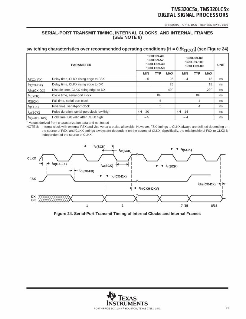
TMS320C5x, TMS320LC5xDIGITAL SIGNAL PROCESSORS
SPRS030A – APRIL 1995 – REVISED APRIL 1996
71POST OFFICE BOX 1443 • HOUSTON, TEXAS 77251–1443
SERIAL-PORT TRANSMIT TIMING, INTERNAL CLOCKS, AND INTERNAL FRAMES(SEE NOTE 8)
switching characteristics over recommended operating conditions [H = 0.5t c(CO)] (see Figure 24)
PARAMETER
’320C5x-40’320C5x-57
’320LC5x-40’320LC5x-50
’320C5x-80’320C5x-100’320LC5x-80 UNIT
MIN TYP MAX MIN TYP MAX
td(CX-FX) Delay time, CLKX rising edge to FSX – 5 25 – 4 18 ns
td(CX-DX) Delay time, CLKX rising edge to DX 25 18 ns
tdis(CX-DX) Disable time, CLKX rising edge to DX 40† 29† ns
tc(SCK) Cycle time, serial-port clock 8H 8H ns
tf(SCK) Fall time, serial-port clock 5 4 ns
tr(SCK) Rise time, serial-port clock 5 4 ns
tw(SCK) Pulse duration, serial-port clock low/high 4H – 20 4H – 14 ns
th(CXH-DXV) Hold time, DX valid after CLKX high – 5 – 4 ns
† Values derived from characterization data and not testedNOTE 8: Internal clock with external FSX and vice versa are also allowable. However, FSX timings to CLKX always are defined depending on
the source of FSX, and CLKX timings always are dependent on the source of CLKX. Specifically, the relationship of FSX to CLKX isindependent of the source of CLKX.
DXBit
FSX
CLKX
21
th(CXH-DXV)
tr(SCK)
tf(SCK)tw(SCK)
tc(SCK)
td(CX-FX)
td(CX-FX)td(CX-DX)
tdis(CX-DX)
tw(SCK)
8/167 /15
Figure 24. Serial-Port Transmit Timing of Internal Clocks and Internal Frames
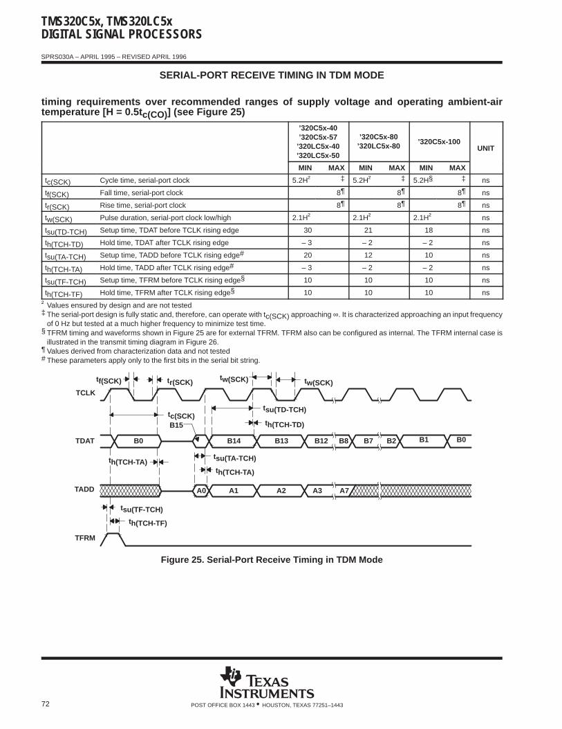
TMS320C5x, TMS320LC5xDIGITAL SIGNAL PROCESSORS
SPRS030A – APRIL 1995 – REVISED APRIL 1996
72 POST OFFICE BOX 1443 • HOUSTON, TEXAS 77251–1443
SERIAL-PORT RECEIVE TIMING IN TDM MODE
timing requirements over recommended ranges of supply voltage and operating ambient-airtemperature [H = 0.5t c(CO)] (see Figure 25)
’320C5x-40’320C5x-57
’320LC5x-40’320LC5x-50
’320C5x-80’320LC5x-80 ’320C5x-100
UNIT
MIN MAX MIN MAX MIN MAX
tc(SCK) Cycle time, serial-port clock 5.2H† ‡ 5.2H† ‡ 5.2H§ ‡ ns
tf(SCK) Fall time, serial-port clock 8¶ 8¶ 8¶ ns
tr(SCK) Rise time, serial-port clock 8¶ 8¶ 8¶ ns
tw(SCK) Pulse duration, serial-port clock low/high 2.1H† 2.1H† 2.1H† ns
tsu(TD-TCH) Setup time, TDAT before TCLK rising edge 30 21 18 ns
th(TCH-TD) Hold time, TDAT after TCLK rising edge – 3 – 2 – 2 ns
tsu(TA-TCH) Setup time, TADD before TCLK rising edge# 20 12 10 ns
th(TCH-TA) Hold time, TADD after TCLK rising edge# – 3 – 2 – 2 ns
tsu(TF-TCH) Setup time, TFRM before TCLK rising edge§ 10 10 10 ns
th(TCH-TF) Hold time, TFRM after TCLK rising edge§ 10 10 10 ns
† Values ensured by design and are not tested‡ The serial-port design is fully static and, therefore, can operate with tc(SCK) approaching ∞. It is characterized approaching an input frequency
of 0 Hz but tested at a much higher frequency to minimize test time.§ TFRM timing and waveforms shown in Figure 25 are for external TFRM. TFRM also can be configured as internal. The TFRM internal case is
illustrated in the transmit timing diagram in Figure 26.¶ Values derived from characterization data and not tested# These parameters apply only to the first bits in the serial bit string.
A7
B2B8 B7
A3
B12
A2A0 A1
B0B1B13B14
B15
B0
tw(SCK)tw(SCK)
tsu(TD-TCH)
th(TCH-TD)
tsu(TA-TCH)
th(TCH-TA)
tr(SCK)tf(SCK)
tc(SCK)
TFRM
TADD
TDAT
TCLK
th(TCH-TF)
tsu(TF-TCH)
th(TCH-TA)
Figure 25. Serial-Port Receive Timing in TDM Mode
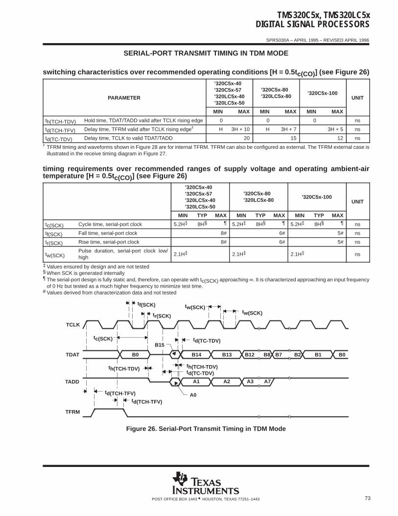
TMS320C5x, TMS320LC5xDIGITAL SIGNAL PROCESSORS
SPRS030A – APRIL 1995 – REVISED APRIL 1996
73POST OFFICE BOX 1443 • HOUSTON, TEXAS 77251–1443
SERIAL-PORT TRANSMIT TIMING IN TDM MODE
switching characteristics over recommended operating conditions [H = 0.5t c(CO)] (see Figure 26)
PARAMETER
’320C5x-40’320C5x-57’320LC5x-40’320LC5x-50
’320C5x-80’320LC5x-80 ’320C5x-100
UNIT
MIN MAX MIN MAX MIN MAX
th(TCH-TDV) Hold time, TDAT/TADD valid after TCLK rising edge 0 0 0 ns
td(TCH-TFV) Delay time, TFRM valid after TCLK rising edge† H 3H + 10 H 3H + 7 3H + 5 ns
td(TC-TDV) Delay time, TCLK to valid TDAT/TADD 20 15 12 ns
† TFRM timing and waveforms shown in Figure 28 are for internal TFRM. TFRM can also be configured as external. The TFRM external case isillustrated in the receive timing diagram in Figure 27.
timing requirements over recommended ranges of supply voltage and operating ambient-airtemperature [H = 0.5t c(CO)] (see Figure 26)
’320C5x-40’320C5x-57’320LC5x-40’320LC5x-50
’320C5x-80’320LC5x-80 ’320C5x-100
UNIT
MIN TYP MAX MIN TYP MAX MIN TYP MAX
tc(SCK) Cycle time, serial-port clock 5.2H‡ 8H§ ¶ 5.2H‡ 8H§ ¶ 5.2H‡ 8H§ ¶ ns
tf(SCK) Fall time, serial-port clock 8# 6# 5# ns
tr(SCK) Rise time, serial-port clock 8# 6# 5# ns
tw(SCK)Pulse duration, serial-port clock low/high
2.1H‡ 2.1H‡ 2.1H‡ ns
‡ Values ensured by design and are not tested§ When SCK is generated internally¶ The serial-port design is fully static and, therefore, can operate with tc(SCK) approaching ∞. It is characterized approaching an input frequency
of 0 Hz but tested as a much higher frequency to minimize test time.# Values derived from characterization data and not tested
A7
B2B8 B7
A3
B12
A2
A0
A1
B0B1B13B14B0
tw(SCK)tw(SCK)
td(TC-TDV)th(TCH-TDV)
tr(SCK)
tf(SCK)
td(TCH-TFV)
TFRM
TADD
TDAT
TCLK
B15tc(SCK) td(TC-TDV)
th(TCH-TDV)
td(TCH-TFV)
Figure 26. Serial-Port Transmit Timing in TDM Mode
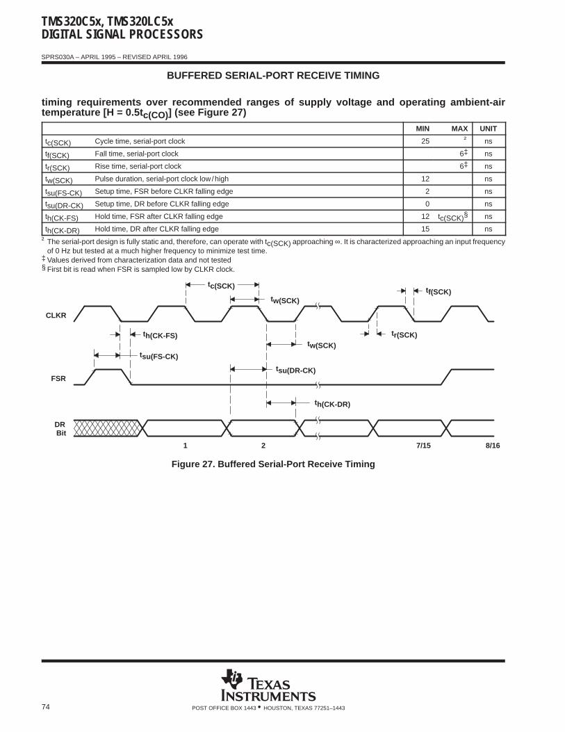
TMS320C5x, TMS320LC5xDIGITAL SIGNAL PROCESSORS
SPRS030A – APRIL 1995 – REVISED APRIL 1996
74 POST OFFICE BOX 1443 • HOUSTON, TEXAS 77251–1443
BUFFERED SERIAL-PORT RECEIVE TIMING
timing requirements over recommended ranges of supply voltage and operating ambient-airtemperature [H = 0.5t c(CO)] (see Figure 27)
MIN MAX UNIT
tc(SCK) Cycle time, serial-port clock 25 † ns
tf(SCK) Fall time, serial-port clock 6‡ ns
tr(SCK) Rise time, serial-port clock 6‡ ns
tw(SCK) Pulse duration, serial-port clock low/high 12 ns
tsu(FS-CK) Setup time, FSR before CLKR falling edge 2 ns
tsu(DR-CK) Setup time, DR before CLKR falling edge 0 ns
th(CK-FS) Hold time, FSR after CLKR falling edge 12 tc(SCK)§ ns
th(CK-DR) Hold time, DR after CLKR falling edge 15 ns
† The serial-port design is fully static and, therefore, can operate with tc(SCK) approaching ∞. It is characterized approaching an input frequencyof 0 Hz but tested at a much higher frequency to minimize test time.
‡ Values derived from characterization data and not tested§ First bit is read when FSR is sampled low by CLKR clock.
BitDR
FSR
CLKR
8/167/1521
tsu(DR-CK)
tsu(FS-CK)
th(CK-FS)tw(SCK)
tr(SCK)
tf(SCK)tw(SCK)
th(CK-DR)
tc(SCK)
Figure 27. Buffered Serial-Port Receive Timing

TMS320C5x, TMS320LC5xDIGITAL SIGNAL PROCESSORS
SPRS030A – APRIL 1995 – REVISED APRIL 1996
75POST OFFICE BOX 1443 • HOUSTON, TEXAS 77251–1443
BUFFERED SERIAL-PORT TRANSMIT TIMING OF EXTERNAL FRAMES (SEE NOTES 9 AND 10)
switching characteristics over recommended operating conditions (see Figure 28)
PARAMETER MIN MAX UNIT
td(CXH-DXV) Delay time, DX valid after CLKX rising edge 5 21 ns
tdis(CXH-DX) Disable time, DX invalid after CLKX rising edge 5 15 ns
tdis(CXH-DX)PCM Disable time in PCM mode, DX invalid after CLKX rising edge 15 ns
ten(CXH-DX)PCM Enable time in PCM mode, DX valid after CLKX rising edge 21 ns
th(CXH-DXV) Hold time, DX valid after CLKX rising edge 5 20 ns
timing requirements over recommended operating conditions (see Figure 28)
MIN MAX UNIT
tc(SCK) Cycle time, serial-port clock 25 † ns
tf(SCK) Fall time, serial-port clock 4‡ ns
tr(SCK) Rise time, serial-port clock 4‡ ns
tw(SCK) Pulse duration, serial-port clock low/high 8.5 ns
tsu(FX-CXL) Setup time, FSX before CLKX falling edge 5 ns
th(CXL-FX) Hold time, FSX after CLKX falling edge 5 tc(SCK)–5§ ns
† The serial-port design is fully static and, therefore, can operate with tc(SCK) approaching ∞. It is characterized approaching an input frequencyof 0 Hz but tested at a much higher frequency to minimize test time.
‡ Values derived from characterization data and not tested§ If the FSX pulse does not meet this specification, the first bit of the serial data is driven on the DX pin until FSX goes low (sampled on falling edge
of CLKX). After falling edge of the FSX, data is shifted out on the DX pin.NOTE 9: Internal clock with external FSX and vice versa are also allowable. However, FSX timings to CLKX always are defined depending on
the source of FSX, and CLKX timings always are dependent upon the source of CLKX. Specifically, the relationship of FSX to CLKXis independent of the source of CLKX. External FSX timings are obtained from the “timing requirements over recommended operatingconditions” table listed in the “Buffered Serial-Port Transmit Timing of External Frames” section and internal FSX timings are obtainedfrom the “switching characteristics over recommended operating conditions” table listed under the “Buffered Serial-Port Transmit Timingof Internal Frame and Internal Clock” section. Internal CLKX timings are obtained from the “switching characteristics over recommendedoperating conditions” table listed under the “Buffered Serial-Port Transmit Timing of Internal Frame and Internal Clock” section andexternal CLKX timings are obtained from the “timing requirements over recommended operating conditions” table in the “BufferedSerial-Port Transmit Timing of External Frames” section.
NOTE 10: Timings for CLKX and FSX are given with polarity bits (CLKP and FSP) set to 0
DX BIt
FSX
CLKX
8/167/1521
th(CXH-DXV)td(CXH-DXV)
tw(SCK)
tr(SCK)
tf(SCK)tw(SCK)tc(SCK)
th(CXL-FX)
tdis(CXH-DX)
tsu(FX-CXL)
Figure 28. Buffered Serial-Port Transmit Timing of External Clocks and External Frames
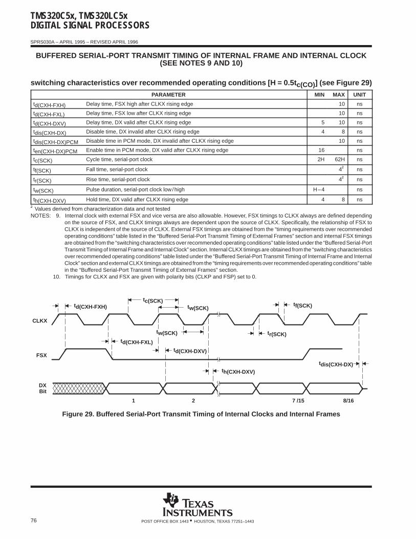
TMS320C5x, TMS320LC5xDIGITAL SIGNAL PROCESSORS
SPRS030A – APRIL 1995 – REVISED APRIL 1996
76 POST OFFICE BOX 1443 • HOUSTON, TEXAS 77251–1443
BUFFERED SERIAL-PORT TRANSMIT TIMING OF INTERNAL FRAME AND INTERNAL CLOCK(SEE NOTES 9 AND 10)
switching characteristics over recommended operating conditions [H = 0.5t c(CO)] (see Figure 29)
PARAMETER MIN MAX UNIT
td(CXH-FXH) Delay time, FSX high after CLKX rising edge 10 ns
td(CXH-FXL) Delay time, FSX low after CLKX rising edge 10 ns
td(CXH-DXV) Delay time, DX valid after CLKX rising edge 5 10 ns
tdis(CXH-DX) Disable time, DX invalid after CLKX rising edge 4 8 ns
tdis(CXH-DX)PCM Disable time in PCM mode, DX invalid after CLKX rising edge 10 ns
ten(CXH-DX)PCM Enable time in PCM mode, DX valid after CLKX rising edge 16 ns
tc(SCK) Cycle time, serial-port clock 2H 62H ns
tf(SCK) Fall time, serial-port clock 4† ns
tr(SCK) Rise time, serial-port clock 4† ns
tw(SCK) Pulse duration, serial-port clock low/high H–4 ns
th(CXH-DXV) Hold time, DX valid after CLKX rising edge 4 8 ns
† Values derived from characterization data and not testedNOTES: 9. Internal clock with external FSX and vice versa are also allowable. However, FSX timings to CLKX always are defined depending
on the source of FSX, and CLKX timings always are dependent upon the source of CLKX. Specifically, the relationship of FSX toCLKX is independent of the source of CLKX. External FSX timings are obtained from the “timing requirements over recommendedoperating conditions” table listed in the “Buffered Serial-Port Transmit Timing of External Frames” section and internal FSX timingsare obtained from the “switching characteristics over recommended operating conditions” table listed under the “Buffered Serial-PortTransmit Timing of Internal Frame and Internal Clock” section. Internal CLKX timings are obtained from the “switching characteristicsover recommended operating conditions” table listed under the “Buffered Serial-Port Transmit Timing of Internal Frame and InternalClock” section and external CLKX timings are obtained from the “timing requirements over recommended operating conditions” tablein the “Buffered Serial-Port Transmit Timing of External Frames” section.
10. Timings for CLKX and FSX are given with polarity bits (CLKP and FSP) set to 0.
DXBit
FSX
CLKX
21
th(CXH-DXV)
tr(SCK)
tf(SCK)tw(SCK)
tc(SCK)
td(CXH-FXL)td(CXH-DXV)
tdis(CXH-DX)
tw(SCK)
8/167 /15
td(CXH-FXH)
Figure 29. Buffered Serial-Port Transmit Timing of Internal Clocks and Internal Frames
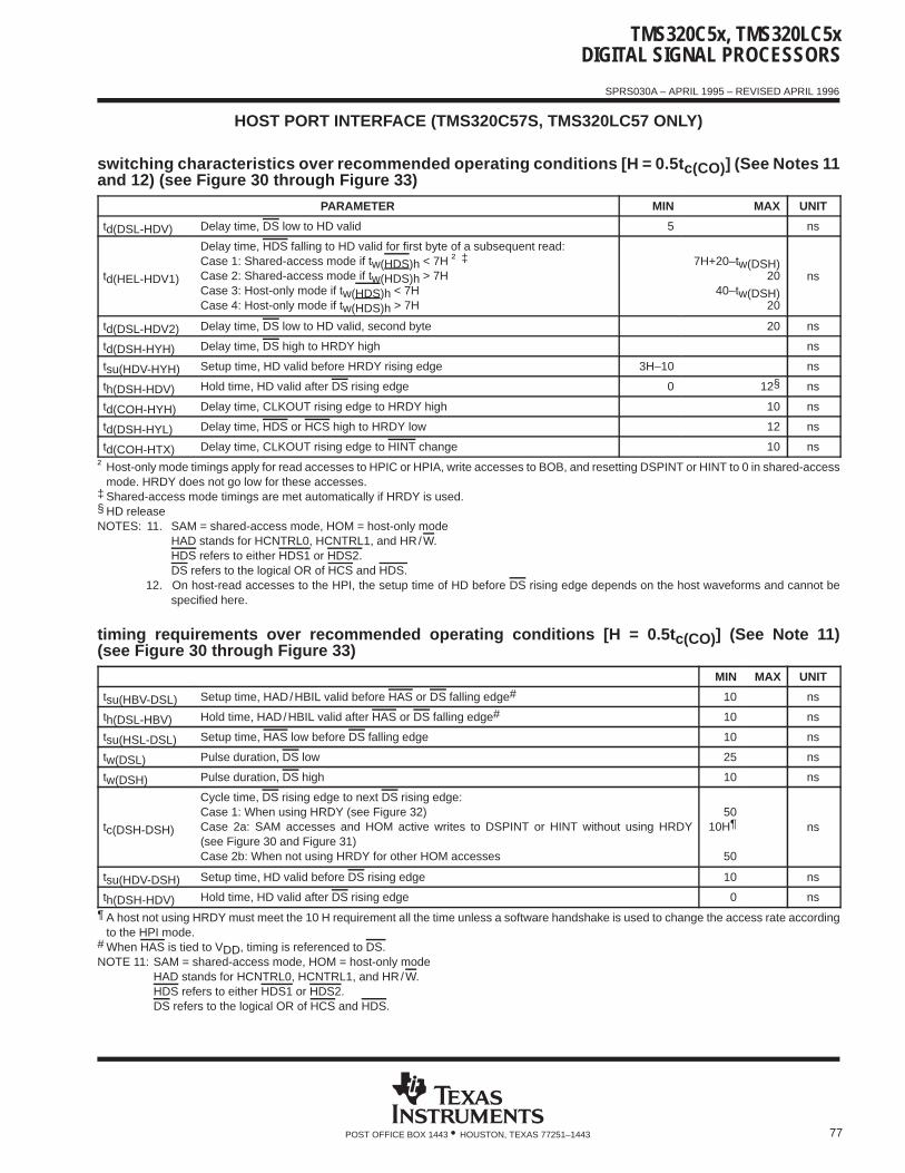
TMS320C5x, TMS320LC5xDIGITAL SIGNAL PROCESSORS
SPRS030A – APRIL 1995 – REVISED APRIL 1996
77POST OFFICE BOX 1443 • HOUSTON, TEXAS 77251–1443
HOST PORT INTERFACE (TMS320C57S, TMS320LC57 ONLY)
switching characteristics over recommended operating conditions [H = 0.5t c(CO)] (See Notes 11and 12) (see Figure 30 through Figure 33)
PARAMETER MIN MAX UNIT
td(DSL-HDV) Delay time, DS low to HD valid 5 ns
td(HEL-HDV1)
Delay time, HDS falling to HD valid for first byte of a subsequent read:Case 1: Shared-access mode if tw(HDS)h < 7H † ‡ Case 2: Shared-access mode if tw(HDS)h > 7HCase 3: Host-only mode if tw(HDS)h < 7HCase 4: Host-only mode if tw(HDS)h > 7H
7H+20–tw(DSH)20
40–tw(DSH)20
ns
td(DSL-HDV2) Delay time, DS low to HD valid, second byte 20 ns
td(DSH-HYH) Delay time, DS high to HRDY high ns
tsu(HDV-HYH) Setup time, HD valid before HRDY rising edge 3H–10 ns
th(DSH-HDV) Hold time, HD valid after DS rising edge 0 12§ ns
td(COH-HYH) Delay time, CLKOUT rising edge to HRDY high 10 ns
td(DSH-HYL) Delay time, HDS or HCS high to HRDY low 12 ns
td(COH-HTX) Delay time, CLKOUT rising edge to HINT change 10 ns
† Host-only mode timings apply for read accesses to HPIC or HPIA, write accesses to BOB, and resetting DSPINT or HINT to 0 in shared-accessmode. HRDY does not go low for these accesses.
‡ Shared-access mode timings are met automatically if HRDY is used.§ HD releaseNOTES: 11. SAM = shared-access mode, HOM = host-only mode
HAD stands for HCNTRL0, HCNTRL1, and HR/W.HDS refers to either HDS1 or HDS2.DS refers to the logical OR of HCS and HDS.
12. On host-read accesses to the HPI, the setup time of HD before DS rising edge depends on the host waveforms and cannot bespecified here.
timing requirements over recommended operating conditions [H = 0.5t c(CO)] (See Note 11)(see Figure 30 through Figure 33)
MIN MAX UNIT
tsu(HBV-DSL) Setup time, HAD/HBIL valid before HAS or DS falling edge# 10 ns
th(DSL-HBV) Hold time, HAD/HBIL valid after HAS or DS falling edge# 10 ns
tsu(HSL-DSL) Setup time, HAS low before DS falling edge 10 ns
tw(DSL) Pulse duration, DS low 25 ns
tw(DSH) Pulse duration, DS high 10 ns
tc(DSH-DSH)
Cycle time, DS rising edge to next DS rising edge:Case 1: When using HRDY (see Figure 32)Case 2a: SAM accesses and HOM active writes to DSPINT or HINT without using HRDY(see Figure 30 and Figure 31)Case 2b: When not using HRDY for other HOM accesses
5010H¶
50
ns
tsu(HDV-DSH) Setup time, HD valid before DS rising edge 10 ns
th(DSH-HDV) Hold time, HD valid after DS rising edge 0 ns
¶ A host not using HRDY must meet the 10 H requirement all the time unless a software handshake is used to change the access rate accordingto the HPI mode.
# When HAS is tied to VDD, timing is referenced to DS.NOTE 11: SAM = shared-access mode, HOM = host-only mode
HAD stands for HCNTRL0, HCNTRL1, and HR/W.HDS refers to either HDS1 or HDS2. DS refers to the logical OR of HCS and HDS.
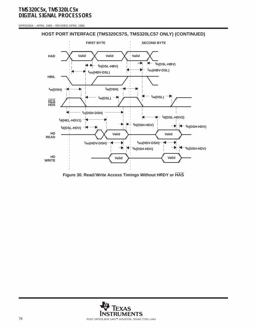
TMS320C5x, TMS320LC5xDIGITAL SIGNAL PROCESSORS
SPRS030A – APRIL 1995 – REVISED APRIL 1996
78 POST OFFICE BOX 1443 • HOUSTON, TEXAS 77251–1443
HOST PORT INTERFACE (TMS320C57S, TMS320LC57 ONLY) (CONTINUED)
HBIL
HAD
th(DSL-HBV)tsu(HBV-DSL)
th(DSL-HBV)
FIRST BYTE SECOND BYTE
HCSHDS
tw(DSL)
tc(DSH-DSH)
HDREAD
th(DSH-HDV) th(DSH-HDV)
HDWRITE
th(DSH-HDV)
tsu(HDV-DSH)
tsu(HBV-DSL)
td(DSL-HDV2)
tw(DSH) tw(DSH)
tw(DSL)
th(DSH-HDV)
tsu(HDV-DSH)
Valid Valid Valid
Valid Valid
ValidValid
td(HEL-HDV1)
td(DSL-HDV)
Figure 30. Read/Write Access Timings Without HRDY or HAS

TMS320C5x, TMS320LC5xDIGITAL SIGNAL PROCESSORS
SPRS030A – APRIL 1995 – REVISED APRIL 1996
79POST OFFICE BOX 1443 • HOUSTON, TEXAS 77251–1443
HOST PORT INTERFACE (TMS320C57S, TMS320LC57 ONLY) (CONTINUED)
FIRST BYTE SECOND BYTE
HAD
tsu(HSL-DSL)
th(DSL-HBV)
HBIL
tc(DSH-DSH)HCSHDS
HAS
tw(DSL)
tc(DSH-DSH)
HDREAD
th(DSH-HDV)th(DSH-HDV)
HDWRITE
th(DSH-HDV)
Valid Valid
ValidValid
td(DSL-HDV2)
tsu(HDV-DSH)tsu(HDV-DSH)
tw(DSH)
td(DSL-HDV)
td(HEL-HDV1)
th(DSH-HDV)
tsu(HBV-DSL)
Valid Valid Valid
Figure 31. Read/Write Access Timings Using HAS Without HRDY
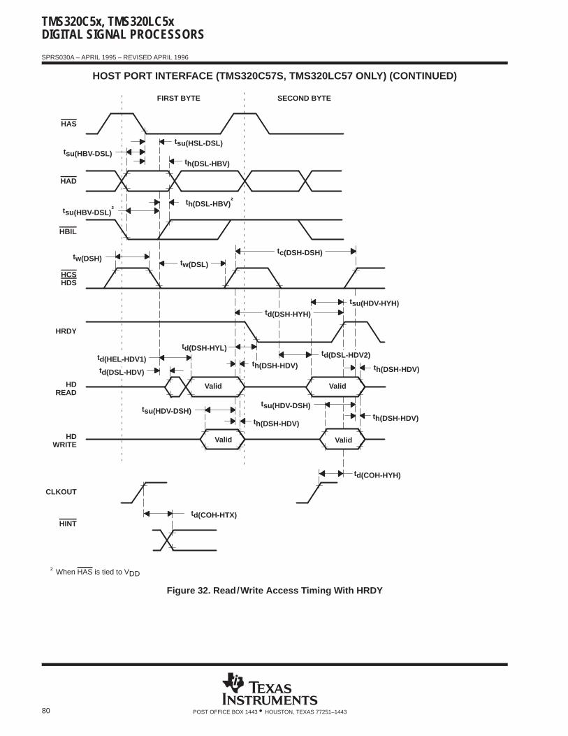
TMS320C5x, TMS320LC5xDIGITAL SIGNAL PROCESSORS
SPRS030A – APRIL 1995 – REVISED APRIL 1996
80 POST OFFICE BOX 1443 • HOUSTON, TEXAS 77251–1443
HOST PORT INTERFACE (TMS320C57S, TMS320LC57 ONLY) (CONTINUED)
FIRST BYTE SECOND BYTE
th(DSL-HBV) †
HRDY
td(DSH-HYL)
CLKOUT
td(COH-HYH)
HINTtd(COH-HTX)
† When HAS is tied to VDD
tsu(HBV-DSL) †
tsu(HSL-DSL)
th(DSL-HBV)
HCSHDS
HAS
tw(DSL)
tc(DSH-DSH)
HDREAD
th(DSH-HDV) th(DSH-HDV)
HDWRITE
th(DSH-HDV)th(DSH-HDV)
Valid Valid
ValidValid
tsu(HDV-DSH)tsu(HDV-DSH)
tw(DSH)
td(DSL-HDV2)
HAD
HBIL
tsu(HDV-HYH)td(DSH-HYH)
tsu(HBV-DSL)
td(DSL-HDV)
td(HEL-HDV1)
Figure 32. Read/Write Access Timing With HRDY
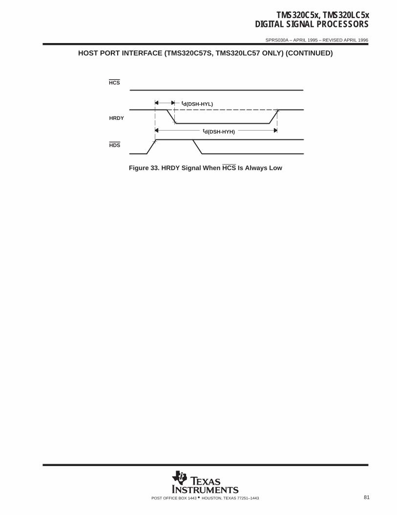
TMS320C5x, TMS320LC5xDIGITAL SIGNAL PROCESSORS
SPRS030A – APRIL 1995 – REVISED APRIL 1996
81POST OFFICE BOX 1443 • HOUSTON, TEXAS 77251–1443
HOST PORT INTERFACE (TMS320C57S, TMS320LC57 ONLY) (CONTINUED)
HRDY
HCS
td(DSH-HYL)
td(DSH-HYH)
HDS
Figure 33. HRDY Signal When HCS Is Always Low
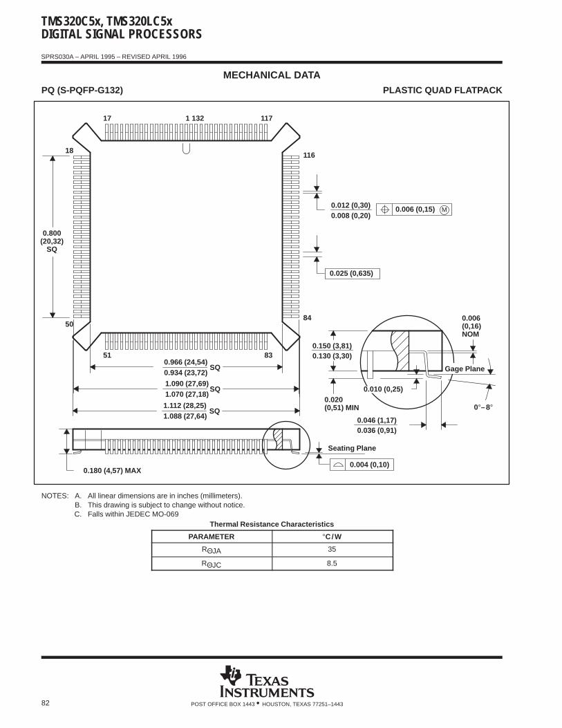
TMS320C5x, TMS320LC5xDIGITAL SIGNAL PROCESSORS
SPRS030A – APRIL 1995 – REVISED APRIL 1996
82 POST OFFICE BOX 1443 • HOUSTON, TEXAS 77251–1443
MECHANICAL DATAPQ (S-PQFP-G132) PLASTIC QUAD FLATPACK
116
0.012 (0,30)0.008 (0,20)
84
0.025 (0,635)
Seating Plane
0.966 (24,54)0.934 (23,72)
1.112 (28,25)1.088 (27,64)
0.800(20,32)
SQ
132117
8351
SQ
SQ
18
50
0.180 (4,57) MAX0.004 (0,10)
M0.006 (0,15)
0.020(0,51) MIN
0.130 (3,30)0.150 (3,81)
0.006(0,16)NOM
Gage Plane
0.036 (0,91)0.046 (1,17)
0°–8°
117
0.010 (0,25)1.090 (27,69)1.070 (27,18)
SQ
NOTES: A. All linear dimensions are in inches (millimeters).B. This drawing is subject to change without notice.C. Falls within JEDEC MO-069
Thermal Resistance Characteristics
PARAMETER °C/W
RΘJA 35
RΘJC 8.5
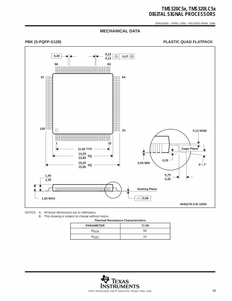
TMS320C5x, TMS320LC5xDIGITAL SIGNAL PROCESSORS
SPRS030A – APRIL 1995 – REVISED APRIL 1996
83POST OFFICE BOX 1443 • HOUSTON, TEXAS 77251–1443
MECHANICAL DATA
PBK (S-PQFP-G128) PLASTIC QUAD FLATPACK
4040279-3/B 10/94
64
33
Gage Plane
0,13 NOM
0,25
0,450,75
Seating Plane
0,05 MIN
0,23
65
32
96
1
11,60 TYP
0,13
97
128
SQ
SQ
13,80
16,2015,80
1,60 MAX
1,451,35
14,20
0°–7°
0,08
0,40 M0,07
NOTES: A. All linear dimensions are in millimeters.B. This drawing is subject to change without notice.
Thermal Resistance Characteristics
PARAMETER °C/W
RΘJA 58
RΘJC 10
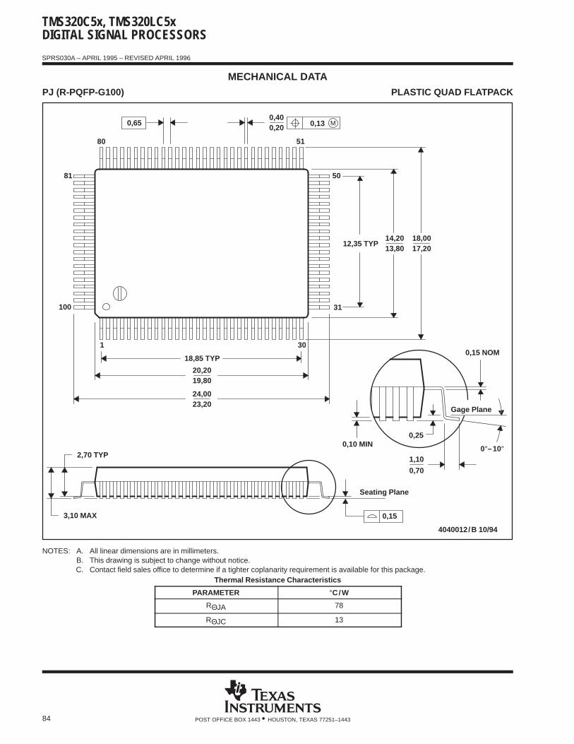
TMS320C5x, TMS320LC5xDIGITAL SIGNAL PROCESSORS
SPRS030A – APRIL 1995 – REVISED APRIL 1996
84 POST OFFICE BOX 1443 • HOUSTON, TEXAS 77251–1443
MECHANICAL DATAPJ (R-PQFP-G100) PLASTIC QUAD FLATPACK
4040012/B 10/94
0,15 NOM
18,0014,2017,2013,80
50
51
31
30
12,35 TYP
0,25
0,70
1,10
0,10 MIN
Gage Plane
80
1
18,85 TYP
81
100
20,2019,80
23,2024,00
3,10 MAX
2,70 TYP
0,200,40
Seating Plane
0,15
0,65 M0,13
0°–10°
NOTES: A. All linear dimensions are in millimeters.B. This drawing is subject to change without notice.C. Contact field sales office to determine if a tighter coplanarity requirement is available for this package.
Thermal Resistance Characteristics
PARAMETER °C/W
RΘJA 78
RΘJC 13
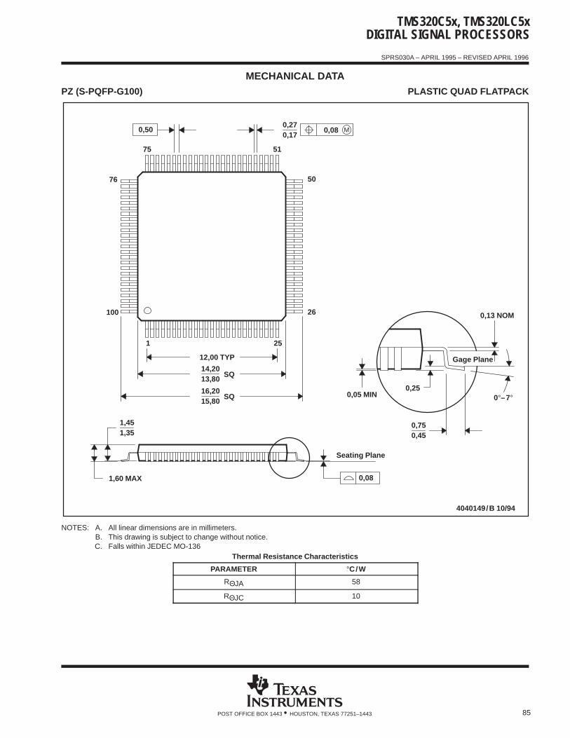
TMS320C5x, TMS320LC5xDIGITAL SIGNAL PROCESSORS
SPRS030A – APRIL 1995 – REVISED APRIL 1996
85POST OFFICE BOX 1443 • HOUSTON, TEXAS 77251–1443
MECHANICAL DATAPZ (S-PQFP-G100) PLASTIC QUAD FLATPACK
4040149/B 10/94
50
26 0,13 NOM
Gage Plane
0,25
0,450,75
0,05 MIN
0,27
51
25
75
1
12,00 TYP
0,17
76
100
SQ
SQ15,8016,20
13,80
1,351,45
1,60 MAX
14,20
0°–7°
Seating Plane
0,08
0,50 M0,08
NOTES: A. All linear dimensions are in millimeters.B. This drawing is subject to change without notice.C. Falls within JEDEC MO-136
Thermal Resistance Characteristics
PARAMETER °C/W
RΘJA 58
RΘJC 10
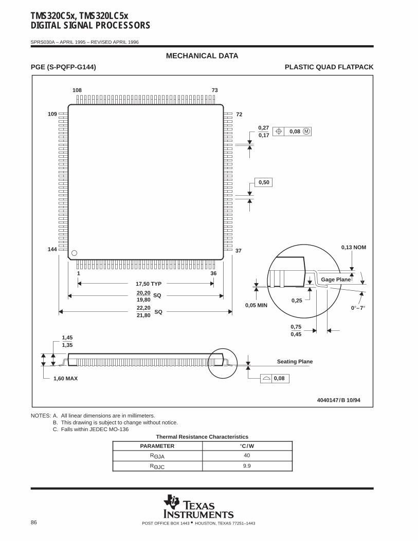
TMS320C5x, TMS320LC5xDIGITAL SIGNAL PROCESSORS
SPRS030A – APRIL 1995 – REVISED APRIL 1996
86 POST OFFICE BOX 1443 • HOUSTON, TEXAS 77251–1443
MECHANICAL DATAPGE (S-PQFP-G144) PLASTIC QUAD FLATPACK
4040147/B 10/94
0,27
72
0,17
37
73
0,13 NOM
0,25
0,750,45
0,05 MIN
36
Seating Plane
Gage Plane
108
109
144
SQ
SQ22,2021,80
1
19,80
17,50 TYP
20,20
1,351,45
1,60 MAX
M0,08
0°–7°
0,08
0,50
NOTES: A. All linear dimensions are in millimeters.B. This drawing is subject to change without notice.C. Falls within JEDEC MO-136
Thermal Resistance Characteristics
PARAMETER °C/W
RΘJA 40
RΘJC 9.9
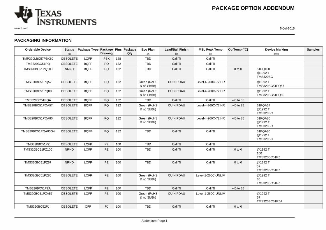
PACKAGE OPTION ADDENDUM
www.ti.com 5-Jul-2015
Addendum-Page 1
PACKAGING INFORMATION
Orderable Device Status(1)
Package Type PackageDrawing
Pins PackageQty
Eco Plan(2)
Lead/Ball Finish(6)
MSL Peak Temp(3)
Op Temp (°C) Device Marking(4/5)
Samples
TMP320LBC57PBK80 OBSOLETE LQFP PBK 128 TBD Call TI Call TI
TMS320BC51PQ OBSOLETE BQFP PQ 132 TBD Call TI Call TI
TMS320BC51PQ100 NRND BQFP PQ 132 TBD Call TI Call TI 0 to 0 51PQ100@1992 TITMS320BC
TMS320BC51PQ57 OBSOLETE BQFP PQ 132 Green (RoHS& no Sb/Br)
CU NIPDAU Level-4-260C-72 HR @1992 TITMS320BC51PQ57
TMS320BC51PQ80 OBSOLETE BQFP PQ 132 Green (RoHS& no Sb/Br)
CU NIPDAU Level-4-260C-72 HR @1992 TITMS320BC51PQ80
TMS320BC51PQA OBSOLETE BQFP PQ 132 TBD Call TI Call TI -40 to 85
TMS320BC51PQA57 OBSOLETE BQFP PQ 132 Green (RoHS& no Sb/Br)
CU NIPDAU Level-4-260C-72 HR -40 to 85 51PQA57@1992 TITMS320BC
TMS320BC51PQA80 OBSOLETE BQFP PQ 132 Green (RoHS& no Sb/Br)
CU NIPDAU Level-4-260C-72 HR -40 to 85 51PQA80@1992 TITMS320BC
TMS320BC51PQA80G4 OBSOLETE BQFP PQ 132 TBD Call TI Call TI 51PQA80@1992 TITMS320BC
TMS320BC51PZ OBSOLETE LQFP PZ 100 TBD Call TI Call TI
TMS320BC51PZ100 NRND LQFP PZ 100 TBD Call TI Call TI 0 to 0 @1992 TI100TMS320BC51PZ
TMS320BC51PZ57 NRND LQFP PZ 100 TBD Call TI Call TI 0 to 0 @1992 TI57TMS320BC51PZ
TMS320BC51PZ80 OBSOLETE LQFP PZ 100 Green (RoHS& no Sb/Br)
CU NIPDAU Level-1-260C-UNLIM @1992 TI80TMS320BC51PZ
TMS320BC51PZA OBSOLETE LQFP PZ 100 TBD Call TI Call TI -40 to 85
TMS320BC51PZA57 OBSOLETE LQFP PZ 100 Green (RoHS& no Sb/Br)
CU NIPDAU Level-1-260C-UNLIM @1992 TI57TMS320BC51PZA
TMS320BC52PJ OBSOLETE QFP PJ 100 TBD Call TI Call TI 0 to 0
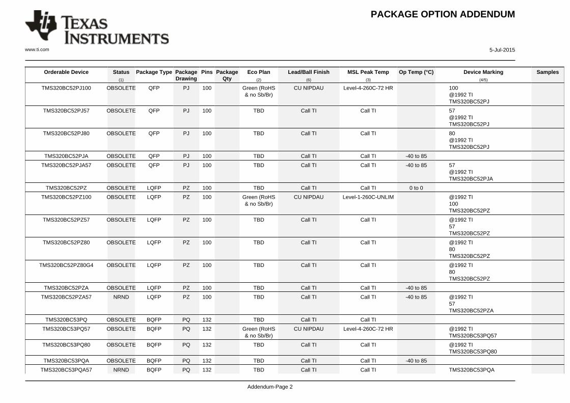
PACKAGE OPTION ADDENDUM
www.ti.com 5-Jul-2015
Addendum-Page 2
Orderable Device Status(1)
Package Type PackageDrawing
Pins PackageQty
Eco Plan(2)
Lead/Ball Finish(6)
MSL Peak Temp(3)
Op Temp (°C) Device Marking(4/5)
Samples
TMS320BC52PJ100 OBSOLETE QFP PJ 100 Green (RoHS& no Sb/Br)
CU NIPDAU Level-4-260C-72 HR 100@1992 TITMS320BC52PJ
TMS320BC52PJ57 OBSOLETE QFP PJ 100 TBD Call TI Call TI 57@1992 TITMS320BC52PJ
TMS320BC52PJ80 OBSOLETE QFP PJ 100 TBD Call TI Call TI 80@1992 TITMS320BC52PJ
TMS320BC52PJA OBSOLETE QFP PJ 100 TBD Call TI Call TI -40 to 85
TMS320BC52PJA57 OBSOLETE QFP PJ 100 TBD Call TI Call TI -40 to 85 57@1992 TITMS320BC52PJA
TMS320BC52PZ OBSOLETE LQFP PZ 100 TBD Call TI Call TI 0 to 0
TMS320BC52PZ100 OBSOLETE LQFP PZ 100 Green (RoHS& no Sb/Br)
CU NIPDAU Level-1-260C-UNLIM @1992 TI100TMS320BC52PZ
TMS320BC52PZ57 OBSOLETE LQFP PZ 100 TBD Call TI Call TI @1992 TI57TMS320BC52PZ
TMS320BC52PZ80 OBSOLETE LQFP PZ 100 TBD Call TI Call TI @1992 TI80TMS320BC52PZ
TMS320BC52PZ80G4 OBSOLETE LQFP PZ 100 TBD Call TI Call TI @1992 TI80TMS320BC52PZ
TMS320BC52PZA OBSOLETE LQFP PZ 100 TBD Call TI Call TI -40 to 85
TMS320BC52PZA57 NRND LQFP PZ 100 TBD Call TI Call TI -40 to 85 @1992 TI57TMS320BC52PZA
TMS320BC53PQ OBSOLETE BQFP PQ 132 TBD Call TI Call TI
TMS320BC53PQ57 OBSOLETE BQFP PQ 132 Green (RoHS& no Sb/Br)
CU NIPDAU Level-4-260C-72 HR @1992 TITMS320BC53PQ57
TMS320BC53PQ80 OBSOLETE BQFP PQ 132 TBD Call TI Call TI @1992 TITMS320BC53PQ80
TMS320BC53PQA OBSOLETE BQFP PQ 132 TBD Call TI Call TI -40 to 85
TMS320BC53PQA57 NRND BQFP PQ 132 TBD Call TI Call TI TMS320BC53PQA

PACKAGE OPTION ADDENDUM
www.ti.com 5-Jul-2015
Addendum-Page 3
Orderable Device Status(1)
Package Type PackageDrawing
Pins PackageQty
Eco Plan(2)
Lead/Ball Finish(6)
MSL Peak Temp(3)
Op Temp (°C) Device Marking(4/5)
Samples
@1992 TI57
TMS320BC53SPZ OBSOLETE LQFP PZ 100 TBD Call TI Call TI
TMS320BC53SPZ80 NRND LQFP PZ 100 TBD Call TI Call TI @1992 TI80TMS320BC53SPZ
TMS320BC57SPGE57 OBSOLETE LQFP PGE 144 TBD Call TI Call TI TMS320BC57SPGE@1995 TI57
TMS320BC57SPGE80 OBSOLETE LQFP PGE 144 TBD Call TI Call TI 80@1995 TITMS320BC57SPGE
TMS320C50PGE OBSOLETE LQFP PGE 144 TBD Call TI Call TI
TMS320C50PGE57 NRND LQFP PGE 144 TBD Call TI Call TI 57TMS320C50PGE
TMS320C50PGE80 NRND LQFP PGE 144 TBD Call TI Call TI TMS320C50PGE80
TMS320C50PGEA57 OBSOLETE LQFP PGE 144 Green (RoHS& no Sb/Br)
CU NIPDAU Level-1-260C-UNLIM 57TMS320C50PGEA
TMS320C50PQ OBSOLETE BQFP PQ 132 TBD Call TI Call TI
TMS320C50PQ57 OBSOLETE BQFP PQ 132 Green (RoHS& no Sb/Br)
CU NIPDAU Level-4-260C-72 HR TMS320C50PQ57@1992 TI
TMS320C50PQ80 OBSOLETE BQFP PQ 132 Green (RoHS& no Sb/Br)
CU NIPDAU Level-4-260C-72 HR TMS320C50PQ80@1992 TI
TMS320C50PQA OBSOLETE BQFP PQ 132 TBD Call TI Call TI -40 to 85 TMS320C50PQA@1992 TI
TMS320C50PQA57 OBSOLETE BQFP PQ 132 Green (RoHS& no Sb/Br)
CU NIPDAU Level-4-260C-72 HR -40 to 85 TMS320C50PQA57@1992 TI
TMS320C51PQ OBSOLETE BQFP PQ 132 TBD Call TI Call TI
TMS320C51PQ100 OBSOLETE BQFP PQ 132 TBD Call TI Call TI
TMS320C51PQ57 OBSOLETE BQFP PQ 132 TBD Call TI Call TI
TMS320C51PQ80 OBSOLETE BQFP PQ 132 TBD Call TI Call TI
TMS320C51PQA OBSOLETE BQFP PQ 132 TBD Call TI Call TI -40 to 85
TMS320C51PQA57 OBSOLETE BQFP PQ 132 TBD Call TI Call TI -40 to 85
TMS320C51PQA80 OBSOLETE BQFP PQ 132 TBD Call TI Call TI -40 to 85
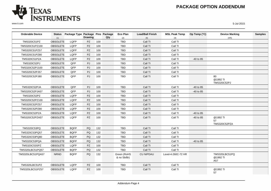
PACKAGE OPTION ADDENDUM
www.ti.com 5-Jul-2015
Addendum-Page 4
Orderable Device Status(1)
Package Type PackageDrawing
Pins PackageQty
Eco Plan(2)
Lead/Ball Finish(6)
MSL Peak Temp(3)
Op Temp (°C) Device Marking(4/5)
Samples
TMS320C51PZ OBSOLETE LQFP PZ 100 TBD Call TI Call TI
TMS320C51PZ100 OBSOLETE LQFP PZ 100 TBD Call TI Call TI
TMS320C51PZ57 OBSOLETE LQFP PZ 100 TBD Call TI Call TI
TMS320C51PZ80 OBSOLETE LQFP PZ 100 TBD Call TI Call TI
TMS320C51PZA OBSOLETE LQFP PZ 100 TBD Call TI Call TI -40 to 85
TMS320C52PJ OBSOLETE QFP PJ 100 TBD Call TI Call TI
TMS320C52PJ100 OBSOLETE QFP PJ 100 TBD Call TI Call TI
TMS320C52PJ57 OBSOLETE QFP PJ 100 TBD Call TI Call TI
TMS320C52PJ80 OBSOLETE QFP PJ 100 TBD Call TI Call TI 80@1992 TITMS320C52PJ
TMS320C52PJA OBSOLETE QFP PJ 100 TBD Call TI Call TI -40 to 85
TMS320C52PJA57 OBSOLETE QFP PJ 100 TBD Call TI Call TI -40 to 85
TMS320C52PZ OBSOLETE LQFP PZ 100 TBD Call TI Call TI
TMS320C52PZ100 OBSOLETE LQFP PZ 100 TBD Call TI Call TI
TMS320C52PZ57 OBSOLETE LQFP PZ 100 TBD Call TI Call TI
TMS320C52PZ80 OBSOLETE LQFP PZ 100 TBD Call TI Call TI
TMS320C52PZA OBSOLETE LQFP PZ 100 TBD Call TI Call TI -40 to 85
TMS320C52PZA57 OBSOLETE LQFP PZ 100 TBD Call TI Call TI -40 to 85 @1992 TI57TMS320C52PZA
TMS320C53PQ OBSOLETE BQFP PQ 132 TBD Call TI Call TI
TMS320C53PQ57 OBSOLETE BQFP PQ 132 TBD Call TI Call TI
TMS320C53PQ80 OBSOLETE BQFP PQ 132 TBD Call TI Call TI
TMS320C53PQA OBSOLETE BQFP PQ 132 TBD Call TI Call TI -40 to 85
TMS320C53SPZ OBSOLETE LQFP PZ 100 TBD Call TI Call TI
TMS320LBC51PQ57 OBSOLETE BQFP PQ 132 TBD Call TI Call TI
TMS320LBC51PQA57 NRND BQFP PQ 132 Green (RoHS& no Sb/Br)
CU NIPDAU Level-4-260C-72 HR TMS320LBC51PQ@1992 TIA57
TMS320LBC51PZ OBSOLETE LQFP PZ 100 TBD Call TI Call TI
TMS320LBC51PZ57 OBSOLETE LQFP PZ 100 TBD Call TI Call TI @1992 TI57
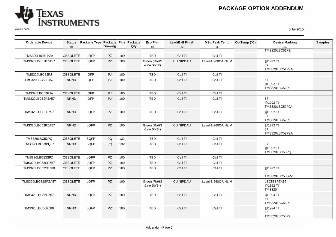
PACKAGE OPTION ADDENDUM
www.ti.com 5-Jul-2015
Addendum-Page 5
Orderable Device Status(1)
Package Type PackageDrawing
Pins PackageQty
Eco Plan(2)
Lead/Ball Finish(6)
MSL Peak Temp(3)
Op Temp (°C) Device Marking(4/5)
Samples
TMS320LBC51PZ
TMS320LBC51PZA OBSOLETE LQFP PZ 100 TBD Call TI Call TI
TMS320LBC51PZA57 OBSOLETE LQFP PZ 100 Green (RoHS& no Sb/Br)
CU NIPDAU Level-1-260C-UNLIM @1992 TI57TMS320LBC51PZA
TMS320LBC52PJ OBSOLETE QFP PJ 100 TBD Call TI Call TI
TMS320LBC52PJ57 NRND QFP PJ 100 TBD Call TI Call TI 57@1992 TITMS320LBC52PJ
TMS320LBC52PJA OBSOLETE QFP PJ 100 TBD Call TI Call TI
TMS320LBC52PJA57 NRND QFP PJ 100 TBD Call TI Call TI 57@1992 TITMS320LBC52PJA
TMS320LBC52PZ57 NRND LQFP PZ 100 TBD Call TI Call TI @1992 TI57TMS320LBC52PZ
TMS320LBC52PZA57 NRND LQFP PZ 100 Green (RoHS& no Sb/Br)
CU NIPDAU Level-1-260C-UNLIM @1992 TI57TMS320LBC52PZA
TMS320LBC53PQ OBSOLETE BQFP PQ 132 TBD Call TI Call TI
TMS320LBC53PQ57 NRND BQFP PQ 132 TBD Call TI Call TI 57@1992 TITMS320LBC53PQ
TMS320LBC53SPZ OBSOLETE LQFP PZ 100 TBD Call TI Call TI
TMS320LBC53SPZ57 OBSOLETE LQFP PZ 100 TBD Call TI Call TI
TMS320LBC53SPZ80 OBSOLETE LQFP PZ 100 TBD Call TI Call TI @1992 TI80TMS320LBC53SPZ
TMS320LBC53SPZA57 OBSOLETE LQFP PZ 100 Green (RoHS& no Sb/Br)
CU NIPDAU Level-1-260C-UNLIM LBC53SPZA57@1992 TITMS320
TMS320LBC56PZ57 NRND LQFP PZ 100 TBD Call TI Call TI @1994 TI57TMS320LBC56PZ
TMS320LBC56PZ80 NRND LQFP PZ 100 TBD Call TI Call TI @1994 TI80TMS320LBC56PZ
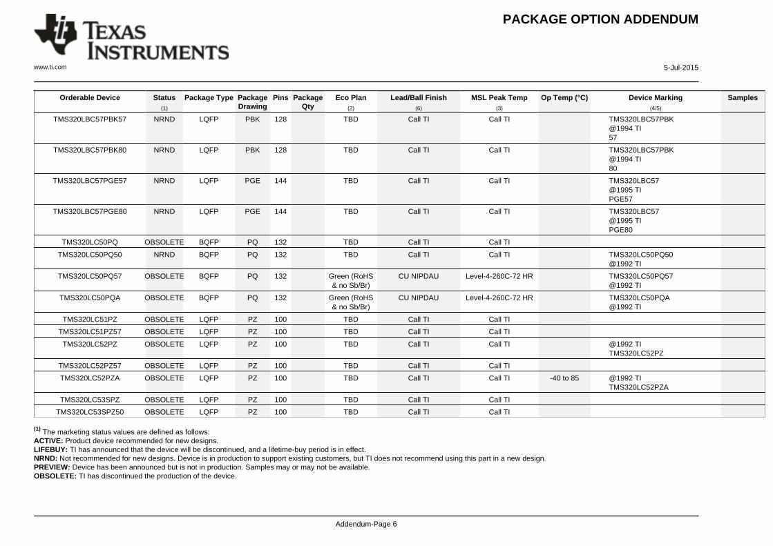
PACKAGE OPTION ADDENDUM
www.ti.com 5-Jul-2015
Addendum-Page 6
Orderable Device Status(1)
Package Type PackageDrawing
Pins PackageQty
Eco Plan(2)
Lead/Ball Finish(6)
MSL Peak Temp(3)
Op Temp (°C) Device Marking(4/5)
Samples
TMS320LBC57PBK57 NRND LQFP PBK 128 TBD Call TI Call TI TMS320LBC57PBK@1994 TI57
TMS320LBC57PBK80 NRND LQFP PBK 128 TBD Call TI Call TI TMS320LBC57PBK@1994 TI80
TMS320LBC57PGE57 NRND LQFP PGE 144 TBD Call TI Call TI TMS320LBC57@1995 TIPGE57
TMS320LBC57PGE80 NRND LQFP PGE 144 TBD Call TI Call TI TMS320LBC57@1995 TIPGE80
TMS320LC50PQ OBSOLETE BQFP PQ 132 TBD Call TI Call TI
TMS320LC50PQ50 NRND BQFP PQ 132 TBD Call TI Call TI TMS320LC50PQ50@1992 TI
TMS320LC50PQ57 OBSOLETE BQFP PQ 132 Green (RoHS& no Sb/Br)
CU NIPDAU Level-4-260C-72 HR TMS320LC50PQ57@1992 TI
TMS320LC50PQA OBSOLETE BQFP PQ 132 Green (RoHS& no Sb/Br)
CU NIPDAU Level-4-260C-72 HR TMS320LC50PQA@1992 TI
TMS320LC51PZ OBSOLETE LQFP PZ 100 TBD Call TI Call TI
TMS320LC51PZ57 OBSOLETE LQFP PZ 100 TBD Call TI Call TI
TMS320LC52PZ OBSOLETE LQFP PZ 100 TBD Call TI Call TI @1992 TITMS320LC52PZ
TMS320LC52PZ57 OBSOLETE LQFP PZ 100 TBD Call TI Call TI
TMS320LC52PZA OBSOLETE LQFP PZ 100 TBD Call TI Call TI -40 to 85 @1992 TITMS320LC52PZA
TMS320LC53SPZ OBSOLETE LQFP PZ 100 TBD Call TI Call TI
TMS320LC53SPZ50 OBSOLETE LQFP PZ 100 TBD Call TI Call TI (1) The marketing status values are defined as follows:ACTIVE: Product device recommended for new designs.LIFEBUY: TI has announced that the device will be discontinued, and a lifetime-buy period is in effect.NRND: Not recommended for new designs. Device is in production to support existing customers, but TI does not recommend using this part in a new design.PREVIEW: Device has been announced but is not in production. Samples may or may not be available.OBSOLETE: TI has discontinued the production of the device.
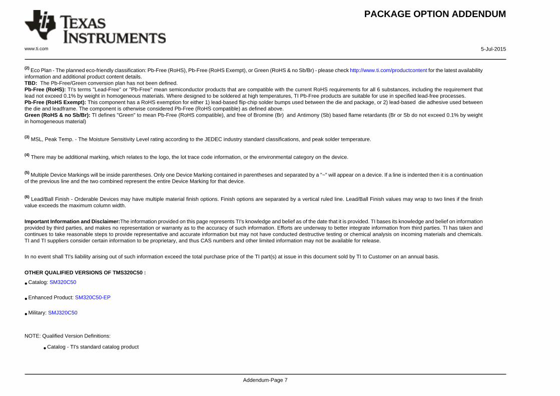
PACKAGE OPTION ADDENDUM
www.ti.com 5-Jul-2015
Addendum-Page 7
(2) Eco Plan - The planned eco-friendly classification: Pb-Free (RoHS), Pb-Free (RoHS Exempt), or Green (RoHS & no Sb/Br) - please check http://www.ti.com/productcontent for the latest availabilityinformation and additional product content details.TBD: The Pb-Free/Green conversion plan has not been defined.Pb-Free (RoHS): TI's terms "Lead-Free" or "Pb-Free" mean semiconductor products that are compatible with the current RoHS requirements for all 6 substances, including the requirement thatlead not exceed 0.1% by weight in homogeneous materials. Where designed to be soldered at high temperatures, TI Pb-Free products are suitable for use in specified lead-free processes.Pb-Free (RoHS Exempt): This component has a RoHS exemption for either 1) lead-based flip-chip solder bumps used between the die and package, or 2) lead-based die adhesive used betweenthe die and leadframe. The component is otherwise considered Pb-Free (RoHS compatible) as defined above.Green (RoHS & no Sb/Br): TI defines "Green" to mean Pb-Free (RoHS compatible), and free of Bromine (Br) and Antimony (Sb) based flame retardants (Br or Sb do not exceed 0.1% by weightin homogeneous material)
(3) MSL, Peak Temp. - The Moisture Sensitivity Level rating according to the JEDEC industry standard classifications, and peak solder temperature.
(4) There may be additional marking, which relates to the logo, the lot trace code information, or the environmental category on the device.
(5) Multiple Device Markings will be inside parentheses. Only one Device Marking contained in parentheses and separated by a "~" will appear on a device. If a line is indented then it is a continuationof the previous line and the two combined represent the entire Device Marking for that device.
(6) Lead/Ball Finish - Orderable Devices may have multiple material finish options. Finish options are separated by a vertical ruled line. Lead/Ball Finish values may wrap to two lines if the finishvalue exceeds the maximum column width.
Important Information and Disclaimer:The information provided on this page represents TI's knowledge and belief as of the date that it is provided. TI bases its knowledge and belief on informationprovided by third parties, and makes no representation or warranty as to the accuracy of such information. Efforts are underway to better integrate information from third parties. TI has taken andcontinues to take reasonable steps to provide representative and accurate information but may not have conducted destructive testing or chemical analysis on incoming materials and chemicals.TI and TI suppliers consider certain information to be proprietary, and thus CAS numbers and other limited information may not be available for release.
In no event shall TI's liability arising out of such information exceed the total purchase price of the TI part(s) at issue in this document sold by TI to Customer on an annual basis.
OTHER QUALIFIED VERSIONS OF TMS320C50 :
• Catalog: SM320C50
• Enhanced Product: SM320C50-EP
• Military: SMJ320C50
NOTE: Qualified Version Definitions:
• Catalog - TI's standard catalog product
PACKAGE OPTION ADDENDUM
www.ti.com 5-Jul-2015
Addendum-Page 8
• Enhanced Product - Supports Defense, Aerospace and Medical Applications
• Military - QML certified for Military and Defense Applications

IMPORTANT NOTICE
Texas Instruments Incorporated and its subsidiaries (TI) reserve the right to make corrections, enhancements, improvements and otherchanges to its semiconductor products and services per JESD46, latest issue, and to discontinue any product or service per JESD48, latestissue. Buyers should obtain the latest relevant information before placing orders and should verify that such information is current andcomplete. All semiconductor products (also referred to herein as “components”) are sold subject to TI’s terms and conditions of salesupplied at the time of order acknowledgment.TI warrants performance of its components to the specifications applicable at the time of sale, in accordance with the warranty in TI’s termsand conditions of sale of semiconductor products. Testing and other quality control techniques are used to the extent TI deems necessaryto support this warranty. Except where mandated by applicable law, testing of all parameters of each component is not necessarilyperformed.TI assumes no liability for applications assistance or the design of Buyers’ products. Buyers are responsible for their products andapplications using TI components. To minimize the risks associated with Buyers’ products and applications, Buyers should provideadequate design and operating safeguards.TI does not warrant or represent that any license, either express or implied, is granted under any patent right, copyright, mask work right, orother intellectual property right relating to any combination, machine, or process in which TI components or services are used. Informationpublished by TI regarding third-party products or services does not constitute a license to use such products or services or a warranty orendorsement thereof. Use of such information may require a license from a third party under the patents or other intellectual property of thethird party, or a license from TI under the patents or other intellectual property of TI.Reproduction of significant portions of TI information in TI data books or data sheets is permissible only if reproduction is without alterationand is accompanied by all associated warranties, conditions, limitations, and notices. TI is not responsible or liable for such altereddocumentation. Information of third parties may be subject to additional restrictions.Resale of TI components or services with statements different from or beyond the parameters stated by TI for that component or servicevoids all express and any implied warranties for the associated TI component or service and is an unfair and deceptive business practice.TI is not responsible or liable for any such statements.Buyer acknowledges and agrees that it is solely responsible for compliance with all legal, regulatory and safety-related requirementsconcerning its products, and any use of TI components in its applications, notwithstanding any applications-related information or supportthat may be provided by TI. Buyer represents and agrees that it has all the necessary expertise to create and implement safeguards whichanticipate dangerous consequences of failures, monitor failures and their consequences, lessen the likelihood of failures that might causeharm and take appropriate remedial actions. Buyer will fully indemnify TI and its representatives against any damages arising out of the useof any TI components in safety-critical applications.In some cases, TI components may be promoted specifically to facilitate safety-related applications. With such components, TI’s goal is tohelp enable customers to design and create their own end-product solutions that meet applicable functional safety standards andrequirements. Nonetheless, such components are subject to these terms.No TI components are authorized for use in FDA Class III (or similar life-critical medical equipment) unless authorized officers of the partieshave executed a special agreement specifically governing such use.Only those TI components which TI has specifically designated as military grade or “enhanced plastic” are designed and intended for use inmilitary/aerospace applications or environments. Buyer acknowledges and agrees that any military or aerospace use of TI componentswhich have not been so designated is solely at the Buyer's risk, and that Buyer is solely responsible for compliance with all legal andregulatory requirements in connection with such use.TI has specifically designated certain components as meeting ISO/TS16949 requirements, mainly for automotive use. In any case of use ofnon-designated products, TI will not be responsible for any failure to meet ISO/TS16949.
Products ApplicationsAudio www.ti.com/audio Automotive and Transportation www.ti.com/automotiveAmplifiers amplifier.ti.com Communications and Telecom www.ti.com/communicationsData Converters dataconverter.ti.com Computers and Peripherals www.ti.com/computersDLP® Products www.dlp.com Consumer Electronics www.ti.com/consumer-appsDSP dsp.ti.com Energy and Lighting www.ti.com/energyClocks and Timers www.ti.com/clocks Industrial www.ti.com/industrialInterface interface.ti.com Medical www.ti.com/medicalLogic logic.ti.com Security www.ti.com/securityPower Mgmt power.ti.com Space, Avionics and Defense www.ti.com/space-avionics-defenseMicrocontrollers microcontroller.ti.com Video and Imaging www.ti.com/videoRFID www.ti-rfid.comOMAP Applications Processors www.ti.com/omap TI E2E Community e2e.ti.comWireless Connectivity www.ti.com/wirelessconnectivity
Mailing Address: Texas Instruments, Post Office Box 655303, Dallas, Texas 75265Copyright © 2015, Texas Instruments Incorporated


![Algorithms in Signal Processors Audio Applications · PDF fileAlgorithms in Signal Processors Audio Applications 2005 ... autocorrelation[lag] = XN n=0 signal[n] ... maximum lag of](https://img.dokumen.tips/doc/110x75/5a9d9e777f8b9a28388c5ccd/algorithms-in-signal-processors-audio-applications-in-signal-processors-audio-applications.jpg)