Embed Size (px)
Citation preview
Digital Design:An Embedded Systems Approach Using Verilog
Chapter 5
Memories
Portions of this work are from the book, Digital Design: An Embedded Systems Approach Using Verilog, by Peter J. Ashenden, published by Morgan Kaufmann Publishers, Copyright 2007 Elsevier Inc. All rights reserved.
Verilog
Digital Design — Chapter 5 — Memories 2
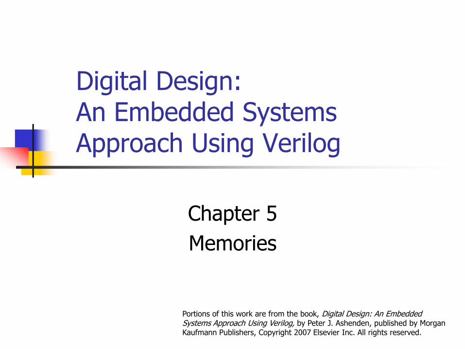
General Concepts
A memory is an array of storage locations
Each with a unique address
Like a collection of registers, but with optimized implementation
Address is unsigned-binary encoded
n address bits ⇒ 2n locations
All locations the same size
2n × m bit memory
0
1
2
3
4
5
6
2n–2
2n–1
m bits
Verilog
Digital Design — Chapter 5 — Memories 3
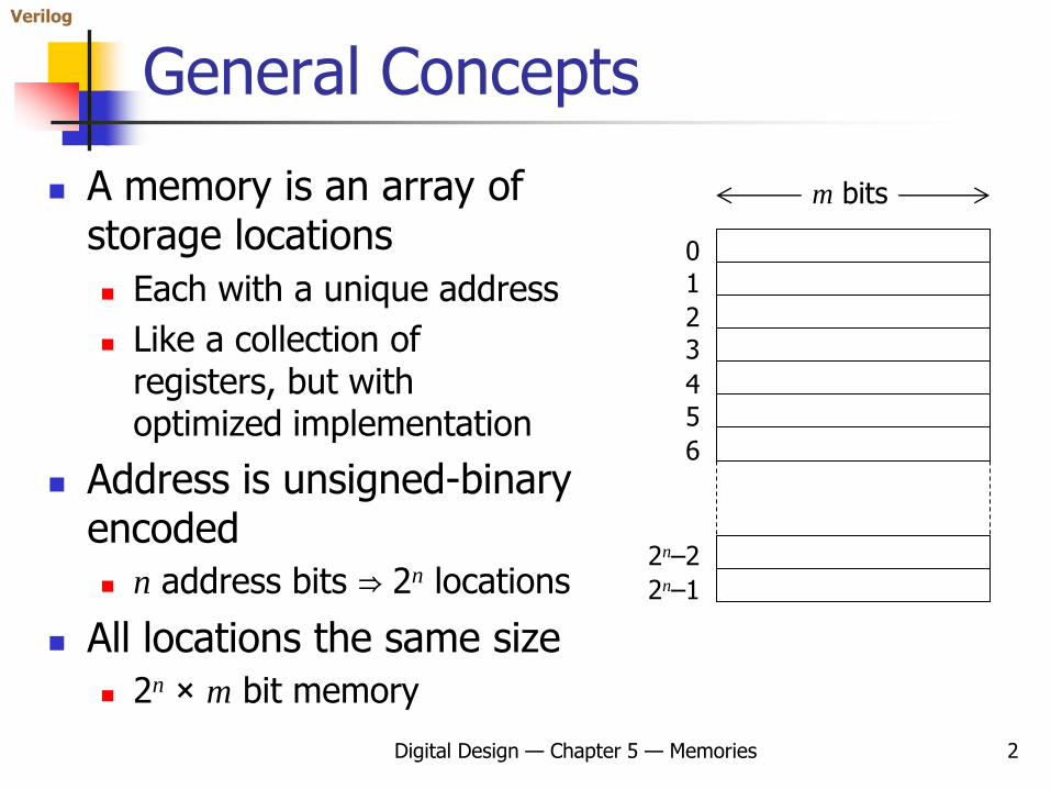
Memory Sizes
Use power-of-2 multipliers
Kilo (K): 210 = 1,024 ≈ 103
Mega (M): 220 = 1,048,576 ≈ 106
Giga (G): 230 = 1,073,741,824 ≈ 109
Example
32K × 32-bit memory
Capacity = 1,024K = 1Mbit
Requires 15 address bits
Size is determined by application requirements

Verilog
Digital Design — Chapter 5 — Memories 4
Basic Memory Operations
a inputs: unsigned address d_in and d_out
Type depends on application
Write operation en = 1, wr = 1 d_in value stored in location given
by address inputs
Read operation en = 1, wr = 0 d_out driven with value of location
given by address inputs
Idle: en = 0
n
m m
Verilog
Digital Design — Chapter 5 — Memories 5
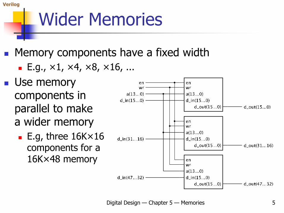
Wider Memories
Memory components have a fixed width
E.g., ×1, ×4, ×8, ×16, ...
Use memorycomponents inparallel to makea wider memory
E.g, three 16K×16components for a16K×48 memory
Verilog
Digital Design — Chapter 5 — Memories 6
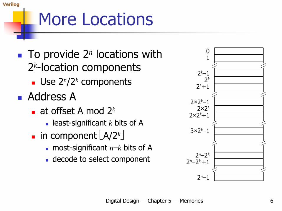
More Locations
To provide 2n locations with 2k-location components
Use 2n/2k components
Address A
at offset A mod 2k
least-significant k bits of A
in component A/2k
most-significant n–k bits of A
decode to select component
01
2k–12k
2k+1
2×2k–12×2k
2×2k+1
3×2k–1
2n–2k
2n–2k +1
2n–1
Verilog
Digital Design — Chapter 5 — Memories 7
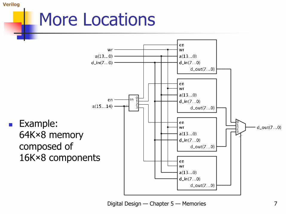
More Locations
Example:64K×8 memory
composed of16K×8 components
Verilog
Digital Design — Chapter 5 — Memories 8
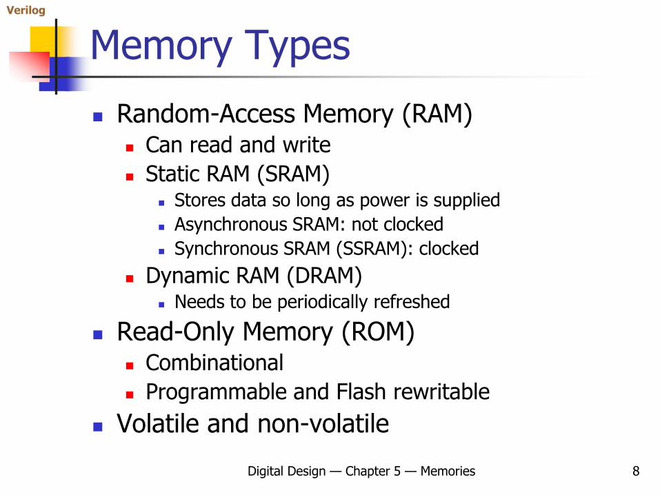
Memory Types
Random-Access Memory (RAM) Can read and write
Static RAM (SRAM) Stores data so long as power is supplied
Asynchronous SRAM: not clocked
Synchronous SRAM (SSRAM): clocked
Dynamic RAM (DRAM) Needs to be periodically refreshed
Read-Only Memory (ROM) Combinational
Programmable and Flash rewritable
Volatile and non-volatile
Verilog
Digital Design — Chapter 5 — Memories 9
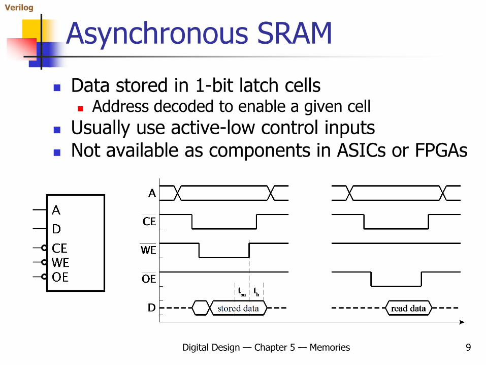
Asynchronous SRAM
Data stored in 1-bit latch cells Address decoded to enable a given cell
Usually use active-low control inputs Not available as components in ASICs or FPGAs
Verilog
Digital Design — Chapter 5 — Memories 10
Asynch SRAM Timing
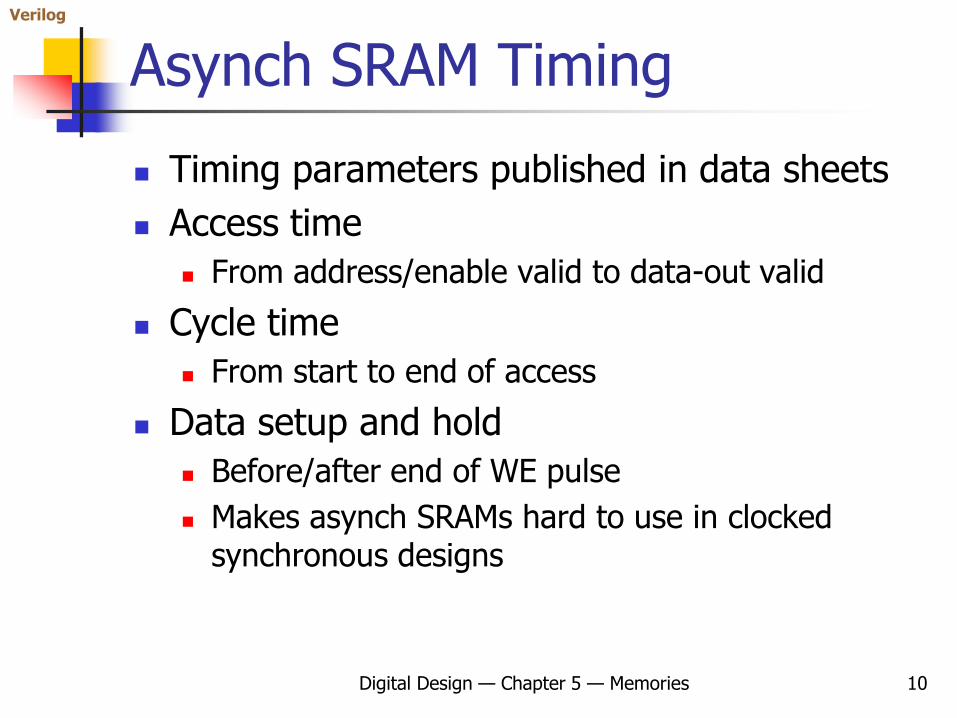
Timing parameters published in data sheets
Access time
From address/enable valid to data-out valid
Cycle time
From start to end of access
Data setup and hold
Before/after end of WE pulse
Makes asynch SRAMs hard to use in clocked synchronous designs
Verilog
Digital Design — Chapter 5 — Memories 11
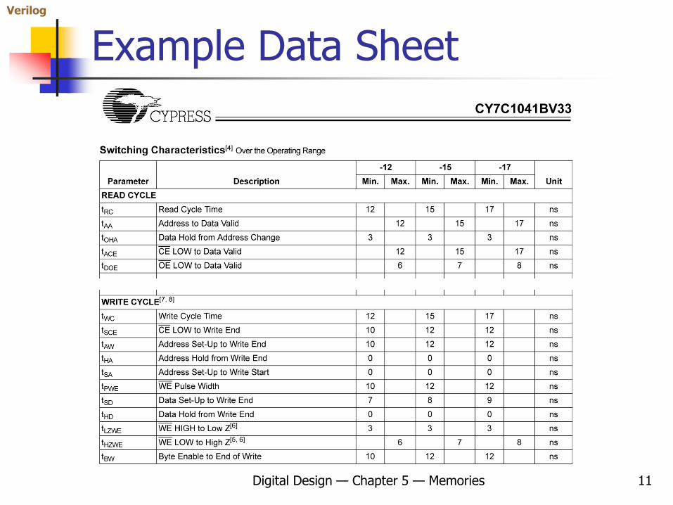
Example Data Sheet
Verilog
Digital Design — Chapter 5 — Memories 12
Synchronous SRAM (SSRAM)
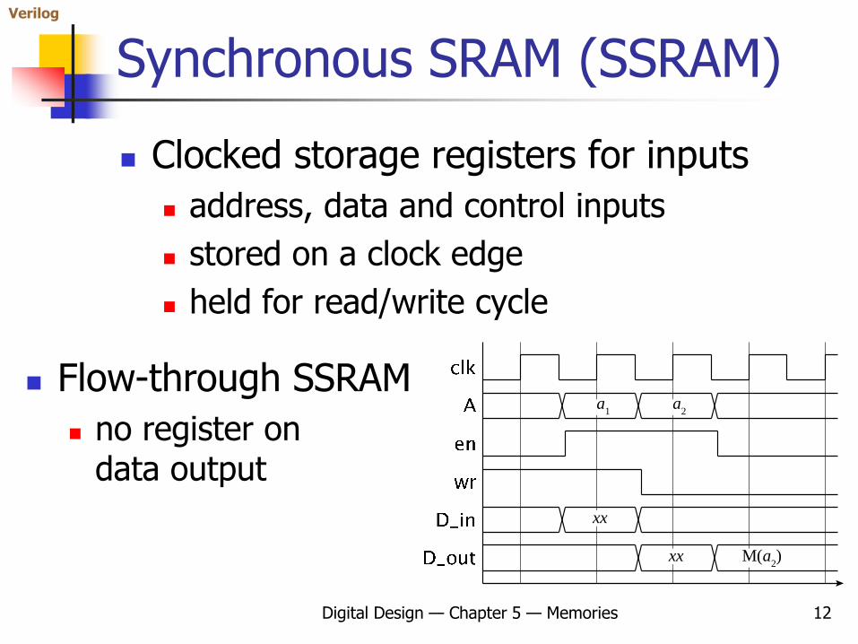
Clocked storage registers for inputs
address, data and control inputs
stored on a clock edge
held for read/write cycle
Flow-through SSRAM
no register ondata output
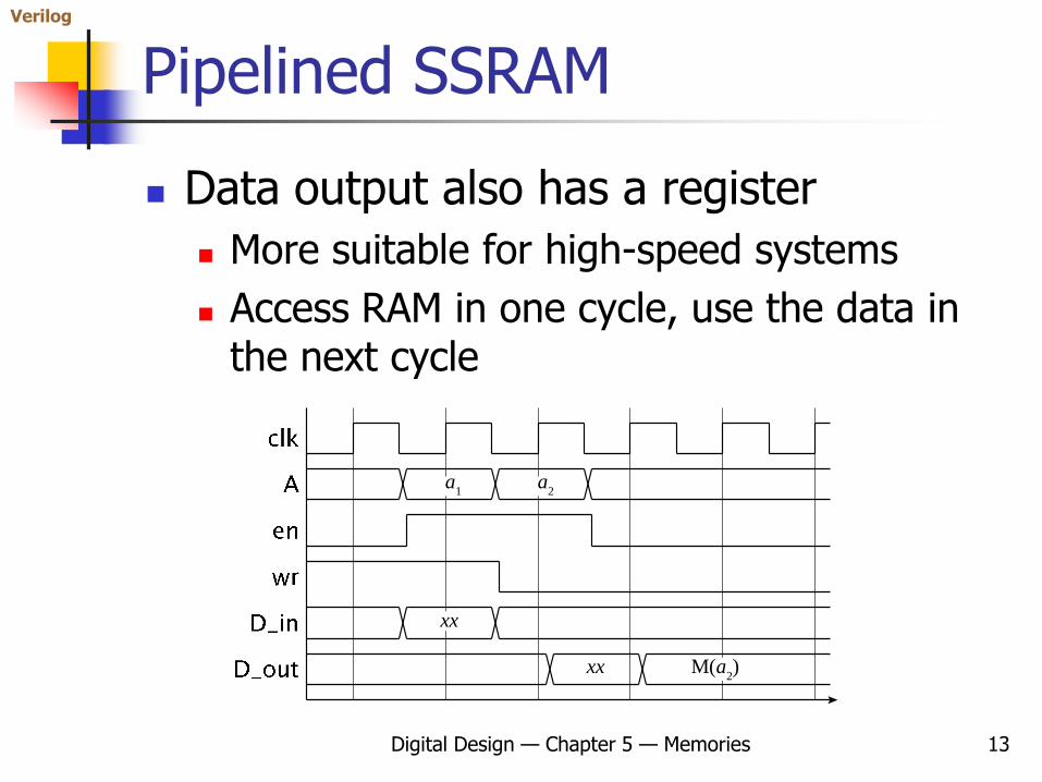
a1
xx
xx M(a2)
a2
Verilog
Digital Design — Chapter 5 — Memories 13
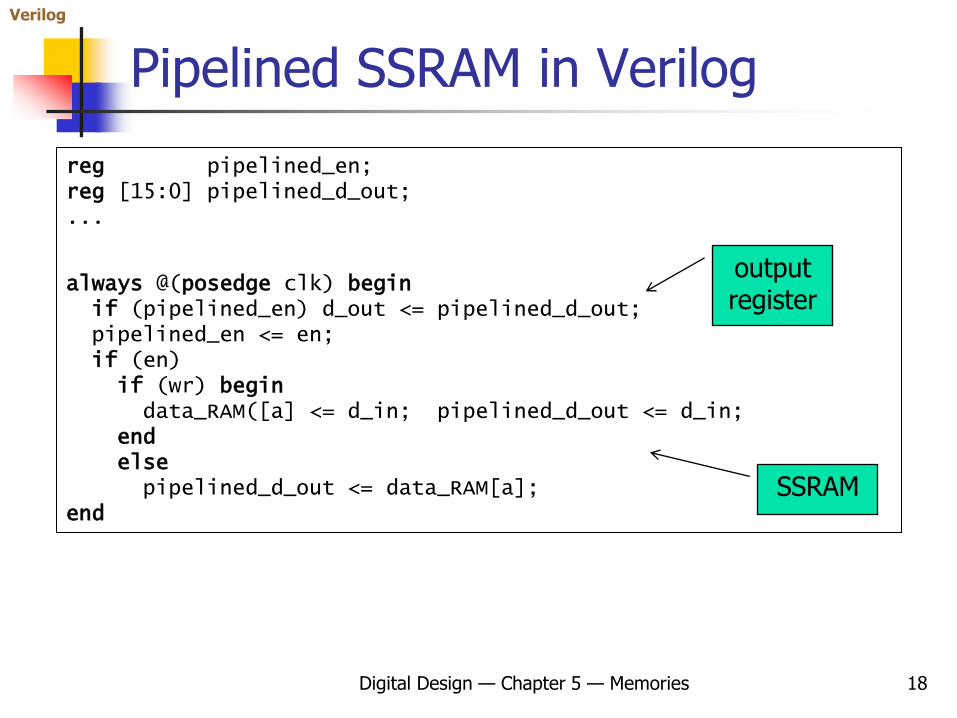
Pipelined SSRAM
Data output also has a register
More suitable for high-speed systems
Access RAM in one cycle, use the data in the next cycle
a1
xx
xx M(a2)
a2
Verilog
Digital Design — Chapter 5 — Memories 14
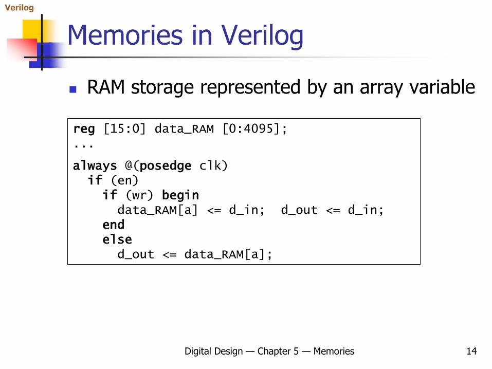
Memories in Verilog
RAM storage represented by an array variable
reg [15:0] data_RAM [0:4095];...
always @(posedge clk)if (en)
if (wr) begindata_RAM[a] <= d_in; d_out <= d_in;
endelse
d_out <= data_RAM[a];
Verilog
Digital Design — Chapter 5 — Memories 15
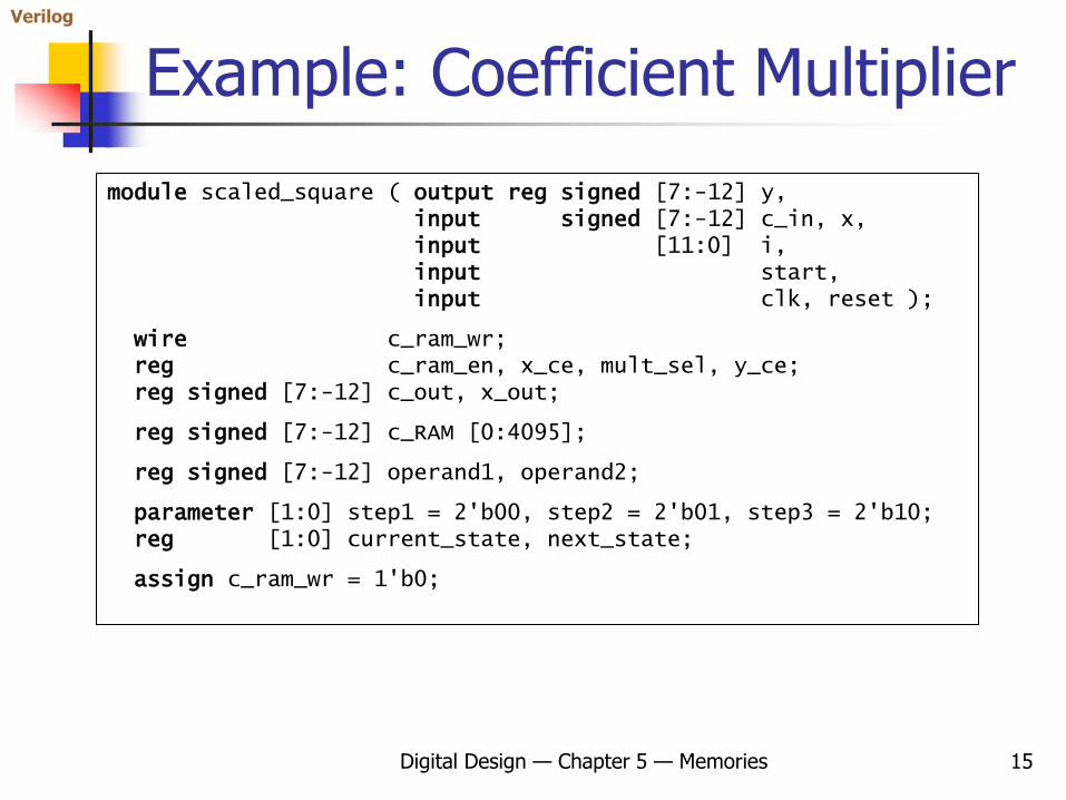
Example: Coefficient Multiplier
module scaled_square ( output reg signed [7:-12] y,input signed [7:-12] c_in, x,input [11:0] i,input start,input clk, reset );
wire c_ram_wr;reg c_ram_en, x_ce, mult_sel, y_ce;reg signed [7:-12] c_out, x_out;
reg signed [7:-12] c_RAM [0:4095];
reg signed [7:-12] operand1, operand2;
parameter [1:0] step1 = 2'b00, step2 = 2'b01, step3 = 2'b10;reg [1:0] current_state, next_state;
assign c_ram_wr = 1'b0;
Verilog
Digital Design — Chapter 5 — Memories 16
Example: Coefficient Multiplier
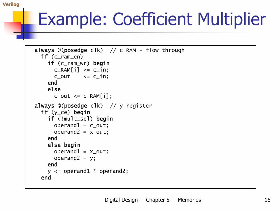
always @(posedge clk) // c RAM - flow throughif (c_ram_en)if (c_ram_wr) beginc_RAM[i] <= c_in;c_out <= c_in;
endelsec_out <= c_RAM[i];
always @(posedge clk) // y registerif (y_ce) beginif (!mult_sel) beginoperand1 = c_out;operand2 = x_out;
endelse beginoperand1 = x_out;operand2 = y;
endy <= operand1 * operand2;
end
Verilog
Digital Design — Chapter 5 — Memories 17
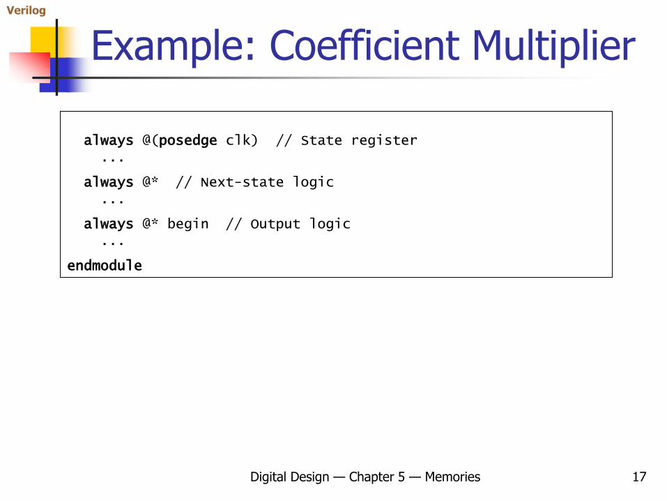
Example: Coefficient Multiplier
always @(posedge clk) // State register...
always @* // Next-state logic...
always @* begin // Output logic...
endmodule
Verilog
Digital Design — Chapter 5 — Memories 18
Pipelined SSRAM in Verilog
reg pipelined_en;reg [15:0] pipelined_d_out;...
always @(posedge clk) beginif (pipelined_en) d_out <= pipelined_d_out;pipelined_en <= en;if (en)if (wr) begindata_RAM([a] <= d_in; pipelined_d_out <= d_in;
endelsepipelined_d_out <= data_RAM[a];
endSSRAM
output register
Verilog
Digital Design — Chapter 5 — Memories 19
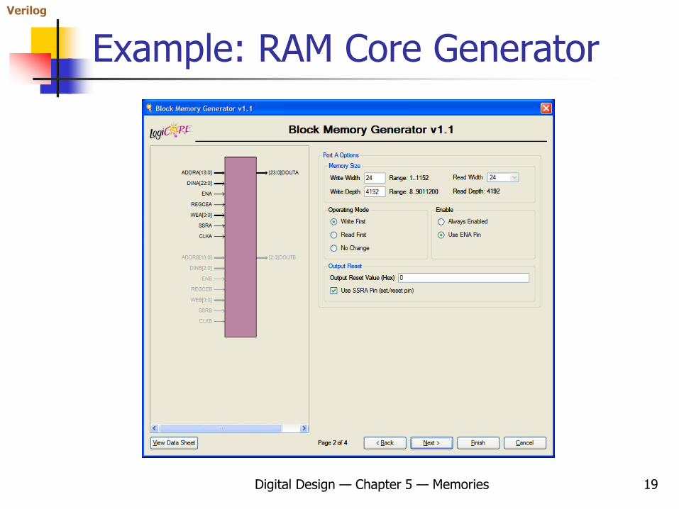
Example: RAM Core Generator


![[Sample Course Title Slide Insert Presentation Title]tinoosh/cmpe650/slides/power-estimat… · Design phase: Power can be calculated more accurately based on detailed information](https://img.dokumen.tips/doc/110x75/5fb331e5d074ea3cd07ecd66/sample-course-title-slide-insert-presentation-title-tinooshcmpe650slidespower-estimat.jpg)